KR20130109330A - Solar cell and method of fabricating the same - Google Patents
Solar cell and method of fabricating the sameDownload PDFInfo
- Publication number
- KR20130109330A KR20130109330AKR1020120030969AKR20120030969AKR20130109330AKR 20130109330 AKR20130109330 AKR 20130109330AKR 1020120030969 AKR1020120030969 AKR 1020120030969AKR 20120030969 AKR20120030969 AKR 20120030969AKR 20130109330 AKR20130109330 AKR 20130109330A
- Authority
- KR
- South Korea
- Prior art keywords
- layer
- electrode layer
- light absorbing
- solar cell
- buffer layer
- Prior art date
- Legal status (The legal status is an assumption and is not a legal conclusion. Google has not performed a legal analysis and makes no representation as to the accuracy of the status listed.)
- Ceased
Links
Images


Classifications
- H—ELECTRICITY
- H10—SEMICONDUCTOR DEVICES; ELECTRIC SOLID-STATE DEVICES NOT OTHERWISE PROVIDED FOR
- H10F—INORGANIC SEMICONDUCTOR DEVICES SENSITIVE TO INFRARED RADIATION, LIGHT, ELECTROMAGNETIC RADIATION OF SHORTER WAVELENGTH OR CORPUSCULAR RADIATION
- H10F19/00—Integrated devices, or assemblies of multiple devices, comprising at least one photovoltaic cell covered by group H10F10/00, e.g. photovoltaic modules
- H10F19/30—Integrated devices, or assemblies of multiple devices, comprising at least one photovoltaic cell covered by group H10F10/00, e.g. photovoltaic modules comprising thin-film photovoltaic cells
- H10F19/31—Integrated devices, or assemblies of multiple devices, comprising at least one photovoltaic cell covered by group H10F10/00, e.g. photovoltaic modules comprising thin-film photovoltaic cells having multiple laterally adjacent thin-film photovoltaic cells deposited on the same substrate
- H10F19/35—Structures for the connecting of adjacent photovoltaic cells, e.g. interconnections or insulating spacers
- H—ELECTRICITY
- H10—SEMICONDUCTOR DEVICES; ELECTRIC SOLID-STATE DEVICES NOT OTHERWISE PROVIDED FOR
- H10F—INORGANIC SEMICONDUCTOR DEVICES SENSITIVE TO INFRARED RADIATION, LIGHT, ELECTROMAGNETIC RADIATION OF SHORTER WAVELENGTH OR CORPUSCULAR RADIATION
- H10F19/00—Integrated devices, or assemblies of multiple devices, comprising at least one photovoltaic cell covered by group H10F10/00, e.g. photovoltaic modules
- H10F19/30—Integrated devices, or assemblies of multiple devices, comprising at least one photovoltaic cell covered by group H10F10/00, e.g. photovoltaic modules comprising thin-film photovoltaic cells
- H10F19/31—Integrated devices, or assemblies of multiple devices, comprising at least one photovoltaic cell covered by group H10F10/00, e.g. photovoltaic modules comprising thin-film photovoltaic cells having multiple laterally adjacent thin-film photovoltaic cells deposited on the same substrate
- H10F19/33—Patterning processes to connect the photovoltaic cells, e.g. laser cutting of conductive or active layers
- H—ELECTRICITY
- H10—SEMICONDUCTOR DEVICES; ELECTRIC SOLID-STATE DEVICES NOT OTHERWISE PROVIDED FOR
- H10F—INORGANIC SEMICONDUCTOR DEVICES SENSITIVE TO INFRARED RADIATION, LIGHT, ELECTROMAGNETIC RADIATION OF SHORTER WAVELENGTH OR CORPUSCULAR RADIATION
- H10F71/00—Manufacture or treatment of devices covered by this subclass
- Y—GENERAL TAGGING OF NEW TECHNOLOGICAL DEVELOPMENTS; GENERAL TAGGING OF CROSS-SECTIONAL TECHNOLOGIES SPANNING OVER SEVERAL SECTIONS OF THE IPC; TECHNICAL SUBJECTS COVERED BY FORMER USPC CROSS-REFERENCE ART COLLECTIONS [XRACs] AND DIGESTS
- Y02—TECHNOLOGIES OR APPLICATIONS FOR MITIGATION OR ADAPTATION AGAINST CLIMATE CHANGE
- Y02E—REDUCTION OF GREENHOUSE GAS [GHG] EMISSIONS, RELATED TO ENERGY GENERATION, TRANSMISSION OR DISTRIBUTION
- Y02E10/00—Energy generation through renewable energy sources
- Y02E10/50—Photovoltaic [PV] energy
Landscapes
- Photovoltaic Devices (AREA)
- Life Sciences & Earth Sciences (AREA)
- Engineering & Computer Science (AREA)
- Sustainable Development (AREA)
- Sustainable Energy (AREA)
Abstract
Translated fromKoreanDescription
Translated fromKorean실시예는 태양전지 및 이의 제조 방법에 관한 것이다.An embodiment relates to a solar cell and a manufacturing method thereof.
태양광을 전기 에너지로 변환시키기 위한 태양광 발전 장치는 태양전지 패널, 다이오드 및 프레임 등을 포함한다.Photovoltaic devices for converting sunlight into electrical energy include solar panels, diodes and frames.
상기 태양전지 패널은 플레이트 형상을 가진다. 예를 들어, 상기 태양전지 패널은 사각 플레이트 형상을 가진다. 상기 태양전지 패널은 상기 프레임 내측에 배치된다. 상기 태양전지 패널의 4개의 측면이 상기 프레임 내측에 배치된다.The solar cell panel has a plate shape. For example, the solar cell panel has a rectangular plate shape. The solar cell panel is disposed inside the frame. Four side surfaces of the solar cell panel are disposed inside the frame.
상기 태양전지 패널은 태양광을 입사받아, 전기 에너지로 변화시킨다. 상기 태양전지 패널은 다수 개의 태양전지 셀들을 포함한다. 또한, 상기 태양전지 패널은 상기 태양전지 셀들을 보호하기 위한 기판, 필름 또는 보호유리 등을 더 포함할 수 있다.The solar cell panel receives sunlight and changes it into electrical energy. The solar cell panel includes a plurality of solar cells. The solar cell panel may further include a substrate, a film or a protective glass for protecting the solar cells.
또한, 상기 태양전지 패널은 상기 태양전지 셀들에 접속되는 버스 바를 포함한다. 상기 버스 바는 최외곽의 태양전지 셀들의 상면으로부터 각각 연장되어 배선에 연결된다.In addition, the solar cell panel includes a bus bar connected to the solar cell. The bus bars extend from the upper surface of the outermost solar cells and are connected to the wirings.
상기 다이오드는 상기 태양전지 패널과 병렬로 연결된다. 상기 다이오드에는 선택적으로 전류가 흐른다. 즉, 상기 태양전지 패널의 성능이 저하되는 경우, 상기 다이오드를 통하여 전류가 흐른다. 이에 따라서, 실시예에 따른 태양광 발전 장치 자체의 단락이 방지된다. 또한, 태양광 발전 장치는 상기 다이오드 및 상기 태양전지 패널에 연결되는 배선을 더 포함할 수 있다. 상기 배선은 서로 인접하는 태양전지 패널을 연결한다.The diode is connected in parallel with the solar cell panel. An electric current flows selectively in the diode. That is, when the performance of the solar cell panel deteriorates, current flows through the diode. Accordingly, the short circuit of the photovoltaic device itself according to the embodiment is prevented. In addition, the photovoltaic device may further include a wire connected to the diode and the solar cell panel. The wiring connects solar cell panels adjacent to each other.
상기 프레임은 상기 태양전지 패널을 수용한다. 상기 프레임은 금속으로 이루어진다. 상기 프레임은 상기 태양전지 패널의 측면에 배치된다. 상기 프레임은 상기 태양전지 패널의 측면을 수용한다. 또한, 상기 프레임은 다수 개의 서브 프레임들로 이루어질 수 있다. 이때, 상기 서브 프레임들은 서로 연결될 수 있다.The frame houses the solar cell panel. The frame is made of metal. The frame is disposed on a side surface of the solar cell panel. The frame houses a side surface of the solar cell panel. Also, the frame may be composed of a plurality of subframes. At this time, the subframes may be connected to each other.
이와 같은 태양광 발전 장치는 야외에 장착되어, 태양광을 전기 에너지로 변환시킨다. 이때, 태양광 발전 장치는 외부의 물리적인 충격, 전기적인 충격 및 화학적인 충격에 노출될 수 있다.Such a photovoltaic device is mounted outdoors to convert sunlight into electrical energy. In this case, the photovoltaic device may be exposed to external physical shocks, electrical shocks, and chemical shocks.
이와 같은 태양광 발전 장치와 관련된 기술은 한국 공개 특허 공보 10-2009-0059529 등에 기재되어 있다.The technology related to such a photovoltaic device is described in Korean Unexamined Patent Publication No. 10-2009-0059529.
실시예는 단락을 방지하고, 향상된 성능을 가지는 태양 전지 및 이의 제조 방법을 제공하고자 한다.The embodiment seeks to provide a solar cell and a method of manufacturing the same, which prevent short circuiting and have improved performance.
실시예에 따른 태양 전지는, 지지 기판; 상기 지지 기판 상에 배치되는 후면 전극층; 상기 후면 전극층 상에 배치되는 광 흡수층; 상기 광 흡수층 상에 배치되는 버퍼층; 상기 버퍼층 상에 배치되는 전면전극층; 상기 광 흡수층을 관통하며, 상기 후면 전극층과 상기 전면 전극층을 전기적으로 연결하는 접속 배선; 및 상기 접속 배선의 측면 중 어느 하나의 측면에 형성되는 측면 절연부를 포함하고, 상기 측면 절연부는 상기 후면 전극층, 상기 광 흡수층 및 상기 버퍼층의 일부와 직접 접촉한다.According to an embodiment, a solar cell includes a support substrate; A rear electrode layer disposed on the support substrate; A light absorbing layer disposed on the rear electrode layer; A buffer layer disposed on the light absorbing layer; A front electrode layer disposed on the buffer layer; A connection wiring penetrating the light absorption layer and electrically connecting the rear electrode layer and the front electrode layer; And a side insulation portion formed on one side of the side surface of the connection wiring, wherein the side insulation portion is in direct contact with a portion of the back electrode layer, the light absorbing layer, and the buffer layer.
실시예에 따른 태양 전지 제조 방법은, 지지 기판 상에 후면 전극층을 형성하는 단계; 상기 후면 전극층 상에 광 흡수층을 형성하는 단계; 상기 광 흡수층 상에 버퍼층을 형성하는 단계; 상기 버퍼층, 상기 광 흡수층 및 상기 후면 전극층을 관통하는 관통홈을 형성하는 단계; 상기 관통홈의 측면에 측면 절연부를 형성하는 단계; 및 상기 버퍼층 상에 접속 배선 및 전면 전극층을 형성하는 단계를 포함한다.A solar cell manufacturing method according to an embodiment includes forming a back electrode layer on a support substrate; Forming a light absorbing layer on the back electrode layer; Forming a buffer layer on the light absorbing layer; Forming a through hole penetrating the buffer layer, the light absorbing layer, and the back electrode layer; Forming a side insulation on a side of the through groove; And forming a connection line and a front electrode layer on the buffer layer.
실시예에 따른 태양 전지 및 이의 제조 방법은 제 1 관통홈의 측면, 또는, 상기 접속 배선(600)의 측면에 형성되는 측면 절연부를 포함하는 태양 전지를 제공한다.The solar cell and the method of manufacturing the same according to the embodiment provide a solar cell including a side insulation portion formed on a side surface of the first through hole or on the side of the
또한, 실시예에 따른 태양 전지 및 이의 제조 방법은 상기 제 1 관통홈에 의해, 상기 후면 전극층의 분리 및 상기 전면 전극층과 상기 후면 전극층을 연결할 수 있다.In addition, the solar cell and the method of manufacturing the same according to the embodiment may be separated from the rear electrode layer and the front electrode layer and the rear electrode layer by the first through groove.
즉, 종래 상기 후면 전극층의 분리와 상기 전면 전극층과 상기 후면 전극층을 연결을 위한 관통홈들을 각각 형성하였던 것과 비교하여, 태양 전지로서 작동할 수 없는 영역 즉, 데드존(dead zone) 영역을 감소할 수 있다.That is, as compared with the conventional separation of the rear electrode layer and through holes for connecting the front electrode layer and the rear electrode layer, respectively, an area that cannot operate as a solar cell, that is, a dead zone area can be reduced. Can be.
따라서, 실시예에 따른 태양 전지 제조 방법은 공정을 단순화할 수 있어 공정 효율의 향상 및 공정 비용을 절감할 수 있고, 또한, 데드존 영역을 감소할 수 있어 태양 전지의 효율을 향상시킬 수 있다.Therefore, the solar cell manufacturing method according to the embodiment can simplify the process, improve the process efficiency and reduce the process cost, and also reduce the dead zone area, thereby improving the efficiency of the solar cell.
또한, 측면 절연부를 통해 후면 전극층과 전면 전극층을 효과적으로 단락할 수 있어 누설전류의 양을 감소시킬 수 있는 효과가 있다.In addition, it is possible to effectively short-circuit the rear electrode layer and the front electrode layer through the side insulating portion has the effect of reducing the amount of leakage current.
도 1은 실시예에 따른 태양전지를 도시한 평면도이다.
도 2는 도 1에서 A-A'를 따라서 절단한 단면을 도시한 단면도이다.
도 3 내지 도 7은 실시예에 따른 태양 전지의 제조 방법을 설명하는 단면도들이다.1 is a plan view showing a solar cell according to an embodiment.
FIG. 2 is a cross-sectional view taken along the line AA ′ of FIG. 1.
3 to 7 are cross-sectional views illustrating a method of manufacturing the solar cell according to the embodiment.
실시예의 설명에 있어서, 각 기판, 층, 막 또는 전극 등이 각 기판, 층, 막,또는 전극 등의 "상(on)"에 또는 "아래(under)"에 형성되는 것으로 기재되는 경우에 있어, "상(on)"과 "아래(under)"는 "직접(directly)" 또는 "다른 구성요소를 개재하여(indirectly)" 형성되는 것을 모두 포함한다. 또한 각 구성요소의 상 또는아래에 대한 기준은 도면을 기준으로 설명한다. 도면에서의 각 구성요소들의 크기는 설명을 위하여 과장될 수 있으며, 실제로 적용되는 크기를 의미하는 것은 아니다.In the description of the embodiments, where each substrate, layer, film, or electrode is described as being formed "on" or "under" of each substrate, layer, film, or electrode, etc. , “On” and “under” include both “directly” or “indirectly” other components. In addition, the criteria for the top or bottom of each component will be described with reference to the drawings. The size of each component in the drawings may be exaggerated for the sake of explanation and does not mean the size actually applied.
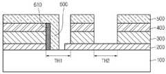
도 1은 실시예에 따른 태양전지를 도시한 평면도이고, 도 2는 도 1에서 A-A'선을 따라서 절단한 단면을 도시한 단면도이다.1 is a plan view illustrating a solar cell according to an embodiment, and FIG. 2 is a cross-sectional view illustrating a cross section taken along line AA ′ of FIG. 1.
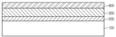
도 1 및 도 2를 참조하면, 실시예에 따른 태양전지는 지지 기판(100), 후면 전극층(200), 광 흡수층(300), 버퍼층(400), 전면 전극층(500), 접속 배선(600) 및 측면 절연부(610)를 포함한다.1 and 2, a solar cell according to an embodiment includes a
상기 지지 기판(100)은 플레이트 형상을 가지며, 상기 후면 전극층(200), 상기 광 흡수층(300), 상기 버퍼층(400), 상기 전면 전극층(500), 상기 접속 배선(600) 및 상기 측면 절연부(610)를 지지한다.The
상기 지지 기판(100)은 절연체일 수 있다. 상기 지지 기판(100)은 유리기판, 플라스틱기판 또는 금속기판일 수 있다. 더 자세하게, 상기 지지 기판(100)은 소다 라임 글래스(soda lime glass) 기판일 수 있다. 상기 지지 기판(100)은 투명할 수 있다. 또한, 상기 지지 기판(100)은 리지드하거나 플렉서블할 수 있다.The
상기 후면 전극층(200)은 도전층이다. 상기 후면 전극층(200)은 상기 지지 기판(100) 상에 배치된다.The
상기 후면 전극층(200)은 몰리브덴(Mo), 금(Au), 알루미늄(Al), 크롬(Cr), 텅스텐(W) 및 구리(Cu) 중 적어도 하나를 포함할 수 있다. 이 가운데, 몰리브덴(Mo)은 다른 원소에 비해 상기 지지기판(100)과 열팽창 계수의 차이가 적기 때문에 접착성이 우수하여 박리현상이 발생하는 것을 방지할 수 있고, 상술한 후면 전극층(200)에 요구되는 특성을 전반적으로 충족시킬 수 있다.The
상기 광 흡수층(300)은 상기 후면 전극층(200) 상에 배치된다.The light absorbing
상기 광 흡수층(300)은 Ⅰ-Ⅲ-Ⅳ족계 화합물을 포함한다. 예를 들어, 상기 광 흡수층(300)은 구리-인듐-갈륨-셀레나이드계(Cu(In,Ga)Se2;CIGS계) 결정 구조, 구리-인듐-셀레나이드계 또는 구리-갈륨-셀레나이드계 결정 구조를 가질 수 있다. 또한, 상기 광 흡수층(300)의 에너지 밴드갭(band gap)은 약 1 eV 내지 약 1.8 Ev 일 수 있다.The light absorbing
상기 버퍼층(400)은 상기 광 흡수층(300) 상에 배치된다. 본 발명과 같은 태양전지는 p형 반도체인 CIGS 또는 CIGSS 화합물 박막의 광 흡수층(300)과 n형 반도체인 전면 전극층(500) 박막간에 pn 접합을 형성한다. 하지만 두 물질은 격자상수와 밴드갭 에너지의 차이가 크기 때문에 양호한 접합을 형성하기 위해서는 밴드갭이 두 물질의 중간에 위치하는 버퍼층이 필요하다. 상기 버퍼층(400)은 황화 카드뮴(CdS)를 포함하며, 상기 버퍼층(400)의 에너지 밴드갭은 약 2.2eV 내지 2.4eV이다.The
도면에는 도시되지 않았지만, 상기 버퍼층 상에는 고저항 버퍼층이 더 배치될 수 있다. 상기 고저항 버퍼층은 불순물이 도핑되지 않은 징크 옥사이드(i-ZnO)를 포함할 수 있다. 상기 고저항 버퍼층의 에너지 밴드갭은 약 3.1eV 내지 3.3eV이다.Although not shown in the drawings, a high resistance buffer layer may be further disposed on the buffer layer. The high-resistance buffer layer may include zinc oxide (i-ZnO) that is not doped with impurities. The energy bandgap of the high resistance buffer layer is about 3.1 eV to 3.3 eV.
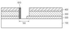
또한, 상기 버퍼층(400)에는 제 1 관통홈들(TH1)이 형성될 수 있다. 상기 제 1 관통홈들(TH1)은 상기 지지 기판(100)의 상면 및 상기 후면 전극층(200)의 상면을 노출하는 오픈 영역이다. 상기 제 1 관통홈들(TH1)은 평면에서 보았을 때, 일 방향으로 연장되는 형상을 가질 수 있다. 상기 제 1 관통홈들(TH1)의 폭은 약 80㎛ 내지 200㎛ 있으나, 이에 제한되는 것은 아니다.In addition, first through holes TH1 may be formed in the
상기 제 1 관통홈들(TH1)에는 접속 배선(700) 및 측면 절연부(710)가 갤핍되어 형성될 수 있다. 이와 관련하여서는, 하기에서 언급할 접속 배선(700)과 함께 상세히 설명하도록 한다.The interconnection line 700 and the side insulation part 710 may be formed in the first through holes TH1 by a gap. In this regard, it will be described in detail with the connection wiring 700 to be described below.
상기 전면 전극층(500)은 상기 버퍼층(400) 상에 배치된다, 상기 전면 전극층(500)은 투명하며, 도전층이다. 상기 전면 전극층(500)은 산화물을 포함할 수 있다. 예를 들어, 상기 전면 전극층(500)은 징크 옥사이드(zinc oxide), 인듐 틴 옥사이드(indium tin oxide;ITO) 또는 인듐 징크 옥사이드(indium zinc oxide;IZO) 등을 포함할 수 있다. 또한, 상기 산화물은 알루미늄(Al), 알루미나(Al2O3), 마그네슘(Mg) 또는 갈륨(Ga) 등의 도전성 불순물을 포함할 수 있다. 더 자세하게, 상기 전면 전극층(500)은 알루미늄 도핑된 징크 옥사이드(Al doped zinc oxide;AZO) 또는 갈륨 도핑된 징크 옥사이드(Ga doped zinc oxide;GZO) 등을 포함할 수 있다.The
상기 접속 배선(600)은 상기 전면 전극층(500)과 일체로 형성된다. 즉, 상기 접속 배선(600)은 상기 전면 전극층(500)이 형성되는 과정과 동시에 형성될 수 있고, 상기 접속 배선(600)으로 사용되는 물질은 상기 전면 전극층(500)으로 사용되는 물질과 동일하다.The
상기 접속 배선(600)은 상기 제 1 관통홈들(TH1) 내측에 배치된다. 즉, 상기 접속 배선(600)은 상기 광 흡수층(300)을 관통하게 배치된다.The
상기 접속 배선(600)은 상기 전면 전극층(500)으로부터 하방으로 연장되며, 상기 후면 전극층(200)에 접속된다. 즉, 상기 접속 배선(600)은 상기 전면 전극층(500)과 상기 후면 전극층(200)을 전기적으로 연결할 수 있다.The
예를 들어, 상기 접속 배선(600)은 제 1 셀(C1)의 전면 전극으로부터 연장되어, 상기 제 1 셀(C1)과 인접한 제 2 셀(C2)의 후면 전극에 접속된다. 따라서, 상기 접속 배선(600)은 서로 인접하는 셀들을 연결한다. 더 자세하게, 상기 접속 배선(600)은 서로 인접하는 셀들(C1, C2...)에 각각 포함된 윈도우와 이면 전극을 연결하여 전류가 흐르게 된다.For example, the
상기 측면 절연부(610)는 상기 제 1 관통홈들(TH1)에서, 상기 지지 기판(100)의 상면을 노출하는 오픈 영역 상에 형성될 수 있다. 상기 측면 절연부(610)는 상기 접속 배선(600)중 어느 하나의 측면에 배치될 수 있다. 즉, 상기 측면 절연부(610)는 상기 후면 전극층(200), 상기 광 흡수층(300) 및 상기 버퍼층(400)의 측면과 직접 접촉되어 형성될 수 있다.The
상기 측면 절연부(610)는 상기 접속 배선(600)보다 저항이 높은 영역으로, 상기 접속 배선(600) 내의 전자가 상기 광흡수층(300)으로 이동하는 것을 방지할 수 있다. 또한, 상기 접속 배선(600) 내의 전자가 반대 방향의 후면 전극층(200)으로 이동하는 것을 방지할 수 있다. 즉, 실시예에 따른 태양 전지는 상기 측면 절연부(610)에 의하여 누설전류를 감소시킬 수 있다.The
상기 측면 절연부(610)는 상기 접속 배선(600)보다 높은 저항을 가진 물질이라면 특별히 제한 없이 사용 가능하다. 더 자세하게, 상기 측면 절연부(610)는 금속 산화물층, 무기 산화물층 또는 고분자 절연층을 포함할 수 있다. 또한, 상기 측면 절연부(610)의 폭은 약 1㎛ 내지 10㎛ 일 수 있으나, 이에 제한되지 않는다.The
상기 측면 절연부(610)는 상기 제 1 관통홈(TH1)에 갭필되어 형성될 수 있다. 즉, 상기 측면 절연부(610)는 상기 접속 배선(600)과 함께 상기 제 1 관통홈(TH1)에 갭필되어 형성될 수 있다. 예를 들어, 상기 측면 절연부(610)는 상기 제 1 관통홈(TH1)에 의해 노출되는 후면 전극층(200), 광 흡수층(300), 버퍼층(400)의 측면과 상기 접속 배선(600)의 측면 사이에 형성될 수 있다. 이에 따라, 상기 측면 절연부(610)는 상기 제 1 관통홈(TH1)에 의해 노출되는 후면 전극층(200)의 일부 즉, 후면 전극층(200)의 측면과도 직접 접촉될 수 있다.
The
이와 같이 실시예에 따른 태양 전지는 제 1 관통홈(TH1)의 측면, 또는, 상기 접속 배선(600)의 측면에 형성되는 측면 절연부(610)를 포함하는 태양 전지를 제공한다.As described above, the solar cell according to the embodiment provides a solar cell including a
또한, 실시예에 따른 태양 전지는 상기 제 1 관통홈(TH1)에 의해, 상기 후면 전극층(200)의 분리 및 상기 전면 전극층(500)과 상기 후면 전극층(200)을 연결할 수 있다.In addition, the solar cell according to the embodiment may be separated from the
즉, 종래 상기 후면 전극층(200)의 분리와 상기 전면 전극층(500)과 상기 후면 전극층(200)을 연결을 위한 관통홈(TH1)들을 각각 형성하였던 것과 비교하여, 태양 전지로서 작동할 수 없는 영역 즉, 데드존(dead zone) 영역을 감소할 수 있다.That is, compared to the conventional separation of the
따라서, 실시예에 따른 태양 전지 제조 방법은 공정을 단순화할 수 있어 공정 효율의 향상 및 공정 비용을 절감할 수 있고, 또한, 데드존 영역을 감소할 수 있어 태양 전지의 효율을 향상시킬 수 있다.Therefore, the solar cell manufacturing method according to the embodiment can simplify the process, improve the process efficiency and reduce the process cost, and also reduce the dead zone area, thereby improving the efficiency of the solar cell.
또한, 측면 절연부를 통해 후면 전극층과 전면 전극층을 효과적으로 단락할 수 있어 누설전류의 양을 감소시킬 수 있는 효과가 있다.
In addition, it is possible to effectively short-circuit the rear electrode layer and the front electrode layer through the side insulating portion has the effect of reducing the amount of leakage current.
도 3 내지 도 7은 실시예에 따른 태양전지의 제조 방법을 설명하는 단면도들이다. 본 제조 방법에 관한 설명은 앞서 설명한 실시예에 따른 태양전지에 대한 설명을 참고한다.3 to 7 are cross-sectional views illustrating a method of manufacturing the solar cell according to the embodiment. For a description of the manufacturing method refer to the description of the solar cell according to the above-described embodiment.
도 3을 참고하면, 지지 기판(100) 상에 후면 전극층(200)이 형성된다. 상기 후면 전극층(200)은 PVD(Physical Vapor Deposition) 또는 도금의 방법으로 형성될 수 있다.Referring to FIG. 3, the
이어서, 도 4를 참조하면, 상기 후면 전극층(200) 상에 광 흡수층(300) 및 버퍼층(400)을 형성할 수 있다.Subsequently, referring to FIG. 4, the
상기 광 흡수층(300)은 예를 들어, 구리, 인듐, 갈륨, 셀레늄을 동시 또는 구분하여 증발시키면서 구리-인듐-갈륨-셀레나이드계(Cu(In,Ga)Se2;CIGS계)의 광 흡수층(300)을 형성하는 방법과 금속 프리커서 막을 형성시킨 후 셀레니제이션(Selenization) 공정에 의해 형성시키는 방법이 폭넓게 사용되고 있다.The light
금속 프리커서 막을 형성시킨 후 셀레니제이션 하는 것을 세분화하면, 구리타겟, 인듐 타겟, 갈륨 타겟을 사용하는 스퍼터링 공정에 의해서, 상기 이면전극(200) 상에 금속 프리커서 막이 형성된다. 이후, 상기 금속 프리커서 막은 셀레이제이션(selenization) 공정에 의해서, 구리-인듐-갈륨-셀레나이드계(Cu(In,Ga)Se2;CIGS계)의 광 흡수층(300)이 형성된다.When the metal precursor film is formed and selenization is subdivided, a metal precursor film is formed on the
이와는 다르게, 상기 구리 타겟, 인듐 타겟, 갈륨 타겟을 사용하는 스퍼터링공정 및 상기 셀레니제이션 공정은 동시에 진행될 수 있다.이와는 다르게, 구리 타겟 및 인듐 타겟 만을 사용하거나, 구리 타겟 및 갈륨 타겟을 사용하는 스퍼터링 공정 및 셀레니제이션 공정에 의해서, CIS계 또는 CIG계 광 흡수층(300)이 형성될 수 있다.Alternatively, the sputtering process using the copper target, the indium target, and the gallium target and the selenization process may be performed simultaneously. Alternatively, the sputtering using only the copper target and the indium target, or using the copper target and the gallium target By the process and selenization process, the CIS-based or CIG-based
상기 버퍼층(400)은 상기 광 흡수층(300) 상에 황화 카드뮴이 화학 용액 증착법(chemical bath deposition;CBD)에 의해서 증착되어 형성될 수 있다. 또한, 상기 버퍼층(400) 상에 징크 옥사이드가 스퍼터링 공정 등에 의해서 증착되고, 고저항 버퍼층(500)이 형성될 수 있다.The
이어서, 도 5 내지 도 7을 참조하면, 상기 버퍼층, 상기 광 흡수층 및 상기 후면 전극층을 관통하는 제 1 관통홈(TH1)들이 형성된다. 상기 제 1 관통홈(TH1)들은 상기 지지 기판(100)의 일부와 상기 후면 전극층(200)의 일부를 노출하도록 형성될 수 있다.Subsequently, referring to FIGS. 5 to 7, first through holes TH1 penetrating the buffer layer, the light absorbing layer, and the back electrode layer are formed. The first through holes TH1 may be formed to expose a portion of the
이에 따라서, 상기 지지 기판 상에 다수 개의 이면 전극들이 형성될 수 있고, 상기 버퍼층 상에 형성되는 상기 전면 전극층과 상기 제 1 관통홈(TH1)에 의해 노출되는 후면 전극층(200)을 전기적으로 연결할 수 있다.Accordingly, a plurality of back electrodes may be formed on the support substrate, and the front electrode layer formed on the buffer layer and the
상기 제 1 관통홈들(TH1)은 팁 등의 기계적인 장치 또는 레이저 장치 등에 의해서 형성될 수 있으나, 이에 제한되지는 않는다.The first through holes TH1 may be formed by a mechanical device such as a tip or a laser device, but are not limited thereto.
상기 제 1 관통홈들(TH1)의 측면에는 측면 절연부(610)가 형성된다. 바람직하게는, 상기 측면 절연부(610)는 상기 제 1 관통홈(TH1)에 의해 노출되는 상기 버퍼층(400), 상기 광 흡수층(300) 및 상기 후면 전극층(200)의 측면과 직접 접촉되도록 형성될 수 있다. 이에 따라, 상기 버퍼층(400) 상에 배치되는 전면 전극층(500)의 전자가 상기 광흡수층(300) 또는 상기 후면 전극층(200)으로 이동하는 것을 방지할 수 있어 누설전류의 양을 감소시킬 수 있다.
상기 측면 절연부(610)는 잉크젯 방법, 또는 마스크를 이용하여 상기 제 1 관통홈(TH1)의 측면에 형성될 수 있으나, 이에 제한되지는 않는다. 또한, 상기 절연부를 형성하는 물질은 액상, 기상 또는 페이스트 형태를 모두 포함할 수 있다. 상기 측면 절연부(610)와 상기 접속 배선(600)은 순차적으로 형성될 수 있다.The
도 6 및 도 7을 참조하면, 상기 버퍼층(400) 상에 투명한 도전물질이 증착되어 전면 전극층(500)이 형성된다.6 and 7, a transparent conductive material is deposited on the
이와 함께, 상기 제 1 관통홈들(TH1)의 내측, 바람직하게는 상기 제 1 관통홈들(TH1)의 내측과 직접 접촉하는 상기 측면 절연부(610)의 측면과 직접 접촉되도록 투명한 도전 물질이 증착되어 접속 배선(600)이 형성된다.In addition, a transparent conductive material may be formed in direct contact with the side surface of the
상기 전면 전극층(500) 및 상기 접속 배선(600)은 무산소 분위기에서 상기 투명한 도전물질이 증착되어 형성될 수 있다. 더 자세하게, 상기 전면 전극층(500)은 산소를 포함하지 않는 불활성 기체 분위기에서 알루미늄이 도핑된 징크 옥사이드가 증착되어 형성될 수 있다.The
도 7을 참조하면, 광 흡수층(300), 버퍼층(400) 및 전면 전극층(500)의 일부가 제거되어, 제 2 관통홈들(TH2)이 형성된다. 이에 따라, 상기 전면 전극층(500)은 패터닝되어, 다수 개의 윈도우들 및 다수 개의 셀들(C1, C2...)이 정의된다. 상기 제 2 관통홈들(TH2)의 폭은 약 80㎛ 내지 200㎛ 일 수 있으나, 이에 제한되지 않는다.Referring to FIG. 7, portions of the
이와 같이 실시예에 따른 태양 전지 제조 방법은 제 1 관통홈(TH1)의 측면, 또는, 상기 접속 배선(600)의 측면에 형성되는 측면 절연부(610)를 포함하는 태양 전지를 제공한다. 또한, 실시예에 따른 태양 전지 제조 방법은 상기 제 1 관통홈(TH1)에 의해, 상기 후면 전극층(200)의 분리 및 상기 전면 전극층(500)과 상기 후면 전극층(200)을 연결할 수 있다.Thus, the solar cell manufacturing method according to the embodiment provides a solar cell including a
즉, 종래 상기 후면 전극층(200)의 분리와 상기 전면 전극층(500)과 상기 후면 전극층(200)을 연결을 위한 관통홈(TH1)들을 각각 형성하였던 것과 비교하여, 태양 전지로서 작동할 수 없는 영역 즉, 데드존(dead zone) 영역을 감소할 수 있다.That is, compared to the conventional separation of the
따라서, 실시예에 따른 태양 전지 제조 방법은 공정을 단순화할 수 있어 공정 효율의 향상 및 공정 비용을 절감할 수 있고, 또한, 데드존 영역을 감소할 수 있어 태양 전지의 효율을 향상시킬 수 있다. 또한, 측면 절연부를 통해 후면 전극층과 전면 전극층을 효과적으로 단락할 수 있어 누설전류의 양을 감소시킬 수 있는 효과가 있다.
Therefore, the solar cell manufacturing method according to the embodiment can simplify the process, improve the process efficiency and reduce the process cost, and also reduce the dead zone area, thereby improving the efficiency of the solar cell. In addition, it is possible to effectively short-circuit the rear electrode layer and the front electrode layer through the side insulating portion has the effect of reducing the amount of leakage current.
이상에서 실시예들에 설명된 특징, 구조, 효과 등은 본 발명의 적어도 하나의 실시예에 포함되며, 반드시 하나의 실시예에만 한정되는 것은 아니다. 나아가, 각 실시예에서 예시된 특징, 구조, 효과 등은 실시예들이 속하는 분야의 통상의 지식을 가지는 자에 의해 다른 실시예들에 대해서도 조합 또는 변형되어 실시 가능하다. 따라서 이러한 조합과 변형에 관계된 내용들은 본 발명의 범위에 포함되는 것으로 해석되어야 할 것이다.The features, structures, effects and the like described in the embodiments are included in at least one embodiment of the present invention and are not necessarily limited to only one embodiment. Furthermore, the features, structures, effects, and the like illustrated in the embodiments may be combined or modified with respect to other embodiments by those skilled in the art to which the embodiments belong. Therefore, it should be understood that the present invention is not limited to these combinations and modifications.
이상에서 실시예를 중심으로 설명하였으나 이는 단지 예시일 뿐 본 발명을 한정하는 것이 아니며, 본 발명이 속하는 분야의 통상의 지식을 가진 자라면 본 실시예의 본질적인 특성을 벗어나지 않는 범위에서 이상에 예시되지 않은 여러 가지의 변형과 응용이 가능함을 알 수 있을 것이다. 예를 들어, 실시예에 구체적으로 나타난 각 구성 요소는 변형하여 실시할 수 있는 것이다. 그리고 이러한 변형과 응용에 관계된 차이점들은 첨부된 청구 범위에 포함되는 것으로 해석되어야 할 것이다.While the present invention has been particularly shown and described with reference to exemplary embodiments thereof, it is to be understood that the invention is not limited to the disclosed exemplary embodiments, but, on the contrary, It will be understood that various modifications and applications are possible. For example, each component specifically shown in the embodiments can be modified and implemented. And differences relating to such modifications and applications should be construed as being included in the appended claims.
Claims (11)
Translated fromKorean상기 지지 기판 상에 배치되는 후면 전극층;
상기 후면 전극층 상에 배치되는 광 흡수층;
상기 광 흡수층 상에 배치되는 버퍼층;
상기 버퍼층 상에 배치되는 전면전극층;
상기 광 흡수층을 관통하며, 상기 후면 전극층과 상기 전면 전극층을 전기적으로 연결하는 접속 배선; 및
상기 접속 배선의 측면 중 어느 하나의 측면에 형성되는 측면 절연부를 포함하고,
상기 측면 절연부는 상기 후면 전극층, 상기 광 흡수층 및 상기 버퍼층의 일부와 직접 접촉하는 태양 전지.A support substrate;
A rear electrode layer disposed on the support substrate;
A light absorbing layer disposed on the rear electrode layer;
A buffer layer disposed on the light absorbing layer;
A front electrode layer disposed on the buffer layer;
A connection wire penetrating the light absorbing layer and electrically connecting the rear electrode layer and the front electrode layer; And
It includes a side insulating portion formed on any one side of the side of the connection wiring,
And the side insulation portion is in direct contact with a portion of the back electrode layer, the light absorbing layer, and the buffer layer.
상기 버퍼층은 상기 버퍼층, 상기 광수층 및 상기 후면 전극층을 관통하는 관통홈을 포함하고,
상기 접속 배선 및 상기 측면 절연부는 상기 관통홈 내에 갤핍되는 태양 전지.The method of claim 1,
The buffer layer includes a through hole penetrating the buffer layer, the light water layer, and the back electrode layer.
And the connection wiring and the side insulating part are formed in the through groove.
상기 측면 절연부는, 상기 관통홈들에 의해 노출되는 상기 후면 전극층, 상기 광 흡수층 및 상기 버퍼층의 측면과 직접 접촉하는 태양 전지.The method of claim 2,
The side insulating part is in direct contact with the side surface of the back electrode layer, the light absorbing layer and the buffer layer exposed by the through grooves.
상기 측면 절연부는 상기 후면 전극층, 상기 광 흡수층 및 상기 버퍼층의 측면과 상기 접속 배선의 측면 사이에 형성되는 태양 전지.The method of claim 1,
The side insulating portion is formed between the side of the back electrode layer, the light absorbing layer and the buffer layer and the side of the connection wiring.
상기 측면 절연부는 금속 산화물층, 무기 산화물층 또는 고분자 절연층을 포함하는 태양 전지.The method of claim 1,
The side insulating portion includes a metal oxide layer, an inorganic oxide layer or a polymer insulating layer.
상기 측면 절연부의 너비는 1㎛ 내지 10㎛ 인 태양 전지.The method of claim 1,
The width of the side insulating portion is 1㎛ 10㎛ solar cell.
상기 후면 전극층 상에 광 흡수층을 형성하는 단계;
상기 광 흡수층 상에 버퍼층을 형성하는 단계;
상기 버퍼층, 상기 광 흡수층 및 상기 후면 전극층을 관통하는 관통홈을 형성하는 단계;
상기 관통홈의 측면에 측면 절연부를 형성하는 단계; 및
상기 버퍼층 상에 접속 배선 및 전면 전극층을 형성하는 단계를 포함하는 태양 전지 제조 방법.Forming a back electrode layer on the support substrate;
Forming a light absorbing layer on the back electrode layer;
Forming a buffer layer on the light absorbing layer;
Forming a through hole penetrating the buffer layer, the light absorbing layer, and the back electrode layer;
Forming a side insulation on a side of the through groove; And
Forming a connection wiring and a front electrode layer on the buffer layer.
상기 측면 절연부는 상기 관통홈에 의해 노출되는 상기 버퍼층, 상기 광 흡수층 및 상기 후면 전극층의 측면과 직접 접촉되는 태양 전지 제조 방법.8. The method of claim 7,
The side insulating portion is in direct contact with the side surface of the buffer layer, the light absorbing layer and the back electrode layer exposed by the through groove.
상기 측면 절연부의 너비는 1㎛ 내지 10㎛ 인 태양 전지 제조 방법.8. The method of claim 7,
The width of the side insulating portion is 1㎛ 10㎛ solar cell manufacturing method.
상기 접속 배선은 상기 관통홈에 전면 전극 물질이 갤핍되어 형성되는 태양 전지 제조 방법.8. The method of claim 7,
The connection wiring is a solar cell manufacturing method is formed by the galvanic front electrode material in the through groove.
상기 측면 절연부는 상기 관통홈의 측면 중 어느 하나의 측면에 형성되는 태양 전지 제조 방법.8. The method of claim 7,
The side insulating portion is formed on any one side of the side of the through groove solar cell manufacturing method.
Priority Applications (4)
| Application Number | Priority Date | Filing Date | Title |
|---|---|---|---|
| KR1020120030969AKR20130109330A (en) | 2012-03-27 | 2012-03-27 | Solar cell and method of fabricating the same |
| CN201380023068.5ACN104272470B (en) | 2012-03-27 | 2013-03-27 | Solar cell and manufacturing method thereof |
| PCT/KR2013/002561WO2013147517A1 (en) | 2012-03-27 | 2013-03-27 | Solar cell and method of fabricating the same |
| US14/389,167US10134932B2 (en) | 2012-03-27 | 2013-03-27 | Solar cell and method of fabricating the same |
Applications Claiming Priority (1)
| Application Number | Priority Date | Filing Date | Title |
|---|---|---|---|
| KR1020120030969AKR20130109330A (en) | 2012-03-27 | 2012-03-27 | Solar cell and method of fabricating the same |
Publications (1)
| Publication Number | Publication Date |
|---|---|
| KR20130109330Atrue KR20130109330A (en) | 2013-10-08 |
Family
ID=49260695
Family Applications (1)
| Application Number | Title | Priority Date | Filing Date |
|---|---|---|---|
| KR1020120030969ACeasedKR20130109330A (en) | 2012-03-27 | 2012-03-27 | Solar cell and method of fabricating the same |
Country Status (4)
| Country | Link |
|---|---|
| US (1) | US10134932B2 (en) |
| KR (1) | KR20130109330A (en) |
| CN (1) | CN104272470B (en) |
| WO (1) | WO2013147517A1 (en) |
Cited By (3)
| Publication number | Priority date | Publication date | Assignee | Title |
|---|---|---|---|---|
| KR101460915B1 (en)* | 2013-12-06 | 2014-11-17 | 희성전자 주식회사 | Isolating method of multi-junction solar cells and the structure of multi-junction solar cell manufactured by the method |
| WO2017043805A1 (en)* | 2015-09-09 | 2017-03-16 | 주식회사 무한 | Thin film-type solar cell and method for manufacturing same |
| KR101880640B1 (en)* | 2017-04-26 | 2018-07-23 | 한국에너지기술연구원 | Solar cell and method of fabricating the same |
Families Citing this family (3)
| Publication number | Priority date | Publication date | Assignee | Title |
|---|---|---|---|---|
| NL2014040B1 (en)* | 2014-12-23 | 2016-10-12 | Stichting Energieonderzoek Centrum Nederland | Method of making a curent collecting grid for solar cells. |
| CN112786737A (en)* | 2021-01-26 | 2021-05-11 | 凯盛光伏材料有限公司 | CIGS thin-film solar cell module and scribing method thereof |
| EP4601018A1 (en)* | 2022-11-30 | 2025-08-13 | Contemporary Amperex Technology (Hong Kong) Limited | Thin-film solar cell and electric device |
Family Cites Families (10)
| Publication number | Priority date | Publication date | Assignee | Title |
|---|---|---|---|---|
| DE3727826A1 (en)* | 1987-08-20 | 1989-03-02 | Siemens Ag | SERIES-CONNECTED THIN-LAYER SOLAR MODULE MADE OF CRYSTAL SILICON |
| EP1357602A1 (en)* | 2002-03-19 | 2003-10-29 | Scheuten Glasgroep | Self-adjusting series connection of thin films and method of fabrication |
| JP4703433B2 (en)* | 2006-02-27 | 2011-06-15 | 三洋電機株式会社 | Photovoltaic device |
| CN100416863C (en)* | 2006-10-13 | 2008-09-03 | 中国科学院上海技术物理研究所 | Cheap Polysilicon Thin Film Solar Cells |
| TWI440198B (en)* | 2008-03-13 | 2014-06-01 | Nexpower Technology Corp | Thin film laminated solar cell and manufacturing method thereof |
| KR101000383B1 (en)* | 2008-06-30 | 2010-12-13 | 한국철강 주식회사 | Integrated thin film solar cell and manufacturing method thereof |
| KR101144808B1 (en) | 2008-09-01 | 2012-05-11 | 엘지전자 주식회사 | Manufacturing Method For Thin-Film Type Solar Cell And The Same thereof |
| KR101173344B1 (en)* | 2009-10-30 | 2012-08-10 | 엘지이노텍 주식회사 | Solar cell and mehtod of fabricating the same |
| KR101273066B1 (en) | 2009-10-30 | 2013-06-10 | (주)아모레퍼시픽 | Composition for Reducing Skin Pore Size or Secreting Sebum Containing flower extract of Potentilla chinensis |
| US9059347B2 (en)* | 2010-06-18 | 2015-06-16 | Semiconductor Energy Laboratory Co., Ltd. | Photoelectric conversion device and manufacturing method thereof |
- 2012
- 2012-03-27KRKR1020120030969Apatent/KR20130109330A/ennot_activeCeased
- 2013
- 2013-03-27USUS14/389,167patent/US10134932B2/enactiveActive
- 2013-03-27WOPCT/KR2013/002561patent/WO2013147517A1/enactiveApplication Filing
- 2013-03-27CNCN201380023068.5Apatent/CN104272470B/ennot_activeExpired - Fee Related
Cited By (3)
| Publication number | Priority date | Publication date | Assignee | Title |
|---|---|---|---|---|
| KR101460915B1 (en)* | 2013-12-06 | 2014-11-17 | 희성전자 주식회사 | Isolating method of multi-junction solar cells and the structure of multi-junction solar cell manufactured by the method |
| WO2017043805A1 (en)* | 2015-09-09 | 2017-03-16 | 주식회사 무한 | Thin film-type solar cell and method for manufacturing same |
| KR101880640B1 (en)* | 2017-04-26 | 2018-07-23 | 한국에너지기술연구원 | Solar cell and method of fabricating the same |
Also Published As
| Publication number | Publication date |
|---|---|
| CN104272470A (en) | 2015-01-07 |
| US10134932B2 (en) | 2018-11-20 |
| CN104272470B (en) | 2017-11-03 |
| WO2013147517A1 (en) | 2013-10-03 |
| US20150083208A1 (en) | 2015-03-26 |
Similar Documents
| Publication | Publication Date | Title |
|---|---|---|
| JP2013506991A (en) | Photovoltaic power generation apparatus and manufacturing method thereof | |
| US10134932B2 (en) | Solar cell and method of fabricating the same | |
| KR101114099B1 (en) | Solar cell apparatus and method of fabricating the same | |
| KR101168810B1 (en) | Solar cell apparatus and method of fabricating the same | |
| KR101241467B1 (en) | Solar cell and preparing method of the same | |
| KR20120012325A (en) | Photovoltaic device and its manufacturing method | |
| KR101349429B1 (en) | Photovoltaic apparatus | |
| KR101173419B1 (en) | Solar cell and method of fabricating the same | |
| KR101338610B1 (en) | Solar cell apparatus and method of fabricating the same | |
| KR101338615B1 (en) | Solar apparatus and method of fabricating the same | |
| KR101172186B1 (en) | Solar cell apparatus and method of fabricating the same | |
| KR101154663B1 (en) | Solar cell apparatus | |
| KR20130136739A (en) | Solar cell and method of fabricating the same | |
| KR101210162B1 (en) | Solar cell apparatus and method of fabricating the same | |
| KR101393743B1 (en) | Solar cell and method of fabricating the same | |
| KR101765922B1 (en) | Solar cell apparatus and method of fabricating the same | |
| KR101220015B1 (en) | Solar cell apparatus and method of fabricating the same | |
| KR20130059976A (en) | Solar cell and method of fabricating the same | |
| KR101210104B1 (en) | Solar cell apparatus | |
| KR20120022231A (en) | Solar cell apparatus and method of fabricating the same | |
| KR101382995B1 (en) | Solar cell and method of fabricating the same | |
| KR101081222B1 (en) | Solar cell aparatus | |
| KR101283237B1 (en) | Solar power unit | |
| KR101349571B1 (en) | Photovoltaic apparatus | |
| KR101349432B1 (en) | Photovoltaic apparatus and method of fabricating the same |
Legal Events
| Date | Code | Title | Description |
|---|---|---|---|
| A201 | Request for examination | ||
| PA0109 | Patent application | Patent event code:PA01091R01D Comment text:Patent Application Patent event date:20120327 | |
| PA0201 | Request for examination | ||
| E902 | Notification of reason for refusal | ||
| PE0902 | Notice of grounds for rejection | Comment text:Notification of reason for refusal Patent event date:20130705 Patent event code:PE09021S01D | |
| AMND | Amendment | ||
| PG1501 | Laying open of application | ||
| E601 | Decision to refuse application | ||
| PE0601 | Decision on rejection of patent | Patent event date:20140127 Comment text:Decision to Refuse Application Patent event code:PE06012S01D Patent event date:20130705 Comment text:Notification of reason for refusal Patent event code:PE06011S01I | |
| AMND | Amendment | ||
| PX0901 | Re-examination | Patent event code:PX09011S01I Patent event date:20140127 Comment text:Decision to Refuse Application Patent event code:PX09012R01I Patent event date:20130905 Comment text:Amendment to Specification, etc. | |
| PX0601 | Decision of rejection after re-examination | Comment text:Decision to Refuse Application Patent event code:PX06014S01D Patent event date:20140410 Comment text:Amendment to Specification, etc. Patent event code:PX06012R01I Patent event date:20140226 Comment text:Decision to Refuse Application Patent event code:PX06011S01I Patent event date:20140127 Comment text:Amendment to Specification, etc. Patent event code:PX06012R01I Patent event date:20130905 Comment text:Notification of reason for refusal Patent event code:PX06013S01I Patent event date:20130705 |