KR20130109319A - Semiconductor light emitting device, light emitting module and lighting device - Google Patents
Semiconductor light emitting device, light emitting module and lighting deviceDownload PDFInfo
- Publication number
- KR20130109319A KR20130109319AKR1020120030950AKR20120030950AKR20130109319AKR 20130109319 AKR20130109319 AKR 20130109319AKR 1020120030950 AKR1020120030950 AKR 1020120030950AKR 20120030950 AKR20120030950 AKR 20120030950AKR 20130109319 AKR20130109319 AKR 20130109319A
- Authority
- KR
- South Korea
- Prior art keywords
- light emitting
- wiring
- region
- emitting cell
- forming
- Prior art date
- Legal status (The legal status is an assumption and is not a legal conclusion. Google has not performed a legal analysis and makes no representation as to the accuracy of the status listed.)
- Ceased
Links
Images


Classifications
- H—ELECTRICITY
- H10—SEMICONDUCTOR DEVICES; ELECTRIC SOLID-STATE DEVICES NOT OTHERWISE PROVIDED FOR
- H10H—INORGANIC LIGHT-EMITTING SEMICONDUCTOR DEVICES HAVING POTENTIAL BARRIERS
- H10H20/00—Individual inorganic light-emitting semiconductor devices having potential barriers, e.g. light-emitting diodes [LED]
- H10H20/01—Manufacture or treatment
- H—ELECTRICITY
- H01—ELECTRIC ELEMENTS
- H01L—SEMICONDUCTOR DEVICES NOT COVERED BY CLASS H10
- H01L24/00—Arrangements for connecting or disconnecting semiconductor or solid-state bodies; Methods or apparatus related thereto
- H01L24/01—Means for bonding being attached to, or being formed on, the surface to be connected, e.g. chip-to-package, die-attach, "first-level" interconnects; Manufacturing methods related thereto
- H01L24/18—High density interconnect [HDI] connectors; Manufacturing methods related thereto
- H01L24/23—Structure, shape, material or disposition of the high density interconnect connectors after the connecting process
- H01L24/24—Structure, shape, material or disposition of the high density interconnect connectors after the connecting process of an individual high density interconnect connector
- H—ELECTRICITY
- H10—SEMICONDUCTOR DEVICES; ELECTRIC SOLID-STATE DEVICES NOT OTHERWISE PROVIDED FOR
- H10H—INORGANIC LIGHT-EMITTING SEMICONDUCTOR DEVICES HAVING POTENTIAL BARRIERS
- H10H20/00—Individual inorganic light-emitting semiconductor devices having potential barriers, e.g. light-emitting diodes [LED]
- H10H20/80—Constructional details
- H10H20/81—Bodies
- H10H20/813—Bodies having a plurality of light-emitting regions, e.g. multi-junction LEDs or light-emitting devices having photoluminescent regions within the bodies
- H—ELECTRICITY
- H10—SEMICONDUCTOR DEVICES; ELECTRIC SOLID-STATE DEVICES NOT OTHERWISE PROVIDED FOR
- H10H—INORGANIC LIGHT-EMITTING SEMICONDUCTOR DEVICES HAVING POTENTIAL BARRIERS
- H10H20/00—Individual inorganic light-emitting semiconductor devices having potential barriers, e.g. light-emitting diodes [LED]
- H10H20/80—Constructional details
- H10H20/84—Coatings, e.g. passivation layers or antireflective coatings
- H—ELECTRICITY
- H10—SEMICONDUCTOR DEVICES; ELECTRIC SOLID-STATE DEVICES NOT OTHERWISE PROVIDED FOR
- H10H—INORGANIC LIGHT-EMITTING SEMICONDUCTOR DEVICES HAVING POTENTIAL BARRIERS
- H10H20/00—Individual inorganic light-emitting semiconductor devices having potential barriers, e.g. light-emitting diodes [LED]
- H10H20/80—Constructional details
- H10H20/85—Packages
- H10H20/852—Encapsulations
- H10H20/853—Encapsulations characterised by their shape
- H—ELECTRICITY
- H10—SEMICONDUCTOR DEVICES; ELECTRIC SOLID-STATE DEVICES NOT OTHERWISE PROVIDED FOR
- H10H—INORGANIC LIGHT-EMITTING SEMICONDUCTOR DEVICES HAVING POTENTIAL BARRIERS
- H10H20/00—Individual inorganic light-emitting semiconductor devices having potential barriers, e.g. light-emitting diodes [LED]
- H10H20/80—Constructional details
- H10H20/85—Packages
- H10H20/857—Interconnections, e.g. lead-frames, bond wires or solder balls
- H—ELECTRICITY
- H10—SEMICONDUCTOR DEVICES; ELECTRIC SOLID-STATE DEVICES NOT OTHERWISE PROVIDED FOR
- H10H—INORGANIC LIGHT-EMITTING SEMICONDUCTOR DEVICES HAVING POTENTIAL BARRIERS
- H10H29/00—Integrated devices, or assemblies of multiple devices, comprising at least one light-emitting semiconductor element covered by group H10H20/00
- H10H29/10—Integrated devices comprising at least one light-emitting semiconductor component covered by group H10H20/00
- H10H29/14—Integrated devices comprising at least one light-emitting semiconductor component covered by group H10H20/00 comprising multiple light-emitting semiconductor components
- H10H29/142—Two-dimensional arrangements, e.g. asymmetric LED layout
- H—ELECTRICITY
- H10—SEMICONDUCTOR DEVICES; ELECTRIC SOLID-STATE DEVICES NOT OTHERWISE PROVIDED FOR
- H10H—INORGANIC LIGHT-EMITTING SEMICONDUCTOR DEVICES HAVING POTENTIAL BARRIERS
- H10H20/00—Individual inorganic light-emitting semiconductor devices having potential barriers, e.g. light-emitting diodes [LED]
- H10H20/01—Manufacture or treatment
- H10H20/034—Manufacture or treatment of coatings
- H—ELECTRICITY
- H10—SEMICONDUCTOR DEVICES; ELECTRIC SOLID-STATE DEVICES NOT OTHERWISE PROVIDED FOR
- H10H—INORGANIC LIGHT-EMITTING SEMICONDUCTOR DEVICES HAVING POTENTIAL BARRIERS
- H10H20/00—Individual inorganic light-emitting semiconductor devices having potential barriers, e.g. light-emitting diodes [LED]
- H10H20/01—Manufacture or treatment
- H10H20/036—Manufacture or treatment of packages
- H10H20/0364—Manufacture or treatment of packages of interconnections
- H—ELECTRICITY
- H10—SEMICONDUCTOR DEVICES; ELECTRIC SOLID-STATE DEVICES NOT OTHERWISE PROVIDED FOR
- H10H—INORGANIC LIGHT-EMITTING SEMICONDUCTOR DEVICES HAVING POTENTIAL BARRIERS
- H10H20/00—Individual inorganic light-emitting semiconductor devices having potential barriers, e.g. light-emitting diodes [LED]
- H10H20/80—Constructional details
- H10H20/83—Electrodes
- H10H20/831—Electrodes characterised by their shape
Landscapes
- Engineering & Computer Science (AREA)
- Computer Hardware Design (AREA)
- Microelectronics & Electronic Packaging (AREA)
- Power Engineering (AREA)
- Led Devices (AREA)
- Internal Circuitry In Semiconductor Integrated Circuit Devices (AREA)
Abstract
Description
Translated fromKorean본 발명은 반도체 발광장치에 관한 것으로서, 특히 복수의 발광셀이 배열된 구조를 갖는 반도체 발광장치 및 이를 포함한 발광모듈과 조명 장치에 관한 것이다.
The present invention relates to a semiconductor light emitting device, and more particularly, to a semiconductor light emitting device having a structure in which a plurality of light emitting cells are arranged, and a light emitting module and a lighting device including the same.
일반적으로, 반도체 발광다이오드(LED)는 출력 및 효율이나 신뢰성 측면에서 광원으로서 유익한 장점을 가지므로, 디스플레이 장치의 백라이트뿐만 아니라 다양한 조명장치를 위한 고출력, 고효율 광원으로서 적극적으로 연구 개발되고 있다.
In general, semiconductor light emitting diodes (LEDs) have advantageous advantages as light sources in terms of output, efficiency, and reliability, and thus are actively researched and developed as high power and high efficiency light sources for various lighting devices as well as backlights of display devices.
이러한 LED를 조명용 광원으로 상용하기 위해서는 원하는 높은 수준의 출력을 제공하면서 광효율을 높이고 제조비용을 낮출 필요가 있다. 하지만, 고출력 발광 다이오드에서 동일 면적의 LED 칩에서 높은 광속을 얻기 위해서는 정격 전류를 높이는 경우에, 전류밀도의 증가로 인하여 오히려 광효율이 저하되고, 소자의 발열로 인하여 광효율 저하가 가속되는 문제가 있다.
In order to commercialize such LEDs as a light source for lighting, it is necessary to increase the light efficiency and lower the manufacturing cost while providing the desired high level output. However, in order to obtain a high luminous flux from an LED chip of the same area in a high output light emitting diode, when the rated current is increased, the light efficiency is lowered due to the increase of the current density, and the light efficiency is accelerated due to the heat generation of the device.
한편, 이러한 전류밀도의 문제를 낮추기 위해서 발광다이오드 칩의 면적을 증가시키는 방안을 고려할 수 있으나, 전체 면적에 균일한 전류밀도를 구현하기 어려우며, 높은 수율을 기대하기 어려운 문제가 있다.
On the other hand, in order to reduce the problem of the current density may be considered to increase the area of the light emitting diode chip, it is difficult to implement a uniform current density over the entire area, there is a problem that it is difficult to expect a high yield.
이러한 문제를 해결하기 위한 수단으로서 하나의 기판에서 성장된 LED를 위한 에피택셜층을 아이솔레이션 공정을 통해서 다수의 LED 셀로 구현하고, 이를 상호 연결하는 방안이 고려될 수 있다. 하지만, 이 경우에 적용되는 아이솔레이션 공정은 다수의 LED 셀의 상호 연결을 위한 메탈을 용이하게 증착하기 위해서 각 LED 셀의 경사면을 충분하게 완만하도록 형성할 필요가 있다. 하지만, 이 경우에 아이솔레이션 공정에서 제거되는 에피택셜층의 영역이 커지므로, 유효 발광면적(즉, 활성층 면적)이 현격하게 감소하는 문제가 있어 왔다.
As a means to solve this problem, a method of implementing an epitaxial layer for an LED grown on one substrate as a plurality of LED cells through an isolation process and interconnecting them may be considered. However, the isolation process applied in this case needs to be formed to sufficiently smooth the inclined surface of each LED cell in order to easily deposit metal for interconnecting a plurality of LED cells. However, in this case, since the area of the epitaxial layer removed in the isolation process becomes large, there has been a problem that the effective light emitting area (that is, the active layer area) decreases significantly.
따라서, 당 기술분야에서는, 아이솔레이션 공정에 의한 유효 발광면적의 감소를 최소화함으로써 광효율을 향상시킬 수 있는 멀티셀 반도체 발광 장치 및 제조방법과 그 응용 제품이 요구되고 있다.
Accordingly, there is a need in the art for a multi-cell semiconductor light emitting device, a manufacturing method, and an application product which can improve light efficiency by minimizing the reduction of the effective light emitting area by an isolation process.
본 발명의 일 측면은, 기판과, 상기 기판 상에 형성되며, 아이솔레이션 영역에 의해 분할되어 복수의 발광셀을 제공하는 반도체 적층체와, 상기 복수의 발광셀을 전기적으로 연결하는 배선부;를 포함하며, 상기 발광셀의 측면 중 상기 배선부가 형성된 영역은 상기 발광셀의 측면의 다른 영역보다 완만하게 경사진 것을 특징으로 하는 반도체 발광장치를 제공한다.
One aspect of the present invention includes a substrate, a semiconductor laminate formed on the substrate and divided by an isolation region to provide a plurality of light emitting cells, and a wiring unit for electrically connecting the plurality of light emitting cells. The area in which the wiring part is formed in the side surface of the light emitting cell is inclined more gently than the other area in the side surface of the light emitting cell.
상기 복수의 발광셀은 각각 복수의 측면을 가지며, 상기 배선부가 형성된 영역은 상기 발광셀의 적어도 하나의 측면 중 일부 영역일 수 있다.Each of the plurality of light emitting cells may have a plurality of side surfaces, and a region where the wiring part is formed may be a partial region of at least one side surface of the light emitting cell.
이 경우에, 상기 배선부가 형성된 영역에는 상기 다른 영역보다 완만한 경사면을 갖도록 오목한 홈부일 수 있다.
In this case, the region in which the wiring portion is formed may be a recessed portion having a gentle inclined surface than the other region.
상기 배선부가 형성된 영역에서 이루는 측면의 경사각은 상기 발광셀의 다른 측면영역에서 이루는 측면의 경사각보다 약 10°이상 작을 수 있다. 예를 들어, 상기 배선부가 형성된 영역에서 이루는 측면의 경사각은 40∼60°이며, 상기 발광셀의 다른 측면영역에서 이루는 측면의 경사각은 70°이상일 수 있다.
The inclination angle of the side surface formed in the region where the wiring portion is formed may be about 10 ° or less than the inclination angle of the side surface formed in the other side region of the light emitting cell. For example, the inclination angle of the side surface formed in the region where the wiring portion is formed may be 40 to 60 °, and the inclination angle of the side surface formed in the other side region of the light emitting cell may be 70 ° or more.
상기 반도체 적층체는 제1 및 제2 도전형 반도체층과 그 사이에 위치한 활성층을 포함할 수 있다.The semiconductor laminate may include first and second conductive semiconductor layers and an active layer disposed therebetween.
이 경우에, 상기 복수의 발광셀은 각각 상기 제1 및 제2 도전형 반도체층에 접속된 제1 및 제2 콘택을 포함하며, 상기 배선부는 상기 발광셀의 제1 및 제2 콘택 중 어느 하나에 연결된 서브 연결 배선과 상기 서브연결배선과 상기 제1 또는 제2 본딩패드를 연결하는 메인 연결 배선을 포함할 수 있다.In this case, the plurality of light emitting cells includes first and second contacts connected to the first and second conductivity type semiconductor layers, respectively, and the wiring portion is any one of the first and second contacts of the light emitting cells. The sub connection wires connected to the main connection wires may be connected to the sub connection wires and the first or second bonding pads.
상기 복수의 발광셀은 각각 복수의 제1 및 제2 콘택을 포함할 수 있다.
Each of the plurality of light emitting cells may include a plurality of first and second contacts.
특정 실시형태에서, 상기 아이솔레이션 영역의 저면에는 요철부가 형성될 수 있다.In a particular embodiment, an uneven portion may be formed on the bottom of the isolation region.
상기 배선부와 상기 발광셀의 원하지 않는 영역과의 전기적 접속이 방지되도록 상기 발광셀의 측면에 형성된 절연층을 포함할 수 있다.
It may include an insulating layer formed on the side of the light emitting cell to prevent electrical connection between the wiring portion and the unwanted region of the light emitting cell.
본 발명의 다른 측면은, 기판 상에 반도체 적층체를 형성하는 단계와, 상기 반도체 적층체가 상기 복수의 발광셀로 분리되도록 아이솔레이션 영역을 형성하는 단계와, 상기 발광셀의 측면 중 일부 영역은 상기 발광셀의 다른 측면보다 완만하게 경사진 배선영역을 형성하는 단계와, 적어도 일부가 상기 배선영역을 따라 위치하도록 상기 복수의 발광셀을 전기적으로 연결하는 배선부를 형성하는 단계를 포함하는 반도체 발광장치 제조방법을 제공한다.
Another aspect of the invention, forming a semiconductor laminate on a substrate, forming an isolation region so that the semiconductor laminate is separated into the plurality of light emitting cells, and a portion of the side surface of the light emitting cell is the light emission Forming a wiring area inclined more gently than the other side of the cell, and forming a wiring part for electrically connecting the plurality of light emitting cells so that at least a portion thereof is located along the wiring area. To provide.
상기 아이솔레이션 영역을 형성하는 단계와 상기 발광셀의 측면에 상기 배선영역을 형성하는 단계는 단일한 공정으로 수행될 수 있다.The forming of the isolation region and the forming of the wiring region on the side of the light emitting cell may be performed in a single process.
이 경우에, 상기 단일한 공정은 포토레지스트 공정을 이용하여 실행되며, 상기 포토레지스트 공정에서 사용되는 마스크는, 상기 배선영역에서 노광량이 점진적으로 변화되는 패턴을 가질 수 있다.
In this case, the single process is performed using a photoresist process, and the mask used in the photoresist process may have a pattern in which the exposure amount gradually changes in the wiring region.
배선부가 형성된 영역만을 다른 영역에 비해 경사지게 형성함으로써 셀간의 아이솔레이션 공정으로 인해 감소되는 유효 발광면적(예, 활성층)을 최소화할 수 있으며, 이로써 광효율을 향상시킬 수 있다.
By forming only the region where the wiring portion is formed to be inclined relative to other regions, the effective light emitting area (eg, the active layer) reduced by the isolation process between cells can be minimized, thereby improving the light efficiency.
덧붙여 상기한 과제의 해결수단 및 효과는, 본 발명의 특징을 모두 열거한 것은 아니다. 본 발명의 다양한 특징과 그에 따른 장점과 효과는 아래의 구체적인 실시형태를 참조하여 보다 상세하게 이해될 수 있을 것이다.
In addition, the solutions and effects of the above-mentioned problems do not list all the features of the present invention. The various features of the present invention and the advantages and effects thereof will be more fully understood by reference to the following specific embodiments.
도1은 본 발명의 일 실시형태에 따른 반도체 발광장치를 나타내는 평면도이다.
도2는 도1에 도시된 반도체 발광장치의 등가회로도이다.
도3은 도1에 도시된 반도체 발광장치의 발광셀간 연결을 확대하여 나타내는 평면도이다.
도4는 도3에 도시된 부분을 X1-X1'선을 따라 절개한 측단면도이다.
도5는 도3에 도시된 부분을 X2-X2'선을 따라 절개한 측단면도이다.
도6은 종래 기술에 따른 발광셀의 예를 나타내는 평면도이다.
도7은 본 발명의 다른 실시형태에 따른 반도체 발광장치를 나타내는 평면도이다.
도8은 도7에 도시된 반도체 발광장치의 등가회로도이다.
도9는 본 발명에 따른 반도체 발광장치 제조방법에 채용될 수 있는 마스크의 일 예를 나타내는 평면도이다.
도10은 도9에 도시된 마스크에 의한 노광량 분포를 나타내는 그래프이다.
도11 내지 도13은 본 발명에 따른 반도체 발광장치 제조방법에 채용가능한 포토레지스트의 패터닝 공정을 설명하기 위한 공정 단면도이다.
도14 및 도15는 각각 본 발명의 일 실시형태에 따른 반도체 발광장치를 갖는 조명장치를 나타내는 분해 사시도 및 개략 사시도(조립후 상태)이다.1 is a plan view showing a semiconductor light emitting device according to an embodiment of the present invention.
FIG. 2 is an equivalent circuit diagram of the semiconductor light emitting device shown in FIG.
3 is an enlarged plan view illustrating the connection between light emitting cells of the semiconductor light emitting device of FIG. 1.
4 is a side cross-sectional view of the portion shown in FIG. 3 taken along the line X1-X1 '.
FIG. 5 is a side cross-sectional view of the portion shown in FIG. 3 taken along the line X2-X2 '. FIG.
6 is a plan view showing an example of a light emitting cell according to the prior art.
7 is a plan view showing a semiconductor light emitting device according to another embodiment of the present invention.
FIG. 8 is an equivalent circuit diagram of the semiconductor light emitting device shown in FIG.
9 is a plan view illustrating an example of a mask that may be employed in the method of manufacturing a semiconductor light emitting device according to the present invention.
FIG. 10 is a graph showing the exposure amount distribution by the mask shown in FIG.
11 to 13 are cross-sectional views illustrating a process of patterning a photoresist that can be employed in the method of manufacturing a semiconductor light emitting device according to the present invention.
14 and 15 are an exploded perspective view and a schematic perspective view (post-assembly state) showing a lighting device having a semiconductor light emitting device according to an embodiment of the present invention, respectively.
이하, 첨부된 도면을 참조하여 본 발명의 실시형태를 상세히 설명하기로 한다.Hereinafter, embodiments of the present invention will be described in detail with reference to the accompanying drawings.
도1은 본 발명의 일 실시형태에 따른 반도체 발광장치를 나타내는 평면도이며, 도2는 도1에 도시된 반도체 발광장치의 등가회로도이다.
FIG. 1 is a plan view showing a semiconductor light emitting device according to an embodiment of the present invention, and FIG. 2 is an equivalent circuit diagram of the semiconductor light emitting device shown in FIG.
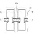
도1에 도시된 바와 같이, 본 실시형태에 따른 반도체 발광장치(50)는, 기판(51)과, 상기 기판(51) 상면에 형성된 복수의 발광셀(C)을 포함한다.As shown in FIG. 1, the semiconductor
상기 복수의 발광셀(C)은 6×9로 배열되며, 도4 및 도5에 도시된 바와 같이, 상기 기판(51) 상면에 순차적으로 형성된 제1 도전형 반도체층(52a), 활성층(52b) 및 제2 도전형 반도체층(52c)을 갖는 반도체 적층체(52)를 분리하여 얻어질 수 있다.The plurality of light emitting cells C are arranged in 6 × 9, and as shown in FIGS. 4 and 5, the first
본 실시형태에서, 상기 발광셀(C)은 도2의 등가회로도에 나타난 바와 같이 6개의 열로 배열된다. 또한, 각 열은 서로 직렬로 연결된 3개의 발광셀(C)이 3개씩 열결된 배열을 갖는다. 상기 반도체 발광장치(50)는 서로 직렬로 연결된 3개의 발광셀(C)이 모두 병렬로 연결되도록 배선부(56)를 갖는다. 상기 배선부(56)는 제1 및 제2 본딩패드(59a,59b)에 연결된다.
In the present embodiment, the light emitting cells C are arranged in six columns as shown in the equivalent circuit diagram of FIG. In addition, each column has an arrangement in which three light emitting cells C connected in series are thermally connected three by three. The semiconductor
본 실시형태에 채용되는 배선부(56)는, 상기 발광셀(C)에 직접 접속된 서브 연결 배선(56a)과 상기 서브 연결 배선(56a)의 일부와 상기 제1 및 제2 본딩패드(59a,59b)에 연결하는 메인 연결 배선(56b)을 포함할 수 있다. 도1에 도시된 바와 같이, 배선부(56)에 의해서 서로 직렬로 연결된 3개의 발광셀(C)은 모두 병렬로 연결될 수 있다(도2의 등가회로도 참조).The
상기 제1 및 제2 본딩패드(59a,59b)는 이에 한정되지는 않으나, Cr/Au와 같은 공지된 금속/합금층으로 형성될 수 있다. 상기 배선부(56)는 반사율이 우수하면서 전도성이 좋은 Al, Ag와 같은 금속으로 형성될 수 있다.
The first and
이러한 LED 셀의 배열과 배선부 구조는 원하는 전압규격 및 출력과 같은 요구에 따라 다양하게 변형될 수 있다. 예를 들어, 반도체 발광장치의 전압규격은 각 발광셀의 구동전압과 직렬로 연결되는 발광셀의 개수로 선택함으로써 설계할 수 있으며, 발광셀의 단위 출력과 총 구동되는 발광셀의 개수를 조절하여 원하는 출력을 얻을 수 있다.
The arrangement and wiring structure of the LED cell may be variously modified according to requirements such as desired voltage specifications and outputs. For example, the voltage specification of the semiconductor light emitting device may be designed by selecting the number of light emitting cells connected in series with the driving voltage of each light emitting cell, and by adjusting the unit output of the light emitting cells and the total number of light emitting cells driven. You can get the output you want.
본 실시형태에서, 상기 메인 연결 배선(56b)은 상기 기판(51) 상면(즉, 아이솔레이트된 영역)에 형성되므로, 비교적 평탄한 면에 형성된다. 반면에, 상기 서브 연결 배선(59a)은 아이솔레이트된 영역을 걸쳐서 상기 발광셀(C)에 연결되므로, 평탄하지 않은 경로를 따라 형성될 수 있다.In the present embodiment, the
구체적으로, 도3에 도시된 바와 같이, 상기 서브 연결 배선(59a)은 상기 기판(51) 상에 형성된 메인 연결부(59b)과 상기 발광셀(C)을 연결하거나, 상기 기판(51) 상면을 경유하여 인접한 발광셀(C)을 상호 연결하므로, 상기 발광셀(C)의 측면을 따라 형성된다.
Specifically, as shown in FIG. 3, the
이러한 비평탄한 면이 경사도가 심한 경우에는 배선증착공정이 어렵거나 단선과 같은 불량이 쉽게 발생하므로, 본 실시형태에서는 상기 발광셀(C)의 측면 중 상기 서브 연결 배선(56a)이 형성되는 영역은 선택적으로 완만한 경사를 갖도록 형성할 필요가 있다. 이에 대해서는 도3 내지 도5를 참조하여 보다 상세히 설명한다.
When the non-flat surface is inclined, the wiring deposition process is difficult or defects such as disconnection are easily generated. In this embodiment, the region where the
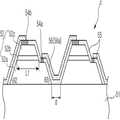
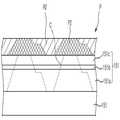
도4는 도3에 도시된 부분중 X1-X1'선을 따라 절개한 부분(배선 형성영역)의 측단면도를 나타내며, 도5는 도3에 도시된 부분중 X2-X2'선을 따라 절개한 부분의 측단면도를 나타낸다.FIG. 4 is a side cross-sectional view of a portion (wiring forming area) cut along the line X1-X1 'of the portion shown in FIG. 3, and FIG. 5 is cut along the line X2-X2' of the portion shown in FIG. The side cross-sectional view of a part is shown.
도5와 함께 도4를 참조하면, 본 실시형태에 채용된 발광셀(C)은 제1 및 제2 도전형 반도체층(52a,52c)에 각각 접속된 제1 및 제2 콘택(54a,54b)과 상기 발광셀(C)의 측면에 형성된 절연층(55)을 포함할 수 있다. 상기 절연층(55)은 상기 서브 연결 배선(56a)와 상기 발광셀(C)의 원하지 않는 영역과의 전기적 접속을 방지할 수 있다.
Referring to Fig. 4 along with Fig. 5, the light emitting cells C employed in the present embodiment are the first and
도4와 도5를 비교하면, 상기 발광셀(C) 측면 중 상기 서브 연결 배선(56a)이 형성되는 영역(도4)이 다른 측면 영역(도5)보다 완만하게 경사진 것으로 확인할 수 있다.4 and 5, it can be seen that the region (FIG. 4) in which the
이러한 경사도는 상기 기판(51)의 상면과 이루는 경사각으로 표현되어 설명될 수 있다.Such inclination may be expressed and described as an inclination angle formed with the upper surface of the
본 실시형태에서는, 도4에 도시된 바와 같이, 배선형성영역은 제2 콘택(54b)에 인접한 측면영역과 메사 에칭된 부분에 형성된 제1 콘택(54a)에 인접한 측면영역으로 구분될 수 있다. 상기 각각의 측면 영역은 원활한 배선 증착 공정이 보장되고 단선과 같은 불량을 감소될 수 있도록 상대적으로 완만한 경사각(θ1,θ2)을 갖는다. 여기서, 상기 2개의 경사각(θ1,θ2)은 서로 다른 각도를 가질 수 있으나, 필요에 따라 동일하게 설정될 수도 있다.In this embodiment, as shown in Fig. 4, the wiring forming region can be divided into a side region adjacent to the
반면에, 도5에 도시된 바와 같이, 배선형성영역을 제외한 상기 발광셀의 다른 측면영역의 적어도 일부는 배선형성영역의 경사각(θ1,θ2)보다 큰 경사각(θ3)을 갖는다. 바람직하게, 배선 형성 영역을 제외한 다른 측면 영역 전체가 배선형성영역의 경사각(θ1,θ2)보다 큰 경사각(θ3)을 가질 수 있다. 이와 같이, 배선형성영역을 제외한 상기 발광셀(C)의 측면영역에서 가파른 경사각(θ3)은 상대적으로 큰 유효 발광 면적을 보장할 수 있다.
On the other hand, as shown in FIG. 5, at least a part of the other side region of the light emitting cell except for the wiring forming region has an inclination angle θ3 greater than the inclination angles θ1 and θ2 of the wiring forming region. Preferably, the entire other side region except for the wiring formation region may have an inclination angle θ3 greater than the inclination angles θ1 and θ2 of the wiring formation region. As such, the steep inclination angle θ3 in the side region of the light emitting cell C, except for the wiring forming region, may ensure a relatively large effective light emitting area.
이를 간단하게 살펴보면, 도4 및 5에 도시된 발광셀의 단면에 나타난 활성층(52b)의 길이만을 비교하더라도 상기 다른 영역에 나타난 활성층의 길이(L2)가 상기 배선 형성 영역에서의 단면에 나타난 활성층의 길이(L1)보다 큰 것을 확인할 수 있다.Briefly, even if only the length of the
이와 같이, 발광셀의 측면 중 배선형성영역을 선택적으로 완만한 경사를 갖도록 구현하고, 다른 영역은 가능한 가파른 경사각을 유지함으로써 유효발광면적을 충분히 확보할 수 있다. 이와 관련하여 도3 및 도6을 참조하여 보다 상세히 설명한다.In this way, the wiring forming region of the side surface of the light emitting cell is selectively implemented to have a gentle inclination, and the other region can sufficiently secure the effective light emitting area by maintaining the steepest possible inclination angle. This will be described in more detail with reference to FIGS. 3 and 6.
우선, 도3은 서브 연결 배선(56a)에 의해 상호 연결된 발광셀(C)의 평면도를 나타낸다. 여기서, ST 및 SB는 발광셀(C) 상단면 및 바닥면의 면적을 나타내며, Sa는 활성층(52b)의 면적을 나타낸다.First, FIG. 3 shows a plan view of the light emitting cells C interconnected by the
앞서 설명한 바와 같이, 서브 연결 배선(56a)이 형성되는 영역에서는 완만한 경사각을 갖도록 추가적으로 에칭이 진행되며 이러한 과정에서 배선을 형성하기 위한 적절한 경사조건을 만족시킬 수 있으나, 일부 활성층이 불가피하게 제거된다.As described above, in the region where the
이러한 점을 감안하여, 본 실시형태에서는 완만한 경사면을 배선형성영역에 제한하고, 다른 측면영역은 상대적으로 큰 경사각(θ1)을 갖도록 형성함으로써 활성층(52b)의 제거 면적을 감소시키는 방안을 제공한다.In view of this, the present embodiment provides a method of reducing the removal area of the
도6은 비교예로서 본 실시형태와 달리 전체 측면을 완만한 경사각으로 형성한 셀의 평면도를 나타낸다. 여기서, S'T 및 S'B는 발광셀 상단면 및 바닥면의 면적이며, S'a는 배선 공정을 필요한 완만한 경사면을 갖도록 모든 측면을 가공할 발광셀에서의 활성층의 면적을 나타낸다. 본 비교예에 따른 활성층 면적(S'a)을 도3과 유사하게 배선형성영역만을 선택적으로 완만하게 가공할 경우에 활성층의 면적(Sa)하면, 본 실시형태의 활성층이 상당한 크기로 더 큰 면적을 가짐을 확인할 수 있다.Fig. 6 shows a plan view of a cell in which all sides are formed at a gentle inclination angle, unlike the present embodiment as a comparative example. Here, S 'T and S'B are the areas of the top surface and the bottom surface of the light emitting cell, and S 'a represents the area of the active layer in the light emitting cell to be processed on all sides so as to have a gentle inclined surface for the wiring process. When active area according to the comparative example (S'a) the area of the active layer in the case similarly selective gradually processed into only the wiring formation region and Fig. 3 (Sa), this embodiment of the active layer is larger in sizable It can be confirmed that it has an area.
이와 같이, 본 실시형태에 따르면, 배선형성영역에서 완만한 경사를 갖도록 구현하여 배선의 불량을 최소화하면서 동시에, 다른 영역에서는 상대적으로 높은 경사각을 갖도록 구현함으로써 배선 공정에 필요한 완만한 경사로 발광셀의 전체 측면을 가공하는 형태에서 보다 큰 활성층 면적을 제공할 수 있다.
As described above, according to the present exemplary embodiment, the slanted slope is minimized in the wiring forming region to minimize the defect of the wiring and at the same time, the slanted slope is required for the wiring process. Larger active layer areas can be provided in the form of side processing.
상기 배선부(56)가 형성된 영역에서 이루는 측면의 경사각(θ1,θ2)은 상기 발광셀(C)의 다른 측면영역에서 이루는 측면의 경사각(θ3)보다 약 10°이상 작을 수 있다. 예를 들어, 상기 배선부(56)가 형성된 영역에서 이루는 측면의 경사각(θ1,θ2)은 40∼60°이며, 상기 발광셀(C)의 다른 측면영역에서 이루는 측면의 경사각(θ3)은 70°이상일 수 있으며, 물론 이상적으로는 수직인 각을 포함할 수 있다.
The inclination angles θ1 and θ2 of the side surface formed in the region where the
본 실시형태에서, 상기 배선형성영역에 완만한 경사를 갖도록 추가적으로 에칭된 부분은 추가적으로 에칭되지 않은 다른 영역에 비해 오목한 형상을 가지므로, 배선형성영역은 실제로 "오목한 홈부"로 이해될 수 있다.
In this embodiment, the portion additionally etched to have a gentle inclination to the wiring forming region has a concave shape compared to other regions which are not additionally etched, so that the wiring forming region can actually be understood as a “concave groove portion”.
본 발명은 발광셀의 배열뿐만 아니라 다른 특징적인 요소를 포함한 다양한 실시형태로 구현될 수 있다. 이러한 실시형태는 도7에 예시되어 있다.
The present invention can be implemented in various embodiments including not only the arrangement of the light emitting cells but also other characteristic elements. This embodiment is illustrated in FIG.
도7에 도시된 반도체 발광장치(100)는, 기판(101)과, 상기 기판(101) 상면에 세로 방향으로 배열된 4개의 발광셀(C)을 포함한다.The semiconductor
본 실시형태에 채용된 발광셀도 앞선 실시형태와 유사하게, 상기 기판(101) 상면에 순차적으로 형성된 제1 도전형 반도체층, 활성층 및 제2 도전형 반도체층을 갖는 반도체 적층체를 포함할 수 있다. 다만, 도7에 도시된 발광셀(C)은, 도1에 도시된 발광셀과 달리, 각각 5개의 제1 및 제2 콘택을 포함하는 구조를 갖는다.Similar to the previous embodiment, the light emitting cell employed in the present embodiment may also include a semiconductor laminate having a first conductive semiconductor layer, an active layer, and a second conductive semiconductor layer sequentially formed on the upper surface of the
이와 같이, 본 발명에서 다양한 형태의 발광셀이 사용될 수 있다. 예를 들어, 도1에 도시된 바와 같이, 아이솔레이션 영역으로는 물리적으로 구분된 하나의 발광셀이 각각 하나의 제1 및 제2 콘택을 포함하며, 실제 구동시에 단일한 발광요소로 구동할 수도 있으며, 본 실시형태와 같이, 물리적으로 구분된 하나의 발광셀에서 일정한 간격으로 복수개의 제1 및 제2 콘택을 구비하여 실제 복수개의 발광요소와 같이 구동할 수 있다.
As such, various types of light emitting cells may be used in the present invention. For example, as illustrated in FIG. 1, one physically divided light emitting cell includes one first and second contacts, and may be driven as a single light emitting element in actual driving. As in the present embodiment, the plurality of first and second contacts may be provided at a predetermined interval in one physically divided light emitting cell to be driven like a plurality of light emitting elements.
그 결과, 물리적으로 분리된 4개의 발광셀이 직렬로 연결된 형태를 가지만, 일정한 간격을 갖는 5개의 콘택에 의해 동일한 발광셀에서 각각 5개의 발광요소로 작용하며, 그 구동회로는 도8에 도시된 바와 같이, 6×4의 배열로 이해될 수 있다.
As a result, the four physically separated light emitting cells have a form connected in series, but each of the five light emitting elements in the same light emitting cell is operated by five contacts having a constant interval, and the driving circuit shown in FIG. As can be understood in an array of 6 × 4.
본 실시형태에 채용된 배선부(106)는, 상기 발광셀(C)에 직접 접속된 서브 연결 배선(106a)과 상기 서브 연결 배선(106a)의 일부와 제1 및 제2 본딩패드(109a,109b)에 연결하는 메인 연결 배선(106b)을 포함할 수 있다.The
앞선 실시형태와 유사하게, 발광셀(C)의 측면 중 서브 연결 배선(106a)가 형성되는 배선형성영역은 원활한 배선증착공정을 보장하고, 단선과 같은 불량을 감소시킬 수 있는 정도의 상대적으로 완만한 경사각을 갖는다. 반면에, 배선형성영역을 제외한 다른 측면영역의 적어도 일부는 배선형성영역의 경사각보다 큰 경사각을 갖는다.Similar to the previous embodiment, the wiring forming region in which the
이와 같이, 배선형성영역을 제외한 상기 발광셀(C)의 측면영역에서 갖는 가파른 경사각은 상대적으로 큰 유효 발광 면적을 보장할 수 있다.As such, the steep inclination angle of the side surface of the light emitting cell C, except for the wiring forming region, may ensure a relatively large effective light emitting area.
한편, 본 실시형태에서는, 아이솔레이션으로 노출된 기판(101) 상면에 다수의 요철(P)이 형성된다. 이러한 요철을 통해서 광추출효율을 개선할 수 있다.
On the other hand, in this embodiment, many unevenness | corrugation P is formed in the upper surface of the board |
상술한 바와 같이, 배선형성영역에서는 완만한 경사를 갖도록 구현하여 배선의 불량을 최소화하면서 동시에, 다른 영역에서는 상대적으로 높은 경사각을 갖도록 구현함으로써 배선 공정에 필요한 완만한 경사로 발광셀의 전체 측면을 가공하는 경우보다 큰 활성층 면적을 제공할 수 있다.
As described above, in order to minimize the defect of the wiring by implementing a gentle inclination in the wiring forming region, and to implement a relatively high inclination angle in other areas, to process the entire side surface of the light emitting cell with a gentle inclination necessary for the wiring process It can provide a larger active layer area than in the case.
이러한 배선형성영역에 선택적으로 완만한 경사구조를 채용하는 공정은 기존의 아이솔레이션 공정 및/또는 메사에칭공정과 별도로 구현될 수 있으나, 이러한 일련의 공정을 단일한 포토레지스트 공정을 통해서 보다 용이하게 구현될 수 있다.
The process of selectively adopting a gentle inclined structure in the wiring forming region may be implemented separately from the existing isolation process and / or mesa etching process, but such a series of processes may be more easily implemented through a single photoresist process. Can be.
예를 들어, 포토레지스트 공정에서 사용되는 마스크를 노광량이 점진적으로 조절되도록 개량함으로써 배선형성영역에 선택적으로 원하는 경사도를 구현할 수 있다. 도9에 도시된 마스크는 본 제조방법에 채용될 수 있는 마스크의 일 예이다.
For example, the mask used in the photoresist process may be improved to gradually adjust the exposure amount to selectively implement a desired inclination in the wiring forming region. The mask shown in Fig. 9 is an example of a mask that can be employed in the present manufacturing method.
도9에 도시된 마스크(M)는 포지티브 포토레지스트 공정에 사용되는 마스크이며, 아이솔레이션 공정과 메사에칭공정과 함께 배선형성영역에 대한 경사면 형성 공정을 실시할 수 있다.The mask M shown in FIG. 9 is a mask used in a positive photoresist process, and an inclined plane forming process for the wiring formation region can be performed in addition to an isolation process and a mesa etching process.
상기 마스크(M) 사이의 영역은 발광셀을 분리하기 위한 아이솔레이션 영역으로 완전 노출되며, X2-X2'로 표시된 영역과 같이, 배선형성영역과 메사에칭영역과 관련 없는 발광셀 영역에서는 노광량이 차단된다.
The area between the masks M is completely exposed as an isolation area for separating the light emitting cells, and the exposure dose is blocked in the light emitting cell area not related to the wiring forming area and the mesa etching area, such as the area indicated by X2-X2 '. .
이와 달리, 메사에칭 영역과 함께 배선형성영역에서는 제1 및 제2 오픈패턴(OP1, OP2)을 이용하여 노광량을 조절함으로써 원하는 포토레지스트 패턴을 형성할 수 있다.In contrast, in the wiring forming region together with the mesa etching region, a desired photoresist pattern may be formed by adjusting exposure amounts using the first and second open patterns OP1 and OP2.
원하는 노광량의 조절은 오픈 패턴의 크기 및 수를 이용하여 적절히 조절할 수 있다. 예를 들어, 배선형성영역에 요구되는 경사면은 그 노광량이 점진적으로 변경되는 패턴을 채용함으로써 구현할 수 있다.The adjustment of the desired exposure amount can be appropriately adjusted using the size and number of open patterns. For example, the inclined surface required for the wiring forming region can be implemented by adopting a pattern in which the exposure amount is gradually changed.
본 예에서, 상기 제1 오픈패턴(OP1)은 메사에칭 영역과 함께 그 영역에 제공될 배선을 위한 경사면을 형성하기 위해서 사용된다. 제2 오픈패턴(OP2)은 제2 콘택에 연결될 배선을 위한 경사면을 형성하기 위해서 사용된다.,In this example, the first open pattern OP1 is used to form an inclined surface for wiring to be provided in the region together with the mesa etching region. The second open pattern OP2 is used to form an inclined surface for wiring to be connected to the second contact.
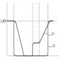
도10의 E2 곡선에 나타난 바와 같이, 상기 제1 오픈패턴(OP1)에 의한 노광량은 제1 콘택이 형성될 영역(d3-d4)에서는 일정하다가 발광셀의 가장자리로 갈수록(d4-d5) 증가하며, 상기 제2 오픈영역(OP2)에 의한 노광량은 발광셀의 가장자리로 갈수록(d2-d1) 증가한다.
As shown in the curve E2 of FIG. 10, the exposure amount by the first open pattern OP1 is constant in the region d3-d4 where the first contact is to be formed, and then increases toward the edge of the light emitting cell (d4-d5). The exposure amount of the second open area OP2 increases as the edge of the light emitting cell (d2-d1) increases.
이러한 마스크(M)를 이용하여 에칭공정에 사용될 포토레지스트 패턴 형성공정은 도11 내지 도13에 예시되어 있다.The photoresist pattern forming process to be used in the etching process using this mask M is illustrated in Figs.
도11에 도시된 바와 같이, 기판(151) 상에 제1 도전형 반도체층(151a), 활성층(151b) 및 제2 도전형 반도체층(151c)이 순차적으로 성장시켜 다수의 발광셀을 위한 반도체 적층체(151)를 형성하고, 상기 반도체 적층체(151) 상에 포토레지스트층(P)을 형성한다.
As shown in FIG. 11, the first
이어, 도9에 도시된 마스크를 이용하여 포토레지스트(P)를 노광시킨다. 앞서 설명한 바와 같이, X1-X1'로 절개된 부분과 X2-X2'로 절개된 부분은 서로 다른 형태로 노광되고 현상된 후에 얻어지는 포토레지스트 패턴이 상이해진다.
Next, the photoresist P is exposed using the mask shown in FIG. As described above, the portion cut into X1-X1 'and the portion cut into X2-X2' are different in the photoresist pattern obtained after exposure and development in different forms.
도12 및 도13은 각각 X1-X1' 및 X2-X2'로 절개된 부분에서 노광되고 현상한 후에 남겨질 포토레지스트 패턴(P1,P2)의 윤곽을 나타낸다.12 and 13 illustrate the contours of the photoresist patterns P1 and P2 to be left after exposure and development in portions cut into X1-X1 'and X2-X2', respectively.
도12에 도시된 바와 같이, 실제 노광된 영역(R1)에 제거된 후에 얻어지는 포토레지스트 패턴(P1)은 마스크의 가장자리에서 불가피하게 발생되는 노광에 의해 다소 경사진 면을 갖지만, 비교적 가파른 경사면을 제공한다.As shown in Fig. 12, the photoresist pattern P1 obtained after being removed in the actual exposed region R1 has a surface which is somewhat inclined by exposure inevitably generated at the edge of the mask, but provides a relatively steep inclined surface. do.
이에 반해 도13에 도시된 바와 같이, 실제 노광된 영역(R2)에 제거된 후에 얻어지는 포토레지스트 패턴(P2)은 점진적인 노광량의 조절로 인해, 메사에칭영역은 물론, 배선증착공정에 유리한 완만한 경사면을 제공할 수 있다.On the other hand, as shown in FIG. 13, the photoresist pattern P2 obtained after being removed in the actually exposed region R2 is gradually inclined to the mesa etching region as well as the wiring deposition process due to the gradual adjustment of the exposure amount. Can be provided.
도12 및 도13의 단면으로 정의되는 포토레지스트 패턴은 앞서 설명한 바와 같이, 노광공정 후에 적절한 현상과정을 통해서 얻어질 수 있다. 이어, 입체적으로 얻어진 포토레지스트 패턴을 이용하여 ICP 드라이 에칭과 같은 공지된 에칭공정을 이용하여 도12 및 도13에 표시된 "C"와 같은 형상의 발광셀을 얻을 수 있다.As described above, the photoresist pattern defined by the cross sections of FIGS. 12 and 13 may be obtained through an appropriate developing process after the exposure process. Subsequently, a light emitting cell having a shape such as "C" shown in FIGS. 12 and 13 can be obtained using a known etching process such as ICP dry etching using a three-dimensionally obtained photoresist pattern.
이와 같이, 측면 영역에 선택적으로 다른 경사각을 갖도록 발광셀을 형성하는 공정을 하나의 마스크를 이용하는 포토레지스트 공정과 에칭공정으로 용이하게 구현할 수 있다.
As such, the process of forming the light emitting cells to selectively have different inclination angles in the side regions may be easily implemented by a photoresist process and an etching process using one mask.
본 발명의 다양한 실시형태에 따른 멀티칩 어레이 반도체 발광장치는 인쇄회로기판과 같이 전극부를 갖는 기재를 포함하는 다양한 형태의 모듈에서 칩으로 유용하게 사용될 수 있다. 또한, 상술된 다양한 발광장치 및 발광 모듈은 구동부를 포함한 조명장치로 구현될 수 있다.
The multi-chip array semiconductor light emitting device according to various embodiments of the present invention may be usefully used as a chip in various types of modules including a substrate having an electrode portion, such as a printed circuit board. In addition, the above-described various light emitting devices and light emitting modules may be implemented as lighting devices including a driving unit.
도14 및 도15에는 본 발명에 따른 조명장치의 일 예로서 벌브형 램프가 예시되어 있다. 도14는 조명장치의 구성에 대한 이해가 용이하도록 각 구성요소를 분해한 상태의 사시도이며, 도15는 도14에서 분해된 구성요소가 조립된 상태(볼록렌즈형 커버의 결합 제외)를 나타내는 사시도이다.
14 and 15 illustrate a bulb type lamp as an example of the lighting apparatus according to the present invention. FIG. 14 is a perspective view of an exploded state of each component for easy understanding of the configuration of the lighting apparatus, and FIG. 15 is a perspective view illustrating a state in which the disassembled components are assembled in FIG. 14 (excluding the convex lens cover coupling). to be.
도14 및 도15를 참조하면, 상기 조명장치(300)는 발광모듈(350)과 구동부(330)와 외부접속부(310)를 포함한다. 또한, 외부 및 내부 하우징(340,320)과 커버부(360)와 같은 외형구조물을 추가적으로 포함할 수 있다.
14 and 15, the
상기 발광모듈(350)은 상술된 반도체 발광장치(355)와 그 발광장치(355)가 탑재된 회로기판(351)을 가질 수 있다. 본 실시형태에서는, 1개의 반도체 발광장치(355)가 상기 회로기판(351) 상에 실장된 형태로 예시되어 있으나, 필요에 따라 복수개로 장착될 수 있다.
The
본 실시형태에 따른 조명장치(300)에서는, 상기 발광모듈(350)은 열방출부로 작용하는 외부 하우징(340)을 포함할 수 있다. 상기 외부 하우징(340)은 상기 발광모듈(350)과 직접 접속하여 방열효과를 향상시키는 열방출판(345)을 포함할 수 있다. 또한, 상기 조명장치(300)는 발광모듈(350) 상에 장착되며 볼록한 렌즈형상을 갖는 커버부(360)를 포함할 수 있다.
In the
본 실시형태와 같이, 상기 구동부(330)는 내부 하우징(320)에 장착되어 소켓구조와 같은 외부접속부(310)에 연결되어 외부 전원으로부터 전원을 제공받을 수 있다.As in the present embodiment, the driving
또한, 상기 구동부(330)는 발광모듈(350)의 반도체 발광장치(355)를 구동시킬 수 있는 적정한 전류원으로 변환시켜 제공하는 역할을 한다. 예를 들어, 이러한 구동부(330)는 AC-DC 컨버터 또는 정류회로부품 등으로 구성될 수 있다.
In addition, the driving
이와 같이, 상술된 발광장치와 발광모듈은 램프와 같은 다양한 실내 조명장치, 가로등, 간판, 표지등과 같은 실외조명장치, 자동차, 항공기 및 선박용 헤드램프, 후방등과 같은 교동수단용 조명장치 등 다양하게 구현될 수 있다. 또한, 조명장치는 추가적으로 방열부재 및/또는 반사판 등의 구조를 포함할 수 있다.
As described above, the above-described light emitting device and the light emitting module may include various indoor lighting devices such as lamps, outdoor lighting devices such as street lamps, signs, signs, etc., lighting devices for moving means such as head lamps for automobiles, aircrafts and ships, and rear lights. Can be implemented. In addition, the lighting apparatus may further include a structure such as a heat dissipation member and / or a reflecting plate.
본 발명은 상술한 실시형태 및 첨부된 도면에 따라 한정되는 것이 아니고, 첨부된 청구범위에 따라 한정하고자 하며, 청구범위에 기재된 본 발명의 기술적 사상을 벗어나지 않는 범위 내에서 다양한 형태의 치환, 변형 및 변경이 가능하다는 것은 당 기술분야의 통상의 지식을 가진 자에게 자명할 것이다.The present invention is not limited to the above-described embodiment and the accompanying drawings, but is intended to be limited by the appended claims, and various forms of substitution, modification, and within the scope not departing from the technical spirit of the present invention described in the claims. It will be apparent to those skilled in the art that changes are possible.
Claims (25)
Translated fromKorean상기 기판 상에 형성되며, 아이솔레이션 영역에 의해 분할되어 복수의 발광셀을 제공하는 반도체 적층체; 및
상기 복수의 발광셀을 전기적으로 연결하는 배선부;를 포함하며,
상기 발광셀의 측면 중 상기 배선부가 형성된 영역은 상기 발광셀의 측면의 다른 영역보다 완만하게 경사진 것을 특징으로 하는 반도체 발광장치.
Board;
A semiconductor laminate formed on the substrate and divided by an isolation region to provide a plurality of light emitting cells; And
Includes; a wiring unit for electrically connecting the plurality of light emitting cells,
And a region in which the wiring portion is formed among side surfaces of the light emitting cell is inclined more gently than other regions of the side surface of the light emitting cell.
상기 복수의 발광셀은 각각 복수의 측면을 가지며,
상기 배선부가 형성된 영역은 상기 발광셀의 적어도 하나의 측면 중 일부 영역인 것을 특징으로 하는 반도체 발광장치.
The method of claim 1,
Each of the plurality of light emitting cells has a plurality of side surfaces,
And the area where the wiring part is formed is a part of at least one side surface of the light emitting cell.
상기 배선부가 형성된 영역에는 상기 다른 영역보다 완만한 경사면을 갖도록 오목한 홈부가 형성된 것을 특징으로 하는 반도체 발광장치.
The method according to claim 2, wherein
And a concave groove portion is formed in a region where the wiring portion is formed to have a gentle slope than the other region.
상기 배선부가 형성된 영역에서 이루는 측면의 경사각은 상기 발광셀의 다른 측면영역에서 이루는 측면의 경사각보다 약 10°이상 작은 것을 특징으로 하는 반도체 발광장치.
The method of claim 1,
And the inclination angle of the side surface formed in the region where the wiring portion is formed is about 10 ° or less than the inclination angle of the side surface formed in the other side region of the light emitting cell.
상기 배선부가 형성된 영역에서 이루는 측면의 경사각은 40∼60°이며,
상기 발광셀의 다른 측면영역에서 이루는 측면의 경사각은 70°이상인 것을 특징으로 하는 반도체 발광장치.
5. The method of claim 4,
The inclination angle of the side surface formed in the area where the wiring portion is formed is 40 to 60 °,
The inclination angle of the side surface formed in the other side region of the light emitting cell is 70 ° or more.
상기 반도체 적층체는 제1 및 제2 도전형 반도체층과 그 사이에 위치한 활성층을 포함하는 것을 특징으로 하는 반도체 발광장치.
The method of claim 1,
The semiconductor laminate includes a first and a second conductivity type semiconductor layer and an active layer disposed therebetween.
상기 복수의 발광셀은 각각 상기 제1 및 제2 도전형 반도체층에 접속된 제1 및 제2 콘택을 포함하며, 상기 반도체 발광장치는 제1 및 제2 본딩패드를 더 포함하며,
상기 배선부는 상기 발광셀의 제1 및 제2 콘택 중 어느 하나에 연결된 서브 연결 배선과 상기 서브연결배선과 상기 제1 또는 제2 본딩패드를 연결하는 메인 연결 배선을 포함하는 것을 특징으로 하는 반도체 발광장치.
The method according to claim 6,
Each of the plurality of light emitting cells includes first and second contacts connected to the first and second conductive semiconductor layers, and the semiconductor light emitting device further includes first and second bonding pads.
The wiring unit may include a sub connection line connected to any one of the first and second contacts of the light emitting cell, and a main connection line connecting the sub connection line and the first or second bonding pad. Device.
상기 복수의 발광셀은 각각 복수의 제1 및 제2 콘택을 포함하는 것을 특징으로 하는 반도체 발광장치.
The method of claim 7, wherein
And the plurality of light emitting cells each include a plurality of first and second contacts.
상기 아이솔레이션 영역의 저면에는 요철부가 형성된 것을 특징으로 하는 반도체 발광장치.
The method of claim 1,
And a concave-convex portion is formed on a bottom surface of the isolation region.
상기 배선부와 상기 발광셀의 원하지 않는 영역과의 전기적 접속이 방지되도록 상기 발광셀의 측면에 형성된 절연층을 포함하는 것을 특징으로 하는 반도체 발광장치.
The method of claim 1,
And an insulating layer formed on a side surface of the light emitting cell to prevent electrical connection between the wiring portion and an undesired area of the light emitting cell.
상기 반도체 적층체가 상기 복수의 발광셀로 분리되도록 아이솔레이션 영역을 형성하는 단계;
상기 발광셀의 측면 중 일부 영역은 상기 발광셀의 다른 측면보다 완만하게 경사진 배선영역을 형성하는 단계; 및
적어도 일부가 상기 배선영역을 따라 위치하도록 상기 복수의 발광셀을 전기적으로 연결하는 배선부를 형성하는 단계를 포함하는 반도체 발광장치 제조방법.
Forming a semiconductor laminate on the substrate;
Forming an isolation region to separate the semiconductor laminate into the plurality of light emitting cells;
Forming a portion of a side of the light emitting cell in which the wiring region is inclined more gently than the other side of the light emitting cell; And
Forming a wiring portion for electrically connecting the plurality of light emitting cells such that at least a portion thereof is positioned along the wiring area.
상기 아이솔레이션 영역을 형성하는 단계와 상기 발광셀의 측면에 상기 배선영역을 형성하는 단계는 단일한 공정으로 수행되는 것을 특징으로 하는 반도체 발광장치 제조방법.
12. The method of claim 11,
Forming the isolation region and forming the wiring region on a side surface of the light emitting cell in a single process.
상기 단일한 공정은 포토레지스트 공정을 이용하여 실행되며,
상기 포토레지스트 공정에서 사용되는 마스크는, 상기 배선영역에서 노광량이 점진적으로 변화되는 패턴을 갖는 것을 특징으로 하는 반도체 발광장치 제조방법.
The method of claim 12,
The single process is carried out using a photoresist process,
The mask used in the photoresist process has a pattern in which the exposure amount is gradually changed in the wiring area.
상기 복수의 발광셀은 각각 복수의 측면을 가지며,
상기 배선영역은 상기 발광셀의 적어도 하나의 측면 중 일부 영역에 형성되는 것을 특징으로 하는 반도체 발광장치 제조방법.
12. The method of claim 11,
Each of the plurality of light emitting cells has a plurality of side surfaces,
And the wiring area is formed in a part of at least one side surface of the light emitting cell.
상기 배선영역은 상기 다른 영역보다 완만한 경사면을 갖도록 오목한 홈부를 포함하는 것을 특징으로 하는 반도체 발광장치 제조방법.
The method of claim 14, wherein
And the wiring area includes a recessed portion having a gentle inclined surface than the other area.
상기 배선 영역에서 이루는 측면의 경사각은 상기 발광셀의 다른 측면영역에서 이루는 측면의 경사각보다 약 10°이상 작은 것을 특징으로 하는 반도체 발광장치 제조방법.
12. The method of claim 11,
And the inclination angle of the side surface formed in the wiring area is about 10 ° or less than the inclination angle of the side surface formed in the other side area of the light emitting cell.
상기 배선 영역에서 이루는 측면의 경사각은 40∼60°이며,
상기 발광셀의 다른 측면영역에서 이루는 측면의 경사각은 70°이상인 것을 특징으로 하는 반도체 발광장치 제조방법.
17. The method of claim 16,
The inclination angle of the side surface formed in the wiring area is 40 to 60 degrees,
The inclination angle of the side surface formed in the other side region of the light emitting cell is 70 ° or more method of manufacturing.
상기 반도체 적층체를 형성하는 단계는,
제1 도전형 반도체층, 활성층 및 제2 도전형 반도체층을 순차적으로 형성하는 단계인 것을 특징으로 하는 반도체 발광장치 제조방법.
12. The method of claim 11,
Forming the semiconductor laminate,
And sequentially forming a first conductive semiconductor layer, an active layer, and a second conductive semiconductor layer.
상기 배선부를 형성하기 전에, 상기 복수의 발광셀 각각에 상기 제1 및 제2 도전형 반도체층에 접속되는 제1 및 제2 콘택을 형성하는 단계를 더 포함하는 것을 특징으로 하는 반도체 발광장치 제조방법.
19. The method of claim 18,
And forming first and second contacts connected to the first and second conductive semiconductor layers in each of the plurality of light emitting cells before forming the wiring part. .
상기 복수의 발광셀 각각에는 복수의 제1 및 제2 콘택을 형성되는 것을 특징으로 하는 반도체 발광장치 제조방법.
20. The method of claim 19,
And a plurality of first and second contacts are formed in each of the plurality of light emitting cells.
상기 아이솔레이션 영역의 저면에 요철부를 형성하는 단계를 더 포함하는 것을 특징으로 하는 반도체 발광장치 제조방법.
12. The method of claim 11,
And forming a concave-convex portion on the bottom of the isolation region.
상기 배선부를 형성하는 단계 전에, 상기 발광셀의 원하지 않는 영역과의 전기적 접속이 방지되도록 상기 발광셀의 측면에 형성된 절연층을 형성하는 단계를 더 포함하는 것을 특징으로 하는 반도체 발광장치 제조방법.
12. The method of claim 11,
And forming an insulating layer formed on a side surface of the light emitting cell so as to prevent electrical connection with an undesired area of the light emitting cell before forming the wiring part.
A light emitting module comprising at least one semiconductor light emitting device according to any one of claims 1 to 10.
A lighting device comprising the light emitting module of claim 23.
Priority Applications (5)
| Application Number | Priority Date | Filing Date | Title |
|---|---|---|---|
| KR1020120030950AKR20130109319A (en) | 2012-03-27 | 2012-03-27 | Semiconductor light emitting device, light emitting module and lighting device |
| US13/844,783US9035341B2 (en) | 2012-03-27 | 2013-03-15 | Semiconductor light emitting device with wiring unit arrangement |
| JP2013063942AJP2013207305A (en) | 2012-03-27 | 2013-03-26 | Semiconductor light emitting device, manufacturing method thereof and illumination apparatus |
| CN2013101015137ACN103367385A (en) | 2012-03-27 | 2013-03-27 | Semiconductor light emitting device, light emitting module and illumination apparatus |
| US14/668,932US9373746B2 (en) | 2012-03-27 | 2015-03-25 | Manufacturing method of semiconductor light emitting device having sloped wiring unit |
Applications Claiming Priority (1)
| Application Number | Priority Date | Filing Date | Title |
|---|---|---|---|
| KR1020120030950AKR20130109319A (en) | 2012-03-27 | 2012-03-27 | Semiconductor light emitting device, light emitting module and lighting device |
Publications (1)
| Publication Number | Publication Date |
|---|---|
| KR20130109319Atrue KR20130109319A (en) | 2013-10-08 |
Family
ID=49233702
Family Applications (1)
| Application Number | Title | Priority Date | Filing Date |
|---|---|---|---|
| KR1020120030950ACeasedKR20130109319A (en) | 2012-03-27 | 2012-03-27 | Semiconductor light emitting device, light emitting module and lighting device |
Country Status (4)
| Country | Link |
|---|---|
| US (2) | US9035341B2 (en) |
| JP (1) | JP2013207305A (en) |
| KR (1) | KR20130109319A (en) |
| CN (1) | CN103367385A (en) |
Cited By (4)
| Publication number | Priority date | Publication date | Assignee | Title |
|---|---|---|---|---|
| KR20170005643A (en)* | 2015-07-06 | 2017-01-16 | 엘지전자 주식회사 | Display device using semiconductor light emitting device and method for manufacturing |
| WO2017119661A1 (en)* | 2016-01-08 | 2017-07-13 | 엘지이노텍(주) | Semiconductor device |
| KR20180038272A (en)* | 2016-10-06 | 2018-04-16 | 엘지전자 주식회사 | Display device using semiconductor light emitting device and method for manufacturing |
| WO2018139769A1 (en)* | 2017-01-26 | 2018-08-02 | 서울바이오시스 주식회사 | Light emitting diode including light emitting cells |
Families Citing this family (13)
| Publication number | Priority date | Publication date | Assignee | Title |
|---|---|---|---|---|
| KR101888608B1 (en) | 2014-10-17 | 2018-09-20 | 엘지이노텍 주식회사 | Light emitting device package and lighting apparatus |
| CN110504342A (en)* | 2015-04-22 | 2019-11-26 | 新世纪光电股份有限公司 | Light-emitting element and method of manufacturing the same |
| DE102017205639B4 (en) | 2016-04-18 | 2025-02-13 | Seoul Viosys Co., Ltd | high-efficiency LED |
| JP6928575B2 (en)* | 2016-04-18 | 2021-09-01 | ソウル バイオシス カンパニー リミテッドSeoul Viosys Co.,Ltd. | High efficiency light emitting diode |
| JP6822429B2 (en)* | 2018-02-19 | 2021-01-27 | 日亜化学工業株式会社 | Light emitting element |
| JP6866883B2 (en)* | 2018-08-30 | 2021-04-28 | 日亜化学工業株式会社 | Light emitting element |
| US11282984B2 (en)* | 2018-10-05 | 2022-03-22 | Seoul Viosys Co., Ltd. | Light emitting device |
| CN109638119A (en)* | 2018-11-30 | 2019-04-16 | 广东德力光电有限公司 | The zanjon lithographic method and high-voltage chip of high-voltage chip |
| CN111293200A (en)* | 2018-12-07 | 2020-06-16 | 大连德豪光电科技有限公司 | LED high-voltage chip, preparation method thereof and manufacturing method of isolation groove |
| JP7348520B2 (en)* | 2018-12-25 | 2023-09-21 | 日亜化学工業株式会社 | Light emitting device and display device |
| KR102742687B1 (en) | 2019-12-03 | 2024-12-16 | 삼성전자주식회사 | Semiconductor light emmiting device |
| CN111697020A (en)* | 2020-06-23 | 2020-09-22 | 江西乾照光电有限公司 | Preparation method of high-voltage LED chip |
| US20240297283A1 (en)* | 2022-03-31 | 2024-09-05 | BOE MLED Technology Co., Ltd. | Light emitting diode chip, display substrate and display device |
Family Cites Families (42)
| Publication number | Priority date | Publication date | Assignee | Title |
|---|---|---|---|---|
| CN1143394C (en) | 1996-08-27 | 2004-03-24 | 精工爱普生株式会社 | Peeling method, thin film device transfer method and thin film device |
| DE19640003B4 (en)* | 1996-09-27 | 2005-07-07 | Siemens Ag | Semiconductor device and method for its production |
| USRE38466E1 (en) | 1996-11-12 | 2004-03-16 | Seiko Epson Corporation | Manufacturing method of active matrix substrate, active matrix substrate and liquid crystal display device |
| US7208725B2 (en) | 1998-11-25 | 2007-04-24 | Rohm And Haas Electronic Materials Llc | Optoelectronic component with encapsulant |
| JP2001257380A (en) | 2000-03-13 | 2001-09-21 | Hitachi Cable Ltd | Light emitting diode array and method of manufacturing the same |
| JP3906654B2 (en) | 2000-07-18 | 2007-04-18 | ソニー株式会社 | Semiconductor light emitting device and semiconductor light emitting device |
| US6818465B2 (en) | 2001-08-22 | 2004-11-16 | Sony Corporation | Nitride semiconductor element and production method for nitride semiconductor element |
| JP2003218034A (en) | 2002-01-17 | 2003-07-31 | Sony Corp | Selective growth method, semiconductor light emitting device and method of manufacturing the same |
| JP3815335B2 (en) | 2002-01-18 | 2006-08-30 | ソニー株式会社 | Semiconductor light emitting device and manufacturing method thereof |
| KR100499129B1 (en) | 2002-09-02 | 2005-07-04 | 삼성전기주식회사 | Light emitting laser diode and fabricatin method thereof |
| US7002182B2 (en) | 2002-09-06 | 2006-02-21 | Sony Corporation | Semiconductor light emitting device integral type semiconductor light emitting unit image display unit and illuminating unit |
| KR100714639B1 (en) | 2003-10-21 | 2007-05-07 | 삼성전기주식회사 | Light emitting element |
| KR100506740B1 (en) | 2003-12-23 | 2005-08-08 | 삼성전기주식회사 | Nitride semiconductor light emitting device and method of manufacturing the same |
| JP3802911B2 (en)* | 2004-09-13 | 2006-08-02 | ローム株式会社 | Semiconductor light emitting device |
| KR100664985B1 (en) | 2004-10-26 | 2007-01-09 | 삼성전기주식회사 | Nitride-based semiconductor device |
| US7221044B2 (en)* | 2005-01-21 | 2007-05-22 | Ac Led Lighting, L.L.C. | Heterogeneous integrated high voltage DC/AC light emitter |
| US7535028B2 (en)* | 2005-02-03 | 2009-05-19 | Ac Led Lighting, L.Lc. | Micro-LED based high voltage AC/DC indicator lamp |
| US8476648B2 (en)* | 2005-06-22 | 2013-07-02 | Seoul Opto Device Co., Ltd. | Light emitting device and method of manufacturing the same |
| KR100665222B1 (en) | 2005-07-26 | 2007-01-09 | 삼성전기주식회사 | LED package using diffusion material and manufacturing method thereof |
| KR100661614B1 (en) | 2005-10-07 | 2006-12-26 | 삼성전기주식회사 | Nitride-based semiconductor light emitting device and its manufacturing method |
| KR100721515B1 (en)* | 2006-01-09 | 2007-05-23 | 서울옵토디바이스주식회사 | Light Emitting Diode Having ITO Layer And Manufacturing Method Thereof |
| KR100723247B1 (en) | 2006-01-10 | 2007-05-29 | 삼성전기주식회사 | Chip coated LED package and manufacturing method thereof |
| KR101261450B1 (en)* | 2006-02-06 | 2013-05-10 | 삼성디스플레이 주식회사 | Liquid crystal display and manufacturing method thereof |
| KR100735325B1 (en) | 2006-04-17 | 2007-07-04 | 삼성전기주식회사 | Light emitting diode package and its manufacturing method |
| KR101115535B1 (en) | 2006-06-30 | 2012-03-08 | 서울옵토디바이스주식회사 | Light emitting diode with a metal reflection layer expanded and method for manufacturing the same |
| KR100930171B1 (en) | 2006-12-05 | 2009-12-07 | 삼성전기주식회사 | White light emitting device and white light source module using same |
| KR100855065B1 (en) | 2007-04-24 | 2008-08-29 | 삼성전기주식회사 | Light emitting diode package |
| KR100982980B1 (en) | 2007-05-15 | 2010-09-17 | 삼성엘이디 주식회사 | Surface light source device and LCD backlight unit having same |
| KR101164026B1 (en) | 2007-07-12 | 2012-07-18 | 삼성전자주식회사 | Nitride semiconductor light emitting device and fabrication method thereof |
| KR100891761B1 (en) | 2007-10-19 | 2009-04-07 | 삼성전기주식회사 | Semiconductor light emitting device, manufacturing method thereof and semiconductor light emitting device package using same |
| US7713769B2 (en)* | 2007-12-21 | 2010-05-11 | Tekcore Co., Ltd. | Method for fabricating light emitting diode structure having irregular serrations |
| JP2009289965A (en) | 2008-05-29 | 2009-12-10 | Rohm Co Ltd | Gallium nitride semiconductor device |
| KR101332794B1 (en) | 2008-08-05 | 2013-11-25 | 삼성전자주식회사 | Light emitting device, light emitting system comprising the same, and fabricating method of the light emitting device and the light emitting system |
| KR20100030470A (en) | 2008-09-10 | 2010-03-18 | 삼성전자주식회사 | Light emitting device and system providing white light with various color temperatures |
| KR101530876B1 (en) | 2008-09-16 | 2015-06-23 | 삼성전자 주식회사 | Light emitting device with increased light emitting amount, light emitting device including same, method of manufacturing light emitting device and light emitting device |
| US8008683B2 (en) | 2008-10-22 | 2011-08-30 | Samsung Led Co., Ltd. | Semiconductor light emitting device |
| US8384114B2 (en)* | 2009-06-27 | 2013-02-26 | Cooledge Lighting Inc. | High efficiency LEDs and LED lamps |
| KR101055766B1 (en) | 2009-12-14 | 2011-08-11 | 서울옵토디바이스주식회사 | LED chip with reflectors |
| KR100986523B1 (en)* | 2010-02-08 | 2010-10-07 | 엘지이노텍 주식회사 | Semiconductor light emitting device and fabrication method thereof |
| KR101601624B1 (en) | 2010-02-19 | 2016-03-09 | 삼성전자주식회사 | Semiconductor light emitting device having a multi-cell array, light emitting module and illumination apparatus |
| TW201143078A (en)* | 2010-05-17 | 2011-12-01 | Ubilux Optoelectronics Corp | Light emitting diode module with bridging electrode and manufacturing method thereof |
| KR101650518B1 (en)* | 2010-09-13 | 2016-08-23 | 에피스타 코포레이션 | Light-emitting structure |
- 2012
- 2012-03-27KRKR1020120030950Apatent/KR20130109319A/ennot_activeCeased
- 2013
- 2013-03-15USUS13/844,783patent/US9035341B2/enactiveActive
- 2013-03-26JPJP2013063942Apatent/JP2013207305A/enactivePending
- 2013-03-27CNCN2013101015137Apatent/CN103367385A/enactivePending
- 2015
- 2015-03-25USUS14/668,932patent/US9373746B2/enactiveActive
Cited By (5)
| Publication number | Priority date | Publication date | Assignee | Title |
|---|---|---|---|---|
| KR20170005643A (en)* | 2015-07-06 | 2017-01-16 | 엘지전자 주식회사 | Display device using semiconductor light emitting device and method for manufacturing |
| WO2017119661A1 (en)* | 2016-01-08 | 2017-07-13 | 엘지이노텍(주) | Semiconductor device |
| US10790413B2 (en) | 2016-01-08 | 2020-09-29 | Lg Innotek Co., Ltd. | Semiconductor device having a light emitting structure |
| KR20180038272A (en)* | 2016-10-06 | 2018-04-16 | 엘지전자 주식회사 | Display device using semiconductor light emitting device and method for manufacturing |
| WO2018139769A1 (en)* | 2017-01-26 | 2018-08-02 | 서울바이오시스 주식회사 | Light emitting diode including light emitting cells |
Also Published As
| Publication number | Publication date |
|---|---|
| US20150200327A1 (en) | 2015-07-16 |
| JP2013207305A (en) | 2013-10-07 |
| US20130256712A1 (en) | 2013-10-03 |
| US9035341B2 (en) | 2015-05-19 |
| US9373746B2 (en) | 2016-06-21 |
| CN103367385A (en) | 2013-10-23 |
Similar Documents
| Publication | Publication Date | Title |
|---|---|---|
| KR20130109319A (en) | Semiconductor light emitting device, light emitting module and lighting device | |
| US12439749B2 (en) | Light emitting diode | |
| JP5683994B2 (en) | Semiconductor light-emitting device, light-emitting module, and lighting device having multi-cell array | |
| JP6359632B2 (en) | Light emitting device package | |
| JP6133040B2 (en) | Light emitting device and light emitting device package | |
| KR102087935B1 (en) | Light emitting device | |
| CN103426989B (en) | Light emitting semiconductor device and its manufacturing method, light emitting module and lighting apparatus | |
| KR101992366B1 (en) | Light emitting device | |
| US8304798B2 (en) | Light-emitting diode module and manufacturing method thereof | |
| KR102469775B1 (en) | Semiconductor light emitting diode | |
| CN204792904U (en) | Emitting diode chip and illuminator | |
| CN102856460B (en) | Light-emitting diode element, its manufacturing method, and light-emitting device | |
| KR20170124898A (en) | Light emitting diode having plurality of light emitting cells and light emitting device having the same | |
| KR20160140173A (en) | Light emitting device | |
| CN106206558A (en) | High voltage LED with improved heat dissipation and light extraction | |
| KR102024292B1 (en) | A light emitting device package |
Legal Events
| Date | Code | Title | Description |
|---|---|---|---|
| PA0109 | Patent application | Patent event code:PA01091R01D Comment text:Patent Application Patent event date:20120327 | |
| N231 | Notification of change of applicant | ||
| PN2301 | Change of applicant | Patent event date:20120629 Comment text:Notification of Change of Applicant Patent event code:PN23011R01D | |
| PG1501 | Laying open of application | ||
| PA0201 | Request for examination | Patent event code:PA02012R01D Patent event date:20170315 Comment text:Request for Examination of Application Patent event code:PA02011R01I Patent event date:20120327 Comment text:Patent Application | |
| E902 | Notification of reason for refusal | ||
| PE0902 | Notice of grounds for rejection | Comment text:Notification of reason for refusal Patent event date:20180122 Patent event code:PE09021S01D | |
| E601 | Decision to refuse application | ||
| PE0601 | Decision on rejection of patent | Patent event date:20180719 Comment text:Decision to Refuse Application Patent event code:PE06012S01D Patent event date:20180122 Comment text:Notification of reason for refusal Patent event code:PE06011S01I |