KR20130107670A - Semiconductor package heat slug structure for thermal dissipation and manufacturing this semiconductor package - Google Patents
Semiconductor package heat slug structure for thermal dissipation and manufacturing this semiconductor packageDownload PDFInfo
- Publication number
- KR20130107670A KR20130107670AKR1020120029626AKR20120029626AKR20130107670AKR 20130107670 AKR20130107670 AKR 20130107670AKR 1020120029626 AKR1020120029626 AKR 1020120029626AKR 20120029626 AKR20120029626 AKR 20120029626AKR 20130107670 AKR20130107670 AKR 20130107670A
- Authority
- KR
- South Korea
- Prior art keywords
- semiconductor package
- heat slug
- heat
- heat sink
- package
- Prior art date
- Legal status (The legal status is an assumption and is not a legal conclusion. Google has not performed a legal analysis and makes no representation as to the accuracy of the status listed.)
- Ceased
Links
Images


Classifications
- H—ELECTRICITY
- H01—ELECTRIC ELEMENTS
- H01L—SEMICONDUCTOR DEVICES NOT COVERED BY CLASS H10
- H01L23/00—Details of semiconductor or other solid state devices
- H01L23/34—Arrangements for cooling, heating, ventilating or temperature compensation ; Temperature sensing arrangements
- H01L23/36—Selection of materials, or shaping, to facilitate cooling or heating, e.g. heatsinks
- H01L23/367—Cooling facilitated by shape of device
- H—ELECTRICITY
- H01—ELECTRIC ELEMENTS
- H01L—SEMICONDUCTOR DEVICES NOT COVERED BY CLASS H10
- H01L2224/00—Indexing scheme for arrangements for connecting or disconnecting semiconductor or solid-state bodies and methods related thereto as covered by H01L24/00
- H01L2224/01—Means for bonding being attached to, or being formed on, the surface to be connected, e.g. chip-to-package, die-attach, "first-level" interconnects; Manufacturing methods related thereto
- H01L2224/26—Layer connectors, e.g. plate connectors, solder or adhesive layers; Manufacturing methods related thereto
- H01L2224/31—Structure, shape, material or disposition of the layer connectors after the connecting process
- H01L2224/32—Structure, shape, material or disposition of the layer connectors after the connecting process of an individual layer connector
- H01L2224/321—Disposition
- H01L2224/32151—Disposition the layer connector connecting between a semiconductor or solid-state body and an item not being a semiconductor or solid-state body, e.g. chip-to-substrate, chip-to-passive
- H01L2224/32221—Disposition the layer connector connecting between a semiconductor or solid-state body and an item not being a semiconductor or solid-state body, e.g. chip-to-substrate, chip-to-passive the body and the item being stacked
- H01L2224/32225—Disposition the layer connector connecting between a semiconductor or solid-state body and an item not being a semiconductor or solid-state body, e.g. chip-to-substrate, chip-to-passive the body and the item being stacked the item being non-metallic, e.g. insulating substrate with or without metallisation
- H—ELECTRICITY
- H01—ELECTRIC ELEMENTS
- H01L—SEMICONDUCTOR DEVICES NOT COVERED BY CLASS H10
- H01L2224/00—Indexing scheme for arrangements for connecting or disconnecting semiconductor or solid-state bodies and methods related thereto as covered by H01L24/00
- H01L2224/01—Means for bonding being attached to, or being formed on, the surface to be connected, e.g. chip-to-package, die-attach, "first-level" interconnects; Manufacturing methods related thereto
- H01L2224/26—Layer connectors, e.g. plate connectors, solder or adhesive layers; Manufacturing methods related thereto
- H01L2224/31—Structure, shape, material or disposition of the layer connectors after the connecting process
- H01L2224/32—Structure, shape, material or disposition of the layer connectors after the connecting process of an individual layer connector
- H01L2224/321—Disposition
- H01L2224/32151—Disposition the layer connector connecting between a semiconductor or solid-state body and an item not being a semiconductor or solid-state body, e.g. chip-to-substrate, chip-to-passive
- H01L2224/32221—Disposition the layer connector connecting between a semiconductor or solid-state body and an item not being a semiconductor or solid-state body, e.g. chip-to-substrate, chip-to-passive the body and the item being stacked
- H01L2224/32245—Disposition the layer connector connecting between a semiconductor or solid-state body and an item not being a semiconductor or solid-state body, e.g. chip-to-substrate, chip-to-passive the body and the item being stacked the item being metallic
- H—ELECTRICITY
- H01—ELECTRIC ELEMENTS
- H01L—SEMICONDUCTOR DEVICES NOT COVERED BY CLASS H10
- H01L2224/00—Indexing scheme for arrangements for connecting or disconnecting semiconductor or solid-state bodies and methods related thereto as covered by H01L24/00
- H01L2224/01—Means for bonding being attached to, or being formed on, the surface to be connected, e.g. chip-to-package, die-attach, "first-level" interconnects; Manufacturing methods related thereto
- H01L2224/42—Wire connectors; Manufacturing methods related thereto
- H01L2224/44—Structure, shape, material or disposition of the wire connectors prior to the connecting process
- H01L2224/45—Structure, shape, material or disposition of the wire connectors prior to the connecting process of an individual wire connector
- H01L2224/45001—Core members of the connector
- H01L2224/45099—Material
- H01L2224/451—Material with a principal constituent of the material being a metal or a metalloid, e.g. boron (B), silicon (Si), germanium (Ge), arsenic (As), antimony (Sb), tellurium (Te) and polonium (Po), and alloys thereof
- H01L2224/45138—Material with a principal constituent of the material being a metal or a metalloid, e.g. boron (B), silicon (Si), germanium (Ge), arsenic (As), antimony (Sb), tellurium (Te) and polonium (Po), and alloys thereof the principal constituent melting at a temperature of greater than or equal to 950°C and less than 1550°C
- H01L2224/45144—Gold (Au) as principal constituent
- H—ELECTRICITY
- H01—ELECTRIC ELEMENTS
- H01L—SEMICONDUCTOR DEVICES NOT COVERED BY CLASS H10
- H01L2224/00—Indexing scheme for arrangements for connecting or disconnecting semiconductor or solid-state bodies and methods related thereto as covered by H01L24/00
- H01L2224/01—Means for bonding being attached to, or being formed on, the surface to be connected, e.g. chip-to-package, die-attach, "first-level" interconnects; Manufacturing methods related thereto
- H01L2224/42—Wire connectors; Manufacturing methods related thereto
- H01L2224/47—Structure, shape, material or disposition of the wire connectors after the connecting process
- H01L2224/48—Structure, shape, material or disposition of the wire connectors after the connecting process of an individual wire connector
- H01L2224/4805—Shape
- H01L2224/4809—Loop shape
- H01L2224/48091—Arched
- H—ELECTRICITY
- H01—ELECTRIC ELEMENTS
- H01L—SEMICONDUCTOR DEVICES NOT COVERED BY CLASS H10
- H01L2224/00—Indexing scheme for arrangements for connecting or disconnecting semiconductor or solid-state bodies and methods related thereto as covered by H01L24/00
- H01L2224/01—Means for bonding being attached to, or being formed on, the surface to be connected, e.g. chip-to-package, die-attach, "first-level" interconnects; Manufacturing methods related thereto
- H01L2224/42—Wire connectors; Manufacturing methods related thereto
- H01L2224/47—Structure, shape, material or disposition of the wire connectors after the connecting process
- H01L2224/48—Structure, shape, material or disposition of the wire connectors after the connecting process of an individual wire connector
- H01L2224/481—Disposition
- H01L2224/48151—Connecting between a semiconductor or solid-state body and an item not being a semiconductor or solid-state body, e.g. chip-to-substrate, chip-to-passive
- H01L2224/48221—Connecting between a semiconductor or solid-state body and an item not being a semiconductor or solid-state body, e.g. chip-to-substrate, chip-to-passive the body and the item being stacked
- H01L2224/48225—Connecting between a semiconductor or solid-state body and an item not being a semiconductor or solid-state body, e.g. chip-to-substrate, chip-to-passive the body and the item being stacked the item being non-metallic, e.g. insulating substrate with or without metallisation
- H01L2224/48227—Connecting between a semiconductor or solid-state body and an item not being a semiconductor or solid-state body, e.g. chip-to-substrate, chip-to-passive the body and the item being stacked the item being non-metallic, e.g. insulating substrate with or without metallisation connecting the wire to a bond pad of the item
- H—ELECTRICITY
- H01—ELECTRIC ELEMENTS
- H01L—SEMICONDUCTOR DEVICES NOT COVERED BY CLASS H10
- H01L2224/00—Indexing scheme for arrangements for connecting or disconnecting semiconductor or solid-state bodies and methods related thereto as covered by H01L24/00
- H01L2224/73—Means for bonding being of different types provided for in two or more of groups H01L2224/10, H01L2224/18, H01L2224/26, H01L2224/34, H01L2224/42, H01L2224/50, H01L2224/63, H01L2224/71
- H01L2224/732—Location after the connecting process
- H01L2224/73251—Location after the connecting process on different surfaces
- H01L2224/73265—Layer and wire connectors
- H—ELECTRICITY
- H01—ELECTRIC ELEMENTS
- H01L—SEMICONDUCTOR DEVICES NOT COVERED BY CLASS H10
- H01L2924/00—Indexing scheme for arrangements or methods for connecting or disconnecting semiconductor or solid-state bodies as covered by H01L24/00
- H01L2924/15—Details of package parts other than the semiconductor or other solid state devices to be connected
- H01L2924/151—Die mounting substrate
- H01L2924/153—Connection portion
- H01L2924/1531—Connection portion the connection portion being formed only on the surface of the substrate opposite to the die mounting surface
- H01L2924/15311—Connection portion the connection portion being formed only on the surface of the substrate opposite to the die mounting surface being a ball array, e.g. BGA
- H—ELECTRICITY
- H01—ELECTRIC ELEMENTS
- H01L—SEMICONDUCTOR DEVICES NOT COVERED BY CLASS H10
- H01L2924/00—Indexing scheme for arrangements or methods for connecting or disconnecting semiconductor or solid-state bodies as covered by H01L24/00
- H01L2924/15—Details of package parts other than the semiconductor or other solid state devices to be connected
- H01L2924/181—Encapsulation
- H—ELECTRICITY
- H01—ELECTRIC ELEMENTS
- H01L—SEMICONDUCTOR DEVICES NOT COVERED BY CLASS H10
- H01L2924/00—Indexing scheme for arrangements or methods for connecting or disconnecting semiconductor or solid-state bodies as covered by H01L24/00
- H01L2924/30—Technical effects
- H01L2924/301—Electrical effects
- H01L2924/3025—Electromagnetic shielding
Landscapes
- Engineering & Computer Science (AREA)
- Chemical & Material Sciences (AREA)
- Materials Engineering (AREA)
- Physics & Mathematics (AREA)
- Condensed Matter Physics & Semiconductors (AREA)
- General Physics & Mathematics (AREA)
- Computer Hardware Design (AREA)
- Microelectronics & Electronic Packaging (AREA)
- Power Engineering (AREA)
- Cooling Or The Like Of Semiconductors Or Solid State Devices (AREA)
Abstract
Description
Translated fromKorean본 발명은 반도체 패캐지 구조 및 그 제조에 관한 것으로, 보다 상세하게는 반도체 패캐지에서 열방출(thermal dissipation)을 위한 패캐지 자체 방열판(heat slug)에 나사screw) 홈을 형성하여 외부 방열판(heat sink/spreader)을 추가적으로 장착하기 쉽게함으로써, 방열을 원하는 반도체 패캐지 제품을 인쇄회로기판(PCB ; Printed Circuit Board)에 실장(mounting)하여 사용시, 보다 적은 비용으로 간편하고 효율적으로 사용할 수 있게 하면서 반도체 패캐지 몸체의 일부로 구성되는 방열판(heat slug) 구조에 관한 것이다.The present invention relates to a semiconductor package structure and to fabrication thereof, and more particularly, to an external heat sink / spreader by forming a screw groove in a package self heat slug for thermal dissipation in a semiconductor package. ), It is easy to install additional semiconductor package products to the printed circuit board (PCB) to heat dissipation, when used as a part of the semiconductor package body, making it possible to use easily and efficiently at a lower cost It relates to a heat slug structure that is configured.
종래기술의 반도체 패캐지에 형성되는 방열판(heat slug)은 패캐지 자체의 크기에 맞추어 제작한 후, 이를 사용하여 패캐지 완제품을 형성할 때, 방열판의 일부가 외부에 노출되도록 한다. 그리고 보다 더 큰 열방출을 위해 패캐지 외부로 노출된 방열판에 보조장치 등을 사용하여 외부 방열판(heat sink/spreader)을 추가로 부착하여 사용하기도 한다.The heat slug formed in the semiconductor package of the prior art is manufactured according to the size of the package itself, and when the finished package is formed using the heat slug, a part of the heat sink is exposed to the outside. In addition, an additional heat sink / spreader may be attached to the heat sink exposed to the outside of the package by using an auxiliary device for larger heat dissipation.
종래기술의 반도체 패캐지 제조시에 사용하는 방열판은, 주로 그 일부가 반도체 패캐지 몸체(package body)에 묻혀 있고 일부는 외부로 노출되어 있는 구조로 되어 있다. 따라서 좀 더 많은 양의 열을 방출하게 하기 위해서는, 외부 방열판을 부착시킬 수 있는 고정장치를 사용하여 반도체 패캐지 몸체에 추가로 외부 방열판을 부착하고 또한, 필요 시에는 공기의 흐름을 많게 하기위해 송풍 팬(cooling fan)을 부착하여 사용하기도 한다.The heat sink used in manufacturing a semiconductor package of the prior art has a structure in which a part thereof is mainly buried in a semiconductor package body and a part thereof is exposed to the outside. Therefore, in order to allow a larger amount of heat to be dissipated, an additional external heat sink is attached to the semiconductor package body using a fixing device capable of attaching an external heat sink, and a blower fan is used to increase the flow of air if necessary. It can also be used by attaching a cooling fan.
본 발명은, 종래기술로 이루어진 반도체 패캐지의 일부분으로 사용되는 방열판의 개선된 구조를 통하여, 반도체 패캐지 몸체에 추가로 부착되는 외부 방열판을 별도의 고정장치 없이 부착할 수 있도록 하며, 또한 열전달 효과가 있는 물질을 사용하여 외부 방열판을 밀착시키는 것보다 효과적으로 외부 방열판에 열을 전달할 수 있어, 한층 더 효과적으로 열방출(thermal dissipation)을 할 수 있게 한다.The present invention, through the improved structure of the heat sink used as part of the semiconductor package made in the prior art, it is possible to attach the external heat sink additionally attached to the semiconductor package body without a separate fixing device, and also has a heat transfer effect The material can be used to transfer heat to the external heat sink more effectively than to closely adhere the external heat sink, allowing for more efficient thermal dissipation.
반도체 패캐지 제조 시, 반도체 칩(chip)을 부착할 수 있게 하는 다이패들(die paddle)이 있는 리드프레임을 사용하거나 또는 인쇄회로기판(PCB) 형태의 반도체 패캐지용 기판(substrate)을 사용하는 패캐지 제품에 있어, 기판(substrate) 이나 다이패들 또는 칩(chip) 표면에 방열판(heat slug)을 추가로 부착하여 완성하는 패캐지 제품이 있다. 본 발명은 이러한 제품에 있어, 반도체 패캐지의 일부로 구성 또는 사용되는 방열판(heat slug)에 나사(screw)홈과 같은 구조를 형성한 방열판을 사용하여 패캐지 제품을 완성한 후, 패캐지 제품의 일부로 되어 있는 방열판(heat slug)에 추가로 외부 방열판(heat sink/spreader)을 부착할 수 있게 함으로써 ;When manufacturing a semiconductor package, a package using a lead frame with a die paddle for attaching a semiconductor chip or a substrate for a semiconductor package in the form of a printed circuit board (PCB) is used. In products, there is a packaged product that is completed by additionally attaching a heat slug to a substrate, die paddle or chip surface. According to the present invention, after a package product is completed using a heat sink having a structure such as a screw groove in a heat slug configured or used as a part of a semiconductor package, the heat sink is a part of the package product. by attaching an external heat sink / spreader in addition to the heat slug;
-별도의 고정장치 없이 외부 방열판을 손쉽게 부착할 수 있으며,-External heat sink can be easily attached without additional fixing device
-열전도성 물질을 사용하지 않고 패캐지 방열판(heat slug)과 외부 방열판(heat sink/spreader)을 밀착시킬 수 있어, 열전도성이 향상되어 방열효과가 증가하며,-The heat sink and the heat sink / spreader can be closely contacted without using heat-conductive material, so the heat conductivity is improved and the heat dissipation effect is increased.
-별도의 고정장치를 사용하지 않음으로써 비용을 줄일 수 있으며, 외부 방열판의 높이를 최소화 하면서 좌우로 외부 방열판의 크기를 확대하여 방열 면적을 증가시켜 방열효과를 증대시킬 수 있다.-By not using a separate fixing device, the cost can be reduced, and the heat dissipation effect can be increased by increasing the heat dissipation area by increasing the size of the external heat sink from side to side while minimizing the height of the external heat sink.
아울러, 외부 방열판 확대를 통해 반도체 패캐지 주변의 소자(electronic component)들에 대한 전자기파 차폐효과(EMI Shielding-Effect)를 갖게 할 수 있다.In addition, by expanding an external heat sink, EMI shielding effects may be provided on electronic components around the semiconductor package.
(도1)은 본 발명의 실시 예에 따른 반도체 패캐지 단면도.
(도2)는 본 발명의 실시 예에 따른 또 다른 반도체 패캐지 단면도.
(도3)은 " " " " .
(도4)은 " " " " .
(도5)는 " " " " .
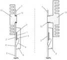
(도6)는 종래기술의 실시 예에 따른 반도체 패캐지 단면도.
(도7)는 " " " " .
(도8)은 " " " " .1 is a cross-sectional view of a semiconductor package according to an embodiment of the present invention.
2 is a cross-sectional view of another semiconductor package according to an embodiment of the present invention.
(Figure 3) is """".
(Figure 4) is """".
(FIG. 5) shows """".
6 is a cross-sectional view of a semiconductor package according to an embodiment of the prior art.
(FIG. 7) is """".
(FIG. 8) shows """".
본 발명은 반도체 패캐지의 일부를 이루고 있는 방열판(heat slug)에 외부 방열판(heat sink/spreader)을 탈/부착할 수 있도록 방열판(heat slug)에 나사(screw) 홈을 형성하여, 이를 패캐지용 방열판으로 사용한다. 즉 (도1)∼(도5)와 같이 ;The present invention forms a screw groove in the heat slug so that a heat sink / spreader can be attached to or detached from a heat slug that forms part of a semiconductor package. Used as That is, as shown in Figs. 1 to 5;
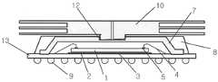
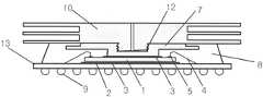
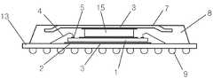
-반도체 칩(chip)(1) -다이 패들(die paddle/pad)(2)Semiconductor chip (1) Die paddle / pad (2)
-접착물질(adhesive material)(3) -미세금선(gold wire)(4)-Adhesive material (3)-gold wire (4)
-본딩 패드(bonding pad)(5) -인너 리드(inner lead)(6)Bonding pads (5) inner lead (6)
-패캐지 방열판(heat slug)(7) -봉지재(epoxy, EMC)(8)-Package heat slug (7)-encapsulant (epoxy, EMC) (8)
-아웃 리드(out lead, I/O)(9) -외부 방열판(heat sink/spreader)(10)-Out lead (I / O) (9) -heat sink / spreader (10)
-세라믹 몸체(ceramic body)(11) -나사(screw)홈(12)-Ceramic body (11) -screw groove (12)
-써브스트레이트(substrate)(13) -금속 뚜껑/덮개(metal lid)(14)-Substrate (13) -metal lid (14)
-열전도성 물질(thermal conductive material)(15)Thermal
등으로 이루어져 있다.Etc.
아울러, 본 발명인 방열판 구조를 사용한 반도체 패캐지 제조 공정의 예로서, (도9a)∼(도9f)와 같이 ;In addition, as an example of a semiconductor package manufacturing process using the heat sink structure of the present invention, as shown in Figs. 9A to 9F;
-반도체 패캐지용 리드프레임(lead frame)의 다이패들(die paddle)(2)에 접착물질(adhesive material)(3)을 사용하여, 반도체 칩(chip)(1)을 부착시킨다. ------ (9a)The
-미세금선(gold wire)(4)을 사용하여, 칩의 본딩패드(bonding pad)(5)와 인너리드(inner lead)(6)를 전기적으로 연결시킨다. ------ (9b)A
-접착물질(adhesive material)(3)을 사용하여, 나사(screw)홈(12)이 형성된 반도체 패캐지용 방열판(heat slug)(7)을 다이패들(die paddle)(2)에 부착시킨다. ------ (9c)An
-몰드 금형(mold die)과 봉지재(epoxy, EMC ; Epoxy Molding ompound)(8)를 사용하여, 칩(1)과 미세금선(4) 및 인너리드(6)의 보호 및 방열판(7)의 일부분이 노출될 수 있도록 봉지(molding)를 실시한다. ------ (9d)Protection of the heat sink (7) and protection of the chip (1), fine gold wire (4) and inner lead (6) using a mold die and an encapsulant (epoxy, EMC; epoxy molding ompound) (8). Molding is performed to expose a portion. ------ (9d)
-반도체 패캐지 방열판(heat slug)(7)이 위로 향할 수 있도록 아웃리드(out lead, I/O)(9)를 형성(trimming & forming)시킨다. ------ (9e)-Trim out & form out lead (I / O) 9 so that the semiconductor
-필요시, 패캐지 방열판(heat slug)(7)에 결합할 수 있게 되어 있는 외부 방열판(heat slug/spreader)(10)을 패캐지 방열판(7)에 결합시킨다. ------ (9f)-If necessary, the heat slug /
Claims (3)
Translated fromKoreanPriority Applications (1)
| Application Number | Priority Date | Filing Date | Title |
|---|---|---|---|
| KR1020120029626AKR20130107670A (en) | 2012-03-23 | 2012-03-23 | Semiconductor package heat slug structure for thermal dissipation and manufacturing this semiconductor package |
Applications Claiming Priority (1)
| Application Number | Priority Date | Filing Date | Title |
|---|---|---|---|
| KR1020120029626AKR20130107670A (en) | 2012-03-23 | 2012-03-23 | Semiconductor package heat slug structure for thermal dissipation and manufacturing this semiconductor package |
Publications (1)
| Publication Number | Publication Date |
|---|---|
| KR20130107670Atrue KR20130107670A (en) | 2013-10-02 |
Family
ID=49630927
Family Applications (1)
| Application Number | Title | Priority Date | Filing Date |
|---|---|---|---|
| KR1020120029626ACeasedKR20130107670A (en) | 2012-03-23 | 2012-03-23 | Semiconductor package heat slug structure for thermal dissipation and manufacturing this semiconductor package |
Country Status (1)
| Country | Link |
|---|---|
| KR (1) | KR20130107670A (en) |
Cited By (2)
| Publication number | Priority date | Publication date | Assignee | Title |
|---|---|---|---|---|
| WO2022073884A1 (en)* | 2020-10-07 | 2022-04-14 | Vitesco Technologies GmbH | Semiconductor assembly and method for producing a semiconductor assembly |
| US12087657B2 (en) | 2021-05-21 | 2024-09-10 | Samsung Electronics Co., Ltd. | Semiconductor packages |
- 2012
- 2012-03-23KRKR1020120029626Apatent/KR20130107670A/ennot_activeCeased
Cited By (2)
| Publication number | Priority date | Publication date | Assignee | Title |
|---|---|---|---|---|
| WO2022073884A1 (en)* | 2020-10-07 | 2022-04-14 | Vitesco Technologies GmbH | Semiconductor assembly and method for producing a semiconductor assembly |
| US12087657B2 (en) | 2021-05-21 | 2024-09-10 | Samsung Electronics Co., Ltd. | Semiconductor packages |
Similar Documents
| Publication | Publication Date | Title |
|---|---|---|
| CN102891123B (en) | stacked die semiconductor package | |
| US9449899B2 (en) | Semiconductor package with heat spreader | |
| US6552428B1 (en) | Semiconductor package having an exposed heat spreader | |
| US8049313B2 (en) | Heat spreader for semiconductor package | |
| CN205376495U (en) | Semiconductor device | |
| CN103378019B (en) | Semiconductor package structure with heat dissipation structure and manufacturing method thereof | |
| KR101388857B1 (en) | Semiconductor package and method of manufacturing the semiconductor package | |
| CN204375722U (en) | A kind of semiconductor package | |
| CN103703549A (en) | Exposed die package for direct surface mounting | |
| US9355945B1 (en) | Semiconductor device with heat-dissipating lead frame | |
| TWI716532B (en) | Resin-encapsulated semiconductor device | |
| US7564123B1 (en) | Semiconductor package with fastened leads | |
| KR20130140354A (en) | Semiconductor package and the method | |
| US20140374891A1 (en) | Semiconductor device with heat spreader and thermal sheet | |
| KR20130107670A (en) | Semiconductor package heat slug structure for thermal dissipation and manufacturing this semiconductor package | |
| TWI237363B (en) | Semiconductor package | |
| CN103441080A (en) | Chip front-mounting BGA encapsulating method | |
| US9165855B1 (en) | Semiconductor device with die attached heat spreader | |
| KR20060036433A (en) | Heat dissipation semiconductor package and manufacture thereof. | |
| US8120169B2 (en) | Thermally enhanced molded leadless package | |
| CN108140630A (en) | IC chip with perpendicular connectors | |
| KR101239117B1 (en) | Power semiconductor package and method for fabricating the same | |
| US20180025965A1 (en) | WFCQFN (Very-Very Thin Flip Chip Quad Flat No Lead) with Embedded Component on Leadframe and Method Therefor | |
| KR100640585B1 (en) | Semiconductor package with improved heat dissipation | |
| KR19990086280A (en) | Semiconductor package |
Legal Events
| Date | Code | Title | Description |
|---|---|---|---|
| A201 | Request for examination | ||
| PA0109 | Patent application | St.27 status event code:A-0-1-A10-A12-nap-PA0109 | |
| PA0201 | Request for examination | St.27 status event code:A-1-2-D10-D11-exm-PA0201 | |
| D13-X000 | Search requested | St.27 status event code:A-1-2-D10-D13-srh-X000 | |
| D14-X000 | Search report completed | St.27 status event code:A-1-2-D10-D14-srh-X000 | |
| E902 | Notification of reason for refusal | ||
| PE0902 | Notice of grounds for rejection | St.27 status event code:A-1-2-D10-D21-exm-PE0902 | |
| E601 | Decision to refuse application | ||
| PE0601 | Decision on rejection of patent | St.27 status event code:N-2-6-B10-B15-exm-PE0601 | |
| PG1501 | Laying open of application | St.27 status event code:A-1-1-Q10-Q12-nap-PG1501 | |
| R18-X000 | Changes to party contact information recorded | St.27 status event code:A-3-3-R10-R18-oth-X000 |