KR20130103908A - Semiconductor device with buried bit line and method for fabricating the same - Google Patents
Semiconductor device with buried bit line and method for fabricating the sameDownload PDFInfo
- Publication number
- KR20130103908A KR20130103908AKR20120024914AKR20120024914AKR20130103908AKR 20130103908 AKR20130103908 AKR 20130103908AKR 20120024914 AKR20120024914 AKR 20120024914AKR 20120024914 AKR20120024914 AKR 20120024914AKR 20130103908 AKR20130103908 AKR 20130103908A
- Authority
- KR
- South Korea
- Prior art keywords
- source
- layer
- trench
- bit line
- buried bit
- Prior art date
- Legal status (The legal status is an assumption and is not a legal conclusion. Google has not performed a legal analysis and makes no representation as to the accuracy of the status listed.)
- Withdrawn
Links
- 239000004065semiconductorSubstances0.000titleclaimsabstractdescription85
- 238000000034methodMethods0.000titleclaimsdescription115
- 239000000758substrateSubstances0.000claimsabstractdescription95
- 238000004519manufacturing processMethods0.000claimsabstractdescription24
- 230000008569processEffects0.000claimsdescription78
- 239000011159matrix materialSubstances0.000claimsdescription18
- 238000005530etchingMethods0.000claimsdescription13
- 230000002265preventionEffects0.000claimsdescription12
- 238000009413insulationMethods0.000abstractdescription3
- 239000010410layerSubstances0.000description362
- 239000012535impuritySubstances0.000description32
- XUIMIQQOPSSXEZ-UHFFFAOYSA-NSiliconChemical compound[Si]XUIMIQQOPSSXEZ-UHFFFAOYSA-N0.000description27
- 229910052710siliconInorganic materials0.000description27
- 239000010703siliconSubstances0.000description27
- 239000002184metalSubstances0.000description25
- 235000012431wafersNutrition0.000description24
- 238000003860storageMethods0.000description22
- 150000004767nitridesChemical class0.000description20
- 229910000577Silicon-germaniumInorganic materials0.000description16
- 230000004888barrier functionEffects0.000description14
- 239000000463materialSubstances0.000description14
- 238000009792diffusion processMethods0.000description12
- 239000013078crystalSubstances0.000description10
- HMDDXIMCDZRSNE-UHFFFAOYSA-N[C].[Si]Chemical compound[C].[Si]HMDDXIMCDZRSNE-UHFFFAOYSA-N0.000description8
- LEVVHYCKPQWKOP-UHFFFAOYSA-N[Si].[Ge]Chemical compound[Si].[Ge]LEVVHYCKPQWKOP-UHFFFAOYSA-N0.000description8
- 239000011229interlayerSubstances0.000description8
- 229910021332silicideInorganic materials0.000description7
- FVBUAEGBCNSCDD-UHFFFAOYSA-Nsilicide(4-)Chemical compound[Si-4]FVBUAEGBCNSCDD-UHFFFAOYSA-N0.000description7
- 230000010354integrationEffects0.000description6
- 230000003647oxidationEffects0.000description6
- 238000007254oxidation reactionMethods0.000description6
- 238000000151depositionMethods0.000description5
- 229910044991metal oxideInorganic materials0.000description5
- 150000004706metal oxidesChemical class0.000description5
- 238000005498polishingMethods0.000description5
- 230000008054signal transmissionEffects0.000description5
- 239000000126substanceSubstances0.000description5
- 230000000295complement effectEffects0.000description4
- 239000002019doping agentSubstances0.000description4
- 229920002120photoresistant polymerPolymers0.000description4
- UFHFLCQGNIYNRP-UHFFFAOYSA-NHydrogenChemical compound[H][H]UFHFLCQGNIYNRP-UHFFFAOYSA-N0.000description2
- 238000005229chemical vapour depositionMethods0.000description2
- 238000004140cleaningMethods0.000description2
- 230000000694effectsEffects0.000description2
- 229910052739hydrogenInorganic materials0.000description2
- 239000001257hydrogenSubstances0.000description2
- 238000005468ion implantationMethods0.000description2
- 238000004381surface treatmentMethods0.000description2
- 230000015572biosynthetic processEffects0.000description1
- 239000003990capacitorSubstances0.000description1
- 238000005520cutting processMethods0.000description1
- 230000006866deteriorationEffects0.000description1
- 230000002542deteriorative effectEffects0.000description1
- 238000010586diagramMethods0.000description1
- 238000002347injectionMethods0.000description1
- 239000007924injectionSubstances0.000description1
- 238000000059patterningMethods0.000description1
- 230000000149penetrating effectEffects0.000description1
- 230000009467reductionEffects0.000description1
- 230000007261regionalizationEffects0.000description1
- 230000004044responseEffects0.000description1
Images


Classifications
- H—ELECTRICITY
- H10—SEMICONDUCTOR DEVICES; ELECTRIC SOLID-STATE DEVICES NOT OTHERWISE PROVIDED FOR
- H10B—ELECTRONIC MEMORY DEVICES
- H10B12/00—Dynamic random access memory [DRAM] devices
- H—ELECTRICITY
- H10—SEMICONDUCTOR DEVICES; ELECTRIC SOLID-STATE DEVICES NOT OTHERWISE PROVIDED FOR
- H10B—ELECTRONIC MEMORY DEVICES
- H10B12/00—Dynamic random access memory [DRAM] devices
- H10B12/01—Manufacture or treatment
- H10B12/02—Manufacture or treatment for one transistor one-capacitor [1T-1C] memory cells
- H10B12/05—Making the transistor
- H10B12/053—Making the transistor the transistor being at least partially in a trench in the substrate
- H—ELECTRICITY
- H10—SEMICONDUCTOR DEVICES; ELECTRIC SOLID-STATE DEVICES NOT OTHERWISE PROVIDED FOR
- H10D—INORGANIC ELECTRIC SEMICONDUCTOR DEVICES
- H10D30/00—Field-effect transistors [FET]
- H10D30/01—Manufacture or treatment
- H10D30/021—Manufacture or treatment of FETs having insulated gates [IGFET]
- H10D30/025—Manufacture or treatment of FETs having insulated gates [IGFET] of vertical IGFETs
- H—ELECTRICITY
- H10—SEMICONDUCTOR DEVICES; ELECTRIC SOLID-STATE DEVICES NOT OTHERWISE PROVIDED FOR
- H10B—ELECTRONIC MEMORY DEVICES
- H10B12/00—Dynamic random access memory [DRAM] devices
- H10B12/30—DRAM devices comprising one-transistor - one-capacitor [1T-1C] memory cells
- H10B12/31—DRAM devices comprising one-transistor - one-capacitor [1T-1C] memory cells having a storage electrode stacked over the transistor
- H10B12/315—DRAM devices comprising one-transistor - one-capacitor [1T-1C] memory cells having a storage electrode stacked over the transistor with the capacitor higher than a bit line
- H—ELECTRICITY
- H10—SEMICONDUCTOR DEVICES; ELECTRIC SOLID-STATE DEVICES NOT OTHERWISE PROVIDED FOR
- H10B—ELECTRONIC MEMORY DEVICES
- H10B12/00—Dynamic random access memory [DRAM] devices
- H10B12/30—DRAM devices comprising one-transistor - one-capacitor [1T-1C] memory cells
- H10B12/48—Data lines or contacts therefor
- H10B12/482—Bit lines
- H—ELECTRICITY
- H10—SEMICONDUCTOR DEVICES; ELECTRIC SOLID-STATE DEVICES NOT OTHERWISE PROVIDED FOR
- H10D—INORGANIC ELECTRIC SEMICONDUCTOR DEVICES
- H10D84/00—Integrated devices formed in or on semiconductor substrates that comprise only semiconducting layers, e.g. on Si wafers or on GaAs-on-Si wafers
- H10D84/01—Manufacture or treatment
- H10D84/0123—Integrating together multiple components covered by H10D12/00 or H10D30/00, e.g. integrating multiple IGBTs
- H10D84/0126—Integrating together multiple components covered by H10D12/00 or H10D30/00, e.g. integrating multiple IGBTs the components including insulated gates, e.g. IGFETs
- H10D84/0165—Integrating together multiple components covered by H10D12/00 or H10D30/00, e.g. integrating multiple IGBTs the components including insulated gates, e.g. IGFETs the components including complementary IGFETs, e.g. CMOS devices
- H—ELECTRICITY
- H10—SEMICONDUCTOR DEVICES; ELECTRIC SOLID-STATE DEVICES NOT OTHERWISE PROVIDED FOR
- H10D—INORGANIC ELECTRIC SEMICONDUCTOR DEVICES
- H10D84/00—Integrated devices formed in or on semiconductor substrates that comprise only semiconducting layers, e.g. on Si wafers or on GaAs-on-Si wafers
- H10D84/01—Manufacture or treatment
- H10D84/02—Manufacture or treatment characterised by using material-based technologies
- H10D84/03—Manufacture or treatment characterised by using material-based technologies using Group IV technology, e.g. silicon technology or silicon-carbide [SiC] technology
- H10D84/038—Manufacture or treatment characterised by using material-based technologies using Group IV technology, e.g. silicon technology or silicon-carbide [SiC] technology using silicon technology, e.g. SiGe
- H—ELECTRICITY
- H10—SEMICONDUCTOR DEVICES; ELECTRIC SOLID-STATE DEVICES NOT OTHERWISE PROVIDED FOR
- H10D—INORGANIC ELECTRIC SEMICONDUCTOR DEVICES
- H10D30/00—Field-effect transistors [FET]
- H10D30/60—Insulated-gate field-effect transistors [IGFET]
- H10D30/67—Thin-film transistors [TFT]
- H10D30/6728—Vertical TFTs
Landscapes
- Engineering & Computer Science (AREA)
- Manufacturing & Machinery (AREA)
- Semiconductor Memories (AREA)
- Thin Film Transistor (AREA)
Abstract
Description
Translated fromKorean본 발명은 반도체 장치 제조 기술에 관한 것으로, 보다 구체적으로는 매립비트라인을 구비한 반도체 장치 및 그 제조방법에 관한 것이다.
The present invention relates to a semiconductor device manufacturing technology, and more particularly to a semiconductor device having a buried bit line and a method of manufacturing the same.
반도체 메모리 장치의 집적도가 증가함에 따라 평면적으로 각 단위셀이 차지하는 면적을 감소시키기 위해 셀 구조가 8F2 및 6F2에서 4F2로 변화되고 있다. 이와 같이, 단위셀의 면적 감소에 대응하여 트랜지스터, 비트라인, 워드라인, 캐패시터 등의 구성요소들을 형성하기 위한 다양한 방법이 제안되었다. 특히, 4F2 셀 구조를 구현하기 위하여 소스 및 드레인을 상하로 배치하여 수직채널을 유도하는 수직 채널 반도체 장치가 제안되었다.As the degree of integration of semiconductor memory devices increases, the cell structure is changed from 8F2 and 6F2 to 4F2 in order to reduce the area occupied by each unit cell in plan. As described above, various methods for forming components such as transistors, bit lines, word lines, and capacitors have been proposed in response to the reduction of the area of the unit cell. In particular, in order to implement a 4F2 cell structure, a vertical channel semiconductor device in which vertical channels are induced by disposing source and drain up and down has been proposed.
수직 채널 반도체 장치는 기판의 주면(main surface)에 대하여 수직으로 연장되는 활성필라(active pillar)의 주위에 게이트전극을 형성하고, 게이트전극을 중심으로 하여 활성필라의 상하에 소스 및 드레인영역을 형성함으로써, 기판의 구면에 대하여 수직으로 채널이 형성된다. 따라서, 반도체 장치의 면적을 감소시키더라도 채널길이에 구애받지 않게 된다.In a vertical channel semiconductor device, a gate electrode is formed around an active pillar extending perpendicular to a main surface of a substrate, and source and drain regions are formed above and below the active pillar around the gate electrode. As a result, a channel is formed perpendicular to the spherical surface of the substrate. Therefore, even if the area of the semiconductor device is reduced, the channel length is not affected.
이와 같이 수직 채널 반도체 장치를 구현하는데 있어서, 비트라인을 활성필라 아래 기판에 매립하는 매립비트라인(Buried Bit Line, BBL) 구조가 제안되었다.As described above, in implementing a vertical channel semiconductor device, a buried bit line (BBL) structure for embedding a bit line in a substrate under an active pillar has been proposed.
종래에는 매립비트라인을 활성필라 사이의 기판에 불순물을 이온주입하여 불순물영역을 형성하고, 활성필라 사이의 기판을 식각하여 불순물영역을 분리시키는 방법으로 매립비트라인을 형성하였으나, 도핑농도의 한계로 인해 매립비트라인의 저항이 크다는 문제점이 있다.Conventionally, the buried bit line is formed by implanting impurities into the substrate between the active pillars to form an impurity region, and etching the substrate between the active pillars to separate the impurity region, but the doping concentration is limited. Therefore, there is a problem that the resistance of the buried bit line is large.
매립비트라인의 저항을 감소시키기 위한 가장 이상적인 방법은 매립비트라인으로 저항이 낮은 금속성막을 사용하는 것이지만, 구조적으로 적용이 쉽지 않다. 일례로, 매립비트라인으로 금속을 사용하기 위하여 활성필라의 일측벽을 노출시키는 콘택(이른바, One Side contact; OSC)을 형성하여 매립비트라인을 형성하는 방법이 제안되었다. 하지만, OSC 구조의 매립비트라인은 그 제조공정이 매우 복잡하고, 고난이도의 제조기술이 요구되기 때문에 양산에 적용하기 어렵다는 문제점이 있다.
The most ideal way to reduce the resistance of the buried bit line is to use a low resistance metallic film as the buried bit line, but it is not easy to apply structurally. For example, in order to use a metal as a buried bit line, a method of forming a buried bit line by forming a contact (so-called One Side contact; OSC) exposing one side wall of an active pillar is proposed. However, the embedded bit line of the OSC structure has a problem that its manufacturing process is very complicated and difficult to apply to mass production because it requires a high level of manufacturing technology.
본 발명의 실시예들은 저저항 매립비트라인을 구비한 반도체 장치 및 그 제조방법을 제공하기 위한 것이다.Embodiments of the present invention provide a semiconductor device having a low resistance buried bit line and a method of manufacturing the same.
본 발명의 실시예에 따른 반도체 장치는 기판에 형성된 트렌치; 상기 트렌치를 일부 매립하는 매립비트라인; 상기 매립비트라인 상의 나머지 상기 트렌치를 매립하는 제1소스/드레인층; 채널층과 제2소스/드레인층이 적층된 구조를 갖고, 상기 채널층이 상기 제1소스/드레인층에 접하도록 상기 제1소스/드레인층에 본딩된 적층패턴; 및 상기 매립비트라인과 교차하고, 상기 채널층의 측벽에 접하는 워드라인을 포함할 수 있다.In an embodiment, a semiconductor device may include a trench formed in a substrate; A buried bit line filling a portion of the trench; A first source / drain layer filling the remaining trench on the buried bit line; A stacked pattern having a structure in which a channel layer and a second source / drain layer are laminated, and bonded to the first source / drain layer such that the channel layer contacts the first source / drain layer; And a word line crossing the buried bit line and in contact with a sidewall of the channel layer.
본 발명의 다른 실시예에 따른 반도체 장치는 기판에 형성된 제1트렌치, 상기 제1트렌치를 일부 매립하는 매립비트라인 및 상기 매립비트라인 상에서 나머지 상기 제1트렌치를 매립하는 제1소스/드레인층을 포함하는 제1구조물; 및 채널층과 제2소스/드레인층이 적층된 적층패턴, 상기 적층패턴 사이를 갭필하는 절연막, 상기 절연막에 형성되어 상기 채널층의 측벽을 노출시키는 제2트렌치 및 상기 제2트렌치에 매립된 워드라인을 포함하는 제2구조물을 포함하고, 상기 매립비트라인과 상기 워드라인이 교차하고, 상기 제1소스/드레인층과 상기 채널층이 접하도록 상기 제1구조물과 상기 제2구조물이 본딩된 것일 수 있다.In an embodiment, a semiconductor device may include a first trench formed in a substrate, a buried bit line filling a portion of the first trench, and a first source / drain layer filling the remaining first trench on the buried bit line. A first structure comprising; And a stacked pattern in which a channel layer and a second source / drain layer are stacked, an insulating film gap gap between the stacked patterns, a second trench formed in the insulating film to expose sidewalls of the channel layer, and a word embedded in the second trench. And a second structure including a line, wherein the buried bit line and the word line intersect with each other, and the first structure and the second structure are bonded to contact the first source / drain layer and the channel layer. Can be.
본 발명의 실시예에 따른 반도체 장치 제조방법은 기판에 트렌치를 형성하는 단계; 상기 트렌치를 일부 매립하는 매립비트라인을 형성하는 단계; 상기 매립비트라인 상에 나머지 상기 트렌치를 매립하는 제1소스/드레인층을 형성하는 단계; 희생기판 전면에 제2소스/드레인층과 채널층을 순차적으로 형성하는 단계; 상기 제1소스/드레인층과 상기 채널층이 서로 마주보도록 상기 기판과 상기 희생기판을 본딩하는 단계; 상기 희생기판을 제거하는 클리빙공정을 실시하는 단계; 상기 제2소스/드레인층 및 상기 채널층을 선택적으로 식각하여 적층패턴을 형성하되, 상기 채널층이 상기 제1소스/드레인층과 접하도록 형성하는 단계; 및 상기 매립비트라인과 교차하고, 상기 채널층 측벽에 접하는 워드라인을 형성하는 단계를 포함할 수 있다.A semiconductor device manufacturing method according to an embodiment of the present invention comprises the steps of forming a trench in a substrate; Forming a buried bit line filling a portion of the trench; Forming a first source / drain layer filling the remaining trench on the buried bit line; Sequentially forming a second source / drain layer and a channel layer on the entire surface of the sacrificial substrate; Bonding the substrate and the sacrificial substrate such that the first source / drain layer and the channel layer face each other; Performing a cleaving process to remove the sacrificial substrate; Selectively etching the second source / drain layer and the channel layer to form a stacked pattern, wherein the channel layer is in contact with the first source / drain layer; And forming a word line crossing the buried bit line and in contact with the sidewall of the channel layer.
본 발명의 다른 실시예에 따른 반도체 장치 제조방법은 기판에 제1트렌치를 형성하는 단계; 상기 제1트렌치를 일부 매립하는 매립비트라인을 형성하는 단계; 상기 매립비트라인 상에 나머지 상기 제1트렌치를 매립하는 제1소스/드레인층을 형성하는 단계; 희생기판 상에 제2소스/드레인층과 채널층이 적층된 적층패턴을 형성하는 단계; 상기 희생기판 상에 상기 적층패턴 사이를 매립하고, 상기 채널층의 측벽을 노출시키는 제2트렌치를 구비한 절연막을 형성하는 단계; 상기 제2트렌치를 매립하는 워드라인을 형성하는 단계; 상기 매립비트라인과 상기 워드라인이 서로 교차하고, 상기 제1소스/드레인층과 상기 채널층이 서로 접하도록 상기 기판과 상기 희생기판을 본딩하는 단계; 및 상기 희생기판을 제거하는 클리빙공정을 실시하는 단계를 포함할 수 있다.
In another embodiment, a method of manufacturing a semiconductor device includes: forming a first trench in a substrate; Forming a buried bit line filling a portion of the first trench; Forming a first source / drain layer filling the remaining first trench on the buried bit line; Forming a stacked pattern in which a second source / drain layer and a channel layer are stacked on the sacrificial substrate; Forming an insulating film on the sacrificial substrate, the insulating layer having a second trench filling the sidewalls of the channel layer and filling the sidewalls of the channel layer; Forming a word line filling the second trench; Bonding the substrate and the sacrificial substrate so that the buried bit line and the word line cross each other and the first source / drain layer and the channel layer contact each other; And performing a cleaving process of removing the sacrificial substrate.
상술한 과제의 해결 수단을 바탕으로 하는 본 기술은 매립비트라인이 형성된 기판에 다른 구조물(예컨대, 채널층, 워드라인 등)을 본딩함으로써, 저저항 매립비트라인을 용이하게 구현할 수 있고, 인접한 매립비트라인 사이의 캐패시턴스를 감소시킬 수 있는 효과가 있다.Based on the above-mentioned means for solving the above problems, the present technology can easily implement a low resistance buried bit line by bonding another structure (eg, a channel layer, a word line, etc.) to a substrate on which buried bit lines are formed. There is an effect that can reduce the capacitance between the bit lines.
또한, 본 기술은 수직 채널 반도체 장치를 구성하는 다수의 구성요소를 분리하여 개별 기판에서 제작한 이후에 본딩함으로써, 구조가 단순하여 집적도를 증가시키기 용이하고, 공정과정을 단순화시킬 수 있으며, 공정난이도를 감소시켜 양산에 적용하기 용이하다는 효과가 있다.
In addition, the present technology separates a plurality of components constituting the vertical channel semiconductor device and fabricates them on individual substrates, and then bonds them to each other, thereby increasing the degree of integration, simplifying the process, and simplifying the process. There is an effect that it is easy to apply to mass production by reducing the.
도 1a 및 도 1b는 본 발명의 제1실시예에 따른 반도체 장치를 도시한 도면
도 2a 내지 도 2i는 본 발명의 제1실시예에 따른 반도체 장치를 제조하기 위한 제조방법의 일례를 도시한 공정단면도.
도 3a 및 도 3b는 본 발명의 제2실시예에 따른 반도체 장치를 도시한 도면.
도 4a 내지 도 4j는 본 발명의 제2실시예에 따른 반도체 장치를 제조하기 위한 제조방법의 일례를 도시한 공정단면도.1A and 1B illustrate a semiconductor device according to a first embodiment of the present invention.
2A to 2I are process cross-sectional views showing one example of a manufacturing method for manufacturing a semiconductor device according to the first embodiment of the present invention.
3A and 3B show a semiconductor device according to a second embodiment of the present invention.
4A to 4J are process cross-sectional views showing one example of a manufacturing method for manufacturing a semiconductor device according to the second embodiment of the present invention.
이하 본 발명이 속하는 기술분야에서 통상의 지식을 가진자가 본 발명의 기술적 사상을 용이하게 실시할 수 있을 정도로 상세히 설명하기 위하여, 본 발명의 가장 바람직한 실시예를 첨부도면을 참조하여 설명하기로 한다.DETAILED DESCRIPTION OF THE PREFERRED EMBODIMENT Hereinafter, preferred embodiments of the present invention will be described in detail with reference to the accompanying drawings, in order to facilitate a person skilled in the art to easily carry out the technical idea of the present invention.
후술할 본 발명의 실시예들은 매립비트라인(Buried Bit Line, BBL)을 구비한 수직 채널 반도체 장치에서 저저항 매립비트라인을 용이하게 구현할 수 있고, 인접한 매립비트라인 사이의 캐패시턴스를 감소시킬 수 있는 반도체 장치를 제공한다. 이를 위해, 본 발명의 실시예들은 수직 채널 반도체 장치를 구성하는 다수의 구성요소를 분리하여(예컨대, 매립비트라인과 워드라인을 분리하여) 개별 기판에서 제작한 이후에 이들을 본딩(Bonding)하여 반도체 장치를 구현하는 것을 기술사상으로 한다.
Embodiments of the present invention to be described later can easily implement a low resistance buried bit line in a vertical channel semiconductor device having a buried bit line (BBL), and can reduce capacitance between adjacent buried bit lines. Provided is a semiconductor device. To this end, embodiments of the present invention are separated by fabricating a plurality of components constituting the vertical channel semiconductor device (for example, by separating the buried bit line and the word line), and then bonding the semiconductors by bonding them. It is a technical idea to implement a device.
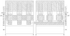
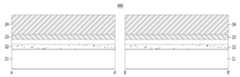
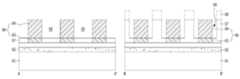
도 1a 내지 도 1b는 본 발명의 제1실시예에 따른 반도체 장치를 도시한 도면이다. 여기서, 도 1a는 평면도, 도 1b는 도 1a에 도시된 A-A'절취선 및 B-B'절취선을 따라 도시한 단면도이다.1A to 1B are diagrams illustrating a semiconductor device in accordance with a first embodiment of the present invention. Here, FIG. 1A is a plan view, and FIG. 1B is a cross-sectional view taken along the line A-A 'and B-B' of FIG. 1A.
도 1a 및 도 1b에 도시된 바와 같이, 본 발명의 제1실시예에 따른 반도체 장치는 기판(101)에 형성된 트렌치(103), 트렌치(103)를 일부 매립하는 매립비트라인(104), 매립비트라인(104) 상에서 나머지 트렌치(103)를 매립하는 제1소스/드레인층(105), 채널층(107)과 제2소스/드레인층(108)이 적층된 구조를 갖고 채널층(107)이 제1소스/드레인층(105)에 접하도록 제1소스/드레인층(105)에 본딩된 적층패턴(109) 및 매립비트라인(104)과 교차하고 채널층(107)의 측벽에 접하는 워드라인(112)을 포함한다.As shown in FIGS. 1A and 1B, the semiconductor device according to the first embodiment of the present inventive concept may include a
트렌치(103)는 매립비트라인(104)과 제1소스/드레인층(105)이 형성될 공간을 제공하기 위한 것으로, B-B'방향으로 연장된 라인타입의 패턴일 수 있다. 이때, 인접한 매립비트라인(104) 사이 및 매립비트라인(104)과 기판(101) 사이를 전기적으로 분리시키기 위하여 트렌치(103)는 기판(101) 상의 제1절연막(102)에 형성될 수 있다. 제1절연막(102)은 산화막, 질화막 및 산화질화막으로 이루어진 그룹으로부터 선택된 어느 하나일 수 있다. 한편, 매립비트라인(104)과 제1소스/드레인층(105)이 매립되는 트렌치(103)는 후술하는 본 발명 제2실시예의 제1트렌치와 같은 형태를 가질 수도 있다.The
트렌치(103)를 일부 매립하는 형태를 갖는 매립비트라인(104)은 신호전달특성을 향상시키기 위하여 저저항물질 예컨대, 금속성막을 포함할 수 있다. 이때, 금속성막은 금속막, 금속산화막, 금속질화막 및 금속실리사이드막을 포함한다.The buried
매립비트라인(104) 상에서 나머지 트렌치(103)를 매립하는 제1소스/드레인층(105)은 불순물이 도핑되고, 단결정상태 또는 다결정상태를 갖는 반도체막을 포함할 수 있다. 이때, 반도체막은 실리콘함유막일 수 있으며, 실리콘함유막은 실리콘막(Si), 실리콘저마늄막(SiGe) 및 실리콘카본막(SiC)으로 이루어진 그룹으로부터 선택된 어느 하나일 수 있다.The first source /
한편, 도면에 도시하지는 않았지만 금속성막을 포함하는 매립비트라인(104)과 반도체막을 포함하는 제1소스/드레인층(105) 사이에는 불순물 확산을 방지하기 위한 도전성 확산방지막 또는 콘택저항을 낮추기 위한 오믹콘택층이 삽입될 수 있다. 물론, 도전성 확산방지막과 오믹콘택층이 적층된 적층막이 삽입될 수도 있다.Although not shown in the drawings, an electrically conductive diffusion barrier layer or ohmic contact for reducing impurity diffusion between the buried
제1소스/드레인층(105)은 적층패턴(109)에 대응하여 매트릭스 배열구조를 가질 수 있다, 즉, 제1소스/드레인층(105)은 A-A'방향 및 B-B'방향으로 각각 제1절연막(102) 및 제2절연막(106)에 분리되어 A-A'방향 및 B-B'방향으로 불연속적으로 배치된 구조를 가질 수 있다. 제2절연막(106)은 매립비트라인(104) 상에서 B-B'방향으로 제1소스/드레인층(105) 사이의 나머지 트렌치(103)를 매립하는 형태를 갖는다. 제2절연막(106)은 산화막, 질화막 및 산화질화막으로 이루어진 그룹으로부터 선택된 어느 하나일 수 있고, 제1절연막(102)과 동일한 물질일 수 있다.The first source /
제1소스/드레인층(105)에 적층패턴(109)이 접하도록 본딩공정을 진행할 때, 본딩특성을 향상시키기 위하여 제1소스/드레인층(105)의 표면은 기판(101)의 표면과 동일면상에 위치할 수 있다. 즉, 본 발명의 제1실시예에서 제1소스/드레인층(105)의 표면은 제1 및 제2절연막(102, 106)의 표면과 동일면상에 위치할 수 있다.When the bonding process is performed such that the
채널층(107)과 제2소스/드레인층(108)이 적층된 구조의 적층패턴(109)은 매립비트라인(104)이 형성되는 기판(101)이 아닌 별도의 희생기판에서 제작되어 채널층(107)이 제1소스/드레인층(105)에 접하도록 본딩된 것이다. 따라서, 적층패턴(109)은 제1소스/드레인층(105)과 완전히 중첩되거나, 또는 적층패턴(109)의 일부만 제1소스/드레인층(105)과 중첩될 수 있다. 즉, 적층패턴(109)의 채널층(107)이 제1소스/드레인층(105)과 완전히 접하거나, 적층패턴(109)의 채널층(107) 일부가 제1소스/드레인층(105)에 접할 수 있다.The
적층패턴(109)은 필라타입(Pillar type)의 패턴으로 매트릭스 배열구조를 가질 수 있고, 제1소스/드레인층(105)은 적층패턴(109)에 대응하는 매트릭스 배열구조일 수 있다. 제1소스/드레인층(105)과 적층패턴(109)은 활성필라(Active Pillar)로 작용한다.The
채널층(107) 및 제2소스/드레인층(108)은 불순물이 도핑되고, 단결정상태 또는 다결정상태를 갖는 반도체막을 포함할 수 있다. 이때, 반도체막은 실리콘함유막일 수 있으며, 실리콘함유막은 실리콘막(Si), 실리콘저마늄막(SiGe) 및 실리콘카본막(SiC)으로 이루어진 그룹으로부터 선택된 어느 하나일 수 있다.The
여기서, 제1소스/드레인층(105) 및 제2소스/드레인층(108)은 결정상태에 따른 영향이 반도체 장치의 동작특성이 크게 영향을 미치지 않으나, 채널층(107)은 실질적인 전하의 이동경로이기에 다결정상태보다는 단결정상태를 갖는 것이 바람직하다. 반도체 장치의 동작특성을 제어하기 위해 제1소스/드레인층(105), 채널층(107) 및 제2소스/드레인층(108)은 모두 동일한 반도체막이거나, 또는 모두 상이한 반도체막일 수 있다. 또한, 제1소스/드레인층(105)과 제2소스/드레인층(108)은 서로 동일한 반도체막일 수 있고, 채널층(107)은 제1소스/드레인층(105) 및 제2소스/드레인층(108)과는 상이한 반도체막일 수 있다. 그리고, 제1소스/드레인층(105)과 제2소스/드레인층(108)은 서로 동일한 도전형일 수 있고, 채널층(107)은 제1소스/드레인층(105) 및 제2소스/드레인층(108)과 서로 상보적인 도전형일 수 있다. 일례로, 제1소스/드레인층(105) 및 제2소스/드레인층(108)의 도전형은 N형일 수 있고, 채널층(107)의 도전형은 P형일 수 있다.Here, in the first source /
워드라인(112)은 매립비트라인(104)과 교차하는 방향(즉, A-A'방향)으로 연장된 라인타입의 패턴으로, A-A'방향으로 배치된 채널층(107)의 측벽에 접하는 형태를 갖는다. 이때, 워드라인(112)은 도면에 도시된 것처럼 채널층(107)을 감싸는 형태를 가지거나, 채널층(107)의 측벽 일부에 접하는 형태, 또는 채널층(107)의 일측벽에 접하는 제1도전라인과 타측벽에 접하는 제2도전라인으로 구성된 형태(즉, 워드라인 = 제1도전라인+제2도전라인)를 가질 수 있다.The
워드라인(112)은 신호전달특성을 향상시키기 위하여 금속성막을 포함할 수 있다. 그리고, 워드라인(112)과 채널층(107) 사이에는 게이트절연막(111)이 삽입되어 있으며, 게이트절연막(111)은 워드라인(112)의 하부면까지 확장된 형태를 가질 수 있다. 구체적으로, 게이트절연막(111)은 적층패턴(109)을 포함한 구조물 표면을 따라 형성된 형태를 가질 수 있으며, 채널층(107)과 워드라인(112) 사이와 더불어서 제1절연막(102) 및 제2절연막(106)과 워드라인(112) 사이에도 삽입된 형태를 가질 수 있다. 이는, 적층패턴(109) 형성공정시 오정렬에 의해 제1소스/드레인층(105)이 노출되더라도 제1소스/드레인층(105)이 워드라인(112)과 쇼트되는 것을 방지하기 위함이다.The
또한, 본 발명의 제1실시예에 따른 반도체 장치는 적층패턴(109) 상의 하드마스크패턴(110), 하드마스크패턴(110)을 포함한 적층패턴(109) 사이를 갭필하는 제3절연막(113), 하드마스크패턴(110) 상에 형성된 스토리지노드(115), 하드마스크를(110) 관통하여 스토리지노드(115)와 제2소스/드레인층(108)을 연결하는 스토리지노드콘택플러그(114), 스토리지노드(115)를 포함한 구조물 표면을 따라 형성된 유전막(116) 및 유전막(116) 상의 플레이트 전극(117)을 더 포함할 수 있다.In addition, in the semiconductor device according to the first embodiment of the present invention, the third insulating
하드마스크패턴(110)은 워드라인(112)과 스토리지노드(115) 사이의 간섭을 방지하기 위한 간격을 제공함과 동시에 적층패턴(109) 형성공정시 식각장벽으로 작용하고, 제3절연막(113)은 적층패턴(109) 사이 및 워드라인(112) 사이를 전기적으로 분리시키는 역할을 수행한다. 하드마스크패턴(110) 및 제3절연막(113)은 산화막, 질화막 및 산화질화막으로 이루어진 그룹으로부터 선택된 어느 하나일 수 있다.The
상술한 구조를 갖는 본 발명의 제1실시예에 따른 반도체 장치는 매립비트라인(104)을 금속성막으로 형성함으로서 저저항 매립비트라인(104)을 구현할 수 있고, 매립비트라인(104)이 형성된 기판(101)에 적층패턴(109)을 본딩함으로서 저저항 매립비트라인(104)을 손쉽게 형성할 수 있다.In the semiconductor device according to the first embodiment of the present invention having the above-described structure, the buried
또한, 매립비트라인(104)과 적층패턴(109)를 본딩하여 수직 채널 반도체 장치를 구현함으로서, 각각의 구조가 단순하여 집적도를 용이하게 향상시킬 수 있고, 인접한 매립비트라인(104) 사이의 캐패시턴스를 감소시킬 수 있다.In addition, by implementing the vertical channel semiconductor device by bonding the buried
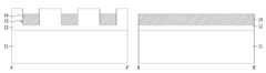
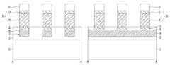
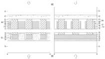
도 2a 내지 도 2i는 본 발명의 제1실시예에 따른 반도체 장치를 제조하기 위한 제조방법의 일례를 도시한 공정단면도이다. 여기서, 도 2a 내지 도 2i는 도 1a에 도시된 A-A'절취선 및 B-B'절취선을 따라 도시한 것이다.2A to 2I are process cross-sectional views showing an example of a manufacturing method for manufacturing a semiconductor device according to the first embodiment of the present invention. 2A to 2I are views taken along the line AA ′ cutting line and line BB ′ shown in FIG. 1A.
도 2a에 도시된 바와 같이, 기판(11)상에 제1절연막(12)을 형성한다. 제1절연막(12)은 산화막, 질화막 및 산화질화막으로 이루어진 그룹으로부터 선택된 어느 하나로 형성할 수 있다.As shown in FIG. 2A, a first insulating
다음으로, 제1절연막(12) 상에 감광막패턴(미도시)을 형성한 이후에 감광막패턴을 식각장벽(etch barrier)으로 제1절연막(12)을 식각하여 다수의 트렌치(13)를 형성한다. 이때, 트렌치(13)는 매립비트라인과 제1소스/드레인층이 형성될 공간을 제공하기 위한 것이다. 따라서, 트렌치(13)가 형성된 제1절연막(12)은 인접한 매립비트라인 사이 및 매립비트라인과 기판(11) 사이를 전기적으로 분리시키는 역할을 수행한다. 트렌치(13)는 일방향 예컨대, 매립비트라인이 연장되는 B-B'방향으로 연장된 라인타입의 패턴으로 형성할 수 있다.Next, after the photoresist pattern (not shown) is formed on the
도 2b에 도시된 바와 같이, 트렌치(13)를 일부 매립하는 매립비트라인(14)을 형성한다. 이때, 매립비트라인(14)이 트렌치(13)를 일부만 매립하도록 형성하는 것은 후속에서 제1소스/드레인층이 형성될 공간을 제공하기 위함이다.As shown in FIG. 2B, a buried
매립비트라인(14)은 신호전달특성을 향상시키기 위하여 금속성막으로 형성한다. 구체적으로, 매립비트라인(14)은 금속막, 금속질화막, 금속산화막 및 금속실리사이드막으로 이루어진 그룹으로부터 선택된 어느 하나 또는 둘 이상이 적층된 적층막으로 형성할 수 있다.The buried
트렌치(13)를 일부 매립하는 매립비트라인(14)는 트렌치(13)를 매립하도록 기판(11) 전면에 금속성막을 증착한 이후에 금속성막에 대한 전면식각 예컨대, 에치백(etchback)을 실시하는 일련의 공정과정을 통해 형성할 수 있다. 일례로, 매립비트라인(14)을 금속실리사이드막으로 형성하는 경우에는 트렌치(13) 내부에 트렌치(13)를 일부 매립하는 실리콘막을 형성하고, 실리콘막을 포함한 기판(11) 전면에 금속막을 형성한 후에 실리콘막이 금속막과 모두 반응하여 금속실리사이드막이 될 때까지 열처리를 실시한 다음, 잔류하는 금속막을 제거하는 일련의 공정과정을 진행할 수 있다.The buried
도 2c에 도시된 바와 같이, 매립비트라인(14) 상에 나머지 트렌치(13)를 매립하는 제1소스/드레인층(15)을 형성한다. 제1소스/드레인층(15)은 불순물이 도핑되고, 다결정상태 또는 단결정상태를 갖는 반도체막으로 형성할 수 있다. 이때, 반도체막은 실리콘함유막일 수 있으며, 실리콘함유막은 실리콘막(Si), 실리콘저마늄막(SiGe) 및 실리콘카본막(SiC)으로 이루어진 그룹으로부터 선택된 어느 하나일 수 있다. 제1소스/드레인층(15)은 후속 공정을 통해 형성될 트랜지스터에서 접합영역으로 작용하기 때문에 제1소스/드레인층(15)을 형성함과 동시에 제1소스/드레인층(15)에 불순물을 도핑시키거나, 또는 제1소스/드레인층(15)을 형성한 이후에 불순물을 도핑시킬 수 있다. 일례로, 제1소스/드레인층(15)은 N형 불순물을 도핑시킬 수 있다.As shown in FIG. 2C, a first source /
트렌치(13)를 매립하는 제1소스/드레인층(15)은 기판(11) 전면에 반도체막을 형성한 이후에 제1절연막(12)이 노출될때까지 평탄화공정을 실시하는 일련의 공정과정을 통해 형성할 수 있다. 이때, 평탄화공정은 화학적기계적연마법(CMP)으로 사용하여 실시할 수 있다.The first source /
한편, 제1소스/드레인층(15)을 형성하기 이전에 매립비트라인(14)과 제1소스/드레인층(15) 사이의 확산을 방지하는 도전성 확산방지막(미도시)을 형성하거나, 매립비트라인(14)과 제1소스/드레인층(15) 사이의 콘택저항을 감소시키기 위한 오믹콘택층(미도시) 형성할 수도 있다. 물론, 도전성 확산방지막과 오믹콘택층이 적층된 적층막을 매립비트라인(14)과 제1소스/드레인층(15) 사이에 형성할 수도 있다.Meanwhile, before forming the first source /
다음으로, 후속 공정을 통해 형성될 적층패턴에 대응하도록 제1소스/드레인층(15)을 선택적으로 식각한다. 적층패턴에 대응하도록 식각된 제1소스/드레인층(15)은 매립비트라인(14) 상에서 매트릭스 형태로 배치된 구조를 갖는다. 즉, 제1소스/드레인층(15)을 적층패턴에 대응하도록 식각한 이후에는 매립비트라인(14)이 연장된 방향으로 제1소스/드레인층(15)이 불연속적으로 배치된 형태를 갖는다.Next, the first source /
다음으로, 매립비트라인(14) 상에 식각된 제1소스/드레인층(15) 사이를 매립하는 제2절연막(16)을 형성한다. 제2절연막(16)은 인접한 제1소스/드레인층(15) 사이를 전기적으로 분리시킴과 동시에 후속 공정간 매립비트라인(14)을 보호하는 역할을 수행한다. 또한, 후속 공정을 통해 형성될 워드라인과 매립비트라인(14) 사이를 전기적으로 분리시키는 역할도 수행한다. 제2절연막(16)은 산화막, 질화막 및 산화질화막으로 이루어진 그룹으로부터 선택된 어느 하나로 형성할 수 있으며, 제1절연막(12)과 동일한 물질로 형성할 수 있다.Next, a second insulating
이하, 설명의 편의를 위하여 기판(11) 상에 제1절연막(12), 트렌치(13), 매립비트라인(14), 제1소스/드레인층(15) 및 제2절연막(16)을 포함하는 제1구조물을 '제1웨이퍼(300)'이라 표기하기로 한다.Hereinafter, for convenience of description, a first insulating
도 2d에 도시된 바와 같이, 스플리팅층(22)이 형성된 희생기판(21) 상에 제2소스/드레인층(23)과 채널층(24)을 순차적으로 형성한다. 스플리팅층(22)은 후속 클리빙공정(cleaving process)시 본딩된 두 웨이퍼를 분리시키기 위한 것으로, 희생기판(21)에 기화성 물질(예컨대, 수소)을 이온주입하여 형성할 수 있다. 참고로, 스플리팅층(22)은 제2소스/드레인층(23)과 채널층(24)을 형성하기 이전에 형성하거나, 또는 이들을 형성한 이후에 형성할 수 있다.As shown in FIG. 2D, the second source /
제2소스/드레인층(23) 및 채널층(24)은 불순물이 도핑되고, 다결정상태 또는 단결정상태를 갖는 반도체막으로 형성할 수 있다. 이때, 반도체막은 실리콘함유막일 수 있으며, 실리콘함유막은 실리콘막(Si), 실리콘저마늄막(SiGe) 및 실리콘카본막(SiC)으로 이루어진 그룹으로부터 선택된 어느 하나로 형성할 수 있다.The second source /
여기서, 트랜지스터의 동작특성을 제어하기 위하여 채널층(24), 제1 및 제2소스/드레인층(15, 23)은 모두 동일한 반도체 물질로 형성하거나, 또는 모두 상이한 반도체 물질로 형성할 수도 있다. 또한, 제1 및 제2소스/드레인층(15, 23)은 서로 동일한 반도체 물질로 형성하고, 채널층(24)은 제1 및 제2소스/드레인층(15, 23)과는 상이한 반도체 물질로 형성할 수 있다. 그리고, 채널층(24)은 후속 공정을 통해 형성될 트랜지스터에서 채널영역으로 작용하고, 제2소스/드레인층(23)은 트랜지스터의 접합영역으로 작용하기 때문에 제2소스/드레인층(23) 및 채널층(24)은 이들은 형성함과 동시에 불순물을 도핑시키거나, 또는 이들을 형성한 이후에 불순물을 도핑시킬 수 있다. 제1 및 제2소스/드레인층(15, 23)은 서로 동일한 도전형을 갖도록 불순물을 도핑시킬 수 있고, 채널층(24)은 제1 및 제2소스/드레인층(15, 23)과 서로 상보적인 도전형을 갖도록 도핑시킬 수 있다. 일례로, 제1 및 제2소스/드레인층(15, 23)에는 N형 불순물을 도핑시킬 수 있고, 채널층(24)에는 P형 불순물을 도핑시킬 수 있다.In this case, the
이하, 설명의 편의를 위하여 스플리팅층(22)이 형성된 희생기판(21)상에 채널층(24) 및 제2소스/드레인층(23)을 포함하는 제2구조물을 '제2웨이퍼(400)'라 표기하기로 한다.Hereinafter, for convenience of description, the second structure including the
도 2e에 도시된 바와 같이, 제1웨이퍼(300)에서 제1절연막(12), 제1소스/드레인층(15) 및 제2절연막(16)이 노출되는 표면과 제2웨이퍼(400)에서 채널층(24)의 표면이 서로 마주보도록 정렬시킨 이후에 제1웨이퍼(300)와 제2웨이퍼(400)를 본딩(bonding)한다. 이때, 웨이퍼 본딩은 공지된 다양한 기술을 사용하여 실시할 수 있으며, 제1 및 제2웨이퍼(300, 400)를 본딩하기 이전에 이들 사이의 접착력을 향상시키기 위하여 소정의 표면처리를 실시할 수 있다.As shown in FIG. 2E, the surface of the
한편, 제1웨이퍼(300)에는 매립비트라인(14)을 형성하고, 제2웨이퍼(400)에 채널층(24), 제1 및 제2소스/드레인층(15, 23)이 적층된 적층막을 형성한 이후에 이들을 본딩하여 상기와 같은 구조물을 형성할 수도 있다. 하지만, 이 경우에는 후속 적층패턴을 형성하기 위한 식각공정시 오정렬에 의하여 적층패턴 아래 매립비트라인(14)이 노출되어 반도체 장치의 특성이 열화될 수 있다. 그러나, 본 발명의 실시예와 같이 매립비트라인(14) 상에 제1소스/드레인층(15)을 형성한 상태에서 제1 및 제2웨이퍼(300, 400)를 본딩하고 후속 적층패턴 형성을 위한 식각공정을 진행하면 오정렬이 발생하더라도 매립비트라인(14)이 노출되는 것을 방지할 수 있으며, 적층패턴을 형성하기 위한 식각공정시 공정마진을 증가시킬 수 있는 장점이 있다.Meanwhile, a buried
도 2f에 도시된 바와 같이, 스플리팅층(22)에 물리적 충격을 인가하여 희생기판(21)을 제거하는 클리빙공정을 실시한다. 이때, 클리빙공정은 공지된 다양한 기술을 사용하여 실시할 수 있다.As illustrated in FIG. 2F, a cleaving process of removing the
다음으로, 클리빙공정 이후에 잔류하는 잔류물을 제거한다. 예컨대, 제2소스/드레인층(23)의 표면이 노출될때까지 평탄화공정을 실시하여 클리빙공정 이후에 잔류하는 스플리팅층(22) 및 희생기판(21)을 제거하고, 연속해서 세정공정을 실시할 수 있다.Next, residues remaining after the cleaving process are removed. For example, the planarization process is performed until the surface of the second source /
도 2g에 도시된 바와 같이, 제2소스/드레인층(23) 상에 하드마스크패턴(31)을 형성한 이후에 하드마스크패턴(31)을 식각장벽으로 제2소스/드레인층(23) 및 채널층(24)을 식각하여 적층패턴(30)을 형성한다. 식각공정이 완료된 시점에서 제1소스/드레인층(15), 채널층(24), 제2소스/드레인층(23) 및 하드마스크패턴(31)이 순차적으로 적층된 형태를 갖는다.As shown in FIG. 2G, after the
적층패턴(30)은 필라타입의 패턴으로 형성할 수 있고, A-A'방향 및 B-B'방향으로 각각 소정간격 이격된 매트릭스 배열구조를 갖도록 형성할 수 있다. 그리고, 적층패턴(30)은 채널층(24)이 제1소스/드레인층(15)과 완전히 접하거나, 또는 채널층(24)이 제1소스/드레인층(15) 일부와 접하도록 형성할 수 있다.The
도 2h에 도시된 바와 같이, 적층패턴(30)을 포함한 구조물 표면을 따라 게이트절연막(32)을 형성한다. 이때, 적층패턴(30)를 포함한 구조물 표면을 따라 게이트절연막(32)을 형성하는 것은 공정간 제2절연막(16)의 손실에 따른 매립비트라인(14)과 후속 공정을 통해 형성될 워드라인 사이의 쇼트를 방지하기 위함이다. 또한, 적층패턴(30)을 형성하는 과정에서 오정렬이 발생할 경우에 노출되는 제1소스/드레인층(15)과 워드라인 사이의 쇼트를 방지하기 위함이다.As shown in FIG. 2H, the
게이트절연막(32)은 산화법(예컨대, 열산화법) 또는 증착법(예컨대, 화학기상증착법)을 사용하여 형성할 수 있다. 또한, 게이트절연막(32)은 산화법을 사용하여 채널층(24) 및 제2소스/드레인층(23)의 측벽에 일정 두께를 형성한 이후에 나머지 두께는 증착법을 사용하여 형성할 수도 있다.The
다음으로, 제1절연막(12) 및 제2절연막(16) 상에 매립비트라인(14)과 교차하는 방향(즉, A-A'방향)으로 연장되고, 적층패턴(30)에 접하는 워드라인(33)을 형성한다. 이때, 워드라인(33)은 적층패턴(30)에서 채널층(24)의 측벽에 접합도록 형성한다. 워드라인(33)은 금속성막으로 형성할 수 있다. 워드라인(33)은 적층패턴(30)의 일측면에 접하는 형태, 적층패턴(30)의 일측면에 접하는 제1도전라인과 타측면에 접하는 제2도전라인으로 이루어진 형태, 또는 적층패턴(30)을 감싸는 형태를 갖도록 형성할 수 있다. 워드라인(33)과 적층패턴(30) 사이에는 게이트절연막(32)이 위치하기 때문에 워드라인(33)은 게이트전극으로도 작용한다.Next, word lines extending on the first insulating
워드라인(33)은 기판(11) 전면에 도전막을 증착한 이후에 리세스공정을 실시하여 도전막의 높이를 조절한 다음, 매립비트라인(14)과 교차하는 방향으로 연장된 라인타입의 패턴으로 도전막을 패터닝하는 일련의 공정과정을 통해 형성할 수 있다.After the conductive film is deposited on the entire surface of the
도 2i에 도시된 바와 같이, 워드라인(33)을 포함한 구조물 전면을 덮도록 제3절연막(34)을 형성한 이후에 하드마스크패턴(31)이 노출될때까지 평탄화공정을 실시한다. 이때, 제3절연막(34)은 산화막, 질화막 및 산화질화막으로 이루어진 그룹으로부터 선택된 어느 하나로 형성할 수 있고, 평탄화공정은 화학적기계적연마법을 사용하여 실시할 수 있다.As shown in FIG. 2I, after the third insulating
참고로, 제2소스/드레인층(23)이 노출될때까지 평탄화공정을 실시할 수도 있으나, 이 경우에는 후속 공정을 통해 형성될 스토리지노드(36)와 워드라인(33) 사이의 충분한 간격이 확보되지 않아 스토리지노드(36) 형성공정에 대한 마진이 감소하거나, 이들 사이의 간섭에 의하여 동작특성이 열화될 우려가 있다.For reference, the planarization process may be performed until the second source /
다음으로, 하드마스크패턴(31)을 관통하여 제2소스/드레인층(23)에 연결되는 스토리지노드콘택플러그(35) 형성공정, 스토리지노드(36) 형성공정, 유전막(37) 형성공정 및 플레이트 전극(38) 형성공정을 순차적으로 실시하여 매립비트라인(14)을 구비한 수직 채널 반도체 장치를 완성한다.Next, a process of forming a storage
상술한 본 발명의 실시예에 따른 반도체 장치 제조방법에 따르면, 매립비트라인(14)을 금속성막으로 형성함으로서 저저항 매립비트라인(14)을 구현할 수 있고, 매립비트라인(14)이 형성된 기판(11)에 적층패턴(30)을 본딩함으로서 저저항 매립비트라인(14)을 손쉽게 형성할 수 있다.According to the semiconductor device manufacturing method according to the embodiment of the present invention described above, by forming the buried
또한, 매립비트라인(14)과 적층패턴(30)를 본딩하여 수직 채널 반도체 장치를 구현함으로서, 각각의 구조가 단순하여 집적도를 용이하게 향상시킬 수 있고, 공정과정을 단순화시킬 수 있으며, 공정난이도를 감소시켜 양산에 적용하기 용이하다. 아울러, 인접한 매립비트라인(14) 사이의 캐패시턴스를 감소시킬 수도 있다.
In addition, by implementing the vertical channel semiconductor device by bonding the buried
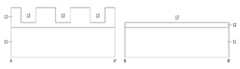
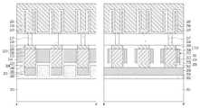
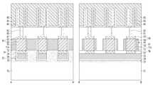
도 3a 내지 도 3b는 본 발명의 제2실시예에 따른 반도체 장치를 도시한 도면이다. 여기서, 도 3a는 평면도이고, 도 3b는 도 3a에 도시된 A-A'절취선 및 B-B'절취선을 따라 도시한 단면도이다.3A to 3B illustrate a semiconductor device according to a second embodiment of the present invention. 3A is a plan view, and FIG. 3B is a cross-sectional view taken along the line AA ′ and BB ′ shown in FIG. 3A.
도 3a 및 도 3b에 도시된 바와 같이, 본 발명의 제2실시예에 따른 반도체 장치는 기판(201)에 형성된 제1트렌치(203), 제1트렌치(203)를 일부 매립하는 매립비트라인(205) 및 매립비트라인(205) 상에서 나머지 제1트렌치(203)를 매립하는 제1소스/드레인층(206)을 포함하는 제1구조물을 포함한다. 또한, 채널층(208)과 제2소스/드레인층(209)이 적층된 적층패턴(210), 적층패턴(210) 사이를 갭필하는 제3절연막(211), 제3절연막(211)에 형성되어 채널층(208)의 측벽을 노출시키는 제2트렌치(212) 및 제2트렌치(212)에 매립된 워드라인(214)을 포함하는 제2구조물을 포함한다. 이때, 본 발명의 제2실시예에 따른 반도체 장치는 매립비트라인(205)과 워드라인(214)이 교차하고, 제1소스/드레인층(206)과 채널층(208)이 서로 접하도록 제1구조물과 제2구조물이 본딩된 것이 특징이다.As shown in FIGS. 3A and 3B, the semiconductor device according to the second exemplary embodiment may include a buried bit line filling a portion of the
제1트렌치(203)는 매립비트라인(205)과 제1소스/드레인층(206)이 형성될 공간을 제공하기 위한 것으로, B-B'방향으로 연장된 라인타입의 패턴일 수 있다. 이때, 인접한 매립비트라인(205) 및 매립비트라인(205)과 기판(201) 사이의 펀치쓰루를 방지하기 위하여 제1트렌치(203)는 기판(201)에 형성된 펀치쓰루방지층(202) 내에 형성될 수 있다. 펀치쓰루방지층(202)은 기판(201)에 불순물을 이온주입하여 형성된 불순물층일 수 있다. 그리고, 인접한 매립비트라인(205) 사이 및 매립비트라인(205)과 기판(201) 사이를 전기적으로 분리시키기 위하여 제1트렌치(203)를 포함한 기판(201) 표면에는 제1절연막(204)이 형성될 수 있다. 제1절연막(204)은 산화막, 질화막 및 산화질화막으로 이루어진 그룹으로부터 선택된 어느 하나일 수 있다. 한편, 매립비트라인(205)과 제1소스/드레인층(206)이 매립되는 제1트렌치(203)는 전술한 본 발명의 제1실시예의 트렌치와 같은 형태를 가질 수 있다.The
제1트렌치(203)를 일부 매립하는 형태를 갖는 매립비트라인(205)은 신호전달특성을 향상시키기 위하여 저저항물질 예컨대, 금속성막을 포함할 수 있다. 이때, 금속성막은 금속막, 금속산화막, 금속질화막 및 금속실리사이드막을 포함한다.The buried
매립비트라인(205) 상에서 나머지 제1트렌치(203)를 매립하는 제1소스/드레인층(206)은 불순물이 도핑되고, 단결정상태 또는 다결정상태를 갖는 반도체막을 포함할 수 있다. 이때, 반도체막은 실리콘함유막일 수 있으며, 실리콘함유막은 실리콘막(Si), 실리콘저마늄막(SiGe) 및 실리콘카본막(SiC)으로 이루어진 그룹으로부터 선택된 어느 하나일 수 있다.The first source /
한편, 도면에 도시하지는 않았지만 금속성막을 포함하는 매립비트라인(205)과 반도체막을 포함하는 제1소스/드레인층(206) 사이에는 불순물 확산을 방지하기 위한 도전성 확산방지막 또는 콘택저항을 낮추기 위한 오믹콘택층이 삽입될 수 있다. 물론, 도전성 확산방지막과 오믹콘택층이 적층된 적층막이 삽입될 수도 있다.Although not shown in the drawings, an electrically conductive diffusion barrier layer or ohmic contact for reducing impurity diffusion between the buried
제1소스/드레인층(206)은 적층패턴(210)에 대응하여 매트릭스 배열구조를 가질 수 있다, 즉, 제1소스/드레인층(206)은 A-A'방향으로는 제1절연막(204)에 의해 분리되고, B-B'방향으로는 제2절연막(207)에 의하여 분리된 구조를 가질 수 있다. 제2절연막(207)은 매립비트라인(205) 상에서 제1소스/드레인층(206) 사이의 나머지 제1트렌치(203)를 매립하는 형태를 갖는다. 제2절연막(207)은 산화막, 질화막 및 산화질화막으로 이루어진 그룹으로부터 선택된 어느 하나일 수 있고, 제1절연막(204)과 동일한 물질일 수 있다.The first source /
제1소스/드레인층(206)에 적층패턴(210)이 접하도록 본딩공정을 진행할 때, 본딩특성을 향상시키기 위하여 제1소스/드레인층(206)의 표면은 기판(201)의 표면과 동일면상에 위치할 수 있다. 즉, 본 발명의 제2실시예에서 제1소스/드레인층(206)의 표면은 제1 및 제2절연막(207)의 표면과 동일면상에 위치할 수 있다.When the bonding process is performed such that the
채널층(208)과 제2소스/드레인층(209)이 적층된 구조의 적층패턴(210)은 매립비트라인(205)이 형성되는 기판(201)이 아닌 희생기판(201)에서 제작되어 채널층(208)이 제1소스/드레인층(206)에 접하도록 본딩된 것이다. 따라서, 적층패턴(210)은 제1소스/드레인층(206)과 완전히 중첩되거나, 또는 적층패턴(210)의 일부만 제1소스/드레인층(206)과 중첩될 수 있다. 즉, 적층패턴(210)의 채널층(208)이 제1소스/드레인층(206)과 완전히 접하거나, 적층패턴(210)의 채널층(208) 일부가 제1소스/드레인층(206)에 접할 수 있다.The
적층패턴(210)은 필라타입의 패턴으로 매트릭스 배열구조를 가질 수 있고, 제1소스/드레인층(206)은 적층패턴(210)에 대응하는 매트릭스 배열구조일 수 있다. 그리고, 제1소스/드레인층(206)과 적층패턴(210)은 활성필라로 작용한다.The
채널층(208) 및 제2소스/드레인층(209)은 불순물이 도핑되고, 단결정상태 또는 다결정상태를 갖는 반도체막을 포함할 수 있다. 이때, 반도체막은 실리콘함유막일 수 있으며, 실리콘함유막은 실리콘막(Si), 실리콘저마늄막(SiGe) 및 실리콘카본막(SiC)으로 이루어진 그룹으로부터 선택된 어느 하나일 수 있다.The
여기서, 반도체 장치의 동작특성을 제어하기 위해 제1소스/드레인층(206), 채널층(208) 및 제2소스/드레인층(209)은 모두 동일한 반도체막이거나, 또는 모두 상이한 반도체막일 수 있다. 또한, 제1소스/드레인층(206)과 제2소스/드레인층(209)은 서로 동일한 반도체막일 수 있고, 채널층(208)은 제1소스/드레인층(206) 및 제2소스/드레인층(209)과는 상이한 반도체막일 수 있다. 그리고, 제1소스/드레인층(206)과 제2소스/드레인층(209)은 서로 동일한 도전형일 수 있고, 채널층(208)은 제1소스/드레인층(206) 및 제2소스/드레인층(209)과 서로 상보적인 도전형일 수 있다. 일례로, 제1소스/드레인층(206) 및 제2소스/드레인층(209)의 도전형은 N형일 수 있고, 채널층(208)의 도전형은 P형일 수 있다.Here, the first source /
워드라인(214)은 적층패턴(210) 사이를 갭필하는 제3절연막(211)에 형성된 제2트렌치(212)에 매립된 형태를 가질 수 있으며, 워드라인(214)과 제2트렌치(212)가 형성된 제3절연막(211)은 적층패턴(210)과 같이 희생기판(201)에 제작되어 기판(201)에 본딩된 것이다. 워드라인(214)은 매립비트라인(205)과 교차하는 방향(즉, A-A'방향)으로 연장된 라인타입의 패턴으로, A-A'방향으로 배치된 채널층(208)의 측벽에 접하는 형태를 갖는다. 이때, 워드라인(214)은 도면에 도시된 것처럼 채널층(208)을 감싸는 형태를 가지거나, 채널층(208)의 측벽 일부에 접하는 형태, 또는 채널층(208)의 일측벽에 접하는 제1도전라인과 타측벽에 접하는 제2도전라인으로 구성된 형태(즉, 워드라인(214) = 제1도전라인+제2도전라인)를 가질 수 있다. 제3절연막(211)은 산화막, 질화막 및 산화질화막으로 이루어진 그룹으로부터 선택된 어느 하나일 수 있다.The
워드라인(214)은 제2트렌치(212)에 일부 매립된 형태를 가질 수 있고, 워드라인(214) 상에서 나머지 제2트렌치(212)를 제4절연막(215)이 매립될 수 있다. 제4절연막(215)은 워드라인(214)과 제1소스/드레인층(206) 사이의 쇼트를 방지하는 역할을 수행하는 것으로 산화막, 질화막 및 산화질화막으로 이루어진 그룹으로부터 선택된 어느 하나일 수 있다.The
워드라인(214)은 신호전달특성을 향상시키기 위해 금속성막을 포함할 수 있고, 워드라인(214)과 채널층(208) 사이에는 게이트절연막(213)이 삽입되어 있다.The
또한, 본 발명의 제2실시예에 따른 반도체 장치는 적층패턴(210) 상의 층간절연막(216), 층간절연막(216) 상의 스토리지노드(218), 층간절연막(216)을 관통하여 스토리지노드(218)와 제2소스/드레인층(209)을 연결하는 스토리지노드콘택플러그(217), 스토리지노드(218)를 포함한 구조물 표면을 따라 형성된 유전막(219) 및 유전막(219) 상의 플레이트 전극(220)을 더 포함할 수 있다.In the semiconductor device according to the second embodiment of the present invention, the
층간절연막(216)은 워드라인(214)과 스토리지노드(218) 사이의 간섭을 방지하기 위한 간격을 제공하기 위한 것으로 산화막, 질화막 및 산화질화막으로 이루어진 그룹으로부터 선택된 어느 하나일 수 있다.The
상술한 구조를 갖는 본 발명의 제2실시예에 따른 반도체 장치는 매립비트라인(205)을 금속성막으로 형성함으로서 저저항 매립비트라인(205)을 구현할 수 있고, 매립비트라인(205)이 형성된 기판(201)에 적층패턴(210)을 본딩함으로서 저저항 매립비트라인(205)을 손쉽게 형성할 수 있다.In the semiconductor device according to the second embodiment of the present invention having the above-described structure, the buried
또한, 매립비트라인(205)과 적층패턴(210)를 본딩하여 수직 채널 반도체 장치를 구현함으로서, 각각의 구조가 단순하여 집적도를 용이하게 향상시킬 수 있고, 인접한 매립비트라인(205) 사이의 캐패시턴스를 감소시킬 수 있다.
In addition, by implementing the vertical channel semiconductor device by bonding the buried
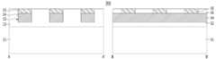
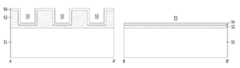
도 4a 내지 도 4j는 본 발명의 제2실시예에 따른 반도체 장치를 제조하기 위한 제조방법의 일례를 도시한 공정단면도이다. 여기서, 도 4a 내지 도 4j는 도 3a에 도시된 A-A'절취선을 따라 도시한 것이다.4A to 4J are process cross-sectional views showing an example of a manufacturing method for manufacturing a semiconductor device according to the second embodiment of the present invention. 4A to 4J are taken along the line AA ′ of FIG. 3A.
도 4a에 도시된 바와 같이, 기판(51)에 불순물을 이온주입하여 펀치쓰루방지층(52)을 형성한다. 펀치쓰루방지층(52)은 후속 공정을 통해 형성될 매립비트라인 사이의 펀치쓰루 및 매립비트라인과 기판(51) 사이의 펀치쓰루를 방지하는 역할을 수행하는 것으로, 불순물을 기판(51)에 이온주입하여 형성할 수 있다. 이때, 불순물은 P형 불순물일 수 있다.As shown in FIG. 4A, the punch-through
다음으로, 기판(51)상에 감광막패턴(미도시)을 형성한 후에 감광막패턴을 식각장벽으로 기판(51)을 식각하여 다수의 제1트렌치(53)를 형성한다. 이때, 제1트렌치(53)는 후속 공정에서 매립비트라인과 제1소스/드레인층이 형성될 공간을 제공하기 위한 것이다. 제1트렌치(53)는 일방향 예컨대, 매립비트라인이 연장되는 방향(B-B'방향)으로 연장된 라인타입의 패턴으로 형성할 수 있다. 그리고, 펀치쓰루방지층(52)의 특성을 최적화하기 위하여 기판(51) 표면을 기준으로 제1트렌치(53)의 깊이는 펀치쓰루방지층(52)의 깊이보다 작은 것이 바람직하다.Next, after the photoresist pattern (not shown) is formed on the
다음으로, 펀치쓰루방지층(52)과 더불어서 인접한 매립비트라인 사이 및 매립비트라인과 기판(51) 사이를 전기적으로 분리시키기 위하여 제1트렌치(53)를 포함한 기판(51) 표면을 따라 제1절연막(54)을 형성한다. 제1절연막(54)은 산화막, 질화막 및 산화질화막으로 이루어진 그룹으로부터 선택된 어느 하나로 형성할 수 있다.Next, a first insulating film along the surface of the
도 4b에 도시된 바와 같이, 제1트렌치(53)를 일부 매립하는 매립비트라인(55)을 형성한다. 매립비트라인(55)은 신호전달특성을 향상시키기 위하여 금속성막으로 형성한다. 구체적으로, 매립비트라인(55)은 금속막, 금속질화막, 금속산화막 및 금속실리사이드막으로 이루어진 그룹으로부터 선택된 어느 하나 또는 둘 이상이 적층된 적층막으로 형성할 수 있다. 제1트렌치(53)를 일부 매립하는 매립비트라인(55)는 제1트렌치(53)를 매립하도록 기판(51) 전면에 금속성막을 증착한 이후에 금속성막에 대한 전면식각 예컨대, 에치백을 실시하는 일련의 공정과정을 통해 형성할 수 있다.As shown in FIG. 4B, a buried
다음으로, 매립비트라인(55) 상에 나머지 제1트렌치(53)를 매립하는 제1소스/드레인층(56)을 형성한다. 제1소스/드레인층(56)은 불순물이 도핑되고, 다결정상태 또는 단결정상태를 갖는 반도체막으로 형성할 수 있다. 이때, 반도체막은 실리콘함유막일 수 있으며, 실리콘함유막은 실리콘막(Si), 실리콘저마늄막(SiGe) 및 실리콘카본막(SiC)으로 이루어진 그룹으로부터 선택된 어느 하나일 수 있다. 제1소스/드레인층(56)은 후속 공정을 통해 형성될 트랜지스터에서 접합영역으로 작용하기 때문에 제1소스/드레인층(56)을 형성함과 동시에 제1소스/드레인층(56)에 불순물을 도핑시키거나, 또는 제1소스/드레인층(56)을 형성한 이후에 불순물을 도핑시킬 수 있다. 일례로, 제1소스/드레인층(56)은 N형 불순물로 도핑될 수 있다.Next, the first source /
제1트렌치(53)를 매립하는 제1소스/드레인층(56)은 기판(51) 전면에 반도체막을 형성한 이후에 제1절연막(54)이 노출될때까지 평탄화공정을 실시하는 일련의 공정과정을 통해 형성할 수 있다. 이때, 평탄화공정은 화학적기계적연마법(CMP)으로 사용하여 실시할 수 있다.The first source /
한편, 제1소스/드레인층(56)을 형성하기 이전에 매립비트라인(55)과 제1소스/드레인층(56) 사이의 확산을 방지하는 도전성 확산방지막(미도시)을 형성하거나, 매립비트라인(55)과 제1소스/드레인층(56) 사이의 콘택저항을 감소시키기 위한 오믹콘택층(미도시) 형성할 수도 있다. 물론, 도전성 확산방지막과 오믹콘택층이 적층된 적층막을 매립비트라인(55)과 제1소스/드레인층(56) 사이에 형성할 수도 있다.Meanwhile, before forming the first source /
다음으로, 후속 공정을 통해 형성될 적층패턴에 대응하도록 제1소스/드레인층(56)을 선택적으로 식각한다. 적층패턴에 대응하도록 식각된 제1소스/드레인층(56)은 매립비트라인(55) 상에서 매트릭스 배열구조를 갖는다. 즉, 제1소스/드레인층(56)을 적층패턴에 대응하도록 식각한 이후에는 매립비트라인(55)이 연장된 방향으로 제1소스/드레인층(56)이 불연속적으로 배치된 형태를 갖는다.Next, the first source /
다음으로, 매립비트라인(55) 상에 식각된 제1소스/드레인층(56) 사이를 매립하는 제2절연막(57)을 형성한다. 제2절연막(57)은 인접한 제1소스/드레인층(56) 사이를 전기적으로 분리시킴과 동시에 후속 공정간 매립비트라인(55)을 보호하는 역할을 수행한다. 또한, 후속 공정을 통해 형성될 워드라인과 매립비트라인(55) 사이를 전기적으로 분리시키는 역할도 수행한다. 제2절연막(57)은 산화막, 질화막 및 산화질화막으로 이루어진 그룹으로부터 선택된 어느 하나로 형성할 수 있으며, 제1절연막(54)과 동일한 물질로 형성할 수 있다.Next, a second insulating
이하, 설명의 편의를 위하여 기판(51), 펀치쓰루방지층(52), 제1트렌치(53), 제1절연막(54), 매립비트라인(55), 제1소스/드레인층(56) 및 제2절연막(57)을 포함하는 제1구조물을 '제1웨이퍼(500)'라 표기하기로 한다.Hereinafter, for convenience of description, the
도 4c에 도시된 바와 같이, 스플리팅층(62)이 형성된 희생기판(61) 상에 제2소스/드레인층(63)과 채널층(64)을 순차적으로 형성한다. 스플리팅층(62)은 후속 클리빙공정(cleaving process)시 본딩된 두 웨이퍼를 분리시키기 위한 것으로, 희생기판(61)에 기화성 물질(예컨대, 수소)을 이온주입하여 형성할 수 있다. 참고로, 스플리팅층(62)은 제2소스/드레인층(63)과 채널층(64)을 형성하기 이전에 형성하거나, 또는 이들을 형성한 이후에 형성할 수 있다.As shown in FIG. 4C, the second source /
제2소스/드레인층(63) 및 채널층(64)은 불순물이 도핑되고, 다결정상태 또는 단결정상태를 갖는 반도체막으로 형성할 수 있다. 이때, 반도체막은 실리콘함유막일 수 있으며, 실리콘함유막은 실리콘막(Si), 실리콘저마늄막(SiGe) 및 실리콘카본막(SiC)으로 이루어진 그룹으로부터 선택된 어느 하나로 형성할 수 있다. 여기서, 트랜지스터의 동작특성을 제어하기 위하여 채널층(64), 제1 및 제2소스/드레인층(56, 63)은 모두 동일한 반도체 물질로 형성하거나, 또는 모두 상이한 반도체 물질로 형성할 수도 있다. 또한, 제1 및 제2소스/드레인층(56, 63)은 서로 동일한 반도체 물질로 형성하고, 채널층(64)은 제1 및 제2소스/드레인층(56, 63)과는 상이한 반도체 물질로 형성할 수 있다.The second source /
또한, 채널층(64)은 후속 공정을 통해 형성될 트랜지스터에서 채널영역으로 작용하고, 제2소스/드레인층(63)은 트랜지스터의 접합영역으로 작용하기 때문에 제2소스/드레인층(63) 및 채널층(64)은 이들은 형성함과 동시에 불순물을 도핑시키거나, 또는 이들을 형성한 이후에 불순물을 도핑시킬 수 있다. 제1 및 제2소스/드레인층(56, 63)은 서로 동일한 도전형을 갖도록 불순물을 도핑시킬 수 있고, 채널층(64)은 제1 및 제2소스/드레인층(56, 63)과 서로 상보적인 도전형을 갖도록 도핑시킬 수 있다. 일례로, 제1 및 제2소스/드레인층(56, 63)에는 N형 불순물을 도핑시킬 수 있고, 채널층(64)에는 P형 불순물을 도핑시킬 수 있다.In addition, since the
도 4d에 도시된 바와 같이, 채널층(64) 상에 제1하드마스크패턴(65)을 형성한 후에 제1하드마스크패턴(65)을 식각장벽으로 채널층(64) 및 제2소스/드레인층(63)을 순차적으로 식각하여 적층패턴(66)을 형성한다. 이때, 적층패턴(66)은 필라타입의 패턴으로 형성할 수 있고, 인접한 적층패턴(66)과 일정간격 이격된 매트릭스 배열구조를 갖도록 형성할 수 있다.As shown in FIG. 4D, after the first
도 4e에 도시된 바와 같이, 제1하드마스크패턴(65)을 제거한 이후에 적층패턴(66) 사이를 갭필하는 제3절연막(67)을 형성한다. 제3절연막(67)은 적층패턴(66)을 포함한 희생기판(61) 전면에 제3절연막(67)을 형성한 이후에 채널층(64)이 노출될때까지 평탄화공정을 실시하는 일련의 공정과정을 통해 형성할 수 있다. 제3절연막(67)은 산화막, 질화막 및 산화질화막으로 이루어진 그룹으로부터 선택된 어느 하나로 형성할 수 있고, 평탄화공정은 화학적기계적연마법을 사용하여 실시할 수 있다. 한편, 평탄화공정시 제1하드마스크패턴(65)을 제거할 수도 있다.As shown in FIG. 4E, after removing the first
다음으로, 제3절연막(67) 상에 제2하드마스크패턴(68)을 형성한다, 제2하드마스크패턴(68)은 워드라인을 형성하기 위한 것으로, 매립비트라인(55)이 연장된 방향과 교차하는 방향으로 연장된 라인타입의 패턴으로 형성할 수 있다.Next, a second
도 4f에 도시된 바와 같이, 제2하드마스크패턴(68)을 식각장벽으로 제3절연막(67)을 리세스식각(recess etch)하여 일방향으로 배치된 적층패턴(66)의 채널층(64) 측벽을 노출시키는 제2트렌치(69)를 형성한다. 이때, 제2하드마스크패턴(68)의 형태에 따라 제2트렌치(69)은 라인타입의 패턴일 수 있으며, 채널층(64)의 일측벽을 노출시키는 구조, 채널층(64)의 양측벽을 노출시키는 구조 또는 채널층(64)의 모든 측벽을 노출시키는 구조로 형성할 수 있다.As shown in FIG. 4F, the
다음으로, 제2하드마스크패턴(68)을 제거한다.Next, the second
도 4g에 도시된 바와 같이, 제2트렌치(69)에 의하여 노출된 채널층(64) 표면에 게이트절연막(70)을 형성한다. 게이트절연막(70)은 산화법(예컨대, 열산화법) 또는 증착법(예컨대, 화학기상증착법)을 사용하여 형성할 수 있다. 또한, 게이트절연막(70)은 산화법을 사용하여 일정 두께를 형성한 이후에 나머지 두께는 증착법을 사용하여 형성할 수도 있다.As shown in FIG. 4G, the
다음으로, 제2트렌치(69)을 매립하도록 희생기판(61) 전면에 도전막(71)을 형성한다. 이때, 도전막(71)은 금속성막으로 형성할 수 있다. 구체적으로, 도전막(71)은 금속막, 금속질화막, 금속산화막 및 금속실리사이드막으로 이루어진 그룹으로부터 선택된 어느 하나 또는 둘 이상이 적층된 적층막으로 형성할 수 있다.Next, a
도 4h에 도시된 바와 같이, 도전막(71)을 선택적으로 식각하여 제2트렌치(69)를 일부 매립하는 워드라인(71A)을 형성한다. 즉, 워드라인(71A) 형성공정이 완료된 시점에서 워드라인(71A)의 표면이 채널층(64)의 표면보다 낮도록 도전막(71)을 식각한다. 식각공정은 전면식각법 예컨대, 에치백을 사용하여 실시할 수 있다.As shown in FIG. 4H, the
다음으로, 워드라인(71A)을 포함한 구조물 전면에 제4절연막(72)을 형성한 후에 채널층(64)이 노출될때까지 평탄화공정을 실시한다. 제4절연막(72)은 후속 웨이퍼 본딩 공정시 오정렬에 의하여 워드라인(72)과 제1소스/드레인층(56) 사이에 쇼트가 발생하는 것을 방지하는 역할을 수행하는 것으로, 산화막, 질화막 및 산화질화막으로 이루어진 그룹으로부터 선택된 어느 하나로 형성할 수 있다. 그리고, 평탄화공정은 화학적기계적연마법을 사용하여 실시할 수 있다.Next, after the fourth insulating
이하, 설명의 편의를 위하여 스플리팅층(62)이 형성된 희생기판(61), 적층패턴(66) 및 워드라인(71A)을 포함하는 제2구조물을 '제2웨이퍼(600)'라 표기하기로 한다.Hereinafter, for convenience of description, the second structure including the
도 4i에 도시된 바와 같이, 제1웨이퍼(500)에서 제1소스/드레인층(56)이 노출된 표면과 제2웨이퍼(600)에서 채널층(64)이 노출된 표면이 서로 마주보도록 정렬시킨 이후에 제1소스/드레인층(56)과 적층패턴(66)의 채널층(64)이 서로 접하고, 매립비트라인(55)과 워드라인(71A)이 교차하도록 제1웨이퍼(500)와 제2웨이퍼(600)를 본딩한다. 이때, 웨이퍼 본딩은 공지된 다양한 기술을 사용하여 실시할 수 있으며, 제1 및 제2웨이퍼(500, 600)를 본딩하기 이전에 이들 사이의 접착력을 향상시키기 위하여 소정의 표면처리를 실시할 수 있다.As shown in FIG. 4I, the surface on which the first source /
도 4j에 도시된 바와 같이, 스플리팅층(62)에 물리적 충격을 인가하여 희생기판(61)을 제거하는 클리빙공정을 실시한다. 이때, 클리빙공정은 공지된 다양한 기술을 사용하여 실시할 수 있다.As shown in FIG. 4J, a cleaving process is performed to remove the
다음으로, 클리빙공정 이후에 잔류하는 잔류물을 제거한다. 예컨대, 제2소스/드레인층(63)의 표면이 노출될때까지 평탄화공정을 실시하여 클리빙공정 이후에 잔류하는 스플리팅층(62) 및 희생기판(61)을 제거하고, 연속해서 세정공정을 실시할 수 있다.Next, residues remaining after the cleaving process are removed. For example, the planarization process is performed until the surface of the second source /
다음으로, 기판(51) 전면에 층간절연막(81)을 형성한 후에 층간절연막(81)을 관통하여 제2소스/드레인층(63)에 연결되는 스토리지노드콘택플러그(82)를 형성한다. 이때, 층간절연막(81)을 형성하는 이유는 후속 공정을 통해 형성될 스토리지노드(83)와 워드라인(71A) 사이의 충분한 간격이 확보되지 않아 스토리지노드(83) 형성공정에 대한 마진이 감소하거나, 이들 사이의 간섭에 의하여 동작특성이 열화되는 것을 방지하기 위함이다.Next, after the
다음으로, 층간절연막(81) 상에 스토리지노드콘택플러그(82)에 접하는 스토리지노드(83), 스토리지노드(83) 상의 유전막(84) 및 유전막(84) 상의 플레이트 전극(85)를 순차적으로 형성하여 매립비트라인(55)을 구비하는 수직 채널 반도체 장치를 완성한다.Next, the
상술한 본 발명의 실시예에 따른 반도체 장치 제조방법에 따르면, 매립비트라인(55)을 금속성막으로 형성함으로서 저저항 매립비트라인(55)을 구현할 수 있고, 매립비트라인(55)이 형성된 기판(51)에 적층패턴(66)을 본딩함으로서 저저항 매립비트라인(55)을 손쉽게 형성할 수 있다.According to the semiconductor device manufacturing method according to the embodiment of the present invention described above, by forming the buried
또한, 매립비트라인(55)과 적층패턴(66)를 본딩하여 수직 채널 반도체 장치를 구현함으로서, 각각의 구조가 단순하여 집적도를 용이하게 향상시킬 수 있고, 공정과정을 단순화시킬 수 있으며, 공정난이도를 감소시켜 양산에 적용하기 용이하다. 아울러, 인접한 매립비트라인(55) 사이의 캐패시턴스를 감소시킬 수도 있다.
In addition, by implementing the vertical channel semiconductor device by bonding the buried
본 발명의 기술 사상은 상기 바람직한 실시예에 따라 구체적으로 기술되었으나, 상기 실시예는 그 설명을 위한 것이며, 그 제한을 위한 것이 아님을 주의하여야 한다. 또한, 본 발명의 기술분야의 통상의 전문가라면 본 발명의 기술사상의 범위내의 다양한 실시예가 가능함을 이해할 수 있을 것이다.
The technical idea of the present invention has been specifically described according to the above preferred embodiments, but it should be noted that the above embodiments are intended to be illustrative and not restrictive. In addition, it will be understood by those of ordinary skill in the art that various embodiments within the scope of the technical idea of the present invention are possible.
101 : 기판102 : 제1절연막
103 : 트렌치104 : 매립비트라인
105 : 제1소스/드레인층106 : 제2절연막
107 : 채널층108 : 제2소스/드레인층
109 : 적층패턴110 : 하드마스크패턴
111 : 게이트절연막112 : 워드라인
113 : 제3절연막114 : 스토리지노드콘택플러그
115 : 스토리지노드116 : 유전막
117 : 플레이트 전극101
103: trench 104: buried bit line
105: first source / drain layer 106: second insulating film
107: channel layer 108: second source / drain layer
109: laminated pattern 110: hard mask pattern
111: gate insulating film 112: word line
113: third insulating film 114: storage node contact plug
115: storage node 116: dielectric film
117: plate electrode
Claims (27)
Translated fromKorean상기 트렌치를 일부 매립하는 매립비트라인;
상기 매립비트라인 상의 나머지 상기 트렌치를 매립하는 제1소스/드레인층;
채널층과 제2소스/드레인층이 적층된 구조를 갖고, 상기 채널층이 상기 제1소스/드레인층에 접하도록 상기 제1소스/드레인층에 본딩된 적층패턴; 및
상기 매립비트라인과 교차하고, 상기 채널층의 측벽에 접하는 워드라인
을 포함하는 반도체 장치.
A trench formed in the substrate;
A buried bit line filling a portion of the trench;
A first source / drain layer filling the remaining trench on the buried bit line;
A stacked pattern having a structure in which a channel layer and a second source / drain layer are laminated, and bonded to the first source / drain layer such that the channel layer contacts the first source / drain layer; And
A word line crossing the buried bit line and in contact with a sidewall of the channel layer
≪ / RTI >
상기 기판은 상기 기판상의 절연막을 더 포함하고,
상기 트렌치는 상기 절연막에 형성된 반도체 장치.
The method of claim 1,
The substrate further includes an insulating film on the substrate,
And the trench is formed in the insulating film.
상기 기판에 형성된 펀치쓰루방지층; 및
상기 트렌치 표면에 형성된 절연막을 더 포함하는 반도체 장치.
The method of claim 1,
A punchthrough prevention layer formed on the substrate; And
And an insulating film formed on the trench surface.
상기 트렌치는 상기 펀치쓰루방지층에 형성된 반도체 장치.
The method of claim 3,
And the trench is formed in the punch-through prevention layer.
상기 제1소스/드레인층의 표면과 상기 기판의 표면은 동일면상이 위치하는 반도체 장치.
The method of claim 1,
And the surface of the first source / drain layer and the surface of the substrate are coplanar.
상기 적층패턴은 필라타입의 패턴으로,
매트릭스 배열구조를 갖는 반도체 장치.
The method of claim 1,
The laminated pattern is a pillar type pattern,
A semiconductor device having a matrix array structure.
상기 제1소스/드레인층은 상기 적층패턴에 대응하는 매트릭스 배열구조를 갖는 반도체 장치.
The method according to claim 6,
And the first source / drain layer has a matrix array structure corresponding to the stacked pattern.
상기 매립비트라인이 연장된 방향으로 상기 매립비트라인 상에서 상기 제1소스/드레인층 사이의 나머지 상기 트렌치에 매립된 절연막을 더 포함하는 반도체 장치.
The method of claim 7, wherein
And an insulating film embedded in the remaining trench between the first source / drain layer on the buried bit line in a direction in which the buried bit line extends.
상기 채널층과 상기 워드라인 사이에 삽입된 게이트절연막을 더 포함하는 반도체 장치.
The method of claim 1,
And a gate insulating film interposed between the channel layer and the word line.
상기 게이트절연막은 상기 워드라인 하부면까지 확장된 반도체 장치.
10. The method of claim 9,
And the gate insulating layer is extended to a lower surface of the word line.
채널층과 제2소스/드레인층이 적층된 적층패턴, 상기 적층패턴 사이를 갭필하는 절연막, 상기 절연막에 형성되어 상기 채널층의 측벽을 노출시키는 제2트렌치 및 상기 제2트렌치에 매립된 워드라인을 포함하는 제2구조물을 포함하고,
상기 매립비트라인과 상기 워드라인이 교차하고, 상기 제1소스/드레인층과 상기 채널층이 접하도록 상기 제1구조물과 상기 제2구조물이 본딩된 반도체 장치.
A first structure including a first trench formed in a substrate, a buried bit line filling a portion of the first trench, and a first source / drain layer filling the remaining first trench on the buried bit line; And
A stack pattern in which a channel layer and a second source / drain layer are stacked, an insulating film gap gap between the stacked patterns, a second trench formed in the insulating film to expose sidewalls of the channel layer, and a word line embedded in the second trench Including a second structure comprising a,
And the first structure and the second structure are bonded such that the buried bit line and the word line cross each other and the first source / drain layer and the channel layer contact each other.
상기 기판은 상기 기판상의 절연막을 더 포함하고,
상기 제1트렌치는 상기 절연막에 형성된 반도체 장치.
12. The method of claim 11,
The substrate further includes an insulating film on the substrate,
And the first trench is formed in the insulating film.
상기 기판에 형성된 펀치쓰루방지층; 및
상기 제1트렌치 표면에 형성된 절연막을 더 포함하는 반도체 장치.
12. The method of claim 11,
A punchthrough prevention layer formed on the substrate; And
And an insulating film formed on the surface of the first trench.
상기 제1트렌치는 상기 펀츠쓰루방지층에 형성된 반도체 장치.
The method of claim 13,
And the first trench is formed in the puncturing prevention layer.
상기 제1소스/드레인층의 표면과 상기 기판의 표면은 동일면상이 위치하는 반도체 장치.
12. The method of claim 11,
And the surface of the first source / drain layer and the surface of the substrate are coplanar.
상기 적층패턴은 필라타입의 패턴으로,
매트릭스 배열구조를 갖는 반도체 장치.
12. The method of claim 11,
The laminated pattern is a pillar type pattern,
A semiconductor device having a matrix array structure.
상기 제1소스/드레인층은 상기 적층패턴에 대응하는 매트릭스 배열구조를 갖는 반도체 장치.
17. The method of claim 16,
And the first source / drain layer has a matrix array structure corresponding to the stacked pattern.
상기 매립비트라인이 연장된 방향으로 상기 매립비트라인 상에서 상기 제1소스/드레인층 사이의 나머지 상기 제1트렌치에 매립된 절연막을 더 포함하는 반도체 장치.
18. The method of claim 17,
And an insulating film embedded in the first trench remaining between the first source / drain layer on the buried bit line in a direction in which the buried bit line extends.
상기 워드라인은 상기 제2트렌치를 일부 매립하는 형태를 갖고,
상기 워드라인 상에서 나머지 상기 제2트렌치를 매립하는 절연막을 더 포함하는 반도체 장치.
12. The method of claim 11,
The word line has a form of partially filling the second trench,
And an insulating film filling the second trench on the word line.
상기 트렌치를 일부 매립하는 매립비트라인을 형성하는 단계;
상기 매립비트라인 상에 나머지 상기 트렌치를 매립하는 제1소스/드레인층을 형성하는 단계;
희생기판 전면에 제2소스/드레인층과 채널층을 순차적으로 형성하는 단계;
상기 제1소스/드레인층과 상기 채널층이 서로 마주보도록 상기 기판과 상기 희생기판을 본딩하는 단계;
상기 희생기판을 제거하는 클리빙공정을 실시하는 단계;
상기 제2소스/드레인층 및 상기 채널층을 선택적으로 식각하여 적층패턴을 형성하되, 상기 채널층이 상기 제1소스/드레인층과 접하도록 형성하는 단계; 및
상기 매립비트라인과 교차하고, 상기 채널층 측벽에 접하는 워드라인을 형성하는 단계
를 포함하는 반도체 장치 제조방법.
Forming a trench in the substrate;
Forming a buried bit line filling a portion of the trench;
Forming a first source / drain layer filling the remaining trench on the buried bit line;
Sequentially forming a second source / drain layer and a channel layer on the entire surface of the sacrificial substrate;
Bonding the substrate and the sacrificial substrate such that the first source / drain layer and the channel layer face each other;
Performing a cleaving process to remove the sacrificial substrate;
Selectively etching the second source / drain layer and the channel layer to form a stacked pattern, wherein the channel layer is in contact with the first source / drain layer; And
Forming a word line crossing the buried bit line and in contact with the sidewall of the channel layer;
≪ / RTI >
상기 적층패턴은 필라타입의 패턴으로 매트릭스 배열구조를 갖도록 형성하는 반도체 장치 제조방법.
21. The method of claim 20,
The stacked pattern is a semiconductor device manufacturing method of forming a matrix array structure in a pillar-shaped pattern.
상기 제1소스/드레인층은 상기 적층패턴에 대응하여 매트릭스 배열구조를 갖도록 형성하고,
상기 제1소스/드레인층을 형성한 이후에 상기 매립비트라인이 연장된 방향으로 상기 제1소스/드레인층 사이의 나머지 상기 트렌치를 매립하는 절연막을 형성하는 단계를 더 포함하는 반도체 장치 제조방법.
The method of claim 21,
The first source / drain layer may be formed to have a matrix array structure corresponding to the stacked pattern.
And forming an insulating layer filling the remaining trench between the first source / drain layers in a direction in which the buried bit line extends after forming the first source / drain layer.
상기 워드라인을 형성하기 이전에 상기 적층패턴을 포함한 구조물 표면에 게이트절연막을 형성하는 단계를 더 포함하는 반도체 장치 제조방법.
21. The method of claim 20,
And forming a gate insulating film on a surface of the structure including the stacked pattern before forming the word line.
상기 제1트렌치를 일부 매립하는 매립비트라인을 형성하는 단계;
상기 매립비트라인 상에 나머지 상기 제1트렌치를 매립하는 제1소스/드레인층을 형성하는 단계;
희생기판 상에 제2소스/드레인층과 채널층이 적층된 적층패턴을 형성하는 단계;
상기 희생기판 상에 상기 적층패턴 사이를 매립하고, 상기 채널층의 측벽을 노출시키는 제2트렌치를 구비한 절연막을 형성하는 단계;
상기 제2트렌치를 매립하는 워드라인을 형성하는 단계;
상기 매립비트라인과 상기 워드라인이 서로 교차하고, 상기 제1소스/드레인층과 상기 채널층이 서로 접하도록 상기 기판과 상기 희생기판을 본딩하는 단계; 및
상기 희생기판을 제거하는 클리빙공정을 실시하는 단계
를 포함하는 반도체 장치 제조방법.
Forming a first trench in the substrate;
Forming a buried bit line filling a portion of the first trench;
Forming a first source / drain layer filling the remaining first trench on the buried bit line;
Forming a stacked pattern in which a second source / drain layer and a channel layer are stacked on the sacrificial substrate;
Forming an insulating film on the sacrificial substrate, the insulating layer having a second trench filling the sidewalls of the channel layer and filling the sidewalls of the channel layer;
Forming a word line filling the second trench;
Bonding the substrate and the sacrificial substrate so that the buried bit line and the word line cross each other and the first source / drain layer and the channel layer contact each other; And
Performing a cleaving process to remove the sacrificial substrate
≪ / RTI >
상기 적층패턴은 필라타입의 패턴으로 매트릭스 배열구조를 갖도록 형성하는 반도체 장치 제조방법.
25. The method of claim 24,
The stacked pattern is a semiconductor device manufacturing method of forming a matrix array structure in a pillar-shaped pattern.
상기 제1소스/드레인층은 상기 적층패턴에 대응하여 매트릭스 배열구조를 갖도록 형성하고,
상기 제1소스/드레인층을 형성한 이후에 상기 매립비트라인이 연장된 방향으로 상기 제1소스/드레인층 사이의 나머지 상기 제1트렌치를 매립하는 절연막을 형성하는 단계를 더 포함하는 반도체 장치 제조방법.
26. The method of claim 25,
The first source / drain layer may be formed to have a matrix array structure corresponding to the stacked pattern.
After forming the first source / drain layer, forming an insulating layer to fill the remaining first trench between the first source / drain layer in a direction in which the buried bit line extends. Way.
상기 워드라인은 상기 제2트렌치를 일부 매립하도록 형성하고,
상기 워드라인을 형성한 이후에 상기 워드라인 상에 나머지 상기 제2트렌치를 매립하는 절연막을 형성하는 단계를 더 포함하는 반도체 장치 제조방법.25. The method of claim 24,
The word line is formed to partially fill the second trench,
And forming an insulating layer filling the second trench on the word line after forming the word line.
Priority Applications (4)
| Application Number | Priority Date | Filing Date | Title |
|---|---|---|---|
| KR20120024914AKR20130103908A (en) | 2012-03-12 | 2012-03-12 | Semiconductor device with buried bit line and method for fabricating the same |
| US13/554,739US8643096B2 (en) | 2012-03-12 | 2012-07-20 | Semiconductor device with buried bit line and method for fabricating the same |
| US14/145,430US8921930B2 (en) | 2012-03-12 | 2013-12-31 | Semiconductor device with buried bit line and method for fabricating the same |
| US14/550,351US9087856B2 (en) | 2012-03-12 | 2014-11-21 | Semiconductor device with buried bit line and method for fabricating the same |
Applications Claiming Priority (1)
| Application Number | Priority Date | Filing Date | Title |
|---|---|---|---|
| KR20120024914AKR20130103908A (en) | 2012-03-12 | 2012-03-12 | Semiconductor device with buried bit line and method for fabricating the same |
Publications (1)
| Publication Number | Publication Date |
|---|---|
| KR20130103908Atrue KR20130103908A (en) | 2013-09-25 |
Family
ID=49113328
Family Applications (1)
| Application Number | Title | Priority Date | Filing Date |
|---|---|---|---|
| KR20120024914AWithdrawnKR20130103908A (en) | 2012-03-12 | 2012-03-12 | Semiconductor device with buried bit line and method for fabricating the same |
Country Status (2)
| Country | Link |
|---|---|
| US (3) | US8643096B2 (en) |
| KR (1) | KR20130103908A (en) |
Cited By (1)
| Publication number | Priority date | Publication date | Assignee | Title |
|---|---|---|---|---|
| KR20200117926A (en)* | 2020-09-23 | 2020-10-14 | 삼성전자주식회사 | Semiconductor memory device and manufacturing method thereof |
Families Citing this family (34)
| Publication number | Priority date | Publication date | Assignee | Title |
|---|---|---|---|---|
| KR20130139599A (en)* | 2012-06-13 | 2013-12-23 | 에스케이하이닉스 주식회사 | Semiconductor device, electronic system and manufacturing method for the same |
| US9245893B1 (en)* | 2014-11-19 | 2016-01-26 | Micron Technology, Inc. | Semiconductor constructions having grooves dividing active regions |
| US10121553B2 (en) | 2015-09-30 | 2018-11-06 | Sunrise Memory Corporation | Capacitive-coupled non-volatile thin-film transistor NOR strings in three-dimensional arrays |
| US11120884B2 (en) | 2015-09-30 | 2021-09-14 | Sunrise Memory Corporation | Implementing logic function and generating analog signals using NOR memory strings |
| KR102337640B1 (en)* | 2017-04-25 | 2021-12-13 | 삼성전자주식회사 | Three Dimensional Semiconductor Devices |
| US10217748B2 (en)* | 2017-05-25 | 2019-02-26 | Winbond Electronics Corp. | Dynamic random access memory and method of manufacturing the same |
| CN109461756B (en) | 2017-09-06 | 2021-05-14 | 中国科学院微电子研究所 | MRAM, method of manufacturing the same, and electronic device including the same |
| CN109461738B (en) | 2017-09-06 | 2021-03-26 | 中国科学院微电子研究所 | Semiconductor memory device, method of manufacturing the same, and electronic device including the same |
| US12317511B2 (en)* | 2017-09-06 | 2025-05-27 | Institute of Microelectronics, Chinese Academy of Sciences | MRAM, method of manufacturing the same, and electronic device including the MRAM |
| US10522686B2 (en)* | 2017-09-26 | 2019-12-31 | International Business Machines Corporation | Vertical thin film transistor |
| WO2019132999A1 (en)* | 2017-12-29 | 2019-07-04 | Intel Corporation | Integrated circuit structures with vertical architecture |
| US11653487B2 (en)* | 2018-06-20 | 2023-05-16 | Intel Corporation | 4F2 DRAM cell using vertical thin film transistor |
| TWI683418B (en)* | 2018-06-26 | 2020-01-21 | 華邦電子股份有限公司 | Dynamic random access memory and methods of manufacturing, reading and writing the same |
| US11751391B2 (en) | 2018-07-12 | 2023-09-05 | Sunrise Memory Corporation | Methods for fabricating a 3-dimensional memory structure of nor memory strings |
| CN109285838B (en)* | 2018-08-28 | 2023-05-02 | 中国科学院微电子研究所 | Semiconductor memory device, method of manufacturing the same, and electronic apparatus including the same |
| US11417770B2 (en)* | 2018-09-26 | 2022-08-16 | Intel Corporation | Vertical thin-film transistors between metal layers |
| US11437273B2 (en)* | 2019-03-01 | 2022-09-06 | Micromaterials Llc | Self-aligned contact and contact over active gate structures |
| WO2021127218A1 (en)* | 2019-12-19 | 2021-06-24 | Sunrise Memory Corporation | Process for preparing a channel region of a thin-film transistor |
| TWI836184B (en) | 2020-02-07 | 2024-03-21 | 美商森恩萊斯記憶體公司 | High capacity memory circuit with low effective latency |
| CN113540088B (en)* | 2020-04-16 | 2024-02-13 | 长鑫存储技术有限公司 | Memory structure and forming method thereof |
| CN113644064B (en) | 2020-04-27 | 2023-09-12 | 长鑫存储技术有限公司 | Semiconductor structure and method of forming the same, memory and method of forming the same |
| US11937424B2 (en) | 2020-08-31 | 2024-03-19 | Sunrise Memory Corporation | Thin-film storage transistors in a 3-dimensional array of nor memory strings and process for fabricating the same |
| EP4340563A4 (en)* | 2021-07-09 | 2024-10-30 | Changxin Memory Technologies, Inc. | PREPARATION METHOD FOR SEMICONDUCTOR STRUCTURE, AND SEMICONDUCTOR STRUCTURE |
| CN114121959B (en)* | 2021-11-19 | 2024-11-26 | 北京超弦存储器研究院 | Storage device and manufacturing method thereof, and electronic device including the storage device |
| CN116525543B (en)* | 2022-01-19 | 2024-12-06 | 长鑫存储技术有限公司 | Semiconductor structure and method for manufacturing the same |
| KR20230140962A (en)* | 2022-03-30 | 2023-10-10 | 삼성전자주식회사 | Semiconductor device including vertical channel region |
| CN114927477A (en)* | 2022-05-06 | 2022-08-19 | 长鑫存储技术有限公司 | Preparation method of semiconductor device, semiconductor device and stacked device |
| CN117177557A (en)* | 2022-05-24 | 2023-12-05 | 长鑫存储技术有限公司 | Semiconductor structure and manufacturing method thereof |
| CN117457737A (en)* | 2022-10-17 | 2024-01-26 | 北京超弦存储器研究院 | Method for forming buried bit lines, memory and method of manufacturing same |
| WO2024103343A1 (en)* | 2022-11-17 | 2024-05-23 | Yangtze Memory Technologies Co., Ltd. | Vertical transistors and methods for forming the same |
| CN118695577A (en)* | 2023-03-21 | 2024-09-24 | 北京超弦存储器研究院 | Semiconductor device and manufacturing method thereof, and electronic device |
| CN116648058B (en)* | 2023-04-24 | 2024-04-09 | 北京超弦存储器研究院 | Semiconductor device, manufacturing method thereof and electronic equipment |
| KR20250061539A (en)* | 2023-10-27 | 2025-05-08 | 에스케이하이닉스 주식회사 | Semiconductor dedvice and method for fabricating the same |
| CN120547936A (en)* | 2025-07-28 | 2025-08-26 | 西湖大学 | A method for preparing a drive array, a drive array, and an electronic device |
Family Cites Families (4)
| Publication number | Priority date | Publication date | Assignee | Title |
|---|---|---|---|---|
| KR101116353B1 (en)* | 2009-12-30 | 2012-03-09 | 주식회사 하이닉스반도체 | Semiconductor device with vertical cell and mehtod for manufacturing the same |
| KR20110078063A (en) | 2009-12-30 | 2011-07-07 | 주식회사 하이닉스반도체 | Semiconductor device with buried bit line and manufacturing method thereof |
| US8956961B2 (en)* | 2012-03-09 | 2015-02-17 | Rexchip Electronics Corporation | Semiconductor device and method for making the same |
| KR20130106159A (en)* | 2012-03-19 | 2013-09-27 | 에스케이하이닉스 주식회사 | Semiconductor device having buried bitline and fabricating the same |
- 2012
- 2012-03-12KRKR20120024914Apatent/KR20130103908A/ennot_activeWithdrawn
- 2012-07-20USUS13/554,739patent/US8643096B2/enactiveActive
- 2013
- 2013-12-31USUS14/145,430patent/US8921930B2/enactiveActive
- 2014
- 2014-11-21USUS14/550,351patent/US9087856B2/enactiveActive
Cited By (1)
| Publication number | Priority date | Publication date | Assignee | Title |
|---|---|---|---|---|
| KR20200117926A (en)* | 2020-09-23 | 2020-10-14 | 삼성전자주식회사 | Semiconductor memory device and manufacturing method thereof |
Also Published As
| Publication number | Publication date |
|---|---|
| US8921930B2 (en) | 2014-12-30 |
| US9087856B2 (en) | 2015-07-21 |
| US20130234242A1 (en) | 2013-09-12 |
| US8643096B2 (en) | 2014-02-04 |
| US20150079744A1 (en) | 2015-03-19 |
| US20140110781A1 (en) | 2014-04-24 |
Similar Documents
| Publication | Publication Date | Title |
|---|---|---|
| KR102688159B1 (en) | A semiconductor device | |
| US9087856B2 (en) | Semiconductor device with buried bit line and method for fabricating the same | |
| EP2372772B1 (en) | Semiconductor device and method of making the same | |
| KR101609254B1 (en) | Semiconductor device and method of fabricating the same | |
| US9236327B2 (en) | Semiconductor device with buried bit line and method for fabricating the same | |
| US8716774B2 (en) | Semiconductor device having a buried gate type MOS transistor and method of manufacturing same | |
| JP2019096880A (en) | Vertical memory device | |
| KR101882360B1 (en) | Semiconductor device including buried gate structure and method of manufacturing the same | |
| US8841717B2 (en) | Semiconductor device and method of forming the same | |
| KR101096976B1 (en) | Semiconductor device and method of forming the same | |
| CN115497942B (en) | Semiconductor device and method for manufacturing the same | |
| KR102707534B1 (en) | Semiconductor memory device | |
| KR20120056956A (en) | Semiconductor devices and methods of manufacturing the same | |
| US20160027785A1 (en) | Semiconductor device and method for manufacturing same | |
| KR20090068761A (en) | Method of forming vertical channel transistor of semiconductor device | |
| KR101142335B1 (en) | Semiconductor device and method for fabricating the same | |
| KR101145313B1 (en) | Semiconductor device and method for manufacturing the same | |
| KR20130050160A (en) | Method of manufacturing semiconductor device | |
| KR20120044796A (en) | Substrate structure having a buried wiring and method for manufacturing the same, and semiconductor device and method for manufacturing the same using the substrate structure | |
| JP2012230993A (en) | Semiconductor substrate, semiconductor device, and method of manufacturing the same | |
| KR100944357B1 (en) | Semiconductor device and method of forming the same | |
| KR20110088740A (en) | Semiconductor device with vertical channel and manufacturing method thereof | |
| KR20040009383A (en) | Semiconductor memory device having stacked capacitor and trench capacitor, and method for fabricating the same | |
| CN120035141A (en) | A method for manufacturing a storage device and a storage device | |
| JP2013069779A (en) | Semiconductor device and manufacturing method of the same |
Legal Events
| Date | Code | Title | Description |
|---|---|---|---|
| PA0109 | Patent application | Patent event code:PA01091R01D Comment text:Patent Application Patent event date:20120312 | |
| PG1501 | Laying open of application | ||
| PC1203 | Withdrawal of no request for examination | ||
| WITN | Application deemed withdrawn, e.g. because no request for examination was filed or no examination fee was paid |