KR20130098098A - High-gain wideband antenna apparatus - Google Patents
High-gain wideband antenna apparatusDownload PDFInfo
- Publication number
- KR20130098098A KR20130098098AKR1020120019956AKR20120019956AKR20130098098AKR 20130098098 AKR20130098098 AKR 20130098098AKR 1020120019956 AKR1020120019956 AKR 1020120019956AKR 20120019956 AKR20120019956 AKR 20120019956AKR 20130098098 AKR20130098098 AKR 20130098098A
- Authority
- KR
- South Korea
- Prior art keywords
- conductor pattern
- high gain
- antenna device
- antenna
- signal
- Prior art date
- Legal status (The legal status is an assumption and is not a legal conclusion. Google has not performed a legal analysis and makes no representation as to the accuracy of the status listed.)
- Withdrawn
Links
- 239000004020conductorSubstances0.000claimsabstractdescription63
- 239000002184metalSubstances0.000claimsabstractdescription17
- 238000000034methodMethods0.000claimsdescription18
- 239000000758substrateSubstances0.000claimsdescription18
- 230000005855radiationEffects0.000claimsdescription15
- 239000003989dielectric materialSubstances0.000abstractdescription6
- 238000010586diagramMethods0.000description14
- 230000005540biological transmissionEffects0.000description1
- 230000000694effectsEffects0.000description1
- 230000000737periodic effectEffects0.000description1
Images


Classifications
- H—ELECTRICITY
- H01—ELECTRIC ELEMENTS
- H01Q—ANTENNAS, i.e. RADIO AERIALS
- H01Q1/00—Details of, or arrangements associated with, antennas
- H01Q1/36—Structural form of radiating elements, e.g. cone, spiral, umbrella; Particular materials used therewith
- H01Q1/38—Structural form of radiating elements, e.g. cone, spiral, umbrella; Particular materials used therewith formed by a conductive layer on an insulating support
- H—ELECTRICITY
- H01—ELECTRIC ELEMENTS
- H01Q—ANTENNAS, i.e. RADIO AERIALS
- H01Q15/00—Devices for reflection, refraction, diffraction or polarisation of waves radiated from an antenna, e.g. quasi-optical devices
- H01Q15/02—Refracting or diffracting devices, e.g. lens, prism
- H—ELECTRICITY
- H01—ELECTRIC ELEMENTS
- H01Q—ANTENNAS, i.e. RADIO AERIALS
- H01Q1/00—Details of, or arrangements associated with, antennas
- H01Q1/42—Housings not intimately mechanically associated with radiating elements, e.g. radome
- H01Q1/425—Housings not intimately mechanically associated with radiating elements, e.g. radome comprising a metallic grid
- H—ELECTRICITY
- H01—ELECTRIC ELEMENTS
- H01Q—ANTENNAS, i.e. RADIO AERIALS
- H01Q1/00—Details of, or arrangements associated with, antennas
- H01Q1/44—Details of, or arrangements associated with, antennas using equipment having another main function to serve additionally as an antenna, e.g. means for giving an antenna an aesthetic aspect
- H01Q1/46—Electric supply lines or communication lines
- H—ELECTRICITY
- H01—ELECTRIC ELEMENTS
- H01Q—ANTENNAS, i.e. RADIO AERIALS
- H01Q15/00—Devices for reflection, refraction, diffraction or polarisation of waves radiated from an antenna, e.g. quasi-optical devices
- H01Q15/0006—Devices acting selectively as reflecting surface, as diffracting or as refracting device, e.g. frequency filtering or angular spatial filtering devices
- H01Q15/0013—Devices acting selectively as reflecting surface, as diffracting or as refracting device, e.g. frequency filtering or angular spatial filtering devices said selective devices working as frequency-selective reflecting surfaces, e.g. FSS, dichroic plates, surfaces being partly transmissive and reflective
- H—ELECTRICITY
- H01—ELECTRIC ELEMENTS
- H01Q—ANTENNAS, i.e. RADIO AERIALS
- H01Q15/00—Devices for reflection, refraction, diffraction or polarisation of waves radiated from an antenna, e.g. quasi-optical devices
- H01Q15/0006—Devices acting selectively as reflecting surface, as diffracting or as refracting device, e.g. frequency filtering or angular spatial filtering devices
- H01Q15/0053—Selective devices used as spatial filter or angular sidelobe filter
- H—ELECTRICITY
- H01—ELECTRIC ELEMENTS
- H01Q—ANTENNAS, i.e. RADIO AERIALS
- H01Q5/00—Arrangements for simultaneous operation of antennas on two or more different wavebands, e.g. dual-band or multi-band arrangements
Landscapes
- Waveguide Aerials (AREA)
- Aerials With Secondary Devices (AREA)
- Details Of Aerials (AREA)
Abstract
Translated fromKoreanDescription
Translated fromKorean본 발명은 고 이득 광대역 안테나 장치에 관한 것으로서, 더욱 상세하게는 유전체 물질의 양면에 특정한 모양의 도체 패턴이 배열된 덮개부를 구비하여 반사 계수의 위상과 크기를 조절할 수 있는 고 이득 광대역 안테나 장치에 관한 것이다.
The present invention relates to a high gain wideband antenna device, and more particularly, to a high gain wideband antenna device having a cover portion in which conductor patterns of a specific shape are arranged on both sides of a dielectric material to adjust phase and magnitude of a reflection coefficient. will be.
일반적으로 안테나는 무선 통신 시스템에서 신호의 송수신을 위해 반드시 필요한 장치로서, 특정 주파수의 전자기파에 대해 공진하여 해당 주파수의 전자기파 신호를 송수신한다.In general, an antenna is an essential device for transmitting and receiving a signal in a wireless communication system. The antenna transmits and receives an electromagnetic wave signal of a corresponding frequency by resonating with an electromagnetic wave of a specific frequency.
최근에 무선 통신 시스템이 급속하게 발전함에 따라 안테나의 용도가 다양화되고 있으며, 안테나의 이득 및 특성을 향상시키기 위한 다양한 방안들이 제안되고 있다.Recently, with the rapid development of wireless communication systems, the use of antennas has been diversified, and various methods for improving the gain and characteristics of antennas have been proposed.
이러한 안테나의 이득을 증대시키기 위한 방안으로 안테나의 급전 장치를 패브리 페롯(Fabry-Perot) 공진기 내부에 위치시켜 안테나에서 나온 전자파가 공진기에서 공진하면서 이득을 증대시키는 방안이 제시되어 사용되고 있다.As a method for increasing the gain of the antenna, a method of increasing the gain while the electromagnetic wave from the antenna resonates in the resonator by placing the antenna feeding device inside a Fabry-Perot resonator has been proposed and used.
이러한 패브리-페롯(Fabry-Perot) 공진기 형태의 안테나는 안테나의 이득을 향상시킬 수 있기는 하지만, 대역폭이 너무 협소하여 광대역 신호의 송수신에 적용하기 어려운 문제점이 있다.Although the antenna of the Fabry-Perot resonator type can improve the gain of the antenna, the bandwidth is so narrow that it is difficult to apply to the transmission and reception of a wideband signal.
관련 선행기술로는 미국 공개특허공보 제2007/0200788호(2007.08.30 공개, 발명의 명칭 : Antenna Unit Having A Single Antenna Element And A Periodic Structure Upper Plate)가 있다.
Related prior arts include U.S. Patent Application Publication No. 2007/0200788 (published Aug. 30, 2007, titled: Antenna Unit Having A Single Antenna Element And A Periodic Structure Upper Plate).
본 발명은 전술한 문제점을 개선하기 위해 창안된 것으로서, 유전체 물질의 양면에 특정한 모양을 가지는 도체 패턴을 배열하여 반사 계수의 위상과 크기를 조절함으로써 안테나의 이득과 대역폭을 증대시킬 수 있는 고 이득 광대역 안테나 장치를 제공하는데 그 목적이 있다.SUMMARY OF THE INVENTION The present invention has been made to solve the above-mentioned problems, and has a high gain broadband that can increase the gain and bandwidth of an antenna by arranging a conductor pattern having a specific shape on both sides of a dielectric material to adjust the phase and magnitude of a reflection coefficient. The object is to provide an antenna device.
또한, 본 발명은 안테나 주변에 금속벽면을 설치하여 높은 전후방비를 갖는 고 이득 광대역 안테나 장치를 제공하는데 그 목적이 있다.
In addition, an object of the present invention is to provide a high gain broadband antenna device having a high front and rear ratio by installing a metal wall around the antenna.
본 발명의 일 측면에 따른 고 이득 광대역 안테나 장치는 신호를 방사하는 급전 안테나; 상기 신호의 방사 방향을 기준으로 상기 급전 안테나의 전면에 배치되며, 특정 모양으로 형성되는 도체 패턴을 구비하는 덮개부; 및 상기 신호의 방사 방향을 기준으로 상기 급전 안테나의 후면에 배치되는 접지면을 포함한다.According to an aspect of the present invention, there is provided a high gain broadband antenna device comprising: a feed antenna for emitting a signal; A cover part disposed on a front surface of the feed antenna based on a radiation direction of the signal and having a conductor pattern formed in a specific shape; And a ground plane disposed on a rear surface of the feed antenna based on the radiation direction of the signal.
본 발명에서 상기 도체 패턴은 상기 덮개부를 구성하는 유전체 기판의 상,하부면에 각각 서로 다른 모양으로 형성되는 것을 특징으로 한다.In the present invention, the conductor pattern is formed in different shapes on the upper and lower surfaces of the dielectric substrate constituting the cover.
본 발명에서 상기 도체 패턴은 미리 설정된 단위 셀이 반복적으로 배열되어 형성되는 것을 특징으로 한다.In the present invention, the conductor pattern is characterized in that the predetermined unit cells are formed repeatedly arranged.
본 발명에서 상기 도체 패턴은 상기 단위 셀의 크기가 불균일하게 배열되어 형성되는 것을 특징으로 한다.In the present invention, the conductor pattern is characterized in that the unit cell is formed in an uneven size.
본 발명은 상기 신호의 방사 방향을 기준으로 상기 급전 안테나의 측면에 배치되는 금속벽면을 더 포함하는 것을 특징으로 한다.The present invention is characterized in that it further comprises a metal wall surface disposed on the side of the feed antenna based on the radiation direction of the signal.
본 발명의 다른 측면에 따른 고 이득 광대역 안테나 장치는 신호를 방사하는 급전 안테나; 및 상기 신호의 방사 방향을 기준으로 상기 급전 안테나의 전,후면에 각각 배치되며, 특정 모양으로 형성되는 도체 패턴을 각각 구비하는 덮개부를 포함한다.According to another aspect of the present invention, there is provided a high gain broadband antenna device comprising: a feed antenna for emitting a signal; And a cover part disposed on the front and rear surfaces of the power feeding antenna based on the radiation direction of the signal, and having a conductor pattern each having a specific shape.
본 발명의 또 다른 측면에 따른 고 이득 광대역 안테나 장치는 특정 모양으로 형성되는 도체 패턴을 구비하는 원통형의 덮개부; 및 상기 덮개부의 내부에 배치되어 상기 도체 패턴으로 신호를 방사하는 급전 안테나를 포함한다.According to still another aspect of the present invention, there is provided a high gain broadband antenna device comprising: a cylindrical cover part having a conductor pattern formed in a specific shape; And a feed antenna disposed in the cover part to emit a signal in the conductor pattern.
본 발명에서 상기 도체 패턴은 상기 덮개부를 구성하는 원통형의 유전체 기판의 내,외부면에 각각 서로 다른 모양으로 형성되는 것을 특징으로 한다.In the present invention, the conductor pattern is characterized in that the inner and outer surfaces of the cylindrical dielectric substrate constituting the cover portion are formed in different shapes.
본 발명의 또 다른 측면에 따른 고 이득 광대역 안테나 장치는 특정 모양으로 형성되는 도체 패턴을 구비하는 원통형의 덮개부; 상기 덮개부 내부에 구획된 복수 개의 영역 내에 각각 배치되어 상기 도체 패턴으로 신호를 방사하는 복수 개의 급전 안테나; 및 상기 복수 개의 영역에 공통되는 중심 영역에 위치하는 접지면을 포함한다.
According to still another aspect of the present invention, there is provided a high gain broadband antenna device comprising: a cylindrical cover part having a conductor pattern formed in a specific shape; A plurality of feed antennas disposed in a plurality of areas partitioned inside the cover part to emit signals in the conductor pattern; And a ground plane positioned in a central area common to the plurality of areas.
본 발명에 따르면, 패브리-페롯(Fabry-Perot) 공진기를 이용한 안테나에서 유전체 물질의 양면에 도체 패턴들을 적절히 구성하여 특정 주파수 대역에서 반사 계수의 위상을 조절함으로써, 안테나의 이득과 대역폭을 증대시킬 수 있다.According to the present invention, in the antenna using a Fabry-Perot resonator, the conductor patterns on both sides of the dielectric material are properly configured to adjust the phase of the reflection coefficient in a specific frequency band, thereby increasing the gain and bandwidth of the antenna. have.
즉, 본 발명에 따르면, 넓은 주파수 대역에서도 패브리-페롯 공진기의 공진 조건을 만족하게 되어 상대적으로 넓은 주파수 대역에서 높은 이득을 얻을 수 있다.That is, according to the present invention, the resonance condition of the Fabry-Perot resonator may be satisfied even in a wide frequency band, thereby obtaining a high gain in a relatively wide frequency band.
또한, 본 발명에 따르면, 도체 패턴의 크기를 불균일하게 구성하여 안테나의 대역폭을 보다 확장시킬 수 있으며, 급전 안테나의 측면에 금속벽면을 추가로 설치함으로써 안테나의 전후방비를 개선할 수 있다.
In addition, according to the present invention, the size of the conductor pattern may be made non-uniformly to further expand the bandwidth of the antenna, and the front and rear ratio of the antenna may be improved by additionally installing a metal wall on the side of the feed antenna.
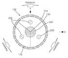
도 1은 본 발명의 제1 실시예에 따른 고 이득 광대역 안테나 장치의 구조를 도시한 도면이다.
도 2는 본 발명의 제1 실시예에 따른 고 이득 광대역 안테나 장치의 덮개부의 측면도이다.
도 3은 본 발명의 제1 실시예에 따른 고 이득 광대역 안테나 장치의 덮개부 양면의 도체 패턴을 구성하는 단위 셀의 예시도이다.
도 4는 본 발명의 제1 실시예에 따른 고 이득 광대역 안테나 장치의 덮개부 양면의 도체 패턴을 균일(uniform)하게 배열한 예시도이다.
도 5는 본 발명의 제1 실시예에 따른 고 이득 광대역 안테나 장치의 덮개부 양면의 도체 패턴을 불균일(non-uniform)하게 배열한 예시도이다.
도 6은 본 발명의 제1 실시예에 따른 고 이득 광대역 안테나 장치의 덮개부 양면의 도체 패턴을 구성하는 단위 셀의 다양한 예시도이다.
도 7은 본 발명의 제1 실시예에 따른 고 이득 광대역 안테나 장치의 덮개부에 평면파를 입사시켰을 때의 반사 특성을 도시한 그래프이다.
도 8은 본 발명의 제2 실시예에 따른 고 이득 광대역 안테나 장치의 구조를 도시한 도면이다.
도 9는 본 발명의 제3 실시예에 따른 고 이득 광대역 안테나 장치의 구조를 도시한 도면이다.
도 10은 도 9와 같이 금속벽면을 설치한 경우 안테나 이득의 변화를 도시한 그래프이다.
도 11은 도 9와 같이 금속벽면을 설치한 경우 안테나 전후방비의 변화를 도시한 그래프이다.
도 12는 본 발명의 제4 실시예에 따른 고 이득 광대역 안테나 장치의 구조를 도시한 도면이다.
도 13은 본 발명의 제5 실시예에 따른 고 이득 광대역 안테나 장치의 구조를 도시한 도면이다.1 is a diagram illustrating the structure of a high gain broadband antenna device according to a first embodiment of the present invention.
2 is a side view of a cover of the high gain broadband antenna device according to the first embodiment of the present invention.
3 is an exemplary diagram of a unit cell constituting a conductive pattern on both sides of a cover part of the high gain broadband antenna device according to the first embodiment of the present invention.
4 is an exemplary diagram in which conductor patterns on both sides of a cover part of the high gain broadband antenna device according to the first embodiment of the present invention are uniformly arranged.
FIG. 5 is an exemplary view of non-uniform arrangement of conductor patterns on both sides of a cover of a high gain broadband antenna device according to a first embodiment of the present invention.
FIG. 6 is a diagram illustrating various unit cells constituting a conductive pattern on both sides of a cover of the high gain wideband antenna device according to the first embodiment of the present invention.
7 is a graph showing reflection characteristics when a plane wave is incident on a cover portion of the high gain broadband antenna device according to the first embodiment of the present invention.
8 is a diagram illustrating the structure of a high gain wideband antenna device according to a second embodiment of the present invention.
9 is a diagram illustrating the structure of a high gain wideband antenna device according to a third embodiment of the present invention.
FIG. 10 is a graph illustrating a change in antenna gain when a metal wall surface is provided as shown in FIG. 9.
FIG. 11 is a graph illustrating changes in antenna front and rear ratios when a metal wall surface is installed as shown in FIG. 9.
12 is a diagram showing the structure of a high gain wideband antenna device according to a fourth embodiment of the present invention.
13 is a diagram showing the structure of a high gain wideband antenna device according to a fifth embodiment of the present invention.
이하에서는 본 발명에 따른 고 이득 광대역 안테나 장치를 첨부된 도면들을 참조하여 상세하게 설명한다. 이러한 과정에서 도면에 도시된 선들의 두께나 구성요소의 크기 등은 설명의 명료성과 편의상 과장되게 도시되어 있을 수 있다. 또한 후술되는 용어들은 본 발명에서의 기능을 고려하여 정의된 용어들로써, 이는 사용자, 운용자의 의도 또는 관례에 따라 달라질 수 있다. 그러므로 이러한 용어들에 대한 정의는 본 명세서 전반에 걸친 내용을 토대로 내려져야할 것이다.Hereinafter, a high gain broadband antenna device according to the present invention will be described in detail with reference to the accompanying drawings. In this process, the thicknesses of the lines and the sizes of the components shown in the drawings may be exaggerated for clarity and convenience of explanation. In addition, terms to be described later are terms defined in consideration of functions in the present invention, which may vary according to the intention or convention of a user or an operator. Therefore, the definitions of these terms should be made based on the contents throughout the specification.
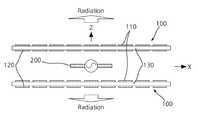
도 1은 본 발명의 제1 실시예에 따른 고 이득 광대역 안테나 장치의 구조를 도시한 도면이다.1 is a diagram illustrating the structure of a high gain broadband antenna device according to a first embodiment of the present invention.
도 1에 도시된 바와 같이, 본 발명의 제1 실시예에 따른 고 이득 광대역 안테나 장치는 덮개부(100), 급전 안테나(200) 및 접지면(300)을 포함한다.As shown in FIG. 1, the high gain broadband antenna device according to the first embodiment of the present invention includes a
이때, 본 발명에 따른 고 이득 광대역 안테나 장치는 안테나의 전후방비(FBR; Front Back Ratio)를 개선하기 위해 신호의 방사 방향을 기준으로 급전 안테나(200)의 측면에 배치되는 금속벽면(400)을 더 포함할 수 있다.In this case, the high gain wideband antenna device according to the present invention has a
도 2는 본 발명의 제1 실시예에 따른 고 이득 광대역 안테나 장치의 덮개부의 측면도이고, 도 3은 본 발명의 제1 실시예에 따른 고 이득 광대역 안테나 장치의 덮개부 양면의 도체 패턴을 구성하는 단위 셀의 예시도이다.FIG. 2 is a side view of a cover of the high gain broadband antenna device according to the first embodiment of the present invention, and FIG. 3 is a view illustrating a conductive pattern on both sides of the cover of the high gain broadband antenna device according to the first embodiment of the present invention. It is an illustration of a unit cell.
또한, 도 4는 본 발명의 제1 실시예에 따른 고 이득 광대역 안테나 장치의 덮개부 양면의 도체 패턴을 균일(uniform)하게 배열한 예시도이며, 도 5는 본 발명의 제1 실시예에 따른 고 이득 광대역 안테나 장치의 덮개부 양면의 도체 패턴을 불균일(non-uniform)하게 배열한 예시도이다.FIG. 4 is an exemplary view in which conductor patterns on both sides of a cover part of the high gain broadband antenna device according to the first embodiment of the present invention are uniformly arranged, and FIG. 5 is a view of the first embodiment of the present invention. It is an exemplary figure which non-uniformly arranged the conductor pattern of the both surfaces of the cover part of a high gain broadband antenna device.
추가적으로, 도 6은 본 발명의 제1 실시예에 따른 고 이득 광대역 안테나 장치의 덮개부 양면의 도체 패턴을 구성하는 단위 셀의 다양한 예시도이다.In addition, FIG. 6 is a diagram illustrating various unit cells constituting a conductive pattern on both sides of a cover of the high gain wideband antenna device according to the first embodiment of the present invention.
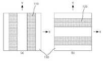
덮개부(100)는 도 2에 도시된 바와 같이, 일반적인 유전체 물질로 이루어진 유전체 기판(130) 및 유전체 기판(130)의 상,하부면에 형성되는 도체 패턴(110, 120)을 포함한다.As illustrated in FIG. 2, the
이때, 도체 패턴(110, 120)은 유전체 기판(130)의 상부면에 형성되는 상부 도체 패턴(110) 및 유전체 기판(130)의 하부면에 형성되는 하부 도체 패턴(120)을 포함한다.In this case, the
이러한 도체 패턴(110, 120)는 미리 설정된 특정 모양의 단위 셀이 x,y 축 방향으로 반복적으로 배열되어 형성될 수 있으며, 상부 도체 패턴(110)과 하부 도체 패턴(120)은 서로 상이한 모양으로 형성될 수 있다.The
구체적으로, 상부 도체 패턴(110)은 도 3의 (a)에 도시된 모양의 단위 셀이 x,y 축 방향으로 반복적으로 배열되어 형성될 수 있고, 하부 도체 패턴(120)은 도 3의 (b)에 도시된 모양의 단위 셀이 x,y 축 방향으로 반복적으로 배열되어 형성될 수 있다.Specifically, the
이때, 도 4에 도시된 바와 같이, 상부 도체 패턴(110) 및 하부 도체 패턴(120)은 각각을 구성하는 단위 셀의 크기를 동일하게 하여 균일(uniform)하게 형성될 수 있다.In this case, as shown in FIG. 4, the
반면, 도 5에 도시된 바와 같이, 상부 도체 패턴(110) 및 하부 도체 패턴(120)은 각각 상이한 크기의 단위 셀을 이용하여 불균일(non-uniform)하게 형성될 수도 있다.On the other hand, as shown in FIG. 5, the
이처럼 덮개부(100)의 도체 패턴(110, 120)이 불균일하게 형성되는 경우, 균일하게 형성되는 경우에 비해 광대역 측면에서 우수한 성능을 보이게 되며, 이러한 효과는 후술할 도 10에서 확인할 수 있다.As such, when the
한편, 도 2 내지 도 5에서는 도체 패턴(110, 120)을 구성하는 단위 셀의 모양이 x축 또는 y축 방향의 직사각형 패치 모양인 경우를 예로 들어 설명하였으나, 단위 셀의 모양이나 크기는 설계자의 의도와 시스템 사양 또는 발생시키고자 하는 반사 계수의 크기나 위상 등의 값에 따라 다양하게 선택될 수 있다.Meanwhile, in FIGS. 2 to 5, the shape of the unit cells constituting the
예를 들어, 덮개부(100)의 도체 패턴(110,120)을 구성하는 단위 셀은 도 6에 도시된 바와 같이 다양한 모양으로 구현되어, 반사 계수의 크기 및 위상 또는 대역폭 특성을 적절히 조절할 수 있다.For example, the unit cells constituting the
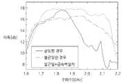
도 7은 본 발명의 제1 실시예에 따른 고 이득 광대역 안테나 장치의 덮개부에 평면파를 입사시켰을 때의 반사 특성을 도시한 그래프이다.7 is a graph showing reflection characteristics when a plane wave is incident on a cover portion of the high gain broadband antenna device according to the first embodiment of the present invention.
도 7을 참조하면, 반사 계수의 위상 기울기가 전 주파수 대역에서 음수의 값을 가지다가 동작 주파수 근방에서 양수의 값을 가짐을 확인할 수 있다.Referring to FIG. 7, it can be seen that the phase slope of the reflection coefficient has a negative value in all frequency bands and has a positive value near the operating frequency.
이는 광대역 공진 조건을 만족하는 이상적인 위상의 특성이 양수의 기울기를 가지는 경우와 일치하지만, 반사 계수의 값은 1 이하의 값을 가지므로, 패브리-페롯(Fabry-Perot) 공진기 안테나에 적용하는 경우 반사계수가 1인 경우보다 이득은 다소 작지만 비교적 높은 이득과 함께 광대역 특성을 제공할 수 있음을 확인할 수 있다.This coincides with the case where the ideal phase characteristic satisfying the broadband resonance condition has a positive slope, but the reflection coefficient has a value of 1 or less, so that the reflection when applied to a Fabry-Perot resonator antenna Although the gain is somewhat smaller than the coefficient of 1, it can be seen that it can provide broadband characteristics with a relatively high gain.
한편, 본 실시예에서 덮개부(100)의 유전체 기판(130) 상,하부면에 형성된 두 도체 패턴(110, 111) 사이의 거리는 파장의 약 1/100 정도 두께로 설정된다. 하지만, 이러한 유전체 기판(130)의 두께는 광대역화 하고자 하는 목표 주파수 대역의 너비나 목표로 하는 반사 계수의 크기 및 위상에 따라 더 두껍거나 더 얇게 구현될 수 있다.Meanwhile, in this embodiment, the distance between the two
즉, 유전체 기판(130)의 상,하부면에 형성되는 도체 패턴(110, 120)의 모양이나 크기뿐만 아니라, 유전체 기판(130)의 두께를 적절히 선택하여 반사 계수의 크기 및 위상, 대역폭 특성 이러한 특성이 나타나는 주파수 등을 조절할 수 있다.That is, not only the shape and size of the
또한, 유전체 기판(130)의 유전율을 적절히 선택함으로써, 반사 계수의 크기 및 위상, 대역폭 특성 이러한 특성이 나타나는 주파수 등을 조절할 수도 있다.In addition, by appropriately selecting the dielectric constant of the
급전 안테나(200)는 신호를 방사하는 안테나로, 신호를 급전할 수 있는 패치 안테나, 다이폴 안테나, 슬롯 안테나 또는 도파관 안테나 등 다양한 형태의 안테나를 포함할 수 있다.The
이때, 앞에서 설명한 덮개부(100)는 급전 안테나(200)에서 방사되는 신호의 방사 방향을 기준으로 덮개부(100)의 전면에 배치되며, 급전 안테나(200)에서 방사되는 신호는 덮개부(100)의 도체 패턴(110,120)을 향해 방사된다.At this time, the
접지면(300)은 급전 안테나(200)에서 방사되는 신호의 방사 방향을 기준으로 급전 안테나(200)의 후면에 배치되어 급전 안테나(200)를 접지시킨다.
The
도 8은 본 발명의 제2 실시예에 따른 고 이득 광대역 안테나 장치의 구조를 도시한 도면이다.8 is a diagram illustrating the structure of a high gain wideband antenna device according to a second embodiment of the present invention.
앞에서 설명한 제1 실시예에서는 고 이득 광대역 안테나 장치가 신호의 방사방향을 기준으로 급전 안테나(200)의 후면에 접지면(300)을 포함하는 경우를 예로 들어 설명하였다.In the first embodiment described above, the case where the high gain broadband antenna device includes the
하지만, 본 발명에 따른 고 이득 광대역 안테나 장치는 도 8에 도시된 바와 같이, 접지면(300) 대신에 덮개부(100)를 하나 더 포함하도록 구현될 수도 있다.However, the high gain broadband antenna device according to the present invention may be implemented to include one
즉, 본 발명에 따른 고 이득 광대역 안테나 장치는 유전체 기판(130)의 상,하부면에 형성된 도체 패턴(110,120)을 구비하는 복수 개의 덮개부(100) 및 복수 개의 덮개부(100) 사이에 배치되어 복수 개의 덮개부(100)에 구비된 복수 개의 도체 패턴(110,120)으로 신호를 방사하는 급전 안테나(200)를 포함할 수 있다.That is, the high gain broadband antenna device according to the present invention is disposed between the plurality of
이와 같이 구성하는 경우 안테나의 이득과 대역폭을 보다 증대시킬 수 있는 이점이 있다.
In such a configuration, there is an advantage in that the gain and bandwidth of the antenna can be further increased.
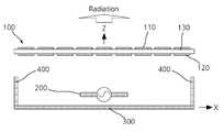
도 9는 본 발명의 제3 실시예에 따른 고 이득 광대역 안테나 장치의 구조를 도시한 도면이고, 도 10은 도 9와 같이 금속벽면을 설치한 경우 안테나 이득의 변화를 도시한 그래프이며, 도 11은 도 9와 같이 금속벽면을 설치한 경우 안테나 전후방비의 변화를 도시한 그래프이다.FIG. 9 is a diagram illustrating a structure of a high gain broadband antenna device according to a third embodiment of the present invention. FIG. 10 is a graph illustrating a change in antenna gain when a metal wall surface is installed as shown in FIG. 9 is a graph showing the change of the antenna front and rear ratio when the metal wall surface is installed as shown in FIG.
앞에서 설명한 제1,2 실시예와 달리, 본 발명에 따른 고 이득 광대역 안테나 장치는 도 9에 도시된 바와 같이 신호의 방사 방향을 기준으로 급전 안테나(200)의 측면에 배치되는 금속벽면(400)을 더 포함할 수 있다.Unlike the first and second embodiments described above, the high gain broadband antenna device according to the present invention has a
도 10을 참조하면, 덮개부(100)의 도체 패턴(110, 120)을 균일하게 배열한 경우에 비해 불균일하게 배열한 경우에 광대역 특성이 개선됨을 확인할 수 있으며, 금속벽면(400)을 설치한 경우에 안테나의 이득이 향상되는 것을 확인할 수 있다.Referring to FIG. 10, it can be seen that the broadband characteristics are improved when the
또한, 도 11을 참조하면, 금속벽면(400)이 배치되는 경우에 안테나의 전후방비가 개선되는 것을 확인할 수 있다.In addition, referring to FIG. 11, it can be seen that the front and rear ratio of the antenna is improved when the
즉, 급전 안테나(200)의 좌우측면에 금속벽면(400)을 설치함으로써 안테나의 이득 및 전후방비를 개선할 수 있다.That is, by providing the
도 12는 본 발명의 제4 실시예에 따른 고 이득 광대역 안테나 장치의 구조를 도시한 도면이고, 도 13은 본 발명의 제5 실시예에 따른 고 이득 광대역 안테나 장치의 구조를 도시한 도면이다.12 is a diagram showing the structure of a high gain wideband antenna device according to a fourth embodiment of the present invention, and FIG. 13 is a diagram showing the structure of a high gain wideband antenna device according to a fifth embodiment of the present invention.
앞에서 설명한 제1,2,3 실시예에서는 덮개부(100)가 평면형으로 구현되는 경우를 예로 들어 설명하였으나, 이와 달리 덮개부(100)는 원통형으로 구현될 수도 있다.In the above-described first, second, and third embodiments, the case in which the
즉, 도 12에 도시된 바와 같이, 본 발명에 따른 고 이득 광대역 안테나 장치는 원통형의 유전체 기판(130)의 내,외부면에 형성되는 도체 패턴(110,120)을 구비하는 덮개부(100)와 덮개부(100)의 내부에 배치되어 덮개부(100)에 구비된 도체 패턴(110,120)으로 신호를 방사하는 하나의 급전 안테나(200)를 포함할 수 있다.That is, as shown in FIG. 12, the high gain broadband antenna device according to the present invention includes a
또는, 도 13에 도시된 바와 같이, 본 발명에 따른 고 이득 광대역 장치는 원통형의 유전체 기판(130)의 내,외부면에 형성되는 도체 패턴(110,120)을 구비하는 덮개부(100)와 덮개부(100) 내부에 구획된 복수 개의 영역 내에 각각 배치되는 복수 개의 급전 안테나(200) 및 복수 개의 영역에 공통되는 중심 영역에 위치하여 급전 안테나(200)를 접지시키는 접지면(300)을 포함하여 섹터 형태의 안테나로 구현될 수도 있다.Alternatively, as shown in FIG. 13, the high gain broadband device according to the present invention includes a
또한, 이와 달리 덮개부(100)를 구형(공 모양)으로 구현하여 안테나 장치에 적용할 수도 있다 할 것이다.
Alternatively, the
이와 같이, 본 발명에 따른 고 이득 광대역 장치에 따르면, 패브리-페롯(Fabry-Perot) 공진기를 이용한 안테나에서 유전체 물질의 양면에 도체 패턴들을 적절히 구성하여 특정 주파수 대역에서의 반사 계수의 위상을 조절함으로써, 안테나의 이득과 대역폭을 증대시킬 수 있다.As described above, according to the high gain broadband device according to the present invention, in the antenna using a Fabry-Perot resonator, by appropriately configuring the conductor patterns on both sides of the dielectric material to adjust the phase of the reflection coefficient in a specific frequency band As a result, the gain and bandwidth of the antenna can be increased.
또한, 도체 패턴(110,120)의 크기를 불균일하게 구성하여 안테나의 대역폭을 보다 확장시킬 수 있으며, 급전 안테나(200)의 측면에 금속벽면(400)을 추가로 배치함으로써 안테나의 전후방비를 보다 개선할 수 있다.In addition, by unevenly configuring the size of the
본 발명은 도면에 도시된 실시예를 참고로 하여 설명되었으나, 이는 예시적인 것에 불과하며 당해 기술이 속하는 기술분야에서 통상의 지식을 가진 자라면 이로부터 다양한 변형 및 균등한 타 실시예가 가능하다는 점을 이해할 것이다. 따라서, 본 발명의 진정한 기술적 보호범위는 아래의 특허청구범위에 의하여 정해져야할 것이다.
While the present invention has been particularly shown and described with reference to exemplary embodiments thereof, it is clearly understood that the same is by way of illustration and example only and is not to be taken by way of limitation, I will understand. Accordingly, the true scope of the present invention should be determined by the following claims.
100 : 덮개부
110 : 상부 도체 패턴
120 : 하부 도체 패턴
200 : 급전 안테나
300 : 접지면
400 : 금속벽면100:
110: upper conductor pattern
120: lower conductor pattern
200: feed antenna
300: ground plane
400: metal wall surface
Claims (18)
Translated fromKorean상기 신호의 방사 방향을 기준으로 상기 급전 안테나의 전면에 배치되며, 특정 모양으로 형성되는 도체 패턴을 구비하는 덮개부; 및
상기 신호의 방사 방향을 기준으로 상기 급전 안테나의 후면에 배치되는 접지면을 포함하는 고 이득 광대역 안테나 장치.
A feed antenna for emitting a signal;
A cover part disposed on a front surface of the feed antenna based on a radiation direction of the signal and having a conductor pattern formed in a specific shape; And
And a ground plane disposed on a rear surface of the feed antenna based on the radiation direction of the signal.
상기 도체 패턴은 상기 덮개부를 구성하는 유전체 기판의 상,하부면에 각각 서로 다른 모양으로 형성되는 것을 특징으로 하는 고 이득 광대역 안테나 장치.
The method of claim 1,
The conductor pattern may be formed in different shapes on the upper and lower surfaces of the dielectric substrate constituting the cover.
상기 도체 패턴은 미리 설정된 단위 셀이 반복적으로 배열되어 형성되는 것을 특징으로 하는 고 이득 광대역 안테나 장치.
The method of claim 1,
The conductor pattern is a high gain wideband antenna device, characterized in that formed in a predetermined unit cells are arranged repeatedly.
상기 도체 패턴은 상기 단위 셀의 크기가 불균일하게 배열되어 형성되는 것을 특징으로 하는 고 이득 광대역 안테나 장치.
The method of claim 3, wherein
The conductor pattern is a high gain broadband antenna device, characterized in that formed in the unit cell size is unevenly arranged.
상기 신호의 방사 방향을 기준으로 상기 급전 안테나의 측면에 배치되는 금속벽면을 더 포함하는 것을 특징으로 하는 고 이득 광대역 안테나 장치.
The method of claim 1,
And a metal wall surface disposed on a side of the feed antenna based on the radiation direction of the signal.
상기 신호의 방사 방향을 기준으로 상기 급전 안테나의 전,후면에 각각 배치되며, 특정 모양으로 형성되는 도체 패턴을 각각 구비하는 덮개부를 포함하는 고 이득 광대역 안테나 장치.
A feed antenna for emitting a signal; And
And a cover part disposed on each of the front and rear surfaces of the feed antenna based on the radiation direction of the signal, the cover part having a conductor pattern each having a specific shape.
상기 도체 패턴은 상기 덮개부를 구성하는 유전체 기판의 상,하부면에 각각 서로 다른 모양으로 형성되는 것을 특징으로 하는 고 이득 광대역 안테나 장치
The method according to claim 6,
The conductive pattern is formed on the upper and lower surfaces of the dielectric substrate constituting the cover portion, respectively, characterized in that the high gain broadband antenna device
상기 도체 패턴은 미리 설정된 단위 셀이 반복적으로 배열되어 형성되는 것을 특징으로 하는 고 이득 광대역 안테나 장치.
The method according to claim 6,
The conductor pattern is a high gain wideband antenna device, characterized in that formed in a predetermined unit cells are arranged repeatedly.
상기 도체 패턴은 상기 단위 셀의 크기가 불균일하게 배열되어 형성되는 것을 특징으로 하는 고 이득 광대역 안테나 장치.
The method of claim 8,
The conductor pattern is a high gain broadband antenna device, characterized in that formed in the unit cell size is unevenly arranged.
상기 신호의 방사 방향을 기준으로 상기 급전 안테나의 측면에 배치되는 금속벽면을 더 포함하는 것을 특징으로 하는 고 이득 광대역 안테나 장치.
The method according to claim 6,
And a metal wall surface disposed on a side of the feed antenna based on the radiation direction of the signal.
상기 덮개부의 내부에 배치되어 상기 도체 패턴으로 신호를 방사하는 급전 안테나를 포함하는 고 이득 광대역 안테나 장치.
A cylindrical cover part having a conductor pattern formed in a specific shape; And
And a feed antenna disposed in the cover part to emit a signal in the conductor pattern.
상기 도체 패턴은 상기 덮개부를 구성하는 원통형의 유전체 기판의 내,외부면에 각각 서로 다른 모양으로 형성되는 것을 특징으로 하는 고 이득 광대역 안테나 장치.
12. The method of claim 11,
The conductor pattern is a high gain broadband antenna device, characterized in that formed on the inner and outer surfaces of the cylindrical dielectric substrate constituting the cover portion respectively different.
상기 도체 패턴은 미리 설정된 단위 셀이 반복적으로 배열되어 형성되는 것을 특징으로 하는 고 이득 광대역 안테나 장치.
12. The method of claim 11,
The conductor pattern is a high gain wideband antenna device, characterized in that formed in a predetermined unit cells are arranged repeatedly.
상기 도체 패턴은 상기 단위 셀의 크기가 불균일하게 배열되어 형성되는 것을 특징으로 하는 고 이득 광대역 안테나 장치.
The method of claim 13,
The conductor pattern is a high gain broadband antenna device, characterized in that formed in the unit cell size is unevenly arranged.
상기 덮개부 내부에 구획된 복수 개의 영역 내에 각각 배치되어 상기 도체 패턴으로 신호를 방사하는 복수 개의 급전 안테나; 및
상기 복수 개의 영역에 공통되는 중심 영역에 위치하는 접지면을 포함하는 고 이득 광대역 안테나 장치.
A cylindrical cover part having a conductor pattern formed in a specific shape;
A plurality of feed antennas disposed in a plurality of areas partitioned inside the cover part to emit signals in the conductor pattern; And
And a ground plane positioned in a central region common to the plurality of regions.
상기 도체 패턴은 상기 덮개부를 구성하는 원통형의 유전체 기판의 내,외부면에 각각 서로 다른 모양으로 형성되는 것을 특징으로 하는 고 이득 광대역 안테나 장치.
16. The method of claim 15,
The conductor pattern is a high gain broadband antenna device, characterized in that formed on the inner and outer surfaces of the cylindrical dielectric substrate constituting the cover portion respectively different.
상기 도체 패턴은 미리 설정된 단위 셀이 반복적으로 배열되어 형성되는 것을 특징으로 하는 고 이득 광대역 안테나 장치.
16. The method of claim 15,
The conductor pattern is a high gain wideband antenna device, characterized in that formed in a predetermined unit cells are arranged repeatedly.
상기 도체 패턴은 상기 단위 셀의 크기가 불균일하게 배열되어 형성되는 것을 특징으로 하는 고 이득 광대역 안테나 장치.
18. The method of claim 17,
The conductor pattern is a high gain broadband antenna device, characterized in that formed in the unit cell size is unevenly arranged.
Priority Applications (2)
| Application Number | Priority Date | Filing Date | Title |
|---|---|---|---|
| KR1020120019956AKR20130098098A (en) | 2012-02-27 | 2012-02-27 | High-gain wideband antenna apparatus |
| US13/746,384US9246231B2 (en) | 2012-02-27 | 2013-01-22 | High-gain wideband antenna apparatus |
Applications Claiming Priority (1)
| Application Number | Priority Date | Filing Date | Title |
|---|---|---|---|
| KR1020120019956AKR20130098098A (en) | 2012-02-27 | 2012-02-27 | High-gain wideband antenna apparatus |
Publications (1)
| Publication Number | Publication Date |
|---|---|
| KR20130098098Atrue KR20130098098A (en) | 2013-09-04 |
Family
ID=49002254
Family Applications (1)
| Application Number | Title | Priority Date | Filing Date |
|---|---|---|---|
| KR1020120019956AWithdrawnKR20130098098A (en) | 2012-02-27 | 2012-02-27 | High-gain wideband antenna apparatus |
Country Status (2)
| Country | Link |
|---|---|
| US (1) | US9246231B2 (en) |
| KR (1) | KR20130098098A (en) |
Cited By (8)
| Publication number | Priority date | Publication date | Assignee | Title |
|---|---|---|---|---|
| KR101709074B1 (en)* | 2015-11-13 | 2017-02-23 | 현대자동차주식회사 | Antenna and vehicle having the same |
| WO2017043946A1 (en)* | 2015-09-11 | 2017-03-16 | 세종대학교산학협력단 | Reflective cell-array antenna having miniaturised structure |
| WO2018199549A1 (en)* | 2017-04-25 | 2018-11-01 | 삼성전자 주식회사 | Metamaterial structure antenna and metamaterial structure array |
| US10199746B2 (en) | 2015-10-15 | 2019-02-05 | Hyundai Motor Company | Antenna apparatus, vehicle having the antenna apparatus, and method for controlling the antenna apparatus |
| KR20200018945A (en)* | 2018-08-13 | 2020-02-21 | 삼성전자주식회사 | Antenna device including planar lens |
| KR20210044729A (en) | 2019-10-15 | 2021-04-23 | 서울대학교산학협력단 | Liquid crystal based frequency reconfigurable prs antenna system |
| CN113285237A (en)* | 2021-05-18 | 2021-08-20 | 重庆邮电大学 | Broadband high-gain Fabry-Perot resonant cavity antenna |
| KR102299534B1 (en)* | 2020-03-25 | 2021-09-08 | 인천대학교 산학협력단 | A Small RFID Antenna System with Plenar Reflectarray for High Antenna Gain |
Families Citing this family (164)
| Publication number | Priority date | Publication date | Assignee | Title |
|---|---|---|---|---|
| US9113347B2 (en) | 2012-12-05 | 2015-08-18 | At&T Intellectual Property I, Lp | Backhaul link for distributed antenna system |
| US9525524B2 (en) | 2013-05-31 | 2016-12-20 | At&T Intellectual Property I, L.P. | Remote distributed antenna system |
| US9999038B2 (en) | 2013-05-31 | 2018-06-12 | At&T Intellectual Property I, L.P. | Remote distributed antenna system |
| US8897697B1 (en) | 2013-11-06 | 2014-11-25 | At&T Intellectual Property I, Lp | Millimeter-wave surface-wave communications |
| US9768833B2 (en) | 2014-09-15 | 2017-09-19 | At&T Intellectual Property I, L.P. | Method and apparatus for sensing a condition in a transmission medium of electromagnetic waves |
| US10063280B2 (en) | 2014-09-17 | 2018-08-28 | At&T Intellectual Property I, L.P. | Monitoring and mitigating conditions in a communication network |
| US9615269B2 (en) | 2014-10-02 | 2017-04-04 | At&T Intellectual Property I, L.P. | Method and apparatus that provides fault tolerance in a communication network |
| US9685992B2 (en) | 2014-10-03 | 2017-06-20 | At&T Intellectual Property I, L.P. | Circuit panel network and methods thereof |
| US9503189B2 (en) | 2014-10-10 | 2016-11-22 | At&T Intellectual Property I, L.P. | Method and apparatus for arranging communication sessions in a communication system |
| US9973299B2 (en) | 2014-10-14 | 2018-05-15 | At&T Intellectual Property I, L.P. | Method and apparatus for adjusting a mode of communication in a communication network |
| US9762289B2 (en) | 2014-10-14 | 2017-09-12 | At&T Intellectual Property I, L.P. | Method and apparatus for transmitting or receiving signals in a transportation system |
| US9653770B2 (en) | 2014-10-21 | 2017-05-16 | At&T Intellectual Property I, L.P. | Guided wave coupler, coupling module and methods for use therewith |
| US9520945B2 (en) | 2014-10-21 | 2016-12-13 | At&T Intellectual Property I, L.P. | Apparatus for providing communication services and methods thereof |
| US9577306B2 (en) | 2014-10-21 | 2017-02-21 | At&T Intellectual Property I, L.P. | Guided-wave transmission device and methods for use therewith |
| US9780834B2 (en) | 2014-10-21 | 2017-10-03 | At&T Intellectual Property I, L.P. | Method and apparatus for transmitting electromagnetic waves |
| US9312919B1 (en) | 2014-10-21 | 2016-04-12 | At&T Intellectual Property I, Lp | Transmission device with impairment compensation and methods for use therewith |
| US9769020B2 (en) | 2014-10-21 | 2017-09-19 | At&T Intellectual Property I, L.P. | Method and apparatus for responding to events affecting communications in a communication network |
| US9627768B2 (en) | 2014-10-21 | 2017-04-18 | At&T Intellectual Property I, L.P. | Guided-wave transmission device with non-fundamental mode propagation and methods for use therewith |
| US9461706B1 (en) | 2015-07-31 | 2016-10-04 | At&T Intellectual Property I, Lp | Method and apparatus for exchanging communication signals |
| US9997819B2 (en) | 2015-06-09 | 2018-06-12 | At&T Intellectual Property I, L.P. | Transmission medium and method for facilitating propagation of electromagnetic waves via a core |
| US9544006B2 (en) | 2014-11-20 | 2017-01-10 | At&T Intellectual Property I, L.P. | Transmission device with mode division multiplexing and methods for use therewith |
| US10243784B2 (en) | 2014-11-20 | 2019-03-26 | At&T Intellectual Property I, L.P. | System for generating topology information and methods thereof |
| US9800327B2 (en) | 2014-11-20 | 2017-10-24 | At&T Intellectual Property I, L.P. | Apparatus for controlling operations of a communication device and methods thereof |
| US9954287B2 (en) | 2014-11-20 | 2018-04-24 | At&T Intellectual Property I, L.P. | Apparatus for converting wireless signals and electromagnetic waves and methods thereof |
| US10009067B2 (en) | 2014-12-04 | 2018-06-26 | At&T Intellectual Property I, L.P. | Method and apparatus for configuring a communication interface |
| KR102175681B1 (en)* | 2014-11-20 | 2020-11-06 | 삼성전자주식회사 | Reradiate repeater |
| US9742462B2 (en) | 2014-12-04 | 2017-08-22 | At&T Intellectual Property I, L.P. | Transmission medium and communication interfaces and methods for use therewith |
| US10340573B2 (en) | 2016-10-26 | 2019-07-02 | At&T Intellectual Property I, L.P. | Launcher with cylindrical coupling device and methods for use therewith |
| CN104466385A (en)* | 2014-11-27 | 2015-03-25 | 张永超 | Novel antenna housing with high wave transmittance |
| CN104466386A (en)* | 2014-11-27 | 2015-03-25 | 张永超 | Low-loss metamaterial antenna housing |
| US10144036B2 (en) | 2015-01-30 | 2018-12-04 | At&T Intellectual Property I, L.P. | Method and apparatus for mitigating interference affecting a propagation of electromagnetic waves guided by a transmission medium |
| US9876570B2 (en) | 2015-02-20 | 2018-01-23 | At&T Intellectual Property I, Lp | Guided-wave transmission device with non-fundamental mode propagation and methods for use therewith |
| US9749013B2 (en) | 2015-03-17 | 2017-08-29 | At&T Intellectual Property I, L.P. | Method and apparatus for reducing attenuation of electromagnetic waves guided by a transmission medium |
| US10224981B2 (en) | 2015-04-24 | 2019-03-05 | At&T Intellectual Property I, Lp | Passive electrical coupling device and methods for use therewith |
| US9705561B2 (en) | 2015-04-24 | 2017-07-11 | At&T Intellectual Property I, L.P. | Directional coupling device and methods for use therewith |
| US9793954B2 (en) | 2015-04-28 | 2017-10-17 | At&T Intellectual Property I, L.P. | Magnetic coupling device and methods for use therewith |
| US9948354B2 (en) | 2015-04-28 | 2018-04-17 | At&T Intellectual Property I, L.P. | Magnetic coupling device with reflective plate and methods for use therewith |
| US9871282B2 (en) | 2015-05-14 | 2018-01-16 | At&T Intellectual Property I, L.P. | At least one transmission medium having a dielectric surface that is covered at least in part by a second dielectric |
| US9748626B2 (en) | 2015-05-14 | 2017-08-29 | At&T Intellectual Property I, L.P. | Plurality of cables having different cross-sectional shapes which are bundled together to form a transmission medium |
| US9490869B1 (en) | 2015-05-14 | 2016-11-08 | At&T Intellectual Property I, L.P. | Transmission medium having multiple cores and methods for use therewith |
| US10650940B2 (en) | 2015-05-15 | 2020-05-12 | At&T Intellectual Property I, L.P. | Transmission medium having a conductive material and methods for use therewith |
| US9917341B2 (en) | 2015-05-27 | 2018-03-13 | At&T Intellectual Property I, L.P. | Apparatus and method for launching electromagnetic waves and for modifying radial dimensions of the propagating electromagnetic waves |
| US9866309B2 (en) | 2015-06-03 | 2018-01-09 | At&T Intellectual Property I, Lp | Host node device and methods for use therewith |
| US10812174B2 (en) | 2015-06-03 | 2020-10-20 | At&T Intellectual Property I, L.P. | Client node device and methods for use therewith |
| US9912381B2 (en) | 2015-06-03 | 2018-03-06 | At&T Intellectual Property I, Lp | Network termination and methods for use therewith |
| US10103801B2 (en) | 2015-06-03 | 2018-10-16 | At&T Intellectual Property I, L.P. | Host node device and methods for use therewith |
| US9913139B2 (en) | 2015-06-09 | 2018-03-06 | At&T Intellectual Property I, L.P. | Signal fingerprinting for authentication of communicating devices |
| US9608692B2 (en) | 2015-06-11 | 2017-03-28 | At&T Intellectual Property I, L.P. | Repeater and methods for use therewith |
| US9820146B2 (en) | 2015-06-12 | 2017-11-14 | At&T Intellectual Property I, L.P. | Method and apparatus for authentication and identity management of communicating devices |
| US9667317B2 (en) | 2015-06-15 | 2017-05-30 | At&T Intellectual Property I, L.P. | Method and apparatus for providing security using network traffic adjustments |
| US9509415B1 (en) | 2015-06-25 | 2016-11-29 | At&T Intellectual Property I, L.P. | Methods and apparatus for inducing a fundamental wave mode on a transmission medium |
| US9865911B2 (en) | 2015-06-25 | 2018-01-09 | At&T Intellectual Property I, L.P. | Waveguide system for slot radiating first electromagnetic waves that are combined into a non-fundamental wave mode second electromagnetic wave on a transmission medium |
| US9640850B2 (en) | 2015-06-25 | 2017-05-02 | At&T Intellectual Property I, L.P. | Methods and apparatus for inducing a non-fundamental wave mode on a transmission medium |
| CN105006642A (en)* | 2015-06-26 | 2015-10-28 | 桂林电子科技大学 | Single-negative material separating plate and broadband high-isolation monopole array antenna |
| US10044409B2 (en) | 2015-07-14 | 2018-08-07 | At&T Intellectual Property I, L.P. | Transmission medium and methods for use therewith |
| US9853342B2 (en) | 2015-07-14 | 2017-12-26 | At&T Intellectual Property I, L.P. | Dielectric transmission medium connector and methods for use therewith |
| US9882257B2 (en) | 2015-07-14 | 2018-01-30 | At&T Intellectual Property I, L.P. | Method and apparatus for launching a wave mode that mitigates interference |
| US10205655B2 (en) | 2015-07-14 | 2019-02-12 | At&T Intellectual Property I, L.P. | Apparatus and methods for communicating utilizing an antenna array and multiple communication paths |
| US9722318B2 (en) | 2015-07-14 | 2017-08-01 | At&T Intellectual Property I, L.P. | Method and apparatus for coupling an antenna to a device |
| US9847566B2 (en) | 2015-07-14 | 2017-12-19 | At&T Intellectual Property I, L.P. | Method and apparatus for adjusting a field of a signal to mitigate interference |
| US10148016B2 (en) | 2015-07-14 | 2018-12-04 | At&T Intellectual Property I, L.P. | Apparatus and methods for communicating utilizing an antenna array |
| US10033108B2 (en) | 2015-07-14 | 2018-07-24 | At&T Intellectual Property I, L.P. | Apparatus and methods for generating an electromagnetic wave having a wave mode that mitigates interference |
| US10320586B2 (en) | 2015-07-14 | 2019-06-11 | At&T Intellectual Property I, L.P. | Apparatus and methods for generating non-interfering electromagnetic waves on an insulated transmission medium |
| US9628116B2 (en) | 2015-07-14 | 2017-04-18 | At&T Intellectual Property I, L.P. | Apparatus and methods for transmitting wireless signals |
| US10170840B2 (en) | 2015-07-14 | 2019-01-01 | At&T Intellectual Property I, L.P. | Apparatus and methods for sending or receiving electromagnetic signals |
| US10341142B2 (en) | 2015-07-14 | 2019-07-02 | At&T Intellectual Property I, L.P. | Apparatus and methods for generating non-interfering electromagnetic waves on an uninsulated conductor |
| US10090606B2 (en) | 2015-07-15 | 2018-10-02 | At&T Intellectual Property I, L.P. | Antenna system with dielectric array and methods for use therewith |
| US9608740B2 (en) | 2015-07-15 | 2017-03-28 | At&T Intellectual Property I, L.P. | Method and apparatus for launching a wave mode that mitigates interference |
| US9793951B2 (en) | 2015-07-15 | 2017-10-17 | At&T Intellectual Property I, L.P. | Method and apparatus for launching a wave mode that mitigates interference |
| US9912027B2 (en) | 2015-07-23 | 2018-03-06 | At&T Intellectual Property I, L.P. | Method and apparatus for exchanging communication signals |
| US9749053B2 (en) | 2015-07-23 | 2017-08-29 | At&T Intellectual Property I, L.P. | Node device, repeater and methods for use therewith |
| US9948333B2 (en) | 2015-07-23 | 2018-04-17 | At&T Intellectual Property I, L.P. | Method and apparatus for wireless communications to mitigate interference |
| US9871283B2 (en) | 2015-07-23 | 2018-01-16 | At&T Intellectual Property I, Lp | Transmission medium having a dielectric core comprised of plural members connected by a ball and socket configuration |
| US9735833B2 (en) | 2015-07-31 | 2017-08-15 | At&T Intellectual Property I, L.P. | Method and apparatus for communications management in a neighborhood network |
| US9967173B2 (en) | 2015-07-31 | 2018-05-08 | At&T Intellectual Property I, L.P. | Method and apparatus for authentication and identity management of communicating devices |
| US9904535B2 (en) | 2015-09-14 | 2018-02-27 | At&T Intellectual Property I, L.P. | Method and apparatus for distributing software |
| US10079661B2 (en) | 2015-09-16 | 2018-09-18 | At&T Intellectual Property I, L.P. | Method and apparatus for use with a radio distributed antenna system having a clock reference |
| US10136434B2 (en) | 2015-09-16 | 2018-11-20 | At&T Intellectual Property I, L.P. | Method and apparatus for use with a radio distributed antenna system having an ultra-wideband control channel |
| US10009063B2 (en) | 2015-09-16 | 2018-06-26 | At&T Intellectual Property I, L.P. | Method and apparatus for use with a radio distributed antenna system having an out-of-band reference signal |
| US9769128B2 (en) | 2015-09-28 | 2017-09-19 | At&T Intellectual Property I, L.P. | Method and apparatus for encryption of communications over a network |
| US9729197B2 (en) | 2015-10-01 | 2017-08-08 | At&T Intellectual Property I, L.P. | Method and apparatus for communicating network management traffic over a network |
| US9876264B2 (en) | 2015-10-02 | 2018-01-23 | At&T Intellectual Property I, Lp | Communication system, guided wave switch and methods for use therewith |
| US10355367B2 (en) | 2015-10-16 | 2019-07-16 | At&T Intellectual Property I, L.P. | Antenna structure for exchanging wireless signals |
| US10270160B2 (en)* | 2016-04-27 | 2019-04-23 | Topcon Positioning Systems, Inc. | Antenna radomes forming a cut-off pattern |
| KR101803196B1 (en)* | 2016-06-28 | 2017-11-29 | 홍익대학교 산학협력단 | System for high gain antenna beam steering using parealectric |
| US9912419B1 (en) | 2016-08-24 | 2018-03-06 | At&T Intellectual Property I, L.P. | Method and apparatus for managing a fault in a distributed antenna system |
| US9860075B1 (en) | 2016-08-26 | 2018-01-02 | At&T Intellectual Property I, L.P. | Method and communication node for broadband distribution |
| US10218079B2 (en)* | 2016-08-29 | 2019-02-26 | Venti Group, LLC | Periodic array assembly comprising arrays of periodic elements having inwardly extending protrusions |
| US10291311B2 (en) | 2016-09-09 | 2019-05-14 | At&T Intellectual Property I, L.P. | Method and apparatus for mitigating a fault in a distributed antenna system |
| US11032819B2 (en) | 2016-09-15 | 2021-06-08 | At&T Intellectual Property I, L.P. | Method and apparatus for use with a radio distributed antenna system having a control channel reference signal |
| US10135146B2 (en) | 2016-10-18 | 2018-11-20 | At&T Intellectual Property I, L.P. | Apparatus and methods for launching guided waves via circuits |
| US10135147B2 (en) | 2016-10-18 | 2018-11-20 | At&T Intellectual Property I, L.P. | Apparatus and methods for launching guided waves via an antenna |
| US10340600B2 (en) | 2016-10-18 | 2019-07-02 | At&T Intellectual Property I, L.P. | Apparatus and methods for launching guided waves via plural waveguide systems |
| US9876605B1 (en) | 2016-10-21 | 2018-01-23 | At&T Intellectual Property I, L.P. | Launcher and coupling system to support desired guided wave mode |
| US9991580B2 (en) | 2016-10-21 | 2018-06-05 | At&T Intellectual Property I, L.P. | Launcher and coupling system for guided wave mode cancellation |
| US10374316B2 (en) | 2016-10-21 | 2019-08-06 | At&T Intellectual Property I, L.P. | System and dielectric antenna with non-uniform dielectric |
| US10811767B2 (en) | 2016-10-21 | 2020-10-20 | At&T Intellectual Property I, L.P. | System and dielectric antenna with convex dielectric radome |
| US10312567B2 (en) | 2016-10-26 | 2019-06-04 | At&T Intellectual Property I, L.P. | Launcher with planar strip antenna and methods for use therewith |
| US10291334B2 (en) | 2016-11-03 | 2019-05-14 | At&T Intellectual Property I, L.P. | System for detecting a fault in a communication system |
| US10224634B2 (en) | 2016-11-03 | 2019-03-05 | At&T Intellectual Property I, L.P. | Methods and apparatus for adjusting an operational characteristic of an antenna |
| US10498044B2 (en) | 2016-11-03 | 2019-12-03 | At&T Intellectual Property I, L.P. | Apparatus for configuring a surface of an antenna |
| US10225025B2 (en) | 2016-11-03 | 2019-03-05 | At&T Intellectual Property I, L.P. | Method and apparatus for detecting a fault in a communication system |
| US10340601B2 (en) | 2016-11-23 | 2019-07-02 | At&T Intellectual Property I, L.P. | Multi-antenna system and methods for use therewith |
| US10535928B2 (en) | 2016-11-23 | 2020-01-14 | At&T Intellectual Property I, L.P. | Antenna system and methods for use therewith |
| US10178445B2 (en) | 2016-11-23 | 2019-01-08 | At&T Intellectual Property I, L.P. | Methods, devices, and systems for load balancing between a plurality of waveguides |
| US10340603B2 (en) | 2016-11-23 | 2019-07-02 | At&T Intellectual Property I, L.P. | Antenna system having shielded structural configurations for assembly |
| US10090594B2 (en) | 2016-11-23 | 2018-10-02 | At&T Intellectual Property I, L.P. | Antenna system having structural configurations for assembly |
| US10305190B2 (en) | 2016-12-01 | 2019-05-28 | At&T Intellectual Property I, L.P. | Reflecting dielectric antenna system and methods for use therewith |
| US10361489B2 (en) | 2016-12-01 | 2019-07-23 | At&T Intellectual Property I, L.P. | Dielectric dish antenna system and methods for use therewith |
| US10637149B2 (en) | 2016-12-06 | 2020-04-28 | At&T Intellectual Property I, L.P. | Injection molded dielectric antenna and methods for use therewith |
| US10727599B2 (en) | 2016-12-06 | 2020-07-28 | At&T Intellectual Property I, L.P. | Launcher with slot antenna and methods for use therewith |
| US9927517B1 (en) | 2016-12-06 | 2018-03-27 | At&T Intellectual Property I, L.P. | Apparatus and methods for sensing rainfall |
| US10439675B2 (en) | 2016-12-06 | 2019-10-08 | At&T Intellectual Property I, L.P. | Method and apparatus for repeating guided wave communication signals |
| US10694379B2 (en) | 2016-12-06 | 2020-06-23 | At&T Intellectual Property I, L.P. | Waveguide system with device-based authentication and methods for use therewith |
| US10819035B2 (en) | 2016-12-06 | 2020-10-27 | At&T Intellectual Property I, L.P. | Launcher with helical antenna and methods for use therewith |
| US10755542B2 (en) | 2016-12-06 | 2020-08-25 | At&T Intellectual Property I, L.P. | Method and apparatus for surveillance via guided wave communication |
| US10020844B2 (en) | 2016-12-06 | 2018-07-10 | T&T Intellectual Property I, L.P. | Method and apparatus for broadcast communication via guided waves |
| US10135145B2 (en) | 2016-12-06 | 2018-11-20 | At&T Intellectual Property I, L.P. | Apparatus and methods for generating an electromagnetic wave along a transmission medium |
| US10382976B2 (en) | 2016-12-06 | 2019-08-13 | At&T Intellectual Property I, L.P. | Method and apparatus for managing wireless communications based on communication paths and network device positions |
| US10326494B2 (en) | 2016-12-06 | 2019-06-18 | At&T Intellectual Property I, L.P. | Apparatus for measurement de-embedding and methods for use therewith |
| US10139820B2 (en) | 2016-12-07 | 2018-11-27 | At&T Intellectual Property I, L.P. | Method and apparatus for deploying equipment of a communication system |
| US9893795B1 (en) | 2016-12-07 | 2018-02-13 | At&T Intellectual Property I, Lp | Method and repeater for broadband distribution |
| US10243270B2 (en) | 2016-12-07 | 2019-03-26 | At&T Intellectual Property I, L.P. | Beam adaptive multi-feed dielectric antenna system and methods for use therewith |
| US10389029B2 (en) | 2016-12-07 | 2019-08-20 | At&T Intellectual Property I, L.P. | Multi-feed dielectric antenna system with core selection and methods for use therewith |
| US10359749B2 (en) | 2016-12-07 | 2019-07-23 | At&T Intellectual Property I, L.P. | Method and apparatus for utilities management via guided wave communication |
| US10168695B2 (en) | 2016-12-07 | 2019-01-01 | At&T Intellectual Property I, L.P. | Method and apparatus for controlling an unmanned aircraft |
| US10027397B2 (en) | 2016-12-07 | 2018-07-17 | At&T Intellectual Property I, L.P. | Distributed antenna system and methods for use therewith |
| US10446936B2 (en) | 2016-12-07 | 2019-10-15 | At&T Intellectual Property I, L.P. | Multi-feed dielectric antenna system and methods for use therewith |
| US10547348B2 (en) | 2016-12-07 | 2020-01-28 | At&T Intellectual Property I, L.P. | Method and apparatus for switching transmission mediums in a communication system |
| US9911020B1 (en) | 2016-12-08 | 2018-03-06 | At&T Intellectual Property I, L.P. | Method and apparatus for tracking via a radio frequency identification device |
| US10916969B2 (en) | 2016-12-08 | 2021-02-09 | At&T Intellectual Property I, L.P. | Method and apparatus for providing power using an inductive coupling |
| US10411356B2 (en) | 2016-12-08 | 2019-09-10 | At&T Intellectual Property I, L.P. | Apparatus and methods for selectively targeting communication devices with an antenna array |
| US10530505B2 (en) | 2016-12-08 | 2020-01-07 | At&T Intellectual Property I, L.P. | Apparatus and methods for launching electromagnetic waves along a transmission medium |
| US10326689B2 (en) | 2016-12-08 | 2019-06-18 | At&T Intellectual Property I, L.P. | Method and system for providing alternative communication paths |
| US10103422B2 (en) | 2016-12-08 | 2018-10-16 | At&T Intellectual Property I, L.P. | Method and apparatus for mounting network devices |
| US10938108B2 (en) | 2016-12-08 | 2021-03-02 | At&T Intellectual Property I, L.P. | Frequency selective multi-feed dielectric antenna system and methods for use therewith |
| US10069535B2 (en) | 2016-12-08 | 2018-09-04 | At&T Intellectual Property I, L.P. | Apparatus and methods for launching electromagnetic waves having a certain electric field structure |
| US10601494B2 (en) | 2016-12-08 | 2020-03-24 | At&T Intellectual Property I, L.P. | Dual-band communication device and method for use therewith |
| US10777873B2 (en) | 2016-12-08 | 2020-09-15 | At&T Intellectual Property I, L.P. | Method and apparatus for mounting network devices |
| US10389037B2 (en) | 2016-12-08 | 2019-08-20 | At&T Intellectual Property I, L.P. | Apparatus and methods for selecting sections of an antenna array and use therewith |
| US9998870B1 (en) | 2016-12-08 | 2018-06-12 | At&T Intellectual Property I, L.P. | Method and apparatus for proximity sensing |
| US10264586B2 (en) | 2016-12-09 | 2019-04-16 | At&T Mobility Ii Llc | Cloud-based packet controller and methods for use therewith |
| US9838896B1 (en) | 2016-12-09 | 2017-12-05 | At&T Intellectual Property I, L.P. | Method and apparatus for assessing network coverage |
| US10340983B2 (en) | 2016-12-09 | 2019-07-02 | At&T Intellectual Property I, L.P. | Method and apparatus for surveying remote sites via guided wave communications |
| US9973940B1 (en) | 2017-02-27 | 2018-05-15 | At&T Intellectual Property I, L.P. | Apparatus and methods for dynamic impedance matching of a guided wave launcher |
| US10298293B2 (en) | 2017-03-13 | 2019-05-21 | At&T Intellectual Property I, L.P. | Apparatus of communication utilizing wireless network devices |
| CN107482313A (en)* | 2017-06-19 | 2017-12-15 | 西北工业大学 | A Broadband Resonant Cavity Antenna with Gradient Structure |
| CN107919536B (en)* | 2017-11-13 | 2020-02-18 | 合肥若森智能科技有限公司 | Dual Linear Polarized Antenna Feed Array and Satellite Communication Antenna for Satellite Communication |
| CN108565549A (en)* | 2018-03-23 | 2018-09-21 | 南京航空航天大学 | A kind of medium incorporating high gain low section Fabry-Perot resonant antennas |
| US10651566B2 (en)* | 2018-04-23 | 2020-05-12 | The Boeing Company | Unit cell antenna for phased arrays |
| CN109390689A (en)* | 2018-12-13 | 2019-02-26 | 舟山麦克斯韦物联网科技有限公司 | A kind of miniaturization broadband high-gain cavity antenna |
| CN112310633B (en) | 2019-07-30 | 2022-02-01 | Oppo广东移动通信有限公司 | Antenna device and electronic apparatus |
| CN110534921B (en)* | 2019-09-11 | 2021-06-25 | 西安电子科技大学 | Electronically tuneable downtilt base station antenna based on reflective metasurface and partially reflective surface |
| CN112701480B (en)* | 2019-10-22 | 2023-05-05 | Oppo广东移动通信有限公司 | Antenna device and electronic equipment |
| CN111276809B (en)* | 2020-03-25 | 2025-02-11 | 西安星网天线技术有限公司 | A shortwave high-gain variable-element Yagi antenna and its adjustment method |
| JP7285801B2 (en)* | 2020-04-16 | 2023-06-02 | 三菱電機株式会社 | Communication device and electronic toll collection system |
| CN112201944B (en)* | 2020-09-08 | 2022-12-20 | 中国人民解放军空军工程大学 | FP resonant cavity antenna based on super-structure surface |
| CN116868442A (en)* | 2020-11-19 | 2023-10-10 | 华为技术有限公司 | Low profile device including coupled resonant structural layers |
| CN112838376B (en)* | 2021-01-07 | 2022-04-19 | 西安电子科技大学 | Broadband High-Gain Fabry-Perot Resonant Cavity Antenna Based on Regular Hexagonal Elements |
| CN112886272B (en)* | 2021-01-14 | 2022-03-04 | 西安电子科技大学 | Dual-frequency dual-polarization Fabry-Perot resonant cavity antenna |
| CN113013607B (en)* | 2021-02-25 | 2022-02-01 | 西南交通大学 | Low profile low RCS Fabry-Perot resonator antenna |
| CN113363725B (en)* | 2021-06-17 | 2023-06-27 | 深圳市博达盛科技有限公司 | Shared aperture plane antenna compatible with Sub-6GHz and millimeter wave frequency bands |
| CN113937463B (en)* | 2021-09-24 | 2023-03-10 | 荣耀终端有限公司 | Electronic equipment with millimeter wave antenna module |
| WO2023175982A1 (en)* | 2022-03-18 | 2023-09-21 | 国立大学法人東北大学 | Antenna device |
Family Cites Families (9)
| Publication number | Priority date | Publication date | Assignee | Title |
|---|---|---|---|---|
| US5892485A (en)* | 1997-02-25 | 1999-04-06 | Pacific Antenna Technologies | Dual frequency reflector antenna feed element |
| US6342866B1 (en)* | 2000-03-17 | 2002-01-29 | The United States Of America As Represented By The Secretary Of The Navy | Wideband antenna system |
| SG107583A1 (en)* | 2002-03-27 | 2004-12-29 | Inst Of High Performance Compu | Cylindrical fresnel zone antenna with reflective ground plate |
| JP4181197B2 (en) | 2005-10-21 | 2008-11-12 | ニッタ株式会社 | Sheet body and antenna apparatus and electronic information transmission apparatus including the same |
| TWI261386B (en) | 2005-10-25 | 2006-09-01 | Tatung Co | Partial reflective surface antenna |
| JP2007235460A (en) | 2006-02-28 | 2007-09-13 | Mitsumi Electric Co Ltd | Antenna system |
| TWI312592B (en)* | 2006-06-30 | 2009-07-21 | Ind Tech Res Inst | Antenna structure with antenna radome and method for rising gain thereof |
| KR101202339B1 (en) | 2009-04-29 | 2012-11-16 | 한국전자통신연구원 | Antenna with metamaterial superstrate simultaneosly providing high-gain and beam-width control |
| US9263791B2 (en)* | 2012-07-09 | 2016-02-16 | Raytheon Company | Scanned antenna having small volume and high gain |
- 2012
- 2012-02-27KRKR1020120019956Apatent/KR20130098098A/ennot_activeWithdrawn
- 2013
- 2013-01-22USUS13/746,384patent/US9246231B2/ennot_activeExpired - Fee Related
Cited By (13)
| Publication number | Priority date | Publication date | Assignee | Title |
|---|---|---|---|---|
| WO2017043946A1 (en)* | 2015-09-11 | 2017-03-16 | 세종대학교산학협력단 | Reflective cell-array antenna having miniaturised structure |
| US10199746B2 (en) | 2015-10-15 | 2019-02-05 | Hyundai Motor Company | Antenna apparatus, vehicle having the antenna apparatus, and method for controlling the antenna apparatus |
| US10347992B2 (en) | 2015-11-13 | 2019-07-09 | Hyundai Motor Company | Antenna and vehicle having the antenna |
| KR101709074B1 (en)* | 2015-11-13 | 2017-02-23 | 현대자동차주식회사 | Antenna and vehicle having the same |
| US11296416B2 (en) | 2017-04-25 | 2022-04-05 | Samsung Electronics Co., Ltd | Metamaterial structure antenna and metamaterial structure array |
| WO2018199549A1 (en)* | 2017-04-25 | 2018-11-01 | 삼성전자 주식회사 | Metamaterial structure antenna and metamaterial structure array |
| KR20180119347A (en)* | 2017-04-25 | 2018-11-02 | 삼성전자주식회사 | Meta-structure antenna and meta-structure array antenna |
| KR20200018945A (en)* | 2018-08-13 | 2020-02-21 | 삼성전자주식회사 | Antenna device including planar lens |
| US11621495B2 (en) | 2018-08-13 | 2023-04-04 | Samsung Electronics Co., Ltd. | Antenna device including planar lens |
| KR20210044729A (en) | 2019-10-15 | 2021-04-23 | 서울대학교산학협력단 | Liquid crystal based frequency reconfigurable prs antenna system |
| KR102299534B1 (en)* | 2020-03-25 | 2021-09-08 | 인천대학교 산학협력단 | A Small RFID Antenna System with Plenar Reflectarray for High Antenna Gain |
| CN113285237A (en)* | 2021-05-18 | 2021-08-20 | 重庆邮电大学 | Broadband high-gain Fabry-Perot resonant cavity antenna |
| CN113285237B (en)* | 2021-05-18 | 2022-06-14 | 重庆邮电大学 | Broadband high-gain Fabry-Perot resonant cavity antenna |
Also Published As
| Publication number | Publication date |
|---|---|
| US20130222200A1 (en) | 2013-08-29 |
| US9246231B2 (en) | 2016-01-26 |
Similar Documents
| Publication | Publication Date | Title |
|---|---|---|
| KR20130098098A (en) | High-gain wideband antenna apparatus | |
| Bouslama et al. | Beam-switching antenna with a new reconfigurable frequency selective surface | |
| US11276934B2 (en) | Antenna | |
| Emadian et al. | Very small dual band-notched rectangular slot antenna with enhanced impedance bandwidth | |
| Guan et al. | Compact SIW annular ring slot antenna with multiband multimode characteristics | |
| US10020594B2 (en) | Array antenna | |
| JP6514408B2 (en) | Broadband antenna including substrate integrated waveguide | |
| TWI420739B (en) | Radiation pattern insulator and antenna system thereof and communication device using the antenna system | |
| KR100981883B1 (en) | Broadband Internal Antenna Using Delayed Wave Structure | |
| KR20110129462A (en) | High Gain Metamaterial Antenna Element | |
| GB2402552A (en) | Broadband dielectric resonator antenna system | |
| US10516217B2 (en) | Antenna apparatus | |
| JP2016036129A (en) | Surface wave waveguides with conductive sidewalls and applications in antennas. | |
| KR101714921B1 (en) | Multi Band Metamaterial Absorber | |
| TW201448358A (en) | Enhanced high efficiency 3G/4G/LTE antennas, devices and associated processes | |
| JP2015046846A (en) | Antenna device design method and antenna device | |
| Haraz et al. | New dense dielectric patch array antenna for future 5G short-range communications | |
| KR101517475B1 (en) | multi band multi polarization patch antenna | |
| JP4962407B2 (en) | antenna | |
| TWI515961B (en) | Directional antenna and method of adjusting radiation pattern | |
| KR101751123B1 (en) | Reflect Type Cell Array Antenna with Small Size | |
| KR101726704B1 (en) | High gain fabry-perot cavity antenna | |
| JP2019036918A (en) | Antenna device | |
| CN107293843B (en) | WIFI antenna device | |
| Babu et al. | Experimental investigation of water-based beam reconfigurable dielectric resonator antenna |
Legal Events
| Date | Code | Title | Description |
|---|---|---|---|
| PA0109 | Patent application | Patent event code:PA01091R01D Comment text:Patent Application Patent event date:20120227 | |
| PG1501 | Laying open of application | ||
| PC1203 | Withdrawal of no request for examination | ||
| WITN | Application deemed withdrawn, e.g. because no request for examination was filed or no examination fee was paid |