KR20130092884A - Interconnection structure in semiconductor device and manufacturing method for the same - Google Patents
Interconnection structure in semiconductor device and manufacturing method for the sameDownload PDFInfo
- Publication number
- KR20130092884A KR20130092884AKR1020120014459AKR20120014459AKR20130092884AKR 20130092884 AKR20130092884 AKR 20130092884AKR 1020120014459 AKR1020120014459 AKR 1020120014459AKR 20120014459 AKR20120014459 AKR 20120014459AKR 20130092884 AKR20130092884 AKR 20130092884A
- Authority
- KR
- South Korea
- Prior art keywords
- layer
- metal
- forming
- cobalt
- wiring
- Prior art date
- Legal status (The legal status is an assumption and is not a legal conclusion. Google has not performed a legal analysis and makes no representation as to the accuracy of the status listed.)
- Withdrawn
Links
- 239000004065semiconductorSubstances0.000titleclaimsabstractdescription58
- 238000004519manufacturing processMethods0.000titleclaimsabstractdescription18
- 239000010410layerSubstances0.000claimsabstractdescription426
- 229910052751metalInorganic materials0.000claimsabstractdescription162
- 239000002184metalSubstances0.000claimsabstractdescription162
- 229910021332silicideInorganic materials0.000claimsabstractdescription62
- FVBUAEGBCNSCDD-UHFFFAOYSA-Nsilicide(4-)Chemical compound[Si-4]FVBUAEGBCNSCDD-UHFFFAOYSA-N0.000claimsabstractdescription62
- 239000011241protective layerSubstances0.000claimsabstractdescription52
- 239000000758substrateSubstances0.000claimsabstractdescription22
- GUTLYIVDDKVIGB-UHFFFAOYSA-Ncobalt atomChemical compound[Co]GUTLYIVDDKVIGB-UHFFFAOYSA-N0.000claimsdescription77
- RYGMFSIKBFXOCR-UHFFFAOYSA-NCopperChemical compound[Cu]RYGMFSIKBFXOCR-UHFFFAOYSA-N0.000claimsdescription75
- 239000010941cobaltSubstances0.000claimsdescription75
- 229910017052cobaltInorganic materials0.000claimsdescription75
- 239000010949copperSubstances0.000claimsdescription68
- 238000000034methodMethods0.000claimsdescription57
- 229910052802copperInorganic materials0.000claimsdescription52
- XUIMIQQOPSSXEZ-UHFFFAOYSA-NSiliconChemical compound[Si]XUIMIQQOPSSXEZ-UHFFFAOYSA-N0.000claimsdescription25
- 229910052710siliconInorganic materials0.000claimsdescription25
- 239000010703siliconSubstances0.000claimsdescription25
- 230000004888barrier functionEffects0.000claimsdescription18
- 238000005530etchingMethods0.000claimsdescription18
- 125000006850spacer groupChemical group0.000claimsdescription18
- 229910045601alloyInorganic materials0.000claimsdescription15
- 239000000956alloySubstances0.000claimsdescription15
- 238000005229chemical vapour depositionMethods0.000claimsdescription14
- JPNWDVUTVSTKMV-UHFFFAOYSA-Ncobalt tungstenChemical compound[Co].[W]JPNWDVUTVSTKMV-UHFFFAOYSA-N0.000claimsdescription14
- 229910019001CoSiInorganic materials0.000claimsdescription13
- VYPSYNLAJGMNEJ-UHFFFAOYSA-NSilicium dioxideChemical compoundO=[Si]=OVYPSYNLAJGMNEJ-UHFFFAOYSA-N0.000claimsdescription13
- 238000000151depositionMethods0.000claimsdescription13
- 229910052814silicon oxideInorganic materials0.000claimsdescription13
- 229910052581Si3N4Inorganic materials0.000claimsdescription11
- HQVNEWCFYHHQES-UHFFFAOYSA-Nsilicon nitrideChemical compoundN12[Si]34N5[Si]62N3[Si]51N64HQVNEWCFYHHQES-UHFFFAOYSA-N0.000claimsdescription11
- KRHYYFGTRYWZRS-UHFFFAOYSA-NFluoraneChemical compoundFKRHYYFGTRYWZRS-UHFFFAOYSA-N0.000claimsdescription9
- 238000006243chemical reactionMethods0.000claimsdescription9
- 238000002161passivationMethods0.000claimsdescription7
- 229910052715tantalumInorganic materials0.000claimsdescription7
- GUVRBAGPIYLISA-UHFFFAOYSA-Ntantalum atomChemical compound[Ta]GUVRBAGPIYLISA-UHFFFAOYSA-N0.000claimsdescription7
- 238000010438heat treatmentMethods0.000claimsdescription6
- 229910001080W alloyInorganic materials0.000claimsdescription5
- XLYOFNOQVPJJNP-UHFFFAOYSA-NwaterChemical compoundOXLYOFNOQVPJJNP-UHFFFAOYSA-N0.000claimsdescription5
- 238000001039wet etchingMethods0.000claimsdescription5
- 229910000521B alloyInorganic materials0.000claimsdescription4
- 239000011810insulating materialSubstances0.000claimsdescription4
- VHUUQVKOLVNVRT-UHFFFAOYSA-NAmmonium hydroxideChemical compound[NH4+].[OH-]VHUUQVKOLVNVRT-UHFFFAOYSA-N0.000claimsdescription3
- GRYLNZFGIOXLOG-UHFFFAOYSA-NNitric acidChemical compoundO[N+]([O-])=OGRYLNZFGIOXLOG-UHFFFAOYSA-N0.000claimsdescription3
- CPJYFACXEHYLFS-UHFFFAOYSA-N[B].[W].[Co]Chemical compound[B].[W].[Co]CPJYFACXEHYLFS-UHFFFAOYSA-N0.000claimsdescription3
- 239000000908ammonium hydroxideSubstances0.000claimsdescription3
- QPJSUIGXIBEQAC-UHFFFAOYSA-Nn-(2,4-dichloro-5-propan-2-yloxyphenyl)acetamideChemical compoundCC(C)OC1=CC(NC(C)=O)=C(Cl)C=C1ClQPJSUIGXIBEQAC-UHFFFAOYSA-N0.000claimsdescription3
- 229910017604nitric acidInorganic materials0.000claimsdescription3
- 238000004151rapid thermal annealingMethods0.000claimsdescription3
- 239000008367deionised waterSubstances0.000claimsdescription2
- 229910021641deionized waterInorganic materials0.000claimsdescription2
- 230000008569processEffects0.000description20
- 229910021420polycrystalline siliconInorganic materials0.000description11
- 229920005591polysiliconPolymers0.000description11
- 230000003071parasitic effectEffects0.000description6
- 230000002829reductive effectEffects0.000description5
- WFKWXMTUELFFGS-UHFFFAOYSA-NtungstenChemical compound[W]WFKWXMTUELFFGS-UHFFFAOYSA-N0.000description5
- 229910052721tungstenInorganic materials0.000description5
- 239000010937tungstenSubstances0.000description5
- 230000003628erosive effectEffects0.000description4
- 230000001965increasing effectEffects0.000description4
- 230000002401inhibitory effectEffects0.000description4
- 238000007254oxidation reactionMethods0.000description4
- 230000007797corrosionEffects0.000description3
- 238000005260corrosionMethods0.000description3
- 230000003247decreasing effectEffects0.000description3
- 230000008021depositionEffects0.000description3
- 238000010586diagramMethods0.000description3
- 238000009792diffusion processMethods0.000description3
- 230000000694effectsEffects0.000description3
- 238000013508migrationMethods0.000description3
- 230000003647oxidationEffects0.000description3
- 230000000149penetrating effectEffects0.000description3
- 239000011800void materialSubstances0.000description3
- 230000009471actionEffects0.000description2
- 238000011109contaminationMethods0.000description2
- 238000005137deposition processMethods0.000description2
- 230000001939inductive effectEffects0.000description2
- 239000012212insulatorSubstances0.000description2
- 239000011229interlayerSubstances0.000description2
- 150000004767nitridesChemical class0.000description2
- 238000007747platingMethods0.000description2
- 238000005498polishingMethods0.000description2
- 238000000926separation methodMethods0.000description2
- HBMJWWWQQXIZIP-UHFFFAOYSA-Nsilicon carbideChemical compound[Si+]#[C-]HBMJWWWQQXIZIP-UHFFFAOYSA-N0.000description2
- 229910000531Co alloyInorganic materials0.000description1
- OAICVXFJPJFONN-UHFFFAOYSA-NPhosphorusChemical compound[P]OAICVXFJPJFONN-UHFFFAOYSA-N0.000description1
- 229910004298SiO 2Inorganic materials0.000description1
- 229910008484TiSiInorganic materials0.000description1
- NRTOMJZYCJJWKI-UHFFFAOYSA-NTitanium nitrideChemical compound[Ti]#NNRTOMJZYCJJWKI-UHFFFAOYSA-N0.000description1
- 230000015572biosynthetic processEffects0.000description1
- 230000007547defectEffects0.000description1
- 230000000593degrading effectEffects0.000description1
- 238000007598dipping methodMethods0.000description1
- 238000004070electrodepositionMethods0.000description1
- 238000007772electroless platingMethods0.000description1
- 238000009713electroplatingMethods0.000description1
- 238000005516engineering processMethods0.000description1
- -1for exampleChemical compound0.000description1
- 230000006872improvementEffects0.000description1
- 230000010354integrationEffects0.000description1
- 238000001459lithographyMethods0.000description1
- 230000005012migrationEffects0.000description1
- 230000004048modificationEffects0.000description1
- 238000012986modificationMethods0.000description1
- 229910052698phosphorusInorganic materials0.000description1
- 239000011574phosphorusSubstances0.000description1
- 238000000623plasma-assisted chemical vapour depositionMethods0.000description1
- 230000002265preventionEffects0.000description1
- 230000000717retained effectEffects0.000description1
- 229910010271silicon carbideInorganic materials0.000description1
- 238000005549size reductionMethods0.000description1
- 238000004544sputter depositionMethods0.000description1
- 239000000126substanceSubstances0.000description1
- 229910021341titanium silicideInorganic materials0.000description1
Images


Classifications
- H—ELECTRICITY
- H01—ELECTRIC ELEMENTS
- H01L—SEMICONDUCTOR DEVICES NOT COVERED BY CLASS H10
- H01L21/00—Processes or apparatus adapted for the manufacture or treatment of semiconductor or solid state devices or of parts thereof
- H01L21/70—Manufacture or treatment of devices consisting of a plurality of solid state components formed in or on a common substrate or of parts thereof; Manufacture of integrated circuit devices or of parts thereof
- H01L21/71—Manufacture of specific parts of devices defined in group H01L21/70
- H01L21/768—Applying interconnections to be used for carrying current between separate components within a device comprising conductors and dielectrics
- H01L21/76838—Applying interconnections to be used for carrying current between separate components within a device comprising conductors and dielectrics characterised by the formation and the after-treatment of the conductors
- H01L21/76877—Filling of holes, grooves or trenches, e.g. vias, with conductive material
- H01L21/76879—Filling of holes, grooves or trenches, e.g. vias, with conductive material by selective deposition of conductive material in the vias, e.g. selective C.V.D. on semiconductor material, plating
- H—ELECTRICITY
- H01—ELECTRIC ELEMENTS
- H01L—SEMICONDUCTOR DEVICES NOT COVERED BY CLASS H10
- H01L21/00—Processes or apparatus adapted for the manufacture or treatment of semiconductor or solid state devices or of parts thereof
- H01L21/02—Manufacture or treatment of semiconductor devices or of parts thereof
- H01L21/04—Manufacture or treatment of semiconductor devices or of parts thereof the devices having potential barriers, e.g. a PN junction, depletion layer or carrier concentration layer
- H01L21/18—Manufacture or treatment of semiconductor devices or of parts thereof the devices having potential barriers, e.g. a PN junction, depletion layer or carrier concentration layer the devices having semiconductor bodies comprising elements of Group IV of the Periodic Table or AIIIBV compounds with or without impurities, e.g. doping materials
- H01L21/28—Manufacture of electrodes on semiconductor bodies using processes or apparatus not provided for in groups H01L21/20 - H01L21/268
- H—ELECTRICITY
- H01—ELECTRIC ELEMENTS
- H01L—SEMICONDUCTOR DEVICES NOT COVERED BY CLASS H10
- H01L21/00—Processes or apparatus adapted for the manufacture or treatment of semiconductor or solid state devices or of parts thereof
- H01L21/02—Manufacture or treatment of semiconductor devices or of parts thereof
- H01L21/02104—Forming layers
- H01L21/02107—Forming insulating materials on a substrate
- H01L21/02109—Forming insulating materials on a substrate characterised by the type of layer, e.g. type of material, porous/non-porous, pre-cursors, mixtures or laminates
- H01L21/02112—Forming insulating materials on a substrate characterised by the type of layer, e.g. type of material, porous/non-porous, pre-cursors, mixtures or laminates characterised by the material of the layer
- H01L21/02123—Forming insulating materials on a substrate characterised by the type of layer, e.g. type of material, porous/non-porous, pre-cursors, mixtures or laminates characterised by the material of the layer the material containing silicon
- H01L21/02164—Forming insulating materials on a substrate characterised by the type of layer, e.g. type of material, porous/non-porous, pre-cursors, mixtures or laminates characterised by the material of the layer the material containing silicon the material being a silicon oxide, e.g. SiO2
- H—ELECTRICITY
- H01—ELECTRIC ELEMENTS
- H01L—SEMICONDUCTOR DEVICES NOT COVERED BY CLASS H10
- H01L21/00—Processes or apparatus adapted for the manufacture or treatment of semiconductor or solid state devices or of parts thereof
- H01L21/02—Manufacture or treatment of semiconductor devices or of parts thereof
- H01L21/02104—Forming layers
- H01L21/02107—Forming insulating materials on a substrate
- H01L21/02109—Forming insulating materials on a substrate characterised by the type of layer, e.g. type of material, porous/non-porous, pre-cursors, mixtures or laminates
- H01L21/02112—Forming insulating materials on a substrate characterised by the type of layer, e.g. type of material, porous/non-porous, pre-cursors, mixtures or laminates characterised by the material of the layer
- H01L21/02123—Forming insulating materials on a substrate characterised by the type of layer, e.g. type of material, porous/non-porous, pre-cursors, mixtures or laminates characterised by the material of the layer the material containing silicon
- H01L21/0217—Forming insulating materials on a substrate characterised by the type of layer, e.g. type of material, porous/non-porous, pre-cursors, mixtures or laminates characterised by the material of the layer the material containing silicon the material being a silicon nitride not containing oxygen, e.g. SixNy or SixByNz
- H—ELECTRICITY
- H01—ELECTRIC ELEMENTS
- H01L—SEMICONDUCTOR DEVICES NOT COVERED BY CLASS H10
- H01L21/00—Processes or apparatus adapted for the manufacture or treatment of semiconductor or solid state devices or of parts thereof
- H01L21/02—Manufacture or treatment of semiconductor devices or of parts thereof
- H01L21/02104—Forming layers
- H01L21/02107—Forming insulating materials on a substrate
- H01L21/02225—Forming insulating materials on a substrate characterised by the process for the formation of the insulating layer
- H01L21/0226—Forming insulating materials on a substrate characterised by the process for the formation of the insulating layer formation by a deposition process
- H01L21/02263—Forming insulating materials on a substrate characterised by the process for the formation of the insulating layer formation by a deposition process deposition from the gas or vapour phase
- H01L21/02271—Forming insulating materials on a substrate characterised by the process for the formation of the insulating layer formation by a deposition process deposition from the gas or vapour phase deposition by decomposition or reaction of gaseous or vapour phase compounds, i.e. chemical vapour deposition
- H01L21/02274—Forming insulating materials on a substrate characterised by the process for the formation of the insulating layer formation by a deposition process deposition from the gas or vapour phase deposition by decomposition or reaction of gaseous or vapour phase compounds, i.e. chemical vapour deposition in the presence of a plasma [PECVD]
- H—ELECTRICITY
- H01—ELECTRIC ELEMENTS
- H01L—SEMICONDUCTOR DEVICES NOT COVERED BY CLASS H10
- H01L21/00—Processes or apparatus adapted for the manufacture or treatment of semiconductor or solid state devices or of parts thereof
- H01L21/02—Manufacture or treatment of semiconductor devices or of parts thereof
- H01L21/04—Manufacture or treatment of semiconductor devices or of parts thereof the devices having potential barriers, e.g. a PN junction, depletion layer or carrier concentration layer
- H01L21/18—Manufacture or treatment of semiconductor devices or of parts thereof the devices having potential barriers, e.g. a PN junction, depletion layer or carrier concentration layer the devices having semiconductor bodies comprising elements of Group IV of the Periodic Table or AIIIBV compounds with or without impurities, e.g. doping materials
- H01L21/30—Treatment of semiconductor bodies using processes or apparatus not provided for in groups H01L21/20 - H01L21/26
- H01L21/31—Treatment of semiconductor bodies using processes or apparatus not provided for in groups H01L21/20 - H01L21/26 to form insulating layers thereon, e.g. for masking or by using photolithographic techniques; After treatment of these layers; Selection of materials for these layers
- H01L21/3105—After-treatment
- H01L21/311—Etching the insulating layers by chemical or physical means
- H01L21/31105—Etching inorganic layers
- H01L21/31111—Etching inorganic layers by chemical means
- H—ELECTRICITY
- H01—ELECTRIC ELEMENTS
- H01L—SEMICONDUCTOR DEVICES NOT COVERED BY CLASS H10
- H01L21/00—Processes or apparatus adapted for the manufacture or treatment of semiconductor or solid state devices or of parts thereof
- H01L21/02—Manufacture or treatment of semiconductor devices or of parts thereof
- H01L21/04—Manufacture or treatment of semiconductor devices or of parts thereof the devices having potential barriers, e.g. a PN junction, depletion layer or carrier concentration layer
- H01L21/18—Manufacture or treatment of semiconductor devices or of parts thereof the devices having potential barriers, e.g. a PN junction, depletion layer or carrier concentration layer the devices having semiconductor bodies comprising elements of Group IV of the Periodic Table or AIIIBV compounds with or without impurities, e.g. doping materials
- H01L21/30—Treatment of semiconductor bodies using processes or apparatus not provided for in groups H01L21/20 - H01L21/26
- H01L21/31—Treatment of semiconductor bodies using processes or apparatus not provided for in groups H01L21/20 - H01L21/26 to form insulating layers thereon, e.g. for masking or by using photolithographic techniques; After treatment of these layers; Selection of materials for these layers
- H01L21/3205—Deposition of non-insulating-, e.g. conductive- or resistive-, layers on insulating layers; After-treatment of these layers
- H01L21/32051—Deposition of metallic or metal-silicide layers
- H01L21/32053—Deposition of metallic or metal-silicide layers of metal-silicide layers
- H—ELECTRICITY
- H01—ELECTRIC ELEMENTS
- H01L—SEMICONDUCTOR DEVICES NOT COVERED BY CLASS H10
- H01L21/00—Processes or apparatus adapted for the manufacture or treatment of semiconductor or solid state devices or of parts thereof
- H01L21/02—Manufacture or treatment of semiconductor devices or of parts thereof
- H01L21/04—Manufacture or treatment of semiconductor devices or of parts thereof the devices having potential barriers, e.g. a PN junction, depletion layer or carrier concentration layer
- H01L21/18—Manufacture or treatment of semiconductor devices or of parts thereof the devices having potential barriers, e.g. a PN junction, depletion layer or carrier concentration layer the devices having semiconductor bodies comprising elements of Group IV of the Periodic Table or AIIIBV compounds with or without impurities, e.g. doping materials
- H01L21/30—Treatment of semiconductor bodies using processes or apparatus not provided for in groups H01L21/20 - H01L21/26
- H01L21/324—Thermal treatment for modifying the properties of semiconductor bodies, e.g. annealing, sintering
- H—ELECTRICITY
- H01—ELECTRIC ELEMENTS
- H01L—SEMICONDUCTOR DEVICES NOT COVERED BY CLASS H10
- H01L21/00—Processes or apparatus adapted for the manufacture or treatment of semiconductor or solid state devices or of parts thereof
- H01L21/70—Manufacture or treatment of devices consisting of a plurality of solid state components formed in or on a common substrate or of parts thereof; Manufacture of integrated circuit devices or of parts thereof
- H01L21/71—Manufacture of specific parts of devices defined in group H01L21/70
- H01L21/768—Applying interconnections to be used for carrying current between separate components within a device comprising conductors and dielectrics
- H01L21/76801—Applying interconnections to be used for carrying current between separate components within a device comprising conductors and dielectrics characterised by the formation and the after-treatment of the dielectrics, e.g. smoothing
- H01L21/76802—Applying interconnections to be used for carrying current between separate components within a device comprising conductors and dielectrics characterised by the formation and the after-treatment of the dielectrics, e.g. smoothing by forming openings in dielectrics
- H—ELECTRICITY
- H01—ELECTRIC ELEMENTS
- H01L—SEMICONDUCTOR DEVICES NOT COVERED BY CLASS H10
- H01L21/00—Processes or apparatus adapted for the manufacture or treatment of semiconductor or solid state devices or of parts thereof
- H01L21/70—Manufacture or treatment of devices consisting of a plurality of solid state components formed in or on a common substrate or of parts thereof; Manufacture of integrated circuit devices or of parts thereof
- H01L21/71—Manufacture of specific parts of devices defined in group H01L21/70
- H01L21/768—Applying interconnections to be used for carrying current between separate components within a device comprising conductors and dielectrics
- H01L21/76801—Applying interconnections to be used for carrying current between separate components within a device comprising conductors and dielectrics characterised by the formation and the after-treatment of the dielectrics, e.g. smoothing
- H01L21/7682—Applying interconnections to be used for carrying current between separate components within a device comprising conductors and dielectrics characterised by the formation and the after-treatment of the dielectrics, e.g. smoothing the dielectric comprising air gaps
- H—ELECTRICITY
- H01—ELECTRIC ELEMENTS
- H01L—SEMICONDUCTOR DEVICES NOT COVERED BY CLASS H10
- H01L21/00—Processes or apparatus adapted for the manufacture or treatment of semiconductor or solid state devices or of parts thereof
- H01L21/70—Manufacture or treatment of devices consisting of a plurality of solid state components formed in or on a common substrate or of parts thereof; Manufacture of integrated circuit devices or of parts thereof
- H01L21/71—Manufacture of specific parts of devices defined in group H01L21/70
- H01L21/768—Applying interconnections to be used for carrying current between separate components within a device comprising conductors and dielectrics
- H01L21/76801—Applying interconnections to be used for carrying current between separate components within a device comprising conductors and dielectrics characterised by the formation and the after-treatment of the dielectrics, e.g. smoothing
- H01L21/76829—Applying interconnections to be used for carrying current between separate components within a device comprising conductors and dielectrics characterised by the formation and the after-treatment of the dielectrics, e.g. smoothing characterised by the formation of thin functional dielectric layers, e.g. dielectric etch-stop, barrier, capping or liner layers
- H01L21/76831—Applying interconnections to be used for carrying current between separate components within a device comprising conductors and dielectrics characterised by the formation and the after-treatment of the dielectrics, e.g. smoothing characterised by the formation of thin functional dielectric layers, e.g. dielectric etch-stop, barrier, capping or liner layers in via holes or trenches, e.g. non-conductive sidewall liners
- H—ELECTRICITY
- H01—ELECTRIC ELEMENTS
- H01L—SEMICONDUCTOR DEVICES NOT COVERED BY CLASS H10
- H01L21/00—Processes or apparatus adapted for the manufacture or treatment of semiconductor or solid state devices or of parts thereof
- H01L21/70—Manufacture or treatment of devices consisting of a plurality of solid state components formed in or on a common substrate or of parts thereof; Manufacture of integrated circuit devices or of parts thereof
- H01L21/71—Manufacture of specific parts of devices defined in group H01L21/70
- H01L21/768—Applying interconnections to be used for carrying current between separate components within a device comprising conductors and dielectrics
- H01L21/76838—Applying interconnections to be used for carrying current between separate components within a device comprising conductors and dielectrics characterised by the formation and the after-treatment of the conductors
- H01L21/76841—Barrier, adhesion or liner layers
- H01L21/76843—Barrier, adhesion or liner layers formed in openings in a dielectric
- H01L21/76846—Layer combinations
- H—ELECTRICITY
- H01—ELECTRIC ELEMENTS
- H01L—SEMICONDUCTOR DEVICES NOT COVERED BY CLASS H10
- H01L21/00—Processes or apparatus adapted for the manufacture or treatment of semiconductor or solid state devices or of parts thereof
- H01L21/70—Manufacture or treatment of devices consisting of a plurality of solid state components formed in or on a common substrate or of parts thereof; Manufacture of integrated circuit devices or of parts thereof
- H01L21/71—Manufacture of specific parts of devices defined in group H01L21/70
- H01L21/768—Applying interconnections to be used for carrying current between separate components within a device comprising conductors and dielectrics
- H01L21/76838—Applying interconnections to be used for carrying current between separate components within a device comprising conductors and dielectrics characterised by the formation and the after-treatment of the conductors
- H01L21/76841—Barrier, adhesion or liner layers
- H01L21/7685—Barrier, adhesion or liner layers the layer covering a conductive structure
- H01L21/76852—Barrier, adhesion or liner layers the layer covering a conductive structure the layer also covering the sidewalls of the conductive structure
- H—ELECTRICITY
- H01—ELECTRIC ELEMENTS
- H01L—SEMICONDUCTOR DEVICES NOT COVERED BY CLASS H10
- H01L21/00—Processes or apparatus adapted for the manufacture or treatment of semiconductor or solid state devices or of parts thereof
- H01L21/70—Manufacture or treatment of devices consisting of a plurality of solid state components formed in or on a common substrate or of parts thereof; Manufacture of integrated circuit devices or of parts thereof
- H01L21/71—Manufacture of specific parts of devices defined in group H01L21/70
- H01L21/768—Applying interconnections to be used for carrying current between separate components within a device comprising conductors and dielectrics
- H01L21/76838—Applying interconnections to be used for carrying current between separate components within a device comprising conductors and dielectrics characterised by the formation and the after-treatment of the conductors
- H01L21/76841—Barrier, adhesion or liner layers
- H01L21/76853—Barrier, adhesion or liner layers characterized by particular after-treatment steps
- H01L21/76855—After-treatment introducing at least one additional element into the layer
- H—ELECTRICITY
- H01—ELECTRIC ELEMENTS
- H01L—SEMICONDUCTOR DEVICES NOT COVERED BY CLASS H10
- H01L21/00—Processes or apparatus adapted for the manufacture or treatment of semiconductor or solid state devices or of parts thereof
- H01L21/70—Manufacture or treatment of devices consisting of a plurality of solid state components formed in or on a common substrate or of parts thereof; Manufacture of integrated circuit devices or of parts thereof
- H01L21/71—Manufacture of specific parts of devices defined in group H01L21/70
- H01L21/768—Applying interconnections to be used for carrying current between separate components within a device comprising conductors and dielectrics
- H01L21/76838—Applying interconnections to be used for carrying current between separate components within a device comprising conductors and dielectrics characterised by the formation and the after-treatment of the conductors
- H01L21/76885—By forming conductive members before deposition of protective insulating material, e.g. pillars, studs
- H—ELECTRICITY
- H01—ELECTRIC ELEMENTS
- H01L—SEMICONDUCTOR DEVICES NOT COVERED BY CLASS H10
- H01L21/00—Processes or apparatus adapted for the manufacture or treatment of semiconductor or solid state devices or of parts thereof
- H01L21/70—Manufacture or treatment of devices consisting of a plurality of solid state components formed in or on a common substrate or of parts thereof; Manufacture of integrated circuit devices or of parts thereof
- H01L21/71—Manufacture of specific parts of devices defined in group H01L21/70
- H01L21/768—Applying interconnections to be used for carrying current between separate components within a device comprising conductors and dielectrics
- H01L21/76897—Formation of self-aligned vias or contact plugs, i.e. involving a lithographically uncritical step
- H—ELECTRICITY
- H01—ELECTRIC ELEMENTS
- H01L—SEMICONDUCTOR DEVICES NOT COVERED BY CLASS H10
- H01L23/00—Details of semiconductor or other solid state devices
- H01L23/52—Arrangements for conducting electric current within the device in operation from one component to another, i.e. interconnections, e.g. wires, lead frames
- H01L23/522—Arrangements for conducting electric current within the device in operation from one component to another, i.e. interconnections, e.g. wires, lead frames including external interconnections consisting of a multilayer structure of conductive and insulating layers inseparably formed on the semiconductor body
- H01L23/532—Arrangements for conducting electric current within the device in operation from one component to another, i.e. interconnections, e.g. wires, lead frames including external interconnections consisting of a multilayer structure of conductive and insulating layers inseparably formed on the semiconductor body characterised by the materials
- H01L23/53204—Conductive materials
- H01L23/53209—Conductive materials based on metals, e.g. alloys, metal silicides
- H01L23/53228—Conductive materials based on metals, e.g. alloys, metal silicides the principal metal being copper
- H01L23/53238—Additional layers associated with copper layers, e.g. adhesion, barrier, cladding layers
- H—ELECTRICITY
- H01—ELECTRIC ELEMENTS
- H01L—SEMICONDUCTOR DEVICES NOT COVERED BY CLASS H10
- H01L21/00—Processes or apparatus adapted for the manufacture or treatment of semiconductor or solid state devices or of parts thereof
- H01L21/70—Manufacture or treatment of devices consisting of a plurality of solid state components formed in or on a common substrate or of parts thereof; Manufacture of integrated circuit devices or of parts thereof
- H01L21/71—Manufacture of specific parts of devices defined in group H01L21/70
- H01L21/768—Applying interconnections to be used for carrying current between separate components within a device comprising conductors and dielectrics
- H01L21/76838—Applying interconnections to be used for carrying current between separate components within a device comprising conductors and dielectrics characterised by the formation and the after-treatment of the conductors
- H01L21/76841—Barrier, adhesion or liner layers
- H01L21/76843—Barrier, adhesion or liner layers formed in openings in a dielectric
- H—ELECTRICITY
- H01—ELECTRIC ELEMENTS
- H01L—SEMICONDUCTOR DEVICES NOT COVERED BY CLASS H10
- H01L2924/00—Indexing scheme for arrangements or methods for connecting or disconnecting semiconductor or solid-state bodies as covered by H01L24/00
- H01L2924/0001—Technical content checked by a classifier
- H01L2924/0002—Not covered by any one of groups H01L24/00, H01L24/00 and H01L2224/00
Landscapes
- Engineering & Computer Science (AREA)
- Physics & Mathematics (AREA)
- Microelectronics & Electronic Packaging (AREA)
- General Physics & Mathematics (AREA)
- Computer Hardware Design (AREA)
- Condensed Matter Physics & Semiconductors (AREA)
- Power Engineering (AREA)
- Manufacturing & Machinery (AREA)
- Chemical & Material Sciences (AREA)
- Chemical Kinetics & Catalysis (AREA)
- Plasma & Fusion (AREA)
- General Chemical & Material Sciences (AREA)
- Inorganic Chemistry (AREA)
- Internal Circuitry In Semiconductor Integrated Circuit Devices (AREA)
Abstract
Translated fromKoreanDescription
Translated fromKorean본 출원은 반도체 기술에 관한 것으로, 보다 상세하게는 배선 간 기생 커패시턴스(capacitance)를 감소시키는 배선 구조체 및 제조 방법에 관한 것이다.The present application relates to semiconductor technology, and more particularly, to a wiring structure and a manufacturing method for reducing parasitic capacitance between wirings.
반도체 소자의 집적도가 증가되며, 반도체 소자를 구성하기 위한 회로 패턴들의 선폭 및 피치(pitch) 크기는 점점 감소되고, 패턴들의 패턴 밀도(density)는 점차 증가되고 있다. 패턴 밀도의 증가와 피치의 감소에 의해서 배선의 선폭이 줄어들고 또한 배선들 간의 이격 간격은 보다 줄어들고 있어, 배선 저항 및 기생 커패시턴스가 점차 커지고 있다.As the degree of integration of semiconductor devices is increased, line widths and pitch sizes of circuit patterns for constructing semiconductor devices are gradually decreasing, and pattern densities of patterns are gradually increasing. Increasing the pattern density and decreasing the pitch reduces the line width of the wiring and the spacing between the wirings is further reduced, so that the wiring resistance and parasitic capacitance are gradually increasing.
디램(DRAM)이나 낸드 플래시(NAND FLASH)와 같은 메모리(memory) 반도체 소자 제품에서 보다 빠른 동작 속도가 요구되고 있다. 이에 따라 배선들 및 이들 배선들 사이를 절연하는 절연층 구조를 포함하는 배선 구조체에서 RC 지연 줄이고자 많이 노력하고 있다. 예컨대, 반도체 소자의 비트 라인(bit line)과 같은 배선에 구리(Cu) 재질의 배선을 채용하고자 하는 시도들이 제시되고 있으며, 또한, 금속 배선들 사이를 실리콘 산화물층 보다 낮은 유전율을 가지는 절연층으로 채우고자하는 시도들이 제시되고 있다.Faster operating speeds are required in memory semiconductor device products such as DRAM and NAND FLASH. Accordingly, many efforts have been made to reduce the RC delay in wiring structures including wirings and an insulating layer structure that insulates the wirings. For example, attempts have been made to employ copper (Cu) wiring in a wiring such as a bit line of a semiconductor device, and also, an insulating layer having a lower dielectric constant than a silicon oxide layer is provided between the metal wirings. Attempts have been made to fill.
금속 배선을 이루는 원자들의 전기적 또는 기계적 스트레스(stress)에 의한 이동(electro-migration or stress-migration)은, 배선들 간의 브리지(bridge)를 유발하는 요인으로 작용할 수 있다. 구리 배선 및 저 유전율의 절연층을 도입할 때, 구리 원자의 이동을 저 유전율의 절연층이 억제하기 어려워 배선들 간의 브리지 현상이나 구리 원자 이동에 의한 원하지 않는 구리 오염과 같은 소자의 동작 신뢰성을 저하시키는 문제들이 유발될 수 있다. 이러한 원자 이동에 의한 문제 발생을 억제하기 위해서, 금속 배선에 금속 배선에 원자 이동을 억제하는 장벽층(barrier layer)을 부가하는 시도들이 있다. 구리 배선에 금속 질화물을 포함하는 장벽층을 도입하거나 또는 구리 배선 상측 표면에 질화물이나 탄화물의 캡핑층(capping layer)을 도입하는 시도들이 제시될 수 있다.Electro-migration or stress-migration of atoms constituting the metal wiring may act as a factor inducing a bridge between the wirings. When introducing the copper wiring and the low dielectric constant layer, it is difficult for the low dielectric constant layer to suppress the movement of copper atoms, thereby degrading the operation reliability of the device such as bridge phenomenon between wires or unwanted copper contamination by copper atom movement. Problems can be caused. In order to suppress the occurrence of such a problem due to the atom movement, there are attempts to add a barrier layer to the metal wiring to suppress the atomic movement. Attempts may be made to introduce a barrier layer comprising metal nitride into the copper interconnect or to introduce a capping layer of nitride or carbide on the upper surface of the copper interconnect.
본 출원은 금속 배선들 사이에 에어 갭(air gap)을 제공하는 절연층을 도입하고, 절연층과 금속 배선 사이 계면에 금속 실리사이드(metal silicide)층을 장벽층으로 도입한 배선 구조체를 제시함으로써, 반도체 소자의 배선들 간의 기생 커패시턴스를 줄여 RC 지연을 억제하는 효과를 구현하면서도 원자 이동에 의한 배선간 불량을 억제하는 반도체 소자의 배선 구조체 및 제조 방법을 제시하고자 한다.The present application introduces a wiring structure in which an insulating layer providing an air gap between metal wirings is introduced, and a metal silicide layer is introduced as a barrier layer at an interface between the insulating layer and the metal wiring. The present invention provides a wiring structure and a manufacturing method of a semiconductor device which reduces parasitic capacitance between wirings of a semiconductor device and realizes an effect of suppressing RC delay, while suppressing defects between wirings caused by atomic movement.
본 출원의 일 관점은, 반도체 기판 상에 제1절연층을 형성하는 단계: 상기 제1절연층 상에 배선을 위한 트렌치(trench)들을 제공하는 배선 몰드(mold)층을 형성하는 단계; 상기 트렌치들의 측벽에 제1금속 실리사이드(silicide)층을 포함하는 측벽 보호층을 형성하는 단계; 상기 트렌치들을 채우는 제2금속 배선들을 형성하는 단계; 상기 제2금속 배선들의 상측 표면을 보호하는 상측 보호층을 형성하는 단계; 상기 상측 및 측벽 보호층들로 상기 제2금속 배선들을 보호하며 상기 배선 몰드층을 선택적으로 제거하는 단계; 및 상기 제2금속 배선들 사이에 에어 갭(air gap)을 가지는 제2절연층을 형성하는 단계를 포함하는 반도체 소자의 배선 구조체 제조 방법을 제시한다.One aspect of the present application is to form a first insulating layer on a semiconductor substrate: forming a wiring mold layer on the first insulating layer to provide trenches for wiring; Forming a sidewall protective layer comprising a first metal silicide layer on the sidewalls of the trenches; Forming second metal wires filling the trenches; Forming an upper protective layer protecting upper surfaces of the second metal wires; Protecting the second metal interconnections with the upper and sidewall protection layers and selectively removing the interconnect mold layer; And forming a second insulating layer having an air gap between the second metal wires.
본 출원의 다른 일 관점은, 반도체 기판 상에 제1절연층을 형성하는 단계: 상기 제1절연층 상에 배선을 위한 트렌치(trench)들을 제공하는 배선 몰드(mold)층을 실리콘(Si)층을 포함하여 형성하는 단계; 상기 트렌치들의 측벽을 덮는 제1금속층을 형성하는 단계; 상기 제1금속층과 상기 실리콘층을 실리사이드 반응(silicidation)시켜 제1금속 실리사이드층을 포함하는 측벽 보호층을 형성하는 단계; 상기 트렌치들을 채우는 제2금속 배선들을 형성하는 단계; 상기 제2금속 배선들의 상측 표면을 보호하는 상측 보호층을 형성하는 단계; 상기 측벽 및 상측 보호층들에 의해 상기 제2금속 배선들을 보호하며 상기 배선 몰드층을 선택적으로 제거하는 단계; 및 상기 제2금속 배선들 사이에 에어 갭(air gap)을 가지는 제2절연층을 형성하는 단계를 포함하는 반도체 소자의 배선 구조체 제조 방법을 제시한다.Another aspect of the present application is to form a first insulating layer on a semiconductor substrate: a silicon layer of a wiring mold layer that provides trenches for wiring on the first insulating layer. Forming, including; Forming a first metal layer covering sidewalls of the trenches; Silicidating the first metal layer and the silicon layer to form a sidewall protective layer including a first metal silicide layer; Forming second metal wires filling the trenches; Forming an upper protective layer protecting upper surfaces of the second metal wires; Selectively protecting the second metal interconnections by the sidewalls and the upper passivation layers and removing the interconnection mold layer; And forming a second insulating layer having an air gap between the second metal wires.
본 출원의 다른 일 관점은, 반도체 기판 상에 제1절연층을 형성하는 단계; 상기 제1절연층 상에 배선을 위한 트렌치(trench)들을 제공하는 배선 몰드(mold)층을 형성하는 단계; 상기 트렌치의 측벽에 실리콘(Si)층을 포함하는 측벽 스페이서(spacer)를 형성하는 단계; 상기 측벽 스페이서를 덮는 제1금속층을 형성하는 단계; 상기 제1금속층과 상기 실리콘층을 실리사이드 반응(silicidation)시켜 제1금속 실리사이드층을 포함하는 측벽 보호층을 형성하는 단계; 상기 트렌치들을 채우는 제2금속 배선들을 형성하는 단계; 상기 제2금속 배선들의 상측 표면을 보호하는 상측 보호층을 형성하는 단계; 상기 측벽 및 상측 보호층들에 의해 상기 제2금속 배선들을 보호하며 상기 배선 몰드층을 선택적으로 제거하는 단계; 및 상기 제2금속 배선들 사이에 에어 갭(air gap)을 가지는 제2절연층을 형성하는 단계를 포함하는 반도체 소자의 배선 구조체 제조 방법을 제시한다.Another aspect of the present application, forming a first insulating layer on a semiconductor substrate; Forming a wiring mold layer on the first insulating layer to provide trenches for wiring; Forming a sidewall spacer comprising a silicon (Si) layer on the sidewalls of the trench; Forming a first metal layer covering the sidewall spacers; Silicidating the first metal layer and the silicon layer to form a sidewall protective layer including a first metal silicide layer; Forming second metal wires filling the trenches; Forming an upper protective layer protecting upper surfaces of the second metal wires; Selectively protecting the second metal interconnections by the sidewalls and the upper passivation layers and removing the interconnection mold layer; And forming a second insulating layer having an air gap between the second metal wires.
본 출원의 다른 일 관점은, 반도체 기판 상의 제1절연층 상에 형성된 제2금속 배선들; 상기 제2금속 배선들 측벽을 덮는 제1금속의 실리사이드(silicide)층을 포함하는 측벽 보호층; 상기 제2금속 배선들의 상측 표면을 덮는 상측 보호층; 및 상기 제2금속 배선들 사이에 에어 갭(air gap)을 가지고 상기 상측 보호층을 덮는 제2절연층을 포함하는 반도체 소자의 배선 구조체를 제시한다.Another aspect of the present application, the second metal wirings formed on the first insulating layer on the semiconductor substrate; A sidewall protection layer including a silicide layer of a first metal covering sidewalls of the second metal wires; An upper protective layer covering upper surfaces of the second metal wires; And a second insulating layer covering the upper passivation layer with an air gap between the second metal wires.
본 출원의 다른 일 관점은, 반도체 기판 상의 제1절연층 상에 형성된 구리(Cu) 배선들; 상기 구리 배선들 측벽을 덮는 코발트 실리사이드(cobalt silicide)층을 포함하는 측벽 보호층; 상기 구리 배선들의 상측 표면을 덮는 상측 보호층; 및 상기 구리 배선들 사이에 에어 갭(air gap)을 가지고 상기 상측 보호층을 덮는 제2절연층을 포함하는 반도체 소자의 배선 구조체를 제시한다.Another aspect of the present application, copper (Cu) wiring formed on the first insulating layer on the semiconductor substrate; A sidewall protection layer comprising a cobalt silicide layer covering sidewalls of the copper wires; An upper protective layer covering an upper surface of the copper wires; And a second insulating layer covering the upper protective layer with an air gap between the copper wires.
상기 제2금속 배선들을 형성하는 단계는 상기 트렌치를 채우는 구리(Cu)층을 형성하는 단계를 포함할 수 있다.The forming of the second metal wires may include forming a copper (Cu) layer filling the trench.
상기 제1금속 실리사이드층은 상기 구리(Cu)층의 구리 원자의 이동을 억제하는 코발트 실리사이드(CoSix)층을 포함하여 형성될 수 있다.The first metal silicide layer may include a cobalt silicide (CoSix ) layer that suppresses movement of copper atoms of the copper (Cu) layer.
상기 제1금속 실리사이드층은 상기 구리(Cu)층의 구리 원자의 이동을 억제하는 탄탈륨 실리사이드(TaSix)을 포함하여 형성될 수 있다.The first metal silicide layer may include tantalum silicide (TaSix ) for inhibiting movement of copper atoms of the copper (Cu) layer.
상기 상측 보호층은 코발트층 또는 코발트를 포함하는 합금층을 포함하여 형성될 수 있다.The upper protective layer may include a cobalt layer or an alloy layer including cobalt.
상기 코발트를 포함하는 합금층은 코발트텅스텐인 합금(CoWP)층, 코발트텅스텐 합금(CoW)층, 코발트텅스텐보론 합금(CoWB)층 또는 코발트텅스텐인보론 합금(CoWPB)층을 포함하여 형성될 수 있다.The alloy layer including the cobalt may be formed including an alloy (CoWP) layer of cobalt tungsten, a cobalt tungsten alloy (CoW) layer, a cobalt tungsten boron alloy (CoWB) layer, or a cobalt tungsten inboron alloy (CoWPB) layer. .
상기 제2절연층을 형성하는 단계는 상기 제2금속 배선들 상에 절연 물질을 증착하되, 상기 제2금속 배선들의 상측 모서리 부분에 오버행(over hang)이 유도되어 상기 제2금속 배선들 사이 갭(gap)들의 내측에 공극(void)이 유발되어 상기 에어 갭(air gap)으로 형성되도록 하는 단계를 포함할 수 있다.In the forming of the second insulating layer, an insulating material is deposited on the second metal wires, but an overhang is induced in an upper edge portion of the second metal wires, thereby forming a gap between the second metal wires. It may include the step of causing a void (gaid) inside the (gap) to be formed into the air gap (air gap).
상기 제2절연층을 형성하는 단계는 상기 제2금속 배선들 사이에 상기 에어 갭이 공극으로 유발되게 실리콘 산화물 또는 실리콘 질화물을 화학기상증착(CVD)하는 단계를 포함할 수 있다.The forming of the second insulating layer may include chemical vapor deposition (CVD) of silicon oxide or silicon nitride such that the air gap is caused to form a gap between the second metal wires.
상기 제2금속 배선은 상기 오버행의 유도를 위해 상측 단부의 폭이 하측 단부의 폭보다 넓게 경사진 측벽을 가지게 형성될 수 있다.The second metal wire may have a sidewall inclined so that the width of the upper end is wider than the width of the lower end to induce the overhang.
상기 트렌치는 상기 제2금속 배선이 상기 경사진 측벽을 가지도록 바닥 폭 보다 상측 입구 폭이 넓게 경사진 측벽을 가지게 형성될 수 있다.The trench may be formed to have a sidewall inclined to have an upper inlet width wider than a bottom width so that the second metal wire has the inclined sidewall.
상기 배선 몰드층을 형성하는 단계 이전에 상기 제1절연층을 관통하여 상기 반도체 기판 및 상기 제2금속 배선을 연결하는 연결 콘택(contact)을 형성하는 단계를 더 포함할 수 있다.The method may further include forming a connection contact between the semiconductor substrate and the second metal wire through the first insulating layer before forming the wiring mold layer.
상기 배선 몰드(mold)층을 형성하는 단계는 상기 제1절연층 상에 상기 실리콘층을 증착하는 단계; 및 상기 실리콘층을 선택적으로 식각하여 관통하는 상기 트렌치(trench)들을 형성하여 상기 제1금속층에 접촉할 상기 트렌치의 측벽들을 상기 실리콘층 부분으로 제공하는 단계를 포함할 수 있다.The forming of the wiring mold layer may include depositing the silicon layer on the first insulating layer; And forming trenches that selectively etch through the silicon layer to provide sidewalls of the trench to contact the first metal layer as the silicon layer portion.
상기 제1금속층을 형성하는 단계는 상기 트렌치의 측벽을 제공하는 상기 실리콘층 부분에 접촉되게 코발트(Co)를 포함하는 층을 형성하는 단계를 포함할 수 있다.The forming of the first metal layer may include forming a layer including cobalt (Co) in contact with a portion of the silicon layer providing a sidewall of the trench.
상기 코발트(Co)를 포함하는 층은 코발트(Co)층을 증착하여 형성될 수 있다.The layer containing cobalt (Co) may be formed by depositing a cobalt (Co) layer.
상기 코발트(Co)를 포함하는 층은 상기 트렌치의 바닥을 덮게 연장되게 형성될 수 있다.The layer including cobalt may be formed to extend to cover the bottom of the trench.
상기 측벽 보호층을 형성하는 단계는 상기 코발트(Co)를 포함하는 층에 대해 열처리를 수행하여 상기 트렌치의 측벽을 덮는 부분에 상기 실리사이드 반응을 유도하여 상기 제1금속 실리사이드층을 코발트 실리사이드(CoSix)를 포함하는 층으로 유도하고, 상기 트렌치 바닥에 연장된 부분은 상기 코발트를 포함하는 층으로 유지되게 하여 바닥 장벽층(bottom barrier layer)으로 사용하는 단계를 포함할 수 있다.The forming of the sidewall protective layer may be performed by performing a heat treatment on the layer including the cobalt (Co) to induce the silicide reaction in a portion covering the sidewall of the trench to convert the first metal silicide layer into the cobalt silicide (CoSix Leading to a layer comprising (), wherein the portion extending to the bottom of the trench can be maintained as a layer comprising the cobalt and used as a bottom barrier layer.
상기 열처리는 450℃ 내지 800℃ 온도에서 급속열처리(Rapid Thermal Annealing)으로 수행될 수 있다.The heat treatment may be performed by rapid thermal annealing at a temperature of 450 ° C. to 800 ° C.
상기 배선 몰드층을 선택적으로 제거하는 단계는 상기 코발트(Co)를 포함하는 층 및 상기 코발트 실리사이드(CoSix)를 포함하는 층에 대해 식각 선택비를 가지며 상기 실리콘층을 선택적으로 제거하도록 질산(HNO3) 및 불산(HF), 탈이온수(DI water)를 포함하거나 또는 수산화암모늄(NH4OH)을 포함하는 식각액을 사용하는 습식 식각으로 수행될 수 있다.Selectively removing the interconnection mold layer may include nitric acid (HNO) to selectively remove the silicon layer, having an etch selectivity with respect to the layer including cobalt (Co) and the layer including cobalt silicide (CoSix ).3 ) and wet etching using an etchant containing hydrofluoric acid (HF), deionized water (DI water) or ammonium hydroxide (NH4 OH).
상기 상측 보호층을 형성하는 단계는 상기 구리층의 표면 상에 코발트(Co)층 또는 코발트텅스텐인(CoWP) 합금층을 화학기상증착(CVD)으로 선택적 증착하는 단계를 포함할 수 있다.The forming of the upper protective layer may include selectively depositing a cobalt (Co) layer or a cobalt tungsten (CoWP) alloy layer on the surface of the copper layer by chemical vapor deposition (CVD).
상기 제1금속층을 형성하는 단계는 상기 측벽 스페이서에 접촉하는 코발트(Co)를 포함하는 층을 형성하는 단계를 포함할 수 있다.The forming of the first metal layer may include forming a layer including cobalt (Co) in contact with the sidewall spacer.
상기 코발트(Co)를 포함하는 층은 상기 측벽 스페이서에 노출되는 상기 트렌치의 바닥을 덮게 연장되게 형성될 수 있다.The layer including cobalt may be formed to cover the bottom of the trench exposed to the sidewall spacers.
상기 측벽 보호층을 형성하는 단계는 상기 코발트(Co)를 포함하는 층에 대해 열처리를 수행하여 상기 측벽 스페이서와 상기 실리사이드 반응을 유도하여 상기 제1금속 실리사이드층을 코발트 실리사이드(CoSix)를 포함하는 층으로 유도하고, 상기 트렌치 바닥에 연장된 부분은 상기 코발트를 포함하는 층으로 유지되게 하여 바닥 장벽층(bottom barrier layer)으로 사용하는 단계를 포함할 수 있다.The forming of the sidewall protective layer may be performed by performing a heat treatment on the layer including the cobalt (Co) to induce the silicide reaction with the sidewall spacer to include the first metal silicide layer including cobalt silicide (CoSix ). Leading to a layer, the portion extending to the bottom of the trench may be retained as a layer comprising the cobalt and used as a bottom barrier layer.
상기 제1절연층과 상기 제2금속 배선의 계면에 코발트(Co)를 포함하는 층으로 도입된 바닥 장벽층(bottom barrier layer)을 더 포함하는 반도체 소자의 배선 구조체를 제시할 수 있다.A wiring structure of a semiconductor device may further include a bottom barrier layer introduced as a layer including cobalt (Co) at an interface between the first insulating layer and the second metal wiring.
상기 구리 배선은 비트 라인(bit line)일 수 있다.The copper wiring may be a bit line.
본 출원의 실시예에 따르면 금속 배선들 사이에 에어 갭(air gap)을 제공하는 절연층을 도입하고, 절연층과 금속 배선 사이 계면에 금속 실리사이드(metal silicide)층을 장벽층으로 도입한 배선 구조체를 제시함으로써, 반도체 소자의 배선들 간의 기생 커패시턴스를 줄여 RC 지연을 억제하는 효과를 구현하면서도 원자 이동에 의한 배선간 불량을 억제하는 반도체 소자의 배선 구조체 및 제조 방법을 제시할 수 있다.According to an embodiment of the present application, a wiring structure in which an insulating layer providing an air gap between metal wires is introduced, and a metal silicide layer is introduced as a barrier layer at an interface between the insulating layer and the metal wire. By presenting the present invention, a wiring structure of a semiconductor device and a method of manufacturing the semiconductor device, which can reduce the parasitic capacitance between the wirings of the semiconductor device and suppress the RC delay, can be proposed.
도 1 내지 도 9는 본 출원의 일 실시예에 따른 반도체 소자의 배선 구조체 및 제조 방법을 보여주는 도면들이다.
도 10 내지 도 13은 본 출원의 일 실시예에 따른 반도체 소자의 배선 구조체 및 제조 방법의 변혀예를 보여주는 도면들이다.1 to 9 are diagrams illustrating a wiring structure and a manufacturing method of a semiconductor device according to an embodiment of the present application.
10 to 13 are diagrams showing modified examples of a wiring structure and a manufacturing method of a semiconductor device according to an embodiment of the present application.
본 출원의 실시예에서는 구리 배선들 사이에 에어 갭(air gap)을 가지는 절연층을 형성하여 기생 커패시턴스를 낮추어 RC 지연을 억제하고, 구리 배선의 측벽에 코발트 실리사이드(cobalt silicide: CoSix)층을 포함하는 측벽 보호층을 도입하여, 구리 배선을 외부 환경에 의한 산화 반응과 에어 갭 형성을 위해 도입될 수 있는 식각 과정으로부터 보호한다. 코발트 실리사이드층은 티타늄 질화물(TiN)이나 티타늄 실리사이드(TiSix)에 비해 높은 내산화성 및 높은 내식성을 가지는 것으로 평가되며, 또한, 구리 원자의 이동(migration) 또는 확산(diffusion)을 방지하는 장벽층으로서 역할 또한 우수한 것으로 평가된다. 이에 따라, 구리 배선의 구조체는 구리 원자의 이동을 유효하게 억제하여 반도체 소자 제품의 신뢰성을 높이면서도, 에어 갭의 도입에 따른 RC 지연을 억제할 수 있어 소자 동작 속도의 개선을 유도할 수 있다.In an embodiment of the present application, an insulating layer having an air gap is formed between copper wires to reduce parasitic capacitance to suppress RC delay, and to form a cobalt silicide (CoSix ) layer on the sidewall of the copper wire. By introducing a sidewall protective layer comprising, to protect the copper wiring from the etching process that can be introduced for the oxidation reaction and air gap formation by the external environment. The cobalt silicide layer is evaluated to have higher oxidation resistance and higher corrosion resistance than titanium nitride (TiN) or titanium silicide (TiSix ), and is also used as a barrier layer that prevents migration or diffusion of copper atoms. The role is also evaluated to be excellent. Accordingly, the structure of the copper wiring effectively suppresses the movement of copper atoms to increase the reliability of the semiconductor device product, and can suppress the RC delay caused by the introduction of the air gap, leading to an improvement in the device operating speed.
도 1 내지 도 9는 본 출원의 일 실시예에 따른 반도체 소자의 배선 구조체 및 제조 방법을 보여주는 도면들이다.1 to 9 are diagrams illustrating a wiring structure and a manufacturing method of a semiconductor device according to an embodiment of the present application.
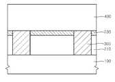
도 1을 참조하면, 반도체 기판(100) 상에 제1절연층(210)을 형성한다. 제1절연층(210)은 실리콘 산화물(SiO2)층이나 실리콘 질화물(Si3N4), 또는 실리콘 탄화물(SiC)와 같은 절연 물질을 포함하는 층간 절연층으로 형성될 수 있다. 제1절연층(210) 상에 후속 식각 과정 등에서 제1절연층(210)을 원하지 않는 침식으로부터 보호하는 식각 정지층(etch stopper: 230)을 더 형성할 수 있다. 식각 정지층(230)은 제1절연층(210)이 실리콘 산화물층을 포함하여 형성될 때, 실리콘 산화물층과 식각 선택비를 가질 수 있는 실리콘 질화물층을 포함하여 형성될 수 있다. 제1절연층(210)이 실리콘 질화물층을 포함하여 형성되는 경우와 같이 식각 정지층(230)은 경우에 따라 생략될 수도 있다.Referring to FIG. 1, a first
반도체 기판(100)에는 디램(DRAM) 소자 또는 낸드 플래시(NAND FLASH) 소자의 메모리 셀(memory cell)을 이루는 셀 트랜지스터(cell transistor: 도시되지 않음)가 구비될 수 있다. 디램 소자의 경우 셀 트랜지스터는 반도체 기판(100) 내에 매몰된 매몰 게이트(buried gate)를 구비한 매몰 게이트를 포함하는 트랜지스터로 구비되어 디램 반도체 소자의 크기 축소에 기여할 수 있다. 셀 트랜지스터가 구비된 반도체 기판(100) 상에 형성되는 제1절연층(210)은 비트 라인(bit line)과 같은 배선과 셀 트랜지스터들을 절연시키는 층간 절연층으로 형성될 수 있다.The
제1절연층(210) 및 식각 정지층(230)을 관통하는 연결 콘택(interconnection contact: 300) 또는 연결 플러그(plug)는 배선과 반도체 기판(100) 연결하여, 셀 트랜지스터의 드레인 영역(drain region)에 배선인 비트 라인을 접속시키도록 형성될 수 있다. 연결 콘택(300)은 도전성 폴리 실리콘(poly silicon)층과 같은 도전층을 포함하여 형성될 수 있으나, 소자의 동작 속도 개선 및 비트 라인 배선의 접속 저항 감소를 위해 텅스텐(W)층과 같은 보다 낮은 저항의 금속층을 포함하여 형성될 수 있다. 제1절연층(210)을 관통하는 관통 콘택홀을 형성한 후, 관통 콘택홀을 채우는 텅스텐층을 증착하고, 텅스텐층을 화학기계적연마(CMP: Chemical Mechanical Polishing) 등으로 평탄화하여 노드(node) 분리함으로써 연결 콘택(300)을 형성할 수 있다. 이때, 평탄화 CMP는 식각 정지층(230) 상에서 연마 정지되도록 수행될 수 있으며, 식각 정지층(230)에 의해서 제1절연층(210)을 이루는 실리콘 산화물층이 CMP 과정 중에 원하지 않은 침식으로부터 보호될 수 있다.A
제1절연층(210) 및 연결 콘택(300)들을 형성한 후, 이들을 덮는 배선 몰드층(400)을 형성한다. 배선 몰드층(400)을 비트 라인과 같은 배선에 패턴 형상을 부여하는 몰드(mold)를 제공하는 층으로 형성될 수 있으며, 후속 과정에서 선택적으로 제거될 희생층으로 형성될 수 있다. 배선 몰드층(400)은 폴리 실리콘층과 같은 실리콘층으로 형성될 수 있다.After forming the first insulating
도 2를 참조하면, 실리콘층을 포함하는 배선 몰드층(400)에 리소그래피(lithography) 및 식각(etch) 과정을 수행하여, 배선 몰드층(400)에 비트 라인과 같은 금속 배선을 위한 트렌치(trench: 411)를 형성한다. 배선 몰드층(400)을 선택적으로 식각함으로써, 배선 몰드층(400)을 길게 라인(line) 형상으로 관통하는 트렌치(411)들을 형성할 수 있다. 이때, 트렌치(411)는 수직한 측벽 프로파일(profile)을 가지게 형성될 수 있으나, 트렌치(411) 바닥의 폭 보다 상측 입구 폭이 상대적으로 넓게 경사진 측벽을 가지게 형성될 수도 있다. 또는 반대로 트렌치(411) 바닥의 폭 보다 상측 입구 폭이 상대적으로 좁게도 형성될 수 있으나, 트렌치(411)를 도전층을 채울 때 채움 특성 개선을 위해서는 수직하거나 또는 입구 폭이 넓게 경사진 측벽 프로파일을 가지는 것이 상대적으로 유효하다. 트렌치(411)를 식각하는 식각 과정은 하부의 식각 정지층(230)이 노출될 때까지 수행되며, 식각 정지층(230)에서 식각이 종료되어 하부의 제1절연층(210)에의 원하지 않는 침식을 억제할 수 있다.Referring to FIG. 2, a lithography and etching process is performed on a
도 3을 참조하면, 트렌치(411)들의 측벽을 덮도록 제1금속층(510)을 형성한다. 제1금속층(510)은 트렌치(411)를 채우는 금속 배선을 이루는 제2금속층과는 다른 금속 원소, 예컨대, 코발트(Co)를 포함하는 층으로 형성될 수 있다. 코발트(Co)를 포함하는 층은 코발트층이나 코발트가 함유된 코발트 합금층으로 형성될 수 있으나, 제2금속층이 구리(Cu)층 또는 구리를 함유하는 층으로 형성될 때, 구리 원자의 이동 또는 확산을 억제하는 데 유효한 코발트층으로 형성될 수 있다. 코발트층은 이동 또는 확산되는 구리 원자를 포획하여 구리 원자와 코발트 원자가 강한 결합을 이루어, 구리 원자의 이동을 억제할 수 있다. 제1금속층(510)은 구리 원자의 이동을 억제하는 관점에서 탄탈륨(Ta)층을 포함하여 형성될 수도 있으나, 구리 원자의 이동을 억제하는 작용과 함께 후속 도입되는 실리사이드화 과정(silicidation) 및 배선 몰드층(400)을 선택적으로 제거하는 과정에서의 내식성을 고려할 때, 코발트층으로 제1금속층(510)을 형성하는 것이 보다 유효하다.Referring to FIG. 3, the
제1금속층(510)은 코발트를 화학기상증착(CVD)함으로써 형성될 수 있으며, 트렌치(411)의 측벽 뿐만 아니라 트렌치(411)의 바닥과 트렌치(411) 바닥에 노출되는 연결 콘택(300)의 상측 표면을 덮게 형성될 수 있다. 연결 콘택(300)이 유효하게 텅스텐층을 포함하여 형성되고, 금속 배선이 구리층을 포함하여 형성되는 점을 고려할 때, 코발트는 텅스텐과 코발트텅스텐(CoW) 합금층을 이루어 연결 콘택(300)으로 구리 이동을 억제할 수 있어, 제1금속층(510)으로 코발트층을 도입하는 것이 보다 유효하다.The
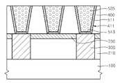
도 4를 참조하면, 제1금속층(510)과 배선 몰드층(400)의 폴리 실리콘층을 실리사이드 반응(silicidation)시켜 제1금속 실리사이드층, 예컨대, 코발트 실리사이드(cobalt silicide, CoSix)층을 포함하는 측벽 보호층(511)을 형성한다. 실리사이드 반응을 위해서 제1금속층(510)에 대해 450℃ 내지 800℃ 온도에서 급속열처리(Rapid Thermal Annealing)와 같은 열처리 과정을 수행하여, 트렌치(411)의 측벽을 덮는 부분에서 폴리 실리콘층과 제1금속층인 코발트층과의 실리사이드 반응을 유도하여 코발트 실리사이드(CoSix)를 포함하는 층을 유도하여 측벽 보호층(511)을 형성한다.Referring to FIG. 4, the polysilicon layer of the
제1금속층(510)이 실리콘층과 접촉하지 않는 부분, 예컨대, 트렌치(411) 바닥에 연장된 제1금속층(510) 부분(513)은 실리사이드화 반응이 이루어지지 않아 코발트를 포함하는 층으로 유지되며, 이러한 부분은 바닥 장벽층(bottom barrier layer: 513)으로 유지된다. 바닥 장벽층(513)은 트렌치(411)를 채울 구리 배선의 구리 원자가 이동 또는 확산되는 것을 억제하는 작용을 하게 된다. 제1금속층(510)이 코발트층 이외의 다른 탄탈륨층을 포함하여 형성될 경우에도, 실리사이드화 반응에 의해 탄탈륨 실리사이드(TaSix)층이 유도되어 측벽 보호층(511)이 형성될 수 있다. 이때, 측벽 보호층(511)을 이루는 제1금속 실리사이드층은 배선 몰드층(400)의 상측 표면 상을 덮게 형성될 수 있다.The portion of the
배선 몰드층(400)을 폴리 실리콘층과 같이 실리콘(Si)을 포함하는 층으로 도입함으로써, 구리 배선에 형상을 제공하는 몰드를 구현하면서 또한 제1금속 실리사이드층이 트렌치(411) 측벽에 자기 정렬되게 형성되도록 유도할 수 있어, 제1금속 실리사이드를 포함하는 측벽 보호층(511)이 구리 배선의 측벽을 자연스럽게 덮어 보호하도록 유도할 수 있다.By introducing the
도 5를 참조하면, 트렌치(411)를 채우는 제2금속층(530)을 형성한다. 제2금속층(530)은 비트 라인과 같은 배선이 낮은 저항을 가지도록 구리(Cu) 또는 구리(Cu)를 포함하는 합금층을 포함하게 형성될 수 있다. 예컨대, 구리 시드(seed)층(531)을 스퍼터링(sputtering) 증착 등으로 형성하고, 구리 시드층(531) 상에 전기 도금(electro-plating)과 같은 전기 화학적 증착(electro chemical deposition)을 수행하여 구리 도금층(533)을 형성하여 제2금속층(530)을 형성할 수 있다. 구리 도금층(533)은 무전해 도금으로 형성될 수 있지만, 화학기상증착으로 구리층을 증착하는 과정을 도입할 수도 있다.Referring to FIG. 5, a second metal layer 530 filling the
도 6을 참조하면, 제2금속층(530)을 CMP 평탄화 과정으로 평탄화하여 개별 제2금속 배선(535)들로 노드 분리(node separation)한다. 이때, CMP 평탄화는 배선 몰드층(400)의 상측 표면이 노출되도록 수행되어 노드 분리가 이루어지게 한다. 이에 따라, 측벽 보호층(511)은 제2금속 배선(535)인 구리 배선의 측벽을 덮어 보호하게 된다. 측벽 보호층(511)을 이루는 코발트 실리사이드층은 구리 원자의 이동을 억제할 수 있어, 제2금속 배선(535)의 구리 원자가 이웃하는 다른 제2금속 배선(535)들 사이로 이동하여 연결되는 브리지(bridge) 현상이 유발되는 것을 유효하게 억제할 수 있다. 코발트 실리사이드층 이외에 탄탈륨 실리사이드층 또한 이러한 구리 원자의 이동을 억제하는 효과를 유도할 수 있다.Referring to FIG. 6, the second metal layer 530 is planarized by a CMP planarization process to node separation into individual
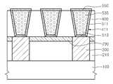
도 7을 참조하면, 제2금속 배선(535)의 노출된 상측 표면에 상측 보호층(550)을 형성한다. 제2금속 배선(535)의 구리층의 표면 상에 코발트(Co)층 또는 코발트를 포함하는 합금층, 예컨대, 코발트텅스텐인 합금(CoWP)층, 코발트텅스텐 합금(CoW)층, 코발트텅스텐보론 합금(CoWB)층 또는 코발트텅스텐인보론 합금(CoWPB)층을 증착하여 상측 보호층(550)을 형성한다. 상측 보호층(550)은 구리 원자의 이동을 억제하고, 또한, 구리 배선의 산화를 방지하는 장벽층으로 형성되며, 구리 원자의 이동을 억제하는 효과 및 구리 배선의 오염 방지를 고려할 때, 코발트텅스텐인(CoWP) 합금층을 포함하게 상측 보호층(550)을 형성하는 것이 보다 유효하다. 상측 보호층(550)은 제2금속 배선(535)이 구리 배선에 선택적으로 증착이 이루어질 수 있는 코발트를 화학기상증착(CVD)하거나 또는 CoWP를 CVD 증착하여, 부가적인 노드 분리를 생략하며 제2금속 배선(535)을 덮게 형성될 수 있다.Referring to FIG. 7, an upper
도 8을 참조하면, 상측 보호층(550)에 노출된 배선 몰드층(400)을 선택적으로 제거하여 제2금속 배선(535)들 사이의 갭(gap: 403) 공간을 노출시킨다. 배선 몰드층(400)을 이루는 폴리 실리콘층을 딥 아웃(dip out)시킴으로써, 제2금속 배선(535)의 측벽 보호층(511)의 외측 표면이 노출되도록 한다.Referring to FIG. 8, the
바닥 장벽층(513)을 유효하게 이루는 코발트(Co)를 포함하는 층, 예컨대, 코발트층에 식각 선택비를 가지고, 또한, 측벽 보호층(511)을 유효하게 이루는 코발트 실리사이드(CoSix)를 포함하는 층에 대해 식각 선택비를 가지며, 폴리 실리콘층의 배선 몰드층(400)을 선택적으로 제거하여, 식각 과정에서 제2금속 배선(535)을 이루는 구리층이 원하지 않게 침식되는 것을 억제하고, 또한, 식각 과정에서 측벽 보호층(511) 또는 바닥 장벽층(513)이 손실되지 않도록 한다. 또한, 상측 보호층(550)을 이루는 코발트층이나 CoWP층이 식각 과정에 손상되지 않도록 식각 과정을 수행한다.A layer including cobalt (Co) that effectively forms the
폴리 실리콘층이 선택적으로 제거되도록, 질산(HNO3) 및 불산(HF), 탈이온수(DI water)를 포함하거나 또는 수산화암모늄(NH4OH)을 포함하는 식각액을 사용하는 습식 식각을 수행하여, 배선 몰드층(400)을 선택적으로 제거한다. 코발트 실리사이드층은 산화에 대한 저항성이 크고 내식성이 우수한 것으로 평가되므로, 배선 몰드층(400)을 제거하는 과정에서 측벽 보호층(511)이 손상되는 것을 유효하게 억제할 수 있다. 이러한 습식 식각 이외에 식각 선택비를 구현하는 다른 선택적 식각 과정도 배선 몰드층(400)을 제거하는 과정에 도입될 수 있으나, 측벽 보호층(511) 및 상측 보호층(550)의 손상을 유효하게 억제하는 습식 식각이 배선 몰드층(400)을 이루는 폴리 실리콘층을 선택적으로 제거하는 데 보다 유효하게 평가되고 있다.Wet etching using an etchant containing nitric acid (HNO3 ), hydrofluoric acid (HF), DI water, or ammonium hydroxide (NH4 OH), to selectively remove the polysilicon layer, The
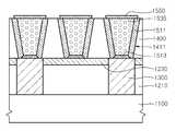
도 9를 참조하면, 제2금속 배선(535)들 사이를 절연시키기 위해서, 제2금속 배선(535)들을 덮는 제2절연층(450)을 형성한다. 제2절연층(450)은 제2금속 배선(535)의 상측 보호층(550)을 덮고, 또한, 측벽 보호층(511)을 덮게 연장될 수 있다. 이때, 제2금속 배선(535)들 사이의 갭(403)을 제2절연층(450)이 완전히 채우지 않고, 갭(403) 내측에 공극(void)과 같은 빈 공간, 예컨대, 에어 갭(air gap: 405)을 유발하도록, 제2절연층(450)을 증착한다. 반도체 소자의 회로 패턴 피치(pitch)가 축소되고, 패턴들 간의 간격, 즉, 제2금속 배선(535)들 간의 간격이 급격히 감소되고 있어, 단차 도포성(step coverage)이 취약한 증착 과정을 도입하여 제2절연층(450)을 증착할 경우, 내부에 공극과 같은 빈 공간이 에어 갭(405)으로 자연히 유발될 수 있다.Referring to FIG. 9, in order to insulate the
제2절연층(450)은 단차 도포성이 취약한 것으로 일반적으로 평가되는 플라즈마 개선 화학기상증착(Plasma Enhanced CVD)로 실리콘 산화물층 또는 실리콘 질화물층을 증착하여 형성될 수 있다. 제2절연층(450)의 내부에 에어 갭(405)이 공극 등으로 유발되는 현상은, 단차 도포성이 취약한 증착 과정에서 제2금속 배선(535)의 상측 모서리 부분, 즉, 상측 보호층(550)의 가장자리 부분에서 오버 행(over hang)이 우선적으로 유발되고, 이에 따라 갭(403) 내측으로 절연 물질의 증착이 오버 행 부분에 의해 방해되는 작용에 의해 설명될 수 있다. 따라서, 에어 갭(405)의 크기 및 부피를 의도적으로 확대시키기 위해서, 오버행을 의도적으로 유도하기 위해, 제2금속 배선(535)의 상측 단부의 폭이 하측 단부의 폭보다 넓어 경사진 측벽을 가지는 형상을 가지도록 제2금속 배선(535)의 형상을 변경할 수 있다. 이를 위해서, 제2금속 배선(535)에 형상을 제공하는 트렌치(411)를 바닥 폭 보다 상측 입구 폭이 넓어 경사진 측벽을 가지게 형성할 수 있다.The second
제2절연층(450)의 내측에 유발된 에어 갭(405)은 빈 공간으로서, 제2금속 배선(535)들을 절연시키는 제2절연층(450)을 이루는 실리콘 산화물층이나 실리콘 질화물층에 비해 낮은 유전율을 제공하게 된다. 이에 따라, 제2금속 배선(535)들 사이를 절연하는 제2절연층(450) 및 에어 갭(405)을 포함하는 절연체 구조는, 제2절연층(450)만으로 이루어지는 절연체 구조에 비해 낮은 유절율을 나타내게 되므로, 유전율 감소에 의해 기생 커패시턴스의 감소를 유도할 수 있어 RC 지연을 억제하여 소자의 동작 속도를 개선할 수 있다.The
반도체 기판(100) 상의 제1절연층(210) 상에 형성된 제2금속의 배선(535)들, 측벽 보호층(511), 상측 보호층(550), 및 에어 갭(405)을 가지는 제2절연층(450)을 포함하는 반도체 소자의 배선 구조체는, 측벽 보호층(511)을 제1금속 실리사이드층을 포함하여 형성하는 과정을 다양하게 변형시켜 구현할 수 있다.A
도 10 내지 도 13은 본 출원의 일 실시예에 따른 반도체 소자의 배선 구조체 및 제조 방법의 변형예를 보여주는 도면들이다.10 to 13 are views illustrating a modified example of a wiring structure and a manufacturing method of a semiconductor device according to an embodiment of the present application.
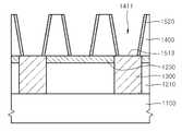
도 10을 참조하면, 도 1 내지 도 2를 참조하여 설명한 바와 마찬가지로, 반도체 기판(1100) 상에 제1절연층(1210) 및 연결 콘택(1300), 식각 정지층(1230), 배선 몰드층(1400), 트렌치(1411)을 형성한다. 이때, 배선 몰드층(1400)은 폴리 실리콘층과 같은 실리콘층을 포함하게 형성되지 않고, 다른 절연층, 예컨대, 실리콘 산화물층이나 실리콘 질화물층, 실리콘 탄화물층 등을 희생층으로 형성할 수 있다. 트렌치(1411) 측벽에 제1금속 실리사이드층을 위한 실리사이드화 반응에 참여할 실리콘층을 포함하는 측벽 스페이서(1520)을 별도로 형성한다. 측벽 스페이서(1520)는 폴리 실리콘층을 증착한 후 스페이서 식각(spacer etch) 또는 이방성 식각을 수행하여 형성될 수 있다. 측벽 스페이서(1520)는 스페이서 식각 과정을 생략하여 트렌치(1411)의 바닥을 덮게 연장되는 형상을 가질 수도 있으나, 연결 콘택(1230)과의 접촉 저항 개선을 위해서 연결 콘택(1230)의 상측 표면을 노출하도록 형성되는 것이 보다 유효하다.Referring to FIG. 10, as described with reference to FIGS. 1 and 2, the first insulating
도 11을 참조하면, 도 3을 참조하여 설명한 바와 마찬가지로, 트렌치(1411) 측벽 및 바닥을 덮어, 측벽 스페이서(1520)과 접촉하여 덮도록 제1금속층(1510)을 형성한다. 도 3의 경우 제1금속층(도 3의 510)이 폴리 실리콘층의 몰드 배선층(도 3의 400)의 측벽에 직접적으로 접촉하게 형성되지만, 도 11의 제1금속층(1510)은 측벽 스페이서(1520)를 이루는 폴리 실리콘층과 접촉하도록 형성될 수 있다.Referring to FIG. 11, as described with reference to FIG. 3, the
도 12를 참조하면, 도 4를 참조하여 설명한 바와 마찬가지로, 실리사이드화 반응을 유도하는 열처리를 수행하여, 측벽 스페이서(1520)와 접촉하는 제1금속층(1510) 부분이 측벽 스페이서(1520)의 실리콘과 반응하여 제1금속 실리사이드, 예컨대, 코발트 실리사이드층으로 전환되도록 하여 측벽 보호층(1511)을 형성한다. 이때, 제1금속층(1510)의 트렌치(1411) 바닫을 덮는 부분은 마찬가지로 바닥 장벽층(1513)으로 유지된다.Referring to FIG. 12, as described with reference to FIG. 4, the
도 13을 참조하면, 도 5 내지 도 7을 참조하여 설명한 바와 마찬가지로, 구리층을 포함하는 제2금속 배선(1535)들을 형성하고, 제2금속 배선(1535)의 상측 표면을 덮어 보호하는 상측 보호층(1550)을 형성한다. 연후에, 도 8을 참조하여 설명한 바와 마찬가지로, 배선 몰드층(1400)을 선택적으로 제거한다. 이때, 배선 몰드층(1400)이 실리콘층이 아닌 실리콘 산화물층이나 실리콘 질화물층을 포함하여 형성되고 있으므로, 실리콘 산화물층이나 실리콘 질화물층을 선택적으로 제거할 수 있는 식각 과정을 도입하여 선택적으로 제거한다. 이후에, 도 9를 참조하여 설명한 바와 같이 제2절연층(도 9의 450)을 제2금속 배선(1535)들을 절연하게 에어 갭(405)를 포함하도록 형성할 수 있다.Referring to FIG. 13, as described with reference to FIGS. 5 to 7, upper protection for forming
상술한 바와 같이 본 출원의 실시 형태들을 도면들을 예시하며 설명하지만, 이는 본 출원에서 제시하고자 하는 바를 설명하기 위한 것이며, 세밀하게 제시된 형상으로 본 출원에서 제시하고자 하는 바를 한정하고자 한 것은 아니다. 본 출원에서 제시한 기술적 사상이 반영되는 한 다양한 다른 변형예들이 가능할 것이다.Although the embodiments of the present application as described above illustrate and describe the drawings, it is intended to illustrate what is being suggested in the present application and is not intended to limit what is presented in the present application in a detailed form. Various other modifications will be possible as long as the technical ideas presented in this application are reflected.
100: 반도체 기판, 210: 제1절연층,
300: 연결 콘택, 400: 배선 몰드층,
405 : 에어 갭(air gap),450 : 제2절연층,
511 : 측벽 보호층, 535 : 금속 배선
550 : 상측 보호층.100: semiconductor substrate, 210: first insulating layer,
300: connection contact, 400: wiring mold layer,
405: air gap, 450: second insulating layer,
511: side wall protective layer, 535: metal wiring
550: upper protective layer.
Claims (38)
Translated fromKorean상기 제1절연층 상에 배선을 위한 트렌치(trench)들을 제공하는 배선 몰드(mold)층을 형성하는 단계;
상기 트렌치들의 측벽에 제1금속의 실리사이드(silicide)층을 포함하는 측벽 보호층을 형성하는 단계;
상기 트렌치들을 채우는 제2금속 배선들을 형성하는 단계;
상기 제2금속 배선들의 상측 표면을 보호하는 상측 보호층을 형성하는 단계;
상기 상측 및 측벽 보호층들로 상기 제2금속 배선들을 보호하며 상기 배선 몰드층을 선택적으로 제거하는 단계; 및
상기 제2금속 배선들 사이에 에어 갭(air gap)을 가지는 제2절연층을 형성하는 단계를 포함하는 반도체 소자의 배선 구조체 제조 방법.
Forming a first insulating layer on the semiconductor substrate;
Forming a wiring mold layer on the first insulating layer to provide trenches for wiring;
Forming a sidewall protection layer comprising a silicide layer of a first metal on the sidewalls of the trenches;
Forming second metal wires filling the trenches;
Forming an upper protective layer protecting upper surfaces of the second metal wires;
Protecting the second metal interconnections with the upper and sidewall protection layers and selectively removing the interconnect mold layer; And
Forming a second insulating layer having an air gap between the second metal wires.
상기 제2금속 배선들을 형성하는 단계는
상기 트렌치를 채우는 구리(Cu)층을 형성하는 단계를 포함하는 반도체 소자의 배선 구조체 제조 방법.
The method of claim 1,
Forming the second metal wires
And forming a copper (Cu) layer filling the trench.
상기 제1금속 실리사이드층은
상기 구리(Cu)층의 구리 원자의 이동을 억제하는 코발트 실리사이드(CoSix)층을 포함하여 형성되는 반도체 소자의 배선 구조체 제조 방법.
The method of claim 2,
The first metal silicide layer is
A method of manufacturing a wiring structure for a semiconductor device, comprising a cobalt silicide (CoSix ) layer that suppresses movement of copper atoms in the copper (Cu) layer.
상기 제1금속 실리사이드층은
상기 구리(Cu)층의 구리 원자의 이동을 억제하는 탄탈륨 실리사이드(TaSix)을 포함하여 형성되는 반도체 소자의 배선 구조체 제조 방법.
The method of claim 2,
The first metal silicide layer is
A tantalum silicide (TaSix ) that suppresses the movement of copper atoms in the copper (Cu) layer is formed.
상기 상측 보호층은
코발트층 또는 코발트를 포함하는 합금층을 포함하여 형성되는 반도체 소자의 배선 구조체 제조 방법.
The method of claim 1,
The upper protective layer
A method of manufacturing a wiring structure for a semiconductor device, comprising a cobalt layer or an alloy layer containing cobalt.
상기 코발트를 포함하는 합금층은
코발트텅스텐인 합금(CoWP)층, 코발트텅스텐 합금(CoW)층, 코발트텅스텐보론 합금(CoWB)층 및 코발트텅스텐인보론 합금(CoWPB)층을 포함하여 이루어지는 일군에서 선택된 어느 하나의 합금층을 포함하여 형성되는 반도체 소자의 배선 구조체 제조 방법.
The method of claim 5,
The alloy layer containing the cobalt
Including a cobalt tungsten alloy (CoWP) layer, a cobalt tungsten alloy (CoW) layer, a cobalt tungsten boron alloy (CoWB) layer and a cobalt tungsten in boron alloy (CoWPB) layer comprising any one alloy layer selected from the group consisting of The manufacturing method of the wiring structure of the semiconductor element formed.
상기 제2절연층을 형성하는 단계는
상기 제2금속 배선들 상에 절연 물질을 증착하되,
상기 제2금속 배선들의 상측 모서리 부분에 오버행(over hang)이 유도되어 상기 제2금속 배선들 사이 갭(gap)들의 내측에 공극(void)이 유발되어 상기 에어 갭(air gap)으로 형성되도록 하는 단계를 포함하는 반도체 소자의 배선 구조체 제조 방법.
The method of claim 1,
Forming the second insulating layer
Deposit an insulating material on the second metal wires;
An overhang is induced in an upper edge portion of the second metal wires to cause voids inside the gaps between the second metal wires so as to form the air gap. Method of manufacturing a wiring structure of a semiconductor device comprising the step.
상기 제2절연층을 형성하는 단계는
상기 제2금속 배선들 사이에 상기 에어 갭이 공극으로 유발되게 실리콘 산화물 또는 실리콘 질화물을 화학기상증착(CVD)하는 단계를 포함하는 반도체 소자의 배선 구조체 제조 방법.
The method of claim 7, wherein
Forming the second insulating layer
Chemical vapor deposition (CVD) of silicon oxide or silicon nitride such that the air gap is caused to form a gap between the second metal wires.
상기 제2금속 배선은
상기 오버행의 유도를 위해 상측 단부의 폭이 하측 단부의 폭보다 넓게 경사진 측벽을 가지게 형성되는 반도체 소자의 배선 구조체 제조 방법.
The method of claim 7, wherein
The second metal wiring
The method of manufacturing a wiring structure of a semiconductor device is formed so that the width of the upper end is inclined wider than the width of the lower end to induce the overhang.
상기 트렌치는
상기 제2금속 배선이 상기 경사진 측벽을 가지도록
바닥 폭 보다 상측 입구 폭이 넓게 경사진 측벽을 가지게 형성되는 반도체 소자의 배선 구조체 제조 방법.
10. The method of claim 9,
The trench
So that the second metal wire has the inclined sidewall
A method for manufacturing a wiring structure of a semiconductor device, which is formed to have a sidewall inclined to have a wider inlet width than a bottom width.
상기 제1절연층 상에 배선을 위한 트렌치(trench)들을 제공하는 배선 몰드(mold)층을 실리콘(Si)층을 포함하여 형성하는 단계;
상기 트렌치들의 측벽을 덮는 제1금속층을 형성하는 단계;
상기 제1금속층과 상기 실리콘층을 실리사이드 반응(silicidation)시켜 제1금속 실리사이드층을 포함하는 측벽 보호층을 형성하는 단계;
상기 트렌치들을 채우는 제2금속 배선들을 형성하는 단계;
상기 제2금속 배선들의 상측 표면을 보호하는 상측 보호층을 형성하는 단계;
상기 측벽 및 상측 보호층들에 의해 상기 제2금속 배선들을 보호하며 상기 배선 몰드층을 선택적으로 제거하는 단계; 및
상기 제2금속 배선들 사이에 에어 갭(air gap)을 가지는 제2절연층을 형성하는 단계를 포함하는 반도체 소자의 배선 구조체 제조 방법.
Forming a first insulating layer on the semiconductor substrate;
Forming a wiring mold layer including a silicon (Si) layer on the first insulating layer to provide trenches for wiring;
Forming a first metal layer covering sidewalls of the trenches;
Silicidating the first metal layer and the silicon layer to form a sidewall protective layer including a first metal silicide layer;
Forming second metal wires filling the trenches;
Forming an upper protective layer protecting upper surfaces of the second metal wires;
Selectively protecting the second metal interconnections by the sidewalls and the upper passivation layers and removing the interconnection mold layer; And
Forming a second insulating layer having an air gap between the second metal wires.
상기 배선 몰드층을 형성하는 단계 이전에
상기 제1절연층을 관통하여 상기 반도체 기판 및 상기 제2금속 배선을 연결하는 연결 콘택(contact)을 형성하는 단계를 더 포함하는 반도체 소자의 배선 구조체 제조 방법.
12. The method of claim 11,
Before forming the wiring mold layer
And forming a connection contact between the semiconductor substrate and the second metal wire through the first insulating layer.
상기 배선 몰드(mold)층을 형성하는 단계는
상기 제1절연층 상에 상기 실리콘층을 증착하는 단계; 및
상기 실리콘층을 선택적으로 식각하여 관통하는 상기 트렌치(trench)들을 형성하여 상기 제1금속층에 접촉할 상기 트렌치의 측벽들을 상기 실리콘층 부분으로 제공하는 단계를 포함하는 반도체 소자의 배선 구조체 제조 방법.
12. The method of claim 11,
Forming the wiring mold layer
Depositing the silicon layer on the first insulating layer; And
Selectively etching the silicon layer to form the trenches to provide sidewalls of the trench to be in contact with the first metal layer as the silicon layer portion.
상기 제1금속층을 형성하는 단계는
상기 트렌치의 측벽을 제공하는 상기 실리콘층 부분에 접촉되게 코발트(Co)를 포함하는 층을 형성하는 단계를 포함하는 반도체 소자의 배선 구조체 제조 방법.
The method of claim 13,
Forming the first metal layer is
Forming a layer comprising cobalt (Co) in contact with the portion of the silicon layer providing the sidewalls of the trench.
상기 코발트(Co)를 포함하는 층은
코발트(Co)층을 증착하여 형성되는 반도체 소자의 배선 구조체 제조 방법.
15. The method of claim 14,
The layer containing cobalt (Co)
A method for manufacturing a wiring structure of a semiconductor device formed by depositing a cobalt (Co) layer.
상기 코발트(Co)를 포함하는 층은 상기 트렌치의 바닥을 덮도록 연장되게 형성되는 반도체 소자의 배선 구조체 제조 방법.
16. The method of claim 15,
The layer including the cobalt (Co) is formed to extend so as to cover the bottom of the trench.
상기 측벽 보호층을 형성하는 단계는
상기 코발트(Co)를 포함하는 층에 대해 열처리를 수행하여 상기 트렌치의 측벽을 덮는 부분에 상기 실리사이드 반응을 유도하여 상기 제1금속 실리사이드층을 코발트 실리사이드(CoSix)를 포함하는 층으로 유도하고,
상기 트렌치 바닥에 연장된 부분은 상기 코발트를 포함하는 층으로 유지되게 하여 바닥 장벽층(bottom barrier layer)으로 사용하는 단계를 포함하는 반도체 소자의 배선 구조체 제조 방법.
17. The method of claim 16,
Forming the sidewall protective layer
Heat-treating the layer containing the cobalt (Co) to induce the silicide reaction in a portion covering the sidewall of the trench to induce the first metal silicide layer to a layer containing cobalt silicide (CoSix ),
And a portion extending to the bottom of the trench is maintained as a layer including the cobalt and used as a bottom barrier layer.
상기 열처리는
450℃ 내지 800℃ 온도에서 급속열처리(Rapid Thermal Annealing)으로 수행되는 반도체 소자의 배선 구조체 제조 방법.
18. The method of claim 17,
The heat treatment
Method of manufacturing a wiring structure of a semiconductor device which is carried out by rapid thermal annealing at 450 ℃ to 800 ℃ temperature.
상기 배선 몰드층을 선택적으로 제거하는 단계는
상기 코발트(Co)를 포함하는 층 및 상기 코발트 실리사이드(CoSix)를 포함하는 층에 대해 식각 선택비를 가지며 상기 실리콘층을 선택적으로 제거하도록 질산(HNO3) 및 불산(HF), 탈이온수(DI water)를 포함하거나 또는 수산화암모늄(NH4OH)을 포함하는 식각액을 사용하는 습식 식각으로 수행되는 반도체 소자의 배선 구조체 제조 방법.
18. The method of claim 17,
Selectively removing the wiring mold layer
Nitric acid (HNO3 ), hydrofluoric acid (HF), and deionized water (HNO3 ) to have an etch selectivity with respect to the layer containing cobalt (Co) and the layer containing cobalt silicide (CoSix ) and to selectively remove the silicon layer. DI water) or a method for manufacturing a wiring structure of a semiconductor device performed by wet etching using an etchant containing ammonium hydroxide (NH4 OH).
상기 제2금속의 배선들을 형성하는 단계는
상기 트렌치를 채우는 구리(Cu)층을 형성하는 단계를 포함하는 반도체 소자의 배선 구조체 제조 방법.
12. The method of claim 11,
Forming the wires of the second metal
And forming a copper (Cu) layer filling the trench.
상기 상측 보호층을 형성하는 단계는
상기 구리층의 표면 상에 코발트(Co)층 또는 코발트텅스텐인(CoWP) 합금층을 화학기상증착(CVD)으로 선택적 증착하는 단계를 포함하는 반도체 소자의 배선 구조체 제조 방법.
21. The method of claim 20,
Forming the upper protective layer is
And selectively depositing a cobalt (Co) layer or a cobalt tungsten (CoWP) alloy layer on the surface of the copper layer by chemical vapor deposition (CVD).
상기 제1절연층 상에 배선을 위한 트렌치(trench)들을 제공하는 배선 몰드(mold)층을 형성하는 단계;
상기 트렌치의 측벽에 실리콘(Si)층을 포함하는 측벽 스페이서(spacer)를 형성하는 단계;
상기 측벽 스페이서를 덮는 제1금속층을 형성하는 단계;
상기 제1금속층과 상기 실리콘층을 실리사이드 반응(silicidation)시켜 제1금속 실리사이드층을 포함하는 측벽 보호층을 형성하는 단계;
상기 트렌치들을 채우는 제2금속 배선들을 형성하는 단계;
상기 제2금속 배선들의 상측 표면을 보호하는 상측 보호층을 형성하는 단계;
상기 측벽 및 상측 보호층들에 의해 상기 제2금속 배선들을 보호하며 상기 배선 몰드층을 선택적으로 제거하는 단계; 및
상기 제2금속 배선들 사이에 에어 갭(air gap)을 가지는 제2절연층을 형성하는 단계를 포함하는 반도체 소자의 배선 구조체 제조 방법.
Forming a first insulating layer on the semiconductor substrate;
Forming a wiring mold layer on the first insulating layer to provide trenches for wiring;
Forming a sidewall spacer comprising a silicon (Si) layer on the sidewalls of the trench;
Forming a first metal layer covering the sidewall spacers;
Silicidating the first metal layer and the silicon layer to form a sidewall protective layer including a first metal silicide layer;
Forming second metal wires filling the trenches;
Forming an upper protective layer protecting upper surfaces of the second metal wires;
Selectively protecting the second metal interconnections by the sidewalls and the upper passivation layers and removing the interconnection mold layer; And
Forming a second insulating layer having an air gap between the second metal wires.
상기 제1금속층을 형성하는 단계는
상기 측벽 스페이서에 접촉하는 코발트(Co)를 포함하는 층을 형성하는 단계를 포함하는 반도체 소자의 배선 구조체 제조 방법.
The method of claim 22,
Forming the first metal layer is
Forming a layer comprising cobalt (Co) in contact with the sidewall spacers.
상기 코발트(Co)를 포함하는 층은 상기 측벽 스페이서에 노출되는 상기 트렌치의 바닥을 덮도록 연장되게 형성되는 반도체 소자의 배선 구조체 제조 방법.
24. The method of claim 23,
The layer including the cobalt (Co) is formed to extend to cover the bottom of the trench exposed to the sidewall spacers.
상기 측벽 보호층을 형성하는 단계는
상기 코발트(Co)를 포함하는 층에 대해 열처리를 수행하여 상기 측벽 스페이서와 상기 실리사이드 반응을 유도하여 상기 제1금속 실리사이드층을 코발트 실리사이드(CoSix)를 포함하는 층으로 유도하고,
상기 트렌치 바닥에 연장된 부분은 상기 코발트를 포함하는 층으로 유지되게 하여 바닥 장벽층(bottom barrier layer)으로 사용하는 단계를 포함하는 반도체 소자의 배선 구조체 제조 방법.
24. The method of claim 23,
Forming the sidewall protective layer
Heat-treating the layer containing the cobalt (Co) to induce the silicide reaction with the sidewall spacer to induce the first metal silicide layer to a layer containing cobalt silicide (CoSix ),
And a portion extending to the bottom of the trench is maintained as a layer including the cobalt and used as a bottom barrier layer.
상기 제2금속 배선들 측벽을 덮는 제1금속 실리사이드(silicide)층을 포함하는 측벽 보호층;
상기 제2금속 배선들의 상측 표면을 덮는 상측 보호층; 및
상기 제2금속 배선들 사이에 에어 갭(air gap)을 가지고 상기 상측 보호층을 덮는 제2절연층을 포함하는 반도체 소자의 배선 구조체.
Second metal wires formed on the first insulating layer on the semiconductor substrate;
A sidewall protection layer including a first metal silicide layer covering sidewalls of the second metal wires;
An upper protective layer covering upper surfaces of the second metal wires; And
And a second insulating layer covering the upper protective layer with an air gap between the second metal lines.
상기 제1절연층을 관통하여 상기 반도체 기판 및 상기 제2금속 배선을 연결하는 연결 콘택(contact)을 더 포함하는 반도체 소자의 배선 구조체.
The method of claim 26,
And a connection contact between the semiconductor substrate and the second metal wire through the first insulating layer.
상기 제1절연층과 상기 제2금속 배선의 계면에 코발트(Co)를 포함하는 층으로 도입된 바닥 장벽층(bottom barrier layer)을 더 포함하는 반도체 소자의 배선 구조체.
The method of claim 26,
And a bottom barrier layer introduced as a layer containing cobalt (Co) at an interface between the first insulating layer and the second metal wiring.
상기 코발트(Co)를 포함하는 층은
코발트(Co)층을 포함하는 반도체 소자의 배선 구조체.
29. The method of claim 28,
The layer containing cobalt (Co)
A wiring structure of a semiconductor device comprising a cobalt (Co) layer.
상기 제2금속 배선들은
구리(Cu)층을 포함하는 반도체 소자의 배선 구조체.
The method of claim 26,
The second metal wires
A wiring structure of a semiconductor device comprising a copper (Cu) layer.
상기 제1금속 실리사이드층은
상기 구리(Cu)층의 구리 원자의 이동을 억제하는 코발트 실리사이드(CoSix)층을 포함하는 반도체 소자의 배선 구조체.
The method of claim 26,
The first metal silicide layer is
The wiring structure of the semiconductor element containing the cobalt silicide (CoSix ) layer which suppresses the movement of the copper atom of the said copper (Cu) layer.
상기 제1금속 실리사이드층은
상기 구리(Cu)층의 구리 원자의 이동을 억제하는 탄탈륨 실리사이드(TaSix)을 포함하는 반도체 소자의 배선 구조체.
The method of claim 26,
The first metal silicide layer is
The wiring structure of the semiconductor element containing tantalum silicide (TaSix ) which suppresses movement of the copper atom of the said copper (Cu) layer.
상기 상측 보호층은
코발트층 또는 코발트(Co)를 포함하는 합금층을 포함하는 반도체 소자의 배선 구조체.
The method of claim 26,
The upper protective layer
A wiring structure of a semiconductor device comprising a cobalt layer or an alloy layer containing cobalt (Co).
상기 제2절연층은
상기 제2금속 배선들 사이에 상기 에어 갭이 공극으로 유발하게 화학기상증착(CVD)된 실리콘 산화물층 또는 실리콘 질화물층을 포함하는 반도체 소자의 배선 구조체.
The method of claim 26,
The second insulating layer is
And a silicon oxide layer or a silicon nitride layer chemically vapor deposited (CVD) such that the air gap is caused to form a gap between the second metal lines.
상기 제2금속 배선은
상기 제2절연층에 상기 에어 갭을 유도하기 위해 상측 단부의 폭이 하측 단부의 폭보다 넓게 경사진 측벽을 가지게 형성된 반도체 소자의 배선 구조체.
35. The method of claim 34,
The second metal wiring is
And a sidewall having an inclined sidewall wider than the width of the lower end to induce the air gap in the second insulating layer.
상기 구리 배선들 측벽을 덮는 코발트 실리사이드(cobalt silicide)층을 포함하는 측벽 보호층;
상기 구리 배선들의 상측 표면을 덮는 상측 보호층; 및
상기 구리 배선들 사이에 에어 갭(air gap)을 가지고 상기 상측 보호층을 덮는 제2절연층을 포함하는 반도체 소자의 배선 구조체.
Copper (Cu) wirings formed on the first insulating layer on the semiconductor substrate;
A sidewall protection layer comprising a cobalt silicide layer covering sidewalls of the copper wires;
An upper protective layer covering an upper surface of the copper wires; And
And a second insulating layer covering the upper passivation layer with an air gap between the copper wires.
상기 제1절연층과 상기 구리 배선의 계면에 코발트(Co)층을 포함하여 도입된 바닥 장벽층(bottom barrier layer)을 더 포함하는 반도체 소자의 배선 구조체.
37. The method of claim 36,
And a bottom barrier layer including a cobalt layer at an interface between the first insulating layer and the copper wiring.
상기 구리 배선은
비트 라인(bit line)인 반도체 소자의 배선 구조체.
37. The method of claim 36,
The copper wiring is
A wiring structure of a semiconductor device that is a bit line.
Priority Applications (3)
| Application Number | Priority Date | Filing Date | Title |
|---|---|---|---|
| KR1020120014459AKR20130092884A (en) | 2012-02-13 | 2012-02-13 | Interconnection structure in semiconductor device and manufacturing method for the same |
| US13/586,985US20130207267A1 (en) | 2012-02-13 | 2012-08-16 | Interconnection structures in a semiconductor device and methods of manufacturing the same |
| US14/626,135US9379009B2 (en) | 2012-02-13 | 2015-02-19 | Interconnection structures in a semiconductor device and methods of manufacturing the same |
Applications Claiming Priority (1)
| Application Number | Priority Date | Filing Date | Title |
|---|---|---|---|
| KR1020120014459AKR20130092884A (en) | 2012-02-13 | 2012-02-13 | Interconnection structure in semiconductor device and manufacturing method for the same |
Publications (1)
| Publication Number | Publication Date |
|---|---|
| KR20130092884Atrue KR20130092884A (en) | 2013-08-21 |
Family
ID=48944949
Family Applications (1)
| Application Number | Title | Priority Date | Filing Date |
|---|---|---|---|
| KR1020120014459AWithdrawnKR20130092884A (en) | 2012-02-13 | 2012-02-13 | Interconnection structure in semiconductor device and manufacturing method for the same |
Country Status (2)
| Country | Link |
|---|---|
| US (2) | US20130207267A1 (en) |
| KR (1) | KR20130092884A (en) |
Cited By (4)
| Publication number | Priority date | Publication date | Assignee | Title |
|---|---|---|---|---|
| KR20150073595A (en)* | 2013-12-23 | 2015-07-01 | 삼성전자주식회사 | Wiring structure in a semiconductor device and method for forming the same |
| US9728604B2 (en) | 2015-04-09 | 2017-08-08 | Samsung Electronics Co., Ltd. | Semiconductor devices |
| KR20190096449A (en)* | 2017-01-13 | 2019-08-19 | 어플라이드 머티어리얼스, 인코포레이티드 | Methods and apparatus for low temperature silicon nitride films |
| US10559571B2 (en) | 2017-04-13 | 2020-02-11 | Samsung Electronics Co., Ltd. | Methods of fabricating semiconductor memory devices |
Families Citing this family (30)
| Publication number | Priority date | Publication date | Assignee | Title |
|---|---|---|---|---|
| KR101934864B1 (en)* | 2012-05-30 | 2019-03-18 | 삼성전자주식회사 | Through silicon via structure, methods of forming the same, image sensor including the through silicon via structure and methods of manufacturing the image sensor |
| KR102003881B1 (en)* | 2013-02-13 | 2019-10-17 | 삼성전자주식회사 | Semiconductor deivces and methods of fabricating the same |
| US8889506B1 (en)* | 2013-06-28 | 2014-11-18 | Stmicroelectronics, Inc. | Structure and method for interconnect spatial frequency doubling using selective ridges |
| KR102119829B1 (en)* | 2013-09-27 | 2020-06-05 | 에스케이하이닉스 주식회사 | Semiconductor device and menufacturing method of the same |
| CN103633021B (en)* | 2013-12-02 | 2015-12-30 | 上海华力微电子有限公司 | A kind of method preparing air gap copper interconnection structure |
| US9214429B2 (en)* | 2013-12-05 | 2015-12-15 | Stmicroelectronics, Inc. | Trench interconnect having reduced fringe capacitance |
| US20150162277A1 (en) | 2013-12-05 | 2015-06-11 | International Business Machines Corporation | Advanced interconnect with air gap |
| US9312168B2 (en) | 2013-12-16 | 2016-04-12 | Applied Materials, Inc. | Air gap structure integration using a processing system |
| US9396989B2 (en)* | 2014-01-27 | 2016-07-19 | Applied Materials, Inc. | Air gaps between copper lines |
| KR20150091895A (en)* | 2014-02-04 | 2015-08-12 | 에스케이하이닉스 주식회사 | Semiconductor device and method of operating the same |
| US9583380B2 (en)* | 2014-07-17 | 2017-02-28 | Globalfoundries Inc. | Anisotropic material damage process for etching low-K dielectric materials |
| US9401305B2 (en)* | 2014-11-05 | 2016-07-26 | Sandisk Technologies Llc | Air gaps structures for damascene metal patterning |
| US9847249B2 (en)* | 2014-11-05 | 2017-12-19 | Sandisk Technologies Llc | Buried etch stop layer for damascene bit line formation |
| US20160225652A1 (en) | 2015-02-03 | 2016-08-04 | Applied Materials, Inc. | Low temperature chuck for plasma processing systems |
| US9449871B1 (en)* | 2015-11-18 | 2016-09-20 | International Business Machines Corporation | Hybrid airgap structure with oxide liner |
| KR102655189B1 (en) | 2016-09-30 | 2024-04-04 | 삼성전자주식회사 | Semiconductor device and method for fabricating the same |
| US10665499B2 (en)* | 2018-06-28 | 2020-05-26 | Intel Corporation | Integrated circuit with airgaps to control capacitance |
| US10714382B2 (en)* | 2018-10-11 | 2020-07-14 | International Business Machines Corporation | Controlling performance and reliability of conductive regions in a metallization network |
| KR20230001949U (en)* | 2018-11-16 | 2023-10-10 | 션젼 치회이 프리시젼 하드웨어 컴퍼니 리미티드 | Magnetic connector |
| WO2020179494A1 (en)* | 2019-03-07 | 2020-09-10 | ソニーセミコンダクタソリューションズ株式会社 | Semiconductor device and imaging device |
| FR3096830B1 (en)* | 2019-05-27 | 2021-06-18 | St Microelectronics Crolles 2 Sas | Interconnection element and its manufacturing process |
| US10896848B1 (en)* | 2019-10-15 | 2021-01-19 | Nanya Technology Corporation | Method of manufacturing a semiconductor device |
| CN115812248A (en)* | 2020-07-13 | 2023-03-17 | 索尼半导体解决方案公司 | Wiring structure, method of manufacturing the same, and image forming apparatus |
| CN112018029A (en)* | 2020-07-31 | 2020-12-01 | 中国科学院微电子研究所 | Semiconductor manufacturing method |
| US11508421B2 (en)* | 2020-11-13 | 2022-11-22 | Micron Technology, Inc. | Electronic devices comprising air gaps adjacent to bitlines and related methods and systems |
| US11705312B2 (en) | 2020-12-26 | 2023-07-18 | Applied Materials, Inc. | Vertically adjustable plasma source |
| CN114823614A (en)* | 2021-01-27 | 2022-07-29 | 中芯国际集成电路制造(上海)有限公司 | Semiconductor structure and method for forming semiconductor structure |
| US12046506B2 (en)* | 2021-05-07 | 2024-07-23 | Taiwan Semiconductor Manufacturing Company, Ltd. | Devices with reduced capacitances |
| US11929281B2 (en)* | 2021-06-17 | 2024-03-12 | Taiwan Semiconductor Manufacturing Co., Ltd. | Reducing oxidation by etching sacrificial and protection layer separately |
| CN119650518B (en)* | 2025-02-18 | 2025-05-23 | 合肥晶合集成电路股份有限公司 | Method for preparing semiconductor structure and semiconductor structure |
Family Cites Families (9)
| Publication number | Priority date | Publication date | Assignee | Title |
|---|---|---|---|---|
| US6214731B1 (en)* | 1998-03-25 | 2001-04-10 | Advanced Micro Devices, Inc. | Copper metalization with improved electromigration resistance |
| JP3805603B2 (en)* | 2000-05-29 | 2006-08-02 | 富士通株式会社 | Semiconductor device and manufacturing method thereof |
| US7041335B2 (en)* | 2002-06-04 | 2006-05-09 | Applied Materials, Inc. | Titanium tantalum nitride silicide layer |
| US20040108217A1 (en)* | 2002-12-05 | 2004-06-10 | Dubin Valery M. | Methods for forming copper interconnect structures by co-plating of noble metals and structures formed thereby |
| CN1241250C (en)* | 2002-12-27 | 2006-02-08 | 中芯国际集成电路制造(上海)有限公司 | Method for making copper damascene structure in porous dielectric |
| KR100614240B1 (en)* | 2004-06-10 | 2006-08-18 | 삼성전자주식회사 | Semiconductor device including field effect transistor and method for forming same |
| JP5204370B2 (en)* | 2005-03-17 | 2013-06-05 | ルネサスエレクトロニクス株式会社 | Semiconductor device and manufacturing method thereof |
| US20080132050A1 (en)* | 2006-12-05 | 2008-06-05 | Lavoie Adrien R | Deposition process for graded cobalt barrier layers |
| US8349724B2 (en)* | 2008-12-31 | 2013-01-08 | Applied Materials, Inc. | Method for improving electromigration lifetime of copper interconnection by extended post anneal |
- 2012
- 2012-02-13KRKR1020120014459Apatent/KR20130092884A/ennot_activeWithdrawn
- 2012-08-16USUS13/586,985patent/US20130207267A1/ennot_activeAbandoned
- 2015
- 2015-02-19USUS14/626,135patent/US9379009B2/enactiveActive
Cited By (7)
| Publication number | Priority date | Publication date | Assignee | Title |
|---|---|---|---|---|
| KR20150073595A (en)* | 2013-12-23 | 2015-07-01 | 삼성전자주식회사 | Wiring structure in a semiconductor device and method for forming the same |
| US9728604B2 (en) | 2015-04-09 | 2017-08-08 | Samsung Electronics Co., Ltd. | Semiconductor devices |
| US10217820B2 (en) | 2015-04-09 | 2019-02-26 | Samsung Electronics Co., Ltd. | Semiconductor devices |
| US10700164B2 (en) | 2015-04-09 | 2020-06-30 | Samsung Electronics Co., Ltd. | Semiconductor devices |
| KR20210156248A (en)* | 2015-04-09 | 2021-12-24 | 삼성전자주식회사 | Semiconductor devices |
| KR20190096449A (en)* | 2017-01-13 | 2019-08-19 | 어플라이드 머티어리얼스, 인코포레이티드 | Methods and apparatus for low temperature silicon nitride films |
| US10559571B2 (en) | 2017-04-13 | 2020-02-11 | Samsung Electronics Co., Ltd. | Methods of fabricating semiconductor memory devices |
Also Published As
| Publication number | Publication date |
|---|---|
| US9379009B2 (en) | 2016-06-28 |
| US20150179519A1 (en) | 2015-06-25 |
| US20130207267A1 (en) | 2013-08-15 |
Similar Documents
| Publication | Publication Date | Title |
|---|---|---|
| KR20130092884A (en) | Interconnection structure in semiconductor device and manufacturing method for the same | |
| US9287213B2 (en) | Integrated circuits with improved contact structures | |
| US8232653B2 (en) | Wiring structures | |
| CN101390203B (en) | Interconnect structure and manufacturing method thereof | |
| US7902581B2 (en) | Semiconductor device comprising a contact structure based on copper and tungsten | |
| US20090250429A1 (en) | Methods of Forming Dual-Damascene Metal Wiring Patterns for Integrated Circuit Devices and Wiring Patterns Formed Thereby | |
| JP5528027B2 (en) | Wiring structure manufacturing method | |
| KR20100122701A (en) | Method of manufacturing semiconductor device | |
| US8492269B2 (en) | Hybrid contact structure with low aspect ratio contacts in a semiconductor device | |
| CN101427361A (en) | Metal interconnects in a dielectric material | |
| US10453794B2 (en) | Interconnect structure for semiconductor devices | |
| TWI872508B (en) | Semiconductor device and method of manufacturing the same | |
| US20080182409A1 (en) | Method of forming a metal layer over a patterned dielectric by electroless deposition using a selectively provided activation layer | |
| CN110571189B (en) | Conductive plug and forming method thereof and integrated circuit | |
| KR100852207B1 (en) | Removing insulating film and forming metal wiring | |
| CN102487038A (en) | Copper interconnect structure and method of forming the same | |
| KR100854910B1 (en) | Metal wiring formation method of semiconductor device | |
| KR100866138B1 (en) | Wiring of a semiconductor device and its formation method | |
| KR20100011799A (en) | Method of manufacturing semiconductor device | |
| KR20080114056A (en) | Wiring of a semiconductor device and its formation method | |
| KR101168507B1 (en) | Semiconductor device and method for forming the same | |
| KR100571407B1 (en) | Wiring manufacturing method of semiconductor element | |
| KR101029104B1 (en) | Method of manufacturing semiconductor device | |
| KR20100036008A (en) | Method for forming metal wiring of semiconductor device | |
| KR100868553B1 (en) | Interconnecting device and manufacturing method thereof |
Legal Events
| Date | Code | Title | Description |
|---|---|---|---|
| PA0109 | Patent application | Patent event code:PA01091R01D Comment text:Patent Application Patent event date:20120213 | |
| PG1501 | Laying open of application | ||
| PC1203 | Withdrawal of no request for examination | ||
| WITN | Application deemed withdrawn, e.g. because no request for examination was filed or no examination fee was paid |