KR20130089044A - Semiconductor device and flat panel display device having the same - Google Patents
Semiconductor device and flat panel display device having the sameDownload PDFInfo
- Publication number
- KR20130089044A KR20130089044AKR1020120010388AKR20120010388AKR20130089044AKR 20130089044 AKR20130089044 AKR 20130089044AKR 1020120010388 AKR1020120010388 AKR 1020120010388AKR 20120010388 AKR20120010388 AKR 20120010388AKR 20130089044 AKR20130089044 AKR 20130089044A
- Authority
- KR
- South Korea
- Prior art keywords
- electrode
- insulating layer
- thin film
- semiconductor layer
- film transistor
- Prior art date
- Legal status (The legal status is an assumption and is not a legal conclusion. Google has not performed a legal analysis and makes no representation as to the accuracy of the status listed.)
- Ceased
Links
Images


Classifications
- H—ELECTRICITY
- H10—SEMICONDUCTOR DEVICES; ELECTRIC SOLID-STATE DEVICES NOT OTHERWISE PROVIDED FOR
- H10D—INORGANIC ELECTRIC SEMICONDUCTOR DEVICES
- H10D86/00—Integrated devices formed in or on insulating or conducting substrates, e.g. formed in silicon-on-insulator [SOI] substrates or on stainless steel or glass substrates
- H10D86/40—Integrated devices formed in or on insulating or conducting substrates, e.g. formed in silicon-on-insulator [SOI] substrates or on stainless steel or glass substrates characterised by multiple TFTs
- H10D86/481—Integrated devices formed in or on insulating or conducting substrates, e.g. formed in silicon-on-insulator [SOI] substrates or on stainless steel or glass substrates characterised by multiple TFTs integrated with passive devices, e.g. auxiliary capacitors
- H—ELECTRICITY
- H10—SEMICONDUCTOR DEVICES; ELECTRIC SOLID-STATE DEVICES NOT OTHERWISE PROVIDED FOR
- H10D—INORGANIC ELECTRIC SEMICONDUCTOR DEVICES
- H10D30/00—Field-effect transistors [FET]
- H10D30/60—Insulated-gate field-effect transistors [IGFET]
- H10D30/67—Thin-film transistors [TFT]
- H10D30/6729—Thin-film transistors [TFT] characterised by the electrodes
- H—ELECTRICITY
- H10—SEMICONDUCTOR DEVICES; ELECTRIC SOLID-STATE DEVICES NOT OTHERWISE PROVIDED FOR
- H10D—INORGANIC ELECTRIC SEMICONDUCTOR DEVICES
- H10D86/00—Integrated devices formed in or on insulating or conducting substrates, e.g. formed in silicon-on-insulator [SOI] substrates or on stainless steel or glass substrates
- H10D86/40—Integrated devices formed in or on insulating or conducting substrates, e.g. formed in silicon-on-insulator [SOI] substrates or on stainless steel or glass substrates characterised by multiple TFTs
- H10D86/60—Integrated devices formed in or on insulating or conducting substrates, e.g. formed in silicon-on-insulator [SOI] substrates or on stainless steel or glass substrates characterised by multiple TFTs wherein the TFTs are in active matrices
- H—ELECTRICITY
- H10—SEMICONDUCTOR DEVICES; ELECTRIC SOLID-STATE DEVICES NOT OTHERWISE PROVIDED FOR
- H10K—ORGANIC ELECTRIC SOLID-STATE DEVICES
- H10K59/00—Integrated devices, or assemblies of multiple devices, comprising at least one organic light-emitting element covered by group H10K50/00
- H10K59/10—OLED displays
- H10K59/12—Active-matrix OLED [AMOLED] displays
- H10K59/121—Active-matrix OLED [AMOLED] displays characterised by the geometry or disposition of pixel elements
- H10K59/1213—Active-matrix OLED [AMOLED] displays characterised by the geometry or disposition of pixel elements the pixel elements being TFTs
Landscapes
- Physics & Mathematics (AREA)
- Geometry (AREA)
- Engineering & Computer Science (AREA)
- Microelectronics & Electronic Packaging (AREA)
- Electroluminescent Light Sources (AREA)
- Devices For Indicating Variable Information By Combining Individual Elements (AREA)
- Thin Film Transistor (AREA)
Abstract
Translated fromKoreanDescription
Translated fromKorean본 발명은 반도체 장치 및 그를 구비하는 평판표시장치에 관한 것으로, 보다 상세하게는 박막 트랜지스터와 캐패시터를 포함하는 반도체 장치 및 그를 구비하는 평판표시장치에 관한 것이다.
BACKGROUND OF THE INVENTION 1. Field of the Invention The present invention relates to a semiconductor device and a flat panel display including the same, and more particularly, to a semiconductor device including a thin film transistor and a capacitor, and a flat panel display including the same.
일반적으로 반도체 장치는 박막 트랜지스터와 캐패시터를 포함한다. 박막 트랜지스터는 채널 영역과 소스 및 드레인 영역을 제공하는 반도체층, 채널 영역의 반도체층 상부에 배치되며 게이트 절연층에 의해 반도체층과 전기적으로 절연되는 게이트 전극, 그리고 소스 및 드레인 영역의 반도체층과 연결되는 소스 및 드레인 전극으로 이루어진다. 캐패시터는 두 개의 전극과, 두 개의 전극 사이에 개재된 유전체층을 포함한다.In general, semiconductor devices include thin film transistors and capacitors. The thin film transistor is connected to a semiconductor layer providing a channel region and a source and drain region, a gate electrode disposed over the semiconductor layer of the channel region and electrically insulated from the semiconductor layer by the gate insulating layer, and a semiconductor layer of the source and drain regions. Consisting of source and drain electrodes. The capacitor includes two electrodes and a dielectric layer interposed between the two electrodes.
종래의 반도체 장치는 박막 트랜지스터와 캐패시터가 각각 다른 위치에 형성되기 때문에 전류구동능력이나 정정용량을 증가시키기 위해서는 반도체 장치의 크기 증가가 불가피하며, 이는 반도체 장치의 고집적화를 어렵게 만드는 요인으로 작용한다.In the conventional semiconductor device, since the thin film transistor and the capacitor are formed at different positions, it is inevitable to increase the size of the semiconductor device in order to increase the current driving capability or the correction capacitance, which makes it difficult to achieve high integration of the semiconductor device.
더욱이, 액정표시장치(LCD), 유기전계발광 표시장치(OLED) 등과 같은 평판표시장치에서는 휘도를 일정 수준 이상으로 확보하는 것이 중요하며, 이를 위해서는 캐패시터의 정전용량을 일정 수준 이상으로 확보해야 하는데, 정전용량을 증가시키기 위해 캐패시터의 크기를 증가시키면 발광영역의 크기(개구율)는 감소되어야 하기 때문에 고해상도를 구현하기 어렵고 수명이 저하되는 문제점이 있다.
Furthermore, in flat panel displays such as liquid crystal displays (LCDs) and organic light emitting displays (OLEDs), it is important to secure luminance above a certain level. Increasing the size of the capacitor in order to increase the capacitance has a problem that the size (opening ratio) of the light emitting area should be reduced, so that it is difficult to realize high resolution and the life is reduced.
본 발명의 목적은 고집적화에 유리하도록 크기를 감소시킬 수 있는 반도체 장치를 제공하는 데 있다.SUMMARY OF THE INVENTION An object of the present invention is to provide a semiconductor device which can be reduced in size to favor high integration.
본 발명의 다른 목적은 캐패시터가 차지하는 면적을 최소화할 수 있는 반도체 장치를 제공하는 데 있다.Another object of the present invention is to provide a semiconductor device capable of minimizing the area occupied by a capacitor.
본 발명의 또 다른 목적은 반도체 장치의 크기 감소에 의해 발광소자의 개구율이 향상될 수 있는 평판표시장치를 제공하는 데 있다.
Another object of the present invention is to provide a flat panel display device in which the aperture ratio of a light emitting device can be improved by reducing the size of a semiconductor device.
상기한 목적을 달성하기 위한 본 발명의 일 측면에 따른 반도체 장치는 기판 상에 형성된 반도체층; 게이트 절연층에 의해 상기 반도체층과 전기적으로 절연된 게이트 전극; 상기 게이트 전극을 포함하는 상기 게이트 절연층 상에 형성된 절연층; 및 상기 절연층 상에 상기 반도체층과 연결되도록 형성된 소스 전극 및 드레인 전극을 포함하며, 상기 소스 전극이 상기 게이트 전극의 적어도 일부와 중첩되도록 배치된다.A semiconductor device according to an aspect of the present invention for achieving the above object is a semiconductor layer formed on a substrate; A gate electrode electrically insulated from the semiconductor layer by a gate insulating layer; An insulating layer formed on the gate insulating layer including the gate electrode; And a source electrode and a drain electrode formed on the insulating layer so as to be connected to the semiconductor layer, and the source electrode is disposed to overlap at least a portion of the gate electrode.
상기한 목적을 달성하기 위한 본 발명의 다른 일 측면에 따른 반도체 장치를 구비하는 평판표시장치는 스캔 라인 및 데이터 라인에 연결된 제 1 박막 트랜지스터; 상기 제 1 박막 트랜지스터에 연결된 제 2 박막 트랜지스터; 및 상기 제 2 박막 트랜지스터에 연결된 발광소자를 포함하며, 상기 제 2 박막 트랜지스터는 기판 상에 형성된 반도체층; 게이트 절연층에 의해 상기 반도체층과 전기적으로 절연된 게이트 전극; 상기 게이트 전극을 포함하는 상기 게이트 절연층 상에 형성된 절연층; 및 상기 절연층 상에 상기 반도체층과 연결되도록 형성된 소스 전극 및 드레인 전극을 포함하며, 상기 소스 전극이 상기 게이트 전극의 적어도 일부와 중첩되도록 배치된다.In accordance with another aspect of the present invention, a flat panel display including a semiconductor device includes: a first thin film transistor connected to a scan line and a data line; A second thin film transistor connected to the first thin film transistor; And a light emitting device connected to the second thin film transistor, wherein the second thin film transistor comprises: a semiconductor layer formed on a substrate; A gate electrode electrically insulated from the semiconductor layer by a gate insulating layer; An insulating layer formed on the gate insulating layer including the gate electrode; And a source electrode and a drain electrode formed on the insulating layer so as to be connected to the semiconductor layer, and the source electrode is disposed to overlap at least a portion of the gate electrode.
상기 중첩되도록 배치된 상기 소스 전극, 상기 절연층 및 상기 게이트 전극에 의해 캐패시터가 구성된다.
A capacitor is formed by the source electrode, the insulating layer, and the gate electrode arranged to overlap each other.
본 발명의 반도체 장치는 박막 트랜지스터와 캐패시터가 일체형으로 형성된다. 박막 트랜지스터의 구조를 일부 변경하여 박막 트랜지스터 내부에 캐패시터를 내장시킴으로써 기존의 구조에 비해 캐패시터가 차지하는 면적만큼 크기가 감소되며 제조 공정도 용이해진다.In the semiconductor device of the present invention, the thin film transistor and the capacitor are integrally formed. By partially modifying the structure of the thin film transistor to embed a capacitor inside the thin film transistor, the size is reduced by the area occupied by the capacitor compared to the conventional structure, and the manufacturing process is easy.
본 발명의 반도체 장치를 평판표시장치에 적용하면 기존의 구조에 비해 발광영역의 크기를 크게 확보할 수 있기 때문에 고해상도를 용이하게 구현할 수 있으며 수명을 향상시킬 수 있다.
When the semiconductor device of the present invention is applied to a flat panel display device, the size of the light emitting area can be secured larger than that of the conventional structure, so that high resolution can be easily realized and the life can be improved.
도 1은 본 발명에 따른 반도체 장치를 설명하기 위한 레이 아웃도.
도 2는 본 발명에 따른 반도체 장치 및 평판표시장치의 일 실시예를 설명하기 위한 단면도.
도 3은 본 발명에 따른 평판표시장치의 일 실시예를 설명하기 위한 회로도.
도 4a, 도 5a 및 도 6a는 본 발명에 따른 평판표시장치의 다른 실시예를 설명하기 위한 회로도.
도 4b, 도 5b 및 도 6b는 도 4a, 도 5a 및 도 6a를 설명하기 위한 레이 아웃도.1 is a layout view for explaining a semiconductor device according to the present invention.
2 is a cross-sectional view illustrating an embodiment of a semiconductor device and a flat panel display device according to the present invention.
3 is a circuit diagram illustrating an embodiment of a flat panel display device according to the present invention;
4A, 5A, and 6A are circuit diagrams illustrating another embodiment of a flat panel display device according to the present invention;
4B, 5B, and 6B are layout views for explaining FIGS. 4A, 5A, and 6A.
이하, 첨부된 도면을 참조하여 본 발명의 바람직한 실시예를 상세히 설명하기로 한다. 이하의 실시예는 이 기술 분야에서 통상적인 지식을 가진 자에게 본 발명이 충분히 이해되도록 제공되는 것으로서, 여러 가지 형태로 변형될 수 있으며, 본 발명의 범위가 다음에 기술되는 실시예에 한정되는 것은 아니다.Hereinafter, exemplary embodiments of the present invention will be described in detail with reference to the accompanying drawings. It is to be understood that the following embodiments are provided so that those skilled in the art can understand the present invention without departing from the scope and spirit of the present invention. no.
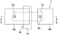
도 1은 본 발명에 따른 반도체 장치를 설명하기 위한 레이 아웃도이다.1 is a layout for explaining a semiconductor device according to the present invention.
본 발명의 반도체 장치는 박막 트랜지스터(T)와 캐패시터(Cst)가 일체형으로 형성된다. 박막 트랜지스터(T)는 반도체층(20), 반도체층(20)의 채널 영역 상부에 배치된 게이트 전극(40), 그리고 반도체층(20)의 소스 영역 및 드레인 영역에 연결된 소스 전극(60a) 및 드레인 전극(60b)으로 구성되며, 캐패시터(Cst)는 서로 중첩되도록 배치된 게이트 전극(40)과 소스 전극(60a) 또는 드레인 전극(60b)에 의해 구성된다.In the semiconductor device of the present invention, the thin film transistor T and the capacitor Cst are integrally formed. The thin film transistor T includes a
도 2는 도 1의 I1 - I2 부분을 절취한 단면도로서, 본 발명에 따른 반도체 장치를 보다 상세하게 설명하면 다음과 같다.FIG. 2 is a cross-sectional view taken along the line I1-I2 of FIG. 1, and the semiconductor device according to the present invention will be described in detail as follows.
도 1 및 도 2를 참조하면, 기판(10) 상에 반도체층(20)이 형성되고, 반도체층(20)을 포함하는 기판(10) 상에 게이트 절연층(30)이 형성된다.1 and 2, the
기판(10)은 실리콘(Si)이나 게르마늄(Ge)과 같은 반도체, 유리나 플라스틱과 같은 절연체 또는 금속 박막으로 이루어질 수 있고, 반도체층(20)은 비정질 실리콘, 결정질 실리콘 또는 화합물 반도체 등으로 형성될 수 있으며, 게이트 절연층(30)은 실리콘 산화물, 실리콘 질화물 또는 이들의 혼합물이나 적층 구조로 형성될 수 있다. 또한, 반도체층(20)이 형성되기 전에 기판(10) 상에 버퍼층(도시안됨)이 형성될 수 있다.The
반도체층(20) 상부의 게이트 절연층(30) 상에 게이트 전극(40)이 형성되고, 게이트 전극(40)을 포함하는 게이트 절연층(30) 상에 층간 절연층(50)이 형성된다.The
게이트 전극(40)은 금속이나 도핑된 반도체로 형성될 수 있으며, 층간 절연층(50)은 실리콘 산화물, 실리콘 질화물, 금속 산화물 또는 이들의 혼합물이나 적층 구조로 형성될 수 있다.The
층간 절연층(50) 상에는 반도체층(20)과 전기적으로 연결되도록 소스 및 드레인 전극(60a 및 60b)이 형성된다. 소스 및 드레인 전극(60a 및 60b)은 층간 절연층(40) 및 게이트 절연층(30)에 형성된 콘택홀(50a)을 통해 노출되는 반도체층(20)에 연결된다.Source and
이 때 소스 및 드레인 전극(60a 및 60b) 중 어느 하나의 전극 예를 들어, 소스 전극(60a)은 게이트 전극(40)의 적어도 일부와 중첩되도록 게이트 전극(40) 상부로 연장되며, 이에 의해 서로 중첩되도록 배치되는 소스 전극(60a), 층간 절연층(50) 및 게이트 전극(40)에 의해 캐패시터(Cst)가 형성된다. 즉, 게이트 전극(40)이 캐패시터(Cst)의 하나의 전극으로 이용되고, 게이트 전극(40) 상부로 연장된 소스 전극(60a)의 일부가 캐패시터(Cst)의 다른 하나의 전극으로 이용되며, 중첩되는 게이트 전극(40)과 소스 전극(60a) 사이의 층간 절연층(50)이 캐패시터(Cst)의 유전체로 이용된다.At this time, any one of the source and
도 1 및 도 2에는 소스 전극(60a)이 게이트 전극(40)의 일부와 중첩되도록 게이트 전극(40) 상부로 연장된 구조를 도시하였으나, 원하는 정전용량 및 드레인 전극(60b)과의 거리 등을 고려하여 중첩되는 정도를 결정할 수 있으며, 정전용량을 최대로 확보하기 위해서는 게이트 전극(40)의 전부와 중첩되도록 소스 전극(60a)을 형성하는 것이 바람직하다.
1 and 2 illustrate a structure in which the
상기와 같이 구성된 본 발명의 반도체 장치는 예를 들어, 평판표시장치의 화소회로에 적용될 수 있다.The semiconductor device of the present invention configured as described above can be applied to, for example, a pixel circuit of a flat panel display device.
도 3은 평판표시장치의 화소회로의 일 실시예로서, 두 개의 박막 트랜지스터(T1 및 T2), 하나의 저장 캐패시터(Cst) 및 발광소자(LED)로 이루어진 화소회로를 예로 들어 설명한다. 평판표시장치로는 액정표시장치(LCD), 유기전계발광 표시장치(OLED) 등이 적용될 수 있다.3 illustrates a pixel circuit including two thin film transistors T1 and T2, one storage capacitor Cst, and a light emitting device LED as an example of the pixel circuit of the flat panel display. As the flat panel display, a liquid crystal display (LCD), an organic light emitting display (OLED), or the like may be applied.
제 1 박막 트랜지스터(T1)는 스캔 라인(S) 및 데이터 라인(D)에 연결되어 스캔 신호에 따라 데이터 신호를 전달하는 스위칭 소자로서 동작된다. 이를 위해 게이트 전극을 통해 스캔 신호를 입력받고, 소스 전극을 통해 데이터 신호를 입력받는다.The first thin film transistor T1 is connected to the scan line S and the data line D and is operated as a switching element transferring a data signal according to the scan signal. To this end, a scan signal is input through the gate electrode and a data signal is input through the source electrode.
제 2 박막 트랜지스터(T2)는 전원전압(ELVDD) 및 발광소자(LED) 사이에 연결되어 상기 데이터 신호에 따라 발광소자(LED)를 동작시키는 구동 소자로서 동작된다. 또한, 저장 캐패시터(Cst)는 상기 데이터 신호에 해당하는 전압을 일정 시간동안 유지시키는 정전용량을 제공한다. 이를 위해 게이트 전극이 제 1 박막 트랜지스터(T1)의 드레인 전극에 연결되고, 소스 전극을 통해 전원전압(ELVDD)을 공급받으며, 드레인 전극이 발광소자(LED)에 연결된다.The second thin film transistor T2 is connected between the power supply voltage ELVDD and the light emitting device LED to operate as a driving device for operating the light emitting device LED according to the data signal. In addition, the storage capacitor Cst provides a capacitance for maintaining a voltage corresponding to the data signal for a predetermined time. To this end, the gate electrode is connected to the drain electrode of the first thin film transistor T1, the power supply voltage ELVDD is supplied through the source electrode, and the drain electrode is connected to the light emitting device LED.
도 2를 참조하면, 본 발명의 반도체 장치가 유기전계발광 표시장치(OLED)에 적용되는 경우, 발광소자(LED)는 애노드 전극(80), 유기 발광층(84) 및 캐소드 전극(86)을 포함하는 유기전계발광소자로 구성될 수 있다. 애노드 전극(80)은 제 2 박막 트랜지스터(T2)의 드레인 전극에 연결되고, 캐소드 전극(86)은 접지전압(ELVSS)에 연결된다.Referring to FIG. 2, when the semiconductor device of the present invention is applied to an organic light emitting display (OLED), the light emitting device (LED) includes an
애노드 전극(80)은 박막 트랜지스터(T)를 포함하는 상부에 형성된 평탄화층(70)의 비아홀을 통해 박막 트랜지스터(T)의 드레인 전극(60b)과 연결되며, 유기 발광층(84)은 화소 정의막(82)에 의해 노출되는 발광영역(개구부)의 애노드 전극(80) 상에 형성되고, 캐소드 전극(86)은 유기 발광층(84)을 포함하는 상부에 형성된다.The
상기와 같이 본 발명의 반도체 장치를 이용하면 저장 캐패시터(Cst)가 박막 트랜지스터(T)와 일체형으로 형성되기 때문에 별도로 저장 캐패시터를 형성하지 않아도 된다. 이는 저장 캐패시터(Cst)가 차지하는 면적을 감소시킬 수 있을 뿐만 아니라 발광소자(LED)의 개구율 즉, 발광영역의 크기를 증가시킬 수 있는 요인으로 작용하기 때문에 고집적 및 고화질의 평판표시장치를 용이하게 구현할 수 있다.As described above, when the semiconductor device of the present invention is used, since the storage capacitor Cst is formed integrally with the thin film transistor T, the storage capacitor does not need to be separately formed. This not only reduces the area occupied by the storage capacitor Cst but also increases the aperture ratio of the light emitting device LED, that is, the size of the light emitting area, so that a high density and high quality flat panel display device can be easily implemented. Can be.
저장 캐패시터(Cst)의 정전용량을 높게 확보하기 위해서는 스위칭 소자로 동작하는 제 1 박막 트랜지스터(T1)보다는 구동 소자로서 동작하는 제 2 박막 트랜지스터(T2)를 본 발명의 반도체 장치로 구성하는 것이 유리하다. 전류구동능력이 큰 구동 소자는 스위칭 소자에 비해 크기(폭 및 길이)가 크기 때문에 저장 캐패시터(Cst)의 정전용량을 높게 확보할 수 있다.In order to ensure a high capacitance of the storage capacitor Cst, it is advantageous to configure the second thin film transistor T2 acting as a driving element as the semiconductor device of the present invention rather than the first thin film transistor T1 acting as a switching element. . Since the driving device having a large current driving capability is larger in size (width and length) than the switching device, the capacitance of the storage capacitor Cst can be secured.
또한, 누설전류 문제로 인해 복수의 박막 트랜지스터를 직렬 또는 병렬로 연결하거나, 박막 트랜지스터를 다중 게이트 구조로 형성하는 경우 효과가 극대화될 수 있다.In addition, due to the leakage current problem, the effect may be maximized when the plurality of thin film transistors are connected in series or in parallel, or when the thin film transistors have a multi-gate structure.
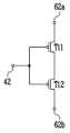
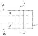
도 4a는 박막 트랜지스터(T11 및 T12)를 직렬로 연결한 구조로서, 도 4b와 같이 소스 전극(62a)과 게이트 전극(42)이 중첩되는 면적이 도 1의 구조에 비해 증가되기 때문에 저장 캐패시터(Cst)의 정전용량을 높게 확보할 수 있다. 설명되지 않은 부호 22는 반도체층을 도시한다.4A is a structure in which the thin film transistors T11 and T12 are connected in series. As shown in FIG. 4B, the overlapping area of the
도 5a는 박막 트랜지스터(T21 및 T22)를 병렬로 연결한 구조로서, 도 5b와 같이 소스 전극(64a)과 게이트 전극(44)이 중첩되는 면적이 도 1의 구조에 비해 증가되기 때문에 저장 캐패시터(Cst)의 정전용량을 높게 확보할 수 있다. 설명되지 않은 부호 24는 반도체층을 도시한다.5A illustrates a structure in which the thin film transistors T21 and T22 are connected in parallel. As shown in FIG. 5B, the overlapping area of the
도 6a는 온-전류(on-current)를 증가시키기 위해 다중 게이트 구조의 박막 트랜지스터(T31 및 T32)를 병렬로 연결한 구조로서, 도 6b와 같이 소스 전극(66a)과 게이트 전극(46)이 중첩되는 면적이 도 5b의 구조에 비해 더 증가되기 때문에 저장 캐패시터(Cst)의 정전용량을 높게 확보할 수 있다. 설명되지 않은 부호 26은 반도체층을 도시한다.FIG. 6A illustrates a structure in which thin-film transistors T31 and T32 having a multi-gate structure are connected in parallel to increase on-current. As shown in FIG. 6B, the
상기 실시예에서는 박막 트랜지스터(T)에 내장된 캐패시터(Cst)만을 설명하였으나, 정정용량을 증가시키기 위해 상기 캐패시터(Cst)와 인접하도록 다른 캐패시터(도시안됨)를 추가적으로 형성하고 상기 캐패시터(Cst)와 병렬로 연결할 수 있다.In the above embodiment, only the capacitor Cst embedded in the thin film transistor T has been described. However, in order to increase the capacitance, another capacitor (not shown) is additionally formed to be adjacent to the capacitor Cst, and the capacitor Cst Can be connected in parallel.
이상에서와 같이 상세한 설명과 도면을 통해 본 발명의 최적 실시예를 개시하였다. 용어들은 단지 본 발명을 설명하기 위한 목적에서 사용된 것이지 의미 한정이나 특허청구범위에 기재된 본 발명의 범위를 제한하기 위하여 사용된 것은 아니다. 그러므로 본 기술 분야의 통상의 지식을 가진 자라면 이로부터 다양한 변형 및 균등한 타 실시예가 가능하다는 점을 이해할 것이다. 따라서 본 발명의 진정한 기술적 보호 범위는 첨부된 특허청구범위의 기술적 사상에 의해 정해져야 할 것이다.
As described above, the optimal embodiment of the present invention has been disclosed through the detailed description and the drawings. It is to be understood that the terminology used herein is for the purpose of describing the present invention only and is not used to limit the scope of the present invention described in the claims or the claims. Therefore, those skilled in the art will appreciate that various modifications and equivalent embodiments are possible without departing from the scope of the present invention. Therefore, the true technical protection scope of the present invention will be defined by the technical spirit of the appended claims.
10: 기판
20, 22, 24, 26: 반도체층
30: 게이트 절연층
40, 42, 44, 46: 게이트 전극
50: 층간 절연층
50a: 콘택홀
60a, 62a, 64a, 66a: 소스 전극
60b, 62b, 64b, 66b: 드레인 전극
70: 평탄화층
80: 애노드 전극
82: 화소 정의막
84: 유기 발광층
86: 캐소드 전극10: substrate
20, 22, 24, 26: semiconductor layer
30: gate insulating layer
40, 42, 44, 46: gate electrode
50: interlayer insulation layer
50a: contact hole
60a, 62a, 64a, 66a: source electrode
60b, 62b, 64b, 66b: drain electrode
70: planarization layer
80: anode electrode
82: pixel defining layer
84: organic light emitting layer
86: cathode electrode
Claims (8)
Translated fromKorean게이트 절연층에 의해 상기 반도체층과 전기적으로 절연된 게이트 전극;
상기 게이트 전극을 포함하는 상기 게이트 절연층 상에 형성된 절연층; 및
상기 절연층 상에 상기 반도체층과 연결되도록 형성된 소스 전극 및 드레인 전극을 포함하며,
상기 소스 전극이 상기 게이트 전극의 적어도 일부와 중첩되도록 배치된 반도체 장치.A semiconductor layer formed on the substrate;
A gate electrode electrically insulated from the semiconductor layer by a gate insulating layer;
An insulating layer formed on the gate insulating layer including the gate electrode; And
A source electrode and a drain electrode formed to be connected to the semiconductor layer on the insulating layer,
And the source electrode overlapping at least a portion of the gate electrode.
상기 제 1 박막 트랜지스터에 연결된 제 2 박막 트랜지스터; 및
상기 제 2 박막 트랜지스터에 연결된 발광소자를 포함하며,
상기 제 2 박막 트랜지스터는 기판 상에 형성된 반도체층;
게이트 절연층에 의해 상기 반도체층과 전기적으로 절연된 게이트 전극;
상기 게이트 전극을 포함하는 상기 게이트 절연층 상에 형성된 절연층; 및
상기 절연층 상에 상기 반도체층과 연결되도록 형성된 소스 전극 및 드레인 전극을 포함하며,
상기 소스 전극이 상기 게이트 전극의 적어도 일부와 중첩되도록 배치된 평판표시장치.A first thin film transistor connected to the scan line and the data line;
A second thin film transistor connected to the first thin film transistor; And
A light emitting device connected to the second thin film transistor,
The second thin film transistor may include a semiconductor layer formed on a substrate;
A gate electrode electrically insulated from the semiconductor layer by a gate insulating layer;
An insulating layer formed on the gate insulating layer including the gate electrode; And
A source electrode and a drain electrode formed to be connected to the semiconductor layer on the insulating layer,
And a source electrode overlapping at least a portion of the gate electrode.
Priority Applications (6)
| Application Number | Priority Date | Filing Date | Title |
|---|---|---|---|
| KR1020120010388AKR20130089044A (en) | 2012-02-01 | 2012-02-01 | Semiconductor device and flat panel display device having the same |
| JP2012110492AJP6125155B2 (en) | 2012-02-01 | 2012-05-14 | Semiconductor device and flat panel display device including the same |
| US13/528,976US9053986B2 (en) | 2012-02-01 | 2012-06-21 | Semiconductor device and flat panel display including the same |
| CN201210311792.5ACN103247690B (en) | 2012-02-01 | 2012-08-29 | Semiconductor devices and the flat-panel monitor including the semiconductor devices |
| TW101131471ATWI603134B (en) | 2012-02-01 | 2012-08-30 | Semiconductor device and flat panel display therewith |
| EP12183869.2AEP2624299A1 (en) | 2012-02-01 | 2012-09-11 | Semiconductor device and flat panel display including the same |
Applications Claiming Priority (1)
| Application Number | Priority Date | Filing Date | Title |
|---|---|---|---|
| KR1020120010388AKR20130089044A (en) | 2012-02-01 | 2012-02-01 | Semiconductor device and flat panel display device having the same |
Publications (1)
| Publication Number | Publication Date |
|---|---|
| KR20130089044Atrue KR20130089044A (en) | 2013-08-09 |
Family
ID=46940315
Family Applications (1)
| Application Number | Title | Priority Date | Filing Date |
|---|---|---|---|
| KR1020120010388ACeasedKR20130089044A (en) | 2012-02-01 | 2012-02-01 | Semiconductor device and flat panel display device having the same |
Country Status (6)
| Country | Link |
|---|---|
| US (1) | US9053986B2 (en) |
| EP (1) | EP2624299A1 (en) |
| JP (1) | JP6125155B2 (en) |
| KR (1) | KR20130089044A (en) |
| CN (1) | CN103247690B (en) |
| TW (1) | TWI603134B (en) |
Families Citing this family (16)
| Publication number | Priority date | Publication date | Assignee | Title |
|---|---|---|---|---|
| KR101672091B1 (en)* | 2014-02-25 | 2016-11-02 | 엘지디스플레이 주식회사 | Organic emitting display device having multi-type thin film transistor |
| KR102354377B1 (en) | 2014-11-24 | 2022-01-21 | 삼성디스플레이 주식회사 | Organic light emitting diode display |
| KR102300026B1 (en)* | 2015-01-08 | 2021-09-09 | 삼성디스플레이 주식회사 | Display device |
| KR102328678B1 (en)* | 2015-02-09 | 2021-11-19 | 삼성디스플레이 주식회사 | Thin film transistor substrate, display apparatus comprising the same, method for manufacturing thin film transistor substrate, and method for manufacturing display apparatus |
| CN106373996B (en)* | 2015-07-21 | 2019-12-31 | 台达电子工业股份有限公司 | Semiconductor device |
| KR102430819B1 (en)* | 2015-08-19 | 2022-08-10 | 삼성디스플레이 주식회사 | Organic light emitting display apparatus and method for manufacturing the same |
| WO2017066601A1 (en) | 2015-10-16 | 2017-04-20 | Huang Yiren Ronnie | Method and apparatus for providing hybrid mode to access ssd drive |
| CN105185793A (en)* | 2015-10-28 | 2015-12-23 | 武汉华星光电技术有限公司 | Thin film transistor substrate and display device thereof |
| CN105552085B (en)* | 2015-12-25 | 2019-04-30 | 昆山国显光电有限公司 | A pixel driving circuit and its preparation method |
| CN105655347A (en)* | 2016-01-04 | 2016-06-08 | 昆山国显光电有限公司 | TFT backboard, preparation method thereof and display device |
| KR102483956B1 (en) | 2016-03-31 | 2023-01-03 | 삼성디스플레이 주식회사 | Display device |
| KR102824654B1 (en) | 2016-10-31 | 2025-06-23 | 엘지디스플레이 주식회사 | Organic light emitting diode display |
| KR102508468B1 (en)* | 2018-02-08 | 2023-03-10 | 삼성디스플레이 주식회사 | Display device |
| CN108320705B (en) | 2018-02-14 | 2021-04-27 | 京东方科技集团股份有限公司 | Pixel unit and its manufacturing method and array substrate |
| JP2019032557A (en)* | 2018-11-06 | 2019-02-28 | 株式会社ジャパンディスプレイ | Display device |
| KR102820506B1 (en)* | 2021-04-29 | 2025-06-17 | 삼성디스플레이 주식회사 | Display device and driving method of the same |
Family Cites Families (29)
| Publication number | Priority date | Publication date | Assignee | Title |
|---|---|---|---|---|
| JP2690067B2 (en) | 1991-06-14 | 1997-12-10 | シャープ株式会社 | Active matrix substrate |
| JPH0738118A (en)* | 1992-12-22 | 1995-02-07 | Korea Electron Telecommun | Method of manufacturing thin film transistor |
| JPH07302912A (en) | 1994-04-29 | 1995-11-14 | Semiconductor Energy Lab Co Ltd | Semiconductor device |
| CN1230919C (en)* | 1994-06-02 | 2005-12-07 | 株式会社半导体能源研究所 | Active Matrix Displays and Electro-Optic Components |
| JP3783786B2 (en)* | 1995-01-26 | 2006-06-07 | 株式会社半導体エネルギー研究所 | Active matrix display device |
| JP3329206B2 (en) | 1996-09-05 | 2002-09-30 | セイコーエプソン株式会社 | Color liquid crystal display device and pixel arrangement method |
| JP3784491B2 (en)* | 1997-03-28 | 2006-06-14 | 株式会社半導体エネルギー研究所 | Active matrix display device |
| US6680487B1 (en) | 1999-05-14 | 2004-01-20 | Semiconductor Energy Laboratory Co., Ltd. | Semiconductor comprising a TFT provided on a substrate having an insulating surface and method of fabricating the same |
| JP4307635B2 (en)* | 1999-06-22 | 2009-08-05 | 株式会社半導体エネルギー研究所 | Method for manufacturing semiconductor device |
| US7662677B2 (en)* | 2000-04-28 | 2010-02-16 | Semiconductor Energy Laboratory Co., Ltd. | Method of fabricating semiconductor device |
| JP4675005B2 (en)* | 2000-08-18 | 2011-04-20 | 株式会社半導体エネルギー研究所 | Light emitting device, electronic equipment |
| US6825496B2 (en) | 2001-01-17 | 2004-11-30 | Semiconductor Energy Laboratory Co., Ltd. | Light emitting device |
| JP4137454B2 (en)* | 2001-01-17 | 2008-08-20 | 株式会社半導体エネルギー研究所 | Light emitting device, electronic device, and method for manufacturing light emitting device |
| JP5025057B2 (en) | 2001-05-10 | 2012-09-12 | 株式会社半導体エネルギー研究所 | Method for manufacturing semiconductor device |
| KR100426031B1 (en) | 2001-12-29 | 2004-04-03 | 엘지.필립스 엘시디 주식회사 | an active matrix organic electroluminescence display and a manufacturing method of the same |
| CN101673508B (en)* | 2002-01-18 | 2013-01-09 | 株式会社半导体能源研究所 | Light-emitting device |
| JP3706107B2 (en)* | 2002-01-18 | 2005-10-12 | 株式会社半導体エネルギー研究所 | LIGHT EMITTING DEVICE AND ELECTRONIC DEVICE |
| KR20030069347A (en) | 2002-02-20 | 2003-08-27 | 일진다이아몬드(주) | Liquid crystal display and fabrication method thereof |
| US6847050B2 (en)* | 2002-03-15 | 2005-01-25 | Semiconductor Energy Laboratory Co., Ltd. | Semiconductor element and semiconductor device comprising the same |
| JP2003332578A (en)* | 2002-05-09 | 2003-11-21 | Sharp Corp | Thin film transistor, method of manufacturing the same, and liquid crystal display device using the same |
| KR100444030B1 (en)* | 2002-07-16 | 2004-08-12 | 엘지.필립스 엘시디 주식회사 | The organic electro-luminescence device |
| KR100611746B1 (en) | 2004-02-24 | 2006-08-10 | 삼성에스디아이 주식회사 | Noise-proof display |
| KR100699988B1 (en)* | 2004-03-19 | 2007-03-26 | 삼성에스디아이 주식회사 | Flat Panel Display |
| KR101107712B1 (en)* | 2005-02-28 | 2012-01-25 | 엘지디스플레이 주식회사 | LCD Display |
| JP2007005395A (en)* | 2005-06-21 | 2007-01-11 | Mitsubishi Electric Corp | Thin film transistor |
| US20070229408A1 (en)* | 2006-03-31 | 2007-10-04 | Eastman Kodak Company | Active matrix display device |
| WO2011064819A1 (en)* | 2009-11-27 | 2011-06-03 | パナソニック株式会社 | Light-emitting display device |
| KR101710179B1 (en)* | 2010-06-03 | 2017-02-27 | 삼성디스플레이 주식회사 | Flat panel display apparatus and manufacturing method of the same |
| KR101783352B1 (en)* | 2010-06-17 | 2017-10-10 | 삼성디스플레이 주식회사 | Flat panel display apparatus and manufacturing method of the same |
- 2012
- 2012-02-01KRKR1020120010388Apatent/KR20130089044A/ennot_activeCeased
- 2012-05-14JPJP2012110492Apatent/JP6125155B2/enactiveActive
- 2012-06-21USUS13/528,976patent/US9053986B2/enactiveActive
- 2012-08-29CNCN201210311792.5Apatent/CN103247690B/enactiveActive
- 2012-08-30TWTW101131471Apatent/TWI603134B/enactive
- 2012-09-11EPEP12183869.2Apatent/EP2624299A1/ennot_activeCeased
Also Published As
| Publication number | Publication date |
|---|---|
| JP2013162120A (en) | 2013-08-19 |
| CN103247690B (en) | 2017-12-19 |
| JP6125155B2 (en) | 2017-05-10 |
| US20130193439A1 (en) | 2013-08-01 |
| TW201333588A (en) | 2013-08-16 |
| US9053986B2 (en) | 2015-06-09 |
| TWI603134B (en) | 2017-10-21 |
| CN103247690A (en) | 2013-08-14 |
| EP2624299A1 (en) | 2013-08-07 |
Similar Documents
| Publication | Publication Date | Title |
|---|---|---|
| JP6125155B2 (en) | Semiconductor device and flat panel display device including the same | |
| US8212247B2 (en) | Organic light emitting display device and fabricating method thereof | |
| US8896044B1 (en) | Organic light emitting diode display | |
| CN107516471B (en) | Luminous panel | |
| US12148841B2 (en) | Thin film transistor array substrate and display device | |
| US8237168B2 (en) | Organic light emitting display device | |
| JP7623864B2 (en) | Thin Film Transistor Substrate | |
| JP2023547741A (en) | Display panels and electronic display devices | |
| US20170154941A1 (en) | Thin film transistor substrate for organic light-emitting diode display and manufacturing method thereof | |
| JP2011053711A (en) | Display device | |
| CN103227177A (en) | Pixel structure and thin film transistor | |
| US8669700B2 (en) | Organic light emitting diode display including source and drain electrodes separated from a gate electrode | |
| CN117096159A (en) | Display substrate, manufacturing method thereof and display device | |
| TWI703735B (en) | Semiconductor substrate, array substrate, inverter circuit, and switch circuit | |
| JP2007535164A (en) | Coplanar thin film transistor with additional source and drain insulation layers | |
| CN113013254A (en) | Thin film transistor, preparation method thereof and display panel | |
| CN110649003A (en) | Semiconductor substrate, array substrate, inverter circuit and switch circuit | |
| US12223886B2 (en) | Display apparatus including light emitting device and pixel driving circuit | |
| CN220829962U (en) | Array substrate and display device | |
| CN101887905B (en) | Image display system and manufacturing method thereof | |
| US20240237400A9 (en) | Display panel and manufacturing method thereof |
Legal Events
| Date | Code | Title | Description |
|---|---|---|---|
| PA0109 | Patent application | Patent event code:PA01091R01D Comment text:Patent Application Patent event date:20120201 | |
| N231 | Notification of change of applicant | ||
| PN2301 | Change of applicant | Patent event date:20120806 Comment text:Notification of Change of Applicant Patent event code:PN23011R01D | |
| PG1501 | Laying open of application | ||
| A201 | Request for examination | ||
| PA0201 | Request for examination | Patent event code:PA02012R01D Patent event date:20170201 Comment text:Request for Examination of Application Patent event code:PA02011R01I Patent event date:20120201 Comment text:Patent Application | |
| E902 | Notification of reason for refusal | ||
| PE0902 | Notice of grounds for rejection | Comment text:Notification of reason for refusal Patent event date:20180518 Patent event code:PE09021S01D | |
| AMND | Amendment | ||
| E601 | Decision to refuse application | ||
| PE0601 | Decision on rejection of patent | Patent event date:20181115 Comment text:Decision to Refuse Application Patent event code:PE06012S01D Patent event date:20180518 Comment text:Notification of reason for refusal Patent event code:PE06011S01I | |
| AMND | Amendment | ||
| PX0901 | Re-examination | Patent event code:PX09011S01I Patent event date:20181115 Comment text:Decision to Refuse Application Patent event code:PX09012R01I Patent event date:20180717 Comment text:Amendment to Specification, etc. | |
| E90F | Notification of reason for final refusal | ||
| PE0902 | Notice of grounds for rejection | Comment text:Final Notice of Reason for Refusal Patent event date:20190114 Patent event code:PE09021S02D | |
| PX0601 | Decision of rejection after re-examination | Comment text:Decision to Refuse Application Patent event code:PX06014S01D Patent event date:20190401 Comment text:Final Notice of Reason for Refusal Patent event code:PX06013S02I Patent event date:20190114 Comment text:Amendment to Specification, etc. Patent event code:PX06012R01I Patent event date:20181214 Comment text:Decision to Refuse Application Patent event code:PX06011S01I Patent event date:20181115 Comment text:Amendment to Specification, etc. Patent event code:PX06012R01I Patent event date:20180717 Comment text:Notification of reason for refusal Patent event code:PX06013S01I Patent event date:20180518 |