KR20130086807A - Graphene device and method of manufacturing the same - Google Patents
Graphene device and method of manufacturing the sameDownload PDFInfo
- Publication number
- KR20130086807A KR20130086807AKR20120007797AKR20120007797AKR20130086807AKR 20130086807 AKR20130086807 AKR 20130086807AKR 20120007797 AKR20120007797 AKR 20120007797AKR 20120007797 AKR20120007797 AKR 20120007797AKR 20130086807 AKR20130086807 AKR 20130086807A
- Authority
- KR
- South Korea
- Prior art keywords
- substrate
- layer
- graphene
- insulating layer
- gate
- Prior art date
- Legal status (The legal status is an assumption and is not a legal conclusion. Google has not performed a legal analysis and makes no representation as to the accuracy of the status listed.)
- Granted
Links
Images


Classifications
- H—ELECTRICITY
- H10—SEMICONDUCTOR DEVICES; ELECTRIC SOLID-STATE DEVICES NOT OTHERWISE PROVIDED FOR
- H10D—INORGANIC ELECTRIC SEMICONDUCTOR DEVICES
- H10D30/00—Field-effect transistors [FET]
- H10D30/40—FETs having zero-dimensional [0D], one-dimensional [1D] or two-dimensional [2D] charge carrier gas channels
- H10D30/47—FETs having zero-dimensional [0D], one-dimensional [1D] or two-dimensional [2D] charge carrier gas channels having 2D charge carrier gas channels, e.g. nanoribbon FETs or high electron mobility transistors [HEMT]
- H—ELECTRICITY
- H01—ELECTRIC ELEMENTS
- H01L—SEMICONDUCTOR DEVICES NOT COVERED BY CLASS H10
- H01L21/00—Processes or apparatus adapted for the manufacture or treatment of semiconductor or solid state devices or of parts thereof
- H01L21/67—Apparatus specially adapted for handling semiconductor or electric solid state devices during manufacture or treatment thereof; Apparatus specially adapted for handling wafers during manufacture or treatment of semiconductor or electric solid state devices or components ; Apparatus not specifically provided for elsewhere
- H01L21/683—Apparatus specially adapted for handling semiconductor or electric solid state devices during manufacture or treatment thereof; Apparatus specially adapted for handling wafers during manufacture or treatment of semiconductor or electric solid state devices or components ; Apparatus not specifically provided for elsewhere for supporting or gripping
- H01L21/6835—Apparatus specially adapted for handling semiconductor or electric solid state devices during manufacture or treatment thereof; Apparatus specially adapted for handling wafers during manufacture or treatment of semiconductor or electric solid state devices or components ; Apparatus not specifically provided for elsewhere for supporting or gripping using temporarily an auxiliary support
- H—ELECTRICITY
- H10—SEMICONDUCTOR DEVICES; ELECTRIC SOLID-STATE DEVICES NOT OTHERWISE PROVIDED FOR
- H10D—INORGANIC ELECTRIC SEMICONDUCTOR DEVICES
- H10D30/00—Field-effect transistors [FET]
- H10D30/40—FETs having zero-dimensional [0D], one-dimensional [1D] or two-dimensional [2D] charge carrier gas channels
- H10D30/47—FETs having zero-dimensional [0D], one-dimensional [1D] or two-dimensional [2D] charge carrier gas channels having 2D charge carrier gas channels, e.g. nanoribbon FETs or high electron mobility transistors [HEMT]
- H10D30/481—FETs having two-dimensional material channels, e.g. transition metal dichalcogenide [TMD] FETs
- H—ELECTRICITY
- H10—SEMICONDUCTOR DEVICES; ELECTRIC SOLID-STATE DEVICES NOT OTHERWISE PROVIDED FOR
- H10D—INORGANIC ELECTRIC SEMICONDUCTOR DEVICES
- H10D62/00—Semiconductor bodies, or regions thereof, of devices having potential barriers
- H10D62/80—Semiconductor bodies, or regions thereof, of devices having potential barriers characterised by the materials
- H10D62/881—Semiconductor bodies, or regions thereof, of devices having potential barriers characterised by the materials being a two-dimensional material
- H10D62/882—Graphene
- H—ELECTRICITY
- H10—SEMICONDUCTOR DEVICES; ELECTRIC SOLID-STATE DEVICES NOT OTHERWISE PROVIDED FOR
- H10D—INORGANIC ELECTRIC SEMICONDUCTOR DEVICES
- H10D64/00—Electrodes of devices having potential barriers
- H10D64/20—Electrodes characterised by their shapes, relative sizes or dispositions
- H10D64/23—Electrodes carrying the current to be rectified, amplified, oscillated or switched, e.g. sources, drains, anodes or cathodes
- H10D64/251—Source or drain electrodes for field-effect devices
- H10D64/258—Source or drain electrodes for field-effect devices characterised by the relative positions of the source or drain electrodes with respect to the gate electrode
- H—ELECTRICITY
- H01—ELECTRIC ELEMENTS
- H01L—SEMICONDUCTOR DEVICES NOT COVERED BY CLASS H10
- H01L2221/00—Processes or apparatus adapted for the manufacture or treatment of semiconductor or solid state devices or of parts thereof covered by H01L21/00
- H01L2221/67—Apparatus for handling semiconductor or electric solid state devices during manufacture or treatment thereof; Apparatus for handling wafers during manufacture or treatment of semiconductor or electric solid state devices or components; Apparatus not specifically provided for elsewhere
- H01L2221/683—Apparatus for handling semiconductor or electric solid state devices during manufacture or treatment thereof; Apparatus for handling wafers during manufacture or treatment of semiconductor or electric solid state devices or components; Apparatus not specifically provided for elsewhere for supporting or gripping
- H01L2221/68304—Apparatus for handling semiconductor or electric solid state devices during manufacture or treatment thereof; Apparatus for handling wafers during manufacture or treatment of semiconductor or electric solid state devices or components; Apparatus not specifically provided for elsewhere for supporting or gripping using temporarily an auxiliary support
- H01L2221/68327—Apparatus for handling semiconductor or electric solid state devices during manufacture or treatment thereof; Apparatus for handling wafers during manufacture or treatment of semiconductor or electric solid state devices or components; Apparatus not specifically provided for elsewhere for supporting or gripping using temporarily an auxiliary support used during dicing or grinding
- H—ELECTRICITY
- H01—ELECTRIC ELEMENTS
- H01L—SEMICONDUCTOR DEVICES NOT COVERED BY CLASS H10
- H01L2221/00—Processes or apparatus adapted for the manufacture or treatment of semiconductor or solid state devices or of parts thereof covered by H01L21/00
- H01L2221/67—Apparatus for handling semiconductor or electric solid state devices during manufacture or treatment thereof; Apparatus for handling wafers during manufacture or treatment of semiconductor or electric solid state devices or components; Apparatus not specifically provided for elsewhere
- H01L2221/683—Apparatus for handling semiconductor or electric solid state devices during manufacture or treatment thereof; Apparatus for handling wafers during manufacture or treatment of semiconductor or electric solid state devices or components; Apparatus not specifically provided for elsewhere for supporting or gripping
- H01L2221/68304—Apparatus for handling semiconductor or electric solid state devices during manufacture or treatment thereof; Apparatus for handling wafers during manufacture or treatment of semiconductor or electric solid state devices or components; Apparatus not specifically provided for elsewhere for supporting or gripping using temporarily an auxiliary support
- H01L2221/6835—Apparatus for handling semiconductor or electric solid state devices during manufacture or treatment thereof; Apparatus for handling wafers during manufacture or treatment of semiconductor or electric solid state devices or components; Apparatus not specifically provided for elsewhere for supporting or gripping using temporarily an auxiliary support used as a support during build up manufacturing of active devices
- H—ELECTRICITY
- H01—ELECTRIC ELEMENTS
- H01L—SEMICONDUCTOR DEVICES NOT COVERED BY CLASS H10
- H01L2221/00—Processes or apparatus adapted for the manufacture or treatment of semiconductor or solid state devices or of parts thereof covered by H01L21/00
- H01L2221/67—Apparatus for handling semiconductor or electric solid state devices during manufacture or treatment thereof; Apparatus for handling wafers during manufacture or treatment of semiconductor or electric solid state devices or components; Apparatus not specifically provided for elsewhere
- H01L2221/683—Apparatus for handling semiconductor or electric solid state devices during manufacture or treatment thereof; Apparatus for handling wafers during manufacture or treatment of semiconductor or electric solid state devices or components; Apparatus not specifically provided for elsewhere for supporting or gripping
- H01L2221/68304—Apparatus for handling semiconductor or electric solid state devices during manufacture or treatment thereof; Apparatus for handling wafers during manufacture or treatment of semiconductor or electric solid state devices or components; Apparatus not specifically provided for elsewhere for supporting or gripping using temporarily an auxiliary support
- H01L2221/68368—Apparatus for handling semiconductor or electric solid state devices during manufacture or treatment thereof; Apparatus for handling wafers during manufacture or treatment of semiconductor or electric solid state devices or components; Apparatus not specifically provided for elsewhere for supporting or gripping using temporarily an auxiliary support used in a transfer process involving at least two transfer steps, i.e. including an intermediate handle substrate
- Y—GENERAL TAGGING OF NEW TECHNOLOGICAL DEVELOPMENTS; GENERAL TAGGING OF CROSS-SECTIONAL TECHNOLOGIES SPANNING OVER SEVERAL SECTIONS OF THE IPC; TECHNICAL SUBJECTS COVERED BY FORMER USPC CROSS-REFERENCE ART COLLECTIONS [XRACs] AND DIGESTS
- Y10—TECHNICAL SUBJECTS COVERED BY FORMER USPC
- Y10S—TECHNICAL SUBJECTS COVERED BY FORMER USPC CROSS-REFERENCE ART COLLECTIONS [XRACs] AND DIGESTS
- Y10S977/00—Nanotechnology
- Y10S977/70—Nanostructure
- Y10S977/734—Fullerenes, i.e. graphene-based structures, such as nanohorns, nanococoons, nanoscrolls or fullerene-like structures, e.g. WS2 or MoS2 chalcogenide nanotubes, planar C3N4, etc.
Landscapes
- Engineering & Computer Science (AREA)
- Physics & Mathematics (AREA)
- Condensed Matter Physics & Semiconductors (AREA)
- General Physics & Mathematics (AREA)
- Manufacturing & Machinery (AREA)
- Computer Hardware Design (AREA)
- Microelectronics & Electronic Packaging (AREA)
- Power Engineering (AREA)
- Thin Film Transistor (AREA)
- Carbon And Carbon Compounds (AREA)
Abstract
Translated fromKoreanDescription
Translated fromKorean그래핀 소자 및 그 제조방법에 관한 것이다.It relates to a graphene device and a method of manufacturing the same.
실리콘(Si) 기반의 반도체 소자는 지금까지 빠른 속도로 고집적화 및 고성능화되어 왔다. 하지만 Si 물질의 특성 한계와 제조공정의 한계 등으로 인해, 향후 수년 후부터는, Si 기반의 반도체 소자를 더 이상 고집적화 및 고성능화시키는 것은 어려울 것이라 예상되고 있다.Silicon (Si) based semiconductor devices have been rapidly integrated and high performance. However, due to the limitations of the characteristics of the Si material and the limitations of the manufacturing process, it is expected that in the next few years, it will be difficult to further integrate and improve the performance of Si-based semiconductor devices.
이에, Si 기반의 반도체 소자의 한계를 뛰어넘을 수 있는 차세대 소자에 대한 연구가 진행되고 있다. 예컨대, 그래핀(graphene)과 같은 탄소 기반의 나노구조체를 적용하여 우수한 성능의 소자를 제조하려는 시도가 이루어지고 있다. 그래핀은 탄소 원자들로 이루어진 육방정계(hexagonal) 단층 구조물로서, 구조적/화학적으로 안정하고, 전기적/물리적으로 우수한 특성을 나타낼 수 있다. 예를 들어, 그래핀은 Si 보다 100배 이상 빠른 전하 이동도(∼2×10⁵㎠/Vs)를 갖고, 구리(Cu)보다 100배 이상 큰 전류 밀도(약 108A/㎠)를 갖는다. 이러한 그래핀은 기존 소자의 한계를 극복할 수 있는 차세대 소재로 주목받고 있다.Therefore, research on the next generation devices capable of surpassing the limits of Si-based semiconductor devices is being conducted. For example, attempts have been made to fabricate high performance devices using carbon-based nanostructures such as graphene. Graphene is a hexagonal monolayer structure composed of carbon atoms, and is structurally / chemically stable and may exhibit excellent electrical / physical properties. For example, graphene has a charge mobility (˜2 × 105 cm 2 / Vs) at least 100 times faster than Si, and a current density (about 108 A / cm 2) at least 100 times higher than copper (Cu). . Such graphene is attracting attention as a next generation material that can overcome the limitation of existing devices.
그러나 그래핀 형성 공정상의 제약으로 인해, 그래핀을 적용한 전자 소자의 제조는 현실적으로 용이하지 않다. 현재의 기술로는 절연 박막 위에 양질의 그래핀을 성장시키는 것이 어렵기 때문에, 금속 박막 위에 그래핀을 형성한 후, 이를 다른 기판으로 전이(transfer) 시켜 소자를 제조하는 것이 일반적이다. 그런데 이와 같이 그래핀을 전이하는 과정에서 결함이 발생하거나 오염 물질에 노출될 수 있으며, 그래핀의 취급(handling)이 용이하지 않은 문제가 있다. 따라서 그래핀을 적용한 소자의 구현에 제약이 따른다.However, due to the constraints on the graphene forming process, manufacturing of electronic devices using graphene is not practically easy. Since it is difficult to grow high quality graphene on an insulating thin film with current technology, it is common to manufacture a device by forming graphene on a metal thin film and then transferring it to another substrate. However, defects may be generated or exposed to contaminants in the process of transferring graphenes, and handling of graphene is not easy. Therefore, there is a limitation in the implementation of the device to apply the graphene.
우수한 성능의 그래핀 소자 및 이를 제조하는 방법을 제공한다.It provides a graphene device of excellent performance and a method of manufacturing the same.
그래핀의 손상 및 오염을 방지(또는 최소화)할 수 있는 그래핀 소자의 제조방법을 제공한다.Provided is a method of manufacturing a graphene device capable of preventing (or minimizing) damage and contamination of graphene.
본 발명의 일 측면(aspect)에 따르면, 제1 기판 상에 그래핀층을 형성하는 단계; 상기 제1 기판 상에 상기 그래핀층을 포함하는 소자부를 형성하는 단계; 상기 제1 기판의 상기 소자부 측에 제2 기판을 부착하는 단계; 및 상기 제1 기판을 제거하는 단계;를 포함하는 그래핀 소자의 제조방법이 제공된다.According to an aspect of the invention, forming a graphene layer on the first substrate; Forming an element part including the graphene layer on the first substrate; Attaching a second substrate to the element portion side of the first substrate; And removing the first substrate.
상기 소자부를 형성하는 단계는 상기 그래핀층의 제1 영역 및 제2 영역에 각각 접촉된 소오스전극 및 드레인전극을 형성하는 단계를 포함할 수 있다.The forming of the device unit may include forming a source electrode and a drain electrode in contact with the first region and the second region of the graphene layer, respectively.
상기 소자부를 형성하는 단계는 상기 그래핀층, 소오스전극 및 드레인전극을 덮는 게이트절연층을 형성하는 단계; 및 상기 소오스전극과 드레인전극 사이의 상기 게이트절연층 상에 게이트를 형성하는 단계;를 더 포함할 수 있다.The forming of the device unit may include forming a gate insulating layer covering the graphene layer, the source electrode, and the drain electrode; And forming a gate on the gate insulating layer between the source electrode and the drain electrode.
상기 소자부와 상기 제2 기판 사이에 상기 소자부를 덮는 절연층을 형성하는 단계; 및 상기 절연층 및 게이트절연층의 일부를 식각하여 상기 소오스전극, 드레인전극 및 게이트를 노출시키는 단계;를 더 포함할 수 있다.Forming an insulating layer covering the device portion between the device portion and the second substrate; And etching the portions of the insulating layer and the gate insulating layer to expose the source electrode, the drain electrode, and the gate.
상기 제1 기판을 제거하는 단계 후, 상기 소자부에 제3 기판을 부착하는 단계를 더 포함할 수 있다. 이때, 상기 제2 기판과 상기 제3 기판 사이에 상기 소자부가 배치될 수 있다.After removing the first substrate, the method may further include attaching a third substrate to the device portion. In this case, the device portion may be disposed between the second substrate and the third substrate.
상기 소자부에 상기 제3 기판을 부착하는 경우, 상기 제2 기판을 제거하는 단계를 더 포함할 수 있다.When attaching the third substrate to the device portion, the method may further include removing the second substrate.
상기 제3 기판은 유리 기판, 플라스틱 기판 또는 폴리머 기판일 수 있다.The third substrate may be a glass substrate, a plastic substrate, or a polymer substrate.
상기 제3 기판은 플렉서블(flexible) 기판일 수 있다.The third substrate may be a flexible substrate.
상기 소자부와 제3 기판 사이에 보호층을 형성하는 단계를 더 포함할 수 있다.The method may further include forming a protective layer between the device portion and the third substrate.
상기 제1 기판을 제거하는 단계 후, 상기 소자부를 덮는 절연층을 형성하는 단계를 포함할 수 있다. 이때, 상기 절연층과 상기 제2 기판 사이에 상기 소자부가 배치될 수 있다.After removing the first substrate, the method may include forming an insulating layer covering the device portion. In this case, the device portion may be disposed between the insulating layer and the second substrate.
상기 소오스전극, 드레인전극 및 게이트는 각각 제1 패드부, 제2 패드부 및 제3 패드부를 포함하도록 형성될 수 있고, 상기 절연층은 상기 제1 내지 제3 패드부를 덮도록 형성될 수 있으며, 상기 절연층의 일부를 식각하여 상기 제1 내지 제3 패드부를 노출시키는 단계를 더 수행할 수 있다.The source electrode, the drain electrode, and the gate may be formed to include a first pad part, a second pad part, and a third pad part, respectively, and the insulating layer may be formed to cover the first to third pad parts. A portion of the insulating layer may be etched to expose the first to third pad parts.
상기 제1 기판을 제거하는 단계 후, 상기 그래핀층, 소오스전극 및 드레인전극을 덮는 게이트절연층을 형성하는 단계; 및 상기 소오스전극과 드레인전극 사이의 상기 게이트절연층 상에 게이트를 형성하는 단계;를 포함할 수 있다.After removing the first substrate, forming a gate insulating layer covering the graphene layer, the source electrode, and the drain electrode; And forming a gate on the gate insulating layer between the source electrode and the drain electrode.
상기 소오스전극 및 드레인전극은 각각 제1 패드부 및 제2 패드부 포함하도록 형성될 수 있고, 상기 게이트절연층의 일부를 식각하여 상기 제1 및 제2 패드부를 노출시키는 단계를 더 수행할 수 있다.The source electrode and the drain electrode may be formed to include a first pad part and a second pad part, respectively, and a portion of the gate insulating layer may be etched to expose the first and second pad parts. .
상기 제1 기판과 상기 그래핀층 사이에 촉매층을 형성하는 단계를 더 포함할 수 있다.The method may further include forming a catalyst layer between the first substrate and the graphene layer.
상기 제1 기판과 상기 촉매층 사이에 중간층을 형성하는 단계를 더 포함할 수 있다.The method may further include forming an intermediate layer between the first substrate and the catalyst layer.
상기 제1 기판을 제거하는 단계는 상기 촉매층을 식각하는 단계를 포함할 수 있다.Removing the first substrate may include etching the catalyst layer.
상기 제1 기판을 제거하는 단계는 상기 촉매층 또는 상기 중간층을 식각하는 단계를 포함할 수 있다.Removing the first substrate may include etching the catalyst layer or the intermediate layer.
상기 제2 기판을 부착하는 단계 전, 상기 제1 기판 상에 상기 소자부를 덮는 보호층을 형성하는 단계를 더 수행할 수 있다.Prior to attaching the second substrate, the forming of the protective layer covering the device portion on the first substrate may be further performed.
상기 제2 기판은, 예컨대, 폴리머 기판일 수 있다.The second substrate may be, for example, a polymer substrate.
상기 제1 기판 상에 상기 소자부를 복수 개 포함하는 소자층을 형성하는 단계; 및 상기 소자층을 패터닝하여 상기 복수의 소자부를 분리하는 단계;를 포함할 수 있다.Forming a device layer including a plurality of device parts on the first substrate; And separating the plurality of device parts by patterning the device layer.
상기 제1 기판과 상기 소자층 사이에 희생층이 더 구비될 수 있다.A sacrificial layer may be further provided between the first substrate and the device layer.
상기 제1 기판을 제거하는 단계는 상기 복수의 소자부 사이로 식각 용액을 주입하여 상기 희생층을 식각하는 단계를 포함할 수 있다.Removing the first substrate may include etching the sacrificial layer by injecting an etching solution between the plurality of device portions.
상기 희생층은 금속층 또는 절연층으로 형성할 수 있다.The sacrificial layer may be formed of a metal layer or an insulating layer.
본 발명의 다른 측면에 따르면, 기판 상에 구비된 것으로, 표면에 오목한 영역을 갖는 제1 절연층; 상기 제1 절연층의 오목한 영역에 구비된 그래핀 소자부; 및 상기 그래핀 소자부를 덮도록 구비된 제2 절연층;을 포함하고, 상기 그래핀 소자부는 게이트; 상기 게이트를 덮도록 구비된 게이트절연층; 상기 게이트 양측의 상기 게이트절연층 상에 구비된 소오스전극 및 드레인전극; 그리고 상기 소오스전극 및 드레인전극에 접촉하도록 구비된 그래핀층;을 포함하는 그래핀 트랜지스터가 제공된다.According to another aspect of the invention, provided on the substrate, the first insulating layer having a concave region on the surface; A graphene element unit provided in the concave region of the first insulating layer; And a second insulating layer provided to cover the graphene device unit, wherein the graphene device unit comprises: a gate; A gate insulating layer provided to cover the gate; Source and drain electrodes provided on the gate insulating layers on both sides of the gate; And a graphene layer provided to contact the source electrode and the drain electrode.
상기 게이트절연층은 상기 그래핀층 양측의 상기 제1 절연층 위로 연장된 구조를 가질 수 있다.The gate insulating layer may have a structure extending over the first insulating layer on both sides of the graphene layer.
상기 제1 절연층 위로 연장된 상기 게이트절연층 부분은 상기 그래핀층과 동일한 높이에 구비될 수 있다.The gate insulation layer portion extending over the first insulation layer may be provided at the same height as the graphene layer.
상기 게이트는 상기 소오스전극 및 드레인전극과 오버랩(overlap)된 구조를 가질 수 있다.The gate may have a structure overlapping with the source electrode and the drain electrode.
상기 기판은, 예컨대, 폴리머 기판일 수 있다.The substrate may be, for example, a polymer substrate.
본 발명의 다른 측면에 따르면, 기판 상에 구비된 보호층; 상기 보호층 내에 구비된 소오스전극 및 드레인전극; 상기 소오스전극과 드레인전극을 연결하도록 구비되고, 상기 보호층의 상면과 동일한 높이로 구비된 그래핀층; 상기 보호층 상에 상기 그래핀층을 덮도록 구비된 게이트절연층; 및 상기 게이트절연층 상에 구비된 게이트;를 포함하는 그래핀 트랜지스터가 제공된다.According to another aspect of the invention, the protective layer provided on the substrate; A source electrode and a drain electrode provided in the protective layer; A graphene layer provided to connect the source electrode and the drain electrode, and having the same height as the upper surface of the protective layer; A gate insulating layer provided on the protective layer to cover the graphene layer; And a gate provided on the gate insulating layer.
상기 그래핀층의 상면과 그 주위의 상기 보호층의 상면은 동일한 높이를 가질 수 있다.An upper surface of the graphene layer and an upper surface of the protective layer around the graphene layer may have the same height.
상기 소오스전극은 상기 그래핀층의 제1 영역 아래에 구비될 수 있고, 상기 드레인전극은 상기 그래핀층의 제2 영역 아래에 구비될 수 있다.The source electrode may be provided under the first region of the graphene layer, and the drain electrode may be provided under the second region of the graphene layer.
상기 기판은, 예컨대, 폴리머 기판일 수 있다.The substrate may be, for example, a polymer substrate.
그래핀의 손상 및 오염이 최소화 또는 방지된 우수한 성능의 그래핀 소자를 구현할 수 있다.High performance graphene devices can be implemented with minimized or prevented damage and contamination of graphene.
소오스/드레인전극에 대해서 게이트의 위치가 자기 정렬(self-align) 되어 소오스/드레인전극 간 저항이 최소화된 그래핀 소자를 구현할 수 있다.The gate positions are self-aligned with respect to the source / drain electrodes, thereby realizing a graphene device having a minimum resistance between the source and drain electrodes.
다양한 기판을 적용할 수 있어서, 적용 분야 확장에 유리한 그래핀 소자를 구현할 수 있다.Various substrates may be applied, thereby realizing a graphene device that is advantageous for expanding an application field.
웨이퍼 스케일(wafer scale)에서 복수의 그래핀 소자를 용이하게 제조할 수 있다.A plurality of graphene devices can be easily manufactured on a wafer scale.
도 1a 내지 도 1l은 본 발명의 실시예에 따른 그래핀 소자의 제조방법을 보여주는 단면도이다.
도 2a 내지 도 2d는 도 1b의 구조를 형성하는 방법을 예시적으로 보여주는 단면도이다.
도 3a 내지 도 3d는 본 발명의 다른 실시예에 따른 그래핀 소자의 제조방법을 보여주는 단면도이다.
도 3c는 본 발명의 실시예에 따른 그래핀 소자를 보여주는 단면도이다.
도 4a는 도 3c의 평면 구조를 예시적으로 보여주는 평면도이다.
도 4b는 도 3d의 평면 구조를 예시적으로 보여주는 평면도이다.
도 5는 도 4a의 변형예를 보여주는 평면도이다.
도 6a 내지 도 6d는 본 발명의 다른 실시예에 따른 그래핀 소자의 제조방법을 보여주는 단면도이다.
도 6c는 본 발명의 다른 실시예에 따른 그래핀 소자를 보여주는 단면도이다.
도 7a는 도 6c의 평면 구조를 예시적으로 보여주는 평면도이다.
도 7b는 도 6d의 평면 구조를 예시적으로 보여주는 평면도이다.
도 8a 내지 도 8e는 본 발명의 다른 실시예에 따른 그래핀 소자의 제조방법을 보여주는 단면도이다.1A to 1L are cross-sectional views illustrating a method of manufacturing a graphene device according to an embodiment of the present invention.
2A through 2D are cross-sectional views illustrating a method of forming the structure of FIG. 1B.
3A to 3D are cross-sectional views illustrating a method of manufacturing a graphene device according to another exemplary embodiment of the present invention.
3C is a cross-sectional view illustrating a graphene device according to an exemplary embodiment of the present invention.
4A is a plan view illustrating the planar structure of FIG. 3C.
4B is a plan view illustrating the planar structure of FIG. 3D.
5 is a plan view illustrating a modification of FIG. 4A.
6A through 6D are cross-sectional views illustrating a method of manufacturing a graphene device according to another exemplary embodiment of the present invention.
6C is a cross-sectional view illustrating a graphene device according to another exemplary embodiment of the present invention.
FIG. 7A is a plan view illustrating the planar structure of FIG. 6C.
FIG. 7B is a plan view illustrating the planar structure of FIG. 6D.
8A to 8E are cross-sectional views illustrating a method of manufacturing a graphene device according to another exemplary embodiment of the present invention.
이하, 본 발명의 실시예에 따른 그래핀 소자 및 그 제조방법을 첨부된 도면을 참조하여 상세하게 설명한다. 첨부된 도면에 도시된 층이나 영역들의 폭 및 두께는 명세서의 명확성을 위해 다소 과장되게 도시된 것이다. 상세한 설명 전체에 걸쳐 동일한 참조번호는 동일한 구성요소를 나타낸다.Hereinafter, a graphene device and a method of manufacturing the same according to an embodiment of the present invention will be described in detail with reference to the accompanying drawings. The width and thickness of the layers or regions shown in the accompanying drawings are somewhat exaggerated for clarity. Like numbers refer to like elements throughout.
도 1a 내지 도 1l은 본 발명의 실시예에 따른 그래핀 소자의 제조방법을 보여주는 단면도이다.1A to 1L are cross-sectional views illustrating a method of manufacturing a graphene device according to an embodiment of the present invention.
도 1a를 참조하면, 제1 기판(SUB1) 상에 촉매층(CT1)을 형성할 수 있다. 제1 기판(SUB1)으로는, 예컨대, 실리콘 기판을 사용할 수 있다. 촉매층(CT1)을 형성하기 전에, 제1 기판(SUB1) 상에 소정의 중간층(N1)을 먼저 형성한 후, 중간층(N1) 상에 촉매층(CT1)을 형성할 수 있다. 중간층(N1)은 기판(SUB1)과 촉매층(CT1) 사이의 반응, 예컨대, 실리사이드 반응을 방지하는 역할을 할 수 있다. 또한 중간층(N1)은 제1 기판(SUB1)과 촉매층(CT1) 사이의 물질 확산을 방지하는 역할을 할 수 있다. 중간층(N1)은 절연층, 예컨대, 실리콘 산화물층으로 형성할 수 있다. 제1 기판(SUB1)이 실리콘 기판인 경우, 제1 기판(SUB1)의 표면부(상면부)를 산화시켜 중간층(N1)으로 사용되는 실리콘 산화물층을 형성할 수 있다. 중간층(N1)의 두께는 100∼300㎚ 정도일 수 있다. 중간층(N1)의 물질 및 형성방법은 전술한 바에 한정되지 않고, 다양하게 변화될 수 있다. 예컨대, 중간층(N1)은 질화물로 형성될 수 있고, 산화 공정이 아닌 다른 방법으로 형성될 수 있다. 경우에 따라서는, 중간층(N1)을 형성하지 않을 수도 있다.Referring to FIG. 1A, the catalyst layer CT1 may be formed on the first substrate SUB1. As the first substrate SUB1, for example, a silicon substrate can be used. Before forming the catalyst layer CT1, a predetermined intermediate layer N1 may be first formed on the first substrate SUB1, and then the catalyst layer CT1 may be formed on the intermediate layer N1. The intermediate layer N1 may serve to prevent a reaction between the substrate SUB1 and the catalyst layer CT1, for example, a silicide reaction. In addition, the intermediate layer N1 may serve to prevent material diffusion between the first substrate SUB1 and the catalyst layer CT1. The intermediate layer N1 may be formed of an insulating layer, for example, a silicon oxide layer. When the first substrate SUB1 is a silicon substrate, the silicon oxide layer used as the intermediate layer N1 may be formed by oxidizing the surface portion (upper surface portion) of the first substrate SUB1. The thickness of the intermediate layer N1 may be about 100 to 300 nm. The material and the method of forming the intermediate layer N1 are not limited to the above, and may be variously changed. For example, the intermediate layer N1 may be formed of nitride and may be formed by a method other than an oxidation process. In some cases, the intermediate layer N1 may not be formed.
촉매층(CT1)은 Ni, Cu, Co, Pt, Ru 등으로 이루어진 금속 및 이들의 혼합물 중 적어도 하나로 형성할 수 있다. 촉매층(CT1)은 단층 또는 다층 구조를 가질 수 있다. 촉매층(CT1)은 도금(plating), 증발(evaporation), 스퍼터링(sputtering), CVD(chemical vapor deposition), ALD(atomic layer deposition) 등 다양한 방법으로 형성할 수 있다. 촉매층(CT1)은 대략 100∼500㎚ 정도의 두께로 형성할 수 있다.The catalyst layer CT1 may be formed of at least one of a metal made of Ni, Cu, Co, Pt, Ru, and the like and a mixture thereof. The catalyst layer CT1 may have a single layer or a multilayer structure. The catalyst layer CT1 may be formed by various methods, such as plating, evaporation, sputtering, chemical vapor deposition (CVD), and atomic layer deposition (ALD). The catalyst layer CT1 can be formed to a thickness of about 100 to 500 nm.
다음, 촉매층(CT1) 상에 그래핀층(GP1)을 형성할 수 있다. 그래핀층(GP1)은 CVD나 열분해(pyrolysis) 법 등으로 형성할 수 있다. 그래핀층(GP1)을 CVD로 형성하는 경우, 촉매층(CT1) 상에 탄소를 포함하는 소오스 가스를 흘려주는데, 상기 소오스 가스로는 CH4, C2H2, C2H4, CO 등을 사용할 수 있다. 그래핀층(GP1)을 형성하기 위해서는 700∼1100℃ 정도의 고온 공정이 요구될 수 있다. 따라서 제1 기판(SUB1)은 상기 고온 공정을 견딜 수 있는 물질로 구성될 필요가 있다. 이런 점에서, 제1 기판(SUB1)으로 실리콘 기판을 사용할 수 있다. 그러나 실리콘 기판 이외에도 고온 공정을 견딜 수 있는 기판이면 어느 기판이든 제1 기판(SUB1)으로 사용할 수 있다. 예컨대, 석영(quartz) 기판을 제1 기판(SUB1)으로 사용할 수 있다. 경우에 따라서는, SiC 기판을 제1 기판(SUB1)으로 사용할 수도 있다. SiC 기판을 제1 기판(SUB1)으로 사용하는 경우, 촉매층(CT1) 없이 SiC 기판 위에 직접 그래핀층(GP1)을 형성할 수 있다.Next, the graphene layer GP1 may be formed on the catalyst layer CT1. The graphene layer GP1 may be formed by CVD or pyrolysis. When the graphene layer GP1 is formed by CVD, a source gas containing carbon is flowed on the catalyst layer CT1, and as the source gas, CH4 , C2 H2 , C2 H4 , CO, or the like may be used. have. In order to form the graphene layer GP1, a high temperature process of about 700 to 1100 ° C. may be required. Therefore, the first substrate SUB1 needs to be made of a material that can withstand the high temperature process. In this regard, a silicon substrate may be used as the first substrate SUB1. However, in addition to the silicon substrate, any substrate may be used as the first substrate SUB1 as long as the substrate can withstand a high temperature process. For example, a quartz substrate may be used as the first substrate SUB1. In some cases, a SiC substrate may be used as the first substrate SUB1. When the SiC substrate is used as the first substrate SUB1, the graphene layer GP1 may be directly formed on the SiC substrate without the catalyst layer CT1.
도 1b를 참조하면, 그래핀층(GP1)을 소정 형태로 패터닝한 상태에서, 그래핀층(GP1)의 제1 영역 및 제2 영역에 각각 접촉된 소오스전극(S1) 및 드레인전극(D1)을 형성할 수 있다. 소오스전극(S1) 및 드레인전극(D1)은 각각 그래핀층(GP1)의 일단 및 타단에 구비될 수 있다. 소오스전극(S1)과 드레인전극(D1) 사이의 그래핀층(GP1) 영역을 '채널영역'이라 할 수 있다. 도 1b와 같은 그래핀층(GP1)과 소오스전극(S1) 및 드레인전극(D1)을 형성하는 방법은 다양할 수 있다. 예컨대, 제1 마스크 공정으로 도 1a의 그래핀층(GP1)을 먼저 패터닝한 후에, 제2 마스크 공정으로 소오스/드레인용 도전층을 패터닝하여 소오스전극(S1) 및 드레인전극(D1)을 형성할 수 있다. 또는 도 1a의 그래핀층(GP1) 상에 소오스/드레인용 도전층을 형성한 후, 그래핀층(GP1)과 상기 소오스/드레인용 도전층을 하나의 마스크로 함께 패터닝(1차 패터닝)한 다음, 다른 마스크를 사용해서 상기 소오스/드레인용 도전층을 패터닝(2차 패터닝)할 수 있다. 상기 1차 패터닝에 의해 도 1b와 같은 그래핀층(GP1)이 얻어질 수 있고, 상기 1차 및 2차 패터닝에 의해 소오스전극(S1) 및 드레인전극(D1)이 얻어질 수 있다. 또는 도 1a의 그래핀층(GP1)을 도 1b의 형태로 패터닝한 후에, 리프트-오프(lift-off) 방법을 사용해서 소오스전극(S1) 및 드레인전극(D1)을 형성할 수도 있다.Referring to FIG. 1B, the source electrode S1 and the drain electrode D1 are formed in contact with the first and second regions of the graphene layer GP1 while the graphene layer GP1 is patterned in a predetermined shape. can do. The source electrode S1 and the drain electrode D1 may be provided at one end and the other end of the graphene layer GP1, respectively. The graphene layer GP1 region between the source electrode S1 and the drain electrode D1 may be referred to as a 'channel region'. The method of forming the graphene layer GP1, the source electrode S1, and the drain electrode D1 as shown in FIG. 1B may be various. For example, after the graphene layer GP1 of FIG. 1A is first patterned by the first mask process, the source / drain conductive layer may be patterned by the second mask process to form the source electrode S1 and the drain electrode D1. have. Alternatively, after the source / drain conductive layer is formed on the graphene layer GP1 of FIG. 1A, the graphene layer GP1 and the source / drain conductive layer are patterned together as a mask (primary patterning). The source / drain conductive layer can be patterned (secondary patterned) using another mask. The graphene layer GP1 as shown in FIG. 1B may be obtained by the first patterning, and the source electrode S1 and the drain electrode D1 may be obtained by the first and second patterning. Alternatively, after the graphene layer GP1 of FIG. 1A is patterned in the form of FIG. 1B, the source electrode S1 and the drain electrode D1 may be formed using a lift-off method.
이하에서는, 도 1b의 구조를 형성하기 위한 다양한 방법 중 하나를 도 2a 내지 도 2d를 참조하여 예시적으로 설명한다.Hereinafter, one of various methods for forming the structure of FIG. 1B will be described by way of example with reference to FIGS. 2A to 2D.
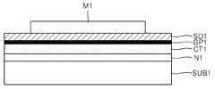
도 2a를 참조하면, 도 1a의 그래핀층(GP1) 상에 소오스/드레인용 도전층(SD1)을 형성할 수 있고, 소오스/드레인용 도전층(SD1) 상에 제1 마스크패턴(M1)을 형성할 수 있다.Referring to FIG. 2A, the source / drain conductive layer SD1 may be formed on the graphene layer GP1 of FIG. 1A, and the first mask pattern M1 may be formed on the source / drain conductive layer SD1. Can be formed.
도 2b를 참조하면, 제1 마스크패턴(M1)을 식각 장벽으로 이용해서 소오스/드레인용 도전층(SD1) 및 그래핀층(GP1)을 순차로 식각할 수 있다. 따라서 소오스/드레인용 도전층(SD1)과 그래핀층(GP1)은 위에서 보았을 때, 동일한 모양으로 패터닝될 수 있다.Referring to FIG. 2B, the source / drain conductive layer SD1 and the graphene layer GP1 may be sequentially etched using the first mask pattern M1 as an etch barrier. Therefore, the source / drain conductive layer SD1 and the graphene layer GP1 may be patterned in the same shape when viewed from above.
도 2c를 참조하면, 제1 마스크패턴(M1)을 제거한 다음, 소오스/드레인용 도전층(SD1) 상에 제2 마스크패턴(M2)을 형성할 수 있다. 제2 마스크패턴(M2)은 소오스전극 및 드레인전극을 형성하기 위한 식각 마스크이다.Referring to FIG. 2C, after removing the first mask pattern M1, the second mask pattern M2 may be formed on the source / drain conductive layer SD1. The second mask pattern M2 is an etching mask for forming the source electrode and the drain electrode.
도 2d를 참조하면, 제2 마스크패턴(M2)을 식각 장벽으로 이용해서 소오스/드레인용 도전층(SD1)을 식각할 수 있다. 그 결과, 소오스전극(S1) 및 드레인전극(D1)이 형성될 수 있다. 이후, 제2 마스크패턴(M2)을 제거하면, 도 1b의 구조가 얻어질 수 있다.Referring to FIG. 2D, the source / drain conductive layer SD1 may be etched using the second mask pattern M2 as an etch barrier. As a result, the source electrode S1 and the drain electrode D1 can be formed. Thereafter, when the second mask pattern M2 is removed, the structure of FIG. 1B may be obtained.
소오스전극(S1) 및 드레인전극(D1)을 형성하기 위한 도전층, 즉, 상기 소오스/드레인용 도전층(SD1)은, 예컨대, 증발(evaporation) 법을 사용해서 형성할 수 있다. 그래핀층(GP1)은 플라즈마에 의해 손상될 수 있기 때문에, 소오스/드레인용 도전층(SD1)은 플라즈마를 사용하지 않는 공정으로 형성할 수 있다. 그 일례가 상기 증발(evaporation) 법이다. 그러나 소오스/드레인용 도전층(SD1)의 형성방법은 증발 법으로 한정되지 않고, 다양하게 변화될 수 있다. 또한 소오스/드레인용 도전층(SD1)을 패터닝(식각) 할 때에도 플라즈마를 사용하지 않는 공정, 예컨대, 습식 식각(wet etch) 공정을 사용할 수 있다. 또는 리프트-오프(lift-off) 공정을 사용해서 서로 이격된 소오스전극(S1) 및 드레인전극(D1)을 직접 형성할 수도 있다.The conductive layer for forming the source electrode S1 and the drain electrode D1, that is, the source / drain conductive layer SD1 can be formed using, for example, an evaporation method. Since the graphene layer GP1 may be damaged by the plasma, the source / drain conductive layer SD1 may be formed by a process not using plasma. One example is the evaporation method. However, the method of forming the source / drain conductive layer SD1 is not limited to the evaporation method, and may be variously changed. In addition, even when patterning (etching) the source / drain conductive layer SD1, a process using no plasma may be used, for example, a wet etch process. Alternatively, the source electrode S1 and the drain electrode D1 spaced apart from each other may be directly formed by using a lift-off process.
다시 도 1b를 참조하면, 소오스전극(S1) 및 드레인전극(D1)은 그래핀층(GP1)과 전기적으로 오믹 콘택(ohmic contact) 할 수 있는 물질로 형성할 수 있다. 예컨대, 소오스전극(S1) 및 드레인전극(D1)은 Au, Cu, Ni, Ti, Pt, Ru, Pd 등으로 구성된 금속 및 이들의 조합 중에서 선택된 물질로 형성할 수 있다. 구체적인 예로, 소오스전극(S1) 및 드레인전극(D1)은 Ti/Au, Pd/Au 등으로 형성할 수 있다. 경우에 따라서는, 소오스전극(S1) 및 드레인전극(D1)과 그래핀층(GP1) 사이에 오믹 콘택층(미도시)을 더 형성할 수 있다. 이 경우, 그래핀층(GP1)과 오믹 콘택되지 않는 물질이라도 소오스전극(S1) 및 드레인전극(D1) 물질로 적용할 수 있다.Referring again to FIG. 1B, the source electrode S1 and the drain electrode D1 may be formed of a material capable of electrically ohmic contact with the graphene layer GP1. For example, the source electrode S1 and the drain electrode D1 may be formed of a material selected from a metal consisting of Au, Cu, Ni, Ti, Pt, Ru, Pd, or a combination thereof. As a specific example, the source electrode S1 and the drain electrode D1 may be formed of Ti / Au, Pd / Au, or the like. In some cases, an ohmic contact layer (not shown) may be further formed between the source electrode S1, the drain electrode D1, and the graphene layer GP1. In this case, a material that is not in ohmic contact with the graphene layer GP1 may be used as the source electrode S1 and the drain electrode D1.
도 1c를 참조하면, 촉매층(CT1) 상에 그래핀층(GP1), 소오스전극(S1) 및 드레인전극(D1)을 덮는 게이트절연층(GI1)을 형성할 수 있다. 게이트절연층(GI1)은 Si 산화물, Si 질화물, Si 질산화물 등으로 형성하거나, Si 질화물보다 유전율이 높은 고유전(high-k) 물질, 예컨대, Al 산화물, Hf 산화물 등으로 형성하거나, 폴리머와 같은 유기물로 형성할 수도 있다. 또는 위에 언급된 물질들 중에서 적어도 두 개를 조합하여 게이트절연층(GI1)을 형성할 수도 있다. 게이트절연층(GI1)은 열(thermal) ALD, 열(thermal) CVD, 증발(evaporation) 법 등으로 형성할 수 있다. 게이트절연층(GI1) 형성시, 공정 온도는 약 400℃ 이하일 수 있지만, 경우에 따라서는 400℃ 이상일 수도 있다. 게이트절연층(GI1)의 두께는, 예컨대, 10∼30㎚ 정도일 수 있다.Referring to FIG. 1C, a gate insulating layer GI1 may be formed on the catalyst layer CT1 to cover the graphene layer GP1, the source electrode S1, and the drain electrode D1. The gate insulating layer GI1 may be formed of Si oxide, Si nitride, Si nitride, or the like, or may be formed of a high-k material having a higher dielectric constant than Si nitride, such as Al oxide, Hf oxide, or the like. It can also be formed from organic matter. Alternatively, at least two of the above materials may be combined to form the gate insulating layer GI1. The gate insulating layer GI1 may be formed by thermal ALD, thermal CVD, evaporation, or the like. When the gate insulating layer GI1 is formed, the process temperature may be about 400 ° C. or less, but in some cases, may be 400 ° C. or more. The thickness of the gate insulating layer GI1 may be, for example, about 10 to 30 nm.
다음, 소오스전극(S1)과 드레인전극(D1) 사이의 게이트절연층(GI1) 상에 게이트(G1)를 형성할 수 있다. 게이트(G1)는 소오스전극(S1) 및 드레인전극(D1) 위로 어느 정도 연장된 구조를 가질 수 있다. 즉, 게이트(G1)는 소오스전극(S1) 및 드레인전극(D1)과 어느 정도 오버랩(overlap)된 구조를 가질 수 있다. 그러나 경우에 따라서는, 게이트(G1)가 소오스전극(S1) 및 드레인전극(D1)과 오버랩되지 않을 수도 있다. 또한 도 1c에서는 게이트(G1)의 높이가 게이트절연층(GI1)보다 높은 경우가 도시되어 있지만, 게이트(G1)의 높이는 게이트절연층(GI1)의 높이와 동일하거나 유사할 수도 있다. 여기서, 게이트절연층(GI1)의 높이는 소오스전극(S1) 및 드레인전극(D1) 상에 형성된 게이트절연층(GI1)의 높이를 의미한다. 게이트(G1)는 일반적인 반도체 소자에서 사용하는 도전 물질(금속, 도전성 산화물 등)로 형성될 수 있다. 이와 같이, 게이트(G1)를 형성하면, 소오스전극(S1) 및 드레인전극(D1)에 대한 게이트(G1)의 위치가 자기 정렬(self-align) 되는 효과를 얻을 수 있다. 소오스전극(S1)과 드레인전극(D1) 사이의 공간에 게이트(G1)를 매립하기 때문에, 소오스전극(S1) 및 드레인전극(D1)에 대한 게이트(G1)의 위치가 자동 정렬될 수 있다. 또한, 게이트(G1)가 소오스전극(S1) 및 드레인전극(D1)과 오버랩(overlap)된 구조를 가질 때, 게이트(G1)가 다소 오정렬(misalign) 되더라도, 유효한(effective) 게이트 영역의 위치는 변하지 않고 일정하게 유지될 수 있다. 상기 유효한 게이트 영역은 소오스전극(S1)과 드레인전극(D1) 사이의 게이트(G1) 영역이다. 이와 같이, 본 실시예에서는 소오스전극(S1) 및 드레인전극(D1)에 대한 게이트(G1)의 위치가 자기 정렬되기 때문에, 오정렬 문제를 방지(또는 억제)할 수 있고, 소오스/드레인전극(S1, D1) 사이의 저항을 최소화하는 효과를 얻을 수 있다.Next, a gate G1 may be formed on the gate insulating layer GI1 between the source electrode S1 and the drain electrode D1. The gate G1 may have a structure extending to some extent over the source electrode S1 and the drain electrode D1. That is, the gate G1 may have a structure overlapping with the source electrode S1 and the drain electrode D1 to some extent. However, in some cases, the gate G1 may not overlap the source electrode S1 and the drain electrode D1. In addition, although the height of the gate G1 is higher than the gate insulating layer GI1 in FIG. 1C, the height of the gate G1 may be the same as or similar to the height of the gate insulating layer GI1. Here, the height of the gate insulating layer GI1 refers to the height of the gate insulating layer GI1 formed on the source electrode S1 and the drain electrode D1. The gate G1 may be formed of a conductive material (metal, conductive oxide, etc.) used in a general semiconductor device. As such, when the gate G1 is formed, the position of the gate G1 with respect to the source electrode S1 and the drain electrode D1 is self-aligned. Since the gate G1 is buried in the space between the source electrode S1 and the drain electrode D1, the position of the gate G1 with respect to the source electrode S1 and the drain electrode D1 can be automatically aligned. In addition, when the gate G1 has a structure overlapped with the source electrode S1 and the drain electrode D1, even if the gate G1 is slightly misaligned, the position of the effective gate region is It can remain constant without change. The effective gate region is a gate G1 region between the source electrode S1 and the drain electrode D1. As described above, in this embodiment, since the positions of the gates G1 with respect to the source electrode S1 and the drain electrode D1 are self-aligned, misalignment problems can be prevented (or suppressed), and the source / drain electrodes S1 can be prevented. , The effect of minimizing the resistance between D1) can be obtained.
도 1d를 참조하면, 제1 기판(SUB1) 상에 게이트절연층(GI1) 및 게이트(G1)를 덮는 절연층(IL1)을 형성할 수 있다. 절연층(IL1)은, 예컨대, Si 산화물, Si 질화물, Si 질산화물 등으로 형성할 수 있다. 절연층(IL1)의 두께는, 예컨대, 100∼500㎚ 정도일 수 있다.Referring to FIG. 1D, an insulating layer IL1 covering the gate insulating layer GI1 and the gate G1 may be formed on the first substrate SUB1. The insulating layer IL1 can be formed of Si oxide, Si nitride, Si nitride oxide, or the like, for example. The thickness of the insulating layer IL1 may be, for example, about 100 to 500 nm.
도 1e를 참조하면, 절연층(IL1) 및 게이트절연층(GI1)을 부분적으로 식각하여 게이트(G1), 소오스전극(S1) 및 드레인전극(D1) 각각의 일부를 노출시킬 수 있다. 이렇게 게이트(G1), 소오스전극(S1) 및 드레인전극(D1)의 일부를 노출시키는 오픈(open) 공정의 시점은 달라질 수 있다. 예컨대, 상기 오픈 공정은 본 제조방법의 마지막 단계에서 수행할 수도 있다.Referring to FIG. 1E, a portion of the gate G1, the source electrode S1, and the drain electrode D1 may be exposed by partially etching the insulating layer IL1 and the gate insulating layer GI1. The timing of the open process exposing a part of the gate G1, the source electrode S1, and the drain electrode D1 may be different. For example, the open process may be performed at the last step of the manufacturing method.
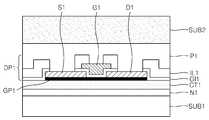
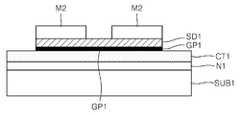
도 1a 내지 도 1e의 방법으로 제1 기판(SUB1) 상에 그래핀층(GP1)을 포함하는 소자부(device portion)(DP1)를 형성한 것으로 볼 수 있다. 상기 소자부(DP1)는 '그래핀 트랜지스터'일 수 있다.It can be seen that the device portion DP1 including the graphene layer GP1 is formed on the first substrate SUB1 by the method of FIGS. 1A to 1E. The device portion DP1 may be a graphene transistor.
도 1f를 참조하면, 제1 기판(SUB1) 상에 소자부(DP1)를 덮는 제1 보호층(P1)을 형성할 수 있다. 제1 보호층(P1)은 폴리머 물질이나 SOG(spin on glass) 물질로 형성할 수 있고, 예컨대, 스핀 코팅법으로 형성할 수 있다. 제1 보호층(P1)은 평탄한 표면을 갖도록 형성될 수 있다. 제1 보호층(P1)의 표면이 평탄하지 않은 경우, 그 표면을 평탄화하는 공정을 추가적으로 수행할 수도 있다. 이러한 제1 보호층(P1)은 후속 공정에서 제2 기판(도 1g의 SUB2)의 부착을 용이하게 하기 위해 형성하는 층일 수 있다. 또한 제1 보호층(P1)은 추후에 제1 기판(SUB1)을 제거하는 단계에서 소자부(DP1)를 보호하는 역할을 할 수 있다.Referring to FIG. 1F, a first passivation layer P1 covering the device portion DP1 may be formed on the first substrate SUB1. The first protective layer P1 may be formed of a polymer material or a spin on glass (SOG) material, for example, by a spin coating method. The first passivation layer P1 may be formed to have a flat surface. When the surface of the first passivation layer P1 is not flat, a process of planarizing the surface may be additionally performed. The first protective layer P1 may be a layer formed to facilitate the attachment of the second substrate (SUB2 of FIG. 1G) in a subsequent process. In addition, the first passivation layer P1 may serve to protect the device portion DP1 in a later step of removing the first substrate SUB1.
도 1g를 참조하면, 제1 보호층(P1) 상에 제2 기판(SUB2)을 부착할 수 있다. 제2 기판(SUB2)은 소자부(DP1) 및 제1 보호층(P1)을 사이에 두고 제1 기판(SUB1) 상에 부착된 것으로 볼 수 있다. 제2 기판(SUB2)은, 예컨대, 폴리머를 포함하는 기판일 수 있다. 구체적인 예로, 제2 기판(SUB2)은 접착성 테이프(adhesive tape)일 수 있다. 상기 접착성 테이프는 자외선(ultraviolet ray)(UV ray)에 의해 접착력이 약해지는 자외선 릴리즈 타입(UV release type)이거나, 열에 의해 접착력이 약해지는 서멀 릴리즈 타입(thermal release type)일 수 있다. 또는 제2 기판(SUB2)은 소정의 용매에 의해 제거 가능한 폴리머로 형성될 수 있다. 그러나 제2 기판(SUB2)의 물질은 접착성 테이프와 같은 폴리머로 한정되지 않고, 다양하게 변화될 수 있다. 경우에 따라서는, 제2 기판(SUB2)을 유리(glass)나 실리콘(Si)으로 형성할 수도 있다. 이 경우, 제1 보호층(P1)과 제2 기판(SUB2) 사이에 소정의 접착층(미도시)을 더 구비시킬 수도 있다. 제2 기판(SUB2)은 추후에 제1 기판(SUB1)을 분리하는 단계 및 그 후속 단계에서 소자부(DP1)가 구겨지거나 접히는 것을 방지하는 역할을 할 수 있다. 경우에 따라서는, 제1 보호층(P1) 자체가 제2 기판(SUB2)의 역할을 대신할 수도 있다. 이 경우, 제1 보호층(P1)을 기판으로 여길 수 있고, 제2 기판(SUB2)을 사용하지 않을 수 있다.Referring to FIG. 1G, a second substrate SUB2 may be attached onto the first passivation layer P1. The second substrate SUB2 may be regarded as being attached to the first substrate SUB1 with the device portion DP1 and the first protective layer P1 interposed therebetween. The second substrate SUB2 may be, for example, a substrate including a polymer. As a specific example, the second substrate SUB2 may be an adhesive tape. The adhesive tape may be an ultraviolet release type in which the adhesive strength is weakened by ultraviolet rays or a thermal release type in which the adhesive strength is weakened by heat. Alternatively, the second substrate SUB2 may be formed of a polymer removable by a predetermined solvent. However, the material of the second substrate SUB2 is not limited to a polymer such as an adhesive tape, and may be variously changed. In some cases, the second substrate SUB2 may be formed of glass or silicon (Si). In this case, a predetermined adhesive layer (not shown) may be further provided between the first protective layer P1 and the second substrate SUB2. The second substrate SUB2 may serve to prevent the element portion DP1 from being wrinkled or folded in a later step of separating the first substrate SUB1 and subsequent steps thereof. In some cases, the first protective layer P1 itself may take the role of the second substrate SUB2. In this case, the first protective layer P1 may be regarded as a substrate, and the second substrate SUB2 may not be used.
도 1h를 참조하면, 제1 기판(SUB1)을 제거/분리할 수 있다. 제1 기판(SUB1)은 촉매층(CT1)이나 중간층(N1)을 식각함으로써 제거/분리될 수 있다. 본 실시예에서는 촉매층(CT1)을 식각하여 제1 기판(SUB1)을 제거/분리하는 경우가 도시되어 있다. 촉매층(CT1)의 식각에는, 예컨대, FeCl3나 HNO3 등과 같은 금속 에천트(etchant)가 사용될 수 있다. 만약, 촉매층(CT1)이 아닌 중간층(N1)을 식각하여 제1 기판(SUB1)을 제거하는 경우에는, 중간층(N1)의 식각을 위해, 예컨대, HF가 함유된 식각액을 사용할 수 있다. 제1 기판(SUB1)의 제거/분리 공정은 전술한 바에 한정되지 않고, 다양하게 변형될 수 있다. 예컨대, 제1 기판(SUB1)의 대부분을 연마 공정으로 제거한 후, 잔류된 제1 기판(SUB1)을 소정의 식각액으로 제거한 다음, 중간층(N1)과 촉매층(CT1)을 연속적으로 제거할 수 있다. 상기 잔류된 제1 기판(SUB1)을 제거하기 위한 식각액으로는 KOH, TMAH(tetramethylammonium hydroxide) 등을 사용할 수 있다.Referring to FIG. 1H, the first substrate SUB1 may be removed / separated. The first substrate SUB1 may be removed / separated by etching the catalyst layer CT1 or the intermediate layer N1. In this embodiment, a case where the first substrate SUB1 is removed / separated by etching the catalyst layer CT1 is illustrated. For etching the catalyst layer CT1, for example, a metal etchant such as FeCl3 or HNO3 may be used. When the first substrate SUB1 is removed by etching the intermediate layer N1 rather than the catalyst layer CT1, an etchant containing HF may be used for etching the intermediate layer N1. The removal / separation process of the first substrate SUB1 is not limited to the above description and may be variously modified. For example, after removing most of the first substrate SUB1 by a polishing process, the remaining first substrate SUB1 may be removed with a predetermined etching solution, and then the intermediate layer N1 and the catalyst layer CT1 may be continuously removed. As an etching solution for removing the remaining first substrate SUB1, KOH, tetramethylammonium hydroxide (TMAH), or the like may be used.
도 1i를 참조하면, 제1 기판(SUB1)이 제거되어 노출된 소자부(DP1)의 하면에 제2 보호층(P2)을 형성할 수 있다. 제2 보호층(P2)은 그래핀층(GP1)의 물성/특성이 변하지 않도록 그래핀층(GP1)을 보호하는 역할을 할 수 있다. 예컨대, 제2 보호층(P2)은 Si 산화물, Si 질화물, Si 질산화물 등으로 형성하거나, Al 산화물 및 Hf 산화물과 같은 고유전 물질로 형성하거나, 폴리머로 형성할 수도 있다. 제2 보호층(P2)은 그래핀층(GP1)에 손상을 주지 않는 방법, 예컨대, 열(thermal) ALD, 열(thermal) CVD, 증발(evaporation) 법 등으로 형성할 수 있다. 도 1i에서는 소자부(DP1)의 하면에 제2 보호층(P2)을 형성하는 것으로 도시하였지만, 실제로는, 제2 기판(SUB2)과 소자부(DP1)를 포함하는 구조물을 위·아래로 뒤집은 상태에서, 즉, 소자부(DP1)의 그래핀층(GP1)이 위쪽으로 향하도록 한 후, 제2 보호층(P2)을 형성할 수 있다.Referring to FIG. 1I, a second passivation layer P2 may be formed on the bottom surface of the device portion DP1 exposed by removing the first substrate SUB1. The second protective layer P2 may serve to protect the graphene layer GP1 so that the physical properties / characteristics of the graphene layer GP1 do not change. For example, the second protective layer P2 may be formed of Si oxide, Si nitride, Si nitride oxide, or the like, or may be formed of a high dielectric material such as Al oxide and Hf oxide, or may be formed of a polymer. The second passivation layer P2 may be formed by a method that does not damage the graphene layer GP1, for example, thermal ALD, thermal CVD, evaporation, or the like. In FIG. 1I, the second protective layer P2 is formed on the lower surface of the element portion DP1, but in reality, the structure including the second substrate SUB2 and the element portion DP1 is turned upside down. In the state, that is, the graphene layer GP1 of the element portion DP1 is directed upward, and the second protective layer P2 may be formed.
도 1j를 참조하면, 제2 보호층(P2)에 제3 기판(SUB3)을 부착할 수 있다. 제3 기판(SUB3)은 제2 보호층(P2)을 사이에 두고 소자부(DP1)에 부착된 것이라 할 수 있다. 제3 기판(SUB3)과 제2 기판(SUB2) 사이에 소자부(DP1)가 구비될 수 있다. 제3 기판(SUB3)은, 예컨대, 유리 기판이나 플라스틱 기판 또는 폴리머 기판일 수 있다. 제3 기판(SUB3)은 플렉서블(flexible) 기판일 수 있지만, 단단한(rigid) 기판일 수도 있다. 제3 기판(SUB3)의 선택에는 공정 온도 등에 의한 제약이 없기 때문에, 필요에 따라 다양한 기판을 제3 기판(SUB3)으로 적용할 수 있다.Referring to FIG. 1J, the third substrate SUB3 may be attached to the second protective layer P2. The third substrate SUB3 may be attached to the element portion DP1 with the second protective layer P2 interposed therebetween. An element portion DP1 may be provided between the third substrate SUB3 and the second substrate SUB2. The third substrate SUB3 may be, for example, a glass substrate, a plastic substrate, or a polymer substrate. The third substrate SUB3 may be a flexible substrate, but may also be a rigid substrate. Since the selection of the third substrate SUB3 is not limited by the process temperature, various substrates can be applied to the third substrate SUB3 as necessary.
도 1k를 참조하면, 제2 기판(SUB2)을 제거할 수 있다. 예컨대, 제2 기판(SUB2)이 서멀 릴리즈 타입(thermal release type)의 접착성 테이프인 경우, 약 200℃ 정도의 열을 가함으로써, 제2 기판(SUB2)을 용이하게 제거할 수 있다. 제2 기판(SUB2)의 타입에 따라, 그 제거 방법은 달라질 수 있다.Referring to FIG. 1K, the second substrate SUB2 may be removed. For example, when the second substrate SUB2 is a thermal release type adhesive tape, the second substrate SUB2 may be easily removed by applying heat of about 200 ° C. Depending on the type of the second substrate SUB2, the removal method may vary.
다음, 제1 보호층(P1)을 제거할 수 있다. 제1 보호층(P1)은 산소 플라즈마 공정이나 습식 식각 공정으로 제거할 수 있다. 제1 보호층(P1)이 폴리머인 경우, 산소 플라즈마 공정으로 제거할 수 있고, 제1 보호층(P1)이 유전층인 경우, 습식 식각 공정으로 제거할 수 있다. 제1 보호층(P1)이 제거된 결과물이 도 1l에 도시되어 있다. 도 1l을 참조하면, 제3 기판(SUB3) 상에 그래핀층(GP1)을 포함하는 소자부(DP1)가 구비될 수 있다.Next, the first protective layer P1 may be removed. The first passivation layer P1 may be removed by an oxygen plasma process or a wet etching process. When the first protective layer P1 is a polymer, it may be removed by an oxygen plasma process, and when the first protective layer P1 is a dielectric layer, it may be removed by a wet etching process. The result of removing the first protective layer P1 is shown in FIG. 1L. Referring to FIG. 1L, an element portion DP1 including a graphene layer GP1 may be provided on the third substrate SUB3.
이와 같이, 본 실시예에서는 제1 기판(SUB1) 상에서 그래핀층(GP1)을 포함하는 소자부(DP1)를 제조한 후, 이를 다른 기판(즉, 제3 기판(SUB3))에 부착할 수 있다. 이 과정에서 취급성을 위해 소자부(DP1)를 지지하는 제2 기판(SUB2)이 임시로 사용될 수 있고, 제1 기판(SUB1)이 제거될 수 있다. 다시 말해, 본 실시예의 공정은 제1 기판(SUB1)에서의 그래핀 성장(growth) 및 소자 제조(fabrication) 단계, 그리고, 제조된 소자를 다른 기판(즉, 제3 기판(SUB3))에 부착하는 단계로 구성될 수 있다. 이러한 공정에서는 그래핀층(GP1)이 손상되거나 오염되는 문제를 방지 또는 최소화할 수 있기 때문에, 고품질의 그래핀 소자를 제조할 수 있다. 기존의 방법에 따르면, 제1 기판에서 그래핀을 성장하고, 이를 다른 기판으로 전이시킨 다음, 상기 다른 기판에서 소자 제조 공정을 진행한다. 이 경우, 그래핀이 패터닝되지 않은 상태에서 단독으로 전이되기 때문에, 그래핀이 찢어지거나 주름 등의 결함이 발생할 수 있고, 또한 오염 물질에 노출되어 그래핀의 품질이 쉽게 열화될 수 있다. 그러나 본 발명의 실시예에 따르면, 제1 기판(SUB1) 상에서 그래핀층(GP1)을 포함하는 소자부(DP1)를 제조한 후, 소자부(DP1) 전체를 다른 기판(즉, 제3 기판(SUB3))에 부착하기 때문에, 그래핀층(GP1)이 손상되거나 오염되는 문제를 최소화할 수 있고, 결과적으로, 고품질의 그래핀 소자를 제조할 수 있다.As described above, in the present exemplary embodiment, after the device portion DP1 including the graphene layer GP1 is manufactured on the first substrate SUB1, the device portion DP1 may be attached to another substrate (ie, the third substrate SUB3). . In this process, the second substrate SUB2 supporting the device portion DP1 may be temporarily used for handling, and the first substrate SUB1 may be removed. In other words, the process of this embodiment is a graphene growth and device fabrication step in the first substrate (SUB1), and attaching the manufactured device to another substrate (ie, the third substrate (SUB3)) It can be composed of steps. In this process, since the graphene layer GP1 may be prevented or minimized from being damaged or contaminated, a high-quality graphene device may be manufactured. According to the conventional method, the graphene is grown on the first substrate, transferred to another substrate, and then the device manufacturing process is performed on the other substrate. In this case, since the graphene is transferred alone in an unpatterned state, the graphene may be torn or wrinkles may occur, and the graphene may be easily degraded due to exposure to contaminants. However, according to the exemplary embodiment of the present invention, after fabricating the element portion DP1 including the graphene layer GP1 on the first substrate SUB1, the entire substrate of the element portion DP1 may be formed of another substrate (that is, a third substrate). SUB3)), it is possible to minimize the problem that the graphene layer GP1 is damaged or contaminated, and as a result, a high-quality graphene device can be manufactured.
또한 소오스전극(S1) 및 드레인전극(D1)에 대한 게이트(G1)의 위치가 자동 정렬되기 때문에, 소오스/드레인전극(S1, D1) 사이의 저항을 최소화되고, 그래핀 소자의 동작 특성이 향상될 수 있다.In addition, since the position of the gate G1 with respect to the source electrode S1 and the drain electrode D1 is automatically aligned, the resistance between the source / drain electrodes S1 and D1 is minimized, and the operation characteristics of the graphene device are improved. Can be.
또한 최종 기판으로 사용되는 제3 기판(SUB3)으로 다양한 기판을 적용할 수 있기 때문에, 소자의 활용성을 높일 수 있고 적용 분야를 넓힐 수 있다. 예컨대, 제3 기판(SUB3)으로 플렉서블(flexible) 기판을 사용하는 경우, 플렉서블 디스플레이(flexible display) 등에 본 실시예의 소자를 적용할 수 있고, 유리 기판과 같은 투명 기판을 사용하는 경우, 투명 디스플레이(transparent display) 등에 본 실시예의 소자를 적용할 수 있다. 또한 디스플레이 분야가 아닌 고주파용 RF(radio frequency) 소자 분야에도 본 발명의 실시예에 따른 그래핀 소자를 적용할 수 있다.In addition, since various substrates can be applied to the third substrate SUB3 used as the final substrate, the usability of the device can be increased and the application field can be expanded. For example, when the flexible substrate is used as the third substrate SUB3, the device of the present embodiment may be applied to a flexible display or the like, and when a transparent substrate such as a glass substrate is used, a transparent display ( The device of the present embodiment can be applied to a transparent display. In addition, the graphene device according to the embodiment of the present invention may be applied to the field of radio frequency (RF) devices other than the display field.
도 3a 내지 도 3d는 본 발명의 다른 실시예에 따른 그래핀 소자의 제조방법을 보여주는 단면도이다.3A to 3D are cross-sectional views illustrating a method of manufacturing a graphene device according to another exemplary embodiment of the present invention.
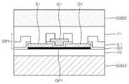
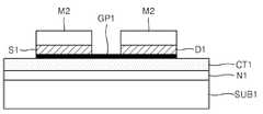
도 3a를 참조하면, 도 1a 내지 도 1g의 방법과 유사한 방법을 사용해서, 제1 기판(SUB1) 상에 소자부(DP1')가 마련되고, 소자부(DP1') 상에 제2 기판(SUB2)이 부착된 구조물을 마련할 수 있다. 이때, 소자부(DP1')는 그래핀층(GP1), 소오스전극(S1), 드레인전극(D1), 게이트절연층(GI1) 및 게이트(G1)를 포함할 수 있고, 이들을 덮는 절연층(IL1)을 더 포함할 수 있다. 도 3a의 구조에서는 도 1g의 구조와 달리 절연층(IL1) 및 게이트절연층(GI1)이 패터닝(식각)되지 않을 수 있다. 절연층(IL1) 상에 제1 보호층(P1)이 구비될 수 있고, 제1 보호층(P1) 상에 제2 기판(SUB2)이 부착될 수 있다.Referring to FIG. 3A, by using a method similar to the method of FIGS. 1A to 1G, an element portion DP1 ′ is provided on the first substrate SUB1 and a second substrate (on the element portion DP1 ′). A structure to which SUB2) is attached can be provided. In this case, the device portion DP1 ′ may include a graphene layer GP1, a source electrode S1, a drain electrode D1, a gate insulating layer GI1, and a gate G1, and may cover the insulating layer IL1. ) May be further included. In the structure of FIG. 3A, unlike the structure of FIG. 1G, the insulating layer IL1 and the gate insulating layer GI1 may not be patterned (etched). The first passivation layer P1 may be provided on the insulating layer IL1, and the second substrate SUB2 may be attached to the first passivation layer P1.
도 3b를 참조하면, 도 1h의 단계와 유사하게, 제1 기판(SUB1)을 제거/분리할 수 있다. 본 실시예에서는 촉매층(CT1)을 식각하여 제1 기판(SUB1)을 제거/분리하는 경우가 도시되어 있지만, 중간층(N1)을 식각하여 제1 기판(SUB1)을 제거/분리할 수도 있다. 중간층(N1)을 식각하여 제1 기판(SUB1)을 제거/분리하는 경우, 촉매층(CT1)을 제거하는 공정을 별도로 수행할 수 있다.Referring to FIG. 3B, similar to the step of FIG. 1H, the first substrate SUB1 may be removed / separated. In the present exemplary embodiment, a case in which the first substrate SUB1 is removed / separated by etching the catalyst layer CT1 may be removed, but the first substrate SUB1 may be removed / separated by etching the intermediate layer N1. When the first substrate SUB1 is removed / separated by etching the intermediate layer N1, a process of removing the catalyst layer CT1 may be separately performed.
도 3c를 참조하면, 소자부(DP1')가 형성된 제2 기판(SUB2)을 위·아래로 뒤집은 상태에서 소자부(DP1') 상에 제2 절연층(IL2)을 형성할 수 있다. 제2 절연층(IL2)은 절연층(IL1)(이하, 제1 절연층)과 동일하거나 유사한 물질로 형성할 수 있다. 제2 절연층(IL2)은 그래핀층(GP1)에 손상을 주지 않는 방법, 예컨대, 예컨대, 열(thermal) ALD, 열(thermal) CVD, 증발(evaporation) 법 등으로 형성할 수 있다.Referring to FIG. 3C, the second insulating layer IL2 may be formed on the element portion DP1 ′ with the second substrate SUB2 on which the element portion DP1 ′ is formed upside down. The second insulating layer IL2 may be formed of the same or similar material as the insulating layer IL1 (hereinafter, referred to as a first insulating layer). The second insulating layer IL2 may be formed by a method that does not damage the graphene layer GP1, for example, thermal ALD, thermal CVD, evaporation, or the like.
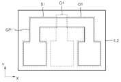
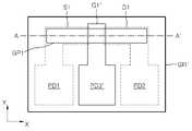
도 3c의 소자부(DP1')는, 예컨대, 도 4a에 도시된 바와 같은 평면 구조를 가질 수 있다. 도 4a를 참조하면, 그래핀층(GP1)은 X축 방향으로 연장된 형상을 가질 수 있다. 소오스전극(S1)은 그래핀층(GP1)의 일단에 접촉하면서, 그래핀층(GP1)의 외측으로 연장된 제1 패드부(PD1)를 포함할 수 있다. 이와 유사하게, 드레인전극(D1)은 그래핀층(GP1)의 타단에 접촉하면서, 그래핀층(GP1)의 외측으로 연장된 제2 패드부(PD2)를 포함할 수 있다. 게이트(G1)는 그래핀층(GP1)의 중앙부에 오버랩되면서 Y축 방향으로 연장된 제3 패드부(PD3)를 포함할 수 있다. 제2 절연층(IL2)은 그래핀층(GP1), 소오스전극(S1), 드레인전극(D1) 및 게이트(G1)를 덮도록 구비될 수 있다. 도 4a의 A-A'선에 따른 단면도가 도 3c와 같을 수 있다. 따라서, 도 3c에는 도시되지 않았지만, 소오스전극(S1), 드레인전극(D1) 및 게이트(G1)는 각각 제1 패드부(PD1), 제2 패드부(PD2) 및 제3 패드부(PD3)를 포함할 수 있다.The element portion DP1 ′ of FIG. 3C may have, for example, a planar structure as shown in FIG. 4A. Referring to FIG. 4A, the graphene layer GP1 may have a shape extending in the X-axis direction. The source electrode S1 may include a first pad portion PD1 extending to the outside of the graphene layer GP1 while being in contact with one end of the graphene layer GP1. Similarly, the drain electrode D1 may include a second pad portion PD2 extending to the outside of the graphene layer GP1 while being in contact with the other end of the graphene layer GP1. The gate G1 may include a third pad portion PD3 extending in the Y-axis direction while overlapping the center portion of the graphene layer GP1. The second insulating layer IL2 may be provided to cover the graphene layer GP1, the source electrode S1, the drain electrode D1, and the gate G1. A cross-sectional view taken along line AA ′ of FIG. 4A may be the same as that of FIG. 3C. Therefore, although not shown in FIG. 3C, the source electrode S1, the drain electrode D1, and the gate G1 are respectively the first pad part PD1, the second pad part PD2, and the third pad part PD3. It may include.
다음, 도 3d와 같은 구조를 형성할 수 있다. 도 3d는 도 4a의 제1 내지 제3 패드부(PD1∼PD3)에 대한 공정일 수 있다. 보다 구체적으로 설명하면, 제2 절연층(IL2)의 일부 및 게이트절연층(GI1)의 일부를 식각하여 제1 내지 제3 패드부(PD1∼PD3)를 노출시키는 제1 내지 제3 콘택홀(H1∼H3)을 형성할 수 있다. 도 3d의 단면 구조는 도 4b의 평면 구조에 대응될 수 있다. 도 4b의 B-B'선에 따른 단면도가 도 3d와 같을 수 있다.Next, a structure as shown in FIG. 3D may be formed. 3D may be a process for the first to third pad parts PD1 to PD3 of FIG. 4A. More specifically, the first to third contact holes exposing the first to third pad parts PD1 to PD3 by etching part of the second insulating layer IL2 and a part of the gate insulating layer GI1 may be exposed. H1 to H3) can be formed. The cross-sectional structure of FIG. 3D may correspond to the planar structure of FIG. 4B. A cross-sectional view taken along the line BB ′ of FIG. 4B may be the same as that of FIG. 3D.
도 4a 및 도 4b에서 그래핀층(GP1), 소오스전극(S1), 드레인전극(D1) 및 게이트(G1)의 형상은 예시적인 것이고, 이들의 형상은 다양하게 변형될 수 있다. 예컨대, 그래핀층(GP1)은 도 5에 도시된 바와 같은 구조로 변형될 수 있다. 도 5를 참조하면, 그래핀층(GP1')은 소오스전극(S1) 및 드레인전극(D1)과 동일하거나 거의 유사한 평면 구조를 가지면서, 소오스전극(S1) 및 드레인전극(D1) 사이의 중앙부가 연결된 구조를 가질 수 있다. 즉, 그래핀층(GP1)은 소오스전극(S1)과 동일하거나 거의 유사한 평면 구조를 갖는 제1 영역, 드레인전극(D1)과 동일하거나 거의 유사한 평면 구조를 갖는 제2 영역, 및 상기 제1 영역과 제2 영역을 연결하는 제3 영역(중앙부)을 포함할 수 있다. 도 2a 내지 도 2d를 참조하여 설명한 바와 같이, 제1 마스크패턴(도 2b의 M1)으로 그래핀층(GP1)과 소오스/드레인용 도전층(SD1)을 순차로 패터닝하면, 이들은 동일한 평면 구조를 가질 수 있고, 후속 공정으로 제2 마스크패턴(도 2c의 M2)을 이용해서 소오스/드레인용 도전층(SD1)을 2차로 패터닝하면 소오스전극(S1) 및 드레인전극(D1)을 형성하면서 이들 사이의 채널영역(상기 제3 영역)을 노출시킬 수 있다.4A and 4B, the shapes of the graphene layer GP1, the source electrode S1, the drain electrode D1, and the gate G1 are exemplary, and their shapes may be variously modified. For example, the graphene layer GP1 may be modified to have a structure as shown in FIG. 5. Referring to FIG. 5, the graphene layer GP1 ′ has the same or substantially similar planar structure as the source electrode S1 and the drain electrode D1, and has a central portion between the source electrode S1 and the drain electrode D1. It may have a connected structure. That is, the graphene layer GP1 may have a first region having the same or substantially similar planar structure as the source electrode S1, a second region having the same or substantially similar planar structure as the drain electrode D1, and the first region. It may include a third region (center portion) connecting the second region. As described with reference to FIGS. 2A to 2D, when the graphene layer GP1 and the source / drain conductive layer SD1 are sequentially patterned with the first mask pattern M1 of FIG. 2B, they may have the same planar structure. In the subsequent process, the source / drain conductive layer SD1 is secondarily patterned using the second mask pattern (M2 in FIG. 2C) to form the source electrode S1 and the drain electrode D1, The channel region (the third region) may be exposed.
도 3a 내지 도 3d를 참조하여 설명한 실시예에서는 제2 기판(SUB2)이 최종 소자의 기판으로 사용되고, 도 1j의 제3 기판(SUB3)의 부착 공정 및 도 1k의 제2 기판(SUB2)의 제거 공정 등이 생략될 수 있다. 이렇게 공정수가 감소함에 따라, 전체적인 제조공정이 단순화될 수 있다. 또한, 도 3a 내지 도 3d의 방법에서는 소자부(DP1')의 양측(즉, 하측 및 상측)에 제1 기판(SUB1) 및 제2 기판(SUB2)이 마련된 상태에서 제1 기판(SUB1)을 제거하고 제2 기판(SUB2)을 최종 기판으로 사용하므로, 그래핀층(GP1)의 직접적인 전이(transfer) 공정은 포함되지 않는다고 할 수 있다. 따라서 본 실시예의 방법은 그래핀의 전이 없이 그래핀 소자를 제조하는 공정(즉, transfer-free process)이라고 할 수 있다.In the embodiment described with reference to FIGS. 3A to 3D, the second substrate SUB2 is used as the substrate of the final device, and the attachment process of the third substrate SUB3 of FIG. 1J and the removal of the second substrate SUB2 of FIG. 1K are performed. The process and the like can be omitted. As the number of processes is reduced in this way, the overall manufacturing process can be simplified. In addition, in the method of FIGS. 3A to 3D, the first substrate SUB1 is disposed in a state where the first substrate SUB1 and the second substrate SUB2 are provided on both sides (ie, the lower side and the upper side) of the element portion DP1 ′. Since the second substrate SUB2 is removed and used as the final substrate, the direct transfer process of the graphene layer GP1 may not be included. Therefore, the method of the present embodiment may be referred to as a process (ie, a transfer-free process) of manufacturing a graphene device without the transfer of graphene.
도 4b의 A-A'선에 따른 단면도는 도 3c와 같을 수 있으므로, 도 3c의 구조는 본 발명의 실시예에 따른 트랜지스터의 단면도라고 할 수 있다.Since the cross-sectional view taken along the line A-A 'of FIG. 4B may be the same as that of FIG. 3C, the structure of FIG. 3C may be referred to as a cross-sectional view of the transistor according to the embodiment of the present invention.
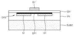
도 3c를 참조하여 본 발명의 실시예에 따른 트랜지스터를 설명하면 다음과 같다. 제2 기판(SUB2) 상에 제1 보호층(P1)이 구비될 수 있고, 제1 보호층(P1) 상에 제1 절연층(IL1)이 구비될 수 있다. 제2 기판(SUB2)은, 예컨대, 폴리머 기판일 수 있다. 제1 보호층(P1)은 절연 물질로 형성될 수 있으므로, 제1 보호층(P1)과 제1 절연층(IL1)이 다층 구조의 절연층을 구성한다고 할 수 있다. 제1 절연층(IL1)은 표면부에 오목한 영역을 가질 수 있고, 상기 오목한 영역에 '그래핀 소자부'가 구비될 수 있다. 상기 그래핀 소자부는 게이트(G1), 게이트(G1) 상에 구비된 게이트절연층(GI1), 게이트(G1) 양측의 게이트절연층(GI1) 상에 구비된 소오스전극(S1) 및 드레인전극(D1), 그리고 소오스전극(S1) 및 드레인전극(D1)에 접촉하도록 구비된 그래핀층(GP1)을 포함할 수 있다. 그래핀층(GP1)은 채널층일 수 있다. 게이트절연층(GI1)은 그래핀층(GP1) 양측의 제1 절연층(IL1) 위로 연장된 구조를 가질 수 있다. 제1 절연층(IL1) 위로 연장된 게이트절연층(GI1) 부분은 그래핀층(GP1)과 동일한(혹은 유사한) 높이에 구비될 수 있다. 게이트(G1)는 소오스전극(S1) 및 드레인전극(D1)과 오버랩(overlap)된 구조를 가질 수 있다. 그래핀층(GP1) 및 게이트절연층(GI1)을 덮는 제2 절연층(IL2)이 구비될 수 있다.A transistor according to an embodiment of the present invention will be described with reference to FIG. 3C. The first passivation layer P1 may be provided on the second substrate SUB2, and the first insulation layer IL1 may be provided on the first passivation layer P1. The second substrate SUB2 may be, for example, a polymer substrate. Since the first protective layer P1 may be formed of an insulating material, it may be said that the first protective layer P1 and the first insulating layer IL1 form an insulating layer having a multilayer structure. The first insulating layer IL1 may have a concave region on the surface portion, and the graphene element portion may be provided in the concave region. The graphene device unit may include a gate electrode S1 and a drain electrode provided on the gate G1, the gate insulating layer GI1 provided on the gate G1, and the gate insulating layer GI1 on both sides of the gate G1. D1) and the graphene layer GP1 provided to contact the source electrode S1 and the drain electrode D1. The graphene layer GP1 may be a channel layer. The gate insulating layer GI1 may have a structure extending over the first insulating layer IL1 on both sides of the graphene layer GP1. A portion of the gate insulating layer GI1 extending over the first insulating layer IL1 may be provided at the same height as (or similar to) the graphene layer GP1. The gate G1 may have a structure overlapping with the source electrode S1 and the drain electrode D1. A second insulating layer IL2 covering the graphene layer GP1 and the gate insulating layer GI1 may be provided.
도 6a 내지 도 6d는 본 발명의 다른 실시예에 따른 그래핀 소자의 제조방법을 보여주는 단면도이다.6A through 6D are cross-sectional views illustrating a method of manufacturing a graphene device according to another exemplary embodiment of the present invention.
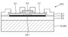
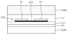
도 6a를 참조하면, 도 1b의 구조물이 마련된 상태에서, 제1 기판(SUB1) 상에 소오스전극(S1), 드레인전극(D1) 및 그래핀층(GP1)을 덮는 보호층(P1)을 형성할 수 있다. 보호층(P1)은 도 1f의 제1 보호층(P1)과 동일한(혹은 유사한) 물질 및 방법으로 형성할 수 있다. 다음, 보호층(P1) 상에 제2 기판(SUB2)을 부착할 수 있다. 제2 기판(SUB2)은 도 1g의 제2 기판(SUB2)과 동일한(혹은 유사한) 물질 및 방법으로 형성할 수 있다. 경우에 따라서는, 보호층(P1)과 제2 기판(SUB2) 사이에 소정의 접착층(미도시)을 더 구비시킬 수도 있다. 그래핀층(GP1), 소오스전극(S1) 및 드레인전극(D1)은 하나의 소자부(DP2)를 구성한다고 할 수 있다. 여기서, 소자부(DP2)는 도 1e의 소자부(DP1)와 달리 미완성 상태의 소자부일 수 있다.Referring to FIG. 6A, when the structure of FIG. 1B is provided, a passivation layer P1 covering the source electrode S1, the drain electrode D1, and the graphene layer GP1 may be formed on the first substrate SUB1. Can be. The protective layer P1 may be formed of the same (or similar) material and method as the first protective layer P1 of FIG. 1F. Next, the second substrate SUB2 may be attached onto the protective layer P1. The second substrate SUB2 may be formed of the same (or similar) material and method as the second substrate SUB2 of FIG. 1G. In some cases, a predetermined adhesive layer (not shown) may be further provided between the protective layer P1 and the second substrate SUB2. The graphene layer GP1, the source electrode S1, and the drain electrode D1 may constitute one element portion DP2. Here, the device portion DP2 may be an unfinished device portion unlike the device portion DP1 of FIG. 1E.
도 6b를 참조하면, 제1 기판(SUB1)을 제거/분리할 수 있다. 제1 기판(SUB1)은 촉매층(CT1)이나 중간층(N1)을 식각함으로써 제거/분리될 수 있다. 본 실시예에서는 촉매층(CT1)을 식각하여 제1 기판(SUB1)을 제거/분리하는 경우가 도시되어 있다. 제1 기판(SUB1)의 제거/분리 방법은 도 1h를 참조하여 설명한 바와 동일하거나 유사할 수 있고, 다양하게 변형될 수 있다.Referring to FIG. 6B, the first substrate SUB1 may be removed / separated. The first substrate SUB1 may be removed / separated by etching the catalyst layer CT1 or the intermediate layer N1. In this embodiment, a case where the first substrate SUB1 is removed / separated by etching the catalyst layer CT1 is illustrated. The removal / separation method of the first substrate SUB1 may be the same as or similar to that described with reference to FIG. 1H, and may be variously modified.
도 6c를 참조하면, 그래핀층(GP1), 소오스전극(S1) 및 드레인전극(D1) 등이 형성된 제2 기판(SUB2)을 위·아래로 뒤집은 상태에서, 그래핀층(GP1) 및 보호층(P10) 상에 게이트절연층(GI1')을 형성할 수 있다. 게이트절연층(GI1')은 도 1c의 게이트절연층(GI1)과 동일한(혹은 유사한) 물질 및 방법으로 형성할 수 있다. 게이트절연층(GI1') 상에 게이트(G1')를 형성할 수 있다. 게이트(G1')는 소오스전극(S1)과 드레인전극(D1) 사이의 그래핀층(GP1) 위쪽에 구비될 수 있다.Referring to FIG. 6C, in the state in which the second substrate SUB2 including the graphene layer GP1, the source electrode S1, the drain electrode D1, and the like is turned upside down, the graphene layer GP1 and the protective layer ( A gate insulating layer GI1 ′ may be formed on P10. The gate insulating layer GI1 ′ may be formed of the same (or similar) material and method as the gate insulating layer GI1 of FIG. 1C. The gate G1 'may be formed on the gate insulating layer GI1'. The gate G1 ′ may be provided above the graphene layer GP1 between the source electrode S1 and the drain electrode D1.
도 6c의 트랜지스터는 도 7a에 도시된 바와 같은 평면 구조를 가질 수 있다. 도 7a의 평면 구조는 도 4a의 평면 구조와 유사하다. 단, 도 7a에서 게이트(G1')는 그래핀층(GP1) 및 게이트절연층(GI1') 위에 구비된다. 도 7a의 참조번호 PD1, PD2, PD3'는 각각 제1 패드부, 제2 패드부 및 제3 패드부를 나타낸다. 도 7a의 A-A'선에 따른 단면도가 도 6c와 같을 수 있다.The transistor of FIG. 6C may have a planar structure as shown in FIG. 7A. The planar structure of FIG. 7A is similar to the planar structure of FIG. 4A. In FIG. 7A, the gate G1 ′ is provided on the graphene layer GP1 and the gate insulating layer GI1 ′. Reference numerals PD1, PD2, and PD3 'of FIG. 7A denote first pad portions, second pad portions, and third pad portions, respectively. A cross-sectional view taken along line AA ′ of FIG. 7A may be the same as that of FIG. 6C.
다음, 도 6d와 같은 구조를 형성할 수 있다. 도 6d는 도 7a의 제1 및 제2 패드부(PD1, PD2)에 대한 공정일 수 있다. 보다 구체적으로 설명하면, 게이트절연층(GI1')의 일부를 식각하여 제1 및 제2 패드부(PD1, PD2)를 노출시키는 제1 및 제2 콘택홀(H1', H2')을 형성할 수 있다. 도 6d의 단면 구조는 도 7b의 평면 구조에 대응될 수 있다. 도 7b의 B-B'선에 따른 단면도가 도 6d와 같을 수 있다. 도 7a 및 도 7b에서 그래핀층(GP1), 소오스전극(S1), 드레인전극(D1) 및 게이트(G1')의 형상은 예시적인 것이고, 이들의 형상은 다양하게 변형될 수 있다. 예컨대, 그래핀층(GP1)은 도 5의 그래핀층(GP1')과 동일하거나 유사한 형상을 가질 수 있다.Next, a structure as shown in FIG. 6D may be formed. FIG. 6D may be a process for the first and second pad parts PD1 and PD2 of FIG. 7A. In more detail, a portion of the gate insulating layer GI1 ′ may be etched to form first and second contact holes H1 ′ and H2 ′ exposing the first and second pad portions PD1 and PD2. Can be. The cross-sectional structure of FIG. 6D may correspond to the planar structure of FIG. 7B. A cross-sectional view taken along the line BB ′ of FIG. 7B may be the same as that of FIG. 6D. 7A and 7B, the shapes of the graphene layer GP1, the source electrode S1, the drain electrode D1, and the gate G1 ′ are exemplary, and their shapes may be variously modified. For example, the graphene layer GP1 may have the same or similar shape as the graphene layer GP1 ′ of FIG. 5.
도 6a 내지 도 6d를 참조하여 설명한 실시예에서는 제2 기판(SUB2)이 최종 기판으로 사용되고, 도 1j의 제3 기판(SUB3)의 부착 공정 및 도 1k의 제2 기판(SUB2)의 제거 공정 등이 생략될 수 있다. 따라서 공정이 단순화될 수 있다. 또한, 도 6a 내지 도 6d의 방법에서는 소자부(DP2)의 양측(즉, 하측 및 상측)에 제1 기판(SUB1) 및 제2 기판(SUB2)이 마련된 상태에서 제1 기판(SUB1)을 제거하고 제2 기판(SUB2)을 최종 기판으로 사용하므로, 그래핀층(GP1)의 직접적인 전이(transfer) 공정은 포함되지 않는다고 할 수 있다. 그러므로, 그래핀층의 직접적인 전이에 따른 그래핀층의 손상 및 오염 문제를 방지 또는 최소화할 수 있다.In the exemplary embodiment described with reference to FIGS. 6A to 6D, the second substrate SUB2 is used as the final substrate, the attaching process of the third substrate SUB3 of FIG. 1J, the removing process of the second substrate SUB2 of FIG. 1K, and the like. This can be omitted. Thus, the process can be simplified. In addition, in the method of FIGS. 6A to 6D, the first substrate SUB1 is removed while the first substrate SUB1 and the second substrate SUB2 are provided on both sides (ie, the lower side and the upper side) of the element portion DP2. In addition, since the second substrate SUB2 is used as the final substrate, the direct transfer process of the graphene layer GP1 may not be included. Therefore, it is possible to prevent or minimize the problem of damage and contamination of the graphene layer due to the direct transition of the graphene layer.
도 7b의 A-A'선에 따른 단면도는 도 6c와 같을 수 있으므로, 도 6c의 구조는 본 발명의 실시예에 따른 트랜지스터의 단면도라고 할 수 있다.Since the cross-sectional view taken along line AA ′ of FIG. 7B may be the same as that of FIG. 6C, the structure of FIG. 6C may be referred to as a cross-sectional view of a transistor according to an exemplary embodiment of the present invention.
도 6c를 참조하여 본 발명의 실시예에 따른 트랜지스터를 설명하면 다음과 같다. 제2 기판(SUB2) 상에 보호층(P1)이 구비될 수 있다. 제2 기판(SUB2)은, 예컨대, 폴리머 기판일 수 있다. 보호층(P1) 내에 서로 이격된 소오스전극(S1) 및 드레인전극(D1)이 구비될 수 있다. 소오스전극(S1)과 드레인전극(D1)을 연결하는 그래핀층(GP1)이 구비될 수 있다. 소오스전극(S1) 및 드레인전극(D1)은 그래핀층(GP1)의 제1 영역 및 제2 영역 아래에 구비될 수 있다. 그래핀층(GP1)은 보호층(P1)의 상면과 동일한 높이로 구비될 수 있다. 다시 말해, 그래핀층(GP1)의 상면과 그 주위의 보호층(P1)의 상면은 동일한 레벨(높이)을 가질 수 있다. 보호층(P1) 상에 그래핀층(GP1)을 덮는 게이트절연층(GI1')이 구비될 수 있다. 게이트절연층(GI1') 상에 게이트(G1')가 구비될 수 있다. 게이트(G1')는 소오스전극(S1) 및 드레인전극(D1) 사이의 그래핀층(GP1) 위쪽에 구비될 수 있다.A transistor according to an embodiment of the present invention will be described with reference to FIG. 6C. The protective layer P1 may be provided on the second substrate SUB2. The second substrate SUB2 may be, for example, a polymer substrate. The source electrode S1 and the drain electrode D1 spaced apart from each other may be provided in the passivation layer P1. A graphene layer GP1 connecting the source electrode S1 and the drain electrode D1 may be provided. The source electrode S1 and the drain electrode D1 may be provided under the first and second regions of the graphene layer GP1. The graphene layer GP1 may be provided at the same height as the upper surface of the protective layer P1. In other words, the upper surface of the graphene layer GP1 and the upper surface of the protective layer P1 around the graphene layer GP1 may have the same level (height). A gate insulating layer GI1 ′ covering the graphene layer GP1 may be provided on the passivation layer P1. The gate G1 'may be provided on the gate insulating layer GI1'. The gate G1 ′ may be provided above the graphene layer GP1 between the source electrode S1 and the drain electrode D1.
본 발명의 다른 실시예에 따르면, 제1 기판(SUB1) 상에 복수의 소자부(DP1)를 형성할 수 있고, 패터닝 공정을 통해 복수의 소자부(DP1)를 분리한 뒤, 제1 기판(SUB1)의 제거 공정을 수행할 수 있다. 이에 대해서는 도 8a 내지 도 8e를 참조하여 보다 상세하게 설명한다.According to another embodiment of the present invention, the plurality of device portions DP1 may be formed on the first substrate SUB1, and after separating the plurality of device portions DP1 through a patterning process, the first substrate ( The removal process of SUB1) can be performed. This will be described in more detail with reference to FIGS. 8A to 8E.
도 8a를 참조하면, 제1 기판(SUB10) 상에 복수의 소자부(DP10)를 포함하는 적층 구조물(소자층)을 형성할 수 있다. 각각의 소자부(DP10)는 도 1f의 소자부(DP1)와 동일한 구조를 가질 수 있다. 본 단계에서 복수의 소자부(DP10)를 포함하는 상기 적층 구조물(소자층)은 연속적인 구조를 가질 수 있다. 제1 기판(SUB10)과 복수의 소자부(DP10) 사이에는 촉매층(CT10)이 구비될 수 있다. 제1 기판(SUB10)과 촉매층(CT10) 사이에는 중간층(N10)이 더 구비될 수 있다. 참조번호 GP10, S10, D10, GI10, G10, IL10, P10은 각각 그래핀층, 소오스전극, 드레인전극, 게이트절연층, 게이트, 절연층, 보호층을 나타낸다.Referring to FIG. 8A, a stacked structure (element layer) including a plurality of element portions DP10 may be formed on the first substrate SUB10. Each device portion DP10 may have the same structure as the device portion DP1 of FIG. 1F. In this step, the stack structure (element layer) including the plurality of element portions DP10 may have a continuous structure. The catalyst layer CT10 may be provided between the first substrate SUB10 and the plurality of device units DP10. An intermediate layer N10 may be further provided between the first substrate SUB10 and the catalyst layer CT10. Reference numerals GP10, S10, D10, GI10, G10, IL10, and P10 denote graphene layers, source electrodes, drain electrodes, gate insulating layers, gates, insulating layers and protective layers, respectively.
도 8b를 참조하면, 제1 기판(SUB10) 상에 형성된 적층 구조물, 즉, 복수의 소자부(DP10)를 포함하는 소자층을 패터닝하여 복수의 소자부(DP10)를 분리시킬 수 있다. 상기 패터닝 공정은 보호층(P10)에서 중간층(N10)까지 식각하여 제1 기판(SUB10)의 상면이 노출될 때까지 수행할 수 있다. 상기 식각 공정은 보호층(P10)에서 촉매층(CT10)까지만 수행할 수도 있다. 이 경우, 중간층(N10)은 식각되지 않고 연속된 층 형상을 유지할 수 있다. 상기 패터닝 공정에 의해 소자부(DP10)들 사이에 일종의 트렌치(trench)(T10)가 형성될 수 있다. 상기 패터닝 공정에 의해 분리된 복수의 소자부(DP10)들은 위에서 보았을 때, 복수의 행과 열을 이루도록 규칙적으로 배열될 수 있다. 복수의 소자부(DP10) 사이에 형성된 트렌치(T10)는 위에서 보았을 때, 그물망(mesh) 구조와 유사한 구조를 가질 수 있다. 이런 점에서, 상기 패터닝 공정은 메쉬(mesh) 패터닝이라 할 수 있다.Referring to FIG. 8B, a plurality of device units DP10 may be separated by patterning a stacked structure formed on the first substrate SUB10, that is, a device layer including a plurality of device units DP10. The patterning process may be performed from the protective layer P10 to the intermediate layer N10 until the top surface of the first substrate SUB10 is exposed. The etching process may be performed only from the protective layer P10 to the catalyst layer CT10. In this case, the intermediate layer N10 may maintain a continuous layer shape without being etched. A type of trench T10 may be formed between the device portions DP10 by the patterning process. The plurality of device units DP10 separated by the patterning process may be regularly arranged to form a plurality of rows and columns when viewed from above. The trench T10 formed between the plurality of device units DP10 may have a structure similar to a mesh structure when viewed from above. In this regard, the patterning process may be referred to as mesh patterning.
도 8c를 참조하면, 복수의 소자부(DP10) 상에 제2 기판(SUB20)을 부착할 수 있다. 복수의 소자부(DP10) 사이에 트렌치(T10)가 형성되어 있으므로, 제2 기판(SUB20)의 부착시 트렌치(T10)로 기포(공기)가 빠져나갈 수 있다. 따라서, 제2 기판(SUB2)의 부착은 용이하게 이루어질 수 있다. 제2 기판(SUB20)은 복수의 소자부(DP10)를 지지하는 역할을 할 수 있다. 제2 기판(SUB20)은 도 1g의 제2 기판(SUB2)과 동일하거나 유사한 물질로 구성된 기판일 수 있다.Referring to FIG. 8C, the second substrate SUB20 may be attached onto the plurality of device units DP10. Since the trenches T10 are formed between the plurality of device units DP10, bubbles (air) may escape to the trenches T10 when the second substrate SUB20 is attached. Therefore, attachment of the second substrate SUB2 may be easily performed. The second substrate SUB20 may serve to support the plurality of device units DP10. The second substrate SUB20 may be a substrate made of the same or similar material as the second substrate SUB2 of FIG. 1G.
도 8d를 참조하면, 복수의 소자부(DP10) 사이의 트렌치(T10)를 통해 소정의 식각액(미도시)을 주입하여 촉매층(CT10) 또는 중간층(N10)에 대한 식각 공정을 수행할 수 있다. 본 실시예에서는 촉매층(CT10)에 대한 식각 공정을 수행한 경우가 도시되어 있다. 복수의 소자부(DP10) 사이로 식각액이 용이하게 주입될 수 있으므로, 촉매층(CT10)의 식각은 용이하게 이루어질 수 있다. 제1 기판(SUB10)이 대면적의 기판이라고 하더라도, 촉매층(CT10)을 용이하게 그리고 단시간에 제거할 수 있다. 이는 곧, 제1 기판(SUB10)을 용이하게 제거/분리할 수 있다는 것을 의미한다. 여기서, 촉매층(CT10)은 제1 기판(SUB10)을 제거하기 위해 식각되는 층이므로, 일종의 희생층이라 할 수 있다. 만약, 촉매층(CT10)이 아닌 중간층(N10)을 식각하여 제1 기판(SUB10)을 제거하는 경우에는, 중간층(N10)을 희생층이라 할 수 있다. 촉매층(CT10)은 금속층일 수 있고, 중간층(N10)은 절연층일 수 있으므로, 상기 희생층은 금속층 또는 절연층일 수 있다.Referring to FIG. 8D, an etching solution (not shown) may be injected through the trenches T10 between the plurality of device units DP10 to perform an etching process on the catalyst layer CT10 or the intermediate layer N10. In this embodiment, the etching process for the catalyst layer CT10 is shown. Since the etchant may be easily injected between the plurality of device units DP10, the catalyst layer CT10 may be easily etched. Even if the first substrate SUB10 is a large-area substrate, the catalyst layer CT10 can be removed easily and in a short time. This means that the first substrate SUB10 can be easily removed / separated. Here, the catalyst layer CT10 is a layer that is etched to remove the first substrate SUB10, and thus may be called a sacrificial layer. If the first substrate SUB10 is removed by etching the intermediate layer N10 instead of the catalyst layer CT10, the intermediate layer N10 may be referred to as a sacrificial layer. Since the catalyst layer CT10 may be a metal layer and the intermediate layer N10 may be an insulating layer, the sacrificial layer may be a metal layer or an insulating layer.
도 8d에서 제1 기판(SUB10)이 제거/분리된 결과물은 도 8e에 도시된 바와 같을 수 있다. 도 8e에서 각각의 소자부(DP10)는 도 1h의 소자부(DP1)와 동일한 구조를 갖는다고 할 수 있다. 이후, 도시하지는 않았지만, 도 8e의 구조에 대해서 소정의 후속 공정을 수행할 수 있다. 상기 후속 공정은 도 1i 내지 도 1l의 공정과 유사할 수 있다. 도 8a 내지 도 8e의 방법은 도 1a 내지 도 1l의 공정뿐 아니라, 도 3a 내지 도 3d의 공정 및 도 6a 내지 도 6d의 공정에도 유사하게 적용될 수 있다.In FIG. 8D, the result of removing / separating the first substrate SUB10 may be as shown in FIG. 8E. In FIG. 8E, each element portion DP10 may have the same structure as that of the element portion DP1 of FIG. 1H. Thereafter, although not shown, certain subsequent processes may be performed on the structure of FIG. 8E. The subsequent process may be similar to the process of FIGS. 1I-1L. 8A-8E can be similarly applied to the processes of FIGS. 3A-3D and the processes of FIGS. 6A-6D, as well as the processes of FIGS. 1A-1L.
도 8a 내지 도 8e의 방법을 사용하면, 300㎜ 이상의 지름을 갖는 대면적 기판에 대해서도 본원의 실시예에 따른 그래핀 소자의 제조방법을 용이하게 적용할 수 있다. 따라서 본 실시예의 방법을 사용하면, 그래핀 소자의 생산성을 향상시킬 수 있고, 제조 단가를 낮출 수 있다.Using the method of FIGS. 8A to 8E, the method for manufacturing a graphene device according to the embodiment of the present application can be easily applied to a large area substrate having a diameter of 300 mm or more. Therefore, by using the method of this embodiment, the productivity of the graphene device can be improved, and the manufacturing cost can be reduced.
상기한 설명에서 많은 사항이 구체적으로 기재되어 있으나, 그들은 발명의 범위를 한정하는 것이라기보다, 바람직한 실시예의 예시로서 해석되어야 한다. 예들 들어, 본 발명이 속하는 기술 분야에서 통상의 지식을 가진 자라면, 전술한 본 발명의 실시예에 따른 그래핀 소자의 제조방법 및 이 방법으로 형성된 그래핀 소자는 다양하게 변형될 수 있음을 알 수 있을 것이다. 또한 본 발명의 실시예는 그래핀 트랜지스터가 아닌 그 밖의 그래핀 소자에도 적용될 수 있음을 알 수 있을 것이다. 때문에 본 발명의 범위는 설명된 실시예에 의하여 정하여 질 것이 아니고 특허 청구범위에 기재된 기술적 사상에 의해 정하여져야 한다.Although a number of matters have been specifically described in the above description, they should be interpreted as examples of preferred embodiments rather than limiting the scope of the invention. For example, those skilled in the art to which the present invention pertains, the graphene device manufacturing method and the graphene device formed by the method according to the embodiment of the present invention described above may be variously modified. Could be. In addition, it will be appreciated that embodiments of the present invention may be applied to other graphene devices other than graphene transistors. Therefore, the scope of the present invention is not to be determined by the described embodiments but should be determined by the technical idea described in the claims.
CT1, CT10 : 촉매층 D1, D10 : 드레인전극
DP1, DP2, DP10 : 소자부 G1, G10 : 게이트
GI1, GI10 : 게이트절연층 GP1, GP10 : 그래핀층
H1, H2, H3 : 콘택홀 IL1, IL2, IL10 : 절연층
M1, M2 : 마스크패턴 N1, N10 : 중간층
P1, P2, P10 : 보호층 PD1, PD2, PD3 : 패드부
S1, S10 : 소오스전극 SD1 : 소오스/드레인용 도전층
SUB1, SUB10 : 제1 기판 SUB2, SUB20 : 제2 기판
SUB3 : 제3 기판 T10 : 트렌치CT1, CT10: catalyst layer D1, D10: drain electrode
DP1, DP2, DP10: element section G1, G10: gate
GI1, GI10: Gate Insulation Layer GP1, GP10: Graphene Layer
H1, H2, H3: contact hole IL1, IL2, IL10: insulating layer
M1, M2: mask pattern N1, N10: intermediate layer
P1, P2, P10: protective layer PD1, PD2, PD3: pad part
S1, S10: source electrode SD1: source / drain conductive layer
SUB1, SUB10: first substrate SUB2, SUB20: second substrate
SUB3: third substrate T10: trench
Claims (32)
Translated fromKorean상기 제1 기판 상에 상기 그래핀층을 포함하는 소자부를 형성하는 단계;
상기 제1 기판의 상기 소자부 측에 제2 기판을 부착하는 단계; 및
상기 제1 기판을 제거하는 단계;를 포함하는 그래핀 소자의 제조방법.Forming a graphene layer on the first substrate;
Forming an element part including the graphene layer on the first substrate;
Attaching a second substrate to the element portion side of the first substrate; And
Removing the first substrate; Method of manufacturing a graphene device comprising a.
상기 그래핀층의 제1 영역 및 제2 영역에 각각 접촉된 소오스전극 및 드레인전극을 형성하는 단계;를 포함하는 그래핀 소자의 제조방법.The method of claim 1, wherein the forming of the device portion,
Forming a source electrode and a drain electrode in contact with the first and second regions of the graphene layer, respectively.
상기 그래핀층, 소오스전극 및 드레인전극을 덮는 게이트절연층을 형성하는 단계; 및
상기 소오스전극과 드레인전극 사이의 상기 게이트절연층 상에 게이트를 형성하는 단계;를 포함하는 그래핀 소자의 제조방법.The method of claim 2, wherein the forming of the device portion,
Forming a gate insulating layer covering the graphene layer, the source electrode and the drain electrode; And
And forming a gate on the gate insulating layer between the source electrode and the drain electrode.
상기 소자부와 상기 제2 기판 사이에 상기 소자부를 덮는 절연층을 형성하는 단계; 및
상기 절연층 및 게이트절연층의 일부를 식각하여 상기 소오스전극, 드레인전극 및 게이트를 노출시키는 단계;를 더 포함하는 그래핀 소자의 제조방법.The method of claim 3, wherein
Forming an insulating layer covering the device portion between the device portion and the second substrate; And
And etching the portions of the insulating layer and the gate insulating layer to expose the source electrode, the drain electrode, and the gate.
상기 제1 기판을 제거하는 단계 후, 상기 소자부에 제3 기판을 부착하는 단계를 더 포함하고,
상기 제2 기판과 상기 제3 기판 사이에 상기 소자부가 배치되는 그래핀 소자의 제조방법.The method according to claim 3 or 4,
After removing the first substrate, further comprising attaching a third substrate to the device portion,
The method of manufacturing a graphene device in which the device portion is disposed between the second substrate and the third substrate.
상기 제2 기판을 제거하는 단계를 더 포함하는 그래핀 소자의 제조방법.The method of claim 5, wherein
The method of manufacturing a graphene device further comprising the step of removing the second substrate.
상기 제3 기판은 유리 기판, 플라스틱 기판 또는 폴리머 기판인 그래핀 소자의 제조방법.The method of claim 5, wherein
The third substrate is a glass substrate, a plastic substrate or a polymer substrate manufacturing method of the graphene device.
상기 제3 기판은 플렉서블(flexible) 기판인 그래핀 소자의 제조방법.The method of claim 5, wherein
The third substrate is a method of manufacturing a graphene device is a flexible (flexible) substrate.
상기 소자부와 제3 기판 사이에 보호층을 형성하는 단계를 더 포함하는 그래핀 소자의 제조방법.The method of claim 5, wherein
Forming a protective layer between the device portion and the third substrate further comprising a graphene device manufacturing method.
상기 제1 기판을 제거하는 단계 후, 상기 소자부를 덮는 절연층을 형성하는 단계를 포함하고,
상기 절연층과 상기 제2 기판 사이에 상기 소자부가 배치되는 그래핀 소자의 제조방법.The method of claim 3, wherein
After removing the first substrate, forming an insulating layer covering the device portion,
And a device portion disposed between the insulating layer and the second substrate.
상기 소오스전극, 드레인전극 및 게이트는 각각 제1 패드부, 제2 패드부 및 제3 패드부를 포함하도록 형성되고,
상기 절연층은 상기 제1 내지 제3 패드부를 덮도록 형성되며,
상기 절연층의 일부를 식각하여 상기 제1 내지 제3 패드부를 노출시키는 단계를 더 포함하는 그래핀 소자의 제조방법.11. The method of claim 10,
The source electrode, the drain electrode, and the gate are formed to include a first pad part, a second pad part, and a third pad part, respectively.
The insulating layer is formed to cover the first to third pad portion,
And etching the portion of the insulating layer to expose the first to third pad portions.
상기 그래핀층, 소오스전극 및 드레인전극을 덮는 게이트절연층을 형성하는 단계; 및
상기 소오스전극과 드레인전극 사이의 상기 게이트절연층 상에 게이트를 형성하는 단계;를 포함하는 그래핀 소자의 제조방법.The method of claim 2, wherein after removing the first substrate,
Forming a gate insulating layer covering the graphene layer, the source electrode and the drain electrode; And
And forming a gate on the gate insulating layer between the source electrode and the drain electrode.
상기 소오스전극 및 드레인전극은 각각 제1 패드부 및 제2 패드부 포함하도록 형성되고,
상기 게이트절연층의 일부를 식각하여 상기 제1 및 제2 패드부를 노출시키는 단계를 더 포함하는 그래핀 소자의 제조방법.13. The method of claim 12,
The source electrode and the drain electrode are formed to include a first pad portion and a second pad portion, respectively.
And etching the portion of the gate insulating layer to expose the first and second pad portions.
상기 제1 기판과 상기 그래핀층 사이에 촉매층을 형성하는 단계를 더 포함하는 그래핀 소자의 제조방법.The method of claim 1,
Forming a catalyst layer between the first substrate and the graphene layer further comprising a graphene device manufacturing method.
상기 제1 기판과 상기 촉매층 사이에 중간층을 형성하는 단계를 더 포함하는 그래핀 소자의 제조방법.15. The method of claim 14,
Forming an intermediate layer between the first substrate and the catalyst layer further comprising a graphene device manufacturing method.
상기 촉매층을 식각하는 단계를 포함하는 그래핀 소자의 제조방법.The method of claim 14, wherein removing the first substrate comprises:
Method of manufacturing a graphene device comprising the step of etching the catalyst layer.
상기 촉매층 또는 상기 중간층을 식각하는 단계를 포함하는 그래핀 소자의 제조방법.The method of claim 15, wherein removing the first substrate comprises:
A method of manufacturing a graphene device comprising etching the catalyst layer or the intermediate layer.
상기 제1 기판 상에 상기 소자부를 덮는 보호층을 형성하는 단계를 더 포함하는 그래핀 소자의 제조방법.The method of claim 1, wherein prior to attaching the second substrate,
Forming a protective layer for covering the device portion on the first substrate further comprising the manufacturing method of the graphene device.
상기 제2 기판은 폴리머 기판인 그래핀 소자의 제조방법.The method of claim 1,
The second substrate is a graphene device manufacturing method of a polymer substrate.
상기 제1 기판 상에 상기 소자부를 복수 개 포함하는 소자층을 형성하는 단계; 및
상기 소자층을 패터닝하여 상기 복수의 소자부를 분리하는 단계;를 포함하는 그래핀 소자의 제조방법.The method of claim 1,
Forming a device layer including a plurality of device parts on the first substrate; And
And separating the plurality of device parts by patterning the device layer.
상기 제1 기판과 상기 소자층 사이에 희생층이 더 구비되는 그래핀 소자의 제조방법.21. The method of claim 20,
The graphene device manufacturing method further comprises a sacrificial layer between the first substrate and the device layer.
상기 복수의 소자부 사이로 식각 용액을 주입하여 상기 희생층을 식각하는 단계를 포함하는 그래핀 소자의 제조방법.The method of claim 21, wherein removing the first substrate comprises:
And injecting an etching solution between the plurality of device portions to etch the sacrificial layer.
상기 희생층은 금속층 또는 절연층인 그래핀 소자의 제조방법.22. The method of claim 21,
The sacrificial layer is a graphene device manufacturing method of a metal layer or an insulating layer.
상기 제1 절연층의 오목한 영역에 구비된 그래핀 소자부; 및
상기 그래핀 소자부를 덮도록 구비된 제2 절연층;을 포함하고,
상기 그래핀 소자부는,
게이트; 상기 게이트를 덮도록 구비된 게이트절연층; 상기 게이트 양측의 상기 게이트절연층 상에 구비된 소오스전극 및 드레인전극; 그리고 상기 소오스전극 및 드레인전극에 접촉하도록 구비된 그래핀층;을 포함하는 그래핀 트랜지스터.A first insulating layer provided on the substrate and having a concave region on its surface;
A graphene element unit provided in the concave region of the first insulating layer; And
And a second insulating layer provided to cover the graphene element unit.
The graphene device unit,
gate; A gate insulating layer provided to cover the gate; Source and drain electrodes provided on the gate insulating layers on both sides of the gate; And a graphene layer provided to contact the source electrode and the drain electrode.
상기 게이트절연층은 상기 그래핀층 양측의 상기 제1 절연층 위로 연장된 구조를 갖는 그래핀 트랜지스터.25. The method of claim 24,
The gate insulating layer has a structure extending over the first insulating layer on both sides of the graphene layer.
상기 제1 절연층 위로 연장된 상기 게이트절연층 부분은 상기 그래핀층과 동일한 높이에 구비된 그래핀 트랜지스터.The method of claim 25,
The gate insulating layer portion extending over the first insulating layer is provided on the same height as the graphene layer.
상기 게이트는 상기 소오스전극 및 드레인전극과 오버랩(overlap)된 구조를 갖는 그래핀 트랜지스터.25. The method of claim 24,
The gate is a graphene transistor having a structure overlapping the source electrode and the drain electrode (overlap).
상기 기판은 폴리머 기판인 그래핀 트랜지스터.25. The method of claim 24,
The substrate is a graphene transistor is a polymer substrate.
상기 보호층 내에 구비된 소오스전극 및 드레인전극;
상기 소오스전극과 드레인전극을 연결하도록 구비되고, 상기 보호층의 상면과 동일한 높이로 구비된 그래핀층;
상기 보호층 상에 상기 그래핀층을 덮도록 구비된 게이트절연층; 및
상기 게이트절연층 상에 구비된 게이트;를 포함하는 그래핀 트랜지스터.A protective layer provided on the substrate;
A source electrode and a drain electrode provided in the protective layer;
A graphene layer provided to connect the source electrode and the drain electrode, and having the same height as the upper surface of the protective layer;
A gate insulating layer provided on the protective layer to cover the graphene layer; And
And a gate provided on the gate insulating layer.
상기 그래핀층의 상면과 그 주위의 상기 보호층의 상면은 동일한 높이를 갖는 그래핀 트랜지스터.30. The method of claim 29,
And an upper surface of the graphene layer and an upper surface of the protective layer around the graphene layer.
상기 소오스전극은 상기 그래핀층의 제1 영역 아래에 구비되고,
상기 드레인전극은 상기 그래핀층의 제2 영역 아래에 구비된 그래핀 트랜지스터.30. The method of claim 29,
The source electrode is provided under the first region of the graphene layer,
The drain electrode is a graphene transistor provided under the second region of the graphene layer.
상기 기판은 폴리머 기판인 그래핀 트랜지스터.30. The method of claim 29,
The substrate is a graphene transistor is a polymer substrate.
Priority Applications (4)
| Application Number | Priority Date | Filing Date | Title |
|---|---|---|---|
| KR1020120007797AKR101946005B1 (en) | 2012-01-26 | 2012-01-26 | Graphene device and method of manufacturing the same |
| US13/546,615US9006044B2 (en) | 2012-01-26 | 2012-07-11 | Graphene device and method of manufacturing the same |
| CN201210497438.6ACN103227103B (en) | 2012-01-26 | 2012-11-29 | The method of grapheme transistor and manufacture graphene device |
| EP13150824.4AEP2620982B1 (en) | 2012-01-26 | 2013-01-10 | Graphene device and method of manufacturing the same |
Applications Claiming Priority (1)
| Application Number | Priority Date | Filing Date | Title |
|---|---|---|---|
| KR1020120007797AKR101946005B1 (en) | 2012-01-26 | 2012-01-26 | Graphene device and method of manufacturing the same |
Publications (2)
| Publication Number | Publication Date |
|---|---|
| KR20130086807Atrue KR20130086807A (en) | 2013-08-05 |
| KR101946005B1 KR101946005B1 (en) | 2019-02-08 |
Family
ID=47080228
Family Applications (1)
| Application Number | Title | Priority Date | Filing Date |
|---|---|---|---|
| KR1020120007797AActiveKR101946005B1 (en) | 2012-01-26 | 2012-01-26 | Graphene device and method of manufacturing the same |
Country Status (4)
| Country | Link |
|---|---|
| US (1) | US9006044B2 (en) |
| EP (1) | EP2620982B1 (en) |
| KR (1) | KR101946005B1 (en) |
| CN (1) | CN103227103B (en) |
Cited By (13)
| Publication number | Priority date | Publication date | Assignee | Title |
|---|---|---|---|---|
| WO2015156891A3 (en)* | 2014-01-23 | 2015-12-17 | Arizona Board Of Regents, Acting For And On Behalf Of Arizona State University | Method of providing a flexible semiconductor device and flexible semiconductor device thereof |
| KR20160031659A (en)* | 2014-09-12 | 2016-03-23 | 한양대학교 산학협력단 | electronic device, and method of fabricating the same |
| KR20160031649A (en)* | 2014-09-12 | 2016-03-23 | 한양대학교 산학협력단 | electronic device, and method of fabricating the same |
| US9601530B2 (en) | 2008-12-02 | 2017-03-21 | Arizona Board Of Regents, A Body Corporated Of The State Of Arizona, Acting For And On Behalf Of Arizona State University | Dual active layer semiconductor device and method of manufacturing the same |
| US9721825B2 (en) | 2008-12-02 | 2017-08-01 | Arizona Board Of Regents, A Body Corporate Of The State Of Arizona, Acting For And On Behalf Of Arizona State University | Method of providing a flexible semiconductor device and flexible semiconductor device thereof |
| US9741742B2 (en) | 2014-12-22 | 2017-08-22 | Arizona Board Of Regents, A Body Corporate Of The State Of Arizona, Acting For And On Behalf Of Arizona State University | Deformable electronic device and methods of providing and using deformable electronic device |
| US9953951B2 (en) | 2014-05-13 | 2018-04-24 | Arizona Board Of Regents On Behalf Of Arizona State University | Method of providing a flexible semiconductor device and flexible semiconductor device thereof |
| US9991311B2 (en) | 2008-12-02 | 2018-06-05 | Arizona Board Of Regents On Behalf Of Arizona State University | Dual active layer semiconductor device and method of manufacturing the same |
| US10074737B2 (en) | 2015-04-30 | 2018-09-11 | Samsung Electronics Co., Ltd. | Flexible device including two-dimensional material and method of manufacturing the same |
| KR20180102402A (en)* | 2017-03-07 | 2018-09-17 | 주성엔지니어링(주) | Substrate processing apparatus and substrate processing using the same |
| US10381224B2 (en) | 2014-01-23 | 2019-08-13 | Arizona Board Of Regents On Behalf Of Arizona State University | Method of providing an electronic device and electronic device thereof |
| US10410903B2 (en) | 2014-01-23 | 2019-09-10 | Arizona Board Of Regents On Behalf Of Arizona State University | Method of providing an electronic device and electronic device thereof |
| US10446582B2 (en) | 2014-12-22 | 2019-10-15 | Arizona Board Of Regents On Behalf Of Arizona State University | Method of providing an imaging system and imaging system thereof |
Families Citing this family (16)
| Publication number | Priority date | Publication date | Assignee | Title |
|---|---|---|---|---|
| FR2998092B1 (en)* | 2012-11-13 | 2014-11-07 | Commissariat Energie Atomique | GRAPHENE INTERPOSER AND METHOD OF MANUFACTURING SUCH INTERPOSER |
| CN103839821B (en)* | 2012-11-27 | 2016-08-31 | 中芯国际集成电路制造(上海)有限公司 | Transistor and manufacture method thereof |
| KR102153931B1 (en)* | 2014-01-28 | 2020-09-10 | 한국전자통신연구원 | Method of fabricating graphene nano device |
| CN105140284A (en)* | 2015-07-28 | 2015-12-09 | 国家纳米科学中心 | Graphene field effect transistor and fabrication method thereof |
| EP3131121B1 (en)* | 2015-08-12 | 2018-05-09 | Provenance Asset Group LLC | Method for making a graphene-based field-effect apparatus |
| EP3136445B1 (en) | 2015-08-25 | 2021-03-17 | Emberion Oy | A method for forming apparatus comprising two dimensional material |
| EP3136443A1 (en)* | 2015-08-28 | 2017-03-01 | Nokia Technologies Oy | A method for forming apparatus comprising two dimensional material |
| CN105609539B (en)* | 2015-12-22 | 2019-01-04 | 电子科技大学 | Autoregistration two dimensional crystal material field-effect semiconductor device and preparation method thereof |
| US10665799B2 (en)* | 2016-07-14 | 2020-05-26 | International Business Machines Corporation | N-type end-bonded metal contacts for carbon nanotube transistors |
| CN107840325B (en)* | 2016-09-19 | 2019-09-17 | 上海和辉光电有限公司 | A kind of preparation method of graphene |
| CN106744660A (en)* | 2016-12-26 | 2017-05-31 | 电子科技大学 | A kind of preparation method of stretchable flexible electronic device |
| US20180308696A1 (en)* | 2017-04-25 | 2018-10-25 | Texas Instruments Incorporated | Low contact resistance graphene device integration |
| WO2019104482A1 (en)* | 2017-11-28 | 2019-06-06 | 华为技术有限公司 | Method for preparing graphene transistor |
| CN110137075B (en)* | 2019-05-14 | 2021-06-11 | 南京中电芯谷高频器件产业技术研究院有限公司 | Manufacturing method for realizing self-aligned graphene transistor through ion implantation oxidation |
| CN111653478B (en)* | 2020-03-13 | 2022-06-28 | 厦门市三安集成电路有限公司 | Method for manufacturing enhanced gallium nitride power device |
| EP4391022A1 (en)* | 2022-12-23 | 2024-06-26 | Graphenea Semiconductor S.L.U. | Graphene device and method of metallizing a graphene device |
Family Cites Families (14)
| Publication number | Priority date | Publication date | Assignee | Title |
|---|---|---|---|---|
| JP5135825B2 (en) | 2007-02-21 | 2013-02-06 | 富士通株式会社 | Graphene transistor and manufacturing method thereof |
| US7858989B2 (en) | 2008-08-29 | 2010-12-28 | Globalfoundries Inc. | Device and process of forming device with device structure formed in trench and graphene layer formed thereover |
| US7856040B2 (en)* | 2008-09-24 | 2010-12-21 | Palo Alto Research Center Incorporated | Semiconductor light emitting devices with non-epitaxial upper cladding |
| JP5409084B2 (en)* | 2009-04-06 | 2014-02-05 | キヤノン株式会社 | Manufacturing method of semiconductor device |
| US8895352B2 (en) | 2009-06-02 | 2014-11-25 | International Business Machines Corporation | Method to improve nucleation of materials on graphene and carbon nanotubes |
| US8409366B2 (en) | 2009-06-23 | 2013-04-02 | Oki Data Corporation | Separation method of nitride semiconductor layer, semiconductor device, manufacturing method thereof, semiconductor wafer, and manufacturing method thereof |
| JP5544796B2 (en)* | 2009-09-10 | 2014-07-09 | ソニー株式会社 | Three-terminal electronic device and two-terminal electronic device |
| KR101736462B1 (en)* | 2009-09-21 | 2017-05-16 | 한화테크윈 주식회사 | Method for manufacturing graphene |
| US8673703B2 (en) | 2009-11-17 | 2014-03-18 | International Business Machines Corporation | Fabrication of graphene nanoelectronic devices on SOI structures |
| CN101834206B (en)* | 2010-04-12 | 2012-10-10 | 清华大学 | Semiconductor device structure and forming method thereof |
| US9024300B2 (en)* | 2010-05-13 | 2015-05-05 | Nokia Corporation | Manufacture of graphene-based apparatus |
| US8445320B2 (en)* | 2010-05-20 | 2013-05-21 | International Business Machines Corporation | Graphene channel-based devices and methods for fabrication thereof |
| US8748871B2 (en)* | 2011-01-19 | 2014-06-10 | International Business Machines Corporation | Graphene devices and semiconductor field effect transistors in 3D hybrid integrated circuits |
| KR101878739B1 (en) | 2011-10-24 | 2018-07-17 | 삼성전자주식회사 | Graphene-transferring member and method of transferring graphene and method of fabrication graphene device using the same |
- 2012
- 2012-01-26KRKR1020120007797Apatent/KR101946005B1/enactiveActive
- 2012-07-11USUS13/546,615patent/US9006044B2/enactiveActive
- 2012-11-29CNCN201210497438.6Apatent/CN103227103B/enactiveActive
- 2013
- 2013-01-10EPEP13150824.4Apatent/EP2620982B1/enactiveActive
Cited By (15)
| Publication number | Priority date | Publication date | Assignee | Title |
|---|---|---|---|---|
| US9601530B2 (en) | 2008-12-02 | 2017-03-21 | Arizona Board Of Regents, A Body Corporated Of The State Of Arizona, Acting For And On Behalf Of Arizona State University | Dual active layer semiconductor device and method of manufacturing the same |
| US9991311B2 (en) | 2008-12-02 | 2018-06-05 | Arizona Board Of Regents On Behalf Of Arizona State University | Dual active layer semiconductor device and method of manufacturing the same |
| US9721825B2 (en) | 2008-12-02 | 2017-08-01 | Arizona Board Of Regents, A Body Corporate Of The State Of Arizona, Acting For And On Behalf Of Arizona State University | Method of providing a flexible semiconductor device and flexible semiconductor device thereof |
| US9768107B2 (en) | 2014-01-23 | 2017-09-19 | Arizona Board Of Regents, A Body Corporate Of The State Of Arizona, Acting For And On Behalf Of Arizona State University | Method of providing a flexible semiconductor device and flexible semiconductor device thereof |
| WO2015156891A3 (en)* | 2014-01-23 | 2015-12-17 | Arizona Board Of Regents, Acting For And On Behalf Of Arizona State University | Method of providing a flexible semiconductor device and flexible semiconductor device thereof |
| US10381224B2 (en) | 2014-01-23 | 2019-08-13 | Arizona Board Of Regents On Behalf Of Arizona State University | Method of providing an electronic device and electronic device thereof |
| US10410903B2 (en) | 2014-01-23 | 2019-09-10 | Arizona Board Of Regents On Behalf Of Arizona State University | Method of providing an electronic device and electronic device thereof |
| US9953951B2 (en) | 2014-05-13 | 2018-04-24 | Arizona Board Of Regents On Behalf Of Arizona State University | Method of providing a flexible semiconductor device and flexible semiconductor device thereof |
| KR20160031649A (en)* | 2014-09-12 | 2016-03-23 | 한양대학교 산학협력단 | electronic device, and method of fabricating the same |
| KR20160031659A (en)* | 2014-09-12 | 2016-03-23 | 한양대학교 산학협력단 | electronic device, and method of fabricating the same |
| US9741742B2 (en) | 2014-12-22 | 2017-08-22 | Arizona Board Of Regents, A Body Corporate Of The State Of Arizona, Acting For And On Behalf Of Arizona State University | Deformable electronic device and methods of providing and using deformable electronic device |
| US10170407B2 (en) | 2014-12-22 | 2019-01-01 | Arizona Board Of Regents On Behalf Of Arizona State University | Electronic device and methods of providing and using electronic device |
| US10446582B2 (en) | 2014-12-22 | 2019-10-15 | Arizona Board Of Regents On Behalf Of Arizona State University | Method of providing an imaging system and imaging system thereof |
| US10074737B2 (en) | 2015-04-30 | 2018-09-11 | Samsung Electronics Co., Ltd. | Flexible device including two-dimensional material and method of manufacturing the same |
| KR20180102402A (en)* | 2017-03-07 | 2018-09-17 | 주성엔지니어링(주) | Substrate processing apparatus and substrate processing using the same |
Also Published As
| Publication number | Publication date |
|---|---|
| EP2620982A3 (en) | 2015-05-13 |
| US9006044B2 (en) | 2015-04-14 |
| EP2620982B1 (en) | 2019-04-03 |
| CN103227103B (en) | 2017-06-23 |
| CN103227103A (en) | 2013-07-31 |
| EP2620982A2 (en) | 2013-07-31 |
| KR101946005B1 (en) | 2019-02-08 |
| US20130193411A1 (en) | 2013-08-01 |
Similar Documents
| Publication | Publication Date | Title |
|---|---|---|
| KR101946005B1 (en) | Graphene device and method of manufacturing the same | |
| KR101920713B1 (en) | Graphene device and method of manufacturing the same | |
| US9257508B2 (en) | Transistors and methods of manufacturing the same | |
| US9142635B2 (en) | Graphene electronic device and method of fabricating the same | |
| US9040958B2 (en) | Transistors and methods of manufacturing the same | |
| TWI518905B (en) | Graphene transistor with self-aligned gate | |
| US7687308B2 (en) | Method for fabricating carbon nanotube transistors on a silicon or SOI substrate | |
| US20130098540A1 (en) | Graphene-transferring member, graphene transferrer, method of transferring graphene, and methods of fabricating graphene device by using the same | |
| KR102107538B1 (en) | Method of transferring graphene, method of manufacturing device using the same and substrate structure including graphene | |
| US12274087B2 (en) | Field effect transistor and fabrication method thereof | |
| US8883574B2 (en) | Transistor with etching stop layer and manufacturing method thereof | |
| CN110783461B (en) | Transistor and method for manufacturing the same |
Legal Events
| Date | Code | Title | Description |
|---|---|---|---|
| PA0109 | Patent application | Patent event code:PA01091R01D Comment text:Patent Application Patent event date:20120126 | |
| PG1501 | Laying open of application | ||
| A201 | Request for examination | ||
| PA0201 | Request for examination | Patent event code:PA02012R01D Patent event date:20170105 Comment text:Request for Examination of Application Patent event code:PA02011R01I Patent event date:20120126 Comment text:Patent Application | |
| E902 | Notification of reason for refusal | ||
| PE0902 | Notice of grounds for rejection | Comment text:Notification of reason for refusal Patent event date:20171215 Patent event code:PE09021S01D | |
| E902 | Notification of reason for refusal | ||
| PE0902 | Notice of grounds for rejection | Comment text:Notification of reason for refusal Patent event date:20180618 Patent event code:PE09021S01D | |
| E701 | Decision to grant or registration of patent right | ||
| PE0701 | Decision of registration | Patent event code:PE07011S01D Comment text:Decision to Grant Registration Patent event date:20181130 | |
| GRNT | Written decision to grant | ||
| PR0701 | Registration of establishment | Comment text:Registration of Establishment Patent event date:20190130 Patent event code:PR07011E01D | |
| PR1002 | Payment of registration fee | Payment date:20190131 End annual number:3 Start annual number:1 | |
| PG1601 | Publication of registration | ||
| PR1001 | Payment of annual fee | Payment date:20211220 Start annual number:4 End annual number:4 | |
| PR1001 | Payment of annual fee | Payment date:20221221 Start annual number:5 End annual number:5 | |
| PR1001 | Payment of annual fee | Payment date:20241219 Start annual number:7 End annual number:7 |