KR20130086620A - Radical reactor with multiple plasma chambers - Google Patents
Radical reactor with multiple plasma chambersDownload PDFInfo
- Publication number
- KR20130086620A KR20130086620AKR1020137013917AKR20137013917AKR20130086620AKR 20130086620 AKR20130086620 AKR 20130086620AKR 1020137013917 AKR1020137013917 AKR 1020137013917AKR 20137013917 AKR20137013917 AKR 20137013917AKR 20130086620 AKR20130086620 AKR 20130086620A
- Authority
- KR
- South Korea
- Prior art keywords
- plasma chamber
- gas
- radicals
- substrate
- chamber
- Prior art date
- Legal status (The legal status is an assumption and is not a legal conclusion. Google has not performed a legal analysis and makes no representation as to the accuracy of the status listed.)
- Ceased
Links
Images


Classifications
- H—ELECTRICITY
- H01—ELECTRIC ELEMENTS
- H01J—ELECTRIC DISCHARGE TUBES OR DISCHARGE LAMPS
- H01J37/00—Discharge tubes with provision for introducing objects or material to be exposed to the discharge, e.g. for the purpose of examination or processing thereof
- H01J37/32—Gas-filled discharge tubes
- H01J37/32431—Constructional details of the reactor
- H01J37/32798—Further details of plasma apparatus not provided for in groups H01J37/3244 - H01J37/32788; special provisions for cleaning or maintenance of the apparatus
- H01J37/32899—Multiple chambers, e.g. cluster tools
- C—CHEMISTRY; METALLURGY
- C23—COATING METALLIC MATERIAL; COATING MATERIAL WITH METALLIC MATERIAL; CHEMICAL SURFACE TREATMENT; DIFFUSION TREATMENT OF METALLIC MATERIAL; COATING BY VACUUM EVAPORATION, BY SPUTTERING, BY ION IMPLANTATION OR BY CHEMICAL VAPOUR DEPOSITION, IN GENERAL; INHIBITING CORROSION OF METALLIC MATERIAL OR INCRUSTATION IN GENERAL
- C23C—COATING METALLIC MATERIAL; COATING MATERIAL WITH METALLIC MATERIAL; SURFACE TREATMENT OF METALLIC MATERIAL BY DIFFUSION INTO THE SURFACE, BY CHEMICAL CONVERSION OR SUBSTITUTION; COATING BY VACUUM EVAPORATION, BY SPUTTERING, BY ION IMPLANTATION OR BY CHEMICAL VAPOUR DEPOSITION, IN GENERAL
- C23C16/00—Chemical coating by decomposition of gaseous compounds, without leaving reaction products of surface material in the coating, i.e. chemical vapour deposition [CVD] processes
- C23C16/44—Chemical coating by decomposition of gaseous compounds, without leaving reaction products of surface material in the coating, i.e. chemical vapour deposition [CVD] processes characterised by the method of coating
- C23C16/50—Chemical coating by decomposition of gaseous compounds, without leaving reaction products of surface material in the coating, i.e. chemical vapour deposition [CVD] processes characterised by the method of coating using electric discharges
- C—CHEMISTRY; METALLURGY
- C23—COATING METALLIC MATERIAL; COATING MATERIAL WITH METALLIC MATERIAL; CHEMICAL SURFACE TREATMENT; DIFFUSION TREATMENT OF METALLIC MATERIAL; COATING BY VACUUM EVAPORATION, BY SPUTTERING, BY ION IMPLANTATION OR BY CHEMICAL VAPOUR DEPOSITION, IN GENERAL; INHIBITING CORROSION OF METALLIC MATERIAL OR INCRUSTATION IN GENERAL
- C23C—COATING METALLIC MATERIAL; COATING MATERIAL WITH METALLIC MATERIAL; SURFACE TREATMENT OF METALLIC MATERIAL BY DIFFUSION INTO THE SURFACE, BY CHEMICAL CONVERSION OR SUBSTITUTION; COATING BY VACUUM EVAPORATION, BY SPUTTERING, BY ION IMPLANTATION OR BY CHEMICAL VAPOUR DEPOSITION, IN GENERAL
- C23C16/00—Chemical coating by decomposition of gaseous compounds, without leaving reaction products of surface material in the coating, i.e. chemical vapour deposition [CVD] processes
- C23C16/44—Chemical coating by decomposition of gaseous compounds, without leaving reaction products of surface material in the coating, i.e. chemical vapour deposition [CVD] processes characterised by the method of coating
- C23C16/448—Chemical coating by decomposition of gaseous compounds, without leaving reaction products of surface material in the coating, i.e. chemical vapour deposition [CVD] processes characterised by the method of coating characterised by the method used for generating reactive gas streams, e.g. by evaporation or sublimation of precursor materials
- C—CHEMISTRY; METALLURGY
- C23—COATING METALLIC MATERIAL; COATING MATERIAL WITH METALLIC MATERIAL; CHEMICAL SURFACE TREATMENT; DIFFUSION TREATMENT OF METALLIC MATERIAL; COATING BY VACUUM EVAPORATION, BY SPUTTERING, BY ION IMPLANTATION OR BY CHEMICAL VAPOUR DEPOSITION, IN GENERAL; INHIBITING CORROSION OF METALLIC MATERIAL OR INCRUSTATION IN GENERAL
- C23C—COATING METALLIC MATERIAL; COATING MATERIAL WITH METALLIC MATERIAL; SURFACE TREATMENT OF METALLIC MATERIAL BY DIFFUSION INTO THE SURFACE, BY CHEMICAL CONVERSION OR SUBSTITUTION; COATING BY VACUUM EVAPORATION, BY SPUTTERING, BY ION IMPLANTATION OR BY CHEMICAL VAPOUR DEPOSITION, IN GENERAL
- C23C16/00—Chemical coating by decomposition of gaseous compounds, without leaving reaction products of surface material in the coating, i.e. chemical vapour deposition [CVD] processes
- C23C16/44—Chemical coating by decomposition of gaseous compounds, without leaving reaction products of surface material in the coating, i.e. chemical vapour deposition [CVD] processes characterised by the method of coating
- C23C16/455—Chemical coating by decomposition of gaseous compounds, without leaving reaction products of surface material in the coating, i.e. chemical vapour deposition [CVD] processes characterised by the method of coating characterised by the method used for introducing gases into reaction chamber or for modifying gas flows in reaction chamber
- C23C16/45523—Pulsed gas flow or change of composition over time
- C23C16/45525—Atomic layer deposition [ALD]
- C23C16/45527—Atomic layer deposition [ALD] characterized by the ALD cycle, e.g. different flows or temperatures during half-reactions, unusual pulsing sequence, use of precursor mixtures or auxiliary reactants or activations
- C23C16/45536—Use of plasma, radiation or electromagnetic fields
- C23C16/45538—Plasma being used continuously during the ALD cycle
- C—CHEMISTRY; METALLURGY
- C23—COATING METALLIC MATERIAL; COATING MATERIAL WITH METALLIC MATERIAL; CHEMICAL SURFACE TREATMENT; DIFFUSION TREATMENT OF METALLIC MATERIAL; COATING BY VACUUM EVAPORATION, BY SPUTTERING, BY ION IMPLANTATION OR BY CHEMICAL VAPOUR DEPOSITION, IN GENERAL; INHIBITING CORROSION OF METALLIC MATERIAL OR INCRUSTATION IN GENERAL
- C23C—COATING METALLIC MATERIAL; COATING MATERIAL WITH METALLIC MATERIAL; SURFACE TREATMENT OF METALLIC MATERIAL BY DIFFUSION INTO THE SURFACE, BY CHEMICAL CONVERSION OR SUBSTITUTION; COATING BY VACUUM EVAPORATION, BY SPUTTERING, BY ION IMPLANTATION OR BY CHEMICAL VAPOUR DEPOSITION, IN GENERAL
- C23C16/00—Chemical coating by decomposition of gaseous compounds, without leaving reaction products of surface material in the coating, i.e. chemical vapour deposition [CVD] processes
- C23C16/44—Chemical coating by decomposition of gaseous compounds, without leaving reaction products of surface material in the coating, i.e. chemical vapour deposition [CVD] processes characterised by the method of coating
- C23C16/455—Chemical coating by decomposition of gaseous compounds, without leaving reaction products of surface material in the coating, i.e. chemical vapour deposition [CVD] processes characterised by the method of coating characterised by the method used for introducing gases into reaction chamber or for modifying gas flows in reaction chamber
- C23C16/45523—Pulsed gas flow or change of composition over time
- C23C16/45525—Atomic layer deposition [ALD]
- C23C16/45544—Atomic layer deposition [ALD] characterized by the apparatus
- C23C16/45548—Atomic layer deposition [ALD] characterized by the apparatus having arrangements for gas injection at different locations of the reactor for each ALD half-reaction
- C23C16/45551—Atomic layer deposition [ALD] characterized by the apparatus having arrangements for gas injection at different locations of the reactor for each ALD half-reaction for relative movement of the substrate and the gas injectors or half-reaction reactor compartments
Landscapes
- Chemical & Material Sciences (AREA)
- Engineering & Computer Science (AREA)
- Metallurgy (AREA)
- General Chemical & Material Sciences (AREA)
- Chemical Kinetics & Catalysis (AREA)
- Materials Engineering (AREA)
- Mechanical Engineering (AREA)
- Organic Chemistry (AREA)
- Plasma & Fusion (AREA)
- Physics & Mathematics (AREA)
- Electromagnetism (AREA)
- Analytical Chemistry (AREA)
- Chemical Vapour Deposition (AREA)
- Plasma Technology (AREA)
Abstract
Translated fromKoreanDescription
Translated fromKorean본 발명은 원자층 증착(Atomic Layer Deposition, ALD)을 이용하여 기판상에 하나 이상의 물질층을 증착하기 위한 라디칼 반응기에 관한 것이다.The present invention relates to a radical reactor for depositing one or more layers of materials on a substrate using atomic layer deposition (ALD).
원자층 증착(ALD)은 기판상에 하나 이상의 물질층을 증착하기 위한 얇은 박막 증착 기술이다. ALD는 두 가지 유형의 화학 물질을 사용하며, 하나는 원료 전구체이고 다른 하나는 반응 전구체이다. 일반적으로, ALD는 다음의 네 단계를 포함한다. (i) 원료 전구체 주입, (ⅱ) 원료 전구체의 물리흡착층의 제거, (ⅲ) 반응 전구체 주입, 및 (ⅳ) 반응 전구체의 물리흡착층의 제거. ALD는 원하는 두께의 층이 얻어지기 전에 긴 시간 또는 많은 반복이 소요되는 느린 공정일 수 있다. 그러므로, 공정을 신속히 처리하기 위해, 미국 공개특허공보 제 2009/0165715 호에 기술된 유닛 모듈(소위 선형 주입기라 불리는)을 구비한 기상 증착 반응기 또는 다른 유사한 장치들이 ALD 공정을 신속히 처리하는데 사용된다. 유닛 모듈은 원료 물질을 위한 주입부 및 배기부(원료 모듈), 그리고 반응 물질을 위한 주입부 및 배기부(반응 모듈)를 포함한다.Atomic Layer Deposition (ALD) is a thin film deposition technique for depositing one or more layers of materials on a substrate. ALD uses two types of chemicals, one is the precursor precursor and the other is the reaction precursor. In general, ALD involves the following four steps: (i) injection of the raw material precursor, (ii) removal of the physical adsorption layer of the raw material precursor, (i) injection of the reaction precursor, and (i) removal of the physical adsorption layer of the reaction precursor. ALD can be a slow process that takes a long time or many iterations before a layer of desired thickness is obtained. Therefore, to expedite the process, vapor deposition reactors or other similar devices with unit modules (called linear injectors) described in U.S. Patent Publication No. 2009/0165715 are used to quickly process an ALD process. The unit module includes an inlet and an exhaust for the raw material (raw module) and an inlet and an exhaust for the reactant (reaction module).
종래의 ALD 기상 증착 챔버는 기판들에 ALD 층들을 증착하기 위한 하나 이상의 반응기 세트들을 갖는다. 기판이 반응기들 아래로 통과할 때 기판은 원료 전구체, 퍼지 기체 및 반응 전구체에 노출된다. 기판에 증착된 원료 전구체 분자들이 반응 전구체 분자들과 반응하거나 원료 전구체 분자들이 반응 전구체 분자들에 의하여 치환됨으로써 기판상에 물질층을 증착시킨다. 원료 전구체 또는 반응 전구체에 기판을 노출시킨 후에, 과잉 원료 전구체 분자들 또는 반응 전구체 분자들을 기판으로부터 제거하기 위해 기판은 퍼지 기체에 노출될 수 있다.A conventional ALD vapor deposition chamber has one or more reactor sets for depositing ALD layers on substrates. As the substrate passes under the reactors, the substrate is exposed to the source precursor, the purge gas and the reaction precursor. The precursor precursor molecules deposited on the substrate react with the reactant precursor molecules or the precursor precursor molecules are replaced by the reactant precursor molecules to deposit a material layer on the substrate. After exposing the substrate to the source precursor or the reactant precursor, the substrate may be exposed to a purge gas to remove excess source precursor molecules or reactant precursor molecules from the substrate.
본 발명의 목적은 동일한 라디칼 반응기 내에서 상이한 기체들의 라디칼을 생성하는 라디칼 반응기를 제공하는 데 있다.It is an object of the present invention to provide a radical reactor which produces radicals of different gases in the same radical reactor.
본 발명의 다른 목적은 하나의 라디칼 반응기 내에 둘 이상의 플라즈마 챔버들을 제공함으로써, 다중 라디칼 반응기에 대한 요구를 제거하는 데 있다.Another object of the present invention is to eliminate the need for multiple radical reactors by providing two or more plasma chambers in one radical reactor.
실시 예들은 각각 상이한 조건하에서 상이한 기체들의 라디칼을 생성하기 위한 복수의 플라즈마 챔버(plasma chamber)를 구비한 라디칼 반응기를 이용하여 기판상에 하나 이상의 물질층을 증착하는 것과 관련된다. 기체들의 라디칼은 상이한 조건하의 플라즈마 챔버들에서 형성될 수 있다. 이런 이유로, 라디칼 반응기에는 플라즈마 챔버들 안으로 주입된 기체들의 라디칼을 생성하기 위한 적절한 조건들 안에 놓여진 복수의 플라즈마 챔버들이 형성된다.Embodiments relate to depositing one or more layers of material on a substrate using a radical reactor each having a plurality of plasma chambers for generating radicals of different gases under different conditions. Radicals of gases can be formed in plasma chambers under different conditions. For this reason, the radical reactor is formed with a plurality of plasma chambers placed under suitable conditions for generating radicals of gases injected into the plasma chambers.
일 실시 예에서, 라디칼 반응기는 기판이 올려진 서셉터에 인접하여 위치한 몸체를 갖는다. 몸체에는 제 1 기체를 받아들이도록 구성된 제 1 플라즈마 챔버, 제 2 기체를 받아들이도록 구성된 제 2 플라즈마 챔버, 그리고 제 1 플라즈마 챔버 및 제 2 플라즈마 챔버와 연결되어 제 1 플라즈마 챔버 및 제 2 플라즈마 챔버로부터 제 1 기체의 라디칼 및 제 2 기체의 라디칼을 받아들이는 혼합 챔버(mixing chamber)가 형성된다. 플라즈마 챔버는 기판으로부터 떨어져 위치하여 플라즈마 챔버들에 인가된 전압이 기판 또는 기판상에 형성된 장치에 영향을 미치는 것을 방지한다.In one embodiment, the radical reactor has a body located adjacent to the susceptor on which the substrate is mounted. The body includes a first plasma chamber configured to receive a first gas, a second plasma chamber configured to receive a second gas, and connected from the first plasma chamber and the second plasma chamber in connection with the first plasma chamber and the second plasma chamber. A mixing chamber is formed that receives radicals of one gas and radicals of a second gas. The plasma chamber is located away from the substrate to prevent voltages applied to the plasma chambers from affecting the substrate or devices formed on the substrate.
일 실시 예에서, 제 1 내부 전극은 제 1 플라즈마 챔버 내로 연장된다. 제 1 내부 전극은 제 1 내부 전극과 제 1 외부 전극을 가로질러 제 1 전압 차를 인가함으로써 제 1 플라즈마 챔버 내에서 제 1 기체의 라디칼을 생성하도록 구성된다. 제 2 내부 전극은 제 2 플라즈마 챔버 내로 연장된다. 제 2 내부 전극은 제 2 내부 전극과 제 2 외부 전극을 가로질러 제 2 전압 차를 인가함으로써 제 2 플라즈마 챔버 내에서 제 2 기체의 라디칼을 생성하도록 구성된다. 제 1 전압 차는 제 2 전압 차보다 크거나 작다.In one embodiment, the first internal electrode extends into the first plasma chamber. The first inner electrode is configured to generate radicals of the first gas in the first plasma chamber by applying a first voltage difference across the first inner electrode and the first outer electrode. The second internal electrode extends into the second plasma chamber. The second inner electrode is configured to generate radicals of the second gas in the second plasma chamber by applying a second voltage difference across the second inner electrode and the second outer electrode. The first voltage difference is greater than or less than the second voltage difference.
일 실시 예에서, 몸체에는 기판과 접촉하기 전에 제 1 기체의 라디칼 및 라디칼 또는 제 2 기체가 혼합되는 혼합 챔버가 더 형성된다.In one embodiment, the body is further formed with a mixing chamber in which the radicals of the first gas and the radicals or second gas are mixed before contacting the substrate.
일 실시 예에서, 몸체에는 제 1 플라즈마 챔버를 제 1 기체(gas source)원과 연결하는 제 1 채널 및 제 2 플라즈마 챔버를 제 2 기체원과 연결하는 제 2 채널이 더 형성된다.In one embodiment, the body further includes a first channel connecting the first plasma chamber with a first gas source and a second channel connecting the second plasma chamber with a second gas source.
일 실시 예에서, 몸체에는 제 1 플라즈마 챔버를 혼합 챔버와 연결하는 적어도 하나의 제 1 천공(perforation) 및 제 2 플라즈마 챔버를 혼합 챔버와 연결하는 적어도 하나의 제 2 천공으로 더 형성된다.In one embodiment, the body is further formed with at least one first perforation connecting the first plasma chamber with the mixing chamber and at least one second perforation connecting the second plasma chamber with the mixing chamber.
일 실시 예에서, 제 1 채널, 제 1 전극, 제 1 플라즈마 챔버 및 제 1 천공은 제 1 평면을 따라 정렬된다. 제 2 채널, 제 2 전극, 제 2 플라즈마 챔버 및 제 2 천공은 제 1 평면에 대하여 기울기를 가지고 지향된 제 2 평면을 따라서 정렬된다.In one embodiment, the first channel, the first electrode, the first plasma chamber and the first perforation are aligned along the first plane. The second channel, the second electrode, the second plasma chamber and the second perforation are aligned along a second plane directed at an angle with respect to the first plane.
일 실시 예에서, 제 1 천공 및 제 2 천공은 혼합 챔버내의 동일한 내부 영역을 향해 지향되어 라디칼의 혼합을 용이하게 한다.In one embodiment, the first and second perforations are directed towards the same interior region within the mixing chamber to facilitate mixing of the radicals.
일 실시 예에서, 라디칼 반응기는 서셉터 위에 배치되어 서셉터가 라디칼 반응기 아래로 움직일 때 라디칼을 분사한다.In one embodiment, a radical reactor is disposed above the susceptor to inject radicals as the susceptor moves below the radical reactor.
일 실시 예에서, 몸체에는 라디칼 반응기의 반대되는 면들에 있는 두 개의 배출구들이 형성된다.In one embodiment, the body is formed with two outlets on opposing sides of the radical reactor.
일 실시 예에서, 몸체에는 혼합을 위해 제 1 플라즈마 챔버 및 제 2 플라즈마 챔버로부터 제 1 기체의 라디칼 및 제 2 기체의 라디칼이 주입되는 제 1 혼합 챔버, 혼합된 라디칼이 기판과 접촉하도록 기판과 마주하는 제 2 혼합 챔버, 그리고 제 1 혼합 챔버 및 제 2 혼합 챔버와 연결하는 전달 채널(communication channel)이 형성된다.In one embodiment, the body has a first mixing chamber in which radicals of a first gas and radicals of a second gas are injected from the first and second plasma chambers for mixing, the substrate facing the substrate such that the mixed radicals are in contact with the substrate. A second mixing chamber, and a communication channel connecting the first mixing chamber and the second mixing chamber.
일 실시 예에서, 라디칼 반응기는 기판상에 원자층 증착(ALD)을 수행하는 데 사용된다.In one embodiment, a radical reactor is used to perform atomic layer deposition (ALD) on a substrate.
실시 예들은 또한 원자층 증착(ALD)를 이용하여 기판상에 하나 이상의 물질층을 증착하는 증착 장치와 관련된다. 증착 장치는 그안에 형성된 복수의 라디칼 반응기들을 구비한 라디칼 반응기를 포함하여, 상이한 조건하에서 기체들의 라디칼을 생성한다.Embodiments also relate to a deposition apparatus for depositing one or more material layers on a substrate using atomic layer deposition (ALD). The deposition apparatus includes a radical reactor with a plurality of radical reactors formed therein, producing radicals of gases under different conditions.
실시 예들은 원자층 증착(ALD)를 이용하여 기판상에 하나 이상의 층을 증착하는 방법과 관련된다. 방법은 라디칼 반응기안에 형성된 제 1 플라즈마 챔버로 제 1 기체를 주입하는 단계를 포함한다. 제 1 기체의 라디칼은 제 1 조건하에 제 1 플라즈마 챔버 내에서 생성된다. 제 2 기체는 라디칼 반응기안에 형성된 제 2 플라즈마 챔버로 주입된다. 제 2 기체의 라디칼은 제 1 조건과 상이한 제 2 조건하에 제 2 플라즈마 챔버 내에서 생성된다.Embodiments relate to a method of depositing one or more layers on a substrate using atomic layer deposition (ALD). The method includes injecting a first gas into a first plasma chamber formed in a radical reactor. Radicals of the first gas are produced in the first plasma chamber under first conditions. The second gas is injected into a second plasma chamber formed in the radical reactor. Radicals of the second gas are produced in the second plasma chamber under a second condition different from the first condition.
제 1 기체의 라디칼 및 제 2 기체의 라디칼은 라디칼 반응기 안에 형성된 혼합 챔버내에서 혼합된다. 혼합된 라디칼은 기판위로 주입된다.The radicals of the first gas and the radicals of the second gas are mixed in a mixing chamber formed in the radical reactor. Mixed radicals are injected onto the substrate.
일 실시 예에서, 제 1 조건은 제 1 플라즈마 챔버의 내부 전극과 외부 전극을 가로질러 제 1 레벨의 전압을 인가하는 것과 관련되고, 제 2 조건은 제 2 플라즈마 챔버의 내부 전극과 외부 전극을 가로질러 제 2 레벨의 전압을 인가하는 것과 관련된다.In one embodiment, the first condition relates to applying a first level of voltage across the inner and outer electrodes of the first plasma chamber, and the second condition is across the inner and outer electrodes of the second plasma chamber. Is applied to apply a second level of voltage.
본 발명에 따르면 하나의 라디칼 반응기 안에 둘 이상의 플라즈마 챔버들을 제공함으로써, 상이한 기체들의 라디칼이 동일한 라디칼 반응기 내에서 생성될 수 있고, 별도의 분리된 라디칼 반응기들에 대한 요구가 제거될 수 있다.According to the invention, by providing two or more plasma chambers in one radical reactor, radicals of different gases can be produced in the same radical reactor, and the need for separate separate radical reactors can be eliminated.
도 1은 일 실시 예에 따른 선형 증착 장치의 단면도이다.
도 2는 일 실시 예에 따른 선형 증착 장치의 사시도이다.
도 3은 일 실시 예에 따른 회전 증착 장치의 사시도이다.
도 4는 일 실시 예에 따른 반응기들의 사시도이다.
도 5a는 일 실시 예에 따른 라디칼 반응기의 평면도이다.
도 5b는 일 실시 예에 따른, 도 5a의 선 A―A´를 따라서 취한 라디칼 반응기의 단면도이다.
도 6은 일 실시 예에 따른, 도 5a의 선 B―B´를 따라서 취한 라디칼 반응기의 단면도이다.
도 7 내지 도 9는 다양한 실시 예에 따른 라디칼 반응기들의 단면도이다.
도 10은 일 실시 예에 따라 기판 위로 혼합된 라디칼을 주입하는 공정을 설명하는 순서도이다.1 is a cross-sectional view of a linear deposition apparatus according to an embodiment.
2 is a perspective view of a linear deposition apparatus according to one embodiment.
3 is a perspective view of a rotary deposition apparatus according to one embodiment.
4 is a perspective view of reactors according to one embodiment.
5A is a plan view of a radical reactor according to one embodiment.
5B is a cross-sectional view of the radical reactor taken along line A-A 'of FIG. 5A, according to one embodiment.
6 is a cross-sectional view of the radical reactor taken along the line BB ′ of FIG. 5A, according to one embodiment.
7 to 9 are cross-sectional views of radical reactors according to various embodiments.
10 is a flowchart illustrating a process of injecting mixed radicals onto a substrate according to an embodiment.
여기서 실시 예들은 첨부된 도면들을 참조하여 설명된다. 그러나, 여기서 개시된 원칙들은 많은 다른 형태로 구현될 수 있고, 여기서 기술된 실시 예에 한정되는 것으로 이해되지 않아야 한다. 본 명세서에서, 실시 예의 특징들을 필요이상으로 모호하게 하는 것을 피하기 위해 잘 알려진 특징들 및 기술들에 대한 상세한 설명은 생략될 수 있다.Embodiments are described herein with reference to the accompanying drawings. However, the principles disclosed herein may be embodied in many different forms and should not be construed as limited to the embodiments set forth herein. In this specification, detailed descriptions of well-known features and techniques may be omitted to avoid unnecessarily obscuring the features of the embodiment.
도면들에서, 도면들에 있는 유사한 참조 번호들은 유사한 구성 요소를 나타낸다. 도면의 모양, 크기 및 영역, 그리고 유사한 것들은 명확성을 위해 과장될 수 있다.In the drawings, like reference numerals in the drawings represent like elements. The shape, size and area of the drawings, and the like, may be exaggerated for clarity.
실시 예들은 원자층 증착(ALD) 공정에서의 이용을 위해 라디칼 반응기안에 둘 이상의 플라즈마 챔버를 제공하여 상이한 조건하에서 기체들의 라디칼을 생성하는 것과 관련된다. 라디칼 반응기는 다중 채널들 및 상응하는 플라즈마 챔버들을 구비한 몸체를 갖는다. 전극들이 각각의 플라즈마 챔버의 내부 및 주변에 배치되어 전극들을 가로질러 전압이 인가될 때 플라즈마(plasma)를 생성한다. 플라즈마는 플라즈마 챔버 내에 존재하는 기체의 라디칼을 생성한다. 플라즈마 챔버 내에서 생성된 라디칼은 그다음 또 다른 플라즈마 챔버로부터의 또 다른 기체의 라디칼과의 혼합을 위해 혼합 챔버 안으로 주입되고, 그 다음 기판위로 주입된다. 라디칼 반응기 안에 둘 이상의 플라즈마 챔버를 제공함으로써, 다중 라디칼 반응기에 대한 요구가 제거될 수 있다.Embodiments relate to providing two or more plasma chambers in a radical reactor for use in an atomic layer deposition (ALD) process to generate radicals of gases under different conditions. The radical reactor has a body with multiple channels and corresponding plasma chambers. Electrodes are disposed in and around each plasma chamber to produce a plasma when voltage is applied across the electrodes. The plasma produces radicals of gas present in the plasma chamber. The radicals generated in the plasma chamber are then injected into the mixing chamber for mixing with radicals of another gas from another plasma chamber and then onto the substrate. By providing two or more plasma chambers within the radical reactor, the need for multiple radical reactors can be eliminated.
여기서 설명되는 플라즈마 챔버는 기체의 라디칼을 생성하기 위해 기체가 주입되는 빈 공간(cavity)과 관련이 있다. 전극들은 플라즈마 챔버의 내부 또는 주변에 배치되어 전극들을 가로질러 전압이 인가될 때 플라즈마 챔버 내에서 플라즈마 를 생성한다. 플라즈마 챔버는 기판으로부터 떨어져 위치하여 플라즈마 또는 전기적 스파크(spark)가 기판 또는 기판위의 장치들에 영향을 미치는 것을 방지할 수 있다.The plasma chamber described herein relates to a cavity into which gas is injected to produce radicals of the gas. Electrodes are disposed in or around the plasma chamber to produce a plasma in the plasma chamber when a voltage is applied across the electrodes. The plasma chamber may be positioned away from the substrate to prevent plasma or electrical sparks from affecting the substrate or devices on the substrate.
여기서 설명된 혼합 챔버는 둘 이상의 기체들이 혼합되는 빈 공간과 관련이 있다.The mixing chamber described herein relates to an empty space in which two or more gases are mixed.
도 1은 일 실시 예에 따른 선형 증착 장치(100)의 단면도이다. 도 2는 일 실시 예에 따른 도 1의 선형 위치 장치(100) (설명을 용이하게 하기 위해 챔버 벽(100)을 없앤)의 사시도이다. 선형 증착 장치(100)는 다른 요소들 중에서 지지 기둥(111), 공정 챔버(110) 및 하나 이상의 반응기들(136)을 포함할 수 있다. 반응기들(136)은 하나 이상의 주입기들 및 라디칼 반응기들을 포함할 수 있다. 주입기 모듈들 각각은 원료 전구체(source precursor), 반응 전구체(reactant precursor), 퍼지(purge) 기체 또는 이러한 물질들의 조합을 기판(120)에 주입한다. 라디칼 반응기들은 기판(120)상에 하나 이상의 기체들의 라디칼을 주입한다. 라디칼은 원료 전구체, 반응 전구체 또는 기판(120)의 표면을 처리하는 물질로서 기능할 수 있다.1 is a cross-sectional view of a
벽들(110)에 의해 둘러싸인 공정 챔버는 오염물질이 증착 공정에 영향을 주는 것을 방지하기 위해 진공 상태로 유지될 수 있다. 공정 챔버는 기판(120)을 받는 서셉터(128)를 포함한다. 서셉터(128)는 미끄러짐 운동을 위한 지지판(124) 위에 위치할 수 있다. 지지판(124)는 기판(120)의 온도를 제어하기 위한 온도 제어기(예를 들어, 히터 또는 냉각기)를 포함할 수 있다. 선형 증착 장치(100)는 또한 서셉터(128) 위로 기판(120)을 적재하거나 서셉터(128)에서 기판(120)을 내리는 것을 용이하게 하는 리프트 핀(lift pin)들(미도시)을 포함할 수 있다.The process chamber surrounded by the
일 실시 예에서, 서셉터(128)는 나사들(screw)이 형성된 연장 바(138)를 가로질러 움직이는 브래킷(210)에 고정된다. 받침대(210)는 확장 바(138)를 수납하는 천공들 안에 형성된 대응하는 나사들을 갖는다. 확장 바(138)는 모터(114)의 스핀들에 고정되고, 따라서 전동기(114)의 축이 회전할 때 확장 바(138)는 회전한다. 확장 바(138)의 회전은 받침대(210)(그리고, 그에 따른 서셉터(128))가 지지판(124) 위에서 선형 운동하도록 한다. 전동기(114)의 속도와 회전 방향을 제어하는 것에 의해, 서셉터(128)의 선형 운동의 속도 및 방향이 제어될 수 있다. 전동기(114) 및 확장 바(138)의 사용은 단순히 서셉터(128)를 움직이는 방법의 일 예이다. 서셉터(128)를 움직이는 다양한 다른 방법들(예를 들어, 서셉터(128)의 바닥, 위 또는 측면에서 기어들과 피니온(pinion)을 사용하는 것)이 사용될 수 있다. 더욱이, 서셉터(128)의 이동을 대신하여 서셉터(128)는 정지 상태를 유지하고 반응기들(136)이 움직일 수 있다.In one embodiment, the
도 3는 일 실시 예에 따른 회전 증착 장치(300)의 사시도이다. 도 1의 선형 증착 장치(100)의 사용을 대신하여, 또 다른 실시 예에 따라 증착 공정을 수행하기 위해 회전 증착 장치(300)가 사용될 수 있다. 회전 증착 장치(300)는 다른 요소들 중 반응기들(320, 334, 364, 368), 서셉터(318) 및 이러한 요소들을 둘러싸는 컨테이너(324)를 포함할 수 있다. 서셉터(318)는 제자리에 기판(314)을 고정한다. 반응기들(320, 334, 364, 368)은 기판(314)과 서셉터(318) 위에 위치한다. 서셉터(318) 또는 반응기들(320, 334, 364, 368)은 기판이 다른 공정들을 겪도록 회전한다.3 is a perspective view of a
하나 이상의 반응기들(320, 334, 364, 368)은 주입구(330)를 통해 기체 파이프에 연결되어 원료 전구체, 반응 전구체, 퍼지 기체 또는 다른 물질들을 받아들인다. 기체 파이프에 의해 공급되는 물질들은 (ⅱ) 반응기들(320, 334, 364, 368) 내부의 챔버에서 혼합된 후 또는 (ⅲ) 반응기들(320, 334, 364, 368) 내부에서 생성된 플라즈마에 의해 라디칼들로 변환된 후에 (ⅰ) 반응기들(320, 334, 364, 368)에 의해 직접적으로 기판(314)에 주입될 수 있다. 물질들이 기판(314)에 주입된 후에, 여분의 재료들은 배출구(330)를 통해 배기될 수 있다.One or
여기서 설명된 라디칼 반응기의 실시 예들은 선형 증착 장치(100), 회전 증착 장치(300) 또는 다른 유형의 증착 장치들과 같은 증착 장치들에서 사용될 수 있다. 도 4는 선형 증착 장치(100)에서 주입기(136a)와 나란히 배치되는 라디칼 반응기(136b)의 예이다. 기판(120)과 함께 올려진 서셉터(128)는 두 방향(예를 들어, 도 4에서의 오른쪽 방향 및 왼쪽 방향)으로 왕복 운동하여 기판(120)을 주입기(136a)에 주입되는 기체 또는 라디칼 및 라디칼 반응기(136b)에 노출한다. 비록 단지 하나의 주입기(136a) 및 하나의 라디칼 반응기(136b)가 도 4에서 도시되었지만, 보다 많은 주입기들 또는 라디칼 반응기들이 선형 증착 장치(100) 안에 제공될 수 있다. 주입기(136a) 없이 단지 라디칼 반응기(136b)만을 제공하는 것도 또한 가능하다.Embodiments of the radical reactor described herein may be used in deposition apparatuses such as
주입기(136a)는 파이프(pipe, 412)를 통해 기체를 받고, 주입기(136a) 아래로 서셉터(128)가 움직일 때 기판(120) 위로 기체를 주입한다. 주입된 기체는 원료 기체, 반응 기체, 퍼지 기체(purge gas) 또는 그것들의 조합일 수 있다. 기판(120) 위로 주입된 후, 주입기(136a) 내의 과잉 기체는 배출구(422)를 통해 방출된다. 배출구(422)는 파이프(미도시)와 연결되어 선형 증착 장치(100) 외부로 과잉 기체를 방출한다.The injector 136a receives gas through a
라디칼 반응기(136b)는 파이프(미도시)를 통해 기체를 받고 두 개의 플라즈마 챔버들을 갖는다. 채널들은 라디칼 반응기(136b)의 몸체 내에 형성되어 받은 기체들을 플라즈마 챔버로 운반한다. 두 개의 내부 전극들(410, 411)은 라디칼 반응기(137b)를 가로질러 세로로 연장되고, 전선들(402, 404)을 통해 전압원(미도시) 또는 접지(미도시)와 연결된다. 내부 전극들(410, 414)는 도 6을 참조하여 아래에서 상세히 설명되는 바와 같이 플라즈마 챔버들 안쪽에 배치된다. 라디칼 반응기(136b) 안의 외부 전극들은 접지 또는 전압원과 연결된다. 일 실시 예에서, 라디칼 반응기(136b)의 전도성 몸체가 외부 전극들로서 기능한다. 배출구(424)는 라디칼 반응기(136b)의 몸체 내에 형성되어 기판(120) 위로 주입된 후에 라디칼로부터 비활성 상태로 복귀된 과잉 라디칼 또는 과잉 기체들을 방출한다. 배출구(424)는 파이프(미도시)와 연결되어 과잉 라디칼 또는 과잉 기체들을 선형 증착 장치(100) 외부로 방출한다.The radical reactor 136b receives gas through a pipe (not shown) and has two plasma chambers. The channels are formed in the body of the radical reactor 136b and carry the received gases to the plasma chamber. Two
도 5a는 일 실시 예에 따른 라디칼 반응기(136b)의 평면도이다. 내부 전극들(410, 414)는 각각 원통형(cylindrical) 플라즈마 챔버(516, 518)를 따라 세로로 연장된다(도 6에서 보다 명확하게 설명된다). 플라즈마 챔버들(516, 518)은 홀들(508, 512)를 통해 채널들(502, 506)에 연결되어 라디칼 반응기(136b) 안으로 주입된 기체들을 받는다. 홀들(508, 512)을 대신하여, 슬릿(slit)들 또는 다른 천공들이 기체들을 플라즈마 챔버들(516, 518)로 운반하기 위해 형성될 수 있다. 채널들(502, 506)은 플라즈마 챔버들(516, 518)이 상이한 기체들로 채워지도록 상이한 기체들을 공급하는 상이한 기체원들에 연결된다.5A is a plan view of a radical reactor 136b according to one embodiment.
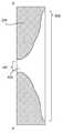
도 5b는 일 실시 예에 따른, 도 5a의 선 A―A´를 따라서 취한 라디칼 반응기의 단면도이다. 라디칼 반응기(136b)는 내부에 배출구(424)가 형성된 몸체(524)를 갖는다. 배출구(424)는 그것의 바닥 부분(520)이 라디칼 반응기(136b)를 가로질러 세로로 연장되는 반면 상부 부분(521)이 파이프(미도시)와의 연결을 위해 좁은 폭을 갖도록 만들어진다. 바닥 부분(520)을 라디칼 반응기(136b)를 가로질러 연장함으로써, 배출구(424)는 과잉 라디칼 또는 기체를 더욱 효율적으로 방출할 수 있다.5B is a cross-sectional view of the radical reactor taken along line A-A 'of FIG. 5A, according to one embodiment. The radical reactor 136b has a
도 6은 일 실시 예에 따른, 도 5a의 선 B―B´를 따라서 취한 라디칼 반응기의 단면도이다. 라디칼 반응기(136)의 몸체(524) 안에서, 플라즈마 챔버들(516, 518)은 혼합 챔버(530)의 오른쪽 면 및 왼쪽 면에 형성된다. 두 개의 플라즈마 챔버들(516, 518) 각각은 홀들(508, 512)을 통해 채널들(502, 506)과 연결되어 기체들을 받고, 슬릿들(604, 608)을 통해 혼합 챔버(530)와 연결된다. 내부 전극들(410, 414)은 라디칼 반응기(137b)를 따라서 세로로 연장된다.6 is a cross-sectional view of the radical reactor taken along the line BB ′ of FIG. 5A, according to one embodiment. In the
도 6의 실시 예에서, 채널(502), 홀(508), 플라즈마 챔버(516) 및 슬릿(604)은 평면 C1―C2를 따라서 정렬된다. 평면 C1―C2는 수직 평면 C1―C4에 대하여 α각도로 기울어진다. 채널(506), 홀(512), 플라즈마 챔버(518) 및 슬릿(608)은 평면 C1―C3를 따라서 정렬된다. 평면 C1―C3는 채널(502), 홀(508), 플라즈마 챔버(516) 및 슬릿(604)과 반대편인 수직 평면 C1―C4에 대하여 β각도로 기울어진다. 각도 α 및 β는 동일하거나 상이한 크기일 수 있다.In the embodiment of FIG. 6,
다른 실시 예에서, 하나 이상의 채널들, 홀들, 플라즈마 챔버들 및 슬릿들이 동일한 평면을 따라 정렬되지 않고, 상이한 배열로 배치될 수 있다. 예를 들어, 채널은 수평적으로 채널의 왼쪽 면 또는 오른쪽 면에서 또는 수직적으로 채널의 위에서 제공될 수 있다. 채널들, 홀들, 플라즈마 챔버들 및 슬릿들의 다양한 다른 배열들이 또한 사용될 수 있다.In another embodiment, one or more channels, holes, plasma chambers and slits may be arranged in a different arrangement, rather than aligned along the same plane. For example, the channel may be provided horizontally on the left or right side of the channel or vertically on top of the channel. Various other arrangements of channels, holes, plasma chambers and slits can also be used.
도 6의 실시 예에서, 제 1 기체는 채널(502) 및 홀(508)을 통해 플라즈마 챔버(516)안으로 주입된다. 내부 전극(410)과 외부 전극(520)을 가로질러 전압을 인가함으로써, 플라즈마가 플라즈마 챔버(516)에서 생성되어, 플라즈마 챔버(516) 내에서 제 1 기체의 라디칼이 생산된다. 제 1 기체의 생성된 라디칼은 그 다음 슬릿(604)를 통해 혼합 챔버(530) 안으로 주입된다. 또한, 제 2 기체가 채널(506) 및 홀(512)을 통해 플라즈마 챔버(518) 안으로 주입된다. 내부 전극(414)과 외부 번극(522)를 가로질러 전압을 인가함으로써, 플라즈마 챔버(518) 내에서 플라즈마가 생성되어, 플라즈마 챔버(518) 내에서 제 2 기체의 라디칼을 생산한다. 제 2 기체의 생성된 라디칼은 그 다음 슬릿(608)을 통해 혼합 챔버(530) 안으로 주입된다.In the embodiment of FIG. 6, the first gas is injected into the
슬릿들(604, 608)은 혼합 챔버(530)의 영역(도 6에서 혼합 챔버(530)의 지점 C1 주변)을 향해 지향되어 혼합 챔버(530) 내의 동일한 영역으로 라디칼들이 주입되도록 한다. 이러한 방식으로, 슬릿들(604, 608)로부터 주입된 라디칼들의 혼합이 용이해 질 수 있다. 즉, 슬릿들(604, 608)은 수직 평면 C1―C4에 대하여 α 각도 및 β 각도들로 기체들의 라디칼이 주입되도록 구성된다. 이러한 방식으로, 양 기체들의 라디칼은 라디칼들이 기판(120)과 접촉하기 전에 혼합 챔버(530) 내에서 효과적으로 혼합된다. 혼합 챔버(530)의 크기는 라디칼들이 기판(120)과 접촉하기 전에 혼합 챔버(530) 내에서 충분히 확산되도록 구성된다. 라디칼들 중 어떤 것은 기판(120)과 접촉하기 전, 접촉하는 동안 또는 접촉한 후에 비활성 상태로 복귀할 수 있다. 남아있는 라디칼 및 복귀된 기체는 배출구(424)를 통해 방출된다.The
아래의 표 1에서 보여지는 것처럼, 상이한 유형의 기체들은 상이한 레벨의 이온화 에너지를 갖는다. 이런 이유로, 플라즈마 챔버에 공급되는 기체의 유형에 따라 상이한 레벨의 전압들이 플라즈마 챔버의 내부 전극과 외부 전극 사이에 인가된다. 상이한 기체들의 라디칼을 생성하기 위해서는, 상이한 기체들에 대한 상이한 레벨의 이온화 에너지들 때문에 상응하는 숫자의 플라즈마 챔버들 및 전극 세트들이 요구될 수 있다.As shown in Table 1 below, different types of gases have different levels of ionization energy. For this reason, different levels of voltage are applied between the inner and outer electrodes of the plasma chamber depending on the type of gas supplied to the plasma chamber. To generate radicals of different gases, corresponding numbers of plasma chambers and electrode sets may be required because of different levels of ionization energies for different gases.

도 6의 실시 예에서, 두 개의 분리된 플라즈마 챔버들(516, 518)이 두 개의 다른 기체들을 받기 위해 제공된다. 플라즈마 챔버(516)과 관련된 전극들(410, 520)에는 플라즈마 챔버(518)과 관련된 전극들(414, 522) 사이의 또 다른 전압 차보다 낮거나 높은 전압 차가 인가될 수 있다. 두 개의 상이한 플라즈마 챔버들(516, 518)을 제공함으로써, 상이한 이온화 에너지를 갖는 두 개의 상이한 기체들의 라디칼이 하나의 라디칼 반응기(138b)에서 생성될 수 있다. 양 플라즈마 챔버(516, 518) 안의 기체들의 다른 조건들(예를 들어, 압력 및 온도)은 원하는 바대로 라디칼을 생성하기 위해 달라질 수 있다.In the embodiment of FIG. 6, two
요약하면, 라디칼 반응기(136b)는 하나의 플라즈마 챔버를 갖는 두 개의 라디칼 반응기들처럼 기능한다. 하나의 라디칼 반응기 안에 두 개의 라디칼 반응기들을 포함함으로써, 선형 증착 장치(100)의 공간 및 비용이 감소될 수 있다.In summary, radical reactor 136b functions like two radical reactors with one plasma chamber. By including two radical reactors in one radical reactor, the space and cost of the
도 7은 또 다른 실시 예에 따른 라디칼 반응기(700)의 단면도이다. 도 7의 라디칼 반응기(700)는 라디칼 반응기(700)의 반대되는 면들에 형성된 두 개의 배출구들(712, 717)을 갖는다. 라디칼 반응기(700)는 채널들(704, 720) 및 홀들(708, 728)을 통해 플라즈마 챔버들(716, 736)에 기체들을 제공하는 채널들(704, 724)을 갖는다. 내부 전극들(712, 732)은 플라즈마 챔버들(716, 736)의 세로 방향을 따라 연장되어, 플라즈마 챔버들(716, 736)을 둘러싸는 외부 전극들과 함께 플라즈마 챔버들(716, 736) 내에서 라디칼을 생성한다. 양 측면에서 배출구들(712, 717)을 제공함으로써, 과잉 기체들 또는 기체의 과잉 라디칼이 라디칼 반응기(700)로부터 보다 효과적으로 방출될 수 있다.7 is a sectional view of a
도 8은 또 다른 실시 예에 따른 라디칼 반응기(800)의 단면도이다. 라디칼 반응기(800)는 채널들(810, 812), 홀들(814, 816), 플라즈마 챔버들(832, 834), 내부 전극들(818, 820) 및 슬릿들(826, 828)이 수직 평면들 D1―D3및 D2―D4를 따라 정렬되는 것을 제외하면 라디칼 반응기(136b)와 유사한 구조를 갖는다. 특히, 채널(810)은 기체원으로부터 제 1 기체를 받고 홀(814)을 통해 플라즈마 챔버(832) 안으로 제 1 기체를 주입한다. 채널(812)는 또 다른 기체원으로부터 제 2 기체를 받고, 홀(816)을 통해 플라즈마 챔버(834) 안으로 제 2 기체를 주입한다.8 is a sectional view of a
제 1 및 제 2 기체들의 라디칼은 내부 전극들(818, 820)과 외부 전극들(822, 824)을 가로질러 전압을 인가함으로써 플라즈마 챔버들(832, 834) 안에서 생성된다. 생성된 라디칼들은 그 다음 슬릿들(822, 824)을 통해서 혼합 챔버(830) 안으로 주입된다. 혼합 챔버(830)는 라디칼이 기판(120) 위에서 혼합 챔버(830) 아래를 이동할 때 라디칼들이 적절히 혼합되기에 충분한 높이를 가질 수 있다. 남아있는 라디칼 또는 기체들은 배출구(842)를 통해 방출된다.Radicals of the first and second gases are generated in the
도 9는 일 실시 예에 따른 라디칼 반응기(900)의 단면도이다. 라디칼 반응기(900)는 채널들(940, 906), 홀들(908, 910), 플라즈마 챔버들(912, 918), 내부 전극들(916, 914) 및 슬릿들(920, 926)의 구성이 라디칼 반응기(136b)의 구성과 유사하다. 그러나, 라디칼 반응기(900)가 라디칼이 혼합되는 분리된 제 1 혼합 챔버(924)를 포함한다는 점에서 라디칼 반응기(900)는 라디칼 반응기(136b)와 상이하다. 혼합된 라디칼은 그 다음 전달 채널(930)을 통해 제 2 혼합 챔버(934) 안으로 주입된다. 혼합된 라디칼은 제 2 혼합 챔버(934) 아래에서 기판(120)과 접촉한다. 기판(120)과 떨어진 분리된 혼합 챔버(924)를 제공함으로써, 라디칼은 기판(120)과 접촉하기 전에 보다 균일하게 혼합된다. 남아있는 라디칼 또는 기체들(비활성 상태로 복귀된)은 라디칼 반응기(900)의 한 측면에 제공된 배출구(902)를 통해 방출된다. 또 다른 실시 예에서, 배출구들은 라디칼 반응기(900)의 양 측면에 형성된다.9 is a cross-sectional view of a
다양한 다른 구성의 라디칼 반응기들이 또한 사용될 수 있다. 도 4 내지 도 9에서 라디칼 반응기의 실시 예들이 두 개의 플라즈마 챔버를 포함함에도 불구하고, 다른 실시 예들은 두 개 이상의 플라즈마 챔버들을 포함할 수 있다. 또한, 플라즈마 챔버들 및 전극들은 원통형 모양과는 다른 모양을 가질 수 있다. 또한, 라디칼 반응기의 상이한 수직 위치들에 위치한 상이한 챔버들을 갖는 것도 가능하다. 나아가, 슬릿들 또는 홀들과는 다른 전달 채널들이 플라즈마 챔버에 연결될 수 있다.Various other configurations of radical reactors may also be used. Although the embodiments of the radical reactor in FIGS. 4 to 9 include two plasma chambers, other embodiments may include two or more plasma chambers. In addition, the plasma chambers and the electrodes may have a different shape than the cylindrical shape. It is also possible to have different chambers located at different vertical positions of the radical reactor. Furthermore, other transmission channels than slits or holes may be connected to the plasma chamber.
도 10은 일 실시 예에 따라, 기판상에 혼합된 라디칼들을 주입하는 공정을 설명하는 순서도이다. 제 1 기체는 기체원과 연결된 채널을 통해 라디칼 반응기 내의 제 1 플라즈마 챔버로 주입된다(1010). 제 1 플라즈마 챔버 내에서, 제 1 기체의 라디칼이 제 1 조건하에서 생성된다(1020). 제 1 조건은 제 1 플라즈마 챔버와 관련된 내부 전극과 외부 전극을 가로질러 제 1 레벨의 전압 차를 인가하는 것을 포함할 수 있다. 제 1 조건은 어떤 범위 내에서 제 1 플라즈마 챔버 안의 플라즈마 또는 기체의 압력과 온도를 유지하는 것을 포함할 수 있다.10 is a flowchart illustrating a process of injecting mixed radicals onto a substrate, according to one embodiment. The first gas is injected 1010 into a first plasma chamber in a radical reactor through a channel connected with a gas source. Within the first plasma chamber, radicals of the first gas are generated 1020 under the first condition. The first condition may include applying a first level of voltage difference across an inner electrode and an outer electrode associated with the first plasma chamber. The first condition may include maintaining the pressure and temperature of the plasma or gas in the first plasma chamber within a range.
제 2 기체는 기체원과 연결된 또 다른 채널을 통해 동일한 라디칼 반응기의 제 2 플라즈마 챔버로 주입된다(1030). 제 2 플라즈마 챔버 내에서, 제 1 기체의 라디칼이 제 2 조건하에서 생성된다(1040). 제 2 조건은 제 2 플라즈마 챔버와 관련된 내부 전극과 외부 전극을 가로질러 제 2 레벨의 전압 차를 인가하는 것을 포함할 수 있다. 제 2 조건은 어떤 범위 내에서 제 2 플라즈마 챔버 안의 플라즈마 또는 기체의 압력과 온도를 유지하는 것을 포함할 수 있다. 제 2 조건의 적어도 하나의 요소는 제 1 조건의 대응되는 요소와 상이하다.The second gas is injected 1030 into a second plasma chamber of the same radical reactor through another channel connected with the gas source. Within the second plasma chamber, radicals of the first gas are generated 1040 under the second condition. The second condition may include applying a second level of voltage difference across the inner electrode and the outer electrode associated with the second plasma chamber. The second condition may include maintaining the pressure and temperature of the plasma or gas in the second plasma chamber within a range. At least one element of the second condition is different from the corresponding element of the first condition.
제 1 및 제 2 플라즈마 챔버들에서 생성된 라디칼은 그 다음 라디칼이 혼합되는 혼합 챔버 안으로 주입된다(1050). 혼합된 라디칼은 그 다음 기판상에 주입된다(1060).Radicals generated in the first and second plasma chambers are then injected 1050 into a mixing chamber where the radicals are mixed. Mixed radicals are then injected 1060 on the substrate.
도 10에서 공정들의 시퀀스(sequence)는 단지 예시적인 것이며, 상이한 시퀀스가 사용될 수 있다. 예를 들어, 제 1 기체를 주입하는 공정(1010)과 제 1 기체의 라디칼을 생성하는 공정(1020)은 동시에 수행될 수 있고, 또는 제 2 기체를 주입하는 공정(1030)과 제 2 기체의 라디칼을 생성하는 공정(1040) 이후에 수행될 수 있다.The sequence of processes in FIG. 10 is merely exemplary and different sequences may be used. For example, the step 1010 of injecting the first gas and the
비록 본 발명이 위에서 몇 가지 실시 예들과 관련하여 상술되었지만, 본 발명의 범위 안에서 다양한 변경들이 이루어질 수 있다. 그러므로, 본 발명에 기재된 내용은 본 발명의 범위를 한정하는 것이 아니라, 예를 들어 설명한 것으로 의도되며, 본 발명의 범위는 이후의 청구항에서 제시된다.Although the invention has been described above in connection with some embodiments above, various changes can be made within the scope of the invention. Therefore, the content described in the present invention is not intended to limit the scope of the present invention, but is intended to be, for example, the scope of the present invention is set forth in the following claims.
Claims (20)
Translated fromKorean상기 제 1 플라즈마 챔버 내에서 연장되는 제 1 내부 전극으로서, 상기 제 1 내부 전극과 제 1 외부 전극을 가로질러 제 1 전압 차를 인가함으로써 상기 제 1 플라즈마 챔버 내에서 상기 제 1 기체의 라디칼을 생성하도록 구성되는 상기 제 1 내부 전극; 및
상기 제 2 플라즈마 챔버 내에서 연장되는 제 2 내부 전극으로서, 상기 제 2 내부 전극과 제 2 외부 전극을 가로질러 제 2 전압 차를 인가함으로써 상기 제 2 플라즈마 챔버 내에서 상기 제 2 기체의 라디칼을 생성하도록 구성되는 상기 제 2 내부 전극을 포함하는, 기판상에 하나 이상의 물질층을 증착하기 위한 라디칼 반응기.A body disposed adjacent to the susceptor on which the substrate is mounted, the body comprising a first plasma chamber configured to receive a first gas, a second plasma chamber configured to receive a second gas, and the first plasma chamber and the second plasma chamber. The body having a mixing chamber connected to receive radicals of the first gas and radicals of the second gas from the first plasma chamber and the second plasma chamber;
A first internal electrode extending in the first plasma chamber, generating radicals of the first gas in the first plasma chamber by applying a first voltage difference across the first internal electrode and the first external electrode. The first internal electrode configured to; And
A second internal electrode extending in the second plasma chamber, generating a radical of the second gas in the second plasma chamber by applying a second voltage difference across the second internal electrode and the second external electrode; And the second internal electrode configured to deposit one or more material layers on a substrate.
상기 몸체에는 상기 제 1 기체의 라디칼과 상기 제 2 기체의 라디칼이 상기 기판과 접촉하기 전에 혼합되는 혼합 챔버가 더 형성된, 기판상에 하나 이상의 물질층을 증착하기 위한 라디칼 반응기.The method of claim 1,
And the body further formed with a mixing chamber in which the radicals of the first gas and the radicals of the second gas are mixed before contacting the substrate.
상기 몸체에는 상기 제 1 플라즈마 챔버를 제 1 기체원에 연결하는 제 1 채널 및 상기 제 2 플라즈마 챔버를 제 2 기체원에 연결하는 제 2 채널이 더 형성된, 기판상에 하나 이상의 물질층을 증착하기 위한 라디칼 반응기.3. The method of claim 2,
Depositing at least one material layer on the substrate further comprising a first channel connecting the first plasma chamber to a first gas source and a second channel connecting the second plasma chamber to a second gas source Radical reactors.
상기 몸체에는 상기 제 1 플라즈마 챔버를 상기 혼합 챔버와 연결하는 적어도 하나의 제 1 천공 및 상기 제 2 플라즈마 챔버를 상기 혼합 챔버와 연결하는 적어도 하나의 제 2 천공이 더 형성된, 기판상에 하나 이상의 물질층을 증착하기 위한 라디칼 반응기.The method of claim 3, wherein
The body further has at least one first perforation connecting the first plasma chamber with the mixing chamber and at least one second perforation connecting the second plasma chamber with the mixing chamber. Radical reactor for depositing layers.
상기 제 1 채널, 상기 제 1 내부 전극, 상기 제 1 플라즈마 챔버 및 상기 제 1 천공은 제 1 평면을 따라서 정렬되고, 상기 제 2 채널, 상기 제 2 내부 전극, 상기 제 2 플라즈마 챔버 및 상기 제 2 천공은 상기 제 1 평면에 대해서 각도를 가지고 지향되는 제 2 평면을 따라서 정렬되는, 기판상에 하나 이상의 물질층을 증착하기 위한 라디칼 반응기.The method of claim 4, wherein
The first channel, the first internal electrode, the first plasma chamber and the first perforation are aligned along a first plane and the second channel, the second internal electrode, the second plasma chamber and the second The perforations are aligned along a second plane oriented at an angle to the first plane, wherein the one or more layers of material are deposited on the substrate.
상기 제 1 천공 및 상기 제 2 천공은 상기 혼합 챔버 내에서 동일한 내부 영역을 향해 지향되는, 기판상에 하나 이상의 물질층을 증착하기 위한 라디칼 반응기.The method of claim 4, wherein
Wherein the first and second perforations are directed towards the same interior region within the mixing chamber.
상기 라디칼 반응기는 상기 서셉터 위에 배치되는, 기판상에 하나 이상의 물질층을 증착하기 위한 라디칼 반응기.The method of claim 1,
And said radical reactor is disposed above said susceptor.
상기 몸체에는 상기 라디칼 반응기의 반대되는 측면들에 있는 두 개의 배출구가 형성된, 기판상에 하나 이상의 물질층을 증착하기 위한 라디칼 반응기.The method of claim 1,
Said body having two outlets on opposite sides of said radical reactor, said radical reactor for depositing one or more layers of material on a substrate.
상기 몸체에는 혼합을 위해 상기 제 1 플라즈마 챔버와 상기 제 2 플라즈마 챔버로부터 상기 제 1 기체의 라디칼과 상기 제 2 기체의 라디칼이 주입되는 제 1 혼합 챔버, 혼합된 라디칼이 상기 기판과 접촉하도록 상기 기판과 마주하는 제 2 혼합 챔버, 및 상기 제 1 혼합 챔버와 상기 제 2 혼합 챔버를 연결하는 전달 채널이 형성된, 기판상에 하나 이상의 물질층을 증착하기 위한 라디칼 반응기.The method of claim 1,
The body includes a first mixing chamber into which radicals of the first gas and radicals of the second gas are injected from the first plasma chamber and the second plasma chamber for mixing, wherein the mixed radicals are in contact with the substrate. And a second mixing chamber facing the surface, and a transfer channel connecting the first mixing chamber and the second mixing chamber.
상기 라디칼 반응기는 기판상에 원자층 증착(Atomic Layer Deposition, ALD)을 수행하기 위해 사용되는 라디칼 반응기.The method of claim 1,
The radical reactor is used to perform atomic layer deposition (ALD) on a substrate.
상기 서셉터와 인접하여 배치되는 몸체로서, 제 1 기체를 받도록 구성되는 제 1 플라즈마 챔버, 제 2 기체를 받도록 구성되는 제 2 플라즈마 챔버, 및 상기 제 1 플라즈마 챔버와 상기 제 2 플라즈마 챔버에 연결되어 상기 제 1 플라즈마 챔버와 상기 제 2 플라즈마 챔버로부터 상기 제 1 기체의 라디칼과 상기 제 2 기체의 라디칼을 받는 혼합 챔버가 형성된 상기 몸체;
상기 제 1 플라즈마 챔버 내에서 연장되는 제 1 내부 전극으로서, 상기 제 1 내부 전극과 제 1 외부 전극을 가로지르는 제 1 전압 차를 인가함으로써 상기 제 1 플라즈마 챔버 내에서 상기 제 1 기체의 라디칼을 생성하도록 구성되는 상기 제 1 내부 전극; 및
상기 제 2 플라즈마 챔버 내에서 연장되는 제 2 내부 전극으로서, 상기 제 2 내부 전극과 제 2 외부 전극을 가로지르는 제 2 전압 차를 인가함으로써 상기 제 2 플라즈마 챔버 내에서 상기 제 2 기체의 라디칼을 생성하도록 구성되는 제 2 내부 전극을 포함하는 라디칼 반응기; 및
상기 서셉터와 상기 라디칼 반응기 사이에 상대적인 움직임을 야기하도록 구성되는 작동기를 포함하는, 원자층 증착을 사용하여 기판상에 하나 이상의 물질층을 증착하기 위한 증착 장치.A susceptor configured to raise the substrate;
A body disposed adjacent to the susceptor, the first plasma chamber configured to receive a first gas, the second plasma chamber configured to receive a second gas, and connected to the first plasma chamber and the second plasma chamber The body having a mixing chamber configured to receive radicals of the first gas and radicals of the second gas from the first plasma chamber and the second plasma chamber;
Generating a radical of the first gas in the first plasma chamber by applying a first voltage difference across the first internal electrode and the first external electrode as a first internal electrode extending in the first plasma chamber The first internal electrode configured to; And
Generating a radical of the second gas in the second plasma chamber by applying a second voltage difference across the second inner electrode and the second outer electrode as a second inner electrode extending in the second plasma chamber; A radical reactor comprising a second internal electrode configured to; And
And an actuator configured to cause relative movement between the susceptor and the radical reactor. 10. A deposition apparatus for depositing one or more layers of material on a substrate using atomic layer deposition.
상기 몸체에는 상기 제 1 기체의 라디칼과 상기 제 2 기체의 라디칼이 상기 기판과 접촉하기 전에 혼합되는 혼합 챔버가 더 형성된, 원자층 증착을 사용하여 기판상에 하나 이상의 물질층을 증착하기 위한 증착 장치.The method of claim 11,
A deposition apparatus for depositing one or more layers of material on the substrate using atomic layer deposition, wherein the body further includes a mixing chamber in which the radicals of the first gas and the radicals of the second gas are mixed before contacting the substrate. .
상기 몸체에는 상기 제 1 플라즈마 챔버를 제 1 기체원에 연결하는 제 1 채널 및 상기 제 2 플라즈마 챔버를 상기 제 2 기체원에 연결하는 제 2 채널가 더 형성된, 원자층 증착을 사용하여 기판상에 하나 이상의 물질층을 증착하기 위한 증착 장치.13. The method of claim 12,
The body further has a first channel connecting the first plasma chamber to a first gas source and a second channel connecting the second plasma chamber to the second gas source, one on the substrate using atomic layer deposition. Deposition apparatus for depositing the above material layer.
상기 몸체에는 상기 제 1 플라즈마 채널을 상기 혼합 챔버와 연결하는 적어도 하나의 제 1 천공 및 상기 제 2 플라즈마 챔버를 상기 혼합 챔버와 연결하는 적어도 하나의 제 2 천공이 더 형성된, 원자층 증착을 사용하여 기판상에 하나 이상의 물질층을 증착하기 위한 증착 장치.The method of claim 13,
The body further comprises at least one first perforation connecting the first plasma channel with the mixing chamber and at least one second perforation connecting the second plasma chamber with the mixing chamber. Deposition apparatus for depositing one or more material layers on a substrate.
상기 제 1 채널, 상기 제 1 내부 전극, 상기 제 1 플라즈마 챔버 및 상기 제 1 천공은 제 1 평면을 따라서 정렬되고, 상기 제 2 채널, 상기 제 2 내부 전극, 상기 제 2 플라즈마 챔버 및 상기 제 2 천공은 상기 제 1 평면에 대해서 각도를 가지고 지향되는 제 2 평면을 따라서 정렬되는, 원자층 증착을 사용하여 기판상에 하나 이상의 물질층을 증착하기 위한 증착 장치.15. The method of claim 14,
The first channel, the first internal electrode, the first plasma chamber and the first perforation are aligned along a first plane and the second channel, the second internal electrode, the second plasma chamber and the second And the perforations are aligned along a second plane oriented at an angle to the first plane, wherein the at least one layer of material is deposited on the substrate using atomic layer deposition.
상기 제 1 천공 및 상기 제 2 천공은 상기 혼합 챔버 내에서 동일한 내부 영역을 향해 지향되는, 원자층 증착을 사용하여 기판상에 하나 이상의 물질층을 증착하기 위한 증착 장치.15. The method of claim 14,
And the first and second apertures are directed towards the same interior region within the mixing chamber.
상기 몸체에는 상기 라디칼 반응기의 반대되는 측면들에 있는 두 개의 배출구가 형성된, 원자층 증착을 사용하여 기판상에 하나 이상의 물질층을 증착하기 위한 증착 장치.The method of claim 11,
Wherein the body is provided with two outlets on opposing sides of the radical reactor. ≪ RTI ID = 0.0 > 18. < / RTI >
상기 몸체에는 혼합을 위해 상기 제 1 플라즈마 챔버와 상기 제 2 플라즈마 챔버로부터 상기 제 1 기체의 라디칼과 상기 제 2 기체의 라디칼이 주입되는 제 1 혼합 챔버, 혼합된 라디칼이 상기 기판과 접촉하도록 상기 기판과 마주하는 제 2 혼합 챔버, 및 상기 제 1 혼합 챔버와 상기 제 2 혼합 챔버를 연결하는 전달 채널이 형성된, 원자층 증착을 사용하여 기판상에 하나 이상의 물질층을 증착하기 위한 증착 장치.The method of claim 11,
The body includes a first mixing chamber into which radicals of the first gas and radicals of the second gas are injected from the first plasma chamber and the second plasma chamber for mixing, wherein the mixed radicals are in contact with the substrate. And a second mixing chamber facing and the transfer channel connecting the first and second mixing chambers to deposit one or more layers of material on the substrate using atomic layer deposition.
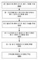
제 1 조건하에 상기 제 1 플라즈마 챔버 안에서 상기 제 1 기체의 라디칼을 생성하는 단계;
상기 라디칼 반응기 안에 형성된 제 2 플라즈마 챔버 안으로 제 2 기체를 주입하는 단계;
상기 제 1 조건과 상이한 제 2 조건하에 상기 제 2 플라즈마 챔버 안에서 상기 제 2 기체의 라디칼을 생성하는 단계;
상기 라디칼 반응기 안에 형성된 혼합 챔버 안에서 상기 제 1 기체의 라디칼과 상기 제 2 기체의 라디칼을 혼합하는 단계; 및
상기 기판상에 상기 혼합된 라디칼을 주입하는 단계를 포함하는, 원자층 증착을 이용하여 기판상에 하나 이상의 층을 증착하는 방법.Injecting a first gas into a first plasma chamber formed in a radical reactor;
Generating radicals of the first gas in the first plasma chamber under a first condition;
Injecting a second gas into a second plasma chamber formed in said radical reactor;
Generating radicals of the second gas in the second plasma chamber under a second condition different from the first condition;
Mixing the radicals of the first gas and the radicals of the second gas in a mixing chamber formed in the radical reactor; And
Injecting the mixed radicals onto the substrate, and depositing one or more layers on the substrate using atomic layer deposition.
상기 제 1 조건은 상기 제 1 플라즈마 챔버의 내부 전극과 외부 전극을 가로질러 제 1 레벨의 전압을 인가하는 것을 포함하고, 상기 제 2 조건은 상기 제 2 플라즈마 챔버의 내부 전극과 외부 전극을 가로질러 제 2 레벨의 전압을 인가하는 것을 포함하는, 원자층 증착을 이용하여 기판상에 하나 이상의 층을 증착하는 방법.The method of claim 19,
The first condition includes applying a first level of voltage across the inner and outer electrodes of the first plasma chamber, and the second condition is across the inner and outer electrodes of the second plasma chamber. A method of depositing one or more layers on a substrate using atomic layer deposition, comprising applying a second level of voltage.
Applications Claiming Priority (3)
| Application Number | Priority Date | Filing Date | Title |
|---|---|---|---|
| US41079610P | 2010-11-05 | 2010-11-05 | |
| US61/410,796 | 2010-11-05 | ||
| PCT/US2011/058552WO2012061278A1 (en) | 2010-11-05 | 2011-10-31 | Radical reactor with multiple plasma chambers |
Related Child Applications (1)
| Application Number | Title | Priority Date | Filing Date |
|---|---|---|---|
| KR1020147029856ADivisionKR20140138328A (en) | 2010-11-05 | 2011-10-31 | Radical reactor with multiple plasma chambers |
Publications (1)
| Publication Number | Publication Date |
|---|---|
| KR20130086620Atrue KR20130086620A (en) | 2013-08-02 |
Family
ID=46019883
Family Applications (2)
| Application Number | Title | Priority Date | Filing Date |
|---|---|---|---|
| KR1020137013917ACeasedKR20130086620A (en) | 2010-11-05 | 2011-10-31 | Radical reactor with multiple plasma chambers |
| KR1020147029856ACeasedKR20140138328A (en) | 2010-11-05 | 2011-10-31 | Radical reactor with multiple plasma chambers |
Family Applications After (1)
| Application Number | Title | Priority Date | Filing Date |
|---|---|---|---|
| KR1020147029856ACeasedKR20140138328A (en) | 2010-11-05 | 2011-10-31 | Radical reactor with multiple plasma chambers |
Country Status (5)
| Country | Link |
|---|---|
| US (1) | US20120114877A1 (en) |
| KR (2) | KR20130086620A (en) |
| CN (1) | CN103201408A (en) |
| TW (1) | TW201229302A (en) |
| WO (1) | WO2012061278A1 (en) |
Families Citing this family (430)
| Publication number | Priority date | Publication date | Assignee | Title |
|---|---|---|---|---|
| US8986456B2 (en) | 2006-10-10 | 2015-03-24 | Asm America, Inc. | Precursor delivery system |
| US20100037820A1 (en)* | 2008-08-13 | 2010-02-18 | Synos Technology, Inc. | Vapor Deposition Reactor |
| US20100037824A1 (en)* | 2008-08-13 | 2010-02-18 | Synos Technology, Inc. | Plasma Reactor Having Injector |
| US8770142B2 (en)* | 2008-09-17 | 2014-07-08 | Veeco Ald Inc. | Electrode for generating plasma and plasma generator |
| US8851012B2 (en)* | 2008-09-17 | 2014-10-07 | Veeco Ald Inc. | Vapor deposition reactor using plasma and method for forming thin film using the same |
| US10378106B2 (en) | 2008-11-14 | 2019-08-13 | Asm Ip Holding B.V. | Method of forming insulation film by modified PEALD |
| US8871628B2 (en)* | 2009-01-21 | 2014-10-28 | Veeco Ald Inc. | Electrode structure, device comprising the same and method for forming electrode structure |
| US8257799B2 (en) | 2009-02-23 | 2012-09-04 | Synos Technology, Inc. | Method for forming thin film using radicals generated by plasma |
| US9394608B2 (en) | 2009-04-06 | 2016-07-19 | Asm America, Inc. | Semiconductor processing reactor and components thereof |
| US8758512B2 (en)* | 2009-06-08 | 2014-06-24 | Veeco Ald Inc. | Vapor deposition reactor and method for forming thin film |
| US8802201B2 (en) | 2009-08-14 | 2014-08-12 | Asm America, Inc. | Systems and methods for thin-film deposition of metal oxides using excited nitrogen-oxygen species |
| JP5648349B2 (en)* | 2009-09-17 | 2015-01-07 | 東京エレクトロン株式会社 | Deposition equipment |
| KR101775608B1 (en) | 2010-01-21 | 2017-09-19 | 파워다인, 인코포레이티드 | Generating steam from carbonaceous material |
| US8771791B2 (en) | 2010-10-18 | 2014-07-08 | Veeco Ald Inc. | Deposition of layer using depositing apparatus with reciprocating susceptor |
| US8877300B2 (en) | 2011-02-16 | 2014-11-04 | Veeco Ald Inc. | Atomic layer deposition using radicals of gas mixture |
| US9163310B2 (en) | 2011-02-18 | 2015-10-20 | Veeco Ald Inc. | Enhanced deposition of layer on substrate using radicals |
| US9312155B2 (en) | 2011-06-06 | 2016-04-12 | Asm Japan K.K. | High-throughput semiconductor-processing apparatus equipped with multiple dual-chamber modules |
| US9793148B2 (en) | 2011-06-22 | 2017-10-17 | Asm Japan K.K. | Method for positioning wafers in multiple wafer transport |
| US10364496B2 (en) | 2011-06-27 | 2019-07-30 | Asm Ip Holding B.V. | Dual section module having shared and unshared mass flow controllers |
| US10854498B2 (en) | 2011-07-15 | 2020-12-01 | Asm Ip Holding B.V. | Wafer-supporting device and method for producing same |
| US20130023129A1 (en) | 2011-07-20 | 2013-01-24 | Asm America, Inc. | Pressure transmitter for a semiconductor processing environment |
| US9341296B2 (en) | 2011-10-27 | 2016-05-17 | Asm America, Inc. | Heater jacket for a fluid line |
| US9096931B2 (en) | 2011-10-27 | 2015-08-04 | Asm America, Inc | Deposition valve assembly and method of heating the same |
| US9017481B1 (en) | 2011-10-28 | 2015-04-28 | Asm America, Inc. | Process feed management for semiconductor substrate processing |
| US9005539B2 (en) | 2011-11-23 | 2015-04-14 | Asm Ip Holding B.V. | Chamber sealing member |
| US9167625B2 (en) | 2011-11-23 | 2015-10-20 | Asm Ip Holding B.V. | Radiation shielding for a substrate holder |
| US9202727B2 (en) | 2012-03-02 | 2015-12-01 | ASM IP Holding | Susceptor heater shim |
| KR101929481B1 (en) | 2012-03-26 | 2018-12-14 | 주성엔지니어링(주) | Substrate processing apparatus and substrate processing method |
| US8946830B2 (en) | 2012-04-04 | 2015-02-03 | Asm Ip Holdings B.V. | Metal oxide protective layer for a semiconductor device |
| TWI622664B (en) | 2012-05-02 | 2018-05-01 | Asm智慧財產控股公司 | Phase stable film, structure and device comprising the same, and method of forming same |
| US8728832B2 (en) | 2012-05-07 | 2014-05-20 | Asm Ip Holdings B.V. | Semiconductor device dielectric interface layer |
| KR102029952B1 (en)* | 2012-05-29 | 2019-10-08 | 주성엔지니어링(주) | Apparatus and Method of processing substrate |
| WO2013180453A1 (en)* | 2012-05-29 | 2013-12-05 | 주성엔지니어링(주) | Substrate processing device and substrate processing method |
| KR102002042B1 (en)* | 2012-05-29 | 2019-07-19 | 주성엔지니어링(주) | Substrate processing apparatus and substrate processing method |
| KR102014877B1 (en)* | 2012-05-30 | 2019-08-27 | 주성엔지니어링(주) | Substrate processing apparatus and substrate processing method |
| US8933375B2 (en) | 2012-06-27 | 2015-01-13 | Asm Ip Holding B.V. | Susceptor heater and method of heating a substrate |
| US9558931B2 (en) | 2012-07-27 | 2017-01-31 | Asm Ip Holding B.V. | System and method for gas-phase sulfur passivation of a semiconductor surface |
| US9117866B2 (en) | 2012-07-31 | 2015-08-25 | Asm Ip Holding B.V. | Apparatus and method for calculating a wafer position in a processing chamber under process conditions |
| US9169975B2 (en) | 2012-08-28 | 2015-10-27 | Asm Ip Holding B.V. | Systems and methods for mass flow controller verification |
| US9659799B2 (en) | 2012-08-28 | 2017-05-23 | Asm Ip Holding B.V. | Systems and methods for dynamic semiconductor process scheduling |
| WO2014039695A1 (en) | 2012-09-05 | 2014-03-13 | Powerdyne, Inc. | Methods for generating hydrogen gas using plasma sources |
| US9410452B2 (en) | 2012-09-05 | 2016-08-09 | Powerdyne, Inc. | Fuel generation using high-voltage electric fields methods |
| US9273570B2 (en) | 2012-09-05 | 2016-03-01 | Powerdyne, Inc. | Methods for power generation from H2O, CO2, O2 and a carbon feed stock |
| KR20150053779A (en) | 2012-09-05 | 2015-05-18 | 파워다인, 인코포레이티드 | Method for sequestering heavy metal particulates using h2o, co2, o2, and a source of particulates |
| HK1212437A1 (en) | 2012-09-05 | 2016-06-10 | Powerdyne, Inc. | Fuel generation using high-voltage electric fields methods |
| US9561486B2 (en) | 2012-09-05 | 2017-02-07 | Powerdyne, Inc. | System for generating fuel materials using Fischer-Tropsch catalysts and plasma sources |
| HK1212438A1 (en) | 2012-09-05 | 2016-06-10 | Powerdyne, Inc. | Fuel generation using high-voltage electric fields methods |
| KR101929473B1 (en)* | 2012-09-10 | 2019-03-12 | 주성엔지니어링(주) | Apparatus and method of processing substrate |
| US9021985B2 (en) | 2012-09-12 | 2015-05-05 | Asm Ip Holdings B.V. | Process gas management for an inductively-coupled plasma deposition reactor |
| US9324811B2 (en) | 2012-09-26 | 2016-04-26 | Asm Ip Holding B.V. | Structures and devices including a tensile-stressed silicon arsenic layer and methods of forming same |
| US10714315B2 (en) | 2012-10-12 | 2020-07-14 | Asm Ip Holdings B.V. | Semiconductor reaction chamber showerhead |
| US9640416B2 (en) | 2012-12-26 | 2017-05-02 | Asm Ip Holding B.V. | Single-and dual-chamber module-attachable wafer-handling chamber |
| US20140205769A1 (en)* | 2013-01-22 | 2014-07-24 | Veeco Ald Inc. | Cascaded plasma reactor |
| US20160376700A1 (en) | 2013-02-01 | 2016-12-29 | Asm Ip Holding B.V. | System for treatment of deposition reactor |
| US8894870B2 (en) | 2013-02-01 | 2014-11-25 | Asm Ip Holding B.V. | Multi-step method and apparatus for etching compounds containing a metal |
| US9484191B2 (en) | 2013-03-08 | 2016-11-01 | Asm Ip Holding B.V. | Pulsed remote plasma method and system |
| US9589770B2 (en) | 2013-03-08 | 2017-03-07 | Asm Ip Holding B.V. | Method and systems for in-situ formation of intermediate reactive species |
| US8993054B2 (en) | 2013-07-12 | 2015-03-31 | Asm Ip Holding B.V. | Method and system to reduce outgassing in a reaction chamber |
| US9018111B2 (en)* | 2013-07-22 | 2015-04-28 | Asm Ip Holding B.V. | Semiconductor reaction chamber with plasma capabilities |
| US9396934B2 (en) | 2013-08-14 | 2016-07-19 | Asm Ip Holding B.V. | Methods of forming films including germanium tin and structures and devices including the films |
| US9793115B2 (en) | 2013-08-14 | 2017-10-17 | Asm Ip Holding B.V. | Structures and devices including germanium-tin films and methods of forming same |
| US9240412B2 (en) | 2013-09-27 | 2016-01-19 | Asm Ip Holding B.V. | Semiconductor structure and device and methods of forming same using selective epitaxial process |
| US9556516B2 (en) | 2013-10-09 | 2017-01-31 | ASM IP Holding B.V | Method for forming Ti-containing film by PEALD using TDMAT or TDEAT |
| US9605343B2 (en) | 2013-11-13 | 2017-03-28 | Asm Ip Holding B.V. | Method for forming conformal carbon films, structures conformal carbon film, and system of forming same |
| US10179947B2 (en) | 2013-11-26 | 2019-01-15 | Asm Ip Holding B.V. | Method for forming conformal nitrided, oxidized, or carbonized dielectric film by atomic layer deposition |
| WO2015089069A1 (en)* | 2013-12-09 | 2015-06-18 | Powerdyne, Inc. | Systems and methods of plasma partial dissociation of carbon dioxide, water, and carbonaceous matter |
| US10683571B2 (en) | 2014-02-25 | 2020-06-16 | Asm Ip Holding B.V. | Gas supply manifold and method of supplying gases to chamber using same |
| US10167557B2 (en) | 2014-03-18 | 2019-01-01 | Asm Ip Holding B.V. | Gas distribution system, reactor including the system, and methods of using the same |
| US9447498B2 (en) | 2014-03-18 | 2016-09-20 | Asm Ip Holding B.V. | Method for performing uniform processing in gas system-sharing multiple reaction chambers |
| US11015245B2 (en) | 2014-03-19 | 2021-05-25 | Asm Ip Holding B.V. | Gas-phase reactor and system having exhaust plenum and components thereof |
| US9404587B2 (en) | 2014-04-24 | 2016-08-02 | ASM IP Holding B.V | Lockout tagout for semiconductor vacuum valve |
| US10858737B2 (en) | 2014-07-28 | 2020-12-08 | Asm Ip Holding B.V. | Showerhead assembly and components thereof |
| US9543180B2 (en) | 2014-08-01 | 2017-01-10 | Asm Ip Holding B.V. | Apparatus and method for transporting wafers between wafer carrier and process tool under vacuum |
| US9890456B2 (en) | 2014-08-21 | 2018-02-13 | Asm Ip Holding B.V. | Method and system for in situ formation of gas-phase compounds |
| US10941490B2 (en) | 2014-10-07 | 2021-03-09 | Asm Ip Holding B.V. | Multiple temperature range susceptor, assembly, reactor and system including the susceptor, and methods of using the same |
| US9657845B2 (en) | 2014-10-07 | 2017-05-23 | Asm Ip Holding B.V. | Variable conductance gas distribution apparatus and method |
| KR102300403B1 (en) | 2014-11-19 | 2021-09-09 | 에이에스엠 아이피 홀딩 비.브이. | Method of depositing thin film |
| KR102263121B1 (en) | 2014-12-22 | 2021-06-09 | 에이에스엠 아이피 홀딩 비.브이. | Semiconductor device and manufacuring method thereof |
| US9478415B2 (en) | 2015-02-13 | 2016-10-25 | Asm Ip Holding B.V. | Method for forming film having low resistance and shallow junction depth |
| US10529542B2 (en) | 2015-03-11 | 2020-01-07 | Asm Ip Holdings B.V. | Cross-flow reactor and method |
| US10276355B2 (en) | 2015-03-12 | 2019-04-30 | Asm Ip Holding B.V. | Multi-zone reactor, system including the reactor, and method of using the same |
| US10458018B2 (en) | 2015-06-26 | 2019-10-29 | Asm Ip Holding B.V. | Structures including metal carbide material, devices including the structures, and methods of forming same |
| US10600673B2 (en) | 2015-07-07 | 2020-03-24 | Asm Ip Holding B.V. | Magnetic susceptor to baseplate seal |
| US9899291B2 (en) | 2015-07-13 | 2018-02-20 | Asm Ip Holding B.V. | Method for protecting layer by forming hydrocarbon-based extremely thin film |
| US10043661B2 (en) | 2015-07-13 | 2018-08-07 | Asm Ip Holding B.V. | Method for protecting layer by forming hydrocarbon-based extremely thin film |
| US10083836B2 (en) | 2015-07-24 | 2018-09-25 | Asm Ip Holding B.V. | Formation of boron-doped titanium metal films with high work function |
| US10087525B2 (en) | 2015-08-04 | 2018-10-02 | Asm Ip Holding B.V. | Variable gap hard stop design |
| US9647114B2 (en) | 2015-08-14 | 2017-05-09 | Asm Ip Holding B.V. | Methods of forming highly p-type doped germanium tin films and structures and devices including the films |
| US9711345B2 (en) | 2015-08-25 | 2017-07-18 | Asm Ip Holding B.V. | Method for forming aluminum nitride-based film by PEALD |
| US10550469B2 (en)* | 2015-09-04 | 2020-02-04 | Lam Research Corporation | Plasma excitation for spatial atomic layer deposition (ALD) reactors |
| US9960072B2 (en) | 2015-09-29 | 2018-05-01 | Asm Ip Holding B.V. | Variable adjustment for precise matching of multiple chamber cavity housings |
| US9909214B2 (en) | 2015-10-15 | 2018-03-06 | Asm Ip Holding B.V. | Method for depositing dielectric film in trenches by PEALD |
| US10211308B2 (en) | 2015-10-21 | 2019-02-19 | Asm Ip Holding B.V. | NbMC layers |
| US10322384B2 (en) | 2015-11-09 | 2019-06-18 | Asm Ip Holding B.V. | Counter flow mixer for process chamber |
| US9455138B1 (en) | 2015-11-10 | 2016-09-27 | Asm Ip Holding B.V. | Method for forming dielectric film in trenches by PEALD using H-containing gas |
| US9905420B2 (en) | 2015-12-01 | 2018-02-27 | Asm Ip Holding B.V. | Methods of forming silicon germanium tin films and structures and devices including the films |
| US9607837B1 (en) | 2015-12-21 | 2017-03-28 | Asm Ip Holding B.V. | Method for forming silicon oxide cap layer for solid state diffusion process |
| US9627221B1 (en) | 2015-12-28 | 2017-04-18 | Asm Ip Holding B.V. | Continuous process incorporating atomic layer etching |
| US9735024B2 (en) | 2015-12-28 | 2017-08-15 | Asm Ip Holding B.V. | Method of atomic layer etching using functional group-containing fluorocarbon |
| US11139308B2 (en) | 2015-12-29 | 2021-10-05 | Asm Ip Holding B.V. | Atomic layer deposition of III-V compounds to form V-NAND devices |
| US10529554B2 (en) | 2016-02-19 | 2020-01-07 | Asm Ip Holding B.V. | Method for forming silicon nitride film selectively on sidewalls or flat surfaces of trenches |
| US10468251B2 (en) | 2016-02-19 | 2019-11-05 | Asm Ip Holding B.V. | Method for forming spacers using silicon nitride film for spacer-defined multiple patterning |
| US9754779B1 (en) | 2016-02-19 | 2017-09-05 | Asm Ip Holding B.V. | Method for forming silicon nitride film selectively on sidewalls or flat surfaces of trenches |
| US10501866B2 (en) | 2016-03-09 | 2019-12-10 | Asm Ip Holding B.V. | Gas distribution apparatus for improved film uniformity in an epitaxial system |
| US10343920B2 (en) | 2016-03-18 | 2019-07-09 | Asm Ip Holding B.V. | Aligned carbon nanotubes |
| US9892913B2 (en) | 2016-03-24 | 2018-02-13 | Asm Ip Holding B.V. | Radial and thickness control via biased multi-port injection settings |
| US10190213B2 (en) | 2016-04-21 | 2019-01-29 | Asm Ip Holding B.V. | Deposition of metal borides |
| US10087522B2 (en) | 2016-04-21 | 2018-10-02 | Asm Ip Holding B.V. | Deposition of metal borides |
| US10865475B2 (en) | 2016-04-21 | 2020-12-15 | Asm Ip Holding B.V. | Deposition of metal borides and silicides |
| US10367080B2 (en) | 2016-05-02 | 2019-07-30 | Asm Ip Holding B.V. | Method of forming a germanium oxynitride film |
| US10032628B2 (en) | 2016-05-02 | 2018-07-24 | Asm Ip Holding B.V. | Source/drain performance through conformal solid state doping |
| KR102592471B1 (en) | 2016-05-17 | 2023-10-20 | 에이에스엠 아이피 홀딩 비.브이. | Method of forming metal interconnection and method of fabricating semiconductor device using the same |
| US11453943B2 (en) | 2016-05-25 | 2022-09-27 | Asm Ip Holding B.V. | Method for forming carbon-containing silicon/metal oxide or nitride film by ALD using silicon precursor and hydrocarbon precursor |
| US10388509B2 (en) | 2016-06-28 | 2019-08-20 | Asm Ip Holding B.V. | Formation of epitaxial layers via dislocation filtering |
| US10612137B2 (en) | 2016-07-08 | 2020-04-07 | Asm Ip Holdings B.V. | Organic reactants for atomic layer deposition |
| US9859151B1 (en) | 2016-07-08 | 2018-01-02 | Asm Ip Holding B.V. | Selective film deposition method to form air gaps |
| US9793135B1 (en) | 2016-07-14 | 2017-10-17 | ASM IP Holding B.V | Method of cyclic dry etching using etchant film |
| US10714385B2 (en) | 2016-07-19 | 2020-07-14 | Asm Ip Holding B.V. | Selective deposition of tungsten |
| KR102354490B1 (en) | 2016-07-27 | 2022-01-21 | 에이에스엠 아이피 홀딩 비.브이. | Method of processing a substrate |
| US10177025B2 (en) | 2016-07-28 | 2019-01-08 | Asm Ip Holding B.V. | Method and apparatus for filling a gap |
| KR102532607B1 (en) | 2016-07-28 | 2023-05-15 | 에이에스엠 아이피 홀딩 비.브이. | Substrate processing apparatus and method of operating the same |
| US10395919B2 (en) | 2016-07-28 | 2019-08-27 | Asm Ip Holding B.V. | Method and apparatus for filling a gap |
| US9887082B1 (en) | 2016-07-28 | 2018-02-06 | Asm Ip Holding B.V. | Method and apparatus for filling a gap |
| US9812320B1 (en) | 2016-07-28 | 2017-11-07 | Asm Ip Holding B.V. | Method and apparatus for filling a gap |
| US10090316B2 (en) | 2016-09-01 | 2018-10-02 | Asm Ip Holding B.V. | 3D stacked multilayer semiconductor memory using doped select transistor channel |
| US10410943B2 (en) | 2016-10-13 | 2019-09-10 | Asm Ip Holding B.V. | Method for passivating a surface of a semiconductor and related systems |
| US10643826B2 (en) | 2016-10-26 | 2020-05-05 | Asm Ip Holdings B.V. | Methods for thermally calibrating reaction chambers |
| US11532757B2 (en) | 2016-10-27 | 2022-12-20 | Asm Ip Holding B.V. | Deposition of charge trapping layers |
| US10714350B2 (en) | 2016-11-01 | 2020-07-14 | ASM IP Holdings, B.V. | Methods for forming a transition metal niobium nitride film on a substrate by atomic layer deposition and related semiconductor device structures |
| US10229833B2 (en) | 2016-11-01 | 2019-03-12 | Asm Ip Holding B.V. | Methods for forming a transition metal nitride film on a substrate by atomic layer deposition and related semiconductor device structures |
| US10643904B2 (en) | 2016-11-01 | 2020-05-05 | Asm Ip Holdings B.V. | Methods for forming a semiconductor device and related semiconductor device structures |
| US10435790B2 (en) | 2016-11-01 | 2019-10-08 | Asm Ip Holding B.V. | Method of subatmospheric plasma-enhanced ALD using capacitively coupled electrodes with narrow gap |
| US10134757B2 (en) | 2016-11-07 | 2018-11-20 | Asm Ip Holding B.V. | Method of processing a substrate and a device manufactured by using the method |
| KR102546317B1 (en) | 2016-11-15 | 2023-06-21 | 에이에스엠 아이피 홀딩 비.브이. | Gas supply unit and substrate processing apparatus including the same |
| US10340135B2 (en) | 2016-11-28 | 2019-07-02 | Asm Ip Holding B.V. | Method of topologically restricted plasma-enhanced cyclic deposition of silicon or metal nitride |
| KR102762543B1 (en) | 2016-12-14 | 2025-02-05 | 에이에스엠 아이피 홀딩 비.브이. | Substrate processing apparatus |
| US9916980B1 (en) | 2016-12-15 | 2018-03-13 | Asm Ip Holding B.V. | Method of forming a structure on a substrate |
| US11581186B2 (en) | 2016-12-15 | 2023-02-14 | Asm Ip Holding B.V. | Sequential infiltration synthesis apparatus |
| US11447861B2 (en) | 2016-12-15 | 2022-09-20 | Asm Ip Holding B.V. | Sequential infiltration synthesis apparatus and a method of forming a patterned structure |
| KR102700194B1 (en) | 2016-12-19 | 2024-08-28 | 에이에스엠 아이피 홀딩 비.브이. | Substrate processing apparatus |
| US10269558B2 (en) | 2016-12-22 | 2019-04-23 | Asm Ip Holding B.V. | Method of forming a structure on a substrate |
| US10867788B2 (en) | 2016-12-28 | 2020-12-15 | Asm Ip Holding B.V. | Method of forming a structure on a substrate |
| US11390950B2 (en) | 2017-01-10 | 2022-07-19 | Asm Ip Holding B.V. | Reactor system and method to reduce residue buildup during a film deposition process |
| US10655221B2 (en) | 2017-02-09 | 2020-05-19 | Asm Ip Holding B.V. | Method for depositing oxide film by thermal ALD and PEALD |
| US10468261B2 (en) | 2017-02-15 | 2019-11-05 | Asm Ip Holding B.V. | Methods for forming a metallic film on a substrate by cyclical deposition and related semiconductor device structures |
| US10529563B2 (en) | 2017-03-29 | 2020-01-07 | Asm Ip Holdings B.V. | Method for forming doped metal oxide films on a substrate by cyclical deposition and related semiconductor device structures |
| US10283353B2 (en) | 2017-03-29 | 2019-05-07 | Asm Ip Holding B.V. | Method of reforming insulating film deposited on substrate with recess pattern |
| US10103040B1 (en) | 2017-03-31 | 2018-10-16 | Asm Ip Holding B.V. | Apparatus and method for manufacturing a semiconductor device |
| USD830981S1 (en) | 2017-04-07 | 2018-10-16 | Asm Ip Holding B.V. | Susceptor for semiconductor substrate processing apparatus |
| KR102457289B1 (en) | 2017-04-25 | 2022-10-21 | 에이에스엠 아이피 홀딩 비.브이. | Method for depositing a thin film and manufacturing a semiconductor device |
| US10770286B2 (en) | 2017-05-08 | 2020-09-08 | Asm Ip Holdings B.V. | Methods for selectively forming a silicon nitride film on a substrate and related semiconductor device structures |
| US10892156B2 (en) | 2017-05-08 | 2021-01-12 | Asm Ip Holding B.V. | Methods for forming a silicon nitride film on a substrate and related semiconductor device structures |
| US10446393B2 (en) | 2017-05-08 | 2019-10-15 | Asm Ip Holding B.V. | Methods for forming silicon-containing epitaxial layers and related semiconductor device structures |
| US10504742B2 (en) | 2017-05-31 | 2019-12-10 | Asm Ip Holding B.V. | Method of atomic layer etching using hydrogen plasma |
| US10886123B2 (en) | 2017-06-02 | 2021-01-05 | Asm Ip Holding B.V. | Methods for forming low temperature semiconductor layers and related semiconductor device structures |
| US12040200B2 (en) | 2017-06-20 | 2024-07-16 | Asm Ip Holding B.V. | Semiconductor processing apparatus and methods for calibrating a semiconductor processing apparatus |
| US11306395B2 (en) | 2017-06-28 | 2022-04-19 | Asm Ip Holding B.V. | Methods for depositing a transition metal nitride film on a substrate by atomic layer deposition and related deposition apparatus |
| US10685834B2 (en) | 2017-07-05 | 2020-06-16 | Asm Ip Holdings B.V. | Methods for forming a silicon germanium tin layer and related semiconductor device structures |
| KR20190009245A (en) | 2017-07-18 | 2019-01-28 | 에이에스엠 아이피 홀딩 비.브이. | Methods for forming a semiconductor device structure and related semiconductor device structures |
| US11374112B2 (en) | 2017-07-19 | 2022-06-28 | Asm Ip Holding B.V. | Method for depositing a group IV semiconductor and related semiconductor device structures |
| US11018002B2 (en) | 2017-07-19 | 2021-05-25 | Asm Ip Holding B.V. | Method for selectively depositing a Group IV semiconductor and related semiconductor device structures |
| US10541333B2 (en) | 2017-07-19 | 2020-01-21 | Asm Ip Holding B.V. | Method for depositing a group IV semiconductor and related semiconductor device structures |
| US10605530B2 (en) | 2017-07-26 | 2020-03-31 | Asm Ip Holding B.V. | Assembly of a liner and a flange for a vertical furnace as well as the liner and the vertical furnace |
| US10312055B2 (en) | 2017-07-26 | 2019-06-04 | Asm Ip Holding B.V. | Method of depositing film by PEALD using negative bias |
| US10590535B2 (en) | 2017-07-26 | 2020-03-17 | Asm Ip Holdings B.V. | Chemical treatment, deposition and/or infiltration apparatus and method for using the same |
| TWI815813B (en) | 2017-08-04 | 2023-09-21 | 荷蘭商Asm智慧財產控股公司 | Showerhead assembly for distributing a gas within a reaction chamber |
| US10692741B2 (en) | 2017-08-08 | 2020-06-23 | Asm Ip Holdings B.V. | Radiation shield |
| US10770336B2 (en) | 2017-08-08 | 2020-09-08 | Asm Ip Holding B.V. | Substrate lift mechanism and reactor including same |
| US11139191B2 (en) | 2017-08-09 | 2021-10-05 | Asm Ip Holding B.V. | Storage apparatus for storing cassettes for substrates and processing apparatus equipped therewith |
| US11769682B2 (en) | 2017-08-09 | 2023-09-26 | Asm Ip Holding B.V. | Storage apparatus for storing cassettes for substrates and processing apparatus equipped therewith |
| US10249524B2 (en) | 2017-08-09 | 2019-04-02 | Asm Ip Holding B.V. | Cassette holder assembly for a substrate cassette and holding member for use in such assembly |
| US10236177B1 (en) | 2017-08-22 | 2019-03-19 | ASM IP Holding B.V.. | Methods for depositing a doped germanium tin semiconductor and related semiconductor device structures |
| USD900036S1 (en) | 2017-08-24 | 2020-10-27 | Asm Ip Holding B.V. | Heater electrical connector and adapter |
| US11830730B2 (en) | 2017-08-29 | 2023-11-28 | Asm Ip Holding B.V. | Layer forming method and apparatus |
| US11056344B2 (en) | 2017-08-30 | 2021-07-06 | Asm Ip Holding B.V. | Layer forming method |
| KR102491945B1 (en) | 2017-08-30 | 2023-01-26 | 에이에스엠 아이피 홀딩 비.브이. | Substrate processing apparatus |
| US11295980B2 (en) | 2017-08-30 | 2022-04-05 | Asm Ip Holding B.V. | Methods for depositing a molybdenum metal film over a dielectric surface of a substrate by a cyclical deposition process and related semiconductor device structures |
| KR102401446B1 (en) | 2017-08-31 | 2022-05-24 | 에이에스엠 아이피 홀딩 비.브이. | Substrate processing apparatus |
| US10607895B2 (en) | 2017-09-18 | 2020-03-31 | Asm Ip Holdings B.V. | Method for forming a semiconductor device structure comprising a gate fill metal |
| KR102630301B1 (en) | 2017-09-21 | 2024-01-29 | 에이에스엠 아이피 홀딩 비.브이. | Method of sequential infiltration synthesis treatment of infiltrateable material and structures and devices formed using same |
| US10844484B2 (en) | 2017-09-22 | 2020-11-24 | Asm Ip Holding B.V. | Apparatus for dispensing a vapor phase reactant to a reaction chamber and related methods |
| US10658205B2 (en) | 2017-09-28 | 2020-05-19 | Asm Ip Holdings B.V. | Chemical dispensing apparatus and methods for dispensing a chemical to a reaction chamber |
| US10403504B2 (en) | 2017-10-05 | 2019-09-03 | Asm Ip Holding B.V. | Method for selectively depositing a metallic film on a substrate |
| US10319588B2 (en) | 2017-10-10 | 2019-06-11 | Asm Ip Holding B.V. | Method for depositing a metal chalcogenide on a substrate by cyclical deposition |
| US10923344B2 (en) | 2017-10-30 | 2021-02-16 | Asm Ip Holding B.V. | Methods for forming a semiconductor structure and related semiconductor structures |
| KR102443047B1 (en) | 2017-11-16 | 2022-09-14 | 에이에스엠 아이피 홀딩 비.브이. | Method of processing a substrate and a device manufactured by the same |
| US10910262B2 (en) | 2017-11-16 | 2021-02-02 | Asm Ip Holding B.V. | Method of selectively depositing a capping layer structure on a semiconductor device structure |
| US11022879B2 (en) | 2017-11-24 | 2021-06-01 | Asm Ip Holding B.V. | Method of forming an enhanced unexposed photoresist layer |
| CN111344522B (en) | 2017-11-27 | 2022-04-12 | 阿斯莫Ip控股公司 | Including clean mini-environment device |
| WO2019103613A1 (en) | 2017-11-27 | 2019-05-31 | Asm Ip Holding B.V. | A storage device for storing wafer cassettes for use with a batch furnace |
| US10290508B1 (en) | 2017-12-05 | 2019-05-14 | Asm Ip Holding B.V. | Method for forming vertical spacers for spacer-defined patterning |
| US10872771B2 (en) | 2018-01-16 | 2020-12-22 | Asm Ip Holding B. V. | Method for depositing a material film on a substrate within a reaction chamber by a cyclical deposition process and related device structures |
| KR102695659B1 (en) | 2018-01-19 | 2024-08-14 | 에이에스엠 아이피 홀딩 비.브이. | Method for depositing a gap filling layer by plasma assisted deposition |
| TWI799494B (en) | 2018-01-19 | 2023-04-21 | 荷蘭商Asm 智慧財產控股公司 | Deposition method |
| USD903477S1 (en) | 2018-01-24 | 2020-12-01 | Asm Ip Holdings B.V. | Metal clamp |
| US11018047B2 (en) | 2018-01-25 | 2021-05-25 | Asm Ip Holding B.V. | Hybrid lift pin |
| USD880437S1 (en) | 2018-02-01 | 2020-04-07 | Asm Ip Holding B.V. | Gas supply plate for semiconductor manufacturing apparatus |
| US10535516B2 (en) | 2018-02-01 | 2020-01-14 | Asm Ip Holdings B.V. | Method for depositing a semiconductor structure on a surface of a substrate and related semiconductor structures |
| US11081345B2 (en) | 2018-02-06 | 2021-08-03 | Asm Ip Holding B.V. | Method of post-deposition treatment for silicon oxide film |
| US10896820B2 (en) | 2018-02-14 | 2021-01-19 | Asm Ip Holding B.V. | Method for depositing a ruthenium-containing film on a substrate by a cyclical deposition process |
| WO2019158960A1 (en) | 2018-02-14 | 2019-08-22 | Asm Ip Holding B.V. | A method for depositing a ruthenium-containing film on a substrate by a cyclical deposition process |
| US10731249B2 (en) | 2018-02-15 | 2020-08-04 | Asm Ip Holding B.V. | Method of forming a transition metal containing film on a substrate by a cyclical deposition process, a method for supplying a transition metal halide compound to a reaction chamber, and related vapor deposition apparatus |
| US10658181B2 (en) | 2018-02-20 | 2020-05-19 | Asm Ip Holding B.V. | Method of spacer-defined direct patterning in semiconductor fabrication |
| KR102636427B1 (en) | 2018-02-20 | 2024-02-13 | 에이에스엠 아이피 홀딩 비.브이. | Substrate processing method and apparatus |
| US10975470B2 (en) | 2018-02-23 | 2021-04-13 | Asm Ip Holding B.V. | Apparatus for detecting or monitoring for a chemical precursor in a high temperature environment |
| US11473195B2 (en) | 2018-03-01 | 2022-10-18 | Asm Ip Holding B.V. | Semiconductor processing apparatus and a method for processing a substrate |
| US11629406B2 (en) | 2018-03-09 | 2023-04-18 | Asm Ip Holding B.V. | Semiconductor processing apparatus comprising one or more pyrometers for measuring a temperature of a substrate during transfer of the substrate |
| US11114283B2 (en) | 2018-03-16 | 2021-09-07 | Asm Ip Holding B.V. | Reactor, system including the reactor, and methods of manufacturing and using same |
| KR102646467B1 (en) | 2018-03-27 | 2024-03-11 | 에이에스엠 아이피 홀딩 비.브이. | Method of forming an electrode on a substrate and a semiconductor device structure including an electrode |
| US11230766B2 (en) | 2018-03-29 | 2022-01-25 | Asm Ip Holding B.V. | Substrate processing apparatus and method |
| US10510536B2 (en) | 2018-03-29 | 2019-12-17 | Asm Ip Holding B.V. | Method of depositing a co-doped polysilicon film on a surface of a substrate within a reaction chamber |
| US11088002B2 (en) | 2018-03-29 | 2021-08-10 | Asm Ip Holding B.V. | Substrate rack and a substrate processing system and method |
| KR102501472B1 (en) | 2018-03-30 | 2023-02-20 | 에이에스엠 아이피 홀딩 비.브이. | Substrate processing method |
| KR102600229B1 (en) | 2018-04-09 | 2023-11-10 | 에이에스엠 아이피 홀딩 비.브이. | Substrate supporting device, substrate processing apparatus including the same and substrate processing method |
| TWI811348B (en) | 2018-05-08 | 2023-08-11 | 荷蘭商Asm 智慧財產控股公司 | Methods for depositing an oxide film on a substrate by a cyclical deposition process and related device structures |
| US12025484B2 (en) | 2018-05-08 | 2024-07-02 | Asm Ip Holding B.V. | Thin film forming method |
| US12272527B2 (en) | 2018-05-09 | 2025-04-08 | Asm Ip Holding B.V. | Apparatus for use with hydrogen radicals and method of using same |
| KR20190129718A (en) | 2018-05-11 | 2019-11-20 | 에이에스엠 아이피 홀딩 비.브이. | Methods for forming a doped metal carbide film on a substrate and related semiconductor device structures |
| KR102596988B1 (en) | 2018-05-28 | 2023-10-31 | 에이에스엠 아이피 홀딩 비.브이. | Method of processing a substrate and a device manufactured by the same |
| KR101977917B1 (en)* | 2018-05-28 | 2019-05-13 | 주성엔지니어링(주) | Apparatus and method of processing substrate |
| TWI840362B (en) | 2018-06-04 | 2024-05-01 | 荷蘭商Asm Ip私人控股有限公司 | Wafer handling chamber with moisture reduction |
| US11718913B2 (en) | 2018-06-04 | 2023-08-08 | Asm Ip Holding B.V. | Gas distribution system and reactor system including same |
| US11286562B2 (en) | 2018-06-08 | 2022-03-29 | Asm Ip Holding B.V. | Gas-phase chemical reactor and method of using same |
| US10797133B2 (en) | 2018-06-21 | 2020-10-06 | Asm Ip Holding B.V. | Method for depositing a phosphorus doped silicon arsenide film and related semiconductor device structures |
| KR102568797B1 (en) | 2018-06-21 | 2023-08-21 | 에이에스엠 아이피 홀딩 비.브이. | Substrate processing system |
| KR102854019B1 (en) | 2018-06-27 | 2025-09-02 | 에이에스엠 아이피 홀딩 비.브이. | Periodic deposition method for forming a metal-containing material and films and structures comprising the metal-containing material |
| TWI873894B (en) | 2018-06-27 | 2025-02-21 | 荷蘭商Asm Ip私人控股有限公司 | Cyclic deposition methods for forming metal-containing material and films and structures including the metal-containing material |
| KR102686758B1 (en) | 2018-06-29 | 2024-07-18 | 에이에스엠 아이피 홀딩 비.브이. | Method for depositing a thin film and manufacturing a semiconductor device |
| US10612136B2 (en) | 2018-06-29 | 2020-04-07 | ASM IP Holding, B.V. | Temperature-controlled flange and reactor system including same |
| US10755922B2 (en) | 2018-07-03 | 2020-08-25 | Asm Ip Holding B.V. | Method for depositing silicon-free carbon-containing film as gap-fill layer by pulse plasma-assisted deposition |
| US10388513B1 (en) | 2018-07-03 | 2019-08-20 | Asm Ip Holding B.V. | Method for depositing silicon-free carbon-containing film as gap-fill layer by pulse plasma-assisted deposition |
| US10767789B2 (en) | 2018-07-16 | 2020-09-08 | Asm Ip Holding B.V. | Diaphragm valves, valve components, and methods for forming valve components |
| US10483099B1 (en) | 2018-07-26 | 2019-11-19 | Asm Ip Holding B.V. | Method for forming thermally stable organosilicon polymer film |
| US11053591B2 (en) | 2018-08-06 | 2021-07-06 | Asm Ip Holding B.V. | Multi-port gas injection system and reactor system including same |
| US10883175B2 (en) | 2018-08-09 | 2021-01-05 | Asm Ip Holding B.V. | Vertical furnace for processing substrates and a liner for use therein |
| US10829852B2 (en) | 2018-08-16 | 2020-11-10 | Asm Ip Holding B.V. | Gas distribution device for a wafer processing apparatus |
| US11430674B2 (en) | 2018-08-22 | 2022-08-30 | Asm Ip Holding B.V. | Sensor array, apparatus for dispensing a vapor phase reactant to a reaction chamber and related methods |
| KR102707956B1 (en) | 2018-09-11 | 2024-09-19 | 에이에스엠 아이피 홀딩 비.브이. | Method for deposition of a thin film |
| US11024523B2 (en) | 2018-09-11 | 2021-06-01 | Asm Ip Holding B.V. | Substrate processing apparatus and method |
| US11049751B2 (en) | 2018-09-14 | 2021-06-29 | Asm Ip Holding B.V. | Cassette supply system to store and handle cassettes and processing apparatus equipped therewith |
| CN110970344B (en) | 2018-10-01 | 2024-10-25 | Asmip控股有限公司 | Substrate holding apparatus, system comprising the same and method of using the same |
| US11232963B2 (en) | 2018-10-03 | 2022-01-25 | Asm Ip Holding B.V. | Substrate processing apparatus and method |
| KR102592699B1 (en) | 2018-10-08 | 2023-10-23 | 에이에스엠 아이피 홀딩 비.브이. | Substrate support unit and apparatuses for depositing thin film and processing the substrate including the same |
| US10847365B2 (en) | 2018-10-11 | 2020-11-24 | Asm Ip Holding B.V. | Method of forming conformal silicon carbide film by cyclic CVD |
| US10811256B2 (en) | 2018-10-16 | 2020-10-20 | Asm Ip Holding B.V. | Method for etching a carbon-containing feature |
| KR102605121B1 (en) | 2018-10-19 | 2023-11-23 | 에이에스엠 아이피 홀딩 비.브이. | Substrate processing apparatus and substrate processing method |
| KR102546322B1 (en) | 2018-10-19 | 2023-06-21 | 에이에스엠 아이피 홀딩 비.브이. | Substrate processing apparatus and substrate processing method |
| USD948463S1 (en) | 2018-10-24 | 2022-04-12 | Asm Ip Holding B.V. | Susceptor for semiconductor substrate supporting apparatus |
| US10381219B1 (en) | 2018-10-25 | 2019-08-13 | Asm Ip Holding B.V. | Methods for forming a silicon nitride film |
| US12378665B2 (en) | 2018-10-26 | 2025-08-05 | Asm Ip Holding B.V. | High temperature coatings for a preclean and etch apparatus and related methods |
| US11087997B2 (en) | 2018-10-31 | 2021-08-10 | Asm Ip Holding B.V. | Substrate processing apparatus for processing substrates |
| KR102748291B1 (en) | 2018-11-02 | 2024-12-31 | 에이에스엠 아이피 홀딩 비.브이. | Substrate support unit and substrate processing apparatus including the same |
| US11572620B2 (en) | 2018-11-06 | 2023-02-07 | Asm Ip Holding B.V. | Methods for selectively depositing an amorphous silicon film on a substrate |
| US11031242B2 (en) | 2018-11-07 | 2021-06-08 | Asm Ip Holding B.V. | Methods for depositing a boron doped silicon germanium film |
| US10847366B2 (en) | 2018-11-16 | 2020-11-24 | Asm Ip Holding B.V. | Methods for depositing a transition metal chalcogenide film on a substrate by a cyclical deposition process |
| US10818758B2 (en) | 2018-11-16 | 2020-10-27 | Asm Ip Holding B.V. | Methods for forming a metal silicate film on a substrate in a reaction chamber and related semiconductor device structures |
| US10559458B1 (en) | 2018-11-26 | 2020-02-11 | Asm Ip Holding B.V. | Method of forming oxynitride film |
| US12040199B2 (en) | 2018-11-28 | 2024-07-16 | Asm Ip Holding B.V. | Substrate processing apparatus for processing substrates |
| US11217444B2 (en) | 2018-11-30 | 2022-01-04 | Asm Ip Holding B.V. | Method for forming an ultraviolet radiation responsive metal oxide-containing film |
| KR102636428B1 (en) | 2018-12-04 | 2024-02-13 | 에이에스엠 아이피 홀딩 비.브이. | A method for cleaning a substrate processing apparatus |
| US11158513B2 (en) | 2018-12-13 | 2021-10-26 | Asm Ip Holding B.V. | Methods for forming a rhenium-containing film on a substrate by a cyclical deposition process and related semiconductor device structures |
| TWI874340B (en) | 2018-12-14 | 2025-03-01 | 荷蘭商Asm Ip私人控股有限公司 | Method of forming device structure, structure formed by the method and system for performing the method |
| TWI866480B (en) | 2019-01-17 | 2024-12-11 | 荷蘭商Asm Ip 私人控股有限公司 | Methods of forming a transition metal containing film on a substrate by a cyclical deposition process |
| KR102727227B1 (en) | 2019-01-22 | 2024-11-07 | 에이에스엠 아이피 홀딩 비.브이. | Semiconductor processing device |
| CN111524788B (en) | 2019-02-01 | 2023-11-24 | Asm Ip私人控股有限公司 | Method for forming topologically selective films of silicon oxide |
| TWI845607B (en) | 2019-02-20 | 2024-06-21 | 荷蘭商Asm Ip私人控股有限公司 | Cyclical deposition method and apparatus for filling a recess formed within a substrate surface |
| TWI873122B (en) | 2019-02-20 | 2025-02-21 | 荷蘭商Asm Ip私人控股有限公司 | Method of filling a recess formed within a surface of a substrate, semiconductor structure formed according to the method, and semiconductor processing apparatus |
| TWI838458B (en) | 2019-02-20 | 2024-04-11 | 荷蘭商Asm Ip私人控股有限公司 | Apparatus and methods for plug fill deposition in 3-d nand applications |
| KR102626263B1 (en) | 2019-02-20 | 2024-01-16 | 에이에스엠 아이피 홀딩 비.브이. | Cyclical deposition method including treatment step and apparatus for same |
| TWI842826B (en) | 2019-02-22 | 2024-05-21 | 荷蘭商Asm Ip私人控股有限公司 | Substrate processing apparatus and method for processing substrate |
| KR102782593B1 (en) | 2019-03-08 | 2025-03-14 | 에이에스엠 아이피 홀딩 비.브이. | Structure Including SiOC Layer and Method of Forming Same |
| US11742198B2 (en) | 2019-03-08 | 2023-08-29 | Asm Ip Holding B.V. | Structure including SiOCN layer and method of forming same |
| KR102858005B1 (en) | 2019-03-08 | 2025-09-09 | 에이에스엠 아이피 홀딩 비.브이. | Method for Selective Deposition of Silicon Nitride Layer and Structure Including Selectively-Deposited Silicon Nitride Layer |
| JP2020167398A (en) | 2019-03-28 | 2020-10-08 | エーエスエム・アイピー・ホールディング・ベー・フェー | Door openers and substrate processing equipment provided with door openers |
| KR102809999B1 (en) | 2019-04-01 | 2025-05-19 | 에이에스엠 아이피 홀딩 비.브이. | Method of manufacturing semiconductor device |
| KR20200123380A (en) | 2019-04-19 | 2020-10-29 | 에이에스엠 아이피 홀딩 비.브이. | Layer forming method and apparatus |
| KR20200125453A (en) | 2019-04-24 | 2020-11-04 | 에이에스엠 아이피 홀딩 비.브이. | Gas-phase reactor system and method of using same |
| US11289326B2 (en) | 2019-05-07 | 2022-03-29 | Asm Ip Holding B.V. | Method for reforming amorphous carbon polymer film |
| KR20200130121A (en) | 2019-05-07 | 2020-11-18 | 에이에스엠 아이피 홀딩 비.브이. | Chemical source vessel with dip tube |
| JP7253972B2 (en)* | 2019-05-10 | 2023-04-07 | 東京エレクトロン株式会社 | Substrate processing equipment |
| KR20200130652A (en) | 2019-05-10 | 2020-11-19 | 에이에스엠 아이피 홀딩 비.브이. | Method of depositing material onto a surface and structure formed according to the method |
| JP7612342B2 (en) | 2019-05-16 | 2025-01-14 | エーエスエム・アイピー・ホールディング・ベー・フェー | Wafer boat handling apparatus, vertical batch furnace and method |
| JP7598201B2 (en) | 2019-05-16 | 2024-12-11 | エーエスエム・アイピー・ホールディング・ベー・フェー | Wafer boat handling apparatus, vertical batch furnace and method |
| USD975665S1 (en) | 2019-05-17 | 2023-01-17 | Asm Ip Holding B.V. | Susceptor shaft |
| USD947913S1 (en) | 2019-05-17 | 2022-04-05 | Asm Ip Holding B.V. | Susceptor shaft |
| USD935572S1 (en) | 2019-05-24 | 2021-11-09 | Asm Ip Holding B.V. | Gas channel plate |
| USD922229S1 (en) | 2019-06-05 | 2021-06-15 | Asm Ip Holding B.V. | Device for controlling a temperature of a gas supply unit |
| KR20200141002A (en) | 2019-06-06 | 2020-12-17 | 에이에스엠 아이피 홀딩 비.브이. | Method of using a gas-phase reactor system including analyzing exhausted gas |
| KR20200141931A (en) | 2019-06-10 | 2020-12-21 | 에이에스엠 아이피 홀딩 비.브이. | Method for cleaning quartz epitaxial chambers |
| KR20200143254A (en) | 2019-06-11 | 2020-12-23 | 에이에스엠 아이피 홀딩 비.브이. | Method of forming an electronic structure using an reforming gas, system for performing the method, and structure formed using the method |
| USD944946S1 (en) | 2019-06-14 | 2022-03-01 | Asm Ip Holding B.V. | Shower plate |
| USD931978S1 (en) | 2019-06-27 | 2021-09-28 | Asm Ip Holding B.V. | Showerhead vacuum transport |
| KR20210005515A (en) | 2019-07-03 | 2021-01-14 | 에이에스엠 아이피 홀딩 비.브이. | Temperature control assembly for substrate processing apparatus and method of using same |
| JP7499079B2 (en) | 2019-07-09 | 2024-06-13 | エーエスエム・アイピー・ホールディング・ベー・フェー | Plasma device using coaxial waveguide and substrate processing method |
| CN112216646A (en) | 2019-07-10 | 2021-01-12 | Asm Ip私人控股有限公司 | Substrate supporting assembly and substrate processing device comprising same |
| KR20210010307A (en) | 2019-07-16 | 2021-01-27 | 에이에스엠 아이피 홀딩 비.브이. | Substrate processing apparatus |
| KR102860110B1 (en) | 2019-07-17 | 2025-09-16 | 에이에스엠 아이피 홀딩 비.브이. | Methods of forming silicon germanium structures |
| KR20210010816A (en) | 2019-07-17 | 2021-01-28 | 에이에스엠 아이피 홀딩 비.브이. | Radical assist ignition plasma system and method |
| US11643724B2 (en) | 2019-07-18 | 2023-05-09 | Asm Ip Holding B.V. | Method of forming structures using a neutral beam |
| TWI839544B (en) | 2019-07-19 | 2024-04-21 | 荷蘭商Asm Ip私人控股有限公司 | Method of forming topology-controlled amorphous carbon polymer film |
| KR20210010817A (en) | 2019-07-19 | 2021-01-28 | 에이에스엠 아이피 홀딩 비.브이. | Method of Forming Topology-Controlled Amorphous Carbon Polymer Film |
| TWI851767B (en) | 2019-07-29 | 2024-08-11 | 荷蘭商Asm Ip私人控股有限公司 | Methods for selective deposition utilizing n-type dopants and/or alternative dopants to achieve high dopant incorporation |
| CN112309899A (en) | 2019-07-30 | 2021-02-02 | Asm Ip私人控股有限公司 | Substrate processing apparatus |
| US12169361B2 (en) | 2019-07-30 | 2024-12-17 | Asm Ip Holding B.V. | Substrate processing apparatus and method |
| CN112309900A (en) | 2019-07-30 | 2021-02-02 | Asm Ip私人控股有限公司 | Substrate processing apparatus |
| US11587814B2 (en) | 2019-07-31 | 2023-02-21 | Asm Ip Holding B.V. | Vertical batch furnace assembly |
| US11587815B2 (en) | 2019-07-31 | 2023-02-21 | Asm Ip Holding B.V. | Vertical batch furnace assembly |
| US11227782B2 (en) | 2019-07-31 | 2022-01-18 | Asm Ip Holding B.V. | Vertical batch furnace assembly |
| CN112323048B (en) | 2019-08-05 | 2024-02-09 | Asm Ip私人控股有限公司 | Liquid level sensor for chemical source container |
| CN112342526A (en) | 2019-08-09 | 2021-02-09 | Asm Ip私人控股有限公司 | Heater assembly including cooling device and method of using same |
| USD965524S1 (en) | 2019-08-19 | 2022-10-04 | Asm Ip Holding B.V. | Susceptor support |
| USD965044S1 (en) | 2019-08-19 | 2022-09-27 | Asm Ip Holding B.V. | Susceptor shaft |
| JP2021031769A (en) | 2019-08-21 | 2021-03-01 | エーエスエム アイピー ホールディング ビー.ブイ. | Production apparatus of mixed gas of film deposition raw material and film deposition apparatus |
| KR20210024423A (en) | 2019-08-22 | 2021-03-05 | 에이에스엠 아이피 홀딩 비.브이. | Method for forming a structure with a hole |
| USD940837S1 (en) | 2019-08-22 | 2022-01-11 | Asm Ip Holding B.V. | Electrode |
| USD979506S1 (en) | 2019-08-22 | 2023-02-28 | Asm Ip Holding B.V. | Insulator |
| USD949319S1 (en) | 2019-08-22 | 2022-04-19 | Asm Ip Holding B.V. | Exhaust duct |
| USD930782S1 (en) | 2019-08-22 | 2021-09-14 | Asm Ip Holding B.V. | Gas distributor |
| KR20210024420A (en) | 2019-08-23 | 2021-03-05 | 에이에스엠 아이피 홀딩 비.브이. | Method for depositing silicon oxide film having improved quality by peald using bis(diethylamino)silane |
| US11286558B2 (en) | 2019-08-23 | 2022-03-29 | Asm Ip Holding B.V. | Methods for depositing a molybdenum nitride film on a surface of a substrate by a cyclical deposition process and related semiconductor device structures including a molybdenum nitride film |
| KR102806450B1 (en) | 2019-09-04 | 2025-05-12 | 에이에스엠 아이피 홀딩 비.브이. | Methods for selective deposition using a sacrificial capping layer |
| KR102733104B1 (en) | 2019-09-05 | 2024-11-22 | 에이에스엠 아이피 홀딩 비.브이. | Substrate processing apparatus |
| US11562901B2 (en) | 2019-09-25 | 2023-01-24 | Asm Ip Holding B.V. | Substrate processing method |
| CN112593212B (en) | 2019-10-02 | 2023-12-22 | Asm Ip私人控股有限公司 | Method for forming topologically selective silicon oxide film by cyclic plasma enhanced deposition process |
| TW202128273A (en) | 2019-10-08 | 2021-08-01 | 荷蘭商Asm Ip私人控股有限公司 | Gas injection system, reactor system, and method of depositing material on surface of substratewithin reaction chamber |
| TWI846953B (en) | 2019-10-08 | 2024-07-01 | 荷蘭商Asm Ip私人控股有限公司 | Substrate processing device |
| KR20210042810A (en) | 2019-10-08 | 2021-04-20 | 에이에스엠 아이피 홀딩 비.브이. | Reactor system including a gas distribution assembly for use with activated species and method of using same |
| TWI846966B (en) | 2019-10-10 | 2024-07-01 | 荷蘭商Asm Ip私人控股有限公司 | Method of forming a photoresist underlayer and structure including same |
| US12009241B2 (en) | 2019-10-14 | 2024-06-11 | Asm Ip Holding B.V. | Vertical batch furnace assembly with detector to detect cassette |
| TWI834919B (en) | 2019-10-16 | 2024-03-11 | 荷蘭商Asm Ip私人控股有限公司 | Method of topology-selective film formation of silicon oxide |
| US11637014B2 (en) | 2019-10-17 | 2023-04-25 | Asm Ip Holding B.V. | Methods for selective deposition of doped semiconductor material |
| KR102845724B1 (en) | 2019-10-21 | 2025-08-13 | 에이에스엠 아이피 홀딩 비.브이. | Apparatus and methods for selectively etching films |
| KR20210050453A (en) | 2019-10-25 | 2021-05-07 | 에이에스엠 아이피 홀딩 비.브이. | Methods for filling a gap feature on a substrate surface and related semiconductor structures |
| US11646205B2 (en) | 2019-10-29 | 2023-05-09 | Asm Ip Holding B.V. | Methods of selectively forming n-type doped material on a surface, systems for selectively forming n-type doped material, and structures formed using same |
| KR20210054983A (en) | 2019-11-05 | 2021-05-14 | 에이에스엠 아이피 홀딩 비.브이. | Structures with doped semiconductor layers and methods and systems for forming same |
| US11501968B2 (en) | 2019-11-15 | 2022-11-15 | Asm Ip Holding B.V. | Method for providing a semiconductor device with silicon filled gaps |
| KR102861314B1 (en) | 2019-11-20 | 2025-09-17 | 에이에스엠 아이피 홀딩 비.브이. | Method of depositing carbon-containing material on a surface of a substrate, structure formed using the method, and system for forming the structure |
| CN112951697B (en) | 2019-11-26 | 2025-07-29 | Asmip私人控股有限公司 | Substrate processing apparatus |
| US11450529B2 (en) | 2019-11-26 | 2022-09-20 | Asm Ip Holding B.V. | Methods for selectively forming a target film on a substrate comprising a first dielectric surface and a second metallic surface |
| CN120432376A (en) | 2019-11-29 | 2025-08-05 | Asm Ip私人控股有限公司 | Substrate processing apparatus |
| CN112885692B (en) | 2019-11-29 | 2025-08-15 | Asmip私人控股有限公司 | Substrate processing apparatus |
| JP7527928B2 (en) | 2019-12-02 | 2024-08-05 | エーエスエム・アイピー・ホールディング・ベー・フェー | Substrate processing apparatus and substrate processing method |
| KR20210070898A (en) | 2019-12-04 | 2021-06-15 | 에이에스엠 아이피 홀딩 비.브이. | Substrate processing apparatus |
| KR20210078405A (en) | 2019-12-17 | 2021-06-28 | 에이에스엠 아이피 홀딩 비.브이. | Method of forming vanadium nitride layer and structure including the vanadium nitride layer |
| KR20210080214A (en) | 2019-12-19 | 2021-06-30 | 에이에스엠 아이피 홀딩 비.브이. | Methods for filling a gap feature on a substrate and related semiconductor structures |
| JP7730637B2 (en) | 2020-01-06 | 2025-08-28 | エーエスエム・アイピー・ホールディング・ベー・フェー | Gas delivery assembly, components thereof, and reactor system including same |
| JP7636892B2 (en) | 2020-01-06 | 2025-02-27 | エーエスエム・アイピー・ホールディング・ベー・フェー | Channeled Lift Pins |
| US11993847B2 (en) | 2020-01-08 | 2024-05-28 | Asm Ip Holding B.V. | Injector |
| KR20210093163A (en) | 2020-01-16 | 2021-07-27 | 에이에스엠 아이피 홀딩 비.브이. | Method of forming high aspect ratio features |
| KR102675856B1 (en) | 2020-01-20 | 2024-06-17 | 에이에스엠 아이피 홀딩 비.브이. | Method of forming thin film and method of modifying surface of thin film |
| TWI889744B (en) | 2020-01-29 | 2025-07-11 | 荷蘭商Asm Ip私人控股有限公司 | Contaminant trap system, and baffle plate stack |
| TW202513845A (en) | 2020-02-03 | 2025-04-01 | 荷蘭商Asm Ip私人控股有限公司 | Semiconductor structures and methods for forming the same |
| KR20210100010A (en) | 2020-02-04 | 2021-08-13 | 에이에스엠 아이피 홀딩 비.브이. | Method and apparatus for transmittance measurements of large articles |
| US11776846B2 (en) | 2020-02-07 | 2023-10-03 | Asm Ip Holding B.V. | Methods for depositing gap filling fluids and related systems and devices |
| KR20210103956A (en) | 2020-02-13 | 2021-08-24 | 에이에스엠 아이피 홀딩 비.브이. | Substrate processing apparatus including light receiving device and calibration method of light receiving device |
| TW202146691A (en) | 2020-02-13 | 2021-12-16 | 荷蘭商Asm Ip私人控股有限公司 | Gas distribution assembly, shower plate assembly, and method of adjusting conductance of gas to reaction chamber |
| TWI855223B (en) | 2020-02-17 | 2024-09-11 | 荷蘭商Asm Ip私人控股有限公司 | Method for growing phosphorous-doped silicon layer |
| CN113410160A (en) | 2020-02-28 | 2021-09-17 | Asm Ip私人控股有限公司 | System specially used for cleaning parts |
| KR20210113043A (en) | 2020-03-04 | 2021-09-15 | 에이에스엠 아이피 홀딩 비.브이. | Alignment fixture for a reactor system |
| KR20210116240A (en) | 2020-03-11 | 2021-09-27 | 에이에스엠 아이피 홀딩 비.브이. | Substrate handling device with adjustable joints |
| US11876356B2 (en) | 2020-03-11 | 2024-01-16 | Asm Ip Holding B.V. | Lockout tagout assembly and system and method of using same |
| KR102775390B1 (en) | 2020-03-12 | 2025-02-28 | 에이에스엠 아이피 홀딩 비.브이. | Method for Fabricating Layer Structure Having Target Topological Profile |
| US12173404B2 (en) | 2020-03-17 | 2024-12-24 | Asm Ip Holding B.V. | Method of depositing epitaxial material, structure formed using the method, and system for performing the method |
| KR102755229B1 (en) | 2020-04-02 | 2025-01-14 | 에이에스엠 아이피 홀딩 비.브이. | Thin film forming method |
| TWI887376B (en) | 2020-04-03 | 2025-06-21 | 荷蘭商Asm Ip私人控股有限公司 | Method for manufacturing semiconductor device |
| TWI888525B (en) | 2020-04-08 | 2025-07-01 | 荷蘭商Asm Ip私人控股有限公司 | Apparatus and methods for selectively etching silcon oxide films |
| US11821078B2 (en) | 2020-04-15 | 2023-11-21 | Asm Ip Holding B.V. | Method for forming precoat film and method for forming silicon-containing film |
| KR20210128343A (en) | 2020-04-15 | 2021-10-26 | 에이에스엠 아이피 홀딩 비.브이. | Method of forming chromium nitride layer and structure including the chromium nitride layer |
| US11996289B2 (en) | 2020-04-16 | 2024-05-28 | Asm Ip Holding B.V. | Methods of forming structures including silicon germanium and silicon layers, devices formed using the methods, and systems for performing the methods |
| KR20210130646A (en) | 2020-04-21 | 2021-11-01 | 에이에스엠 아이피 홀딩 비.브이. | Method for processing a substrate |
| KR102866804B1 (en) | 2020-04-24 | 2025-09-30 | 에이에스엠 아이피 홀딩 비.브이. | Vertical batch furnace assembly comprising a cooling gas supply |
| KR20210132600A (en) | 2020-04-24 | 2021-11-04 | 에이에스엠 아이피 홀딩 비.브이. | Methods and systems for depositing a layer comprising vanadium, nitrogen, and a further element |
| CN113555279A (en) | 2020-04-24 | 2021-10-26 | Asm Ip私人控股有限公司 | Methods of forming vanadium nitride-containing layers and structures comprising the same |
| TW202208671A (en) | 2020-04-24 | 2022-03-01 | 荷蘭商Asm Ip私人控股有限公司 | Methods of forming structures including vanadium boride and vanadium phosphide layers |
| KR20210132612A (en) | 2020-04-24 | 2021-11-04 | 에이에스엠 아이피 홀딩 비.브이. | Methods and apparatus for stabilizing vanadium compounds |
| KR102783898B1 (en) | 2020-04-29 | 2025-03-18 | 에이에스엠 아이피 홀딩 비.브이. | Solid source precursor vessel |
| KR20210134869A (en) | 2020-05-01 | 2021-11-11 | 에이에스엠 아이피 홀딩 비.브이. | Fast FOUP swapping with a FOUP handler |
| JP7726664B2 (en) | 2020-05-04 | 2025-08-20 | エーエスエム・アイピー・ホールディング・ベー・フェー | Substrate processing system for processing a substrate |
| KR102788543B1 (en) | 2020-05-13 | 2025-03-27 | 에이에스엠 아이피 홀딩 비.브이. | Laser alignment fixture for a reactor system |
| TW202146699A (en) | 2020-05-15 | 2021-12-16 | 荷蘭商Asm Ip私人控股有限公司 | Method of forming a silicon germanium layer, semiconductor structure, semiconductor device, method of forming a deposition layer, and deposition system |
| KR20210143653A (en) | 2020-05-19 | 2021-11-29 | 에이에스엠 아이피 홀딩 비.브이. | Substrate processing apparatus |
| KR102795476B1 (en) | 2020-05-21 | 2025-04-11 | 에이에스엠 아이피 홀딩 비.브이. | Structures including multiple carbon layers and methods of forming and using same |
| KR20210145079A (en) | 2020-05-21 | 2021-12-01 | 에이에스엠 아이피 홀딩 비.브이. | Flange and apparatus for processing substrates |
| TWI873343B (en) | 2020-05-22 | 2025-02-21 | 荷蘭商Asm Ip私人控股有限公司 | Reaction system for forming thin film on substrate |
| KR20210146802A (en) | 2020-05-26 | 2021-12-06 | 에이에스엠 아이피 홀딩 비.브이. | Method for depositing boron and gallium containing silicon germanium layers |
| TWI876048B (en) | 2020-05-29 | 2025-03-11 | 荷蘭商Asm Ip私人控股有限公司 | Substrate processing device |
| TW202212620A (en) | 2020-06-02 | 2022-04-01 | 荷蘭商Asm Ip私人控股有限公司 | Apparatus for processing substrate, method of forming film, and method of controlling apparatus for processing substrate |
| TW202208659A (en) | 2020-06-16 | 2022-03-01 | 荷蘭商Asm Ip私人控股有限公司 | Method for depositing boron containing silicon germanium layers |
| TW202218133A (en) | 2020-06-24 | 2022-05-01 | 荷蘭商Asm Ip私人控股有限公司 | Method for forming a layer provided with silicon |
| TWI873359B (en) | 2020-06-30 | 2025-02-21 | 荷蘭商Asm Ip私人控股有限公司 | Substrate processing method |
| US12431354B2 (en) | 2020-07-01 | 2025-09-30 | Asm Ip Holding B.V. | Silicon nitride and silicon oxide deposition methods using fluorine inhibitor |
| TW202202649A (en) | 2020-07-08 | 2022-01-16 | 荷蘭商Asm Ip私人控股有限公司 | Substrate processing method |
| KR20220010438A (en) | 2020-07-17 | 2022-01-25 | 에이에스엠 아이피 홀딩 비.브이. | Structures and methods for use in photolithography |
| KR20220011092A (en) | 2020-07-20 | 2022-01-27 | 에이에스엠 아이피 홀딩 비.브이. | Method and system for forming structures including transition metal layers |
| TWI878570B (en) | 2020-07-20 | 2025-04-01 | 荷蘭商Asm Ip私人控股有限公司 | Method and system for depositing molybdenum layers |
| US12322591B2 (en) | 2020-07-27 | 2025-06-03 | Asm Ip Holding B.V. | Thin film deposition process |
| KR20220021863A (en) | 2020-08-14 | 2022-02-22 | 에이에스엠 아이피 홀딩 비.브이. | Method for processing a substrate |
| US12040177B2 (en) | 2020-08-18 | 2024-07-16 | Asm Ip Holding B.V. | Methods for forming a laminate film by cyclical plasma-enhanced deposition processes |
| TW202228863A (en) | 2020-08-25 | 2022-08-01 | 荷蘭商Asm Ip私人控股有限公司 | Method for cleaning a substrate, method for selectively depositing, and reaction system |
| US11725280B2 (en) | 2020-08-26 | 2023-08-15 | Asm Ip Holding B.V. | Method for forming metal silicon oxide and metal silicon oxynitride layers |
| TW202229601A (en) | 2020-08-27 | 2022-08-01 | 荷蘭商Asm Ip私人控股有限公司 | Method of forming patterned structures, method of manipulating mechanical property, device structure, and substrate processing system |
| TW202217045A (en) | 2020-09-10 | 2022-05-01 | 荷蘭商Asm Ip私人控股有限公司 | Methods for depositing gap filing fluids and related systems and devices |
| USD990534S1 (en) | 2020-09-11 | 2023-06-27 | Asm Ip Holding B.V. | Weighted lift pin |
| KR20220036866A (en) | 2020-09-16 | 2022-03-23 | 에이에스엠 아이피 홀딩 비.브이. | Silicon oxide deposition method |
| USD1012873S1 (en) | 2020-09-24 | 2024-01-30 | Asm Ip Holding B.V. | Electrode for semiconductor processing apparatus |
| TWI889903B (en) | 2020-09-25 | 2025-07-11 | 荷蘭商Asm Ip私人控股有限公司 | Semiconductor processing method |
| US12009224B2 (en) | 2020-09-29 | 2024-06-11 | Asm Ip Holding B.V. | Apparatus and method for etching metal nitrides |
| KR20220045900A (en) | 2020-10-06 | 2022-04-13 | 에이에스엠 아이피 홀딩 비.브이. | Deposition method and an apparatus for depositing a silicon-containing material |
| CN114293174A (en) | 2020-10-07 | 2022-04-08 | Asm Ip私人控股有限公司 | Gas supply unit and substrate processing apparatus including the same |
| TW202229613A (en) | 2020-10-14 | 2022-08-01 | 荷蘭商Asm Ip私人控股有限公司 | Method of depositing material on stepped structure |
| TW202232565A (en) | 2020-10-15 | 2022-08-16 | 荷蘭商Asm Ip私人控股有限公司 | Method of manufacturing semiconductor device, and substrate treatment apparatus using ether-cat |
| TW202217037A (en) | 2020-10-22 | 2022-05-01 | 荷蘭商Asm Ip私人控股有限公司 | Method of depositing vanadium metal, structure, device and a deposition assembly |
| TW202223136A (en) | 2020-10-28 | 2022-06-16 | 荷蘭商Asm Ip私人控股有限公司 | Method for forming layer on substrate, and semiconductor processing system |
| TW202229620A (en) | 2020-11-12 | 2022-08-01 | 特文特大學 | Deposition system, method for controlling reaction condition, method for depositing |
| TW202229795A (en) | 2020-11-23 | 2022-08-01 | 荷蘭商Asm Ip私人控股有限公司 | A substrate processing apparatus with an injector |
| TW202235649A (en) | 2020-11-24 | 2022-09-16 | 荷蘭商Asm Ip私人控股有限公司 | Methods for filling a gap and related systems and devices |
| TW202235675A (en) | 2020-11-30 | 2022-09-16 | 荷蘭商Asm Ip私人控股有限公司 | Injector, and substrate processing apparatus |
| US12255053B2 (en) | 2020-12-10 | 2025-03-18 | Asm Ip Holding B.V. | Methods and systems for depositing a layer |
| TW202233884A (en) | 2020-12-14 | 2022-09-01 | 荷蘭商Asm Ip私人控股有限公司 | Method of forming structures for threshold voltage control |
| US11946137B2 (en) | 2020-12-16 | 2024-04-02 | Asm Ip Holding B.V. | Runout and wobble measurement fixtures |
| TW202232639A (en) | 2020-12-18 | 2022-08-16 | 荷蘭商Asm Ip私人控股有限公司 | Wafer processing apparatus with a rotatable table |
| TW202231903A (en) | 2020-12-22 | 2022-08-16 | 荷蘭商Asm Ip私人控股有限公司 | Transition metal deposition method, transition metal layer, and deposition assembly for depositing transition metal on substrate |
| TW202226899A (en) | 2020-12-22 | 2022-07-01 | 荷蘭商Asm Ip私人控股有限公司 | Plasma treatment device having matching box |
| TW202242184A (en) | 2020-12-22 | 2022-11-01 | 荷蘭商Asm Ip私人控股有限公司 | Precursor capsule, precursor vessel, vapor deposition assembly, and method of loading solid precursor into precursor vessel |
| USD981973S1 (en) | 2021-05-11 | 2023-03-28 | Asm Ip Holding B.V. | Reactor wall for substrate processing apparatus |
| USD980814S1 (en) | 2021-05-11 | 2023-03-14 | Asm Ip Holding B.V. | Gas distributor for substrate processing apparatus |
| USD980813S1 (en) | 2021-05-11 | 2023-03-14 | Asm Ip Holding B.V. | Gas flow control plate for substrate processing apparatus |
| USD1023959S1 (en) | 2021-05-11 | 2024-04-23 | Asm Ip Holding B.V. | Electrode for substrate processing apparatus |
| USD990441S1 (en) | 2021-09-07 | 2023-06-27 | Asm Ip Holding B.V. | Gas flow control plate |
| USD1060598S1 (en) | 2021-12-03 | 2025-02-04 | Asm Ip Holding B.V. | Split showerhead cover |
Family Cites Families (7)
| Publication number | Priority date | Publication date | Assignee | Title |
|---|---|---|---|---|
| JPS61168922A (en)* | 1985-01-17 | 1986-07-30 | インタ−ナショナル ビジネス マシ−ンズ コ−ポレ−ション | Plasma etching apparatus |
| KR960000190B1 (en)* | 1992-11-09 | 1996-01-03 | 엘지전자주식회사 | Semiconductor manufacturing method and apparatus thereof |
| TW439151B (en)* | 1997-12-31 | 2001-06-07 | Samsung Electronics Co Ltd | Method for forming conductive layer using atomic layer deposition process |
| US6263830B1 (en)* | 1999-04-12 | 2001-07-24 | Matrix Integrated Systems, Inc. | Microwave choke for remote plasma generator |
| US20040261946A1 (en)* | 2003-04-24 | 2004-12-30 | Tokyo Electron Limited | Plasma processing apparatus, focus ring, and susceptor |
| US8333839B2 (en)* | 2007-12-27 | 2012-12-18 | Synos Technology, Inc. | Vapor deposition reactor |
| US20100037820A1 (en)* | 2008-08-13 | 2010-02-18 | Synos Technology, Inc. | Vapor Deposition Reactor |
- 2011
- 2011-10-31KRKR1020137013917Apatent/KR20130086620A/ennot_activeCeased
- 2011-10-31KRKR1020147029856Apatent/KR20140138328A/ennot_activeCeased
- 2011-10-31USUS13/285,417patent/US20120114877A1/ennot_activeAbandoned
- 2011-10-31CNCN2011800533458Apatent/CN103201408A/enactivePending
- 2011-10-31WOPCT/US2011/058552patent/WO2012061278A1/enactiveApplication Filing
- 2011-11-04TWTW100140427Apatent/TW201229302A/enunknown
Also Published As
| Publication number | Publication date |
|---|---|
| CN103201408A (en) | 2013-07-10 |
| WO2012061278A1 (en) | 2012-05-10 |
| TW201229302A (en) | 2012-07-16 |
| KR20140138328A (en) | 2014-12-03 |
| US20120114877A1 (en) | 2012-05-10 |
Similar Documents
| Publication | Publication Date | Title |
|---|---|---|
| KR20130086620A (en) | Radical reactor with multiple plasma chambers | |
| TWI444500B (en) | Extended reactor assembly with multiple sections for performing atomic layer deposition on large substrate | |
| KR101511457B1 (en) | Deposition of layer using depositing apparatus with reciprocating susceptor | |
| TWI512134B (en) | Atomic layer deposition using radicals of gas mixture | |
| KR102546221B1 (en) | Vapor phase deposition of organic films | |
| KR20130129281A (en) | Enhanced deposition of layer on substrate using radicals | |
| CN108231624A (en) | Substrate processing apparatus | |
| US20140030447A1 (en) | Deposition of Graphene or Conjugated Carbons Using Radical Reactor | |
| KR101561013B1 (en) | Substrate processing device | |
| TW201404931A (en) | Reactor in deposition device with multi-staged purging structure | |
| US20120027953A1 (en) | Rotating Reactor Assembly for Depositing Film on Substrate | |
| CN109524289B (en) | Batch type plasma substrate processing apparatus | |
| KR20140032316A (en) | Cooling substrate and atomic layer deposition apparatus using purge gas | |
| US9546423B2 (en) | Cleaning of deposition device by injecting cleaning gas into deposition device | |
| US20160340779A1 (en) | Radical Reactor With Inverted Orientation | |
| TW201435134A (en) | Cascaded plasma reactor | |
| KR101600552B1 (en) | Apparatus depositing thin film and method of depositing thin film using ozone plasma | |
| KR20140017448A (en) | Enhancing deposition process by heating precursor | |
| KR101478788B1 (en) | Apparatus for depositing thin film and method for depositing thin film using it | |
| KR102808629B1 (en) | Gas supply unit and substrate processing apparatus including gas supply unit | |
| KR101460012B1 (en) | Large area substrate processing apparatus | |
| KR20090073356A (en) | Gas injection device and thin film deposition apparatus having the same | |
| KR20150004531U (en) | Linear deposition apparatus with modular assembly | |
| KR20250011567A (en) | Forming method for graphene film | |
| KR20060064197A (en) | PCD equipment and its cleaning method |
Legal Events
| Date | Code | Title | Description |
|---|---|---|---|
| A201 | Request for examination | ||
| PA0105 | International application | Patent event date:20130530 Patent event code:PA01051R01D Comment text:International Patent Application | |
| PA0201 | Request for examination | ||
| PG1501 | Laying open of application | ||
| E902 | Notification of reason for refusal | ||
| PE0902 | Notice of grounds for rejection | Comment text:Notification of reason for refusal Patent event date:20140825 Patent event code:PE09021S01D | |
| A107 | Divisional application of patent | ||
| PA0104 | Divisional application for international application | Comment text:Divisional Application for International Patent Patent event code:PA01041R01D Patent event date:20141024 | |
| E902 | Notification of reason for refusal | ||
| PE0902 | Notice of grounds for rejection | Comment text:Notification of reason for refusal Patent event date:20150121 Patent event code:PE09021S01D | |
| E601 | Decision to refuse application | ||
| PE0601 | Decision on rejection of patent | Patent event date:20150922 Comment text:Decision to Refuse Application Patent event code:PE06012S01D Patent event date:20150121 Comment text:Notification of reason for refusal Patent event code:PE06011S01I Patent event date:20140825 Comment text:Notification of reason for refusal Patent event code:PE06011S01I |