KR20130085859A - Liguif crystal display and manufacturing method thereof - Google Patents
Liguif crystal display and manufacturing method thereofDownload PDFInfo
- Publication number
- KR20130085859A KR20130085859AKR1020120006980AKR20120006980AKR20130085859AKR 20130085859 AKR20130085859 AKR 20130085859AKR 1020120006980 AKR1020120006980 AKR 1020120006980AKR 20120006980 AKR20120006980 AKR 20120006980AKR 20130085859 AKR20130085859 AKR 20130085859A
- Authority
- KR
- South Korea
- Prior art keywords
- electrode
- liquid crystal
- substrate
- crystal display
- semiconductor
- Prior art date
- Legal status (The legal status is an assumption and is not a legal conclusion. Google has not performed a legal analysis and makes no representation as to the accuracy of the status listed.)
- Ceased
Links
- 238000004519manufacturing processMethods0.000titleclaimsdescription17
- 239000013078crystalSubstances0.000titledescription4
- 239000004973liquid crystal related substanceSubstances0.000claimsabstractdescription117
- 239000004065semiconductorSubstances0.000claimsabstractdescription81
- 239000000758substrateSubstances0.000claimsabstractdescription48
- 230000000903blocking effectEffects0.000claimsabstractdescription28
- 229910044991metal oxideInorganic materials0.000claimsabstractdescription23
- 150000004706metal oxidesChemical class0.000claimsabstractdescription23
- 238000002161passivationMethods0.000claimsdescription72
- 238000000034methodMethods0.000claimsdescription27
- 230000001681protective effectEffects0.000claims9
- 239000010409thin filmSubstances0.000description55
- 239000004020conductorSubstances0.000description41
- 229910052751metalInorganic materials0.000description15
- 239000002184metalSubstances0.000description15
- 239000010949copperSubstances0.000description12
- RYGMFSIKBFXOCR-UHFFFAOYSA-NCopperChemical compound[Cu]RYGMFSIKBFXOCR-UHFFFAOYSA-N0.000description10
- 229910052802copperInorganic materials0.000description10
- 239000010936titaniumSubstances0.000description9
- 239000010408filmSubstances0.000description8
- RTAQQCXQSZGOHL-UHFFFAOYSA-NTitaniumChemical compound[Ti]RTAQQCXQSZGOHL-UHFFFAOYSA-N0.000description7
- 239000011810insulating materialSubstances0.000description7
- 229910052719titaniumInorganic materials0.000description7
- 239000011651chromiumSubstances0.000description6
- 230000005684electric fieldEffects0.000description5
- AMGQUBHHOARCQH-UHFFFAOYSA-Nindium;oxotinChemical compound[In].[Sn]=OAMGQUBHHOARCQH-UHFFFAOYSA-N0.000description5
- YVTHLONGBIQYBO-UHFFFAOYSA-Nzinc indium(3+) oxygen(2-)Chemical compound[O--].[Zn++].[In+3]YVTHLONGBIQYBO-UHFFFAOYSA-N0.000description5
- VYZAMTAEIAYCRO-UHFFFAOYSA-NChromiumChemical compound[Cr]VYZAMTAEIAYCRO-UHFFFAOYSA-N0.000description4
- ZOKXTWBITQBERF-UHFFFAOYSA-NMolybdenumChemical compound[Mo]ZOKXTWBITQBERF-UHFFFAOYSA-N0.000description4
- VYPSYNLAJGMNEJ-UHFFFAOYSA-NSilicium dioxideChemical compoundO=[Si]=OVYPSYNLAJGMNEJ-UHFFFAOYSA-N0.000description4
- 229910052804chromiumInorganic materials0.000description4
- 239000000463materialSubstances0.000description4
- 150000002739metalsChemical class0.000description4
- 229910052750molybdenumInorganic materials0.000description4
- 239000011733molybdenumSubstances0.000description4
- 229910052814silicon oxideInorganic materials0.000description4
- 229910052715tantalumInorganic materials0.000description4
- GUVRBAGPIYLISA-UHFFFAOYSA-Ntantalum atomChemical compound[Ta]GUVRBAGPIYLISA-UHFFFAOYSA-N0.000description4
- 229910000838Al alloyInorganic materials0.000description3
- BQCADISMDOOEFD-UHFFFAOYSA-NSilverChemical compound[Ag]BQCADISMDOOEFD-UHFFFAOYSA-N0.000description3
- 229910052782aluminiumInorganic materials0.000description3
- XAGFODPZIPBFFR-UHFFFAOYSA-NaluminiumChemical compound[Al]XAGFODPZIPBFFR-UHFFFAOYSA-N0.000description3
- 239000011368organic materialSubstances0.000description3
- 239000003870refractory metalSubstances0.000description3
- 229910001316Ag alloyInorganic materials0.000description2
- 229910000881Cu alloyInorganic materials0.000description2
- 239000004988Nematic liquid crystalSubstances0.000description2
- 229910052581Si3N4Inorganic materials0.000description2
- 229910004205SiNXInorganic materials0.000description2
- 229910007541Zn OInorganic materials0.000description2
- 230000004888barrier functionEffects0.000description2
- 239000011521glassSubstances0.000description2
- 239000012774insulation materialSubstances0.000description2
- 238000000206photolithographyMethods0.000description2
- 230000000704physical effectEffects0.000description2
- 239000004033plasticSubstances0.000description2
- 230000010287polarizationEffects0.000description2
- HQVNEWCFYHHQES-UHFFFAOYSA-Nsilicon nitrideChemical compoundN12[Si]34N5[Si]62N3[Si]51N64HQVNEWCFYHHQES-UHFFFAOYSA-N0.000description2
- 229910052709silverInorganic materials0.000description2
- 239000004332silverSubstances0.000description2
- 238000002834transmittanceMethods0.000description2
- 229910001182Mo alloyInorganic materials0.000description1
- 239000004642PolyimideSubstances0.000description1
- HCHKCACWOHOZIP-UHFFFAOYSA-NZincChemical compound[Zn]HCHKCACWOHOZIP-UHFFFAOYSA-N0.000description1
- 239000003086colorantSubstances0.000description1
- 150000001875compoundsChemical class0.000description1
- 230000000593degrading effectEffects0.000description1
- 238000010586diagramMethods0.000description1
- 238000009792diffusion processMethods0.000description1
- AJNVQOSZGJRYEI-UHFFFAOYSA-Ndigallium;oxygen(2-)Chemical compound[O-2].[O-2].[O-2].[Ga+3].[Ga+3]AJNVQOSZGJRYEI-UHFFFAOYSA-N0.000description1
- ZGHDMISTQPRNRG-UHFFFAOYSA-NdimolybdenumChemical compound[Mo]#[Mo]ZGHDMISTQPRNRG-UHFFFAOYSA-N0.000description1
- 229910001195gallium oxideInorganic materials0.000description1
- 239000011159matrix materialSubstances0.000description1
- 238000001259photo etchingMethods0.000description1
- 229920001721polyimidePolymers0.000description1
- 229910052725zincInorganic materials0.000description1
- 239000011701zincSubstances0.000description1
Images


Classifications
- H—ELECTRICITY
- H02—GENERATION; CONVERSION OR DISTRIBUTION OF ELECTRIC POWER
- H02M—APPARATUS FOR CONVERSION BETWEEN AC AND AC, BETWEEN AC AND DC, OR BETWEEN DC AND DC, AND FOR USE WITH MAINS OR SIMILAR POWER SUPPLY SYSTEMS; CONVERSION OF DC OR AC INPUT POWER INTO SURGE OUTPUT POWER; CONTROL OR REGULATION THEREOF
- H02M1/00—Details of apparatus for conversion
- H02M1/32—Means for protecting converters other than automatic disconnection
- G—PHYSICS
- G02—OPTICS
- G02F—OPTICAL DEVICES OR ARRANGEMENTS FOR THE CONTROL OF LIGHT BY MODIFICATION OF THE OPTICAL PROPERTIES OF THE MEDIA OF THE ELEMENTS INVOLVED THEREIN; NON-LINEAR OPTICS; FREQUENCY-CHANGING OF LIGHT; OPTICAL LOGIC ELEMENTS; OPTICAL ANALOGUE/DIGITAL CONVERTERS
- G02F1/00—Devices or arrangements for the control of the intensity, colour, phase, polarisation or direction of light arriving from an independent light source, e.g. switching, gating or modulating; Non-linear optics
- G02F1/01—Devices or arrangements for the control of the intensity, colour, phase, polarisation or direction of light arriving from an independent light source, e.g. switching, gating or modulating; Non-linear optics for the control of the intensity, phase, polarisation or colour
- G02F1/13—Devices or arrangements for the control of the intensity, colour, phase, polarisation or direction of light arriving from an independent light source, e.g. switching, gating or modulating; Non-linear optics for the control of the intensity, phase, polarisation or colour based on liquid crystals, e.g. single liquid crystal display cells
- G02F1/133—Constructional arrangements; Operation of liquid crystal cells; Circuit arrangements
- G02F1/136—Liquid crystal cells structurally associated with a semi-conducting layer or substrate, e.g. cells forming part of an integrated circuit
- G02F1/1362—Active matrix addressed cells
- G02F1/1368—Active matrix addressed cells in which the switching element is a three-electrode device
- G—PHYSICS
- G02—OPTICS
- G02F—OPTICAL DEVICES OR ARRANGEMENTS FOR THE CONTROL OF LIGHT BY MODIFICATION OF THE OPTICAL PROPERTIES OF THE MEDIA OF THE ELEMENTS INVOLVED THEREIN; NON-LINEAR OPTICS; FREQUENCY-CHANGING OF LIGHT; OPTICAL LOGIC ELEMENTS; OPTICAL ANALOGUE/DIGITAL CONVERTERS
- G02F1/00—Devices or arrangements for the control of the intensity, colour, phase, polarisation or direction of light arriving from an independent light source, e.g. switching, gating or modulating; Non-linear optics
- G02F1/01—Devices or arrangements for the control of the intensity, colour, phase, polarisation or direction of light arriving from an independent light source, e.g. switching, gating or modulating; Non-linear optics for the control of the intensity, phase, polarisation or colour
- G02F1/13—Devices or arrangements for the control of the intensity, colour, phase, polarisation or direction of light arriving from an independent light source, e.g. switching, gating or modulating; Non-linear optics for the control of the intensity, phase, polarisation or colour based on liquid crystals, e.g. single liquid crystal display cells
- G02F1/133—Constructional arrangements; Operation of liquid crystal cells; Circuit arrangements
- G02F1/1333—Constructional arrangements; Manufacturing methods
- G02F1/1335—Structural association of cells with optical devices, e.g. polarisers or reflectors
- G02F1/133509—Filters, e.g. light shielding masks
- G02F1/133512—Light shielding layers, e.g. black matrix
- G—PHYSICS
- G02—OPTICS
- G02F—OPTICAL DEVICES OR ARRANGEMENTS FOR THE CONTROL OF LIGHT BY MODIFICATION OF THE OPTICAL PROPERTIES OF THE MEDIA OF THE ELEMENTS INVOLVED THEREIN; NON-LINEAR OPTICS; FREQUENCY-CHANGING OF LIGHT; OPTICAL LOGIC ELEMENTS; OPTICAL ANALOGUE/DIGITAL CONVERTERS
- G02F2202/00—Materials and properties
- G02F2202/10—Materials and properties semiconductor
- H—ELECTRICITY
- H02—GENERATION; CONVERSION OR DISTRIBUTION OF ELECTRIC POWER
- H02M—APPARATUS FOR CONVERSION BETWEEN AC AND AC, BETWEEN AC AND DC, OR BETWEEN DC AND DC, AND FOR USE WITH MAINS OR SIMILAR POWER SUPPLY SYSTEMS; CONVERSION OF DC OR AC INPUT POWER INTO SURGE OUTPUT POWER; CONTROL OR REGULATION THEREOF
- H02M1/00—Details of apparatus for conversion
- H02M1/0003—Details of control, feedback or regulation circuits
- H02M1/0009—Devices or circuits for detecting current in a converter
- H—ELECTRICITY
- H02—GENERATION; CONVERSION OR DISTRIBUTION OF ELECTRIC POWER
- H02M—APPARATUS FOR CONVERSION BETWEEN AC AND AC, BETWEEN AC AND DC, OR BETWEEN DC AND DC, AND FOR USE WITH MAINS OR SIMILAR POWER SUPPLY SYSTEMS; CONVERSION OF DC OR AC INPUT POWER INTO SURGE OUTPUT POWER; CONTROL OR REGULATION THEREOF
- H02M1/00—Details of apparatus for conversion
- H02M1/32—Means for protecting converters other than automatic disconnection
- H02M1/327—Means for protecting converters other than automatic disconnection against abnormal temperatures
Landscapes
- Physics & Mathematics (AREA)
- Nonlinear Science (AREA)
- Mathematical Physics (AREA)
- Chemical & Material Sciences (AREA)
- Crystallography & Structural Chemistry (AREA)
- General Physics & Mathematics (AREA)
- Optics & Photonics (AREA)
- Engineering & Computer Science (AREA)
- Microelectronics & Electronic Packaging (AREA)
- Liquid Crystal (AREA)
- Power Engineering (AREA)
Abstract
Translated fromKoreanDescription
Translated fromKorean본 발명은 액정 표시 장치 및 그 제조 방법에 관한 것이다.The present invention relates to a liquid crystal display device and a manufacturing method thereof.
액정 표시 장치(Liquid Crystal Display)는 현재 가장 널리 사용되고 있는 평판 표시 장치(Flat Panel Display) 중 하나로서, 전극에 전압을 인가하여 액정층의 액정 분자들을 재배열시킴으로써 투과되는 빛의 양을 조절하는 표시 장치이다.BACKGROUND ART [0002] A liquid crystal display (LCD) is one of the most widely used flat panel displays. The liquid crystal display displays liquid crystal molecules in a liquid crystal layer by applying voltage to electrodes, Device.
액정 표시 장치는 박형화가 용이한 장점을 지니고 있지만, 전면 시인성에 비해 측면 시인성이 떨어지는 단점이 있어 이를 극복하기 위한 다양한 방식의 액정 배열 및 구동 방법이 개발되고 있다.The liquid crystal display device has the advantage of being easy to be thinned, but has a disadvantage that the side visibility is lower than that of the front view, and various arrangements of the liquid crystal array and the driving method for overcoming this are being developed.
액정 표시 장치는 자체 발광하는 표시 장치가 아니라, 백 라이트 등의 발광체가 발하는 빛을 이용하여, 영상을 표시하는 표시 장치로서, 사용되는 빛의 투과할 수 있는 영역, 즉 개구율을 높이는 것이 중요하다.The liquid crystal display device is not a display device that emits light but is a display device that displays an image by using light emitted from a light emitter such as a backlight, and it is important to increase a permeable area, that is, an aperture ratio, of light used.
따라서, 본 발명이 해결하고자 하는 기술적 과제는 빛의 개구율을 높일 수 있는 액정 표시 장치 및 그 제조 방법을 제공하는 것이다.Accordingly, the technical problem to be solved by the present invention is to provide a liquid crystal display device and a method of manufacturing the same that can increase the aperture ratio of light.
본 발명의 실시예에 따른 액정 표시 장치는 제1 기판, 상기 제1 기판 위에 형성되어 있는 게이트 전극, 상기 게이트 전극 위에 형성되어 있는 게이트 절연막, 상기 게이트 절연막 위에 형성되어 있는 반도체, 상기 반도체 위에 형성되어 있는 소스 전극 및 드레인 전극, 상기 제1 기판과 마주하는 제2 기판, 상기 제2 기판 위에 형성되어 있는 차광 부재를 포함하고, 상기 반도체는 금속 산화물 반도체를 포함하고, 상기 차광 부재는 상기 반도체 중 적어도 일부에 대응하는 영역에는 형성되지 않는다.A liquid crystal display according to an exemplary embodiment of the present invention includes a first substrate, a gate electrode formed on the first substrate, a gate insulating film formed on the gate electrode, a semiconductor formed on the gate insulating film, and formed on the semiconductor. A source electrode and a drain electrode, a second substrate facing the first substrate, and a light blocking member formed on the second substrate, wherein the semiconductor includes a metal oxide semiconductor, and the light blocking member includes at least one of the semiconductors. It is not formed in a region corresponding to a part.
상기 게이트 전극의 폭은 상기 반도체의 폭보다 좁을 수 있다.The width of the gate electrode may be smaller than the width of the semiconductor.
상기 드레인 전극의 일부분 바로 위에 형성되어 있는 화소 전극을 더 포함할 수 있다.The display device may further include a pixel electrode formed directly on a portion of the drain electrode.
상기 화소 전극 위에 형성되어 있는 보호막, 상기 보호막 위에 형성되어 있는 기준 전극을 더 포함할 수 있다.The display device may further include a passivation layer formed on the pixel electrode and a reference electrode formed on the passivation layer.
상기 보호막은 색필터를 포함할 수 있다.The passivation layer may include a color filter.
상기 제2 기판 위에 배치되어 있는 공통 전극을 더 포함할 수 있다.The display device may further include a common electrode disposed on the second substrate.
상기 제2 기판 위에 배치되어 있는 색필터를 더 포함할 수 있다.The display device may further include a color filter disposed on the second substrate.
상기 드레인 전극과 동일한 층으로 이루어진 화소 전극을 더 포함할 수 있다.The display device may further include a pixel electrode formed of the same layer as the drain electrode.
본 발명의 한 실시예에 따른 액정 표시 장치의 제조 방법은 제1 기판 위에 게이트 전극을 형성하는 단계, 상기 게이트 전극 위에 게이트 절연막을 형성하는 단계, 상기 게이트 절연막 위에 금속 산화물 반도체를 포함하는 반도체를 형성하는 단계, 상기 반도체 위에 소스 전극 및 드레인 전극을 형성하는 단계, 상기 제1 기판과 마주하는 제2 기판 위에 차광 부재를 형성하는 단계를 포함하고, 상기 차광 부재는 상기 반도체 중 적어도 일부에 대응하는 영역에는 형성하지 않는다.A method of manufacturing a liquid crystal display according to an exemplary embodiment of the present invention includes forming a gate electrode on a first substrate, forming a gate insulating film on the gate electrode, and forming a semiconductor including a metal oxide semiconductor on the gate insulating film. And forming a source electrode and a drain electrode on the semiconductor, and forming a light blocking member on a second substrate facing the first substrate, wherein the light blocking member corresponds to at least a portion of the semiconductor. Do not form.
상기 게이트 전극의 폭은 상기 반도체의 폭보다 좁게 형성할 수 있다.The width of the gate electrode may be smaller than the width of the semiconductor.
상기 드레인 전극의 일부분 바로 위에 화소 전극을 형성할 수 있다.A pixel electrode may be formed directly on a portion of the drain electrode.
상기 화소 전극 위에 보호막을 형성하는 단계, 그리고 상기 보호막 위에 기준 전극을 형성하는 단계를 더 포함할 수 있다.The method may further include forming a passivation layer on the pixel electrode, and forming a reference electrode on the passivation layer.
상기 보호막을 형성하는 단계는 색필터를 형성하는 단계를 포함할 수 있다.Forming the passivation layer may include forming a color filter.
상기 제2 기판 위에 공통 전극을 형성하는 단계를 더 포함할 수 있다.The method may further include forming a common electrode on the second substrate.
상기 제2 기판 위에 색필터를 형성하는 단계를 더 포함할 수 있다.The method may further include forming a color filter on the second substrate.
상기 드레인 전극을 형성하는 단계에서, 상기 드레인 전극과 동일한 층으로 이루어진 화소 전극을 함께 형성할 수 있다.In the forming of the drain electrode, the pixel electrode formed of the same layer as the drain electrode may be formed together.
본 발명의 실시예에 따른 액정 표시 장치는 가시 광선 영역의 빛에 의한 누설 전류 등의 영향이 없는 금속 산화물 반도체를 박막 트랜지스터의 채널 영역으로 이용함으로써, 반도체 층에 대응하는 부분의 차광 부재를 제거하여, 박막 트랜지스터의 성능을 저하하지 않으면서, 반도체 층에 대응하는 부분에서도 빛이 투과할 수 있도록 함으로써, 액정 표시 장치의 개구율을 높일 수 있다.The liquid crystal display according to the exemplary embodiment of the present invention uses a metal oxide semiconductor that is not affected by leakage current due to light in the visible light region as a channel region of the thin film transistor, thereby removing the light blocking member of the portion corresponding to the semiconductor layer. The aperture ratio of the liquid crystal display device can be increased by allowing light to pass through the portion corresponding to the semiconductor layer without degrading the performance of the thin film transistor.
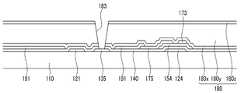
도 1은 본 발명의 한 실시예에 따른 액정 표시 장치를 도시한 배치도이다.
도 2는 도 1의 액정 표시 장치를 II-II 선을 따라 잘라 도시한 단면도이다.
도 3, 도 5, 도 7, 그리고 도 9는 본 발명의 한 실시예에 따른 액정 표시 장치의 제조 방법을 차례로 도시한 배치도이다.
도 4는 도 3의 액정 표시 장치의 박막 트랜지스터 표시판을 IV-IV 선을 따라 자른 단면도이다.
도 6은 도 5의 액정 표시 장치의 박막 트랜지스터 표시판을 VI-VI 선을 따라 자른 단면도이다.
도 8은 도 7의 액정 표시 장치의 박막 트랜지스터 표시판을 VIII-VIII 선을 따라 자른 단면도이다.
도 10은 도 9의 액정 표시 장치의 박막 트랜지스터 표시판을 X-X 선을 따라 자른 단면도이다.
도 11은 본 발명의 한 실시예에 따른 액정 표시 장치의 제조 방법을 도시한 단면도이다.
도 12는 본 발명의 한 실험예에 따른 액정 표시 장치의 박막 트랜지스터의 전압-전류를 나타내는 그래프이다.
도 13은 본 발명의 다른 한 실시예에 따른 액정 표시 장치의 배치도이다.
도 14는 도 13의 액정 표시 장치를 XIV-XIV 선을 따라 잘라 도시한 단면도이다.
도 15, 도 17, 그리고 도 19는 본 발명의 한 실시예에 따른 액정 표시 장치의 제조 방법을 차례로 도시한 배치도이다.
도 16은 도 15의 액정 표시 장치의 박막 트랜지스터 표시판을 XVI-XVI 선을 따라 자른 단면도이다.
도 18은 도 17의 액정 표시 장치의 박막 트랜지스터 표시판을 XVIII-XVIII 선을 따라 자른 단면도이다.
도 20은 도 19의 액정 표시 장치의 박막 트랜지스터 표시판을 XX-XX 선을 따라 자른 단면도이다.
도 21은 본 발명의 다른 한 실시예에 따른 액정 표시 장치의 제조 방법을 도시한 단면도이다.
도 22는 본 발명의 다른 한 실시예에 따른 액정 표시 장치의 배치도이다.
도 23은 도 22의 액정 표시 장치를 XXIII-XXIII 선을 따라 잘라 도시한 단면도이다.1 is a layout diagram showing a liquid crystal display device according to an embodiment of the present invention.
FIG. 2 is a cross-sectional view of the liquid crystal display device of FIG. 1 taken along line II-II.
3, 5, 7, and 9 are layout views sequentially illustrating a method of manufacturing a liquid crystal display according to an exemplary embodiment of the present invention.
4 is a cross-sectional view of the thin film transistor array panel of the liquid crystal display of FIG. 3 taken along line IV-IV.
6 is a cross-sectional view of the thin film transistor array panel of the liquid crystal display of FIG. 5 taken along the line VI-VI.
8 is a cross-sectional view of the thin film transistor array panel of the liquid crystal display of FIG. 7 taken along the line VIII-VIII.
FIG. 10 is a cross-sectional view taken along the line XX of the thin film transistor array panel of the liquid crystal display of FIG. 9.
11 is a cross-sectional view illustrating a method of manufacturing a liquid crystal display according to an exemplary embodiment of the present invention.
12 is a graph illustrating voltage-current of a thin film transistor of a liquid crystal display according to an exemplary embodiment of the present invention.
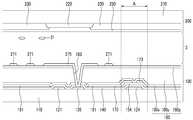
13 is a layout view of a liquid crystal display according to another exemplary embodiment of the present invention.
14 is a cross-sectional view of the liquid crystal display of FIG. 13 taken along the line XIV-XIV.
15, 17, and 19 are layout views sequentially illustrating a method of manufacturing a liquid crystal display according to an exemplary embodiment of the present invention.
FIG. 16 is a cross-sectional view of the thin film transistor array panel of the liquid crystal display of FIG. 15 taken along the line XVI-XVI.
FIG. 18 is a cross-sectional view of the thin film transistor array panel of the liquid crystal display of FIG. 17 taken along the line XVIII-XVIII.
20 is a cross-sectional view of the thin film transistor array panel of the liquid crystal display of FIG. 19 taken along the line XX-XX.
21 is a cross-sectional view illustrating a method of manufacturing a liquid crystal display device according to another exemplary embodiment of the present invention.
22 is a layout view of a liquid crystal display according to another exemplary embodiment of the present invention.
FIG. 23 is a cross-sectional view of the liquid crystal display of FIG. 22 taken along the line XXIII-XXIII.
그러면 첨부한 도면을 참고로 하여 본 발명의 실시예에 대하여 본 발명이 속하는 기술 분야에서 통상의 지식을 가진 자가 용이하게 실시할 수 있도록 상세히 설명한다. 그러나 본 발명은 여러 가지 상이한 형태로 구현될 수 있으며 여기에서 설명하는 실시예에 한정되지 않는다.DETAILED DESCRIPTION Hereinafter, exemplary embodiments of the present invention will be described in detail with reference to the accompanying drawings so that those skilled in the art may easily implement the present invention. The present invention may, however, be embodied in many different forms and should not be construed as limited to the embodiments set forth herein.
도면에서 여러 층 및 영역을 명확하게 표현하기 위하여 두께를 확대하여 나타내었다. 명세서 전체를 통하여 유사한 부분에 대해서는 동일한 도면 부호를 붙였다. 층, 막, 영역, 판 등의 부분이 다른 부분 "위에" 있다고 할 때, 이는 다른 부분 "바로 위에" 있는 경우 뿐만 아니라 그 중간에 또 다른 부분이 있는 경우도 포함한다. 반대로 어떤 부분이 다른 부분 "바로 위에" 있다고 할 때에는 중간에 다른 부분이 없는 것을 뜻한다.In the drawings, the thickness is enlarged to clearly represent the layers and regions. Like parts are designated with like reference numerals throughout the specification. Whenever a portion of a layer, film, region, plate, or the like is referred to as being "on" another portion, it includes not only the case where it is "directly on" another portion, but also the case where there is another portion in between. Conversely, when a part is "directly over" another part, it means that there is no other part in the middle.
그러면 도면을 참고로 하여 본 발명의 실시예에 따른 액정 표시 장치에 대하여 설명한다.A liquid crystal display according to an embodiment of the present invention will now be described with reference to the drawings.
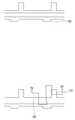
도 1은 본 발명의 한 실시예에 따른 액정 표시 장치를 도시한 배치도이고, 도 2는 도 1의 액정 표시 장치를 II-II 선을 따라 잘라 도시한 단면도이다.FIG. 1 is a layout view illustrating a liquid crystal display according to an exemplary embodiment of the present invention, and FIG. 2 is a cross-sectional view of the liquid crystal display of FIG. 1 taken along a line II-II.
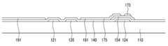
도 1 및 도 2를 참고하면, 본 발명의 한 실시예에 따른 액정 표시 장치는 서로 마주보는 하부 표시판(100) 및 상부 표시판(200)과 그 사이 주입되어 있는 액정층(3)을 포함한다.1 and 2, a liquid crystal display according to an exemplary embodiment includes a
먼저, 하부 표시판(100)에 대하여 설명한다.First, the
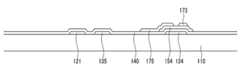
투명한 유리 또는 플라스틱 등으로 이루어진 제1 절연 기판(110) 위에 게이트선(121) 및 기준 전압선(131)을 포함하는 게이트 도전체가 형성되어 있다. 게이트선(121)은 게이트 전극(124) 및 다른 층 또는 외부 구동 회로와의 접속을 위한 게이트 패드부(도시하지 않음)를 포함한다.A gate conductor including a
게이트선(121)은 알루미늄(Al)이나 알루미늄 합금 등 알루미늄 계열 금속, 은(Ag)이나 은 합금 등 은계열 금속, 구리(Cu)나 구리 합금 등 구리 계열 금속, 몰리브덴(Mo)이나 몰리브덴 합금 등 몰리브덴 계열 금속, 크롬(Cr), 탄탈륨(Ta) 및 티타늄(Ti) 따위로 만들어질 수 있다. 그러나 게이트선(121)은 물리적 성질이 다른 적어도 두 개의 도전막을 포함하는 다중막 구조를 가질 수도 있다.The
기준 전압선(131)은 일정한 기준 전압을 전달하며, 뒤에서 설명할 기준 전극(270)과의 접속을 위한 확장부(135)를 포함한다. 기준 전압선(131)은 뒤에서 설명할 기준 전극(270)과 연결되어 기준 전극(270)에 기준 전압을 전달한다. 기준 전압선(131)은 게이트선(121)과 평행할 수 있으며, 게이트선(121)과 동일 물질로 이루어질 수 있다.The
게이트 도전체(121, 131) 위에는 질화규소(SiNx) 또는 산화규소(SiOx) 등으로 이루어지는 게이트 절연막(140)이 형성되어 있다. 게이트 절연막(140)은 물리적 성질이 다른 적어도 두 개의 절연층을 포함하는 다층막 구조를 가질 수도 있다.A
게이트 절연막(140) 위에는 금속 산화물 반도체, 예를 들어, IGZO(In-Ga-Zn-O) 등으로 만들어진 반도체(154)가 형성되어 있다. 반도체(154)는 게이트 전극(124)과 적어도 일부 중첩하고, 게이트 전극(124)보다 넓게 형성될 수 있다.A metal oxide semiconductor, for example, a
게이트 절연막(140) 및 반도체(154) 위에는 소스 전극(173)을 포함하는 데이터선(171)과 드레인 전극(175)을 포함하는 데이터 도전체가 형성되어 있다.A data conductor including a
데이터선(171)은 다른 층 또는 외부 구동 회로와의 접속을 위한 넓은 끝 부분(도시하지 않음)을 포함한다. 데이터선(171)은 데이터 신호를 전달하며 주로 세로 방향으로 뻗어 게이트선(121) 및 기준 전압선(131)과 교차한다. 데이터선(171)은 게이트선(121)과 함께 화소 영역을 형성한다. 이 때, 데이터선(171)은 액정 표시 장치의 최대 투과율을 얻기 위해서 굽어진 형상을 갖는 제1 굴곡부를 갖을 수 있으며, 굴곡부는 화소 영역의 중간 영역에서 서로 만나 V자 형태를 이룰 수 있다. 화소 영역의 중간 영역에는 제1 굴곡부와 소정의 각도를 이루도록 굽어진 제2 굴곡부를 더 포함할 수 있다.The
데이터선(171)의 제1 굴곡부는 설명할 배향막의 러빙 방향과 약 7°정도 이루도록 굽어 있을 수 있다. 화소 영역의 중간 영역에 배치되어 있는 제2 굴곡부는 제1 굴곡부와 약 7° 내지 약 15°정도 이루도록 더 굽어 있을 수 있다.The first bent portion of the
소스 전극(173)은 데이터선(171)의 일부이고, 데이터선(171)과 동일선 상에 배치된다. 드레인 전극(175)은 소스 전극(173)과 나란하게 뻗도록 형성되어 있다. 따라서, 드레인 전극(175)은 데이터선(171)의 일부와 나란하다. 또한 드레인 전극(175)의 확장부는 뒤에서 설명할 기준 전극(270)의 복수의 가지 전극(271)과 이격되어 형성되어 있으며, 드레인 전극(175)의 확장부의 가장 자리는 복수의 가지 전극(271)을 연결하는 가로 연결부(272)의 가장자리와 적어도 일부 평행할 수 있다. 드레인 전극(175)의 확장부를 복수의 가지 전극(271) 기준 전극(270)의 가지 전극(271)과 중첩하지 않도록 형성하여, 드레인 전극(175)이 전기장의 영향을 받는 액정층을 가리지 않아, 개구율 감소를 줄일 수 있다.The
게이트 전극(124), 소스 전극(173) 및 드레인 전극(175)은 반도체(154)와 함께 하나의 박막 트랜지스터(thin film transistor, TFT)를 이루며, 박막 트랜지스터의 채널(channel)은 소스 전극(173)과 드레인 전극(175) 사이의 반도체(154)에 형성된다.The
본 발명의 실시예에 따른 액정 표시 장치는 투명한 금속 산화물 반도체층으로 박막 트랜지스터의 채널을 형성하여, 게이트 전극(124)과 데이터 금속층으로 덮여 있지 않은 반도체층(154)는 빛을 투과할 수 있어, 액정 표시 장치의 개구율이 높아질 수 있다.The liquid crystal display according to the exemplary embodiment of the present invention forms a channel of the thin film transistor with a transparent metal oxide semiconductor layer, so that the
또한, 본 발명의 실시예에 따른 액정 표시 장치는 데이터선(171)과 동일선 상에 위치하는 소스 전극(173)과 데이터선(171)과 나란하게 뻗어 있는 드레인 전극(175)을 포함함으로써, 데이터 도전체가 차지하는 면적을 넓히지 않고도 박막 트랜지스터의 폭을 넓힐 수 있게 되고, 이에 따라 액정 표시 장치의 개구율이 증가할 수 있다.In addition, the liquid crystal display according to the exemplary embodiment of the present invention includes a
데이터선(171)과 드레인 전극(175)은 몰리브덴, 크롬, 탄탈륨 및 티타늄 등 내화성 금속(refractory metal)과 구리와 같은 저저항 도전체를 포함할 수 있다. 구체적으로, 데이터선(171)과 드레인 전극(175)은 티타늄과 구리를 포함할 수 있다.The
산화물 반도체를 포함하는 반도체층(154)과 데이터선(171) 및 드레인 전극 사이에는 산화물 반도체층과 데이터 금속층 사이의 반응이나 일부 성분의 확산을 방지하기 위한 배리어 층(barrier layer)을 더 포함할 수 있다. 예를 들어, 배리어 층은 아연갈륨산화물(GZO)을 포함할 수 있다.A barrier layer may be further included between the
드레인 전극(175)의 일부 및 게이트 절연막(140) 위에는 화소 전극(191)이 형성되어 있다.The
화소 전극(191)은 데이터선(171)의 제1 굴곡부 및 제2 굴곡부와 거의 나란한 한쌍의 굴곡변(curved edge)을 포함한다.The
화소 전극(191)은 드레인 전극(175)의 일부를 덮고 있어, 그 위에 배치되어 드레인 전극(175)과 물리적 전기적으로 직접 연결된다.The
화소 전극(191)은 다결정, 단결정 또는 비정질의 ITO(Indium tin oxide), 또는 IZO(Indium zinc oxide) 등의 투명한 도전 물질로 만들어질 수 있다.The
데이터 도전체(171, 175) 및 노출된 반도체(154), 그리고 화소 전극(191) 위에는 제1 보호막(180x)이 형성되어 있다. 제1 보호막(180x)은 유기 절연 물질 또는 무기 절연 물질 등으로 이루어질 수 있다. 도시하지는 않았지만, 제1 보호막(180x)은 하부막과 상부막을 포함할 수 있다. 데이터 도전체(171, 175)가 구리를 포함하는 경우, 제1 보호막(180x)의 하부막은 산화실리콘(SiOx)을 포함할 수 있고, 상부막은 질화실리콘(SiNx)을 포함할 수 있다.A
제1 보호막(180x) 위에는 제2 보호막(180y)이 형성되어 있다. 제2 보호막(180y)은 유기물질을 포함할 수 있다. 또한, 제2 보호막(180y)은 색필터일 수도 있다. 제2 보호막(180y)이 색필터인 경우, 제2 보호막(180y)은 기본색(primary color) 중 하나를 표시할 수 있다.The
제2 보호막(180y) 위에는 제3 보호막(180z)이 형성되어 있다. 제3 보호막(180z)은 유기 절연 물질 또는 무기 절연 물질 등으로 이루어질 수 있다. 제2 보호막(180y)이 색필터인 경우, 제3 보호막(180z)은 색필터의 물질이 확산되는 것을 방지할 수 있다. 만일 제2 보호막(180y)이 색필터가 아닌 경우, 제3 보호막(180z)은 생략 가능하다.The
보호막(180)에는 데이터선(171)의 끝 부분을 드러내는 접촉 구멍(contact hole)(도시하지 않음)이 형성되어 있고, 보호막(180) 및 게이트 절연막(140)에는 기준 전압선(131)의 확장부(135)를 드러내는 접촉 구멍(183) 및 게이트선(121)의 끝 부분을 드러내는 접촉 구멍(도시하지 않음)이 형성되어 있다.A passivation hole (not shown) is formed in the
보호막(180) 위에는 기준 전극(270)이 형성되어 있다. 기준 전극(270)은 화소 전극(191)과 중첩하며, 복수의 가지 전극(271)과 복수의 가지 전극(271)을 연결하는 가로 연결부(272) 및 가로 연결부(272)를 연결하는 세로 연결부(273)를 포함한다. 기준 전극(270)은 다결정, 단결정 또는 비정질의 ITO(indium tin oxide), 또는 IZO(indium zinc oxide) 등의 투명한 도전 물질로 만들어진다. 인접한 화소에 배치되어 있는 기준 전극(270)은 서로 연결되어 있다.The
기준 전극(270)의 가로 연결부(272)는 기준 전압선(131)의 확장부(135)를 향해 뻗은 기준 전극 확장부(275)를 가진다. 서로 이웃하는 화소에 배치되어 있는 기준 전극(270)은 서로 연결되어 있다.The
기준 전극(270)의 확장부(275)는 보호막(180) 및 게이트 절연막(140)에 형성되어 있는 접촉 구멍(183)을 통해 기준 전압선(131)과 물리적 전기적으로 연결된다.The
도시하지는 않았지만, 기준 전극(270) 및 보호막(180) 위에는 배향막(alignment layer)이 도포되어 있고, 배향막은 수평 배향막일 수 있으며, 일정한 방향으로 러빙되어 있다. 배향막의 러빙 방향은 기준 전극(270)의 가지 전극이 뻗어 있는 방향과 약 5° 내지 10°, 보다 구체적으로는 약 7° 정도 이룰 수 있다.Although not illustrated, an alignment layer is coated on the
본 실시예에 따른 액정 표시 장치의 화소 전극(191)은 드레인 전극(175)의 바로 위에서 드레인 전극(175)과 접촉하기 때문에, 제1 보호막(180x) 및 제2 보호막(180y)은 모두 화소 전극(191)과 기준 전극(270) 사이에 배치된다. 따라서, 제1 보호막(180x)과 제2 보호막(180y)은 하나의 마스크를 이용하여 패터닝될 수 있다. 또한, 제2 보호막(180y)이 색필터인 경우, 하프톤(half tone) 마스크를 이용하여, 원하는 위치에 배치되는 색필터, 제2 보호막(180y)을 형성함과 동시에, 제1 보호막(180x)에 접촉 구멍(183)을 형성할 수도 있다.Since the
화소 전극(191)은 드레인 전극(175)으로부터 데이터 전압을 인가 받고, 기준 전극(270)은 기준 전압선(131)으로부터 일정한 크기의 기준 전압을 인가 받는다. 기준 전극(270)은 서로 연결되어, 표시 영역 외부에 배치되어 있는 기준 전압 인가부로부터 기준 전압을 인가 받지만, 표시 영역 내에서 전압 강하 등을 방지하기 위하여, 기준 전압선(131)으로부터 같은 크기의 기준 전압을 인가 받는다.The
그러면, 상부 표시판(200)에 대하여 설명한다.The
투명한 유리 또는 플라스틱 등으로 만들어진 제2 절연 기판(210) 위에 차광 부재(light blocking member)(220)가 형성되어 있다. 차광 부재(220)는 블랙 매트릭스(black matrix)라고도 하며 빛샘을 막아준다.A
차광 부재(220)는 액정 표시 장치의 비 개구 영역에 형성되어 있다. 구체적으로, 불투명한 도전체로 이루어진 게이트 도전체와 데이터 도전체가 배치된 부분과, 박막 트랜지스터가 형성된 부분에 대응하는 위치에 형성될 수 있다. 그러나, 본 발명의 실시예에 따른 액정 표시 장치의 경우, 박막 트랜지스터의 채널을 금속 산화물 반도체층으로 이루어진 반도체(154)를 이용하기 때문에, 빛에 의한 박막 트랜지스터의 누설 전류 등이 없다. 따라서, 박막 트랜지스터에 대응하는 영역(A)에는 차광 부재(220)를 형성하지 않는다. 이에 의하여, 박막 트랜지스터의 채널을 형성하는 반도체(154) 중 불투명한 게이트 전극(124), 소스 전극(173) 및 드레인 전극(175)로 가려지지 않는 부분은 빛을 투과할 수 있다. 따라서, 액정 표시 장치의 개구율이 증가하게 된다.The
차광 부재(220) 및 제2 절연 기판(210) 위에는 색필터(230)가 형성되어 있다. 그러나, 하부 표시판(100)의 제2 보호막(180y)이 색필터인 경우, 색필터(230)는 생략된다. 차광 부재(220) 및 색필터(230) 위에는 덮개막(250)이 형성될 수 있다.The
액정층(3)은 양의 유전율 이방성을 가지는 네마틱(nematic) 액정 물질을 포함한다. 액정층(3)의 액정 분자는 그 장축 방향이 표시판(100, 200)에 평행하게 배열되어 있고, 그 방향이 하부 표시판(100)의 배향막의 러빙 방향으로부터 상부 표시판(200)에 이르기까지 나선상으로 90° 비틀린 구조를 가진다.The
데이터 전압이 인가된 화소 전극(191)은 기준 전압을 인가 받는 기준 전극(270)과 함께 전기장을 생성함으로써 두 전극(191, 270) 위에 위치하는 액정층(3)의 액정 분자는 전기장의 방향과 평행한 방향으로 회전한다. 이와 같이 결정된 액정 분자의 회전 방향에 따라 액정층을 통과하는 빛의 편광이 달라진다.The
기준 전극(271)과 화소 전극(191)의 가지 전극의 변 사이에 형성되는 전기장에 의해, 액정 표시 장치의 액정층(3)의 액정 분자(31)는 회전하게 된다. 이때, 본 발명의 실시예에 따른 액정 표시 장치는 액정층(3)의 액정 분자(31)가 소정 각도로 선경사되도록 배향막이 러빙되어 있고, 이 러빙 각도는 화소 전극(191)의 가지부와 약 7°를 이루기 때문에, 액정 분자(31)는 선경사된 방향으로 빨리 회전할 수 있게 된다.The
본 발명의 실시예에 따른 액정 표시 장치는 투명한 금속 산화물 반도체층으로 박막 트랜지스터의 채널을 형성하여, 게이트 전극(124)과 데이터 금속층으로 덮여 있지 않은 반도체층(154)는 빛을 투과할 수 있어, 액정 표시 장치의 개구율이 높아질 수 있다.The liquid crystal display according to the exemplary embodiment of the present invention forms a channel of the thin film transistor with a transparent metal oxide semiconductor layer, so that the
본 발명의 실시예에 따른 액정 표시 장치의 화소 전극(191)은 게이트 절연막(140)과 보호막(180) 사이에 배치되어 있고, 드레인 전극(175)의 일부를 덮어 직접 물리적, 전기적으로 연결되기 때문에, 화소 전극(191)과 드레인 전극(175)을 접촉 구멍을 통해 연결하는 기존의 액정 표시 장치에 비하여 개구율이 증가하게 된다.The
또한, 본 발명의 실시예에 따른 액정 표시 장치는 데이터선(171)과 동일선 상에 위치하는 소스 전극(173)과 데이터선(171)의 일부와 나란하게 뻗어 있는 드레인 전극(175)을 포함함으로써, 데이터 도전체가 차지하는 면적을 넓히지 않고도 박막 트랜지스터의 폭을 넓힐 수 있게 되고, 이에 따라 액정 표시 장치의 개구율이 증가할 수 있다.The liquid crystal display device according to the embodiment of the present invention includes the
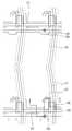
그러면, 도 1 및 도 2와 함께, 도 3 내지 도 11을 참고하여, 본 발명의 한 실시예에 따른 액정 표시 장치의 제조 방법을 설명한다.Next, a method of manufacturing a liquid crystal display according to an exemplary embodiment of the present invention will be described with reference to FIGS. 3 to 11 along with FIGS. 1 and 2.
도 3, 도 5, 도 7, 그리고 도 9는 본 발명의 한 실시예에 따른 액정 표시 장치의 박막 트랜지스터 표시판의 제조 방법을 차례로 도시한 배치도이고, 도 4는 도 3의 박막 트랜지스터 표시판의 IV-IV 선을 따라 자른 단면도이고, 도 6은 도 5의 박막 트랜지스터 표시판의 VI-VI 선을 따라 자른 단면도이고, 도 8은 도 7의 박막 트랜지스터 표시판의 VIII-VIII 선을 따라 자른 단면도이고, 도 10은 도 9의 박막 트랜지스터 표시판의 X-X 선을 따라 자른 단면도이고, 도 11은 본 발명의 한 실시예에 따른 액정 표시 장치의 제조 방법을 도시한 단면도이다.3, 5, 7, and 9 are layout views sequentially illustrating a method of manufacturing a thin film transistor array panel of a liquid crystal display according to an exemplary embodiment of the present invention, and FIG. 4 is IV- of the thin film transistor array panel of FIG. 3. 6 is a cross-sectional view taken along the line VI-VI of the thin film transistor array panel of FIG. 5, and FIG. 8 is a cross-sectional view taken along the line VIII-VIII of the thin film transistor array panel of FIG. 7, and FIG. 10. 9 is a cross-sectional view taken along line XX of the thin film transistor array panel of FIG. 9, and FIG. 11 is a cross-sectional view illustrating a method of manufacturing a liquid crystal display according to an exemplary embodiment of the present invention.
먼저, 도 3 및 도 4을 참고하면, 제1 절연 기판(110) 위에 게이트 전극(124)을 포함하는 게이트선(121) 및 기준 전압선(131)을 포함하는 게이트 도전체를 형성한다.First, referring to FIGS. 3 and 4, a gate conductor including a
게이트 도전체는 알루미늄(Al)이나 알루미늄 합금 등 알루미늄 계열 금속, 은(Ag)이나 은 합금 등 은계열 금속, 구리(Cu)나 구리 합금 등 구리 계열 금속, 몰리브덴(Mo)이나 몰리브덴 합금 등 몰리브덴 계열 금속, 크롬(Cr), 탄탈륨(Ta) 및 티타늄(Ti) 따위의 금속 층을 적층한 후, 사진 식각하여 형성한다.Gate conductors include aluminum-based metals such as aluminum (Al) and aluminum alloys, silver-based metals such as silver (Ag) and silver alloys, copper-based metals such as copper (Cu) and copper alloys, and molybdenum-based compounds such as molybdenum (Mo) and molybdenum alloys. Metal layers such as metal, chromium (Cr), tantalum (Ta) and titanium (Ti) are laminated and then formed by photolithography.
다음으로, 도 5 및 도 6을 참고하면, 게이트 도전체 위에 게이트 절연막(140)을 적층하고, 게이트 절연막(140) 위에 금속 산화물 반도체를 포함하는 반도체층(154), 그리고 소스 전극(173)을 포함하는 데이터선(171)과 드레인 전극(175)을 포함하는 데이터 도전체를 형성한다. 데이터선(171)은 액정 표시 장치의 최대 투과율을 얻기 위해서 굽어진 형상을 갖는 제1 굴곡부를 갖을 수 있으며, 굴곡부는 화소 영역의 중간 영역에서 서로 만나 V자 형태를 이룰 수 있다. 화소 영역의 중간 영역에는 제1 굴곡부와 소정의 각도를 이루도록 굽어진 제2 굴곡부를 더 포함할 수 있다.Next, referring to FIGS. 5 and 6, the
반도체층(154)은 금속 산화물 반도체를 포함함으로써, 빛에 의한 누설 전류 등이 발생하지 않아, 반도체층(154)에 대응하는 영역에는 도 2에 도시한 바와 같이, 차광 부재(220)가 배치되지 않을 수 있다.Since the
소스 전극(173)은 데이터선(171)과 동일선 상에 위치하고, 드레인 전극(175)은 데이터선(171)과 나란하게 뻗을 수 있다. 이에 의해, 데이터 도전체가 차지하는 면적을 넓히지 않고도 박막 트랜지스터의 폭을 넓힐 수 있게 되고, 이에 따라 액정 표시 장치의 개구율이 증가할 수 있다. 데이터선(171) 및 드레인 전극(175)은 몰리브덴, 크롬, 탄탈륨 및 티타늄 등 내화성 금속(refractory metal)과 구리와 같은 저저항 도전체를 포함할 수 있다. 구체적으로, 데이터선(171)과 드레인 전극(175)은 티타늄과 구리를 포함할 수 있다.The
도 7 및 도 8을 참고하면, 드레인 전극(175)의 일부 및 게이트 절연막(140) 위에 화소 전극(191)을 형성한다. 화소 전극(191)은 다결정, 단결정 또는 비정질의 ITO(Indium tin oxide), 또는 IZO(Indium zinc oxide) 등의 투명한 도전 물질을 적층하고 사진 식각하여 형성한다. 화소 전극(191)은 티타늄과 같은 내화성 금속과 구리를 포함하는 드레인 전극(175) 바로 위에 형성되어, 드레인 전극(175)과 직접 접촉하게 된다.7 and 8, the
그 후, 도 9 및 도 10을 참고하면, 데이터선(171) 및 드레인 전극(175), 화소 전극(191) 및 노출된 반도체(154) 부분 위에 보호막(180)을 형성한다. 보호막(180)은 유기 절연 물질 또는 무기 절연 물질 등으로 이루어진 제1 보호막(180x), 유기 물질을 포함하는 제2 보호막(180y)을 포함하고, 제2 보호막(180y)은 색필터일 수 있다. 제2 보호막(180y)이 색필터인 경우, 보호막(180)은 제3 보호막(180z)을 포함한다. 복수의 층을 포함하는 보호막(180)은 하나의 마스크를 이용하여 형성할 수 있고, 이 마스크는 하프톤 마스크일 수 있다.9 and 10, a
다음으로, 도 1 및 도 2에 도시한 바와 같이, 보호막(180) 위에 기준 전극(270)을 형성한다. 기준 전극(270)은 다결정, 단결정 또는 비정질의 ITO(indium tin oxide), 또는 IZO(indium zinc oxide) 등의 투명한 도전 물질로 만들어지고, 보호막(180) 및 게이트 절연막(140)에 형성되어 있는 접촉 구멍(183)을 통해 기준 전압선(131)과 물리적 전기적으로 연결된다. 이에 의해 하부 표시판(100)을 완성한다.Next, as shown in FIGS. 1 and 2, the
다음으로, 도 11에 도시한 바와 같이, 제2 절연 기판(210) 위에 게이트 도전체와 데이터 도전체에 대응하는 영역에 배치되어 있으며, 박막 트랜지스터에 대응하는 영역(A)에서는 제거되어 있는 차광 부재(220)를 형성하여 상부 표시판(200)을 완성한다.Next, as shown in FIG. 11, the light blocking member is disposed on the second insulating
그 후, 하부 표시판(100)과 상부 표시판(200)을 서로 마주보도록 정렬하여 부착하고, 액정층(3)을 주입한다. 또는 하부 표시판(100)과 상부 표시판(200) 중 어느 하나 위에 액정층(3)을 적하한 후, 두 표시판(100, 200)을 정렬시켜 부착할 수도 있다.Thereafter, the
그러면, 도 12를 참고하여, 본 발명의 한 실험예에 따른 액정 표시 장치의 박막 트랜지스터의 성능에 대하여 설명한다. 도 12는 본 발명의 한 실험예에 따른 액정 표시 장치의 박막 트랜지스터의 전압-전류를 나타내는 그래프이다.Next, the performance of the thin film transistor of the liquid crystal display according to the experimental example of the present invention will be described with reference to FIG. 12. 12 is a graph illustrating voltage-current of a thin film transistor of a liquid crystal display according to an exemplary embodiment of the present invention.
본 실험예에서는 박막 트랜지스터의 채널층을 금속 산화물 반도체로 형성한 후, 빛의 파장을 변화시키며, 박막 트랜지스터에 빛을 비춘 후, 전압-전류 특성을 측정하여, 그래프로 나타내었다.In the present experimental example, the channel layer of the thin film transistor was formed of a metal oxide semiconductor, the light wavelength was changed, the light was shined on the thin film transistor, and the voltage-current characteristics were measured.
도 12를 참고하면, 본 발명의 실시예에 따른 액정 표시 장치의 박막 트랜지스터와 같이, 채널 층을 금속 산화물 반도체로 형성한 경우, 시인 가능한 가시 광선의 파장 영역인 약 440nm 내지 680nm의 파장을 가진 빛을 투과하더라도 박막 트랜지스터의 전압-전류의 값이 변화하지 않음을 알 수 있었다.Referring to FIG. 12, when the channel layer is formed of a metal oxide semiconductor, such as a thin film transistor of a liquid crystal display according to an exemplary embodiment of the present invention, light having a wavelength of about 440 nm to 680 nm, which is a visible wavelength region of visible light It can be seen that the value of the voltage-current of the thin film transistor does not change even though the light is transmitted.
따라서, 본 발명의 실시예에 따른 액정 표시 장치와 같이, 금속 산화물 반도체로 박막 트랜지스터의 채널을 형성할 경우, 가시 광선 영역의 파장을 가지는 빛에 따라 누설 전류 등이 발생하지 않아, 박막 트랜지스터의 성능이 변화하지 않음을 알 수 있었다.Therefore, when the channel of the thin film transistor is formed of the metal oxide semiconductor as in the liquid crystal display according to the exemplary embodiment of the present invention, leakage current does not occur according to light having a wavelength in the visible light region, and thus the performance of the thin film transistor is improved. It was found that this did not change.
그러므로, 박막 트랜지스터에 대응하는 영역은 차광 부재(220)로 가리지 않아도, 박막 트랜지스터의 성능이 나빠지지 않으며, 투명한 금속 산화물 반도체를 통해 빛이 투과할 수 있어, 액정 표시 장치의 개구율을 높일 수 있음을 알 수 있었다.Therefore, even if the region corresponding to the thin film transistor is not covered by the
그러면, 도 13 및 도 14를 참고하여, 본 발명의 다른 한 실시예에 따른 액정 표시 장치에 대하여 설명한다.Next, a liquid crystal display according to another exemplary embodiment of the present invention will be described with reference to FIGS. 13 and 14.
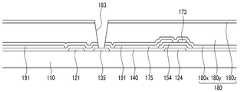
도 13 및 도 14를 참고하면, 본 실시예에 따른 액정 표시 장치는 도 1 및 도 2에 도시한 실시예에 따른 액정 표시 장치와 유사하다.13 and 14, the liquid crystal display according to the present exemplary embodiment is similar to the liquid crystal display according to the exemplary embodiment illustrated in FIGS. 1 and 2.
본 실시예에 따른 액정 표시 장치는 서로 마주보는 하부 표시판(100) 및 상부 표시판(200)과 그 사이 주입되어 있는 액정층(3)을 포함한다.The liquid crystal display according to the present exemplary embodiment includes a
하부 표시판(100)은 제1 절연 기판(110) 위에 형성되어 있는 게이트선(121) 및 기준 전압선(131)을 포함하는 게이트 도전체, 게이트 도전체(121, 131) 위에 형성되어 있는 게이트 절연막(140), 게이트 절연막(140) 위에 배치되어 있으며, 금속 산화물 반도체, 예를 들어, IGZO(In-Ga-Zn-O) 등으로 만들어진 반도체(154), 게이트 절연막(140)과 반도체(154) 위에 형성되어 있는 데이터 도전체(171, 175) 및 화소 전극(191), 데이터 도전체(171, 175) 및 노출된 반도체(154), 그리고 화소 전극(191) 위에 형성되어 있는 보호막(180), 보호막(180) 위에 형성되어 있으며, 접촉 구멍(183)을 통해 기준 전압선(131)의 확장부(135)와 연결되어 있는 기준 전극(270)을 포함한다.The
상부 표시판(200)은 제2 절연 기판(210) 위에 형성되어 있는 차광 부재(220)를 포함하는데, 박막 트랜지스터에 대응하는 영역(A)에는 차광 부재(220)를 형성하지 않는다. 이에 의하여, 박막 트랜지스터의 채널을 형성하는 반도체(154) 중 불투명한 게이트 전극(124), 소스 전극(173) 및 드레인 전극(175)로 가려지지 않는 부분은 빛을 투과할 수 있다. 따라서, 액정 표시 장치의 개구율이 증가하게 된다. 차광 부재(220) 및 제2 절연 기판(210) 위에는 색필터(230)가 형성되어 있다. 그러나, 하부 표시판(100)의 제2 보호막(180y)이 색필터인 경우, 색필터(230)는 생략될 수 있다. 차광 부재(220) 및 색필터(230) 위에는 덮개막(250)이 형성될 수 있다.The
그러나, 본 실시예에 따른 액정 표시 장치는 도 1 및 도 2에 도시한 실시예에 따른 액정 표시 장치와는 달리, 본 실시예에 따른 액정 표시 장치의 데이터 도전체(171, 175)는 화소 전극(191)과 동일한 층으로 이루어진다. 즉, 데이터 도전체(171, 175)와 화소 전극(191)은 동일한 층으로 동시에 형성되며, 투명한 금속층으로 이루어질 수 있다. 이에 의하여, 액정 표시 장치의 제조 단계가 더 간단해 지고, 액정 표시 장치의 개구율은 더욱 증가하게 된다.However, unlike the liquid crystal display according to the exemplary embodiment illustrated in FIGS. 1 and 2, the liquid crystal display according to the present exemplary embodiment may include the pixel electrodes of the
본 발명의 실시예에 따른 액정 표시 장치는 투명한 금속 산화물 반도체층으로 박막 트랜지스터의 채널을 형성하여, 게이트 전극(124)과 데이터 금속층으로 덮여 있지 않은 반도체층(154)는 빛을 투과할 수 있어, 액정 표시 장치의 개구율이 높아질 수 있다.The liquid crystal display according to the exemplary embodiment of the present invention forms a channel of the thin film transistor with a transparent metal oxide semiconductor layer, so that the
본 발명의 실시예에 따른 액정 표시 장치의 화소 전극(191)은 게이트 절연막(140)과 보호막(180) 사이에 배치되어 있고, 드레인 전극(175)의 일부를 덮어 직접 물리적 전기적으로 연결되기 때문에, 화소 전극(191)과 드레인 전극(175)을 접촉 구멍을 통해 연결하는 기존의 액정 표시 장치에 비하여 개구율이 증가하게 된다.Since the
또한, 본 발명의 실시예에 따른 액정 표시 장치는 데이터선(171)과 동일선 상에 위치하는 소스 전극(173)과 데이터선(171)의 일부와 나란하게 뻗어 있는 드레인 전극(175)을 포함함으로써, 데이터 도전체가 차지하는 면적을 넓히지 않고도 박막 트랜지스터의 폭을 넓힐 수 있게 되고, 이에 따라 액정 표시 장치의 개구율이 증가할 수 있다.The liquid crystal display device according to the embodiment of the present invention includes the
또한, 본 발명의 실시예에 따른 액정 표시 장치는 데이터 도전체(171 175)와 화소 전극(191)을 동일한 층으로 형성하여, 투명한 금속층으로 형성할 수 있다. 이에 의하여, 액정 표시 장치의 제조 단계가 더 간단해 지고, 액정 표시 장치의 개구율은 더욱 증가하게 된다.In addition, in the liquid crystal display according to the exemplary embodiment of the present invention, the
그러면, 도 13 및 도 14와 함께, 도 15 내지 도 21을 참고하여, 본 발명의 다른 한 실시예에 따른 액정 표시 장치의 제조 방법을 설명한다.Next, a method of manufacturing a liquid crystal display according to another exemplary embodiment of the present invention will be described with reference to FIGS. 15 to 21 along with FIGS. 13 and 14.
도 15, 도 17, 그리고 도 19는 본 발명의 다른 한 실시예에 따른 액정 표시 장치의 박막 트랜지스터 표시판의 제조 방법을 차례로 도시한 배치도이고, 도 16은 도 15의 박막 트랜지스터 표시판의 XVI-XVI 선을 따라 자른 단면도이고, 도 18은 도 17의 박막 트랜지스터 표시판의 XVIII-XVIII 선을 따라 자른 단면도이고, 도 20은 도 19의 박막 트랜지스터 표시판의 XX-XX 선을 따라 자른 단면도이고, 도 21은 본 발명의 한 실시예에 따른 액정 표시 장치의 제조 방법을 도시한 단면도이다.15, 17, and 19 are layout views sequentially illustrating a method of manufacturing a thin film transistor array panel of a liquid crystal display according to another exemplary embodiment, and FIG. 16 is an XVI-XVI line of the thin film transistor array panel of FIG. 15. 18 is a cross-sectional view taken along the line XVIII-XVIII of the thin film transistor array panel of FIG. 17, FIG. 20 is a cross-sectional view taken along the line XX-XX of the thin film transistor array panel of FIG. 19, and FIG. A cross-sectional view illustrating a method of manufacturing a liquid crystal display device according to an exemplary embodiment of the present invention.
도 15 및 도 16을 참고하면, 제1 절연 기판(110) 위에 게이트 전극(124)을 포함하는 게이트선(121) 및 기준 전압선(131)을 포함하는 게이트 도전체를 형성한다.15 and 16, a gate conductor including a
도 17 및 도 18을 참고하면, 게이트 도전체 위에 게이트 절연막(140)을 적층하고, 게이트 절연막(140) 위에 금속 산화물 반도체를 포함하는 반도체층(154), 그리고 소스 전극(173)을 포함하는 데이터선(171)과 드레인 전극(175)을 포함하는 데이터 도전체와 동일한 층으로 이루어진 화소 전극(191)을 형성한다. 데이터 도전체(171, 175)와 화소 전극(191)은 다결정, 단결정 또는 비정질의 ITO(Indium tin oxide), 또는 IZO(Indium zinc oxide) 등의 투명한 도전 물질을 적층하고 사진 식각하여 형성한다.17 and 18, data including a
도 19 및 도 20을 참고하면, 데이터선(171) 및 드레인 전극(175), 화소 전극(191) 및 노출된 반도체(154) 부분 위에 보호막(180)을 형성한다. 보호막(180)은 보호막(180)은 유기 절연 물질 또는 무기 절연 물질 등으로 이루어진 제1 보호막(180x), 유기 물질을 포함하는 제2 보호막(180y)을 포함하고, 제2 보호막(180y)은 색필터일 수 있다. 제2 보호막(180y)이 색필터인 경우, 보호막(180)은 제3 보호막(180z)을 포함한다. 복수의 층을 포함하는 보호막(180)은 하나의 마스크를 이용하여 형성할 수 있고, 이 마스크는 하프톤 마스크일 수 있다.19 and 20, the
그 후, 도 13 및 도 14에 도시한 바와 같이, 보호막(180) 위에 기준 전극(270)을 형성한다. 이에 의해 하부 표시판(100)을 완성한다.Thereafter, as shown in FIGS. 13 and 14, the
그 후, 도 21에 도시한 바와 같이, 제2 절연 기판(210) 위에 게이트 도전체와 데이터 도전체에 대응하는 영역에 배치되어 있으며, 박막 트랜지스터에 대응하는 영역(A)에서는 제거되어 있는 차광 부재(220)를 형성하여 상부 표시판(200)을 완성한다.After that, as shown in FIG. 21, the light blocking member is disposed on the second insulating
그 후, 하부 표시판(100)과 상부 표시판(200)을 서로 마주보도록 정렬하여 부착하고, 액정층(3)을 주입한다. 또는 하부 표시판(100)과 상부 표시판(200) 중 어느 하나 위에 액정층(3)을 적하한 후, 두 표시판(100, 200)을 정렬시켜 부착할 수도 있다.Thereafter, the
그러면, 도 22 및 도 23을 참고하여, 본 발명의 다른 한 실시예에 따른 액정 표시 장치에 대하여 설명한다.Next, a liquid crystal display according to another exemplary embodiment of the present invention will be described with reference to FIGS. 22 and 23.
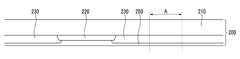
도 22 및 도 23을 참고하면, 본 실시예에 따른 액정 표시 장치는 서로 마주하는 하부 표시판(100)과 상부 표시판(200), 그리고 이들 두 표시판(100, 200) 사이에 들어 있는 액정층(3)을 포함한다.Referring to FIGS. 22 and 23, the liquid crystal display according to the present exemplary embodiment includes a
먼저 박막 트랜지스터 표시판(100)에 대하여 설명한다.First, the thin film
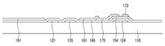
제1 절연 기판(110) 위에 게이트선(121) 및 기준 전압선(131)을 포함하는 복수의 게이트 도전체가 형성되어 있다.A plurality of gate conductors including the
게이트선(121)은 게이트 신호를 전달하며 주로 가로 방향으로 뻗어 있다. 각 게이트선(121)은 아래로 돌출한 복수의 게이트 전극(gate electrode)(124)을 포함한다.The
기준 전압선(131)은 소정의 전압을 인가 받으며, 게이트선(121)과 거의 나란하게 뻗은 줄기선과 이로부터 갈라진 복수 쌍의 제1 및 제2 유지 전극(133a, 133b)을 포함한다.The
게이트선(121) 및 기준 전압선(131) 위에는 게이트 절연막(140)이 형성되어 있다.The
게이트 절연막(140) 위에는 반도체(151, 154)가 형성되어 있다. 반도체(151, 154)는 주로 세로 방향으로 뻗어 있으며, 게이트 전극(124)을 향하여 뻗어 나온 돌출부(154)를 포함한다.
반도체(151, 154)는 금속 산화물 반도체를 포함한다.The
게이트 절연막(140) 및 반도체(151, 154) 위에는 소스 전극(173)을 포함하는 데이터선(171)과 드레인 전극(175)이 형성되어 있다.The
하나의 게이트 전극(124), 하나의 소스 전극(173) 및 하나의 드레인 전극(175)은 반도체(154)와 함께 하나의 박막 트랜지스터(thin film transistor, TFT)를 이루며, 박막 트랜지스터의 채널(channel)은 소스 전극(173)과 드레인 전극(175) 사이의 반도체(154)에 형성된다. 반도체(154)는 금속 산화물 반도체층을 포함한다.One
데이터선(171), 드레인 전극(175) 및 노출된 반도체(154) 부분 위에는 보호막 (180)이 형성되어 있다.The
보호막(180)에는 드레인 전극(175)을 드러내는 제1 접촉 구멍(185)이 형성되어 있다. 보호막(180) 위에는 화소 전극(191)이 형성되어 있다. 화소 전극(191)은 ITO 또는 IZO 등의 투명한 도전 물질로 만들어질 수 있다. 화소 전극(191)은 제1 접촉 구멍(185)을 통하여 드레인 전극(175)과 물리적ㅇ전기적으로 연결되어 있으며, 드레인 전극(175)으로부터 데이터 전압을 인가 받는다.The
다음으로, 상부 표시판(200)에 대하여 설명한다.Next, the
제2 절연 기판(210) 위에는 차광 부재(220)가 형성되어 있다. 본 발명의 실시예에 따른 액정 표시 장치의 박막 트랜지스터의 채널을 금속 산화물 반도체층으로 이루어진 반도체(154)를 이용하기 때문에, 빛에 의한 박막 트랜지스터의 누설 전류 등이 없다. 따라서, 박막 트랜지스터에 대응하는 영역(A)에는 차광 부재(220)를 형성하지 않는다. 이에 의하여, 박막 트랜지스터의 채널을 형성하는 반도체(154) 중 불투명한 게이트 전극(124), 소스 전극(173) 및 드레인 전극(175)로 가려지지 않는 부분은 빛을 투과할 수 있다. 따라서, 액정 표시 장치의 개구율이 증가하게 된다.The
제2 절연 기판(210) 및 차광 부재(220)의 일부 위에는 복수의 색필터(230)가 형성되어 있다. 색필터(230)는 차광 부재(220)로 둘러싸인 영역 내에 대부분 존재한다.A plurality of
색필터(230) 위에는 색필터(230)를 평탄화하기 위한 덮개막(overcoat)(250)이 형성되어 있다. 덮개막(250)은 폴리이미드(polyimide) 따위의 절연 물질로 만들어질 수 있으며, 색필터(230)가 노출되는 것을 방지하고 평탄면을 제공한다.An
덮개막(250) 위에는 공통 전극(270)이 형성되어 있다. 공통 전극(270)은 ITO 또는 IZO 따위의 투명한 도전체 따위로 만들어진다.A
액정층(3)은 양의 유전율 이방성을 가지는 네마틱(nematic) 액정 물질을 포함한다. 액정층(3)의 액정 분자는 그 장축 방향이 표시판(100, 200)에 평행하게 배열되어 있고, 그 방향이 하부 표시판(100)의 배향막의 러빙 방향으로부터 상부 표시판(200)에 이르기까지 나선상으로 90° 비틀린 구조를 가진다.The
데이터 전압이 인가된 화소 전극(191)은 공통 전극(270)과 함께 전기장을 생성함으로써 두 전극(191, 270) 위에 위치하는 액정층(3)의 액정 분자는 전기장의 방향과 평행한 방향으로 회전한다. 이와 같이 결정된 액정 분자의 회전 방향에 따라 액정층을 통과하는 빛의 편광이 달라진다.Since the
본 발명의 실시예에 따른 액정 표시 장치는 투명한 금속 산화물 반도체층으로 박막 트랜지스터의 채널을 형성하여, 게이트 전극(124)과 데이터 금속층으로 덮여 있지 않은 반도체층(154)는 빛을 투과할 수 있어, 액정 표시 장치의 개구율이 높아질 수 있다.The liquid crystal display according to the exemplary embodiment of the present invention forms a channel of the thin film transistor with a transparent metal oxide semiconductor layer, so that the
이상에서 본 발명의 바람직한 실시예들에 대하여 상세하게 설명하였지만 본 발명의 권리범위는 이에 한정되는 것은 아니고 다음의 청구범위에서 정의하고 있는 본 발명의 기본 개념을 이용한 당업자의 여러 변형 및 개량 형태 또한 본 발명의 권리범위에 속하는 것이다.While the present invention has been particularly shown and described with reference to exemplary embodiments thereof, it is to be understood that the invention is not limited to the disclosed exemplary embodiments, And falls within the scope of the invention.
Claims (30)
Translated fromKorean상기 제1 기판 위에 형성되어 있는 게이트 전극,
상기 게이트 전극 위에 형성되어 있는 게이트 절연막,
상기 게이트 절연막 위에 형성되어 있는 반도체,
상기 반도체 위에 형성되어 있는 소스 전극 및 드레인 전극,
상기 제1 기판과 마주하는 제2 기판,
상기 제2 기판 위에 형성되어 있는 차광 부재를 포함하고,
상기 반도체는 금속 산화물 반도체를 포함하고,
상기 차광 부재는 상기 반도체 중 적어도 일부에 대응하는 영역에는 형성되지 않는 액정 표시 장치.
First substrate,
A gate electrode formed on the first substrate,
A gate insulating film formed on the gate electrode,
A semiconductor formed on the gate insulating film,
A source electrode and a drain electrode formed on the semiconductor,
A second substrate facing the first substrate,
A light blocking member formed on the second substrate,
The semiconductor comprises a metal oxide semiconductor,
The light blocking member is not formed in a region corresponding to at least part of the semiconductor.
상기 게이트 전극의 폭은 상기 반도체의 폭보다 좁고,
상기 소스 전극과 상기 드레인 전극은 평행하게 뻗은 액정 표시 장치.
In claim 1,
The width of the gate electrode is narrower than the width of the semiconductor,
The liquid crystal display device of which the source electrode and the drain electrode extend in parallel.
상기 드레인 전극의 일부분 바로 위에 형성되어 있는 화소 전극을 더 포함하는 액정 표시 장치.
3. The method of claim 2,
And a pixel electrode formed directly on a portion of the drain electrode.
상기 화소 전극 위에 형성되어 있는 보호막,
상기 보호막 위에 형성되어 있는 기준 전극을 더 포함하는 액정 표시 장치.
4. The method of claim 3,
A protective film formed on the pixel electrode,
And a reference electrode formed on the passivation layer.
상기 보호막은 색필터를 포함하는 액정 표시 장치.
5. The method of claim 4,
The protective film includes a color filter.
상기 제2 기판 위에 배치되어 있는 공통 전극을 더 포함하는 액정 표시 장치.
4. The method of claim 3,
And a common electrode disposed on the second substrate.
상기 제2 기판 위에 배치되어 있는 색필터를 더 포함하는 액정 표시 장치.
The method of claim 6,
And a color filter disposed on the second substrate.
상기 드레인 전극과 동일한 층으로 이루어진 화소 전극을 더 포함하는 액정 표시 장치.
3. The method of claim 2,
And a pixel electrode formed of the same layer as the drain electrode.
상기 화소 전극 위에 형성되어 있는 보호막,
상기 보호막 위에 형성되어 있는 기준 전극을 더 포함하는 액정 표시 장치.
9. The method of claim 8,
A protective film formed on the pixel electrode,
And a reference electrode formed on the passivation layer.
상기 보호막은 색필터를 포함하는 액정 표시 장치.
The method of claim 9,
The protective film includes a color filter.
상기 제2 기판 위에 배치되어 있는 공통 전극을 더 포함하는 액정 표시 장치.
9. The method of claim 8,
And a common electrode disposed on the second substrate.
상기 제2 기판 위에 배치되어 있는 색필터를 더 포함하는 액정 표시 장치.
12. The method of claim 11,
And a color filter disposed on the second substrate.
상기 드레인 전극의 일부분 바로 위에 형성되어 있는 화소 전극을 더 포함하는 액정 표시 장치.
In claim 1,
And a pixel electrode formed directly on a portion of the drain electrode.
상기 화소 전극 위에 형성되어 있는 보호막,
상기 보호막 위에 형성되어 있는 기준 전극을 더 포함하는 액정 표시 장치.
In claim 13,
A protective film formed on the pixel electrode,
And a reference electrode formed on the passivation layer.
상기 보호막은 색필터를 포함하는 액정 표시 장치.
The method of claim 14,
The protective film includes a color filter.
상기 제2 기판 위에 배치되어 있는 공통 전극을 더 포함하는 액정 표시 장치.
In claim 13,
And a common electrode disposed on the second substrate.
상기 제2 기판 위에 배치되어 있는 색필터를 더 포함하는 액정 표시 장치.
17. The method of claim 16,
And a color filter disposed on the second substrate.
상기 드레인 전극과 동일한 층으로 이루어진 화소 전극을 더 포함하는 액정 표시 장치.
In claim 1,
And a pixel electrode formed of the same layer as the drain electrode.
상기 화소 전극 위에 형성되어 있는 보호막,
상기 보호막 위에 형성되어 있는 기준 전극을 더 포함하는 액정 표시 장치.
The method of claim 18,
A protective film formed on the pixel electrode,
And a reference electrode formed on the passivation layer.
상기 보호막은 색필터를 포함하는 액정 표시 장치.
20. The method of claim 19,
The protective film includes a color filter.
상기 제2 기판 위에 배치되어 있는 공통 전극을 더 포함하는 액정 표시 장치.
The method of claim 18,
And a common electrode disposed on the second substrate.
상기 제2 기판 위에 배치되어 있는 색필터를 더 포함하는 액정 표시 장치.
22. The method of claim 21,
And a color filter disposed on the second substrate.
상기 게이트 전극 위에 게이트 절연막을 형성하는 단계
상기 게이트 절연막 위에 금속 산화물 반도체를 포함하는 반도체를 형성하는 단계,
상기 반도체 위에 소스 전극 및 드레인 전극을 형성하는 단계,
상기 제1 기판과 마주하는 제2 기판 위에 차광 부재를 형성하는 단계를 포함하고,
상기 차광 부재는 상기 반도체 중 적어도 일부에 대응하는 영역에는 형성하지 않는 액정 표시 장치의 제조 방법.
Forming a gate electrode on the first substrate,
Forming a gate insulating film on the gate electrode
Forming a semiconductor including a metal oxide semiconductor on the gate insulating film,
Forming a source electrode and a drain electrode on the semiconductor,
Forming a light blocking member on a second substrate facing the first substrate,
The light blocking member is not formed in a region corresponding to at least part of the semiconductor.
상기 게이트 전극의 폭은 상기 반도체의 폭보다 좁게 형성하는 액정 표시 장치의 제조 방법.
24. The method of claim 23,
The width of the gate electrode is formed smaller than the width of the semiconductor manufacturing method of the liquid crystal display device.
상기 드레인 전극의 일부분 바로 위에 화소 전극을 형성하는 단계를 더 포함하는 액정 표시 장치의 제조 방법.
24. The method of claim 23,
And forming a pixel electrode directly over a portion of the drain electrode.
상기 화소 전극 위에 보호막을 형성하는 단계, 그리고
상기 보호막 위에 기준 전극을 형성하는 단계를 더 포함하는 액정 표시 장치의 제조 방법.
26. The method of claim 25,
Forming a protective film on the pixel electrode, and
And forming a reference electrode on the passivation layer.
상기 보호막을 형성하는 단계는 색필터를 형성하는 단계를 포함하는 액정 표시 장치의 제조 방법.
The method of claim 26,
The forming of the passivation layer may include forming a color filter.
상기 제2 기판 위에 공통 전극을 형성하는 단계를 더 포함하는 액정 표시 장치의 제조 방법.
26. The method of claim 25,
And forming a common electrode on the second substrate.
상기 제2 기판 위에 색필터를 형성하는 단계를 더 포함하는 액정 표시 장치의 제조 방법.
29. The method of claim 28,
And forming a color filter on the second substrate.
상기 드레인 전극을 형성하는 단계에서, 상기 드레인 전극과 동일한 층으로 이루어진 화소 전극을 함께 형성하는 액정 표시 장치의 제조 방법.24. The method of claim 23,
And forming a pixel electrode formed of the same layer as the drain electrode in the forming of the drain electrode.
Priority Applications (2)
| Application Number | Priority Date | Filing Date | Title |
|---|---|---|---|
| KR1020120006980AKR20130085859A (en) | 2012-01-20 | 2012-01-20 | Liguif crystal display and manufacturing method thereof |
| US13/551,417US8767150B2 (en) | 2012-01-20 | 2012-07-17 | Liquid crystal display and method of manufacturing the same |
Applications Claiming Priority (1)
| Application Number | Priority Date | Filing Date | Title |
|---|---|---|---|
| KR1020120006980AKR20130085859A (en) | 2012-01-20 | 2012-01-20 | Liguif crystal display and manufacturing method thereof |
Publications (1)
| Publication Number | Publication Date |
|---|---|
| KR20130085859Atrue KR20130085859A (en) | 2013-07-30 |
Family
ID=48796939
Family Applications (1)
| Application Number | Title | Priority Date | Filing Date |
|---|---|---|---|
| KR1020120006980ACeasedKR20130085859A (en) | 2012-01-20 | 2012-01-20 | Liguif crystal display and manufacturing method thereof |
Country Status (2)
| Country | Link |
|---|---|
| US (1) | US8767150B2 (en) |
| KR (1) | KR20130085859A (en) |
Families Citing this family (5)
| Publication number | Priority date | Publication date | Assignee | Title |
|---|---|---|---|---|
| US9417475B2 (en)* | 2013-02-22 | 2016-08-16 | Semiconductor Energy Laboratory Co., Ltd. | Display device |
| KR20150024646A (en)* | 2013-08-27 | 2015-03-09 | 삼성디스플레이 주식회사 | Liquid crystal display |
| KR20150107965A (en)* | 2014-03-14 | 2015-09-24 | 삼성디스플레이 주식회사 | Liquid crystal display device and methdo for manufacturing the same |
| KR102240291B1 (en)* | 2014-11-26 | 2021-04-14 | 삼성디스플레이 주식회사 | Liquid crystal display |
| KR102636515B1 (en) | 2017-01-06 | 2024-02-15 | 삼성디스플레이 주식회사 | Organic light emitting display apparatus |
Citations (3)
| Publication number | Priority date | Publication date | Assignee | Title |
|---|---|---|---|---|
| KR20100027419A (en)* | 2008-09-02 | 2010-03-11 | 삼성전자주식회사 | Liquid crystal display |
| KR20100061366A (en)* | 2008-11-28 | 2010-06-07 | 가부시키가이샤 한도오따이 에네루기 켄큐쇼 | A liquid crystal display device |
| KR20100090641A (en)* | 2009-02-06 | 2010-08-16 | 가부시키가이샤 한도오따이 에네루기 켄큐쇼 | Semiconductor device and method of manufacturing the semiconductor device |
Family Cites Families (12)
| Publication number | Priority date | Publication date | Assignee | Title |
|---|---|---|---|---|
| KR100653466B1 (en) | 1997-12-08 | 2007-02-05 | 비오이 하이디스 테크놀로지 주식회사 | Manufacturing method of liquid crystal display device |
| KR20080062647A (en) | 2006-12-29 | 2008-07-03 | 엘지디스플레이 주식회사 | Thin film transistor array substrate and its manufacturing method |
| CN101325631B (en) | 2007-06-14 | 2010-10-20 | 华为技术有限公司 | Method and device for estimating pitch period |
| KR101396809B1 (en) | 2007-07-11 | 2014-05-19 | 엘지디스플레이 주식회사 | An Array Substrate of Liquid Crystal Display Device and the method for fabricating thereof |
| EP2183780A4 (en) | 2007-08-02 | 2010-07-28 | Applied Materials Inc | THIN FILM TRANSISTORS USING THIN FILM SEMICONDUCTOR MATERIALS |
| KR101435501B1 (en) | 2008-10-03 | 2014-08-29 | 가부시키가이샤 한도오따이 에네루기 켄큐쇼 | Display device |
| KR20160072845A (en) | 2008-10-24 | 2016-06-23 | 가부시키가이샤 한도오따이 에네루기 켄큐쇼 | Semiconductor device and method for manufacturing the same |
| EP2184783B1 (en) | 2008-11-07 | 2012-10-03 | Semiconductor Energy Laboratory Co, Ltd. | Semiconductor device and method for manufacturing the same |
| TWI487104B (en) | 2008-11-07 | 2015-06-01 | Semiconductor Energy Lab | Semiconductor device and method of manufacturing same |
| KR101518851B1 (en) | 2009-05-15 | 2015-05-12 | 엘지디스플레이 주식회사 | Method of fabricating array substrate |
| KR101644321B1 (en) | 2009-12-20 | 2016-08-01 | 엘지디스플레이 주식회사 | TFT array substrate using a oxidized semiconductor and Method of fabricating the same |
| US20120001179A1 (en)* | 2010-07-02 | 2012-01-05 | Semiconductor Energy Laboratory Co., Ltd. | Semiconductor device |
- 2012
- 2012-01-20KRKR1020120006980Apatent/KR20130085859A/ennot_activeCeased
- 2012-07-17USUS13/551,417patent/US8767150B2/enactiveActive
Patent Citations (3)
| Publication number | Priority date | Publication date | Assignee | Title |
|---|---|---|---|---|
| KR20100027419A (en)* | 2008-09-02 | 2010-03-11 | 삼성전자주식회사 | Liquid crystal display |
| KR20100061366A (en)* | 2008-11-28 | 2010-06-07 | 가부시키가이샤 한도오따이 에네루기 켄큐쇼 | A liquid crystal display device |
| KR20100090641A (en)* | 2009-02-06 | 2010-08-16 | 가부시키가이샤 한도오따이 에네루기 켄큐쇼 | Semiconductor device and method of manufacturing the semiconductor device |
Also Published As
| Publication number | Publication date |
|---|---|
| US20130188116A1 (en) | 2013-07-25 |
| US8767150B2 (en) | 2014-07-01 |
Similar Documents
| Publication | Publication Date | Title |
|---|---|---|
| JP5351388B2 (en) | Display device | |
| KR101492106B1 (en) | Liquid crystal display device and manufacturing method thereof | |
| CN103915448B (en) | Thin-film transistor display panel | |
| KR101252001B1 (en) | Liquid crystal display and method of manufacturing thereof | |
| KR20140029021A (en) | Liquid crystal display | |
| KR102074424B1 (en) | Liquid crystal display and manufacturing method thereof | |
| KR20080067406A (en) | Thin film transistor array panel | |
| JP6676416B2 (en) | Liquid crystal display | |
| KR102040084B1 (en) | Display device | |
| KR101981593B1 (en) | Liquid crystal display and manufacturing method thereof | |
| KR20160125598A (en) | Thin film transistor array substrate and method of manufacturing thereof and display device having the thin film transistor array substrate | |
| KR20160110671A (en) | Liquid crystal display device | |
| KR20130085859A (en) | Liguif crystal display and manufacturing method thereof | |
| CN105842945B (en) | LCD Monitor | |
| JP2006058894A (en) | Liquid crystal display | |
| KR20170052730A (en) | Liquid crystal display device | |
| US10895786B2 (en) | Liquid crystal display device and method of manufacturing the same | |
| US9595542B2 (en) | Thin film transistor array panel and manufacturing method thereof | |
| KR20150109544A (en) | Display device and manufacturing method thereof | |
| KR102365290B1 (en) | Display device and method of manufacturing the same | |
| KR102190766B1 (en) | Liquid crystal display | |
| KR102050512B1 (en) | Liquid crystal display | |
| KR102295478B1 (en) | Liquid crystal display | |
| KR102087197B1 (en) | Liquid crystal display and manufacturing method thereof | |
| KR102233865B1 (en) | Liquid crystal display |
Legal Events
| Date | Code | Title | Description |
|---|---|---|---|
| PA0109 | Patent application | Patent event code:PA01091R01D Comment text:Patent Application Patent event date:20120120 | |
| N231 | Notification of change of applicant | ||
| PN2301 | Change of applicant | Patent event date:20120913 Comment text:Notification of Change of Applicant Patent event code:PN23011R01D | |
| PG1501 | Laying open of application | ||
| PA0201 | Request for examination | Patent event code:PA02012R01D Patent event date:20170113 Comment text:Request for Examination of Application Patent event code:PA02011R01I Patent event date:20120120 Comment text:Patent Application | |
| E902 | Notification of reason for refusal | ||
| PE0902 | Notice of grounds for rejection | Comment text:Notification of reason for refusal Patent event date:20180604 Patent event code:PE09021S01D | |
| E90F | Notification of reason for final refusal | ||
| PE0902 | Notice of grounds for rejection | Comment text:Final Notice of Reason for Refusal Patent event date:20180809 Patent event code:PE09021S02D | |
| E601 | Decision to refuse application | ||
| PE0601 | Decision on rejection of patent | Patent event date:20190102 Comment text:Decision to Refuse Application Patent event code:PE06012S01D Patent event date:20180809 Comment text:Final Notice of Reason for Refusal Patent event code:PE06011S02I Patent event date:20180604 Comment text:Notification of reason for refusal Patent event code:PE06011S01I |