KR20130079682A - Electronic paper display device and manufacturing method thereof - Google Patents
Electronic paper display device and manufacturing method thereofDownload PDFInfo
- Publication number
- KR20130079682A KR20130079682AKR1020110147926AKR20110147926AKR20130079682AKR 20130079682 AKR20130079682 AKR 20130079682AKR 1020110147926 AKR1020110147926 AKR 1020110147926AKR 20110147926 AKR20110147926 AKR 20110147926AKR 20130079682 AKR20130079682 AKR 20130079682A
- Authority
- KR
- South Korea
- Prior art keywords
- substrate
- sealing sheet
- unit
- pressing
- display device
- Prior art date
- Legal status (The legal status is an assumption and is not a legal conclusion. Google has not performed a legal analysis and makes no representation as to the accuracy of the status listed.)
- Ceased
Links
- 238000004519manufacturing processMethods0.000titleclaimsabstractdescription39
- 239000000758substrateSubstances0.000claimsabstractdescription145
- 238000007789sealingMethods0.000claimsabstractdescription60
- 238000003825pressingMethods0.000claimsabstractdescription39
- 239000007788liquidSubstances0.000claimsabstractdescription22
- 238000000034methodMethods0.000claimsabstractdescription22
- 238000002347injectionMethods0.000claimsabstractdescription15
- 239000007924injectionSubstances0.000claimsabstractdescription15
- 238000005192partitionMethods0.000claimsabstractdescription12
- 239000012530fluidSubstances0.000claimsdescription6
- 239000011347resinSubstances0.000claimsdescription6
- 229920005989resinPolymers0.000claimsdescription6
- 230000001678irradiating effectEffects0.000claimsdescription2
- 238000005096rolling processMethods0.000claimsdescription2
- 239000000243solutionSubstances0.000abstractdescription6
- 238000000016photochemical curingMethods0.000abstractdescription5
- 238000012546transferMethods0.000description13
- 238000001723curingMethods0.000description8
- 238000001179sorption measurementMethods0.000description3
- 239000000853adhesiveSubstances0.000description2
- 230000001070adhesive effectEffects0.000description2
- 238000001514detection methodMethods0.000description2
- 239000004205dimethyl polysiloxaneSubstances0.000description2
- 238000005516engineering processMethods0.000description2
- 229920000435poly(dimethylsiloxane)Polymers0.000description2
- 238000000926separation methodMethods0.000description2
- NIXOWILDQLNWCW-UHFFFAOYSA-MAcrylateChemical compound[O-]C(=O)C=CNIXOWILDQLNWCW-UHFFFAOYSA-M0.000description1
- 238000013459approachMethods0.000description1
- 230000003111delayed effectEffects0.000description1
- 230000000694effectsEffects0.000description1
- AMGQUBHHOARCQH-UHFFFAOYSA-Nindium;oxotinChemical compound[In].[Sn]=OAMGQUBHHOARCQH-UHFFFAOYSA-N0.000description1
- 239000004973liquid crystal related substanceSubstances0.000description1
- 239000000463materialSubstances0.000description1
- 238000012986modificationMethods0.000description1
- 230000004048modificationEffects0.000description1
- -1polydimethylsiloxanePolymers0.000description1
- 229920002635polyurethanePolymers0.000description1
- 239000004814polyurethaneSubstances0.000description1
- 238000007639printingMethods0.000description1
- 238000011160researchMethods0.000description1
- 238000004904shorteningMethods0.000description1
- 239000007921spraySubstances0.000description1
- 229920001187thermosetting polymerPolymers0.000description1
- 239000012780transparent materialSubstances0.000description1
Images


Classifications
- G—PHYSICS
- G02—OPTICS
- G02F—OPTICAL DEVICES OR ARRANGEMENTS FOR THE CONTROL OF LIGHT BY MODIFICATION OF THE OPTICAL PROPERTIES OF THE MEDIA OF THE ELEMENTS INVOLVED THEREIN; NON-LINEAR OPTICS; FREQUENCY-CHANGING OF LIGHT; OPTICAL LOGIC ELEMENTS; OPTICAL ANALOGUE/DIGITAL CONVERTERS
- G02F1/00—Devices or arrangements for the control of the intensity, colour, phase, polarisation or direction of light arriving from an independent light source, e.g. switching, gating or modulating; Non-linear optics
- G02F1/01—Devices or arrangements for the control of the intensity, colour, phase, polarisation or direction of light arriving from an independent light source, e.g. switching, gating or modulating; Non-linear optics for the control of the intensity, phase, polarisation or colour
- G02F1/0102—Constructional details, not otherwise provided for in this subclass
- G02F1/0107—Gaskets, spacers or sealing of cells; Filling and closing of cells
- G—PHYSICS
- G02—OPTICS
- G02F—OPTICAL DEVICES OR ARRANGEMENTS FOR THE CONTROL OF LIGHT BY MODIFICATION OF THE OPTICAL PROPERTIES OF THE MEDIA OF THE ELEMENTS INVOLVED THEREIN; NON-LINEAR OPTICS; FREQUENCY-CHANGING OF LIGHT; OPTICAL LOGIC ELEMENTS; OPTICAL ANALOGUE/DIGITAL CONVERTERS
- G02F1/00—Devices or arrangements for the control of the intensity, colour, phase, polarisation or direction of light arriving from an independent light source, e.g. switching, gating or modulating; Non-linear optics
- G02F1/01—Devices or arrangements for the control of the intensity, colour, phase, polarisation or direction of light arriving from an independent light source, e.g. switching, gating or modulating; Non-linear optics for the control of the intensity, phase, polarisation or colour
- G02F1/165—Devices or arrangements for the control of the intensity, colour, phase, polarisation or direction of light arriving from an independent light source, e.g. switching, gating or modulating; Non-linear optics for the control of the intensity, phase, polarisation or colour based on translational movement of particles in a fluid under the influence of an applied field
- G02F1/166—Devices or arrangements for the control of the intensity, colour, phase, polarisation or direction of light arriving from an independent light source, e.g. switching, gating or modulating; Non-linear optics for the control of the intensity, phase, polarisation or colour based on translational movement of particles in a fluid under the influence of an applied field characterised by the electro-optical or magneto-optical effect
- G02F1/167—Devices or arrangements for the control of the intensity, colour, phase, polarisation or direction of light arriving from an independent light source, e.g. switching, gating or modulating; Non-linear optics for the control of the intensity, phase, polarisation or colour based on translational movement of particles in a fluid under the influence of an applied field characterised by the electro-optical or magneto-optical effect by electrophoresis
- G—PHYSICS
- G09—EDUCATION; CRYPTOGRAPHY; DISPLAY; ADVERTISING; SEALS
- G09G—ARRANGEMENTS OR CIRCUITS FOR CONTROL OF INDICATING DEVICES USING STATIC MEANS TO PRESENT VARIABLE INFORMATION
- G09G3/00—Control arrangements or circuits, of interest only in connection with visual indicators other than cathode-ray tubes
- G09G3/20—Control arrangements or circuits, of interest only in connection with visual indicators other than cathode-ray tubes for presentation of an assembly of a number of characters, e.g. a page, by composing the assembly by combination of individual elements arranged in a matrix no fixed position being assigned to or needed to be assigned to the individual characters or partial characters
- G09G3/34—Control arrangements or circuits, of interest only in connection with visual indicators other than cathode-ray tubes for presentation of an assembly of a number of characters, e.g. a page, by composing the assembly by combination of individual elements arranged in a matrix no fixed position being assigned to or needed to be assigned to the individual characters or partial characters by control of light from an independent source
- G09G3/3433—Control arrangements or circuits, of interest only in connection with visual indicators other than cathode-ray tubes for presentation of an assembly of a number of characters, e.g. a page, by composing the assembly by combination of individual elements arranged in a matrix no fixed position being assigned to or needed to be assigned to the individual characters or partial characters by control of light from an independent source using light modulating elements actuated by an electric field and being other than liquid crystal devices and electrochromic devices
- G09G3/344—Control arrangements or circuits, of interest only in connection with visual indicators other than cathode-ray tubes for presentation of an assembly of a number of characters, e.g. a page, by composing the assembly by combination of individual elements arranged in a matrix no fixed position being assigned to or needed to be assigned to the individual characters or partial characters by control of light from an independent source using light modulating elements actuated by an electric field and being other than liquid crystal devices and electrochromic devices based on particles moving in a fluid or in a gas, e.g. electrophoretic devices
- G—PHYSICS
- G02—OPTICS
- G02F—OPTICAL DEVICES OR ARRANGEMENTS FOR THE CONTROL OF LIGHT BY MODIFICATION OF THE OPTICAL PROPERTIES OF THE MEDIA OF THE ELEMENTS INVOLVED THEREIN; NON-LINEAR OPTICS; FREQUENCY-CHANGING OF LIGHT; OPTICAL LOGIC ELEMENTS; OPTICAL ANALOGUE/DIGITAL CONVERTERS
- G02F1/00—Devices or arrangements for the control of the intensity, colour, phase, polarisation or direction of light arriving from an independent light source, e.g. switching, gating or modulating; Non-linear optics
- G02F1/01—Devices or arrangements for the control of the intensity, colour, phase, polarisation or direction of light arriving from an independent light source, e.g. switching, gating or modulating; Non-linear optics for the control of the intensity, phase, polarisation or colour
- G02F1/165—Devices or arrangements for the control of the intensity, colour, phase, polarisation or direction of light arriving from an independent light source, e.g. switching, gating or modulating; Non-linear optics for the control of the intensity, phase, polarisation or colour based on translational movement of particles in a fluid under the influence of an applied field
- G02F1/1675—Constructional details
- G02F2001/1678—Constructional details characterised by the composition or particle type
Landscapes
- Physics & Mathematics (AREA)
- Nonlinear Science (AREA)
- General Physics & Mathematics (AREA)
- Engineering & Computer Science (AREA)
- Optics & Photonics (AREA)
- Life Sciences & Earth Sciences (AREA)
- Health & Medical Sciences (AREA)
- Chemical & Material Sciences (AREA)
- Chemical Kinetics & Catalysis (AREA)
- Electrochemistry (AREA)
- Molecular Biology (AREA)
- Theoretical Computer Science (AREA)
- Computer Hardware Design (AREA)
- Devices For Indicating Variable Information By Combining Individual Elements (AREA)
Abstract
Translated fromKorean
Description
Translated fromKorean본 발명은 전자종이 표시소자 제조방법 및 제조장치에 관한 것으로, 더욱 상세하게는 전자종이의 제조를 위해 셀이 형성된 기판에 유전액을 주입하고, 기판을 밀봉하는 전자종이 표시소자 제조방법 및 제조장치에 관한 것이다.
The present invention relates to a method and a device for manufacturing an electronic paper display device, and more particularly, to a method for manufacturing an electronic paper display device for injecting a dielectric solution into a substrate on which a cell is formed and sealing the substrate for manufacturing an electronic paper. It is about.
최근에는 표시장치의 구현을 위한 기술로서 다양한 형태의 기술적 접근 방법이 연구되고 있다. 이 가운데 액정을 이용한 LCD, 유기발광물질을 이용한 유기EL, 그리고 전자잉크 등의 기술을 이용한 전자종이(Electronic paper 혹은 E-paper) 기술이 차세대 표시장치로서 가장 많은 관심을 끌고 있고 집중적인 연구가 진행되고 있다.Recently, various forms of technical approaches have been studied as technologies for implementing display devices. Among them, LCD using liquid crystal, organic EL using organic light emitting material, and electronic paper (E-paper) technology using electronic ink, etc. are attracting the most attention as the next generation display devices, and intensive research is conducted. It is becoming.
전자종이 표시장치는 다른 표시장치에 비해 큰 가용성(availability) 및 가요성(flexibility)을 가지며, 저전력으로 구동될 수 있는 특징이 있다. 이에 따라, 전자종이 표시소자 표시장치는 서적과 같은 종이 인쇄매체를 대체할 수 있고, 기타 다양한 종류의 스크린 및 전자벽지 등의 분야에 적용될 수 있다.Electronic paper displays have greater availability and flexibility than other displays and can be driven at low power. Accordingly, the electronic paper display device display device can replace paper printing media such as books, and can be applied to other various kinds of screens and electronic wallpaper.
이러한 전자종이 표시장치에 대해서는 "대한민국 등록특허 제1097582호;전자종이 표시소자 및 그 제조방법" 등에 의해 이미 개시된 바 있다. 상기 등록특허에 개시된 바에 의하면, 전자종이 표시소자는 제 1, 2전극, 제 1, 2전극의 사이에 형성되는 유전층으로 이루어진다. 이때, 유전층에는 전자볼의 이동을 원활하게 하기 위하여 유전액이 충진되는 데, 이 유전액은 휘발성이 높은 특징을 가지고 있다.Such an electronic paper display device has already been disclosed by " Korean Patent Registration No. 9758758; Electronic Paper Display Device and Manufacturing Method Thereof ". As disclosed in the above patent, the electronic paper display device includes a dielectric layer formed between the first and second electrodes and the first and second electrodes. At this time, the dielectric layer is filled with a dielectric fluid in order to facilitate the movement of the electron ball, the dielectric solution has a high volatility characteristics.
한편, 일반적인 전자종이 표시소자의 제조공정은 기판 상에 위치하는 밀봉시트를 가압하는 공정과 밀봉시트를 광 경화시키는 공정이 분리되어 수행된다.On the other hand, the manufacturing process of the general electronic paper display element is performed by separating the process of pressing the sealing sheet located on the substrate and the process of photo-curing the sealing sheet.
이와 같이 밀봉시트를 가압하는 공정과 밀봉시트를 광 경화시키는 공정이 분리되어 수행되면, 밀봉시트가 기판에 접합되는 시간이 지연되어 휘발성이 강한 유전액의 휘발되는 양이 증가되고, 전자종이 표시소자의 품질을 저하시키는 문제점이 있다.
When the process of pressurizing the sealing sheet and the process of photocuring the sealing sheet as described above are performed separately, the time for bonding the sealing sheet to the substrate is delayed, thereby increasing the volatilization amount of the highly volatile dielectric liquid, and the electronic paper display device. There is a problem of lowering the quality of the.
본 발명의 목적은 기판에 주입되는 유전액의 휘발을 최소화되도록 한 전자종이 표시소자 제조방법 및 제조장치를 제공하기 위한 것이다.
An object of the present invention is to provide an electronic paper display device manufacturing method and apparatus for minimizing volatilization of a dielectric liquid injected into a substrate.
본 발명에 따른 전자종이 표시소자 제조방법은 격벽에 의해 셀(cell)이 형성된 기판에 유전액이 주입되는 주입단계와, 상기 기판 상으로 공급되는 광 경화성 밀봉시트가 가압되는 가압단계와, 상기 밀봉시트가 광 경화되어 상기 기판이 밀봉되는 경화단계를 포함할 수 있다.An electronic paper display device manufacturing method according to the present invention includes an injection step of injecting a dielectric liquid into a substrate on which a cell is formed by a partition wall, a pressing step of pressing a photocurable sealing sheet supplied onto the substrate, and the sealing. The sheet may include a curing step of photocuring to seal the substrate.
상기 전자종이 표시소자 제조방법은 상기 유전액을 주입하는 유전액주입부와 상기 밀봉시트를 가압하는 가압부가 연결되어 함께 이송될 수 있다.In the method of manufacturing the electronic paper display device, a dielectric solution injection part for injecting the dielectric solution and a pressing part for pressing the sealing sheet may be connected and transferred together.
상기 전자종이 표시소자 제조방법은 상기 밀봉시트를 가압하는 가압부와 상기 기판을 경화시키는 경화부가 연결되어 함께 이송될 수 있다.In the method of manufacturing the electronic paper display device, a pressing part for pressing the sealing sheet and a curing part for curing the substrate may be connected and transferred together.
상기 밀봉시트는 가열되면서 가압될 수 있다.The sealing sheet may be pressed while being heated.
상기 전자종이 표시소자 제조방법은 상기 기판의 위치를 감지하는 기판 감지단계와, 상기 기판의 위치가 정렬되는 기판 정렬단계를 더 포함할 수 있다.The electronic paper display device manufacturing method may further include a substrate sensing step of sensing a position of the substrate, and a substrate alignment step of aligning the position of the substrate.
상기 밀봉시트는 자외선 광 경화성 수지이며, 상기 광원으로부터 출사되는 상기 광은 자외선 광일 수 있다.The sealing sheet is an ultraviolet light curable resin, and the light emitted from the light source may be ultraviolet light.
한편, 본 발명에 따른 전자종이 표시소자 제조장치는 격벽에 의해 셀(cell)이 형성된 기판에 유전액을 주입하는 유전액주입부와, 상기 기판 상으로 공급되는 광 경화성 밀봉시트를 가압하는 가압부와, 상기 기판을 향해 광을 조사하여 광 경화되는 상기 밀봉시트에 의해 상기 기판이 밀봉되도록 하는 경화부를 포함할 수 있다.On the other hand, the electronic paper display device manufacturing apparatus according to the present invention is a dielectric liquid injection unit for injecting a dielectric liquid to the substrate (cell) formed by the partition wall, and a pressing unit for pressing the photocurable sealing sheet supplied onto the substrate And a hardening part configured to seal the substrate by the sealing sheet which is photocured by irradiating light toward the substrate.
상기 유전액주입부와 상기 가압부는 서로 연결되어 함께 이송될 수 있다.The dielectric fluid injection unit and the pressing unit may be connected to each other and transferred together.
상기 가압부와 상기 경화부는 서로 연결되어 함께 이송될 수 있다.The pressing unit and the hardening unit may be connected to each other and transferred together.
상기 전자종이 표시소자 제조장치는 상기 기판의 위치를 감지하는 기판 감지부와, 상기 기판의 위치를 정렬하는 정렬스테이지를 더 포함할 수 있다.The electronic paper display device manufacturing apparatus may further include a substrate sensing unit sensing a position of the substrate and an alignment stage for aligning the position of the substrate.
상기 전자종이 표시소자 제조장치는 상기 밀봉시트가 접합된 상기 기판을 흡착하여 상기 기판을 외부로 배출하는 배출부를 더 포함할 수 있다.The electronic paper display device manufacturing apparatus may further include a discharge unit for absorbing the substrate to which the sealing sheet is bonded to discharge the substrate to the outside.
상기 가압부는 상기 밀봉시트를 구름가압하는 롤러를 포함하며, 상기 롤러는 상기 밀봉시트가 가열되도록 가열될 수 있다.The pressing unit may include a roller for rolling the sealing sheet, and the roller may be heated to heat the sealing sheet.
상기 기판지지부는 복수의 기판을 지지하며, 상기 경화부는 상기 복수의 기판에 개별 광을 조사할 수 있도록 복수의 광 영역이 구획되고, 상기 광은 각 광 영역별로 개별 제어될 수 있다.The substrate supporting part supports a plurality of substrates, and the curing part may be divided into a plurality of light regions so as to irradiate individual light to the plurality of substrates, and the light may be individually controlled for each light region.
상기 유전액주입부는 상기 유전액을 상기 기판의 폭방향, 또는 상기 기판의 길이방향으로 선형 분사할 수 있다.The dielectric liquid injection part may linearly spray the dielectric liquid in the width direction of the substrate or the longitudinal direction of the substrate.
상기 경화부는 상기 기판의 폭방향, 또는 상기 기판의 길이방향의 선형 광을 방출할 수 있다.
The hardened part may emit linear light in a width direction of the substrate or in a length direction of the substrate.
본 발명에 따른 전자종이 표시소자 제조방법 및 제조장치는 밀봉시트의 가압과 광 경화가 거의 동시에 이루어져 기판에 주입된 유전액의 휘발을 최소화되므로, 고품질의 전자종이 표시소자를 생산할 수 있는 효과가 있다.
The electronic paper display device manufacturing method and manufacturing apparatus according to the present invention is to minimize the volatilization of the dielectric liquid injected into the substrate by pressing the sealing sheet and photocuring almost at the same time, there is an effect that can produce a high-quality electronic paper display device. .
도 1은 본 실시예에 따른 전자종이 표시소자 제조장치를 나타낸 사시도이다.
도 2는 본 실시예에 따른 전자종이 표시소자 제조방법 및 제조장치를 나타낸 단면도이다.
도 3은 본 실시예에 따른 전자종이 표시소자 제조방법을 나타낸 순서도이다.
도 4 내지 도 10은 본 실시예에 따른 전자종이 표시소자 제조공정을 나타낸 공정도이다.1 is a perspective view showing an electronic paper display device manufacturing apparatus according to the present embodiment.
2 is a cross-sectional view illustrating a method and a device for manufacturing an electronic paper display device according to the present embodiment.
3 is a flowchart illustrating a method of manufacturing an electronic paper display device according to the present embodiment.
4 to 10 are process charts illustrating a manufacturing process of the electronic paper display device according to the present embodiment.
이하, 본 실시예에 따른 전자종이 표시소자 제조방법 및 제조장치에 대하여 첨부된 도면을 참조하여 설명하도록 한다. 그러나 본 발명은 이하에서 개시되는 실시예에 한정되는 것이 아니라 다양한 형태로 구현될 수 있으며, 단지 본 실시예는 본 발명의 개시가 완전하도록 하며, 통상의 지식을 가진 자에게 발명의 범주를 완전하게 알려주기 위해 제공되는 것이다. 도면에서의 요소의 형상 등은 명확한 설명을 위하여 과장되게 표현된 부분이 있을 수 있으며, 도면 상에서 동일 부호로 표시된 요소는 동일 요소를 의미한다.Hereinafter, a method and an apparatus for manufacturing an electronic paper display device according to the present embodiment will be described with reference to the accompanying drawings. However, the present invention is not limited to the embodiments disclosed below, but can be implemented in various forms, only this embodiment to make the disclosure of the present invention complete, the scope of the invention to those skilled in the art completely It is provided to inform you. In the drawings, the elements and the like may be exaggerated for clarity, and the same reference numerals denote the same elements in the drawings.
먼저, 본 실시예에서는 다수의 이송기 및 다수의 승강기에 대해 개시된다. 이하에서 설명되는 이송기 및 승강기는 리니어 모터(Linear Motor)와 리니어 모터 가이드(Linear Motor Guid)를 사용한 리니어 액츄에이터(linear actuator), 회전식 모터와 랙 앤 피니언(Rack & Pinion)을 사용한 리니어 액츄에이터, 전자석과 솔레노이드(Solenoid)를 사용한 리니어 액츄에이터, 유/공압 실린더를 사용한 리니어 액츄에이터 등을 사용할 수 있다. 이하의 설명에서는 설명과 이해의 편의를 위해 이송기 및 승강기에 대해서는 이송 대상체의 이송방향에 대해서만 설명하도록 하고 그 상세한 구성에 대해서는 생략하도록 한다.First, in this embodiment, a plurality of conveyors and a plurality of elevators are disclosed. The conveyors and elevators described below are linear actuators using linear motors and linear motor guides, linear actuators using rotary motors and rack and pinion, and electromagnets. And linear actuators using solenoids, linear actuators using hydraulic / pneumatic cylinders, and the like. In the following description, for convenience of explanation and understanding, only the transfer direction of the transfer object will be described with respect to the conveyor and the elevator, and the detailed configuration thereof will be omitted.
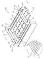
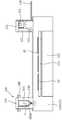
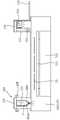
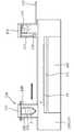
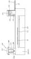
도 1은 본 실시예에 따른 전자종이 표시소자 제조장치를 나타낸 사시도이며, 도 2는 본 실시예에 따른 전자종이 표시소자 제조장치를 도 1에 표기된 Ⅰ-Ⅰ'선을 기준으로 절단한 단면도이다.1 is a perspective view showing an electronic paper display device manufacturing apparatus according to the present embodiment, Figure 2 is a cross-sectional view of the electronic paper display device manufacturing apparatus according to the present embodiment cut based on the line I-I 'shown in FIG. .
도 1 및 도 2를 참조하면, 본 실시예에 따른 전자종이 표시소자 제조장치(100)(이하, '전자종이 표시소자 제조장치'라 함.)는 격벽(11)이 형성된 기판(10)에 유전액(F)을 주입하여 전자종이 표시소자를 제조한다.1 and 2, the electronic paper display device manufacturing apparatus 100 (hereinafter, referred to as an “electronic paper display device manufacturing apparatus”) according to the present embodiment is formed on the
격벽(11)은 기판(10) 상에 셀(cell)이 형성되도록 하는 것으로, 화질에 영향을 미치지 않도록 투명한 재질로 이루어질 수 있다. 격벽(11)은 열경화성 수지 또는 UV 경화성수지로 이루어질 수 있다. 예를 들면, 격벽(11)은 폴리우레탄 아크릴레이트(PUA) 또는 폴리디메틸실록산(PDMS)로 이루어질 수 있다. 유전액(F)은 셀에 충진되는 각 셀 내부에서 전자볼이 원활하게 이동되도록 한다.The
한편, 전자종이 표시소자 제조장치(100)는 기판지지부(110), 유전액주입부(130) 가압부(151) 및 경화부(150)를 포함한다.Meanwhile, the electronic paper display
기판지지부(110)는 정렬스테이지(111)를 포함한다. 정렬스테이지(111)는 격벽(11)이 형성된 기판(10)을 지지하는 것으로, 기판(10)의 평면방향, 기판(10)의 상하방향으로 구동가능하다. 정렬스테이지에 대해서는 이미 본 출원인에 의해 출원된 "대한민국 등록특허 10-0661751;스테이지 미세정렬 장치" 출원된 바 있으므로, 상세한 설명을 생락하도록 한다. 이러한 정렬스테이지(111)에는 복수의 기판(10)을 이용하여 복수의 전자종이 표시소자를 제조하기 위하여 복수의 기판(10)이 함께 지지될 수 있다.The
유전액주입부(130)는 기판(10)으로 유전액(F)을 주입하는 것으로, 주입기(131)를 포함한다. 주입기(131)는 정렬스테이지(111)를 향해 개구되는 노즐(131a)을 포함한다. 주입기(131)는 기판(10)의 폭방향, 또는 기판(10)의 길이방향으로 유전액(F)을 선형 분사할 수 있다.The dielectric
주입기(131)는 제 1지지대(133)에 지지된다. 제 1지지대(133)는 제 1지지대승강기(135)에 지지된다. 제 1지지대승강기(135)는 제 1지지대(133)를 기판(10)의 상하방향으로 승강시킨다. 제 1지지대승강기(135)는 제 1지지대이송기(137)에 지지된다. 제 1지지대이송기(137)는 제 1지지대승강기(135)를 기판(10)의 평면방향으로 이송한다. 이와 같이 주입기(131)는 기판(10)의 상하 ??항으로 승강될 수 있으며, 기판(10)의 평면방향으로 이송될 수 있다.The
한편, 제 1지지대(133)에는 기판감지부(139)가 지지될 수 있다. 기판감지부(139)는 기판지지부(110)에 지지되는 기판(10)의 위치를 감지한다. 기판감지부(139)는 기판지지부(110)에 지지되는 기판(10)을 촬영하는 카메라를 사용할 수 있다. 상술된 정렬스테이지(111)는 기판감지부(139)에 의해 감지되는 기판(10)의 위치에 따라 주입기(131)에 대한 기판(10)의 위치를 정렬할 수 있다.Meanwhile, the
한편, 기판(10)에 유전액(F)이 주입되면, 도시되지 않은 이송장치에 의해 기판(10)을 밀봉하기 위한 밀봉시트(20)가 기판(10) 상으로 공급될 수 있다. 밀봉시트(20)는 접착성을 갖는 광 경화성 수지로써, 예컨대 자외선 광 경화성 수지로 이루어질 수 있다. 또한 밀봉시트(20)에는 투명전극필름(ITO;Indium Tin Oxide), 투명전도성필름(OCA;Optically Clear Adhesive)이 포함될 수 있다.On the other hand, when the dielectric liquid F is injected into the
가압부(151)는 기판(10) 상으로 공급되는 밀봉시트(20)를 가압하는 것으로, 밀봉시트(20)를 구름가압하도록 설치되는 롤러를 사용할 수 있다. 가압부(151)는 밀봉시트(20)의 접착성이 향상되도록 소정온도, 예컨대 80~120℃로 가열될 수 있다.The
경화부(150)는 기판(10) 상으로 공급되는 밀봉시트(20)가 경화되어 기판(10)에 접합되도록 하는 것으로, 광원(153)을 포함한다. 광원(153)은 기판(10) 상으로 광을 조사하여 밀봉시트(20)가 경화되도록 하는 것으로, 광원(153)으로부터 출사되는 광은 예컨데, 자외선 광일 수 있다. 이러한 광원(153)은 복수의 광 영역이 구획될 수 있다. 기판지지부(110)에 복수의 기판(10)이 지지될 경우, 복수의 광 영역은 개별제어되어 각각의 기판(10)에 개별 광을 조사할 수 있다. 또한, 광원(153)은 기판(10)의 폭방향, 또는 기판(10)의 길이방향의 선형 광을 방출하여 한번의 광 조사로 복수의 기판(10)에 광이 함께 입사되도록 할 수 있다.The
이러한 가압부(151)와 경화부(150)는 제 2지지대(155)에 함께 지지된다. 제 2지지대(155)는 제 2지지대승강기(157)에 지지되고, 제 2지지대승강기(157)는 제 2지지대(155)를 기판(10)의 상하방향으로 승강시킨다. 제 2지지대이송기(159)는 제 2지지대승강기(157)를 지지하고 제 2지지대승강기(157)를 기판(10)의 평면방향으로 이송한다. 이와 같이 가압부(151)와 경화부(150)는 기판(10)의 상하방향으로 승강될 수 있으며, 기판(10)의 평면방향으로 이송이 가능하다.The
한편, 제 2지지대(155)에는 배출부(170)가 지지될 수 있다. 배출부(170)는 밀봉시트(20)의 접합이 완료된 기판(10)을 흡착하여 기판지지부(110)의 외부로 배출되도록 하는 것으로, 제 2지지대(155)와 함께 승강 및 이송될 수 있다.Meanwhile, the
이하, 본 실시예에 따른 전자종이 표시소자 제조방법에 대해 설명하도록 한다.Hereinafter, an electronic paper display device manufacturing method according to the present embodiment will be described.
도 3은 본 실시예에 따른 전자종이 표시소자 제조방법을 나타낸 순서도이며, 도 4 내지 도 10은 본 실시예에 따른 전자종이 표시소자 제조공정을 나타낸 공정도이다.3 is a flowchart illustrating a method of manufacturing an electronic paper display device according to the present embodiment, and FIGS. 4 to 10 are flowcharts illustrating a process of manufacturing the electronic paper display device according to the present embodiment.
도 3 내지 도 7을 참조하면, 본 실시예에 따른 전자종이 표시소자 표시방법은 기판 지지단계(S11), 기판 감지단계(S12), 기판 정렬단계(S13), 유전액 주입단계(S14), 밀봉시트 공급단계(S15) 및 밀봉단계(S16)를 포함한다.3 to 7, the electronic paper display device display method according to the present embodiment is a substrate support step (S11), a substrate detection step (S12), a substrate alignment step (S13), dielectric fluid injection step (S14), Sealing sheet supply step (S15) and sealing step (S16) is included.
먼저, 도시되지 않은 기판 이송장치에 의해, 적어도 하나 이상의 기판(10)은 기판지지부(110)로 반입된다. 기판(10)은 정렬스테이지(111)에 지지된다. (단계;S11)First, at least one or
이어, 기판감지부(139)는 기판(10)의 위치를 감지한다. 즉, 제 1지지대(133)는 제 1지지대이송기(137)에 의해 기판(10)의 평면방향으로 이송된다. 제 1지지대(133)가 기판(10)의 평면방향으로 이송됨에 따라 기판감지부(139)는 기판(10)의 평면방향으로 이송된다. 기판감지부(139)는 기판(10)의 평면방향으로 이송되면서 기판(10)에 형성된 정렬마크(미도시)를 촬영한다. (단계;S12)Subsequently, the
이어, 정렬스테이지(111)는 기판(10)의 위치에 따라 기판(10)을 기판(10)의 평면방향 또는 기판(10)의 상하방향으로 이송하여 주입기(131)에 대한 기판(10)의 위치를 정렬한다. 그리고 제 1지지대승강기(135)는 제 1지지대승강기(135)를 승강시켜 기판(10)과 주입기(131)와의 이격거리가 조절되도록 한다. (단계;S13)Subsequently, the
이어, 제 1지지대이송기(137)는 제 1지지대(133)를 기판(10)의 평면방향으로 이송한다. 이와 함께, 주입기(131)는 유전액(F)을 기판(10)을 향해 주입한다. (단계;S14)Subsequently, the first
이어, 도시되지 않은 밀봉시트 이송장치에 의해 밀봉시트(20)가 기판(10) 상으로 공급된다.(단계;S15)Subsequently, the sealing
이어, 제 2지지대승강기(157)는 제 2지지대(155)를 승강시켜 기판(10)과 가압부(151)와의 거리, 기판(10)과 광원(153)과의 이격거리가 조절되도록 한다. 그리고 제 2지지대이송기(159)는 제 2지지대(155)를 기판(10)의 평면방향으로 이송한다. 제 2지지대(155)가 기판(10)의 평면방향으로 이송됨에 따라 밀봉시트(20)가 가압되어 밀봉시트(20)는 격벽(11)에 밀착된다. 이때, 가압부(151)는 가열되어 밀봉시트(20)의 접착성이 향상되도록 한다.Subsequently, the
이와 함께, 광원(153)으로부터 광이 출사된다. 광원(153)으로부터 출사되는 광은 밀봉시트(20)로 입사되어 밀봉시트(20)를 경화시킨다. 이와 같이 밀봉시트(20)는 가압부(151)에 의해 가열되면서 광이 입사되어 경화된다. 이에 따라 밀봉시트(20)는 격벽(11)에 접합되어 기판(10)을 밀봉시킨다. (단계;S16)At the same time, light is emitted from the
이후, 제 2지지대승강기(157)는 제 2지지대(155)를 하강시킨다. 제 2지지대가 하강됨에 따라 흡착판(170)은 밀봉시트(20)가 접합된 기판(10)에 접촉될 수 있다. 흡착판(170)은 기판(10)을 흡착한다. 제 2지지대승강기(157)는 제 2지지대(155)를 상승시키고, 제 2지지대이송기(159)는 제 2지지대(155)를 기판지지부(110)의 외측으로 이송한다. 도시되지 않은 기판 이송장치는 기판(10)을 외부로 반출한다.Thereafter, the
상술된 바와 같이, 본 실시예에 따른 전자종이 표시소자의 제조방법 및 제조장치는 밀봉시트(20)가 기판(10)을 향해 가압됨과 동시에 밀봉시트(20)를 향해 광이 입사되므로, 밀봉시트(20)의 접합에 소요되는 시간을 단축하여 유전액(F)이 휘발되는 양을 최소화 할 수 있다.As described above, in the method and manufacturing apparatus of the electronic paper display device according to the present embodiment, since the sealing
한편, 본 실시예에서, 제 1지지대(133)에는 주입기(131)가 지지되고, 제 2지지대(155)에는 가압부(151)와 광원(153)이 함께 지지되어 가압부(151)와 광원(153)이 함께 이송되는 것으로 설명하고 있으나, 다른 실시예로, 제 1지지대(133)에는 주입기(131)와 가압부(151)이 함께 지지되어 주입기(131)와 가압부(151)가 함께 이송되도록 변형실시 될 수 있다.Meanwhile, in the present embodiment, the
앞에서 설명되고, 도면에 도시된 본 발명의 실시예는 본 발명의 기술적 사상을 한정하는 것으로 해석되어서는 안 된다. 본 발명의 보호범위는 청구범위에 기재된 사항에 의하여만 제한되고, 본 발명의 기술 분야에서 통상의 지식을 가진 자는 본 발명의 기술적 사상을 다양한 형태로 개량 변경하는 것이 가능하다. 따라서 이러한 개량 및 변경은 통상의 지식을 가진 자에게 자명한 것인 한 본 발명의 보호 범위에 속하게 될 것이다.
The embodiments of the present invention described above and shown in the drawings should not be construed as limiting the technical idea of the present invention. The scope of protection of the present invention is limited only by the matters described in the claims, and those skilled in the art will be able to modify the technical idea of the present invention in various forms. Accordingly, such improvements and modifications will fall within the scope of the present invention as long as they are obvious to those skilled in the art.
100 : 전자종이 표시소자 제조장치
110 : 기판지지부111 : 정렬스테이지
130 : 유전액주입부131 : 주입기
133 : 제 1지지대135 : 제 1지지대승강기
137 : 제 1지지대이송기139 : 기판감지부
150 : 경화부151 : 가압부
153 : 광원155 : 제 2지지대
157 : 제 2지지대승강기159 : 제 2지지대이송기
170 : 흡착판100: electronic paper display device manufacturing apparatus
110: substrate support 111: alignment stage
130: dielectric fluid injection unit 131: injector
133: the first support 135: the first support lift
137: first support conveyor 139: substrate detection unit
150: hardening portion 151: pressing portion
153: light source 155: second support
157: second support lift 159: second support conveyor
170: adsorption plate
Claims (15)
Translated fromKorean상기 기판 상으로 공급되는 광 경화성 밀봉시트가 가압되는 가압단계와,
상기 밀봉시트가 광 경화되어 상기 기판이 밀봉되는 경화단계를 포함하는 것을 특징으로 하는 전자종이 표시소자 제조방법.An injection step of injecting a dielectric liquid into a substrate on which a cell is formed by a partition wall;
A pressing step of pressing the photocurable sealing sheet supplied onto the substrate;
And a curing step in which the sealing sheet is photo-cured to seal the substrate.
상기 유전액을 주입하는 유전액주입부와 상기 밀봉시트를 가압하는 가압부가 연결되어 함께 이송되는 것을 특징으로 하는 전자종이 표시소자 제조방법.The method of claim 1,
A method of manufacturing an electronic paper display device, characterized in that the dielectric liquid injection unit for injecting the dielectric liquid and a pressing unit for pressing the sealing sheet are connected and transferred together.
상기 기판의 위치를 감지하는 기판 감지단계와,
상기 기판의 위치가 정렬되는 기판 정렬단계를 더 포함하는 것을 특징으로 하는 전자종이 표시소자 제조방법.The method of claim 1,
A substrate sensing step of sensing a position of the substrate;
And a substrate alignment step of aligning the position of the substrate.
상기 밀봉시트는 자외선 광 경화성 수지이며,
상기 광원으로부터 출사되는 상기 광은 자외선 광인 것을 특징으로 하는 전자종이 표시소자 제조방법.The method of claim 1,
The sealing sheet is an ultraviolet light curable resin,
And the light emitted from the light source is ultraviolet light.
상기 기판 상으로 공급되는 광 경화성 밀봉시트를 가압하는 가압부와,
상기 기판을 향해 광을 조사하여 광 경화되는 상기 밀봉시트에 의해 상기 기판이 밀봉되도록 하는 경화부를 포함하는 것을 특징으로 하는 전자종이 표시소자 제조장치.A dielectric liquid injection unit for injecting a dielectric liquid into a substrate on which a cell is formed by a partition wall;
A pressing unit for pressing the photocurable sealing sheet supplied onto the substrate;
And a curing unit for sealing the substrate by the sealing sheet which is photocured by irradiating light toward the substrate.
상기 기판의 위치를 감지하는 기판 감지부와,
상기 기판의 위치를 정렬하는 정렬스테이지를 더 포함하는 것을 특징으로 하는 전자종이 표시소자 제조장치.8. The method of claim 7,
A substrate detecting unit detecting a position of the substrate;
And an alignment stage for aligning the position of the substrate.
상기 밀봉시트가 접합된 상기 기판을 흡착하여 상기 기판을 외부로 배출하는 배출부를 더 포함하는 것을 특징으로 하는 전자종이 표시소자 제조장치.8. The method of claim 7,
And a discharge unit for absorbing the substrate to which the sealing sheet is bonded to discharge the substrate to the outside.
상기 기판지지부는 복수의 기판을 지지하며,
상기 경화부는 상기 복수의 기판에 개별 광을 조사할 수 있도록 복수의 광 영역이 구획되고, 상기 광은 각 광 영역별로 개별 제어되는 것을 특징으로 하는 전자종이 표시소자 제조장치.8. The method of claim 7,
The substrate support portion supports a plurality of substrates,
The hardening unit is divided into a plurality of light regions so as to irradiate individual light on the plurality of substrates, the light is electronic paper display device manufacturing apparatus characterized in that the individual control for each light region.
상기 유전액을 상기 기판의 폭방향, 또는 상기 기판의 길이방향으로 선형 분사하는 것을 특징으로 하는 전자종이 표시소자 제조장치.The method of claim 7, wherein the dielectric fluid injection portion
The dielectric paper is linearly sprayed in the width direction of the substrate, or the longitudinal direction of the substrate characterized in that the electronic paper display device manufacturing apparatus.
Priority Applications (1)
| Application Number | Priority Date | Filing Date | Title |
|---|---|---|---|
| KR1020110147926AKR20130079682A (en) | 2011-12-30 | 2011-12-30 | Electronic paper display device and manufacturing method thereof |
Applications Claiming Priority (1)
| Application Number | Priority Date | Filing Date | Title |
|---|---|---|---|
| KR1020110147926AKR20130079682A (en) | 2011-12-30 | 2011-12-30 | Electronic paper display device and manufacturing method thereof |
Publications (1)
| Publication Number | Publication Date |
|---|---|
| KR20130079682Atrue KR20130079682A (en) | 2013-07-11 |
Family
ID=48992021
Family Applications (1)
| Application Number | Title | Priority Date | Filing Date |
|---|---|---|---|
| KR1020110147926ACeasedKR20130079682A (en) | 2011-12-30 | 2011-12-30 | Electronic paper display device and manufacturing method thereof |
Country Status (1)
| Country | Link |
|---|---|
| KR (1) | KR20130079682A (en) |
Cited By (9)
| Publication number | Priority date | Publication date | Assignee | Title |
|---|---|---|---|---|
| KR20170125410A (en)* | 2014-01-21 | 2017-11-14 | 카티바, 인크. | Apparatus and techniques for electronic device encapsulation |
| US10512931B2 (en) | 2014-01-21 | 2019-12-24 | Kateeva, Inc. | Apparatus and techniques for electronic device encapsulation |
| US10537911B2 (en) | 2014-04-30 | 2020-01-21 | Kateeva, Inc. | Gas cushion apparatus and techniques for substrate coating |
| US11107712B2 (en) | 2013-12-26 | 2021-08-31 | Kateeva, Inc. | Techniques for thermal treatment of electronic devices |
| KR20220114794A (en) | 2021-02-09 | 2022-08-17 | 이레이노베이션 주식회사 | Fermented salt using Bacillus strain and its manufacturing method |
| US11633968B2 (en) | 2008-06-13 | 2023-04-25 | Kateeva, Inc. | Low-particle gas enclosure systems and methods |
| US11975546B2 (en) | 2008-06-13 | 2024-05-07 | Kateeva, Inc. | Gas enclosure assembly and system |
| US12018857B2 (en) | 2008-06-13 | 2024-06-25 | Kateeva, Inc. | Gas enclosure assembly and system |
| US12064979B2 (en) | 2008-06-13 | 2024-08-20 | Kateeva, Inc. | Low-particle gas enclosure systems and methods |
- 2011
- 2011-12-30KRKR1020110147926Apatent/KR20130079682A/ennot_activeCeased
Cited By (13)
| Publication number | Priority date | Publication date | Assignee | Title |
|---|---|---|---|---|
| US11633968B2 (en) | 2008-06-13 | 2023-04-25 | Kateeva, Inc. | Low-particle gas enclosure systems and methods |
| US12344014B2 (en) | 2008-06-13 | 2025-07-01 | Kateeva, Inc. | Gas enclosure assembly and system |
| US12064979B2 (en) | 2008-06-13 | 2024-08-20 | Kateeva, Inc. | Low-particle gas enclosure systems and methods |
| US12018857B2 (en) | 2008-06-13 | 2024-06-25 | Kateeva, Inc. | Gas enclosure assembly and system |
| US11975546B2 (en) | 2008-06-13 | 2024-05-07 | Kateeva, Inc. | Gas enclosure assembly and system |
| US11107712B2 (en) | 2013-12-26 | 2021-08-31 | Kateeva, Inc. | Techniques for thermal treatment of electronic devices |
| US12040203B2 (en) | 2013-12-26 | 2024-07-16 | Kateeva, Inc. | Techniques for thermal treatment of electronic devices |
| US11489119B2 (en) | 2014-01-21 | 2022-11-01 | Kateeva, Inc. | Apparatus and techniques for electronic device encapsulation |
| KR20170125410A (en)* | 2014-01-21 | 2017-11-14 | 카티바, 인크. | Apparatus and techniques for electronic device encapsulation |
| US10512931B2 (en) | 2014-01-21 | 2019-12-24 | Kateeva, Inc. | Apparatus and techniques for electronic device encapsulation |
| US11338319B2 (en) | 2014-04-30 | 2022-05-24 | Kateeva, Inc. | Gas cushion apparatus and techniques for substrate coating |
| US10537911B2 (en) | 2014-04-30 | 2020-01-21 | Kateeva, Inc. | Gas cushion apparatus and techniques for substrate coating |
| KR20220114794A (en) | 2021-02-09 | 2022-08-17 | 이레이노베이션 주식회사 | Fermented salt using Bacillus strain and its manufacturing method |
Similar Documents
| Publication | Publication Date | Title |
|---|---|---|
| KR20130079682A (en) | Electronic paper display device and manufacturing method thereof | |
| KR101471705B1 (en) | Method and system for manufacturing display panel | |
| JP5456657B2 (en) | Method for manufacturing flat display device and laminating and pressing device therefor | |
| TW201334961A (en) | Bonding device and bonding method | |
| KR20070014844A (en) | Quartz plate support device for organic light emitting display device manufacturing | |
| JP2013200430A (en) | Substrate sticking method and substrate sticking device | |
| KR101218351B1 (en) | Apparatus and method for bonding panel | |
| JP5902525B2 (en) | Substrate bonding method and bonding apparatus | |
| CN104765167A (en) | Substrate bonding apparatus, apparatus and method for manufacturing display device member | |
| TWI581866B (en) | Adhesive dissipation apparatus and method thereof, manufacturing apparatus for member of display device and method thereof | |
| KR20160137736A (en) | A lamination equipment and method | |
| CN1713039A (en) | Apparatus and method for manufacturing liquid crystal displays | |
| CN115732617A (en) | Protective film forming apparatus | |
| JP2013199041A (en) | Method and apparatus for laminating substrates | |
| KR20130125865A (en) | Apparatus for forming flatness of glass substrate using the same | |
| JP2007121639A (en) | Panel alignment system | |
| JP5393290B2 (en) | Web processing apparatus and electronic device manufacturing method | |
| JP3022809B2 (en) | Method and apparatus for sealing liquid crystal display cell | |
| KR101111064B1 (en) | UV curing method for flat panel display device manufacturing | |
| KR100931320B1 (en) | UV curing device for flat panel display liquid crystal manufacturing | |
| KR101679560B1 (en) | Imprinting Apparatus | |
| CN104511400B (en) | Adhesive coating device and method, display device component manufacture device and method | |
| KR100965412B1 (en) | UV curing device for flat panel display device manufacturing | |
| TWI847241B (en) | Protective film forming device | |
| TWI838833B (en) | Protective film forming device |
Legal Events
| Date | Code | Title | Description |
|---|---|---|---|
| A201 | Request for examination | ||
| PA0109 | Patent application | Patent event code:PA01091R01D Comment text:Patent Application Patent event date:20111230 | |
| PA0201 | Request for examination | ||
| E902 | Notification of reason for refusal | ||
| PE0902 | Notice of grounds for rejection | Comment text:Notification of reason for refusal Patent event date:20130628 Patent event code:PE09021S01D | |
| PG1501 | Laying open of application | ||
| E601 | Decision to refuse application | ||
| PE0601 | Decision on rejection of patent | Patent event date:20140129 Comment text:Decision to Refuse Application Patent event code:PE06012S01D Patent event date:20130628 Comment text:Notification of reason for refusal Patent event code:PE06011S01I |