KR20130076703A - Information processing apparatus and method of controlling information processing apparatus - Google Patents
Information processing apparatus and method of controlling information processing apparatusDownload PDFInfo
- Publication number
- KR20130076703A KR20130076703AKR1020120130289AKR20120130289AKR20130076703AKR 20130076703 AKR20130076703 AKR 20130076703AKR 1020120130289 AKR1020120130289 AKR 1020120130289AKR 20120130289 AKR20120130289 AKR 20120130289AKR 20130076703 AKR20130076703 AKR 20130076703A
- Authority
- KR
- South Korea
- Prior art keywords
- node
- processing
- state
- processing unit
- unit
- Prior art date
- Legal status (The legal status is an assumption and is not a legal conclusion. Google has not performed a legal analysis and makes no representation as to the accuracy of the status listed.)
- Granted
Links
Images


Classifications
- G—PHYSICS
- G06—COMPUTING OR CALCULATING; COUNTING
- G06F—ELECTRIC DIGITAL DATA PROCESSING
- G06F9/00—Arrangements for program control, e.g. control units
- G06F9/06—Arrangements for program control, e.g. control units using stored programs, i.e. using an internal store of processing equipment to receive or retain programs
- G06F9/46—Multiprogramming arrangements
- G06F9/52—Program synchronisation; Mutual exclusion, e.g. by means of semaphores
- G—PHYSICS
- G06—COMPUTING OR CALCULATING; COUNTING
- G06F—ELECTRIC DIGITAL DATA PROCESSING
- G06F15/00—Digital computers in general; Data processing equipment in general
Landscapes
- Engineering & Computer Science (AREA)
- Theoretical Computer Science (AREA)
- Software Systems (AREA)
- Physics & Mathematics (AREA)
- General Engineering & Computer Science (AREA)
- General Physics & Mathematics (AREA)
- Computer Hardware Design (AREA)
- Power Sources (AREA)
- Stored Programmes (AREA)
- Multi Processors (AREA)
- Hardware Redundancy (AREA)
Abstract
Description
Translated fromKorean본 발명은 정보 처리 장치 및 정보 처리 장치의 제어 방법에 관한 것이다.The present invention relates to an information processing apparatus and a control method of the information processing apparatus.
종래부터, 연산 처리 장치 및 기억 장치를 구비한 복수의 노드를 포함하는 정보 처리 장치에서는, 복수의 노드가 구비하는 각 연산 처리 장치가 각각의 하드웨어 스레드에 있어서 실행하는 각 처리 간의 동기를 제어하는 여러 가지의 제어 방법이 있다.Background Art Conventionally, in an information processing apparatus including a plurality of nodes provided with an arithmetic processing unit and a storage unit, various arithmetic units for controlling the synchronization between each processing executed by each arithmetic processing unit included in the plurality of nodes in each hardware thread are provided. There are branch control methods.
일반적으로, 스레드는 소프트웨어에서 병렬적으로 실행되는 프로그램의 처리 단위를 말하고, 멀티스레드는 하나의 연산 처리 장치에서 복수의 스레드를 병행하여 실행하는 것을 말한다.In general, a thread refers to a processing unit of a program executed in parallel in software, and a multithread refers to executing a plurality of threads in parallel in a single processing unit.
한편, 하드웨어 스레드는 하드웨어 멀티스레딩이라는 명칭으로도 알려져 있으며, 다음과 같은 기술을 말한다. 예컨대, 하드웨어 스레드는 CPU(Central Processing Unit)가 구비하는 동일 코어 상에서, 연산기, 레지스터, TLB(Translation Look-aside Buffer), 시스템 버스 컨트롤러 등의 하드웨어 자원을 공유시키는 기술이다. 즉, 하드웨어 스레드는 동일 코어 상에서, 하드웨어 자원을 공유시켜서 복수의 스레드를 동시에 동작시키는 기술이다. 하드웨어 스레드에는, 복수의 스레드를 동시에 동작시키는 기술 외에, 시분할 처리에 의해서 복수의 스레드를 동작시키는 VMT(Vertical Multi-Threading), SMT(Simultaneous Multi-Threading) 등 각종 실장 방법이 알려져 있다.Hardware threads are also known as hardware multithreading and refer to the following techniques. For example, a hardware thread is a technology for sharing hardware resources such as an operator, a register, a translation look-aside buffer (TLB), and a system bus controller on the same core included in a central processing unit (CPU). That is, a hardware thread is a technique of operating a plurality of threads simultaneously by sharing hardware resources on the same core. In addition to the technique of operating a plurality of threads simultaneously in hardware threads, various implementation methods such as Vertical Multi-Threading (VMT) and Simultaneous Multi-Threading (SMT) for operating a plurality of threads by time division processing are known.
전술한 바와 같이 하드웨어 스레드에 있어서, 예컨대 제1 노드가 구비하는 제1 연산 처리 장치가 포함하는 제1 하드웨어 스레드에 있어서 실행중인 처리가, 제2 노드가 구비하는 제2 기억 장치가 기억하는 데이터를 필요로 하는 케이스를 생각할 수 있다.As described above, in the hardware thread, the processing executed in the first hardware thread included in the first arithmetic processing unit included in the first node, for example, stores data stored in the second storage unit included in the second node. You can think of the case you need.
전술한 케이스에서의 각 처리 간의 동기 제어 방법으로서, 예컨대 폴링 방식에 의한 제어 방법이 있다. 즉, 제1 연산 처리 장치는, 제1 하드웨어 스레드에 있어서 실행중인 처리를 중단하고, 제2 노드가 구비하는 제2 연산 처리 장치가 제1 기억 장치에 데이터를 카피하는 처리가 완료할 때까지 제1 기억 장치에 액세스하는 폴링 처리를 한다. 그리고, 제1 연산 처리 장치는, 제2 연산 처리 장치가 제1 기억 장치에 데이터를 카피하는 처리가 완료되면, 제1 기억 장치로부터 데이터를 판독하여, 제1 하드웨어 스레드에 있어서, 중단한 처리를 재개한다.As a synchronous control method between the processes in the above-described case, for example, there is a control method by a polling method. That is, the first arithmetic processing unit stops the processing being executed in the first hardware thread, and the second arithmetic processing unit until the second arithmetic processing unit included in the second node completes the process of copying data to the first storage device. 1 Polling process for accessing the storage device. When the process of copying data to the first storage device is completed, the first arithmetic processing unit reads the data from the first storage device, and stops the processing in the first hardware thread. Resume.
또한, 전술한 케이스에서의 각 처리간 동기의 다른 제어 방법으로서, 예컨대, 인터럽트 방식에 의한 제어 방법이 있다. 즉, 제1 연산 처리 장치는, 제1 하드웨어 스레드에 있어서 실행중인 처리를 중단한 후, 제2 연산 처리 장치가 제1 기억 장치에 데이터를 카피하는 처리가 완료한 것을 통지하는 인터럽트 통지를 받는다. 그러면, 제1 연산 처리 장치는 OS(Operating System)의 커넬 처리로서, 처리의 전환에 따른 레지스터 대피 처리, OS에 의한 권한 전환 처리, 제1 기억 장치로부터 데이터를 판독하기 위한 인터럽트 핸들러의 기동 처리 등의 각종 처리를 실행한다. 그리고, 제1 연산 처리 장치는 제1 기억 장치로부터 데이터를 판독하여, 제1 하드웨어 스레드에 있어서 중단한 처리를 재개한다.In addition, another control method of synchronization between the processes in the above-described case is, for example, a control method by an interrupt method. In other words, after the processing that is being executed in the first hardware thread is interrupted, the first arithmetic processing unit receives an interrupt notification for notifying that the processing for copying data to the first storage unit is completed. Then, the first arithmetic processing unit is a kernel processing of the operating system (OS), which is a register evacuation processing according to the switching of the processing, an authority switching processing by the OS, an activation processing of an interrupt handler for reading data from the first storage device, and the like. Executes various processes. The first arithmetic processing unit reads data from the first storage unit, and resumes the processing interrupted in the first hardware thread.
그러나, 전술한 종래 기술에서는, 제1 하드웨어 스레드에 있어서 처리를 중단했는데도 불구하고 제1 기억 장치에 액세스하는 폴링 처리를 한다. 이 때문에, 제1 연산 처리 장치에 있어서 다른 하드웨어 스레드와 공유하는 시스템 버스 컨트롤러 등의, 복수의 하드웨어 스레드에서 공용되는 하드웨어 자원이 유효하게 활용되지 못한다고 하는 문제가 있다.However, in the above-described prior art, the polling process for accessing the first storage device is performed despite the interruption in the first hardware thread. For this reason, there is a problem that hardware resources shared by a plurality of hardware threads, such as a system bus controller shared with other hardware threads in the first arithmetic processing unit, cannot be effectively utilized.
또한, 전술한 종래 기술에서는, 제1 하드웨어 스레드에서 실행되는 처리의 전환에 따른 레지스터의 대피 및 복원 처리 등의 OS에 의한 커넬 처리가 오버헤드가 되어 처리 전환을 신속히 행할 수 없다고 하는 문제가 있다.In addition, in the above-described prior art, there is a problem that kernel processing by the OS, such as the evacuation and restoration of registers in accordance with the switching of the processing executed in the first hardware thread, becomes overhead and the processing switching cannot be performed quickly.
일 측면에서는, 본 발명은 복수의 노드가 구비하는 각 연산 처리 장치가 각각의 처리부에서 실행하는 각 처리 간의 동기를 제어할 때에, 하드웨어 자원의 유효 활용을 도모하는 것을 목적으로 한다.In one aspect, the present invention aims to effectively utilize hardware resources when each arithmetic processing unit included in a plurality of nodes controls synchronization between respective processes executed by a respective processing unit.
개시하는 기술의 일 양태에서는, 처리를 실행하고, 상기 처리의 상태를 제어하는 처리부를 구비한 연산 처리부와, 각각 상기 연산 처리부를 구비한 복수의 노드를 포함하는 정보 처리 장치이다. 정보 처리 장치는, 상기 복수 노드의 각각은, 자기 노드가 구비하는 제1 연산 처리 장치에 포함되는 제1 처리부가 그 제1 처리부에 있어서의 처리의 상태를 제1 상태로부터 제2 상태로 이행시키는 경우에, 그 제1 처리부를 식별하는 식별 정보를 기억한다. 또한, 정보 처리 장치는, 자기 노드 또는 다른 노드가 구비하는 제2 연산 처리 장치에 포함되는 제2 처리부로부터 상기 제1 연산 처리 장치에 송신된 식별 정보를 수신한다. 또한, 정보 처리 장치는 수신한 식별 정보와, 상기 기억부가 기억하는 식별 정보가 일치하는 경우에, 그 식별 정보에 의해 식별되는 처리부가 실행하는 처리의 상태를 상기 제2 상태로부터 상기 제1 상태로 이행시키는 제어 신호를 출력한다.In one aspect of the disclosed technique, an information processing apparatus includes a calculation processing section including a processing section that executes processing and controls a state of the processing, and a plurality of nodes each having the calculation processing section. The information processing apparatus causes each of the plurality of nodes to cause the first processing unit included in the first arithmetic processing unit included in the own node to transfer the state of the processing in the first processing unit from the first state to the second state. In this case, identification information identifying the first processing unit is stored. The information processing apparatus also receives the identification information transmitted to the first arithmetic processing apparatus from the second processing unit included in the second arithmetic processing apparatus included in the own node or another node. The information processing apparatus, when the received identification information matches the identification information stored in the storage unit, changes the state of the processing executed by the processing unit identified by the identification information from the second state to the first state. The control signal to be shifted is output.
복수의 노드가 구비하는 각 연산 처리 장치가 각각의 처리부에 있어서 실행하는 각 처리 간의 동기를 제어할 때에, 하드웨어 자원의 유효 활용을 도모할 수 있다.When the arithmetic processing units included in the plurality of nodes control the synchronization between the processes executed in the respective processing units, the effective utilization of hardware resources can be achieved.
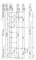
도 1은 제1 실시형태에 따른 정보 처리 장치의 구성을 도시하는 블록도이다.
도 2는 제1 실시형태에 따른 처리를 도시하는 시퀀스도이다.
도 3은 제1 실시형태에 따른 WAKEUP 패킷의 구성을 도시하는 도면이다.
도 4는 제1 실시형태에 따른 처리를 도시하는 타임차트이다.
도 5는 제1 실시형태에 따른 처리를 도시하는 플로우차트이다.
도 6은 제2 실시형태에 따른 정보 처리 장치의 구성을 도시하는 블록도이다.
도 7은 제2 실시형태에 따른 처리를 도시하는 플로우차트이다.
도 8은 제2 실시형태에 따른 WAKEUP 신호 ON 처리를 도시하는 플로우차트이다.1 is a block diagram showing the configuration of an information processing apparatus according to a first embodiment.
2 is a sequence diagram showing a process according to the first embodiment.
3 is a diagram illustrating a configuration of a WAKEUP packet according to the first embodiment.
4 is a time chart showing a process according to the first embodiment.
5 is a flowchart showing a process according to the first embodiment.
6 is a block diagram showing the configuration of an information processing apparatus according to a second embodiment.
7 is a flowchart showing a process according to the second embodiment.
8 is a flowchart showing a WAKEUP signal ON processing according to the second embodiment.
이하에, 개시하는 기술에 따른 정보 처리 장치 및 정보 처리 장치의 제어 방법의 실시형태를 도면에 기초하여 설명한다. 또, 이하의 실시형태에서는, 일례를 나타내는데 지나지 않고, 개시의 기술을 한정하는 것은 아니다. 또한, 각 실시형태는 모순이 생기지 않는 범위 내에서 적절하게 조합하더라도 좋다.EMBODIMENT OF THE INVENTION Below, embodiment of the information processing apparatus and control method of an information processing apparatus which concern on the technique disclosed is demonstrated based on drawing. In addition, in the following embodiment, it shows only an example and does not limit the technique of indication. In addition, you may combine each embodiment suitably in the range which does not produce a contradiction.
[제1 실시형태][First Embodiment]
(제1 실시형태의 정보 처리 장치의 구성)(Configuration of Information Processing Apparatus of First Embodiment)
도 1은 제1 실시형태에 따른 정보 처리 장치의 구성을 도시하는 블록도이다. 또, 이하에서는, SC는 System Controller의 약칭이고, CPU는 Central Processing Unit의 약칭이며, MAC는 Memory Access Controller의 약칭이다. 또한, IC-ctrl는 Inter Connect-Controller의 약칭이고, IC-IF는 Inter Connect Interface의 약칭이며, SVP는 Service Processor의 약칭이다.1 is a block diagram showing the configuration of an information processing apparatus according to a first embodiment. In the following description, SC stands for System Controller, CPU stands for Central Processing Unit, and MAC stands for Memory Access Controller. In addition, IC-ctrl is short for Inter Connect-Controller, IC-IF is short for Inter Connect Interface, and SVP is short for Service Processor.
또한, 이하에서 노드란, 정보 처리 유닛의 단위를 말한다. SC는 각 노드에 탑재되는 CPU와 MAC 사이의 데이터 전송 등의 처리를 제어하고, 각 노드 전체를 제어한다. MAC는 DIMM((Dual Inline Memory Module) 등의 기억 장치인 로컬 메모리, 공유 메모리와 SC 사이에 접속되어, 로컬 메모리, 공유 메모리에의 액세스를 제어한다.In addition, below, a node means the unit of an information processing unit. The SC controls processing such as data transfer between the CPU and MAC mounted in each node, and controls the entire node. The MAC is connected between the local memory, the shared memory, and the SC, which is a storage device such as a dual inline memory module (DIMM), to control access to the local memory and the shared memory.
또한, IC-ctrl는 노드간 통신을 제어하는 제어 장치이다. IC-IF는 IC-ctrl 에 의한 노드간 통신의 인터페이스이다. SVP는, 노드마다 구비되고, 각 노드의 CPU 등의 연산 처리 장치와는 독립적으로 각 노드의 하드웨어 제어 및 감시를 행하는 프로세서이며, 다른 노드가 구비하는 SVP와 LAN(Local Area Network) 등을 통해 통신을 하여 정보를 송수신한다.In addition, IC-ctrl is a control device for controlling communication between nodes. IC-IF is an interface of inter-node communication by IC-ctrl. The SVP is a processor that is provided for each node and performs hardware control and monitoring of each node independent of the arithmetic processing unit such as a CPU of each node. The SVP is a processor for communicating with the SVP of another node via a LAN (Local Area Network) And transmits and receives information.
도 1에 도시한 바와 같이, 제1 실시형태에 따른 정보 처리 장치(1)는 노드(10 및 20)를 갖는다. 노드(10)는 SC(11)를 갖는다. 노드(10)는 또한, 도 1에 있어서 일점 쇄선으로 나타내는 시스템 버스(12)를 통해 SC(11)와 각각 접속되는 CPU(13a 및 13b), MAC(14), IC-ctrl(15)를 갖는다.As shown in FIG. 1, the
노드(10)는 또한, MAC(14)과 각각 접속되는 로컬 메모리(16a), 공유 메모리(16b)를 갖는다. 노드(10)는 또한, IC-ctrl(15)와 각각 접속되는 WAKEUP 신호 생성부(17a 및 17b)를 갖는다. 노드(10)는 또한, SVP(18)를 갖는다.The
SC(11)는 CPU(13a 및 13b)에 의한 로컬 메모리(16a) 및 공유 메모리(16b) 에의 액세스 요구를 MAC(14)에 전송한다. 또한, SC(11)는 노드(20)에 의한 공유 메모리(16b)에의 액세스를 MAC(14)에 전송한다. 또한, SC(11)는 CPU(13a 및 13b)와, WAKEUP 신호 생성부(17a 및 17b) 사이에서의 정보의 입출력을 제어한다. 또한, SC(11)는 CPU(13a 및 13b)에 의한 노드(20)에의 액세스를 IC-ctrl(15)에 전송한다.The SC 11 sends an access request to the local memory 16a and the shared memory 16b by the
또한, SC(11)는 CPU(13a 및 13b)로부터 WAKEUP 신호 생성부(17a 및 17b)로의 데이터를 WAKEUP 신호 생성부(17a 및 17b)에 각각 입력한다. 또한, IC-ctrl(15)는 노드(20)로부터 WAKEUP 신호 생성부(17a 및 17b)로의 데이터를 WAKEUP 신호 생성부(17a 및 17b)에 각각 입력한다.The SC 11 also inputs data from the
노드(20)는 노드(10)와 동일한 구성이며, 참조 부호가 다른 동일 명칭의 구성 요소는 동일한 구성 및 기능을 갖는다. 노드(20)는 SC(21), 시스템 버스(22), CPU(23a 및 23b), MAC(24), IC-ctrl(25), 로컬 메모리(26a), 공유 메모리(26b), WAKEUP 신호 생성부(27a 및 27b), SVP(28)를 갖는다.The node 20 has the same configuration as the
노드(20)에 있어서의 SC(21), 시스템 버스(22), CPU(23a 및 23b), MAC(24), IC-ctrl(25)는 노드(10)에 있어서의 SC(11), 시스템 버스(12), CPU(13a 및 13b), MAC(14), IC-ctrl(15)에 각각 대응한다. 또한, 노드(20)에 있어서의 로컬 메모리(26a), 공유 메모리(26b), SVP(28)는 노드(10)에 있어서의 로컬 메모리(16a), 공유 메모리(16b), SVP(18)에 각각 대응한다. 또한, 노드(20)에 있어서의 WAKEUP 신호 생성부(27a 및 27b)는 노드(10)에 있어서의 WAKEUP 신호 생성부(17a 및 17b)에 각각 대응한다.The
노드(10 및 20)는 IC-IF(3)를 통해 IC-ctrl(15) 및 IC-ctrl(25)이 접속되는 것에 의해, 상호 통신이 가능하다. 또한, 노드(10)의 SVP(18) 및 노드(20)의 SVP(28)는 정해진 통신 회선을 통해 접속되는 것에 의해, 상호 통신이 가능하다.The
(제1 실시형태의 CPU 및 WAKEUP 신호 생성부의 구성)(Configuration of CPU and WAKEUP Signal Generation Unit in First Embodiment)
CPU(23a)를 대표로 하여, CPU(13a, 13b, 23a 및 23b)의 구성을 설명한다. 즉, CPU(13a, 13b 및 23b)의 구성은 CPU(23a)의 구성과 동일하다. 또한, WAKEUP 신호 생성부(27a)를 대표로 하여, WAKEUP 신호 생성부(17a, 17b, 27a 및 27b)의 구성을 설명한다. 즉, WAKEUP 신호 생성부(17a, 17b 및 27b)의 구성은 WAKEUP 신호 생성부(27a)의 구성과 동일하다.The configuration of the
도 1에 도시한 바와 같이, CPU(23a)는, 예컨대 멀티코어 CPU이며, 멀티코어 CPU에 포함되는 각 CPU 코어가 하드 스레드(23a-1 및 23a-2)에 해당한다. 하드 스레드는 하드웨어 스레드의 약칭이다. 하드 스레드(23a-1 및 23a-2)는 CPU(23a)의 동일 코어 상에서, CPU(23a)의 하드웨어 자원을 공유하여 각각이 처리를 실행한다.As shown in FIG. 1, the
또한, CPU(23a)는 하드 스레드(23a-1 및 23a-2)가 시스템 버스(22)를 통해서 CPU(23a)에 의해 행해지는 데이터의 입출력을 제어하는 인터페이스인, SC(21)에 접속되는 시스템 버스 컨트롤러(23a-3)를 갖는다. 즉, 시스템 버스컨트 롤러(23a-3)는 하드 스레드(23a-1 및 23a-2)에 의해 공유되는 입출력 인터페이스이다.In addition, the
또한, 도 1에 도시한 바와 같이, WAKEUP 신호 생성부(27a)는 SleepID 레지스터(27a-1 및 27a-2), WAKEUP 데이터 레지스터(27a-3), 비교부(27a-5 및 27a-6), AND부(27a-7 및 27a-8)를 갖는다. SleepID는 Sleep Identifier의 약칭이다. SleepID는 각 하드 스레드(23a-1 및 23a-2)를 식별하는 식별 정보이다. SleepID는 각 하드 스레드(23a-1 및 23a-2)가 처리 실행중에 데이터의 입력 대기가 발생하여 처리를 중단하는 경우에, 대응하는 WAKEUP 신호 생성부(27a 및 27b)에 각각 출력된다.1, the
또, SleepID 레지스터(27a-1), 비교부(27a-5), AND부(27a-7)는 CPU(23a)의 하드 스레드(23a-1)에 대응하여 설치된다. 마찬가지로, SleepID 레지스터(27a-2), 비교부(27a-6), AND부(27a-8)는 CPU(23a)의 하드 스레드(23a-2)에 대응하여 설치된다.The
SleepID 레지스터(27a-1)는 하드 스레드(23a-1)에 의해 WAKEUP 신호 생성부(27a)에 대하여 출력되는 SleepID를 기억하는 레지스터이다. 하드 스레드(23a-1)를 식별하는 SleepID는 하드 스레드(23a-1)로부터 출력되며, 시스템 버스 컨트롤러(23a-3), SC(21)를 경유하여 시스템 버스(22)를 통해 전송되어, SleepID 레지스터(27a-1)에 설정된다.The
마찬가지로, SleepID 레지스터(27a-2)는 하드 스레드(23a-2)에 의해 WAKEUP 신호 생성부(27a)에 대하여 출력되는 SleepID를 기억하는 레지스터이다. 하드 스레드(23a-2)를 식별하는 SleepID는 하드 스레드(23a-2)로부터 출력되며, 시스템 버스 컨트롤러(23a-3), SC(21)를 경유하여 시스템 버스(22)를 통해 전송되어, SleepID 레지스터(27a-2)에 설정된다.Similarly, the
또, 노드(20)가 구비하는 CPU(23a 및 23b)의 각 하드 스레드를 식별하는 각각의 SleepID는 노드(20)의 시스템 기동 시에, SVP(28)에 의해 노드(10)의 SVP(18)에 미리 통지된다. SVP(18)는 SVP(28)로부터 통지된 노드(20)의 CPU(23a 및 23b)의 각 하드 스레드를 식별하는 각각의 SleepID를, 도시하지 않는 메모리에 기억시켜, 노드(10)의 CPU(13a 및 13b)의 각 하드 스레드를 이용할 수 있는 상태로 해 둔다.In addition, each SleepID identifying each hard thread of the
또는, 노드(20)가 구비하는 CPU(23a 및 23b)의 각 하드 스레드를 식별하는 각각의 SleepID는 각 하드 스레드가 실행하는 처리마다 노드(10)에 통지되는 것으로 해도 좋다. 또는, 각 하드 스레드가 실행하는 처리에 데이터의 입력 대기가 발생했을 때에 대응하는 SleepID 레지스터에 설정되는 SleepID를 출력할 때에, 노드(10)에 통지되는 것으로 해도 좋다. 통지된 SleepID는, 예컨대 SC(11)에 의해 MAC(14)를 통해 로컬 메모리(16a) 등에 기억되어, 노드(10)의 CPU(13a 및 13b)의 각 하드 스레드를 이용할 수 있는 상태로 해 두는 것으로 해도 좋다.Alternatively, each SleepID identifying each hard thread of the
WAKEUP 데이터 레지스터(27a-3)는, 노드(10)의 CPU(13a 및 13b)로부터 IC-IF(3) 및 IC-ctrl(25)를 경유하여 통지된 WAKEUP 데이터가 포함하는 SleepID가 설정되는 레지스터이다. WAKEUP 데이터는 노드(10)의 CPU(13a 및 13b)가 실행하는 정해진 처리를 완료한 것을 노드(20)의 CPU(23a 및 23b)에 통지하는 데이터이다. 정해진 처리란, 예컨대 노드(10)의 CPU(13a 또는 13b)의 하드 스레드가, CPU(23a)의 하드 스레드(23a-1 또는 23a-2)가 기다리는 데이터를 노드(10)의 로컬 메모리(16a)로부터 노드(20)의 공유 메모리(26b)에 카피하는 처리이다.The WAKEUP data register 27a-3 is a register to which a SleepID contained in the WAKEUP data notified from the
노드(20)의 CPU(23a 및 23b)는 하드 스레드를 정지해서 CPU(23a 및 23b)가 실행하는 정해진 처리의 완료를 기다리고, CPU(13a 및 13b)로부터 WAKEUP 데이터가 통지되면, 정지한 하드 스레드를 기동한다. 그리고, CPU(23a 및 23b)는 시스템 버스 컨트롤러(23a-3), SC(21)를 통해 공유 메모리(26b)에 카피된 데이터를 취득하고, 중단한 처리를 재개한다.The
비교부(27a-5)는 WAKEUP 데이터 레지스터(27a-3) 및 SleepID 레지스터(27a-1)에 설정된 SleepID를 비교한다. 그리고, 비교부(27a-5)는 WAKEUP 데이터 레지스터(27a-3) 및 SleepID 레지스터(27a-1)에 설정된 SleepID가 일치하는 경우에, 셀렉트 신호를 AND부(27a-7)에 출력한다.The comparing
AND부(27a-7)는 비교부(27a-5)로부터 출력된 셀렉트 신호와, 노드(10)의 CPU(13a 및 13b)로부터 WAKEUP 데이터가 통지된 타이밍에 IC-ctrl(25)로부터 출력된 패킷 수신 펄스와의 논리곱을 취하는 논리 게이트이다. 패킷 수신 펄스는 WAKEUP 패킷을 수신했을 때에, IC-ctrl(25)에 의해 1펄스 발생한다.The AND
AND부(27a-7)는 셀렉트 신호와 패킷 수신 펄스의 논리곱을 나타내는 신호를 하드 스레드(23a-1)에 출력한다. 즉, AND부(27a-7)는 통지된 SleepID와, SleepID 레지스터(27a-1)에 설정된 SleepID가 일치하는 경우에, 하드 스레드(23a-1)에 정지를 해제하여 기동하고 처리를 재개하는 지시를 출력한다. 하드 스레드(23a-1)는 이 지시에 따라서, 정지를 해제하여 기동하고 처리를 재개한다. 즉, 패킷 수신 펄스와 셀렉트 신호의 논리곱으로부터 생성되는 WAKEUP 신호가 1펄스만 ON이 됨으로써, 하드 스레드(23a-1)가 정지 상태를 해제한다.The AND
마찬가지로, 비교부(27a-6)는 WAKEUP 데이터 레지스터(27a-3) 및 SleepID 레지스터(27a-2)에 설정된 SleepID를 비교한다. 그리고, 비교부(27a-6)는 WAKEUP 데이터 레지스터(27a-3) 및 SleepID 레지스터(27a-2)에 설정된 SleepID가 일치하는 경우에, 셀렉트 신호를 AND부(27a-8)에 출력한다.Similarly, the
AND부(27a-8)는 비교부(27a-6)로부터 출력된 셀렉트 신호와, 노드(10)의 CPU(13a 및 13b)로부터 WAKEUP 데이터가 통지된 타이밍에 IC-ctrl(25)로부터 출력된 패킷 수신 펄스와의 논리곱을 취하는 논리 게이트이다. AND부(27a-8)는 셀렉트 신호와 패킷 수신 펄스의 논리곱을 나타내는 신호를 하드 스레드(23a-2)에 출력한다. 즉, AND부(27a-8)는 통지된 SleepID와, SleepID 레지스터(27a-2)에 설정된 SleepID가 일치하는 경우에, 하드 스레드(23a-2)에 정지를 해제하여 기동하고 처리를 재개하는 지시를 출력한다. 하드 스레드(23a-2)는 이 지시에 따라서, 정지를 해제하여 기동하고 처리를 재개한다.The AND
(제1 실시형태의 처리의 시퀀스)(Sequence of Processing in First Embodiment)
도 2는 제1 실시형태에 따른 처리를 도시하는 시퀀스도이다. 도 2는 노드(20)의 하드 스레드(23a-1)가 처리의 실행중에 노드(10)가 유지하는 데이터를 필요로 하고, 그 데이터가 노드(10)의 CPU(13a)에 의해 노드(20)의 공유 메모리(26b)에 카피되는 처리가 완료할 때까지 기다리는 예를 도시한다. 그러나, 도 2는 일례를 도시하는 것에 지나지 않고, 노드(10 또는 20)의 하드 스레드가 처리의 실행중에, 노드(10 또는 20)의 다른 CPU에 의한 처리가 완료할 때까지 기다리는 경우라면, 같은 처리가 된다.2 is a sequence diagram showing a process according to the first embodiment. 2 shows that the
우선, 예컨대 정보 처리 장치(1) 또는 노드(20)의 기동시에, 노드(20)의 SVP(28)는 노드(20)가 구비하는 모든 하드 스레드의 SleepID를, 노드(10)의 SVP(18)에 통지한다(단계 S11). 또, 단계 S11은 정보 처리 장치(1) 또는 각 노드의 기동시 등에 있어서, 각 노드의 SVP가 자기 노드 내의 각 하드 스레드의 식별 정보인 SleepID를, 각 하드 스레드에서의 처리의 실행에 앞서서 다른 노드에 미리 통지하는 처리이다.First, for example, when the
계속해서, 노드(20)의 하드 스레드(23a-1)는 하드 스레드(23a-1)의 SleepID를 WAKEUP 신호 생성부(27a)의 SleepID 레지스터(27a-1)에 설정한다(단계 S12). 계속해서, 하드 스레드(23a-1)는 스레드를 정지한다(단계 S13).Subsequently, the
한편, 노드(10)의 CPU(13a)는 노드(20)의 하드 스레드(23a-1)가 입력을 기다리는, 노드(10)의 로컬 메모리(16a)에 기억되는 데이터를 노드(20)의 공유 메모리(26b)에 카피하는 처리를 하고, 처리를 완료한다(단계 S14). 계속해서, CPU(13a)는 하드 스레드(23a-1)의 SleepID와, 하드 스레드(23a-1)를 구비하는 CPU(23a)의 CPUID를 포함하는 WAKEUP 커맨드를 발행하여, IC-ctrl(15)에 출력한다(단계 S15). 단계 S15의 처리에 의해, CPU(13a)는 처리가 종료된 것을 노드(20)의 하드 스레드(23a-1)에 통지한다.On the other hand, the
계속해서, 노드(10)의 IC-ctrl(15)는 CPU(13a)가 발행한 WAKEUP 커맨드에 기초하여, 예컨대 도 3에 도시하는 CPUID 및 WAKEUP 데이터를 갖는 WAKEUP 패킷을 생성하고, 노드(20)의 IC-ctrl(25)에 송신한다(단계 S16). 또, CPUID는 Central Processing Unit Identifier의 약칭이며, CPU를 식별하는 정보이다. CPUID로부터, 네트워크 중계 장치에 의해 송신처의 CPU를 구비한 노드가 판정되어, WAKEUP 패킷은 원하는 노드에 도달한다. 또한, WAKEUP 데이터는 단계 S11에서 노드(20)의 SVP(28)에 의해 미리 통지된 하드 스레드(23a-1)의 SleepID를 적어도 포함하는 데이터이다.Subsequently, the IC-
IC-ctrl(25)는 IC-ctrl(15)로부터 WAKEUP 패킷을 수신하면, WAKEUP 데이터가 포함하는 SleepID를 WAKEUP 데이터 레지스터(27a-3)에 기록하고, 패킷 수신 펄스를 AND부(27a-7)에 출력한다(단계 S17). 계속해서, WAKEUP 신호 생성부(27a)는 WAKEUP 신호를 하드 스레드(23a-1)에 출력한다(단계 S18). 계속해서, 하드 스레드(23a-1)는 WAKEUP 신호를 수신하면, 정지한 스레드를 기동한다(단계 S19).When the IC-
(제1 실시형태의 처리 타임차트)(Processing Time Chart of the First Embodiment)
도 4는 제1 실시형태에 따른 처리를 도시하는 타임차트이다. 도 4에서는, CPU(23a)의 하드 스레드(23a-1 및 23a-2)가, 각각 실행하는 처리에 필요한 데이터의 입출력에 관해서, 시스템 버스 컨트롤러(23a-3)를 교대로 사용하는 것을 전제로 한다. 각각 실행하는 처리에 필요한 데이터는, 예컨대 로컬 메모리(26a)가 기억하는 프로그램의 데이터, 공유 메모리(26b)가 기억하는 데이터이다.4 is a time chart showing a process according to the first embodiment. In FIG. 4, the
도 4는 노드(20)의 하드 스레드(23a-1)가 처리의 실행중에 노드(10)가 유지하는 데이터를 필요로 하고, 그 데이터가 노드(10)의 CPU(13a)에 의해 노드(20)의 공유 메모리(26b)에 카피되는 처리가 완료할 때까지 기다리는 예를 도시한다. 그러나, 도 4는 일례를 도시하는 것에 지나지 않고, 노드(10 또는 20)의 다른 하드스레드가 처리의 실행중에 노드(10 또는 20)의 다른 CPU에 의한 처리가 완료할 때까지 기다리는 경우라면, 같은 처리가 된다. 또, 도 4에 있어서, 시스템 버스 컨트롤러(23a-3)의 표시 우측에 있는 "1"의 표시는 하드 스레드(23a-1)로부터 시스템 버스 컨트롤러(23a-3)에의 액세스를 나타내고, "2"의 표시는 하드 스레드(23a-2)로부터 시스템 버스 컨트롤러(23a-3)에의 액세스를 나타낸다.4 shows that the
시각 t1에 있어서, 노드(10)의 CPU(13a)는, 노드(20)의 CPU(23a)의 하드 스레드(23a-1)가 처리에 필요로 하는 데이터를 노드(20)의 공유 메모리(26b)에 카피하는 처리를 시작한다. 시각 t2에 있어서, 하드 스레드(23a-1)는 CPU(13a)가 공유 메모리(26b)에 카피하는 데이터를 필요로 하지만, 데이터의 카피가 완료되지 않기 때문에 처리를 계속할 수 없어, 데이터의 대기 상태가 된다. 그리고, 하드 스레드(23a-1)는 스레드를 정지한다.At the time t1, the
하드 스레드(23a-1)가 스레드를 정지하면, 시스템 버스 컨트롤러(23a-3)는 하드 스레드(23a-1)로부터 액세스되지 않게 되고, 다른 처리를 실행중인 하드 스레드(23a-2)만으로부터 액세스되는 점유 상태가 된다. 그리고, 시각 t3에 있어서, CPU(13a)는 하드 스레드(23a-1)가 기다리는 데이터의 카피가 완료되면, WAKEUP 커맨드를 발행하여 하드 스레드(23a-1)를 기동시킨다. 하드 스레드(23a-1)는 WAKEUP 커맨드에 따라서 기동하면, 처리를 재개하여, 시스템 버스 컨트롤러(23a-3)를 통해 공유 메모리(26b)에 카피된 데이터를 취득한다.When the
(제1 실시형태의 처리의 플로우차트)(Flowchart of Processing of First Embodiment)
도 5는 제1 실시형태에 따른 처리를 도시하는 플로우차트이다. 도 5는 노드(20)의 하드 스레드(23a-1)가 처리의 실행중에 노드(10)가 유지하는 데이터를 필요로 하고, 그 데이터가 노드(10)의 CPU(13a)에 의해 노드(20)의 공유 메모리(26b)에 카피되는 처리가 완료될 때까지 기다리는 예를 도시한다. 그러나, 도 5는 일례를 도시하는 것에 지나지 않고, 노드(10 또는 20)의 하드 스레드가 처리의 실행중에, 노드(10 또는 20)의 다른 CPU에 의한 처리가 완료될 때까지 기다리는 경우라면, 같은 처리가 된다.5 is a flowchart showing a process according to the first embodiment. FIG. 5 shows that the
우선, 노드(10)는 SVP(18)에 의해 노드(20)의 SVP(28)로부터 송신되며, 노드(20)가 구비하는 CPU(23a 및 23b)의 각 하드 스레드를 식별하는 SleepID를 수신한다(단계 S101). 또, 단계 S101은 정보 처리 장치(1) 또는 각 노드의 기동시 등에 있어서, 각 노드의 SVP가 자기 노드 내의 각 하드 스레드의 식별 정보인 SleepID를 각 하드 스레드에서의 처리의 실행에 앞서서 다른 노드에 미리 통지하는 처리이다.First, the
계속해서, 노드(10)는 MAC(14)에 의해, 노드(10)가 유지하는, CPU(23a)의 하드 스레드(23a-1)가 카피를 기다리는 데이터를, 노드(20)의 공유 메모리(26b)에 카피하는 프로세스 처리를 실행한다(단계 S102). 또, 단계 S102의 처리는 MAC(14)에 설치된 도시하지 않는 DMA 컨트롤러에 의해 실행되더라도 좋다.Subsequently, the
계속해서, 노드(10)는 CPU(13a)에 의해, 단계 S102의 처리가 종료되었는지 여부를 판정한다(단계 S103). 단계 S102의 처리가 종료되었다고 판정된 경우(단계 S103 Yes), 노드(10)는 단계 S104로 처리를 이행한다. 한편, 단계 S102의 처리가 종료되었다고 판정되지 않은 경우(단계 S103 No), 노드(10)는 단계 S102로 처리를 이행하고, MAC(14) 또는 도시하지 않는 DMA 컨트롤러 등에 의한 단계 S102의 프로세스 처리를 계속한다.Subsequently, the
계속해서, 노드(10)는 CPU(13a)에 의해 CPUID와 SleepID를 지정하여 WAKEUP 커맨드를 발행한다(단계 S104). 여기서는, 예컨대 CPUID로서 노드(20)의 CPU(23a)의 ID, SleepID로서 하드 스레드(23a-1)의 SleepID를 지정한다. 계속해서, 노드(10)는 CPU(13a)에 의해, 단계 S104에서 발행한 WAKEUP 커맨드에 따른 WAKEUP 패킷을 생성하여, 노드(20)에 송신한다(단계 S105).Subsequently, the
한편, 노드(20)는 SVP(28)에 의해, 노드(20)가 구비하는 CPU(23a 및 23b)의 각 하드 스레드를 식별하는 SleepID를 노드(10)의 SVP(18)에 송신한다(단계 S201). 또, 단계 S201은 정보 처리 장치(1) 또는 각 노드의 기동시 등에 있어서, 각 노드의 SVP가 자기 노드 내의 각 하드 스레드의 식별 정보인 SleepID를, 각 하드 스레드에서의 처리의 실행에 앞서서 다른 노드에 미리 통지하는 처리이다.On the other hand, the node 20 transmits, to the
계속해서, 노드(20)는 CPU(23a 및 23b)의 각 하드 스레드에 의해, 각각의 프로세스 처리를 실행한다(단계 S202). 계속해서, 노드(20)는 CPU(23a 및 23b)의 각 하드 스레드에 의해, 단계 S202의 프로세스 처리의 실행중에서, 노드(10)에 있어서의 단계 S102의 프로세스 처리가 완료되는 것을 기다리는지 여부를 판정한다(단계 S203).Subsequently, the node 20 executes respective process processing by each hard thread of the
노드(10)에 있어서의 단계 S102의 처리가 완료되는 것을 기다린다고 판정된 경우(단계 S203 Yes), 노드(20)는 단계 S204로 처리를 이행한다. 노드(10)에 있어서의 단계 S102의 프로세스 처리가 완료되는 것을 기다린다고 판정되지 않은 경우(단계 S203 No), 노드(20)는 단계 S202로 처리를 이행하고, 각 하드 스레드에 의해 프로세스 처리를 계속한다. 여기서는, 예컨대 노드(10)에 있어서의 단계 S102의 프로세스 처리가 완료되는 것을 기다린다고 판정된 하드 스레드가 하드 스레드(23a-1)이다.If it is determined that the process of step S102 in the
계속해서, 노드(20)는 노드(10)에 있어서의 프로세스 처리의 완료를 기다리는 하드 스레드(23a-1)에 의해, SleepID 레지스터(27a-1)에 하드 스레드(23a-1)의 SleepID를 설정한다(단계 S204). 계속해서, 노드(20)는 하드 스레드(23a-1)에 의해 실행중인 프로세스를 중단하고(중단한 프로세스를, 이하 중단 프로세스라고 부른다), 스레드를 정지한다(단계 S205).Subsequently, the node 20 sets the SleepID of the
계속해서, 노드(20)는 WAKEUP 신호 생성부(27a)에 의해, 노드(10)로부터 WAKEUP 패킷을 수신했는지 여부를 판정한다(단계 S206). 노드(10)로부터 WAKEUP 패킷을 수신했다고 판정된 경우(단계 S206 Yes), 노드(20)는 단계 S207로 처리를 이행한다. 한편, WAKEUP 패킷을 수신했다고 판정되지 않은 경우(단계 S206 No), 노드(20)는 단계 S206을 반복한다.Subsequently, the node 20 determines whether or not the WAKEUP packet has been received from the
계속해서, 노드(20)는 WAKEUP 신호 생성부(27a)에 의해, WAKEUP 패킷의 WAKEUP 데이터를 WAKEUP 데이터 레지스터(27a-3)에 설정한다(단계 S207).Subsequently, the node 20 sets the WAKEUP data of the WAKEUP packet to the WAKEUP data register 27a-3 by the WAKEUP
계속해서, 노드(20)는 비교부(27a-5)에 의해, SleepID 레지스터(27a-1)의 값과, WAKEUP 데이터 레지스터(27a-3)의 WAKEUP 데이터에 포함되는 SleepID가 같은지 여부를 판정한다(단계 S208). SleepID 레지스터(27a-1)의 값과, WAKEUP 데이터 레지스터(27a-3)의 WAKEUP 데이터에 포함되는 SleepID가 같다고 판정된 경우(단계 S208 Yes), 노드(20)는 단계 S209로 처리를 이행한다. SleepID 레지스터(27a-1)의 값과, WAKEUP 데이터 레지스터(27a-3)의 WAKEUP 데이터에 포함되는 SleepID가 같다고 판정되지 않은 경우(단계 S208 No), 노드(20)는 단계 S206으로 처리를 이행한다.Subsequently, the node 20 determines whether the value of the
계속해서, 노드(20)는 AND부(27a-7)에 의해 WAKEUP 신호를 생성하여 하드 스레드(23a-1)에 출력한다(단계 S209). 계속해서, 노드(20)는 하드 스레드(23a-1)에 의해, WAKEUP 신호의 출력에 응답하여, 단계 S205에서 정지된 하드 스레드를 기동시켜(단계 S210), 중단 프로세스를 재개한다(단계 S211).Subsequently, the node 20 generates a WAKEUP signal by the AND
(제1 실시형태에 의한 효과)(Effects according to the first embodiment)
CPU 내에서, 시스템 버스 컨트롤러를 공유하는 하드 스레드의 일부가 정지중, 정해진 주기로 CPU의 자원을 사용하는 폴링 방식에 비교하여, 다른 하드 스레드가 시스템 버스 컨트롤러 등의 CPU 자원을 점유할 수 있다. 따라서, 다른 하드 스레드가 처리를 보다 많이 실행할 수 있게 된다. 또한, 인터럽트 방식에 비교하여, 프로세스 재개시의 OS 처리에 의한 레지스터 대피 및 복귀 처리가 필요하지 않기 때문에, 하드 스레드의 기동 및 프로세스의 재개에 요하는 시간을 단축시킬 수 있다. 또한, SleepID를 하드 스레드에 대하여 고정으로 함으로써, 프로세스 사이에서 SleepID를 통지하지 않더라도 하드 스레드의 기동을 지시할 수 있다.Within the CPU, other hard threads may occupy CPU resources, such as the system bus controller, as compared to a polling scheme in which some of the hard threads sharing the system bus controller are stopped and use the resources of the CPU at predetermined intervals. Thus, other hard threads can execute more processing. In addition, compared with the interrupt method, since the register evacuation and return processing by the OS processing at the process restart is not necessary, the time required for starting the hard thread and restarting the process can be shortened. In addition, by fixing the SleepID to the hard thread, the startup of the hard thread can be instructed without notifying the SleepID between processes.
또한, SleepID를 지정하여, WAKEUP 신호에 의한 통지를 함으로써, 특정한 하드 스레드 상의 프로세스를 기동하거나, 정지하거나 할 수 있다. 그 때문에, 잘못 해서 다른 프로세스가 기동하거나, 정지하거나 하는 것을 방지할 수 있다. 또한, CPUID를 지정함으로써, 하드 스레드의 프로세스를 기동하기 때문에, 각 CPU 간의 통신 프로세스의 동기를 제어할 수 있다.In addition, by specifying a SleepID and notifying by a WAKEUP signal, a process on a specific hard thread can be started or stopped. Therefore, it is possible to prevent another process from starting or stopping by mistake. In addition, by specifying the CPUID, the process of the hard thread is started, and therefore, the synchronization of the communication process between the CPUs can be controlled.
[제2 실시형태][Second Embodiment]
제2 실시형태에 따른 정보 처리 장치의 구성 요소에 관해서, 제1 실시형태에 따른 정보 처리 장치와 동일한 기능 및 처리의 구성 요소에는 동일한 명칭 및 참조 부호를 부여하여 설명을 생략하고, 다른 기능 및 처리의 구성 요소에 관해서만 설명한다.Regarding the components of the information processing apparatus according to the second embodiment, the same functions and components as those of the information processing apparatus according to the first embodiment are assigned the same names and reference numerals, and descriptions thereof are omitted. Only the components of the will be described.
(제2 실시형태의 정보 처리 장치의 구성)(Configuration of Information Processing Apparatus of Second Embodiment)
도 6은 제2 실시형태에 따른 정보 처리 장치의 구성을 도시하는 블록도이다. 도 6에 도시한 바와 같이, 제2 실시형태에 따른 정보 처리 장치(2)는 노드(30 및 40)를 갖는다. 노드(30)는 제1 실시형태에 따른 정보 처리 장치(1)의 노드(10)와 비교하여, WAKEUP 신호 생성부(17a) 대신에 WAKEUP 신호 생성부(37a 및 38a)를 갖는다. 또한, 노드(30)는 WAKEUP 신호 생성부(17b) 대신에 WAKEUP 신호 생성부(37b 및 38b)를 갖는다.6 is a block diagram showing the configuration of an information processing apparatus according to a second embodiment. As shown in Fig. 6, the
노드(40)는 노드(30)와 동일한 구성이며, 참조 부호가 다른 동일 명칭의 구성 요소는 동일한 구성 및 기능을 갖는다. 노드(40)는 제1 실시형태에 따른 정보 처리 장치(1)의 노드(20)와 비교하여, WAKEUP 신호 생성부(27a) 대신에 WAKEUP 신호 생성부(47a 및 48a)를 갖는다. 또한, 노드(40)는 WAKEUP 신호 생성부(27b) 대신에 WAKEUP 신호 생성부(47b 및 48b)를 갖는다.The node 40 has the same configuration as the node 30, and components having the same name with different reference numerals have the same configuration and function. The node 40 has
(제2 실시형태의 WAKEUP 신호 생성부의 구성)(Configuration of WAKEUP Signal Generating Unit of Second Embodiment)
WAKEUP 신호 생성부(47a)를 대표로 하여, WAKEUP 신호 생성부(37a, 37b, 47a 및 47b)의 구성을 설명한다. 즉, WAKEUP 신호 생성부(37a, 37b 및 47b)의 구성은 WAKEUP 신호 생성부(47a)의 구성과 동일하다.The configuration of the
도 6에 도시한 바와 같이, WAKEUP 신호 생성부(47a)는 SleepID 레지스터(27a-1), WAKEUP 데이터 레지스터(27a-3), 비교부(27a-5), AND부(27a-7), 타이머(27a-9) 및 OR부(27a-11)를 갖는다. WAKEUP 신호 생성부(47a)는 하드 스레드(23a-1)에 대응하여 설치된다. 마찬가지로, WAKEUP 신호 생성부(48a)는 하드 스레드(23a-2)에 대응하여 설치된다. 마찬가지로, WAKEUP 신호 생성부(47b 및 48b)는 CPU(23b)에 구비되는 각 하드 스레드에 대응하여 설치된다.As shown in FIG. 6, the
CPU(13a, 13b, 23a 및 23b)의 각 하드 스레드는 각각에 대응하는 WAKEUP 데이터 레지스터의 내용을 판독한다. WAKEUP 신호 생성부(37a∼48b)에 있어서, 수신한 WAKEUP 데이터와, 각 WAKEUP 신호 생성부 각각의 SleepID 레지스터의 SleepID가 일치하는 경우에, 이 SleepID가 각 WAKEUP 데이터 레지스터에 기록된다. 이에 따라, 복수의 하드 스레드가 처리 대기 상태가 되었을 때, 각 하드 스레드는 대응하는 WAKEUP 데이터 레지스터에 액세스하여, 자기 하드 스레드를 목적지로 하는 WAKEUP 데이터가 수신된 것을 확인할 수 있다. 또한, WAKEUP 데이터 레지스터에 기록된 WAKEUP 데이터가 대응하는 하드 스레드에 의해 판독되기 이전에, 다른 하드 스레드를 목적지로 하는 WAKEUP 데이터로 WAKEUP 데이터 레지스터가 갱신되어 버리는 것을 막는다.Each hard thread of the
타이머(27a-9)는 하드 스레드(23a-1)가 처리의 실행중에 데이터의 입력 대기가 발생하여 처리를 중단할 때 하드 스레드(23a-1)의 SleepID를 출력하는 경우에, 시스템 버스(22)를 경유하여 타이머 값을 설정하는 타이머이다. 타이머(27a-9)는 정해진 타이머 값이 설정되면, 정해진 시간 간격으로 타이머 값을 감산하여, 타이머 값이 0이 되면 ON 신호를 OR부(27a-11)에 출력한다.The
제2 실시형태에서는, AND부(27a-7)는 비교부(27a-5)로부터 출력된 셀렉트 신호와, IC-ctrl(25)로부터 출력된 패킷 수신 펄스와의 논리곱을 나타내는 신호를 OR부(27a-11)에 출력한다. OR부(27a-11)는 AND부(27a-7)로부터 출력된 논리곱을 나타내는 신호와, 타이머(27a-9)로부터 출력된 ON 신호와의 논리합을 취하는 논리 게이트이다. 즉, OR부(27a-11)는 타이머(27a-9)가 정해진 시간을 계시한 경우에, 하드 스레드(23a-1)에 정지를 해제하여 기동하고 처리를 재개하는 지시를 출력한다. 또는, OR부(27a-11)는 통지된 SleepID와, SleepID 레지스터(27a-1)에 설정된 SleepID가 일치하는 경우에, 하드 스레드(23a-1)에 정지를 해제하여 기동하고 처리를 재개하는 지시를 출력한다. 하드 스레드(23a-1)는 이 지시에 따라서 정지를 해제하여 기동하고 처리를 재개한다.In the second embodiment, the AND
마찬가지로, WAKEUP 신호 생성부(48a)가 갖는 타이머는, 하드 스레드(23a-2)가 처리의 실행중에 데이터의 입력 대기가 발생하여 처리를 중단할 때 하드 스레드(23a-2)의 SleepID를 출력할 경우에 타이머 값을 설정하는 타이머이다. WAKEUP 신호 생성부(48a)가 갖는 타이머는 정해진 타이머 값이 설정되면, 정해진 시간 간격으로 타이머 값을 감산하여, 타이머 값이 0이 되면 ON 신호를, WAKEUP 신호 생성부(48a)가 갖는 OR부에 출력한다.Similarly, the timer of the WAKEUP signal generation unit 48a outputs the SleepID of the
(제2 실시형태의 처리)(Process of 2nd Embodiment)
도 7은 제2 실시형태에 따른 처리를 도시하는 플로우차트이다. 도 7은 노드(40)의 하드 스레드(23a-1)가, 처리의 실행중에 노드(30)가 유지하는 데이터를 필요로 하고, 그 데이터가 노드(30)의 CPU(13a)에 의해 노드(40)의 공유 메모리(26b)에 카피되는 처리가 완료될 때까지 기다리는 예를 도시한다. 그러나, 도 7은 일례를 도시하는 것에 지나지 않고, 노드(30 또는 40)의 하드 스레드가 처리의 실행중에, 노드(30 또는 40)의 다른 CPU에 의한 처리가 완료될 때까지 기다리는 경우라면, 같은 처리가 된다.7 is a flowchart showing a process according to the second embodiment. 7 shows that the
도 7에 있어서, 노드(30)에 있어서의 처리는, 도 5에 도시하는 제1 실시형태의 노드(10)에 있어서의 처리와 동일하기 때문에, 설명을 생략한다. 한편, 노드(40)는 SVP(28)에 의해, 노드(40)가 구비하는 CPU(23a 및 23b)의 각 하드 스레드를 식별하는 SleepID를 노드(30)의 SVP(18)에 송신한다(단계 S401). 또, 단계 S401은 정보 처리 장치(2) 또는 각 노드의 기동시 등에 있어서, 각 노드의 SVP가 자기 노드 내의 각 하드 스레드의 식별 정보인 SleepID를, 각 하드 스레드에서의 처리의 실행에 앞서서 다른 노드에 미리 통지하는 처리이다.In FIG. 7, the process in the node 30 is the same as the process in the
계속해서, 노드(40)는 CPU(23a 및 23b)의 각 하드 스레드에 있어서 각각의 프로세스 처리를 실행한다(단계 S402). 계속해서, 노드(40)는 CPU(23a 및 23b)의 각 하드 스레드에 의해, 단계 S402의 프로세스 처리의 실행중에, 노드(30)에 있어서의 단계 S102의 프로세스 처리가 완료되는 것을 기다리는지 여부를 판정한다(단계 S403).Subsequently, the node 40 executes respective process processing in each hard thread of the
노드(30)에 있어서의 단계 S102의 처리가 완료되는 것을 기다린다고 판정된 경우(단계 S403 Yes), 노드(40)는 단계 S404로 처리를 이행한다. 노드(30)에 있어서의 단계 S102의 프로세스 처리가 완료되는 것을 기다린다고 판정되지 않은 경우(단계 S403 No), 노드(40)는 단계 S402로 처리를 이행하여, 각 하드 스레드에 의해 프로세스 처리를 계속한다. 여기서는, 예컨대 노드(30)에 있어서의 단계 S102의 프로세스 처리가 완료되는 것을 기다린다고 판정된 하드 스레드가 하드 스레드(23a-1)이다.If it is determined that the process of step S102 in the node 30 waits to be completed (step S403 Yes), the node 40 shifts the process to step S404. If it is not determined to wait for the process processing of step S102 in the node 30 to complete (step S403 No), the node 40 shifts the process to step S402 and continues the process processing by each hard thread. . Here, for example, the
계속해서, 노드(40)는 프로세스 처리의 완료를 기다리는 하드 스레드(23a-1)에 의해, SleepID 레지스터(27a-3)에 하드 스레드(23a-1)의 SleepID를 설정하고, 타이머(27a-9)에 타이머 값을 설정한다(단계 S404). 계속해서, 노드(40)는 하드 스레드(23a-1)에 의해 실행중인 프로세스를 중단하고(중단한 프로세스를, 이하, 중단 프로세스라고 부름), 스레드를 정지한다(단계 S405). 계속해서, 노드(40)는 WAKEUP 신호 생성부(47a)에 의해, 도 8을 참조하여 후술하는 WAKEUP 신호 ON 처리를 실행한다(단계 S406).Subsequently, the node 40 sets the SleepID of the
계속해서, 노드(40)는 WAKEUP 신호 생성부(47a)에 의해 WAKEUP 신호가 ON이 되었는지 여부를 판정한다(단계 S407). WAKEUP 신호가 ON이 되었다고 판정된 경우(단계 S407 Yes), 노드(40)는 단계 S405에서 정지된 하드 스레드(23a-1)를 기동시킨다(단계 S408). WAKEUP 신호가 ON이 되었다고 판정되지 않은 경우(단계 S407 No), 노드(40)는 단계 S406으로 처리를 이행한다.Subsequently, the node 40 determines whether the WAKEUP signal is turned ON by the WAKEUP
계속해서, 노드(40)는 하드 스레드(23a-1)에 의해, 자기 스레드의 SleepID가 WAKEUP 데이터 레지스터(27a-3)에 설정되어 있는지 여부를 판정한다(단계 S409). 자기 스레드의 SleepID가 WAKEUP 데이터 레지스터(27a-3)에 설정되어 있다고 판정된 경우(단계 S409 Yes), 하드 스레드(23a-1)는 중단 프로세스를 재개한다(단계 S410). 자기 스레드의 SleepID가 WAKEUP 데이터 레지스터(27a-3)에 설정되어 있다고 판정되지 않은 경우(단계 S409 No), 하드 스레드(23a-1)는 프로세스 전환 처리를 한다(단계 S411). 그리고, 하드 스레드(23a-1)는 중단 프로세스와는 다른 별도의 프로세스를 실행한다(단계 S412).Subsequently, the node 40 determines whether the SleepID of its own thread is set in the WAKEUP data register 27a-3 by the
계속해서, 하드 스레드(23a-1)는 자기 스레드의 SleepID가 WAKEUP 데이터 레지스터(27a-3)에 설정되어 있는지 여부를 판정한다(단계 S413). 자기 스레드의 SleepID가 WAKEUP 데이터 레지스터(27a-3)에 설정되어 있다고 판정된 경우(단계 S413 Yes), 하드 스레드(23a-1)는 프로세스 전환을 행하고(단계 S414), 중단 프로세스를 재개한다(단계 S410). 또, 자기 스레드의 SleepID가 WAKEUP 데이터 레지스터(27a-3)에 설정되어 있다고 판정되지 않은 경우(단계 S413 No), 하드 스레드(23a-1)는 폴링 처리에 의해 단계 S413을 반복한다.Subsequently, the
(제2 실시형태의 WAKEUP 신호 ON 처리의 플로우차트)(Flowchart of WAKEUP signal ON processing of 2nd Embodiment)
도 8은 제2 실시형태에 따른 WAKEUP 신호 ON 처리를 도시하는 플로우차트이다. 제2 실시형태에 따른 WAKEUP 신호 ON 처리는 도 7의 단계 S406에 도시하는 처리이다.8 is a flowchart showing a WAKEUP signal ON processing according to the second embodiment. The WAKEUP signal ON processing according to the second embodiment is processing shown in step S406 of FIG. 7.
노드(40)는 WAKEUP 신호 생성부(47a)에 의해, 타이머(27a-9)가 타임아웃했는지 여부를 판정한다(단계 S406a). 타이머(27a-9)가 타임아웃했다고 판정된 경우(단계 S406a Yes), 노드(40)는 WAKEUP 신호 생성부(47a)에 의해 WAKEUP 신호를 ON으로 한다(단계 S406e). 한편, 타이머(27a-9)가 타임아웃했다고 판정되지 않은 경우(단계 S406a No), 노드(40)는 WAKEUP 신호 생성부(47a)에 의해, 노드(30)로부터 WAKEUP 패킷을 수신했는지 여부를 판정한다(단계 S406b).The node 40 determines whether the
노드(30)로부터 WAKEUP 패킷을 수신했다고 판정된 경우(단계 S406b Yes), 노드(40)는 단계 S406c로 처리를 이행한다. 한편, 노드(30)로부터 WAKEUP 패킷을 수신했다고 판정되지 않은 경우(단계 S406b No), 노드(40)는 단계 S406a로 처리를 이행한다.If it is determined that the WAKEUP packet has been received from the node 30 (YES in step S406b), the node 40 proceeds to step S406c. On the other hand, when it is not determined that the WAKEUP packet has been received from the node 30 (step S406b No), the node 40 proceeds to step S406a.
계속해서, 노드(40)는 비교부(27a-5)에 의해, SleepID 레지스터(27a-1)의 값과, 수신한 WAKEUP 데이터에 포함되는 SleepID가 같은지 여부를 판정한다(단계 S406c). SleepID 레지스터의 값과, 수신한 WAKEUP 데이터에 포함되는 SleepID가 같다고 판정된 경우(단계 S406c Yes), 노드(40)는 단계 S406d로 처리를 이행한다. SleepID 레지스터의 값과, 수신한 WAKEUP 데이터에 포함되는 SleepID가 같다고 판정되지 않은 경우(단계 S406c No), 노드(40)는 단계 S406a로 처리를 이행한다.Subsequently, the node 40 determines whether or not the value of the
계속해서, 노드(40)는 WAKEUP 신호 생성부(47a)에 의해, 수신한 WAKEUP 패킷의 WAKEUP 데이터를, WAKEUP 데이터 레지스터(27a-3)에 설정한다(단계 S406d). 계속해서, 노드(40)는 WAKEUP 신호 생성부(47a)에 의해 WAKEUP 신호를 ON으로 하여, 하드 스레드(23a-1)에 출력한다(단계 S406e). 단계 S406e의 처리가 종료되면, 노드(40)는 도 7에 도시하는 단계 S407로 처리를 이행한다.Subsequently, the node 40 sets the WAKEUP data of the received WAKEUP packet to the WAKEUP data register 27a-3 by the WAKEUP
(제2 실시형태에 의한 효과)(Effects according to the second embodiment)
OS는 어떤 프로세스의 처리를 일정 시간 실행하면, 다른 프로세스로 실행을 전환하기 때문에, 장시간에 걸쳐서 스레드를 정지시키면, 기동 지시를 수신하더라도 프로세스가 타임아웃하여, 의도하지 않는 다른 프로세스로 자동적으로 전환해 버리는 경우가 있다. 이 때문에, 타이머를 사용하여 프로세스 전환 전에 하드 스레드를 기동시켜, OS에 의해 실행중인 프로세스가 다른 프로세스로 전환되는 것을 막을 수 있다.When the OS executes a process for a certain time, the OS switches execution to another process.If the thread is stopped for a long time, the OS times out even when receiving a startup instruction, and automatically switches to another unintended process. I may throw it away. For this reason, a timer can be used to start a hard thread prior to the process switching, thereby preventing the process running by the OS from switching to another process.
또한, 타이머 및 WAKEUP 데이터 레지스터와 병용하여, 실행중인 프로세스로부터 다음에 실행시키고자 하는 프로세스로 의도적으로 실행하는 프로세스를 전환함으로써, 프로세스가 프로세스 전환 관리를 할 수 있다.In addition, in combination with the timer and the WAKEUP data register, the process can manage the process switching by intentionally switching the running process from the running process to the process to be executed next.
전술한 제1 및 제2 실시형태에서는, 하드 스레드의 정지 상태를 제1 상태로 하고, 하드 스레드의 기동 상태를 제2 상태로 했다. 그리고, 다른 노드가 유지하는 데이터의 기록이 종료되는 것을 기다리는, 제1 상태로 있는 하드 스레드에 대하여, 데이터의 기록을 행하여 종료한 다른 노드의 하드웨어가 종료를 통지한다고 했다. 그리고, 그 통지에 따라서 하드 스레드가 제1 상태로부터 제2 상태로 이행한다고 했다. 그러나, 개시하는 기술은 제1 상태가 하드 스레드의 정지 상태, 제2 상태가 하드 스레드의 기동 상태인 것에 한정되지 않는다. 즉, 하드 스레드가, 자기 노드 또는 다른 노드의 하드 스레드에서 동작하는 프로세스가 기대의 상태로 이행할 때까지 제1 상태로 있는 경우, 하드 스레드를 지정해서 기대의 상태로의 이행을 통지하여 제1 상태로부터 제2 상태로 이행시키는 기술에 널리 적용할 수 있다.In the above-described first and second embodiments, the stopped state of the hard thread is set to the first state, and the activated state of the hard thread is set to the second state. Then, the hardware of the other node that finished writing the data to the hard thread in the first state waiting for the recording of the data held by the other node to end is notified of the termination. In response to the notification, the hard thread transitions from the first state to the second state. However, the disclosed technique is not limited to the first state being the stopped state of the hard thread and the second state being the activated state of the hard thread. That is, when the hard thread is in the first state until a process running on its own node or another node's hard thread transitions to the expected state, the hard thread is designated and notified of the transition to the expected state by the first thread. It is widely applicable to a technique for transitioning from a state to a second state.
또, 전술한 제1 및 제2 실시형태에 있어서의 정보 처리 장치(1 및 2)가 구비하는 노드의 수, 각 노드가 구비하는 CPU의 수, 각 CPU가 구비하는 하드 스레드의 수는 임의로 변경 가능하다. 또한, 각 하드 스레드에 대응하여 설치되는 WAKEUP 신호 생성부는 제1 실시형태와 같이 CPU마다 설치되더라도 좋고, 제2 실시형태와 같이 하드 스레드마다 설치되더라도 좋다.The number of nodes included in the
10, 20, 30, 40 : 노드
13a, 13b, 23a, 23b : CPU
23a-1, 23a-2 : 하드 스레드
17a, 17b, 27a, 27b, 37a, 37b, 47a, 47b, 48a, 48b : WAKEUP 신호 생성부
18, 28 : SVP
23a-3 : 시스템 버스 컨트롤러
27a-1, 27a-2 : SleepID 레지스터
27a-3 : WAKEUP 데이터 레지스터
27a-5, 27a-6 : 비교부
27a-7, 27a-8 : AND부
27a-9 : 타이머
27a-11 : OR부10, 20, 30, 40: nodes
13a, 13b, 23a, 23b: CPU
23a-1, 23a-2: hard thread
17a, 17b, 27a, 27b, 37a, 37b, 47a, 47b, 48a, 48b: WAKEUP signal generator
18, 28: SVP
23a-3: System Bus Controller
27a-1, 27a-2: SleepID register
27a-3: WAKEUP data register
27a-5, 27a-6: comparison unit
27a-7, 27a-8: AND portion
27a-9: Timer
27a-11: OR part
Claims (7)
Translated fromKorean각각 상기 연산 처리부를 구비한 복수의 노드
를 포함하고,
상기 복수의 노드 각각은,
자기 노드가 구비하는 제1 연산 처리 장치에 포함되는 제1 처리부가 그 제1 처리부에서의 처리의 상태를 제1 상태로부터 제2 상태로 이행시키는 경우에, 그 제1 처리부를 식별하는 식별 정보를 기억하는 기억부와,
자기 노드 또는 다른 노드가 구비하는 제2 연산 처리 장치에 포함되는 제2 처리부로부터 상기 제1 연산 처리 장치에 송신된 식별 정보를 수신하는 수신부와,
상기 수신부가 수신한 식별 정보와, 상기 기억부가 기억하는 식별 정보가 일치하는 경우에, 그 식별 정보에 의해 식별되는 처리부가 실행하는 처리의 상태를 상기 제2 상태로부터 상기 제1 상태로 이행시키는 제어 신호를 출력하는 출력부
를 구비한 것을 특징으로 하는 정보 처리 장치.An arithmetic processing unit including a processing unit which executes processing and controls the state of the processing;
A plurality of nodes each having the arithmetic processing unit
Lt; / RTI >
Each of the plurality of nodes,
When the first processing unit included in the first arithmetic processing unit included in the own node transfers the state of the processing in the first processing unit from the first state to the second state, identification information identifying the first processing unit is provided. Memory to remember,
A receiving unit which receives the identification information transmitted to the first processing unit from the second processing unit included in the second processing unit included in the own node or another node;
Control for transitioning the state of the processing executed by the processing unit identified by the identification information from the second state to the first state when the identification information received by the receiving unit and the identification information stored in the storage unit match. Output section for outputting signals
An information processing apparatus comprising:
정해진 타이밍으로부터 경과한 시간을 계시(計時)하는 계시부를 더 구비하고,
상기 출력부는, 상기 계시부가 정해진 시간을 계시한 경우에, 상기 수신부가 식별 정보를 수신했는지의 여부에 상관없이, 상기 제어 신호를 생성하여 출력하는 것을 특징으로 하는 정보 처리 장치.The method of claim 1, wherein each of the plurality of nodes,
It further comprises a timekeeping unit for displaying the time elapsed from the predetermined timing,
And the output unit generates and outputs the control signal, regardless of whether or not the receiver has received identification information when the time zone has timed out.
상기 제2 상태는 상기 제1 처리부가 처리를 정지중인 상태이며,
상기 제2 처리부는, 상기 제1 처리부가 기다리는 상기 제2 처리부가 실행하는 처리가 종료된 경우에, 미리 통지된 상기 식별 정보를 상기 자기 노드에 송신하는 것을 특징으로 하는 정보 처리 장치.The method according to claim 4, wherein the first state is a state in which the first processing unit is executing a process,
The second state is a state in which the first processing unit stops processing.
And the second processing unit transmits the identification information notified in advance to the own node when the processing executed by the second processing unit waits for the first processing unit to end.
상기 복수의 노드 각각이,
자기 노드가 구비하는 제1 연산 처리 장치에 포함되는 제1 처리부가 그 제1 처리부에서의 처리의 상태를 제1 상태로부터 제2 상태로 이행시키는 경우에, 그 제1 처리부를 식별하는 식별 정보를 기억하는 기억부에 기억시키고,
자기 노드 또는 다른 노드가 구비하는 제2 연산 처리 장치에 포함되는 제2 처리부로부터 상기 제1 연산 처리 장치에 송신된 식별 정보를 수신하며,
수신한 식별 정보와, 상기 기억부가 기억하는 식별 정보가 일치하는 경우에, 그 식별 정보에 의해 식별되는 처리부가 실행하는 처리의 상태를 상기 제2 상태로부터 상기 제1 상태로 이행시키는 제어 신호를 출력하는
처리를 실행하는 것을 특징으로 하는 정보 처리 장치의 제어 방법.In the control method of the information processing apparatus which performs a process and includes the arithmetic processing part provided with the processing part which controls the state of the said process, and the some node provided with the said arithmetic processing part, respectively,
Each of the plurality of nodes,
When the first processing unit included in the first arithmetic processing unit included in the own node transfers the state of the processing in the first processing unit from the first state to the second state, identification information identifying the first processing unit is provided. I remember it in the memory
Receives the identification information transmitted to the first arithmetic processing apparatus from a second processing unit included in a second arithmetic processing apparatus included in its own node or another node,
Outputting a control signal for transitioning the state of the process executed by the processing unit identified by the identification information from the second state to the first state when the received identification information and the identification information stored in the storage unit match; doing
A control method of an information processing apparatus, characterized by executing a process.
Applications Claiming Priority (2)
| Application Number | Priority Date | Filing Date | Title |
|---|---|---|---|
| JPJP-P-2011-290026 | 2011-12-28 | ||
| JP2011290026AJP5819184B2 (en) | 2011-12-28 | 2011-12-28 | Information processing apparatus and information processing apparatus control method |
Publications (2)
| Publication Number | Publication Date |
|---|---|
| KR20130076703Atrue KR20130076703A (en) | 2013-07-08 |
| KR101472186B1 KR101472186B1 (en) | 2014-12-12 |
Family
ID=47471476
Family Applications (1)
| Application Number | Title | Priority Date | Filing Date |
|---|---|---|---|
| KR1020120130289AExpired - Fee RelatedKR101472186B1 (en) | 2011-12-28 | 2012-11-16 | Information processing apparatus and method of controlling information processing apparatus |
Country Status (6)
| Country | Link |
|---|---|
| US (1) | US9652299B2 (en) |
| EP (1) | EP2610747A3 (en) |
| JP (1) | JP5819184B2 (en) |
| KR (1) | KR101472186B1 (en) |
| CN (1) | CN103197954B (en) |
| TW (1) | TWI469056B (en) |
Cited By (1)
| Publication number | Priority date | Publication date | Assignee | Title |
|---|---|---|---|---|
| DE102013114100A1 (en) | 2013-07-01 | 2015-01-08 | Hyundai Motor Company | Power transmission system of a hybrid electric vehicle |
Families Citing this family (4)
| Publication number | Priority date | Publication date | Assignee | Title |
|---|---|---|---|---|
| CN104933689B (en)* | 2014-03-19 | 2018-01-16 | 炬芯(珠海)科技有限公司 | A kind of image-signal processing method and device |
| CN106569897B (en)* | 2016-11-07 | 2019-11-12 | 许继集团有限公司 | Polling method and device for shared bus based on cooperative multi-task scheduling mechanism |
| CN110704112B (en)* | 2019-08-30 | 2021-04-02 | 创新先进技术有限公司 | Method and apparatus for concurrently executing transactions in a blockchain |
| CN111475213B (en)* | 2020-04-03 | 2023-04-28 | 深圳忆联信息系统有限公司 | Power consumption reduction method and device for solid state disk with multi-core structure and computer equipment |
Family Cites Families (20)
| Publication number | Priority date | Publication date | Assignee | Title |
|---|---|---|---|---|
| DE19620622A1 (en) | 1996-05-22 | 1997-11-27 | Siemens Ag | Procedure for the synchronization of programs on different computers in a group |
| US6192391B1 (en) | 1997-05-30 | 2001-02-20 | Nec Corporation | Process stop method and apparatus for a distributed memory multi-processor system |
| EP1217517A1 (en) | 2000-12-22 | 2002-06-26 | Sun Microsystems, Inc. | Synchronizing calls in a server and client system |
| US6978459B1 (en) | 2001-04-13 | 2005-12-20 | The United States Of America As Represented By The Secretary Of The Navy | System and method for processing overlapping tasks in a programmable network processor environment |
| US7363474B2 (en) | 2001-12-31 | 2008-04-22 | Intel Corporation | Method and apparatus for suspending execution of a thread until a specified memory access occurs |
| JP2003330739A (en)* | 2002-05-10 | 2003-11-21 | Nec Corp | Communication response synchronous system and method, and communication response synchronous program |
| US8074051B2 (en)* | 2004-04-07 | 2011-12-06 | Aspen Acquisition Corporation | Multithreaded processor with multiple concurrent pipelines per thread |
| GB2414573B (en)* | 2004-05-26 | 2007-08-08 | Advanced Risc Mach Ltd | Control of access to a shared resource in a data processing apparatus |
| US8607241B2 (en)* | 2004-06-30 | 2013-12-10 | Intel Corporation | Compare and exchange operation using sleep-wakeup mechanism |
| TWI326428B (en)* | 2005-03-18 | 2010-06-21 | Marvell World Trade Ltd | Real-time control apparatus having a multi-thread processor |
| US8195922B2 (en)* | 2005-03-18 | 2012-06-05 | Marvell World Trade, Ltd. | System for dynamically allocating processing time to multiple threads |
| US7398371B2 (en)* | 2005-06-23 | 2008-07-08 | Qualcomm Incorporated | Shared translation look-aside buffer and method |
| US8056087B2 (en)* | 2006-09-25 | 2011-11-08 | International Business Machines Corporation | Effective use of a hardware barrier synchronization register for protocol synchronization |
| US20090064166A1 (en)* | 2007-08-28 | 2009-03-05 | Arimilli Lakshminarayana B | System and Method for Hardware Based Dynamic Load Balancing of Message Passing Interface Tasks |
| US8312458B2 (en) | 2008-02-01 | 2012-11-13 | International Business Machines Corporation | Central repository for wake-and-go mechanism |
| JP5644060B2 (en)* | 2009-03-27 | 2014-12-24 | トヨタ自動車株式会社 | Data processing device |
| US8578382B2 (en)* | 2009-05-19 | 2013-11-05 | Qualcomm Incorporated | Associating data for events occurring in software threads with synchronized clock cycle counters |
| US8397238B2 (en)* | 2009-12-08 | 2013-03-12 | Qualcomm Incorporated | Thread allocation and clock cycle adjustment in an interleaved multi-threaded processor |
| US8700943B2 (en)* | 2009-12-22 | 2014-04-15 | Intel Corporation | Controlling time stamp counter (TSC) offsets for mulitple cores and threads |
| US8490118B2 (en)* | 2010-12-02 | 2013-07-16 | Microsoft Corporation | Wait on address synchronization interface |
- 2011
- 2011-12-28JPJP2011290026Apatent/JP5819184B2/ennot_activeExpired - Fee Related
- 2012
- 2012-10-17USUS13/653,501patent/US9652299B2/ennot_activeExpired - Fee Related
- 2012-10-29TWTW101139934Apatent/TWI469056B/ennot_activeIP Right Cessation
- 2012-11-07EPEP12191585.4Apatent/EP2610747A3/ennot_activeWithdrawn
- 2012-11-16KRKR1020120130289Apatent/KR101472186B1/ennot_activeExpired - Fee Related
- 2012-11-29CNCN201210500756.3Apatent/CN103197954B/ennot_activeExpired - Fee Related
Cited By (1)
| Publication number | Priority date | Publication date | Assignee | Title |
|---|---|---|---|---|
| DE102013114100A1 (en) | 2013-07-01 | 2015-01-08 | Hyundai Motor Company | Power transmission system of a hybrid electric vehicle |
Also Published As
| Publication number | Publication date |
|---|---|
| CN103197954A (en) | 2013-07-10 |
| JP2013140447A (en) | 2013-07-18 |
| TW201327403A (en) | 2013-07-01 |
| KR101472186B1 (en) | 2014-12-12 |
| TWI469056B (en) | 2015-01-11 |
| EP2610747A3 (en) | 2014-03-19 |
| US20130174161A1 (en) | 2013-07-04 |
| CN103197954B (en) | 2016-08-03 |
| US9652299B2 (en) | 2017-05-16 |
| EP2610747A2 (en) | 2013-07-03 |
| JP5819184B2 (en) | 2015-11-18 |
Similar Documents
| Publication | Publication Date | Title |
|---|---|---|
| JP3557947B2 (en) | Method and apparatus for simultaneously starting thread execution by a plurality of processors and computer-readable recording medium | |
| US10481911B2 (en) | Synchronization of execution threads on a multi-threaded processor | |
| US9733981B2 (en) | System and method for conditional task switching during ordering scope transitions | |
| JP3573546B2 (en) | Parallel process scheduling method for parallel computer and processing device for parallel computer | |
| KR101472186B1 (en) | Information processing apparatus and method of controlling information processing apparatus | |
| JP5445669B2 (en) | Multi-core system and startup method | |
| KR0136019B1 (en) | Information processing device | |
| JP2008123157A (en) | Processor and interrupt control method | |
| WO2010069398A1 (en) | Resolving contention between data bursts | |
| US7822952B2 (en) | Context switching device | |
| JP2006085428A (en) | Parallel processing system, interconnection network, node and network control program | |
| JP2009075948A (en) | Multicore processor | |
| US20070050527A1 (en) | Synchronization method for a multi-processor system and the apparatus thereof | |
| JP5641128B2 (en) | Multi-core processor system, multi-core processor system control method, and multi-core processor system control program | |
| JP6774147B2 (en) | Control device | |
| JP2014038502A (en) | Information processing device, information processing method, and program | |
| JP2907533B2 (en) | Multiprocessor system | |
| US20120096245A1 (en) | Computing device, parallel computer system, and method of controlling computer device | |
| JP6207213B2 (en) | Information processing device | |
| US20230385127A1 (en) | Apparatus and method in which control functions and synchronization events are performed | |
| JP2009032085A (en) | Data processing system | |
| JP2001216256A (en) | Access right arbitration method and device | |
| JP2001117862A (en) | Microcomputer | |
| JPH0666060B2 (en) | Bus priority control method | |
| JP2008047033A (en) | Controller and control method |
Legal Events
| Date | Code | Title | Description |
|---|---|---|---|
| A201 | Request for examination | ||
| PA0109 | Patent application | St.27 status event code:A-0-1-A10-A12-nap-PA0109 | |
| PA0201 | Request for examination | St.27 status event code:A-1-2-D10-D11-exm-PA0201 | |
| D13-X000 | Search requested | St.27 status event code:A-1-2-D10-D13-srh-X000 | |
| PG1501 | Laying open of application | St.27 status event code:A-1-1-Q10-Q12-nap-PG1501 | |
| D14-X000 | Search report completed | St.27 status event code:A-1-2-D10-D14-srh-X000 | |
| R17-X000 | Change to representative recorded | St.27 status event code:A-3-3-R10-R17-oth-X000 | |
| E902 | Notification of reason for refusal | ||
| PE0902 | Notice of grounds for rejection | St.27 status event code:A-1-2-D10-D21-exm-PE0902 | |
| P11-X000 | Amendment of application requested | St.27 status event code:A-2-2-P10-P11-nap-X000 | |
| P13-X000 | Application amended | St.27 status event code:A-2-2-P10-P13-nap-X000 | |
| R17-X000 | Change to representative recorded | St.27 status event code:A-3-3-R10-R17-oth-X000 | |
| E701 | Decision to grant or registration of patent right | ||
| PE0701 | Decision of registration | St.27 status event code:A-1-2-D10-D22-exm-PE0701 | |
| GRNT | Written decision to grant | ||
| PR0701 | Registration of establishment | St.27 status event code:A-2-4-F10-F11-exm-PR0701 | |
| PR1002 | Payment of registration fee | St.27 status event code:A-2-2-U10-U11-oth-PR1002 Fee payment year number:1 | |
| PG1601 | Publication of registration | St.27 status event code:A-4-4-Q10-Q13-nap-PG1601 | |
| LAPS | Lapse due to unpaid annual fee | ||
| PC1903 | Unpaid annual fee | St.27 status event code:A-4-4-U10-U13-oth-PC1903 Not in force date:20171206 Payment event data comment text:Termination Category : DEFAULT_OF_REGISTRATION_FEE | |
| PC1903 | Unpaid annual fee | St.27 status event code:N-4-6-H10-H13-oth-PC1903 Ip right cessation event data comment text:Termination Category : DEFAULT_OF_REGISTRATION_FEE Not in force date:20171206 |