KR20130073669A - Driving apparatus for power switching and power factor correction apparatus having theeof and power supply having thereof - Google Patents
Driving apparatus for power switching and power factor correction apparatus having theeof and power supply having thereofDownload PDFInfo
- Publication number
- KR20130073669A KR20130073669AKR1020110141634AKR20110141634AKR20130073669AKR 20130073669 AKR20130073669 AKR 20130073669AKR 1020110141634 AKR1020110141634 AKR 1020110141634AKR 20110141634 AKR20110141634 AKR 20110141634AKR 20130073669 AKR20130073669 AKR 20130073669A
- Authority
- KR
- South Korea
- Prior art keywords
- switching
- power
- mos fet
- current
- control signal
- Prior art date
- Legal status (The legal status is an assumption and is not a legal conclusion. Google has not performed a legal analysis and makes no representation as to the accuracy of the status listed.)
- Withdrawn
Links
Images


Classifications
- H—ELECTRICITY
- H02—GENERATION; CONVERSION OR DISTRIBUTION OF ELECTRIC POWER
- H02M—APPARATUS FOR CONVERSION BETWEEN AC AND AC, BETWEEN AC AND DC, OR BETWEEN DC AND DC, AND FOR USE WITH MAINS OR SIMILAR POWER SUPPLY SYSTEMS; CONVERSION OF DC OR AC INPUT POWER INTO SURGE OUTPUT POWER; CONTROL OR REGULATION THEREOF
- H02M1/00—Details of apparatus for conversion
- H02M1/42—Circuits or arrangements for compensating for or adjusting power factor in converters or inverters
- H02M1/4208—Arrangements for improving power factor of AC input
- H02M1/4225—Arrangements for improving power factor of AC input using a non-isolated boost converter
- H—ELECTRICITY
- H02—GENERATION; CONVERSION OR DISTRIBUTION OF ELECTRIC POWER
- H02M—APPARATUS FOR CONVERSION BETWEEN AC AND AC, BETWEEN AC AND DC, OR BETWEEN DC AND DC, AND FOR USE WITH MAINS OR SIMILAR POWER SUPPLY SYSTEMS; CONVERSION OF DC OR AC INPUT POWER INTO SURGE OUTPUT POWER; CONTROL OR REGULATION THEREOF
- H02M3/00—Conversion of DC power input into DC power output
- H02M3/22—Conversion of DC power input into DC power output with intermediate conversion into AC
- H02M3/24—Conversion of DC power input into DC power output with intermediate conversion into AC by static converters
- H02M3/28—Conversion of DC power input into DC power output with intermediate conversion into AC by static converters using discharge tubes with control electrode or semiconductor devices with control electrode to produce the intermediate AC
- H—ELECTRICITY
- H03—ELECTRONIC CIRCUITRY
- H03K—PULSE TECHNIQUE
- H03K17/00—Electronic switching or gating, i.e. not by contact-making and –breaking
- H03K17/04—Modifications for accelerating switching
- H03K17/041—Modifications for accelerating switching without feedback from the output circuit to the control circuit
- H03K17/0412—Modifications for accelerating switching without feedback from the output circuit to the control circuit by measures taken in the control circuit
- H—ELECTRICITY
- H02—GENERATION; CONVERSION OR DISTRIBUTION OF ELECTRIC POWER
- H02M—APPARATUS FOR CONVERSION BETWEEN AC AND AC, BETWEEN AC AND DC, OR BETWEEN DC AND DC, AND FOR USE WITH MAINS OR SIMILAR POWER SUPPLY SYSTEMS; CONVERSION OF DC OR AC INPUT POWER INTO SURGE OUTPUT POWER; CONTROL OR REGULATION THEREOF
- H02M3/00—Conversion of DC power input into DC power output
- H02M3/22—Conversion of DC power input into DC power output with intermediate conversion into AC
- H02M3/24—Conversion of DC power input into DC power output with intermediate conversion into AC by static converters
- H02M3/28—Conversion of DC power input into DC power output with intermediate conversion into AC by static converters using discharge tubes with control electrode or semiconductor devices with control electrode to produce the intermediate AC
- H02M3/325—Conversion of DC power input into DC power output with intermediate conversion into AC by static converters using discharge tubes with control electrode or semiconductor devices with control electrode to produce the intermediate AC using devices of a triode or a transistor type requiring continuous application of a control signal
- H02M3/335—Conversion of DC power input into DC power output with intermediate conversion into AC by static converters using discharge tubes with control electrode or semiconductor devices with control electrode to produce the intermediate AC using devices of a triode or a transistor type requiring continuous application of a control signal using semiconductor devices only
- Y—GENERAL TAGGING OF NEW TECHNOLOGICAL DEVELOPMENTS; GENERAL TAGGING OF CROSS-SECTIONAL TECHNOLOGIES SPANNING OVER SEVERAL SECTIONS OF THE IPC; TECHNICAL SUBJECTS COVERED BY FORMER USPC CROSS-REFERENCE ART COLLECTIONS [XRACs] AND DIGESTS
- Y02—TECHNOLOGIES OR APPLICATIONS FOR MITIGATION OR ADAPTATION AGAINST CLIMATE CHANGE
- Y02B—CLIMATE CHANGE MITIGATION TECHNOLOGIES RELATED TO BUILDINGS, e.g. HOUSING, HOUSE APPLIANCES OR RELATED END-USER APPLICATIONS
- Y02B70/00—Technologies for an efficient end-user side electric power management and consumption
- Y02B70/10—Technologies improving the efficiency by using switched-mode power supplies [SMPS], i.e. efficient power electronics conversion e.g. power factor correction or reduction of losses in power supplies or efficient standby modes
- Y—GENERAL TAGGING OF NEW TECHNOLOGICAL DEVELOPMENTS; GENERAL TAGGING OF CROSS-SECTIONAL TECHNOLOGIES SPANNING OVER SEVERAL SECTIONS OF THE IPC; TECHNICAL SUBJECTS COVERED BY FORMER USPC CROSS-REFERENCE ART COLLECTIONS [XRACs] AND DIGESTS
- Y02—TECHNOLOGIES OR APPLICATIONS FOR MITIGATION OR ADAPTATION AGAINST CLIMATE CHANGE
- Y02P—CLIMATE CHANGE MITIGATION TECHNOLOGIES IN THE PRODUCTION OR PROCESSING OF GOODS
- Y02P80/00—Climate change mitigation technologies for sector-wide applications
- Y02P80/10—Efficient use of energy, e.g. using compressed air or pressurized fluid as energy carrier
Landscapes
- Engineering & Computer Science (AREA)
- Power Engineering (AREA)
- Dc-Dc Converters (AREA)
Abstract
Translated fromKoreanDescription
Translated fromKorean본 발명은 회로 면적이 저감되고 구동 속도가 빠른 전원 스위칭 구동 장치, 이를 갖는 역률 보정 장치 및 전원 공급 장치에 관한 것이다.
The present invention relates to a power switching driving device having a reduced circuit area and a high driving speed, a power factor correcting device and a power supply device having the same.
일반적으로, 사용자의 다양한 요구를 충족시키기 위한 전자 장치들은 전원 장치가 외부 또는 내부에 채용된다.In general, electronic devices for satisfying various needs of a user have a power supply device externally or internally.
한편, 에너지를 효율적으로 사용하고자 하는 사용자의 요구는 이러한 전자 장치에도 해당된다. 특히, 미국, 유럽 등에 수출하는 전자 장치들은 각국에서 규정한 효율 특성을 만족하여야 한다.Meanwhile, the user's desire to use energy efficiently also applies to such electronic devices. In particular, electronic devices exported to the United States, Europe, etc. must satisfy the efficiency characteristics specified in each country.
이에 따라, 전자 장치에 전력을 공급하는 전원 장치의 구조도 스위칭 모드 파워 서플라이(switching mode power supply) 회로를 채용한다. 이러한 스위칭 모드 파워 서플라이 회로의 전원 스위치를 온 오프 시키기 위해서는 전원 스위칭 구동 장치가 필요하다.Accordingly, a schematic diagram of a power supply device for supplying power to an electronic device employs a switching mode power supply circuit. A power switching driving device is required to turn on and off the power switch of the switching mode power supply circuit.
대용량의 전원을 스위칭하기 위해서는 전원 스위치의 구동 용량 또한 커지게 되고, 이를 위해 전원 스위칭 구동 장치도 마찬가지로 다룰 수 있는 전류 용량이 커지게 되므로, 전원 스위칭 구동 장치의 회로 면적이 커지게 되는 문제점이 있다.In order to switch a large-capacity power supply, the driving capacity of the power switch is also increased, and for this purpose, the current capacity that can be handled by the power switching driving device is also increased, thereby increasing the circuit area of the power switching driving device.
즉, 전원 스위칭 구동 장치는 전원 스위칭을 제어하기 위해 PMOS 트랜지스터와 NMOS 트랜지스터를 캐스코드 형태로 연결하여 사용하는데, 트랜지스터의 게이트 캐패시터는 매우 크기 때문에 빠른 동작을 위해선 많은 전류를 드레인하여야 하고 이에 따라, 회로 면적이 커지는 문제점이 있다.
In other words, the power switching driving device uses a cascode connection between the PMOS transistor and the NMOS transistor to control power switching. Since the gate capacitor of the transistor is very large, a large amount of current must be drained for fast operation and thus, a circuit There is a problem that the area is large.
본 발명의 과제는 상기한 문제점을 해결하기 위한 것으로, 본 발명은 2개의 NMOS 트랜지스터를 캐스코드 형태로 연결하여 전원 스위칭을 제어함으로써 회로 면적이 저감되고 구동 속도가 빠른 전원 스위칭 구동 장치, 이를 갖는 역률 보정 장치 및 전원 공급 장치를 제공한다.
SUMMARY OF THE INVENTION An object of the present invention is to solve the above problems, and the present invention controls power switching by connecting two NMOS transistors in the form of a cascode, thereby reducing the circuit area and power supply driving apparatus having a high driving speed. Provide a calibration device and a power supply.
상술한 본 발명의 과제를 해결하기 위해, 본 발명의 하나의 기술적인 측면은 외부로부터의 제어 신호에 따라 스위칭 신호를 제공하는 제1 구동부;In order to solve the above problems of the present invention, one technical aspect of the present invention includes a first driver for providing a switching signal in accordance with a control signal from the outside;
사전에 설정된 동작 전원을 공급하는 동작 전원단과 접지 사이에 캐스코드 연결된 제1 NMOS FET 및 제2 NMOS FET를 구비하여, 상기 스위칭 신호에 따라 상보적으로 스위칭하여 전원 스위칭을 제어하는 스위칭 제어 신호를 제공하는 제2 구동부;A first NMOS FET and a second NMOS FET cascoded between an operating power supply stage supplying a predetermined operating power supply and a ground, and providing a switching control signal for controlling power switching by switching complementarily according to the switching signal. A second drive unit;
상기 제2 구동부의 구동에 필요한 전류를 공급하는 전류 공급부; 및A current supply unit supplying a current required to drive the second driver; And
상기 제2 구동부의 구동에 필요한 전압을 유지하는 전압 유지부Voltage holding unit for holding a voltage required for driving the second drive unit
를 포함하는 전원 스위칭 구동 장치를 제공할 수 있다.
It can provide a power switching driving apparatus comprising a.
본 발명의 하나의 기술적인 측면에 따르면, 상기 제1 구동부는 상기 제어 신호에 따라 스위칭하는 스위칭 소자를 포함할 수 있다.
According to one technical aspect of the present invention, the first driver may include a switching device for switching in accordance with the control signal.
본 발명의 하나의 기술적인 측면에 따르면, 상기 제2 N MOS FET는 상기 스위칭 N MOS FET의 스위칭 온 및 오프에 따라 스위칭 온 및 오프하고,According to one technical aspect of the invention, the second N MOS FET is switched on and off in accordance with the switching on and off of the switching N MOS FET,
상기 제1 N MOS FET는 상기 제2 N MOS FET와 상보적으로 스위칭 온 및 오프하여 상기 스위칭 제어 신호를 제공할 수 있다.
The first N MOS FET may switch on and off complementary to the second N MOS FET to provide the switching control signal.
본 발명의 하나의 기술적인 측면에 따르면, 상기 전류 공급부는According to one technical aspect of the present invention, the current supply unit
사전에 설정된 전류를 공급하는 전류원;A current source for supplying a preset current;
상기 동작 전원단과 상기 전류원 사이에 캐스코드 연결된 제1 및 제2 P MOS FET와, 상기 제1 및 제2 P MOS FET와 병렬 연결되고 상기 동작 전원단과 제2 N MOS FET 사이에 캐스코드 연결된 제3 및 제4 P MOS FET를 구비하여 상기 전류원으로부터의 전류를 상기 제2 N MOS FET에 미러링하는 전류 미러링부First and second P MOS FETs cascoded between the operating power source and the current source, and a third cascode connected between the first and second P MOS FETs and cascoded between the operating power source and the second N MOS FET And a fourth P MOS FET to mirror current from the current source to the second N MOS FET.
를 포함할 수 있다.
. ≪ / RTI >
본 발명의 하나의 기술적인 측면에 따르면, 상기 전압 유지부는 상기 제2 N MOS FET의 게이트와 접지 사이에 연결된 적어도 하나의 제너 다이오드를 포함할 수 있다.
According to one technical aspect of the present invention, the voltage holding part may include at least one zener diode connected between the gate and the ground of the second N MOS FET.
본 발명의 하나의 기술적인 측면에 따르면, 상기 스위칭 소자는 스위칭 N MOS FET일 수 있다.
According to one technical aspect of the invention, the switching element may be a switching N MOS FET.
상술한 본 발명의 과제를 해결하기 위해, 본 발명의 다른 하나의 기술적인 측면은 스위칭 제어 신호에 따라 정류된 전원을 스위칭하여 역률을 보정하는 역률 보정부; 및In order to solve the above problems of the present invention, another technical aspect of the present invention is a power factor correction unit for correcting the power factor by switching the rectified power according to the switching control signal; And
외부로부터의 제어 신호에 따라 스위칭 신호를 제공하는 제1 구동부와, 사전에 설정된 동작 전원을 공급하는 동작 전원단과 접지 사이에 캐스코드 연결되어 상기 스위칭 신호에 따라 상보적으로 스위칭하여 상기 스위칭 제어 신호를 제공하는 제1 NMOS FET 및 제2 NMOS FET를 구비하는 제2 구동부를 갖는 전원 스위칭 구동 장치A cascode connection is provided between a first driver for providing a switching signal according to a control signal from an external source, an operation power supply terminal for supplying a predetermined operating power, and ground to switch complementarily according to the switching signal to thereby switch the switching control signal. A power supply switching driving apparatus having a second driver having a first NMOS FET and a second NMOS FET to provide.
를 포함하는 역률 보정 장치를 제공하는 것이다.
It is to provide a power factor correction apparatus comprising a.
본 발명의 다른 하나의 기술적인 측면에 따르면, 상기 전원 스위칭 구동 장치는According to another technical aspect of the present invention, the power switching driving device
상기 제2 구동부의 구동에 필요한 전류를 공급하는 전류 공급부; 및A current supply unit supplying a current required to drive the second driver; And
상기 제2 구동부의 구동에 필요한 전압을 유지하는 전압 유지부Voltage holding unit for holding a voltage required for driving the second drive unit
를 더 포함할 수 있다.
As shown in FIG.
상술한 본 발명의 과제를 해결하기 위해, 본 발명의 또 다른 하나의 기술적인 측면은 스위칭 제어 신호에 따라 입력 전원을 스위칭하여 사전에 설정된 구동 전원을 출력하는 전원 변환부; 및In order to solve the above-mentioned problems of the present invention, another technical aspect of the present invention is a power conversion unit for outputting a predetermined drive power by switching the input power according to the switching control signal; And
외부로부터의 제어 신호에 따라 스위칭 신호를 제공하는 제1 구동부와, 사전에 설정된 동작 전원을 공급하는 동작 전원단과 접지 사이에 캐스코드 연결되어 상기 스위칭 신호에 따라 상보적으로 스위칭하여 상기 스위칭 제어 신호를 제공하는 제1 NMOS FET 및 제2 NMOS FET를 구비하는 제2 구동부를 갖는 전원 스위칭 구동 장치A cascode connection is provided between a first driver for providing a switching signal according to a control signal from an external source, an operation power supply terminal for supplying a predetermined operating power, and ground to switch complementarily according to the switching signal to thereby switch the switching control signal. A power supply switching driving apparatus having a second driver having a first NMOS FET and a second NMOS FET to provide.
를 포함하는 전원 공급 장치를 제공하는 것이다.
It is to provide a power supply comprising a.
본 발명의 또 다른 하나의 기술적인 측면에 따르면, 정류된 전원을 스위칭하여 역률 보정한 후 상기 전원 변환부에 제공하는 역률 보정부를 더 포함할 수 있다.
According to still another technical aspect of the present invention, the power factor correction unit may further include a power factor correcting unit after switching the rectified power and correcting the power factor.
본 발명에 따르면, 2개의 NMOS 트랜지스터를 캐스코드 형태로 연결하여 전원 스위칭을 제어함으로써 회로 면적이 저감되고 구동 속도가 빠른 효과가 있다.
According to the present invention, by connecting two NMOS transistors in the form of cascode to control power switching, the circuit area is reduced and the driving speed is high.
도 1은 본 발명의 전원 스위칭 구동 장치의 개략적인 블럭도.
도 2는 본 발명의 전원 스위칭 구동 장치의 보다 상세한 회로도.
도 3은 본 발명의 전원 스위칭 구동 장치를 채용한 역률 보정 장치의 개략적인 회로도.
도 4는 본 발명의 전원 스위칭 구동 장치를 채용한 전원 공급 장치의 개략적인 회로도.
도 5는 본 발명의 전원 스위칭 구동 장치의 제어 신호 및 스위칭 제어 신호의 시뮬레이션 파형 그래프.
도 6은 본 발명의 전원 스위칭 구동 장치의 동작 전원(VDD) 전압 변화에 의한 스위칭 제어 신호의 시뮬레이션 파형 그래프.1 is a schematic block diagram of a power switching driving apparatus of the present invention;
Figure 2 is a more detailed circuit diagram of the power switching drive device of the present invention.
3 is a schematic circuit diagram of a power factor correcting apparatus employing the power switching driving apparatus of the present invention.
4 is a schematic circuit diagram of a power supply device employing the power switching driving device of the present invention.
5 is a simulation waveform graph of a control signal and a switching control signal of the power switching driving device of the present invention.
6 is a simulation waveform graph of a switching control signal due to a change in operating power supply (VDD) voltage of the power switching driving device of the present invention.
이하, 첨부된 도면을 참조하여 본 발명이 속하는 기술분야에서 통상의 지식을 가진 자가 본 발명을 용이하게 실시할 수 있도록 바람직한 실시예를 상세히 설명한다.Hereinafter, exemplary embodiments of the present invention will be described in detail with reference to the accompanying drawings so that those skilled in the art may easily implement the present invention.
다만, 본 발명의 바람직한 실시예를 상세하게 설명함에 있어, 관련된 공지 기능 또는 구성에 대한 구체적인 설명이 본 발명의 요지를 불필요하게 흐릴 수 있다라고 판단되는 경우에는 그 상세한 설명을 생략한다.
In the following description of the present invention, a detailed description of known functions and configurations incorporated herein will be omitted when it may make the subject matter of the present invention rather unclear.
또한, 유사한 기능 및 작용을 하는 부분에 대해서는 도면 전체에 걸쳐 동일한 또는 유사한 부호를 사용한다.
The same or similar reference numerals are used throughout the drawings for portions having similar functions and functions.
덧붙여, 명세서 전체에서, 어떤 부분이 다른 부분과 '연결'되어 있다고 할 때는 이는 '직접적으로 연결'되어 있는 경우뿐만 아니라, 그 중간에 다른 소자를 사이에 두고 '간접적으로 연결'되어 있는 경우도 포함한다.In addition, in the entire specification, when a part is referred to as being 'connected' with another part, it is not only a case where it is directly connected, but also a case where it is indirectly connected with another element in between do.
또한, 어떤 구성요소를 포함'한다는 것은, 특별히 반대되는 기재가 없는 한 다른 구성요소를 제외하는 것이 아니라 다른 구성요소를 더 포함할 수 있다는 것을 의미한다.
Also, to include an element means to include other elements, not to exclude other elements unless specifically stated otherwise.
이하, 도면을 참조하여 본 발명을 상세히 설명하도록 한다.
Hereinafter, the present invention will be described in detail with reference to the drawings.
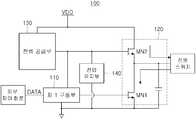
도 1은 본 발명의 전원 스위칭 구동 장치의 개략적인 블럭도이다.1 is a schematic block diagram of a power switching driving apparatus of the present invention.
도 1을 참조하면, 본 발명의 전원 스위칭 구동 장치(100)는 제1 구동부(110), 제2 구동부(120), 전류 공급부(130) 및 전압 유지부(140)를 포함할 수 있다.Referring to FIG. 1, the power
제1 구동부(110)는 외부로부터의 제어 신호(Data)에 따라 스위칭 신호를 제공할 수 있고, 제2 구동부(120)는 사전에 설정된 동작 전원(VDD)을 제공하는 동작 전원단과 접지 사이에 캐스코드 연결된 2개의 N MOS FET(MN1,MN2)를 포함하고, 제1 구동부(110)로부터의 스위칭 신호에 따라 스위칭하여 전원 스위칭을 제어하는 스위칭 제어 신호를 제공할 수 있다.The
전류 공급부(130)는 제2 구동부(120)의 스위칭 제어 신호 제공에 필요한 전류를 공급하고, 전압 유지부(140)는 제2 구동부(120)의 제2 N MOS FET(MN2)의 게이트에 필요한 전압 레벨을 유지할 수 있다.
The
도 2는 본 발명의 전원 스위칭 구동 장치의 보다 상세한 회로도이다.2 is a more detailed circuit diagram of the power switching driving apparatus of the present invention.
도 1과 함께 도 2를 참조하면, 본 발명의 전원 스위칭 구동 장치(100)의 제1 구동부(110)은 적어도 하나의 스위칭 N MOS FET(S)를 포함할 수 있다.Referring to FIG. 1 along with FIG. 1, the
스위칭 N MOS FET(S)의 게이트로는 외부로부터의 제어신호(Data)가 입력되고 드레인은 제2 구동부(120)의 제2 N MOS FET(MN2)의 게이트에 연결될 수 있으며, 소스는 접지에 연결될 수 있다.
The control signal Data from the outside is input to the gate of the switching N MOS FET (S) and the drain may be connected to the gate of the second N MOS FET MN2 of the
제2 구동부(120)의 제1 및 제2 N MOS FET(MN1, MN2)는 상기 동작 전원단과 접지 사이에 캐스코드 연결될 수 있으며, 보다 상세하게는 제1 N MOS FET(MN1)의 게이트는 스위칭 N MOS FET(S)의 게이트와 같이 외부로부터의 제어신호(Data)가 입력되고, 소스는 접지에 연결될 수 있으며, 드레인은 제2 N MOS FET(MN2)의 소스에 연결될 수 있다.The first and second N MOS FETs MN1 and MN2 of the
제2 N MOS FET(MN2)의 게이트는 스위칭 N MOS FET(S)의 드레인 및 전류 공급부(130)에 연결될 수 있고, 드레인은 상기 동작 전원단에 연결될 수 있다.The gate of the second N MOS FET MN2 may be connected to the drain and the
상술한 전기적 연결에 따라 제어 신호(DATA)가 하이 레벨 신호이면 스위칭 N MOS FET(S)와 제1 N MOS FET(MN1)이 스위칭 온 하고, 제2 N MOS FET(MN2)는 스위칭 오프하여 스위칭 소자에 인가되는 전원은 접지로 바이패스된다. 따라서, 스위칭 소자에 전달되는 스위칭 제어 신호는 로우 레벨 신호가 되어 스위칭 소자는 스위칭 오프될 수 있다.According to the electrical connection described above, when the control signal DATA is a high level signal, the switching N MOS FET S and the first N MOS FET MN1 are switched on, and the second N MOS FET MN2 is switched off and switched. Power applied to the device is bypassed to ground. Therefore, the switching control signal transmitted to the switching element becomes a low level signal so that the switching element can be switched off.
제어 신호(DATA)가 로우 레벨 신호이면 스위칭 N MOS FET(S)와 제1 N MOS FET(MN1)이 스위칭 오프하고, 제2 N MOS FET(MN2)는 스위칭 온하여 스위칭 소자에 인가되는 사전에 설정된 레벨의 전원이 인가될 수 있다. 따라서, 스위칭 소자에 전달되는 스위칭 제어 신호는 하이 레벨 신호가 되어 스위칭 소자는 스위칭 온될 수 있다. 이를 위해, 전압 유지부(140)는 제2 N MOS FET(MN2)에 인가되는 전압 레벨을 유지할 수 있다.
When the control signal DATA is a low level signal, the switching N MOS FET S and the first N MOS FET MN1 are switched off, and the second N MOS FET MN2 is switched on to be applied to the switching element in advance. Power of a set level may be applied. Thus, the switching control signal transmitted to the switching element becomes a high level signal so that the switching element can be switched on. To this end, the
전압 유지부(140)는 적어도 하나의 제너 다이오드를 포함할 수 있고, 유지하고자 하는 전압 레벨에 따라 복수의 제너 다이오드(D1~DN)를 포함할 수도 있다. 전압 유지부(140)는 제2 N MOS FET(MN2)의 게이트에 인가되는 전압을 유지하여 제2 N MOS FET(MN2)가 스위칭 온 동작을 수행할 수 있다. 즉, 제2 N MOS FET(MN2)의 게이트-소스간 전압은 일정하게 유지되어 드레인 전류의 변화는 감소할 수 있다. 스위칭 소자에 인가되는 스위칭 제어 신호가 하이 레벨일때 전원 전압에 상관없이 전압 레벨이 일정하게 유지되어 스위칭 소자의 드레인 전류 또한 일정하게 유지될 수 있다. 더하여, 동일한 드레인 전류에 대하여 N MOS FET은 P MOS FET에 비해 회로 면적을 저감할 수 있다. 전압 유지부(140)의 전압을 유지하기 위해 전류 공급부(130)가 채용된다.
The
전류 공급부(130)는 전류원(I)과 캐스코드 연결된 제1 및 제4 P MOS FET로 이루어진 전류 미러부를 포함할 수 있다.The
전류원(I)는 사전에 설정된 레벨의 전류를 공급할 수 있고, 상기 전류 미러부는 전류원(I)으로부터의 전류를 미러링하여 제2 N MOS FET(MN2)의 게이트에 전달할 수 있다.The current source I may supply a current of a predetermined level, and the current mirror unit may mirror the current from the current source I and transfer it to the gate of the second N MOS FET MN2.
이를 위해, 상기 전류 미러부의 상기 동작 전원단과 전류원(I) 사이에 제1 및 제2 P MOS FET(M1,M2)는 캐스코드 연결되고, 상기 동작 전원단과 전압 유지부(140)의 사이에 제3 및 제4 P MOS FET(M3,M4)는 캐스코드 연결될 수 있다. 전류 미러링을 위해 캐스코드 연결된 제1 및 제2 P MOS FET(M1,M2)와 제3 및 제4 P MOS FET(M3,M4)는 병렬 연결될 수 있고, 제1 P MOS FET(M1)의 게이트와 제3 P MOS FET(M3)의 게이트 끼리 연결되고, 제2 P MOS FET(M2)의 게이트와 제4 P MOS FET(M4)의 게이트 끼리 연결될 수 있으며, 제1 P MOS FET(M1)의 게이트와 드레인은 서로 연결되고, 제2 P MOS FET(M2)의 게이트와 드레인은 서로 연결될 수 있다.To this end, first and second P MOS FETs M1 and M2 are cascoded between the operating power supply terminal and the current source I of the current mirror unit, and between the operating power supply terminal and the
전류원(I)의 전류 공급에 의해 전압 유지부(140)의 제너 다이오드는 제너 전압이 생성될 수 있다. 즉, 제너 다이오드는 역방향 전류가 존재하지 않으면 '0' 전압을 유지하다 일전 전류 이상의 전류가 흐르게 되면 전압이 상승하여 제너 전압을 발생시키게 된다. 따라서, 스위칭 제어 신호의 라이징 시간은 제너 전압의 라이징 시간에 비례하게 되며, 상기 전류 미러부의 캐스코드 연결에 의해 전류원(I)의 내부 저항이 향상되어 제너 전압의 라이징 시간을 제어할 수 있다.
The zener diode of the
도 3은 본 발명의 전원 스위칭 구동 장치를 채용한 역률 보정 장치의 개략적인 회로도이다.3 is a schematic circuit diagram of a power factor correcting apparatus employing the power switching driving apparatus of the present invention.
도 3을 참조하면, 본 발명의 전원 스위칭 구동 장치(100)는 역률 보정 장치에 채용될 수 있다.Referring to FIG. 3, the power
즉, 상기 역률 보정 장치는 전원 스위칭 구동 장치(100)와 역률 보정부(200)를 포함할 수 있으며, 역률 보정부(200)는 교류 전원을 정류하는 브리지 다이오드로부터의 정류된 전원을 스위칭하여 전압과 전류간의 위상차를 조정하여 역률을 보정할 수 있으며, 이를 위해, 인덕터(L), 스위칭 소자(S1), 다이오드(D) 및 캐패시터(C1)를 포함할 수 있다.That is, the power factor correcting apparatus may include a power
전원 스위칭 구동 장치(100)는 스위칭 소자(S1)의 스위칭 온 및 오프를 제어하는 스위칭 제어 신호를 제공할 수 있다.The power
전원 스위칭 구동 장치(100)의 세부 구성 및 동작은 상술한 도 1 및 도 2의 설명과 동일하므로 생략하도록 한다.
The detailed configuration and operation of the power
도 4는 본 발명의 전원 스위칭 구동 장치를 채용한 전원 공급 장치의 개략적인 회로도이다.4 is a schematic circuit diagram of a power supply device employing the power switching driving device of the present invention.
도 4를 참조하면, 본 발명의 전원 스위칭 구동 장치(100)는 전원 공급 장치에 채용될 수 있다.Referring to FIG. 4, the power
즉, 상기 전원 공급 장치는 전원 스위칭 구동 장치(100)와 전원 변환부(300)를 포함할 수 있으며, 더하여 역률 보정부(200)를 포함할 수 있다.That is, the power supply device may include a power
전원 변환부(300)은 입력된 전원을 스위칭하고 트랜스포머의 권선비에 따라 전압 레벨을 변환하여 사전에 설정된 직류 전원을 공급할 수 있다. 이를 위해, 전원 변환부(300)는 스위칭 소자(S2), 트랜스포머(T), 다이오드(D) 및 캐패시터(C)를 포함할 수 있다.The
전원 스위칭 구동 장치(100)는 스위칭 소자(S1)의 스위칭 온 및 오프를 제어하는 스위칭 제어 신호를 제공할 수 있다.The power
전원 스위칭 구동 장치(100)의 세부 구성 및 동작은 상술한 도 1 및 도 2의 설명과 동일하므로 생략하도록 한다. 더하여, 역률 보정부(200)는 도 3에 도시된 설명과 동일 또는 유사할 수 있으므로 생략하도록 한다.
The detailed configuration and operation of the power
도 5는 본 발명의 전원 스위칭 구동 장치의 제어 신호 및 스위칭 제어 신호의 시뮬레이션 파형 그래프이다.5 is a simulation waveform graph of a control signal and a switching control signal of the power switching driving apparatus of the present invention.
도 5를 참조하면, 입력된 제어 신호(DATA)의 하이 레벨 및 로우 레벨에 상보적으로 스위칭 제어 신호의 하이 레벨 및 로우 레벨이 형성되는 것을 볼 수 있으며, 제너 다이오드의 라이징 시간에 의해 라이징 및 폴링 시간이 각각 50ns 및 35ns인 것을 볼 수 있다.
Referring to FIG. 5, it can be seen that the high level and the low level of the switching control signal are formed complementarily to the high level and the low level of the input control signal DATA, and the rising and falling by the rising time of the zener diode You can see that the time is 50ns and 35ns respectively.
도 6은 본 발명의 전원 스위칭 구동 장치의 동작 전원(VDD) 전압 변화에 의한 스위칭 제어 신호의 시뮬레이션 파형 그래프이다.6 is a simulation waveform graph of a switching control signal caused by a change in operating power supply voltage VDD of the power switching driving apparatus of the present invention.
도 6을 참조하면, 본 발명의 전원 스위칭 구동 장치의 동작 전원(VDD)의 전압 레벨을 15V에서 25V로 변동하여도 스위칭 제어 신호의 전압 레벨은 일정한 것으로 볼 수 있다. 이에 따라, 스위칭 소자의 게이트-소스간 전압이 일정하게 되어 일정한 드레인 전류를 생성하게 되고, 역류 보정 장치 또는 전원 공급 장치에 채용된 인덕터에 흐르는 전류를 안정적으로 유지시킬 수 있다.
Referring to FIG. 6, even when the voltage level of the operating power supply VDD of the power switching driving apparatus of the present invention is changed from 15V to 25V, the voltage level of the switching control signal may be regarded as constant. Accordingly, the gate-source voltage of the switching element becomes constant to generate a constant drain current, and it is possible to stably maintain the current flowing through the inductor employed in the backflow correction device or the power supply device.
상술한 바와 같이, 본 발명에 따르면, 2개의 NMOS 트랜지스터를 캐스코드 형태로 연결하여 전원 스위칭을 제어함으로써 회로 면적이 저감되고 구동 속도가 빠르며, 동작 전원(VDD)의 전압 레벨이 변동하여도 안정적인 스위칭 제어 신호를 제공할 수 있다.
As described above, according to the present invention, by connecting two NMOS transistors in the form of cascode to control power switching, the circuit area is reduced, the driving speed is high, and the switching is stable even when the voltage level of the operating power supply VDD varies. A control signal can be provided.
이상에서 설명한 본 발명은 전술한 실시예 및 첨부된 도면에 의해 한정되는 것이 아니고 후술하는 특허청구범위에 의해 한정되며, 본 발명의 구성은 본 발명의 기술적 사상을 벗어나지 않는 범위 내에서 그 구성을 다양하게 변경 및 개조할 수 있다는 것을 본 발명이 속하는 기술 분야에서 통상의 지식을 가진 자는 쉽게 알 수 있다.It is to be understood that both the foregoing general description and the following detailed description are exemplary and explanatory and are not intended to limit the invention to the particular forms disclosed. It will be understood by those skilled in the art that various changes in form and details may be made therein without departing from the spirit and scope of the invention as defined by the appended claims.
100...전원 스위칭 구동 장치
110...제1 구동부
120...제2 구동부
130...전류 공급부
140...전압 유지부
200...역률 보정부
300...전원 변환부100 ... power switching drive
110.First drive part
120.2nd drive part
130 ... current supply
140 ... voltage holding part
200 ... Power Factor Correction
300 ... power converter
Claims (21)
Translated fromKorean사전에 설정된 동작 전원을 공급하는 동작 전원단과 접지 사이에 캐스코드 연결된 제1 NMOS FET 및 제2 NMOS FET를 구비하여, 상기 스위칭 신호에 따라 상보적으로 스위칭하여 전원 스위칭을 제어하는 스위칭 제어 신호를 제공하는 제2 구동부;
상기 제2 구동부의 구동에 필요한 전류를 공급하는 전류 공급부; 및
상기 제2 구동부의 구동에 필요한 전압을 유지하는 전압 유지부
를 포함하는 전원 스위칭 구동 장치.
A first driver configured to provide a switching signal according to a control signal from the outside;
A first NMOS FET and a second NMOS FET cascoded between an operating power supply stage for supplying a predetermined operating power supply and a ground are provided to provide a switching control signal for controlling power switching by switching complementarily according to the switching signal. A second drive unit;
A current supply unit supplying a current required to drive the second driver; And
Voltage holding unit for holding a voltage required for driving the second drive unit
Power switching driving device comprising a.
상기 제1 구동부는 상기 제어 신호에 따라 스위칭하는 스위칭 소자를 포함하는 전원 스위칭 구동 장치.
The method of claim 1,
The first driving unit includes a switching element for switching in accordance with the control signal.
상기 제2 N MOS FET는 상기 스위칭 소자의 스위칭 온 및 오프에 따라 스위칭 온 및 오프하고,
상기 제1 N MOS FET는 상기 제2 N MOS FET와 상보적으로 스위칭 온 및 오프하여 상기 스위칭 제어 신호를 제공하는 전원 스위칭 구동 장치.
The method of claim 2,
The second N MOS FET is switched on and off in accordance with the switching on and off of the switching element,
And the first N MOS FET switches on and off complementary to the second N MOS FET to provide the switching control signal.
사전에 설정된 전류를 공급하는 전류원;
상기 동작 전원단과 상기 전류원 사이에 캐스코드 연결된 제1 및 제2 P MOS FET와, 상기 제1 및 제2 P MOS FET와 병렬 연결되고 상기 동작 전원단과 제2 N MOS FET 사이에 캐스코드 연결된 제3 및 제4 P MOS FET를 구비하여 상기 전류원으로부터의 전류를 상기 제2 N MOS FET에 미러링하는 전류 미러링부
를 포함하는 전원 스위칭 구동 장치.
The method of claim 3, wherein the current supply unit
A current source for supplying a preset current;
First and second P MOS FETs cascoded between the operating power source and the current source, and a third cascode connected between the first and second P MOS FETs and cascoded between the operating power source and the second N MOS FET And a fourth P MOS FET to mirror current from the current source to the second N MOS FET.
Power switching driving device comprising a.
상기 전압 유지부는 상기 제2 N MOS FET의 게이트와 접지 사이에 연결된 적어도 하나의 제너 다이오드를 포함하는 전원 스위칭 구동 장치.
5. The method of claim 4,
And the voltage maintaining part includes at least one zener diode connected between the gate and the ground of the second N MOS FET.
상기 스위칭 소자는 스위칭 N MOS FET인 전원 스위칭 구동 장치.
The method of claim 2,
And said switching element is a switching N MOS FET.
외부로부터의 제어 신호에 따라 스위칭 신호를 제공하는 제1 구동부와, 사전에 설정된 동작 전원을 공급하는 동작 전원단과 접지 사이에 캐스코드 연결되어 상기 스위칭 신호에 따라 상보적으로 스위칭하여 상기 스위칭 제어 신호를 제공하는 제1 NMOS FET 및 제2 NMOS FET를 구비하는 제2 구동부를 갖는 전원 스위칭 구동 장치
를 포함하는 역률 보정 장치.
A power factor correction unit configured to correct the power factor by switching the rectified power according to the switching control signal; And
A cascode connection is provided between a first driver for providing a switching signal according to a control signal from an external source, an operation power supply terminal for supplying a predetermined operating power, and ground to switch complementarily according to the switching signal to thereby switch the switching control signal. A power supply switching driving apparatus having a second driver having a first NMOS FET and a second NMOS FET to provide.
Lt; / RTI >
상기 제2 구동부의 구동에 필요한 전류를 공급하는 전류 공급부; 및
상기 제2 구동부의 구동에 필요한 전압을 유지하는 전압 유지부
를 더 포함하는 역률 보정 장치.
The method of claim 7, wherein the power switching driving device
A current supply unit supplying a current required to drive the second driver; And
Voltage holding unit for holding a voltage required for driving the second drive unit
Power factor correction device further comprising.
상기 제1 구동부는 상기 제어 신호에 따라 스위칭하는 스위칭 소자를 포함하는 역률 보정 장치.
9. The method of claim 8,
The power factor correction apparatus of claim 1, wherein the first driving unit comprises a switching element that switches according to the control signal.
상기 제2 N MOS FET는 상기 스위칭 소자의 스위칭 온 및 오프에 따라 스위칭 온 및 오프하고,
상기 제1 N MOS FET는 상기 제2 N MOS FET와 상보적으로 스위칭 온 및 오프하여 상기 스위칭 제어 신호를 제공하는 역률 보정 장치.
10. The method of claim 9,
The second N MOS FET is switched on and off in accordance with the switching on and off of the switching element,
And the first N MOS FET switches on and off complementarily with the second N MOS FET to provide the switching control signal.
사전에 설정된 전류를 공급하는 전류원;
상기 동작 전원단과 상기 전류원 사이에 캐스코드 연결된 제1 및 제2 P MOS FET와, 상기 제1 및 제2 P MOS FET와 병렬 연결되고 상기 동작 전원단과 제2 N MOS FET 사이에 캐스코드 연결된 제3 및 제4 P MOS FET를 구비하여 상기 전류원으로부터의 전류를 상기 제2 N MOS FET에 미러링하는 전류 미러링부
를 포함하는 역률 보정 장치.
The method of claim 10, wherein the current supply unit
A current source for supplying a preset current;
First and second P MOS FETs cascoded between the operating power source and the current source, and a third cascode connected between the first and second P MOS FETs and cascoded between the operating power source and the second N MOS FET And a fourth P MOS FET to mirror current from the current source to the second N MOS FET.
Lt; / RTI >
상기 전압 유지부는 상기 제2 N MOS FET의 게이트와 접지 사이에 연결된 적어도 하나의 제너 다이오드를 포함하는 역률 보정 장치.
The method of claim 11,
And the voltage maintaining unit includes at least one zener diode connected between the gate and the ground of the second N MOS FET.
상기 스위칭 소자는 스위칭 N MOS FET인 역률 보정 장치.
10. The method of claim 9,
And the switching element is a switching N MOS FET.
외부로부터의 제어 신호에 따라 스위칭 신호를 제공하는 제1 구동부와, 사전에 설정된 동작 전원을 공급하는 동작 전원단과 접지 사이에 캐스코드 연결되어 상기 스위칭 신호에 따라 상보적으로 스위칭하여 상기 스위칭 제어 신호를 제공하는 제1 NMOS FET 및 제2 NMOS FET를 구비하는 제2 구동부를 갖는 전원 스위칭 구동 장치
를 포함하는 전원 공급 장치.
A power converter configured to output input driving power by switching input power according to a switching control signal; And
A cascode connection is provided between a first driver for providing a switching signal according to a control signal from an external source, an operation power supply terminal for supplying a predetermined operating power, and ground to switch complementarily according to the switching signal to thereby switch the switching control signal. A power supply switching driving apparatus having a second driver having a first NMOS FET and a second NMOS FET to provide.
Power supply comprising a.
상기 제2 구동부의 구동에 필요한 전류를 공급하는 전류 공급부; 및
상기 제2 구동부의 구동에 필요한 전압을 유지하는 전압 유지부
를 더 포함하는 전원 공급 장치.
15. The apparatus of claim 14, wherein the power switching driving device
A current supply unit supplying a current required to drive the second driver; And
Voltage holding unit for holding a voltage required for driving the second drive unit
Further comprising a power supply.
상기 제1 구동부는 상기 제어 신호에 따라 스위칭하는 스위칭 소자를 포함하는 전원 공급 장치.
16. The method of claim 15,
The first driving unit includes a switching element for switching in accordance with the control signal.
상기 제2 N MOS FET는 상기 스위칭 소자의 스위칭 온 및 오프에 따라 스위칭 온 및 오프하고,
상기 제1 N MOS FET는 상기 제2 N MOS FET와 상보적으로 스위칭 온 및 오프하여 상기 스위칭 제어 신호를 제공하는 전원 공급 장치.
17. The method of claim 16,
The second N MOS FET is switched on and off in accordance with the switching on and off of the switching element,
And the first N MOS FET switches on and off complementarily with the second N MOS FET to provide the switching control signal.
사전에 설정된 전류를 공급하는 전류원;
상기 동작 전원단과 상기 전류원 사이에 캐스코드 연결된 제1 및 제2 P MOS FET와, 상기 제1 및 제2 P MOS FET와 병렬 연결되고 상기 동작 전원단과 제2 N MOS FET 사이에 캐스코드 연결된 제3 및 제4 P MOS FET를 구비하여 상기 전류원으로부터의 전류를 상기 제2 N MOS FET에 미러링하는 전류 미러링부
를 포함하는 전원 공급 장치.
The method of claim 17, wherein the current supply unit
A current source for supplying a preset current;
First and second P MOS FETs cascoded between the operating power source and the current source, and a third cascode connected between the first and second P MOS FETs and cascoded between the operating power source and the second N MOS FET And a fourth P MOS FET to mirror current from the current source to the second N MOS FET.
Power supply comprising a.
상기 전압 유지부는 상기 제2 N MOS FET의 게이트와 접지 사이에 연결된 적어도 하나의 제너 다이오드를 포함하는 전원 공급 장치.
19. The method of claim 18,
The voltage supply unit includes at least one zener diode connected between the gate and the ground of the second N MOS FET.
정류된 전원을 스위칭하여 역률 보정한 후 상기 전원 변환부에 제공하는 역률 보정부를 더 포함하는 전원 공급 장치.
15. The method of claim 14,
And a power factor correction unit for switching the rectified power to correct the power factor and providing the power factor to the power converter.
상기 스위칭 소자는 스위칭 N MOS FET인 전원 공급 장치.17. The method of claim 16,
The switching device is a switching N MOS FET.
Priority Applications (2)
| Application Number | Priority Date | Filing Date | Title |
|---|---|---|---|
| KR1020110141634AKR20130073669A (en) | 2011-12-23 | 2011-12-23 | Driving apparatus for power switching and power factor correction apparatus having theeof and power supply having thereof |
| US13/405,791US20130163289A1 (en) | 2011-12-23 | 2012-02-27 | Power switching driving apparatus, and power factor correction device and power supply device having the same |
Applications Claiming Priority (1)
| Application Number | Priority Date | Filing Date | Title |
|---|---|---|---|
| KR1020110141634AKR20130073669A (en) | 2011-12-23 | 2011-12-23 | Driving apparatus for power switching and power factor correction apparatus having theeof and power supply having thereof |
Publications (1)
| Publication Number | Publication Date |
|---|---|
| KR20130073669Atrue KR20130073669A (en) | 2013-07-03 |
Family
ID=48654370
Family Applications (1)
| Application Number | Title | Priority Date | Filing Date |
|---|---|---|---|
| KR1020110141634AWithdrawnKR20130073669A (en) | 2011-12-23 | 2011-12-23 | Driving apparatus for power switching and power factor correction apparatus having theeof and power supply having thereof |
Country Status (2)
| Country | Link |
|---|---|
| US (1) | US20130163289A1 (en) |
| KR (1) | KR20130073669A (en) |
Cited By (4)
| Publication number | Priority date | Publication date | Assignee | Title |
|---|---|---|---|---|
| KR20160150302A (en)* | 2015-06-22 | 2016-12-30 | 강희복 | A power supply circuit system using a negative threshold five-terminal NMOS FET device with multiple step connection for power RF |
| KR101694100B1 (en)* | 2016-05-25 | 2017-01-17 | 강희복 | A power supply circuit system using a negative threshold five-terminal NMOS FET device for full-wave rectifier using case-embedded antenna |
| KR20170092091A (en)* | 2016-02-02 | 2017-08-10 | 삼성전자주식회사 | Polymorphic storage devices |
| US20230095863A1 (en)* | 2021-09-24 | 2023-03-30 | Kabushiki Kaisha Toshiba | Power supply circuit |
Families Citing this family (73)
| Publication number | Priority date | Publication date | Assignee | Title |
|---|---|---|---|---|
| US8326814B2 (en) | 2007-12-05 | 2012-12-04 | Box, Inc. | Web-based file management system and service |
| WO2012099617A1 (en) | 2011-01-20 | 2012-07-26 | Box.Net, Inc. | Real time notification of activities that occur in a web-based collaboration environment |
| US9015601B2 (en) | 2011-06-21 | 2015-04-21 | Box, Inc. | Batch uploading of content to a web-based collaboration environment |
| US9063912B2 (en) | 2011-06-22 | 2015-06-23 | Box, Inc. | Multimedia content preview rendering in a cloud content management system |
| US9652741B2 (en) | 2011-07-08 | 2017-05-16 | Box, Inc. | Desktop application for access and interaction with workspaces in a cloud-based content management system and synchronization mechanisms thereof |
| GB2503625A (en) | 2011-07-08 | 2014-01-01 | Box Inc | Collaboration sessions in a workspace on cloud-based content management system |
| US9197718B2 (en) | 2011-09-23 | 2015-11-24 | Box, Inc. | Central management and control of user-contributed content in a web-based collaboration environment and management console thereof |
| US8515902B2 (en) | 2011-10-14 | 2013-08-20 | Box, Inc. | Automatic and semi-automatic tagging features of work items in a shared workspace for metadata tracking in a cloud-based content management system with selective or optional user contribution |
| US9098474B2 (en) | 2011-10-26 | 2015-08-04 | Box, Inc. | Preview pre-generation based on heuristics and algorithmic prediction/assessment of predicted user behavior for enhancement of user experience |
| US11210610B2 (en) | 2011-10-26 | 2021-12-28 | Box, Inc. | Enhanced multimedia content preview rendering in a cloud content management system |
| US8990307B2 (en) | 2011-11-16 | 2015-03-24 | Box, Inc. | Resource effective incremental updating of a remote client with events which occurred via a cloud-enabled platform |
| GB2500152A (en) | 2011-11-29 | 2013-09-11 | Box Inc | Mobile platform file and folder selection functionalities for offline access and synchronization |
| US9019123B2 (en) | 2011-12-22 | 2015-04-28 | Box, Inc. | Health check services for web-based collaboration environments |
| US9904435B2 (en) | 2012-01-06 | 2018-02-27 | Box, Inc. | System and method for actionable event generation for task delegation and management via a discussion forum in a web-based collaboration environment |
| US11232481B2 (en) | 2012-01-30 | 2022-01-25 | Box, Inc. | Extended applications of multimedia content previews in the cloud-based content management system |
| US9965745B2 (en) | 2012-02-24 | 2018-05-08 | Box, Inc. | System and method for promoting enterprise adoption of a web-based collaboration environment |
| US9195636B2 (en) | 2012-03-07 | 2015-11-24 | Box, Inc. | Universal file type preview for mobile devices |
| US9064722B2 (en)* | 2012-03-13 | 2015-06-23 | International Business Machines Corporation | Breakdown voltage multiplying integration scheme |
| US9054919B2 (en) | 2012-04-05 | 2015-06-09 | Box, Inc. | Device pinning capability for enterprise cloud service and storage accounts |
| US9575981B2 (en) | 2012-04-11 | 2017-02-21 | Box, Inc. | Cloud service enabled to handle a set of files depicted to a user as a single file in a native operating system |
| US9413587B2 (en) | 2012-05-02 | 2016-08-09 | Box, Inc. | System and method for a third-party application to access content within a cloud-based platform |
| US9396216B2 (en) | 2012-05-04 | 2016-07-19 | Box, Inc. | Repository redundancy implementation of a system which incrementally updates clients with events that occurred via a cloud-enabled platform |
| US9691051B2 (en) | 2012-05-21 | 2017-06-27 | Box, Inc. | Security enhancement through application access control |
| US9027108B2 (en) | 2012-05-23 | 2015-05-05 | Box, Inc. | Systems and methods for secure file portability between mobile applications on a mobile device |
| US8914900B2 (en) | 2012-05-23 | 2014-12-16 | Box, Inc. | Methods, architectures and security mechanisms for a third-party application to access content in a cloud-based platform |
| US9021099B2 (en) | 2012-07-03 | 2015-04-28 | Box, Inc. | Load balancing secure FTP connections among multiple FTP servers |
| GB2505072A (en) | 2012-07-06 | 2014-02-19 | Box Inc | Identifying users and collaborators as search results in a cloud-based system |
| US9712510B2 (en) | 2012-07-06 | 2017-07-18 | Box, Inc. | Systems and methods for securely submitting comments among users via external messaging applications in a cloud-based platform |
| US9792320B2 (en) | 2012-07-06 | 2017-10-17 | Box, Inc. | System and method for performing shard migration to support functions of a cloud-based service |
| US9473532B2 (en) | 2012-07-19 | 2016-10-18 | Box, Inc. | Data loss prevention (DLP) methods by a cloud service including third party integration architectures |
| US9794256B2 (en) | 2012-07-30 | 2017-10-17 | Box, Inc. | System and method for advanced control tools for administrators in a cloud-based service |
| US9369520B2 (en) | 2012-08-19 | 2016-06-14 | Box, Inc. | Enhancement of upload and/or download performance based on client and/or server feedback information |
| US8745267B2 (en) | 2012-08-19 | 2014-06-03 | Box, Inc. | Enhancement of upload and/or download performance based on client and/or server feedback information |
| US9558202B2 (en) | 2012-08-27 | 2017-01-31 | Box, Inc. | Server side techniques for reducing database workload in implementing selective subfolder synchronization in a cloud-based environment |
| US9135462B2 (en) | 2012-08-29 | 2015-09-15 | Box, Inc. | Upload and download streaming encryption to/from a cloud-based platform |
| US9117087B2 (en) | 2012-09-06 | 2015-08-25 | Box, Inc. | System and method for creating a secure channel for inter-application communication based on intents |
| US9195519B2 (en) | 2012-09-06 | 2015-11-24 | Box, Inc. | Disabling the self-referential appearance of a mobile application in an intent via a background registration |
| US9311071B2 (en) | 2012-09-06 | 2016-04-12 | Box, Inc. | Force upgrade of a mobile application via a server side configuration file |
| US9292833B2 (en) | 2012-09-14 | 2016-03-22 | Box, Inc. | Batching notifications of activities that occur in a web-based collaboration environment |
| US10200256B2 (en) | 2012-09-17 | 2019-02-05 | Box, Inc. | System and method of a manipulative handle in an interactive mobile user interface |
| US9553758B2 (en) | 2012-09-18 | 2017-01-24 | Box, Inc. | Sandboxing individual applications to specific user folders in a cloud-based service |
| US10915492B2 (en) | 2012-09-19 | 2021-02-09 | Box, Inc. | Cloud-based platform enabled with media content indexed for text-based searches and/or metadata extraction |
| US9959420B2 (en) | 2012-10-02 | 2018-05-01 | Box, Inc. | System and method for enhanced security and management mechanisms for enterprise administrators in a cloud-based environment |
| US9705967B2 (en) | 2012-10-04 | 2017-07-11 | Box, Inc. | Corporate user discovery and identification of recommended collaborators in a cloud platform |
| US9495364B2 (en) | 2012-10-04 | 2016-11-15 | Box, Inc. | Enhanced quick search features, low-barrier commenting/interactive features in a collaboration platform |
| US9665349B2 (en) | 2012-10-05 | 2017-05-30 | Box, Inc. | System and method for generating embeddable widgets which enable access to a cloud-based collaboration platform |
| US9756022B2 (en) | 2014-08-29 | 2017-09-05 | Box, Inc. | Enhanced remote key management for an enterprise in a cloud-based environment |
| GB2507191B (en) | 2012-10-17 | 2015-03-04 | Box Inc | Remote key management in a cloud-based environment |
| US10235383B2 (en) | 2012-12-19 | 2019-03-19 | Box, Inc. | Method and apparatus for synchronization of items with read-only permissions in a cloud-based environment |
| US9396245B2 (en) | 2013-01-02 | 2016-07-19 | Box, Inc. | Race condition handling in a system which incrementally updates clients with events that occurred in a cloud-based collaboration platform |
| US9953036B2 (en) | 2013-01-09 | 2018-04-24 | Box, Inc. | File system monitoring in a system which incrementally updates clients with events that occurred in a cloud-based collaboration platform |
| EP2755151A3 (en) | 2013-01-11 | 2014-09-24 | Box, Inc. | Functionalities, features and user interface of a synchronization client to a cloud-based environment |
| US10599671B2 (en) | 2013-01-17 | 2020-03-24 | Box, Inc. | Conflict resolution, retry condition management, and handling of problem files for the synchronization client to a cloud-based platform |
| US10725968B2 (en) | 2013-05-10 | 2020-07-28 | Box, Inc. | Top down delete or unsynchronization on delete of and depiction of item synchronization with a synchronization client to a cloud-based platform |
| US10846074B2 (en) | 2013-05-10 | 2020-11-24 | Box, Inc. | Identification and handling of items to be ignored for synchronization with a cloud-based platform by a synchronization client |
| US9633037B2 (en) | 2013-06-13 | 2017-04-25 | Box, Inc | Systems and methods for synchronization event building and/or collapsing by a synchronization component of a cloud-based platform |
| US9805050B2 (en) | 2013-06-21 | 2017-10-31 | Box, Inc. | Maintaining and updating file system shadows on a local device by a synchronization client of a cloud-based platform |
| US10229134B2 (en) | 2013-06-25 | 2019-03-12 | Box, Inc. | Systems and methods for managing upgrades, migration of user data and improving performance of a cloud-based platform |
| US10110656B2 (en) | 2013-06-25 | 2018-10-23 | Box, Inc. | Systems and methods for providing shell communication in a cloud-based platform |
| US9535924B2 (en) | 2013-07-30 | 2017-01-03 | Box, Inc. | Scalability improvement in a system which incrementally updates clients with events that occurred in a cloud-based collaboration platform |
| US9704137B2 (en) | 2013-09-13 | 2017-07-11 | Box, Inc. | Simultaneous editing/accessing of content by collaborator invitation through a web-based or mobile application to a cloud-based collaboration platform |
| GB2518298A (en) | 2013-09-13 | 2015-03-18 | Box Inc | High-availability architecture for a cloud-based concurrent-access collaboration platform |
| US8892679B1 (en) | 2013-09-13 | 2014-11-18 | Box, Inc. | Mobile device, methods and user interfaces thereof in a mobile device platform featuring multifunctional access and engagement in a collaborative environment provided by a cloud-based platform |
| US9535909B2 (en) | 2013-09-13 | 2017-01-03 | Box, Inc. | Configurable event-based automation architecture for cloud-based collaboration platforms |
| US10509527B2 (en) | 2013-09-13 | 2019-12-17 | Box, Inc. | Systems and methods for configuring event-based automation in cloud-based collaboration platforms |
| US9213684B2 (en) | 2013-09-13 | 2015-12-15 | Box, Inc. | System and method for rendering document in web browser or mobile device regardless of third-party plug-in software |
| US10866931B2 (en) | 2013-10-22 | 2020-12-15 | Box, Inc. | Desktop application for accessing a cloud collaboration platform |
| US10530854B2 (en) | 2014-05-30 | 2020-01-07 | Box, Inc. | Synchronization of permissioned content in cloud-based environments |
| US9602514B2 (en) | 2014-06-16 | 2017-03-21 | Box, Inc. | Enterprise mobility management and verification of a managed application by a content provider |
| US10574442B2 (en) | 2014-08-29 | 2020-02-25 | Box, Inc. | Enhanced remote key management for an enterprise in a cloud-based environment |
| US9894119B2 (en) | 2014-08-29 | 2018-02-13 | Box, Inc. | Configurable metadata-based automation and content classification architecture for cloud-based collaboration platforms |
| US10038731B2 (en) | 2014-08-29 | 2018-07-31 | Box, Inc. | Managing flow-based interactions with cloud-based shared content |
| US12401358B1 (en)* | 2024-02-15 | 2025-08-26 | Aerojet Rocketdyne, Inc. | Shoot-through protection circuit |
Family Cites Families (10)
| Publication number | Priority date | Publication date | Assignee | Title |
|---|---|---|---|---|
| JP2774176B2 (en)* | 1990-03-20 | 1998-07-09 | 富士通株式会社 | Semiconductor integrated circuit |
| US5825218A (en)* | 1996-10-24 | 1998-10-20 | Stmicroelectronics, Inc. | Driver circuit including slew rate control system with improved voltage ramp generator |
| US6078204A (en)* | 1996-12-19 | 2000-06-20 | Texas Instruments Incorporated | High current drain-to-gate clamp/gate-to-source clamp for external power MOS transistors |
| JP4785271B2 (en)* | 2001-04-27 | 2011-10-05 | 株式会社半導体エネルギー研究所 | Liquid crystal display device, electronic equipment |
| US6617906B1 (en)* | 2002-10-01 | 2003-09-09 | Texas Instruments Incorporated | Low-current compliance stack using nondeterministically biased Zener strings |
| JP3746049B2 (en)* | 2003-09-24 | 2006-02-15 | 株式会社リコー | Laser diode drive circuit |
| JP4774987B2 (en)* | 2005-12-28 | 2011-09-21 | サンケン電気株式会社 | Switching power supply |
| US8330492B2 (en)* | 2006-06-02 | 2012-12-11 | Semiconductor Energy Laboratory Co., Ltd. | Liquid crystal display device and electronic device |
| JP4536108B2 (en)* | 2007-12-12 | 2010-09-01 | Okiセミコンダクタ株式会社 | Load drive circuit |
| US8994439B2 (en)* | 2012-04-19 | 2015-03-31 | Semiconductor Energy Laboratory Co., Ltd. | Semiconductor device, image display device, storage device, and electronic device |
- 2011
- 2011-12-23KRKR1020110141634Apatent/KR20130073669A/ennot_activeWithdrawn
- 2012
- 2012-02-27USUS13/405,791patent/US20130163289A1/ennot_activeAbandoned
Cited By (5)
| Publication number | Priority date | Publication date | Assignee | Title |
|---|---|---|---|---|
| KR20160150302A (en)* | 2015-06-22 | 2016-12-30 | 강희복 | A power supply circuit system using a negative threshold five-terminal NMOS FET device with multiple step connection for power RF |
| KR20170092091A (en)* | 2016-02-02 | 2017-08-10 | 삼성전자주식회사 | Polymorphic storage devices |
| KR101694100B1 (en)* | 2016-05-25 | 2017-01-17 | 강희복 | A power supply circuit system using a negative threshold five-terminal NMOS FET device for full-wave rectifier using case-embedded antenna |
| US20230095863A1 (en)* | 2021-09-24 | 2023-03-30 | Kabushiki Kaisha Toshiba | Power supply circuit |
| US12088199B2 (en)* | 2021-09-24 | 2024-09-10 | Kabushiki Kaisha Toshiba | Power supply circuit |
Also Published As
| Publication number | Publication date |
|---|---|
| US20130163289A1 (en) | 2013-06-27 |
Similar Documents
| Publication | Publication Date | Title |
|---|---|---|
| KR20130073669A (en) | Driving apparatus for power switching and power factor correction apparatus having theeof and power supply having thereof | |
| US9791480B2 (en) | Current sensing of switching power regulators | |
| KR101222793B1 (en) | Mosfet gate drive with reduced power loss | |
| US8866341B2 (en) | Voltage regulator | |
| TWI232021B (en) | Programmable current-sensing circuit providing discrete step temperature compensation for DC-DC converter | |
| CN102200792B (en) | Constant voltage circuit, comparator and voltage supervision circuit equipped therewith | |
| JP2009100602A (en) | Dc-dc converter | |
| ATE459129T1 (en) | SWITCHING POWER SUPPLY SYSTEM AND CONTROL DRIVE WITH SUCH A SYSTEM | |
| US9559668B2 (en) | Drive circuit and semiconductor apparatus | |
| JP2010193431A (en) | Output circuit and motor drive apparatus | |
| TW201330478A (en) | Bridge rectifier for a PFC power converter | |
| US9459639B2 (en) | Power supply circuit with control unit | |
| US11209464B2 (en) | Current detection circuit and power converter | |
| KR20170131452A (en) | Drive for cascode stack of power FETs | |
| CN103365332A (en) | Overcurrent protection circuit and power supply device | |
| CN103631298B (en) | Linear stable | |
| JP5565883B2 (en) | Load balance circuit, power supply device, and load balance control method | |
| TWI580164B (en) | Integrated circuit device with dual mode boost regulator, low power circuit arrangement and high power circuit arrangement comprising the same, and method using the same | |
| CN109194126B (en) | Power supply switching circuit | |
| US9806613B2 (en) | Combined high side and low side current sensing | |
| JP2010282432A (en) | Regulator circuit | |
| JP2010246287A (en) | Current control circuit | |
| CN105474119B (en) | Low headroom constant current source for high current applications | |
| CN201122906Y (en) | Synchronous rectification control circuit | |
| KR101233354B1 (en) | Semiconductor Switch |
Legal Events
| Date | Code | Title | Description |
|---|---|---|---|
| PA0109 | Patent application | Patent event code:PA01091R01D Comment text:Patent Application Patent event date:20111223 | |
| PG1501 | Laying open of application | ||
| PC1203 | Withdrawal of no request for examination | ||
| WITN | Application deemed withdrawn, e.g. because no request for examination was filed or no examination fee was paid |