KR20130070956A - Optical communication module and method of producting optical communication module - Google Patents
Optical communication module and method of producting optical communication moduleDownload PDFInfo
- Publication number
- KR20130070956A KR20130070956AKR1020110138237AKR20110138237AKR20130070956AKR 20130070956 AKR20130070956 AKR 20130070956AKR 1020110138237 AKR1020110138237 AKR 1020110138237AKR 20110138237 AKR20110138237 AKR 20110138237AKR 20130070956 AKR20130070956 AKR 20130070956A
- Authority
- KR
- South Korea
- Prior art keywords
- optical
- optical element
- waveguide
- block
- communication module
- Prior art date
- Legal status (The legal status is an assumption and is not a legal conclusion. Google has not performed a legal analysis and makes no representation as to the accuracy of the status listed.)
- Withdrawn
Links
- 230000003287optical effectEffects0.000titleclaimsabstractdescription325
- 238000004891communicationMethods0.000titleclaimsabstractdescription60
- 238000000034methodMethods0.000titleclaimsdescription19
- 229910052751metalInorganic materials0.000claimsabstractdescription71
- 239000002184metalSubstances0.000claimsabstractdescription71
- 239000004020conductorSubstances0.000claimsdescription22
- 239000000463materialSubstances0.000claimsdescription19
- 239000004593EpoxySubstances0.000claimsdescription15
- 238000004519manufacturing processMethods0.000claimsdescription10
- BQCADISMDOOEFD-UHFFFAOYSA-NSilverChemical compound[Ag]BQCADISMDOOEFD-UHFFFAOYSA-N0.000claimsdescription8
- 229910052709silverInorganic materials0.000claimsdescription8
- 239000004332silverSubstances0.000claimsdescription8
- 239000013307optical fiberSubstances0.000description10
- 229910052710siliconInorganic materials0.000description10
- 239000010703siliconSubstances0.000description10
- XUIMIQQOPSSXEZ-UHFFFAOYSA-NSiliconChemical compound[Si]XUIMIQQOPSSXEZ-UHFFFAOYSA-N0.000description8
- VYPSYNLAJGMNEJ-UHFFFAOYSA-NSilicium dioxideChemical compoundO=[Si]=OVYPSYNLAJGMNEJ-UHFFFAOYSA-N0.000description5
- 239000007769metal materialSubstances0.000description5
- 238000012360testing methodMethods0.000description5
- 239000010949copperSubstances0.000description4
- 230000008569processEffects0.000description4
- 239000000919ceramicSubstances0.000description3
- 230000001427coherent effectEffects0.000description3
- 238000005530etchingMethods0.000description3
- 239000010453quartzSubstances0.000description3
- 229910000679solderInorganic materials0.000description3
- JBRZTFJDHDCESZ-UHFFFAOYSA-NAsGaChemical compound[As]#[Ga]JBRZTFJDHDCESZ-UHFFFAOYSA-N0.000description2
- RYGMFSIKBFXOCR-UHFFFAOYSA-NCopperChemical compound[Cu]RYGMFSIKBFXOCR-UHFFFAOYSA-N0.000description2
- GPXJNWSHGFTCBW-UHFFFAOYSA-NIndium phosphideChemical compound[In]#PGPXJNWSHGFTCBW-UHFFFAOYSA-N0.000description2
- 230000008859changeEffects0.000description2
- 229910052802copperInorganic materials0.000description2
- 230000008878couplingEffects0.000description2
- 238000010168coupling processMethods0.000description2
- 238000005859coupling reactionMethods0.000description2
- 150000003376siliconChemical class0.000description2
- 238000003466weldingMethods0.000description2
- 230000005540biological transmissionEffects0.000description1
- 230000015556catabolic processEffects0.000description1
- 230000007423decreaseEffects0.000description1
- 238000006731degradation reactionMethods0.000description1
- 230000009977dual effectEffects0.000description1
- 238000005516engineering processMethods0.000description1
- 238000012986modificationMethods0.000description1
- 230000004048modificationEffects0.000description1
- 239000000377silicon dioxideSubstances0.000description1
- 238000012546transferMethods0.000description1
Images


Classifications
- G—PHYSICS
- G02—OPTICS
- G02B—OPTICAL ELEMENTS, SYSTEMS OR APPARATUS
- G02B6/00—Light guides; Structural details of arrangements comprising light guides and other optical elements, e.g. couplings
- G02B6/24—Coupling light guides
- G02B6/42—Coupling light guides with opto-electronic elements
- G—PHYSICS
- G02—OPTICS
- G02B—OPTICAL ELEMENTS, SYSTEMS OR APPARATUS
- G02B6/00—Light guides; Structural details of arrangements comprising light guides and other optical elements, e.g. couplings
- G02B6/24—Coupling light guides
- G02B6/42—Coupling light guides with opto-electronic elements
- G02B6/4201—Packages, e.g. shape, construction, internal or external details
- G02B6/4266—Thermal aspects, temperature control or temperature monitoring
- G02B6/4267—Reduction of thermal stress, e.g. by selecting thermal coefficient of materials
- G—PHYSICS
- G02—OPTICS
- G02B—OPTICAL ELEMENTS, SYSTEMS OR APPARATUS
- G02B6/00—Light guides; Structural details of arrangements comprising light guides and other optical elements, e.g. couplings
- G02B6/24—Coupling light guides
- G02B6/42—Coupling light guides with opto-electronic elements
- G02B6/4201—Packages, e.g. shape, construction, internal or external details
- G02B6/4219—Mechanical fixtures for holding or positioning the elements relative to each other in the couplings; Alignment methods for the elements, e.g. measuring or observing methods especially used therefor
- G02B6/4236—Fixing or mounting methods of the aligned elements
- G02B6/4239—Adhesive bonding; Encapsulation with polymer material
- G—PHYSICS
- G02—OPTICS
- G02B—OPTICAL ELEMENTS, SYSTEMS OR APPARATUS
- G02B6/00—Light guides; Structural details of arrangements comprising light guides and other optical elements, e.g. couplings
- G02B6/24—Coupling light guides
- G02B6/42—Coupling light guides with opto-electronic elements
- G02B6/4201—Packages, e.g. shape, construction, internal or external details
- G02B6/4219—Mechanical fixtures for holding or positioning the elements relative to each other in the couplings; Alignment methods for the elements, e.g. measuring or observing methods especially used therefor
- G02B6/4236—Fixing or mounting methods of the aligned elements
- G02B6/4245—Mounting of the opto-electronic elements
- G—PHYSICS
- G02—OPTICS
- G02B—OPTICAL ELEMENTS, SYSTEMS OR APPARATUS
- G02B6/00—Light guides; Structural details of arrangements comprising light guides and other optical elements, e.g. couplings
- G02B6/24—Coupling light guides
- G02B6/42—Coupling light guides with opto-electronic elements
- G02B6/4201—Packages, e.g. shape, construction, internal or external details
- G02B6/4266—Thermal aspects, temperature control or temperature monitoring
- G02B6/4268—Cooling
- G02B6/4272—Cooling with mounting substrates of high thermal conductivity
- Y—GENERAL TAGGING OF NEW TECHNOLOGICAL DEVELOPMENTS; GENERAL TAGGING OF CROSS-SECTIONAL TECHNOLOGIES SPANNING OVER SEVERAL SECTIONS OF THE IPC; TECHNICAL SUBJECTS COVERED BY FORMER USPC CROSS-REFERENCE ART COLLECTIONS [XRACs] AND DIGESTS
- Y10—TECHNICAL SUBJECTS COVERED BY FORMER USPC
- Y10T—TECHNICAL SUBJECTS COVERED BY FORMER US CLASSIFICATION
- Y10T156/00—Adhesive bonding and miscellaneous chemical manufacture
- Y10T156/10—Methods of surface bonding and/or assembly therefor
Landscapes
- Physics & Mathematics (AREA)
- General Physics & Mathematics (AREA)
- Optics & Photonics (AREA)
- Optical Integrated Circuits (AREA)
- Optical Couplings Of Light Guides (AREA)
Abstract
Translated fromKoreanDescription
Translated fromKorean본 발명은 광 통신 모듈 및 광 통신 모듈의 제조 방법에 관한 것이다.The present invention relates to an optical communication module and a method for manufacturing the optical communication module.
광통신 기술이 고도화됨에 따라 새로운 기능을 갖는 광 통신 모듈이 도입되고 있다. 수신기 모듈의 예를 참조하면, 기존의 단일 소자를 이용한 광 수신기는 하나의 광 다이오드를 포함하고, 광 신호의 온 및 오프의 감지에 사용되었다. 반면, 최근에, 한 쌍의 광 다이오드들을 연결해서 두 광 신호들의 차이를 검출하는 밸런스 광수신기, 2쌍 또는 4쌍의 광 다이오드들이 광 하이브리드와 함께 패키징된 광 모듈(예를 들어, 코히어런트(coherent) 광 수신기)와 같은 광 통신 모듈이 개발되고 있다. 이와 같은 광 통신 모듈은 차세대 초고속 대용량 광통신 전송 방식인 이중 편광 직교 위상 변조(DP-QPSK)된 신호나 광 코히어런트 직교 주파수 분할 다중(CO-OFDM) 변조된 신호를 복조하는 데에 사용된다.As optical communication technology is advanced, optical communication modules having new functions are introduced. Referring to the example of the receiver module, the conventional optical receiver using a single element includes a single photodiode and has been used to detect on and off of an optical signal. On the other hand, recently, an optical module (eg, coherent) in which a balanced photoreceiver, two or four pairs of photodiodes, which connect a pair of photodiodes to detect a difference between two optical signals, is packaged together with an optical hybrid. Optical communication modules, such as (coherent) optical receivers, are being developed. The optical communication module is used to demodulate a dual polarized quadrature quadrature phase modulated (DP-QPSK) signal or an optical coherent quadrature frequency division multiplexed (CO-OFDM) modulated signal, which is a next generation high-speed, high-capacity optical fiber transmission method.
광 통신 모듈에서, 광 다이오드들에 광섬유들이 광 결합된다. 광섬유들은 어레이 형태일 수 있고 실리콘 광 벤치(Silicone optical bench, SiOB)에 올려져 고정된 형태일 수 있다. 광섬유 어레이는 광 정렬 후 레이저 용접으로 광 통신 모듈에 고정된다. 실리콘 광 벤치(SiOB)가 사용되는 경우, 광 섬유들은 광 정렬 후 에폭시 등으로 실리콘 광 벤치(SiOB)에 고정될 수 있다. 광 섬유 어레이를 고정하기 위한 레이저 용접은 높은 신뢰성을 갖지만, 공정 설비가 비싸고 공정 난이도가 높은 단점이 있다.In an optical communication module, optical fibers are optically coupled to photodiodes. The optical fibers may be in the form of an array or may be fixed on a silicon optical bench (SiOB). The optical fiber array is fixed to the optical communication module by laser welding after optical alignment. If a silicon optical bench (SiOB) is used, the optical fibers may be fixed to the silicon optical bench (SiOB) with epoxy or the like after optical alignment. Laser welding for fixing an optical fiber array has high reliability, but has disadvantages of high process equipment and high process difficulty.
본 발명의 목적은 감소된 제조 비용 및 향상된 신뢰성을 갖는 광 통신 모듈 및 광 통신 모듈의 제조 방법을 제공하는 데에 있다.It is an object of the present invention to provide an optical communication module and a method of manufacturing the optical communication module having a reduced manufacturing cost and improved reliability.
본 발명의 실시 예에 따른 광 통신 모듈은, 금속 블록; 상기 금속 블록 위에 형성되는 전기 소자; 상기 금속 블록의 위에 형성되는 광 소자 부착 블록; 상기 광 소자 부착 블록의 위에 형성되고, 상기 전기 소자와 본딩 배선을 통해 연결되는 광 소자; 그리고 상기 광 소자 부착 블록의 일 측면에 형성되고, 상기 광 소자와 광 정렬되는 평판형 광 도파로를 포함한다.An optical communication module according to an embodiment of the present invention, a metal block; An electrical element formed over the metal block; An optical element attachment block formed on the metal block; An optical element formed on the optical element attachment block and connected to the electrical element through a bonding line; And a flat optical waveguide formed on one side of the optical element attachment block and optically aligned with the optical element.
실시 예로서, 상기 평판형 광 도파로는 상기 광 소자 부착 블록의 일 측면에 부착된다.In an embodiment, the planar optical waveguide is attached to one side of the optical element attachment block.
실시 예로서, 상기 평판형 광 도파로는 상기 광 소자 부착 블록의 일 측면에 자외선 경화 에폭시를 이용하여 부착된다.In an embodiment, the planar optical waveguide is attached to one side of the optical element attachment block using an ultraviolet curing epoxy.
실시 예로서, 상기 광 소자 부착 블록은 상기 평판형 광 도파로의 열 팽창 계수와 기준값 이내의 차이를 갖는 열 팽창 계수를 갖는 물질을 포함한다.In example embodiments, the optical element attachment block may include a material having a thermal expansion coefficient having a difference within a reference value and a thermal expansion coefficient of the flat optical waveguide.
실시 예로서, 상기 광 소자 부착 블록은 상기 평판형 광 도파로와 동일한 물질을 포함한다.In an embodiment, the optical element attachment block includes the same material as the flat optical waveguide.
실시 예로서, 상기 광 소자는 제 1 도전성 물질을 이용하여 상기 광 소자 부착 블록에 부착되고, 상기 전기 소자는 제 2 도전성 물질을 이용하여 상기 금속 블록에 부착된다.In an embodiment, the optical element is attached to the optical element attachment block using a first conductive material, and the electrical element is attached to the metal block using a second conductive material.
실시 예로서, 상기 제 1 도전성 물질과 제 2 도전성 물질은 서로 연결된다.In an embodiment, the first conductive material and the second conductive material are connected to each other.
실시 예로서, 상기 제 1 도전성 물질은 배선을 통해 상기 금속 블록에 연결된다.In an embodiment, the first conductive material is connected to the metal block through a wire.
실시 예로서, 상기 제 1 도전성 물질과 제 2 도전성 물질 각각은 은 에폭시를 포함한다.In an embodiment, each of the first conductive material and the second conductive material includes silver epoxy.
실시 예로서, 상기 광 소자 부착 블록의 위에 형성되는 금속 판을 더 포함하고, 상기 광 소자는 상기 제 1 도전성 물질을 이용하여 상기 금속 판의 위에 부착되고, 상기 금속 판은 배선을 통해 상기 금속 블록과 연결된다.According to an embodiment, the device may further include a metal plate formed on the optical element attachment block, wherein the optical element is attached on the metal plate using the first conductive material, and the metal plate is connected to the metal block through a wire. Connected with
실시 예로서, 상기 광 소자는 도파로형 광 소자를 포함하고, 상기 광 소자의 도파로는 상기 평판형 광 도파로와 광 정렬된다.In an embodiment, the optical element includes a waveguide type optical element, and the waveguide of the optical element is optically aligned with the plate type optical waveguide.
실시 예로서, 상기 금속 블록은 제 1 상부면 및 상기 제 1 상부면보다 낮은 제 2 상부면을 포함하는 계단 형태를 갖고, 상기 전기 소자는 상기 금속 블록의 상기 제 1 상부면의 위에 형성되고, 상기 광 소자 부착 블록은 상기 금속 블록의 상기 제 2 상부면의 위에 형성된다.In an embodiment, the metal block has a step shape including a first upper surface and a second upper surface lower than the first upper surface, wherein the electrical element is formed on the first upper surface of the metal block, and An optical element attachment block is formed on the second upper surface of the metal block.
실시 예로서, 상기 금속 블록의 상기 제 1 상부면과 상기 광 소자 부착 블록의 상부면은 서로 정렬된다.In an embodiment, the first top surface of the metal block and the top surface of the optical element attachment block are aligned with each other.
본 발명의 실시 예에 따른 광 통신 모듈의 제조 방법은, 제 1 상부면 및 상기 제 1 상부면보다 낮은 제 2 상부면을 포함하는 계단 형태를 갖는 금속 블록을 형성하는 단계; 상기 금속 블록의 상기 제 2 상부면의 위에 광 소자 부착 블록을 형성하는 단계; 상기 금속 블록의 상기 제 1 상부면의 위에 전기 소자를 부착하는 단계; 상기 광 소자 부착 블록의 상부면의 위에 도파로형 광 소자를 부착하는 단계; 상기 전기 소자 및 도파로형 광 소자를 본딩 배선을 이용하여 서로 연결하는 단계; 그리고 상기 광 소자 부착 블록의 일 측면에 평판형 광 도파로를 부착하는 단계를 포함하고, 상기 평판형 광 도파로는 상기 도파로형 광 소자의 도파로와 광 정렬된다.In accordance with another aspect of the present invention, a method of manufacturing an optical communication module includes: forming a metal block having a step shape including a first upper surface and a second upper surface lower than the first upper surface; Forming an optical element attachment block on the second upper surface of the metal block; Attaching an electrical element over the first top surface of the metal block; Attaching a waveguide optical element on an upper surface of the optical element attachment block; Connecting the electrical element and the waveguide optical element to each other using a bonding line; And attaching a planar optical waveguide to one side of the optical element attachment block, wherein the planar optical waveguide is optically aligned with the waveguide of the waveguide optical element.
본 발명의 실시 예들에 따르면, 도파로형 광 소자는 평판형 광 도파로와 동일한 열 팽창 계수를 갖는 블록 위에 형성되고, 평판형 광 도파로는 별도의 구성 요소 없이 이 블록에 결합된다. 따라서, 감소된 제조 비용 및 향상된 신뢰성을 갖는 광 통신 모듈 및 광 통신 모듈의 제조 방법이 제공된다.According to embodiments of the present invention, the waveguide optical element is formed on a block having the same coefficient of thermal expansion as the planar optical waveguide, and the planar optical waveguide is coupled to the block without a separate component. Thus, there is provided an optical communication module and a method of manufacturing the optical communication module with reduced manufacturing cost and improved reliability.
도 1은 평판형 광 도파로와 광 소자 및 전기 소자가 결합된 제 1 예에 따른 광 통신 모듈을 보여준다.
도 2는 평판형 광 도파로와 광 소자 및 전기 소자가 결합된 제 2 예에 따른 광 통신 모듈을 보여준다.
도 3는 평판형 광 도파로와 광 소자 및 전기 소자가 결합된 제 3 예에 따른 광 통신 모듈을 보여준다.
도 4는 예시적인 물질들의 열 팽창 계수들을 보여준다.
도 5는 실리콘 광 벤치에 광섬유를 고정해서 만든 광 섬유 어레이를 구비한 밸런스 광 수신기의 광 전류를 온도 테스트의 전후에 측정한 결과를 보여준다.
도 6은 본 발명의 제 1 실시 예에 따른 광 통신 모듈을 보여준다.
도 7은 본 발명의 제 2 실시 예에 따른 광 통신 모듈을 보여준다.
도 8은 제 3 실시 예에 따른 광 통신 모듈을 보여준다.1 shows an optical communication module according to a first example in which a planar optical waveguide, an optical element, and an electric element are combined.
2 shows an optical communication module according to a second example in which a planar optical waveguide, an optical element, and an electric element are combined.
3 shows an optical communication module according to a third example in which a planar optical waveguide, an optical element, and an electric element are combined.
4 shows thermal expansion coefficients of exemplary materials.
FIG. 5 shows the results of measuring the optical current of a balanced optical receiver with an optical fiber array made by fixing an optical fiber to a silicon optical bench before and after a temperature test.
6 shows an optical communication module according to a first embodiment of the present invention.
7 shows an optical communication module according to a second embodiment of the present invention.
8 shows an optical communication module according to a third embodiment.
이하에서, 본 발명이 속하는 기술분야에서 통상의 지식을 가진 자가 본 발명의 기술적 사상을 용이하게 실시할 수 있을 정도로 상세히 설명하기 위하여, 본 발명의 실시 예를 첨부된 도면을 참조하여 설명하기로 한다.Hereinafter, embodiments of the present invention will be described in detail with reference to the accompanying drawings, so that those skilled in the art can easily carry out the technical idea of the present invention. .
광 통신의 다양한 분야에서 광 통신 모듈이 사용된다. 광 통신 모듈은 광 소자와 전기 소자를 포함하는 광 하이브리드일 수 있다. 광 통신 모듈에서, 광 신호는 광 소자와 결합된 광 도파로를 통해 광 소자에 전달될 수 있다. 광 소자는 광 신호를 전기 신호로 변환하고, 변환된 전기 신호는 배선을 통해 전기 소자에 전달될 수 있다.Optical communication modules are used in various fields of optical communication. The optical communication module may be an optical hybrid including an optical element and an electrical element. In the optical communication module, the optical signal may be transmitted to the optical device through an optical waveguide coupled with the optical device. The optical device converts an optical signal into an electrical signal, and the converted electrical signal may be transmitted to the electrical device through wiring.
예를 들어, 광 통신 모듈은 평판 광 도파 회로(PLC, Planar Lighwave Circuit)의 형태로 제조된 광 도파로와 광 소자를 결합하여 제조될 수 있다. 다른 예로서, 광 통신 모듈은 실리콘 광 벤치(SiOB, Silicon Optical Bench)의 형태로 제조된 광 도파로와 광 소자를 결합하여 제조될 수 있다. 이하에서, 평판 광 도파 회로(PLC)의 형태로 제조된 광 도파로 및 실리콘 광 벤치(SiOB)의 형태로 제조된 광 도파로를 평판형 광 도파로라 부르기로 한다.For example, the optical communication module may be manufactured by combining an optical waveguide and an optical element manufactured in the form of a planar lighwave circuit (PLC). As another example, the optical communication module may be manufactured by combining an optical waveguide and an optical device manufactured in the form of a silicon optical bench (SiOB). Hereinafter, an optical waveguide manufactured in the form of a planar optical waveguide circuit (PLC) and an optical waveguide manufactured in the form of a silicon optical bench (SiOB) will be referred to as a planar optical waveguide.
도 1은 평판형 광 도파로와 광 소자 및 전기 소자가 결합된 제 1 예에 따른 광 통신 모듈(100)을 보여준다. 도 1을 참조하면, 광 통신 모듈(100)은 금속 패키지(110), 세라믹 패키지(120), 광 소자(130), 히트 싱크(140), 전기 소자(150), 윈도우(160), 평판형 광 도파로(170), 렌즈들(180), 그리고 거울(190)을 포함한다.1 shows an
금속 패키지(110)는 광 통신 모듈(100)을 감싸는 하우징일 수 있다. 세라믹 패키지(120)는 윈도우(160)와 함께 광 소자(130) 및 전기 소자(150)를 감싸는 하우징일 수 있다.The
광 소자(130)는 광 신호를 수신하고, 이를 전기 신호로 변환할 수 있다. 광 소자(130)는 광 다이오드를 포함할 수 있다. 광 소자(130)에 의해 변환된 전기 신호는 배선을 통해 전기 소자(150)에 전달될 수 있다. 히트 싱크(140)는 광 소자(130) 또는 전기 소자(150)의 온도를 유지할 수 있다. 전기 소자(150)는 광 소자(130)로부터 배선을 통해 전기 신호를 수신하고, 이를 처리할 수 있다.The
평판형 광 도파로(170)는 광 신호를 도파할 수 있다. 평판형 광 도파로(170)를 통해 도파된 신호는 렌즈들(180) 및 거울(190)을 통해 광 소자(130)에 전달될 수 있다.The flat
광 통신 모듈(100)은 도파된 광 신호를 거울을 이용하여 반사하고 렌즈를 이용하여 제어한다. 광 신호가 대기중에서 전파되고, 렌즈들(180)에서 굴절되고, 그리고 거울(190)에서 반사될 때, 광 신호의 손실이 발생할 수 있다. 렌즈들(180) 및 거울(190)과 같은 구성 요소가 필요하고, 이들이 광 정렬되어야 하므로, 광 통신 모듈(100)의 제조 비용이 상승할 수 있다.The
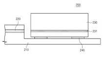
도 2는 평판형 광 도파로와 광 소자 및 전기 소자가 결합된 제 2 예에 따른 광 통신 모듈(200)을 보여준다. 도 2를 참조하면, 광 통신 모듈(200)은 평판형 광 도파로(210), 광 소자(230), 그리고 솔더(240, solder)를 포함한다.2 shows an
광 도파로(210)는 광 신호를 도파하는 광 도파로 코어(220)를 포함한다. 평판형 광 도파로(210)의 일부가 식각되고, 식각된 위치에 광 소자(230)가 형성될 수 있다. 광 소자(230)는 광 도파로(231)를 갖는 도파로형 광 소자를 포함할 수 있다. 광 소자(230)의 광 도파로는 평판형 광 도파로(210)의 광 도파로 코어(220)와 정렬될 수 있다. 즉, 평판형 광 도파로(210)의 광 도파로 코어(220)를 통해 도파되는 광 신호는 광 소자(230)의 광 도파로(231)로 전달될 수 있다. 솔더(240)는 광 소자(230)와 평판형 광 도파로(210)를 고정할 수 있다.The
실리카(silica)로 제조되는 평판형 광 도파로(210)에서, 광 도파로 코어(220)는 평판형 광 도파로(210)의 상부면으로부터 20um 정도 아래에 위치한다. 따라서, 광 소자(230)를 평판형 광 도파로(210)의 위에 형성하고 광 결합을 하기 위해서는 평판형 광 도파로(210)가 20um 이상 식각되어야 한다. 식각 깊이는 광 소자(230)의 정렬 오차를 감안하여 최대한 정밀하게 설정되어야 한다. 그런데, 20um 이상을 식각하면서 식각 오차/편차를 기준값 이하로 유지하기가 어렵기 때문에, 광 정렬이 정상적으로 이루어지기 어렵고, 높은 수율을 확보하기 어렵다.In the planar
도 3는 평판형 광 도파로와 광 소자 및 전기 소자가 결합된 제 3 예에 따른 광 통신 모듈(300)을 보여준다. 도 3을 참조하면, 광 통신 모듈(300)은 금속 블록(310), 전기 소자(320), 광 소자(330), 본딩 배선(340), 그리고 평판형 광 도파로(350)를 포함한다.3 shows an
금속 블록(310)은 광 통신 모듈(300)을 둘러싸는 하우징일 수 있다. 전기 소자(320)는 금속 블록(310)의 상부면에 형성되고, 에폭시(321)와 같은 물질로 금속 블록(310)에 부착될 수 있다. 광 소자(330)는 금속 블록(310)의 상부면에 형성되고, 에폭시(331)와 같은 물질로 금속 블록(310)에 부착될 수 있다. 배선(340)은 전기 소자(320)와 광 소자(330)를 서로 연결할 수 있다.The
평판형 광 도파로(350)는 금속 블록의 일 측면에 에폭시(351)와 같은 물질로 부착될 수 있다. 평판형 광 도파로(350)는 광 소자(330)의 도파로와 광 정렬될 수 있다.The planar
금속 블록(310)의 열 팽창 계수와 평판형 광 도파로(350)의 열 팽창 계수는 서로 다를 수 있다. 금속 블록(310)의 열 팽창 계수와 평판형 광 도파로(350)의 열 팽창 계수가 서로 다르면, 온도가 변화할 때 평판형 광 도파로(350)와 금속 블록(310)의 연결부에 스트레스가 인가되고, 평판형 광 도파로(350)와 광 소자(330)의 광 정렬이 어긋날 수 있다.The coefficient of thermal expansion of the
도 4는 예시적인 물질들의 열 팽창 계수들을 보여준다. 도 3 및 도 4를 참조하면, 금속 블록(310)은 구리(Cu)를 포함할 수 있다. 구리(Cu)의 열 팽창 계수는 16.6이다. 광 소자(330)는 인듐인(InP) 또는 갈륨비소(GaAs)를 포함할 수 있다. 인듐인(InP) 및 갈륨비소(GaAs)의 열 팽창 계수는 각각 4.6 및 5.73이다. 평판형 광 도파로(350)는 실리콘(Si) 또는 쿼츠(Quartz)를 포함할 수 있다. 실리콘(Si) 및 쿼츠(Quartz)의 열 팽창 계수는 각각 2.6 및 0.77 내지 1.4 이다. 금속 블록(310)과 다른 물질들의 열 팽창 계수의 차이가 크므로, 금속 블록(310)에 다른 물질들이 부착되면, 부착 부분이 어긋날 수 있다.4 shows thermal expansion coefficients of exemplary materials. 3 and 4, the
도 5는 실리콘 광 벤치(SiOB)에 광섬유를 고정해서 만든 광 섬유 어레이를 구비한 밸런스 광 수신기의 광 전류를 온도 테스트의 전후에 측정한 결과를 보여준다. 온도 테스트는 섭씨 -40도와 80도 사이를 20회 왕복하는 방법을 사용하였고, 총 테스트 시간은 900분이다. 도 5를 참조하면, 온도 테스트가 수행된 후에 광 전류가 크게 감소한 것으로 나타난다. 즉, 도 3과 같은 광 통신 모듈(300)에서, 온도 변화는 광 정렬의 어긋남을 초래하고, 이에 따라 광 통신 모듈(300)의 신뢰성의 처하를 유발할 수 있다.5 shows the results of measuring the optical current of a balanced optical receiver with an optical fiber array made by fixing an optical fiber to a silicon optical bench (SiOB) before and after a temperature test. The temperature test used a 20 round trip between -40 degrees Celsius and 80 degrees Celsius, with a total test time of 900 minutes. Referring to FIG. 5, it appears that the photocurrent is greatly reduced after the temperature test is performed. That is, in the
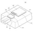
도 6은 본 발명의 제 1 실시 예에 따른 광 통신 모듈(400)을 보여준다. 도 6을 참조하면, 광 통신 모듈(600)은 금속 블록(410), 전기 소자(420), 광 소자 부착 블록(430), 광 소자(440), 본딩 배선(450), 그리고 평판형 광 도파로(460)를 포함한다.6 shows an
금속 블록(410)은 광 통신 모듈(400)을 둘러싸는 하우징일 수 있다. 금속 블록(410)은 광 통신 모듈(400)의 접지 노드로 사용될 수 있다. 금속 블록(410)은 제 1 상부면 및 제 1 상부면보다 낮은 제 2 상부면을 구비한 계단 구조를 가질 수 있다.The
전기 소자(420)는 금속 블록(410)의 제 1 상부면(더 높은 상부면)의 위에 형성된다. 전기 소자(420)는 은 에폭시(silver epoxy)와 같은 도전성 물질(421)을 이용하여 금속 블록(410)의 제 1 상부면에 부착될 수 있다. 전기 소자(420)는 광 소자(440)로부터 배선(450)을 통해 출력되는 전기 신호를 처리할 수 있다. 또는, 전기 소자(420)는 광 소자(440)에 배선(450)을 통해 전기 신호를 공급할 수 있다. 전기 소자(420)는 증폭기, 변조기, 복조기, 또는 프로세서를 포함할 수 있다.
광 소자 부착 블록(430)은 금속 블록(410)의 제 2 상부면(더 낮은 상부면)의 위에 형성된다. 광 소자 부착 블록(430)은 은 에폭시와 같은 도전성 물질(431)을 이용하여 금속 블록(410)의 제 2 상부면의 위에 부착될 수 있다. 광 소자 부착 블록(430)은 금속 블록(410)의 제 1 상부면과 제 2 상부면 사이의 측면에도 부착될 수 있다.The optical
광 소자(440)는 광 소자 부착 블록(430)의 상부면의 위에 형성된다. 광 소자(440)는 은 에폭시와 같은 도전성 물질(441)을 이용하여 광 소자 부착 블록(430)의 상부면의 위에 부착될 수 있다. 광 소자(440)는 광 도파로를 구비한 도파로형 광 소자를 포함할 수 있다. 광 소자(440)는 평판형 광 도파로(460)로부터 수신되는 광 신호를 전기 신호로 변환하고, 변환된 전기 신호를 배선(450)을 통해 전기 소자(420)에 전달할 수 있다. 또는, 광 고자(440)는 전기 소자(420)로부터 배선(450)을 통해 전기 신호를 수신하고, 이를 광 신호로 변환하여 평판형 광 도파로(460)로 송신할 수 있다. 광 소자(440)는 전기 소자(420)로부터 수신되는 전기 신호를 광 신호로 변환하고, 변환된 광 신호를 평판형 광 도파로로 출력할 수 있다. 광 소자(440)는 포토 다이오드, 레이더 다이오드, 광 증폭기, 광 변조기, 또는 광 복조기를 포함할 수 있다.The
본딩 배선(450)은 전기 소자(420) 및 광 소자(440)를 서로 연결할 수 있다.The
평판형 광 도파로(460)는 광 소자 부착 블록(430)의 측면에 부착될 수 있다. 평판형 광 도파로(460)는 자외선 경화 에폭시와 같은 물질(461)을 이용하여 광 소자 부착 블록(430)에 부착될 수 있다. 평판형 광 도파로(460)는 광 소자(440)의 도파로와 광 정렬될 수 있다.The planar
광 소자 부착 블록(430)은 평판형 광 도파로(460)와 동일한(또는 유사한) 열팽창 계수를 갖는 물질을 포함할 수 있다. 광 소자 부착 블록(430)은 평판형 광 도파로(460)의 열 팽창 계수와 기준값(예를 들어, 평판형 광 도파로(460)의 열 팽창 계수의 1%, 5%, 10% 등) 이내의 오차를 갖는 열 팽창 계수를 가질 수 있다. 광 소자 부착 블록(430)은 평판형 광 도파로(460)와 동일한 물질을 포함할 수 있다. 광 소자 부착 블록(430)은 실리콘(Si) 또는 쿼츠(Quartz)를 포함할 수 있다.The optical
광 소자 부착 블록(430)의 열 팽창 계수가 평판형 광 도파로(460)의 열 팽창 계수와 동일(또는 유사)하면, 온도가 변화해도 광 소자 부착 블록(430)과 평판형 광 도파로(460)의 연결부에 스트레스가 가해지지 않을 수 있다. 즉, 온도가 변화해도 높은 신뢰성을 유지하는 광 통신 모듈(400)이 제공된다. 또한, 렌즈나 거울과 같은 추가적인 소자들이 요구되지 않고, 평판형 광 도파로(460)를 광 소자 부착 블록(430)에 단순히 결합하는 것으로 광 정렬이 이루어지므로, 광 통신 모듈(400)의 제조 비용이 감소한다.If the thermal expansion coefficient of the optical
도 7은 본 발명의 제 2 실시 예에 따른 광 통신 모듈(500)을 보여준다. 도 7을 참조하면, 광 통신 모듈(500)은 금속 블록(510), 전기 소자(520), 광 소자 부착 블록(530), 광 소자(540), 본딩 배선(550), 그리고 평판형 광 도파로(560)를 포함한다.7 shows an
도 6의 광 통신 모듈(400)과 비교하면, 전기 소자(520)를 금속 블록(510)에 부착하는 물질과 광 소자(540)를 광 소자 부착 블록(530)에 부착하는 물질은 서로 연결되어 하나의 물질(541)을 형성한다. 이 물질(541)은 은 에폭시와 같은 도전성 물질을 포함할 수 있다. 광 소자(540)가 접지 노드를 필요로 하는 경우, 도 7에 도시된 바와 같이 광 소자(540)가 은 에폭시와 같은 도전성을 갖는 물질(541)을 통해 금속 블록(510)에 연결될 수 있다.Compared with the
도 8은 제 3 실시 예에 따른 광 통신 모듈(600)을 보여준다. 도 8을 참조하면, 광 통신 모듈(600)은 금속 블록(610), 전기 소자(620), 광 소자 부착 블록(630), 광 소자(640), 본딩 배선(650), 그리고 평판형 광 도파로(660)를 포함한다.8 shows an
도 6의 광 통신 모듈(400)과 비교하면, 광 소자 부착 블록(630)의 위에 금속 물질(643)이 제공된다. 금속 물질(643)은 광 소자 부착 블록(630)의 상부면에 증착되는 물질일 수 있다. 광 소자(640)는 은 에폭시와 같은 도전 물질을 이용하여 금속 물질(643)의 위에 부착된다. 금속 물질(643)은 배선(670)을 통해 금속 블록(610)과 연결된다. 광 소자(640)가 접지 노드를 필요로 하는 경우, 도 8에 도시된 바와 같이 광 소자(640)가 금속 물질(643) 및 배선(670)을 통해 금속 블록(510)에 연결될 수 있다.Compared with the
도 9는 본 발명의 실시 예에 따른 광 통신 모듈의 제조 방법을 보여주는 순서도이다. 도 9를 참조하면, S110 단계에서, 제 1 상부면 및 제 1 상부면보다 낮은 제 2 상부면을 포함하는 계단 형태를 갖는 금속 블록이 형성된다.9 is a flowchart illustrating a method of manufacturing an optical communication module according to an embodiment of the present invention. Referring to FIG. 9, in step S110, a metal block having a stair shape including a first upper surface and a second upper surface lower than the first upper surface is formed.
S120 단계에서 금속 블록의 제 2 상부면의 위에 광 소자 부착 블록이 형성되고, S130 단계에서 금속 블록의 제 1 상부면의 위에 전기 소자가 부착된다. S140 단계에서 광 소자 부착 블록의 상부면의 위에 도파로형 광 소자가 부착되고, S150 단계에서 전기 소자 및 도파로형 광 소자가 본딩 배선을 이용하여 서로 연결된다. 이후에, S160 단계에서, 광 소자 부착 블록의 일 측면에 평판형 광 도파로가 부착된다.In operation S120, the optical element attachment block is formed on the second upper surface of the metal block, and in step S130, the electrical element is attached on the first upper surface of the metal block. In step S140, the waveguide type optical element is attached to the upper surface of the optical element attachment block, and in step S150, the electric element and the waveguide type optical element are connected to each other using a bonding wire. Subsequently, in step S160, a flat optical waveguide is attached to one side of the optical element attachment block.
본 발명의 상세한 설명에서는 구체적인 실시 예에 관하여 설명하였으나, 본 발명의 범위와 기술적 사상에서 벗어나지 않는 한도 내에서 여러 가지 변형이 가능하다. 그러므로 본 발명의 범위는 상술한 실시 예에 국한되어 정해져서는 안되며 후술하는 특허청구범위뿐만 아니라 이 발명의 특허청구범위와 균등한 것들에 의해 정해져야 한다.While the invention has been shown and described with reference to certain preferred embodiments thereof, it will be understood by those skilled in the art that various changes and modifications may be made without departing from the spirit and scope of the invention. Therefore, the scope of the present invention should not be limited to the above-described embodiments, but should be determined by the claims equivalent to the claims of the present invention as well as the claims of the following.
100; 광 통신 모듈
110; 금속 패키지120; 세라믹 패키지
130; 광 소자140; 히트 싱크
150; 전기 소자160; 윈도우
170; 평판형 광 도파로180; 렌드들
190; 거울
200; 광 통신 모듈
210; 평판형 광 도파로220; 광 도파로 코어
230; 광 소자231; 광 도파로
240; 솔더
300; 광 통신 모듈
310; 금속 블록320; 전기 소자
330; 광 소자340; 본딩 배선
350; 평판형 광 도파로
400, 500, 600; 광 통신 모듈
410, 510, 610; 금속 블록420, 520, 620; 전기 소자
430, 530, 630; 광 소자 부착 블록440, 540, 640; 광 소자
450, 550, 650; 본딩 배선460, 560, 660; 평판형 광 도파로
670; 배선100; Optical communication module
110;
130;
150;
170; Flat
190; mirror
200; Optical communication module
210; Flat
230;
240; Solder
300; Optical communication module
310; Metal block 320; Electrical elements
330;
350; Planar Optical Waveguide
400, 500, 600; Optical communication module
410, 510, 610; Metal blocks 420, 520, 620; Electrical elements
430, 530, 630; Optical element attachment blocks 440, 540, 640; Optical element
450, 550, 650;
670; Wiring
Claims (14)
Translated fromKorean상기 금속 블록 위에 형성되는 전기 소자;
상기 금속 블록의 위에 형성되는 광 소자 부착 블록;
상기 광 소자 부착 블록의 위에 형성되고, 상기 전기 소자와 본딩 배선을 통해 연결되는 광 소자; 그리고
상기 광 소자 부착 블록의 일 측면에 형성되고, 상기 광 소자와 광 정렬되는 평판형 광 도파로를 포함하는 광 통신 모듈.Metal blocks;
An electrical element formed over the metal block;
An optical element attachment block formed on the metal block;
An optical element formed on the optical element attachment block and connected to the electrical element through a bonding line; And
And a flat plate optical waveguide formed on one side of the optical element attachment block and optically aligned with the optical element.
상기 평판형 광 도파로는 상기 광 소자 부착 블록의 일 측면에 부착되는 광 통신 모듈.The method of claim 1,
The flat optical waveguide is attached to one side of the optical element attachment block.
상기 평판형 광 도파로는 상기 광 소자 부착 블록의 일 측면에 자외선 경화 에폭시를 이용하여 부착되는 광 통신 모듈.3. The method of claim 2,
The flat optical waveguide is attached to one side of the optical element attachment block using an ultraviolet curing epoxy.
상기 광 소자 부착 블록은 상기 평판형 광 도파로의 열 팽창 계수와 기준값 이내의 차이를 갖는 열 팽창 계수를 갖는 물질을 포함하는 광 통신 모듈.The method of claim 1,
And the optical element attachment block comprises a material having a thermal expansion coefficient having a difference within a reference value and a thermal expansion coefficient of the flat optical waveguide.
상기 광 소자 부착 블록은 상기 평판형 광 도파로와 동일한 물질을 포함하는 광 통신 모듈.The method of claim 1,
And the optical element attachment block comprises the same material as the planar optical waveguide.
상기 광 소자는 제 1 도전성 물질을 이용하여 상기 광 소자 부착 블록에 부착되고, 상기 전기 소자는 제 2 도전성 물질을 이용하여 상기 금속 블록에 부착되는 광 통신 모듈.The method of claim 1,
And the optical element is attached to the optical element attachment block using a first conductive material, and the electrical element is attached to the metal block using a second conductive material.
상기 제 1 도전성 물질과 제 2 도전성 물질은 서로 연결되는 광 통신 모듈.The method according to claim 6,
And the first conductive material and the second conductive material are connected to each other.
상기 제 1 도전성 물질은 배선을 통해 상기 금속 블록에 연결되는 광 통신 모듈.The method according to claim 6,
And the first conductive material is connected to the metal block via a wire.
상기 제 1 도전성 물질과 제 2 도전성 물질 각각은 은 에폭시를 포함하는 광 통신 모듈.The method according to claim 6,
And wherein each of the first conductive material and the second conductive material comprises a silver epoxy.
상기 광 소자 부착 블록의 위에 형성되는 금속 판을 더 포함하고,
상기 광 소자는 상기 제 1 도전성 물질을 이용하여 상기 금속 판의 위에 부착되고,
상기 금속 판은 배선을 통해 상기 금속 블록과 연결되는 광 통신 모듈.The method according to claim 6,
Further comprising a metal plate formed on the optical element attachment block,
The optical element is attached onto the metal plate using the first conductive material,
And the metal plate is connected to the metal block through a wire.
상기 광 소자는 도파로형 광 소자를 포함하고,
상기 광 소자의 도파로는 상기 평판형 광 도파로와 광 정렬되는 광 통신 모듈.The method of claim 1,
The optical device includes a waveguide optical device,
And the waveguide of the optical element is optically aligned with the planar optical waveguide.
상기 금속 블록은 제 1 상부면 및 상기 제 1 상부면보다 낮은 제 2 상부면을 포함하는 계단 형태를 갖고,
상기 전기 소자는 상기 금속 블록의 상기 제 1 상부면의 위에 형성되고,
상기 광 소자 부착 블록은 상기 금속 블록의 상기 제 2 상부면의 위에 형성되는 광 통신 모듈.The method of claim 1,
The metal block has a step shape including a first upper surface and a second upper surface lower than the first upper surface,
The electrical element is formed over the first upper surface of the metal block,
And the optical element attachment block is formed above the second upper surface of the metal block.
상기 금속 블록의 상기 제 1 상부면과 상기 광 소자 부착 블록의 상부면은 서로 정렬되는 광 통신 모듈.13. The method of claim 12,
And the first top surface of the metal block and the top surface of the optical element attachment block are aligned with each other.
제 1 상부면 및 상기 제 1 상부면보다 낮은 제 2 상부면을 포함하는 계단 형태를 갖는 금속 블록을 형성하는 단계;
상기 금속 블록의 상기 제 2 상부면의 위에 광 소자 부착 블록을 형성하는 단계;
상기 금속 블록의 상기 제 1 상부면의 위에 전기 소자를 부착하는 단계;
상기 광 소자 부착 블록의 상부면의 위에 도파로형 광 소자를 부착하는 단계;
상기 전기 소자 및 도파로형 광 소자를 본딩 배선을 이용하여 서로 연결하는 단계; 그리고
상기 광 소자 부착 블록의 일 측면에 평판형 광 도파로를 부착하는 단계를 포함하고,
상기 평판형 광 도파로는 상기 도파로형 광 소자의 도파로와 광 정렬되는 광 통신 모듈의 제조 방법.In the manufacturing method of the optical communication module:
Forming a metal block having a step shape including a first upper surface and a second upper surface lower than the first upper surface;
Forming an optical element attachment block on the second upper surface of the metal block;
Attaching an electrical element over the first top surface of the metal block;
Attaching a waveguide optical element on an upper surface of the optical element attachment block;
Connecting the electrical element and the waveguide optical element to each other using a bonding line; And
Attaching a planar optical waveguide to one side of the optical element attachment block,
The flat optical waveguide is optically aligned with the waveguide of the waveguide optical element.
Priority Applications (2)
| Application Number | Priority Date | Filing Date | Title |
|---|---|---|---|
| KR1020110138237AKR20130070956A (en) | 2011-12-20 | 2011-12-20 | Optical communication module and method of producting optical communication module |
| US13/611,119US20130156394A1 (en) | 2011-12-20 | 2012-09-12 | Optical communication module and method of manufacturing the same |
Applications Claiming Priority (1)
| Application Number | Priority Date | Filing Date | Title |
|---|---|---|---|
| KR1020110138237AKR20130070956A (en) | 2011-12-20 | 2011-12-20 | Optical communication module and method of producting optical communication module |
Publications (1)
| Publication Number | Publication Date |
|---|---|
| KR20130070956Atrue KR20130070956A (en) | 2013-06-28 |
Family
ID=48610243
Family Applications (1)
| Application Number | Title | Priority Date | Filing Date |
|---|---|---|---|
| KR1020110138237AWithdrawnKR20130070956A (en) | 2011-12-20 | 2011-12-20 | Optical communication module and method of producting optical communication module |
Country Status (2)
| Country | Link |
|---|---|
| US (1) | US20130156394A1 (en) |
| KR (1) | KR20130070956A (en) |
Families Citing this family (1)
| Publication number | Priority date | Publication date | Assignee | Title |
|---|---|---|---|---|
| JP6530706B2 (en)* | 2015-12-25 | 2019-06-12 | 日本電信電話株式会社 | Optical device |
Family Cites Families (3)
| Publication number | Priority date | Publication date | Assignee | Title |
|---|---|---|---|---|
| US5206986A (en)* | 1989-08-11 | 1993-05-04 | Fujitsu Limited | Method of producing an electronic circuit package |
| US5835650A (en)* | 1995-11-16 | 1998-11-10 | Matsushita Electric Industrial Co., Ltd. | Optical apparatus and method for producing the same |
| US6608950B2 (en)* | 2001-02-14 | 2003-08-19 | Northrop Grumman Corporation | Integrated optoelectronic device and method for making same |
- 2011
- 2011-12-20KRKR1020110138237Apatent/KR20130070956A/ennot_activeWithdrawn
- 2012
- 2012-09-12USUS13/611,119patent/US20130156394A1/ennot_activeAbandoned
Also Published As
| Publication number | Publication date |
|---|---|
| US20130156394A1 (en) | 2013-06-20 |
Similar Documents
| Publication | Publication Date | Title |
|---|---|---|
| US11256046B2 (en) | Photonic interface for electronic circuit | |
| US11163126B2 (en) | Light source assembly supporting direct coupling to an integrated circuit | |
| US10454586B2 (en) | Integrated transceiver with lightpipe coupler | |
| JP4790819B2 (en) | Method and system for a hybrid integrated 1xN DWDN transmitter | |
| CN101517937B (en) | Method and system for integrating a DWDM receiver | |
| EP1723456B1 (en) | System and method for the fabrication of an electro-optical module | |
| Ambrosy et al. | Silicon motherboards for multichannel optical modules | |
| KR20130070956A (en) | Optical communication module and method of producting optical communication module | |
| Bolle et al. | Compact Hybridly Integrated 10$\,\times\, $11.1-Gb/s DWDM Optical Receiver | |
| Peall | Hybrid Integration of Optical Devices on Silicon |
Legal Events
| Date | Code | Title | Description |
|---|---|---|---|
| PA0109 | Patent application | Patent event code:PA01091R01D Comment text:Patent Application Patent event date:20111220 | |
| PG1501 | Laying open of application | ||
| PC1203 | Withdrawal of no request for examination | ||
| WITN | Application deemed withdrawn, e.g. because no request for examination was filed or no examination fee was paid |