KR20130062920A - Semiconductor device - Google Patents
Semiconductor deviceDownload PDFInfo
- Publication number
- KR20130062920A KR20130062920AKR1020127027699AKR20127027699AKR20130062920AKR 20130062920 AKR20130062920 AKR 20130062920AKR 1020127027699 AKR1020127027699 AKR 1020127027699AKR 20127027699 AKR20127027699 AKR 20127027699AKR 20130062920 AKR20130062920 AKR 20130062920A
- Authority
- KR
- South Korea
- Prior art keywords
- oxide semiconductor
- layer
- semiconductor layer
- transistor
- electrode layer
- Prior art date
- Legal status (The legal status is an assumption and is not a legal conclusion. Google has not performed a legal analysis and makes no representation as to the accuracy of the status listed.)
- Granted
Links
Images


Classifications
- H—ELECTRICITY
- H10—SEMICONDUCTOR DEVICES; ELECTRIC SOLID-STATE DEVICES NOT OTHERWISE PROVIDED FOR
- H10D—INORGANIC ELECTRIC SEMICONDUCTOR DEVICES
- H10D30/00—Field-effect transistors [FET]
- H10D30/60—Insulated-gate field-effect transistors [IGFET]
- H10D30/67—Thin-film transistors [TFT]
- H10D30/6728—Vertical TFTs
- H—ELECTRICITY
- H10—SEMICONDUCTOR DEVICES; ELECTRIC SOLID-STATE DEVICES NOT OTHERWISE PROVIDED FOR
- H10D—INORGANIC ELECTRIC SEMICONDUCTOR DEVICES
- H10D30/00—Field-effect transistors [FET]
- H10D30/60—Insulated-gate field-effect transistors [IGFET]
- H10D30/67—Thin-film transistors [TFT]
- H10D30/6729—Thin-film transistors [TFT] characterised by the electrodes
- H10D30/673—Thin-film transistors [TFT] characterised by the electrodes characterised by the shapes, relative sizes or dispositions of the gate electrodes
- H10D30/6733—Multi-gate TFTs
- H—ELECTRICITY
- H10—SEMICONDUCTOR DEVICES; ELECTRIC SOLID-STATE DEVICES NOT OTHERWISE PROVIDED FOR
- H10D—INORGANIC ELECTRIC SEMICONDUCTOR DEVICES
- H10D30/00—Field-effect transistors [FET]
- H10D30/60—Insulated-gate field-effect transistors [IGFET]
- H10D30/67—Thin-film transistors [TFT]
- H10D30/674—Thin-film transistors [TFT] characterised by the active materials
- H10D30/6755—Oxide semiconductors, e.g. zinc oxide, copper aluminium oxide or cadmium stannate
Landscapes
- Thin Film Transistor (AREA)
Abstract
Translated fromKorean
Description
Translated fromKorean본 발명의 기술 분야는 산화물 반도체를 사용하는 반도체 장치에 관한 것이다.The technical field of the present invention relates to a semiconductor device using an oxide semiconductor.
최근에, 평판형 표시들로 대표되는 많은 액정 표시 장치들 및 발광 표시 장치들에 사용되는 트랜지스터들은 비정질 실리콘 또는 다결정 실리콘과 같은 실리콘 반도체를 포함하고 유리 기판들 위에 형성된다.Recently, many liquid crystal display devices and light emitting display devices represented by flat panel displays include silicon semiconductors such as amorphous silicon or polycrystalline silicon and are formed on glass substrates.
실리콘 반도체 대신, 산화물 반도체가 트랜지스터들에 사용되는 기술이 주목받고 있다.Instead of silicon semiconductors, a technique in which oxide semiconductors are used in transistors is drawing attention.
산화물 반도체의 예들로는 1원계 금속 산화물인 산화아연 및 호모러거스(homologous) 화합물인 In-Ga-Zn-O계 산화물 반도체가 있다. 또한, 트랜지스터들이 이들 산화물 반도체들을 사용하여 형성되고 트랜지스터들이 표시 장치들에 있어서의 화소들의 스위칭 소자들 등에 사용되는 기술들이 개시되어 있다(특허문헌 1 및 특허문헌 2 참조).Examples of oxide semiconductors include zinc oxide, which is a primary metal oxide, and In-Ga-Zn-O, which is a homologous compound. In addition, techniques are disclosed in which transistors are formed using these oxide semiconductors and transistors are used for switching elements of pixels and the like in display devices (see Patent Document 1 and Patent Document 2).
보텀-게이트형 트랜지스터는 드레인 전류가 수평 방향으로 소스 및 드레인 사이에서 흐르기 때문에 수평형 트랜지스터라고 말할 수 있다. 큰 드레인 전류가 흐를 수 있도록 하기 위해서 수평형 트랜지스터의 크기를 증가시킬 필요가 있다. 따라서, 수평형 트랜지스터는 전력 디바이스와 같은 고 전력 응용을 위한 반도체 장치에 적합하다고 말할 수 없다.The bottom-gate transistor can be said to be a horizontal transistor because drain current flows between the source and the drain in the horizontal direction. In order to allow a large drain current to flow, it is necessary to increase the size of the horizontal transistor. Thus, horizontal transistors cannot be said to be suitable for semiconductor devices for high power applications such as power devices.
고 전력 응용을 위한 반도체 장치로서, 채널 영역으로서 작용하는 반도체층이 소스 전극층 및 드레인 전극층과 중첩하고 드레인 전류의 방향이 반도체층의 두께 방향인 수직형 트랜지스터가 바람직하다고 말할 수 있다. 이것은, 이들 트랜지스터들이 동일하거나 실질적으로 동일한 양의 드레인 전류가 흐를 수 있도록 형성될 때, 수직형 트랜지스터가 수평형 트랜지스터보다 작게(더 작은 면적을 갖도록) 형성될 수 있기 때문이다.As a semiconductor device for high power application, it can be said that a vertical transistor in which a semiconductor layer serving as a channel region overlaps with a source electrode layer and a drain electrode layer and the direction of the drain current is in the thickness direction of the semiconductor layer is preferable. This is because when these transistors are formed such that the same or substantially the same amount of drain current can flow, the vertical transistors can be formed smaller (having a smaller area) than the horizontal transistors.
다양한 구조들의 수직형 트랜지스터들이 있다. 수직형 트랜지스터의 게이트 전극층이 반도체층의 측면에 인접하여 형성될 때, 큰 드레인 전류를 얻기 위해 수직형 트랜지스터의 드레인 전극층 및 소스 전극층 각각의 폭이 증가되어(채널 영역의 폭이 증가되어), 반도체층의 측면에 인접하여 형성된 게이트 전극층으로부터 반도체층에 인가되는 전계가 불충분하게 될 수 있다.There are vertical transistors of various structures. When the gate electrode layer of the vertical transistor is formed adjacent to the side of the semiconductor layer, the width of each of the drain electrode layer and the source electrode layer of the vertical transistor is increased (the width of the channel region is increased) in order to obtain a large drain current, thereby the semiconductor An electric field applied to the semiconductor layer from the gate electrode layer formed adjacent to the side of the layer may become insufficient.
또한, 고 전력 응용을 위한 반도체 장치는 높은 파괴 전압, 높은 변환 효율, 또는 고속 스위칭과 같은 속성들을 갖는 구조 및 큰 드레인 전류가 흐를 수 있는 구조를 가질 필요가 있다.In addition, semiconductor devices for high power applications need to have a structure having properties such as high breakdown voltage, high conversion efficiency, or high speed switching, and a structure in which a large drain current can flow.
따라서, 상기 사항들을 고려하면, 본 발명의 일 실시형태의 목적은 양호한 속성들을 갖는 고 전력 응용을 위한 반도체 장치를 제공하는 것이다.Accordingly, in view of the above, it is an object of an embodiment of the present invention to provide a semiconductor device for high power application having good attributes.
본 발명의 일 실시형태에 따르면, 수직형 트랜지스터의 게이트 전극층의 일부는 소스 전극층, 드레인 전극층, 및 채널 영역으로서 작용하는 반도체층의 일부들과 중첩한다. 이 구조에 의하면, 게이트 전극층은 채널 영역으로서 작용하는 반도체층에 충분히 높은 전계를 인가할 수 있다.According to one embodiment of the present invention, a portion of the gate electrode layer of the vertical transistor overlaps with a portion of the semiconductor layer serving as the source electrode layer, the drain electrode layer, and the channel region. According to this structure, the gate electrode layer can apply a sufficiently high electric field to the semiconductor layer serving as the channel region.
또한, 고 전력 응용을 위한 반도체 장치에 필요한 상술된 속성들을 향상시키는 반도체 재료로서, 산화물 반도체가 사용되는 것이 바람직하다.In addition, it is preferable that an oxide semiconductor be used as the semiconductor material to improve the above-described properties required for the semiconductor device for high power application.
산화물 반도체는 실리콘 반도체의 2배 이상인 밴드 갭을 갖고; 따라서, 산화물 반도체는 반도체 장치의 파괴 전압의 개선, 전력 손실의 감소 등의 이점들을 갖는다.The oxide semiconductor has a band gap that is twice as large as that of the silicon semiconductor; Therefore, the oxide semiconductor has advantages such as improvement of breakdown voltage of the semiconductor device, reduction of power loss, and the like.
본 발명의 일 실시형태는 소스 전극층; 소스 전극층과 접하는 산화물 반도체층; 산화물 반도체층과 접하는 드레인 전극층; 소스 전극층, 드레인 전극층 및 산화물 반도체층과 중첩하는 게이트 전극층의 일부; 및 게이트 전극층의 전체 표면과 접하는 게이트 절연층을 포함하는 트랜지스터이다. 게이트 전극층의 하면 측 상의 게이트 절연층은 소스 전극층과 접하고, 게이트 전극층의 상면 측 상의 게이트 절연층은 산화물 반도체층과 접한다.One embodiment of the invention the source electrode layer; An oxide semiconductor layer in contact with the source electrode layer; A drain electrode layer in contact with the oxide semiconductor layer; A portion of the gate electrode layer overlapping the source electrode layer, the drain electrode layer, and the oxide semiconductor layer; And a gate insulating layer in contact with the entire surface of the gate electrode layer. The gate insulating layer on the lower surface side of the gate electrode layer is in contact with the source electrode layer, and the gate insulating layer on the upper surface side of the gate electrode layer is in contact with the oxide semiconductor layer.
본 발명의 또 다른 실시형태는 소스 전극층; 소스 전극층과 접하는 산화물 반도체층; 산화물 반도체층과 접하는 드레인 전극층; 소스 전극층, 드레인 전극층 및 산화물 반도체층과 중첩하는 게이트 전극층의 일부; 및 게이트 전극층의 전체 표면과 접하는 게이트 절연층을 포함하는 트랜지스터이다. 게이트 전극층의 하면 측 및 상면 측 상의 게이트 절연층은 산화물 반도체층과 접한다.Yet another embodiment of the present invention includes a source electrode layer; An oxide semiconductor layer in contact with the source electrode layer; A drain electrode layer in contact with the oxide semiconductor layer; A portion of the gate electrode layer overlapping the source electrode layer, the drain electrode layer, and the oxide semiconductor layer; And a gate insulating layer in contact with the entire surface of the gate electrode layer. The gate insulating layer on the lower surface side and the upper surface side of the gate electrode layer is in contact with the oxide semiconductor layer.
상술된 트랜지스터에 있어서, 제공되는 게이트 전극층들 및 게이트 절연층들의 수에는 특별한 제한이 없다. 산화물 반도체층에 인가되는 전계를 증가시키기 위해 2개의 게이트 전극층들 및 2개의 게이트 절연층들이 제공될 수 있고, 산화물 반도체층을 개재하여 대향하는 한 쌍의 게이트 전극층들 및 산화물 반도체층을 개재하여 대향하는 한 쌍의 게이트 절연층들이 형성될 수 있다. 대안적으로, 복수의 유닛들로서, 이들 각각에서 상기 한 쌍의 게이트 전극층들이 대향하고 있고 상기 한 쌍의 게이트 절연층들이 대향하고 있는, 상기 복수의 유닛들이 제공될 수 있다. 또한, 대안적으로, 게이트 전극층 및 게이트 절연층은 산화물 반도체층을 둘러싸도록 원형 형태로 제공될 수 있다.In the above-described transistor, there is no particular limitation on the number of gate electrode layers and gate insulating layers provided. Two gate electrode layers and two gate insulating layers may be provided to increase an electric field applied to the oxide semiconductor layer, and face each other via a pair of gate electrode layers and an oxide semiconductor layer opposing through the oxide semiconductor layer. A pair of gate insulating layers may be formed. Alternatively, as a plurality of units, the plurality of units may be provided in each of which the pair of gate electrode layers are opposed and the pair of gate insulating layers are opposite. Alternatively, the gate electrode layer and the gate insulating layer may be provided in a circular shape to surround the oxide semiconductor layer.
산화물 반도체층이 상술된 트랜지스터에서 두껍게 형성될 때, 평탄성이 없어질 수 있고 산화물 반도체층이 박리될 수 있으며; 따라서, 산화물 반도체층에 도전층이 제공되는 것이 바람직하다.When the oxide semiconductor layer is formed thick in the above-described transistor, flatness may be lost and the oxide semiconductor layer may be peeled off; Therefore, it is preferable that a conductive layer is provided in the oxide semiconductor layer.
상술된 방법에 의해 얻어지는 트랜지스터를 통해 큰 드레인 전류가 흐를 수 있고, 트랜지스터는 드레인-파괴-전압 특성들이 높다. 따라서, 본 발명의 일 실시형태는 양호한 속성들을 갖는 고 전력 응용을 위한 반도체 장치를 제공할 수 있다.Large drain currents can flow through the transistor obtained by the method described above, and the transistor has high drain-break-voltage characteristics. Thus, one embodiment of the present invention can provide a semiconductor device for high power applications with good attributes.
도 1a는 트랜지스터의 상면도.
도 1b는 트랜지스터의 단면도.
도 2a는 트랜지스터의 상면도.
도 2b는 트랜지스터의 단면도.
도 3a는 트랜지스터의 상면도.
도 3b는 트랜지스터의 단면도.
도 4a는 트랜지스터의 상면도.
도 4b는 트랜지스터의 단면도.
도 5a는 트랜지스터의 상면도.
도 5b는 트랜지스터의 단면도.
도 6a는 트랜지스터의 상면도.
도 6b는 트랜지스터의 단면도.
도 7a는 트랜지스터의 상면도.
도 7b는 트랜지스터의 단면도.
도 8a는 트랜지스터의 상면도.
도 8b는 트랜지스터의 단면도.
도 9a 내지 도 9c는 트랜지스터를 제작하기 위한 방법을 도시하는 단면도.
도 10a 및 도 10b는 트랜지스터를 제작하기 위한 방법을 도시하는 단면도.
도 11a 내지 도 11d는 트랜지스터를 제작하기 위한 방법을 도시하는 단면도.
도 12a 내지 도 12d는 트랜지스터를 제작하기 위한 방법을 도시하는 단면도.
도 13a 내지 도 13e는 트랜지스터를 제작하기 위한 방법을 도시하는 단면도.
도 14는 태양광발전 시스템의 예를 도시하는 도면.1A is a top view of a transistor.
1B is a cross-sectional view of a transistor.
2A is a top view of a transistor.
2B is a cross-sectional view of the transistor.
3A is a top view of a transistor.
3B is a cross-sectional view of the transistor.
4A is a top view of a transistor.
4B is a cross-sectional view of the transistor.
5A is a top view of a transistor.
5B is a cross-sectional view of the transistor.
6A is a top view of the transistor.
6B is a cross-sectional view of the transistor.
7A is a top view of a transistor.
7B is a cross-sectional view of the transistor.
8A is a top view of a transistor.
8B is a cross-sectional view of the transistor.
9A-9C are cross-sectional views illustrating a method for fabricating a transistor.
10A and 10B are cross-sectional views illustrating a method for fabricating a transistor.
11A-11D are cross-sectional views illustrating a method for fabricating a transistor.
12A-12D are cross-sectional views illustrating a method for fabricating a transistor.
13A-13E are cross-sectional views illustrating a method for fabricating a transistor.
14 shows an example of a photovoltaic system.
본 발명의 실시형태들은 이하 첨부 도면들을 참조하여 상세히 기술된다. 본 발명은 다음 설명으로 제한되지 않고, 당업자들은 모드들 및 세부사항들이 본 발명의 정신 및 범위를 벗어나지 않고 다양한 방식들로 수정될 수 있다는 것이 쉽게 인식할 것이라는 것을 유념해야 한다. 따라서, 본 발명은 다음 실시형태들의 기술로 제한되는 것으로 이해되어서는 안 된다. 이하 기술되는 본 발명의 구조들에 있어서, 동일한 부분들 또는 유사한 기능들을 갖는 부분들은 상이한 도면들에서 동일한 참조부호들로 표기되고, 그 설명은 반복되지 않는다는 것을 유념해야 한다.Embodiments of the present invention are described in detail below with reference to the accompanying drawings. It should be noted that the present invention is not limited to the following description, and those skilled in the art will readily recognize that modes and details may be modified in various ways without departing from the spirit and scope of the present invention. Therefore, the present invention should not be understood as being limited to the description of the following embodiments. In the structures of the present invention described below, it should be noted that parts having the same parts or similar functions are denoted by the same reference numerals in different drawings, and the description is not repeated.
본 명세서의 도면들에 도시되어 있는 각 구조의 크기, 층의 두께, 또는 영역은 어떤 경우들에 있어서는 간결성을 위해서 과장되어 있다. 따라서, 본 발명의 실시형태들은 이러한 스케일들로 제한되지 않는다.The size, thickness, or area of each structure shown in the figures herein is exaggerated in some cases for brevity. Thus, embodiments of the present invention are not limited to these scales.
본 명세서에 있어서, "온-상태 전류"는 박막 트랜지스터가 온 상태에 있을 때 소스 및 드레인 간에 흐르는 전류라는 것을 유념해야 한다. 예를 들어, n-채널 박막 트랜지스터의 경우에, 온-상태 전류는 트랜지스터의 게이트 전압이 그 임계 전압보다 높을 때 소스 및 드레인 간에 흐르는 전류이다. 또한, "오프-상태 전류"는 박막 트랜지스터가 오프 상태에 있을 때 소스 및 드레인 간에 흐르는 전류이다. 예를 들어, n-채널 박막 트랜지스터의 경우에, 오프-상태 전류는 트랜지스터의 게이트 전압이 그 임계 전압보다 낮을 때 소스 및 드레인 간에 흐르는 전류이다. 여기서, "게이트 전압"은 소스의 전위가 기준 전위로서 사용될 때 소스 및 게이트 간의 전위차를 말한다는 것을 유념해야 한다.In the present specification, it should be noted that the "on-state current" is a current flowing between the source and the drain when the thin film transistor is in the on state. For example, in the case of an n-channel thin film transistor, the on-state current is the current flowing between the source and the drain when the gate voltage of the transistor is above its threshold voltage. Also, the "off-state current" is the current flowing between the source and the drain when the thin film transistor is in the off state. For example, in the case of an n-channel thin film transistor, the off-state current is the current flowing between the source and drain when the gate voltage of the transistor is below its threshold voltage. Here, it should be noted that the "gate voltage" refers to the potential difference between the source and the gate when the potential of the source is used as the reference potential.
"소스" 및 "드레인"의 기능들은 종종, 예를 들어, 전류 흐름 방향이 회로 동작에서 변경될 때 서로 교환된다. 따라서, 용어 "소스" 및 "드레인"은 본 명세서에서 각각 드레인 및 소스로 표기되어 사용될 수 있다.The functions of "source" and "drain" are often interchanged with each other, for example, when the current flow direction changes in circuit operation. Thus, the terms "source" and "drain" may be used herein as labeled drain and source, respectively.
(실시형태 1)(Embodiment 1)
이 실시형태에 있어서, 트랜지스터(100)의 구조가 도 1a 및 도 1b를 참조하여 기술될 것이다.In this embodiment, the structure of the
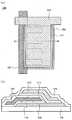
도 1a는 트랜지스터(100)의 상면도이고, 도 1b는 도 1a의 점선 A-B를 따라 취해진 단면도에 해당한다.FIG. 1A is a top view of the
도 1b에 도시되어 있는 것과 같이, 소스 전극층(103)은 기판(101) 위에 제공되고, 게이트 절연층(110) 및 게이트 전극층(107)은 소스 전극층(103) 위에 제공된다. 게이트 절연층(110)은 게이트 전극층(107)의 상면 및 하면을 덥고 소스 전극층(103)과 접한다. 또한, 산화물 반도체층(111)의 하면은 게이트 절연층(110)의 일부 및 소스 전극층(103)의 일부와 접한다. 또한, 드레인 전극층(113)이 산화물 반도체층(111) 위에 제공되고, 보호 절연층(115)이 트랜지스터(100)의 최외층 위에 제공된다.As shown in FIG. 1B, the
트랜지스터(100)에 있어서, 게이트 전극층(107)의 일부는 소스 전극층(103) 및 드레인 전극층(113)과 중첩하고 게이트 절연층(110)을 개재하여 산화물 반도체층(111)으로 덮인다.In the
트랜지스터(100)의 산화물 반도체층(111)은 고순도화된 산화물 반도체층이고 결함 준위들이 감소된 산화물 반도체층이다.The
트랜지스터(100)에 있어서, 게이트 전극층(107)의 일부가 산화물 반도체층(111)으로 덮이기 때문에, 충분히 높은 전계가 산화물 반도체층(111)에 인가될 수 있고; 따라서, 산화물 반도체층(111)의 넓은 면적에 채널 형성 영역이 형성된다. 따라서, 큰 드레인 전류가 트랜지스터(100)를 통해 흐를 수 있다.In the
또한, 산화물 반도체층(111)의 두께를 크게 함으로써, 트랜지스터(100)는 고 전력 응용을 위한 반도체 장치에 필요한 드레인-파괴-전압 특성들을 가질 수 있다. 또한, 게이트 전극층(107) 및 게이트 절연층(110) 각각은 산화물 반도체층(111)의 넓은 면적에 충분히 높은 전계를 인가하기 위해서 콤형(comb shape)을 갖는 것이 바람직하다.In addition, by increasing the thickness of the
기판(101)이 적어도 나중에 수행될 열 처리를 견디기에 충분한 내열성을 갖는다면 기판(101)에는 특별한 제한이 없다. 기판으로서(101), 바륨 보로실리케이트 유리, 알루미노보로실리케이트 유리 등의 유리 기판이 사용될 수 있다.There is no particular limitation on the
유리 기판으로서, 나중에 수행될 열 처리의 온도가 높으면, 변형점이 730℃ 이상인 유리 기판이 사용되는 것이 바람직하다. 유리 기판으로서, 예를 들어, 알루미노실리케이트 유리, 알루미노보로실리케이트 유리, 또는 바륨 보로실리케이트 유리와 같은 유리 재료가 사용된다. BaO의 양이 B2O3보다 많도록 BaO 및 B2O3를 함유하는 유리 기판이 사용되는 것이 바람직하다는 것을 유념해야 한다.As the glass substrate, if the temperature of the heat treatment to be performed later is high, it is preferable that a glass substrate having a strain point of 730 ° C or higher is used. As the glass substrate, for example, a glass material such as aluminosilicate glass, aluminoborosilicate glass, or barium borosilicate glass is used. So that the amount of BaO more than the B2 O3 is a glass substrate containing BaO and B2 O3 it is to be noted that it is preferably used.
세라믹 기판, 석영 기판, 또는 사파이어 기판과 같이 절연체로 형성되는 기판이 유리 기판 대신 사용될 수 있다는 것을 유념해야 한다. 대안적으로, 결정화 유리 등이 사용될 수 있다.It should be noted that a substrate formed of an insulator such as a ceramic substrate, a quartz substrate, or a sapphire substrate may be used instead of the glass substrate. Alternatively, crystallized glass or the like can be used.
소스 전극층(103)은, 몰리브덴, 티타늄, 크롬, 탄탈, 텅스텐, 알루미늄, 구리, 네오디뮴, 스칸듐, 또는 니켈과 같은 금속 재료 또는 주성분으로서 이들 재료들 중 임의의 재료를 포함하는 합금 재료를 사용하는 단층 또는 적층으로서 형성될 수 있다. 또한, 인과 같은 불순물 원소로 도핑되는 다결정 실리콘으로 대표되는 반도체 재료, AgPdCu 합금, Al-Nd 합금, Al-Ni 합금 등이 사용될 수 있다. 소스 전극층(103)은 단층 구조 또는 2개 이상의 층들의 적층 구조를 가질 수 있다. 예를 들어, 실리콘을 함유하는 알루미늄막의 단층 구조, 알루미늄막 위에 티타늄막이 형성되는 2-층 구조, 구리-마그네슘-알루미늄 합금막 위에 구리막이 형성되는 2-층 구조, 텅스텐막 위에 티타늄막이 형성되는 2-층 구조, 티타늄막, 알루미늄막 및 티타늄막이 순서대로 적층되는 3-층 구조 등이 제공될 수 있다.The
또한, 소스 전극층(103)은 인듐 주석 산화물, 산화텅스텐을 함유하는 인듐 산화물, 산화텅스텐을 함유하는 인듐 아연 산화물, 산화티타늄을 함유하는 인듐 산화물, 산화티타늄을 함유하는 인듐 주석 산화물, 인듐 아연 산화물 또는 산화실리콘이 첨가되는 인듐 주석 산화물과 같은 투광성 도전 재료를 사용하여 형성될 수 있다. 상술된 투광성 도전 재료 및 상술된 금속 원소의 적층 구조가 소스 전극층(103)에 이용될 수 있다. 소스 전극층(103)의 두께는 기판(101)에 대한 밀착성, 소스 전극층(103)의 저항률 등을 고려하여 적절히 결정될 수 있다는 것을 유념해야 한다. 예를 들어, 소스 전극층(103)의 두께는 50㎚ 이상 및 500㎚ 이하일 수 있다.The
게이트 절연층(110)은 산화실리콘막, 질화실리콘막, 산화질화실리콘막, 질화산화실리콘막, 산화알루미늄막, 질화알루미늄막, 산화질화알루미늄막, 질화산화알루미늄막, 산화탄탈막, 또는 산화갈륨막으로 형성될 수 있다. 산화물 반도체층(111)과 접하는 게이트 절연층(110)의 일부분은 바람직하게 산소를 함유하고, 특히, 게이트 절연층(110)은 바람직하게 산화실리콘막을 사용하여 형성되는 것이 바람직하다.The
산화하프늄, 산화이트륨, 하프늄 실리케이트(HfSixOy(x>0,y>0)), 질소가 첨가된 하프늄 실리케이트(HfSixOy(x>0,y>0)), 질소가 첨가된 하프늄 알루미네이트(HfAlxOy(x>0,y>0))와 같은 high-k 재료가 사용될 때, 게이트 누설 전류가 감소될 수 있다.Hafnium oxide, yttrium oxide, hafnium silicate (HfSix Oy (x > 0,y > 0)), hafnium silicate with nitrogen (HfSix Oy (x > 0,y > 0)), nitrogen added When a high-k material such as hafnium aluminate (HfAlx Oy (x > 0,y > 0)) is used, the gate leakage current can be reduced.
또한, 게이트 절연층(110)은 단층 구조 또는 적층 구조를 가질 수 있다. 게이트 절연층(110)의 두께가 클 때, 게이트 누설 전류가 감소될 수 있다. 게이트 절연층의 두께는 50㎚ 이상 및 500㎚ 이하일 수 있다는 것을 유념해야 한다.In addition, the
게이트 절연층(110)으로 덮이도록 게이트 절연층(110) 상에 형성되는 게이트 전극층(107)은 소스 전극층(103)과 유사한 재료를 사용하여 형성될 수 있다.The
게이트 절연층(110)을 개재하여 게이트 전극층(107)의 일부를 덮고 소스 전극층(103)의 일부와 접하는 산화물 반도체층(111)은 다음 산화물 반도체들 중 임의의 것을 포함하는 막을 사용하여 형성될 수 있다: In-Sn-Ga-Zn-O계 산화물 반도체와 같은 4원계 금속 산화물; In-Ga-Zn-O계 산화물 반도체, In-Sn-Zn-O계 산화물 반도체, In-Al-Zn-O계 산화물 반도체, Sn-Ga-Zn-O계 산화물 반도체, Al-Ga-Zn-O계 산화물 반도체, 및 Sn-Al-Zn-O계 산화물 반도체와 같은 3원계 금속 산화물들; In-Zn-O계 산화물 반도체, Sn-Zn-O계 산화물 반도체, Al-Zn-O계 산화물 반도체, Zn-Mg-O계 산화물 반도체, Sn-Mg-O계 산화물 반도체, 및 In-Mg-O계 산화물 반도체와 같은 2원계 금속 산화물들; In-O계 산화물 반도체; Sn-O계 산화물 반도체; 및 Zn-O계 산화물 반도체.The
특히, In-Ga-Zn-O계 산화물 반도체는 전계가 없을 때 충분히 높은 저항을 갖고 충분히 작은 오프-상태 전류를 실현할 수 있다. 또한, In-Ga-Zn-O계 산화물 반도체는 높은 전계 효과 이동도를 갖고, 따라서, 본 발명의 일 실시형태인 트랜지스터에 사용되는 반도체 재료로 적합하다. 예를 들어, In-Ga-Zn-O계 산화물 반도체는 인듐(In), 갈륨(Ga) 및 아연(Zn)을 함유하는 산화물 반도체를 의미하고, 그 조성비에는 제한이 없다. 산화물 반도체층에 있어서, 화학식 InMO3(ZnO)m(m>0)로 표현되는 박막이 사용될 수 있다. 여기서, M은 Zn, Ga, Al, Mn 및 Co로부터 선택된 하나 이상의 금속 원소들이다. 예를 들어, M은 Ga, Ga 및 Al, Ga 및 Mn, Ga 및 Co 등일 수 있다. 드레인 파괴 전압은 산화물 반도체층의 두께에 의존하고; 따라서, 드레인 파괴 전압을 증가시키기 위해서, 산화물 반도체층의 두께는 큰 것이 바람직하고 소망의 드레인 파괴 전압에 대응할 수 있다. 예를 들어, 산화물 반도체층(111)의 두께는 30㎚ 이상 및 1㎛ 이하이고, 그에 의해, 스루풋이 향상될 수 있다.In particular, an In—Ga—Zn—O based oxide semiconductor has a sufficiently high resistance in the absence of an electric field and can realize a sufficiently small off-state current. In-Ga-Zn-O-based oxide semiconductors also have high field effect mobility and are therefore suitable as semiconductor materials used in transistors which are one embodiment of the present invention. For example, an In—Ga—Zn—O based oxide semiconductor means an oxide semiconductor containing indium (In), gallium (Ga), and zinc (Zn), and the composition ratio is not limited. In the oxide semiconductor layer, a thin film represented by the formula InMO3 (ZnO)m (m > 0) may be used. Where M is one or more metal elements selected from Zn, Ga, Al, Mn and Co. For example, M may be Ga, Ga and Al, Ga and Mn, Ga and Co and the like. The drain breakdown voltage depends on the thickness of the oxide semiconductor layer; Therefore, in order to increase the drain breakdown voltage, the thickness of the oxide semiconductor layer is preferably large and can correspond to the desired drain breakdown voltage. For example, the thickness of the
산화물 반도체층은 금속 산화물 타겟을 사용하여 스퍼터링 등에 의해 형성될 수 있다. 금속 산화물 타겟에 함유되는 금속 산화물은 80% 이상, 바람직하게, 95% 이상, 더욱 바람직하게, 99.9% 이상의 상대 밀도(충전율이라고도 함)를 갖는 것이 바람직하다. 상대 밀도가 높은 금속 산화물 타겟을 사용하는 것은 조밀한 구조를 갖는 산화물 반도체층을 형성하는 것을 가능하게 한다.The oxide semiconductor layer can be formed by sputtering or the like using a metal oxide target. The metal oxide contained in the metal oxide target preferably has a relative density (also referred to as filling rate) of 80% or more, preferably 95% or more, more preferably 99.9% or more. Using a metal oxide target with a high relative density makes it possible to form an oxide semiconductor layer having a dense structure.
여기서, 산화물 반도체층(111)은 수소와 같은 불순물들의 충분한 제거 또는 산소의 충분한 공급에 의해 고순도화되는 것이 바람직하다. 구체적으로, 산화물 반도체층(111)의 수소 농도는, 예를 들어, 5×10¹⁹atoms/㎤ 이하, 바람직하게, 5×10¹⁸atoms/㎤ 이하, 더욱 바람직하게, 5×10¹⁷atoms/㎤ 이하이다. 산화물 반도체층(111)의 수소 농도는 2차 이온 질량 분석법(SIMS)에 의해 측정된다는 것을 유념해야 한다. 이 방식에서, 수소 농도의 충분한 감소에 의해 고순도화되고 결함 준위들이 감소되는 산화물 반도체층(111)은 수소와 같은 도너로 인해 낮은 캐리어 밀도를 갖는다. 따라서, 고순도화되는 이러한 산화물 반도체층을 사용함으로써, 오프-상태-전류 특성들이 우수한 트랜지스터(100)가 얻어질 수 있다.In this case, the
산화물 반도체층(111)과 접하는 드레인 전극층(113)은 소스 전극층(103) 및 게이트 전극층(107)과 유사한 재료를 사용하여 형성될 수 있다.The
드레인 전극층(113) 상에 그와 접하는 보호 절연층(115)은 게이트 절연층(110)과 유사한 재료를 사용하여 형성될 수 있다.The protective
여기서, 산화물 반도체를 사용하여 형성되는 트랜지스터의 드레인-파괴-전압 특성들이 기술될 것이다.Here, the drain-break-voltage characteristics of the transistor formed using the oxide semiconductor will be described.
반도체의 전계가 특정 임계값에 도달할 때, 충격 이온화가 발생하고, 고 전계에 의해 가속된 캐리어들이 공핍층의 결정 격자들에 충격을 줌으로써, 전자들 및 홀들의 쌍들이 발생한다. 전계가 높아질 때에도, 충격 이온화에 의해 발생되는 전자들 및 홀들의 쌍들은 전계에 의해 더욱 가속되고, 충격 이온화가 반복되어, 결과적으로는, 전류가 기하급수적으로 증가되는 애벌란시 항복을 유발한다. 충격 이온화는 캐리어들(전자들 및 홀들)이 반도체의 밴드 갭보다 크거나 같은 운동 에너지를 갖기 때문에 발생한다. 충격 이온화의 가능성을 나타내는 충격 이온화 계수는 밴드 갭과의 상관성이 있고, 밴드 갭이 증가될 때 충격 이온화가 발생하기 어려울 것이라는 점은 공지되어 있다.When the electric field of the semiconductor reaches a certain threshold, impact ionization occurs, and carriers accelerated by the high electric field impact the crystal lattice of the depletion layer, resulting in pairs of electrons and holes. Even when the electric field is high, pairs of electrons and holes generated by the impact ionization are further accelerated by the electric field, and the impact ionization is repeated, resulting in an avalanche breakdown, which results in an exponential increase in the current. Impact ionization occurs because carriers (electrons and holes) have kinetic energy greater than or equal to the band gap of the semiconductor. It is known that the impact ionization coefficient, which indicates the possibility of impact ionization, is correlated with the band gap, and that impact ionization will be less likely to occur when the band gap is increased.
산화물 반도체의 밴드 갭은 약 3eV 내지 3.4eV로, 실리콘의 밴드 갭인 약 1.1eV보다 크기 때문에, 애벌란시 항복은 발생하지 않을 것으로 예상된다. 따라서, 산화물 반도체를 사용하여 형성되는 트랜지스터는 높은 드레인-파괴-전압 특성들을 갖고, 고 전계가 인가될 때 온-상태 전류의 지수적인 급격한 증가는 발생하기 어려울 것으로 예상된다.Since the band gap of the oxide semiconductor is about 3 eV to 3.4 eV, which is larger than about 1.1 eV, which is the band gap of silicon, avalanche breakdown is not expected to occur. Thus, transistors formed using oxide semiconductors have high drain-break-voltage characteristics, and it is expected that an exponential sharp increase in on-state current will be unlikely when a high electric field is applied.
다음에, 산화물 반도체를 사용하여 형성되는 트랜지스터의 핫-캐리어 열화가 기술될 것이다.Next, hot-carrier degradation of the transistor formed using the oxide semiconductor will be described.
핫-캐리어 열화는, 고속으로 가속되는 전자들이 채널의 드레인 근처의 게이트 산화물막에 주입됨으로써 고정 전하가 되는 현상 또는 고속으로 가속되는 전자들이 게이트 절연막 및 산화물 반도체막 사이의 계면에서 트랩 준위를 형성하는 현상으로 인한 트랜지스터 특성들의 열화, 예를 들어, 임계 전압의 변동 또는 게이트 누설을 의미한다. 핫-캐리어 열화의 요인들로는 채널-핫-전자 주입(CHE 주입) 및 드레인-애벌란시-핫-캐리어 주입(DAHC 주입)이 있다.Hot-carrier deterioration is a phenomenon in which electrons accelerated at high speed are injected into the gate oxide film near the drain of a channel to become a fixed charge or electrons accelerated at high speed form a trap level at an interface between the gate insulating film and the oxide semiconductor film. Degradation of transistor characteristics due to the phenomenon, for example, fluctuations in threshold voltage or gate leakage. Factors of hot-carrier degradation include channel-hot-electron injection (CHE injection) and drain-avalanche-hot-carrier injection (DAHC injection).
실리콘의 밴드 갭은 좁기 때문에, 전자들은 애벌란시 항복으로 인해 애벌란시처럼 발생되기 쉽고, 게이트 절연막에 대한 배리어를 넘도록 고속으로 가속되는 전자들은 그 수가 증가된다. 그러나, 이 실시형태에서 기술되는 산화물 반도체는 넓은 밴드 갭을 갖고; 따라서, 애벌란시 항복이 발생하기 어렵고 핫-캐리어 열화에 대한 내성이 실리콘보다 높다.Because the band gap of silicon is narrow, electrons are likely to occur like avalanche due to avalanche breakdown, and the number of electrons accelerated at high speed beyond the barrier to the gate insulating film increases. However, the oxide semiconductor described in this embodiment has a wide band gap; Thus, avalanche breakdown is less likely to occur and resistance to hot-carrier degradation is higher than silicon.
상술된 것과 같이, 산화물 반도체층(111)은 드레인-파괴-전압 특성들이 우수하고 핫-캐리어 열화에 대한 내성이 우수한 산화물 반도체를 사용하여 형성되고; 따라서, 이 실시형태에서 기술되는 트랜지스터(100)는 드레인-파괴-전압 특성들이 우수하고 핫-캐리어 열화에 대한 내성이 우수하다.As described above, the
이 실시형태는 임의의 다른 실시형태들에서 기술되는 구성과 적절히 조합하여 구현될 수 있다.This embodiment may be implemented in appropriate combination with the configuration described in any other embodiments.
(실시형태 2)(Embodiment 2)
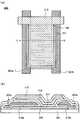
이 실시형태에 있어서, 실시형태 1에서 기술된 트랜지스터(100)의 구조와는 부분적으로 다른 구조를 갖는 트랜지스터(200)가 도 2a 및 도 2b를 참조하여 기술될 것이다.In this embodiment, a
도 2a는 트랜지스터(200)의 상면도이고, 도 2b는 도 2a의 점선 C-D를 따라 취해진 단면도에 해당한다.FIG. 2A is a top view of the
도 2b에 도시되어 있는 것과 같이, 소스 전극층(103)이 기판(101) 위에 제공되고, 게이트 절연층들(210a, 210b) 및 게이트 전극층들(207a, 207b)이 소스 전극층(103) 위에 제공된다. 게이트 절연층들(210a, 210b)은 게이트 전극층들(207a, 207b)의 상면들 및 하면들을 덮고 소스 전극층(103)과 접한다. 또한, 게이트 절연층들(210a, 210b)의 일부들을 덮고 전극층(103)의 일부와 접하도록 산화물 반도체층(211)이 제공된다. 또한, 드레인 전극층(113)이 산화물 반도체층(211) 상에서 그와 접하여 제공되고, 보호 절연층(115)이 드레인 전극층(113) 상에서 그와 접하여 제공된다.As shown in FIG. 2B, a
트랜지스터(200)는, 게이트 전극층(207a) 및 게이트 전극층(207b)이 산화물 반도체층(211)을 개재하여 대향하고 게이트 절연층(210a) 및 게이트 절연층(210b)이 산화물 반도체층(211)을 개재하여 대향하는, 즉, 게이트 전극층들 사이 및 게이트 절연층들 사이에 산화물 반도체층(211)을 개재하여 한 쌍의 게이트 전극층들 및 한 쌍의 게이트 절연층들이 제공된다는 점에서 실시형태 1의 트랜지스터(100)와는 다르다.In the
트랜지스터(200)에 있어서, 게이트 전극층들(207a, 207b)의 일부분들은 소스 전극층(103) 및 드레인 전극층(113)과 중첩하고 게이트 절연층들(210a, 210b)을 개재하여 산화물 반도체층(211)으로 덮인다.In the
또한, 트랜지스터(200)의 산화물 반도체층(211)은 산화물 반도체층(111)과 동일한 재료를 사용하여 형성되고; 따라서, 산화물 반도체층(211)은 고순도화된 산화물 반도체층이 되고 결함 준위들이 감소되는 산화물 반도체층이다.In addition, the
트랜지스터(200)에 있어서, 게이트 전극층들(207a, 207b)의 적어도 일부분들은 산화물 반도체층(211)으로 덮이고, 산화물 반도체층(211)에 충분히 높은 전계가 인가될 수 있고; 따라서, 산화물 반도체층(211)의 넓은 면적에 채널 영역이 형성된다. 따라서, 트랜지스터(200)를 통해 큰 드레인 전류가 흐를 수 있다.In the
또한, 산화물 반도체층(211)의 두께를 크게 함으로써, 트랜지스터(200)는 고 전력 응용을 위한 반도체 장치에 필요한 드레인-파괴-전압 특성들을 가질 수 있다. 또한, 게이트 전극층들(207a, 207b) 및 게이트 절연층들(210a, 210b)은 각각 산화물 반도체층(211)의 넓은 면적에 충분히 높은 전계를 인가하기 위해서 콤형(comb shape)을 갖는 것이 바람직하다.In addition, by increasing the thickness of the
또한, 이 실시형태에서 기술되는 산화물 반도체층(211)은 고순도화된 산화물 반도체층이고; 따라서, 트랜지스터(200)는 오프-상태-전류 특성들이 우수한 트랜지스터일 수 있다.In addition, the
이 실시형태에서 기술되는 기판(101), 소스 전극층(103), 게이트 절연층들(210a, 210b), 게이트 전극층들(207a, 207b), 산화물 반도체층(211), 및 드레인 전극층(113)은 실시형태 1과 유사한 재료들을 사용하여 형성될 수 있다.The
이 실시형태는 임의의 다른 실시형태들에서 기술되는 구성과 적절히 조합하여 구현될 수 있다.This embodiment may be implemented in appropriate combination with the configuration described in any other embodiments.
(실시형태 3)(Embodiment 3)
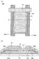
이 실시형태에 있어서, 실시형태 2에서 기술된 트랜지스터(200)의 구조와는 부분적으로 다른 구조를 갖는 트랜지스터(300)가 도 3a 및 도 3b를 참조하여 기술될 것이다.In this embodiment, a
도 3a는 트랜지스터(300)의 상면도이고, 도 3b는 도 3a의 점선 E-F를 따라 취해진 단면도에 해당한다.3A is a top view of the
도 3b에 도시되어 있는 것과 같이, 소스 전극층(103)이 기판(101) 위에 제공되고, 산화물 반도체층(311), 게이트 절연층들(310a, 310b) 및 게이트 전극층들(307a, 307b)이 소스 전극층(103) 위에 제공된다. 게이트 절연층들(310a, 310b)은 게이트 전극층들(307a, 307b)의 상면들 및 하면들을 덮는다. 산화물 반도체층(311)은 소스 전극층(103)과 접한다. 게이트 절연층들(310a, 310b) 및 소스 전극층(103)과 중첩하는 게이트 전극층들(307a, 307b)의 일부분들은 산화물 반도체층(311)으로 덮인다. 또한, 드레인 전극층(113)이 산화물 반도체층(311) 위에 제공되고, 보호 절연층(115)이 드레인 전극층(113) 위에 제공된다.As shown in FIG. 3B, a
트랜지스터(300)는, 게이트 전극층(307a) 및 게이트 절연층(310a)이 게이트 전극층(307b) 및 게이트 절연층(310b)과 대향하고, 산화물 반도체층(311)은 게이트 전극층(307a)과 게이트 전극층(307b) 사이 및 게이트 절연층(310a)과 게이트 절연층(310b) 사이에 제공되고, 즉, 한 쌍의 게이트 전극층들(307a, 307b)이 산화물 반도체층(311)을 개재하여 제공되고 한 쌍의 게이트 절연층들(310a, 310b)이 산화물 반도체층(311)을 개재하여 제공되는 방식으로 형성된다.In the
트랜지스터(300)에 있어서, 소스 전극층(103)과 중첩하는, 게이트 절연층들(310a, 310b) 및 게이트 전극층들(307a, 307b)의 일부분들은 산화물 반도체층(311)으로 덮인다.In the
또한, 트랜지스터(300)의 산화물 반도체층(311)은 산화물 반도체층(111)과 동일한 재료를 사용하여 형성되고; 따라서, 산화물 반도체층(311)은 고순도화된 산화물 반도체층이고 결함 준위들이 감소된 산화물 반도체층이다.In addition, the
트랜지스터(300)에 있어서, 게이트 전극층들(307a, 307b)의 일부분들은 산화물 반도체층(311)으로 덮이고, 산화물 반도체층(311)에 충분한 고 전계가 인가될 수 있으며; 따라서, 산화물 반도체층(311)의 넓은 면적에 채널 영역이 형성된다. 따라서, 트랜지스터(300)를 통해 큰 드레인 전류가 흐를 수 있다.In the
또한, 산화물 반도체층(311)의 두께를 크게 함으로써, 트랜지스터(300)는 고 전력 응용을 위한 반도체 장치에 필요한 드레인-파괴-전압 특성들을 가질 수 있다. 또한, 게이트 전극층들(307a, 307b) 및 게이트 절연층들(310a, 310b) 각각은 산화물 반도체층(311)의 넓은 면적에 충분히 높은 전계를 인가하기 위해서 콤형을 갖는 것이 바람직하다.In addition, by increasing the thickness of the
또한, 이 실시형태에서 기술되는 산화물 반도체층(311)은 고순도화된 산화물 반도체층이고; 따라서, 트랜지스터(300)는 오프-상태-전류 특성들이 우수한 트랜지스터일 수 있다.In addition, the
이 실시형태에서 기술되는 기판(101), 소스 전극층(103), 게이트 절연층들(310a, 310b), 게이트 전극층들(307a, 307b), 및 드레인 전극층(113)은 실시형태 1과 유사한 재료들을 사용하여 형성될 수 있다.The
이 실시형태는 임의의 다른 실시형태들에서 기술되는 구성과 적절히 조합하여 구현될 수 있다.This embodiment may be implemented in appropriate combination with the configuration described in any other embodiments.
(실시형태 4)(Fourth Embodiment)
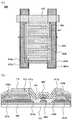
이 실시형태에 있어서, 복수의 유닛들로서, 이들 각각에서 산화물 반도체층을 개재하여 한 쌍의 게이트 전극층들이 대향하고 있고 산화물 반도체층을 개재하여 한 쌍의 게이트 절연층들이 대향하고 있는, 상기 복수의 유닛들을 갖는 트랜지스터가 기술될 것이다. 예로서, 각각의 유닛에서 산화물 반도체층을 개재하여 한 쌍의 게이트 전극층들이 대향하고 있고 산화물 반도체층을 개재하여 한 쌍의 게이트 절연층들이 대향하고 있는, 2개의 유닛을 갖는 트랜지스터(400)가 도 4a 및 도 4b를 참조하여 기술될 것이다.In this embodiment, a plurality of units, each of which a pair of gate electrode layers facing each other via an oxide semiconductor layer and a pair of gate insulating layers facing each other via an oxide semiconductor layer Transistors will be described. By way of example, a
도 4a는 트랜지스터(400)의 상면도이고, 도 4b는 도 4a의 점선 G-H를 따라 취해진 단면도에 해당한다.4A is a top view of
도 4b 및 도 3b에 도시되어 있는 것과 같이, 트랜지스터(400)는, 산화물 반도체층(411)에서, 실시형태 3에서 기술된 트랜지스터(300)에 있어서, 각각의 유닛에서 산화물 반도체층(311)을 개재하여 한 쌍의 게이트 전극층들(307a, 307b)이 대향하고 있고 산화물 반도체층(311)을 개재하여 한 쌍의 게이트 절연층들(310a, 310b)이 대향하고 있는, 2개의 유닛을 갖는 트랜지스터에 대응한다.As shown in FIGS. 4B and 3B, the
큰 드레인 전류에 대한 드레인 파괴 전압을 얻기 위해 트랜지스터(300)의 산화물 반도체층(311)의 두께를 크게 한 경우에, 산화물 반도체층(311)을 개재하여 한 쌍의 게이트 전극층들(307a, 307b)이 대향하고 있고 산화물 반도체층(311)을 개재하여 한 쌍의 게이트 절연층들(310a, 310b)이 대향하고 있는, 하나의 유닛이 사용될 때, 충분히 높은 전계가 산화물 반도체층(311)에 인가될 수 없고, 넓은 채널 영역이 형성될 수 없다. 결과적으로, 큰 드레인 전류를 얻을 수 없을 가능성이 있다.When the thickness of the
따라서, 이 실시형태에서 기술되는 트랜지스터(400)는, 각각의 유닛에서 산화물 반도체층(411)을 개재하여 한 쌍의 게이트 전극층들이 대향하고 있고 산화물 반도체층(411)을 개재하여 한 쌍의 게이트 절연층들이 대향하고 있는, 2개의 유닛을 갖는다. 따라서, 채널 영역인 산화물 반도체층(411)의 두께가 커질 때에도, 충분히 높은 전계가 산화물 반도체층(411)에 인가될 수 있고 넓은 채널 영역이 형성될 수 있음으로써, 큰 드레인 전류가 얻어질 수 있다.Therefore, the
다시 말해서, 트랜지스터(400)에 있어서, 소스 전극층(103)이 기판(101) 위에 제공되고, 산화물 반도체층(411)은 소스 전극층(103)과 접하도록 제공된다. 또한, 산화물 반도체층(411)과 대향하는 한 쌍의 게이트 전극층들(407a, 407b) 및 산화물 반도체층(411)을 개재하여 대향하는 한 쌍의 게이트 절연층들(410a, 410b)의 일부분들 및 산화물 반도체층(411)을 개재하여 대향하는 한 쌍의 게이트 전극층들(415a, 415b) 및 산화물 반도체층(411)을 개재하여 대향하는 한 쌍의 게이트 절연층들(417a, 417b)의 일부분들이 있고; 소스 전극층(103)과 중첩하는 이들 부분들은 산화물 반도체층(411)으로 덮인다. 게이트 절연층들(410a, 410b)은 게이트 전극층들(407a, 407b)의 상면들 및 하면들을 덮는다는 것을 유념해야 한다. 게이트 절연층들(417a, 417b)은 게이트 전극층들(415a, 415b)의 상면들 및 하면들을 덮는다. 또한, 드레인 전극층(113)이 산화물 반도체층(411) 위에 제공되고, 보호 절연층(115)이 드레인 전극층(113) 위에 제공된다.In other words, in the
트랜지스터(400)는 각각의 유닛에서 산화물 반도체층(411)을 개재하여 한 쌍의 게이트 전극층들이 대향하고 있고 산화물 반도체층(411)을 개재하여 한 쌍의 게이트 절연층들이 대향하고 있는, 2개의 유닛을 갖는다.The
트랜지스터(400)에 있어서, 게이트 전극층들(407a, 407b), 게이트 절연층들(410a, 410b), 게이트 전극층들(415a, 415b) 및 게이트 절연층들(417a, 417b)의 소스 전극층(103) 및 드레인 전극층(113)과 중첩하는 부분들은 산화물 반도체층(411)으로 덮인다.In the
또한, 트랜지스터(400)의 산화물 반도체층(411)은 산화물 반도체층(111)과 동일한 재료를 사용하여 형성되고; 따라서, 산화물 반도체층(411)은 고순도화된 산화물 반도체층이고 결함 준위들이 감소된 산화물 반도체층이다.In addition, the
트랜지스터(400)에 있어서, 게이트 전극층들(407a, 407b, 415a, 415b)의 일부분들은 산화물 반도체층(411)으로 덮이고, 충분히 높은 전계가 산화물 반도체층(411)에 인가될 수 있으며; 따라서, 산화물 반도체층(411)의 넓은 면적에 채널 영역이 형성된다. 따라서, 트랜지스터(400)를 통해 큰 드레인 전류가 흐를 수 있다.In the
또한, 산화물 반도체층(411)의 두께를 크게 함으로써, 트랜지스터(400)는 고 전력 응용을 위한 반도체 장치에 필요한 드레인-파괴-전압 특성들을 가질 수 있다. 또한, 게이트 전극층들(407a, 407b), 게이트 절연층들(410a, 410b), 게이트 전극층들(415a, 415b), 및 게이트 절연층들(417a, 417b)은 각각 산화물 반도체층(411)의 넓은 면적에 충분히 높은 전계를 인가하기 위해서 콤형을 갖는 것이 바람직하다.In addition, by increasing the thickness of the
또한, 이 실시형태에서 기술되는 산화물 반도체층(411)은 고순도화된 산화물 반도체층이고; 따라서, 트랜지스터(400)는 오프-상태-전류 특성들이 우수한 트랜지스터가 될 수 있다.In addition, the
이 실시형태에서 기술되는 기판(101), 소스 전극층(103), 게이트 절연층들(410a, 410b, 417a, 417b), 게이트 전극층들(407a, 407b, 415a, 415b), 및 드레인 전극층(113)은 실시형태 1과 유사한 재료들을 사용하여 형성될 수 있다.The
이 실시형태에서는, 각각의 유닛에서 산화물 반도체층을 개재하여 한 쌍의 게이트 전극층들이 대향하고 있고 산화물 반도체층을 개재하여 한 쌍의 게이트 절연층들이 대향하고 있는, 2개의 유닛을 사용하는 실시형태가 기술되지만, 산화물 반도체층을 개재하여 대향하는 게이트 전극층들의 쌍들의 수 및 산화물 반도체층을 개재하여 대향하는 게이트 절연층들의 쌍들의 수에는 특별한 제한이 없고, 그 쌍들의 수는 충분히 높은 전계가 산화물 반도체층에 인가되도록 산화물 반도체층의 두께에 따라 적절히 결정될 수 있다.In this embodiment, an embodiment using two units in which each pair of gate electrode layers face each other via an oxide semiconductor layer and the pair of gate insulating layers face each other via an oxide semiconductor layer is described. Although described, there is no particular limitation on the number of pairs of gate electrode layers opposing through the oxide semiconductor layer and the number of pairs of gate insulating layers opposing through the oxide semiconductor layer, and the number of pairs is sufficiently high. It may be appropriately determined according to the thickness of the oxide semiconductor layer to be applied to the layer.
이 실시형태는 임의의 다른 실시형태들에서 기술되는 구성과 적절히 조합하여 구현될 수 있다.This embodiment may be implemented in appropriate combination with the configuration described in any other embodiments.
(실시형태 5)(Embodiment 5)
이 실시형태에 있어서, 산화물 반도체층을 개재하여 대향하는 한 쌍의 게이트 전극층들 사이 및 산화물 반도체층을 개재하여 대향하는 한 쌍의 게이트 절연층들 사이에 산화물 반도체층으로 덮이는 도전층이 제공되는 구조를 갖는 트랜지스터(500)가 도 5a 및 도 5b를 참조하여 기술될 것이다. 또한, 복수의 유닛들로서, 이들 각각에서 상기 한 쌍의 게이트 전극층들이 대향하고 있고 상기 한 쌍의 게이트 절연층들이 대향하고 있는, 상기 복수의 유닛들이 제공되고 산화물 반도체층으로 덮이는 도전층이 한 쌍의 게이트 전극층들 사이 및 한 쌍의 게이트 절연층들 사이에 제공되는 구조를 갖는 트랜지스터가 기술될 것이다. 예로서, 각각의 유닛에서 상기 한 쌍의 게이트 전극층들이 대향하고 있고 상기 한 쌍의 게이트 절연층들이 대향하고 있는, 2개의 유닛들이 제공되고 산화물 반도체층으로 덮이는 도전층이 한 쌍의 게이트 전극층들 사이 및 한 쌍의 게이트 절연층들 사이에 제공되는 구조를 갖는 트랜지스터(600)가 도 6a 및 도 6b를 참조하여 기술될 것이다.In this embodiment, a conductive layer covered with an oxide semiconductor layer is provided between a pair of gate electrode layers that face each other via an oxide semiconductor layer and between a pair of gate insulating layers that face each other via an oxide semiconductor layer.
도 5a는 트랜지스터(500)의 상면도이고, 도 5b는 도 5a의 점선 I-J를 따라 취해진 단면도에 해당한다. 트랜지스터(500)가 기술될 때, 트랜지스터(300)와 동일한 부분들은 트랜지스터(300)의 설명에서 사용된 공통 참조부호들로 표기된다는 것을 유념해야 한다.5A is a top view of
도 5b 및 도 3b에 도시되어 있는 것과 같이, 트랜지스터(500)에 있어서는, 실시형태 3에서 기술된 트랜지스터(300)에서, 산화물 반도체층(311)을 개재하여 대향하는 한 쌍의 게이트 전극층들(307a, 307b) 사이 및 산화물 반도체층(311)을 개재하여 대향하는 한 쌍의 게이트 절연층들(310a, 310b) 사이에 산화물 반도체층(311)으로 덮이는 도전층(520)이 제공된다. 트랜지스터(500)의 다른 구조들은 트랜지스터(300)와 동일하다.As shown in FIGS. 5B and 3B, in the
트랜지스터(300)에서 채널 영역인 산화물 반도체층(311)이 두껍게 형성되는 경우에, 산화물 반도체층(311)은 응력에 의해 박리될 수 있다. 또한, 트랜지스터(300)의 적층 구조에서 산화물 반도체층(311)의 두꺼운 부분에 변형(오목부)이 발생됨으로써, 산화물 반도체층(311)이 박리될 수 있다.When the
따라서, 이 실시형태에서와 같이, 산화물 반도체층(311)을 개재하여 대향하는 한 쌍의 게이트 전극층들(307a, 307b) 사이 및 산화물 반도체층(311)을 개재하여 대향하는 한 쌍의 게이트 절연층들(310a, 310b) 사이에 산화물 반도체층(311)으로 덮이는 도전층(520)이 형성된다. 따라서, 채널 영역인 산화물 반도체층(311)이 두껍게 형성되는 경우에도, 산화물 반도체층(311)의 응력이 완화됨으로써, 산화물 반도체층(311)의 박리가 방지될 수 있다. 또한, 산화물 반도체층(311)의 두꺼운 부분에 형성된 변형(오목부)이 완화되고, 트랜지스터(300)의 적층 구조는 평탄한 형상에 가깝게 된다. 따라서, 산화물 반도체층(311)의 박리가 방지될 수 있다.Thus, as in this embodiment, between the pair of
도전층(520)은 실시형태 1에서 기술된 소스 전극층(103), 게이트 전극층(107), 또는 드레인 전극층(113)과 유사한 재료를 사용하여 형성될 수 있다. 또한, 도전층(520)은 대향하는 한 쌍의 게이트 전극층들(307a, 307b)이 형성되는 것과 동시에 형성된다.The
다음에, 각각의 유닛에서 산화물 반도체층을 개재하여 한 쌍의 게이트 전극층들이 대향하고 있고 산화물 반도체층을 개재하여 한 쌍의 게이트 절연층들이 대향하고 있는, 2개의 유닛이 제공되고 산화물 반도체층으로 덮이도록 형성되는 도전층들이 한 쌍의 게이트 전극층들 및 한 쌍의 게이트 절연층들이 제공되는 각각의 유닛에 제공되는 구조를 갖는 트랜지스터(600)가 도 6a 및 도 6b를 참조하여 기술될 것이다.Next, in each unit, two units are provided, in which a pair of gate electrode layers face each other via an oxide semiconductor layer, and a pair of gate insulating layers face each other via an oxide semiconductor layer, and are covered with an oxide semiconductor layer. A
도 6a는 트랜지스터(600)의 상면도이고, 도 6b는 도 6a의 점선 K-L을 따라 취해진 단면도에 해당한다. 트랜지스터(600)가 기술될 때, 트랜지스터(400)와 동일한 부분들은 트랜지스터(400)의 설명시 사용된 공통 참조부호들로 표기된다는 것을 유념해야 한다.FIG. 6A is a top view of
트랜지스터(400)의 채널 영역인 산화물 반도체층(411)이 두껍게 형성되는 경우에, 산화물 반도체층(411)은 응력에 의해 박리될 수 있다. 또한, 트랜지스터(400)의 적층 구조에서 산화물 반도체층(411)의 두꺼운 부분에 변형(오목부)이 발생되어, 드레인 전극층(411)이 박리될 수 있다.When the
따라서, 도 6b에 도시되어 있는 것과 같이, 산화물 반도체층(411)으로 덮이는 도전층(620)은 한 쌍의 게이트 전극층들 및 한 쌍의 게이트 절연층들이 제공되는 유닛에 형성되고, 산화물 반도체층(411)으로 덮이는 도전층(622)은 한 쌍의 게이트 전극층들 및 한 쌍의 게이트 절연층들이 제공되는 유닛에 형성된다. 따라서, 채널 영역인 산화물 반도체층(411)이 두껍게 형성되는 경우에도, 산화물 반도체층(411)의 응력이 완화됨으로써, 산화물 반도체층(411)의 박리가 방지될 수 있다. 또한, 산화물 반도체층(411)의 두꺼운 부분에 형성된 변형(오목부)이 완화되고, 트랜지스터(400)의 적층 구조가 평탄한 형상에 가까워진다. 따라서, 산화물 반도체층(411)의 박리가 방지될 수 있다.Thus, as shown in FIG. 6B, the
도전층(620) 및 도전층(622) 각각은 실시형태 1에서 기술된 소스 전극층(103), 게이트 전극층(107), 또는 드레인 전극층(113)과 유사한 재료를 사용하여 형성될 수 있다. 또한, 도전층(620) 및 도전층(622)은 대향하는 한 쌍의 게이트 전극층들(407a, 407b) 및 대향하는 한 쌍의 게이트 전극층들(415a, 415b)이 형성되는 것과 동시에 형성된다.Each of the
트랜지스터(500)에 있어서, 게이트 전극층들(307a, 307b)의 일부분들은 산화물 반도체층(311)으로 덮이고, 산화물 반도체층(311)에 충분히 높은 전계가 인가될 수 있으며; 따라서, 산화물 반도체층(311)의 넓은 면적에 채널 영역이 형성된다. 따라서, 트랜지스터(500)를 통해 큰 드레인 전류가 흐를 수 있다.In the
트랜지스터(600)에 있어서, 게이트 전극층들(407a, 407b, 415a, 415b)의 일부분들은 산화물 반도체층(411)으로 덮이고, 산화물 반도체층(411)에 충분히 높은 전계가 인가될 수 있으며; 따라서, 산화물 반도체층(411)의 넓은 면적에 채널 영역이 형성된다. 따라서, 트랜지스터(600)를 통해 큰 드레인 전류가 흐를 수 있다.In the
또한, 산화물 반도체층(311)의 두께 및 산화물 반도체층(411)의 두께를 크게 함으로써, 트랜지스터(500) 및 트랜지스터(600)는 고 전력 응용을 위한 반도체 장치에 필요한 드레인-파괴-전압 특성들을 가질 수 있다. 또한, 게이트 전극층들 및 게이트 절연층들 각각은 산화물 반도체층(311) 및 산화물 반도체층(411)의 넓은 면적들에 충분히 높은 전계를 인가하기 위해 콤형을 갖는 것이 바람직하다.In addition, by increasing the thickness of the
이 실시형태는 임의의 다른 실시형태들에서 기술되는 구성과 적절히 조합하여 구현될 수 있다.This embodiment may be implemented in appropriate combination with the configuration described in any other embodiments.
(실시형태 6)(Embodiment 6)
이 실시형태에 있어서, 트랜지스터(700) 및 트랜지스터(800)는 도 7a, 도 7b, 도 8a 및 도 8b를 참조하여 기술될 것이다.In this embodiment,
실시형태 1 내지 실시형태 5에 있어서, 게이트 전극층들 및 게이트 절연층들 각각의 바람직한 형상은 콤형이지만; 게이트 전극층은 도 7a, 도 7b, 도 8a 및 도 8b에 도시되어 있는 것과 같이 산화물 반도체층을 둘러싸는 원형일 수 있다. 또한, 산화물 반도체층이 실시형태 5에서 기술된 두께로 형성되는 경우에 발생되는 (응력에 의한 산화물 반도체층의 두꺼운 부분의 박리와 같은) 영향을 고려하면, 도 8b에 도시되어 있는 것과 같이 원형들을 갖도록 형성되는 게이트 전극층 및 게이트 절연층 내부에 산화물 반도체층으로 덮이는 도전층이 형성될 수 있다. 다시 말해서, 게이트 전극층은 실시형태 1 내지 실시형태 5에서 원형을 가질 수 있다.In Embodiments 1 to 5, preferred shapes of each of the gate electrode layers and the gate insulating layers are comb-shaped; The gate electrode layer may be circular to surround the oxide semiconductor layer as shown in FIGS. 7A, 7B, 8A, and 8B. Also, considering the effects (such as peeling of a thick portion of the oxide semiconductor layer by stress) that occurs when the oxide semiconductor layer is formed to the thickness described in Embodiment 5, the prototypes may be formed as shown in FIG. 8B. A conductive layer covered with an oxide semiconductor layer may be formed in the gate electrode layer and the gate insulating layer that are formed to have the same. In other words, the gate electrode layer may have a circular shape in Embodiments 1-5.
또한, 게이트 전극층 및 게이트 절연층은 산화물 반도체층을 개재하여 한 쌍의 게이트 전극층들이 대향하고 있고 산화물 반도체층을 개재하여 한 쌍의 게이트 절연층들이 대향하고 있는 1개의 유닛으로 제한되지 않는다. 복수의 유닛들이 형성될 수 있으며, 이는 채널 영역인 산화물 반도체층이 두껍게 형성되는 경우에 바람직하고; 따라서, 두꺼운 산화물 반도체층에 충분히 높은 전계가 인가될 수 있다.In addition, the gate electrode layer and the gate insulating layer are not limited to one unit in which a pair of gate electrode layers face each other through an oxide semiconductor layer, and a pair of gate insulating layers face each other through an oxide semiconductor layer. A plurality of units can be formed, which is preferable when the oxide semiconductor layer, which is a channel region, is formed thick; Thus, a sufficiently high electric field can be applied to the thick oxide semiconductor layer.
먼저, 예로서, 원형들을 갖도록 형성되는 1개의 게이트 전극층 및 1개의 게이트 절연층이 제공되고 게이트 전극층 및 게이트 절연층의 상면들 및 하면들이 산화물 반도체층으로 덮이는 트랜지스터(700)가 기술될 것이다.First, as an example, a
도 7a는 트랜지스터(700)의 상면도이고, 도 7b는 도 7a의 점선 M-N을 따라 취해진 단면도에 해당한다.FIG. 7A is a top view of the
다시 말해서, 이 실시형태에서 기술되는 도 7b의 트랜지스터에 있어서, 소스 전극층(103)이 기판(101) 위에 형성되고, 산화물 반도체층(711)이 소스 전극층(103)과 접하여 제공된다. 게이트 전극층(707) 및 게이트 절연층(710)은 산화물 반도체층(711)을 둘러싸기 위해 원형들을 갖도록 형성되고, 산화물 반도체층(711)은 게이트 전극층(707)의 상면 및 하면을 덮는 게이트 절연층(710)과 접한다. 또한, 드레인 전극층(113)이 산화물 반도체층(711) 위에 제공된다. 트랜지스터(700)에 있어서, 소스 전극층(103) 및 드레인 전극층(113)과 중첩하는 게이트 전극층(707) 및 게이트 절연층(710)의 일부가, 실시형태 1 내지 실시형태 5에서 기술된 트랜지스터들과 유사한 방식으로 산화물 반도체층(711)에 임베딩된다.In other words, in the transistor of FIG. 7B described in this embodiment, the
다음에, 도 8a는 트랜지스터(800)의 상면도이고, 도 8b는 도 8a의 점선 O-P를 따라 취해진 단면도에 해당한다.Next, FIG. 8A is a top view of the
이 실시형태에서 기술되는 도 8a 및 도 8b의 트랜지스터(800)로서, 트랜지스터(700)에 대한 산화물 반도체층(711)을 둘러싸도록 원형들로 형성되는 게이트 전극층(707) 및 게이트 절연층(710) 내부에 도전층(820)이 제공된다. 트랜지스터(800)에 있어서, 트랜지스터(700)에 도전층(820)을 제공하는 효과는, 실시형태 5에서 기술된, 도전층(520), 도전층(620) 및 도전층(622)을 제공하는 효과와 유사하다.8A and 8B described in this embodiment, the
또한, 트랜지스터(700) 및 트랜지스터(800) 각각에 있어서의 기판(101), 소스 전극층(103), 산화물 반도체층(711), 게이트 전극층(707), 게이트 절연층(710), 및 드레인 전극층(113)은 실시형태 1에서 기술된 재료들을 사용하여 형성될 수 있다. 또한, 트랜지스터(800)의 도전층(820)은 게이트 전극층(707)이 형성되는 것과 동시에 형성되고; 따라서, 도전층(820)은 게이트 전극층(707)과 동일한 재료를 사용하여 형성된다.The
트랜지스터(700) 및 트랜지스터(800)에 있어서, 게이트 전극층(707)의 일부가 산화물 반도체층(711)으로 덮이고, 산화물 반도체층(711)에 충분히 높은 전계가 인가될 수 있으며; 따라서, 산화물 반도체층(711)의 넓은 면적에 채널 영역이 형성된다. 따라서, 트랜지스터(700)를 통해 큰 드레인 전류가 흐를 수 있다.In the
또한, 산화물 반도체층(711)의 두께를 크게 함으로써, 트랜지스터(700) 및 트랜지스터(800)는 고 전력 응용을 위한 반도체 장치에 필요한 드레인-파괴-전압 특성들을 가질 수 있다.In addition, by increasing the thickness of the
이 실시형태는 임의의 다른 실시형태들에서 기술되는 구성과 적절히 조합하여 구현될 수 있다.This embodiment may be implemented in appropriate combination with the configuration described in any other embodiments.
(실시형태 7)(Seventh Embodiment)
이 실시형태에서는, 트랜지스터(100) 및 트랜지스터(200)를 제작하기 위한 방법들이 기술될 것이다. 먼저, 트랜지스터(100)를 제작하기 위한 방법이 도 9a 내지 도 9c를 참조하여 기술될 것이다.In this embodiment, methods for fabricating
하지 절연층이 기판(101) 위에 형성된다. 이 공정을 통해, 유리 기판의 불순물들이 형성될 트랜지스터들로 혼입되는 것이 방지될 수 있다. 편의상, 하지 절연층은 도 9a 내지 도 9c에 도시되어 있지 않다는 것을 유념해야 한다.An underlying insulating layer is formed on the
하지 절연층은 스퍼터링 방법, CVD 방법, 코팅 방법 등에 의해 형성될 수 있다.The underlying insulating layer may be formed by a sputtering method, a CVD method, a coating method, or the like.
하지 절연층이 스퍼터링 방법에 의해 형성될 때, 하지 절연층은 처리실에 남아있는 수소, 물, 수산기, 수소화물 등을 제거하면서 형성되는 것이 바람직하다는 것을 유념해야 한다. 이것은 수소, 물, 수산기, 수소화물 등이 하지 절연층에 함유되는 것을 방지하기 위한 것이다. 처리실에 남아있는 수소, 물, 수산기, 수소화물 등을 제거하기 위해서 흡착형 진공 펌프를 사용하는 것이 바람직하다. 흡착형 진공 펌프로서, 예를 들어, 크라이오펌프, 이온 펌프, 티타늄 서블리메이션 펌프가 사용되는 것이 바람직하다. 배기 수단은 콜드 트랩이 구비된 터보 펌프일 수 있다. 크라이오펌프에 의해 배기된 처리실에서 수소, 물, 수산기, 수소화물 등이 제거되고; 따라서, 하지 절연층이 처리실에서 형성될 때, 하지 절연층에 함유되는 불순물들의 농도가 감소될 수 있다.When the underlying insulating layer is formed by the sputtering method, it should be noted that the underlying insulating layer is preferably formed while removing hydrogen, water, hydroxyl, hydride and the like remaining in the process chamber. This is to prevent hydrogen, water, hydroxyl groups, hydrides, and the like from being contained in the underlying insulating layer. It is preferable to use an adsorption type vacuum pump to remove hydrogen, water, hydroxyl groups, hydrides, and the like remaining in the processing chamber. As the adsorption type vacuum pump, for example, a cryopump, an ion pump, a titanium servation pump is preferably used. The evacuation means may be a turbo pump with a cold trap. Hydrogen, water, hydroxyl groups, hydrides and the like are removed from the treatment chamber exhausted by the cryopump; Therefore, when the underlying insulating layer is formed in the processing chamber, the concentration of impurities contained in the underlying insulating layer can be reduced.
하지 절연층을 형성하기 위해 사용되는 스퍼터링 가스로서, 수소, 물, 수산기 또는 수소화물과 같은 불순물들이, 불순물 농도가 "ppm" 또는 "ppb" 단위로 표현되는 수준으로 감소되는 고순도 가스가 사용되는 것이 바람직하다.As the sputtering gas used to form the underlying insulating layer, it is preferable that a high purity gas is used in which impurities such as hydrogen, water, hydroxyl groups or hydrides are reduced to a level where impurity concentrations are expressed in units of "ppm" or "ppb". desirable.
이 실시형태에 있어서, 기판(101)이 처리실에 도입되고, 수소, 물, 수산기, 수소화물 등이 제거된 고순도 산소를 함유하는 스퍼터링 가스가 처리실에 도입되고, 실리콘 타겟이 사용되는 방식으로 기판(101) 위에 하지 절연층으로서 산화실리콘막이 형성된다. 하지 절연층이 형성될 때, 기판(101)이 가열될 수 있다는 것을 유념해야 한다.In this embodiment, the
하지 절연층이 적층 구조를 사용하여 형성될 때, 예를 들어, 실리콘 타겟 및 수소, 물, 수산기, 수소화물 등이 제거된 고순도 질소를 함유하는 스퍼터링 가스를 사용하여, 산화실리콘막 및 기판 사이에 질화실리콘막이 형성된다. 또한, 이 경우에, 처리실에 남아있는 수소, 물, 수산기, 수소화물 등을 제거하면서 산화실리콘막의 경우와 유사한 방식으로 질화실리콘막이 형성되는 것이 바람직하다. 이 공정에서, 기판(101)이 가열될 수 있다는 것을 유념해야 한다.When the underlying insulating layer is formed using a laminated structure, for example, between the silicon oxide film and the substrate, using a silicon target and a sputtering gas containing high purity nitrogen from which hydrogen, water, hydroxyl groups, hydrides, etc. have been removed, A silicon nitride film is formed. Also in this case, it is preferable that the silicon nitride film is formed in a similar manner to that of the silicon oxide film while removing hydrogen, water, hydroxyl groups, hydride and the like remaining in the processing chamber. It should be noted that in this process, the
질화실리콘막 및 산화실리콘막이 하지 절연층으로서 적층되는 경우에, 질화실리콘막 및 산화실리콘막은 공통 실리콘 타겟을 사용하여 동일한 처리실에서 형성될 수 있다. 먼저, 질소를 함유하는 스퍼터링 가스가 도입되고 처리실에 장착된 실리콘 타겟이 사용되는 방식으로 질화실리콘막이 형성된다. 이어서, 가스가 산소를 함유하는 스퍼터링 가스로 전환되고 동일한 실리콘 타겟이 사용되는 방식으로 산화실리콘막이 형성된다. 질화실리콘막 및 산화실리콘막은 대기에 노출되지 않고 연속하여 형성될 수 있고; 따라서, 수소, 물, 수산기 또는 수소화물과 같은 불순물들이 질화실리콘막의 표면에 부착되는 것이 방지될 수 있다.In the case where the silicon nitride film and the silicon oxide film are laminated as the underlying insulating layer, the silicon nitride film and the silicon oxide film can be formed in the same process chamber using a common silicon target. First, a silicon nitride film is formed in such a manner that a sputtering gas containing nitrogen is introduced and a silicon target mounted in the processing chamber is used. Then, the silicon oxide film is formed in such a manner that the gas is converted to oxygen-containing sputtering gas and the same silicon target is used. The silicon nitride film and the silicon oxide film can be formed continuously without being exposed to the atmosphere; Thus, impurities such as hydrogen, water, hydroxyl groups or hydrides can be prevented from adhering to the surface of the silicon nitride film.
이어서, 소스 전극층(103)이 하지 절연층 위에 형성된다. 먼저, 물리 증착 방법(PVD 방법)인 스퍼터링 방법, 화학 증착 방법(CVD 방법) 또는 진공 증착 방법에 의해 도전막이 기판(101) 위에 형성된다. 제 1 포토리소그래피 단계에서 레지스트 마스크가 도전막 위에 형성되고, 레지스트 마스크를 사용하여 도전막에 대해 제 1 에칭 처리가 수행됨으로써, 소스 전극층(103)이 형성된다. 대안적으로, 소스 전극층(103)은 포토리소그래피 단계를 사용하지 않고 프린팅 방법 또는 잉크-젯 방법에 의해 형성되어, 단계들의 수가 감소될 수 있다. 나중에 형성되는 게이트 절연층과의 커버리지가 향상될 수 있기 때문에, 소스 전극층(103)의 종단부들은 테이퍼형인 것이 바람직하다는 것을 유념해야 한다.Subsequently, a
이 실시형태에 있어서, 소스 전극층(103)이 되는 도전막으로서, 50㎚ 두께의 티타늄막, 100㎚ 두께의 알루미늄막 및 50㎚ 두께의 티타늄막이 스퍼터링 방법에 의해 순서대로 적층되고, 제 1 포토리소그래피 단계에서 형성된 레지스트 마스크를 사용하여 제 1 에칭이 수행됨으로써, 소스 전극층(103)이 형성된다.In this embodiment, as the conductive film to be the
다음에, 게이트 절연층(110)이 되는 제 1 절연막(104)이 소스 전극층(103) 위에 형성된다. 게이트 절연층(110)이 되는 제 1 절연막(104)이 스퍼터링 방법에 의해 형성됨으로써, 절연막(104)의 수소 농도가 감소될 수 있다. 스퍼터링 방법에 의해 산화실리콘막을 형성하는 경우에, 타겟으로서 실리콘 타겟 또는 석영 타겟이 사용되고, 산소 또는 산소와 아르곤의 혼합 가스가 스퍼터링 가스로서 사용된다. 제 1 절연막(104)은 수소 농도가 감소되도록 형성되는 것이 바람직하다. 제 1 절연막(104)은 하지 절연층을 형성하기 위한 방법과 유사한 방법을 사용하여 형성될 수 있다. 예를 들어, 제 1 절연막(104)은 수소, 물, 수산기, 수소화물 등이 제거된 고순도 산소를 함유하는 스퍼터링 가스를 사용하여 형성되거나, 또는 제 1 절연막(104)은 처리실에 남아있는 수소, 물, 수산기, 수소화물 등을 제거하면서 형성된다. 또한, 스퍼터링 장치의 내벽, 타겟의 표면 또는 타겟 재료 내부에 남아있는 수분이나 수소를 제거하기 위해서, 제 1 절연막(104)이 형성되기 전에 예열 처리가 수행되는 것이 바람직하다. 예열 처리 후에, 기판 또는 스퍼터링 장치는 냉각된다. 이어서, 제 1 절연막(104)이 대기에 노출되지 않고 형성된다. 이 실시형태에서는, 100㎚의 두께를 갖는 산화실리콘막이 형성된다는 것을 유념해야 한다.Next, a first
제 1 절연막(104)은 적층 구조를 가질 수 있다. 예를 들어, 5㎚ 이상 및 300㎚ 이하의 두께를 갖는 산화실리콘막(SiOx(x>0)) 및 50㎚ 이상 및 200㎚ 이하의 두께를 갖는 질화실리콘막(SiNy(y>0))이 스퍼터링 방법에 의해 산화실리콘막 위에 형성되는 적층 구조가 사용될 수 있다.The first insulating
다음에, 게이트 전극층(107)이 제 1 절연막(104) 위에 형성된다. 게이트 전극층(107)은 소스 전극층(103)과 유사한 방식으로 형성될 수 있다. 먼저, 제 1 절연막(104) 위에 도전막이 형성되고, 제 2 포토리소그래피 단계에서 레지스트 마스크가 형성되고, 레지스트 마스크를 사용하여 도전막에 대해 제 2 에칭이 수행됨으로써, 게이트 전극층(107)이 형성될 수 있다. 이 실시형태에 있어서, 150㎚의 두께를 갖는 티타늄막이 스퍼터링 방법에 의해 형성된 후에, 게이트 전극층(107)이 포토리소그래피 단계 및 에칭 단계에 의해 형성된다. 게이트 전극층(107)을 형성하는 단계를 통해, 게이트 배선 또한 동시에 형성될 수 있다.Next, a
게이트 절연층(110)이 되는 제 2 절연막(106)이 제 1 절연막(104) 및 게이트 전극층(107) 위에 형성된다. 제 2 절연막(106)은 제 1 절연막(104)과 유사한 방식으로 형성될 수 있다. 이 실시형태에서는, 100㎚의 두께를 갖는 산화실리콘막이 스퍼터링 방법에 의해 형성된다. 여기까지의 단계들은 도 9a에 도시되어 있다.The second
다음에, 소스 전극층(103)의 일부를 노출시키기 위해 레지스트 마스크가 제 3 포토리소그래피 단계에서 형성되고, 제 1 절연막(104) 및 제 2 절연막(106)이 레지스트 마스크를 사용하여 에칭됨으로써, 게이트 절연층(110)이 형성된다.Next, a resist mask is formed in the third photolithography step to expose a portion of the
다음에, 게이트 절연층(110) 및 소스 전극층(103)의 일부와 접하게 되는 섬 형상 산화물 반도체층이 형성된다. 이어서, 섬 형상 산화물 반도체층과 접하는 드레인 전극층(113)이 형성된다.Next, an island-shaped oxide semiconductor layer in contact with a portion of the
먼저, 게이트 절연층(110) 및 소스 전극층(103)의 일부 위에 스퍼터링 방법, 코팅 방법, 프린팅 방법 등에 의해 산화물 반도체막이 형성된다. 다음에, 드레인 전극층(113)이 되는 도전막이 산화물 반도체막 위에 형성된다. 이 실시형태에서는, 산화물 반도체막이 스퍼터링 방법에 의해 형성된다.First, an oxide semiconductor film is formed on a part of the
전처리로서, 지금까지의 단계들을 통해 및 도 9a의 단계를 포함하여 형성된 기판(101)은 스퍼터링 장치의 예열실에서 예열되고, 기판(101)에 부착된 수소, 물, 수산기 또는 수소화물과 같은 불순물들이 제거되어, 수소가 산화물 반도체막에 가능한 한 적게 함유되도록 한다. 예열실에 제공되는 배기 수단으로서, 크라이오펌프가 바람직하다. 이 예열 처리는 생략될 수 있다는 것을 유념해야 한다. 이 예열 단계는, 소스 전극층(103)은 형성되지만 게이트 절연층(110)은 형성되지 않는 기판(101) 상에서 수행될 수 있거나, 또는 나중 단계에서 형성되는 드레인 전극층(113)이 형성되지 않는 기판(101)에 대해 수행될 수 있다.As a pretreatment, the
산화물 반도체막이 스퍼터링 방법에 의해 형성되기 전에, 아르곤 가스의 도입에 의해 플라즈마가 발생되는 역 스퍼터링이 수행되는 것이 바람직하고, 게이트 절연층(110) 및 소스 전극층(103) 일부의 표면들에 부착된 입자들 및 산화막이 제거되어, 게이트 절연층(110)과 산화물 반도체막 사이 및 소스 전극층(103)의 일부 및 산화물 반도체막 사이의 계면에서의 저항이 감소될 수 있다는 것을 유념해야 한다. 역 스퍼터링은, 전압을 타겟 측에 인가하지 않고, 아르곤 분위기에서 기판 측에 전압을 인가하기 위해 고주파수 전원이 사용되고 표면을 개질하기 위해 기판 부근에서 플라즈마가 발생되는 방법을 말한다. 아르곤 분위기 대신, 질소 분위기, 헬륨 분위기 등이 사용될 수 있다는 것을 유념해야 한다.Before the oxide semiconductor film is formed by the sputtering method, it is preferable that reverse sputtering in which plasma is generated by introduction of argon gas is performed, and particles adhered to the surfaces of a portion of the
이 실시형태에 있어서, 산화물 반도체 타겟을 사용하여 스퍼터링 방법에 의해 산화물 반도체막이 형성된다. 산화물 반도체막은 희가스(대표적으로, 아르곤) 분위기, 산소 분위기, 또는 희가스(대표적으로, 아르곤)와 산소의 분위기에서 스퍼터링 방법에 의해 형성될 수 있다. 스퍼터링 방법이 이용될 때, 2wt% 내지 10wt%의 SiO2를 함유하는 타겟이 사용될 수 있다.In this embodiment, an oxide semiconductor film is formed by a sputtering method using an oxide semiconductor target. The oxide semiconductor film can be formed by a sputtering method in a rare gas (typically argon) atmosphere, an oxygen atmosphere, or a rare gas (typically argon) and oxygen atmosphere. When the sputtering method is used, a target containing2 wt% to 10 wt% SiO2 may be used.
산화물 반도체막을 형성하기 위해 사용되는 스퍼터링 가스로서, 수소, 물, 수산기 또는 수소화물과 같은 불순물들이, 불순물 농도가 "ppm" 또는 "ppb" 단위로 표현되는 레벨로 감소되는 고순도 가스가 사용되는 것이 바람직하다.As the sputtering gas used to form the oxide semiconductor film, it is preferable to use a high purity gas in which impurities such as hydrogen, water, hydroxyl groups or hydrides are reduced to a level in which the impurity concentration is expressed in units of "ppm" or "ppb". Do.
이 실시형태에서 사용되는 산화물 반도체 타겟의 예로서, In, Ga 및 Zn을 함유하는 산화물 반도체 타겟(조성비는 In2O3:Ga2O3:ZnO=1:1:1[몰비], 즉, In:Ga:Zn=1:1:0.5[몰비])이 사용될 수 있다. In, Ga 및 Zn을 함유하는 산화물 반도체 타겟으로서, In:Ga:Zn=1:1:1[몰비] 또는 In:Ga:Zn=1:1:2[몰비]의 조성비를 갖는 타겟이 사용될 수 있다. 산화물 반도체 타겟의 충전율은 90% 이상 및 100% 이하, 바람직하게, 95% 이상 및 99.9% 이하이다. 충전율이 높은 산화물 반도체 타겟을 사용하여 형성되는 산화물 반도체막은 조밀하다.As an example of the oxide semiconductor target used in this embodiment, an oxide semiconductor target containing In, Ga, and Zn (the composition ratio is In2 O3 : Ga2 O3 : ZnO = 1: 1: 1 [molar ratio], that is, In: Ga: Zn = 1: 1: 0.5 [molar ratio]) may be used. As the oxide semiconductor target containing In, Ga and Zn, a target having a composition ratio of In: Ga: Zn = 1: 1: 1 [molar ratio] or In: Ga: Zn = 1: 1: 2 [molar ratio] can be used. have. The filling rate of the oxide semiconductor target is at least 90% and at most 100%, preferably at least 95% and at most 99.9%. The oxide semiconductor film formed using the oxide semiconductor target with a high filling rate is dense.
산화물 반도체로서 In-Zn-O계 재료가 사용되는 경우에, 타겟은 원자비로 In:Zn=50:1 내지 1:2(몰비로 In2O3:ZnO=25:1 내지 1:4), 바람직하게, 원자비로 In:Zn=20:1 내지 1:1(몰비로 In2O3:ZnO=10:1 내지 1:2), 더욱 바람직하게, 원자비로 In:Zn=15:1 내지 1.5:1(몰비로 In2O3:ZnO=15:2 내지 3:4)의 조성비를 갖는다. 예를 들어, In:Zn:O=X:Y:Z의 원자비를 갖는 In-Zn-O계 산화물 반도체를 형성하는데 사용되는 타겟에서,Z>1.5X+Y의 관계가 만족된다.When In-Zn-O based materials are used as the oxide semiconductor, the target is In: Zn = 50: 1 to 1: 2 in atomic ratio (In2 O3 : ZnO = 25: 1 to 1: 4 in molar ratio). , Preferably, In: Zn = 20: 1 to 1: 1 in an atomic ratio (In2 O3 : ZnO = 10: 1 to 1: 2 in a molar ratio), more preferably In: Zn = 15: in an atomic ratio 1 to 1.5: 1 has a composition ratio of (in2 O in a molar ratio3: 4 ZnO = 15:: 2 to 3). For example, in a target used to form an In—Zn—O based oxide semiconductor having an atomic ratio of In: Zn: O =X :Y :Z , the relationship ofZ > 1.5X +Y is satisfied.
감압된 상태로 유지되는 처리실에 기판이 보유되고 처리실에 남아있는 수분이 제거되면서, 수소, 물, 수산기, 수소화물 등이 제거된 스퍼터링 가스가 처리실에 도입되고 금속 산화물이 타겟으로서 사용되는 방식으로, 소스 전극층(103) 및 게이트 절연층(110) 위에 산화물 반도체막이 형성된다. 처리실에 남아있는 수소, 물, 수산기, 수소화물 등을 제거하기 위해서 흡착형 진공 펌프를 사용하는 것이 바람직하다. 예를 들어, 크라이오펌프, 이온 펌프 또는 티타늄 서블리메이션 펌프가 사용되는 것이 바람직하다. 배기 수단은 콜드 트랩이 구비된 터보 펌프일 수 있다. 예를 들어, 수소, 물, 수산기, 수소화물 등(더욱 바람직하게, 탄소 원자를 함유하는 화합물을 포함함)이 크라이오펌프를 사용하여 처리실로부터 배기된다. 따라서, 이 처리실에서 형성된 산화물 반도체막에 함유되는 불순물들의 농도가 감소될 수 있다. 산화물 반도체막은 기판이 가열되는 동안 형성될 수 있다.In such a manner that a sputtering gas from which hydrogen, water, hydroxyl groups, hydrides, and the like have been removed is introduced into the processing chamber and a metal oxide is used as a target while the substrate is held in the processing chamber maintained at a reduced pressure and water remaining in the processing chamber is removed. An oxide semiconductor film is formed on the
이 실시형태에서, 성막 조건의 예로서, 다음 조건들이 적용된다: 기판(101)과 타겟 간의 거리가 170㎜이고; 기판 온도가 250℃이고; 압력이 0.4Pa이고; 직류(DC) 전원이 0.5㎾이고; 분위기가 산소를 함유하거나 분위기가 아르곤을 함유하거나 또는 분위기가 산소와 아르곤을 함유한다. 펄스형 직류(DC) 전원이 사용되는 것이 바람직하고, 그 경우에는 먼지가 감소될 수 있고 두께가 균일하게 될 수 있다는 것을 유념해야 한다. 산화물 반도체막의 두께는 50㎚ 이상 및 500㎚ 이하인 것이 바람직하다. 이 실시형태에서 산화물 반도체막의 두께는 100㎚이다. 산화물 반도체막의 적절한 두께는 산화물 반도체층(111)에 사용되는 산화물 반도체 재료에 따라서 다르고; 따라서, 두께는 산화물 반도체 재료에 따라 적절히 결정될 수 있다는 것을 유념해야 한다.In this embodiment, as an example of deposition conditions, the following conditions apply: the distance between the
드레인 전극층(113)이 되는 도전막이 소스 전극층(103)과 유사한 방식으로 형성될 수 있다. 이 실시형태에서, 드레인 전극층(113)이 되는 도전막으로서, 50㎚ 두께의 티타늄막, 100㎚ 두께의 알루미늄막 및 50㎚ 두께의 티타늄 막이 순서대로 적층된다.The conductive film serving as the
다음에, 제 4 포토리소그래피 단계에서 도전막 위에 레지스트 마스크가 형성되고, 드레인 전극층(113)이 되는 도전막 및 섬 형상 산화물 반도체층이 되는 산화물 반도체막이 레지스트 마스크를 사용하여 에칭됨으로써, 드레인 전극층(113) 및 섬 형상 산화물 반도체층이 형성된다. 제 4 포토리소그래피 단계에서 형성되는 레지스트 마스크 대신 잉크젯 방법을 사용하여 레지스트 마스크를 형성함으로써, 단계들의 수가 감소될 수 있다. 여기서, 도전막 및 산화물 반도체막의 에칭은 드라이 에칭이나 웨트 에칭 중 하나를 사용하거나, 또는 드라이 에칭과 웨트 에칭 모두를 사용하여 수행될 수 있다는 것을 유념해야 한다. (에천트, 에칭 시간, 및 온도와 같은) 에칭 조건들은 소망의 형상들을 갖는 드레인 전극층(113) 및 섬 형상 산화물 반도체층을 형성하기 위해서 재료에 따라 적절히 조정된다. 예를 들어, 도전막은 웨트 에칭에 의해 드레인 전극층(113)으로 가공될 수 있고; 이어서, 마스크로서 드레인 전극층(113)을 사용하여 드라이 에칭에 의해 산화물 반도체막이 섬 형상 산화물 반도체층으로 가공될 수 있다.Next, in the fourth photolithography step, a resist mask is formed over the conductive film, and the conductive film to be the
산화물 반도체막의 웨트 에칭에 사용되는 에천트로서, 인산, 아세트산 및 초산의 혼합 용액, 암모니아 과수(31wt%의 과산화수소수:28wt%의 암모니아수:물=5:2:2(체적비)) 등이 사용될 수 있다. 또한, ITO07N(칸토 케미칼사 제품)이 또한 사용될 수 있다.As the etchant used for the wet etching of the oxide semiconductor film, a mixed solution of phosphoric acid, acetic acid and acetic acid, ammonia per water (31 wt% hydrogen peroxide: 28 wt% aqueous ammonia: water = 5: 2: 2 (volume ratio)) and the like can be used. have. In addition, ITO07N (manufactured by Canto Chemical Co., Ltd.) may also be used.
웨트 에칭 후 에천트는 에칭된 재료들과 함께 세정에 의해 제거된다. 에천트 및 에칭된 재료를 포함하는 폐액은 정제될 수 있고 재료는 재사용될 수 있다. 산화물 반도체막에 함유된 인듐과 같은 재료가 에칭 후 폐액으로부터 수집되어 재사용될 때, 자원들이 효율적으로 사용될 수 있고, 비용이 감소될 수 있다.After the wet etch the etchant is removed by cleaning with the etched materials. Waste fluids comprising etchant and etched material can be purified and the material can be reused. When materials such as indium contained in the oxide semiconductor film are collected from the waste liquid after etching and reused, resources can be used efficiently, and the cost can be reduced.
산화물 반도체막의 드라이 에칭에 사용되는 에칭 가스로서, 염소를 함유하는 가스(염소(Cl2), 삼염화붕소(BCl3), 사염화실리콘(SiCl4), 또는 사염화탄소(CCl4)와 같은 염소계 가스)가 사용되는 것이 바람직하다.As an etching gas used for dry etching of an oxide semiconductor film, a gas containing chlorine (chlorine-based gas such as chlorine (Cl2 ), boron trichloride (BCl3 ), silicon tetrachloride (SiCl4 ), or carbon tetrachloride (CCl4 )) is used. It is preferred to be used.
대안적으로, 불소를 함유하는 가스(사불화탄소(CF4), 육불화황(SF6), 삼불화질소(NF3), 또는 트리플루오로메탄(CHF3)과 같은 불소계 가스); 브롬화수소(HBr); 산소(O2); 헬륨(He) 또는 아르곤(Ar)과 같은 희가스가 첨가된 이들 가스들 중 임의의 가스 등이 사용될 수 있다.Alternatively, a fluorine-containing gas (carbon fluoride (CF4 ), sulfur hexafluoride (SF6 ), nitrogen trifluoride (NF3 ), or fluorine-based gas such as trifluoromethane (CHF3 )); Hydrogen bromide (HBr); Oxygen (O2 ); Any of these gases to which a rare gas such as helium (He) or argon (Ar) is added may be used.
드라이 에칭 방법으로서, 평행평판형 반응성 이온 에칭(RIE) 방법 또는 유도 결합 플라즈마(ICP) 에칭 방법이 사용될 수 있다. 막을 소망의 형상으로 에칭하기 위해서, 에칭 조건들(코일형 전극에 인가되는 전력량, 기판 측 상의 전극에 인가되는 전력량, 기판 측 상의 전극의 온도 등)이 적절히 조정된다.As a dry etching method, a parallel plate type reactive ion etching (RIE) method or an inductively coupled plasma (ICP) etching method can be used. In order to etch the film in a desired shape, etching conditions (the amount of power applied to the coil-type electrode, the amount of power applied to the electrode on the substrate side, the temperature of the electrode on the substrate side, etc.) are appropriately adjusted.
여기까지의 단계들은 도 9b에 도시되어 있다.The steps so far are shown in FIG. 9B.
다음에, 섬 형상 산화물 반도체층에 열 처리가 행해진다. 열 처리의 온도는 400℃ 이상 및 750℃ 이하, 바람직하게, 400℃ 이상 및 기판의 변형점 미만이다. 여기서, 기판은 일종의 열 처리 장치인 전기노에 도입되고, 질소 또는 희가스와 같은 불활성 가스의 분위기에서 1시간 동안 450℃로 섬 형상 산화물 반도체층에 열 처리가 수행된다. 이어서, 산화물 반도체층은 대기에 노출되지 않고; 따라서, 수소, 물, 수산기, 수소화물 등이 섬 형상 산화물 반도체층에 투입되는 것을 방지할 수 있다. 결과적으로, 수소의 농도가 감소된 고순도화된 산화물 반도체층(111)이 얻어질 수 있다. 즉, 섬 형상 산화물 반도체층의 탈수화 및 탈수소화 중 적어도 하나가 열 처리에 의해 수행될 수 있다.Next, heat treatment is performed on the island-shaped oxide semiconductor layer. The temperature of the heat treatment is at least 400 ° C and at most 750 ° C, preferably at least 400 ° C and below the strain point of the substrate. Here, the substrate is introduced into an electric furnace, which is a kind of heat treatment device, and heat treatment is performed on the island-shaped oxide semiconductor layer at 450 ° C. for 1 hour in an atmosphere of an inert gas such as nitrogen or a rare gas. The oxide semiconductor layer is then not exposed to the atmosphere; Therefore, it is possible to prevent hydrogen, water, hydroxyl groups, hydrides, and the like from being introduced into the island oxide semiconductor layer. As a result, a highly purified
열 처리에 있어서, 수소, 물, 수산기, 수소화물 등은 질소 또는 헬륨, 네온이나 아르곤과 같은 희가스에 함유되지 않는 것이 바람직하다는 것을 유념해야 한다. 대안적으로, 열 처리 장치에 도입되는 질소 또는 헬륨, 네온이나 아르곤과 같은 희가스의 순도는 바람직하게 6N(99.9999%) 이상, 더욱 바람직하게, 7N(99.99999%) 이상이다(즉, 불순물들의 농도는 1ppm 이하, 바람직하게, 0.1ppm 이하이다).It should be noted that in the heat treatment, hydrogen, water, hydroxyl groups, hydrides and the like are preferably not contained in nitrogen or in rare gases such as helium, neon or argon. Alternatively, the purity of nitrogen or rare gases such as helium, neon or argon introduced into the heat treatment device is preferably at least 6N (99.9999%), more preferably at least 7N (99.99999%) (ie the concentration of impurities is 1 ppm or less, preferably 0.1 ppm or less).
또한, 섬 형상 산화물 반도체층에 대해 수행되는 열 처리는, 산화물 반도체막 및 드레인 전극층(113)이 되는 도전층에 대해 수행되는 제 4 포토리소그래피 단계 이전에 수행될 수 있다. 그 경우에, 열 처리 후에, 기판이 열 처리 장치에서 꺼내지고 제 4 포토리소그래피 단계가 수행된다. 대안적으로, 열 처리는 드레인 전극층(113)이 되는 도전막이 산화물 반도체막 위에 형성되기 전에 수행될 수 있다.Further, the heat treatment performed on the island-shaped oxide semiconductor layer may be performed before the fourth photolithography step performed on the conductive layer serving as the oxide semiconductor film and the
다음에, 보호 절연층(115)이 형성된다. 보호 절연층(115)은 산화실리콘막, 산화질화실리콘막, 산화알루미늄막, 또는 산화질화알루미늄막과 같은 산화물 절연막; 또는 질화실리콘막, 질화산화실리콘막, 질화알루미늄막 또는 질화산화알루미늄막과 같은 질화물 절연막을 사용하여 형성된다. 대안적으로, 산화물 절연막 및 질화물 절연막이 적층될 수 있다. 보호 절연층(115)은 제 1 절연막(104) 및 제 2 절연막(106)과 유사한 방식으로 형성될 수 있다.Next, a protective
보호 절연층(115)이 형성된 후에, 1시간 이상 및 30시간 이하 동안 대기 중에서 100℃ 이상 및 200℃ 이하에서 열 처리가 수행될 수 있다. 그 경우에, 열 처리는 제 2 열 처리라고 할 수 있고, 탈수화 및 탈수소화 중 적어도 하나가 수행되는 열처리는 제 1 열 처리라고 할 수 있다. 트랜지스터(100)의 신뢰성은 제 2 열 처리에 의해 향상될 수 있다. 여기까지의 단계들은 도 9c에 도시되어 있다.After the protective insulating
상기 공정을 통해, 고순도화되고 수소 농도가 감소된 산화물 반도체층(111)을 포함하는 트랜지스터(100)가 형성될 수 있다. 따라서, 이 실시형태에서 기술된 제작 방법에 의해, 실시형태 1에 기술된 것과 같이 큰 드레인 전류가 흐를 수 있고 드레인-파괴-전압 특성들이 높은 트랜지스터(100)가 형성될 수 있다.Through the above process, the
여기서, 트랜지스터(200)를 제작하기 위한 방법이 도 10a 및 도 10b를 참조하여 기술될 것이다. 트랜지스터(200)로서, 트랜지스터(100)를 제작하기 위한 방법에서, 게이트 전극층(107)이 형성될 때 게이트 전극층들(207a, 207b)로서 작용하는 도전막들이 대향하는 방식으로 포토리소그래피 단계가 수행되고 레지스트 마스크가 형성된다. 도전막이 레지스트 마스크를 사용하여 에칭됨으로써, 대향하는 게이트 전극층들(207a, 207b)이 형성될 수 있다(도 10a 참조).Here, a method for manufacturing the
이어서, 이 실시형태에서 기술된 단계들이 적절히 수행됨으로써, 실시형태 2에서 기술된 트랜지스터(200)가 형성될 수 있다(도 10b 참조).Subsequently, the steps described in this embodiment are appropriately performed, whereby the
이 실시형태는 임의의 다른 실시형태들에서 기술되는 구성과 적절히 조합하여 구현될 수 있다.This embodiment may be implemented in appropriate combination with the configuration described in any other embodiments.
(실시형태 8)(Embodiment 8)
이 실시형태에서, 트랜지스터(300), 트랜지스터(400) 및 트랜지스터(700)를 제작하기 위한 방법들이 기술될 것이다. 먼저, 트랜지스터(300)는 도 11a 내지 도 11d를 참조하여 기술될 것이다.In this embodiment, methods for fabricating
실시형태 7과 유사한 기판이 기판(101)으로서 사용될 수 있다. 이어서, 하지 절연층 및 소스 전극층(103)이 실시형태 7과 유사한 방식으로 형성된다.A substrate similar to Embodiment 7 can be used as the
다음에, 산화물 반도체층(308)이 소스 전극층(103) 위에 형성된다(도 11a 참조).Next, an
산화물 반도체층(308)이 되는 제 1 산화물 반도체막이 실시형태 7과 유사한 방식으로 형성될 수 있다. 여기서, 100㎚의 두께를 갖는 In-Ga-Zn-O계 산화물 반도체막이 소스 전극층(103) 위에 형성된다. 이어서, 포토리소그래피 단계가 수행되고, 제 1 산화물 반도체막이 에칭됨으로써, 산화물 반도체층(308)이 형성된다. 포토리소그래피 단계 및 에칭 단계는 실시형태 7과 유사한 방식으로 수행될 수 있다.The first oxide semiconductor film serving as the
다음에, 게이트 절연층들(310a, 310b)로 덮이고, 대향하는 게이트 전극층들(307a, 307b)이 산화물 반도체층(308) 위에 형성된다. 대향하는 게이트 전극층들(307a, 307b) 및 게이트 절연층들(310a, 310b)은 실시형태 7에서 기술된 방법에 의해 형성될 수 있다(도 11b 참조).Next, covered with the
다음에, 게이트 절연층들(310a, 310b) 및 산화물 반도체층(308)의 일부 위에 제 2 산화물 반도체막이 형성된다. 제 2 산화물 반도체막은 제 1 산화물 반도체막과 유사한 방식으로 형성된다. 이 실시형태에 있어서, In-Ga-Zn-O계 산화물 반도체막은 100㎚로 형성된다. 또한, 드레인 전극층(113)이 되는 도전막이 실시형태 7과 유사한 방식으로 제 2 산화물 반도체막 위에 형성된다. 여기서, 50㎚ 두께의 티타늄막, 100㎚ 두께의 알루미늄막, 및 50㎚ 두께의 티타늄막이 순서대로 적층된다.Next, a second oxide semiconductor film is formed over the
포토리소그래피 단계 및 에칭 단계가 수행된다. 이어서, 탈수화 및 탈수소화 중 적어도 하나가 수행되는 열 처리가 행해짐으로써, 산화물 반도체층(311) 및 드레인 전극층(113)이 형성된다(도 11c 참조). 포토리소그래피 단계 및 에칭 단계는 여기서 실시형태 7에서 기술된 방법에 의해 수행될 수 있다. 이 단계에 의하면, 구조는 산화물 반도체층(311)을 개재하여 대향하는 한 쌍의 게이트 전극층들(307a, 307b) 및 산화물 반도체층(311)을 개재하여 대향하는 한 쌍의 게이트 절연층들(310a, 310b)을 포함하고, 이는 실시형태 3에서 기술된 트랜지스터(300)의 특징이다. 열 처리는 실시형태 7에서 기술된 것과 유사한 방법에 의해 수행될 수 있고, 열 처리 또한 실시형태 7에서 기술된 것과 동일한 타이밍에 수행될 수 있다.A photolithography step and an etching step are performed. Subsequently, a heat treatment is performed in which at least one of dehydration and dehydrogenation is performed, whereby the
다음에, 보호 절연층(115)은 실시형태 7과 유사한 방식으로 형성되고, 또한, 실시형태 7에서 기술된 제 2 열 처리가 적절히 수행됨으로써, 실시형태 3에서 기술된 트랜지스터(300)가 형성될 수 있다(도 11d 참조).Next, the protective insulating
여기서, 실시형태 4에서 기술된 트랜지스터(400)를 제작하기 위한 방법이 도 12a 내지 도 12d를 참조하여 기술될 것이다. 이 실시형태에서 기술된 산화물 반도체층(311)이 형성된 후에(도 12a 참조), 절연막(401) 및 나중에 게이트 전극층들(415a, 415b)로서 작용하게 되는 도전막(403)이 산화물 반도체층(311) 위에 형성된다(도 12b 참조). 이어서, 게이트 전극층들(415a, 415b)이 포토리소그래피 단계 및 에칭 단계를 수행함으로써 형성된다. 그 후에, 게이트 절연층들(417a, 417b)을 덮도록 절연막이 형성되고, 포토리소그래피 단계 및 에칭 단계가 수행됨으로써, 게이트 절연층들(417a, 417b)이 형성될 수 있다(도 12c 참조). 게이트 전극층들(415a, 415b) 및 게이트 절연층들(417a, 417b)의 상세한 설명을 위해서, 실시형태 7에서의 기술을 적절히 참조한다는 것을 유념해야 한다.Here, a method for fabricating the
다음에, 제 3 산화물 반도체막이 산화물 반도체층(311) 위에 형성되고, 포토리소그래피 단계 및 에칭 단계가 수행됨으로써, 산화물 반도체층(411)이 형성된다. 제 3 산화물 반도체막은 제 1 산화물 반도체막 및 제 2 산화물 반도체막과 유사한 방식으로 형성될 수 있다. 산화물 반도체층(411)에는 탈수화 및 탈수소화 중 적어도 하나가 적절히 수행되는 열 처리(실시형태 7에서 기술된 제 1 열 처리)가 행해진다.Next, a third oxide semiconductor film is formed over the
산화물 반도체층(411) 위에, 드레인 전극층(113) 및 보호 절연층(115)이 실시형태 7에서 기술된 방법에 의해 형성되고, 실시형태 7에서 기술된 제 2 열 처리가 적절히 수행된다. 따라서, 실시형태 4에서 기술된, 각각의 유닛에서 산화물 반도체층을 개재하여 한 쌍의 게이트 전극층들이 대향하고 있고 산화물 반도체층을 개재하여 한 쌍의 게이트 절연층들이 대향하고 있는, 2개의 유닛을 갖는 트랜지스터(400)가 형성될 수 있다(도 12d 참조).On the
여기서, 트랜지스터(700)를 제작하기 위한 방법이 기술될 것이다. 트랜지스터(300)의 제작 단계들에 있어서, 원형 형상들을 갖도록 하기 위해, 게이트 전극층들(307a, 307b)로서 작용하는 도전막이 형성되는 방식으로 포토리소그래피 단계 및 에칭 단계가 수행된다(도 7a 및 도 7b 참조). 이어서, 이 실시형태에서 기술된 트랜지스터(300)를 제작하기 위한 방법이 적절히 사용됨으로써, 산화물 반도체층(711)을 둘러싸기 위해, 실시형태 6에서 기술된 산화물 반도체층(711)으로 덮이는 게이트 전극층(707) 및 게이트 절연층(710)이 원형 형상들을 갖도록 하는 방식으로 트랜지스터(700)가 형성될 수 있다.Here, a method for manufacturing the
이 실시형태는 임의의 다른 실시형태들에서 기술되는 구성과 적절히 조합하여 구현될 수 있다.This embodiment may be implemented in appropriate combination with the configuration described in any other embodiments.
(실시형태 9)(Embodiment 9)
이 실시형태에 있어서, 트랜지스터(500)를 제작하기 위한 방법이 도 13a 내지 도 13e를 참조하여 기술될 것이다.In this embodiment, a method for fabricating
실시형태 7과 유사한 기판이 기판(101)으로서 사용될 수 있다. 이어서, 하지 절연층 및 소스 전극층(103)이 실시형태 7과 유사한 방식으로 형성된다.A substrate similar to Embodiment 7 can be used as the
다음에, 산화물 반도체층(308)이 실시형태 7에서 기술된 것과 유사한 방법에 의해 소스 전극층(103) 위에 형성되고(도 13a 참조), 제 1 절연막이 산화물 반도체층(308) 위에 형성된다. 산화물 반도체층(308)의 일부를 노출시키기 위해 포토리소그래피 단계 및 에칭 단계가 제 1 절연막에 수행된다. 도 13b에 기술되어 있는 것과 같이, 섬 형상 제 1 절연막 및 부분적으로 노출된 산화물 반도체층(308) 위에, 나중에 게이트 전극층들(307a, 307b) 및 도전층(520)으로서 작용하는 도전막(505)이 형성된다.Next, an
도 13c에 도시되어 있는 것과 같이, 포토리소그래피 단계 및 에칭 단계가 도전막(505)에서 수행됨으로써, 게이트 전극층들(307a, 307b) 및 도전층(520)이 형성된다.As shown in FIG. 13C, the photolithography step and the etching step are performed on the
다음에, 게이트 전극층들(307a, 307b) 및 도전층(520)과 접하는 제 2 절연막이 형성되고, 포토리소그래피 단계 및 에칭 단계가 수행됨으로써, 게이트 전극층들(307a, 307b)을 덮기 위해 게이트 절연층들(310a, 310b)이 형성된다(도 13d 참조). 포토리소그래피 단계 및 에칭 단계는 실시형태 7에서 기술된 방법을 사용하여 수행될 수 있지만, 제 2 절연막으로 덮이지 않도록 도전층(520)을 적절히 에칭하는 것이 필요하다는 것을 유념해야 한다.Next, a second insulating film in contact with the
다음에, 제 2 산화물 반도체막 및 드레인 전극층(113)이 되는 도전막이 게이트 절연층들(310a, 310b), 도전층(520) 및 산화물 반도체층(308)의 일부 위에 형성된다. 제 2 산화물 반도체막은 실시형태 8과 유사한 방식으로 형성될 수 있다. 이 실시형태에서는, In-Ga-Zn-O계 산화물 반도체막이 100㎚로 형성된다. 또한, 드레인 전극층(113)이 되는 도전막이 실시형태 8과 유사한 방식으로 형성될 수 있다. 여기서는, 50㎚ 두께의 티타늄막, 100㎚ 두께의 알루미늄막 및 50㎚ 두께의 티타늄막이 순서대로 적층된다.Next, a conductive film serving as the second oxide semiconductor film and the
제 2 산화물 반도체막 및 드레인 전극층(113)이 되는 도전막에 대해 포토리소그래피 단계 및 에칭 단계가 수행된 후에, 실시형태 7에서 기술된 제 1 열 처리가 수행됨으로써, 산화물 반도체층(311) 및 드레인 전극층(113)이 형성된다. 여기까지의 단계들에 의해, 산화물 반도체층으로 덮이도록 형성되는 도전층을 갖는 구조가 산화물 반도체층을 개재하여 대향하는 한 쌍의 게이트 전극층들 사이 및 산화물 반도체층을 개재하여 대향하는 한 쌍의 게이트 절연층들 사이에 형성될 수 있다. 포토리소그래피 단계 및 에칭 단계는 실시형태 7과 유사한 방식으로 수행될 수 있다는 것을 유념해야 한다.After the photolithography step and the etching step are performed on the conductive film serving as the second oxide semiconductor film and the
보호 절연층(115)이 형성되고 실시형태 7에서 기술된 제 2 열 처리가 수행됨으로써, 트랜지스터(500)가 형성될 수 있다(도 13e 참조).By forming the protective insulating
여기서, 트랜지스터(600)를 제작하기 위한 방법이 기술될 것이다. 트랜지스터(600)는 트랜지스터(400)를 제작하기 위한 방법 및 트랜지스터(500)를 제작하기 위한 방법을 사용하여 적절히 형성될 수 있다.Here, a method for manufacturing the
트랜지스터(600)를 제작하기 위한 방법은, 트랜지스터(500)의 드레인 전극층(113)이 되는 도전막을 형성하는 단계 이전까지는 트랜지스터(500)를 제작하기 위한 방법과 동일하다. 여기까지의 단계들에 의하면, 게이트 전극층들(407a, 407b), 게이트 절연층들(410a, 410b), 및 도전층(620)이 형성될 수 있다.The method for fabricating the
트랜지스터(600)의 게이트 전극층들(415a, 415b), 게이트 절연층들(417a, 417b) 및 도전층(622)은, 트랜지스터(500)를 제작하기 위한 방법에서 드레인 전극층(113)이 되는 도전막을 형성하는 단계 이전까지는, 트랜지스터(500)의 게이트 전극층들(307a, 307b), 게이트 절연층들(310a, 310b) 및 도전층(520)을 제작하기 위한 방법을 적절히 사용하여 형성될 수 있다. 여기까지의 단계들을 통해 얻어지는 구조에 있어서, 트랜지스터(400)를 제작하기 위한 방법에서 기술된 제 3 산화물 반도체막이 형성되고, 실시형태 7에서 기술된 제 1 열 처리가 수행됨으로써, 산화물 반도체층(411)이 형성된다.The
이어서, 보호 절연층(115)이 형성되고, 실시형태 7에서 기술된 제 2 열 처리가 수행됨으로써, 트랜지스터(600)가 형성될 수 있다.Subsequently, the protective insulating
도 8a 및 도 8b에 도시되어 있는 트랜지스터(800)는, 트랜지스터(500)를 제작하기 위한 방법에 의해 형성된 게이트 전극층들(307a, 307b)로서 작용하는 도전막이 원형 게이트 전극층(707), 원형 게이트 절연층(710), 및 산화물 반도체층으로 덮이는 도전층(820)으로 가공된다. 이 단계를 제외한 트랜지스터(800)의 다른 제작 단계들은 트랜지스터(500)와 유사하다는 것을 유념해야 한다.8A and 8B, the conductive film serving as the
이 실시형태는 임의의 다른 실시형태들에서 기술되는 구성과 적절히 조합하여 구현될 수 있다.This embodiment may be implemented in appropriate combination with the configuration described in any other embodiments.
이 실시형태에 의하면, 본 발명의 일 실시형태이고 드레인-파괴-전압 특성들이 높은 트랜지스터를 통해 큰 드레인 전류가 흐를 수 있고; 따라서, 본 발명의 일 실시형태인 트랜지스터가 고 전력 응용을 위한 반도체 장치에 바람직하다.According to this embodiment, a large drain current can flow through the transistor which is one embodiment of the present invention and has high drain-break-voltage characteristics; Therefore, the transistor which is one embodiment of the present invention is preferable to a semiconductor device for high power application.
(실시형태 10)(Embodiment 10)
상기 실시형태들 중 임의의 실시형태에서 기술된 트랜지스터를 포함하는 회로를 사용하는 실시형태가 기술될 것이다.An embodiment using a circuit comprising a transistor described in any of the above embodiments will be described.
상기 실시형태들 중 임의의 실시형태에서 기술된 트랜지스터는 온-오프비가 높고 파괴 전압이 높고 거의 열화되지 않는다. 따라서, 트랜지스터는 다음 예들에 사용될 수 있다: DC-DC 컨버터 회로; 모터 제어 회로; 오디오 증폭기; 로직 회로; 스위치 회로; 및 에어 컨디셔너, 냉장고, 밥솥, 또는 태양광발전 시스템과 같이, 인버터 기술이 응용되는 가정용 전기 기기에 사용되는 고주파수 선형 증폭기; 랩탑 개인용 컴퓨터(PC)와 같은 배터리-구동형 휴대용 정보 단말 장치; 스트로보스코프와 같은 전력 증폭기 장치; 전기 차량 등.The transistors described in any of the above embodiments have high on-off ratios, high breakdown voltages, and little degradation. Thus, the transistor can be used in the following examples: DC-DC converter circuits; Motor control circuit; Audio amplifiers; Logic circuits; Switch circuits; And high frequency linear amplifiers used in household electrical appliances to which inverter technology is applied, such as air conditioners, refrigerators, rice cookers, or photovoltaic systems; Battery-powered portable information terminal devices such as laptop personal computers (PCs); Power amplifier devices such as stroboscopes; Electric vehicles etc.
여기서, 상기 실시형태들 중 임의의 실시형태에서 기술된 트랜지스터를 사용하여 형성된 인버터를 포함하는 태양광발전 시스템의 예가 도 14를 참조하여 기술될 것이다. 여기서는, 주택 등에 설치되는 태양광발전 시스템의 구조의 예가 예시된다는 것을 유념해야 한다.Here, an example of a photovoltaic system including an inverter formed using the transistor described in any of the above embodiments will be described with reference to FIG. 14. It should be noted here that an example of the structure of a photovoltaic power generation system installed in a house or the like is illustrated.
도 14에 도시되어 있는 주택용 태양광발전 시스템은 전원을 공급하기 위한 방법이 태양광발전의 상태에 따라 변경되는 시스템이다. 태양광발전이 수행될 때, 예를 들어, 해가 비출 때, 태양광발전에 의해 발생된 전력은 주택 내부에서 소비되고, 잉여 전력은 전력 회사로부터의 배전선(1414)에 공급된다. 한편, 전력이 부족한 야간이나 비가 내릴 때에는, 배전선(1414)으로부터 전력이 공급되어 주택 내부에서 소비된다.The residential photovoltaic system shown in FIG. 14 is a system in which a method for supplying power is changed according to the state of photovoltaic power generation. When photovoltaic power generation is performed, for example when the sun shines, power generated by photovoltaic power is consumed inside the house, and surplus power is supplied to the
도 14에 도시되어 있는 주택용 태양광발전 시스템은 햇빛을 전력(직류 전력)으로 변환하는 태양 전지 패널(1401), 전력을 직류로부터 교류로 변환하는 인버터(1404) 등을 포함한다. 인버터(1404)로부터 출력된 교류 전력은 다양한 종류들의 전기 장치들(1410)을 작동시키기 위한 전력으로서 사용된다.The residential photovoltaic system shown in FIG. 14 includes a
잉여 전력은 배전선(1414)을 통해 주택 외부에 공급된다. 다시 말해서, 전력은 이 시스템을 사용하여 판매될 수 있다. 태양 전지 패널(1401) 및 인버터(1404) 간의 접속 또는 접속해제를 선택하기 위해 DC 스위치(1402)가 제공된다. 배전선(1414)에 접속된 변압기(1412) 및 분전반(1406) 간의 접속 또는 접속해제를 선택하기 위해 AC 스위치(1408)가 제공된다.Surplus power is supplied outside the home via the
개시된 발명의 트랜지스터가 상기 인버터에 응용될 때, 신뢰성이 높고 저렴한 태양광발전 시스템이 실현될 수 있다.When the transistor of the disclosed invention is applied to the inverter, a highly reliable and inexpensive photovoltaic system can be realized.
이 실시형태에서 기술된 구성들, 방법들 등은 임의의 다른 실시형태들과 적절히 조합될 수 있다.The configurations, methods, and the like described in this embodiment can be combined with any other embodiments as appropriate.
본원은 2010년 3월 26일 일본 특허청에 출원된 일본 특허 출원 제 2010-073106 호에 기초하며, 이 출원의 전체 내용들은 참조로서 본원에 통합된다.This application is based on Japanese Patent Application No. 2010-073106 for which it applied to Japan Patent Office on March 26, 2010, The whole content of this application is integrated in this application as a reference.
100 : 트랜지스터101 : 기판
103 : 소스 전극층104 : 제 1 절연막
106 : 제 2 절연막107 : 게이트 전극층
110 : 게이트 절연층111 : 산화물 반도체층
113 : 드레인 전극층115 : 보호 절연층
200 : 트랜지스터207a : 게이트 전극층
207b : 게이트 전극층210a : 게이트 절연층
210b : 게이트 절연층211 : 산화물 반도체층
300 : 트랜지스터307a : 게이트 전극층
307b : 게이트 전극층308 : 산화물 반도체층
310a : 게이트 절연층310b : 게이트 절연층
311 : 산화물 반도체층400 : 트랜지스터
401 : 절연막403 : 도전막
407a : 게이트 전극층407b : 게이트 전극층
410a : 게이트 절연층410b : 게이트 절연층
411 : 산화물 반도체층415a : 게이트 전극층
415b : 게이트 전극층417a : 게이트 절연층
417b : 게이트 절연층500 : 트랜지스터
505 : 도전막520 : 도전층
600 : 트랜지스터620 : 도전층
622 : 도전층700 : 트랜지스터
707 : 게이트 전극층710 : 게이트 절연층
711 : 산화물 반도체층800 : 트랜지스터
820 : 도전층1401 : 태양 전지 패널
1402 : DC 스위치1404 : 인버터
1406 : 분전반1408 : AC 스위치
1410 : 전기 기구1412 : 변압기
1414 : 배전선100
103: source electrode layer 104: first insulating film
106: second insulating film 107: gate electrode layer
110: gate insulating layer 111: oxide semiconductor layer
113: drain electrode layer 115: protective insulating layer
200
207b:
210b: gate insulating layer 211: oxide semiconductor layer
300:
307b: gate electrode layer 308: oxide semiconductor layer
310a:
311: oxide semiconductor layer 400: transistor
401
407a:
410a:
411:
415b:
417b: gate insulating layer 500: transistor
505: conductive film 520: conductive layer
600: transistor 620: conductive layer
622
707: gate electrode layer 710: gate insulating layer
711: oxide semiconductor layer 800: transistor
820: conductive layer 1401: solar panel
1402: DC switch 1404: inverter
1406: distribution board 1408: AC switch
1410: electric appliance 1412: transformer
1414: distribution line
Claims (14)
Translated fromKorean소스 전극층;
상기 소스 전극층과 접하는 산화물 반도체층;
상기 산화물 반도체층과 접하는 드레인 전극층;
상기 소스 전극층, 상기 드레인 전극층, 및 상기 산화물 반도체층과 그 일부가 중첩하는 게이트 전극층; 및
상기 게이트 전극층의 전체 표면과 접하는 게이트 절연층을 포함하고,
상기 게이트 전극층의 하면 측 상의 상기 게이트 절연층은 상기 소스 전극층과 접하고,
상기 게이트 전극층의 상면 측 상의 상기 게이트 절연층은 상기 산화물 반도체층과 접하는, 트랜지스터.In a transistor:
A source electrode layer;
An oxide semiconductor layer in contact with the source electrode layer;
A drain electrode layer in contact with the oxide semiconductor layer;
A gate electrode layer overlapping the source electrode layer, the drain electrode layer, and the oxide semiconductor layer; And
A gate insulating layer in contact with the entire surface of the gate electrode layer,
The gate insulating layer on a lower surface side of the gate electrode layer is in contact with the source electrode layer,
And the gate insulating layer on the upper surface side of the gate electrode layer is in contact with the oxide semiconductor layer.
상기 게이트 전극층은 상기 산화물 반도체층을 개재하여 대향하는 한 쌍의 게이트 전극층들이고, 상기 게이트 절연층은 상기 산화물 반도체층을 개재하여 대향하는 한 쌍의 게이트 절연층들인, 트랜지스터.The method of claim 1,
And the gate electrode layer is a pair of gate electrode layers that face through the oxide semiconductor layer, and the gate insulating layer is a pair of gate insulating layers that face through the oxide semiconductor layer.
상기 산화물 반도체층으로 덮이는 도전층이 상기 한 쌍의 게이트 전극층들의 사이 및 상기 한 쌍의 게이트 절연층들 사이에 제공되는, 트랜지스터.3. The method of claim 2,
And a conductive layer covered with the oxide semiconductor layer is provided between the pair of gate electrode layers and between the pair of gate insulating layers.
상기 게이트 전극층은 상기 산화물 반도체층을 개재하여 대향하는 한 쌍의 게이트 전극층들이고, 상기 게이트 절연층은 상기 산화물 반도체층을 개재하여 대향하는 한 쌍의 게이트 절연층들이고,
복수의 유닛들로서, 이들 각각에서 상기 한 쌍의 게이트 전극층들이 대향하고 있고 상기 한 쌍의 게이트 절연층들이 대향하고 있는, 상기 복수의 유닛들이 제공되는, 트랜지스터.The method of claim 1,
The gate electrode layer is a pair of gate electrode layers facing each other through the oxide semiconductor layer, and the gate insulating layer is a pair of gate insulating layers facing through the oxide semiconductor layer,
And a plurality of units, in which each of the pair of gate electrode layers are opposed and the pair of gate insulating layers are opposed, wherein the plurality of units are provided.
상기 산화물 반도체층으로 덮이는 도전층이 상기 복수의 유닛들 각각에서의 상기 한 쌍의 게이트 전극층들과 상기 한 쌍의 게이트 절연층들 사이에 제공되는, 트랜지스터.The method of claim 4, wherein
And a conductive layer covered with the oxide semiconductor layer is provided between the pair of gate electrode layers and the pair of gate insulating layers in each of the plurality of units.
상기 게이트 전극층 및 상기 게이트 절연층은 상기 산화물 반도체층을 둘러싸기 위해 원형 형태로 제공되는, 트랜지스터.The method of claim 1,
And the gate electrode layer and the gate insulating layer are provided in a circular shape to surround the oxide semiconductor layer.
상기 산화물 반도체층으로 덮이는 도전층은 상기 게이트 전극층 및 상기 게이트 절연층 내부에 제공되는, 트랜지스터.The method according to claim 6,
And a conductive layer covered with the oxide semiconductor layer is provided inside the gate electrode layer and the gate insulating layer.
소스 전극층;
상기 소스 전극층과 접하는 산화물 반도체층;
상기 산화물 반도체층과 접하는 드레인 전극층;
상기 소스 전극층, 상기 드레인 전극층, 및 상기 산화물 반도체층과 그 일부가 중첩하는 게이트 전극층; 및
상기 게이트 전극층의 전체 표면과 접하는 게이트 절연층을 포함하고,
상기 게이트 전극층의 하면 측 및 상면 측 상의 상기 게이트 절연층은 상기 산화물 반도체층과 접하는, 트랜지스터.In a transistor:
A source electrode layer;
An oxide semiconductor layer in contact with the source electrode layer;
A drain electrode layer in contact with the oxide semiconductor layer;
A gate electrode layer overlapping the source electrode layer, the drain electrode layer, and the oxide semiconductor layer; And
A gate insulating layer in contact with the entire surface of the gate electrode layer,
And the gate insulating layer on the lower surface side and the upper surface side of the gate electrode layer is in contact with the oxide semiconductor layer.
상기 게이트 전극층은 상기 산화물 반도체층을 개재하여 대향하는 한 쌍의 게이트 전극층들이고, 상기 게이트 절연층은 상기 산화물 반도체층을 개재하여 대향하는 한 쌍의 게이트 절연층들인, 트랜지스터.The method of claim 8,
And the gate electrode layer is a pair of gate electrode layers that face through the oxide semiconductor layer, and the gate insulating layer is a pair of gate insulating layers that face through the oxide semiconductor layer.
상기 산화물 반도체층으로 덮이는 도전층이 상기 한 쌍의 게이트 전극층들 사이 및 상기 한 쌍의 게이트 절연층들 사이에 제공되는, 트랜지스터.The method of claim 9,
And a conductive layer covered with the oxide semiconductor layer is provided between the pair of gate electrode layers and between the pair of gate insulating layers.
상기 게이트 전극층은 상기 산화물 반도체층을 개재하여 대향하는 한 쌍의 게이트 전극층들이고, 상기 게이트 절연층은 상기 산화물 반도체층을 개재하여 대향하는 한 쌍의 게이트 절연층들이고,
복수의 유닛들로서, 이들 각각에서 상기 한 쌍의 게이트 전극층들이 대향하고 있고 상기 한 쌍의 게이트 절연층들이 대향하고 있는, 상기 복수의 유닛들이 제공되는, 트랜지스터.The method of claim 8,
The gate electrode layer is a pair of gate electrode layers facing each other through the oxide semiconductor layer, and the gate insulating layer is a pair of gate insulating layers facing through the oxide semiconductor layer,
And a plurality of units, in which each of the pair of gate electrode layers are opposed and the pair of gate insulating layers are opposed, wherein the plurality of units are provided.
상기 산화물 반도체층으로 덮이는 도전층이 상기 복수의 유닛들 각각에서의 상기 한 쌍의 게이트 전극층들과 상기 한 쌍의 게이트 절연층들 사이에 제공되는, 트랜지스터.The method of claim 11,
And a conductive layer covered with the oxide semiconductor layer is provided between the pair of gate electrode layers and the pair of gate insulating layers in each of the plurality of units.
상기 게이트 전극층 및 상기 게이트 절연층은 상기 산화물 반도체층을 둘러싸기 위해 원형 형태로 제공되는, 트랜지스터.The method of claim 8,
And the gate electrode layer and the gate insulating layer are provided in a circular shape to surround the oxide semiconductor layer.
상기 산화물 반도체층으로 덮이는 도전층은 상기 게이트 전극층 및 상기 게이트 절연층 내부에 제공되는, 트랜지스터.The method of claim 13,
And a conductive layer covered with the oxide semiconductor layer is provided inside the gate electrode layer and the gate insulating layer.
Applications Claiming Priority (3)
| Application Number | Priority Date | Filing Date | Title |
|---|---|---|---|
| JPJP-P-2010-073106 | 2010-03-26 | ||
| JP2010073106 | 2010-03-26 | ||
| PCT/JP2011/055000WO2011118364A1 (en) | 2010-03-26 | 2011-02-25 | Semiconductor device |
Publications (2)
| Publication Number | Publication Date |
|---|---|
| KR20130062920Atrue KR20130062920A (en) | 2013-06-13 |
| KR101862539B1 KR101862539B1 (en) | 2018-05-31 |
Family
ID=44655332
Family Applications (1)
| Application Number | Title | Priority Date | Filing Date |
|---|---|---|---|
| KR1020127027699AExpired - Fee RelatedKR101862539B1 (en) | 2010-03-26 | 2011-02-25 | Semiconductor device |
Country Status (6)
| Country | Link |
|---|---|
| US (1) | US9040980B2 (en) |
| JP (1) | JP5856746B2 (en) |
| KR (1) | KR101862539B1 (en) |
| CN (1) | CN102822979B (en) |
| TW (1) | TWI580046B (en) |
| WO (1) | WO2011118364A1 (en) |
Families Citing this family (20)
| Publication number | Priority date | Publication date | Assignee | Title |
|---|---|---|---|---|
| JP5825744B2 (en) | 2011-09-15 | 2015-12-02 | 株式会社半導体エネルギー研究所 | Power insulated gate field effect transistor |
| EP3082135B1 (en)* | 2011-09-22 | 2018-05-02 | Fujikura Ltd. | Electric wire and coil |
| JP2013093565A (en) | 2011-10-07 | 2013-05-16 | Semiconductor Energy Lab Co Ltd | Semiconductor device |
| US8836555B2 (en)* | 2012-01-18 | 2014-09-16 | Semiconductor Energy Laboratory Co., Ltd. | Circuit, sensor circuit, and semiconductor device using the sensor circuit |
| US9312257B2 (en) | 2012-02-29 | 2016-04-12 | Semiconductor Energy Laboratory Co., Ltd. | Semiconductor device |
| JP6100559B2 (en)* | 2012-03-05 | 2017-03-22 | 株式会社半導体エネルギー研究所 | Semiconductor memory device |
| CN102683193B (en)* | 2012-03-30 | 2014-07-23 | 京东方科技集团股份有限公司 | Manufacturing method of transistor, transistor, array substrate and display device |
| US9312390B2 (en) | 2012-07-05 | 2016-04-12 | Semiconductor Energy Laboratory Co., Ltd. | Remote control system |
| CN102779855B (en)* | 2012-07-06 | 2015-08-12 | 哈尔滨理工大学 | Two schottky junction zinc oxide semiconductor thin film transistor and manufacture method |
| CN103000693B (en)* | 2012-10-08 | 2015-06-17 | 京东方科技集团股份有限公司 | Thin-film transistor, display part, manufacturing method of display part, and display device |
| WO2014065389A1 (en)* | 2012-10-25 | 2014-05-01 | Semiconductor Energy Laboratory Co., Ltd. | Central control system |
| US20140279356A1 (en) | 2013-03-13 | 2014-09-18 | Nyse Group, Inc. | Pairs trading system and method |
| JP6128020B2 (en) | 2013-04-10 | 2017-05-17 | ソニー株式会社 | Electronic device, solid-state imaging device, and electrode forming method in electronic device |
| JP6347704B2 (en) | 2013-09-18 | 2018-06-27 | 株式会社半導体エネルギー研究所 | Semiconductor device |
| TW201614850A (en)* | 2014-10-01 | 2016-04-16 | Chunghwa Picture Tubes Ltd | Thin film transistor and manufacturing method thereof |
| JP6448311B2 (en)* | 2014-10-30 | 2019-01-09 | 株式会社ジャパンディスプレイ | Semiconductor device |
| JP2017017208A (en)* | 2015-07-02 | 2017-01-19 | 株式会社ジャパンディスプレイ | Semiconductor device |
| US9570356B1 (en)* | 2015-12-07 | 2017-02-14 | International Business Machines Corporation | Multiple gate length vertical field-effect-transistors |
| CN106960881B (en)* | 2017-05-17 | 2020-11-06 | 京东方科技集团股份有限公司 | Thin film transistor and method of making the same |
| CN112051690B (en)* | 2019-06-07 | 2023-12-22 | 夏普株式会社 | Active matrix substrate and liquid crystal display device with touch sensor |
Family Cites Families (129)
| Publication number | Priority date | Publication date | Assignee | Title |
|---|---|---|---|---|
| JPS60198861A (en) | 1984-03-23 | 1985-10-08 | Fujitsu Ltd | Thin film transistor |
| US4882295A (en)* | 1985-07-26 | 1989-11-21 | Energy Conversion Devices, Inc. | Method of making a double injection field effect transistor |
| CA1267965C (en)* | 1985-07-26 | 1990-04-17 | Double injection field effect transistors | |
| ZA865561B (en)* | 1985-07-26 | 1987-03-25 | Energy Conversion Devices Inc | Double injection field effect transistors |
| JPH0244256B2 (en) | 1987-01-28 | 1990-10-03 | Kagaku Gijutsucho Mukizaishitsu Kenkyushocho | INGAZN2O5DESHIMESARERUROTSUHOSHOKEINOSOJOKOZOOJUSURUKAGOBUTSUOYOBISONOSEIZOHO |
| JPS63210023A (en) | 1987-02-24 | 1988-08-31 | Natl Inst For Res In Inorg Mater | Compound having a hexagonal layered structure represented by InGaZn↓4O↓7 and its manufacturing method |
| JPH0244260B2 (en) | 1987-02-24 | 1990-10-03 | Kagaku Gijutsucho Mukizaishitsu Kenkyushocho | INGAZN5O8DESHIMESARERUROTSUHOSHOKEINOSOJOKOZOOJUSURUKAGOBUTSUOYOBISONOSEIZOHO |
| JPH0244258B2 (en) | 1987-02-24 | 1990-10-03 | Kagaku Gijutsucho Mukizaishitsu Kenkyushocho | INGAZN3O6DESHIMESARERUROTSUHOSHOKEINOSOJOKOZOOJUSURUKAGOBUTSUOYOBISONOSEIZOHO |
| JPH0244262B2 (en) | 1987-02-27 | 1990-10-03 | Kagaku Gijutsucho Mukizaishitsu Kenkyushocho | INGAZN6O9DESHIMESARERUROTSUHOSHOKEINOSOJOKOZOOJUSURUKAGOBUTSUOYOBISONOSEIZOHO |
| JPH0244263B2 (en) | 1987-04-22 | 1990-10-03 | Kagaku Gijutsucho Mukizaishitsu Kenkyushocho | INGAZN7O10DESHIMESARERUROTSUHOSHOKEINOSOJOKOZOOJUSURUKAGOBUTSUOYOBISONOSEIZOHO |
| US5449941A (en) | 1991-10-29 | 1995-09-12 | Semiconductor Energy Laboratory Co., Ltd. | Semiconductor memory device |
| JPH05251705A (en) | 1992-03-04 | 1993-09-28 | Fuji Xerox Co Ltd | Thin-film transistor |
| JP3479375B2 (en) | 1995-03-27 | 2003-12-15 | 科学技術振興事業団 | Metal oxide semiconductor device in which a pn junction is formed with a thin film transistor made of a metal oxide semiconductor such as cuprous oxide, and methods for manufacturing the same |
| KR100394896B1 (en) | 1995-08-03 | 2003-11-28 | 코닌클리케 필립스 일렉트로닉스 엔.브이. | A semiconductor device including a transparent switching element |
| JP3625598B2 (en)* | 1995-12-30 | 2005-03-02 | 三星電子株式会社 | Manufacturing method of liquid crystal display device |
| TW326553B (en) | 1996-01-22 | 1998-02-11 | Handotai Energy Kenkyusho Kk | Semiconductor device and method of fabricating same |
| JP4170454B2 (en) | 1998-07-24 | 2008-10-22 | Hoya株式会社 | Article having transparent conductive oxide thin film and method for producing the same |
| JP2000150861A (en)* | 1998-11-16 | 2000-05-30 | Tdk Corp | Oxide thin film |
| JP3276930B2 (en) | 1998-11-17 | 2002-04-22 | 科学技術振興事業団 | Transistor and semiconductor device |
| TW460731B (en)* | 1999-09-03 | 2001-10-21 | Ind Tech Res Inst | Electrode structure and production method of wide viewing angle LCD |
| JP3403136B2 (en) | 1999-12-28 | 2003-05-06 | 株式会社東芝 | Method for manufacturing switching element, switching element and switching element array |
| JP4089858B2 (en) | 2000-09-01 | 2008-05-28 | 国立大学法人東北大学 | Semiconductor device |
| JP4322414B2 (en) | 2000-09-19 | 2009-09-02 | 株式会社ルネサステクノロジ | Semiconductor device |
| KR20020038482A (en)* | 2000-11-15 | 2002-05-23 | 모리시타 요이찌 | Thin film transistor array, method for producing the same, and display panel using the same |
| GB0119435D0 (en)* | 2001-02-15 | 2001-10-03 | Aventis Pharm Prod Inc | Method of treating of demyelinating diseases or conditions |
| DE10113261C2 (en)* | 2001-03-16 | 2003-07-10 | Siemens Ag | Synchronous, clocked communication system with decentralized input / output modules and method for integrating decentralized input / output modules in such a system |
| JP3997731B2 (en) | 2001-03-19 | 2007-10-24 | 富士ゼロックス株式会社 | Method for forming a crystalline semiconductor thin film on a substrate |
| JP2002289859A (en) | 2001-03-23 | 2002-10-04 | Minolta Co Ltd | Thin film transistor |
| JP3925839B2 (en) | 2001-09-10 | 2007-06-06 | シャープ株式会社 | Semiconductor memory device and test method thereof |
| JP4090716B2 (en)* | 2001-09-10 | 2008-05-28 | 雅司 川崎 | Thin film transistor and matrix display device |
| JP4164562B2 (en) | 2002-09-11 | 2008-10-15 | 独立行政法人科学技術振興機構 | Transparent thin film field effect transistor using homologous thin film as active layer |
| WO2003040441A1 (en)* | 2001-11-05 | 2003-05-15 | Japan Science And Technology Agency | Natural superlattice homologous single crystal thin film, method for preparation thereof, and device using said single crystal thin film |
| JP4083486B2 (en)* | 2002-02-21 | 2008-04-30 | 独立行政法人科学技術振興機構 | Method for producing LnCuO (S, Se, Te) single crystal thin film |
| CN1445821A (en)* | 2002-03-15 | 2003-10-01 | 三洋电机株式会社 | Forming method of ZnO film and ZnO semiconductor layer, semiconductor element and manufacturing method thereof |
| JP3933591B2 (en)* | 2002-03-26 | 2007-06-20 | 淳二 城戸 | Organic electroluminescent device |
| US7339187B2 (en)* | 2002-05-21 | 2008-03-04 | State Of Oregon Acting By And Through The Oregon State Board Of Higher Education On Behalf Of Oregon State University | Transistor structures |
| JP2004022625A (en)* | 2002-06-13 | 2004-01-22 | Murata Mfg Co Ltd | Semiconductor device and method of manufacturing the semiconductor device |
| US7105868B2 (en)* | 2002-06-24 | 2006-09-12 | Cermet, Inc. | High-electron mobility transistor with zinc oxide |
| US7067843B2 (en)* | 2002-10-11 | 2006-06-27 | E. I. Du Pont De Nemours And Company | Transparent oxide semiconductor thin film transistors |
| JP4166105B2 (en) | 2003-03-06 | 2008-10-15 | シャープ株式会社 | Semiconductor device and manufacturing method thereof |
| JP2004273732A (en) | 2003-03-07 | 2004-09-30 | Sharp Corp | Active matrix substrate and manufacturing method thereof |
| JP4108633B2 (en) | 2003-06-20 | 2008-06-25 | シャープ株式会社 | THIN FILM TRANSISTOR, MANUFACTURING METHOD THEREOF, AND ELECTRONIC DEVICE |
| US7262463B2 (en)* | 2003-07-25 | 2007-08-28 | Hewlett-Packard Development Company, L.P. | Transistor including a deposited channel region having a doped portion |
| US7297977B2 (en)* | 2004-03-12 | 2007-11-20 | Hewlett-Packard Development Company, L.P. | Semiconductor device |
| US7282782B2 (en)* | 2004-03-12 | 2007-10-16 | Hewlett-Packard Development Company, L.P. | Combined binary oxide semiconductor device |
| US7145174B2 (en)* | 2004-03-12 | 2006-12-05 | Hewlett-Packard Development Company, Lp. | Semiconductor device |
| CN1998087B (en) | 2004-03-12 | 2014-12-31 | 独立行政法人科学技术振兴机构 | Amorphous oxide and thin film transistor |
| US7211825B2 (en)* | 2004-06-14 | 2007-05-01 | Yi-Chi Shih | Indium oxide-based thin film transistors and circuits |
| JP4529571B2 (en)* | 2004-07-26 | 2010-08-25 | 三菱化学株式会社 | Field effect transistor |
| JP2006100760A (en)* | 2004-09-02 | 2006-04-13 | Casio Comput Co Ltd | Thin film transistor and manufacturing method thereof |
| US7285501B2 (en)* | 2004-09-17 | 2007-10-23 | Hewlett-Packard Development Company, L.P. | Method of forming a solution processed device |
| US7298084B2 (en)* | 2004-11-02 | 2007-11-20 | 3M Innovative Properties Company | Methods and displays utilizing integrated zinc oxide row and column drivers in conjunction with organic light emitting diodes |
| JP5053537B2 (en) | 2004-11-10 | 2012-10-17 | キヤノン株式会社 | Semiconductor device using amorphous oxide |
| KR100953596B1 (en)* | 2004-11-10 | 2010-04-21 | 캐논 가부시끼가이샤 | Light emitting device |
| EP2453481B1 (en)* | 2004-11-10 | 2017-01-11 | Canon Kabushiki Kaisha | Field effect transistor with amorphous oxide |
| US7829444B2 (en)* | 2004-11-10 | 2010-11-09 | Canon Kabushiki Kaisha | Field effect transistor manufacturing method |
| US7791072B2 (en)* | 2004-11-10 | 2010-09-07 | Canon Kabushiki Kaisha | Display |
| US7453065B2 (en)* | 2004-11-10 | 2008-11-18 | Canon Kabushiki Kaisha | Sensor and image pickup device |
| AU2005302964B2 (en)* | 2004-11-10 | 2010-11-04 | Canon Kabushiki Kaisha | Field effect transistor employing an amorphous oxide |
| US7863611B2 (en)* | 2004-11-10 | 2011-01-04 | Canon Kabushiki Kaisha | Integrated circuits utilizing amorphous oxides |
| US7579224B2 (en)* | 2005-01-21 | 2009-08-25 | Semiconductor Energy Laboratory Co., Ltd. | Method for manufacturing a thin film semiconductor device |
| TWI445178B (en)* | 2005-01-28 | 2014-07-11 | Semiconductor Energy Lab | Semiconductor device, electronic device, and method of manufacturing semiconductor device |
| TWI505473B (en)* | 2005-01-28 | 2015-10-21 | Semiconductor Energy Lab | Semiconductor device, electronic device, and method of manufacturing semiconductor device |
| US7858451B2 (en)* | 2005-02-03 | 2010-12-28 | Semiconductor Energy Laboratory Co., Ltd. | Electronic device, semiconductor device and manufacturing method thereof |
| US7948171B2 (en)* | 2005-02-18 | 2011-05-24 | Semiconductor Energy Laboratory Co., Ltd. | Light emitting device |
| US20060197092A1 (en)* | 2005-03-03 | 2006-09-07 | Randy Hoffman | System and method for forming conductive material on a substrate |
| US8681077B2 (en)* | 2005-03-18 | 2014-03-25 | Semiconductor Energy Laboratory Co., Ltd. | Semiconductor device, and display device, driving method and electronic apparatus thereof |
| JP4667096B2 (en) | 2005-03-25 | 2011-04-06 | 株式会社半導体エネルギー研究所 | Organic semiconductor device and manufacturing method thereof |
| US7544967B2 (en)* | 2005-03-28 | 2009-06-09 | Massachusetts Institute Of Technology | Low voltage flexible organic/transparent transistor for selective gas sensing, photodetecting and CMOS device applications |
| US7645478B2 (en)* | 2005-03-31 | 2010-01-12 | 3M Innovative Properties Company | Methods of making displays |
| US8300031B2 (en)* | 2005-04-20 | 2012-10-30 | Semiconductor Energy Laboratory Co., Ltd. | Semiconductor device comprising transistor having gate and drain connected through a current-voltage conversion element |
| JP2006344849A (en) | 2005-06-10 | 2006-12-21 | Casio Comput Co Ltd | Thin film transistor |
| US7691666B2 (en) | 2005-06-16 | 2010-04-06 | Eastman Kodak Company | Methods of making thin film transistors comprising zinc-oxide-based semiconductor materials and transistors made thereby |
| US7402506B2 (en)* | 2005-06-16 | 2008-07-22 | Eastman Kodak Company | Methods of making thin film transistors comprising zinc-oxide-based semiconductor materials and transistors made thereby |
| US7507618B2 (en) | 2005-06-27 | 2009-03-24 | 3M Innovative Properties Company | Method for making electronic devices using metal oxide nanoparticles |
| KR100711890B1 (en)* | 2005-07-28 | 2007-04-25 | 삼성에스디아이 주식회사 | OLED display and manufacturing method thereof |
| JP2007059128A (en)* | 2005-08-23 | 2007-03-08 | Canon Inc | Organic EL display device and manufacturing method thereof |
| JP4280736B2 (en)* | 2005-09-06 | 2009-06-17 | キヤノン株式会社 | Semiconductor element |
| JP4850457B2 (en)* | 2005-09-06 | 2012-01-11 | キヤノン株式会社 | Thin film transistor and thin film diode |
| JP5116225B2 (en)* | 2005-09-06 | 2013-01-09 | キヤノン株式会社 | Manufacturing method of oxide semiconductor device |
| JP2007073705A (en)* | 2005-09-06 | 2007-03-22 | Canon Inc | Oxide semiconductor channel thin film transistor and method for manufacturing the same |
| JP4560502B2 (en)* | 2005-09-06 | 2010-10-13 | キヤノン株式会社 | Field effect transistor |
| JP5078246B2 (en) | 2005-09-29 | 2012-11-21 | 株式会社半導体エネルギー研究所 | Semiconductor device and manufacturing method of semiconductor device |
| JP5064747B2 (en) | 2005-09-29 | 2012-10-31 | 株式会社半導体エネルギー研究所 | Semiconductor device, electrophoretic display device, display module, electronic device, and method for manufacturing semiconductor device |
| EP1770788A3 (en) | 2005-09-29 | 2011-09-21 | Semiconductor Energy Laboratory Co., Ltd. | Semiconductor device having oxide semiconductor layer and manufacturing method thereof |
| JP5037808B2 (en)* | 2005-10-20 | 2012-10-03 | キヤノン株式会社 | Field effect transistor using amorphous oxide, and display device using the transistor |
| CN101577231B (en)* | 2005-11-15 | 2013-01-02 | 株式会社半导体能源研究所 | Semiconductor device and method of manufacturing the same |
| TWI292281B (en)* | 2005-12-29 | 2008-01-01 | Ind Tech Res Inst | Pixel structure of active organic light emitting diode and method of fabricating the same |
| US7867636B2 (en)* | 2006-01-11 | 2011-01-11 | Murata Manufacturing Co., Ltd. | Transparent conductive film and method for manufacturing the same |
| JP4977478B2 (en)* | 2006-01-21 | 2012-07-18 | 三星電子株式会社 | ZnO film and method of manufacturing TFT using the same |
| US7576394B2 (en)* | 2006-02-02 | 2009-08-18 | Kochi Industrial Promotion Center | Thin film transistor including low resistance conductive thin films and manufacturing method thereof |
| US7977169B2 (en)* | 2006-02-15 | 2011-07-12 | Kochi Industrial Promotion Center | Semiconductor device including active layer made of zinc oxide with controlled orientations and manufacturing method thereof |
| JP2007266298A (en)* | 2006-03-28 | 2007-10-11 | Sanyo Electric Co Ltd | Organic transistor and method for manufacturing organic transistor |
| KR20070101595A (en)* | 2006-04-11 | 2007-10-17 | 삼성전자주식회사 | ZnO TFT |
| US20070252928A1 (en)* | 2006-04-28 | 2007-11-01 | Toppan Printing Co., Ltd. | Structure, transmission type liquid crystal display, reflection type display and manufacturing method thereof |
| JP5028033B2 (en) | 2006-06-13 | 2012-09-19 | キヤノン株式会社 | Oxide semiconductor film dry etching method |
| JP4999400B2 (en)* | 2006-08-09 | 2012-08-15 | キヤノン株式会社 | Oxide semiconductor film dry etching method |
| JP4609797B2 (en)* | 2006-08-09 | 2011-01-12 | Nec液晶テクノロジー株式会社 | Thin film device and manufacturing method thereof |
| JP4332545B2 (en)* | 2006-09-15 | 2009-09-16 | キヤノン株式会社 | Field effect transistor and manufacturing method thereof |
| JP4274219B2 (en)* | 2006-09-27 | 2009-06-03 | セイコーエプソン株式会社 | Electronic devices, organic electroluminescence devices, organic thin film semiconductor devices |
| JP5164357B2 (en)* | 2006-09-27 | 2013-03-21 | キヤノン株式会社 | Semiconductor device and manufacturing method of semiconductor device |
| US7622371B2 (en)* | 2006-10-10 | 2009-11-24 | Hewlett-Packard Development Company, L.P. | Fused nanocrystal thin film semiconductor and method |
| US7772021B2 (en)* | 2006-11-29 | 2010-08-10 | Samsung Electronics Co., Ltd. | Flat panel displays comprising a thin-film transistor having a semiconductive oxide in its channel and methods of fabricating the same for use in flat panel displays |
| JP2008140684A (en)* | 2006-12-04 | 2008-06-19 | Toppan Printing Co Ltd | Color EL display and manufacturing method thereof |
| WO2008081936A1 (en)* | 2006-12-28 | 2008-07-10 | Dai Nippon Printing Co., Ltd. | Organic transistor element, its manufacturing method, organic light emitting transistor, and light emitting display device. |
| KR101303578B1 (en)* | 2007-01-05 | 2013-09-09 | 삼성전자주식회사 | Etching method of thin film |
| US8207063B2 (en)* | 2007-01-26 | 2012-06-26 | Eastman Kodak Company | Process for atomic layer deposition |
| KR100851215B1 (en)* | 2007-03-14 | 2008-08-07 | 삼성에스디아이 주식회사 | Thin film transistor and organic light emitting display device using same |
| US7795613B2 (en)* | 2007-04-17 | 2010-09-14 | Toppan Printing Co., Ltd. | Structure with transistor |
| KR101325053B1 (en)* | 2007-04-18 | 2013-11-05 | 삼성디스플레이 주식회사 | Thin film transistor substrate and manufacturing method thereof |
| KR20080094300A (en)* | 2007-04-19 | 2008-10-23 | 삼성전자주식회사 | Thin film transistors and methods of manufacturing the same and flat panel displays comprising thin film transistors |
| KR101334181B1 (en)* | 2007-04-20 | 2013-11-28 | 삼성전자주식회사 | Thin Film Transistor having selectively crystallized channel layer and method of manufacturing the same |
| CN101663762B (en)* | 2007-04-25 | 2011-09-21 | 佳能株式会社 | Oxynitride semiconductor |
| KR101345376B1 (en) | 2007-05-29 | 2013-12-24 | 삼성전자주식회사 | Fabrication method of ZnO family Thin film transistor |
| JP2008300546A (en)* | 2007-05-30 | 2008-12-11 | Nec Corp | Organic thin film transistor |
| EP2153468B1 (en)* | 2007-05-31 | 2010-12-01 | Canon Kabushiki Kaisha | Manufacturing method of thin film transistor using oxide semiconductor |
| JP2009038201A (en) | 2007-08-01 | 2009-02-19 | Elpida Memory Inc | Semiconductor device and manufacturing method of semiconductor device |
| US8202365B2 (en)* | 2007-12-17 | 2012-06-19 | Fujifilm Corporation | Process for producing oriented inorganic crystalline film, and semiconductor device using the oriented inorganic crystalline film |
| JP2009224357A (en) | 2008-03-13 | 2009-10-01 | Rohm Co Ltd | ZnO-BASED TRANSISTOR |
| JP5434000B2 (en) | 2008-07-17 | 2014-03-05 | 株式会社リコー | Field effect transistor and manufacturing method thereof |
| JP4623179B2 (en)* | 2008-09-18 | 2011-02-02 | ソニー株式会社 | Thin film transistor and manufacturing method thereof |
| JP5451280B2 (en)* | 2008-10-09 | 2014-03-26 | キヤノン株式会社 | Wurtzite crystal growth substrate, manufacturing method thereof, and semiconductor device |
| CN101488459B (en)* | 2009-02-13 | 2010-09-22 | 北京大学深圳研究生院 | A method of fabricating a self-aligned metal oxide thin film transistor |
| KR20120099657A (en)* | 2009-10-30 | 2012-09-11 | 가부시키가이샤 한도오따이 에네루기 켄큐쇼 | transistor |
| WO2011052411A1 (en)* | 2009-10-30 | 2011-05-05 | Semiconductor Energy Laboratory Co., Ltd. | Transistor |
| KR101800852B1 (en)* | 2009-11-20 | 2017-12-20 | 가부시키가이샤 한도오따이 에네루기 켄큐쇼 | Semiconductor device |
| WO2011062041A1 (en)* | 2009-11-20 | 2011-05-26 | Semiconductor Energy Laboratory Co., Ltd. | Transistor |
| WO2011065209A1 (en)* | 2009-11-27 | 2011-06-03 | Semiconductor Energy Laboratory Co., Ltd. | Non-linear element, display device including non-linear element, and electronic device including display device |
| WO2011065244A1 (en)* | 2009-11-28 | 2011-06-03 | Semiconductor Energy Laboratory Co., Ltd. | Semiconductor device and method for manufacturing the same |
- 2011
- 2011-02-25KRKR1020127027699Apatent/KR101862539B1/ennot_activeExpired - Fee Related
- 2011-02-25WOPCT/JP2011/055000patent/WO2011118364A1/enactiveApplication Filing
- 2011-02-25CNCN201180015537.XApatent/CN102822979B/ennot_activeExpired - Fee Related
- 2011-03-09TWTW100107928Apatent/TWI580046B/ennot_activeIP Right Cessation
- 2011-03-14USUS13/046,931patent/US9040980B2/enactiveActive
- 2011-03-24JPJP2011065670Apatent/JP5856746B2/ennot_activeExpired - Fee Related
Also Published As
| Publication number | Publication date |
|---|---|
| TWI580046B (en) | 2017-04-21 |
| JP5856746B2 (en) | 2016-02-10 |
| WO2011118364A1 (en) | 2011-09-29 |
| CN102822979A (en) | 2012-12-12 |
| TW201208067A (en) | 2012-02-16 |
| JP2011222990A (en) | 2011-11-04 |
| CN102822979B (en) | 2015-08-26 |
| US9040980B2 (en) | 2015-05-26 |
| KR101862539B1 (en) | 2018-05-31 |
| US20110233555A1 (en) | 2011-09-29 |
Similar Documents
| Publication | Publication Date | Title |
|---|---|---|
| KR101862539B1 (en) | Semiconductor device | |
| US8823082B2 (en) | Semiconductor device | |
| JP5653193B2 (en) | Semiconductor device and manufacturing method thereof | |
| KR101800852B1 (en) | Semiconductor device | |
| TWI538207B (en) | Semiconductor device | |
| JP6250748B2 (en) | Semiconductor device | |
| US9224757B2 (en) | DC-DC converter and manufacturing method thereof |
Legal Events
| Date | Code | Title | Description |
|---|---|---|---|
| PA0105 | International application | St.27 status event code:A-0-1-A10-A15-nap-PA0105 | |
| PG1501 | Laying open of application | St.27 status event code:A-1-1-Q10-Q12-nap-PG1501 | |
| AMND | Amendment | ||
| E13-X000 | Pre-grant limitation requested | St.27 status event code:A-2-3-E10-E13-lim-X000 | |
| P11-X000 | Amendment of application requested | St.27 status event code:A-2-2-P10-P11-nap-X000 | |
| P13-X000 | Application amended | St.27 status event code:A-2-2-P10-P13-nap-X000 | |
| PA0201 | Request for examination | St.27 status event code:A-1-2-D10-D11-exm-PA0201 | |
| E902 | Notification of reason for refusal | ||
| PE0902 | Notice of grounds for rejection | St.27 status event code:A-1-2-D10-D21-exm-PE0902 | |
| AMND | Amendment | ||
| E13-X000 | Pre-grant limitation requested | St.27 status event code:A-2-3-E10-E13-lim-X000 | |
| P11-X000 | Amendment of application requested | St.27 status event code:A-2-2-P10-P11-nap-X000 | |
| P13-X000 | Application amended | St.27 status event code:A-2-2-P10-P13-nap-X000 | |
| E601 | Decision to refuse application | ||
| PE0601 | Decision on rejection of patent | St.27 status event code:N-2-6-B10-B15-exm-PE0601 | |
| AMND | Amendment | ||
| P11-X000 | Amendment of application requested | St.27 status event code:A-2-2-P10-P11-nap-X000 | |
| P13-X000 | Application amended | St.27 status event code:A-2-2-P10-P13-nap-X000 | |
| PX0901 | Re-examination | St.27 status event code:A-2-3-E10-E12-rex-PX0901 | |
| PX0701 | Decision of registration after re-examination | St.27 status event code:A-3-4-F10-F13-rex-PX0701 | |
| X701 | Decision to grant (after re-examination) | ||
| GRNT | Written decision to grant | ||
| PR0701 | Registration of establishment | St.27 status event code:A-2-4-F10-F11-exm-PR0701 | |
| PR1002 | Payment of registration fee | St.27 status event code:A-2-2-U10-U12-oth-PR1002 Fee payment year number:1 | |
| PG1601 | Publication of registration | St.27 status event code:A-4-4-Q10-Q13-nap-PG1601 | |
| PC1903 | Unpaid annual fee | St.27 status event code:A-4-4-U10-U13-oth-PC1903 Not in force date:20210525 Payment event data comment text:Termination Category : DEFAULT_OF_REGISTRATION_FEE | |
| PC1903 | Unpaid annual fee | St.27 status event code:N-4-6-H10-H13-oth-PC1903 Ip right cessation event data comment text:Termination Category : DEFAULT_OF_REGISTRATION_FEE Not in force date:20210525 | |
| P22-X000 | Classification modified | St.27 status event code:A-4-4-P10-P22-nap-X000 |