KR20130055078A - Semiconductor device and its driving method - Google Patents
Semiconductor device and its driving methodDownload PDFInfo
- Publication number
- KR20130055078A KR20130055078AKR1020110120594AKR20110120594AKR20130055078AKR 20130055078 AKR20130055078 AKR 20130055078AKR 1020110120594 AKR1020110120594 AKR 1020110120594AKR 20110120594 AKR20110120594 AKR 20110120594AKR 20130055078 AKR20130055078 AKR 20130055078A
- Authority
- KR
- South Korea
- Prior art keywords
- phase
- signal
- clock
- comparison
- clocks
- Prior art date
- Legal status (The legal status is an assumption and is not a legal conclusion. Google has not performed a legal analysis and makes no representation as to the accuracy of the status listed.)
- Granted
Links
Images


Classifications
- G—PHYSICS
- G11—INFORMATION STORAGE
- G11C—STATIC STORES
- G11C7/00—Arrangements for writing information into, or reading information out from, a digital store
- G11C7/22—Read-write [R-W] timing or clocking circuits; Read-write [R-W] control signal generators or management
- G11C7/222—Clock generating, synchronizing or distributing circuits within memory device
- G—PHYSICS
- G11—INFORMATION STORAGE
- G11C—STATIC STORES
- G11C7/00—Arrangements for writing information into, or reading information out from, a digital store
- G11C7/22—Read-write [R-W] timing or clocking circuits; Read-write [R-W] control signal generators or management
- G11C7/225—Clock input buffers
- H—ELECTRICITY
- H03—ELECTRONIC CIRCUITRY
- H03L—AUTOMATIC CONTROL, STARTING, SYNCHRONISATION OR STABILISATION OF GENERATORS OF ELECTRONIC OSCILLATIONS OR PULSES
- H03L7/00—Automatic control of frequency or phase; Synchronisation
Landscapes
- Dram (AREA)
Abstract
Translated fromKoreanDescription
Translated fromKorean본 발명은 반도체 설계 기술에 관한 것으로서, 특히 고속으로 동작하는 반도체 메모리 장치에서 요구되는 서로 다른 주파수를 가진 복수의 클럭을 신속하게 동기시킬 수 있는 회로에 관한 것이다.BACKGROUND OF THE
복수의 반도체 메모리 장치들로 구성된 시스템에서 반도체 메모리 장치는 데이터를 저장하기 위한 것이다. 데이터 처리 장치, 예를 들면 메모리 컨트롤러(Memory Control Unit : MCU)등에서 데이터를 요구하게 되면, 반도체 메모리 장치는 데이터를 요구하는 장치로부터 입력된 어드레스에 대응하는 데이터를 출력하거나, 그 어드레스에 대응하는 위치에 데이터 요구 장치로부터 제공되는 데이터를 저장한다.In a system composed of a plurality of semiconductor memory devices, the semiconductor memory device is for storing data. When data is requested from a data processing device such as a memory control unit (MCU), the semiconductor memory device outputs data corresponding to an address input from a device requesting data, or a location corresponding to the address. The data provided from the data request device is stored in the.
이를 위해서, 최근에 개발되는 고속으로 동작하는 메모리 장치에서는 외부에서 인가되는 시스템 클럭의 상승 에지와 하강 에지 사이에 두 개의 데이터를 입/출력하고 하강 에지와 다음 상승 에지 사이에 두 개의 데이터를 입/출력하도록 설계된다. 즉, 시스템 클럭의 한 주기에 4 개의 데이터를 입/출력하도록 설계된다.To this end, recently developed high-speed memory devices input and output two data between the rising and falling edges of an externally applied system clock and two data between the falling and next rising edges. Is designed to output. That is, it is designed to input / output four data in one cycle of the system clock.
하지만, 시스템 클럭은 두 개의 상태 - 로직'하이'(High) 또는 로직'로우'(Low) - 밖에 표현할 수 없으므로 한 주기에 4 개의 데이터가 입/출력되기 되기 위해서는 시스템 클럭보다 두 배 빠른 주파수를 갖는 데이터 클럭이 필요하다. 즉, 데이터 입/출력을 위한 전용 클럭이 있어야 한다.However, since the system clock can only represent two states-logic 'high' or logic 'low'-the frequency is twice as fast as the system clock in order for four data to be input / output in one cycle. It is necessary to have a data clock. That is, there must be a dedicated clock for data input and output.
따라서, 고속으로 동작하는 반도체 메모리 장치는 어드레스 및 커맨드를 송수신할 때에는 시스템 클럭을 기준 클럭으로 사용하고, 데이터를 입/출력할 때에는 데이터 클럭을 기준 클럭으로 사용하여 데이터 클럭이 시스템 클럭보다 두 배의 주파수를 가지도록 제어한다.Therefore, a semiconductor memory device operating at a high speed uses a system clock as a reference clock when transmitting and receiving an address and a command, and uses a data clock as a reference clock when inputting and outputting data. Control to have frequency.
즉, 시스템 클럭의 한 주기에서 데이터 클럭이 두 주기 반복되도록 하고, 데이터 입/출력은 데이터 클럭의 상승 에지 및 하강 에지에서 각각 발생하도록 함으로써 시스템 클럭의 한 주기에서 4개의 데이터가 입/출력될 수 있도록 한다.That is, four data can be input / output in one cycle of the system clock by having the data clock repeat two cycles in one cycle of the system clock, and data input / output occurring at the rising and falling edges of the data clock, respectively. Make sure
이렇게, 읽기 혹은 쓰기 동작을 수행하기 위해 하나의 시스템 클럭을 기준으로 사용했던 종래의 DDR 동기식 메모리 장치와 달리 고속으로 동작하는 반도체 메모리 장치는 읽기 혹은 쓰기 동작을 수행하기 위해 서로 다른 주파수를 가지는 두 개의 클럭을 사용하여 데이터를 주고 받는다.Thus, unlike the conventional DDR synchronous memory device which used a single system clock as a reference to perform a read or write operation, a semiconductor memory device operating at high speed has two frequencies having different frequencies to perform a read or write operation. Send and receive data using the clock.
그러나, 만약 시스템 클럭과 데이터 클럭의 위상이 정렬되어 있지 않다면, 동작 커맨드와 어드레스가 전달되는 기준과 데이터가 전달되는 기준이 정렬되어 있지 않음을 의미하고 이는 곧 고속으로 동작하는 반도체 메모리 장치가 정상적으로 동작할 수 없다는 것을 의미한다.However, if the phases of the system clock and the data clock are not aligned, it means that the reference to which operation commands and addresses are transmitted and the reference to which data are transmitted are not aligned, which means that the semiconductor memory device operating at high speed operates normally. It means you can't.
따라서, 고속으로 동작하는 반도체 메모리 장치가 정상적으로 동작하기 위해서는 동작 초기에 반드시 반도체 메모리 장치와 데이터 처리 장치 간 인터페이스 트레이닝(Interface Training)이라는 동작이 수행되어야 한다.Therefore, in order to operate the semiconductor memory device operating at high speed normally, an operation called interface training between the semiconductor memory device and the data processing device must be performed at the initial stage of operation.
여기서, 인터페이스 트레이닝(Interface Training)은 반도체 메모리 장치와 데이터 처리 장치 간 정상 동작이 수행되기 전 명령, 주소, 데이터를 전달하기 위한 인터페이스가 최적화된 시점에 동작하도록 훈련하는 것을 의미한다.Here, interface training refers to training to operate at an optimal time when an interface for transferring commands, addresses, and data is performed before normal operation between the semiconductor memory device and the data processing device is performed.
이러한 인터페이스 트레이닝은 어드레스 트레이닝(Address Training), 클럭 정렬 트레이닝(Clock Alignment Training, WCK2CK training), 읽기 트레이닝(Read Training), 및 쓰기 트레이닝(Write Training) 등으로 나누어진다. 이 중 클럭 정렬 트레이닝(Clock Alignment Training, WCK2CK training)에서 데이터 클럭과 시스템 클럭을 정렬하는 동작을 수행한다.Such interface training is divided into address training, clock alignment training (WCK2CK training), read training, and write training. Among them, the clock alignment training (WCK2CK training) performs an operation of aligning the data clock and the system clock.
한편, 반도체 장치가 셀프 리프레쉬 모드시 시스템 클럭과 데이터 클럭은 외부에서 인가되지 않고 절전을 위하여 시스템 클럭 버퍼와 데이터 클럭 버퍼는 디저블되어 초기화되는 경우에 클럭 정렬 트레이닝 정보가 소멸된다. 따라서, 종래기술에 따르면, 셀프 리프레쉬 모드에서 이탈하게 되면, 클럭 정렬 트레이닝 모드 또는 자동 동기화 모드를 수행하여 노말 동작을 위하여 시스템 클럭과 데이터 클럭간의 위상을 비교한다. 이때, 클럭 정렬 트레이닝 모드 또는 자동 동기화 모드는 외부로부터의 명령 신호에 의하여 수행되고, 예컨대, 외부로부터의 명령 신호는 셀프 리프레쉬 모드에서 이탈하고 소정 시간 경과 후에 인가될 수 있으므로 클럭 정렬 트레이닝 모드시 노말 동작을 수행할 수 없어 반도체 메모리 장치의 성능에 영향을 준다.
On the other hand, when the semiconductor device is in the self-refresh mode, the system clock and the data clock are not externally applied, and the clock alignment training information is lost when the system clock buffer and the data clock buffer are deactivated and initialized for power saving. Therefore, according to the related art, when the self-refresh mode is released, the clock alignment training mode or the automatic synchronization mode is performed to compare the phase between the system clock and the data clock for normal operation. At this time, the clock alignment training mode or the automatic synchronization mode is performed by a command signal from the outside, for example, the normal operation in the clock alignment training mode since the command signal from the outside may be applied after a predetermined time elapses from the self refresh mode. It can not be performed and affects the performance of the semiconductor memory device.
본 발명은 준비 모드에서 노말 동작 모드로 신속하게 이행할 수 있는 반도체 장치 및 그 구동방법을 제공한다.The present invention provides a semiconductor device and a method of driving the same, which can quickly transition from the ready mode to the normal operation mode.
또한, 본 발명은 외부의 명령신호를 사용하지 않고 서로 다른 주파수를 가진 복수의 클럭을 동기시킬 수 있는 반도체 장치 및 그 구동방법을 제공한다.In addition, the present invention provides a semiconductor device and a driving method thereof capable of synchronizing a plurality of clocks having different frequencies without using an external command signal.
본원의 제1 발명에 따른 반도체 장치는, 외부로부터 입력되는 서로 다른 주파수를 가진 복수의 클럭의 위상을 비교하여 위상비교신호를 출력하는 비교수단; 복수의 클럭의 위상이 상이하면 비교수단 내 복수의 클럭 중 어느 하나의 위상을 반전시키기 위한 위상 반전 제어신호를 생성하는 위상반전제어수단; 및 외부로부터 인가되는 클럭 인에이블 신호를 이용하여 비교수단을 기동시키는 기동제어신호를 생성하는 기동제어수단을 포함한다.According to a first aspect of the present invention, there is provided a semiconductor device comprising: comparing means for comparing phases of a plurality of clocks having different frequencies input from the outside to output a phase comparison signal; Phase inversion control means for generating a phase inversion control signal for inverting the phase of any of the plurality of clocks in the comparison means if the phases of the plurality of clocks are different; And start control means for generating a start control signal for starting the comparison means by using a clock enable signal applied from the outside.
본원의 제1 발명에 따른 반도체 장치는, 복수의 클럭의 위상이 동상이면 기동제어신호의 출력을 종료하도록 제어하는 비교종료신호를 출력하는 비교종료수단을 더 포함한다.The semiconductor device according to the first invention of the present application further includes comparison termination means for outputting a comparison termination signal for controlling the output of the start control signal when the phases of the plurality of clocks are in phase.
또한, 본원의 제2 발명에 따른 반도체 장치는, 서로 다른 주파수를 가진 복수의 클럭의 위상을 비교하는 위상비교수단; 복수의 클럭의 위상이 상이하면 위상비교수단 내 복수의 클럭 중 어느 하나의 위상을 반전시키기 위한 위상 반전 제어신호를 생성하는 위상반전제어수단; 외부로부터 인가되는 클럭 인에이블 신호를 이용하여 위상비교수단을 기동시키는 기동제어신호를 생성하는 기동제어수단; 및 위상비교수단으로부터 생성되는 내부 시스템 클럭에 동기하여 자신의 출력인 비교종료신호에 응답하는 복수의 신호를 순차적으로 출력하는 비교종료수단을 포함한다.In addition, the semiconductor device according to the second invention of the present application, phase comparison means for comparing the phase of a plurality of clocks having different frequencies; Phase inversion control means for generating a phase inversion control signal for inverting the phase of any one of the plurality of clocks in the phase comparing means if the phases of the plurality of clocks are different; Start control means for generating a start control signal for starting a phase comparing means by using a clock enable signal applied from the outside; And comparison termination means for sequentially outputting a plurality of signals in response to the comparison termination signal as its output in synchronization with the internal system clock generated from the phase comparison means.
본원 발명에 따른 반도체 장치는, 휘발성 메모리 소자 또는 마이크로 콘트롤러 유닛이다.The semiconductor device according to the present invention is a volatile memory element or a microcontroller unit.
또한, 본원의 제3 발명에 따른 반도체 장치의 구동방법은, 외부로부터 입력되는 서로 다른 주파수를 가진 복수의 클럭의 위상을 비교하여 위상비교신호를 출력하는 단계; 복수의 클럭의 위상이 상이하면 데이터 클럭의 위상을 반전시키기 위한 위상 반전 제어신호를 생성하는 단계; 및 외부로부터 인가되는 클럭 인에이블 신호를 이용하여 위상비교신호를 출력하는 단계를 기동시키는 기동제어신호를 생성하는 단계를 포함한다.In addition, the driving method of the semiconductor device according to the third invention of the present invention comprises the steps of outputting a phase comparison signal by comparing the phase of a plurality of clocks having different frequencies input from the outside; Generating a phase inversion control signal for inverting the phase of the data clock when the plurality of clocks are different in phase; And generating a start control signal for starting the step of outputting a phase comparison signal using a clock enable signal applied from the outside.
본원의 제3 발명에 따른 반도체 장치의 구동방법은, 복수의 클럭의 위상이 동상이면 기동제어신호의 출력을 종료하도록 제어하는 비교종료신호를 출력하는 단계를 더 포함한다.The driving method of the semiconductor device according to the third invention of the present application further includes the step of outputting a comparison end signal for controlling the output of the start control signal when the phases of the plurality of clocks are in phase.
본 발명에 따르면, 반도체 장치를 준비 모드에서 노말 동작 모드로 신속하게 이행할 수 있도록 하고, 외부의 명령신호를 사용하지 않고 서로 다른 주파수를 가진 복수의 클럭을 동기시킬 수 있다.According to the present invention, the semiconductor device can be quickly shifted from the ready mode to the normal operation mode, and a plurality of clocks having different frequencies can be synchronized without using an external command signal.
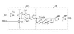
도 1은 본 발명의 제1 실시예에 따른 클럭 동기용 블럭도,
도 2는 본 발명의 제1 실시예에 따른 기동제어수단 회로도,
도 3은 본 발명의 제2 실시예에 따른 클럭 동기용 블럭도,
도 4는 본 발명의 제2 실시예에 따른 위상 합성기 회로도,
도 5는 본 발명의 제2 실시예에 따른 위상 반전 제어신호 발생기 회로도,
도 6은 본 발명의 제2 실시예에 따른 위상 반전시 위상 반전 제어신호 발생기의 타이밍도,
도 7은 본 발명의 제2 실시예에 따른 셀프 제어신호 발생기의 타이밍도,
도 8은 본 발명의 제2 실시예에 따른 클럭 동기 모드시 타이밍도, 및
도 9는 본 발명의 제2 실시예에 따른 위상 비반전시 위상 반전 제어신호 발생기의 타이밍도이다.1 is a block diagram for clock synchronization according to a first embodiment of the present invention;
2 is a circuit diagram of a start control means according to a first embodiment of the present invention;
3 is a block diagram for clock synchronization according to a second embodiment of the present invention;
4 is a phase synthesizer circuit diagram according to a second embodiment of the present invention;
5 is a circuit diagram of a phase inversion control signal generator according to a second embodiment of the present invention;
6 is a timing diagram of a phase inversion control signal generator during phase inversion according to a second embodiment of the present invention;
7 is a timing diagram of a self control signal generator according to a second embodiment of the present invention;
8 is a timing diagram in a clock synchronizing mode according to a second embodiment of the present invention, and
9 is a timing diagram of a phase inversion control signal generator during phase non-inversion according to the second embodiment of the present invention.
이하, 본 발명의 바람직한 실시예(들)에 대하여 첨부도면을 참조하여 상세히 설명한다. 우선 각 도면의 구성요소들에 참조부호를 부가함에 있어서, 동일한 구성요소들에 한해서는 비록 다른 도면상에 표시되더라도 가능한 한 동일한 부호로 표기되었음에 유의하여야 한다. 또한, 하기의 설명에서는 많은 특정사항들이 도시되어 있는데, 이는 본 발명의 보다 전반적인 이해를 돕기 위해서 제공된 것일 뿐 이러한 특정 사항들 없이도 본 발명이 실시될 수 있음은 이 기술분야에서 통상의 지식을 가진 자에게는 자명하다 할 것이다.
Hereinafter, exemplary embodiment (s) of the present invention will be described in detail with reference to the accompanying drawings. First, in adding reference numerals to the elements of each drawing, it should be noted that the same elements are denoted by the same reference numerals as much as possible even if they are displayed on different drawings. In addition, many specific details are shown in the following description, which is provided to help a more general understanding of the present invention, and the present invention may be practiced without these specific details. Will be self-evident.
도 1은 본 발명의 제1 실시예에 따른 클럭 동기용 블럭도이다.1 is a block diagram for clock synchronization according to a first embodiment of the present invention.
본 발명의 제1 실시예에 따른 클럭 동기용 블럭도는, 서로 다른 주파수를 가진 복수의 클럭의 위상을 비교하여 위상비교신호(PDout)를 출력하는 비교수단(110); 복수의 클럭의 위상이 상이하면 비교수단 내 복수의 클럭 중 어느 하나의 위상을 반전시키기 위한 위상 반전 제어신호를 생성하는 위상반전제어수단(120); 및 외부로부터 인가되는 클럭 인에이블 신호를 이용하여 비교수단을 기동시키는 기동제어신호를 생성하는 기동제어수단(130)을 포함한다.A block diagram for clock synchronization according to a first embodiment of the present invention includes: comparison means (110) for comparing phases of a plurality of clocks having different frequencies and outputting a phase comparison signal (PDout); Phase inversion control means (120) for generating a phase inversion control signal for inverting the phase of any one of the plurality of clocks in the comparison means if the phases of the plurality of clocks are different; And start control means 130 for generating a start control signal for starting the comparison means by using a clock enable signal applied from the outside.
본 발명의 일실시예에 따른 비교수단(110)은 시스템 클럭(HCK)과 데이터 클럭(WCK)을 외부의 컨트롤러로부터 입력받기 위한 클럭 입력부(111, 113), 데이터 분주클럭(iWCLK)이 시스템 클럭(HCK)과 동일한 주파수를 갖도록 데이터 클럭(WCK)의 주파수를 분주하여 데이터 분주클럭(iWCLK)을 생성하되, 위상반전신호(Reverse)에 따라 데이터 분주클럭(iWCLK)의 위상을 반전시켜 출력하기 위한 클럭분주부(115, 117), 클럭 입력부(111)로부터 출력되는 내부 시스템 클럭(iCLK)과 데이터 분주클럭(iWCLK)의 위상을 비교하여 위상비교신호(PDout)를 출력하는 비교부(119)를 포함한다.Comparing means 110 according to an embodiment of the present invention is a
클럭 입력부(111, 113)는 시스템 클럭(HCK)을 입력받아 버퍼링하여 출력하는 클럭 버퍼(111)와 데이터 클럭(WCK)을 입력받아 버퍼링하여 출력하는 클럭 버퍼(113)를 포함한다.The
클럭분주부(115, 117)는 시스템 클럭(HCK)과 동일한 주파수를 갖도록 데이터 클럭(WCK)의 주파수를 분주하는 분주기(115)와, 분주기(115)의 출력을 이용하여 위상이 서로 다른 복수의 데이터 분주클럭(iCLK)을 출력하는 다중 위상 클럭 발생기(117)를 포함한다.The
비교부(119)는 복수의 데이터 분주클럭(iWCLK) 중 어느 하나와 내부 시스템 클럭(iCLK)의 위상을 비교하여 같으면 "H"레벨신호를, 다르면 "L"레벨신호를 출력한다.The
여기서, 시스템 클럭(HCK)은 어드레스 신호 및 커맨드 신호의 입력시점을 동기시키는 데에 사용되며, 데이터 클럭(WCK)은 데이터 신호의 입력시점을 동기시키는 데에 사용된다. 그리고, 데이터 클럭(WCK)은 시스템 클럭(HCK)보다 높은 주파수를 가진다.Here, the system clock HCK is used to synchronize the input time of the address signal and the command signal, and the data clock WCK is used to synchronize the input time of the data signal. The data clock WCK has a higher frequency than the system clock HCK.
본 발명의 일실시예에 따른 위상반전제어수단(120)은 기수개의 인버터로 구현될 수 있고, 비교부(119)의 출력을 반전시킨 위상반전신호(Reverse)를 출력한다.Phase inversion control means 120 according to an embodiment of the present invention may be implemented with an odd number of inverters, and outputs a phase inversion signal (Reverse) inverted the output of the
본 발명의 일실시예에 따른 비교종료수단(140)은 내부 시스템 클럭(iCLK)에 동기하여 자신의 출력인 비교종료신호(PDEnd)에 응답하는 신호를 출력하는 플립플롭(F/F)을 포함한다.
Comparing end means 140 according to an embodiment of the present invention includes a flip-flop (F / F) for outputting a signal in response to the comparison end signal PDEnd, which is its output in synchronization with the internal system clock (iCLK) do.
도 2는 본 발명의 제1 실시예에 따른 기동제어수단(130) 회로도이다.2 is a circuit diagram of the start control means 130 according to the first embodiment of the present invention.
본 발명의 일실시예에 따른 기동제어수단(130)은 클럭 인에이블 신호(CKE)가 입력되면 제1 레벨(예컨대, "H"신호)의 위상 검출 인에이블 신호(PDenable)를 출력하고, 비교종료신호(PDEnd)가 입력되면 제2 레벨(예컨대, "L"신호)의 위상 검출 인에이블 신호(PDenable)를 출력하는 위상 검출 인에이블 신호 출력부(210)와 위상 검출 인에이블 신호(PDenable)를 이용하여 소정폭을 가진 리셋신호(Reset)로 출력하는 리셋신호출력부(220)를 포함한다.The start control means 130 according to an embodiment of the present invention outputs a phase detection enable signal PDenable of a first level (eg, an “H” signal) when the clock enable signal CKE is input, and compares the result. When the end signal PDEnd is input, the phase detection enable
본 발명의 제1 실시예에 따른 위상 검출 인에이블 신호 출력부(210)는, 클럭 인에이블 신호(CKE)를 반전시켜 클럭 인에이블 반전 신호(CKEB)를 출력하는 인버터(211), 클럭 인에이블 반전 신호(CKEB) 또는 비교종료신호(PDEnd)에 제어되어 전원전압 또는 접지전압을 출력하는 한쌍의 PMOS 및 NMOS(213, 215)를 포함하고, 소정의 제1 지연시간 후 전원전압 또는 접지전압을 위상 검출 인에이블 신호(PDenable)로 출력하는 버퍼(216, 217, 219)를 포함한다.The phase detection enable
본 발명의 제1 실시예에 따른 리셋신호출력부(220)는 위상 검출 인에이블 신호(PDenable)를 이용하여 소정폭을 가진 리셋신호(Reset)를 출력한다. 여기서, 소정폭은 인버터(221, 222, 223)의 개수에 따라 다르며, 인버터의 개수는 복수의 기수개이면 족하다.The reset
도 3은 본 발명의 제2 실시예에 따른 클럭 동기용 블럭도이고, 도 4는 본 발명의 제2 실시예에 따른 위상 검출 합성기 회로도이며, 도 5는 본 발명의 제2 실시예에 따른 위상 반전 제어신호 발생기 회로도이다.3 is a block diagram for clock synchronization according to a second embodiment of the present invention, FIG. 4 is a circuit diagram of a phase detection synthesizer according to a second embodiment of the present invention, and FIG. 5 is a phase according to a second embodiment of the present invention. Inverted control signal generator circuit diagram.
본 발명의 제2 실시예에 따른 클럭 동기용 블럭도는, 서로 다른 주파수를 가진 복수의 클럭의 위상을 비교하는 비교수단(310); 복수의 클럭의 위상이 상이하면 비교수단 내 복수의 클럭 중 어느 하나의 위상을 반전시키기 위한 위상 반전 제어신호를 생성하는 위상반전제어수단(320-1, 320-2); 외부로부터 인가되는 클럭 인에이블 신호를 이용하여 비교수단을 기동시키는 기동제어신호를 생성하는 기동제어수단(330); 및 내부 시스템 클럭(iCLK)에 동기하여 자신의 출력인 비교종료신호(PDEnd)에 응답하는 신호를 출력하는 직렬연결된 복수의 플립플롭(F/F)을 포함하는 비교종료수단(340)을 포함한다.A block diagram for clock synchronization according to a second embodiment of the present invention includes: comparing means (310) for comparing phases of a plurality of clocks having different frequencies; Phase inversion control means (320-1, 320-2) for generating a phase inversion control signal for inverting the phase of any one of the plurality of clocks in the comparison means when the phases of the plurality of clocks are different; Start control means (330) for generating a start control signal for starting the comparison means by using a clock enable signal applied from the outside; And a comparison termination means 340 including a plurality of series-connected flip-flops F / F for outputting a signal in response to the comparison termination signal PDEnd which is its output in synchronization with the internal system clock iCLK. .
본 발명의 다른 실시예에 따른 위상반전제어수단(320-1, 320-2)은 내부 시스템 클럭(iCLK)에 동기하여 비교수단(310)으로부터 출력되는 위상비교신호(PDout)에 응답하는 복수의 신호(PD1, PD2, ... , PDn)를 순차적으로 출력하는 위상 검출 유지부(320-1)와, 입력되는 복수의 신호(PD1, PD2, ... , PDn)가 모두 동일 위상이면 제1 레벨(예컨대, "H"레벨)의 위상 검출 합성 신호(PDSUMout)를 출력하는 위상 검출 합성기(Phase SUM)와, 위상 검출 합성 신호(PDSUMout)와 위상비교신호(PDout)를 이용하여 위상 반전 제어신호를 생성하는 위상 반전 제어신호 발생기(PD Reverse Gen.)를 포함한다.Phase inversion control means (320-1, 320-2) according to another embodiment of the present invention in response to the phase comparison signal (PDout) output from the comparing means 310 in synchronization with the internal system clock (iCLK) If the phase detection holding unit 320-1 for sequentially outputting the signals PD1, PD2, ..., PDn and the plurality of input signals PD1, PD2, ..., PDn are all in phase, Phase inversion control using a phase detection synthesizer (Phase SUM) for outputting a phase detection synthesis signal (PDSUMout) of one level (e.g., "H" level), and a phase detection synthesis signal (PDSUMout) and a phase comparison signal (PDout). And a phase inversion control signal generator (PD Reverse Gen.) for generating a signal.
본 발명의 다른 실시예에 따른 위상 검출 유지부(320-1)는 직렬연결된 제1 내지 제n 플립플롭(320-1, F/F1, F/F2, ... , F/Fn)을 포함하되, 제1 내지 제n 플립플롭(320-1, F/F1, F/F2, ... , F/Fn) 각각은 위상비교신호(PDout)를 내부 시스템 클럭(iCLK)에 동기하여 순차적으로 출력한다.The phase detection holding unit 320-1 according to another embodiment of the present invention includes first to n th flip-flops 320-1, F / F1, F / F2,..., F / Fn connected in series. However, each of the first to nth flip-flops 320-1, F / F1, F / F2,..., F / Fn respectively sequentially synchronizes the phase comparison signal PDout with the internal system clock iCLK. Output
본 발명의 다른 실시예에 따른 위상 검출 합성기(Phase SUM)는 위상 검출 유지부(320-1) 내 제1 내지 제n 플립플롭(320-1, F/F1, F/F2, ... , F/Fn)의 각각의 출력(PD1, PD2, ... , PDn)을 입력받아 이들 출력 모두가 동일 위상이면 제1 레벨의 위상 검출 합성 신호(PDSUMout)를 출력한다.According to another embodiment of the present invention, the phase detection synthesizer (Phase SUM) may include the first to nth flip-flops 320-1, F / F1, F / F2, ..., in the phase detection holding unit 320-1. Each of the outputs PD1, PD2, ..., PDn of F / Fn) is input and outputs a phase detection synthesis signal PDSUMout of the first level if all of these outputs are in phase.
본 발명의 다른 실시예에 따른 위상 반전 제어신호 발생기(PD Reverse Gen.)는 위상 검출 합성 신호(PDSUMout) 및 위상비교신호(PDout)의 위상이 상이하면 제1 레벨(예컨대, "H"레벨)의 위상 반전 제어신호(Reverse)를 출력하고, 위상 검출 합성 신호(PDSUMout) 및 위상비교신호(PDout)의 위상이 동일하면 제2 레벨의 위상 반전 제어신호(Reverse)를 출력한다.The phase reversal control signal generator PD Reverse Gen. according to another embodiment of the present invention has a first level (eg, an “H” level) when the phase detection synthesis signal PDSUMout and the phase comparison signal PDout are different in phase. The phase inversion control signal Reverse is outputted, and if the phase detection synthesis signal PDSUMout and the phase comparison signal PDout have the same phase, the phase inversion control signal Reverse of the second level is output.
본 발명에 따른 비교종료수단(340)은 하나 이상의 플립플롭을 포함할 수 있으며, 플립플롭의 개수는 위상반전제어수단(320) 내 플립플롭의 개수와 동일하게 구성함이 바람직하다.
The comparison termination means 340 according to the present invention may include one or more flip-flops, the number of flip-flops is preferably configured to be equal to the number of flip-flops in the phase inversion control means 320.
도 6은 본 발명의 제2 실시예에 따른 위상 반전시 위상 반전 제어신호 발생기의 타이밍도, 도 7은 본 발명의 제2 실시예에 따른 셀프 제어신호 발생기의 타이밍도, 도 8은 본 발명의 제2 실시예에 따른 클럭 동기 모드시 타이밍도, 및 도 9는 본 발명의 제2 실시예에 따른 위상 비반전시 위상 반전 제어신호 발생기의 타이밍도이다.6 is a timing diagram of a phase inversion control signal generator during phase inversion according to the second embodiment of the present invention, FIG. 7 is a timing diagram of a self control signal generator according to the second embodiment of the present invention, and FIG. 9 is a timing diagram of a clock synchronization mode according to the second embodiment, and FIG. 9 is a timing diagram of a phase inversion control signal generator during phase non-inversion according to the second embodiment of the present invention.
외부로부터 인가되는 클럭 인에이블 신호(CKE)를 이용하여 위상 검출 인에이블 신호 출력부(210)는 위상 검출 인에이블 신호(PDenable)를 생성하고, 리셋신호출력부(220)는 리셋신호(Reset)를 생성한다. 분주기(115)는 리셋신호(Reset)에 제어되어 데이터 클럭(WCK)의 주파수를 분주하여 출력하고, 비교기(119)는 위상 검출 인에이블 신호(PDenable)에 인에이블되어 데이터 분주클럭(iWCK)와 내부 시스템 클럭(iCLK)의 위상을 비교하여 출력한다.The phase detection enable
도 6을 참조하면, 비교기(119)는 두 위상이 상이하면, "L"레벨의 위상비교신호(PDout)를 출력하고, 위상 검출 유지부(320-1) 내 제1 내지 제n 플립플롭(320-1, F/F1, F/F2, ... , F/Fn) 각각은 위상비교신호(PDout)를 내부 시스템 클럭(iCLK)에 동기하여 순차적으로 출력한다.Referring to FIG. 6, when the two phases are different from each other, the
위상 검출 합성기(Phase SUM)는 위상 검출 유지부(320-1) 내 제1 내지 제n 플립플롭(320-1, F/F1, F/F2, ... , F/Fn)의 출력 모두(PD1, PD2, ..., PDn)가 동일 레벨이면 "H"레벨의 위상 검출 합성 신호(PDSUMout)를 출력한다.The phase detection synthesizer Phase SUM outputs all of the outputs of the first to nth flip-flops 320-1, F / F1, F / F2,..., F / Fn in the phase detection holding unit 320-1. If PD1, PD2, ..., PDn) are at the same level, a phase detection synthesis signal PDSUMout of "H" level is output.
도 6 및 도 9를 참조하면, 위상 반전 제어신호 발생기(PD Reverse Gen.)는 위상 검출 합성 신호(PDSUMout) 및 위상비교신호(PDout)의 위상이 상이하면 제1 레벨(예컨대, "H"레벨)의 위상 반전 제어신호(Reverse)를 출력하고, 위상 검출 합성 신호(PDSUMout) 및 위상비교신호(PDout)의 위상이 동일하면 제2 레벨의 위상 반전 제어신호(Reverse)를 출력한다.6 and 9, the phase inversion control signal generator PD Reverse Gen. has a first level (eg, an “H” level) when the phase detection synthesis signal PDSUMout and the phase comparison signal PDout are different in phase. Outputs a phase reversal control signal Reverse, and outputs a phase reversal control signal Reverse of a second level if the phase detection synthesis signal PDSUMout and the phase comparison signal PDout have the same phase.
도 7을 참조하면, 비교종료수단(340)이 비교종료신호(PDEnd)를 출력하면 위상 검출 인에이블 신호(PDenable)를 디저블시킨다.
Referring to FIG. 7, when the comparison termination means 340 outputs the comparison termination signal PDEnd, the phase termination enable signal PDen is deactivated.
한편, 본 발명에 따른 외부의 명령신호를 사용하지 않고 클럭 인에이블 신호를 이용하여 서로 다른 주파수를 가진 복수의 클럭을 동기시킬 수 있는 기술은 셀프 리프레쉬 모드, 오토 리프레쉬 모드, 액티브 파워 다운 모드, 프리차지 모드 등 저전력 상태로부터 탈출하는 경우에 활용 가능하다.
Meanwhile, a technology capable of synchronizing a plurality of clocks having different frequencies using a clock enable signal without using an external command signal according to the present invention includes a self refresh mode, an auto refresh mode, an active power down mode, and a free signal. It can be used when escaping from a low power state such as a charge mode.
또한, 본 발명은 반도체 메모리 소자의 구동뿐만 아니라 MCU(Micro Controller Unit)와 같이 서로 다른 주파수를 가진 클럭을 사용하여 고속으로 구동하는 반도체 소자에 유용하다.
In addition, the present invention is useful not only for driving semiconductor memory devices but also for semiconductor devices that are driven at high speed by using clocks having different frequencies such as MCUs (Micro Controller Units).
이와 같이, 본 발명의 상세한 설명에서는 구체적인 실시예(들)에 관해 설명하였으나, 본 발명의 범주에서 벗어나지 않는 한도 내에서 여러 가지 변형이 가능함은 물론이다. 그러므로 본 발명의 범위는 설명된 실시예(들)에 국한되어 정해져서는 안 되며, 후술하는 특허청구범위 뿐만 아니라 이 특허청구범위와 균등한 것들에 의해 정해져야 한다.
As described above, although the specific embodiment (s) have been described in the detailed description of the present invention, various modifications are possible without departing from the scope of the present invention. Therefore, the scope of the present invention should not be limited to the described embodiment (s), but should be defined by the appended claims and equivalents thereof.
110: 비교수단120: 위상반전수단
130: 기동제어수단140: 비교종료수단
310: 위상비교수단320-1, 320-2: 위상반전수단
330: 기동제어수단340: 비교종료수단110: comparison means 120: phase inversion means
130: start control means 140: comparison end means
310: phase comparison means 320-1, 320-2: phase inversion means
330: start control means 340: comparison end means
Claims (16)
Translated fromKorean상기 복수의 클럭의 위상이 상이하면 상기 비교수단 내 복수의 클럭 중 어느 하나의 위상을 반전시키기 위한 위상 반전 제어신호를 생성하는 위상반전제어수단; 및
외부로부터 인가되는 클럭 인에이블 신호를 이용하여 상기 비교수단을 기동시키는 기동제어신호를 생성하는 기동제어수단
을 포함하는 반도체 장치.
Comparison means for outputting a phase comparison signal by comparing phases of a plurality of clocks having different frequencies input from the outside;
Phase inversion control means for generating a phase inversion control signal for inverting the phase of any one of the plurality of clocks in the comparison means if the phases of the plurality of clocks are different; And
Start control means for generating a start control signal for starting the comparison means by using a clock enable signal applied from the outside
≪ / RTI >
상기 복수의 클럭의 위상이 동상이면 상기 기동제어신호의 출력을 종료하도록 제어하는 비교종료신호를 출력하는 비교종료수단을 더 포함하는 반도체 장치.
The method of claim 1,
And a comparison termination means for outputting a comparison termination signal for controlling output of the start control signal when the phases of the plurality of clocks are in phase.
외부로부터 입력되는 시스템 클럭과 데이터 클럭을 입력받기 위한 클럭 입력부;
데이터 분주클럭이 상기 시스템 클럭과 동일한 주파수를 갖도록 상기 데이터 클럭의 주파수를 분주하여 상기 데이터 분주클럭을 생성하되, 위상반전신호에 따라 상기 데이터 분주클럭의 위상을 반전시켜 출력하기 위한 클럭 분주부;
상기 클럭 입력부로부터 출력되는 내부 시스템 클럭과 상기 데이터 분주클럭의 위상을 비교하여 위상비교신호를 출력하는 비교부
를 포함하는 반도체 장치.
The method of claim 1, wherein the comparison means,
A clock input unit for receiving a system clock and a data clock input from the outside;
A clock divider for dividing a frequency of the data clock so that a data divide clock has the same frequency as the system clock to generate the data divide clock, and inverting and outputting a phase of the data divide clock according to a phase inversion signal;
A comparator for comparing a phase of an internal system clock output from the clock input part and the phase of the data division clock to output a phase comparison signal
.
상기 시스템 클럭을 입력받아 버퍼링하여 출력하는 시스템 클럭 버퍼; 및
상기 데이터 클럭을 입력받아 버퍼링하여 출력하는 데이터 클럭 버퍼
를 포함하는 반도체 장치.
The method of claim 3, wherein the clock input unit,
A system clock buffer which receives the system clock and buffers and outputs the system clock; And
A data clock buffer which receives the data clock and buffers the data clock
.
상기 시스템 클럭과 동일한 주파수를 갖도록 상기 데이터 클럭의 주파수를 분주하는 분주기; 및
상기 분주기의 출력을 이용하여 위상이 서로 다른 복수의 데이터 분주클럭을 출력하는 다중 위상 클럭 발생기
를 포함하는 반도체 장치.The clock divider of claim 3,
A divider for dividing the frequency of the data clock to have the same frequency as the system clock; And
A multi-phase clock generator for outputting a plurality of data division clocks having different phases by using the output of the divider
.
상기 위상반전제어수단은 기수개의 인버터인 것을 특징으로 하는 반도체 장치.
The method of claim 1,
And said phase inversion control means is an odd number of inverters.
상기 비교종료수단은 상기 내부 시스템 클럭에 동기하여 상기 비교종료수단의 출력인 비교종료신호에 응답하는 신호를 출력하는 플립플롭을 포함하는 것을 특징으로 하는 반도체 장치.
The method of claim 3,
And said comparing end means comprises a flip-flop for outputting a signal in response to a comparison end signal which is an output of said comparison end means in synchronization with said internal system clock.
클럭 인에이블 신호가 입력되면 제1 레벨의 위상 검출 인에이블 신호를 출력하고, 비교종료신호가 입력되면 제2 레벨의 위상 검출 인에이블 신호를 출력하는 위상 검출 인에이블 신호 출력부; 및
상기 위상 검출 인에이블 신호를 이용하여 소정폭을 가진 리셋신호로 출력하는 리셋신호출력부
를 포함하는 반도체 장치.
The method of claim 1, wherein the start control means,
A phase detection enable signal output unit configured to output a phase detection enable signal of a first level when a clock enable signal is input, and output a phase detection enable signal of a second level when a comparison end signal is input; And
Reset signal output unit for outputting a reset signal having a predetermined width by using the phase detection enable signal
.
상기 복수의 클럭의 위상이 상이하면 상기 위상비교수단 내 복수의 클럭 중 어느 하나의 위상을 반전시키기 위한 위상 반전 제어신호를 생성하는 위상반전제어수단;
외부로부터 인가되는 클럭 인에이블 신호를 이용하여 상기 위상비교수단을 기동시키는 기동제어신호를 생성하는 기동제어수단; 및
상기 위상비교수단으로부터 생성되는 내부 시스템 클럭에 동기하여 자신의 출력인 비교종료신호에 응답하는 복수의 신호를 순차적으로 출력하는 비교종료수단
을 포함하는 반도체 장치.
Phase comparison means for comparing phases of a plurality of clocks having different frequencies;
Phase inversion control means for generating a phase inversion control signal for inverting the phase of any one of the plurality of clocks in the phase comparison means if the phases of the plurality of clocks are different;
Start control means for generating a start control signal for starting the phase comparing means by using a clock enable signal applied from the outside; And
Comparison termination means for sequentially outputting a plurality of signals in response to the comparison termination signal as its output in synchronization with an internal system clock generated from the phase comparison means
≪ / RTI >
상기 내부 시스템 클럭에 동기하여 상기 위상비교수단으로부터 출력되는 위상비교신호에 응답하는 복수의 신호를 순차로 출력하는 위상 검출 유지부;
상기 위상 검출 유지부로부터 출력되는 상기 복수의 신호의 위상이 동일이면 위상 검출 합성 신호를 출력하는 위상 검출 합성기; 및
상기 위상 검출 합성 신호와 상기 위상비교신호의 위상이 상이하면 위상 반전 제어신호를 생성하는 위상 반전 제어신호 발생기
를 포함하는 반도체 장치.
The method of claim 9, wherein the phase inversion control means,
A phase detection holding unit for sequentially outputting a plurality of signals in response to the phase comparison signal output from the phase comparing unit in synchronization with the internal system clock;
A phase detection synthesizer for outputting a phase detection synthesis signal if the phases of the plurality of signals output from the phase detection holding unit are the same; And
A phase inversion control signal generator which generates a phase inversion control signal when the phase detection synthesis signal differs from the phase comparison signal;
.
상기 위상 검출 유지부는 직렬연결된 제1 내지 제n 플립플롭을 포함하되, 상기 제1 내지 제n 플립플롭 각각은 상기 위상비교신호를 상기 내부 시스템 클럭에 동기하여 순차적으로 출력하는 것을 특징으로 하는 반도체 장치.
The method of claim 10,
The phase detection holding unit includes first to nth flip-flops connected in series, wherein each of the first to nth flip-flops sequentially outputs the phase comparison signal in synchronization with the internal system clock. .
상기 비교종료수단은 하나 이상의 플립플롭을 포함하며, 상기 플립플롭의 개수는 상기 위상반전수단 내 플립플롭의 개수와 동일한 것을 특징으로 하는 반도체 장치.
10. The method of claim 9,
And the comparing end means comprises one or more flip-flops, and the number of the flip-flops is equal to the number of flip-flops in the phase shifting means.
상기 반도체 장치는, 휘발성 메모리 소자 또는 마이크로 콘트롤러 유닛인 것을 특징으로 하는 반도체 장치.
13. The method according to any one of claims 1 to 12,
And said semiconductor device is a volatile memory element or a microcontroller unit.
상기 복수의 클럭의 위상이 상이하면 상기 데이터 클럭의 위상을 반전시키기 위한 위상 반전 제어신호를 생성하는 단계; 및
외부로부터 인가되는 클럭 인에이블 신호를 이용하여 상기 위상비교신호를 출력하는 단계를 기동시키는 기동제어신호를 생성하는 단계
을 포함하는 반도체 장치의 구동방법.
Outputting a phase comparison signal by comparing phases of a plurality of clocks having different frequencies input from the outside;
Generating phase inversion control signals for inverting phases of the data clocks when phases of the plurality of clocks are different from each other; And
Generating a start control signal for starting the step of outputting the phase comparison signal using a clock enable signal applied from the outside;
Method of driving a semiconductor device comprising a.
상기 복수의 클럭의 위상이 동상이면 상기 기동제어신호의 출력을 종료하도록 제어하는 비교종료신호를 출력하는 단계
를 더 포함하는 반도체 장치의 구동방법.
15. The method of claim 14,
Outputting a comparison end signal for controlling output of the start control signal when the phases of the plurality of clocks are in phase;
Method of driving a semiconductor device further comprising.
클럭 인에이블 신호가 입력되면 제1 레벨의 위상 검출 인에이블 신호를 출력하고, 비교종료신호가 입력되면 제2 레벨의 위상 검출 인에이블 신호를 출력하는 단계; 및
상기 위상 검출 인에이블 신호를 이용하여 소정폭을 가진 리셋신호로 출력하는 단계
를 포함하는 반도체 장치의 구동방법.15. The method of claim 14, wherein generating the start control signal comprises:
Outputting a phase detection enable signal of a first level when a clock enable signal is input, and outputting a phase detection enable signal of a second level when a comparison end signal is input; And
Outputting a reset signal having a predetermined width by using the phase detection enable signal;
Method of driving a semiconductor device comprising a.
Priority Applications (2)
| Application Number | Priority Date | Filing Date | Title |
|---|---|---|---|
| KR1020110120594AKR101883652B1 (en) | 2011-11-18 | 2011-11-18 | Semiconductor device and its driving method |
| US13/411,907US8717072B2 (en) | 2011-11-18 | 2012-03-05 | Semiconductor device and method for driving the same |
Applications Claiming Priority (1)
| Application Number | Priority Date | Filing Date | Title |
|---|---|---|---|
| KR1020110120594AKR101883652B1 (en) | 2011-11-18 | 2011-11-18 | Semiconductor device and its driving method |
Publications (2)
| Publication Number | Publication Date |
|---|---|
| KR20130055078Atrue KR20130055078A (en) | 2013-05-28 |
| KR101883652B1 KR101883652B1 (en) | 2018-08-02 |
Family
ID=48426177
Family Applications (1)
| Application Number | Title | Priority Date | Filing Date |
|---|---|---|---|
| KR1020110120594AExpired - Fee RelatedKR101883652B1 (en) | 2011-11-18 | 2011-11-18 | Semiconductor device and its driving method |
Country Status (2)
| Country | Link |
|---|---|
| US (1) | US8717072B2 (en) |
| KR (1) | KR101883652B1 (en) |
Families Citing this family (6)
| Publication number | Priority date | Publication date | Assignee | Title |
|---|---|---|---|---|
| KR102272259B1 (en) | 2015-07-01 | 2021-07-06 | 삼성전자주식회사 | Semiconductor memory device having clock generation scheme based on command interworking |
| KR20190006721A (en)* | 2017-07-11 | 2019-01-21 | 에스케이하이닉스 주식회사 | Memory device |
| KR102530884B1 (en)* | 2018-04-06 | 2023-05-11 | 에스케이하이닉스 주식회사 | Semiconductor memory device and the method for operating the same |
| KR20210079121A (en) | 2019-12-19 | 2021-06-29 | 에스케이하이닉스 주식회사 | Semiconductor device and semiconductor system |
| KR20220139063A (en) | 2021-04-07 | 2022-10-14 | 에스케이하이닉스 주식회사 | Clock signal processing circuit, semiconductor apparatus and semiconductor system |
| US11901039B2 (en)* | 2021-12-20 | 2024-02-13 | Micron Technology, Inc. | Multiple differential write clock signals with different phases |
Citations (3)
| Publication number | Priority date | Publication date | Assignee | Title |
|---|---|---|---|---|
| US20070120587A1 (en)* | 2005-02-03 | 2007-05-31 | Dieter Haerle | Delay locked loop circuit and method |
| KR20100006783A (en)* | 2008-07-10 | 2010-01-21 | 주식회사 하이닉스반도체 | Semiconductor memory device |
| KR20100130335A (en)* | 2009-06-03 | 2010-12-13 | 주식회사 하이닉스반도체 | Semiconductor memory device and operation method thereof |
Family Cites Families (4)
| Publication number | Priority date | Publication date | Assignee | Title |
|---|---|---|---|---|
| WO2008074129A1 (en)* | 2006-12-21 | 2008-06-26 | Icera Canada ULC | Digital charge pump pll architecture |
| US7474136B2 (en)* | 2007-05-08 | 2009-01-06 | Promos Technologies Pte.Ltd. | Use of multiple voltage controlled delay lines for precise alignment and duty cycle control of the data output of a DDR memory device |
| US8032778B2 (en)* | 2008-03-19 | 2011-10-04 | Micron Technology, Inc. | Clock distribution apparatus, systems, and methods |
| JP5598161B2 (en)* | 2010-08-26 | 2014-10-01 | ヤマハ株式会社 | Clock generation circuit |
- 2011
- 2011-11-18KRKR1020110120594Apatent/KR101883652B1/ennot_activeExpired - Fee Related
- 2012
- 2012-03-05USUS13/411,907patent/US8717072B2/enactiveActive
Patent Citations (3)
| Publication number | Priority date | Publication date | Assignee | Title |
|---|---|---|---|---|
| US20070120587A1 (en)* | 2005-02-03 | 2007-05-31 | Dieter Haerle | Delay locked loop circuit and method |
| KR20100006783A (en)* | 2008-07-10 | 2010-01-21 | 주식회사 하이닉스반도체 | Semiconductor memory device |
| KR20100130335A (en)* | 2009-06-03 | 2010-12-13 | 주식회사 하이닉스반도체 | Semiconductor memory device and operation method thereof |
Also Published As
| Publication number | Publication date |
|---|---|
| US8717072B2 (en) | 2014-05-06 |
| KR101883652B1 (en) | 2018-08-02 |
| US20130127503A1 (en) | 2013-05-23 |
Similar Documents
| Publication | Publication Date | Title |
|---|---|---|
| US7889594B2 (en) | Semiconductor memory device | |
| US7889595B2 (en) | Semiconductor memory device | |
| US7826305B2 (en) | Latency counter, semiconductor memory device including the same, and data processing system | |
| KR100881715B1 (en) | Delayed fixed loop and its operation method | |
| KR100903370B1 (en) | Data clock training circuit, semiconductor memory device and system including same | |
| CN104699640B (en) | Semiconductor storage unit | |
| US9236101B2 (en) | Semiconductor devices including data aligner | |
| KR20130055078A (en) | Semiconductor device and its driving method | |
| KR20110024200A (en) | Semiconductor devices | |
| US9679622B2 (en) | Method for controlling memory device asynchronously with respect to system clock, and related memory device and memory system | |
| JP2011055462A (en) | Semiconductor device | |
| KR101138832B1 (en) | Semiconductor memory device and method operating the same | |
| KR20150113310A (en) | Output Controlling Circuit and Output Driving Circuit for Semiconductor Apparatus | |
| US9030907B2 (en) | Semiconductor device and semiconductor system with the same | |
| KR20140026839A (en) | Semiconductor chip and semiconductor system | |
| KR100875671B1 (en) | Semiconductor memory device comprising precharge signal generation device and driving method thereof | |
| JP2014515138A (en) | Complex data level shifter and deskew device | |
| US8254188B2 (en) | Semiconductor memory device and delay locked loop control method thereof | |
| KR20140052417A (en) | Deserializer | |
| KR100896461B1 (en) | Semiconductor device and its operation method | |
| KR101094915B1 (en) | Self-Refresh Test Circuit of Semiconductor Memory Device | |
| JP2004258888A (en) | Semiconductor integrated circuit | |
| US8179179B2 (en) | Semiconductor device | |
| KR102860712B1 (en) | Group control circuit and semiconductor memory apparatus including the same | |
| US8514005B2 (en) | Circuit and method for generating multiphase clock signals and corresponding indication signals |
Legal Events
| Date | Code | Title | Description |
|---|---|---|---|
| PA0109 | Patent application | St.27 status event code:A-0-1-A10-A12-nap-PA0109 | |
| AMND | Amendment | ||
| P11-X000 | Amendment of application requested | St.27 status event code:A-2-2-P10-P11-nap-X000 | |
| P13-X000 | Application amended | St.27 status event code:A-2-2-P10-P13-nap-X000 | |
| PN2301 | Change of applicant | St.27 status event code:A-3-3-R10-R13-asn-PN2301 St.27 status event code:A-3-3-R10-R11-asn-PN2301 | |
| PN2301 | Change of applicant | St.27 status event code:A-3-3-R10-R13-asn-PN2301 St.27 status event code:A-3-3-R10-R11-asn-PN2301 | |
| PG1501 | Laying open of application | St.27 status event code:A-1-1-Q10-Q12-nap-PG1501 | |
| PN2301 | Change of applicant | St.27 status event code:A-3-3-R10-R13-asn-PN2301 St.27 status event code:A-3-3-R10-R11-asn-PN2301 | |
| A201 | Request for examination | ||
| PA0201 | Request for examination | St.27 status event code:A-1-2-D10-D11-exm-PA0201 | |
| E902 | Notification of reason for refusal | ||
| PE0902 | Notice of grounds for rejection | St.27 status event code:A-1-2-D10-D21-exm-PE0902 | |
| AMND | Amendment | ||
| E13-X000 | Pre-grant limitation requested | St.27 status event code:A-2-3-E10-E13-lim-X000 | |
| P11-X000 | Amendment of application requested | St.27 status event code:A-2-2-P10-P11-nap-X000 | |
| P13-X000 | Application amended | St.27 status event code:A-2-2-P10-P13-nap-X000 | |
| E601 | Decision to refuse application | ||
| PE0601 | Decision on rejection of patent | St.27 status event code:N-2-6-B10-B15-exm-PE0601 | |
| AMND | Amendment | ||
| E13-X000 | Pre-grant limitation requested | St.27 status event code:A-2-3-E10-E13-lim-X000 | |
| P11-X000 | Amendment of application requested | St.27 status event code:A-2-2-P10-P11-nap-X000 | |
| P13-X000 | Application amended | St.27 status event code:A-2-2-P10-P13-nap-X000 | |
| PX0901 | Re-examination | St.27 status event code:A-2-3-E10-E12-rex-PX0901 | |
| E902 | Notification of reason for refusal | ||
| PE0902 | Notice of grounds for rejection | St.27 status event code:A-1-2-D10-D21-exm-PE0902 | |
| AMND | Amendment | ||
| P11-X000 | Amendment of application requested | St.27 status event code:A-2-2-P10-P11-nap-X000 | |
| P13-X000 | Application amended | St.27 status event code:A-2-2-P10-P13-nap-X000 | |
| PX0701 | Decision of registration after re-examination | St.27 status event code:A-3-4-F10-F13-rex-PX0701 | |
| X701 | Decision to grant (after re-examination) | ||
| E13-X000 | Pre-grant limitation requested | St.27 status event code:A-2-3-E10-E13-lim-X000 | |
| PR0701 | Registration of establishment | St.27 status event code:A-2-4-F10-F11-exm-PR0701 | |
| PR1002 | Payment of registration fee | St.27 status event code:A-2-2-U10-U11-oth-PR1002 Fee payment year number:1 | |
| PG1601 | Publication of registration | St.27 status event code:A-4-4-Q10-Q13-nap-PG1601 | |
| PR1001 | Payment of annual fee | St.27 status event code:A-4-4-U10-U11-oth-PR1001 Fee payment year number:4 | |
| PR1001 | Payment of annual fee | St.27 status event code:A-4-4-U10-U11-oth-PR1001 Fee payment year number:5 | |
| PC1903 | Unpaid annual fee | St.27 status event code:A-4-4-U10-U13-oth-PC1903 Not in force date:20230726 Payment event data comment text:Termination Category : DEFAULT_OF_REGISTRATION_FEE | |
| PC1903 | Unpaid annual fee | St.27 status event code:N-4-6-H10-H13-oth-PC1903 Ip right cessation event data comment text:Termination Category : DEFAULT_OF_REGISTRATION_FEE Not in force date:20230726 |