KR20130032199A - Organic-inorganic hybrid polymer of quantum well structure - Google Patents
Organic-inorganic hybrid polymer of quantum well structureDownload PDFInfo
- Publication number
- KR20130032199A KR20130032199AKR1020110095964AKR20110095964AKR20130032199AKR 20130032199 AKR20130032199 AKR 20130032199AKR 1020110095964 AKR1020110095964 AKR 1020110095964AKR 20110095964 AKR20110095964 AKR 20110095964AKR 20130032199 AKR20130032199 AKR 20130032199A
- Authority
- KR
- South Korea
- Prior art keywords
- tetraphenyl
- thin film
- poly
- organic
- silolsiloxane
- Prior art date
- Legal status (The legal status is an assumption and is not a legal conclusion. Google has not performed a legal analysis and makes no representation as to the accuracy of the status listed.)
- Ceased
Links
- 229920000642polymerPolymers0.000titleclaimsabstractdescription47
- 239000010409thin filmSubstances0.000claimsdescription56
- 238000003860storageMethods0.000claimsdescription24
- 238000010438heat treatmentMethods0.000claimsdescription23
- 125000001997phenyl groupChemical group[H]C1=C([H])C([H])=C(*)C([H])=C1[H]0.000claimsdescription17
- 230000004888barrier functionEffects0.000claimsdescription16
- 238000000034methodMethods0.000claimsdescription15
- KPUWHANPEXNPJT-UHFFFAOYSA-NdisiloxaneChemical class[SiH3]O[SiH3]KPUWHANPEXNPJT-UHFFFAOYSA-N0.000claimsdescription6
- 230000005684electric fieldEffects0.000claimsdescription5
- 239000010408filmSubstances0.000claimsdescription4
- 125000003118aryl groupChemical group0.000claimsdescription3
- 239000001257hydrogenSubstances0.000claimsdescription3
- 229910052739hydrogenInorganic materials0.000claimsdescription3
- 125000004435hydrogen atomChemical class[H]*0.000claimsdescription3
- 125000004450alkenylene groupChemical group0.000claimsdescription2
- 125000000217alkyl groupChemical group0.000claimsdescription2
- 125000002947alkylene groupChemical group0.000claimsdescription2
- 125000000753cycloalkyl groupChemical group0.000claimsdescription2
- 125000001072heteroaryl groupChemical group0.000claimsdescription2
- 125000001424substituent groupChemical group0.000claimsdescription2
- SRPSKMHWJZOLCR-UHFFFAOYSA-N2,3,4,5-tetraphenyl-1h-siloleChemical compound[SiH2]1C(C=2C=CC=CC=2)=C(C=2C=CC=CC=2)C(C=2C=CC=CC=2)=C1C1=CC=CC=C1SRPSKMHWJZOLCR-UHFFFAOYSA-N0.000claims1
- 239000000758substrateSubstances0.000description24
- XUIMIQQOPSSXEZ-UHFFFAOYSA-NSiliconChemical compound[Si]XUIMIQQOPSSXEZ-UHFFFAOYSA-N0.000description21
- 229910052710siliconInorganic materials0.000description20
- 239000010703siliconSubstances0.000description20
- 230000027756respiratory electron transport chainEffects0.000description13
- VLKZOEOYAKHREP-UHFFFAOYSA-Nn-HexaneChemical compoundCCCCCCVLKZOEOYAKHREP-UHFFFAOYSA-N0.000description12
- 239000002904solventSubstances0.000description12
- 229910002808Si–O–SiInorganic materials0.000description11
- 239000000463materialSubstances0.000description10
- 125000000962organic groupChemical group0.000description10
- 230000010287polarizationEffects0.000description10
- XAGFODPZIPBFFR-UHFFFAOYSA-NaluminiumChemical compound[Al]XAGFODPZIPBFFR-UHFFFAOYSA-N0.000description9
- 239000012212insulatorSubstances0.000description9
- 238000012546transferMethods0.000description9
- 230000005641tunnelingEffects0.000description9
- 238000005033Fourier transform infrared spectroscopyMethods0.000description8
- 238000004458analytical methodMethods0.000description8
- 238000002411thermogravimetryMethods0.000description8
- 230000008859changeEffects0.000description7
- 238000006116polymerization reactionMethods0.000description7
- 239000000243solutionSubstances0.000description7
- YMWUJEATGCHHMB-UHFFFAOYSA-NDichloromethaneChemical compoundClCClYMWUJEATGCHHMB-UHFFFAOYSA-N0.000description6
- 238000004833X-ray photoelectron spectroscopyMethods0.000description6
- 230000015572biosynthetic processEffects0.000description6
- 230000007423decreaseEffects0.000description6
- 238000005227gel permeation chromatographyMethods0.000description6
- 230000003993interactionEffects0.000description6
- 230000007246mechanismEffects0.000description6
- 238000000391spectroscopic ellipsometryMethods0.000description6
- 238000003775Density Functional TheoryMethods0.000description5
- 229910052782aluminiumInorganic materials0.000description5
- 239000003054catalystSubstances0.000description5
- 238000005259measurementMethods0.000description5
- 238000004776molecular orbitalMethods0.000description5
- XKRFYHLGVUSROY-UHFFFAOYSA-NArgonChemical compound[Ar]XKRFYHLGVUSROY-UHFFFAOYSA-N0.000description4
- 229910008051Si-OHInorganic materials0.000description4
- 229910006358Si—OHInorganic materials0.000description4
- QAOWNCQODCNURD-UHFFFAOYSA-NSulfuric acidChemical compoundOS(O)(=O)=OQAOWNCQODCNURD-UHFFFAOYSA-N0.000description4
- 238000010586diagramMethods0.000description4
- 125000003963dichloro groupChemical groupCl*0.000description4
- 238000004519manufacturing processMethods0.000description4
- 239000000203mixtureSubstances0.000description4
- 239000002105nanoparticleSubstances0.000description4
- 239000004065semiconductorSubstances0.000description4
- 239000007787solidSubstances0.000description4
- 238000003786synthesis reactionMethods0.000description4
- 238000005979thermal decomposition reactionMethods0.000description4
- XLYOFNOQVPJJNP-UHFFFAOYSA-NwaterChemical compoundOXLYOFNOQVPJJNP-UHFFFAOYSA-N0.000description4
- 2380000051601H NMR spectroscopyMethods0.000description3
- 238000006482condensation reactionMethods0.000description3
- 230000003247decreasing effectEffects0.000description3
- -1polydimethylsiloxanePolymers0.000description3
- 239000000843powderSubstances0.000description3
- 238000001556precipitationMethods0.000description3
- 230000008569processEffects0.000description3
- 238000010992refluxMethods0.000description3
- 239000000126substanceSubstances0.000description3
- 208000016261weight lossDiseases0.000description3
- 230000004580weight lossEffects0.000description3
- BXONXWOWYMTXSB-UHFFFAOYSA-N1-hydroxy-1H-silol-2-olChemical compoundO[SiH]1C=CC=C1OBXONXWOWYMTXSB-UHFFFAOYSA-N0.000description2
- 23800000164413C nuclear magnetic resonance spectroscopyMethods0.000description2
- KAKZBPTYRLMSJV-UHFFFAOYSA-NButadieneChemical compoundC=CC=CKAKZBPTYRLMSJV-UHFFFAOYSA-N0.000description2
- 238000005481NMR spectroscopyMethods0.000description2
- 229910018540Si CInorganic materials0.000description2
- 238000009825accumulationMethods0.000description2
- 229910052786argonInorganic materials0.000description2
- 239000012298atmosphereSubstances0.000description2
- 239000011248coating agentSubstances0.000description2
- 238000000576coating methodMethods0.000description2
- 238000009833condensationMethods0.000description2
- 230000005494condensationEffects0.000description2
- 239000003989dielectric materialSubstances0.000description2
- 238000004821distillationMethods0.000description2
- 238000001704evaporationMethods0.000description2
- 230000008020evaporationEffects0.000description2
- 230000006870functionEffects0.000description2
- 239000011261inert gasSubstances0.000description2
- 230000009878intermolecular interactionEffects0.000description2
- 150000002500ionsChemical class0.000description2
- 229910052751metalInorganic materials0.000description2
- 239000002184metalSubstances0.000description2
- TWNQGVIAIRXVLR-UHFFFAOYSA-Noxo(oxoalumanyloxy)alumaneChemical compoundO=[Al]O[Al]=OTWNQGVIAIRXVLR-UHFFFAOYSA-N0.000description2
- 238000000197pyrolysisMethods0.000description2
- 238000011160researchMethods0.000description2
- 229910010271silicon carbideInorganic materials0.000description2
- PWYVVBKROXXHEB-UHFFFAOYSA-Mtrimethyl-[3-(1-methyl-2,3,4,5-tetraphenylsilol-1-yl)propyl]azanium;iodideChemical compound[I-].C[N+](C)(C)CCC[Si]1(C)C(C=2C=CC=CC=2)=C(C=2C=CC=CC=2)C(C=2C=CC=CC=2)=C1C1=CC=CC=C1PWYVVBKROXXHEB-UHFFFAOYSA-M0.000description2
- HIXDQWDOVZUNNA-UHFFFAOYSA-N2-(3,4-dimethoxyphenyl)-5-hydroxy-7-methoxychromen-4-oneChemical compoundC=1C(OC)=CC(O)=C(C(C=2)=O)C=1OC=2C1=CC=C(OC)C(OC)=C1HIXDQWDOVZUNNA-UHFFFAOYSA-N0.000description1
- OKTJSMMVPCPJKN-UHFFFAOYSA-NCarbonChemical compound[C]OKTJSMMVPCPJKN-UHFFFAOYSA-N0.000description1
- 239000004793PolystyreneSubstances0.000description1
- 229910018557Si OInorganic materials0.000description1
- 229910004298SiO 2Inorganic materials0.000description1
- 239000002253acidSubstances0.000description1
- 239000003377acid catalystSubstances0.000description1
- 230000002776aggregationEffects0.000description1
- 238000004220aggregationMethods0.000description1
- 238000000137annealingMethods0.000description1
- 125000004429atomChemical group0.000description1
- 238000005284basis setMethods0.000description1
- 238000005452bendingMethods0.000description1
- XDLDASNSMGOEMX-UHFFFAOYSA-Nbenzene benzeneChemical compoundC1=CC=CC=C1.C1=CC=CC=C1XDLDASNSMGOEMX-UHFFFAOYSA-N0.000description1
- 150000001555benzenesChemical class0.000description1
- 230000005540biological transmissionEffects0.000description1
- 239000012267brineSubstances0.000description1
- 238000004364calculation methodMethods0.000description1
- 229910052799carbonInorganic materials0.000description1
- 125000004432carbon atomChemical groupC*0.000description1
- 239000000969carrierSubstances0.000description1
- 230000021615conjugationEffects0.000description1
- 238000010168coupling processMethods0.000description1
- 238000005859coupling reactionMethods0.000description1
- 238000002484cyclic voltammetryMethods0.000description1
- 230000007547defectEffects0.000description1
- 238000011161developmentMethods0.000description1
- 239000004205dimethyl polysiloxaneSubstances0.000description1
- 238000010494dissociation reactionMethods0.000description1
- 230000005593dissociationsEffects0.000description1
- 238000004090dissolutionMethods0.000description1
- 239000012153distilled waterSubstances0.000description1
- 230000000694effectsEffects0.000description1
- 239000003480eluentSubstances0.000description1
- 238000005516engineering processMethods0.000description1
- RTZKZFJDLAIYFH-UHFFFAOYSA-NetherSubstancesCCOCCRTZKZFJDLAIYFH-UHFFFAOYSA-N0.000description1
- BLBBMBKUUHYSMI-UHFFFAOYSA-Nfuran-2,3,4,5-tetrolChemical compoundOC=1OC(O)=C(O)C=1OBLBBMBKUUHYSMI-UHFFFAOYSA-N0.000description1
- 239000012535impuritySubstances0.000description1
- 238000009413insulationMethods0.000description1
- 238000004768lowest unoccupied molecular orbitalMethods0.000description1
- 230000006386memory functionEffects0.000description1
- 238000002156mixingMethods0.000description1
- 239000000178monomerSubstances0.000description1
- 239000012299nitrogen atmosphereSubstances0.000description1
- 230000003287optical effectEffects0.000description1
- 230000003647oxidationEffects0.000description1
- 238000007254oxidation reactionMethods0.000description1
- 238000005191phase separationMethods0.000description1
- 239000004033plasticSubstances0.000description1
- 229920003023plasticPolymers0.000description1
- 229920000435poly(dimethylsiloxane)Polymers0.000description1
- 229920001296polysiloxanePolymers0.000description1
- 229920002223polystyrenePolymers0.000description1
- 239000004810polytetrafluoroethyleneSubstances0.000description1
- 229920001343polytetrafluoroethylenePolymers0.000description1
- 238000005381potential energyMethods0.000description1
- 239000002244precipitateSubstances0.000description1
- 230000001376precipitating effectEffects0.000description1
- SCPYDCQAZCOKTP-UHFFFAOYSA-NsilanolChemical compound[SiH3]OSCPYDCQAZCOKTP-UHFFFAOYSA-N0.000description1
- LIVNPJMFVYWSIS-UHFFFAOYSA-Nsilicon monoxideInorganic materials[Si-]#[O+]LIVNPJMFVYWSIS-UHFFFAOYSA-N0.000description1
- HPALAKNZSZLMCH-UHFFFAOYSA-Msodium;chloride;hydrateChemical compoundO.[Na+].[Cl-]HPALAKNZSZLMCH-UHFFFAOYSA-M0.000description1
- 238000004611spectroscopical analysisMethods0.000description1
- 238000004528spin coatingMethods0.000description1
- 230000007847structural defectEffects0.000description1
- CZDYPVPMEAXLPK-UHFFFAOYSA-NtetramethylsilaneChemical compoundC[Si](C)(C)CCZDYPVPMEAXLPK-UHFFFAOYSA-N0.000description1
Images


Classifications
- C—CHEMISTRY; METALLURGY
- C08—ORGANIC MACROMOLECULAR COMPOUNDS; THEIR PREPARATION OR CHEMICAL WORKING-UP; COMPOSITIONS BASED THEREON
- C08G—MACROMOLECULAR COMPOUNDS OBTAINED OTHERWISE THAN BY REACTIONS ONLY INVOLVING UNSATURATED CARBON-TO-CARBON BONDS
- C08G77/00—Macromolecular compounds obtained by reactions forming a linkage containing silicon with or without sulfur, nitrogen, oxygen or carbon in the main chain of the macromolecule
- C08G77/04—Polysiloxanes
- C—CHEMISTRY; METALLURGY
- C09—DYES; PAINTS; POLISHES; NATURAL RESINS; ADHESIVES; COMPOSITIONS NOT OTHERWISE PROVIDED FOR; APPLICATIONS OF MATERIALS NOT OTHERWISE PROVIDED FOR
- C09D—COATING COMPOSITIONS, e.g. PAINTS, VARNISHES OR LACQUERS; FILLING PASTES; CHEMICAL PAINT OR INK REMOVERS; INKS; CORRECTING FLUIDS; WOODSTAINS; PASTES OR SOLIDS FOR COLOURING OR PRINTING; USE OF MATERIALS THEREFOR
- C09D183/00—Coating compositions based on macromolecular compounds obtained by reactions forming in the main chain of the macromolecule a linkage containing silicon, with or without sulfur, nitrogen, oxygen, or carbon only; Coating compositions based on derivatives of such polymers
- C09D183/04—Polysiloxanes
- H—ELECTRICITY
- H10—SEMICONDUCTOR DEVICES; ELECTRIC SOLID-STATE DEVICES NOT OTHERWISE PROVIDED FOR
- H10K—ORGANIC ELECTRIC SOLID-STATE DEVICES
- H10K85/00—Organic materials used in the body or electrodes of devices covered by this subclass
- C—CHEMISTRY; METALLURGY
- C08—ORGANIC MACROMOLECULAR COMPOUNDS; THEIR PREPARATION OR CHEMICAL WORKING-UP; COMPOSITIONS BASED THEREON
- C08G—MACROMOLECULAR COMPOUNDS OBTAINED OTHERWISE THAN BY REACTIONS ONLY INVOLVING UNSATURATED CARBON-TO-CARBON BONDS
- C08G77/00—Macromolecular compounds obtained by reactions forming a linkage containing silicon with or without sulfur, nitrogen, oxygen or carbon in the main chain of the macromolecule
- C08G77/80—Siloxanes having aromatic substituents, e.g. phenyl side groups
- Y—GENERAL TAGGING OF NEW TECHNOLOGICAL DEVELOPMENTS; GENERAL TAGGING OF CROSS-SECTIONAL TECHNOLOGIES SPANNING OVER SEVERAL SECTIONS OF THE IPC; TECHNICAL SUBJECTS COVERED BY FORMER USPC CROSS-REFERENCE ART COLLECTIONS [XRACs] AND DIGESTS
- Y02—TECHNOLOGIES OR APPLICATIONS FOR MITIGATION OR ADAPTATION AGAINST CLIMATE CHANGE
- Y02E—REDUCTION OF GREENHOUSE GAS [GHG] EMISSIONS, RELATED TO ENERGY GENERATION, TRANSMISSION OR DISTRIBUTION
- Y02E10/00—Energy generation through renewable energy sources
- Y02E10/50—Photovoltaic [PV] energy
- Y02E10/549—Organic PV cells
Landscapes
- Chemical & Material Sciences (AREA)
- Chemical Kinetics & Catalysis (AREA)
- Organic Chemistry (AREA)
- Engineering & Computer Science (AREA)
- Materials Engineering (AREA)
- Health & Medical Sciences (AREA)
- Medicinal Chemistry (AREA)
- Polymers & Plastics (AREA)
- Life Sciences & Earth Sciences (AREA)
- Wood Science & Technology (AREA)
- Silicon Polymers (AREA)
Abstract
Translated fromKoreanDescription
Translated fromKorean본 발명은 물리적 유연성을 가지며, 전자의 저장 및 이동이 가능한 신규한 유-무기 혼성 고분자에 관한 것이다.The present invention relates to a novel organic-inorganic hybrid polymer having physical flexibility and capable of storing and transporting electrons.
최근 들어 접거나 입을 수 있는 컴퓨터, 전자종이 등이 차세대 기술로 대두되면서 플라스틱 등 휘어질 수 있는 기판 위에서 동작할 수 있는 전자소자(플렉서블 전자소자)를 구현하기 위한 많은 연구가 이루어지고 있다.Recently, as computers and electronic papers that can be folded or worn are emerging as next-generation technologies, many researches have been conducted to realize electronic devices (flexible electronic devices) that can operate on flexible substrates such as plastics.
이를 구현하기 위해서는 휘어지는 기판이나 특수한 제작공정에서도 기존 소자의 기능을 나타낼 수 있는 새로운 물질의 개발이 필요하다.To achieve this, it is necessary to develop a new material that can represent the function of an existing device even in a curved substrate or a special manufacturing process.
유기-무기 혼성 고분자 (organic-inorganic hybrid polymer)는 유기와 무기 성분이 분자 수준에서 섞여 있는 고분자로서, 단순히 유기 또는 무기 성분 하나만을 사용했을 때에 비해 우수한 기계적, 열적, 광학적, 그리고 전기적 특성을 갖는다.Organic-inorganic hybrid polymers are polymers in which organic and inorganic components are mixed at the molecular level, and have superior mechanical, thermal, optical, and electrical properties compared to using only one organic or inorganic component.
폴리오르가노실록산(Polyorganosiloxane)은 유기그룹과 무기 -Si-O-Si- 성분이 Si-C 공유결합으로 연결된 대표적인 유-무기 혼성 고분자 중의 하나이다. 이러한 유-무기 혼성 고분자는 하기 반응식 1과 같이 Si-C 결합을 갖는 단분자(monomer)로부터 산 (또는 염기) 촉매 하에서 합성할 수 있다.Polyorganosiloxane is one of the representative organic-inorganic hybrid polymers in which an organic group and an inorganic -Si-O-Si-component are connected by a Si-C covalent bond. Such an organic-inorganic hybrid polymer can be synthesized under an acid (or base) catalyst from a monomer having a Si-C bond as shown in
[반응식 1] 산 촉매 하에서 합성가능한 전형적인 유-무기 혼성 고분자 중 하나인 실세스퀴옥산(silsesquioxane)

폴리오르가노실록산은 유전물질로서, 외부에서 전기장을 가했을 때 물질내부에서 전기적 분극이 발생한다. 대부분의 절연체는 전기장을 가했을 때 분극현상이 발생하므로 유전체라고 할 수 있으며, 폴리오르가노실록산과 같이 Si-O 결합을 갖고 있는 대부분의 물질은 큰 밴드갭에 의해 절연체일 뿐만 아니라 외부 전기장에 의한 분극현상에 의해 유전체라고 볼 수 있다.Polyorganosiloxane is a dielectric material, and electrical polarization occurs inside the material when an electric field is applied from the outside. Most of the insulators are dielectric because the polarization occurs when an electric field is applied. Most of the materials having Si-O bonds, such as polyorganosiloxanes, are not only insulators due to large band gaps, but also polarization by external electric fields. The phenomenon can be regarded as a dielectric.
대표적인 유-무기 혼성 고분자인 폴리오르가노실록산은 다양한 유기그룹이 무기 -Si-O-Si- 그룹과 공유결합을 이루고 있다. 폴리오르가노실록산 내의 유기그룹은 분자자유부피를 가지고 있어 유전율과 굴절률을 감소시키는 역할을 하며, 이는 도 1의 Lorenz-Lorentz식과 Clausius-Mosotti식을 통해 이해할 수 있다.Polyorganosiloxane, a representative organic-inorganic hybrid polymer, has various organic groups covalently bonded to inorganic -Si-O-Si- groups. The organic group in the polyorganosiloxane has a free molecular volume, which serves to reduce the dielectric constant and refractive index, which can be understood through the Lorenz-Lorentz and Clausius-Mosotti equations of FIG. 1.
낮은 주파수 영역에서는 Debye식에 따라 전체 분극을 배향 분극, 이온 분극, 그리고 전자 분극으로 나누어 생각할 수 있고, 4.74 ⅹ1014 Hz(633nm) 이상의 높은 주파수 영역에서는 전자 분극이 주로 기여하며, 이것은 Lorenz-Lorentz식으로 설명할 수 있다.In the low frequency region, the total polarization can be divided into orientation polarization, ion polarization, and electron polarization according to the Debye equation. In the high frequency region of 4.74 ⅹ 1014 Hz (633 nm) and above, electron polarization mainly contributes, which is Lorenz-Lorentz equation. It can be explained.
실리케이트-실세스퀴녹산(Silicate-silsesquioxane)의 높은 유전율은 Debye식을 이용해 Si-OH기에 의한 배향 분극에서 기인한다는 것과, 메틸렌-비페닐렌-브리지드 실세스퀴녹산(methylene-biphenylene-bridged silsesquioxane)물질의 높은 굴절률은 메틸렌-비페닐렌-브리지드기의 높은 전자 분극에 기인함이 알려진 바 있다. 또한 대한민국 공개특허 10-2007-0078894(특허문헌 1)에 개재된 바와 같이 최근에는 유전체의 전하 저장 특성이 메모리 소자로 응용 가능하다는 점에서 중요하게 연구되고 있다.The high permittivity of silicate-silsesquioxane is due to the orientation polarization by the Si-OH group using the Debye equation, and the methylene-biphenylene-bridged silsesquioxane It is known that the high refractive index of the material is due to the high electron polarization of the methylene-biphenylene-bridged group. In addition, as disclosed in Korean Patent Laid-Open Publication No. 10-2007-0078894 (Patent Document 1), in recent years, the charge storage characteristics of dielectrics have been importantly studied in that they can be applied as a memory device.
이에 따라 최근의 전자기기에서 필수적 소자인 메모리를 플렉서블 기판 위에 구현하기 위한 신소재 개발이 중요시되고 있다.Accordingly, the development of new materials for implementing a memory, which is an essential element in an electronic device, on a flexible substrate is important.
플렉서블 기판위에서 비활성 메모리 기능을 구현하기 위해서는 전하를 저장하고 유지할 수 있는 유-무기 혼성 재료의 발명이 필요한데, 지금까지 전 세계 연구자들은 주로 무기나노입자를 기존 고분자에 섞고, 무기 나노 입자에 전하를 저장하려는 시도를 해왔으나, 이러한 무기나노입자에 기반한 유-무기 혼성 재료는 무기 나노 입자들의 응집으로 발생하는 상 분리 문제 및 무기 나노 입자-고분자 계면의 결함 구조에 의해 전기적 안정성 부족의 문제가 있어왔다.In order to realize the inactive memory function on the flexible substrate, the invention of an organic-inorganic hybrid material capable of storing and maintaining electric charges is required. Until now, researchers around the world have mainly mixed inorganic nanoparticles with existing polymers and stored electric charges on inorganic nanoparticles. Although attempts have been made, organic-inorganic hybrid materials based on these inorganic nanoparticles have had problems of lack of electrical stability due to a phase separation problem caused by aggregation of inorganic nanoparticles and a defect structure of the inorganic nanoparticle-polymer interface.
종래기술의 문제점을 해결하기 위한 본 발명의 목적은 전하의 저장 및 이동이 가능하며, 물리적 유연성, 및 전기적 안정성을 갖는 신규한 유-무기 혼성 재료를 제공하는 것이다.It is an object of the present invention to solve the problems of the prior art to provide a novel organic-inorganic hybrid material which is capable of storing and transporting charges, and having physical flexibility and electrical stability.
본 발명자는 플렉시블 소자에 활용 가능한 메모리 물질에 대한 연구를 심화한 결과, 전자친화도가 우수하여 전자를 잡아둘 수 있는 사일롤 분자에 밴드갭이 커 절연 특성이 우수한 -Si-O-Si- 다리를 삽입시켜 전자를 가둘 수 있는 양자 우물 구조를 갖는 신규한 유-무기 혼성 고분자를 구현하는데 성공하여, 본 발명을 출원하기에 이르렀다.As a result of deepening the research on memory materials that can be used for flexible devices, the present inventors have found that -Si-O-Si- bridges have excellent insulation properties because they have a large band gap in silol molecules capable of trapping electrons due to their excellent electron affinity. It has been successful to implement a novel organic-inorganic hybrid polymer having a quantum well structure capable of confining electrons by inserting, and has filed the present invention.
나아가, 본 발명은 상기 유-무기 혼성 고분자의 전기적 특성을 제공하여, 본 발명에 따른 유-무기 혼성 고분자를 이용한 전자소자의 구현의 길을 제공한다.Furthermore, the present invention provides the electrical properties of the organic-inorganic hybrid polymer, thereby providing a way of implementing an electronic device using the organic-inorganic hybrid polymer according to the present invention.
본 발명은 양자 우물(Quantum Well)의 구조를 가지는 하기 화학식 1의 유-무기 혼성 고분자를 제공한다.The present invention provides an organic-inorganic hybrid polymer of Formula 1 having a structure of a quantum well.
[화학식 1][Formula 1]

상기 화학식 1에서 A1, A2,A3는 각각 CR2, CR3, CR4또는 N이고, R1,R2,R3,R4는 수소, 아릴, 알킬, 시클로알킬, 헤테로아릴이거나, 상기 R1, R2,R3,R4들 중 인접한 치환체와 C3~C7알킬렌 또는 C3~C7알케닐렌으로 연결되어 융합고리를 형성할 수 있고, n은 2~100 인 자연수이다.In
보다 구체적으로 본 발명은 따른 양자 우물(Quantum Well)의 구조를 가지는 하기 화학식 2의 유-무기 혼성 고분자를 제공한다.More specifically, the present invention provides an organic-inorganic hybrid polymer of Formula 2 having a structure of a quantum well according to the present invention.
[화학식 2][Formula 2]

상기 화학식 2에서 n은 2 ~ 100 인 자연수이다.In Formula 2, n is a natural number of 2 to 100.
상기 화학식 2의 실록산계 중합체는 폴리(테트라페닐)사일롤실록산으로서,The siloxane-based polymer of
본 발명에 따른 상기 폴리(테트라페닐)사일롤실록산의 중량평균분자량(Mw)은 800-50000의 범위를 갖는다.The weight average molecular weight (Mw) of the poly (tetraphenyl) silolsiloxane according to the present invention is 800-50000 Has a range of.
본 발명에 따른 폴리(테트라페닐)사일롤실록산의 전자 구조에서, 상기 폴리(테트라페닐)사일롤실록산의 (테트라페닐)사일롤분자에 의해 우물층이 형성되는 특징이 있으며, 상기 폴리(테트라페닐)사일롤실록산의 Si-O-Si 결합에 의해 장벽층이 형성되는 특징이 있다.In the electronic structure of the poly (tetraphenyl) silolsiloxane according to the present invention, a well layer is formed by the (tetraphenyl) silol molecule of the poly (tetraphenyl) silolsiloxane, and the poly (tetraphenyl) The barrier layer is formed by Si-O-Si bonding of silolsiloxane.
상술한 바와 같이, 본 발명에 따른 폴리(테트라페닐)사일롤실록산은 (테트라페닐)사일롤분자에 의한 우물층 및 밴드갭이 큰 Si-O-Si 결합 단위에 의한 장벽층이 형성됨에 따라, 전하의 저장이 가능한 우물 구조를 갖는 특징이 있다.As described above, as the poly (tetraphenyl) silolsiloxane according to the present invention forms a well layer made of (tetraphenyl) silol molecule and a barrier layer made of Si-O-Si bonding unit having a large band gap, It has a feature of having a well structure capable of storing charges.
상세하게, 본 발명에 따른 폴리(테트라페닐)사일롤실록산은 낮은 LUMO의 (테트라페닐)사일롤분자와 큰 HOMO-LUMO 갭의 Si-O-Si 결합이 번갈아가며 존재하여, 도 2와 같이 양자 우물(quantum well)의 전자 구조를 가진다.In detail, the poly (tetraphenyl) silolsiloxane according to the present invention is a low LUMO (tetraphenyl) silol molecule and an alternating Si-O-Si bond of a large HOMO-LUMO gap, as shown in Figure 2 It has an electronic structure of quantum wells.
보다 상세하게, 본 발명에 따른 폴리(테트라페닐)사일롤실록산은 상기 화학식 2와 같이 중합에 의해 (테트라페닐)사일롤분자가 Si-O-Si 결합으로 연결된 구조를 가짐에 따라, 장벽층(Si-O-Si 결합 단위)-우물층(사일롤 분자)이 교번된 구조를 가지며, 장벽층(Si-O-Si 결합 단위)-우물층((테트라페닐)사일롤분자)-장벽층(Si-O-Si 결합 단위)의 우물 구조가 형성되는 특징이 있다.In more detail, the poly (tetraphenyl) silolsiloxane according to the present invention has a structure in which (tetraphenyl) silol molecules are connected to Si-O-Si bonds by polymerization, as shown in
상기 화학식 2과 같이 단위체의 중합에 의해 장벽층(Si-O-Si 결합 단위)-우물층((테트라페닐)사일롤분자)이 교번 형성됨에 따라, 본 발명에 따른 폴리(테트라페닐)사일롤실록산은 상기 화학식 2의 단위체 개수와 동일한 n개의 양자 우물을 갖는다. As the barrier layer (Si-O-Si bonding unit) -well layer ((tetraphenyl) silol molecule) is alternately formed by polymerization of the unit as in
본 발명에 따른 폴리(테트라페닐)사일롤실록산은 외부 전기장의 인가시 상기 장벽층을 터널링하여 전하가 이동하는 특징이 있다. 이때, 상기 전하의 이동은 상기 우물층에 저장된 전하가 상기 장벽층을 터널링하여 폴리(테트라페닐)사일롤실록산의 외부(외부 도선)로 이동하는 경우, 외부에서 주입된 전하가 상기 장벽층을 터널링하여 상기 우물층으로 이동하는 경우 또는 상기 우물층에 저장된 전하가 상기 장벽층을 터널링하여 인접한 우물층으로 이동하는 경우를 포함한다.Poly (tetraphenyl) silolsiloxane according to the present invention is characterized in that the charge is transferred by tunneling the barrier layer upon application of an external electric field. In this case, when the charge stored in the well layer tunnels the barrier layer and moves to the outside of the poly (tetraphenyl) silolsiloxane, the charge injected from the outside tunnels the barrier layer. And moving to the well layer or a case in which charge stored in the well layer moves to the adjacent well layer by tunneling the barrier layer.
또한 본 발명은 상기 폴리(테트라페닐)사일롤실록산 함유 용액을 도포 및 열처리하여 수득된 박막을 제공한다.The present invention also provides a thin film obtained by applying and heat-treating the poly (tetraphenyl) silolsiloxane-containing solution.
이때 상기 용액은 상기 폴리(테트라페닐)사일롤실록산이 용해되는 것이라면 크게 제한적이지 않으나 THF(tetrahydroxyfurane), 헥산(hexane), 메틸렌클로라이드(methylenechloride) 등을 사용할 수 있다.In this case, the solution is not particularly limited as long as the poly (tetraphenyl) silolsiloxane is dissolved, but THF (tetrahydroxyfurane), hexane (hexane), methylene chloride (methylene chloride), or the like may be used.
또한 상기 폴리(테트라페닐)사일롤실록산 함유 용액은 1 ~ 20 중량% 의 폴리(테트라페닐)사일롤실록산을 함유하는 것이 바람직하다.In addition, the poly (tetraphenyl) silolsiloxane-containing solution preferably contains 1 to 20% by weight of poly (tetraphenyl) silolsiloxane.
본 발명에 따른 박막에 있어, 상기 폴리(테트라페닐)사일롤실록산 함유 용액이 도포된 도포막의 열처리 조건에 따라 열처리된 박막의 전기적 특성이 달라지는 특징이 있으며, 특정 열처리 조건에서 전하 전달 특성이 월등히 향상되는 특징이 있다.In the thin film according to the present invention, the electrical properties of the heat-treated thin film are changed according to the heat treatment conditions of the coating film coated with the poly (tetraphenyl) silolsiloxane-containing solution, and the charge transfer characteristics are significantly improved under specific heat treatment conditions. There is a characteristic to become.
상세하게, 도포막의 열처리조건에 따라 막 내 폴리(테트라페닐)사일롤실록산의 우물층과 우물층 간의 물리적 거리가 달라져 전하 전달 속도가 제어되는 특징이 있다.Specifically, according to the heat treatment conditions of the coating film, the physical distance between the well layer and the well layer of the poly (tetraphenyl) silolsiloxane in the film is characterized in that the charge transfer rate is controlled.
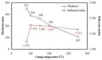
열처리는 100℃~350℃에서 수행되는 것을 특징으로 한다. 100℃이하에서는 굴절율이 급격히 떨어지고 350℃ 이상에서는 본 발명에 따른 폴리(테트라페닐)사일롤실록산의 유기그룹의 열분해로 인해 원하는 박막을 얻을 수 없다. 도 7에서 열처리 온도에 따른 굴절율과 박막두께의 변화를 나타내었다.Heat treatment is characterized in that it is carried out at 100 ℃ ~ 350 ℃. Below 100 ° C., the refractive index drops sharply and above 350 ° C., the desired thin film cannot be obtained due to thermal decomposition of the organic groups of the poly (tetraphenyl) silolsiloxane according to the invention. 7 shows the change in refractive index and thin film thickness according to the heat treatment temperature.
본 발명에 따른 박막은 굴절률이 1.55 ~ 1.62 의 범위를 가진다.The thin film according to the present invention has a refractive index in the range of 1.55 to 1.62.
본 발명에 따른 박막은 유전율이 3.0 ~ 3.5 인 특징을 가진다.The thin film according to the present invention has a feature that the dielectric constant is 3.0 to 3.5.
본 발명에 따른 박막은 △VFB(플랫밴드시프트)이 1 ~ 20 V 인 특징을 가진다.The thin film according to the present invention has a feature that ΔVFB (flat band shift) is 1 ~ 20V.
본 발명에 따른 박막은 0.03 ~ 0.06 C/㎤ 전하저장밀도를 가진다.The thin film according to the present invention has a charge storage density of 0.03 to 0.06 C /
열처리 온도는 보다 적합하게는 100℃ ~ 150℃에서 수행되는 것이 좋다.The heat treatment temperature is more preferably carried out at 100 ℃ ~ 150 ℃.
본 발명에 따른 박막에 함유되어 있는 폴리(테트라페닐)사일롤실록산의 (테트라페닐)사일롤실록산 단분자와 인접한 (테트라페닐)사일롤실록산 단분자간 두 페닐기 사이의 거리는 0.2~0.5nm 것을 특징으로 한다.The distance between the (tetraphenyl) silolsiloxane single molecule of the poly (tetraphenyl) silolsiloxane contained in the thin film according to the present invention and the adjacent (tetraphenyl) silolsiloxane single molecule is 0.2 to 0.5 nm. do.
이때, 열처리 온도가 증가할수록 페닐기 사이의 거리가 가까워져 고분자 체인간의 전자 이동 속도가 증가하고 그 결과로 양자 우물 구조에 트랩된 전자 양은 다소 감소하게 된다. 하지만 양자 우물 구조에 의한 전하 트랩 효과 자체는 사라지지 않는다.At this time, as the heat treatment temperature increases, the distance between the phenyl groups becomes closer, and thus the electron transfer speed between the polymer chains increases, and as a result, the amount of electrons trapped in the quantum well structure decreases somewhat. However, the charge trap effect by the quantum well structure does not disappear.
또한 상기 박막이 구비된 전자 소자는 본 발명의 범위에 포함된다.In addition, the electronic device provided with the thin film is included in the scope of the present invention.
상기 전자 소자로는 유기박막트랜지스터(OTFT), 비활성 메모리, 센서, 로직 회로, 메모리 회로, 튜닝 회로, 태양 전지, 연성 트랜지스터 소자, 또는 연성트랜지스터 메모리 등에서 선택될 수 있다.The electronic device may be selected from an organic thin film transistor (OTFT), an inactive memory, a sensor, a logic circuit, a memory circuit, a tuning circuit, a solar cell, a flexible transistor device, or a flexible transistor memory.
본 발명에 따른 폴리(테트라페닐)사일롤실록산은,Poly (tetraphenyl) silolsiloxane according to the present invention,
a) 디클로로(테트라페닐)사일롤을 이용하여 디하이드록시(테트라페닐)사일롤을 얻는 단계;a) obtaining dihydroxy (tetraphenyl) silol using dichloro (tetraphenyl) silol;
b) 상기 a) 단계의 디하이드록시(테트라페닐)사일롤을 환류중합하여 생성된 폴리(테트라페닐)사일롤실록산을 용해 및 침전시키는 단계;b) dissolving and precipitating the poly (tetraphenyl) silolsiloxane produced by reflux polymerization of the dihydroxy (tetraphenyl) silol of step a);
를 포함하는 제조방법으로 제조할 수 있다. 하기 반응식 2를 통하여 보다 구체적으로 나타내었다.It may be prepared by a manufacturing method comprising a. It is shown in more detail through
[반응식 2] 디하이드록시(테트라페닐)사일롤(2)과 폴리(테트라페닐)사일롤실록산(3) 합성Synthesis of dihydroxy (tetraphenyl) silol (2) and poly (tetraphenyl) silolsiloxane (3)

상기 a)단계에 대해 보다 상세하게 설명하면 다음과 같다. 디클로로(테트라페닐)사일롤(1)을 용매에 녹이고 불활성 기체분위기에서 교반한 후, 혼합물을 추출 및 세정하고, 여과 및 감압 증류하여 순수한 디하이드록시(테트라페닐)사일롤(2)을 수득할 수 있다.The above step a) will be described in more detail. After dichloro (tetraphenyl) silol (1) was dissolved in a solvent and stirred in an inert gas atmosphere, the mixture was extracted and washed, filtered and distilled under reduced pressure to obtain pure dihydroxy (tetraphenyl) silol (2). Can be.
상기 용매는 디클로로(테트라페닐)사일롤(1)을 용해하는 것이라면 제한적이지 않으나 수화 THF 등을 사용할 수 있다.The solvent is not limited as long as it dissolves dichloro (tetraphenyl) silol (1), but hydrated THF may be used.
또한 불활성 기체는 아르곤(Ar) 등을 사용할 수 있다.In addition, argon (Ar) or the like may be used as the inert gas.
상기 b)단계에 대해 보다 상세하게 설명하면 다음과 같다. 상기 디하이드록시(테트라페닐)사일롤(2)을 용매에 녹이고 환류중합반응(condensation)을 한다. 감압 증류하여 용매를 제거하고 남은 고체를 용해 및 침전(dissolution-precipitation) 과정을 거쳐 폴리(테트라페닐)사일롤실록산(3) 파우더(powder)를 수득할 수 있다.The step b) will be described in more detail below. The dihydroxy (tetraphenyl) silol (2) is dissolved in a solvent and subjected to reflux polymerization (condensation). The solvent is removed by distillation under reduced pressure, and the remaining solid is dissolved and dissolved (dissolution-precipitation) to obtain a poly (tetraphenyl) silolsiloxane (3) powder.
상기 환류중합반응은 용매 및 촉매를 넣어 수행될 수 있다.The reflux polymerization may be performed by adding a solvent and a catalyst.
이때 용매는 상기 디하이드록시(테트라페닐)사일롤(2)을 용해하는 것이라면크게 제한적이지 않으나 THF 등을 사용할 수 있다.In this case, the solvent is not particularly limited as long as it dissolves the dihydroxy (tetraphenyl) silol (2). THF may be used.
촉매 또한 크게 제한적이지 않으나 황산촉매 등을 사용하는 것이 바람직하다.The catalyst is also not particularly limited, but it is preferable to use a sulfuric acid catalyst or the like.
이때 중합은 65 ~ 67 ℃에서 2시간 이상 수행되는 것이 좋다.At this time, the polymerization is preferably carried out for at least 2 hours at 65 ~ 67 ℃.
또한 상기 용해 및 침전 과정은 감압증류하여 용매를 제거하고 남은 고체를 가용한 용매에 녹이고 헥산과 같이 비가용성 용매와 섞어 침전시키는 방법으로 제조될 수 있다.In addition, the dissolution and precipitation process may be prepared by distilling under reduced pressure to remove the solvent, dissolving the remaining solid in an available solvent, and mixing the precipitate with a non-soluble solvent such as hexane.
상술한 바와 같이, 본 발명에 따른 양자 우물 구조를 가지는 유-무기 혼성 고분자는 전하의 저장 및 이동이 가능하며, 물리적 유연성, 및 전기적인 안정성이 우수하고 제조 공정이 간편하다. 따라서 본 발명에 따른 유-무기 혼성 재료는 전하 저장 메모리 타입의 플렉서블 비휘발성 메모리로 향후 TFT 소자에 적용하여 플렉서블 비휘발성 TFT 메모리 소자를 구현할 수 있다.As described above, the organic-inorganic hybrid polymer having a quantum well structure according to the present invention is capable of storing and transporting charges, having excellent physical flexibility, electrical stability, and simple manufacturing process. Therefore, the organic-inorganic hybrid material according to the present invention is a flexible nonvolatile memory of a charge storage memory type, which can be applied to TFT devices in the future to implement a flexible nonvolatile TFT memory device.
도 1은 주파수(frequency)에 따른 분극률(polarizability)의 변화.
도 2.폴리(테트라페닐)사일롤실록산의 전하 전달을 설명하는 step potential model (SPM).
도 3. 분자오비탈에너지 다이어그램(molecular orbital energy diagram).
도 4. 폴리(테트라페닐)사일롤실록산(n=7)의 step potential model (SPM).
도 5. 폴리(테트라페닐)사일롤실록산의 TGA 결과.
도 6. 열처리 온도에 따른 폴리(테트라페닐)사일롤실록산박막의 FT-IR 결과.
도 7. SE를 통해 측정된 열처리 온도에 따른 폴리(테트라페닐)사일롤실록산박막의 굴절률과 두께 변화.
도 8. 페르미 에너지 준위(EF)를 기준으로 한 4wt% 용액으로 만든 폴리(테트라페닐)사일롤실록산박막의 분자오비탈 에너지 다이어그램(molecular orbital energy diagram).
도 9. XPS 결과를 통해 분석한 열처리 온도에 따른 폴리(테트라페닐)사일롤실록산 박막의 화학 조성의 변화.
도 10. 열처리 온도에 따른 폴리(테트라페닐)사일롤실록산박막의 C-V 커브(curve).
도 11. 양자 우물 구조의 에너지 다이어그램을 이용한 단계별 C-V 메커니즘(mechanism).
도 12. 페닐 고리의 반 데르 발스 두께를 고려한 분자 간 상호작용 모델.
도 13. △VFB와 두께(t)의 대수관계.
도 14. 반응속도론적으로 선호되는 상태(kinetially preferred state)와 열역학적으로 선호되는 상태(thermodynamically preferred state)에서의 사슬 간 거리(s)와 페닐 고리 사이의 거리(d)의 변화.
도 15. 부 바이어스 전압 정방향 스윕 조건에서의 전자 전달 속도론 모델.
도 16. 인접한 고분자 사슬의 페닐 고리 간의 co-facial 상호작용 묘사하는 기하학적 모델.1 is a change in polarizability with frequency.
Figure 2. A step potential model (SPM) illustrating the charge transfer of poly (tetraphenyl) silolsiloxane.
3. Molecular orbital energy diagram.
Figure 4. Step potential model (SPM) of poly (tetraphenyl) silolsiloxane (n = 7).
5. TGA results of poly (tetraphenyl) silolsiloxane.
6. FT-IR results of poly (tetraphenyl) silolsiloxane thin film according to heat treatment temperature.
7. Refractive index and thickness change of poly (tetraphenyl) silolsiloxane thin film according to the heat treatment temperature measured through SE.
FIG. 8. Molecular orbital energy diagram of poly (tetraphenyl) silolsiloxane thin film made from 4wt% solution based on Fermi energy level (EF).
Figure 9. Changes in chemical composition of poly (tetraphenyl) silolsiloxane thin film according to the heat treatment temperature analyzed through XPS results.
10. CV curve of poly (tetraphenyl) silolsiloxane thin film according to the heat treatment temperature.
Fig. 11. Stepwise CV mechanism using energy diagram of quantum well structure.
12. Intermolecular interaction model taking into account van der Waals thickness of the phenyl ring.
13. Algebraic relationship betweenΔV FB and thickness t.
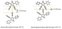
14. Change in the distance between the chains (s) and the distance (d) between the phenyl rings in the kinetially preferred state and in the thermodynamically preferred state.
15. Electron transfer kinetics model under negative bias voltage forward sweep conditions.
16. Geometric model depicting co-facial interactions between phenyl rings of adjacent polymer chains.
본 발명에서 계산된 모든 분자의 기하학적 구조는 Hyperchem 8.0 패키지(package)의 PM3 반경험적(semiempirical) 방법을 이용하여 선최적화(pre-optimization) 된 후, Gaussian03 패키지의 밀도범함수이론(density functional theory; DFT)을 이용하여 B3LYP (Becke, three-parameter, Lee-Yang-Parr) level과 6-31G** basis set에서 완전 최적화(fully optimization) 되었다.The geometric structure of all molecules calculated in the present invention is pre-optimized using the PM3 semiempirical method of the Hyperchem 8.0 package, and then the density functional theory of the Gaussian03 package; DFT) was fully optimized at B3LYP (Becke, three-parameter, Lee-Yang-Parr) level and 6-31G ** basis set.
디하이드록시(테트라페닐)사일롤과 폴리(테트라페닐)사일롤실록산의 합성Synthesis of Dihydroxy (tetraphenyl) silol and Poly (tetraphenyl) silolsiloxane
반응식 2에 합성 과정을 도식화하여 나타내었다. 디클로로(테트라페닐)사일롤(1) 2.0g (4.5 mmol)을 50mL 수화 THF (THF/H2O = 1/4)에 녹이고 아르곤(Ar) 분위기와 상온에서 2시간 동안 교반한 후, 혼합물을 에테르(ether)로 추출하고 증류수와 염수(brine) 로 씻어내고 무수 Mg2SO4를 이용해 물을 제거하여 여과하였다. 여과된 용액을 감압 증류하여 94% 수율(yield)의 밝은 녹색 고체의 순수한 디하이드록시(테트라페닐)사일롤 1.76g (4.2 mmol)을 수득하였다(: 1H-NMR (CDCl3) δ=6.8-7.2 (m, 20H), 3.0 (s, 2H)).
폴리(테트라페닐)사일롤실록산(3)은 디하이드록시(테트라페닐)사일롤(2)로부터 합성되었다. 디하이드록시(테트라페닐)사일롤(2) 1.0g (2.3 mmol)을 50mL의 THF에 녹이고 중합반응(condensation)을 위해 3.0mL의 황산(H2SO4) 촉매를 넣고 66℃를 유지하면서2시간 이상 환류(reflux)하였다. 감압 증류하여 용매를 제거하고 남은 고체를 5.0mL의 THF에 녹이고 이를 100mL의 헥산과 섞었다. 이러한 용해 및 침전(dissolution-precipitation) 과정을 3번 거친 후 60% 수율의 밝은 갈색의 폴리(테트라페닐)사일롤실록산(3) 파우더(powder) 0.6g을 수득하였다.Poly (tetraphenyl) silolsiloxane (3) was synthesized from dihydroxy (tetraphenyl) silol (2). 1.0 g (2.3 mmol) of dihydroxy (tetraphenyl) silol (2) was dissolved in 50 mL of THF, and 3.0 mL of sulfuric acid (H2 SO4 ) catalyst was added for polymerization (condensation) and maintained at 66 ° C. It was refluxed for 2 hours or more. The solvent was removed by distillation under reduced pressure, and the remaining solid was dissolved in 5.0 mL of THF and mixed with 100 mL of hexane. After three such dissolution-precipitation processes, 0.6 g of 60% yield of light brown poly (tetraphenyl) silolsiloxane (3) powder was obtained.
폴리(테트라페닐)사일롤실록산 박막 합성Poly (tetraphenyl) silolsiloxane Thin Film Synthesis
폴리(테트라페닐)사일롤실록산 0.078g을 THF 1.87g에 넣고 공기 중에서 5분간 교반하여 4wt% 폴리(테트라페닐)사일롤실록산용액을 만들고 이를 여과한 후(PTFE, 0.2 um), p-type 실리콘 기판 위에 스핀 코팅 하여(2000rpm, 25초) 폴리(테트라페닐)사일롤실록산 박막을 합성하였다. 이를 공기 중에서 80℃로 10분간 가열하여 남아 있는 용매를 제거하고, 진공 관상로(vacuum tube furnace)를 이용하여 약 1.0ⅹ10-2torr 압력하에서 1시간 동안 다음의 온도로 각각 가열하였다: 100, 150, 200, 350℃.0.078 g of poly (tetraphenyl) silolsiloxane was added to 1.87 g of THF and stirred for 5 minutes in air to form a 4 wt% poly (tetraphenyl) silolsiloxane solution, which was filtered (PTFE, 0.2 um) and then p-type silicone Spin coating on the substrate (2000 rpm, 25 seconds) to synthesize a poly (tetraphenyl) silolsiloxane thin film. It was heated in air at 80 ° C. for 10 minutes to remove the remaining solvent, and then heated to the following temperature for 1 hour under vacuum of 1.0 × 10⁻² torr using a vacuum tube furnace: 100, 150 , 200, 350 ° C.
상기 제조방법으로 제조된 폴리(테트라페닐)사일롤실록산은 다음과 같은 방법으로 분석 및 측정하였다.Poly (tetraphenyl) silolsiloxane prepared by the above production method was analyzed and measured in the following manner.
1. 겔 투과크로마토그래피(gel permeation chromatography; GPC)1. Gel permeation chromatography (GPC)
폴리(테트라페닐)사일롤실록산의 분자량은 겔 투과크로마토그래피 (GPC)를 이용하여 측정하였다 (Perkin-Elmer Series 200). Varian Polymer Laboratories columns (PLgel 5um Mixed-C and Mixed-D)를 사용하였으며, 용리액(eluent)으로 증류한 THF를 사용하였다. 분자량은 폴리스티렌 표준물질 (Varian, Easical PS-1)을 이용하여 보정하였다.The molecular weight of the poly (tetraphenyl) silolsiloxane was measured using gel permeation chromatography (GPC) (Perkin-Elmer Series 200). Varian Polymer Laboratories columns (PLgel 5um Mixed-C and Mixed-D) were used, and THF distilled with eluent was used. Molecular weights were corrected using polystyrene standards (Varian, Easical PS-1).
2. 핵자기공명분광법(nuclear magnetic spectroscopy; NMR)2. nuclear magnetic spectroscopy (NMR)
모든 NMR분석은 Bruker 300MHz 기기를 이용하였으며1H-NMR은 300.1MHz,13C-NMR은 75.5MHz를 각각 사용하였다. 테트라메틸실란(TMS)을 기준물질로 0.00ppm을 기준으로 하였으며 CDCl3를 NMR 용매로 사용하였다.All NMR analysis was performed using a Bruker 300MHz instrument1 H-NMR is 300.1MHz,13 C-NMR was used to 75.5MHz respectively. Tetramethylsilane (TMS) was based on 0.00 ppm as reference and CDCl3 was used as NMR solvent.
3. 퓨리에변환 적외선분광법 (FT-IR)3. Fourier Transform Infrared Spectroscopy (FT-IR)
폴리(테트라페닐)사일롤실록산의 분자구조는 FT-IR을 이용하여 분석하였다 (Nicolet 380). 측정범위는 4000~400 cm-1이며 분해능 7.7 cm-1, 투과율모드(transmittance mode)로 측정하였다.The molecular structure of the poly (tetraphenyl) silolsiloxane was analyzed using FT-IR (Nicolet 380). The measurement range was 4000-400 cm-1 and the resolution was measured in 7.7 cm-1 , transmission mode.
4. 열중량분석법(thermogravimetric analysis; TGA)4. thermogravimetric analysis (TGA)
TGA는 METTLER TOLEDO SDTA851e 기기를 이용하여 수행되었다. 폴리(테트라페닐)사일롤실록산파우더를 산화알루미늄(AlOx) TGA 팬에 올리고 질소 분위기(50mL/분)에서 10℃/분 속도로 30℃부터 800℃까지 가열하였다.TGA was performed using a METTLER TOLEDO SDTA851e instrument. Poly (tetraphenyl) silolsiloxane powder was placed in an aluminum oxide (AlOx) TGA pan and heated from 30 ° C. to 800 ° C. at a rate of 10 ° C./min in a nitrogen atmosphere (50 mL / min).
5. X-선 광전자분광법(X-ray photoelectron spectroscopy; XPS)5. X-ray photoelectron spectroscopy (XPS)
열처리 온도에 따른 박막의 성분 변화는 XPS를 이용하여 분석하였다. XPS 분석은 MultiLab 2000 기기를 이용하였으며 광원은 20eV pass energy 의 Mg Kα (1253.6eV)를 사용하여 1.0ⅹ10-9torr 압력 조건에서 수행하였다. 측정 전에 시료표면의 불순물을 제거하기 위해 표면을 파워 2kV, 1.3uA의 Ar+ 이온건(ion gun)으로 약 2분간 깎아내었다.The change of the composition of the thin film according to the heat treatment temperature was analyzed using XPS. XPS analysis was performed using a
6. 분광타원해석법(spectrscopic ellipsometry; SE)6. Spectroscopic ellipsometry (SE)
열처리 온도에 따른 폴리(테트라페닐)사일롤실록산박막의 두께와 굴절률은 SE를 이용하여 측정하였다 (M2000D, J.A. Wollam Co. Inc., USA).The thickness and refractive index of the poly (tetraphenyl) silolsiloxane thin film according to the heat treatment temperature were measured using SE (M2000D, J. A. Wollam Co. Inc., USA).
7. 축전용량-전압(capacitance-voltage; C-V) 측정7. Capacitance-voltage (C-V) measurement
축전용량-전압(capacitance-voltage; C-V) 측정을 위해 알루미늄 금속(aluminum metal)을 상부전극(top electrode), 폴리(테트라페닐)사일롤실록산박막을 절연체(insulator), 그리고 low-doped 실리콘 기판(silicon wafer)를 반도체(semiconductor)로 사용하여 MIS 구조를 제작하였다. 이때의 알루미늄 전극은 열적으로 (thermally) 증착되었으며, 접촉저항(contact resistance)을 줄이기 위해 실리콘 기판의 뒷면도 알루미늄 금속으로 코팅하였다.To measure capacitance-voltage (CV), aluminum metal is used as the top electrode, poly (tetraphenyl) silolsiloxane thin film as the insulator, and low-doped silicon substrate ( MIS structure was fabricated using silicon wafer as a semiconductor. At this time, the aluminum electrode was thermally deposited, and in order to reduce contact resistance, the back surface of the silicon substrate was also coated with aluminum metal.
C-V 커브(curve)는 HP4284 LCR meter를 이용하여 1MHz 주파수와 1V 진폭의 교류전압(alternating current voltage)을 가하면서 직류전압(direct current voltage) -35V ~ 35V 범위에서 측정하였다. 폴리(테트라페닐)사일롤실록산 박막의 전하 저장 기전(charge trap mechanism)을 분석하기 위해 정방향(forward direction)과 역방향(reverse direction) 모든 방향에서 C-V 커브를 측정하였다.The C-V curve was measured using a HP4284 LCR meter at a direct current voltage of -35V to 35V while applying alternating current voltage of 1MHz frequency and 1V amplitude. The C-V curves were measured in both the forward and reverse directions to analyze the charge trap mechanism of the poly (tetraphenyl) silolsiloxane thin film.
도 3은 DFT 계산된 디하이드록시 실라사이클로펜탄, 디하이드록시사일롤, 디하이드록시(테트라페닐)사일롤, (테트라페닐)사일롤 단분자 수가 2~7개인 폴리(테트라페닐)사일롤실록산, 그리고 폴리디메틸실록산의 오비탈 에너지를 비교한 것이다(2eV ~ -20eV). 각각의 HOMO(higest occupied molecular orbital)와 LUMO(lowest unoccupied molecyular orbital)는 녹색과 적색으로 표시하였다. 디하이드록시 실라사이클로펜탄과 디하이드록시사일롤의 계산 결과를 비교하면, 실라사이클로펜틸 고리에 π-결합이 첨가됨으로써 HOMO 에너지는 증가하고 LUMO에너지는 감소하였다. 사일롤(=실라사이클로펜탄)의 낮은 LUMO는 부분적으로 실리콘 원자의 σ* 오비탈과 부타디엔의 π* 오비탈의 σ*-π* 콘주게이션에 기인한 것이다.FIG. 3 is a poly (tetraphenyl) silolsiloxane having a DFT calculated dihydroxy silacyclopentane, dihydroxysilol, dihydroxy (tetraphenyl) silol, (tetraphenyl) silol monomolecule number 2-7. And orbital energy of polydimethylsiloxane (2eV ~ -20eV). Each higest occupied molecular orbital (HOMO) and lower unoccupied molecyular orbital (LUMO) is shown in green and red. Comparing the calculated results of dihydroxy silacyclopentane and dihydroxysilol, the addition of π-bond to the silacyclopentyl ring increased HOMO energy and decreased LUMO energy. The low LUMO of silol (= silacyclopentane) is due in part to the σ * -orbital of silicon atoms and the σ * -π * conjugation of π * orbital of butadiene.
도 4는 폴리(테트라페닐)사일롤실록산(n=7)의 LUMO~LUMO+6의 에너지와 모양을 이용해 간단하게 표현한 스텝 포텐셜 모델(SPM)을 나타낸 것이다. 도 4에서 보이는 바와 같이 실록산 사슬에 걸쳐 총 7개의 다른 에너지를 갖는 양자 우물(quantum well) 구조가 존재하고, 이러한 LUMO로 이루어진 양자 우물 구조가 폴리(테트라페닐)사일롤실록산분자의 (-)전하(즉, 전자) 저장의 근원일 것으로 판단된다. 도 4에 가상의 분자 간(intermolecular) 에너지 장벽은 점선으로 표시하였고 실제 이것은 도 4와 같이 일차원 형태가 아닌 삼차원 공간상에서 고분자 사슬을 감싸는 형태일 것이다. 분자 간 에너지 장벽의 길이와 높이는 두 개의 인접한 고분자 사슬 내의 테트라페닐 실롤 고리에 의존할 것이고, 전자 저장 특성을 결정하는 중요한 인자(factor) 중 하나인 고분자 사슬 간 전하 이동 속도는 분자 내 에너지 장벽보다는 분자 간 에너지 장벽에 더 큰 영향을 받을 것으로 판단된다.FIG. 4 shows a step potential model (SPM) which is simply expressed using the energy and shape of LUMO to LUMO + 6 of poly (tetraphenyl) silolsiloxane (n = 7). As shown in FIG. 4, there is a quantum well structure having a total of seven different energies across the siloxane chain, and the quantum well structure composed of this LUMO is a negative (-) charge of a poly (tetraphenyl) silolsiloxane molecule. It is believed to be the source of (ie, electronic) storage. In FIG. 4, the virtual intermolecular energy barrier is indicated by a dotted line, and in practice, this may be a form in which a polymer chain is wrapped in a three-dimensional space rather than a one-dimensional shape as shown in FIG. 4. The length and height of the intermolecular energy barrier will depend on the tetraphenyl silol ring in two adjacent polymer chains, and the rate of charge transfer between polymer chains, one of the important factors determining electron storage properties, is determined by the molecular The energy barrier is likely to be more affected.
1) 폴리(테트라페닐)사일롤실록산의 분석결과1) Analysis result of poly (tetraphenyl) silolsiloxane
- GPC 분석-GPC analysis
GPC 분석 결과, 폴리(테트라페닐)사일롤실록산의 무게평균 분자량 (weight-average molecular weight; Mw)은 약 3080, 다분산지수 (polydispersity index; Mw/Mn)는 약 1.18로 측정되었다. 단분자인 디하이드록시(테트라페닐)사일롤의 분자량이 418.6이므로 폴리(테트라페닐)사일롤실록산은 평균 약 7개의 단분자로 이루어져 있음을 알 수 있었다.As a result of GPC analysis, the weight-average molecular weight (Mw) of poly (tetraphenyl) silolsiloxane was about 3080, and the polydispersity index (Mw / Mn) was about 1.18. Since the molecular weight of the monomolecular dihydroxy (tetraphenyl) silol is 418.6, it was found that the poly (tetraphenyl) silolsiloxane consists of about 7 monomolecules on average.
- 핵자기공명(NMR) 결과-Nuclear magnetic resonance (NMR) results
1H-NMR (300.133 MHz, CDCl3): 6.45-7.19 (br, m, Ph), 1.42 (s, OH). 13C-NMR (75.403 MHz, CDCl3 (77.00)): 53.6 (s, OMe), 125-130 (m, silole 탄소), 137-137 (br, m, Ph).1 H-NMR (300.133 MHz, CDCl3 ): 6.45-7.19 (br, m, Ph), 1.42 (s, OH). 13 C-NMR (75.403 MHz, CDCl3 (77.00)): 53.6 (s, OMe), 125-130 (m, silole carbon), 137-137 (br, m, Ph).
- 열중량분석(TGA) 결과Thermogravimetric Analysis (TGA) results
본 발명의 폴리(테트라페닐)사일롤실록산은 약 90℃부터 중량감소가 일어나며 이는 물리흡착된(physisorbed) 물분자의 증발에 의한 것으로 생각된다 (도 5). 또한 약 170℃에서 2차적인 중량 감소가 일어나고 이는 고분자 말단의 실라놀(실라사이클로펜타디엔(silole)nol; Si-OH)기의 축합반응에 의해 물이 증발함으로써 발생하는 것으로 보인다. 이러한 축합반응은 다음에 언급할 폴리(테트라페닐)사일롤실록산박막의 열처리 온도에 따른 FT-IR 결과를 통해서도 예상해 볼 수 있다. 280℃ 이상에서 큰 중량 감소가 관찰되는데 이것은 유기그룹(organic group)이 열분해(thermal decomposition) 되면서 발생하는 것으로 보인다.The weight loss of the poly (tetraphenyl) silolsiloxane of the present invention occurs from about 90 ° C., which is thought to be due to the evaporation of physisorbed water molecules (FIG. 5). In addition, a secondary weight loss occurs at about 170 ° C., which appears to occur due to the evaporation of water by the condensation reaction of silanol (silolacyclopentadiene (silole) nol; Si—OH) groups at the polymer end. This condensation reaction can also be predicted through the FT-IR results according to the heat treatment temperature of the poly (tetraphenyl) silolsiloxane thin film which will be described later. A large weight loss is observed above 280 ° C., which appears to occur as the thermal decomposition of the organic groups.
2) 폴리(테트라페닐)사일롤실록산박막의 분석결과2) Analysis result of poly (tetraphenyl) silolsiloxane thin film
- FT-IR 분석 결과-FT-IR analysis result
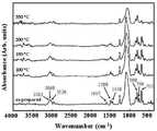
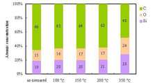
도 6은 열처리 온도에 따른 폴리(테트라페닐)사일롤실록산박막의 FT-IR 결과이다. "as-prepared" 시료의 측정 결과, 3080, 3060, 그리고 3020cm-1의 sp2-혼성화된 C-H 스트레칭과 760, 700cm-1의 단일치환된 방향족 고리 내(monosubstituted aromatic) C-H 벤딩 피크를 통해 박막 내 페닐기의 존재를 확인할 수 있었다. 온도 증가에 따라 열분해에 의한 유기그룹의 감소와 200℃ 이상에서 유기그룹이 대부분 열분해 되는 것을 볼 수 있다. 이러한 유기그룹의 열분해는 다음의 XPS 결과를 통해서도 확인할 수 있다(도 9). 1600~1400cm-1 범위의 C=C 스트레칭을 통해 박막 내 페닐기와 사일롤고리를 확인하였다. 1200~1000cm-1의 피크는 Si-O-Si의 비대칭 스트레칭(antisymmetric stretching)에 의한 것이며 800cm-1의 peak은 대칭 스트레칭(symmetric stretching)에 의한 것이다. 말단의 Si-OH기는 920cm-1 에서 측정되었으며 온도 증가에 따라 감소함을 볼 수 있다. 이는 박막 내에서 일어나는 축합반응의 간접적인 증거이다.6 is an FT-IR result of the poly (tetraphenyl) silolsiloxane thin film according to the heat treatment temperature. Measurements of “as-prepared” samples resulted in thin films through sp2 -hybridized CH stretching of 3080, 3060, and 3020 cm−1 and monosubstituted aromatic CH bending peaks of 760, 700 cm−1 . The presence of the phenyl group was confirmed. It can be seen that as the temperature increases, the organic group decreases due to pyrolysis and most of the organic group is pyrolyzed above 200 ° C. The thermal decomposition of these organic groups can also be confirmed through the following XPS results (FIG. 9). The phenyl group and the silol ring in the thin film were confirmed by stretching the C = C in the range of 1600-1400 cm-1 . The peak of 1200 ~ 1000cm-1 is due to the asymmetric stretching of Si-O-Si and the peak of 800cm-1 is due to the symmetric stretching. The terminal Si-OH group was measured at 920 cm-1 and can be seen to decrease with increasing temperature. This is indirect evidence of condensation reactions occurring in the thin film.
- SE 분석 결과-SE analysis result
도 7은 SE를 이용해 측정한 경화 온도에 따른 폴리(테트라페닐)사일록실록산 박막의 굴절률과 두께 변화를 나타낸 것이다. 100oC 이상에서는 온도 증가에 따라 굴절률이 약간 감소하는 것에 비해 80℃ 에서 100℃℃ 온도가 증가할 때는 굴절률이 급격하게 증가하는 것을 볼 수 있다. 굴절률은 박막의 밀도와 비례 관계에 있으며 이는 다음의 Lorenz-Lorentz식으로 이해할 수 있다.Figure 7 shows the refractive index and thickness change of the poly (tetraphenyl) siloxane siloxane thin film according to the curing temperature measured using SE. Above 100oC, the refractive index decreases slightly with increasing temperature, whereas the refractive index rapidly increases as the temperature increases from 80 ℃ to 100 ℃. The refractive index is proportional to the density of the thin film, which can be understood by the following Lorenz-Lorentz equation.

여기서n은 굴절률,Nj은 밀도,αj(electronic)은 electronic polarizability,
- C-V 측정결과와 전자 저장 특성 분석 결과-C-V measurement result and electronic storage characteristic analysis result
C-V 커브는 금속-절연체-반도체(metal-insulator-semiconductor; MIS) 구조에서 측정되었다. 금속은 알미늄을 열적으로 증착하였으며 반도체는 p-type 실리콘 기판을 사용하였다.C-V curves were measured in metal-insulator-semiconductor (MIS) structures. The metal thermally deposited aluminum and the semiconductor used a p-type silicon substrate.
부 바이어스 전압 하에서는 p-type 실리콘 기판의 주 전하나르개(carrier)인 정공(hole)이 절연체 층과 실리콘 기판 사이의 계면으로 모이게 되고 일반적인 C-V 커브(curve)에서 "accumulation 영역"을 나타낸다. 이때의 절연체 두께(C)는 유전율(

C는 accumulation 영역의 축전용량,A는 전극의 면적,d는 절연체의 두께, 그리고


도 10은 열처리 온도에 따른 폴리(테트라페닐)사일롤실록산박막의 C-V 측정결과이다. 모든 온도조건에서 양의(positive) △VFB(flat band shift)가 관찰되었으며 이는 음전하(전자)가 저장되었음을 의미한다. 이것은 폴리(테트라페닐)사일롤실록산이 높은 전자친화도(electron affinity)의 LUMO 에너지 준위(낮은 LUMO 에너지)를 갖기 때문이다. "as-prepared" 시료의 경우에는 평평한 커브만을 보이고 이것은 △VFB,tot(total flat band shift)가 실험적으로 가해진 전압인 35V 보다 크다는 것을 의미한다. 열처리 온도에 따른 폴리(테트라페닐)사일롤실록산 박막의 유전율은 C-V 커브에서 축전영역의 축전 용량(accumulation capacitance)과 SE측정을 이용해 얻은 두께를 이용해 계산하였다 (표 1).10 is a CV measurement result of a poly (tetraphenyl) silolsiloxane thin film according to the heat treatment temperature. Positive ΔVFB (flat band shift) was observed at all temperature conditions, indicating that negative charges (electrons) were stored. This is because poly (tetraphenyl) silolsiloxane has a high electron affinity LUMO energy level (low LUMO energy). For "as-prepared" samples, only flat curves are shown, which means thatΔV FB, tot (total flat band shift) is greater than the experimentally applied voltage of 35V. The dielectric constant of the poly (tetraphenyl) silolsiloxane thin film according to the heat treatment temperature was calculated using the capacitance obtained from the capacitance of the storage region and the SE measurement in the CV curve (Table 1).
C-V 커브의 △VFB,tot값으로부터 저장된 전하의 체적밀도(ρ; 전하 저장 밀도)를 다음의 수식을 이용하여 계산하였다. △VFB,tot는 그 원인에 따라 다음의 네 개의 항으로 나눌 수 있다:The volume density (p; charge storage density) of the stored charge was calculated from the value of ΔVFB, tot of the CV curve using the following equation.ΔV FB, tot can be divided into four terms depending on the cause:


따라서 저장된 음전하밀도(


역방향과 정방향 스윕의 전하저장밀도(


표 1. 열처리 온도에 따른 폴리(테트라페닐)사일롤실록산박막의 유전율, 플랫 밴드 시프트(flat band shift, △VFB,2), 그리고 음전하밀도.Table 1. Dielectric constant, flat band shift (ΔVFB, 2 ), and negative charge density of poly (tetraphenyl) silolsiloxane thin film according to heat treatment temperature.

표 1과 같이, 150℃ 이상의 높은 열처리온도에서는 온도가 증가함에 따라 전하저장밀도(
도 11은 C-V 커브에서 나타난 폴리(테트라페닐)사일롤실록산 박막의 전하저장 메커니즘(mechanism)을 묘사한 것이다. 150℃ 이상의 시료는 유기그룹의 열분해가 일어나기 때문에 해석에서 제외하였으며, 사슬 내 전하 이동과 관련된 에너지 장벽 대신 사슬 간 전하 이동을 표현하였다. 단순화하기 위해 에너지 준위는 HOMO, HOMO-1, LUMO, 그리고 LUMO+1 만을 표시하였다.FIG. 11 depicts the charge storage mechanism of the poly (tetraphenyl) silolsiloxane thin film shown in the C-V curve. Samples of 150 ° C or higher were excluded from the analysis because thermal decomposition of organic groups occurred, and represented the charge transfer between chains instead of the energy barrier associated with the charge transfer within the chain. For simplicity, energy levels are shown only for HOMO, HOMO-1, LUMO, and LUMO + 1.
부 바이어스(Negative bias) 전압을 가하면(②), 알미늄 금속의 전자가 터널링(tunneling) 메커니즘을 통해 고분자의 LUMO준위로 주입(injection)되고 공명 터널링(resonance-tunneling) 메커니즘을 통해 인접한 다른 고분자의 비어있는 분자 오비탈 또는 전자 진동 상태로(vibronically) 들뜬 LUMO준위로 이동한다. 이렇게 이동한 전자들은 빠르게 LUMO준위로 전자적으로(electronically) 또는 전자 진동 상태로(vibronically) 이동(de-excited) 된다. 이러한 사슬 간 전자 전달을 통해 전자는 실리콘 기판 근처의 고분자까지 전달되며 최종적으로 p-type 실리콘 기판의 전도띠(conduction band)로 이동한다. 사슬 간 전자전달속도는 동일할 것으로 예상되므로 단위 부피당 전하저장밀도는 정상상태(steady-state) 상태일 것이다. 인가한 전압이 사라지면 전자전달이 멈추게 되고 고분자 박막 내에 전자들이 갇히게 되어 C-V 커브에서 positive △VFB를 보인다 (도 11의 ③ 과 ④ 상태).When a negative bias voltage is applied (2), electrons of aluminum metal are injected into the polymer's LUMO level through the tunneling mechanism and vias of other polymers adjacent through the resonance-tunneling mechanism. Molecular orbitals or vibronically move to excited LUMO levels. The electrons thus moved are quickly de-excited electronically or vibronically to the LUMO level. Through this chain-to-chain electron transfer, electrons are transferred to the polymer near the silicon substrate and finally move to the conduction band of the p-type silicon substrate. Since the electron transfer rates between the chains are expected to be the same, the charge storage density per unit volume will be in a steady-state state. When the applied voltage disappears, electron transfer stops and electrons are trapped in the polymer thin film, which shows a positive ΔVFB in the CV curve (3 and 4 states in FIG. 11).
정 바이어스(Positive bias) 전압을 인가하는 경우에는(④), 실리콘 기판의 도핑준위 또는 원자가 전자띠(valence band)의 전자들이 터널링 메커니즘을 통해 고분자의 LUMO준위로 주입되고 부 바이어스 조건과 동일하게 반대 방향으로 전자 전달이 일어난다. 최종적으로 전자는 알미늄 금속의 페르미 준위로 이동할 것이다.In the case of applying positive bias voltage (4), electrons of doping level or valence band of the silicon substrate are injected into the polymer's LUMO level through the tunneling mechanism and are the same as the negative bias condition. Electron transfer occurs in the direction. Finally, the electrons will move to the Fermi level of the aluminum metal.
"as-prepared"와 100℃ 시료와는 달리, 150℃ 시료 결과에서 반시계 방향의 C-V 히스테리시스(hysteresis)를 볼 수 있다. 이러한 반시계 방향의 C-V 히스테리시스는 역방향 스윕(sweep) 조건(정 바이어스 조건, ④)에서의 전하 저장이 정방향 스윕 조건(부 바이어스 조건, ②)보다 많다는 것을 의미하고, 표 1의 전하저장밀도(
폴리(테트라페닐)사일롤실록산 박막에서의 전하 전달 및 저장은 다음의 간단한 속도론적 모델을 이용해 설명할 수 있다. 도 16과 같이 고분자 박막은 n개의 고분자 부피요소(volume element)의 집합으로 생각할 수 있고 면적은A, 두께는 약t/n 라고 할 수 있다 (t는 박막의 두께).


부바이어스 조건 하에서, 첫 번째 부피요소의 전하저장밀도에 대해 steady-state approximation을 적용하면: Under negative bias conditions, applying a steady-state approximation to the charge storage density of the first volume element:


폴리(테트라페닐)사일롤실록산 박막 안에서의 전자이동속도상수(


두 번째 부피요소의 경우:For the second volume element:


poly(tetraphenyl)silolesiloxane 박막 내에 모든 부피요소 사이의 전자전달속도상수가 동일하다고 가정하면,

위의 가정의 결과로, silicon 기판 바로 옆에 위치한 n번째 부피요소를 제외한 모든 부피요소에서의 전하저장밀도는 동일하다고 볼 수 있다 (


앞서 언급한대로, 폴리(테트라페닐)사일롤실록산 고분자와 실리콘 기판 사이에 Si-O-Si 결합이 존재한다면 고분자에서 실리콘기판으로의 전자전달속도상수(


전체적으로:overall:

이것을 flat band shift 관계식에 대입하면:Substituting this into a flat band shift relation:


폴리(테트라페닐)사일롤실록산 박막 내에서의 전자이동속도상수는 고분자 사슬 사이의 전자이동속도상수에 기인한다고 생각할 수 있다. 사슬 사이의 전자전달은 두 개의 인접한 (테트라페닐)사일롤 고리사이에서의 전자 터널링에 의해 일어날 것이고 이것은 공간 상에서의 전자전달로 구분지어질 수 있다. 이때의 속도상수는 거리에 따라 지수함수적으로 감소한다는 것이 잘 알려져 있다. 비례 상수를α라고 하면:The electron transfer rate constant in the poly (tetraphenyl) silolsiloxane thin film can be considered to be due to the electron transfer rate constant between the polymer chains. Electron transfer between chains will occur by electron tunneling between two adjacent (tetraphenyl) silol rings, which can be distinguished by electron transfer in space. It is well known that the velocity constant decreases exponentially with distance. If the proportional constant isα :


"C"는 인접한 실롤 고리의 페닐 고리 사이의 거리이다:"C " is the distance between the phenyl rings of adjacent silol rings:

도 16은 실리콘 기판에 수직으로 배열된n개의 고분자 집합을 가정하여 도식화 한 것이다. 여기서


부피요소(volume element)사이의 계면이 페닐고리의 상호작용에 의해 형성된다고 가정한다면,d와s사이에는 다음과 같은 기하학적 관계가 있다:Assuming that the interface between the volume elements is formed by the interaction of phenyl rings, there is a geometric relationship betweend ands :

p,q,a, 그리고
다.All.
도 12와 같이 페닐기의 반 데르 발스 두께의 반(1.70Å)을 고려한다면, s의 최소값은 약 0.85Å 으로 추정할 수 있다. 기존의 벤젠-벤젠 상호작용에 대한 논문에 따르면, 엣지-투-페이스(edge-to-face) 타입의 형태일 때는 분자 간 거리가 약 0.40Å 정도 더 짧아질 수 있는 것으로 알려져 있다 (2.50 Å 대 2.90Å). 또한 벤젠 다이머(dimer)의 경우, 분자 간 상호작용 포텐셜 에너지가 분자 간 거리가 티-쉐입드(T-shaped)와 평행 구조일 때 각각 약 3.79와 5.00Å에서 최대인 것으로 계산되었다. 따라서, 도 12의 페닐기 사이의 분자 간 거리(d)는 3.79~5.00Å 범위에 해당할 것이다. 이때의 s값은 위의 d와 s의 관계식을 이용하면 0.48~1.87Å 으로 계산된다.Considering half the thickness of van der Waals of the phenyl group (1.70 ms) as shown in Figure 12, the minimum value of s can be estimated to be about 0.85 ms. Existing papers on benzene-benzene interactions have shown that the intermolecular distance can be shorter by 0.40 μs in the form of edge-to-face type (2.50 μs). 2.90 ms). In addition, for the benzene dimer, the intermolecular interaction potential energy was calculated to be maximum at about 3.79 and 5.00 kPa when the intermolecular distance was parallel to the T-shaped structure. Therefore, the intermolecular distance (d) between the phenyl groups of FIG. At this time, the value of s is calculated as 0.48 ~ 1.87 하면 using the relationship between d and s.
"s"가 약 -0.1nm까지 감소할 수 있다고 가정하고, s의 최대값을 충분하게 0.2nm로 설정하면(-0.100 nm < s < 0.200 nm) 다음과 같은 관계식을 얻을 수 있다.Assuming that "s" can be reduced to about -0.1 nm, and the maximum value of s is sufficiently set to 0.2 nm (-0.100 nm <s <0.200 nm), the following relation can be obtained.

식 (30)을 식 (32)에 대입하면:Substituting equation (30) into equation (32):

식 (33)을 식 (28)에 대입하고 자연로그를 취하면:Substituting Eq. (33) into Eq. (28) and taking the natural log:


도 13은


비록 사슬 간 전자 터널링에 대한 붕괴상수(decay constant) β 의 이론적 계산은 아직 수행되지 않았지만, 폴리(테트라페닐)사일롤실록산박막 내에서의 전자 전달은 (테트라페닐)사일롤 내 페닐 고리 사이의 co-facial π-π 상호작용에 의해 일어난다고 예상할 수 있다. 최근 발표된 논문에 따르면, 페닐 고리 사이의 붕괴상수 β는 실험적으로 12nm-1인 것으로 결정되었다. 이 값을 이용하면, 부피요소(volume element)의 개수 n은 약 205로 추정할 수 있다. 따라서 150℃ 시료의 부피요소 전체 길이 (t/n)는 약 1.29nm 임을 알 수 있다 (표 2). 이 값은 DFT 계산을 통해 최적화된 폴리(테트라페닐)사일롤실록산유-무기 혼성 고분자(n=7)의 높이(ℓ, 약 1.39nm)와 비슷함을 알 수 있다. 식 (30) 과 식 (31)을 이용하여 80, 100, 그리고 150℃ 시료의 s와 d값도 계산하였다 (표 2).Although the theoretical calculation of the decay constant β for interchain electron tunneling has not yet been performed, the electron transfer in the poly (tetraphenyl) silolsiloxane thin film is co-linked between the phenyl rings in (tetraphenyl) silol. It can be expected to be caused by the -facial π-π interaction. According to a recently published paper, the dissociation constant β between phenyl rings was experimentally determined to be 12 nm−1 . Using this value, the number n of volume elements can be estimated as about 205. Therefore, it can be seen that the total length (t / n) of the volume element of the 150 ° C sample is about 1.29 nm (Table 2). This value is similar to the height (l, about 1.39 nm) of the optimized poly (tetraphenyl) silolsiloxane oil-inorganic hybrid polymer (n = 7) through the DFT calculation. The s and d values of 80, 100, and 150 ° C samples were also calculated using equations (30) and (31) (Table 2).
표 2. 150℃ 이하의 낮은 열처리 온도 범위에서의 사슬 간 거리(s)와 페닐 고리 사이의 거리(d)Table 2. Distance between chains (s) and distance between phenyl rings (d) at low heat treatment temperature ranges below 150 ° C

열역학적으로 선호되는 상태(thermodynamically preffered state)에서, 80℃ 시료의 s와 d값은 각각 0.322와 0.624nm로 계산되었고, 100℃ 시료의 s와 d값은 각각 0.025와 0.362nm로 감소하는 것으로 계산 결과 알 수 있다(도 14). 100℃시료의 경우, 반데르발 접촉이 일어났을 때의 거리(0.085 nm)에 비해 s값(0.025 nm)이 작은 것으로 보아 두 개의 페닐 고리의 분자 오비탈이 부분적으로 겹쳐 있음을 예상할 수 있다.In the thermodynamically preffered state, the s and d values of 80 ° C samples were calculated to be 0.322 and 0.624 nm, respectively, and the s and d values of 100 ° C samples decreased to 0.025 and 0.362 nm, respectively. It can be seen (FIG. 14). In the case of a 100 ° C sample, the s value (0.025 nm) is small compared to the distance (0.085 nm) when the van der Waal contact occurs, and it can be expected that the molecular orbitals of the two phenyl rings partially overlap.
또한, 전자 터널링의 거리에 따른 붕괴 상수(decay constant) β는 유효 에너지 장벽(△Eeff)과 다음의 관계가 있는 것으로 알려져 있다.In addition, the decay constant β according to the distance of electron tunneling is known to have the following relationship with the effective energy barrier ΔEeff .

따라서 △Eeff는 약 1.4eV로 추정되고 이는 도 4에서의 LUMO 오비탈 에너지와 vacuum 준위의 차이와 다소 비슷한 것을 알 수 있다. 이는 사슬 간 전자 터널링이 주로 인접한 페닐 고리 사이의 코-페이셜(co-facial) π-π 상호작용에 기인한 것이라는 가정과 일치함을 알 수 있다.Therefore, ΔEeff is estimated to be about 1.4 eV, which is somewhat similar to the difference between the LUMO orbital energy and the vacuum level in FIG. 4. This is consistent with the assumption that the inter-chain electron tunneling is mainly due to co-facial π-π interactions between adjacent phenyl rings.
Claims (14)
Translated fromKorean[화학식 1]

상기 화학식 1에서 A1, A2,A3는 각각 CR2, CR3, CR4또는 N이고, R1,R2,R3, R4는 수소, 아릴, 알킬, 시클로알킬, 헤테로아릴이거나, 상기 R1, R2,R3,R4들 중 인접한 치환체와 C3~C7알킬렌 또는 C3~C7알케닐렌으로 연결되어 융합고리를 형성할 수 있고, n은 2~100 인 자연수이다.An organic-inorganic hybrid polymer of Formula 1 having a quantum well structure.
[Formula 1]
In Formula 1 A1 , A2 , A3 is CR2 , CR3 , CR4 or N, and R1 , R2 , R3 , R4 is hydrogen, aryl, alkyl, cycloalkyl, heteroaryl, or R1 , R2 , R3 , It may be connected to an adjacent substituent of R4 and C3 ~ C7 alkylene or C3 ~ C7 alkenylene to form a fused ring, n is a natural number of 2 to 100.
상기 실록산계 중합체는 화학식 2의 폴리(테트라페닐사일롤)실록산인 유-무기 혼성 고분자.
[화학식 2]

(상기 화학식 2에서 n은 2 ~ 100 인 자연수이다.)The method of claim 1,
The siloxane-based polymer is a poly (tetraphenylsilol) siloxane of Formula 2 organic-inorganic hybrid polymer.
(2)
(In Formula 2, n is a natural number of 2 to 100.)
상기 폴리(테트라페닐)사일롤실록산의 중량평균분자량(Mw)은 800 ~ 50000인 유-무기 혼성 고분자.The method of claim 2,
The weight average molecular weight (Mw) of the poly (tetraphenyl) silol siloxane is 800 ~ 50000 Phosphorus-inorganic hybrid polymer.
외부 전기장의 인가시 전하는 상기 양자 우물 구조의 우물층에서 장벽층으로 터널링하여 이동하는 것을 특징으로 하는 유-무기 혼성 고분자.The method of claim 2,
The charge on application of an external electric field is an organic-inorganic hybrid polymer, characterized in that the tunnel to move from the well layer of the quantum well structure to the barrier layer.
상기 박막은 상기 유-무기 혼성 고분자 함유 용액을 도포 및 열처리하여 수득된 박막.The method of claim 5,
The thin film is a thin film obtained by applying and heat treatment of the organic-inorganic hybrid polymer-containing solution.
열처리온도는 100℃ ~ 350℃인 것을 특징으로 하는 박막.The method according to claim 6,
Thin film, characterized in that the heat treatment temperature is 100 ℃ ~ 350 ℃.
상기 박막의 굴절률은 1.55 ~ 1.62 인 것을 특징으로 하는 박막.8. The method of claim 7,
Refractive index of the thin film is characterized in that 1.55 ~ 1.62.
상기 박막의 유전율은 3.0 ~ 3.5 인 것을 특징으로 하는 박막.8. The method of claim 7,
The thin film, characterized in that the dielectric constant of 3.0 to 3.5.
상기 박막의 △VFB는 1 ~ 20 V 인 것을 특징으로 하는 박막.8. The method of claim 7,
ΔV FB of the thin film, characterized in that 1 ~ 20V.
상기 박막의 전하저장밀도는 0.03 ~ 0.06 C/㎤ 인 것을 특징으로 하는 박막.8. The method of claim 7,
The film has a charge storage density of 0.03 to 0.06 C / cm 3.
상기 박막에 함유되어 있는 폴리(테트라페닐)사일롤실록산의 (테트라페닐)사일롤실록산 단분자 간의 인접한 두 페닐기 사이의 거리는 0.2 ~ 0.5 nm 인 것을 특징으로 하는 박막.The method according to claim 6,
A thin film, characterized in that the distance between two adjacent phenyl groups between (tetraphenyl) silolsiloxane single molecules of the poly (tetraphenyl) silolsiloxane contained in the thin film is 0.2 to 0.5 nm.
상기 전자소자는 유기박막트랜지스터(OTFT), 비활성 메모리, 센서, 로직 회로, 메모리 회로, 튜닝 회로, 태양 전지, 연성 트랜지스터 소자, 또는 연성트랜지스터 메모리 로부터 선택되는 것을 특징으로 하는 전자소자.The method of claim 13,
The electronic device is selected from an organic thin film transistor (OTFT), an inactive memory, a sensor, a logic circuit, a memory circuit, a tuning circuit, a solar cell, a flexible transistor device, or a flexible transistor memory.
Priority Applications (2)
| Application Number | Priority Date | Filing Date | Title |
|---|---|---|---|
| KR1020110095964AKR20130032199A (en) | 2011-09-22 | 2011-09-22 | Organic-inorganic hybrid polymer of quantum well structure |
| US13/425,515US20130079484A1 (en) | 2011-09-22 | 2012-03-21 | Organic-inorganic hybrid polymer having quantum well structures |
Applications Claiming Priority (1)
| Application Number | Priority Date | Filing Date | Title |
|---|---|---|---|
| KR1020110095964AKR20130032199A (en) | 2011-09-22 | 2011-09-22 | Organic-inorganic hybrid polymer of quantum well structure |
Publications (1)
| Publication Number | Publication Date |
|---|---|
| KR20130032199Atrue KR20130032199A (en) | 2013-04-01 |
Family
ID=47911967
Family Applications (1)
| Application Number | Title | Priority Date | Filing Date |
|---|---|---|---|
| KR1020110095964ACeasedKR20130032199A (en) | 2011-09-22 | 2011-09-22 | Organic-inorganic hybrid polymer of quantum well structure |
Country Status (2)
| Country | Link |
|---|---|
| US (1) | US20130079484A1 (en) |
| KR (1) | KR20130032199A (en) |
Families Citing this family (4)
| Publication number | Priority date | Publication date | Assignee | Title |
|---|---|---|---|---|
| US8890234B2 (en)* | 2012-09-05 | 2014-11-18 | Kabushiki Kaisha Toshiba | Nonvolatile semiconductor memory device |
| US9189503B2 (en) | 2012-12-06 | 2015-11-17 | Microsoft Technology Licensing, Llc | Database scale-out |
| US9147615B2 (en)* | 2014-02-14 | 2015-09-29 | International Business Machines Corporation | Ambipolar synaptic devices |
| US9922818B2 (en)* | 2014-06-16 | 2018-03-20 | Versum Materials Us, Llc | Alkyl-alkoxysilacyclic compounds |
Family Cites Families (1)
| Publication number | Priority date | Publication date | Assignee | Title |
|---|---|---|---|---|
| AU2003302727A1 (en)* | 2002-10-05 | 2004-07-22 | The Regents Of The University Of California | Synthesis and use of inorganic polymer sensor for detecting nitroaromatic compounds |
- 2011
- 2011-09-22KRKR1020110095964Apatent/KR20130032199A/ennot_activeCeased
- 2012
- 2012-03-21USUS13/425,515patent/US20130079484A1/ennot_activeAbandoned
Also Published As
| Publication number | Publication date |
|---|---|
| US20130079484A1 (en) | 2013-03-28 |
Similar Documents
| Publication | Publication Date | Title |
|---|---|---|
| Cho et al. | Synthesis and characterization of thermally stable blue light-emitting polyfluorenes containing siloxane bridges | |
| Yasuda et al. | New alternative donor− acceptor arranged poly (aryleneethynylene) s and their related compounds composed of five-membered electron-accepting 1, 3, 4-thiadiazole, 1, 2, 4-triazole, or 3, 4-dinitrothiophene units: Synthesis, packing structure, and optical properties | |
| Wen et al. | Synthesis of alternating copolysiloxane with terthiophene and perylenediimide derivative pendants for involatile WORM memory device | |
| Palaniappan et al. | Block copolymer containing poly (3‐hexylthiophene) and poly (4‐vinylpyridine): Synthesis and its interaction with CdSe quantum dots for hybrid organic applications | |
| Ko et al. | Digital memory versatility of fully π-conjugated donor–acceptor hybrid polymers | |
| Zheng et al. | Charge‐storage aromatic amino compounds for nonvolatile organic transistor memory devices | |
| Kumar et al. | Properties and applications of polysilanes | |
| Alemseghed et al. | Synthesis of Di‐block Copolymers Containing Regioregular Poly (3‐hexylthiophene) and Poly (tetrahydrofuran) by a Combination of Grignard Metathesis and Cationic Polymerizations | |
| KR20130032199A (en) | Organic-inorganic hybrid polymer of quantum well structure | |
| Magaldi et al. | Hole transporting materials for perovskite solar cells: molecular versus polymeric carbazole-based derivatives | |
| Pei et al. | Ladder-like polysilsesquioxane dielectrics for organic field-effect transistor applications | |
| Choi et al. | Observation of negative charge trapping and investigation of its physicochemical origin in newly synthesized poly (tetraphenyl) silole siloxane thin films | |
| Dong et al. | Fluorene based donor‐acceptor polymer electrets for nonvolatile organic transistor memory device applications | |
| Zhang et al. | A phthalimide-and diketopyrrolopyrrole-based A 1–π–A 2 conjugated polymer for high-performance organic thin-film transistors | |
| Magurudeniya et al. | Benzodithiophene homopolymers synthesized by Grignard metathesis (GRIM) and Stille coupling polymerizations | |
| Ma et al. | The impact of benzothiadiazole on the optoelectronic performance of polymer/PC71BM blend films and their application in nir phototransistors | |
| Bhatt et al. | Synthesis, reactivity, and optoelectronic properties of poly (3‐alkenylthiophene) diblock copolymers | |
| Sun et al. | Synthesis of triphenylamine based polysiloxane as a blue phosphorescent host | |
| Nguyen et al. | Synthesis and characterization of a polyisoprene-b-polystyrene-b-poly (3-hexylthiophene) triblock copolymer | |
| Shi et al. | Synthesis, characterization, and organic field‐effect transistors study of conjugated D–A copolymers based on dialkylated naphtho [1, 2‐b: 5, 6‐b′] dithiophene/naphtho [1, 2‐b: 5, 6‐b′] difuran and benzodiathiazole/benzoxadiazole | |
| Arias et al. | Synthesis of conjugated polymers with directly coupled 2-butyloctyloxybenzodithiophene and benzothiadazole units for application as active layers in organic solar cells | |
| Imae et al. | Oligothiophenes incorporated in a polysilsesquioxane network: application to tunable transparent conductive films | |
| He et al. | [2+ 2] Cycloaddition-retroelectrocyclization reactivity and thin film transistor performances of carbazole-based platinum polyyne polymers | |
| Lee et al. | Naphthodithiophene‐Diketopyrrolopyrrole‐Based donor–Acceptor alternating π‐Conjugated polymers for Organic thin‐Film transistors | |
| Mi et al. | The synthesis and flash memory behavior of alternate copolymer containing carbazole donor and perylenediimide derivatives acceptor by the hybridization of organo-silicon |
Legal Events
| Date | Code | Title | Description |
|---|---|---|---|
| A201 | Request for examination | ||
| PA0109 | Patent application | Patent event code:PA01091R01D Comment text:Patent Application Patent event date:20110922 | |
| PA0201 | Request for examination | ||
| N231 | Notification of change of applicant | ||
| PN2301 | Change of applicant | Patent event date:20120220 Comment text:Notification of Change of Applicant Patent event code:PN23011R01D | |
| N231 | Notification of change of applicant | ||
| PN2301 | Change of applicant | Patent event date:20120403 Comment text:Notification of Change of Applicant Patent event code:PN23011R01D | |
| E902 | Notification of reason for refusal | ||
| PE0902 | Notice of grounds for rejection | Comment text:Notification of reason for refusal Patent event date:20121128 Patent event code:PE09021S01D | |
| E601 | Decision to refuse application | ||
| PE0601 | Decision on rejection of patent | Patent event date:20130329 Comment text:Decision to Refuse Application Patent event code:PE06012S01D Patent event date:20121128 Comment text:Notification of reason for refusal Patent event code:PE06011S01I | |
| PG1501 | Laying open of application |