KR20130030616A - Nonvolatile memory device - Google Patents
Nonvolatile memory deviceDownload PDFInfo
- Publication number
- KR20130030616A KR20130030616AKR1020110094211AKR20110094211AKR20130030616AKR 20130030616 AKR20130030616 AKR 20130030616AKR 1020110094211 AKR1020110094211 AKR 1020110094211AKR 20110094211 AKR20110094211 AKR 20110094211AKR 20130030616 AKR20130030616 AKR 20130030616A
- Authority
- KR
- South Korea
- Prior art keywords
- voltage
- sensing
- reference voltage
- resistance element
- variable resistance
- Prior art date
- Legal status (The legal status is an assumption and is not a legal conclusion. Google has not performed a legal analysis and makes no representation as to the accuracy of the status listed.)
- Withdrawn
Links
- 230000008859changeEffects0.000claimsdescription21
- 230000004044responseEffects0.000claimsdescription21
- 238000000034methodMethods0.000claimsdescription14
- 238000001514detection methodMethods0.000claimsdescription3
- 229910000618GeSbTeInorganic materials0.000description38
- 238000010586diagramMethods0.000description6
- 230000006870functionEffects0.000description6
- 239000012782phase change materialSubstances0.000description4
- 230000008569processEffects0.000description3
- 230000008901benefitEffects0.000description2
- 238000005086pumpingMethods0.000description2
- 230000003321amplificationEffects0.000description1
- 239000000463materialSubstances0.000description1
- 238000012986modificationMethods0.000description1
- 230000004048modificationEffects0.000description1
- 238000003199nucleic acid amplification methodMethods0.000description1
- 239000004065semiconductorSubstances0.000description1
Images


Classifications
- G—PHYSICS
- G11—INFORMATION STORAGE
- G11C—STATIC STORES
- G11C16/00—Erasable programmable read-only memories
- G11C16/02—Erasable programmable read-only memories electrically programmable
- G11C16/06—Auxiliary circuits, e.g. for writing into memory
- G—PHYSICS
- G11—INFORMATION STORAGE
- G11C—STATIC STORES
- G11C5/00—Details of stores covered by group G11C11/00
- G11C5/14—Power supply arrangements, e.g. power down, chip selection or deselection, layout of wirings or power grids, or multiple supply levels
- G11C5/147—Voltage reference generators, voltage or current regulators; Internally lowered supply levels; Compensation for voltage drops
- G—PHYSICS
- G11—INFORMATION STORAGE
- G11C—STATIC STORES
- G11C13/00—Digital stores characterised by the use of storage elements not covered by groups G11C11/00, G11C23/00, or G11C25/00
- G11C13/0002—Digital stores characterised by the use of storage elements not covered by groups G11C11/00, G11C23/00, or G11C25/00 using resistive RAM [RRAM] elements
- G11C13/0004—Digital stores characterised by the use of storage elements not covered by groups G11C11/00, G11C23/00, or G11C25/00 using resistive RAM [RRAM] elements comprising amorphous/crystalline phase transition cells
- G—PHYSICS
- G11—INFORMATION STORAGE
- G11C—STATIC STORES
- G11C13/00—Digital stores characterised by the use of storage elements not covered by groups G11C11/00, G11C23/00, or G11C25/00
- G11C13/0002—Digital stores characterised by the use of storage elements not covered by groups G11C11/00, G11C23/00, or G11C25/00 using resistive RAM [RRAM] elements
- G11C13/0021—Auxiliary circuits
- G11C13/004—Reading or sensing circuits or methods
- G—PHYSICS
- G11—INFORMATION STORAGE
- G11C—STATIC STORES
- G11C16/00—Erasable programmable read-only memories
- G11C16/02—Erasable programmable read-only memories electrically programmable
- G11C16/06—Auxiliary circuits, e.g. for writing into memory
- G11C16/26—Sensing or reading circuits; Data output circuits
- G—PHYSICS
- G11—INFORMATION STORAGE
- G11C—STATIC STORES
- G11C16/00—Erasable programmable read-only memories
- G11C16/02—Erasable programmable read-only memories electrically programmable
- G11C16/06—Auxiliary circuits, e.g. for writing into memory
- G11C16/30—Power supply circuits
- G—PHYSICS
- G11—INFORMATION STORAGE
- G11C—STATIC STORES
- G11C13/00—Digital stores characterised by the use of storage elements not covered by groups G11C11/00, G11C23/00, or G11C25/00
- G11C13/0002—Digital stores characterised by the use of storage elements not covered by groups G11C11/00, G11C23/00, or G11C25/00 using resistive RAM [RRAM] elements
- G11C13/0021—Auxiliary circuits
- G11C13/004—Reading or sensing circuits or methods
- G11C2013/0054—Read is performed on a reference element, e.g. cell, and the reference sensed value is used to compare the sensed value of the selected cell
Landscapes
- Engineering & Computer Science (AREA)
- Power Engineering (AREA)
- Chemical & Material Sciences (AREA)
- Crystallography & Structural Chemistry (AREA)
- Semiconductor Memories (AREA)
- Mram Or Spin Memory Techniques (AREA)
- Hall/Mr Elements (AREA)
Abstract
Translated fromKoreanDescription
Translated fromKorean본 발명은 반도체 설계 기술에 관한 것으로, 더욱 상세하게는 비휘발성 메모리 장치에 관한 것이다.
The present invention relates to semiconductor design techniques, and more particularly to non-volatile memory devices.
일반적으로, 비휘발성 메모리 장치는 전원이 공급되지 않아도 저장된 데이터를 보존할 수 있는 메모리 장치로서 플래시 메모리 장치(Flash memory), 상 변화 메모리 장치(PCRAM : Phase Change RAM) 등이 있다. 특히, 상 변화 메모리 장치(PCRAM)는 상 변화 물질, 대표적인 예로서 GST(게르마늄 안티몬 텔루륨)을 이용하여 메모리 셀을 구성하고, GST에 열을 가하여 정질(Crystal) 또는 비정질(Amorphous) 상태로 만듦으로써 메모리 셀에 데이터를 저장할 수 있도록 한 메모리 장치이다. 이와 같은 상 변화 메모리 장치(PCRAM)는 휘발성 메모리 장치(RAM : Random Access Memory)에 상응하는 데이터 처리 속도를 가진다.2. Description of the Related Art Generally, a nonvolatile memory device is a memory device capable of preserving stored data even when power is not supplied, such as a flash memory device, a phase change memory device (PCRAM: Phase Change RAM), and the like. Particularly, a phase-change memory device (PCRAM) constitutes a memory cell by using a phase-change material, for example, GST (germanium antimony tellurium), and applies heat to the GST to make it into a crystalline or amorphous state So that data can be stored in the memory cell. Such a phase change memory device (PCRAM) has a data processing speed corresponding to a volatile memory device (RAM: Random Access Memory).
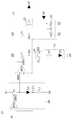
도 1에는 종래기술에 따른 상 변화 메모리 장치의 구성도가 도시되어 있다.FIG. 1 shows a block diagram of a phase change memory device according to the prior art.
도 1을 참조하면, 상 변화 메모리 장치(10)는 펌핑전압(VPPSA) 도메인을 사용하고 있으며 커런트 미러(current mirror)를 위한 신호들(BIAS, CLMBL, VCLAMP)의 제어에 따라 메모리 셀(GST, D) 경로로 센싱 커런트(sensing current)를 전달하는 방법을 사용하고 있다. 여기서, 센싱 노드(VSAI)에는 도면에 미도시되어 있지만 전압 래치(voltage latch)가 접속되며, 그 전압 래치는 상 변화 물질(GST)의 저항값에 따라 가변되는 센싱 노드(VSAI)의 전압 레벨의 차이를 센싱하게 된다. 센싱 방법을 다시 설명하면, 센싱 노드(VSAI)가 펌핑전압(VPPSA)으로 프리차지(pre-charge)된 후, 클램핑을 위한 트랜지스터(NN)의 전압 조건(Vgs, Vds)에 따라 센싱 노드(VSAI)가 디스차지(discharge)될 때 바이어스를 위한 트래지스터(P)에 흐르는 전류와 클램핑을 위한 트랜지스터(NN)에 흐르는 전류가 같아지는 때의 센싱 노드(VSAI)의 전압 레벨을 센싱하는 것이다.1, the phase-
그러나, 종래기술에 따른 상 변화 메모리 장치(10)는 센싱 노드(VSAI)가 디스차지(discharge)될 때 메모리 셀(GST, D) 경로에 존재하는 RC 시정수(time constant)의 영향 때문에, 상 변화 물질(GST)이 높은 저항값을 가질수록 센싱 노드(VSAI)가 안정화되는데 오랜 시간이 소요되는 문제점이 있다.
However, the phase
본 발명은 센싱 속도가 향상된 비휘발성 메모리 장치를 제공하는데 그 목적이 있다.It is an object of the present invention to provide a nonvolatile memory device having an improved sensing speed.
또한, 본 발명의 다른 목적은 메모리 셀에 포함된 스위칭소자에 발생하는 스큐를 보상하도록 한 비휘발성 메모리 장치를 제공하는데 그 목적이 있다.Another object of the present invention is to provide a nonvolatile memory device which compensates for skew occurring in a switching element included in a memory cell.
본 발명의 일 측면에 따르면, 본 발명은 가변저항소자와, 가변저항소자에 흐르는 전류를 제어하기 위한 스위칭소자를 포함하는 메모리 셀; 스위칭소자에 발생하는 스큐에 따라 기준전압을 가변적으로 생성하기 위한 기준전압 생성부; 및 기준전압에 기초하여 가변저항소자에 흐르는 전류에 대응하는 전압을 감지하기 위한 감지 증폭부를 포함한다.According to an aspect of the invention, the present invention provides a memory cell including a variable resistance element and a switching element for controlling a current flowing through the variable resistance element; A reference voltage generator configured to variably generate a reference voltage according to skew occurring in the switching device; And a sensing amplifier configured to sense a voltage corresponding to a current flowing through the variable resistance element based on the reference voltage.
본 발명의 다른 측면에 따르면, 본 발명은 제1 기준전압과 제1 감지전압을 비교하기 위한 제1 비교부; 제1 비교부로부터 출력되는 제1 비교신호에 응답하여 제1 감지전압단을 제1 전원전압으로 구동하기 위한 제1 구동부; 제1 감지전압단과 제2 전원전압단 사이에 접속되며, 가변저항소자와 제1 스위칭소자가 직렬로 연결된 메모리 셀; 제1 기준전압단과 분배전압단 사이에 접속되며, 제1 스위칭소자와 동일하게 설계된 제2 스위칭소자; 분배전압단과 제2 전원전압단 사이에 접속되는 고정저항소자; 제2 기준전압과 분배전압을 비교하기 위한 제2 비교부; 및 제2 비교부로부터 출력되는 제2 비교신호에 응답하여 제1 기준전압단을 제1 전원전압으로 구동하기 위한 제2 구동부를 포함한다.
According to another aspect of the invention, the present invention includes a first comparison unit for comparing the first reference voltage and the first sense voltage; A first driver for driving the first sensing voltage terminal to the first power voltage in response to the first comparison signal output from the first comparator; A memory cell connected between the first sensing voltage terminal and the second power supply voltage terminal and connected with the variable resistance element and the first switching element in series; A second switching element connected between the first reference voltage terminal and the distribution voltage terminal and designed in the same manner as the first switching element; A fixed resistance element connected between the distribution voltage terminal and the second power supply voltage terminal; A second comparator for comparing a second reference voltage and a divided voltage; And a second driver for driving the first reference voltage terminal to the first power voltage in response to the second comparison signal output from the second comparison unit.
레귤레이터 방식을 적용하여 센싱 속도가 향상되는 효과가 있다.By applying a regulator method, the sensing speed is improved.
또한, 메모리 셀에 포함된 스위칭소자에 발생하는 스큐에 대응하여 감지 증폭부에 입력되는 기준전압을 가변시킴으로써, 스위칭소자에 스큐가 발생하더라도 메모리 셀 경로에 흐르는 전류를 일정하게 유지할 수 있다. 따라서, 스위칭소자에 발생하는 스큐에 따라 메모리 셀 경로에 흐르는 전류의 변화를 감지 증폭부에 입력되는 기준전압의 조절을 통해 보상함으로써, 감지 증폭부의 센싱 마진(sensing magine)을 향상시킬 수 있는 효과가 있다.
In addition, by varying the reference voltage input to the sense amplifier in response to the skew generated in the switching element included in the memory cell, it is possible to maintain a constant current flowing in the memory cell path even if skew occurs in the switching element. Accordingly, by compensating for the change in the current flowing in the memory cell path according to the skew generated in the switching element by adjusting the reference voltage input to the sensing amplifier, the sensing magine of the sensing amplifier can be improved. have.
도 1은 종래기술에 따른 비휘발성 메모리 장치의 구성도이다.
도 2는 본 발명의 제1 실시예에 따른 비휘발성 메모리 장치의 구성도이다.
도 3은 본 발명의 제2 실시예에 따른 비휘발성 메모리 장치의 구성도이다.1 is a configuration diagram of a nonvolatile memory device according to the prior art.
2 is a configuration diagram of a nonvolatile memory device according to the first embodiment of the present invention.
3 is a configuration diagram of a nonvolatile memory device according to a second embodiment of the present invention.
이하, 본 발명이 속하는 기술 분야에서 통상의 지식을 가진 자가 본 발명의 기술적 사상을 용이하게 실시할 수 있을 정도로 상세히 설명하기 위하여, 본 발명의 실시예를 첨부 도면을 참조하여 설명하기로 한다.Hereinafter, embodiments of the present invention will be described in detail with reference to the accompanying drawings, so that those skilled in the art can easily carry out the technical idea of the present invention.
본 발명의 실시예에서는 상 변화 메모리 장치를 예로 들어 설명한다.In the embodiment of the present invention, a phase change memory device will be described as an example.
도 2에는 본 발명의 제1 실시예에 따른 상 변화 메모리 장치가 블록 구성도로 도시되어 있다.2 is a block diagram illustrating a phase change memory device according to a first embodiment of the present invention.
도 2를 참조하면, 상 변화 메모리 장치(100)는 메모리 셀(110)과, 리드 레퍼런스 전압(VREAD)에 기초하여 제1 감지전압(VSIO)단의 전압 레벨을 감지 및 증폭하기 위한 감지 증폭부(120)와, 인에이블신호(EN, ENB)에 응답하여 제1 감지전압(VSIO)단과 메모리 셀(110)의 일단을 선택적으로 접속하기 위한 스위칭부(130)를 포함한다.Referring to FIG. 2, the phase
여기서, 메모리 셀(110)은 상 변화 물질을 가지는 가변저항소자(GST)와, 가변저항소자(GST)에 흐르는 전류를 제어하기 위한 스위칭소자(D1)를 포함한다.Here, the
그리고, 감지 증폭부(120)는 리드 레퍼런스 전압(VREAD)과 제1 감지전압(VSIO)을 비교하기 위한 비교부(AMP)와, 비교부(AMP)로부터 출력되는 비교신호(COMP)에 응답하여 제1 감지전압(VSIO)단을 고전원전압(VDD)으로 구동하기 위한 제1 구동부(P1)와, 비교신호(COMP)에 응답하여 제2 감지전압(VSAI)단을 고전원전압(VDD)으로 구동하기 위한 제2 구동부(P2)와, 기준전류(IREF)에 기초하여 제2 감지전압(VSAI)단의 전압 레벨을 제어하기 위한 전압 제어부(121)와, 제2 감지전압(VSAI)을 출력하기 위한 출력부(123)를 포함한다. 여기서, 비교부(AMP)는 유닛 게인 버퍼(Unit-gain Buffer)로써의 기능을 수행하며, 제2 구동부(P2)는 커런트 멀티플라이어(current multiplier)로써의 기능을 수행한다. 예컨대, 제2 구동부(P2)는 트랜지스터의 사이즈를 다르게 설계하는 것만으로 커런트 멀티플라이어(current multiplier)로써의 기능을 수행할 수 있다.In addition, the
이하, 상기와 같은 구성을 가지는 본 발명의 제1 실시예에 따른 상 변화 메모리 장치(100)의 동작을 설명한다.Hereinafter, the operation of the phase-
메모리 셀(110)을 선택하기 위한 인에이블신호(EN, ENB)가 활성화되면, 감지 증폭부(120)는 가변저항소자(GST)에 저장된 데이터를 감지 및 증폭하여 출력(OUT)한다. 이를 더욱 자세하게 설명하면, 비교부(AMP)와 제1 구동부(P1)에 의해 제1 감지전압(VSIO)단의 전압 레벨이 리드 레퍼런스 전압(VREAD)으로 빠르게 안정화되면서, 제1 감지전압(VSIO)단에는 가변저항소자(GST)의 저항값에 대응하는 전류가 흐르게 된다. 물론, 제1 구동부(P1) 및 가변저항소자(GST)에 흐르는 전류는 제1 감지전압(VSIO)단에 흐르는 전류와 같게 된다. 이때, 제2 구동부(P2)에는 제1 구동부(P1)에 흐르는 전류에 대응하여 전류가 흐르게 된다. 특히, 제2 구동부(P2)는, 커런트 멀티플라이어(current multiplier)로, 제1 구동부(P1)에 흐르는 전류보다 증폭된 전류를 흘리게 된다. 이에 따라, 제2 감지전압(VSAI)단의 전압 레벨은 제2 구동부(P2)를 통해 흐르는 전류와 전압 제어부(121)에 흐르는 전류가 서로 파이팅되어 결정된다. 즉, 제2 구동부(P2)에 흐르는 전류가 전압 제어부(121)에 흐르는 전류(IREF)보다 크면 제2 감지전압(VSAI)단은 고전원전압(VDD)단과 접속되고, 반면 전압 제어부(121)에 흐르는 전류(IREF)가 제2 구동부(P2)에 흐르는 전류보다 크면 제2 감지전압(VSAI)단은 저전원전압(VSS)단과 접속되는 것이다.When the enable signals EN and ENB for selecting the
이와 같은 본 발명의 제1 실시예에 따르면, 가변저항소자(GST)가 높은 저항값을 가지더라도 RC-delay와 상관없이 메모리 셀(110)에 저장된 데이터를 빠르게 감지 및 증폭할 수 있는 이점이 있다.According to the first embodiment of the present invention, even if the variable resistance element GST has a high resistance value, there is an advantage in that data stored in the
한편, 본 발명의 제1 실시예에서, 메모리 셀(110)에 포함된 스위칭소자(D1)는 다이오드로 구성됨에 따라 프로세스/온도 변동(Process & Temperature variation)에 의한 스큐(diode skew)가 발생할 수 있다. 이러한 경우, 가변저항소자(GST)에 흐르는 전류에 직접적으로 영향을 주게 되며, 그로 인하여 감지 증폭부(120)는 가변저항소자(GST)의 저항값이 변동한 것으로 인식하게 된다. 따라서, 스위칭소자(D1)에 프로세스/온도 변동(Process & Temperature variation)에 의한 스큐(diode skew)가 발생함에 따라 가변저항소자(GST)의 양단에 걸린 전압이 변화하게 되면, 가변저항소자(GST)는 동일한 저항값을 가지므로 흐르는 전류가 변화되면서 감지 증폭부(120)의 센싱 마진(sensing magin)을 감소시킬 수도 있다. 이를 위하여 다음과 같은 본 발명의 제2 실시예가 제공된다.Meanwhile, in the first embodiment of the present invention, as the switching element D1 included in the
도 3에는 본 발명의 제2 실시예에 따른 상 변화 메모리 장치의 구성도가 도시되어 있다.3 is a block diagram of a phase change memory device according to a second embodiment of the present invention.
도 3을 참조하면, 상 변화 메모리 장치(200)는 상 변화 물질을 가지는 가변저항소자(GST)와 가변저항소자(GST)에 흐르는 전류를 제어하기 위한 제1 스위칭소자(D11)가 직렬로 연결된 메모리 셀(210)과, 제1 스위칭소자(D11)에 발생하는 스큐에 대응하여 리드 레퍼런스 전압(VREAD)을 가변적으로 생성하기 위한 리드 레퍼런스 전압 생성부(220)와, 리드 레퍼런스 전압(VREAD)에 기초하여 제1 감지전압(VSIO)단의 전압 레벨을 감지 및 증폭하기 위한 감지 증폭부(230)와, 인에이블신호(EN, ENB)에 응답하여 제1 감지전압(VSIO)단과 메모리 셀(210)의 일단을 선택적으로 접속하기 위한 스위칭부(240)를 포함한다.Referring to FIG. 3, in the phase
여기서, 메모리 셀(210)에 포함된 제1 스위칭소자(D11)는 다이오드로 구현될 수 있다.Here, the first switching device D11 included in the
그리고, 리드 레퍼런스 전압 생성부(220)는 제1 스위칭소자(D11)와 동일하게 설계된 제2 스위칭소자(D12)를 포함하고 제2 스위칭소자(D12)에 발생하는 스큐를 검출하게 된다. 이때, 스큐 검출은 제2 스위칭소자(D12)의 양단에 걸린 전압을 검출함으로써 가능하므로, 리드 레퍼런스 전압 생성부(220)는 레귤레이터(regulator) 타입으로 설계 가능하다. 이와 같은 리드 레퍼런스 전압 생성부(220)는 리드 레퍼런스 전압(VREAD)단과 분배전압(V_D12)단 사이에 접속되며 제1 스위칭소자(D11)와 동일하게 설계된 제2 스위칭소자(D12)와, 분배전압(V_D12)단과 저전원전압(VSS)단 사이에 접속되며 고정된 저항값을 가지는 저항소자(R11)와, 기준전압(VIN)과 분배전압(V_D12)을 비교하기 위한 제1 비교부(AMP11)와, 제1 비교부(AMP11)로부터 출력되는 제1 비교신호(COMP11)에 응답하여 리드 레퍼런스 전압(VREAD)단을 고전원전압(VDD)으로 구동하기 위한 제1 구동부(P11)를 포함한다.In addition, the read
또한, 감지 증폭부(230)는 리드 레퍼런스 전압(VREAD)에 기초하여 가변저항소자(GST)에 흐르는 전류를 감지하고 기준전류(IREF) 대비 가변저항소자(GST)에 흐르는 전류의 변화를 증폭한다. 이와 같은 감지 증폭부(230)는 리드 레퍼런스 전압(VREAD)과 제1 감지전압(VSIO)을 비교하기 위한 제2 비교부(AMP12)와, 제2 비교부(AMP12)로부터 출력되는 제2 비교신호(COMP12)에 응답하여 제1 감지전압(VSIO)단을 고전원전압(VDD)으로 구동하기 위한 제2 구동부(P12)와, 제2 비교신호(COMP12)에 응답하여 제2 감지전압(VSAI)단을 고전원전압(VDD)으로 구동하기 위한 제3 구동부(P13)와, 기준전류(IREF)에 기초하여 제2 감지전압(VSAI)단의 전압 레벨을 제어하기 위한 전압 제어부(231)와, 제2 감지전압(VSAI)을 증폭신호(OUT)로써 출력하기 위한 출력부(232)를 포함한다. 여기서, 제2 비교부(AMP12)는 유닛 게인 버퍼(Unit-gain Buffer)로써의 기능을 수행하며, 제3 구동부(P13)는 커런트 멀티플라이어(current multiplier)로써의 기능을 수행한다. 예컨대, 제3 구동부(P13)는 트랜지스터의 사이즈를 다르게 설계하는 것만으로 커런트 멀티플라이어(current multiplier)로써의 기능을 수행할 수 있다. 그리고, 전압 제어부(231)는 기준전류(IREF)를 미러링하기 위한 두 개의 NMOS 트랜지스터(N11, N12)를 포함한다.In addition, the
이하, 상기와 같은 구성을 가지는 본 발명의 제2 실시예에 따른 상 변화 메모리 장치(200)의 동작을 설명한다.Hereinafter, the operation of the phase
메모리 셀(210)을 선택하기 위한 인에이블신호(EN, ENB)가 활성화되면, 감지 증폭부(230)는 메모리 셀(210)에 저장된 데이터를 감지 및 증폭하여 출력(OUT)한다. 이를 더욱 자세하게 설명하면, 제2 비교부(AMP12)와 제2 구동부(P12)에 의해 제1 감지전압(VSIO)단의 전압 레벨이 리드 레퍼런스 전압(VREAD)으로 빠르게 안정화되면서, 제1 감지전압(VSIO)단에는 가변저항소자(GST)의 저항값에 대응하는 전류가 흐르게 된다. 물론, 제2 구동부(P12) 및 가변저항소자(GST)에 흐르는 전류는 제1 감지전압(VSIO)단에 흐르는 전류와 같게 된다. 이때, 제3 구동부(P13)에는 제2 구동부(P12)에 흐르는 전류에 대응하여 전류가 흐르게 된다. 특히, 제3 구동부(P13)는, 커런트 멀티플라이어(current multiplier)로, 제2 구동부(P12)에 흐르는 전류보다 증폭된 전류를 흘리게 된다. 이에 따라, 제2 감지전압(VSAI)단의 전압 레벨은 제3 구동부(P13)를 통해 흐르는 전류와 전압 제어부(231)에 흐르는 기준전류(IRE)가 서로 파이팅되어 결정된다. 즉, 제3 구동부(P13)에 흐르는 전류가 전압 제어부(231)에 흐르는 기준전류(IREF)보다 크면 제2 감지전압(VSAI)단은 고전원전압(VDD)단과 접속되고, 반면 전압 제어부(231)에 흐르는 기준전류(IREF)가 제3 구동부(P13)에 흐르는 전류보다 크면 제2 감지전압(VSAI)단은 저전원전압(VSS)단과 접속되는 것이다.When the enable signals EN and ENB for selecting the
참고로, 가변저항소자(GST)에 흐르는 전류는 다음의 '수학식 1'과 같다.For reference, the current flowing through the variable resistance element GST is as shown in Equation 1 below.

여기서, 'IGST'는 가변저항소자(GST)에 흐르는 전류이고, 'Vth_D11'은 제1 스위칭소자(D11)의 양단에 걸린 전압이며, 'RGST'는 가변저항소자(GST)의 저항값이다. 따라서, 감지 증폭부(230)는 전압(VSIO, Vth_D11)이 결정된 상태에서 가변저항소자(GST)에 흐르는 전류(IGST)를 감지함으로써 가변저항소자(GST)의 저항값의 변화를 감지할 수 있다.Here, 'IGST ' is a current flowing through the variable resistance element GST, 'Vth_D11' is a voltage across both ends of the first switching element D11, and 'RGST ' is a resistance value of the variable resistance element GST. to be. Therefore, the
한편, 프로세스 및 온도 변동(Process & Temperature variation)에 따라 제1 스위칭소자(D11)에 스큐(Skew)가 발생하게 되면, 가변저항소자(GST)의 저항값이 이전과 동일한 상태임에도 불구하고 제1 스위칭소자(D11)의 양단에 걸린 전압(Vth_D11)의 변화로 인하여 제1 스위칭소자(D11)에 흐르는 전류(IGST)에 변화가 발생한다. 이는 다음의 '수학식 2'와 같다.Meanwhile, when skew occurs in the first switching device D11 according to a process and temperature variation, the first resistance of the variable resistance device GST may be the same even though the skew is generated. The change occurs in the current IGST flowing through the first switching element D11 due to the change in the voltage Vth_D11 across the switching element D11. This is shown in Equation 2 below.

여기서, 'V_SKEW'는 제1 스위칭소자(D11)에 발생한 스큐를 말한다. 이와 같이 제1 스위칭소자(D11)에 스큐(V_SKEW)가 발생하게 되면, 리드 레퍼런스 전압 생성부(220)는 스큐에 대응하여 리드 레퍼런스 전압(VREAD)을 가변시킨다. 예컨대, 가변저항소자(GST)의 양단에 걸린 전압(Vth_D11)이 제1 스위칭소자(D11)에 발생한 스큐(V_SKEW)만큼 감소하게 되면, 리드 레퍼런스 전압 생성부(220)는 제2 스위칭소자(D12)에 발생한 스큐(V_SKEW)를 검출하고 그 검출결과에 대응하여 리드 레퍼런스 전압(VREAD)을 증가시킨다. 이때, 제2 스위칭소자(D12)는 제1 스위칭소자(D11)와 동일하게 설계된 다이오드이기 때문에, 제1 스위칭소자(D11)에 발생한 스큐(V_SKEW)는 제2 스위칭소자(D12)에도 동일하게 발생하므로, 리드 레퍼런스 전압 생성부(220)는 제1 스위칭소자(D11)에 발생한 스큐(V_SKEW)를 반영한 것과 같은 결과를 출력하게 된다. 이에 따라, 감지 증폭부(230)는 증가된 리드 레퍼런스 전압(VREAD)에 대응하여 제1 감지전압(VSIO)단의 전압 레벨을 증가시키고, 그로 인하여 가변저항소자(GST)의 양단에 걸진 전압이 증가하면서 가변저항소자(GST)에 흐르는 전류(IGST)는 스큐가 발생하기 이전으로 보상되어 진다.Here, 'V_SKEW' refers to skew generated in the first switching device D11. As such, when the skew V_SKEW occurs in the first switching device D11, the read
이와 같은 본 발명의 제2 실시예에 따르면, 제1 스위칭소자(D11)에 발생하는 스큐에 따라 가변저항소자(GST)에 흐르는 전류의 변화를 감지 증폭부(230)에 입력되는 리드 레퍼런스 전압(VREAD)의 조절을 통해 보상함으로써, 감지 증폭부(230)의 센싱 마진(sensing magine)을 향상시킬 수 있는 이점이 있다.According to the second exemplary embodiment of the present invention, the change of the current flowing through the variable resistance element GST in response to the skew generated in the first switching element D11 is inputted to the
본 발명의 기술 사상은 상기 실시예에 따라 구체적으로 기술되었으나, 이상에서 설명한 실시예는 그 설명을 위한 것이며 그 제한을 위한 것이 아님을 주의하여야 한다. 또한, 본 발명의 기술 분야의 통상의 전문가라면 본 발명의 기술 사상의 범위 내에서 여러 가지 치환, 변형 및 변경으로 다양한 실시예가 가능함을 이해할 수 있을 것이다.Although the technical spirit of the present invention has been described in detail with reference to the above embodiments, it should be noted that the above-described embodiments are for the purpose of description and not of limitation. It will be apparent to those skilled in the art that various modifications and variations can be made in the present invention without departing from the spirit and scope of the invention.
200 : 상 변화 메모리 장치210 : 메모리 셀
GST : 가변저항소자D11 : 제1 스위칭소자
220 : 리드 레퍼런스 전압 생성부D12 : 제2 스위칭소자
R11 : 고정저항소자AMP11 : 제1 비교부
P11 : 제1 구동부230 : 감지 증폭부
AMP12 : 제2 비교부P12 : 제2 구동부
P13 : 제3 구동부231 : 전압 제어부
233 : 출력부240 : 스위칭부200: phase change memory device 210: memory cell
GST: variable resistance element D11: first switching element
220: lead reference voltage generator D12: second switching device
R11: fixed resistance element AMP11: first comparator
P11: first driver 230: sense amplifier
AMP12: second comparator P12: second driver
P13: third driver 231: voltage controller
233
Claims (10)
Translated fromKorean상기 스위칭소자에 발생하는 스큐에 대응하여 기준전압을 가변적으로 생성하기 위한 기준전압 생성부; 및
상기 기준전압에 기초하여 상기 가변저항소자에 흐르는 전류에 대응하는 전압을 감지하기 위한 감지 증폭부
를 포함하는 비휘발성 메모리 장치.
A memory cell including a variable resistance element and a switching element for controlling a current flowing through the variable resistance element;
A reference voltage generator configured to variably generate a reference voltage in response to skew occurring in the switching device; And
A sensing amplifier for sensing a voltage corresponding to a current flowing in the variable resistance element based on the reference voltage
Volatile memory device.
상기 기준전압 생성부는 상기 스위칭소자와 동일한 제2의 스위칭소자를 포함하며,
상기 기준전압 생성부는 상기 제2의 스위칭소자에 발생하는 스큐를 검출하는 비휘발성 메모리 장치.
The method of claim 1,
The reference voltage generator includes a second switching device that is the same as the switching device,
And the reference voltage generator detects a skew occurring in the second switching device.
상기 기준전압 생성부는 상기 제2의 스위칭소자의 양단에 걸린 전압을 검출하고, 그 검출결과에 대응하여 상기 기준전압을 가변적으로 생성하는 비휘발성 메모리 장치.
The method of claim 2,
And the reference voltage generator detects a voltage across both ends of the second switching element and variably generates the reference voltage in response to the detection result.
상기 스위칭소자는 다이오드를 포함하는 비휘발성 메모리 장치.
4. The method according to any one of claims 1 to 3,
The switching device comprises a non-volatile memory device.
상기 감지 증폭부는 기준전류 대비 상기 가변저항소자에 흐르는 전류의 변화를 증폭하는 비휘발성 메모리 장치.
The method of claim 1,
The sensing amplifier unit amplifies a change in the current flowing through the variable resistance element compared to a reference current.
상기 제1 비교부로부터 출력되는 제1 비교신호에 응답하여 제1 감지전압단을 제1 전원전압으로 구동하기 위한 제1 구동부;
상기 제1 감지전압단과 제2 전원전압단 사이에 접속되며, 가변저항소자와 제1 스위칭소자가 직렬로 연결된 메모리 셀;
제1 기준전압단과 분배전압단 사이에 접속되며, 상기 제1 스위칭소자와 동일하게 설계된 제2 스위칭소자;
상기 분배전압단과 상기 제2 전원전압단 사이에 접속되는 고정저항소자;
제2 기준전압과 분배전압을 비교하기 위한 제2 비교부; 및
상기 제2 비교부로부터 출력되는 제2 비교신호에 응답하여 상기 제1 기준전압단을 상기 제1 전원전압으로 구동하기 위한 제2 구동부
를 포함하는 비휘발성 메모리 장치.
A first comparator for comparing the first reference voltage with the first sensed voltage;
A first driver for driving the first sensing voltage terminal to the first power voltage in response to the first comparison signal output from the first comparator;
A memory cell connected between the first sensing voltage terminal and the second power supply voltage terminal and having a variable resistance element and a first switching element connected in series;
A second switching element connected between the first reference voltage terminal and the distribution voltage terminal and designed to be the same as the first switching element;
A fixed resistance element connected between the distribution voltage terminal and the second power supply voltage terminal;
A second comparator for comparing a second reference voltage and a divided voltage; And
A second driver for driving the first reference voltage terminal to the first power voltage in response to a second comparison signal output from the second comparison unit;
Volatile memory device.
상기 제1 스위칭소자는 다이오드를 포함하는 비휘발성 메모리 장치.
The method according to claim 6,
The first switching device comprises a diode.
상기 제1 비교신호에 응답하여 제2 감지전압단을 상기 제1 전원전압으로 구동하기 위한 제3 구동부; 및
기준전류에 기초하여 상기 제2 감지전압단의 전압 레벨을 제어하기 위한 전압 제어부를 더 포함하는 비휘발성 메모리 장치.
8. The method according to claim 6 or 7,
A third driver for driving a second sensing voltage terminal to the first power voltage in response to the first comparison signal; And
And a voltage controller for controlling the voltage level of the second sensing voltage terminal based on a reference current.
상기 제3 구동부는 커런트 멀티플라이어(current multiplier)를 포함하는 비휘발성 메모리 장치.
9. The method of claim 8,
The third driver includes a current multiplier.
상기 전압 제어부는 상기 제2 감지전압단과 상기 제2 전원전압단 사이에 상기 기준전류를 미러링하기 위한 구조를 가지는 비휘발성 메모리 장치.
9. The method of claim 8,
And the voltage control unit has a structure for mirroring the reference current between the second sensing voltage terminal and the second power supply voltage terminal.
Priority Applications (4)
| Application Number | Priority Date | Filing Date | Title |
|---|---|---|---|
| KR1020110094211AKR20130030616A (en) | 2011-09-19 | 2011-09-19 | Nonvolatile memory device |
| US13/340,074US8659930B2 (en) | 2011-09-19 | 2011-12-29 | Non-volatile memory device |
| TW101106579ATWI540576B (en) | 2011-09-19 | 2012-02-29 | Non-volatile memory device |
| CN201210137572.5ACN103000225B (en) | 2011-09-19 | 2012-05-07 | Nonvolatile semiconductor memory member |
Applications Claiming Priority (1)
| Application Number | Priority Date | Filing Date | Title |
|---|---|---|---|
| KR1020110094211AKR20130030616A (en) | 2011-09-19 | 2011-09-19 | Nonvolatile memory device |
Publications (1)
| Publication Number | Publication Date |
|---|---|
| KR20130030616Atrue KR20130030616A (en) | 2013-03-27 |
Family
ID=47880538
Family Applications (1)
| Application Number | Title | Priority Date | Filing Date |
|---|---|---|---|
| KR1020110094211AWithdrawnKR20130030616A (en) | 2011-09-19 | 2011-09-19 | Nonvolatile memory device |
Country Status (4)
| Country | Link |
|---|---|
| US (1) | US8659930B2 (en) |
| KR (1) | KR20130030616A (en) |
| CN (1) | CN103000225B (en) |
| TW (1) | TWI540576B (en) |
Cited By (1)
| Publication number | Priority date | Publication date | Assignee | Title |
|---|---|---|---|---|
| TWI658599B (en)* | 2018-01-10 | 2019-05-01 | 力旺電子股份有限公司 | Nonvolatile memory with differential cells |
Families Citing this family (8)
| Publication number | Priority date | Publication date | Assignee | Title |
|---|---|---|---|---|
| KR20140080942A (en)* | 2012-12-21 | 2014-07-01 | 에스케이하이닉스 주식회사 | Non-volatile memory apparatus |
| KR102033974B1 (en) | 2013-02-28 | 2019-10-18 | 에스케이하이닉스 주식회사 | Semiconductor device, processor, system and method for operating semiconductor device |
| KR102100711B1 (en)* | 2013-11-29 | 2020-04-16 | 에스케이하이닉스 주식회사 | Control Circuit for Bit-line Sense Amplifier and Semiconductor Memory Apparatus Having the Same, and Operating Method Thereof |
| CN103646668B (en)* | 2013-12-26 | 2016-05-18 | 中国科学院上海微系统与信息技术研究所 | Disposable programmable memory and programmed method thereof and read method |
| US9704572B2 (en)* | 2015-03-20 | 2017-07-11 | Sandisk Technologies Llc | Sense amplifier with integrating capacitor and methods of operation |
| KR102643712B1 (en)* | 2016-10-26 | 2024-03-06 | 에스케이하이닉스 주식회사 | Sense amplifier, non-volatile memory apparatus and system including the same |
| TWI600009B (en)* | 2016-11-04 | 2017-09-21 | 財團法人工業技術研究院 | Variable-resistance memory and writing method thereof |
| CN112292727B (en)* | 2018-06-27 | 2024-05-24 | 北京时代全芯存储技术股份有限公司 | Memory driving device |
Family Cites Families (8)
| Publication number | Priority date | Publication date | Assignee | Title |
|---|---|---|---|---|
| US6501697B1 (en)* | 2001-10-11 | 2002-12-31 | Hewlett-Packard Company | High density memory sense amplifier |
| US6970387B2 (en)* | 2003-09-15 | 2005-11-29 | Hewlett-Packard Development Company, L.P. | System and method for determining the value of a memory element |
| KR100745601B1 (en)* | 2005-11-30 | 2007-08-02 | 삼성전자주식회사 | Phase change memory device and read method thereof |
| US7542337B2 (en)* | 2006-07-31 | 2009-06-02 | Sandisk 3D Llc | Apparatus for reading a multi-level passive element memory cell array |
| US7542338B2 (en)* | 2006-07-31 | 2009-06-02 | Sandisk 3D Llc | Method for reading a multi-level passive element memory cell array |
| KR20090126102A (en)* | 2008-06-03 | 2009-12-08 | 삼성전자주식회사 | Nonvolatile Memory Device Using Resistor |
| KR101498219B1 (en) | 2008-11-04 | 2015-03-05 | 삼성전자주식회사 | Resistance variable memory device and memory system including thereof |
| KR101150629B1 (en) | 2010-04-27 | 2012-05-30 | 에스케이하이닉스 주식회사 | Nonvolatile memory device and controlling method thereof |
- 2011
- 2011-09-19KRKR1020110094211Apatent/KR20130030616A/ennot_activeWithdrawn
- 2011-12-29USUS13/340,074patent/US8659930B2/enactiveActive
- 2012
- 2012-02-29TWTW101106579Apatent/TWI540576B/ennot_activeIP Right Cessation
- 2012-05-07CNCN201210137572.5Apatent/CN103000225B/enactiveActive
Cited By (1)
| Publication number | Priority date | Publication date | Assignee | Title |
|---|---|---|---|---|
| TWI658599B (en)* | 2018-01-10 | 2019-05-01 | 力旺電子股份有限公司 | Nonvolatile memory with differential cells |
Also Published As
| Publication number | Publication date |
|---|---|
| CN103000225B (en) | 2017-03-01 |
| US20130070512A1 (en) | 2013-03-21 |
| TW201314688A (en) | 2013-04-01 |
| CN103000225A (en) | 2013-03-27 |
| TWI540576B (en) | 2016-07-01 |
| US8659930B2 (en) | 2014-02-25 |
Similar Documents
| Publication | Publication Date | Title |
|---|---|---|
| KR20130030616A (en) | Nonvolatile memory device | |
| KR102115440B1 (en) | Nonvolatile memory device and method of driving the same | |
| US7606086B2 (en) | Nonvolatile semiconductor memory device | |
| JP6082827B2 (en) | Apparatus, sensing circuit, and method of compensating for increase in word line voltage | |
| US8315113B2 (en) | Non-volatile semiconductor memory circuit with improved resistance distribution | |
| US8422280B2 (en) | Stable current supply circuit irrespective of PVT variations and semiconductor having same | |
| US9147449B2 (en) | Reference and sensing with bit line stepping method of memory | |
| KR20100049926A (en) | Resistance variable memory device and memory system including thereof | |
| US20170206954A1 (en) | Semiconductor memory device and method for temperature compensation using temperature-resistance-voltage functions | |
| US8194473B2 (en) | Non-volatile semiconductor memory circuit | |
| KR20140080945A (en) | Non-volatile memory apparatus | |
| US9754640B1 (en) | Sensing circuit and method utilizing voltage replication for non-volatile memory device | |
| US20100177550A1 (en) | Nonvolatile semiconductor memory | |
| US9460784B1 (en) | Reference voltage generation apparatuses and methods | |
| KR101150592B1 (en) | Phase change memory device | |
| US8873322B2 (en) | Nonvolatile memory apparatus | |
| KR101205100B1 (en) | Nonvolatile memory device | |
| US8134858B2 (en) | Semiconductor device for supplying stable voltage to control electrode of transistor | |
| KR100895389B1 (en) | Phase change memory device | |
| US7864616B2 (en) | Bulk voltage detector | |
| KR101920081B1 (en) | Write control device | |
| KR20120063394A (en) | Nonvolatile memory device and sensing method thereof |
Legal Events
| Date | Code | Title | Description |
|---|---|---|---|
| PA0109 | Patent application | Patent event code:PA01091R01D Comment text:Patent Application Patent event date:20110919 | |
| PG1501 | Laying open of application | ||
| PC1203 | Withdrawal of no request for examination | ||
| WITN | Application deemed withdrawn, e.g. because no request for examination was filed or no examination fee was paid |