KR20130030099A - Flash memory device and reading method of flash memory device - Google Patents
Flash memory device and reading method of flash memory deviceDownload PDFInfo
- Publication number
- KR20130030099A KR20130030099AKR1020110093641AKR20110093641AKR20130030099AKR 20130030099 AKR20130030099 AKR 20130030099AKR 1020110093641 AKR1020110093641 AKR 1020110093641AKR 20110093641 AKR20110093641 AKR 20110093641AKR 20130030099 AKR20130030099 AKR 20130030099A
- Authority
- KR
- South Korea
- Prior art keywords
- bit
- read
- flash memory
- data
- page
- Prior art date
- Legal status (The legal status is an assumption and is not a legal conclusion. Google has not performed a legal analysis and makes no representation as to the accuracy of the status listed.)
- Abandoned
Links
Images


Classifications
- G—PHYSICS
- G11—INFORMATION STORAGE
- G11C—STATIC STORES
- G11C16/00—Erasable programmable read-only memories
- G11C16/02—Erasable programmable read-only memories electrically programmable
- G11C16/06—Auxiliary circuits, e.g. for writing into memory
- G11C16/26—Sensing or reading circuits; Data output circuits
- G—PHYSICS
- G11—INFORMATION STORAGE
- G11C—STATIC STORES
- G11C29/00—Checking stores for correct operation ; Subsequent repair; Testing stores during standby or offline operation
- G11C29/04—Detection or location of defective memory elements, e.g. cell constructio details, timing of test signals
- G11C29/08—Functional testing, e.g. testing during refresh, power-on self testing [POST] or distributed testing
- G11C29/12—Built-in arrangements for testing, e.g. built-in self testing [BIST] or interconnection details
- G11C29/38—Response verification devices
- G11C29/42—Response verification devices using error correcting codes [ECC] or parity check
- G—PHYSICS
- G11—INFORMATION STORAGE
- G11C—STATIC STORES
- G11C11/00—Digital stores characterised by the use of particular electric or magnetic storage elements; Storage elements therefor
- G11C11/56—Digital stores characterised by the use of particular electric or magnetic storage elements; Storage elements therefor using storage elements with more than two stable states represented by steps, e.g. of voltage, current, phase, frequency
- G11C11/5621—Digital stores characterised by the use of particular electric or magnetic storage elements; Storage elements therefor using storage elements with more than two stable states represented by steps, e.g. of voltage, current, phase, frequency using charge storage in a floating gate
- G11C11/5642—Sensing or reading circuits; Data output circuits
Landscapes
- Read Only Memory (AREA)
Abstract
Translated fromKoreanDescription
Translated fromKorean본 발명은 플래시 메모리 시스템 및 플래시 메모리 시스템에서의 독출 방법에 관한 것으로, 특히 독출의 신뢰성을 향상시킬 수 있는 플래시 메모리 시스템 및 플래시 메모리 시스템에서의 독출 방법에 관한 것이다.The present invention relates to a flash memory system and a read method in a flash memory system, and more particularly, to a flash memory system and a read method in a flash memory system that can improve the reliability of the read.
플래시 메모리 시스템은 고집적화의 요구에 따라 스케일링 다운(scaling down)되고, 각 메모리 셀에 저장되는 비트의 수가 증가되고 있다. 따라서, 각 프로그램 스테이트(program state)들 사이의 독출 마진이 줄어들고 있다. 이를 극복하고 플래시 메모리 시스템의 신뢰성을 향상시키기 위해, 인접한 프로그램 스테이트들 사이의 독출을 정확히 수행하기 위한 방안들이 논의되고 있다.Flash memory systems are scaled down according to the demand for high integration, and the number of bits stored in each memory cell is increasing. Thus, read margins between program states are decreasing. In order to overcome this and improve the reliability of the flash memory system, methods for accurately performing reads between adjacent program states have been discussed.
본 발명이 이루고자 하는 기술적 과제는 독출의 신뢰성을 향상시킬 수 있는 플래시 메모리 시스템 및 플래시 메모리 시스템에서의 독출 방법을 제공하는 것에 있다.An object of the present invention is to provide a flash memory system and a read method in a flash memory system that can improve read reliability.
본 발명의 실시예에 따른 플래시 메모리 시스템은 적어도 2 비트 이상의 프로그램 데이터로 프로그램 되는 메모리 셀을 포함하는 플래시 메모리 및 상기 플래시 메모리를 제어하는 컨트롤러를 구비하고, 상기 플래시 메모리 시스템에서의 독출 방법은, 상기 프로그램 데이터들 각각의 제1 비트를 프로그램 한 제1 비트 페이지에 대한 제1 독출 전압으로 상기 제1 비트 페이지의 하드 데이터가 생성되도록, 상기 컨트롤러로부터 상기 플래시 메모리로 상기 제1 비트 페이지에 대한 제1 독출 명령을 전송하는 단계; 및 상기 프로그램 데이터들 각각의 제2 비트를 프로그램 한 제2 비트 페이지에 대한 제2 독출 전압의 전압 레벨을 변경한 제1 소프트 독출 전압으로 상기 제1 비트 페이지의 제1 소프트 데이터가 생성되도록, 상기 제2 비트 페이지에 대한 제2 독출 명령을 상기 컨트롤러로부터 상기 플래시 메모리로 전송하는 단계를 구비한다.A flash memory system according to an embodiment of the present invention includes a flash memory including a memory cell programmed with at least two bits of program data, and a controller for controlling the flash memory, wherein the reading method in the flash memory system includes: A first for the first bit page from the controller to the flash memory such that hard data of the first bit page is generated with a first read voltage for the first bit page that programmed the first bit of each of the program data. Transmitting a read command; And generating first soft data of the first bit page using a first soft read voltage having a voltage level of a second read voltage for a second bit page programmed with a second bit of each of the program data. And transmitting a second read command for a second bit page from the controller to the flash memory.
상기 제1 소프트 데이터에 따라, 상기 프로그램 데이터들 각각의 제1 비트의 비트 값이 대응되는 상기 하드 데이터의 비트의 비트 값과 어느 정도 동일한지를 판단하는 단계를 더 구비할 수 있다.The method may further include determining, according to the first soft data, how much the bit value of the first bit of each of the program data is equal to the bit value of the corresponding bit of the hard data.
상기 제1 비트와 상기 제2 비트는 상기 프로그램 데이터의 인접한 비트이거나, 이격한 비트일 수 있다.The first bit and the second bit may be adjacent bits of the program data or may be spaced apart bits.
상기 제1 독출 명령은 상기 프로그램 데이터들 각각의 LSB에 대한 LSB 페이지를 독출하는 독출 명령이고, 상기 제2 독출 명령은 상기 프로그램 데이터들 각각의 MSB에 대한 MSB 페이지를 독출하는 독출 명령일 수 있다.The first read command may be a read command for reading an LSB page for each LSB of the program data, and the second read command may be a read command for reading an MSB page for each MSB of the program data. have.
상기 플래시 메모리 시스템은, 상기 프로그램 데이터가 2 비트인 2 비트 멀티-레벨 셀 플래시 메모리 시스템이거나 상기 프로그램 데이터가 3 비트인 3 비트 멀티-레벨 셀 플래시 메모리 시스템일 수 있다.The flash memory system may be a 2-bit multi-level cell flash memory system in which the program data is 2 bits or a 3-bit multi-level cell flash memory system in which the program data is 3 bits.
상기 제1 독출 명령은 상기 프로그램 데이터들 각각의 LSB에 대한 LSB 페이지를 독출하는 독출 명령이고, 상기 제2 독출 명령은 상기 프로그램 데이터들 각각의 CSB에 대한 CSB 페이지를 독출하는 독출 명령이거나, 상기 제1 독출 명령은 상기 프로그램 데이터들 각각의 CSB에 대한 CSB 페이지를 독출하는 명령이고, 상기 제2 독출 명령은 상기 프로그램 데이터들 각각의 MSB에 대한 MSB 페이지를 독출하는 명령일 수 있다.The first read command is a read command for reading an LSB page for each LSB of the program data, and the second read command is a read command for reading a CSB page for each CSB of the program data, The first read command may be a command to read a CSB page for a CSB of each of the program data, and the second read command may be a command to read an MSB page for an MSB of each of the program data.
상기 제2 독출 전압의 전압 레벨을 재차 변경한 제2 소프트 독출 전압으로 상기 제1 비트 페이지의 제2 소프트 데이터가 생성되도록, 상기 제2 독출 명령을 상기 플래시 메모리로 재차 전송하는 단계를 더 구비할 수 있다.Retransmitting the second read command to the flash memory such that the second soft data of the first bit page is generated with a second soft read voltage which has changed the voltage level of the second read voltage again. Can be.
상기 제2 소프트 데이터에 따라, 상기 프로그램 데이터들 각각의 제1 비트의 비트 값이 대응되는 상기 하드 데이터의 비트의 비트 값과 어느 정도 동일한지를 판단하는 단계를 더 구비할 수 있다.The method may further include determining, according to the second soft data, how much the bit value of the first bit of each of the program data is equal to the bit value of the bit of the corresponding hard data.
상기 프로그램 데이터들 각각의 제3 비트를 프로그램 한 제3 비트 페이지에 대한 제3 독출 전압의 전압 레벨을 변경한 제2 소프트 독출 전압으로 상기 제1 비트 페이지의 제2 소프트 데이터가 생성되도록, 상기 제3 비트 페이지에 대한 제3 독출 명령을 상기 컨트롤러로부터 상기 플래시 메모리로 전송하는 단계를 더 구비할 수 있다.The second soft data of the first bit page is generated with a second soft read voltage having a voltage level of a third read voltage for a third bit page programmed with a third bit of each of the program data. The method may further include transmitting a third read command for a 3 bit page from the controller to the flash memory.
상기 제2 소프트 독출 전압의 전압 레벨은, 상기 제1 독출 전압보다 2m(m은 자연수) 배수만큼 많고, 상기 제1 독출 전압에 대해 대칭 또는 비대칭될 수 있다.The voltage level of the second soft read voltage is 2 m (m is a natural number) multiple of the first read voltage and may be symmetrical or asymmetrical with respect to the first read voltage.
상기 제1 소프트 독출 전압의 전압 레벨은, 상기 제1 독출 전압보다 2n(n은 자연수) 배수만큼 많고, 상기 제1 독출 전압에 대해 대칭 또는 비대칭될 수 있다.The voltage level of the first soft read voltage is 2 n (n is a natural number) multiple of the first read voltage and may be symmetrical or asymmetrical with respect to the first read voltage.
상기 독출 방법은, 상기 컨트롤러와 상기 플래시 메모리 사이의 채널 상태에 대한 채널 정보 및 상기 플래시 메모리 시스템의 성능에 대한 성능 정보 중 적어도 하나 이상의 정보를 포함하는 소프트 디시젼 신호에 응답하여 수행될 수 있다.The read method may be performed in response to a soft decision signal including at least one of channel information on a channel state between the controller and the flash memory and performance information on the performance of the flash memory system.
상기 채널 정보 또는 상기 성능 정보를 검출하는 단계를 더 포함할 수 있다.The method may further include detecting the channel information or the performance information.
상기 채널 정보 및 상기 성능 정보 중 적어도 하나 이상의 정보에 따라, 상기 제1 비트 페이지를 제2 소프트 독출 전압으로 독출하여 생성되는 제2 소프트 데이터의 생성 여부를 판단하는 단계를 더 구비할 수 있다.The method may further include determining whether to generate second soft data generated by reading the first bit page with a second soft read voltage according to at least one of the channel information and the performance information.
상기 제2 소프트 데이터를 생성하기로 판단된 경우, 상기 제1 소프트 독출 전압과 전압 레벨이 다른 상기 제2 소프트 전압으로 설정된 상기 제2 독출 명령으로 상기 제2 소프트 데이터를 생성하거나, 상기 프로그램 데이터들 각각의 제3 비트를 프로그램 한 제3 비트 페이지에 대한 제3 독출 전압의 전압 레벨을 변경한 상기 제2 소프트 독출 전압으로 설정된 제3 독출 명령으로 상기 제2 소프트 데이터를 생성할 수 있다.When it is determined to generate the second soft data, the second soft data is generated by the second read command set to the second soft voltage having a different voltage level from the first soft read voltage, or the program data. The second soft data may be generated by a third read command set to the second soft read voltage of which the voltage level of the third read voltage for the third bit page in which each third bit is programmed is changed.
상기 제2 독출 전압으로 상기 제2 비트 페이지에 대한 하드 데이터가 생성되도록 상기 컨트롤러로부터 상기 플래시 메모리로 상기 제2 독출 명령을 전송하는 단계; 및 상기 제2 독출 전압의 전압 레벨을 변경한 제2 소프트 독출 전압으로 상기 제2 비트 페이지의 제1 소프트 데이터가 생성되도록, 상기 제2 독출 명령을 상기 컨트롤러로부터 상기 플래시 메모리로 재차 전송하는 단계를 구비할 수 있다.Transmitting the second read command from the controller to the flash memory such that hard data for the second bit page is generated at the second read voltage; And retransmitting the second read command from the controller to the flash memory such that the first soft data of the second bit page is generated with a second soft read voltage having changed the voltage level of the second read voltage. It can be provided.
상기 제2 비트 페이지의 상기 제1 소프트 데이터를 생성하기 위해, 상기 제2 비트 페이지의 이레이즈 상태 및 i(i는 2j-1, j는 자연수)개의 프로그램 상태 중 상기 제2 독출 전압으로 독출되고 서로 인접한 모든 상태에 대하여 제2 소프트 독출 전압으로 독출할 수 있다.To generate the first soft data of the second bit page, an erase state of the second bit page and i (i is 2j -1 and j is a natural number) are read with the second read voltage. And the second soft read voltage can be read for all adjacent states.
상기 제2 비트 페이지의 상기 제1 소프트 데이터를 생성하기 위해, 상기 제2 비트 페이지의 이레이즈 상태 및 i개의 프로그램 상태 중 상기 제2 독출 전압으로 독출되고 서로 인접한 상태 중 일부에 대하여 제2 소프트 독출 전압으로 독출할 수 있다.To generate the first soft data of the second bit page, a second soft read for a portion of the erased state and the i program states of the second bit page that are read with the second read voltage and adjacent to each other; Can be read by voltage.
상기 하드 데이터와 상기 제1 소프트 데이터의 동일한 정도를 판단한 결과에 따라, 상기 하드 데이터를 에러 정정하여 독출 데이터를 결정하는 단계를 더 구비할 수 있다.The method may further include determining read data by error correcting the hard data according to a result of determining the same degree of the hard data and the first soft data.
상기 플래시 메모리는, 상기 제1 독출 명령에 의해서는 상기 제1 소프트 데이터를 생성하지 아니할 수 있다.The flash memory may not generate the first soft data by the first read command.
상기 기술적 과제를 해결하기 위한 본 발명의 다른 실시예에 따른 플래시 메모리 시스템에서의 독출 방법은, LSB 페이지를 LSB 독출 명령으로 독출하여 LSB 하드 데이터를 생성하는 단계; 상기 LSB 페이지를 MSB 독출 전압의 전압 레벨을 변경한 MSB 독출 명령으로 독출하여, LSB 소프트 데이터를 생성하는 단계; 상기 LSB 소프트 데이터를 이용하여 상기 LSB 페이지에 프로그램 된 LSB 데이터가 상기 LSB 하드 데이터와 어느 정도 동일한지를 판단하는 단계; 및 상기 LSB 데이터와 상기 LSB 하드 데이터의 동일한 정도를 판단한 결과에 따라, 상기 LSB 하드 데이터를 에러 정정하여 상기 LSB 데이터의 독출 데이터로 결정하는 단계를 구비할 수 있다.According to another aspect of the present invention, there is provided a method of reading a flash memory system, the method comprising: generating LSB hard data by reading an LSB page using an LSB read command; Reading the LSB page with an MSB read command that changes a voltage level of an MSB read voltage to generate LSB soft data; Determining how much LSB data programmed in the LSB page is identical to the LSB hard data using the LSB soft data; And determining the read data of the LSB data by error correcting the LSB hard data according to a result of determining the same degree of the LSB data and the LSB hard data.
상기 LSB 소프트 데이터를 생성하는 단계는, 상기 MSB 독출 명령을 상기 플래시 메모리 장치의 컨트롤러로부터 상기 플래시 메모리 장치의 플래시 메모리로 전송하는 단계를 포함할 수 있다.The generating of the LSB soft data may include transmitting the MSB read command from the controller of the flash memory device to the flash memory of the flash memory device.
상기 LSB 소프트 데이터를 생성하는 단계는, 상기 MSB 독출 전압의 전압 레벨을 1회 변경하여 상기 LSB 페이지를 상기 MSB 독출 명령으로 1회 독출하거나, 상기 MSB 독출 전압의 전압 레벨을 2회 이상 변경하여 상기 LSB 페이지를 상기 MSB 독출 명령으로 2회 이상 독출할 수 있다.The generating of the LSB soft data may include changing the voltage level of the MSB read voltage once and reading the LSB page once with the MSB read command, or changing the voltage level of the MSB read voltage two or more times. An LSB page may be read two or more times by the MSB read command.
상기 MSB 페이지를 상기 MSB 독출 명령으로 독출하여 MSB 하드 데이터를 생성하는 단계; 상기 MSB 페이지를 상기 MSB 독출 전압의 전압 레벨을 변경한 상기 MSB 독출 명령으로 재차 독출하여, MSB 소프트 데이터를 생성하는 단계; 상기 MSB 소프트 데이터를 이용하여 상기 MSB 페이지에 프로그램 된 MSB 데이터가 상기 MSB 하드 데이터와 어느 정도 동일한지를 판단하는 단계; 및 상기 MSB 데이터와 상기 MSB 하드 데이터의 동일한 정도를 판단한 결과에 따라, 상기 MSB 하드 데이터를 에러 정정하여 상기 MSB 데이터의 독출 데이터로 결정하는 단계를 구비할 수 있다.Reading the MSB page with the MSB read command to generate MSB hard data; Reading the MSB page again with the MSB read command which changed the voltage level of the MSB read voltage to generate MSB soft data; Determining, using the MSB soft data, how much MSB data programmed in the MSB page is identical to the MSB hard data; And determining the read data of the MSB data by error correcting the MSB hard data according to a result of determining the same degree of the MSB data and the MSB hard data.
상기 MSB 소프트 데이터를 생성하는 단계는, 상기 MSB 독출 전압의 전압 레벨이 변경된 MSB 독출 명령을 상기 플래시 메모리 장치의 컨트롤러로부터 상기 플래시 메모리 장치의 플래시 메모리로 전송할 수 있다.In the generating of the MSB soft data, the MSB read command whose voltage level of the MSB read voltage is changed may be transmitted from the controller of the flash memory device to the flash memory of the flash memory device.
상기 MSB 소프트 데이터를 생성하는 단계는, 상기 MSB 독출 전압의 전압 레벨을 1회 변경하여 상기 MSB 페이지를 상기 MSB 독출 명령으로 1회 독출하거나, 상기 MSB 독출 전압의 전압 레벨을 2회 이상 변경하여 상기 MSB 페이지를 상기 MSB 독출 명령으로 2회 이상 독출할 수 있다.The generating of the MSB soft data may include changing the voltage level of the MSB read voltage once and reading the MSB page once with the MSB read command, or changing the voltage level of the MSB read voltage two or more times. The MSB page can be read more than once with the MSB read command.
상기 기술적 과제를 해결하기 위한 본 발명의 실시예에 따른 플래시 메모리 시스템은 적어도 하나 이상의 페이지의 메모리 셀들 각각이 적어도 2 비트 이상의 프로그램 데이터로 프로그램 되는 플래시 메모리; 및 상기 플래시 메모리에 프로그램 된 상기 프로그램 데이터의 독출을 제어하는 컨트롤러를 구비하고, 상기 컨트롤러는, 상기 플래시 메모리와 연결되는 채널의 채널 정보 또는 상기 플래시 메모리 시스템의 성능 정보에 대응되는 제어 신호를 생성하는 제어 신호 생성부; 상기 제어 신호에 응답하여, 상기 프로그램 데이터들 각각의 제1 비트를 프로그램 한 제1 비트 페이지에 대한 제1 독출 전압으로 상기 제1 비트 페이지의 하드 데이터가 생성되도록 상기 플래시 메모리로 상기 제1 비트 페이지에 대한 제1 독출 명령을 전송하고, 상기 프로그램 데이터들 각각의 제2 비트를 프로그램 한 제2 비트 페이지에 대한 제2 독출 전압의 전압 레벨을 변경한 제2 소프트 독출 전압으로 상기 제1 비트 페이지의 제1 소프트 데이터가 생성되도록, 상기 제2 비트 페이지에 대한 제2 독출 명령을 상기 플래시 메모리로 전송하는 커맨드 제어부; 및 상기 제1 소프트 데이터에 따라, 상기 프로그램 데이터들 각각의 제1 비트의 비트 값이 대응되는 상기 하드 데이터의 비트의 비트 값과 어느 정도 동일한지를 판단하여, 상기 프로그램 데이터들 각각의 제1 비트의 비트 값에 대한 에러 정정 부호화를 수행하는 에러 정정 디코더를 구비한다.According to an aspect of the present invention, there is provided a flash memory system including: a flash memory in which memory cells of at least one or more pages are programmed with at least two bits of program data; And a controller configured to control reading of the program data programmed into the flash memory, wherein the controller generates a control signal corresponding to channel information of a channel connected to the flash memory or performance information of the flash memory system. A control signal generator; In response to the control signal, the first bit page to the flash memory such that hard data of the first bit page is generated at a first read voltage for a first bit page programmed with a first bit of each of the program data. Transmits a first read command for and changes a voltage level of a second read voltage for a second bit page programmed with a second bit of each of the program data to a second soft read voltage of the first bit page. A command controller which transmits a second read command for the second bit page to the flash memory so that first soft data is generated; And determining, according to the first soft data, a bit value of a first bit of each of the program data is equal to a bit value of a bit of the corresponding hard data, and determining the first bit of each of the program data. And an error correction decoder for performing error correction encoding on the bit value.
상기 제1 비트와 상기 제2 비트는 상기 프로그램 데이터의 인접한 비트이거나, 이격한 비트일 수 있다.The first bit and the second bit may be adjacent bits of the program data or may be spaced apart bits.
상기 커맨드 제어부는, 상기 제2 독출 전압의 전압 레벨을 재차 변경한 제2 소프트 독출 전압으로 상기 제1 비트 페이지의 제2 소프트 데이터가 생성되도록, 상기 제2 비트 페이지에 대한 제2 독출 명령을 상기 플래시 메모리로 더 전송할 수 잇다.The command controller may be further configured to generate a second read command for the second bit page such that the second soft data of the first bit page is generated using the second soft read voltage having the voltage level of the second read voltage changed again. You can transfer more to flash memory.
상기 커맨드 제어부는, 상기 프로그램 데이터들 각각의 제3 비트를 프로그램 한 제3 비트 페이지에 대한 제3 독출 전압의 전압 레벨을 변경한 제2 소프트 독출 전압으로 상기 제1 비트 페이지의 제2 소프트 데이터가 생성되도록, 상기 제3 비트 페이지에 대한 제3 독출 명령을 상기 플래시 메모리로 더 전송할 수 있다.The command control unit may be configured as a second soft read voltage that changes a voltage level of a third read voltage for a third bit page in which the third bit of each of the program data is programmed, and the second soft data of the first bit page may be changed. A third read command for the third bit page may be further sent to the flash memory to be generated.
상기 에러 정정 디코더는, 상기 제2 소프트 데이터에 따라, 상기 프로그램 데이터들 각각의 제1 비트의 비트 값이 대응되는 상기 하드 데이터의 비트의 비트 값과 어느 정도 동일한지를 판단할 수 있다.The error correction decoder may determine how much the bit value of the first bit of each of the program data is equal to the bit value of the corresponding bit of the hard data according to the second soft data.
상기 커맨드 제어부는, 상기 제2 독출 전압으로 상기 제2 비트 페이지에 대한 하드 데이터가 생성되도록 상기 컨트롤러로부터 상기 플래시 메모리로 상기 제2 독출 명령을 전송하고, 상기 제2 독출 전압의 전압 레벨을 변경한 제2소프트 독출 전압으로 상기 제2 비트 페이지의 제1 소프트 데이터가 생성되도록 상기 제2 독출 명령을 상기 플래시 메모리로 재차 전송할 수 있다.The command control unit transmits the second read command from the controller to the flash memory to generate hard data for the second bit page at the second read voltage, and changes the voltage level of the second read voltage. The second read command may be transmitted to the flash memory again so that the first soft data of the second bit page is generated using a second soft read voltage.
상기 에러 정정 디코더는, 상기 제2 비트 페이지의 제1 소프트 데이터에 따라, 상기 프로그램 데이터들 각각의 제2 비트의 비트 값이 대응되는 상기 제2 비트 페이지에 대한 하드 데이터의 비트의 비트 값과 어느 정도 동일한지를 판단하여, 상기 프로그램 데이터들 각각의 제2 비트의 비트 값에 대한 에러 정정 부호화를 수행할 수 있다.The error correction decoder may determine, according to the first soft data of the second bit page, a bit value of a bit of hard data for the second bit page to which a bit value of a second bit of each of the program data corresponds. It may be determined whether the degree is the same, and error correction encoding may be performed on the bit value of the second bit of each of the program data.
상기 채널 정보 생성부는, 상기 채널의 상태 또는 상기 에러 정정 디코더의 디코딩 결과에 근거하여 상기 채널 정보를 생성할 수 있다.The channel information generator may generate the channel information based on a state of the channel or a decoding result of the error correction decoder.
상기 에러 정정 디코더는, 상기 하드 데이터와 상기 제1 소프트 데이터의 동일한 정도를 판단한 결과에 따라, 상기 하드 데이터를 에러 정정하여 독출 데이터로 결정할 수 있다.The error correction decoder may correct the hard data as the read data according to a result of determining the same degree of the hard data and the first soft data.
상기 플래시 메모리는, 상기 제1 독출 명령에 의해서는 상기 제1 소프트 데이터를 생성하지 아니할 수 있다.The flash memory may not generate the first soft data by the first read command.
상기 플래시 메모리 시스템은 솔리드 스테이트 드라이브(Solid State Drive)에 포함될 수 있다.The flash memory system may be included in a solid state drive.
본 발명의 실시예에 따른 플래시 메모리 시스템 및 플래시 메모리 시스템에서의 독출 방법에 의하면, 별도의 플래시 메모리 시스템의 외부 지원을 요구하거나 플래시 메모리 시스템의 내부 구조의 부가나 내부 구조 설계의 변경을 야기하지 아니하고도, 소프트 디시젼(soft decision)을 수행할 수 있다.According to the flash memory system and the read method in the flash memory system according to the embodiment of the present invention, the external memory of the flash memory system may not be required or the internal structure of the flash memory system may be added or the internal structure design may be changed. For example, a soft decision may be performed.
따라서, 본 발명의 실시예에 따른 플래시 메모리 시스템 및 플래시 메모리 시스템에서의 독출 방법에 의하면, 고집적화에 따른 독출의 신뢰성 저하를 방지할 수 있다.Therefore, according to the flash memory system and the read method in the flash memory system according to the embodiment of the present invention, it is possible to prevent a decrease in reliability of the read due to high integration.
본 발명의 상세한 설명에서 인용되는 도면을 보다 충분히 이해하기 위하여 각 도면의 간단한 설명이 제공된다.
도 1은 본 발명의 실시예에 따른 플래시 메모리 시스템을 나타내는 블록도이다.
도 2는 본 발명의 실시예에 따른 플래시 메모리 시스템에서의 독출 방법을 나타내는 순서도이다.
도 3a 및 도 3b는 도 1의 플래시 메모리의 메모리 셀 어레이를 나타내는 도면이다.
도 4는 도 1의 플래시 메모리의 메모리 셀의 산포를 나타내는 도면이다.
도 5는 도 4의 2 비트 MLC에서의 LSB 페이지 및 MSB 페이지를 나타내는 도면이다.
도 6은 도 5의 셀 산포가 변경된 예를 나타내는 도면이다.
도 7은 본 발명의 실시예에 따른 2 비트 멀티-레벨 셀 플래시 메모리에서의 독출 방법에 의한 LSB 페이지의 하드 데이터 및 제1 소프트 데이터를 생성하는 방법을 설명하는 도면이다.
도 8은 하드 데이터 및 제1 소프트 데이터에 근거한, 본 발명의 실시예에 따른 제1 비트 페이지에 대한 독출 데이터를 결정하는 방법을 나타내는 순서도이다.
도 9는 본 발명의 실시예에 따른 프로그램 완료 후의 비트 페이지에 대한 독출 방법을 나타내는 순서도이다.
도 10 및 도 11은 각각, 본 발명의 실시예에 따른 2 비트 멀티-레벨 셀 플래시 메모리에서의 독출 방법에 의한 MSB 페이지의 하드 데이터 및 제1 소프트 데이터를 생성하는 방법을 설명하는 도면이다.
도 12는 3 비트 멀티-레벨 셀 플래시 메모리를 포함하는 플래시 메모리 시스템이다.
도 13은 도 12의 플래시 메모리의 LSB 페이지, CSB 페이지 및 MSB 페이지를 설명하기 위한 도면이다.
도 14는 본 발명의 다른 실시예에 따른 플래시 메모리 시스템을 나타내는 블록도이다.
도 15은 도 14에서의 독출 방법을 나타내는 순서도이다.
도 16 및 도 17은 각각, 도 15의 독출 방법으로 독출되는 예를 설명하기 위한 도면이다.
도 18는 도 16의 하드 데이터 및 제1 소프트 데이터에 근거한, 본 발명의 실시예에 따른 제1 비트 페이지에 대한 독출 데이터를 결정하는 방법을 나타내는 순서도이다.
도 19은 본 발명의 다른 실시예에 따른 플래시 메모리 시스템을 나타내는 블록도이다.
도 20은 도 19에서의 독출 방법을 나타내는 순서도이다.
도 21는 도 20의 독출 방법으로 독출되는 예를 설명하기 위한 도면이다.
도 22은 도 1의 제어 신호를 생성하는 방법을 설명하는 순서도이다.
도 23 내지 도 26은 각각, 본 발명의 다른 실시예에 따른 플래시 메모리 시스템을 나타내는 블록도이다.
도 27은 본 발명의 실시예에 따른 컴퓨팅 시스템 장치를 나타내는 블럭도이다.
도 28는 본 발명의 실시예에 따른 메모리 카드를 나타내는 블럭도이다.
도 29은 본 발명의 실시예에 따른 솔리드 스테이트 드라이브(SSD: Solid State Drive)를 나타내는 도면이다.
도 30은 SSD를 포함하는 서버 시스템 및 네트워크 시스템을 나타내는 도면이다.BRIEF DESCRIPTION OF THE DRAWINGS In order to better understand the drawings cited in the detailed description of the invention, a brief description of each drawing is provided.
1 is a block diagram illustrating a flash memory system according to an exemplary embodiment of the present invention.
2 is a flowchart illustrating a reading method in a flash memory system according to an exemplary embodiment of the present invention.
3A and 3B are diagrams illustrating a memory cell array of the flash memory of FIG. 1.
FIG. 4 is a diagram illustrating a distribution of memory cells of the flash memory of FIG. 1.
FIG. 5 is a diagram illustrating an LSB page and an MSB page in the 2-bit MLC of FIG. 4.
6 is a diagram illustrating an example in which the cell distribution of FIG. 5 is changed.
FIG. 7 is a diagram illustrating a method of generating hard data and first soft data of an LSB page by a reading method in a 2-bit multi-level cell flash memory according to an exemplary embodiment of the present invention.
8 is a flowchart illustrating a method of determining read data for a first bit page according to an embodiment of the present invention based on hard data and first soft data.
9 is a flowchart illustrating a reading method of a bit page after completion of a program according to an exemplary embodiment of the present invention.
10 and 11 are diagrams illustrating a method of generating hard data and first soft data of an MSB page by a read method in a 2-bit multi-level cell flash memory according to an embodiment of the present invention, respectively.
12 is a flash memory system including a 3-bit multi-level cell flash memory.
FIG. 13 is a diagram for describing an LSB page, a CSB page, and an MSB page of the flash memory of FIG. 12.
14 is a block diagram illustrating a flash memory system according to another exemplary embodiment of the present invention.
FIG. 15 is a flowchart illustrating a reading method of FIG. 14.
16 and 17 are diagrams for explaining an example of reading by the reading method of FIG. 15, respectively.
FIG. 18 is a flowchart illustrating a method of determining read data for a first bit page according to an embodiment of the present invention based on the hard data and the first soft data of FIG. 16.
19 is a block diagram illustrating a flash memory system according to another exemplary embodiment of the present invention.
20 is a flowchart illustrating a reading method in FIG. 19.
21 is a view for explaining an example of reading by the reading method of FIG. 20.
FIG. 22 is a flowchart for describing a method of generating a control signal of FIG. 1.
23 to 26 are each a block diagram illustrating a flash memory system according to another embodiment of the present invention.
27 is a block diagram illustrating a computing system device according to an exemplary embodiment of the present invention.
28 is a block diagram illustrating a memory card according to an embodiment of the present invention.
FIG. 29 illustrates a solid state drive (SSD) according to an embodiment of the present invention.
30 is a diagram illustrating a server system and a network system including an SSD.
이하, 첨부된 도면을 참조하여 본 발명의 바람직한 실시예를 상세히 설명하기로 한다.Hereinafter, exemplary embodiments of the present invention will be described in detail with reference to the accompanying drawings.
본 발명의 실시예들은 당해 기술 분야에서 통상의 지식을 가진 자에게 본 발명을 더욱 완전하게 설명하기 위하여 제공되는 것이며, 아래의 실시예들은 여러 가지 다른 형태로 변형될 수 있으며, 본 발명의 범위가 아래의 실시예들로 한정되는 것은 아니다. 오히려, 이들 실시예는 본 개시를 더욱 충실하고 완전하게 하며 당업자에게 본 발명의 사상을 완전하게 전달하기 위하여 제공되는 것이다.Embodiments of the present invention are provided to more fully describe the present invention to those skilled in the art, and the following embodiments may be modified in various other forms, The present invention is not limited to the following embodiments. Rather, these embodiments are provided so that this disclosure will be more thorough and complete, and will fully convey the concept of the invention to those skilled in the art.
본 명세서에서 사용된 용어는 특정 실시예를 설명하기 위하여 사용되며, 본 발명을 제한하기 위한 것이 아니다. 본 명세서에서 사용된 바와 같이 단수 형태는 문맥상 다른 경우를 분명히 지적하는 것이 아니라면, 복수의 형태를 포함할 수 있다. 또한, 본 명세서에서 사용되는 경우 "포함한다(comprise)" 및/또는 "포함하는(comprising)"은 언급한 형상들, 숫자, 단계, 동작, 부재, 요소 및/또는 이들 그룹의 존재를 특정하는 것이며, 하나 이상의 다른 형상, 숫자, 동작, 부재, 요소 및/또는 그룹들의 존재 또는 부가를 배제하는 것이 아니다. 본 명세서에서 사용된 바와 같이, 용어 "및/또는"은 해당 열거된 항목 중 어느 하나 및 하나 이상의 모든 조합을 포함한다.The terminology used herein is for the purpose of describing particular embodiments only and is not intended to be limiting of the invention. As used herein, the singular forms "a", "an," and "the" include plural forms unless the context clearly dictates otherwise. Also, as used herein, "comprise" and / or "comprising" specifies the presence of the mentioned shapes, numbers, steps, actions, members, elements and / or groups of these. It is not intended to exclude the presence or the addition of one or more other shapes, numbers, acts, members, elements and / or groups. As used herein, the term "and / or" includes any and all combinations of one or more of the listed items.
본 명세서에서 제1, 제2 등의 용어가 다양한 부재, 영역 및/또는 부위들을 설명하기 위하여 사용되지만, 이들 부재, 부품, 영역, 층들 및/또는 부위들은 이들 용어에 의해 한정되어서는 안됨은 자명하다. 이들 용어는 특정 순서나 상하, 또는 우열의 의미하지 않으며, 하나의 부재, 영역 또는 부위를 다른 부재, 영역 또는 부위와 구별하기 위하여만 사용된다. 따라서, 이하 상술할 제1 부재, 영역 또는 부위는 본 발명의 가르침으로부터 벗어나지 않고서도 제2 부재, 영역 또는 부위를 지칭할 수 있다.Although the terms first, second, etc. are used herein to describe various elements, regions and / or regions, it should be understood that these elements, components, regions, layers and / Do. These terms are not intended to be in any particular order, up or down, or top-down, and are used only to distinguish one member, region or region from another member, region or region. Thus, the first member, region or region described below may refer to a second member, region or region without departing from the teachings of the present invention.
이하, 본 발명의 실시예들은 본 발명의 실시예들을 개략적으로 도시하는 도면들을 참조하여 설명한다. 도면들에 있어서, 예를 들면, 제조 기술 및/또는 공차에 따라, 도시된 형상의 변형들이 예상될 수 있다. 따라서, 본 발명의 실시예는 본 명세서에 도시된 영역의 특정 형상에 제한된 것으로 해석되어서는 아니 되며, 예를 들면 제조상 초래되는 형상의 변화를 포함하여야 한다.Hereinafter, embodiments of the present invention will be described with reference to the drawings schematically showing embodiments of the present invention. In the figures, for example, variations in the shape shown may be expected, depending on manufacturing techniques and / or tolerances. Accordingly, embodiments of the present invention should not be construed as limited to any particular shape of the regions illustrated herein, including, for example, variations in shape resulting from manufacturing.
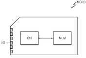
도 1은 본 발명의 실시예에 따른 플래시 메모리 시스템을 나타내는 블록도이고, 도 2는 본 발명의 실시예에 따른 플래시 메모리 시스템에서의 독출 방법을 나타내는 순서도이다.1 is a block diagram illustrating a flash memory system according to an embodiment of the present invention, and FIG. 2 is a flowchart illustrating a read method in a flash memory system according to an embodiment of the present invention.
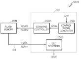
도 1 및 도 2를 참조하면, 본 발명의 실시예에 따른 플래시 메모리 시스템(MSYS)은 플래시 메모리(MEM) 및 컨트롤러(Ctrl)를 구비한다. 그리고 이의 독출 방법은 플래시 메모리(MEM)가 제1 비트 페이지에 대한 하드 데이터(HDTA)를 생성하도록 컨트롤러(Ctrl)로부터 플래시 메모리(MEM)로 제1 독출 명령(RCMD1)을 전송하는 단계(S220) 및 플래시 메모리(MEM)가 제1 비트 페이지에 대한 제1 소프트 데이터(SDTA1)를 생성하도록 컨트롤러(Ctrl)로부터 플래시 메모리(MEM)로 제2 독출 전압의 전압 레벨을 변경한 제1 소프트 독출 전압으로 제2 독출 명령(RCMD2)을 전송하는 단계(S240)를 구비한다.1 and 2, a flash memory system MSYS according to an embodiment of the present invention includes a flash memory MEM and a controller Ctrl. The read method may include transmitting a first read command RCMD1 from the controller Ctrl to the flash memory MEM so that the flash memory MEM generates the hard data HDTA for the first bit page (S220). And the first soft read voltage at which the voltage level of the second read voltage is changed from the controller Ctrl to the flash memory MEM so that the flash memory MEM generates the first soft data SDTA1 for the first bit page. In operation S240, the second read command RCMD2 is transmitted.
본 발명의 실시예에 따른 플래시 메모리 시스템(MSYS)의 플래시 메모리(MEM)는 도 3a에 도시되는 구조의 메모리 셀 어레이(MA)를 포함할 수 있다. 메모리 셀 어레이(MA)는 a(a는 2 이상의 정수)개의 블록들(BLK0~BLKa-1)을 구비하고, 각 블록들(BLK0~BLKa-1)은 b(b는 2 이상의 정수)개의 페이지들(PAG0~PAGb-1)을 구비하며, 각 페이지들(PAG0~PAGb-1)은 c(c는 2 이상의 정수)개의 섹터들(SEC0~SECc-1)을 포함할 수 있다. 도 3a에서는 도시의 편의를 위해, 블록 BLK0에 대하여만 페이지들(PAG0~PAGb-1) 및 섹터들(SEC0~SECc-1)을 도시하였으나, 다른 블록들(BLK1~BLKa-1)도 블록 BLK0와 동일한 구조를 가질 수 있다.The flash memory MEM of the flash memory system MSYS according to the embodiment of the present invention may include a memory cell array MA having the structure shown in FIG. 3A. The memory cell array MA includes a (a is an integer of 2 or more) blocks BLK0 to BLKa-1, and each of the blocks BLK0 to BLKa-1 has b (b is an integer of 2 or more) pages. Fields PAG0 to PAGb-1, each of the pages PAG0 to PAGb-1 may include c (c is an integer of 2 or more) sectors SEC0 to SECC-1. In FIG. 3A, the pages PAG0 to PAGb-1 and the sectors SEC0 to SECC-1 are shown for the block BLK0 only for convenience of illustration, but the other blocks BLK1 to BLKa-1 also block BLK0. It may have the same structure as.
그리고, 본 발명의 실시예에 따른 메모리 셀 어레이(MA)가 낸드 플래시(NAND flash) 메모리의 메모리 셀 어레이인 경우, 도 3a의 블록들(BLK0~BLKa-1)은 각각, 도 3b와 같은 예로 구비될 수 있다. 도 3b를 참조하면, 각 블록들(BLK0~BLKa-1)은 비트 라인(BL0~BLd-1) 방향으로, 8개의 메모리 셀(MCEL)들이 직렬로 연결되는 d(d는 2 이상의 정수)개의 스트링(STR)들로 구비될 수 있다. 각 스트링(STR)은 또한, 각각 직렬로 연결되는 메모리 셀(MCEL)들의 양 끝에 연결되는, 드레인(drain) 선택 트랜지스터(Str1) 및 소스(source) 선택 트랜지스터(Str2)를 포함할 수 있다.When the memory cell array MA according to the embodiment of the present invention is a memory cell array of a NAND flash memory, the blocks BLK0 to BLKa-1 of FIG. 3A may be the same as the example of FIG. 3B. It may be provided. Referring to FIG. 3B, each of the blocks BLK0 to BLKa-1 has a number of d (d is an integer of 2 or more) in which eight memory cells MCEL are connected in series in the bit lines BLO to BLD-1. It may be provided as a string (STR). Each string STR may also include a drain select transistor Str1 and a source select transistor Str2, which are connected to both ends of the memory cells MCEL connected in series, respectively.
도 3b와 같은 구조를 갖는 낸드 플래시 메모리 장치는 블록 단위로 이레이즈가 수행되고, 각 워드 라인(WL0~WL7)에 대응되는 페이지(PAG) 단위로 프로그램을 수행한다. 도 3b는 하나의 블록에 8개의 워드 라인들(WL0~WL7)에 대한 8개의 페이지(PAG)들이 구비되는 예를 도시한다. 다만, 본 발명의 실시예에 따른 메모리 셀 어레이(MA)의 블록들(BLK0~BLKa-1)은 도 3b의 도시되는 메모리 셀(MCEL) 및 페이지(PAG)의 개수와 다른 개수의 메모리 셀 및 페이지를 구비할 수도 있다. 또한, 도 1의 플래시 메모리(MEM)는 이상에서 설명된 메모리 셀 어레이(MA)와 동일한 구조로 동일한 동작을 수행하는 복수개의 메모리 셀 어레이들이 구비될 수도 있다.The NAND flash memory device having the structure as shown in FIG. 3B is erased in units of blocks, and performs a program in units of pages PAG corresponding to each word line WL0 to WL7. 3B shows an example in which eight pages PAG for eight word lines WL0 to WL7 are provided in one block. However, the blocks BLK0 to BLKa-1 of the memory cell array MA according to the embodiment of the present invention may have a different number of memory cells than the number of memory cells MCEL and pages PAG shown in FIG. It may be provided with a page. In addition, the flash memory MEM of FIG. 1 may include a plurality of memory cell arrays that perform the same operation in the same structure as the memory cell array MA described above.
도 3b와 같은 구조의 반도체 메모리 장치의 메모리 셀(MCEL)들은 각각, 프로그램 되어 있는 프로그램 데이터의 비트의 개수에 따라, 도 4와 같은 산포 중 하나의 산포에 포함되는 문턱 전압(Vth)을 가질 수 있다. 도 4의 (a)는 메모리 셀(MCEL)들이 각각 하나의 비트로 프로그램 되는 SLC(Single-Level Cell) 플래시 메모리에서의 셀 산포를 나타내고, 도 4의 (b)는 메모리 셀(MCEL)들이 각각 2 비트로 프로그램 되는 2 비트 MLC(Multi-Level Cell) 플래시 메모리에서의 셀 산포를 나타내며, 도 4의 (c)는 메모리 셀(MCEL)들이 각각 3 비트로 프로그램 되는 3 비트 MLC 플래시 메모리에서의 셀 산포를 나타낸다.Each of the memory cells MCEL of the semiconductor memory device having the structure as shown in FIG. 3B may have a threshold voltage Vth included in one of the distributions as shown in FIG. 4 according to the number of bits of programmed program data. have. FIG. 4A illustrates a cell distribution in a single-level cell (SLC) flash memory in which memory cells MCELs are programmed with one bit, and FIG. 4B illustrates two memory cells MCELs each. 4 shows a cell spread in a 2-bit MLC (multi-level cell) flash memory programmed into bits, and FIG. 4C shows a cell spread in a 3-bit MLC flash memory in which memory cells MCEL are programmed to 3 bits, respectively. .
도 3b의 메모리 셀 어레이(MA)의 메모리 셀(MCEL)들 각각은, 프로그램 된 데이터의 값에 따라, SLC 플래시 메모리의 경우 이레이즈 상태(E) 및 프로그램 상태(P) 중 하나의 상태에 포함되는 문턱 전압을 갖고, 2 비트 MLC 플래시 메모리의 경우 이레이즈 상태(E) 및 제1 프로그램 상태(P1) 내지 제3 프로그램 상태(P3) 중 하나의 상태에 포함되는 문턱 전압을 가지며, 3 비트 MLC 플래시 메모리의 경우 이레이즈 상태(E) 및 제1 프로그램 상태(P1) 내지 제7 프로그램 상태(P7) 중 하나의 상태에 포함되는 문턱 전압을 갖는다.Each of the memory cells MCEL of the memory cell array MA of FIG. 3B is included in one of an erased state E and a program state P in the case of an SLC flash memory according to a value of programmed data. Has a threshold voltage, and in the case of a 2-bit MLC flash memory, has a threshold voltage included in one of an erased state E and one of the first program state P1 to the third program state P3, and a 3-bit MLC The flash memory has a threshold voltage included in one of an erased state E and one of a first program state P1 to a seventh program state P7.
그러나, 이에 한정되는 것은 아니고, 도 3b의 메모리 셀 어레이(MA)의 메모리 셀(MCEL)들 각각은 4 비트 이상으로 프로그램 될 수 있다. 또한, 도 1의 플래시 메모리(MEM)는 서로 다른 개수의 비트로 프로그램 되는 메모리 셀(MCEL)들을 포함할 수도 있다.However, the present invention is not limited thereto, and each of the memory cells MCEL of the memory cell array MA of FIG. 3B may be programmed with 4 bits or more. In addition, the flash memory MEM of FIG. 1 may include memory cells MCEL programmed with different numbers of bits.
도 4의 (a)에서 SLC 플래시 메모리에 대하여 도시하였으나, 본 발명의 실시예에 따른 독출 방법은 MLC 플래시 메모리에서의 독출 방법임을 알려둔다. 따라서, 본 발명의 실시예에 따른 도 1의 플래시 메모리(MEM)는 MLC 플래시 메모리이다. 다만, 전술한 바와 같이, 본 발명의 실시예에 따른 플래시 메모리(MEM)는 SLC 및 MLC를 모두 포함하거나, 서로 다른 개수의 비트로 프로그램 되는 MLC들을 포함할 수도 있다.Although FIG. 4A illustrates the SLC flash memory, the read method according to the embodiment of the present invention is a read method in the MLC flash memory. Accordingly, the flash memory MEM of FIG. 1 according to an embodiment of the present invention is an MLC flash memory. However, as described above, the flash memory MEM according to the embodiment of the present invention may include both SLC and MLC, or may include MLCs programmed with different numbers of bits.
다시 도 1을 참조하면, 플래시 메모리(MEM)는 제1 독출 명령(RCMD1)을 수신한다. 제1 독출 명령(RCMD1)은 프로그램 데이터의 제1 비트의 비트 값을 식별하기 위한 명령으로 제1 비트 페이지에 대한 어드레스 및 제1 비트 페이지에 대한 제1 독출 전압에 대한 정보를 포함한다. 이하에서 설명되는 본 발명의 실시예에 따른 제1 독출 전압은, 프로그램 도중에 프로그램 데이터의 제1 비트의 독출에 사용되는 제1 독출 전압과, 프로그램이 완료된 상태에서 프로그램 데이터의 제1 비트의 독출에 사용되는 제1 독출 전압 중 하나일 수 있다. 이때, 프로그램 데이터의 제1 비트는 LSB(Least Signification Bit)일 수 있다. 양자의 구분이 필요한 때에는, 프로그램 도중에 제1 비트를 독출하기 위해 제1 비트 페이지에 인가되는 제1 독출 전압의 도면 부호는 VIR1이라 하고, 프로그램이 완료된 상태에서 제1 비트를 독출하기 위해 제1 비트 페이지에 인가되는 제1 독출 전압을 VR1이라 하여, 양자를 구분한다.Referring back to FIG. 1, the flash memory MEM receives the first read command RCMD1. The first read command RCMD1 is a command for identifying a bit value of a first bit of program data and includes information about an address for a first bit page and a first read voltage for a first bit page. The first read voltage according to an embodiment of the present invention described below is a first read voltage used for reading a first bit of program data during a program, and a read of the first bit of program data in a state in which the program is completed. It may be one of the first read voltages used. In this case, the first bit of the program data may be a Least Signification Bit (LSB). When the distinction between the two is required, the reference numeral of the first read voltage applied to the first bit page to read the first bit during the program is VIR1, and the first bit to read the first bit in the state where the program is completed. The first read voltage applied to the page is referred to as VR1 to distinguish the two.
이때, 본 발명의 실시예에 따른 프로그램 도중에 수행되는 독출이란 멀티-비트로 프로그램 하는 중 최종 비트(MSB(Most Signification Bit)) 이전의 비트에 대해 프로그램 된 비트 페이지에서 수행되는 독출을 의미한다. 예를 들어, 같은 2 비트 멀티-레벨 셀 플래시 메모리에서, 프로그램 도중에 수행되는 독출에 대해 설명한다. 도 4의 (b)와 같은 2 비트 멀티-레벨 셀 플래시 메모리에서, 프로그램 데이터의 제1 비트는 LSB일 수 있다.In this case, the read performed during the program according to the embodiment of the present invention refers to the read performed on the bit page programmed for the bit before the last bit (MSB (Most Signification Bit)) during programming in multi-bit. For example, a read performed during a program in the same 2-bit multi-level cell flash memory will be described. In the 2-bit multi-level cell flash memory as shown in FIG. 4B, the first bit of the program data may be LSB.
프로그램 도중의 제1 비트 페이지의 각 메모리 셀은, LSB(제1 비트)에 대한 프로그램 상태를 나타내는 도 5의 (a)의 상태 중 하나에 포함되는 상태의 문턱 전압을 가질 수 있다. 즉, 도 5의 (a)와 같이, 제1 페이지의 메모리 셀들은 이레이즈 상태(E) 및 프로그램 상태(P) 중 하나의 상태로 이레이즈 또는 프로그램 된다.Each memory cell of the first bit page during the program may have a threshold voltage of a state included in one of the states of FIG. 5A indicating a program state for the LSB (first bit). That is, as shown in FIG. 5A, the memory cells of the first page are erased or programmed into one of an erased state E and a program state P. FIG.
도 5의 (a)의 이레이즈 상태(E) 및 프로그램 상태(P) 사이의 전압 레벨을 갖는 제1 독출 전압(VIR1)에 의해 프로그램 데이터의 제1 비트가 "0"인지 "1"인지를 식별하기 위해 수행되는 독출이, 본 발명의 실시에에 따른 프로그램 도중에 수행되는 제1 페이지에 대한 독출이다.Whether the first bit of the program data is "0" or "1" is determined by the first read voltage VIR1 having the voltage level between the erased state E and the program state P of FIG. The read performed to identify is the read to the first page performed during the program according to the practice of the present invention.
반면, 본 발명의 실시예에 따른 프로그램이 완료된 상태에서 수행되는 독출이란 멀티-비트로 프로그램 하는 중 최종 비트(MSB(Most Signification Bit))까지 프로그램 된 후에 수행되는 독출을 의미한다. 예를 들어, 도 4의 (b)와 같은 2 비트 멀티-레벨 셀 플래시 메모리에서, 프로그램 데이터의 제1 비트는 LSB이고 제2 비트(최종 비트)는 프로그램 데이터의 MSB일 수 있다.On the other hand, the read performed when the program according to the embodiment of the present invention is completed means a read performed after programming to the last bit (MSB (Most Signification Bit)) during programming in a multi-bit. For example, in a 2-bit multi-level cell flash memory as shown in FIG. 4B, the first bit of program data may be LSB and the second bit (last bit) may be MSB of program data.
이때, 제2 비트(최종 비트)까지 프로그램이 완료된 메모리 셀들 각각은 도 5의 (b)의 상태 중 하나의 상태를 가질 수 있다. 즉, 메모리 셀들은 이레이즈 상태(E), 제1 프로그램 상태(P1), 제2 프로그램 상태(P2) 및 제3 프로그램 상태(P3) 중 하나의 상태에 포함되는 문턱 전압을 가질 수 있다.In this case, each of the memory cells in which the program is completed up to the second bit (the last bit) may have one of the states of FIG. 5B. That is, the memory cells may have a threshold voltage included in one of an erased state E, a first program state P1, a second program state P2, and a third program state P3.
도 5의 (b)에서 제1 프로그램 상태(P1) 및 제2 프로그램 상태(P2) 사이의 전압 레벨을 갖는 제1 독출 전압(VR1)에 의해 프로그램 데이터의 제1 비트가 독출된다. 제1 독출 전압(VR1)에 의해 도 5의 (b)의 이레이즈 상태(E) 및 제1 프로그램 상태(P1)에 속하는 문턱 전압을 갖는 메모리 셀들에 프로그램 된 프로그램 데이터의 제1 비트는 "1"로 식별되고, 제2 프로그램 상태(P2) 및 제3 프로그램 상태(P3)에 속하는 문턱 전압을 갖는 메모리 셀들에 프로그램 된 프로그램 데이터의 제1 비트는 "0"으로 식별될 수 있다. 즉, 제1 독출 전압(VR1)에 의해, 본 발명의 실시예에 따른 프로그램이 완료된 후에 제1 페이지에 대한 독출이 수행된다. 이하에서는 먼저, 본 발명의 실시예에 따른 프로그램 도중에 제1 독출 전압(VIR1)에 의해 제1 비트 페이지에 대해 수행되는 독출 방법에 대하여 알아본다. 다시 도 3b를 참조하면, 고집적화 및 소형화가 플래시 메모리에서의 이슈가 되고 있어, 도 3b의 메모리 셀(MCEL)들 사이의 거리는 줄어들고 있다. 따라서, 동일한 스트링에서의 인접하여 위치하는 메모리 셀들 사이, 또는 동일한 페이지에서의 인접하여 위치하는 메모리 셀들 사이의 커플링(coupling) 현상이 발생할 수 있다. 나아가, 플래시 메모리 시스템의 성능 열화에 의해, 도 5의 (a)의 LSB 페이지의 셀 산포는 도 6의 (a)와 같이 LSB 페이지의 셀 산포가 변경될 수 있다. 이 경우, 프로그램 도중에, 이레이즈 상태(E) 및 프로그램 상태(P)를 제1 독출 전압(VIR1)에 의해 구분할 수 있는 독출 마진이 줄어들 수 있다. 독출 마진이 줄면, 프로그램 도중에 수행되는 독출에서, 이레이즈 상태(E) 및 프로그램 상태(P)가 인접한 영역의 문턱 전압을 갖는 메모리 셀의 LSB 값이 잘못 독출되는 오류가 발생할 수 있다.In FIG. 5B, the first bit of the program data is read by the first read voltage VR1 having the voltage level between the first program state P1 and the second program state P2. The first bit of the program data programmed into the memory cells having the threshold voltage belonging to the erased state E of FIG. 5B and the first program state P1 by the first read voltage VR1 is “1”. A first bit of program data programmed into memory cells identified as ", and having threshold voltages belonging to the second program state P2 and the third program state P3 may be identified as" 0 ". That is, after the program according to the embodiment of the present invention is completed by the first read voltage VR1, the read of the first page is performed. First, a read method performed on a first bit page by a first read voltage VIR1 during a program according to an exemplary embodiment of the present invention will be described. Referring again to FIG. 3B, high integration and miniaturization have become an issue in the flash memory, and the distance between the memory cells MCEL of FIG. 3B is decreasing. Thus, a coupling phenomenon may occur between adjacently located memory cells in the same string or between adjacently located memory cells in the same page. Furthermore, due to performance degradation of the flash memory system, the cell spread of the LSB page of FIG. 5A may be changed as shown in FIG. 6A. In this case, during the program, a read margin that can distinguish the erased state E and the program state P by the first read voltage VIR1 may be reduced. If the read margin is reduced, an error may occur in the read performed during the program, in which the LSB value of the memory cell having the threshold voltage of the erased state E and the program state P adjacent to each other is incorrectly read.
따라서, 프로그램 도중에 수행되는 독출에서, 제1 비트 페이지에 프로그램 된 제1 비트의 비트 값을, 제1 독출 전압(VIR1)에 의해 독출된 비트 값으로 확정하지 못할 수 있다. 이하에서는 본 발명의 실시예에 따른 플래시 메모리 시스템에서 제1 비트 페이지에 대한 제1 독출 명령에 의해 플래시 메모리로부터 출력된 제1 비트 값들에 포함될 수 있는 에러를 정정하여 제1 비트 값을 결정하는 동작에 대하여 설명한다. 이하에서, 제1 비트 페이지에 대한 제1 독출 명령에 의해 플래시 메모리로부터 출력된 데이터를, 제1 비트 페이지에 대한 하드 데이터라 함을 알려둔다.Therefore, in the read performed during the program, the bit value of the first bit programmed in the first bit page may not be determined as the bit value read by the first read voltage VIR1. Hereinafter, an operation of determining a first bit value by correcting an error that may be included in first bit values output from a flash memory by a first read command for a first bit page in a flash memory system according to an exemplary embodiment of the present invention. It demonstrates. Hereinafter, the data output from the flash memory by the first read command for the first bit page will be referred to as hard data for the first bit page.
다시 도 1을 참조하면, 본 발명의 실시예에 따른 플래시 메모리(MEM)는 제1 독출 명령(RCMD1)에 응답하여, 제1 비트 페이지에 대한 하드 데이터(HDTA)를 출력한다. 제1 독출 명령(RCMD1)은 컨트롤러(Ctrl)로부터 전송된다. 컨트롤러(Ctrl)는 플래시 메모리(MEM)로부터 프로그램 데이터를 독출하기 위해 제1 독출 명령(RCMD1) 등의 명령을 플래시 메모리(MEM)로 전송하는 커맨드 제어부(CCON)를 구비한다. 컨트롤러(Ctrl)는 커맨드 제어부(CCON)와 함께, 제어 신호 생성부(CSG) 및 에러 정정 디코더(EDEC)를 구비한다.Referring back to FIG. 1, in response to the first read command RCMD1, the flash memory MEM outputs the hard data HDTA for the first bit page in response to the first read command RCMD1. The first read command RCMD1 is transmitted from the controller Ctrl. The controller Ctrl includes a command control unit CCON for transmitting a command such as the first read command RCMD1 to the flash memory MEM in order to read program data from the flash memory MEM. The controller Ctrl includes a control signal generation unit CSG and an error correction decoder EDEC together with the command control unit CCON.
제어 신호 생성부(CSG)는 플래시 메모리(MEM)와 연결되는 채널(CH)의 채널 정보(CInf)에 대응되는 제어 신호(XCON)를 생성한다. 제어 신호(XCON)는 커맨드 제어부(CCON)로 전송되어 플래시 메모리(MEM)의 독출을 제어하는 기준을 제공한다. 에러 정정 디코더(EDEC)는 프로그램 데이터들 각각의 제1 비트의 비트 값에 대한 에러 정정 부호화를 수행한다. 제어 신호 생성부(CSG) 및 에러 정정 디코더(EDEC)에 대한 보다 자세한 설명은 후술된다.The control signal generator CSG generates the control signal XCON corresponding to the channel information CInf of the channel CH connected to the flash memory MEM. The control signal XCON is transmitted to the command control unit CCON to provide a reference for controlling the reading of the flash memory MEM. The error correction decoder EDEC performs error correction encoding on the bit value of the first bit of each of the program data. The control signal generator CSG and the error correction decoder EDEC will be described in more detail later.
계속해서 도 1을 참조하면, 커맨드 제어부(CCON)는 제1 비트 페이지의 하드 데이터(HDTA)를 독출하기 위해 플래시 메모리(MEM)로 제1 독출 명령(RCMD1)을 전송한 후, 제1 비트 페이지의 제1 소프트 데이터(SDTA1)를 독출하기 위해 제2 독출 전압의 전압 레벨이 변경된 제2 독출 명령(RCMD2)을 플래시 메모리(MEM)로 전송한다. 다만, 이에 한정되는 것은 아니다. 본 발명의 실시에에 따른 플래시 메모리 시스템 및 이의 독출 방법에 의하면, 제2 독출 명령(RCMD2)에 의한 제1 소프트 데이터(SDTA1)를 먼저 독출한 후, 제1 독출 명령(RCMD1)에 의한 하드 데이터(HDTA)를 나중에 독출할 수도 있다.1, the command controller CCON transmits the first read command RCMD1 to the flash memory MEM to read the hard data HDTA of the first bit page, and then the first bit page. In order to read the first soft data SDTA1, the second read command RCMD2 having the changed voltage level of the second read voltage is transmitted to the flash memory MEM. However, the present invention is not limited thereto. According to the flash memory system and the method of reading the same according to the embodiment of the present invention, the first soft data SDTA1 is first read by the second read command RCMD2 and then the hard data is read by the first read command RCMD1. (HDTA) can be read later.
제2 독출 명령(RCMD2)은 프로그램 데이터의 제2 비트를 독출하기 위한 명령이다. 도 5의 (b)를 참조하면, 도 4의 (b)와 같은 2 비트 멀티-레벨 셀 플래시 메모리는, 제2 독출 전압(VR21, VR22)에 의해, 플래시 메모리(MEM)는 메모리 셀의 MSB 값을 메모리 셀의 문턱 전압에 따라 "1" 및 "0" 중 하나로 식별한다. 제2 독출 전압 VR21은 이레이즈 상태(E) 및 제1 프로그램 상태(P1) 사이의 전압 레벨을 가질 수 있다. 그리고 제2 독출 전압 VR22는 제2 프로그램 상태(P2) 및 제3 프로그램 상태(P3) 사이의 전압 레벨을 가질 수 있다.The second read command RCMD2 is a command for reading a second bit of program data. Referring to FIG. 5B, the 2-bit multi-level cell flash memory as shown in FIG. 4B is driven by the second read voltages VR21 and VR22 so that the flash memory MEM is the MSB of the memory cell. The value is identified as one of "1" and "0" according to the threshold voltage of the memory cell. The second read voltage VR21 may have a voltage level between the erased state E and the first program state P1. The second read voltage VR22 may have a voltage level between the second program state P2 and the third program state P3.
본 발명의 실시예에 따른 커맨드 제어부(CCON)는 제2 비트 페이지의 독출에 사용되는 제2 독출 명령(RCMD2)을, 제2 독출 전압(VR21, VR22)의 전압 레벨을 변경하여, 제1 비트 페이지의 제1 소프트 데이터(SDTA1)를 생성하기 위해, 플래시 메모리(MEM)로 전송한다. 이하에서는 2 비트 멀티-레벨 셀 플래시 메모리를 포함하는 플래시 메모리 시스템에서의 본 발명의 실시예에 따른 제1 비트 페이지에 대한 하드 데이터 및 제1 소프트 데이터의 생성에 대하여 좀 더 자세히 설명한다.The command controller CCON according to an exemplary embodiment of the present invention changes the voltage level of the second read voltages VR21 and VR22 to the second read command RCMD2 used to read the second bit page, thereby changing the first bit. The first soft data SDTA1 of the page is transferred to the flash memory MEM. Hereinafter, generation of hard data and first soft data for a first bit page according to an embodiment of the present invention in a flash memory system including a 2-bit multi-level cell flash memory will be described in more detail.
도 7은 본 발명의 실시예에 따른 2 비트 멀티-레벨 셀 플래시 메모리에서 프로그램 도중의 독출 방법에 의한 LSB 페이지의 하드 데이터 및 제1 소프트 데이터를 생성하는 방법을 설명하는 도면이다.FIG. 7 is a diagram illustrating a method of generating hard data and first soft data of an LSB page by a read method during a program in a 2-bit multi-level cell flash memory according to an exemplary embodiment of the present invention.
도 1 및 도 7을 참조하면, 본 발명의 실시예에 따른 플래시 메모리 시스템(MSYS)은 프로그램 도중의 LSB 페이지를 LSB 독출 명령으로 독출하여 LSB 하드 데이터를 생성한다. LSB 페이지는 전술된 제1 비트 페이지이고, LSB 독출 명령은 전술된 제1 독출 명령(RCMD1)이다. 또한, LSB 하드 데이터는 전술된 제1 비트 페이지의 하드 데이터(HDTA)이다. 이하에서는 용어의 일관된 기재를 위해, LSB 페이지, LSB 독출 명령 및 LSB 하드 데이터를 각각, 제1 비트 페이지, 제1 독출 명령 및 제1 비트 페이지의 하드 데이터라 기재한다.1 and 7, a flash memory system MSYS according to an embodiment of the present invention reads an LSB page during a program with an LSB read command to generate LSB hard data. The LSB page is the first bit page described above, and the LSB read command is the first read command RCMD1 described above. Also, the LSB hard data is hard data HDTA of the first bit page described above. In the following description, the LSB page, the LSB read command and the LSB hard data are referred to as hard data of the first bit page, the first read command, and the first bit page, respectively, for a consistent description of terms.
플래시 메모리(MEM)는 제1 독출 명령에 응답하여, 제1 비트 페이지의 하드 데이터(HDTA)를 생성할 수 있다. 제1 독출 전압(VIR1)에 의해 프로그램 도중의 제1 비트 페이지의 각 메모리 셀의 제1 비트의 비트 값이 "1" 또는 "0"으로 센싱된다. 따라서, 제1 비트 페이지의 하드 데이터(HDTA)는 센싱된 "1" 또는 "0"의 조합으로 생성된다.The flash memory MEM may generate hard data HDTA of the first bit page in response to the first read command. The bit value of the first bit of each memory cell of the first bit page during programming is sensed as "1" or "0" by the first read voltage VIR1. Therefore, the hard data HDTA of the first bit page is generated by a combination of sensed "1" or "0".
그리고, 본 발명의 실시예에 따른 플래시 메모리 시스템(MSYS)은 제1 비트 페이지를 MSB 독출 전압의 전압 레벨을 변경한 MSB 독출 명령으로 독출하여, LSB 소프트 데이터를 생성한다. MSB 페이지는 전술된 제2 비트 페이지이고, MSB 독출 명령은 전술된 제2 독출 명령(RCMD2)일 수 있다. 또한, LSB 소프트 데이터는 전술된 프로그램 도중의 제1 비트 페이지의 제1 소프트 데이터(SDTA1)일 수 있고, MSB 독출 명령의 MSB 독출 전압은 도 5의 (b)의 제2 독출 전압(VR21, VR22)일 수 있다. 이하에서는 용어의 일관된 기재를 위해, MLSB 페이지, MSB 독출 명령, MSB 독출 전압 및 LSB 소프트 데이터를 각각, 제2 비트 페이지, 제2 독출 명령, 제2 독출 전압 및 제1 비트 페이지의 제1 소프트 데이터라 기재한다.The flash memory system MSYS according to an embodiment of the present invention reads the first bit page with an MSB read command that has changed the voltage level of the MSB read voltage to generate LSB soft data. The MSB page may be the second bit page described above, and the MSB read command may be the second read command RCMD2 described above. In addition, the LSB soft data may be the first soft data SDTA1 of the first bit page during the program described above, and the MSB read voltage of the MSB read command is the second read voltage VR21 and VR22 of FIG. 5B. May be). Hereinafter, for consistent description of terms, the MLSB page, the MSB read command, the MSB read voltage and the LSB soft data are respectively referred to as a second bit page, a second read command, a second read voltage and a first soft data of the first bit page. It is described.
전술한 바와 같이, MSB 페이지를 독출하기 위한 제2 독출 전압 VR21은 이레이즈 상태(E) 및 제1 프로그램 상태(P1) 사이의 전압 레벨을 가질 수 있다. 그리고 제2 독출 전압 VR22는 제2 프로그램 상태(P2) 및 제3 프로그램 상태(P3) 사이의 전압 레벨을 가질 수 있다.As described above, the second read voltage VR21 for reading the MSB page may have a voltage level between the erased state E and the first program state P1. The second read voltage VR22 may have a voltage level between the second program state P2 and the third program state P3.
그런데, 본 발명의 실시예 따른 플래시 메모리 시스템(MSYS)에서 프로그램 도중의 제1 비트 페이지의 제1 소프트 데이터(SDTA1)를 생성하기 위해 사용되는 제2 독출 명령(RCMD2)의 제1 소프트 독출 전압은, 제2 비트 페이지를 독출하기 위한 제2 독출 명령(RCMD2)의 제2 독출 전압과 상이하다. 본 발명의 실시에에 따른 커맨드 제어부(CCON)는 도 5의 (b)와 같은 전압 레벨을, 도 7과 같이 제1 독출 전압(VIR1)에 근사한 전압 레벨로 변경한 제2 소프트 독출 전압(VR21', VR22')으로 프로그램 도중의 제1 비트 페이지의 제1 소프트 데이터(SDTA1)를 생성한다.However, in the flash memory system MSYS according to the embodiment of the present invention, the first soft read voltage of the second read command RCMD2 used to generate the first soft data SDTA1 of the first bit page during programming is The second read voltage is different from the second read voltage of the second read command RCMD2 for reading the second bit page. The command control unit CCON according to the embodiment of the present invention changes the voltage level as shown in FIG. 5B to a voltage level approximating the first read voltage VIR1 as shown in FIG. 7. VR22 'generates the first soft data SDTA1 of the first bit page during the program.
제1 독출 전압(VIR1)과 제1 소프트 독출 전압 VR21'와의 전압 차이(d1)와, 제1 독출 전압(VIR1)과 제1 소프트 독출 전압 VR22'와의 전압 차이(d2)는 동일하거나 상이할 수 있다. 즉, 제1 소프트 독출 전압(VVR21', VR22')의 개수는 제1 독출 전압(VIR1)의 개수의 2n(n은 자연수) 배수일 수 있는데, 2n개의 제1 소프트 독출 전압(VR21', VR22')은 제1 독출 전압(VIR1)에 대칭 또는 비대칭되도록 전압 레벨이 변경될 수 있다. 제1 독출 전압(VIR1)과 제1 소프트 독출 전압(VR21', VR22') 사이의 전압 차이(d1, d2), 및 전압 차이 d1과 d2의 동일 여부는 제어 신호(XCON)에 포함되는 채널 정보(CInf)에 대응되어 설정될 수 있다. 이에 대한 구체적인 설명은 후술된다.The voltage difference d1 between the first read voltage VIR1 and the first soft read voltage VR21 'and the voltage difference d2 between the first read voltage VIR1 and the first soft read voltage VR22' may be the same or different. have. That is, the number of the first soft read voltages VVR21 'and VR22' may be a multiple of 2n (n is a natural number) of the number of the first read voltages VIR1, and the 2n first soft read voltages VR21 'and VR22 are multiples. ') May change the voltage level to be symmetrical or asymmetrical to the first read voltage VIR1. Voltage differences d1 and d2 between the first read voltage VIR1 and the first soft read voltages VR21 'and VR22', and whether the voltage differences d1 and d2 are equal to each other are included in the control signal XCON. It may be set corresponding to (CInf). Detailed description thereof will be described later.
제1 소프트 독출 전압(VR21', VR22')에 의해 프로그램 도중의 제1 비트 페이지의 각 메모리 셀의 문턱 전압은 도 7과 같이, "1" 또는 "0"으로 센싱된다. 따라서, 프로그램 도중의 제1 비트 페이지의 제1 소프트 데이터(SDTA1)는 도 7의 구간 ① 내지 ④의 문턱 전압에 대해 각각, "11", "10", "00" 및 "01"로 대응되도록 생성된다.The threshold voltages of the memory cells of the first bit page during the program are sensed as "1" or "0" by the first soft read voltages VR21 'and VR22'. Accordingly, the first soft data SDTA1 of the first bit page during the program corresponds to “11”, “10”, “00” and “01” with respect to the threshold voltages of the
도 8은 하드 데이터 및 제1 소프트 데이터에 근거한, 본 발명의 실시예에 따른 제1 비트 페이지에 대한 독출 데이터를 결정하는 방법을 나타내는 순서도이다.8 is a flowchart illustrating a method of determining read data for a first bit page according to an embodiment of the present invention based on hard data and first soft data.
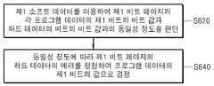
도 1 및 도 8을 참조하면, 도 1의 에러 정정 디코더(EDEC)는 상기와 같이 생성된 제1 소프트 데이터(SDTA1)를 이용하여 프로그램 도중의 제1 비트 페이지의 각 프로그램 데이터의 제1 비트의 비트 값과 하드 데이터의 비트의 비트 값의 동일성 정도를 판단(S820)하고, 그 동일한 정도에 따라 제1 비트 페이지의 하드 데이터(HDTA)의 에러를 정정하여 프로그램 데이터의 제1 비트의 값으로 결정한다(S840).Referring to FIGS. 1 and 8, the error correction decoder EDEC of FIG. 1 uses the first soft data SDTA1 generated as described above to determine the first bit of each program data of the first bit page during the program. The degree of equality between the bit value and the bit value of the bit of the hard data is determined (S820), and the error of the hard data HDTA of the first bit page is corrected according to the same degree to determine the value of the first bit of the program data. (S840).
이상에서는 본 발명의 실시예에 따른 플래시 메모리 시스템(MSYS)에서의 프로그램 도중의 제1 비트 페이지에 대한 독출 방법에 대하여 설명하였다. 본 발명의 실시예에 따른 플래시 메모리 시스템(MSYS)은 프로그램 도중의 제1 비트 페이지에 한하여 하드 데이터 및 제1 소프트 데이터를 생성하고, 이에 근거하여 프로그램 도중의 제1 비트 페이지의 하드 데이터의 에러를 정정함으로써 프로그램 도중의 제1 비트 페이지에 대한 독출을 수행할 수 있다. 다만, 이는 2 비트 멀티-레벨 셀 플래시 메모리 시스템의 경우에 해당하는 사항이다.In the above, the method of reading the first bit page during the program in the flash memory system MSYS according to the exemplary embodiment of the present invention has been described. The flash memory system MSYS according to an embodiment of the present invention generates hard data and first soft data only for a first bit page during a program, and based on this, an error of hard data of a first bit page during a program is detected. By correcting, a read on the first bit page during the program can be performed. However, this is a case of a 2 bit multi-level cell flash memory system.
즉, 본 발명의 실시예에 따른 3 비트 이상의 멀티-레벨 셀 플래시 메모리 시스템에서는 프로그램 도중의 제2 비트 페이지 등도 존재할 수 있다. 이 경우, 프로그램 도중의 제2 비트 페이지 등에 대해서도 소프트 디시젼(soft decision) 동작, 즉 프로그램 도중의 제2 비트 페이지 등에 대한 소프트 데이터에 의해 프로그램 도중의 제2 비트 페이지 등에 대한 하드 데이터의 오류를 정정하는 동작이 수행될 수 있다. 다만, 이하에서는 설명의 편의를 위해 프로그램 도중의 독출에서의 제2 비트 페이지 이상에서의 소프트 디시젼 동작에 대한 설명을 생략한다.That is, in a multi-level cell flash memory system of 3 bits or more according to an embodiment of the present invention, a second bit page during a program may also exist. In this case, a soft decision operation for the second bit page during the program, that is, the error of the hard data for the second bit page during the program is corrected by soft data for the second bit page during the program. An operation may be performed. However, hereinafter, for the convenience of explanation, the description of the soft decision operation on the second bit page or more in reading during the program will be omitted.
본 발명의 실시에에 따른 플래시 메모리 시스템(MSYS)은 프로그램 완료 후의 비트 페이지에 대하여는 소프트 디시젼 동작을 수행하지 아니할 수 있다. 즉, 전술한 바와 같이 프로그램 도중의 비트 페이지에 한하여 소프트 디시젼 동작을 수행할 수 있다. 예를 들어, 2 비트 멀티-레벨 셀 플래시 메모리에서, 도 5의 (b)와 같은 제1 독출 전압(VR1)으로 제1 비트 값을 결정하고 제2 독출 전압(VR21, VR22)으로 제2 비트 값을 결정할 수 있다.The flash memory system MSYS according to an embodiment of the present invention may not perform a soft decision operation on a bit page after program completion. That is, as described above, the soft decision operation can be performed only on the bit page during the program. For example, in a 2-bit multi-level cell flash memory, the first bit value is determined by the first read voltage VR1 as shown in FIG. 5B, and the second bit is determined by the second read voltages VR21 and VR22. The value can be determined.
반면, 본 발명의 실시에에 따른 플래시 메모리 시스템(MSYS)은 프로그램 도중의 비트 페이지에 대한 소프트 디시젼 동작과 별도로 또는 함께, 프로그램 완료 후의 비트 페이지에 대한 소프트 디시젼 동작을 수행할 수 있다. 이때, 프로그램 완료 후의 비트 페이지 중 일부의 비트 페이지에 한하여 소프트 디시젼 동작이 수행될 수 있다. 예를 들어, 2 비트 멀티-레벨 셀 플래시 메모리 시스템에서, 제1 비트 페이지에 대하여만 소프트 디시젼 동작이 수행되고 제2 비트 페이지에 대해서는 그렇지 아니할 수 있다.On the other hand, the flash memory system MSYS according to the embodiment of the present invention may perform the soft decision operation on the bit page after the completion of the program separately or together with the soft decision operation on the bit page during the program. In this case, the soft decision operation may be performed only on the bit pages of the bit pages after the completion of the program. For example, in a 2-bit multi-level cell flash memory system, the soft decision operation may be performed only for the first bit page and not for the second bit page.
이하에서는 프로그램 완료 후의 비트 페이지에 대한 본 발명의 실시예에 따른 다양한 독출 방법에 대하여 설명한다.Hereinafter, various reading methods according to an embodiment of the present invention for a bit page after program completion will be described.
도 9는 본 발명의 실시예에 따른 프로그램 완료 후의 비트 페이지에 대한 독출 방법을 나타내는 순서도이다. 본 발명의 실시예에 따른 프로그램 완료 후의 제1 비트 페이지에 대한 소프트 디시젼 동작은 전술된 도 2에서 설명되었다. 그리고 그 구체적인 동작은 도 5의 (b)의 제1 독출 전압(VR1)에 의해 제1 비트 페이지에 대한 하드 데이터가 독출되는 것을 제외하고는, 도 7 및 도 8에서 설명된 프로그램 도중의 제1 비트 페이지에 대한 사항과 동일하므로, 도 9에서는 프로그램 완료 후의 제1 비트 페이지에 대한 사항은 생략하고 프로그램 완료 후의 제2 비트 페이지에 대한 소프트 디시젼 동작을 설명함을 알려둔다.9 is a flowchart illustrating a reading method of a bit page after completion of a program according to an exemplary embodiment of the present invention. The soft decision operation for the first bit page after program completion according to an embodiment of the present invention has been described in FIG. In addition, the specific operation may include the first method during the program described in FIGS. 7 and 8, except that the hard data for the first bit page is read by the first read voltage VR1 of FIG. 5B. 9, the description of the soft decision operation on the second bit page after the completion of the program is omitted in FIG. 9 since the description on the first bit page after the completion of the program is omitted.
도 1 및 도 9을 참조하면, 본 발명의 실시예에 따른 컨트롤러(Ctrl)의 커맨드 제어부(CCON)는 플래시 메모리(MEM)가 제2 독출 전압으로 제2 비트 페이지에 대한 하드 데이터(HDTA)를 생성하도록, 플래시 메모리(MEM)로 제2 독출 명령(RCMD2)을 전송한다(S820). 제2 독출 명령(RCMD2)은 프로그램 데이터의 제2 비트의 비트 값을 식별하기 위한 명령으로 전술한 바와 같이, 제2 비트 페이지에 대한 어드레스 및 제2 비트 페이지에 대한 독출 전압인 제2 독출 전압에 대한 정보를 포함한다. 또한, 전술한 바와 같이, 도 4의 (b)와 같은 2 비트 멀티-레벨 셀 플래시 메모리에서, 프로그램 데이터의 제2 비트는 프로그램 데이터의 MSB이고, 제2 비트 페이지는 MSB 페이지일 수 있다.1 and 9, the command controller CCON of the controller Ctrl according to an embodiment of the present invention uses the flash memory MEM to read the hard data HDTA for the second bit page as the second read voltage. In operation S820, the second read command RCMD2 is transmitted to the flash memory MEM. The second read command RCMD2 is a command for identifying the bit value of the second bit of the program data. As described above, the second read command RCMD2 is applied to the second read voltage which is an address for the second bit page and a read voltage for the second bit page. Include information about In addition, as described above, in the 2-bit multi-level cell flash memory as shown in FIG. 4B, the second bit of the program data may be an MSB of the program data, and the second bit page may be an MSB page.
도 5의 (b)를 참조하면, 플래시 메모리(MEM)는 제2 독출 전압 VR21에 의해 이레이즈 상태(E)를 "1"인 MSB 값으로 센싱하고, 제1 프로그램 상태(P1) 내지 제3 프로그램 상태(P3)를 "0"인 MSB 값으로 센싱할 수 있다. 그리고, 플래시 메모리(MEM)는 제2 독출 전압 VR22에 의해 이레이즈 상태(E), 제1 프로그램 상태(P1) 및 제2 프로그램 상태(P2)를 "1"인 MSB 값으로 센싱하고, 제1 프로그램 상태(P1) 내지 제3 프로그램 상태(P3)를 "0"인 MSB 값으로 센싱할 수 있다. 이러한 MSB 페이지의 MSB 값들은 MSB 페이지의 하드 데이터(HDTA)로 출력된다.Referring to FIG. 5B, the flash memory MEM senses the erased state E as an MSB value of “1” by the second read voltage VR21, and the first program state P1 to the third. The program state P3 may be sensed as an MSB value of "0". The flash memory MEM senses the erased state E, the first program state P1, and the second program state P2 by the second read voltage VR22 to an MSB value of “1”. The program state P1 to the third program state P3 may be sensed as an MSB value of "0". The MSB values of these MSB pages are output as hard data HDTA of the MSB page.
그런데, 고집적화 또는 플래시 메모리 시스템의 성능 열화에 의해, 도 5의 (b)의 MSB 페이지의 셀 산포가 도 6의 (b)와 같이 변경되어, 제2 독출 전압(VR21, VR22)에 의해 MSB 값을 구분할 수 있는, 독출 마진이 줄어들 수 있다. 독출 마진이 줄면, 이레이즈 상태(E) 및 제1 프로그램 상태(P1)가 인접한 영역의 문턱 전압 또는 제2 프로그램 상태(P2) 및 제3 프로그램 상태(P3)가 인접한 영역의 문턱 전압을 갖는 메모리 셀의 MSB 값이 잘못 독출되는 오류가 발생할 수 있다.However, due to high integration or performance deterioration of the flash memory system, the cell distribution of the MSB page of FIG. 5B is changed as shown in FIG. 6B, and the MSB value is changed by the second read voltages VR21 and VR22. The read margin can be reduced. When the read margin decreases, a memory having an erase voltage E and a first program state P1 having a threshold voltage in an adjacent region or a second program state P2 and a third program state P3 having a threshold voltage in an adjacent region An error may occur in which a cell's MSB value is read incorrectly.
이하에서는 본 발명의 실시예에 따른 플래시 메모리 시스템에서 제2 비트 페이지에 대한 제2 독출 명령에 의해 플래시 메모리로부터 출력된 제2 비트 값들에 포함될 수 있는 에러를 정정하여 제2 비트 값을 결정하는 동작에 대하여 설명한다. 특히, 이하에서는 2 비트 멀티-레벨 셀 플래시 메모리를 포함하는 플래시 메모리 시스템에서의 본 발명의 실시예에 따른 제2 비트 페이지에 대한 하드 데이터 및 제1 소프트 데이터의 생성에 대하여 좀 더 자세히 설명한다. 또한, 전압 레벨이 변경되지 아니한 제2 독출 명령에 의해 제2 비트 페이지에 대해 출력된 데이터를 제2 비트 페이지의 하드 데이터라 하고, 전압 레벨이 변경된 제2 독출 명령에 의해 제2 비트 페이지에 대해 출력된 데이터를 제2 비트 페이지의 제1 소프트 데이터라 함을 알려둔다.Hereinafter, an operation of determining a second bit value by correcting an error that may be included in second bit values output from a flash memory by a second read command for a second bit page in a flash memory system according to an exemplary embodiment of the present invention. It demonstrates. In particular, the generation of hard data and first soft data for a second bit page according to an embodiment of the present invention in a flash memory system including a 2-bit multi-level cell flash memory will be described in more detail. In addition, data output for the second bit page by the second read command in which the voltage level is not changed is called hard data of the second bit page, and data for the second bit page in accordance with the second read command in which the voltage level is changed. Note that the output data is referred to as first soft data of the second bit page.
도 10a는 본 발명의 실시예에 따른 2 비트 멀티-레벨 셀 플래시 메모리에서의 프로그램 완료 후의 독출 방법에 의한 LSB 페이지의 하드 데이터 및 제1 소프트 데이터를 생성하는 방법을 설명하는 도면이고, 도 10b는 본 발명의 실시예에 따른 2 비트 멀티-레벨 셀 플래시 메모리에서의 프로그램 완료 후의 독출 방법에 의한 MSB 페이지의 하드 데이터 및 제1 소프트 데이터를 생성하는 방법을 설명하는 도면이다.FIG. 10A is a diagram illustrating a method of generating hard data and first soft data of an LSB page by a read method after completion of a program in a 2-bit multi-level cell flash memory according to an embodiment of the present invention, and FIG. A diagram for describing a method of generating hard data and first soft data of an MSB page by a read method after completion of a program in a 2-bit multi-level cell flash memory according to an embodiment of the present invention.
도 1 및 도 10a를 참조하면, 본 발명의 실시예에 따른 플래시 메모리 시스템(MSYS)은 도 5의 (b)의 제1 프로그램 상태(P1) 및 제2 프로그램 상태(P2) 사이의 전압 레벨을 갖는 제1 독출 전압(VR1)으로, 프로그램 완료 후의 LSB 페이지에 대한 독출을 수행할 수 있다. 전술한 바와 같이, 프로그램 완료 후의 제1 페이지(LSB 페이지)에 대한 독출 동작은 도 7의 프로그램 도중의 경우와 독출 전압 레벨만 상이하므로, 도 10a에 대한 더 자세한 설명은 생략한다.1 and 10A, a flash memory system MSYS according to an exemplary embodiment of the present invention may determine a voltage level between a first program state P1 and a second program state P2 of FIG. 5B. With the first read voltage VR1 having, the read of the LSB page after the completion of the program can be performed. As described above, since the read operation of the first page (LSB page) after the completion of the program differs only from the read voltage level during the program of FIG. 7, a detailed description of FIG. 10A is omitted.
도 1 및 도 10b를 참조하면, 본 발명의 실시예에 따른 플래시 메모리 시스템(MSYS)은 프로그램 완료 후의 MSB 페이지인 프로그램 데이터의 제2 비트 페이지를 MSB 독출 명령인 제2 독출 명령(RCMD2)으로 독출하여 MSB 하드 데이터를 생성한다. MSB 하드 데이터는 전술된 제2 비트 페이지의 하드 데이터(HDTA)이다. 이하에서는 용어의 일관된 기재를 위해, MSB 하드 데이터를 제2 비트 페이지의 하드 데이터라 기재한다.1 and 10B, a flash memory system MSYS according to an exemplary embodiment of the present invention reads a second bit page of program data, which is an MSB page after program completion, as a second read command RCMD2, which is an MSB read command. To generate MSB hard data. The MSB hard data is the hard data HDTA of the second bit page described above. In the following description, MSB hard data is referred to as hard data of a second bit page for a consistent description of terms.
플래시 메모리(MEM)는 제2 독출 명령(RCMD2)에 응답하여, 제2 비트 페이지의 하드 데이터(HDTA)를 생성할 수 있다. 제2 독출 전압(VR21, VR22)에 의해 제1 비트 페이지의 각 메모리 셀의 비트 값, 즉 프로그램 데이터의 제2 비트의 비트 값이 "1" 또는 "0"으로 센싱된다. 도 10b에서, 제2 독출 전압 VR21보다 문턱 전압이 낮은 셀의 비트 값이 "1"로 센싱되고 제2 독출 전압 VR21 및 VR22 사이의 문턱 전압을 갖는 셀의 비트 값이 "0"으로 센싱되며, 제2 독출 전압 VR22보다 문턱 전압이 큰 셀의 비트 값이 "1"로 센싱되는 예를 도시한다. 상기와 같은 비트 값들로 하드 데이터(HDTA)가 생성되면, 플래시 메모리(MEM)는 제2 비트 페이지에 대한 하드 데이터(HDTA)를 컨트롤러(Ctrl)로 전송한다.The flash memory MEM may generate hard data HDTA of the second bit page in response to the second read command RCMD2. The bit value of each memory cell of the first bit page, that is, the bit value of the second bit of the program data is sensed as "1" or "0" by the second read voltages VR21 and VR22. In FIG. 10B, a bit value of a cell having a threshold voltage lower than the second read voltage VR21 is sensed as "1", and a bit value of a cell having a threshold voltage between the second read voltage VR21 and VR22 is sensed as "0". An example in which a bit value of a cell having a threshold voltage greater than the second read voltage VR22 is sensed as "1" is shown. When the hard data HDTA is generated using the bit values as described above, the flash memory MEM transmits the hard data HDTA for the second bit page to the controller Ctrl.
그리고, 본 발명의 실시예에 따른 플래시 메모리 시스템(MSYS)은 제2 비트 페이지를, 제2 독출 전압(VR21, VR22)의 전압 레벨을 변경하여 MSB 소프트 데이터, 즉 제2 비트 페이지의 제1 소프트 데이터(SDTA1)를 생성한다. 도 5의 (b)와 같이, MSB 페이지를 독출하기 위한 제2 독출 전압 VR21은 이레이즈 상태(E) 및 제1 프로그램 상태(P1) 사이의 전압 레벨을 가질 수 있다. 그리고 제2 독출 전압 VR22는 제2 프로그램 상태(P2) 및 제3 프로그램 상태(P3) 사이의 전압 레벨을 가질 수 있다.In addition, the flash memory system MSYS according to the embodiment of the present invention changes the voltage level of the second bit page and the second read voltages VR21 and VR22 so that the MSB soft data, that is, the first soft page of the second bit page, is changed. Generate the data SDTA1. As shown in FIG. 5B, the second read voltage VR21 for reading the MSB page may have a voltage level between the erased state E and the first program state P1. The second read voltage VR22 may have a voltage level between the second program state P2 and the third program state P3.
그런데, 본 발명의 실시예 따른 플래시 메모리 시스템(MSYS)에서 제2 비트 페이지의 제1 소프트 데이터(SDTA1)를 생성하기 위해 사용되는 제2 독출 명령(RCMD2)의 제2 소프트 독출 전압(VR21', VR22', VR21", VR22")은, 제2 비트 페이지의 하드 데이터(HDTA)를 생성하기 위한 제2 독출 명령(RCMD2)의 제2 독출 전압(VR21, VR22)과 상이하다. 본 발명의 실시에에 따른 커맨드 제어부(CCON)는 제2 비트 페이지의 하드 데이터(HDTA)를 생성하기 위해 사용된 도 10b의 제2 독출 전압(VR21, VR22)의 전압 레벨을 변경한 제2 소프트 독출 전압(VR21', VR22', VR21", VR22")으로 제2 비트 페이지의 제1 소프트 데이터(SDTA1)를 생성한다.However, the second soft read voltage VR21 ′ of the second read command RCMD2 used to generate the first soft data SDTA1 of the second bit page in the flash memory system MSYS according to the embodiment of the present invention. VR22 ', VR21 ", and VR22" are different from the second read voltages VR21 and VR22 of the second read command RCMD2 for generating the hard data HDTA of the second bit page. The command control unit CCON according to an embodiment of the present invention may be configured to change the voltage level of the second read voltages VR21 and VR22 of FIG. 10B used to generate the hard data HDTA of the second bit page. The first soft data SDTA1 of the second bit page is generated using the read voltages VR21 ', VR22', VR21 ", and VR22".
제2 독출 전압 VR21과 제2 소프트 독출 전압 VR21'와의 전압 차이(d1)와, 제2 독출 전압 VR21과 제2 소프트 독출 전압 VR22'와의 전압 차이(d2)는 동일하거나 상이할 수 있다. 마찬가지로, 제2 독출 전압 VR22와 제2 소프트 독출 전압 VR21"와의 전압 차이(d3)와, 제2 독출 전압 VR22과 제2 소프트 독출 전압 VR22"와의 전압 차이(d4)는 동일하거나 상이할 수 있다. 나아가, 제2 독출 전압 VR21과 제2 소프트 독출 전압 VR21' 및 VR22'와의 전압 차이(d1, d2)와, 제2 독출 전압 VR22와 제2 소프트 독출 전압 VR21" 및 VR22"와의 전압 차이(d3, d4)는 동일하거나 상이할 수 있다.The voltage difference d1 between the second read voltage VR21 and the second soft read voltage VR21 'and the voltage difference d2 between the second read voltage VR21 and the second soft read voltage VR22' may be the same or different. Similarly, the voltage difference d3 between the second read voltage VR22 and the second soft read voltage VR21 "and the voltage difference d4 between the second read voltage VR22 and the second soft read voltage VR22" may be the same or different. Furthermore, the voltage difference d1 and d2 between the second read voltage VR21 and the second soft read voltages VR21 'and VR22' and the voltage difference d3 between the second read voltage VR22 and the second soft read voltage VR21 "and VR22". d4) may be the same or different.
제2 소프트 독출 전압(VR21', VR22', VR21", VR22")에 의해 제2 비트 페이지의 각 메모리 셀의 문턱 전압은 도 10과 같이,"1" 또는 "0"으로 센싱된다. 따라서, 제1 비트 페이지의 제1 소프트 데이터(SDTA1)는 도 10b의 구간 ① 내지 ⑦의 문턱 전압에 대해 각각,"11", "10", "00", "01", "00", "10" 및 "11"대응되도록 생성된다. 제2 비트 페이지의 제1 소프트 데이터(SDTA1)를 이용하여 제2 비트 페이지의 각 메모리 셀의 비트 값을 결정하는 방법은 전술된 제1 비트 페이지에 대한 것과 같으므로, 이에 대한 더 자세한 설명은 생략한다.The threshold voltage of each memory cell of the second bit page is sensed as "1" or "0" by the second soft read voltages VR21 ', VR22', VR21 ", and VR22". Accordingly, the first soft data SDTA1 of the first bit page corresponds to "11", "10", "00", "01", "00", and "thresholds" for the threshold voltages of the
도 10b는 제2 비트 페이지의 제1 소프트 데이터(SDTA1)를 생성하기 위해, 제2 비트 페이지의 이레이즈 상태 및 i(i는 2j-1, j는 자연수)개의 프로그램 상태 중 제2 독출 전압(VR21, VR22)으로 식별되는 인접한 모든 상태에 대하여 제2 소프트 독출 전압(VR21', VR22', VR21", VR22")으로 독출되는 예를 도시하였다. 구체적으로, 도 10b는 제2 비트 페이지에 대한 제1 소프트 데이터(SDTA1)를 생성함에 있어, 제2 독출 전압 VR21로 식별되고 서로 인접한 이레이즈 상태(E) 및 제1 프로그램 상태(P1)에 대하는 제2 소프트 독출 전압(VR21', VR22')에 의해 메모리 셀의 문턱 전압이 다시 독출되고, 제2 독출 전압 VR22로 식별되고 서로 인접한 제2 프로그램 상태(P2) 및 제3 프로그램 상태(P3)에 대하여도 제2 소프트 독출 전압(VR21", VR22")에 의해 메모리 셀의 문턱 전압이 다시 독출된다.FIG. 10B illustrates a second read voltage of an erased state of the second bit page and i (i of 2j −1 and j of a natural number) program states for generating the first soft data SDTA1 of the second bit page. An example is shown in which the second soft read voltages VR21 ', VR22', VR21 ", and VR22" are read for all adjacent states identified by (VR21, VR22). Specifically, FIG. 10B illustrates the erase state E and the first program state P1 identified as the second read voltage VR21 and adjacent to each other in generating the first soft data SDTA1 for the second bit page. The threshold voltages of the memory cells are read again by the second soft read voltages VR21 'and VR22', and the second program state P2 and the third program state P3 identified as the second read voltage VR22 and adjacent to each other. The threshold voltage of the memory cell is again read out by the second soft read voltages VR21 "and VR22".
다만, 이에 한정되는 것은 아니다. 도 11과 같이, 제2 독출 전압 VR21로 식별되고 서로 인접한 이레이즈 상태(E) 및 제1 프로그램 상태(P1)에 대하여는 제2 소프트 독출 전압(VR21', VR22')에 의해 제1 소프트 데이터(SDTA1)가 생성되는 반면, 제2 독출 전압 VR22로 식별되고 서로 인접한 제2 프로그램 상태(P2) 및 제3 프로그램 상태(P3)에 대하여는 제2 소프트 독출 전압이 인가되지 아니할 수 있다. 이렇듯 본 발명의 실시예에 따른 플래시 메모리 시스템(MSYS)에 의하면, 프로그램 상태 각각의 변동에 따라 제1 소프트 데이터를 달리 생성함으로써, 플래시 메모리의 성능 열화 특성에 최적화된 독출 동작이 수행될 수 있다.However, the present invention is not limited thereto. As illustrated in FIG. 11, in the erase state E and the first program state P1 identified as the second read voltage VR21 and adjacent to each other, the first soft data (the second soft read voltages VR21 ′ and VR22 ′) is used. While SDTA1) is generated, the second soft read voltage may not be applied to the second program state P2 and the third program state P3 identified as the second read voltage VR22 and adjacent to each other. As described above, according to the flash memory system MSYS according to the exemplary embodiment of the present invention, the first soft data is generated differently according to the change of each program state, so that a read operation optimized for the performance deterioration characteristic of the flash memory may be performed.
또한, 도 10b는 프로그램 완료 후의 제2 비트 페이지에 대한 독출 동작에 한하여 설명되었으나, 본 발명의 실시예에 따른 3 비트 이상의 멀티-레벨 셀 플래시 메모리 시스템에서의 프로그램 도중의 제2 비트 페이지에 대한 독출 동작에도 적용될 수 있음은 당연하다. 다만, 전술한 바와 같이, 프로그램 도중의 제2 독출 전압의 전압 레벨과 도 10b의 프로그램 완료 후의 제2 독출 전압의 전압 레벨을 상이할 것이다.In addition, although FIG. 10B has been described with respect to the read operation for the second bit page after the completion of the program, the read of the second bit page during the program in the multi-level cell flash memory system of three or more bits according to an embodiment of the present invention. Of course, it can be applied to the operation. However, as described above, the voltage level of the second read voltage during the program and the voltage level of the second read voltage after the program completion of FIG. 10B will be different.
이상에서는 본 발명의 실시예에 따른 플래시 메모리 시스템 및 이의 독출 방법을 설명함에 있어, 2 비트 멀티-레벨 셀 플래시 메모리에 대한 예를 들었다. 그러나, 이에 한정되는 것은 아니다. 이하에서는 3 비트 멀티-레벨 셀 플래시 메모리를 포함하는 플래시 메모리 시스템에서의 독출 방법에 대하여 설명한다.In the above description, a flash memory system and a reading method thereof according to an exemplary embodiment of the present invention have been described with reference to a 2-bit multi-level cell flash memory. However, the present invention is not limited thereto. Hereinafter, a method of reading in a flash memory system including a 3-bit multi-level cell flash memory will be described.
도 12는 3 비트 멀티-레벨 셀 플래시 메모리에서의 프로그램 과정을 설명하기 위한 도면이고, 도 13은 3 비트 멀티-레벨 셀 플래시 메모리 시스템을 나타내는 도면이다.FIG. 12 is a diagram for describing a program process in a 3 bit multi-level cell flash memory, and FIG. 13 is a diagram illustrating a 3 bit multi-level cell flash memory system.
3 비트 멀티-레벨 셀 플래시 메모리 시스템에서, 먼저 프로그램 데이터의 제1 비트가 도 12의 (a)의 이레이즈 상태(E) 및 프로그램 상태(P) 중 하나로 프로그램 된다. 이때, 프로그램 도중, 제1 비트 페이지의 프로그램 상태는 제1 독출 전압(VIR1)에 의해 독출된다. 도 12의 (a)의 제1 독출 전압(VIR1)은 도 5의 (a)에서 설명된 제1 독출 전압(VIR1)과 같을 수 있다.In a 3-bit multi-level cell flash memory system, first the first bit of program data is programmed into one of the erased state E and the program state P of FIG. At this time, during the program, the program state of the first bit page is read by the first read voltage VIR1. The first read voltage VIR1 of FIG. 12A may be the same as the first read voltage VIR1 described with reference to FIG. 5A.
도 12의 (a)의 상태로부터 도 12의 (b)의 이레이즈 상태(E) 및 제1 프로그램 상태(P1) 내지 제1 프로그램 상태(P1) 중 하나로 프로그램 된다. 이때, 프로그램 도중, 프로그램 데이터의 제2 비트는 도 12의 (b)에 도시된 제2 독출 전압(VIR21, VIR22)에 의해 독출된다. 도 12의 (a)에 대한 독출이 프로그램 도중에 수행되는 독출임을 나타내기 위하여 도 10a의 프로그램 완료 후의 제1 독출 전압(VR1)과 구분되는 제1 독출 전압(VIR1)으로 도시한 것과 같이, 도 12의 (b)의 제2 독출 전압(VIR21, VIR22) 또한 도 10b의 제2 독출 전압(VR21, VR22)과 다른 도면부호로 도시한다.It is programmed from the state of FIG. 12A to one of the erased state E of FIG. 12B and the first program state P1 to the first program state P1. At this time, during the program, the second bit of the program data is read out by the second read voltages VIR21 and VIR22 shown in Fig. 12B. As shown in FIG. 12A, the first read voltage VIR1 is distinguished from the first read voltage VR1 after the completion of the program of FIG. 10A to indicate that the read is performed during the program. The second read voltages VIR21 and VIR22 in (b) are also shown with different reference numerals than the second read voltages VR21 and VR22 in FIG. 10B.
도 12의 (a)의 상태로부터 도 12의 (c)의 상태로 프로그램 되어, 3 비트 멀티-레벨 셀 플래시 메모리 시스템에서의 프로그램 데이터에 대한 프로그램이 완료된다. 3 비트 멀티-레벨 셀 플래시 메모리 시스템에서의 각 메모리 셀은 도 12의 (c)의 이레이즈 상태(E) 및 제1 프로그램 상태(P1) 내지 제7 프로그램 상태(P7) 중 하나의 상태에 속할 수 있다. 이때, 프로그램 데이터의 제1 비트는 도 12의 (c)의 제1 독출 전압(VR1)에 의해 식별되고, 제2 비트는 도 12의 (c)의 제2 독출 전압(VR21, VR22)에 의해 식별되며, 제3 비트는 제3 독출 전압(VR31, VR32, VR33, VR34)에 의해 식별될 수 있다.Programmed from the state of FIG. 12A to the state of FIG. 12C, the program for the program data in the 3-bit multi-level cell flash memory system is completed. Each memory cell in the 3-bit multi-level cell flash memory system may belong to one of an erased state E and a first program state P1 to a seventh program state P7 of FIG. 12C. Can be. In this case, the first bit of the program data is identified by the first read voltage VR1 of FIG. 12C, and the second bit is identified by the second read voltages VR21 and VR22 of FIG. 12C. The third bit may be identified by the third read voltages VR31, VR32, VR33, and VR34.
플래시 메모리(MEM)는 도 12의 (c)의 제3 프로그램 상태 및 제4 프로그램 상태 사이의 전압 레벨을 갖는 제1 독출 전압(VR1)에 의해, 프로그램 완료 후의 이레이즈 상태, 제1 프로그램 상태 및 제2 프로그램 상태에 속하는 메모리 셀에 프로그램된 프로그램 데이터의 제1 비트를 "1"로 식별하고, 제4 프로그램 상태 내지 제7 프로그램 상태에 속하는 메모리 셀에 프로그램된 프로그램 데이터의 제1 비트를 "0"으로 식별한다. 그리고, 플래시 메모리(MEM)는 각각, 도 12의 (c)의 제1 프로그램 상태 및 제2 프로그램 상태 사이, 및 제5 프로그램 상태 및 제6 프로그램 상태 사이의 전압 레벨을 갖는 제2 독출 전압(VR21, VR22)에 의해 제2 비트의 비트 값을 식별한다.The flash memory MEM is an erased state after completion of a program, a first program state and a first read voltage VR1 having a voltage level between the third and fourth program states of FIG. 12C. A first bit of program data programmed into a memory cell belonging to the second program state is identified as "1", and a first bit of program data programmed into memory cell belonging to the fourth to seventh program states is set to "0". ". Each of the flash memories MEM has a second read voltage VR21 having a voltage level between the first program state and the second program state of FIG. 12C, and between the fifth program state and the sixth program state. VR22) identifies the bit value of the second bit.
도 12의 (c)의 제3 독출 전압(VR31, VR32, VR33, VR34)은 이레이즈 상태(E) 및 제1 프로그램 상태(P1) 사이의 전압 레벨, 제2 프로그램 상태(P2) 및 제3 프로그램 상태(P3) 사이의 전압 레벨, 제4 프로그램 상태(P4) 및 제5 프로그램 상태(P5) 사이의 전압 레벨 및 제6 프로그램 상태(P6) 및 제7 프로그램 상태(P7) 사이의 전압 레벨을 갖도록 설정될 수 있다. 플래시 메모리(MEM)는 제3 독출 전압 VR31보다 작은 문턱 전압을 갖는 프로그램 데이터의 제3 비트는 "1"로 센싱하고, 제3 독출 전압 VR31 및 VR32 사이의 문턱 전압을 갖는 프로그램 데이터의 제3 비트는"0"으로 센싱하며, 제3 독출 전압 VR32 및 VR33 사이의 문턱 전압을 갖는 프로그램 데이터의 제3 비트는 "1"로 싱한다. 또한, 플래시 메모리(MEM)는 제3 독출 전압 VR33 및 VR34 사이의 문턱 전압을 갖는 프로그램 데이터의 제3 비트는 "0"으로 센싱하고, 제3 독출 전압 VR34보다 큰 문턱 전압을 갖는 프로그램 데이터의 제3 비트는 "1"로 센싱한다.The third read voltages VR31, VR32, VR33, and VR34 of FIG. 12C indicate voltage levels between the erased state E and the first program state P1, the second program state P2, and the third program voltage P3. The voltage level between the program state P3, the voltage level between the fourth program state P4 and the fifth program state P5, and the voltage level between the sixth program state P6 and the seventh program state P7. It can be set to have. The flash memory MEM senses a third bit of program data having a threshold voltage smaller than the third read voltage VR31 as "1", and a third bit of program data having a threshold voltage between the third read voltages VR31 and VR32. Is sensed as "0", and the third bit of program data having a threshold voltage between the third read voltages VR32 and VR33 is "1". In addition, the flash memory MEM senses a third bit of the program data having a threshold voltage between the third read voltages VR33 and VR34 as "0", and the third bit of the program data having a threshold voltage greater than the third read voltage VR34. Three bits sense as "1".
이하에서는 설명의 편의를 위해, 프로그램 도중 또는 프로그램 완료 후의 실시예로 분류하여 설명하지 아니한다. 그럼에도, 전술한 바와 같이, 프로그램 도중 또는 프로그램 완료 후의 차이는 독출 전압 레벨의 차이에 있고, 이하에서 설명되는 실시예들이 프로그램 도중 및 프로그램 완료 후 중 어떤 상태에 대해서도 적용될 수 있음은 당연함을 알려둔다.For convenience of explanation, hereinafter, the description will not be made by dividing into embodiments during the program or after the program is completed. Nevertheless, as mentioned above, the difference during the program or after the program completion is in the difference of the read voltage level, and it is understood that the embodiments described below can be applied to any state during the program and after the program completion. .
도 13의 플래시 메모리 시스템(MSYS)은 도 1과 동일하게 구현될 수 있다. 다만, 도 13의 커맨드 제어부(CCON)는 플래시 메모리(MEM)로 제3 독출 명령(RCMD3)을 더 전송하고, 도 13의 플래시 메모리(MEM)는 제3 독출 명령(RCMD3)에 따른 동작을 수행한다. 도 13이 3 비트 멀티-레벨 셀 플래시 메모리 시스템(MSYS)인 경우, 은, 플래시 메모리 시스템(MSYS)은 제2 독출 전압의 전압 레벨을 변경한 제1 소프트 독출 전압으로 LSB 페이지(제1 비트 페이지)의 제1 소프트 데이터를 생성할 수 있다. 그리고, 플래시 메모리 시스템(MSYS)은 CSB 페이지(제2 비트 페이지)의 제1 소프트 데이터를 생성함에 있어, 전술된 도 10b와 같이 제2 비트 페이지의 산포를 식별하기 위한 제2 독출 전압(VR21, VR22)의 전압 레벨을 변경한 제2 소프트 독출 전압(VR21', VR22')으로 제2 비트 페이지를 독출할 수 있다. 또한, 플래시 메모리 시스템(MSYS)은, MSB 페이지(제3 페이지)를 프로그램 함에 있어, 제3 소프트 독출 전압(VR31', V32', V33', V34')으로 제3 비트 페이지를 독출함으로써, 제3 비트 페이지에 대한 제1 소프트 데이터(SDTA1)를 생성할 수 있다.The flash memory system MSYS of FIG. 13 may be implemented in the same manner as in FIG. 1. However, the command controller CCON of FIG. 13 further transmits the third read command RCMD3 to the flash memory MEM, and the flash memory MEM of FIG. 13 performs an operation according to the third read command RCMD3. do. If FIG. 13 is a 3-bit multi-level cell flash memory system MSYS, the flash memory system MSYS is the LSB page (first bit page) with the first soft read voltage that changed the voltage level of the second read voltage. First soft data may be generated. The flash memory system MSYS generates the first soft data of the CSB page (second bit page). As shown in FIG. 10B, the second read voltage VR21, which identifies the dispersion of the second bit page, is used. The second bit page may be read using the second soft read voltages VR21 'and VR22' which have changed the voltage level of the VR22. In addition, in programming the MSB page (third page), the flash memory system MSYS reads the third bit page with the third soft read voltages VR31 ', V32', V33 ', and V34'. First soft data SDTA1 for a 3 bit page may be generated.
이상에서는 하나의 비트 페이지에 대해 하나의 소프트 데이터가 생성되는 예에 한하여 설명되었다. 그러나, 이에 한정되는 것은 아니다. 본 발명의 실시예에 따른 플래시 메모리 시스템은 하나의 비트 페이지에 대한 두 개 이상의 소프트 데이터를 생성함으로써, 독출의 신뢰성을 향상시킬 수 있다. 도 14는 본 발명의 다른 실시예에 따른 플래시 메모리 시스템을 나타내는 블록도이고, 도 15는 도 14에서의 독출 방법을 나타내는 순서도이다. 그리고, 도 16은 도 15의 독출 방법으로 독출되는 예를 설명하기 위한 도면이다.In the above description, only the example in which one soft data is generated for one bit page is described. However, the present invention is not limited thereto. The flash memory system according to the embodiment of the present invention can improve the reliability of reading by generating two or more soft data for one bit page. 14 is a block diagram illustrating a flash memory system according to another exemplary embodiment. FIG. 15 is a flowchart illustrating a read method of FIG. 14. 16 is a view for explaining an example of reading by the reading method of FIG. 15.
도 14 내지 도 16을 참조하면, 본 발명의 다른 실시예에 따른 플래시 메모리 시스템(MSYS)은 도 2의 독출 방법과 마찬가지로, 플래시 메모리(MEM)가 제1 비트 페이지에 대한 하드 데이터(HDTA)를 생성하도록 컨트롤러(Ctrl)로부터 플래시 메모리(MEM)로 제1 독출 명령(RCMD1)을 전송하는 단계(S1520) 및 플래시 메모리(MEM)가 제1 비트 페이지에 대한 제1 소프트 데이터(SDTA1)를 생성하도록 컨트롤러(Ctrl)로부터 플래시 메모리(MEM)로 제2 독출 전압의 전압 레벨을 제2 소프트 독출 전압으로 변경한 제2 독출 명령(RCMD2)을 전송하는 단계(S1540)를 구비한다.14 to 16, in the flash memory system MSYS according to another exemplary embodiment of the present invention, the flash memory MEM stores the hard data HDTA for the first bit page in the same manner as the read method of FIG. 2. Transmitting a first read command RCMD1 from the controller Ctrl to the flash memory MEM to generate (S1520) and causing the flash memory MEM to generate the first soft data SDTA1 for the first bit page. And transmitting a second read command RCMD2 in which the voltage level of the second read voltage is changed to the second soft read voltage from the controller Ctrl to the flash memory MEM (S1540).
나아가, 도 14의 플래시 메모리 시스템(MSYS)에서의 도 15의 독출 방법에 의하면, 제2 독출 전압(VR21, VR22)의 전압 레벨을 재차 변경한 제3 소프트 독출 전압(VR21", VR22")으로 제1 비트 페이지의 제2 소프트 데이터(SDTA2)가 생성되도록, 제2 독출 명령(RCMD2)을 플래시 메모리(MEM)로 재차 전송하는 단계(S1560)를 더 구비한다. 즉, 본 발명의 다른 실시예에 따르면, 제1 비트 페이지에 대하여 한 번의 제1 독출 명령(RCMD1)으로 하드 데이터(HDTA)가 생성되고, 두 번의 제2 독출 명령(RCMD2)으로 각각 제1 소프트 데이터(SDTA1) 및 제2 소프트 데이터(SDTA2)가 생성된다.Further, according to the read method of FIG. 15 in the flash memory system MSYS of FIG. 14, the voltage level of the second read voltages VR21 and VR22 is changed to the third soft read voltages VR21 "and VR22". In operation S1560, the second read command RCMD2 is again transmitted to the flash memory MEM so that the second soft data SDTA2 of the first bit page is generated. That is, according to another embodiment of the present invention, the hard data HDTA is generated with one first read command RCMD1 with respect to the first bit page, and the first soft data with two second read commands RCMD2, respectively. Data SDTA1 and second soft data SDTA2 are generated.
플래시 메모리(MEM)는 두 회에 걸쳐 전압 레벨이 변경된 소프트 독출 전압(VR21', VR22', VR21", VR22")에 의해 제1 비트 페이지의 각 메모리 셀을 도 16와 같이,"1" 또는 "0"으로 센싱한다. 따라서, 제1 비트 페이지의 제2 소프트 데이터(SDTA2)는 도 16의 구간 ① 내지 ⑥의 문턱 전압에 대해 각각,"111", "101", "100", "000", "001" 및 "011"로 대응되도록 생성된다.The flash memory MEM stores each memory cell of the first bit page as "1" or by the soft read voltages VR21 ', VR22', VR21 ", and VR22" whose voltage levels are changed twice. Sense as "0". Accordingly, the second soft data SDTA2 of the first bit page may be “111”, “101”, “100”, “000”, “001”, and “) for the threshold voltages of the
도 16에서는 첫 번째로 전압 레벨이 변경된 제2 소프트 독출 전압(VR21', VR22')에 의해 제1 비트 페이지의 제1 소프트 데이터(SDTA1)가 생성되고, 두 번째로 전압 레벨이 변경된 제3 소프트 독출 전압(VR21", VR22")에 의해 제1 비트 페이지의 제2 소프트 데이터(SDTA2)가 생성되는 예를 도시하였다. 다만, 이에 한정되는 것은 아니다. 도 17에 도시되는 바와 같이, 첫 번째로 전압 레벨이 변경된 제2 소프트 독출 전압(VR21', VR22')에 의해 제1 비트 페이지의 제2 소프트 데이터(SDTA2)가 생성되고, 두 번째로 전압 레벨이 변경된 제3 소프트 독출 전압(VR21", VR22")에 의해 제1 비트 페이지의 제1 소프트 데이터(SDTA1)가 생성될 수도 있다.In FIG. 16, the first soft data SDTA1 of the first bit page is generated by the second soft read voltages VR21 ′ and VR22 ′ in which the voltage level is changed first, and the third soft in which the voltage level is changed second. An example in which the second soft data SDTA2 of the first bit page is generated by the read voltages VR21 "and VR22" is shown. However, the present invention is not limited thereto. As shown in FIG. 17, second soft data SDTA2 of the first bit page is generated by second soft read voltages VR21 ′ and VR22 ′ in which the voltage level is changed first, and secondly, the voltage level. The first soft data SDTA1 of the first bit page may be generated by the changed third soft read voltages VR21 ″ and VR22 ″.
도 18은 도 16의 하드 데이터 및 제1 소프트 데이터에 근거한, 본 발명의 실시예에 따른 제1 비트 페이지에 대한 독출 데이터를 결정하는 방법을 나타내는 순서도이다.FIG. 18 is a flowchart illustrating a method of determining read data for a first bit page according to an embodiment of the present invention based on the hard data and the first soft data of FIG. 16.
도 14 및 도 18을 참조하면, 도 14의 에러 정정 디코더(EDEC)는 상기와 같이 생성된 제2 소프트 데이터(SDTA2)를 이용하여 제1 비트 페이지의 각 프로그램 데이터의 제1 비트의 비트 값과 하드 데이터의 비트의 비트 값의 동일성 정도를 판단(S1820)하고, 그 동일한 정도에 따라 제1 비트 페이지의 하드 데이터(HDTA)의 에러를 정정하여 프로그램 데이터의 제1 비트의 값으로 결정한다(S1840).14 and 18, the error correction decoder EDEC of FIG. 14 uses a bit value of a first bit of each program data of a first bit page using the second soft data SDTA2 generated as described above. The degree of identity of the bit values of the bits of the hard data is determined (S1820), and the error of the hard data HDTA of the first bit page is corrected according to the same degree to determine the value of the first bit of the program data (S1840). ).
이상에서는 제2 독출 명령의 제2 독출 전압의 전압 레벨을 2회에 걸쳐 변경한 제2 소프트 독출 전압에 의해 제1 비트 페이지의 제1 소프트 데이터 및 제2 소프트 데이터를 생성하는 예에 대하여 설명하였다. 제2 비트 페이지 또는 제3 비트 페이지도 이와 마찬가지 방법으로, 제1 소프트 데이터 및 제2 소프트 데이터를 생성할 수 있을 것이다. 예를 들어, 도 9와 같이 MSB 페이지에 대한 제1 소프트 데이터(SDTA1)를 생성한 후, 제2 독출 전압의 전압 레벨을 재차 변경하여 MSB 페이지에 대한 제2 소프트 데이터를 생성할 수도 있다. 따라서, 이에 대한 더 자세한 설명은 생략한다.In the above, the example of generating the first soft data and the second soft data of the first bit page by the second soft read voltage having the voltage level of the second read voltage of the second read command changed twice. . Similarly, the second bit page or the third bit page may generate the first soft data and the second soft data. For example, after generating the first soft data SDTA1 for the MSB page as shown in FIG. 9, the second soft data for the MSB page may be generated by changing the voltage level of the second read voltage again. Therefore, a detailed description thereof will be omitted.
그리고, 본 발명의 다른 실시에에 따르면 독출 전압의 전압 레벨을 다수 변경하여 해당 페이지에 대한 다수의 소프트 데이터를 생성할 수도 있다. 예를 들어, 도 18과 같이 제1 비트 페이지에 대한 제2 소프트 데이터(SDTA2)를 생성한 후, 제2 독출 전압의 전압 레벨을 다시 변경하여 제3 소프트 데이터를 생성할 수도 있다.According to another exemplary embodiment of the present invention, a plurality of soft data for the corresponding page may be generated by changing a plurality of voltage levels of the read voltage. For example, after generating the second soft data SDTA2 for the first bit page as shown in FIG. 18, the third soft data may be generated by changing the voltage level of the second read voltage again.
나아가, 본 발명의 다른 실시에에 따르면 하드 데이터(HDTA), 제1 소프트 데이터(SDTA1) 및 제2 소프트 데이터(SDTA2)가 서로 다른 독출 명령에 의해 생성될 수 있다. 이에 대하여 설명한다.Furthermore, according to another embodiment of the present invention, the hard data HDTA, the first soft data SDTA1 and the second soft data SDTA2 may be generated by different read commands. This will be described.
도 19는 본 발명의 다른 실시예에 따른 플래시 메모리 시스템을 나타내는 블록도이고, 도 20은 도 19에서의 독출 방법을 나타내는 순서도이다. 그리고, 도 21은 도 20의 독출 방법으로 독출되는 예를 설명하기 위한 도면이다.FIG. 19 is a block diagram illustrating a flash memory system according to another exemplary embodiment. FIG. 20 is a flowchart illustrating a read method of FIG. 19. 21 is a diagram for describing an example of reading by the reading method of FIG. 20.
도 19 내지 도 21을 참조하면, 본 발명의 다른 실시예에 따른 플래시 메모리 시스템(MSYS)은 도 15의 독출 방법과 마찬가지로, 플래시 메모리(MEM)가 제1 비트 페이지에 대한 하드 데이터(HDTA)를 생성하도록 컨트롤러(Ctrl)로부터 플래시 메모리(MEM)로 제1 독출 명령(RCMD1)을 전송하는 단계(S2120) 및 플래시 메모리(MEM)가 제1 비트 페이지에 대한 제1 소프트 데이터(SDTA1)를 생성하도록 컨트롤러(Ctrl)로부터 플래시 메모리(MEM)로 제2 독출 전압의 전압 레벨을 제1 소프트 독출 전압(VR21', VR22')으로 변경한 제2 독출 명령(RCMD2)을 전송하는 단계(S2040)를 구비한다.19 to 21, in the flash memory system MSYS according to another embodiment of the present invention, the flash memory MEM stores the hard data HDTA for the first bit page in the same manner as the read method of FIG. 15. Transmitting the first read command RCMD1 from the controller Ctrl to the flash memory MEM to generate (S2120) and the flash memory MEM to generate the first soft data SDTA1 for the first bit page. And transmitting a second read command RCMD2 from which the voltage level of the second read voltage is changed to the first soft read voltages VR21 'and VR22' from the controller Ctrl to the flash memory MEM (S2040). do.
나아가, 도 19의 플래시 메모리 시스템(MSYS)에서의 도 20의 독출 방법에 의하면, 도 12의 (c)와 같은 제3 독출 전압(VR31, VR32, VR33, VR34)의 전압 레벨을 변경한 제2 소프트 독출 전압(VR31', VR32', VR33', VR34')으로 제1 비트 페이지의 제2 소프트 데이터(SDTA2)가 생성되도록, 제3 독출 명령(RCMD3)을 플래시 메모리(MEM)로 재차 전송하는 단계(S2060)를 더 구비한다. 즉, 본 발명의 다른 실시예에 따르면, 제1 비트 페이지에 대하여 한 번의 제1 독출 명령(RCMD1)으로 하드 데이터(HDTA)가 생성되고, 한 번의 제2 독출 명령(RCMD2)으로 제1 소프트 데이터(SDTA1)가 생성되며, 한 번의 제3 독출 명령(RCMD3)으로 제2 소프트 데이터(SDTA2)가 생성된다.Furthermore, according to the reading method of FIG. 20 in the flash memory system MSYS of FIG. 19, the second voltage obtained by changing the voltage levels of the third read voltages VR31, VR32, VR33, and VR34 as shown in FIG. 12C. The third read command RCMD3 is again transmitted to the flash memory MEM so that the second soft data SDTA2 of the first bit page is generated using the soft read voltages VR31 ', VR32', VR33 ', and VR34'. Step S2060 is further provided. That is, according to another embodiment of the present invention, the hard data HDTA is generated with one first read command RCMD1 for the first bit page, and the first soft data with one second read command RCMD2. SDTA1 is generated, and the second soft data SDTA2 is generated with one third read command RCMD3.
플래시 메모리(MEM)는 제1 소프트 독출 전압(VR21', VR22')에 의해 제1 비트 페이지의 각 메모리 셀을 도 21과 같이, "1" 또는 "0"으로 센싱하여 제1 소프트 데이터(SDTA1)를 생성한다. 그리고, 플래시 메모리(MEM)는 제2 소프트 독출 전압(VR31', VR32', VR33', VR34')에 의해 제1 비트 페이지의 각 메모리 셀을 도 21과 같이, "1" 또는 "0"으로 센싱하여 제2 소프트 데이터(SDTA2)를 생성한다. 제1 비트 페이지의 하드 데이터(HDTA), 제1 소프트 데이터(SDTA1) 및 제2 소프트 데이터(SDTA2)는 도 21의 구간 ① 내지 ⑧의 문턱 전압에 대해 각각, "111", "110", "100", "101", "001", "000", "010" 및 "011"에 대응되도록 생성된다.The flash memory MEM senses each memory cell of the first bit page as "1" or "0" by the first soft read voltages VR21 'and VR22', and thus, the first soft data SDTA1. ) The flash memory MEM sets each memory cell of the first bit page to "1" or "0" by the second soft read voltages VR31 ', VR32', VR33 ', and VR34'. After sensing, the second soft data SDTA2 is generated. The hard data HDTA, the first soft data SDTA1, and the second soft data SDTA2 of the first bit page are respectively " 111 ", " 110 ", " 100 "," 101 "," 001 "," 000 "," 010 "and" 011 ".
도 21과 같이 생성된 하드 데이터(HDTA) 및 제2 소프트 데이터(SDTA2)의 동일성 검토에 의한 독출 데이터의 결정은 도 18의 방법과 동일하므로 이에 대한 더 자세한 설명은 생략한다. 도 19의 플래시 메모리의 다른 페이지들에 대한 소프트 데이터의 생성은 전술된 다양한 방법으로 생성될 수도 있다.Determination of the read data by examining the identity of the hard data HDTA and the second soft data SDTA2 generated as shown in FIG. 21 is the same as the method of FIG. 18, and thus a detailed description thereof will be omitted. The generation of soft data for the other pages of the flash memory of FIG. 19 may be generated by the various methods described above.
도 1 또는 도 14를 참조하면, 본 발명의 실시예에 따른 플래시 메모리 시스템(MSYS)에서 제1 소프트 데이터(SDTA1) 또는 제2 소프트 데이터(SDTA2)의 생성을 제어하는 제어 신호(XCON)는, 전술한 바와 같이 채널(CH)의 상태에 대한 채널 정보(CInf)에 근거하여 제어 신호 생성부(CSG)에 의해 생성된다. 예를 들어, 제어 신호 생성부(CSG)는 채널 정보(CInf)에 근거하여, 제1 소프트 데이터(SDTA1)만을 생성할지 또는 제2 소프트 데이터(SDTA2)까지 생성하여 독출의 신뢰성을 더 향상시킬지를 결정하여 이를 제어 신호(XCON)에 반영할 수 있다. 또는 제어 신호 생성부(CSG)는 채널 정보(CInf)에 근거하여, 전술된 도 10 및 도 11의 독출 방법 중 어느 독출 방법에 의하여 독출을 수행할지를 결정하여 이를 제어 신호(XCON)에 반영할 수 있다.1 or 14, the control signal XCON for controlling the generation of the first soft data SDTA1 or the second soft data SDTA2 in the flash memory system MSYS according to the embodiment of the present invention may be described as follows. As described above, the control signal generation unit CSG is generated based on the channel information CInf of the state of the channel CH. For example, the control signal generation unit CSG generates only the first soft data SDTA1 or even the second soft data SDTA2 based on the channel information CInf to further improve the reliability of the readout. It may be determined and reflected in the control signal XCON. Alternatively, the control signal generator CSG may determine which of the read methods of the above-described read method of FIGS. 10 and 11 to perform the read based on the channel information CInf and reflect the result in the control signal XCON. have.
채널 정보(CInf)는 플래시 메모리의 동작 온도, 잡음 정보, 오류 발생 정보, 메모리 셀에 대한 프로그램 횟수 및 프로그램 데이터의 저장 시간 등에 대한 정보일 수 있다. 본 발명의 실시예에 따른 플래시 메모리 시스템(MSYS)에서의 독출 방법은, 상기와 같은 채널 정보(CInf)에 근거하여 제어 신호(XCON)를 생성하기 위해, 도 22와 같이, 채널 정보를 검출하는 단계(S2220) 및 채널 정보에 따라, 제1 비트 페이지를 제1 소프트 독출 전압으로 독출하여 생성되는 제1 소프트 데이터의 생성 여부를 판단하는 단계(S2240)를 구비할 수 있다.The channel information CInf may be information about an operating temperature of the flash memory, noise information, error occurrence information, a program number for the memory cell, a storage time of the program data, and the like. In the read method of the flash memory system MSYS according to the exemplary embodiment of the present invention, in order to generate the control signal XCON based on the channel information CInf as described above, channel information is detected as shown in FIG. 22. In operation S2220 and determining channel information, determining whether to generate first soft data generated by reading the first bit page using the first soft read voltage may be performed (S2240).
본 발명의 실시예에 따른 플래시 메모리 시스템(MSYS)은 도 22의 S2320과 같이 채널 정보(CInf)를 검출하기 위해, 도 23와 같이 채널 검출부(CDEC)를 더 구비할 수 있다. 채널 검출부(CDEC)는 채널(CH)에 연결되어 채널 정보(CInf)를 검출하여, 에러 정정 디코더(EDEC) 및 제어 신호 생성부(CSG)에 전송할 수 있다.The flash memory system MSYS according to the embodiment of the present invention may further include a channel detector CDEC as shown in FIG. 23 to detect channel information CInf as shown in S2320 of FIG. 22. The channel detector CDEC may be connected to the channel CH to detect channel information CInf and transmit the detected channel information CInf to the error correction decoder EDEC and the control signal generator CSG.
에러 정정 디코더(EDEC)는 채널 검출부(CDEC)로부터 전송된 채널 정보(CInf)에 대응되는 인자(factor)로 에러 정정 동작을 수행할 수 있다. 이때, 에러 정정 디코더(EDEC)는 채널 정보(CInf)를 반영하여 디코딩한 결과에 대한 디코딩 정보(DInf)를 제어 신호 생성부(CSG)에 전송할 수 있다. 제어 신호 생성부(CSG)는 채널 정보(CInf) 또는 디코딩 정보(DInf)를 반영하여 제어 신호(XCON)를 생성할 수 있다.The error correction decoder EDEC may perform an error correction operation with a factor corresponding to the channel information CInf transmitted from the channel detector CDEC. In this case, the error correction decoder EDEC may transmit the decoding information DInf regarding the result of decoding by reflecting the channel information CInf to the control signal generator CSG. The control signal generator CSG may generate the control signal XCON by reflecting the channel information CInf or the decoding information DInf.
다만, 이에 한정되는 것은 아니다. 도 24와 같이 본 발명의 실시예에 따른 채널 정보(CInf)는 플래시 메모리 시스템(MSYS)의 외부에서 검출하여, 제어 신호 생성부(CSG)로 전송될 수도 있다. 도 24에는 도시되지 아니하였으나, 외부로부터, 제어 신호 생성부(CSG)로 전송되는 채널 정보(CInf)는 에러 정정 디코더(EDEC)로도 전송될 수 있다. 이 경우, 전술한 바와 같이, 에러 정정 디코더(EDEC)는 채널 정보(CInf)를 반영하여 디코딩한 결과에 대한 디코딩 정보(DInf)를 제어 신호 생성부(CSG)에 전송할 수 있고, 제어 신호 생성부(CSG)는 채널 정보(CInf) 또는 디코딩 정보(DInf)를 반영하여 제어 신호(XCON)를 생성할 수 있다.However, the present invention is not limited thereto. As shown in FIG. 24, the channel information CInf according to the exemplary embodiment of the present invention may be detected outside the flash memory system MSYS and transmitted to the control signal generator CSG. Although not shown in FIG. 24, the channel information CInf transmitted from the outside to the control signal generator CSG may also be transmitted to the error correction decoder EDEC. In this case, as described above, the error correction decoder EDEC may transmit the decoded information DInf of the decoded result by reflecting the channel information CInf to the control signal generator CSG. The CSG may generate the control signal XCON by reflecting the channel information CInf or the decoding information DInf.
이상에서는 본 발명의 실시예에 따른 플래시 메모리 시스템(MSYS)이 채널 정보(CInf)에 근거하여 제어 신호(XCON)를 생성하는 예에 한하여 설명하였다. 그러나, 이에 한정되는 것은 아니다. 본 발명의 다른 실시예에 따른 도 25의 플래시 메모리 시스템(MSYS)은 플래시 메모리 시스템(MSYS)의 성능 정보(PInf)에 응답하여 제어 신호(XCON)를 생성할 수 있다. 플래시 메모리 시스템(MSYS)의 성능 정보(PInf)는 플래시 메모리(MEM)의 집적도 또는 성능 열화에 대한 정보 등일 수 있다. 성능 정보(PInf)는 도 25에 도시된 바와 같이 외부로부터 전송될 수 있다. 또는, 도 25에 도시되지는 아니하였으나, 성능 정보(PInf)는 제어 신호 생성부(CSG) 또는 컨트롤러(Ctrl)의 레지스터(미도시) 등에 저장될 수도 있다.In the above description, only the example in which the flash memory system MSYS generates the control signal XCON based on the channel information CInf has been described. However, the present invention is not limited thereto. According to another embodiment of the present disclosure, the flash memory system MSYS of FIG. 25 may generate a control signal XCON in response to the performance information PInf of the flash memory system MSYS. The performance information PInf of the flash memory system MSYS may be information on the degree of integration or performance degradation of the flash memory MEM. The performance information PInf may be transmitted from the outside as shown in FIG. 25. Alternatively, although not illustrated in FIG. 25, the performance information PInf may be stored in a control signal generation unit CSG or a register (not shown) of the controller Ctrl.
도 26은 본 발명의 다른 실시예에 따른 플래시 메모리 시스템을 나타내는 블록도이다.26 is a block diagram illustrating a flash memory system according to another example embodiment.
도 26을 참조하면, 도 26의 플래시 메모리 시스템(MSYS)은 플래시 메모리(MEM)로부터 전송되는 하드 데이터(HDTA) 및 제1 소프트 데이터(SDTA1)를 버퍼링하는 리드 버퍼(RBUF)를 더 구비한다. 리드 버퍼(RBUF)는 플래시 메모리(MEM)로부터 하드 데이터(HDTA) 및 제1 소프트 데이터(SDTA1)를 수신한 후 소정 시간이 경과된 후에, 하드 데이터(HDTA) 및 제1 소프트 데이터(SDTA1)를 채널 검출부(CDEC)에 전송할 수 있다. 다만, 리드 버퍼(RBUF)는 도 26과 같이 채널 검출부(CDEC)가 구비되지 아니하는 플래시 메모리 시스템(MSYS)에서는 하드 데이터(HDTA) 및 제1 소프트 데이터(SDTA1)를 에러 정정 디코더(EDEC)로 전송할 수도 있다.Referring to FIG. 26, the flash memory system MSYS of FIG. 26 may further include a read buffer RBUF buffering the hard data HDTA and the first soft data SDTA1 transmitted from the flash memory MEM. The read buffer RBUF receives the hard data HDTA and the first soft data SDTA1 after a predetermined time has elapsed after receiving the hard data HDTA and the first soft data SDTA1 from the flash memory MEM. It can be transmitted to the channel detection unit (CDEC). However, the read buffer RBUF uses the hard data HDTA and the first soft data SDTA1 as the error correction decoder EDEC in the flash memory system MSYS in which the channel detector CDEC is not provided as shown in FIG. 26. You can also send.
도 27은 본 발명의 실시예에 따른 컴퓨팅 시스템 장치를 나타내는 블럭도이다.27 is a block diagram illustrating a computing system device according to an exemplary embodiment of the present invention.
본 발명의 실시예에 따른 컴퓨팅 시스템(CSYS)은 버스(BUS)에 전기적으로 연결된 프로세서(CPU), 사용자 인터페이스(UI) 및 플래시 메모리 시스템(MSYS)을 구비한다. 플래시 메모리 시스템(MSYS)은 메모리 컨트롤러(Ctrl) 및 플래시 메모리(MEM)를 포함한다. 플래시 메모리(MEM)에는 프로세서(CPU)에 의해서 처리된 또는 처리될 N-비트 데이터(N은 1 또는 그 보다 큰 정수)가, 메모리 컨트롤러(Ctrl)를 통해, 저장될 것이다. 도 27의 플래시 메모리 시스템(MSYS)은 도 1 등의 플래시 메모리 시스템(MSYS)과 같을 수 있다. 따라서, 컴퓨팅 시스템(CSYS)에 의하면, 부가적인 모듈의 추가 등이 수반되지 아니하고도 간단한 제어로 플래시 메모리 시스템(MSYS)의 독출의 신뢰성을 향상시킬 수 있다.The computing system CSYS according to an embodiment of the present invention includes a processor (CPU), a user interface (UI), and a flash memory system (MSYS) electrically connected to a bus (BUS). The flash memory system MSYS includes a memory controller Ctrl and a flash memory MEM. In the flash memory MEM, N-bit data (N is an integer of 1 or larger) to be processed or to be processed by the processor CPU will be stored through the memory controller Ctrl. The flash memory system MSYS of FIG. 27 may be the same as the flash memory system MSYS of FIG. 1. Therefore, according to the computing system CSYS, the reliability of the read of the flash memory system MSYS can be improved by simple control without the addition of additional modules or the like.
본 발명의 실시예에 따른 컴퓨팅 시스템(CSYS)는 파워 공급 장치(PS)를 더 구비할 수 있다. 또한, 플래시 메모리(MEM)가 도 1 등의 프로그램 방법으로 프로그램을 수행하는 플래시 메모리 장치일 경우, 본 발명의 실시예에 따른 컴퓨팅 시스템(CSYS)은 휘발성 메모리 장치(예를 들어, RAM)을 더 구비할 수 있다.The computing system CSYS according to an embodiment of the present invention may further include a power supply device PS. In addition, when the flash memory MEM is a flash memory device that executes a program by the program method of FIG. It can be provided.
본 발명의 실시예에 따른 컴퓨팅 시스템(CSYS)이 모바일 장치인 경우, 컴퓨팅 시스템의 동작 전압을 공급하기 위한 배터리 및 베이스밴드 칩셋(baseband chipset)과 같은 모뎀이 추가적으로 제공될 수 있다. 또한, 본 발명의 실시예에 따른 컴퓨팅 시스템(CSYS)에는 응용 칩셋(application chipset), 카메라 이미지 프로세서(Camera Image Processor: CIS), 모바일 디램, 등이 더 제공될 수 있음은 이 분야의 통상적인 지식을 습득한 자들에게 자명한 사항인 바, 더 자세한 설명은 생략한다.When the computing system CSYS according to the embodiment of the present invention is a mobile device, a modem such as a battery and a baseband chipset for supplying an operating voltage of the computing system may be additionally provided. In addition, it is common knowledge in the art that an application chipset, a camera image processor (CIS), a mobile DRAM, and the like may be further provided in the computing system CSYS according to the embodiment of the present invention. This is obvious to those who have learned, so a detailed description is omitted.
도 28은 본 발명의 실시예에 따른 메모리 카드를 나타내는 블럭도이다.28 is a block diagram illustrating a memory card according to an embodiment of the present invention.
도 28을 참조하면, 본 발명의 실시예에 따른 메모리 카드(MCRD)는, 메모리 컨트롤러(Ctrl) 및 플래시 메모리(MEM)를 구비한다. 메모리 컨트롤러(Ctrl)는 입출력 수단(I/O)를 통해 수신되는 외부의 호스트(미도시)의 요청에 응답하여 플래시 메모리(MEM)로의 데이터 기입 또는 플래시 메모리(MEM)로부터의 데이터 독출을 제어한다. 또한, 메모리 컨트롤러(Ctrl)는 플래시 메모리(MEM)에 대한 소거 동작을 제어한다. 본 발명의 실시예에 따른 메모리 카드(MCRD)의 메모리 컨트롤러(Ctrl)는 상기와 같은 제어 동작을 수행하기 위해, 각각 호스트 및 메모리 장치와의 인터페이스를 수행하는 인터페이스부들(미도시), 및 램(RAM) 등을 구비할 수 있다. 본 발명의 실시예에 따른 메모리 카드(MCRD)는 도 1 등의 플래시 메모리 시스템(MSYS)으로 구현될 수 있다.Referring to FIG. 28, a memory card MCRD according to an embodiment of the present invention includes a memory controller Ctrl and a flash memory MEM. The memory controller Ctrl controls data writing to or reading data from the flash memory MEM in response to a request from an external host (not shown) received through the input / output means I / O. . Also, the memory controller Ctrl controls the erase operation on the flash memory MEM. The memory controller Ctrl of the memory card MCRD according to an exemplary embodiment of the present invention may include interface units (not shown) and RAM (not shown) for performing an interface with a host and a memory device, respectively, in order to perform the above control operations. RAM) and the like. The memory card MCRD according to the embodiment of the present invention may be implemented with the flash memory system MSYS of FIG. 1.
도 28의 메모리 카드(MCRD)는 컴팩트 플래시 카드(CFC: Compact Flash Card), 마이크로 드라이브(Microdrive), 스마트 미디어 카드(SMC: Smart Media Card) 멀티미디어 카드(MMC: Multimedia Card), 보안 디지털 카드(SDC: Security Digital Card), 메모리 스틱(Memory Stick), 및 USB 플래시 메모리 드라이버 등으로 구현될 수 있다. 따라서, 도 28의 메모리 카드(MCRD)에 의하면, 부가적인 모듈의 추가 등이 수반되지 아니하고도 간단한 제어로 플래시 메모리 시스템(MSYS)의 독출의 신뢰성을 향상시킬 수 있다.The memory card MCRD of FIG. 28 is a compact flash card (CFC: Compact Flash Card), a microdrive (Microdrive), a smart media card (SMC: Smart Media Card), a multimedia card (MMC: Multimedia Card), a secure digital card (SDC). It may be implemented as a security digital card, a memory stick, or a USB flash memory driver. Therefore, according to the memory card MCRD of FIG. 28, the reliability of reading out of the flash memory system MSYS can be improved by simple control without the addition of additional modules or the like.
도 29는 본 발명의 실시예에 따른 솔리드 스테이트 드라이브(SSD: Solid State Drive)를 나타내는 도면이다.29 illustrates a solid state drive (SSD) according to an embodiment of the present invention.
도 29를 참조하면, 본 발명의 실시예에 따른 SSD는 SSD 컨트롤러(SCTL) 및 플래시 메모리(MEM)를 포함한다. SSD 컨트롤러(SCTL)는 버스(BUS)로 연결되는 프로세서(PROS), 램(RAM), 캐쉬 버퍼(CBUF) 및 메모리 컨트롤러(Ctrl)를 구비할 수 있다. 프로세서(PROS)는 호스트(미도시)의 요청(명령, 어드레스, 데이터)에 응답하여 메모리 컨트롤러(Ctrl)가 플래시 메모리(MEM)와 데이터를 송수신하도록 제어한다. 본 발명의 실시예에 따른 SSD의 프로세서(PROS) 및 메모리 컨트롤러(Ctrl)는 하나의 ARM 프로세서로 구현될 수도 있다. 프로세서(PROS)의 동작에 필요한 데이터는 램(RAM)에 로딩될 수 있다.Referring to FIG. 29, an SSD according to an embodiment of the present invention includes an SSD controller SCTL and a flash memory MEM. The SSD controller SCTL may include a processor PROS, a RAM, a cache buffer CBUF, and a memory controller Ctrl connected to a bus BUS. The processor PROS controls the memory controller Ctrl to exchange data with the flash memory MEM in response to a request (command, address, data) of the host (not shown). The processor PROS and the memory controller Ctrl of the SSD according to the embodiment of the present invention may be implemented as one ARM processor. Data necessary for the operation of the processor PROS may be loaded into the RAM.
호스트 인터페이스(HOST I/F)는 호스트의 요청을 수신하여 프로세서(PROS)로 전송하거나, 플래시 메모리(MEM)로부터 전송된 데이터를 호스트로 전송한다. 호스트 인터페이스(HOST I/F)는 USB(Universal Serial Bus), MMC(Man Machine Communication), PCI-E(Peripheral Component Interconnect-Express), SATA(Serial Advanced Technology Attachment), PATA(Parallel Advanced Technology Attachment), SCSI(Small Computer System Interface), ESDI(Enhanced Small Device Interface), 그리고 IDE(Intelligent Drive Electronics) 등과 같은 다양한 인터페이스 프로토콜로, 호스트와 인터페이스 할 수 있다. 플래시 메모리(MEM)로 전송하고자 하거나, 플래시 메모리(MEM)로부터 전송된 데이터는 캐쉬 버퍼(CBUF)에 임시로 저장될 수 있다. 캐쉬 버퍼(CBUF)는 SRAM 등일 수 있다.The host interface HOST I / F receives a request from the host and transmits the request to the processor PROS or transmits data transmitted from the flash memory MEM to the host. Host interfaces (HOST I / F) include Universal Serial Bus (USB), Man Machine Communication (MMC), Peripheral Component Interconnect-Express (PCI-E), Serial Advanced Technology Attachment (SATA), Parallel Advanced Technology Attachment (PATA), Various interface protocols, such as Small Computer System Interface (SCSI), Enhanced Small Device Interface (ESDI), and Intelligent Drive Electronics (IDE), can interface with the host. Data to be transferred to the flash memory MEM or data transferred from the flash memory MEM may be temporarily stored in the cache buffer CBUF. The cache buffer CBUF may be an SRAM or the like.
본 발명의 실시예에 따른 SSD는 도 1 등의 플래시 메모리 시스템(MSYS)으로 구현될 수 있다. 따라서, 도 29의 SSD에 의하면, 부가적인 모듈의 추가 등이 수반되지 아니하고도 간단한 제어로 플래시 메모리 시스템(MSYS)의 독출의 신뢰성을 향상시킬 수 있다.The SSD according to the embodiment of the present invention may be implemented by the flash memory system MSYS of FIG. 1. Therefore, according to the SSD of FIG. 29, the reliability of reading the flash memory system MSYS can be improved by simple control without the addition of additional modules or the like.
도 30은 SSD를 포함하는 서버 시스템 및 네트워크 시스템을 나타내는 도면이다.30 is a diagram illustrating a server system and a network system including an SSD.
도 30을 참조하면, 본 발명의 실시예에 따른 네트워크 시스템(NSYS)은 네트워크를 통해 연결되는 서버 시스템(SSYS) 및 다수의 단말들(TEM1~TEMn)을 포함할 수 있다. 본 발명의 실시예에 따른 서버 시스템(SSYS)은 네트워크에 연결되는 다수의 단말들(TEM1~TEMn)로부터 수신되는 요청을 처리하는 서버(SERVER) 및 단말들(TEM1~TEMn)로부터 수신되는 요청에 대응되는 데이터를 저장하는 SSD를 포함하는 구비할 수 있다. 이때, 도 30의 SSD는 도 29의 SSD일 수 있다. 즉, 도 30의 SSD는 SSD 컨트롤러(SCTL) 및 플래시 메모리(MEM)를 포함하고, 플래시 메모리(MEM)는 도 1 등의 프로그램 방법으로 프로그램을 수행하는 플래시 메모리 장치일 수 있다.Referring to FIG. 30, a network system NSYS according to an embodiment of the present invention may include a server system SSYS and a plurality of terminals TEM1 to TEMn connected through a network. The server system SSYS according to an embodiment of the present invention responds to a request received from a server SERVER and terminals TEM1 to TEMn processing a request received from a plurality of terminals TEM1 to TEMn connected to a network. And an SSD for storing corresponding data. In this case, the SSD of FIG. 30 may be the SSD of FIG. 29. That is, the SSD of FIG. 30 may include an SSD controller SCTL and a flash memory MEM, and the flash memory MEM may be a flash memory device that performs a program by the program method of FIG. 1.
이상에서와 같이 도면과 명세서에서 최적 실시예가 개시되었다. 여기서 특정한 용어들이었으나, 이는 단지 본 발명을 설명하기 위한 목적에서 사용된 것이지 의미 한정이나 특허청구범위에 기재된 본 발명의 범위를 제한하기 위하여 사용된 것은 아니다.As described above, optimal embodiments have been disclosed in the drawings and the specification. Although specific terms are employed herein, they are used for purposes of describing the present invention only and are not used to limit the scope of the present invention.
예를 들어, 본 발명의 다른 실시예에 따른 플래시 메모리 시스템에서 제1 비트 페이지에 대한 제1 소프트 데이터 또는 제2 소프트 데이터를 생성하는 방법과 제2 비트 페이지에 대한 제1 소프트 데이터 또는 제2 소프트 데이터를 생성하는 방법이 상이할 수 있다. 또한 4 비트 이상의 프로그램 데이터로 프로그램 되는 메모리 셀을 포함하는 플래시 메모리 시스템에서도 전술된 각 비트 페이지의 제1 소프트 데이터 또는 제2 소프트 데이터를 생성하는 방법이 적용될 수 있을 것이다. 그러므로 본 기술분야의 통상의 지식을 가진 자라면 이로부터 다양한 변형 및 균등한 타 실시예가 가능하다는 점을 이해할 것이다. 따라서, 본 발명의 진정한 기술적 보호범위는 첨부된 특허청구범위의 기술적 사상에 의해 정해져야 할 것이다.For example, a method of generating first soft data or second soft data for a first bit page and a first soft data or second soft for a second bit page in a flash memory system according to another embodiment of the present invention. The method of generating the data may be different. In addition, the above-described method of generating the first soft data or the second soft data of each bit page may be applied to a flash memory system including memory cells programmed with four or more bits of program data. Therefore, those skilled in the art will appreciate that various modifications and equivalent embodiments are possible without departing from the scope of the present invention. Accordingly, the true scope of the present invention should be determined by the technical idea of the appended claims.
Claims (11)
Translated fromKorean상기 프로그램 데이터들 각각의 제1 비트를 프로그램 한 제1 비트 페이지에 대한 제1 독출 전압으로 상기 제1 비트 페이지의 하드 데이터가 생성되도록, 상기 컨트롤러로부터 상기 플래시 메모리로 상기 제1 비트 페이지에 대한 제1 독출 명령을 전송하는 단계; 및
상기 프로그램 데이터들 각각의 제2 비트를 프로그램 한 제2 비트 페이지에 대한 제2 독출 전압의 전압 레벨을 변경한 제1 소프트 독출 전압으로 상기 제1 비트 페이지의 제1 소프트 데이터가 생성되도록, 상기 제2 비트 페이지에 대한 제2 독출 명령을 상기 컨트롤러로부터 상기 플래시 메모리로 전송하는 단계를 구비하는 것을 특징으로 하는 독출 방법.A read method in a flash memory system having a flash memory including memory cells programmed with at least two bits of program data and a controller for controlling the flash memory.
A first read for the first bit page from the controller to the flash memory such that hard data of the first bit page is generated with a first read voltage for the first bit page programmed with the first bit of each of the program data. 1 transmitting a read command; And
The first soft data of the first bit page is generated with a first soft read voltage having a voltage level of a second read voltage for a second bit page programmed with a second bit of each of the program data. And sending a second read command for a two bit page from the controller to the flash memory.
상기 프로그램 데이터의 MSB(Most Signification Bit)에 대한 프로그램이 완료되기 이전의, 프로그램 수행 도중의 제1 비트 페이지에 대한 독출 전압인 것을 특징으로 하는 독출 방법.The method of claim 1, wherein the first read voltage,
And a read voltage for the first bit page during program execution before the program for the MSB (Most Signification Bit) of the program data is completed.
상기 제1 독출 명령은 상기 프로그램 데이터들 각각의 LSB(Least Signification Bit)에 대한 LSB 페이지를 독출하는 독출 명령이고,
상기 제2 독출 명령은 상기 프로그램 데이터들 각각의 MSB에 대한 MSB 페이지를 독출하는 독출 명령인 것을 특징으로 하는 독출 방법.The method according to claim 1,
The first read command is a read command that reads an LSB page for a LSB (Least Signification Bit) of each of the program data.
And the second read command is a read command for reading an MSB page for an MSB of each of the program data.
상기 제1 독출 명령은 상기 프로그램 데이터들 각각의 LSB에 대한 LSB 페이지를 독출하는 독출 명령이고, 상기 제2 독출 명령은 상기 프로그램 데이터들 각각의 CSB 에 대한 CSB 페이지를 독출하는 독출 명령이거나,
상기 제1 독출 명령은 상기 프로그램 데이터들 각각의 CSB에 대한 CSB 페이지를 독출하는 명령이고, 상기 제2 독출 명령은 상기 프로그램 데이터들 각각의 MSB에 대한 MSB 페이지를 독출하는 명령인 것을 특징으로 하는 독출 방법.The method according to claim 1,
The first read command is a read command for reading an LSB page for each LSB of the program data, and the second read command is a read command for reading a CSB page for each CSB of the program data,
The first read command is a command for reading a CSB page for each CSB of the program data, and the second read command is a command for reading an MSB page for an MSB of each of the program data. How to read.
상기 제2 독출 전압의 전압 레벨을 재차 변경한 제2 소프트 독출 전압으로 상기 제1 비트 페이지의 제2 소프트 데이터가 생성되도록, 상기 제2 독출 명령을 상기 플래시 메모리로 재차 전송하는 단계를 더 구비하는 것을 특징으로 하는 독출 방법.The method according to claim 1,
Retransmitting the second read command to the flash memory such that the second soft data of the first bit page is generated with a second soft read voltage that has changed the voltage level of the second read voltage again. Read method, characterized in that.
상기 프로그램 데이터들 각각의 제3 비트를 프로그램 한 제3 비트 페이지에 대한 제3 독출 전압의 전압 레벨을 변경한 제2 소프트 독출 전압으로 상기 제1 비트 페이지의 제2 소프트 데이터가 생성되도록, 상기 제3 비트 페이지에 대한 제3 독출 명령을 상기 컨트롤러로부터 상기 플래시 메모리로 전송하는 단계를 더 구비하는 것을 특징으로 하는 독출 방법.The method according to claim 1,
The second soft data of the first bit page is generated with a second soft read voltage having a voltage level of a third read voltage for a third bit page programmed with a third bit of each of the program data. And sending a third read command for a three bit page from the controller to the flash memory.
상기 제1 독출 전압보다 2n(n은 자연수) 배수만큼 많고, 상기 제1 독출 전압에 대해 대칭 또는 비대칭되는 것을 특징으로 하는 독출 방법.The method of claim 1, wherein the voltage level of the first soft read voltage is
And a reading of 2n (n is a natural number) multiple of the first read voltage and symmetrical or asymmetrical with respect to the first read voltage.
상기 컨트롤러와 상기 플래시 메모리 사이의 채널 상태에 대한 채널 정보 및 상기 플래시 메모리 시스템의 성능에 대한 성능 정보 중 적어도 하나 이상의 정보를 포함하는 소프트 디시젼 신호에 응답하여 수행되는 것을 특징으로 하는 독출 방법.The method of claim 1, wherein the reading method is
And a soft decision signal including at least one of channel information on a channel state between the controller and the flash memory and performance information on the performance of the flash memory system.
상기 제2 독출 전압으로 상기 제2 비트 페이지에 대한 하드 데이터가 생성되도록 상기 컨트롤러로부터 상기 플래시 메모리로 상기 제2 독출 명령을 전송하는 단계; 및
상기 제2 독출 전압의 전압 레벨을 변경한 제2 소프트 독출 전압으로 상기 제2 비트 페이지의 제1 소프트 데이터가 생성되도록, 상기 제2 독출 명령을 상기 컨트롤러로부터 상기 플래시 메모리로 재차 전송하는 단계를 구비하는 것을 특징으로 하는 독출 방법.The method according to claim 1,
Transmitting the second read command from the controller to the flash memory such that hard data for the second bit page is generated at the second read voltage; And
Retransmitting the second read command from the controller to the flash memory such that the first soft data of the second bit page is generated with a second soft read voltage that has changed the voltage level of the second read voltage. Read method, characterized in that.
상기 하드 데이터와 상기 제1 소프트 데이터의 동일한 정도를 판단한 결과에 따라, 상기 하드 데이터를 에러 정정하여 독출 데이터를 결정하는 단계를 더 구비하는 것을 특징으로 하는 독출 방법.The method according to claim 1,
And determining read data by error correcting the hard data according to a result of determining the same degree of the hard data and the first soft data.
상기 플래시 메모리에 프로그램 된 상기 프로그램 데이터의 독출을 제어하는 컨트롤러를 구비하는 플래시 메모리 시스템에 있어서,
상기 컨트롤러는,
상기 플래시 메모리와 연결되는 채널의 채널 정보 또는 상기 플래시 메모리 시스템의 성능 정보에 대응되는 제어 신호를 생성하는 제어 신호 생성부;
상기 제어 신호에 응답하여, 상기 프로그램 데이터들 각각의 제1 비트를 프로그램 한 제1 비트 페이지에 대한 제1 독출 전압으로 상기 제1 비트 페이지의 하드 데이터가 생성되도록 상기 플래시 메모리로 상기 제1 비트 페이지에 대한 제1 독출 명령을 전송하고, 상기 프로그램 데이터들 각각의 제2 비트를 프로그램 한 제2 비트 페이지에 대한 제2 독출 전압의 전압 레벨을 변경한 제2 소프트 독출 전압으로 상기 제1 비트 페이지의 제1 소프트 데이터가 생성되도록, 상기 제2 비트 페이지에 대한 제2 독출 명령을 상기 플래시 메모리로 전송하는 커맨드 제어부; 및
상기 제1 소프트 데이터에 따라, 상기 프로그램 데이터들 각각의 제1 비트의 비트 값이 대응되는 상기 하드 데이터의 비트의 비트 값과 어느 정도 동일한지를 판단하여, 상기 프로그램 데이터들 각각의 제1 비트의 비트 값에 대한 에러 정정 부호화를 수행하는 에러 정정 디코더를 구비하는 것을 특징으로 하는 플래시 메모리 시스템.A flash memory in which each of the at least one page of memory cells is programmed with at least two bits of program data; And
A flash memory system comprising a controller for controlling reading of the program data programmed into the flash memory.
The controller,
A control signal generator configured to generate a control signal corresponding to channel information of a channel connected to the flash memory or performance information of the flash memory system;
In response to the control signal, the first bit page to the flash memory such that hard data of the first bit page is generated at a first read voltage for a first bit page programmed with a first bit of each of the program data. Transmits a first read command for and changes a voltage level of a second read voltage for a second bit page programmed with a second bit of each of the program data to a second soft read voltage of the first bit page. A command controller which transmits a second read command for the second bit page to the flash memory so that first soft data is generated; And
According to the first soft data, it is determined whether or not the bit value of the first bit of each of the program data is equal to the bit value of the bit of the corresponding hard data to determine the bit value of the first bit of each of the program data. And an error correction decoder for performing error correction encoding on the value.
Priority Applications (2)
| Application Number | Priority Date | Filing Date | Title |
|---|---|---|---|
| KR1020110093641AKR20130030099A (en) | 2011-09-16 | 2011-09-16 | Flash memory device and reading method of flash memory device |
| US13/618,336US9001587B2 (en) | 2011-09-16 | 2012-09-14 | Flash memory and reading method of flash memory |
Applications Claiming Priority (1)
| Application Number | Priority Date | Filing Date | Title |
|---|---|---|---|
| KR1020110093641AKR20130030099A (en) | 2011-09-16 | 2011-09-16 | Flash memory device and reading method of flash memory device |
Publications (1)
| Publication Number | Publication Date |
|---|---|
| KR20130030099Atrue KR20130030099A (en) | 2013-03-26 |
Family
ID=48179798
Family Applications (1)
| Application Number | Title | Priority Date | Filing Date |
|---|---|---|---|
| KR1020110093641AAbandonedKR20130030099A (en) | 2011-09-16 | 2011-09-16 | Flash memory device and reading method of flash memory device |
Country Status (1)
| Country | Link |
|---|---|
| KR (1) | KR20130030099A (en) |
Cited By (6)
| Publication number | Priority date | Publication date | Assignee | Title |
|---|---|---|---|---|
| KR20140086369A (en)* | 2012-12-28 | 2014-07-08 | 삼성전자주식회사 | A method of operating MLC memory device and MLC memory device |
| KR101429184B1 (en)* | 2013-09-12 | 2014-08-12 | 주식회사 디에이아이오 | Method of adjusting read voltages for a nand flash memory device |
| US9230638B1 (en) | 2014-10-16 | 2016-01-05 | SK Hynix Inc. | Semiconductor memory device including plurality of memory cells and method of operating the same |
| US9959938B2 (en) | 2015-03-31 | 2018-05-01 | SK Hynix Inc. | Semiconductor memory device outputting status fail signal and operating method thereof |
| US10223011B2 (en) | 2016-04-14 | 2019-03-05 | Samsung Electronics Co., Ltd. | Storage device including nonvolatile memory device and controller and operating method of the storage device |
| KR20210016598A (en)* | 2014-08-19 | 2021-02-16 | 삼성전자주식회사 | Memory devices and modules |
- 2011
- 2011-09-16KRKR1020110093641Apatent/KR20130030099A/ennot_activeAbandoned
Cited By (8)
| Publication number | Priority date | Publication date | Assignee | Title |
|---|---|---|---|---|
| KR20140086369A (en)* | 2012-12-28 | 2014-07-08 | 삼성전자주식회사 | A method of operating MLC memory device and MLC memory device |
| KR101429184B1 (en)* | 2013-09-12 | 2014-08-12 | 주식회사 디에이아이오 | Method of adjusting read voltages for a nand flash memory device |
| WO2015037817A1 (en)* | 2013-09-12 | 2015-03-19 | 주식회사 디에이아이오 | Method for regulating reading voltage of nand flash memory device |
| US9558816B2 (en) | 2013-09-12 | 2017-01-31 | The-Aio Inc. | Method for regulating reading voltage of NAND flash memory device |
| KR20210016598A (en)* | 2014-08-19 | 2021-02-16 | 삼성전자주식회사 | Memory devices and modules |
| US9230638B1 (en) | 2014-10-16 | 2016-01-05 | SK Hynix Inc. | Semiconductor memory device including plurality of memory cells and method of operating the same |
| US9959938B2 (en) | 2015-03-31 | 2018-05-01 | SK Hynix Inc. | Semiconductor memory device outputting status fail signal and operating method thereof |
| US10223011B2 (en) | 2016-04-14 | 2019-03-05 | Samsung Electronics Co., Ltd. | Storage device including nonvolatile memory device and controller and operating method of the storage device |
Similar Documents
| Publication | Publication Date | Title |
|---|---|---|
| KR101835605B1 (en) | Flash memory device and reading method of flash memory device | |
| US11740970B2 (en) | Dynamic adjustment of data integrity operations of a memory system based on error rate classification | |
| US9858996B2 (en) | Memory access module for performing sensing operations on storage cells of a storage device to obtain soft information and executing a program mode to control access to the storage device | |
| US8479083B2 (en) | Flash memory devices having multi-bit memory cells therein with improved read reliability | |
| US9001587B2 (en) | Flash memory and reading method of flash memory | |
| US11302375B2 (en) | Performing an on demand refresh operation of a memory sub-system | |
| KR101944793B1 (en) | Flash memory system including flash memory and detecting method of abnormal wordline thereof | |
| TWI756603B (en) | Physical unclonable function with nand memory array | |
| US9478298B2 (en) | Memory system and method of reading data thereof | |
| US11023177B2 (en) | Temperature correction in memory sub-systems | |
| US8923067B2 (en) | Memory system and method of operating memory system using soft read voltages | |
| US20150043282A1 (en) | Method of estimating deterioration state of memory device and related method of wear leveling | |
| KR20130084901A (en) | Flash memory device and reading method of flash memory device | |
| KR102089570B1 (en) | Storage device and data processing method thereof | |
| US11726869B2 (en) | Performing error control operation on memory component for garbage collection | |
| KR20130087935A (en) | Memory, memory system, and error checking/correction method for memory | |
| US10658065B2 (en) | Failure mode detection method and error correction method for solid state storage device | |
| KR20090099265A (en) | Memory device and data determination method | |
| US12373109B2 (en) | Validating read level voltage in memory devices | |
| KR20120046846A (en) | Flash memory device having flag cells and program operating method thereof | |
| KR20150068137A (en) | Non-volatile memory device and operation method thereof | |
| KR20130030099A (en) | Flash memory device and reading method of flash memory device | |
| KR20180026022A (en) | Storage device and copy-back method thereof | |
| KR20130102397A (en) | Flash memory and reading method of flash memory | |
| US20250004645A1 (en) | Copyback clear command for performing a scan and read in a memory device |
Legal Events
| Date | Code | Title | Description |
|---|---|---|---|
| PA0109 | Patent application | Patent event code:PA01091R01D Comment text:Patent Application Patent event date:20110916 | |
| PG1501 | Laying open of application | ||
| A201 | Request for examination | ||
| PA0201 | Request for examination | Patent event code:PA02012R01D Patent event date:20160919 Comment text:Request for Examination of Application Patent event code:PA02011R01I Patent event date:20110916 Comment text:Patent Application | |
| E902 | Notification of reason for refusal | ||
| PE0902 | Notice of grounds for rejection | Comment text:Notification of reason for refusal Patent event date:20170720 Patent event code:PE09021S01D | |
| E701 | Decision to grant or registration of patent right | ||
| PE0701 | Decision of registration | Patent event code:PE07011S01D Comment text:Decision to Grant Registration Patent event date:20180126 | |
| PC1904 | Unpaid initial registration fee |