KR20130024163A - Liquid crystal display device including substrate having emitting device attached thereon - Google Patents
Liquid crystal display device including substrate having emitting device attached thereonDownload PDFInfo
- Publication number
- KR20130024163A KR20130024163AKR1020110087422AKR20110087422AKR20130024163AKR 20130024163 AKR20130024163 AKR 20130024163AKR 1020110087422 AKR1020110087422 AKR 1020110087422AKR 20110087422 AKR20110087422 AKR 20110087422AKR 20130024163 AKR20130024163 AKR 20130024163A
- Authority
- KR
- South Korea
- Prior art keywords
- liquid crystal
- substrate
- crystal panel
- light
- guide plate
- Prior art date
- Legal status (The legal status is an assumption and is not a legal conclusion. Google has not performed a legal analysis and makes no representation as to the accuracy of the status listed.)
- Withdrawn
Links
Images


Classifications
- G—PHYSICS
- G02—OPTICS
- G02F—OPTICAL DEVICES OR ARRANGEMENTS FOR THE CONTROL OF LIGHT BY MODIFICATION OF THE OPTICAL PROPERTIES OF THE MEDIA OF THE ELEMENTS INVOLVED THEREIN; NON-LINEAR OPTICS; FREQUENCY-CHANGING OF LIGHT; OPTICAL LOGIC ELEMENTS; OPTICAL ANALOGUE/DIGITAL CONVERTERS
- G02F1/00—Devices or arrangements for the control of the intensity, colour, phase, polarisation or direction of light arriving from an independent light source, e.g. switching, gating or modulating; Non-linear optics
- G02F1/01—Devices or arrangements for the control of the intensity, colour, phase, polarisation or direction of light arriving from an independent light source, e.g. switching, gating or modulating; Non-linear optics for the control of the intensity, phase, polarisation or colour
- G02F1/13—Devices or arrangements for the control of the intensity, colour, phase, polarisation or direction of light arriving from an independent light source, e.g. switching, gating or modulating; Non-linear optics for the control of the intensity, phase, polarisation or colour based on liquid crystals, e.g. single liquid crystal display cells
- G02F1/133—Constructional arrangements; Operation of liquid crystal cells; Circuit arrangements
- G02F1/1333—Constructional arrangements; Manufacturing methods
- G02F1/1335—Structural association of cells with optical devices, e.g. polarisers or reflectors
- G02F1/1336—Illuminating devices
- G—PHYSICS
- G02—OPTICS
- G02F—OPTICAL DEVICES OR ARRANGEMENTS FOR THE CONTROL OF LIGHT BY MODIFICATION OF THE OPTICAL PROPERTIES OF THE MEDIA OF THE ELEMENTS INVOLVED THEREIN; NON-LINEAR OPTICS; FREQUENCY-CHANGING OF LIGHT; OPTICAL LOGIC ELEMENTS; OPTICAL ANALOGUE/DIGITAL CONVERTERS
- G02F1/00—Devices or arrangements for the control of the intensity, colour, phase, polarisation or direction of light arriving from an independent light source, e.g. switching, gating or modulating; Non-linear optics
- G02F1/01—Devices or arrangements for the control of the intensity, colour, phase, polarisation or direction of light arriving from an independent light source, e.g. switching, gating or modulating; Non-linear optics for the control of the intensity, phase, polarisation or colour
- G02F1/13—Devices or arrangements for the control of the intensity, colour, phase, polarisation or direction of light arriving from an independent light source, e.g. switching, gating or modulating; Non-linear optics for the control of the intensity, phase, polarisation or colour based on liquid crystals, e.g. single liquid crystal display cells
- G02F1/133—Constructional arrangements; Operation of liquid crystal cells; Circuit arrangements
- G02F1/1333—Constructional arrangements; Manufacturing methods
- G02F1/1335—Structural association of cells with optical devices, e.g. polarisers or reflectors
- G02F1/133524—Light-guides, e.g. fibre-optic bundles, louvered or jalousie light-guides
- G—PHYSICS
- G02—OPTICS
- G02F—OPTICAL DEVICES OR ARRANGEMENTS FOR THE CONTROL OF LIGHT BY MODIFICATION OF THE OPTICAL PROPERTIES OF THE MEDIA OF THE ELEMENTS INVOLVED THEREIN; NON-LINEAR OPTICS; FREQUENCY-CHANGING OF LIGHT; OPTICAL LOGIC ELEMENTS; OPTICAL ANALOGUE/DIGITAL CONVERTERS
- G02F1/00—Devices or arrangements for the control of the intensity, colour, phase, polarisation or direction of light arriving from an independent light source, e.g. switching, gating or modulating; Non-linear optics
- G02F1/01—Devices or arrangements for the control of the intensity, colour, phase, polarisation or direction of light arriving from an independent light source, e.g. switching, gating or modulating; Non-linear optics for the control of the intensity, phase, polarisation or colour
- G02F1/13—Devices or arrangements for the control of the intensity, colour, phase, polarisation or direction of light arriving from an independent light source, e.g. switching, gating or modulating; Non-linear optics for the control of the intensity, phase, polarisation or colour based on liquid crystals, e.g. single liquid crystal display cells
- G02F1/133—Constructional arrangements; Operation of liquid crystal cells; Circuit arrangements
- G02F1/1333—Constructional arrangements; Manufacturing methods
- G02F1/1335—Structural association of cells with optical devices, e.g. polarisers or reflectors
- G02F1/133553—Reflecting elements
Landscapes
- Physics & Mathematics (AREA)
- Nonlinear Science (AREA)
- Mathematical Physics (AREA)
- Chemical & Material Sciences (AREA)
- Crystallography & Structural Chemistry (AREA)
- General Physics & Mathematics (AREA)
- Optics & Photonics (AREA)
- Liquid Crystal (AREA)
Abstract
Translated fromKoreanDescription
Translated fromKorean본 발명은 액정표시소자에 관한 것으로, 특히 광원인 LED이 액정패널의 기판상에 실장되어 면적을 최소화할 수 있는 액정표시소자에 관한 것이다.The present invention relates to a liquid crystal display device, and more particularly, to a liquid crystal display device in which an LED, which is a light source, is mounted on a substrate of a liquid crystal panel to minimize an area thereof.
근래, 핸드폰(Mobile Phone), PDA, 노트북컴퓨터와 같은 각종 휴대용 전자기기가 발전함에 따라 이에 적용할 수 있는 경박단소용의 평판표시장치(Flat Panel Display Device)에 대한 요구가 점차 증대되고 있다. 이러한 평판표시장치로는 LCD(Liquid Crystal Display)나 PDP(Plasma Display Panel), 유기전계발광 표시소자 등이 활발히 연구되었지만, 양산화 기술, 구동수단의 용이성, 고화질의 구현, 대면적 화면의 실현이라는 이유로 인해 현재에는 액정표시소자(LCD)가 주로 각광을 받고 있다.2. Description of the Related Art Recently, various portable electronic devices such as a mobile phone, a PDA, and a notebook computer have been developed. Accordingly, there is a growing need for a flat panel display device for a light and small size. Although such liquid crystal displays (LCDs), plasma display panels (PDPs), and organic light emitting display devices have been actively studied, such flat panel displays are based on mass production technology, ease of driving means, high definition, and large screen realization. As a result, liquid crystal displays (LCDs) are mainly in the spotlight.
상기 액정표시소자는 투과형 표시소자로서, 액정분자의 굴절률 이방성에 의해 액정층을 투과하는 광의 양을 조절함으로써 원하는 화상을 화면상에 표시한다. 따라서, 액정표시소자에서는 화상의 표시를 위해 액정층을 투과하는 광원인 백라이트장치(back light unit)가 설치된다. 일반적으로 백라이트장치는 크게 2종류로 구분될 수 있다.The liquid crystal display element is a transmissive display element and displays a desired image on the screen by adjusting the amount of light transmitted through the liquid crystal layer by refractive index anisotropy of liquid crystal molecules. Therefore, in the liquid crystal display device, a back light unit, which is a light source that transmits the liquid crystal layer, is provided for displaying an image. In general, the backlight device may be classified into two types.
첫째는 램프가 액정패널의 측면에 설치되어 액정층에 광을 제공하는 측면형 백라이트장치이고 둘째는 램프가 액정패널의 하부에서 직접 광을 제공하는 직하형 백라이트장치이다.First is a side type backlight device in which a lamp is provided on the side of the liquid crystal panel to provide light to the liquid crystal layer, and second is a direct type backlight device in which the lamp provides light directly from the lower part of the liquid crystal panel.
측면형 백라이트장치는 액정패널의 측면에 설치되어 반사판과 도광판을 통해 액정층을 광을 공급할 수 있다. 따라서, 두께를 얇게 할 수 있게 되므로, 얇은 두께의 표시장치가 요구되는 노트북 등에 주로 사용된다. 그러나, 측면형 백라이트장치는 광을 발광하는 램프가 액정패널의 측면에 위치하므로 대면적의 액정패널에 적용하기 어려울 뿐만 아니라 도광판을 통해 광이 공급되므로 고휘도를 얻기 어렵게 된다. 따라서, 근래 각광받고 있는 대면적의 LCD TV용 액정패널에는 적합하지 않다는 문제가 있었다.The side type backlight device may be installed on the side of the liquid crystal panel to supply light to the liquid crystal layer through the reflection plate and the light guide plate. Therefore, since the thickness can be made thinner, it is mainly used for a notebook or the like requiring a thin display device. However, in the side type backlight device, since a lamp emitting light is located on the side of the liquid crystal panel, it is difficult to apply to a large area liquid crystal panel and light is supplied through the light guide plate, thereby making it difficult to obtain high brightness. Therefore, there has been a problem in that it is not suitable for large-area liquid crystal panel for LCD TV, which has recently been spotlighted.
직하형 백라이트장치는 램프로부터 발광된 광이 직접 액정층에 공급되므로 대면적의 액정패널에 적용될 수 있을 뿐만 아니라 고휘도가 가능하기 때문에, 근래 LCD TV용 액정패널을 제작하는데 주로 사용되고 있다.The direct type backlight device is not only applied to a large area liquid crystal panel because the light emitted from the lamp is directly supplied to the liquid crystal layer, so that high brightness is possible.
한편, 근래 백라이트장치의 광원으로서 형광램프 대신 발광소자(Light Emitting Device)와 같이 자체적으로 광을 발광하는 광원을 사용하고 있다. 이 발광소자는 R, G, B 단색광을 방출하기 때문에, 백라이트장치에 적용했을 때 색재현율이 좋고 구동전력을 절감할 수 있다는 장점이 있다.On the other hand, in recent years, as a light source of a backlight device, a light source that emits light itself, such as a light emitting device, is used instead of a fluorescent lamp. Since the light emitting device emits R, G, and B monochromatic light, it has an advantage of good color reproduction and reduction of driving power when applied to a backlight device.
도 1은 상기와 같은 발광소자를 구비한 백라이트장치가 설치된 종래 액정표시소자의 구조를 간략하게 나타내는 단면도이다.1 is a cross-sectional view briefly showing the structure of a conventional liquid crystal display device provided with a backlight device having the light emitting device as described above.
도 1에 도시된 바와 같이, 액정표시소자는 제1기판(11) 및 제2기판(13)과 그 사이의 액정층(도면표시하지 않음)으로 이루어져 외부로부터 신호가 인가됨에 따라 화상을 구현하는 액정패널(10)과, 상기 액정패널(10)의 하부 일측면 또는 양측면에 배치되어 광을 발광하는 LED(Light Emitting Device;52)가 실장된 LED부(50)와, 상기 액정패널(10)의 하부에 배치되어 LED(52)에서 발광된 광을 인도하여 상기 액정패널(10)로 공급하는 도광판(20)과, 상기 액정패널(10)과 도광판(20) 사이에 구비되어 도광판(20)에서 인도되어 액정패널(10)로 공급되는 광을 확산하고 집광하여 광의 효율을 향상시키는 광학시트(30)와, 상기 도광판(20) 하부에 배치되어 하부로 입력되는 광을 상기 액정패널(10)로 반사시키는 반사판(27)과, 상기 도광판(20)과 및 액정패널(10)을 지지하는 메인지지부(25)와, 상기 메인지지부(25)와 결합되어 액정패널(10), 도광판(20), 광학시트(30)를 조립하는 하부커버(40) 및 상부커버(42)로 구성된다.As shown in FIG. 1, the liquid crystal display device includes a
도면에는 도시하지 않았지만, 액정패널(10)의 제1기판(1)에는 복수의 화소가 구비되어 있으며, 각각의 화소에는 화소전극 및 박막트랜지스터가 형성되어 있고 제2기판(3)에는 공통전극이 형성되어 있어서, 상기 박막트랜지스터를 통해 외부로부터 신호가 인가되는 경우 액정층에 전계가 형성되어 액정분자의 배향을 조절하여 상기 액정층을 투과하는 광의 투과량을 조절함으로써 화상을 구현한다. 이때, 제1기판(1) 및 제2기판(3)에는 각각 편광판(도면표시하지 않음)이 부착되어 액정층으로 입사되는 광 및 액정층에서 출력되는 광의 편광방향을 제어한다.Although not shown in the drawing, the first substrate 1 of the
그러나, 상기와 같은 구성의 액정표시소자에서는 다음과 같은 문제가 발생하는데, 이를 설명하면 다음과 같다.However, the following problems occur in the liquid crystal display device having the above configuration, which will be described below.
도면에는 자세히 도시하지 않았지만, 상기 LED부(50)는 LED기판과 상기 LED기판에 형성된 배선으로 이루어져 있으며, LED(52)가 상기 LED기판에 실장되어 각종 배선을 통해 신호가 인가됨으로써 LED(52)가 발광하게 된다. 따라서, LED기판 등의 구성 등에 의해 LED부(50)가 차지하는 영역이 증가하게 되는데, 이러한 영역의 증가는 액정표시소자의 면적 증가를 야기할 뿐만 아니라, 베젤(bezzel)의 크기가 증가하게 되는 문제가 있었다.Although not shown in detail in the drawing, the
본 발명은 상기한 문제를 해결하기 위한 것으로, LED가 차지하는 공간을 최소화하여 베젤의 면적을 최소화할 수 있는 액정표시소자를 제공하는 것을 목적으로 한다.An object of the present invention is to provide a liquid crystal display device that can minimize the area of the bezel by minimizing the space occupied by the LED.
상기한 목적을 달성하기 위해, 본 발명에 따른 액정표시소자는 액정패널; 상기 액정패널 하부에 배치된 도광판; 상기 도광판 상부의 액정패널에 부착되어 도광판의 상면을 통해 광을 입사시켜 액정패널에 광을 공급하는 복수의 LED패키지로 구성된다.In order to achieve the above object, the liquid crystal display device according to the present invention comprises a liquid crystal panel; A light guide plate disposed under the liquid crystal panel; It is attached to the liquid crystal panel of the upper light guide plate is composed of a plurality of LED packages for supplying light to the liquid crystal panel by injecting light through the upper surface of the light guide plate.
상기 액정패널에는 LED패키지가 부착되는 도전패턴이 형성되어 LED패키지에 신호를 인가하는데, 상기 도전패턴은 금속으로 이루어지고 상기 LED패키지는 전도성 수지에 의해 도전패턴에 부착된다.A conductive pattern to which the LED package is attached is formed on the liquid crystal panel to apply a signal to the LED package. The conductive pattern is made of metal and the LED package is attached to the conductive pattern by a conductive resin.
상기 제1기판 및 제2기판에는 각각 더미영역이 형성되어 제1기판의 더미영역에는 게이트라인 및 데이터라인과 접속되는 패드가 형성되고 제2기판의 더미영역에는 복수의 LED패키지가 부착되는 도전패턴이 형성될 수 있다.A conductive pattern in which a dummy region is formed in each of the first and second substrates, pads connected to gate lines and data lines are formed in the dummy region of the first substrate, and a plurality of LED packages are attached to the dummy region of the second substrate. This can be formed.
또한, 상기 제1기판에는 제1더미영역과 제2더미영역이 형성되어 제1더미영역에는 복수의 LED패키지가 부착되는 도전패턴이 형성되고 제2더미영역에는 게이트라인 및 데이터라인과 접속되는 패드가 형성되어 외부로부터 신호가 액정패널로 인가될 수 있다.In addition, a first dummy region and a second dummy region are formed in the first substrate, and a conductive pattern is formed in the first dummy region to which a plurality of LED packages are attached, and a pad connected to the gate line and the data line in the second dummy region. May be formed to apply a signal from the outside to the liquid crystal panel.
본 발명에서는 LED패키지를 도광판의 측면에 형성하지 않고 액정패널의 하부에 부착함으로써 LED패키지가 차지하는 공간을 최소화하며, 그 결과 액정표시소자의 베젤의 면적을 최소화하여 액정표시소자 면적을 감소시킬 수 있게 된다.The present invention minimizes the space occupied by the LED package by attaching the LED package to the lower portion of the liquid crystal panel without forming the LED package on the side of the light guide plate. As a result, the area of the bezel of the liquid crystal display device can be minimized to reduce the area of the liquid crystal display device. do.
도 1은 종래 액정표시소자의 구조를 나타내는 단면도.
도 2는 본 발명에 따른 액정표시소자의 구조를 나타내는 단면도.
도 3a는 본 발명에 따른 액정패널의 정면도.
도 3b는 본 발명에 따른 액정패널의 배면도.
도 4는 본 발명에 따른 액정패널의 다른 구조를 나타내는 정면도.
도 5는 본 발명에 따른 액정표시소자에 사용된 LED패키지의 구조를 나타내는 단면도.1 is a cross-sectional view showing the structure of a conventional liquid crystal display device.
2 is a cross-sectional view showing the structure of a liquid crystal display device according to the present invention;
3A is a front view of a liquid crystal panel according to the present invention.
Figure 3b is a rear view of the liquid crystal panel according to the present invention.
4 is a front view showing another structure of the liquid crystal panel according to the present invention.
5 is a cross-sectional view showing the structure of the LED package used in the liquid crystal display device according to the present invention.
이하, 첨부한 도면을 참조하여 본 발명에 따른 액정표시소자에 대해 상세히 설명한다.Hereinafter, a liquid crystal display device according to the present invention will be described in detail with reference to the accompanying drawings.
본 발명에서는 별도의 LED기판을 구비하지 않고, LED를 액정패널의 기판에 부착함으로서 LED를 장착하기 위한 공간을 최소화하여 액정표시소자의 베젤을 최소화한다.In the present invention, there is no separate LED substrate, and by attaching the LED to the substrate of the liquid crystal panel, the space for mounting the LED is minimized to minimize the bezel of the liquid crystal display device.
상기 LED는 액정패널의 박막트랜지스터 어레이기판 또는 컬러필터기판의 더미영역에 형성되며, 이때 상기 더미영역에는 도전패턴이 형성되고 이 도전패턴상에 LED패키지가 실장되어 LED에 신호가 인가됨으로써 LED가 발광하게 된다.The LED is formed in a dummy region of a thin film transistor array substrate or a color filter substrate of a liquid crystal panel. In this case, a conductive pattern is formed in the dummy region, and an LED package is mounted on the conductive pattern so that the LED emits light. Done.
도 2는 본 발명에 따른 액정표시소자의 구조를 나타내는 도면이다.2 is a view showing the structure of a liquid crystal display device according to the present invention.
도 2에 도시된 바와 같이, 액정표시소자는 크게 화상을 구현하는 액정패널(110)과, 상기 액정패널(110)에 광을 공급하는 백라이트로 이루어진다.As shown in FIG. 2, the liquid crystal display device includes a liquid crystal panel 110 for largely implementing an image and a backlight for supplying light to the liquid crystal panel 110.
액정패널(110)은 유리와 같은 투명한 물질로 이루어진 제1기판(111) 및 제2기판(113), 상기 제1기판(111)과 제2기판(113) 사이에 배치된 액정층(도면표시하지 않음)으로 이루어진다.The liquid crystal panel 110 includes a
도면에는 도시하지 않았지만, 상기 제1기판(111)에는 종횡으로 배열되어 복수의 화소영역을 정의하는 복수의 게이트라인과 데이터라인이 형성되어 있으며, 각각의 화소영역에는 스위칭소자인 박막트랜지스터가 형성되고 상기 화소영역 위에는 형성된 화소전극이 형성된다. 또한, 상기 박막트랜지스터는 게이트라인과 접속되는 게이트전극, 상기 게이트전극 위에 비정질실리콘 등이 적층되어 형성되는 반도체층, 상기 반도체층 위에 형성되고 데이터라인 및 화소전극에 연결되는 소스전극 및 드레인전극으로 이루어진다.Although not shown in the drawing, a plurality of gate lines and data lines are formed on the
제2기판(113)은 적(Red; R), 녹(Green; G) 및 청(Blue; B)의 색상을 구현하는 다수의 서브-컬러필터로 구성된 컬러필터, 상기 서브-컬러필터 사이를 구분하고 액정층을 투과하는 광을 차단하는 블랙매트릭스(black matrix), 그리고 상기 액정층에 전압을 인가하는 투명한 공통전극으로 이루어져 있다.The
이와 같이 구성된 제1기판(111) 및 제2기판(113)은 화상표시 영역의 외곽에 형성된 실런트(sealant)(미도시)에 의해 대향하도록 합착되어 액정패널을 구성하며, 상기 제1기판(111)과 제2기판(113)의 합착은 상기 제1기판(111) 또는 제2기판(113)에 형성된 합착키(미도시)를 통해 이루어진다.The
한편, 액정패널(110)이 상기와 같이 제1기판(111)에 화소전극이 형성되고 제2기판(113)에 공통전극이 형성되어 액정층에 제1기판(111)의 표면과 수직인 전계를 인가하는 TN모드(Twisted Nematic mode)일 수도 있고, 공통전극과 화소전극이 제1기판(111)에 서로 평행하게 형성되어 액정층에 제1기판(111)의 표면과 수평인 전계를 인가하는 IPS모드(In-Plane Switching mode)일 수도 있다.Meanwhile, the liquid crystal panel 110 has a pixel electrode formed on the
상기 제1기판(111) 및 제2기판(113)에는 각각 제1편광판(116) 및 제2편광판(118)이 부착되어 액정패널(110)로 입력되고 출력되는 광을 편광시켜 화상을 구현한다.A first
상기 제1기판(111) 및 제2기판(113)에는 각각 화상이 구현되는 액티브영역 및 패드나 각종 배선이 형성되는 더미영역으로 이루어진다. 이때, 상기 제1기판(111) 및 제2기판(113)은 서로 다른 크기로 형성되기 때문에, 상기 제1기판(111) 및 제2기판(113)을 합착할 때, 상기 더미영역이 외부로 노출된다.Each of the first and
백라이트는 액정패널(110)의 제2기판(113)의 더미영역에 부착되어 발광함에 따라 액정패널(110)에 광을 공급하는 복수의 LED패키지(150)와, 상기 액정패널(110)의 하부에 배치되어 일측 또는 양측에 배치된 LED패키지(150)로부터 발광되는 광을 인도하여 액정패널(110)로 공급하는 도광판(120)과, 상기 액정패널(110)과 도광판(120) 사이에 배치되어 도광판(120)에서 출력되는 광의 효율을 향상시켜 액정패널(110)로 공급하는 확산시트(130)로 구성된다.The backlight is attached to the dummy area of the
상기 액정패널(110) 및 백라이트는 메인지지부(125)에 의해 지지되며, 상기 메인지지부(125)가 하부커버(140) 및 상부커버(142)와 결합되어 액정패널(110)과 백라이트가 조립되어 액정표시소자가 완성된다.The liquid crystal panel 110 and the backlight are supported by the
이때, 상기 메인지지부(125)에는 액정패널(110)의 더미영역이 놓여진다. 즉, 도 2에 도시된 바와 같이 제2기판(113)의 노출된 제1더미영역이 상기 메인지지부(125)에 놓여져 액정패널(110)이 지지된다.In this case, a dummy area of the liquid crystal panel 110 is placed on the
LED패키지(150)는 액정패널(110)에서 노출되는 제2기판(113)의 제1더미영역에 부착된다. 이때, 상기 LED패키지(150)는 액정패널(110)의 하부방향을 향하고 있으므로, LED패키지(150)에서 출력된 광은 액정패널(110)의 하부방향을 향해 출사되며, 이 출사된 광이 도광판(120)의 상면 일부 영역을 통해 도광판(120)으로 입사된다.The
도광판(120)은 PMMA(Polymethyl-Methacrylate)로 이루어진 것으로, LED패키지(150)로부터 입력된 광이 도광판(120)의 상면을 통해 입사된 후 도광판(120)의 상면 및 하면에서 반사되어 도광판(120) 내부에 전파된 후, 도광판(120) 외부로 출력된다. 이때, 상기 도광판(120)은 직육면체로 이루어지며, 그 하면에는 입사되는 광을 산란시키기 위해 패턴이나 홈 등이 형성될 수 있다.The
도광판(120)의 하부에는 반사판(127)이 구비되어 도광판(120)의 하면에서 반사되지 않는 광(임계각 이상으로 하면으로 입사되는 각)을 반사시킨다. 이때, 상기 반사판(127)은 도광판(120)의 하면뿐만 아니라 측면을 감싸도록 도광판(120)과 마주하는 메인지지부(125)의 측면 상부로 연장된다.A reflecting
이때, 상기 반사판(127)이 액정표시소자의 4변 전체로 연장되므로, 도광판(120)의 하면 및 4 측면이 모두 반사판(127)에 의해 둘러싸인 형상으로 되며, LED패키지(150)는 반사판(127)으로 둘러 싸인 영역 내의 제2기판(113) 상에 부착된다.In this case, since the
광학시트(130)는 확산시트(132)와 프리즘시트(134)로 구성된다. 상기 확산시트(132)는 도광판(120)에서 출력되는 광을 확산시켜 휘도를 일정하게 하기 위한 것으로, 주로 폴리에스테르(PET)로 이루어진 베이스필름상에 아크릴계 수지로 이루어진 구형상의 시드를 분포시킴으로서 제작된다. 도광판(120)에서 출력되는 광이 상기 구모양의 시드에서 확산되어 출력되는 광의 휘도가 균일하게 되는 것이다. 도면에서는 상기 확산시트(132)가 1매 구비되어 있지만, 액정표시소자의 크기나 사용되는 백라이트의 종류 등과 변수에 따라 2매 이상의 복수매를 사용할 수도 있다.The
프리즘시트(134)는 확산시트(132) 상부에 구비되어, 확산시트(132)에서 확산된 광을 집광하는 것으로, 주로 폴리에스테르(PET)로 이루어진 베이스필름상에 아크릴계 수지로 규칙적인 프리즘을 형성함으로써 제작된다. 이때, 상기 프리즘은 x-방향 및 y-방향으로 연장되는 이등변 삼각형상으로, 광을 x-방향 및 y-방향으로 집광함으로써 광을 액정패널(110)의 표면과 수직으로 입사시킨다.The
도면에 도시된 바와 같이, LED패키지(150)는 액정패널(110)의 양측면을 따라 노출된 제2기판(113)의 제1더미영역에 복수개가 일렬로 배열된다. 이때, 상기 제1더미영역은 액정패널(110)의 일측면에만 형성되어 복수의 LED패키지(150)가 액정패널(110)의 일측면을 따라 배열될 수도 있다.As shown in the figure, a plurality of
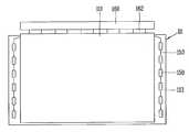
도 3a 및 도 3b는 각각 LED패키지(150)가 부착된 액정패널(110)의 정면도 및 배면도이다.3A and 3B are front and rear views of the liquid crystal panel 110 to which the
도 3a 및 도 3b에 도시된 바와 같이, 제1기판(111) 및 제2기판(113)은 서로 다른 크기로 형성된다. 이때, 제2기판(113)의 가로방향 길이가 제1기판(111)의 가로방향 길이 보다 더 길어서 제1기판(111)의 양측면 외부로 제2기판(113)이 연장되어 제1더미영역(D1)이 형성되고 제1기판(111)의 세로방향 길이가 제2기판(113)의 세로방향 길이 보다 길어서 제2기판(113)의 상부측 외부로 제1기판(111)이 연장되어 제2더미영역(D2)이 형성된다.As shown in FIGS. 3A and 3B, the
상기 제1더미영역(D1)에는 복수의 LED패키지(150)가 일렬로 배치되며, 제2더미영역(D2)에는 FPC(Flexible Printed Circuit;162)이 부착된다.A plurality of
도 3a에 도시된 바와 같이, 상기 제1더미영역(D1)에는 길이방향을 따라 도전패턴(153)이 형성되며, 상기 도전패턴(153) 위에 복수의 LED패키지(150)가 실장된다. 상기 도전패턴(153)은 Al이나 Al합금 등과 같이 전도성이 좋은 금속을 스퍼터링법에 의해 적층되어, 그 위에 실장된 LED패키지(150)에 신호를 공급한다. 상기 LED패키지(150)는 전도성 실런트와 같은 전도성 수지물질에 의해 도전패턴(153) 상부에 부착된다.As shown in FIG. 3A, a
도 3b에 도시된 바와 같이, 제2더미영역(D2)에는 FPC(Flexible Printed Circuit board;162)의 일단이 부착된다. 이때, 상기 FPC(162)의 타단에는 인쇄회로기판(160)이 부착된다. 도면에는 도시하지 않았지만, 상기 FPC(162)에는 게이트구동부와 데이터구동부가 실장되어 액정패널(110) 내부에 주사신호 및 화상신호를 인가함으로써 액정패널(110)을 구동한다. 상기 제2더미영역(D2)에는 액정패널(110) 내부에 형성되는 데이터라인에 화상신호를 인가하는 데이터패드 및 데이터연결배선(114)이 형성된다. 또한, 제2더미영역(D2)에는 게이트라인에 주사신호를 인가하는 게이트연결배선이 형성될 수도 있다.As shown in FIG. 3B, one end of an FPC (Flexible Printed Circuit Board) 162 is attached to the second dummy region D2. At this time, the other end of the
인쇄회로기판(160)에는 FPC(162)에 실장된 게이트구동부와 데이터구동부에 동기신호와 같은 제어신호를 출력하여 게이트구동부와 데이터구동부가 주사신호 및 데이터신호를 생성하도록 하는 제어부, DC/DC 전압변환회로, 감마전압회로 등과 같은 각종 구동소자가 실장된다.The printed
또한, 상기 인쇄회로기판(160)에는 상기 제1더미영역(D1)에 형성되는 도전패턴(153)에 전압을 공급하는 전압공급부가 실장될 수 있다. 이때, 도면에는 도시하지 않았지만, 상기 제1기판(111)과 제2기판(113) 사이에는 은도트(Ag dot)가 배치되어 제2기판(113)에 형성된 도전패턴(153)과 제1기판(111)에 형성되는 전압인가패턴(도면에 표시하지 않음) 사이를 전기적으로 도통하여 상기 도전패턴(153)에 전압을 공급함으로써 상기 LED패키지(150)를 구동한다.In addition, a voltage supply unit for supplying a voltage to the
상기 제1더미영역(D1)과 제2더미영역(D2)은 동일한 기판에 형성되어 LED패키지(150)와 FPC(162)가 동일한 기판에 실장되고 부착될 수 있다.The first dummy region D1 and the second dummy region D2 may be formed on the same substrate so that the
즉, 도 4에 도시된 바와 같이, 제2기판(113)의 면적이 제1기판(111)의 면적보다 작게 형성되어 제1기판(111)의 좌우 및 상부 측면이 외부로 노출되어, 좌우측의 제1더미영역(D1)에는 도전패턴(153)이 형성되어 복수의 LED패키지(150)가 상기 도전패턴(153) 위에 실장되고 제2더미영역(D1)에는 FPC(162)가 부착된다.That is, as shown in FIG. 4, the area of the
이때, 상기 제2더미영역(D2)에는 LED전압 공급용 연결배선(165)이 형성되어, 상기 인쇄회로기판(160)에 실장되는 전원공급부(도면표시하지 않음)의 전압이 FPC(162) 및 상기 LED전압 공급용 연결배선(165)을 통해 상기 도전패턴(153)으로 공급된 후 LED패키지(150)에 인가되어 LED패키지(150)가 구동하게 된다.In this case, a
종래 액정표시소자에서는 박막트랜지스터가 형성되는 제1기판, 즉 박막트랜지스터 어레이기판이 액정패널의 하부에 형성되어 도광판을 출력하는 광이 제1기판으로 입사된 후 제2기판을 통해 출력되는데 반해, 이 구조의 액정표시소자에서는 제1기판(111), 즉 박막트랜지스터 어레이기판이 액정패널(110)의 상부에 형성되고 제2기판(113), 즉 컬러필터기판이 액정패널(110)의 하부에 배치된다.In the conventional liquid crystal display device, a first substrate on which a thin film transistor is formed, that is, a thin film transistor array substrate is formed under the liquid crystal panel so that light for outputting the light guide plate is incident on the first substrate and then output through the second substrate. In a liquid crystal display device having a structure, a
상기 도전패턴(153) 위에 실장되는 LED패키지(150)는 백색광을 발광하는 백색광 LED패키지이다. 물론 본 발명에서 단색광을 발광하는 LED패키지(150)를 설치할 수도 있지만, 이 경우 액정패널(110)에 백색광을 공급하기 위해서는 R,G,B LED패키지(150)를 구비해야만 하기 때문에, 실장되는 LED패키지(150)의 갯수가 증가하고 이들 R,G,B LED패키지(150)를 혼합하여 액정패널(110)에 균일한 백색광을 공급하는데 문제가 있었다.The
따라서, 본 발명에서는 백색광 LED패키지(150)를 제1더미영역(D1)에 실장하여 액정패널(110)에 백색광을 공급하는데, 이러한 백색광 LED패키지(150)가 도 5에 도시되어 있다.Accordingly, in the present invention, the white
도 5에 도시된 바와 같이, LED패키지(150)는 기판(155) 상에 형성되는 LED소자(154)와 상기 LED소자(154)를 수용하는 몰드프레임(158)을 포함하여 구성된다. 그리고, 상기 LED소자(154)의 상부와 대응하는 몰드프레임(158) 내부에는 LED소자(154)를 보호하는 실리콘에폭시 등이 충진되어 보호층(159)이 형성된다. 이때, 상기 기판(155)은 PCB(printed circuit boad)가 사용될 수 있다. 또한, 도면에는 도시하지 않았지만, 상기 몰드프레임(158) 내부 또는 외부 표면에는 정전기방지막이 형성되어 LED소자(154) 내부에 정전기가 발생하는 것을 방지할 수 있게 된다.As shown in FIG. 5, the
도면에는 자세히 도시하지 않았지만, 상기 LED소자(154)는 반도체기판 상에 N형 불순물이 주입된 반도체층과 P형 불순물이 주입된 반도체층으로 이루어진 제1반도체층과 상기 제1반도체층의 N형 반도체응과 P형 반도체층에 각각 형성된 패드로 구성되며, 상기 패드는 와이어(156)에 의해 기판(155)과 전기적으로 연결되어 신호가 인가되며, 상기 LED소자(154)는 형광층(157)에 의해 둘러 싸이게 된다.Although not shown in detail in the drawing, the
상기 형광층(157)은 LED소자(154)가 발광하는 광과는 다른 컬러의 형광물질로서, LED소자(154)로부터 입사되는 광이 일부 흡수되어 다른 컬러의 광이 발광되어, 결국 혼합된 광(즉, 백색광)이 출력된다. 예를 들어, LED소자(154)가 적색광을 발광하는 소자인 경우, 형광층(157)은 녹색 형광물질과 청색 형광물질이 혼합된 층으로 형성하여 상기 LED소자(154)로부터 적색광이 입사됨에 따라 형광층(157)에서는 청녹색(cyan)의 광이 방출하게 된다. 이 청녹색의 광은 상기 LED소자(154)에서 발광되는 적색의 광과 혼합되어 결국 LED패키지(150)로부터는 백색광이 출력된다.The
또한, LED소자(154)를 녹색광을 출력하는 소자로 설치하고 형광층(157)을 적색 형광물질과 청색 형광물질이 혼합된 층으로 형성하여, 녹색광이 형광층(157)으로 입사됨에 따라 형광층(157)으로부터 다홍색(magenta)의 광이 방출하게 되며, 결국 이 다홍색의 광이 상기 녹색 LED소자(154)에서 발광되는 녹색의 광과 혼합되어 백색광이 되어 상기 LED패키지(150)로부터는 백색광이 출력된다.In addition, the
그리고, LED소자(154)를 청색광을 출력하는 소자로 설치하고 형광층(157)을 적색 형광물질과 녹색 형광물질이 혼합된 층으로 형성하여, 청색광이 형광층(157)으로 입사됨에 따라 형광층(157)으로부터 노란색(yellow)의 광이 방출하게 되며, 결국 이 노란색의 광이 상기 청색 LED소자(154)에서 발광되는 청색의 광과 혼합되어 백색광이 되어 상기 LED패키지(150)로부터는 백색광이 출력된다.In addition, the
한편, 본 발명에서는 LED패키지(150)에 2개의 LED소자(154)를 실장할 수 있다. 이 경우, 형광층(157)은 단일 형광물질로 이루어져 2개의 LED소자(154)로부터 출력되는 광에 의해 광을 출력하며, 2개의 LED소자(154)로부터 출력된 광 및 형광층(157)으로부터 출력된 광이 혼합되어 백색광이 액정패널(110)에 공급되는 것이다.Meanwhile, in the present invention, two
LED기판(155)은 제1더미영역(D1)의 도전패턴(153)위에 부착된다. 이때, LED기판(155)의 하면에는 금속배선이 형성되고 이 금속배선은 관통홀을 통해 LED기판(155)의 상면의 금속배선과 전기적으로 연결되며, 상면의 금속배선은 와이어(156)에 의해 LED소자(154)의 패드와 전기적으로 연결된다. 상기 LED기판(155)은 전도성 실런트와 같은 전도성 접착물질에 의해 도전패턴(153)에 부착되므로, 상기 도전패턴(153)으로 인가되는 신호가 금속배선을 통해 LED소자(154)에 공급된다.The
도전패턴(153)은 전도성이 좋은 금속에 의해 형성되는데, 다양한 방법에 의해 형성될 수 있다. 그러나, 상기 도전패턴(153)은 전도성 페이스트를 제1더미영역(D1)에 도포하여 형성할 수도 있지만, 금속 등을 스퍼터링법 등에 의해 적층함으로써 형성하는 것이 바람직하다. 다시 말해서, 일반적인 액정표시소자의 금속배선 형성방법을 통해 형성할 수 있다. 따라서, 본 발명에서는 도전패턴(153)을 형성하기 위한 별도의 공정이나 공정라인이 필요없이 일반적으로 액정표시소자를 제작하는 공정에 의해 형성되므로, 별도의 비용이 추가되지 않게 된다.The
종래 LED가 도광판의 측면과 마주하도록 배치되어 도광판의 측면을 통해 광이 입사되는데 반해, 상기와 같은 구성의 액정표시소자에서는 도 2에 도시된 바와 같이 LED패키지(150)가 제2기판(113)에 부착되므로 LED패키지(150)가 도광판(120)의 상부에 배치된다. 따라서, LED패키지(150)로부터 발광된 광이 도광판(120)의 측면이 아니라 상면을 통해 입사된 후, 도광판(120)을 따라 가이드되어 도광판(120)의 일단에서 타단으로 가이드되면서 액정패널(110)로 광이 공급된다.Conventionally, the LED is disposed to face the side of the light guide plate so that light is incident through the side of the light guide plate. In the liquid crystal display device having the above-described configuration, as shown in FIG. 2, the
이때, LED패키지(150)로부터 발광된 광중 메인지지부(125)측으로 입사되는 광은 메인지지부(125)의 측면벽을 따라 상부로 연장되는 반사판(127)에 의해 반사되어 다시 도광판(120)의 상면으로 입사된 후, 도광판(120)의 일측에서 타측으로 인도된 후 액정패널(110)로 공급된다.At this time, the light incident from the
상술한 바와 같이, 본 발명에서는 LED패키지(150)가 도광판(120)의 측면이 아니라 상면의 액정패널(110)에 부착되므로, 액정표시소자의 크기를 최소화할 수 있게 되며, 특히 액정표시소자의 베젤의 크기를 최소화할 수 있게 된다.As described above, in the present invention, since the
한편, 상술한 설명에서는 본 발명의 액정표시소자가 특정 구조로 이루어져 있지만, 본 발명이 이러한 특정 구조로만 이루어진 것은 아니다. 예를 들면, LED패키지(150)는 컬러필터가 형성되는 컬러필터기판에만 부착되는 것이 아니라 박막트랜지스터가 형성되는 박막트랜지스터 어레이기판에도 부착될 수 있다.On the other hand, in the above description, the liquid crystal display device of the present invention has a specific structure, but the present invention is not limited to this specific structure. For example, the
또한, 상술한 설명에서는 특정한 구조의 LED패키지가 개시되어 있지만, 본 발명에서는 특정 구조의 LED패키지만 사용하는 것이 아니라 다양한 구조의 LED패키지를 사용할 수 있을 것이다. 그리고, 상술한 설명에서는 메인지지부, 하부구조, 및 상부구조가 특정 구조로 이루어져 있지만, 본 발명이 이러한 특정 구조에 한정되는 것은 아니다. 본 발명은 LED패키지가 액정패널에 부착되어 도광판을 통해 다시 액정패널로 광을 공급할 수만 있다며, 그 이외의 구성은 현재 알려진 어떠한 액정표시소자의 구조에도 적용될 수 있을 것이다.In addition, although the LED package having a specific structure is disclosed in the above description, the present invention may use LED packages having various structures instead of using only the LED package having a specific structure. In addition, in the above description, the main support, the lower structure, and the upper structure are made of a specific structure, but the present invention is not limited to this specific structure. According to the present invention, the LED package is attached to the liquid crystal panel and can only supply light back to the liquid crystal panel through the light guide plate, but other configurations may be applied to the structure of any liquid crystal display device currently known.
따라서, 본 발명의 다른 예나 변형예는 본 발명의 기본적인 개념을 이용한 액정표시소자는 본 발명이 속하는 기술분야에 종사하는 사람이라면 누구나 용이하게 창안할 수 있을 것이다.Accordingly, other examples or modifications of the present invention can be easily created by anyone who is engaged in the technical field to which the present invention belongs, using the basic concept of the present invention.
110 : 액정패널111,113 : 기판
120 : 도광판125 : 메인지지부
127 : 반사판130 : 광학시트
140 : 하부커버142 : 상부커버
150 : LED패키지153 : 도전패턴
154 : LED소자110: liquid crystal panel 111,113: substrate
120: light guide plate 125: main support portion
127: reflector 130: optical sheet
140: lower cover 142: upper cover
150: LED package 153: conductive pattern
154: LED device
Claims (11)
Translated fromKorean상기 액정패널 하부에 배치된 도광판;
상기 도광판 상부의 액정패널에 부착되어 도광판의 상면을 통해 광을 입사시켜 액정패널에 광을 공급하는 복수의 LED패키지로 구성된 액정표시소자.A liquid crystal panel;
A light guide plate disposed under the liquid crystal panel;
And a plurality of LED packages attached to the liquid crystal panel on the light guide plate to supply light to the liquid crystal panel by injecting light through the upper surface of the light guide plate.
제1기판 및 제2기판;
상기 제1기판에 형성되어 복수의 화소영역을 정의하는 복수의 게이트라인 및 데이터라인;
상기 화소영역 각각에 형성된 박막트랜지스터; 및
제2기판에 형성된 컬러필터층으로 이루어진 것을 특징으로 하는 액정표시소자.The liquid crystal display device according to claim 1,
A first substrate and a second substrate;
A plurality of gate lines and data lines formed on the first substrate to define a plurality of pixel regions;
A thin film transistor formed in each of the pixel regions; And
And a color filter layer formed on the second substrate.
상기 액정패널이 놓이는 메인지지부;
상기 액정패널과 도광판 사이에 배치되어 도광판을 출력하는 광의 효율을 향상시키는 광학시트;
상기 도광판 하부에 배치된 반사판; 및
상기 액정패널 및 도광판을 조립하는 하부커버 및 상부커버를 추가로 포함하는 것을 특징으로 하는 액정표시소자.The method of claim 1,
A main support portion on which the liquid crystal panel is placed;
An optical sheet disposed between the liquid crystal panel and the light guide plate to improve the efficiency of light outputting the light guide plate;
A reflector disposed under the light guide plate; And
And a lower cover and an upper cover for assembling the liquid crystal panel and the light guide plate.
Priority Applications (1)
| Application Number | Priority Date | Filing Date | Title |
|---|---|---|---|
| KR1020110087422AKR20130024163A (en) | 2011-08-30 | 2011-08-30 | Liquid crystal display device including substrate having emitting device attached thereon |
Applications Claiming Priority (1)
| Application Number | Priority Date | Filing Date | Title |
|---|---|---|---|
| KR1020110087422AKR20130024163A (en) | 2011-08-30 | 2011-08-30 | Liquid crystal display device including substrate having emitting device attached thereon |
Publications (1)
| Publication Number | Publication Date |
|---|---|
| KR20130024163Atrue KR20130024163A (en) | 2013-03-08 |
Family
ID=48176280
Family Applications (1)
| Application Number | Title | Priority Date | Filing Date |
|---|---|---|---|
| KR1020110087422AWithdrawnKR20130024163A (en) | 2011-08-30 | 2011-08-30 | Liquid crystal display device including substrate having emitting device attached thereon |
Country Status (1)
| Country | Link |
|---|---|
| KR (1) | KR20130024163A (en) |
Cited By (4)
| Publication number | Priority date | Publication date | Assignee | Title |
|---|---|---|---|---|
| US9423661B2 (en) | 2013-12-19 | 2016-08-23 | Samsung Display Co., Ltd. | Liquid crystal display |
| US9666147B2 (en) | 2013-12-05 | 2017-05-30 | Samsung Display Co., Ltd. | Data driving apparatus providing data signals to data lines in a display apparatus |
| KR20190080607A (en)* | 2017-12-28 | 2019-07-08 | 엘지디스플레이 주식회사 | Display device |
| KR20190111458A (en) | 2018-03-23 | 2019-10-02 | 유현준 | Resident building |
- 2011
- 2011-08-30KRKR1020110087422Apatent/KR20130024163A/ennot_activeWithdrawn
Cited By (4)
| Publication number | Priority date | Publication date | Assignee | Title |
|---|---|---|---|---|
| US9666147B2 (en) | 2013-12-05 | 2017-05-30 | Samsung Display Co., Ltd. | Data driving apparatus providing data signals to data lines in a display apparatus |
| US9423661B2 (en) | 2013-12-19 | 2016-08-23 | Samsung Display Co., Ltd. | Liquid crystal display |
| KR20190080607A (en)* | 2017-12-28 | 2019-07-08 | 엘지디스플레이 주식회사 | Display device |
| KR20190111458A (en) | 2018-03-23 | 2019-10-02 | 유현준 | Resident building |
Similar Documents
| Publication | Publication Date | Title |
|---|---|---|
| KR102108214B1 (en) | Light emitting diode assembly and liquid crystal display device having the same | |
| CN105652491B (en) | Liquid crystal disply device and its preparation method | |
| KR101299130B1 (en) | Liquid crystal display device | |
| CN103033966B (en) | Liquid crystal indicator module | |
| KR20100109785A (en) | Liquid crystal display device | |
| KR20130027335A (en) | Liquid crystal display devece | |
| KR101295146B1 (en) | Liquid crystal display device | |
| JP2008177170A (en) | Backlight assembly and display device having the same | |
| KR20100078296A (en) | Liquid crystal display device module | |
| KR20120068499A (en) | Backlight unit and liquid crystal display device and method having the same | |
| KR101950831B1 (en) | Liquid crystal display device module | |
| KR101792104B1 (en) | Light guide plate and liquid crystal display device having thereof | |
| KR20090128693A (en) | Liquid crystal display device | |
| KR101796553B1 (en) | Liquid crystal display device | |
| KR20120072958A (en) | Back light and liquid crystal display device having thereof | |
| KR20130024163A (en) | Liquid crystal display device including substrate having emitting device attached thereon | |
| KR20130126407A (en) | Liquid crystal display device | |
| KR101920760B1 (en) | Liquid crystal display module inculding backlight unit | |
| KR20120047715A (en) | Light emitting diode, back light unit and liquid crystal display device having thereof | |
| KR102192957B1 (en) | Back light having light emitting device array | |
| KR20130001522A (en) | Cover bottom and liquid crystal display device module including the same | |
| KR101634632B1 (en) | Connecting structure of light emitting device substrate and flexible pinited circuit board, and liquid crystal display device having thereof | |
| KR102170086B1 (en) | Connector | |
| KR102045448B1 (en) | Liquid crystal display, LCD | |
| KR102057889B1 (en) | Liquid crystal display device having light emitting device back light unit |
Legal Events
| Date | Code | Title | Description |
|---|---|---|---|
| PA0109 | Patent application | Patent event code:PA01091R01D Comment text:Patent Application Patent event date:20110830 | |
| PG1501 | Laying open of application | ||
| PC1203 | Withdrawal of no request for examination | ||
| WITN | Application deemed withdrawn, e.g. because no request for examination was filed or no examination fee was paid |