KR20120136217A - Optical device and method for the same - Google Patents
Optical device and method for the sameDownload PDFInfo
- Publication number
- KR20120136217A KR20120136217AKR1020110055294AKR20110055294AKR20120136217AKR 20120136217 AKR20120136217 AKR 20120136217AKR 1020110055294 AKR1020110055294 AKR 1020110055294AKR 20110055294 AKR20110055294 AKR 20110055294AKR 20120136217 AKR20120136217 AKR 20120136217A
- Authority
- KR
- South Korea
- Prior art keywords
- powder
- optical device
- base material
- reflective surface
- sic
- Prior art date
- Legal status (The legal status is an assumption and is not a legal conclusion. Google has not performed a legal analysis and makes no representation as to the accuracy of the status listed.)
- Withdrawn
Links
- 230000003287optical effectEffects0.000titleclaimsabstractdescription29
- 238000000034methodMethods0.000titleclaimsdescription22
- 239000000843powderSubstances0.000claimsabstractdescription37
- HBMJWWWQQXIZIP-UHFFFAOYSA-Nsilicon carbideChemical compound[Si+]#[C-]HBMJWWWQQXIZIP-UHFFFAOYSA-N0.000claimsabstractdescription37
- 239000000463materialSubstances0.000claimsabstractdescription32
- 238000004519manufacturing processMethods0.000claimsabstractdescription16
- 238000005245sinteringMethods0.000claimsabstractdescription5
- 238000005498polishingMethods0.000claimsabstractdescription3
- OKTJSMMVPCPJKN-UHFFFAOYSA-NCarbonChemical compound[C]OKTJSMMVPCPJKN-UHFFFAOYSA-N0.000claimsdescription12
- 239000002245particleSubstances0.000claimsdescription11
- 229910052799carbonInorganic materials0.000claimsdescription8
- 239000011347resinSubstances0.000claimsdescription8
- 229920005989resinPolymers0.000claimsdescription8
- 238000002156mixingMethods0.000claimsdescription5
- 229910010271silicon carbideInorganic materials0.000description30
- 239000007789gasSubstances0.000description11
- 230000000052comparative effectEffects0.000description9
- 239000011148porous materialSubstances0.000description7
- 239000012535impuritySubstances0.000description6
- 229910002804graphiteInorganic materials0.000description4
- 239000010439graphiteSubstances0.000description4
- 239000012071phaseSubstances0.000description4
- 239000000758substrateSubstances0.000description3
- XUIMIQQOPSSXEZ-UHFFFAOYSA-NSiliconChemical compound[Si]XUIMIQQOPSSXEZ-UHFFFAOYSA-N0.000description2
- 230000002411adverseEffects0.000description2
- 238000005260corrosionMethods0.000description2
- 230000007797corrosionEffects0.000description2
- 239000013078crystalSubstances0.000description2
- 229910003460diamondInorganic materials0.000description2
- 239000010432diamondSubstances0.000description2
- 230000000694effectsEffects0.000description2
- 239000007791liquid phaseSubstances0.000description2
- 239000000203mixtureSubstances0.000description2
- 238000012986modificationMethods0.000description2
- 230000004048modificationEffects0.000description2
- 229920000642polymerPolymers0.000description2
- 238000000197pyrolysisMethods0.000description2
- 229910052710siliconInorganic materials0.000description2
- 239000010703siliconSubstances0.000description2
- 238000000815Acheson methodMethods0.000description1
- 239000004372Polyvinyl alcoholSubstances0.000description1
- 229910004298SiO 2Inorganic materials0.000description1
- 238000005299abrasionMethods0.000description1
- 239000003082abrasive agentSubstances0.000description1
- 239000000654additiveSubstances0.000description1
- 230000000996additive effectEffects0.000description1
- 238000009767auto-combustion synthesis reactionMethods0.000description1
- 239000006229carbon blackSubstances0.000description1
- 238000003763carbonizationMethods0.000description1
- 239000000919ceramicSubstances0.000description1
- 229910010293ceramic materialInorganic materials0.000description1
- 239000002131composite materialSubstances0.000description1
- 238000000280densificationMethods0.000description1
- 238000010304firingMethods0.000description1
- 230000005484gravityEffects0.000description1
- 238000010438heat treatmentMethods0.000description1
- 239000011261inert gasSubstances0.000description1
- 239000003562lightweight materialSubstances0.000description1
- 239000004973liquid crystal related substanceSubstances0.000description1
- 238000000465mouldingMethods0.000description1
- 230000003647oxidationEffects0.000description1
- 238000007254oxidation reactionMethods0.000description1
- 239000005011phenolic resinSubstances0.000description1
- 229920000058polyacrylatePolymers0.000description1
- 229920002451polyvinyl alcoholPolymers0.000description1
- 239000002994raw materialSubstances0.000description1
- 239000004065semiconductorSubstances0.000description1
- 239000007787solidSubstances0.000description1
- 238000009628steelmakingMethods0.000description1
Images


Classifications
- B—PERFORMING OPERATIONS; TRANSPORTING
- B24—GRINDING; POLISHING
- B24B—MACHINES, DEVICES, OR PROCESSES FOR GRINDING OR POLISHING; DRESSING OR CONDITIONING OF ABRADING SURFACES; FEEDING OF GRINDING, POLISHING, OR LAPPING AGENTS
- B24B13/00—Machines or devices designed for grinding or polishing optical surfaces on lenses or surfaces of similar shape on other work; Accessories therefor
- C—CHEMISTRY; METALLURGY
- C04—CEMENTS; CONCRETE; ARTIFICIAL STONE; CERAMICS; REFRACTORIES
- C04B—LIME, MAGNESIA; SLAG; CEMENTS; COMPOSITIONS THEREOF, e.g. MORTARS, CONCRETE OR LIKE BUILDING MATERIALS; ARTIFICIAL STONE; CERAMICS; REFRACTORIES; TREATMENT OF NATURAL STONE
- C04B35/00—Shaped ceramic products characterised by their composition; Ceramics compositions; Processing powders of inorganic compounds preparatory to the manufacturing of ceramic products
- C04B35/515—Shaped ceramic products characterised by their composition; Ceramics compositions; Processing powders of inorganic compounds preparatory to the manufacturing of ceramic products based on non-oxide ceramics
- C04B35/56—Shaped ceramic products characterised by their composition; Ceramics compositions; Processing powders of inorganic compounds preparatory to the manufacturing of ceramic products based on non-oxide ceramics based on carbides or oxycarbides
- C04B35/565—Shaped ceramic products characterised by their composition; Ceramics compositions; Processing powders of inorganic compounds preparatory to the manufacturing of ceramic products based on non-oxide ceramics based on carbides or oxycarbides based on silicon carbide
- C—CHEMISTRY; METALLURGY
- C30—CRYSTAL GROWTH
- C30B—SINGLE-CRYSTAL GROWTH; UNIDIRECTIONAL SOLIDIFICATION OF EUTECTIC MATERIAL OR UNIDIRECTIONAL DEMIXING OF EUTECTOID MATERIAL; REFINING BY ZONE-MELTING OF MATERIAL; PRODUCTION OF A HOMOGENEOUS POLYCRYSTALLINE MATERIAL WITH DEFINED STRUCTURE; SINGLE CRYSTALS OR HOMOGENEOUS POLYCRYSTALLINE MATERIAL WITH DEFINED STRUCTURE; AFTER-TREATMENT OF SINGLE CRYSTALS OR A HOMOGENEOUS POLYCRYSTALLINE MATERIAL WITH DEFINED STRUCTURE; APPARATUS THEREFOR
- C30B29/00—Single crystals or homogeneous polycrystalline material with defined structure characterised by the material or by their shape
- C30B29/10—Inorganic compounds or compositions
- C30B29/36—Carbides
- G—PHYSICS
- G02—OPTICS
- G02B—OPTICAL ELEMENTS, SYSTEMS OR APPARATUS
- G02B5/00—Optical elements other than lenses
- G02B5/08—Mirrors
- G02B5/0808—Mirrors having a single reflecting layer
Landscapes
- Chemical & Material Sciences (AREA)
- Engineering & Computer Science (AREA)
- Organic Chemistry (AREA)
- Physics & Mathematics (AREA)
- Materials Engineering (AREA)
- Ceramic Engineering (AREA)
- Crystallography & Structural Chemistry (AREA)
- Manufacturing & Machinery (AREA)
- Metallurgy (AREA)
- Structural Engineering (AREA)
- Inorganic Chemistry (AREA)
- General Physics & Mathematics (AREA)
- Optics & Photonics (AREA)
- Mechanical Engineering (AREA)
- Ceramic Products (AREA)
Abstract
Translated fromKoreanDescription
Translated fromKorean본 기재는 광학 장치 및 이의 제조 방법에 관한 것이다.The present disclosure relates to an optical device and a method of manufacturing the same.
탄화규소(SiC)는 합성재료로서 세라믹스 분야에서 가장 중요한 탄화물이다. 탄화규소는 입방 정(cubic) 결정구조를 갖는 β상과 육방정(hexagonal) 결정구조를 갖는 α상이 존재한다. β상은 1400-1800 ℃의 온도 범위에서 안정하고, α상은 2000℃ 이상에서 형성된다. SiC의 분자량은 40.1 이고, 비중은 3.21이며, 2500℃ 이상에서 분해된다. SiC는 1970년대에 미국 G.E.의 Prochazka에 의해 boron 및 carbon의 첨가로 상압소결이 처음 성공한 이래로 SiC는 고온강도가 높고, 내마모성, 내산화성, 내식성, 크립저항성등의 특성이 우수하여 고온 구조재료로서 주목을 받는 재료이다. 또한, 현재 메카니컬 씰, 베어링, 각종 노즐, 고온 절삭공구, 내화판, 연마재, 제강시 환원재, 피뢰기 등에 광범위하게 사용되고 있는 고급 세라믹 소재이다.Silicon carbide (SiC) is a composite material and is the most important carbide in the field of ceramics. Silicon carbide has a β phase having a cubic crystal structure and an α phase having a hexagonal crystal structure. The β phase is stable in the temperature range of 1400-1800 ° C., and the α phase is formed at 2000 ° C. or higher. The molecular weight of SiC is 40.1, specific gravity is 3.21, and it decomposes at 2500 degreeC or more. SiC has been attracting attention as a high-temperature structural material because of its high temperature strength, abrasion resistance, oxidation resistance, corrosion resistance, creep resistance, etc. It is a material that receives. In addition, it is a high-grade ceramic material widely used in mechanical seals, bearings, various nozzles, high temperature cutting tools, fireproof plates, abrasives, reducing materials in steelmaking, and lightning arresters.
특히, 상기 SiC의 특성으로 인해, 광학용 반사 거울에 적용될 수 있다.In particular, due to the properties of the SiC, it can be applied to optical reflecting mirrors.
실시예는 고품질의 광학 장치를 제공하고자 한다.The embodiment seeks to provide a high quality optical device.
실시예에 따른 광학 장치는, 순도가 99.999% 내지 99.9999999% 로 구성되는 모재; 및 상기 모재의 상면은 입사광을 반사시키는 반사면을 포함한다.Optical device according to the embodiment, the base material consisting of 99.999% to 99.9999999% purity; And the upper surface of the base material includes a reflective surface for reflecting the incident light.
실시예에 따른 광학 장치 제조 방법은, 실리콘카바이드 분말을 준비하는 단계; 상기 분말을 소결하여 소결체를 준비하는 단계; 및 상기 소결체의 어느 한면을 연마하여 반사면을 형성하는 단계를 포함한다.An optical device manufacturing method according to the embodiment comprises the steps of preparing silicon carbide powder; Sintering the powder to prepare a sintered body; And polishing one surface of the sintered body to form a reflective surface.
실시예에 따른 광학 장치는, 모재 및 반사면을 포함하고, 상기 모재의 순도가 99.999% 내지 99.9999999%로써, 초고순도로 구성될 수 있다. 따라서, 불순물에 의해 상기 제조 장치 내 진공도를 저하시키거나 불순물에 의한 악영향을 미치는 것을 줄일 수 있다.The optical device according to the embodiment includes a base material and a reflecting surface, and the purity of the base material is 99.999% to 99.9999999%, and may be configured with ultra high purity. Therefore, it is possible to reduce the degree of vacuum in the manufacturing apparatus due to impurities or to adversely affect the impurities.
상기 반사면은 상기 모재의 상면에 바로 구비될 수 있다. 따라서, 반사면을 위한 별도의 층을 생략할 수 있고, 공정을 단순화할 수 있다. 또한, 비용을 절감할 수 있다. 또한, 상기 반사면이 박리될 위험이 없다.The reflective surface may be directly provided on the upper surface of the base material. Thus, a separate layer for the reflective surface can be omitted and the process can be simplified. In addition, the cost can be reduced. In addition, there is no risk that the reflective surface is peeled off.
상기 반사면은 상기 모재와 동일한 물질을 포함할 수 있다. 상기 반사면 및 상기 모재의 열팽창 계수가 동일하므로, 상기 반사면의 박리나 변형의 우려가 없다. 또한, 상기 반사면의 반사율을 높일 수 있다.The reflective surface may include the same material as the base material. Since the coefficient of thermal expansion of the reflective surface and the base material is the same, there is no fear of peeling or deformation of the reflective surface. In addition, the reflectance of the reflective surface can be increased.
실시예에 따른 광학 장치 제조 방법에서는, 입경이 작은 분말을 사용한다. 상기 분말의 입경이 작기 때문에, 상기 분말을 소결할 경우, 소결체에 포함되는 기공이 매우 적다. 따라서, 상기 기공에 흡착되는 가스의 양을 줄일 수 있다. 이를 통해, 기공에 흡착된 가스가 상기 광학 장치 사용 중에 방출되어, 주위의 진공도를 저하시킬 우려를 줄일 수 있다. 또한, 광학 장치 사용 중에 온도의 불균일로 인해, 광학 장치에 변형이 일어나는 것은 방지할 수 있다. 이로써, 상기 광학 장치의 수명을 늘릴 수 있다.In the optical device manufacturing method according to the embodiment, powder having a small particle size is used. Since the particle diameter of the powder is small, when the powder is sintered, there are very few pores contained in the sintered body. Therefore, the amount of gas adsorbed to the pores can be reduced. Through this, the gas adsorbed in the pores can be released during the use of the optical device, thereby reducing the possibility of lowering the degree of vacuum around. In addition, deformation of the optical device can be prevented due to unevenness of the temperature during use of the optical device. Thereby, the lifetime of the said optical apparatus can be extended.
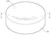
도 1은 실시예에 따른 광학 장치의 사시도이다.
도 2는 도 1의 A-A'를 따라서 절단한 단면을 도시한 단면도이다.
도 3은 실시예에 따른 광학 장치 제조 방법의 공정 흐름도이다.1 is a perspective view of an optical device according to an embodiment.
2 is a cross-sectional view taken along the line A-A 'in Fig.
3 is a process flowchart of the optical device manufacturing method according to the embodiment.
실시예들의 설명에 있어서, 각 층(막), 영역, 패턴 또는 구조물들이 기판, 각 층(막), 영역, 패드 또는 패턴들의 “상/위(on)”에 또는 “하/아래(under)”에 형성된다는 기재는, 직접(directly) 또는 다른 층을 개재하여 형성되는 것을 모두 포함한다. 각 층의 상/위 또는 하/아래에 대한 기준은 도면을 기준으로 설명한다.In the description of embodiments, each layer, region, pattern, or structure may be “on” or “under” the substrate, each layer, region, pad, or pattern. Substrate formed in ”includes all formed directly or through another layer. Criteria for the top / bottom or bottom / bottom of each layer will be described with reference to the drawings.
도면에서 각 층(막), 영역, 패턴 또는 구조물들의 두께나 크기는 설명의 명확성 및 편의를 위하여 변형될 수 있으므로, 실제 크기를 전적으로 반영하는 것은 아니다.The thickness or the size of each layer (film), region, pattern or structure in the drawings may be modified for clarity and convenience of explanation, and thus does not entirely reflect the actual size.
이하, 첨부한 도면을 참조하여 본 발명의 실시예를 상세하게 설명하면 다음과 같다.Hereinafter, embodiments of the present invention will be described in detail with reference to the accompanying drawings.
도 1 및 도 2를 참조하여, 실시예에 따른 광학 장치를 상세하게 설명한다. 도 1은 실시예에 따른 광학 장치의 사시도이다. 도 2는 도 1의 A-A'를 따라서 절단한 단면을 도시한 단면도이다.1 and 2, an optical apparatus according to an embodiment will be described in detail. 1 is a perspective view of an optical device according to an embodiment. FIG. 2 is a cross-sectional view illustrating a cross section taken along line AA ′ of FIG. 1.
도 1 및 도 2를 참조하면, 실시예에 따른 광학 장치는 모재(100) 및 반사면(200)을 포함한다.1 and 2, the optical device according to the embodiment includes a
상기 모재(100)는 순도가 99.999% 내지 99.9999999% 로 구성될 수 있다. 상기 모재(100)는 실리콘카바이드(SiC)를 포함할 수 있다. 즉, 상기 모재(100)는 순도가 99.999% 내지 99.9999999%인 SiC를 포함할 수 있다.The
상기 SiC는 무게가 가벼운 재료이고, 상온에서부터 고온까지 기계적 강도가 높고 안정적인 물질이다. 또한, 열팽창이 적고 열전도도가 좋으며, 내식성이 좋다. 또한, 경도가 높고 내마모성이 우수하다는 장점이 있다. 이러한 SiC를 이용한 광학 반사용 거울이 많이 쓰인다.The SiC is a light weight material, and has a high mechanical strength and stable material from room temperature to high temperature. Moreover, it has little thermal expansion, good thermal conductivity, and good corrosion resistance. In addition, there is an advantage that the hardness is high and the wear resistance is excellent. The mirror for optical reflection using such SiC is used a lot.
반사용 거울은 반도체 제조 장치 또는 액상 제조 장치 등에 사용될 수 있다. 반사용 거울은 방사광, 가시광 또는 X 선을 반사하여 특성을 측정할 수 있도록 가이드할 수 있다.The reflecting mirror can be used in a semiconductor manufacturing apparatus or a liquid crystal manufacturing apparatus. The reflecting mirror may be guided to reflect the emitted light, visible light or X-ray to measure the properties.
상기 반사용 거울은 상기 반사용 거울이 사용되는 제조 장치 내 분위기에 영향을 주지 않고, 그 분위기 내에서 견딜 수 있어야 한다.The reflecting mirror should be able to withstand the atmosphere without affecting the atmosphere in the manufacturing apparatus in which the reflecting mirror is used.
본 실시예에서는, 상기 모재(100)의 순도가 99.999% 내지 99.9999999%로써, 초고순도로 구성될 수 있다. 따라서, 불순물에 의해 상기 제조 장치 내 진공도를 저하시키거나 불순물에 의한 악영향을 미치는 것을 줄일 수 있다.In this embodiment, the purity of the
상기 반사면(200)은 상기 모재(100)의 어느 한 면에 구비된다. 상기 반사면(200)은 상기 모재(100)의 상면에 구비될 수 있다. 본 실시예에서는 상기 반사면(200)이 별도의 층 없이, 상기 모재(100)에 바로 형성될 수 있다. 즉, 상기 반사면(200)은 상기 모재(100)의 상면에 바로 구비될 수 있다. 따라서, 반사면(200)을 위한 별도의 층을 생략할 수 있고, 공정을 단순화할 수 있다. 또한 비용을 절감할 수 있다. 또한, 상기 반사면(200)이 박리될 위험이 없다.The
상기 반사면(200)은 입사광을 반사시킬 수 있다.The
상기 반사면(200)은 상기 모재(100)와 동일한 물질을 포함할 수 있다. 즉, 상기 반사면(200)은 SiC를 포함할 수 있다. 상기 반사면(200) 및 상기 모재(100)의 열팽창 계수가 동일하므로, 상기 반사면(200)의 박리나 변형의 우려가 없다. 또한, 상기 반사면(200)의 반사율을 높일 수 있다.The
종래에는 상기 반사면(200) 및 상기 모재(100)에 포함된 물질이 달라, 열팽창 계수 차이가 존재하였고 이에 따라 반사면(200)이 박리되거나 변형되는 문제가 있었다.Conventionally, the materials included in the
이하, 도 3을 참조하여, 실시예에 따른 광학 장치 제조 방법을 설명한다. 명확하고 간략한 설명을 위해 앞서 설명한 내용과 동일 또는 유사한 부분에 대해서는 상세한 설명을 생략한다.Hereinafter, an optical device manufacturing method according to an embodiment will be described with reference to FIG. 3. For the purpose of clarity and simplicity, detailed description of parts identical or similar to those described above will be omitted.
도 3은 실시예에 따른 광학 장치 제조 방법의 공정 흐름도이다.3 is a process flowchart of the optical device manufacturing method according to the embodiment.
도 3을 참조하면, 실시예에 따른 광학 장치 제조 방법은 분말을 준비하는 단계(ST100), 소결체를 준비하는 단계(ST200) 및 반사면을 형성하는 단계(ST300)를 포함한다.Referring to FIG. 3, the optical device manufacturing method according to the embodiment includes preparing a powder (ST100), preparing a sintered body (ST200), and forming a reflective surface (ST300).
상기 분말을 준비하는 단계(ST100)에서는 SiC 분말을 준비할 수 있다. 특히, 상기 SiC분말의 순도가 99.999% 내지 99.9999999% 일 수 있다.In preparing the powder (ST100), SiC powder may be prepared. In particular, the purity of the SiC powder may be 99.999% to 99.9999999%.
상기 SiC 분말을 얻기 위한 방법으로는, 에치슨(acheson) 공법, 탄소열환원공법(carbo-thermalreduction), 직접 탄화법(directreaction), 액상고분자 열분해법, 고온자전 연소 합성법 등이 있다.As a method for obtaining the SiC powder, there is an Acheson method, a carbon-thermal reduction method, a direct carbonization method, a liquid phase polymer pyrolysis method, and a high temperature auto combustion synthesis method.
상기의 기술들은 SiO2, Si 등의 고상 실리콘 소스와 탄소, 그래파이트 (graphite) 종류의 탄소 소스를 혼합하여 1350℃ 내지 2000℃로 열처리하여 탄화규소를 제조한다.The above-described techniques produce silicon carbide by heat treatment at 1350 ° C. to 2000 ° C. by mixing a solid silicon source such as SiO2 , Si, and a carbon or graphite type carbon source.
특히, 이 중 고순도 탄화규소 분체를 획득하는 방법은 탄소열환원공법 및 액상고분자 열분해법 등이 대표적이다.In particular, the method of obtaining high purity silicon carbide powder is typical of carbon thermal reduction method and liquid phase polymer pyrolysis method.
일례로, 상기 초고순도의 SiC 분말은 다음과 같은 과정을 통해 얻을 수 있다. 먼저, 혼합기에서 SiO 분말과 탄소원을 혼합하여 탄화규소 원료 혼합물을 생성하는 단계를 거칠 수 있다. 여기서 상기 탄소원은 카본 블랙(carbon black)일 수 있다. 또한, 탄소 대 규소의 혼합비는 1.3 이상 1.8 이하일 수 있다.For example, the ultra-high purity SiC powder may be obtained through the following process. First, the step of mixing the SiO powder and the carbon source in the mixer may be a step to produce a silicon carbide raw material mixture. The carbon source may be carbon black. In addition, the mixing ratio of carbon to silicon may be 1.3 or more and 1.8 or less.
이어서, 도가니에서 상기 혼합물을 1300℃ 이상 1400℃ 이하의 온도로 30분 이상 7시간 이하 동안 열처리하여 SiC 분체를 획득하는 단계를 포함한다. 여기서, 상기 도가니의 재료는 흑연이며, 내부 공간에 진공 또는 불활성 가스를 충전할 수 있다.Subsequently, the mixture is heat-treated at a temperature of 1300 ° C. or more and 1400 ° C. or less for 30 minutes or more and 7 hours or less to obtain SiC powder. Here, the material of the crucible is graphite, it can be filled with a vacuum or an inert gas in the interior space.
그러나 실시예가 이에 한정되는 것은 아니고, 상기 초고순도의 SiC 분말을 얻기 위한 다양한 방법이 사용될 수 있다.However, the embodiment is not limited thereto, and various methods for obtaining the ultrapure SiC powder may be used.
이어서, 상기 분말을 준비하는 단계(ST100)에서, 상기 분말의 입경이 0.05 um 내지 3 um 일 수 있다. 상기 분말의 입경이 0.05 um 미만일 경우, 상기 분말을 취급하는데 어려움이 있을 수 있다. 그 결과, 상기 분말을 추후에 소결할 때, 충분한 치밀화를 달성하기 어려울 수 있다. 또한, 성형 및 가공이 어려울 수 있다. 상기 분말의 입경이 3 um 초과할 경우, 핫프레스(hot press)에 의한 소결이 곤란하고, 원하는 기재 강도 및 밀도를 얻기 힘들 수 있다.Subsequently, in the preparing of the powder (ST100), the particle size of the powder may be 0.05 um to 3 um. If the particle diameter of the powder is less than 0.05 um, it may be difficult to handle the powder. As a result, when the powder is subsequently sintered, it may be difficult to achieve sufficient densification. In addition, molding and processing can be difficult. When the particle size of the powder exceeds 3 um, sintering by hot press may be difficult and it may be difficult to obtain a desired substrate strength and density.
상기 분말의 입경이 작기 때문에, 상기 분말을 소결할 경우, 소결체에 포함되는 기공이 매우 적다. 따라서, 상기 기공에 흡착되는 가스의 양을 줄일 수 있다. 이를 통해, 기공에 흡착된 가스가 상기 광학 장치 사용 중에 방출되어, 주위의 진공도를 저하시킬 우려를 줄일 수 있다. 또한, 광학 장치 사용 중에 온도의 불균일로 인해, 광학 장치에 변형이 일어나는 것은 방지할 수 있다. 이로써, 상기 광학 장치의 수명을 늘릴 수 있다.Since the particle diameter of the powder is small, when the powder is sintered, there are very few pores contained in the sintered body. Therefore, the amount of gas adsorbed to the pores can be reduced. Through this, the gas adsorbed in the pores can be released during the use of the optical device, thereby reducing the possibility of lowering the degree of vacuum around. In addition, deformation of the optical device can be prevented due to unevenness of the temperature during use of the optical device. Thereby, the lifetime of the said optical apparatus can be extended.
이어서, 상기 분말을 소결하여 소결체를 준비하는 단계(ST200)를 거친다. 상기 소결체를 준비하는 단계(ST200)는 상기 분말에 수지를 혼합하는 단계를 더 포함할 수 있다. 즉, 상기 분말에 상기 수지를 혼합하여 소결할 수 있다. 여기서, 상기 수지는 탄소를 포함할 수 있다. 일례로, 상기 수지는 페놀수지, 폴리비닐알콜 및 아크릴계 폴리머 등일 수 있다.Subsequently, the powder is sintered to prepare a sintered body (ST200). The preparing of the sintered compact (ST200) may further include mixing a resin with the powder. That is, the resin may be mixed with the powder and sintered. Here, the resin may include carbon. For example, the resin may be a phenol resin, polyvinyl alcohol, an acrylic polymer, or the like.
또한, 상기 소결체를 준비하는 단계(ST200)는 2000 ℃ 내지 2400 ℃ 의 온도에서 이루어질 수 있다.In addition, the step of preparing the sintered body (ST200) may be made at a temperature of 2000 ℃ to 2400 ℃.
구체적으로, 상기 분말에 상기 수지를 혼합하고, 이를 그라파이트 몰드(graphite mold)에 넣는다. 이어서, 약 40 kg/cm3이상의 압력을 가하면서, 2300 ℃의 온도 및 불활성 분위기에서 소성할 수 있다. 이를 통해 소결체를 얻을 수 있다.Specifically, the resin is mixed with the powder, which is placed in a graphite mold. Subsequently, firing may be performed at a temperature of 2300 ° C. and an inert atmosphere while applying a pressure of about 40 kg / cm3 or more. Through this, a sintered compact can be obtained.
이어서, 상기 반사면을 형성하는 단계(ST300)에서는, 상기 소결체의 어느 한면을 연마할 수 있다. 상기 반사면을 형성하는 단계(ST300)에서는 다이아몬드 연마제를 이용할 수 있다.Subsequently, in the forming of the reflective surface (ST300), one surface of the sintered body may be polished. In the forming of the reflective surface (ST300), a diamond abrasive may be used.
본 실시예에서는 별도의 층을 형성하여 상기 반사면을 구비하는 것이 아니므로, 제조 공정을 단순화할 수 있다.In this embodiment, since a separate layer is not provided to provide the reflective surface, the manufacturing process can be simplified.
이하, 실시예를 통하여 본 발명을 좀더 상세하게 설명하고자 한다. 그러나 실시예는 본 발명을 예시하기 위한 것에 불과하며, 본 발명이 이에 한정되는 것은 아니다.Hereinafter, the present invention will be described in more detail with reference to Examples. However, the examples are only for illustrating the present invention, and the present invention is not limited thereto.
실시예Example
순도가 99.9997 % 이상, 입경이 0.7 um 내지 1.5 um 이하의 SiC 미분말에 수지를 혼합하여 그라파이트 몰드에 넣었다. 여기에 40 kg/cm2 이상의 압력을 가하면서 2300 ℃의 온도 및 불활성 분위기 중에서 소성해서 SiC 소결체를 얻었다. 이 소결체의 크기는 직경 60 mm, 높이 10 mm의 원통형이다. 다음으로 다이아몬드 연마제를 이용해서 SiC 소결체의 한 면을 연마 했다.The resin was mixed in a fine SiC powder having a purity of 99.9997% or more and a particle diameter of 0.7 um to 1.5 um or less and placed in a graphite mold. The SiC sintered compact was obtained by baking in 2300 degreeC temperature and inert atmosphere, adding 40 kg / cm <2 > pressure here. The size of this sintered compact is cylindrical of 60 mm in diameter and 10 mm in height. Next, one surface of the SiC sintered body was polished using a diamond abrasive.
비교예1Comparative Example 1
순도 99.8 %, 입경이 1 um의 SiC 분말을 사용하였다는 점을 제외하고는, 실시예와 동일한 방법으로 SiC 소결체를 제작하였다. 이 SiC 소결체의 크기는 40 mm X 150 mm X 300 mm의 육면체이다.A SiC sintered body was produced in the same manner as in Example, except that SiC powder having a purity of 99.8% and a particle size of 1 μm was used. The size of this SiC sintered body is a cube of 40 mm X 150 mm X 300 mm.
비교예2Comparative Example 2
순도 99.2 %, 입경 4 um의 SiC 분말을 사용하고, 소결 조제를 첨가하지 않았다는 점을 제외하고는, 실시예와 동일한 방법으로 SiC 소결체를 제작하였다.A SiC sintered body was produced in the same manner as in Example, except that SiC powder having a purity of 99.2% and a particle size of 4 um was used and no sintering aid was added.
실시예, 비교예1 및 비교예2에 대하여, SiC 함유량, 밀도 및 가스 방출량을 측정하여 표1 에 그 결과를 나타내었다. 여기서, 상기 가스 방출량은 1000 ℃, 10 Torr 내지 5 Torr의 고온, 고진공하에서 측정한 것이다.For Example, Comparative Example 1, and Comparative Example 2, the SiC content, density, and gas emission amount were measured, and the results are shown in Table 1. Here, the gas discharge amount is measured under high temperature and high vacuum of 1000 ℃, 10 Torr to 5 Torr.
표 1을 참조하면, 실시예의 가스 방출량은 100 g 당 0.7 ml로 상당히 적음을 알 수 있다. 비교예1은 SiC 분말의 순도가 낮기 때문에, 상기 실시예에 비해서 SiC 함유량은 적지만 밀도는 더 높게 나왔다. 이것은 비교예1에 포함된 불순물이 첨가제의 역할을 하였기 때문이다. 또한 이러한 소결체중에 존재하는 불순물에 의해 가스 방출량이 많았다. 비교예2에서는 SiC 분말의 입경이 4 um으로 크기 때문에, 상기 실시예에 비해서 SiC 함유량이 적고 밀도가 낮게 나왔다. 이것은 상기 실시예에 비해서 소결체의 기공율이 높은 것을 의미 한다. 이러한 높은 기공율에 기인하여 기공내에 흡착된 가스가 많기 때문에, 가스 방출량이 많았다.Referring to Table 1, it can be seen that the amount of gas released in the examples is considerably less, 0.7 ml per 100 g. In Comparative Example 1, since the purity of the SiC powder was low, the SiC content was lower but the density was higher than that of the above example. This is because an impurity contained in Comparative Example 1 served as an additive. In addition, the amount of gas released was large due to the impurities present in the sintered body. In Comparative Example 2, since the particle size of the SiC powder was large at 4 μm, the SiC content was lower and the density was lower than that of the above Example. This means that the porosity of a sintered compact is high compared with the said Example. Due to such a high porosity, there are many gases adsorbed in the pores, resulting in a large amount of gas discharged.
상술한 실시예에 설명된 특징, 구조, 효과 등은 본 발명의 적어도 하나의 실시예에 포함되며, 반드시 하나의 실시예에만 한정되는 것은 아니다. 나아가, 각 실시예에서 예시된 특징, 구조, 효과 등은 실시예들이 속하는 분야의 통상의 지식을 가지는 자에 의하여 다른 실시예들에 대해서도 조합 또는 변형되어 실시 가능하다. 따라서 이러한 조합과 변형에 관계된 내용들은 본 발명의 범위에 포함되는 것으로 해석되어야 할 것이다.The features, structures, effects and the like described in the foregoing embodiments are included in at least one embodiment of the present invention and are not necessarily limited to one embodiment. In addition, the features, structures, effects, and the like illustrated in the embodiments may be combined or modified with respect to other embodiments by those skilled in the art to which the embodiments belong. Therefore, it should be understood that the present invention is not limited to these combinations and modifications.
또한, 이상에서 실시예들을 중심으로 설명하였으나 이는 단지 예시일 뿐 본 발명을 한정하는 것이 아니며, 본 발명이 속하는 분야의 통상의 지식을 가진 자라면 본 실시예의 본질적인 특성을 벗어나지 않는 범위에서 이상에 예시되지 않은 여러 가지의 변형과 응용이 가능함을 알 수 있을 것이다. 예를 들어, 실시예들에 구체적으로 나타난 각 구성 요소는 변형하여 실시할 수 있는 것이다. 그리고 이러한 변형과 응용에 관계된 차이점들은 첨부한 청구 범위에서 규정하는 본 발명의 범위에 포함되는 것으로 해석되어야 할 것이다.While the present invention has been particularly shown and described with reference to exemplary embodiments thereof, it is clearly understood that the same is by way of illustration and example only and is not to be construed as limiting the scope of the present invention. It can be seen that various modifications and applications are possible. For example, each component specifically shown in the embodiments may be modified. It is to be understood that the present invention may be embodied in many other specific forms without departing from the spirit or essential characteristics thereof.
Claims (8)
Translated fromKorean상기 모재의 상면은 입사광을 반사시키는 반사면을 포함하는 광학 장치.A base material having a purity of 99.999% to 99.9999999%; And
The upper surface of the base material includes a reflecting surface for reflecting incident light.
상기 모재 및 상기 반사면은 실리콘카바이드(SiC)를 포함하는 광학 장치.The method of claim 1,
The base material and the reflecting surface comprises silicon carbide (SiC).
상기 분말을 소결하여 소결체를 준비하는 단계; 및
상기 소결체의 어느 한면을 연마하여 반사면을 형성하는 단계를 포함하는 광학 장치 제조 방법.Preparing silicon carbide powder;
Sintering the powder to prepare a sintered body; And
And polishing a surface of the sintered body to form a reflective surface.
상기 분말을 준비하는 단계에서, 상기 분말의 순도가 99.999% 내지 99.9999999% 인 광학 장치 제조 방법.The method of claim 3,
In the preparing of the powder, the purity of the powder is 99.999% to 99.9999999%.
상기 분말을 준비하는 단계에서, 상기 분말의 입경이 0.05 um 내지 3 um 인 광학 장치 제조 방법.The method of claim 3,
In the preparing of the powder, the particle size of the powder is 0.05 um to 3 um optical device manufacturing method.
상기 소결체를 준비하는 단계는 상기 분말에 수지를 혼합하는 단계를 더 포함하는 광학 장치 제조 방법.The method of claim 3,
Preparing the sintered body further comprises the step of mixing a resin to the powder.
상기 수지는 탄소를 포함하는 광학 장치 제조 방법.The method according to claim 6,
And said resin comprises carbon.
상기 소결체를 준비하는 단계는 2000 ℃ 내지 2400 ℃ 의 온도에서 이루어지는 광학 장치 제조 방법.The method of claim 3,
Preparing the sintered body is an optical device manufacturing method made at a temperature of 2000 ℃ to 2400 ℃.
Priority Applications (1)
| Application Number | Priority Date | Filing Date | Title |
|---|---|---|---|
| KR1020110055294AKR20120136217A (en) | 2011-06-08 | 2011-06-08 | Optical device and method for the same |
Applications Claiming Priority (1)
| Application Number | Priority Date | Filing Date | Title |
|---|---|---|---|
| KR1020110055294AKR20120136217A (en) | 2011-06-08 | 2011-06-08 | Optical device and method for the same |
Publications (1)
| Publication Number | Publication Date |
|---|---|
| KR20120136217Atrue KR20120136217A (en) | 2012-12-18 |
Family
ID=47903738
Family Applications (1)
| Application Number | Title | Priority Date | Filing Date |
|---|---|---|---|
| KR1020110055294AWithdrawnKR20120136217A (en) | 2011-06-08 | 2011-06-08 | Optical device and method for the same |
Country Status (1)
| Country | Link |
|---|---|
| KR (1) | KR20120136217A (en) |
Cited By (6)
| Publication number | Priority date | Publication date | Assignee | Title |
|---|---|---|---|---|
| EP3197845A4 (en)* | 2014-09-25 | 2018-09-12 | Pallidus, Inc. | High purity polysilocarb derived silicon carbide materials, applications and processes |
| US10322936B2 (en) | 2013-05-02 | 2019-06-18 | Pallidus, Inc. | High purity polysilocarb materials, applications and processes |
| US10322974B2 (en) | 2013-05-02 | 2019-06-18 | Pallidus, Inc. | Pressed and self sintered polymer derived SiC materials, applications and devices |
| US10597794B2 (en) | 2013-05-02 | 2020-03-24 | Pallidus, Inc. | High purity polymer derived 3C SiC, methods compositions and applications |
| US11091370B2 (en) | 2013-05-02 | 2021-08-17 | Pallidus, Inc. | Polysilocarb based silicon carbide materials, applications and devices |
| US12330948B2 (en) | 2017-03-29 | 2025-06-17 | Pallidus, Inc. | SiC volumetric shapes and methods of forming boules |
- 2011
- 2011-06-08KRKR1020110055294Apatent/KR20120136217A/ennot_activeWithdrawn
Cited By (7)
| Publication number | Priority date | Publication date | Assignee | Title |
|---|---|---|---|---|
| US10322936B2 (en) | 2013-05-02 | 2019-06-18 | Pallidus, Inc. | High purity polysilocarb materials, applications and processes |
| US10322974B2 (en) | 2013-05-02 | 2019-06-18 | Pallidus, Inc. | Pressed and self sintered polymer derived SiC materials, applications and devices |
| US10597794B2 (en) | 2013-05-02 | 2020-03-24 | Pallidus, Inc. | High purity polymer derived 3C SiC, methods compositions and applications |
| US11091370B2 (en) | 2013-05-02 | 2021-08-17 | Pallidus, Inc. | Polysilocarb based silicon carbide materials, applications and devices |
| US12030819B2 (en) | 2013-05-02 | 2024-07-09 | Pallidus, Inc. | Doped SiC and SiOC compositions and Methods |
| EP3197845A4 (en)* | 2014-09-25 | 2018-09-12 | Pallidus, Inc. | High purity polysilocarb derived silicon carbide materials, applications and processes |
| US12330948B2 (en) | 2017-03-29 | 2025-06-17 | Pallidus, Inc. | SiC volumetric shapes and methods of forming boules |
Similar Documents
| Publication | Publication Date | Title |
|---|---|---|
| KR20120136217A (en) | Optical device and method for the same | |
| KR100276154B1 (en) | Tape cast silicon carbide dummy wafer | |
| TW202009229A (en) | Boroncarbide sintered body and etch apparatus comprising the same | |
| KR101595693B1 (en) | Handle substrate for compound substrate for use with semiconductor | |
| KR102124766B1 (en) | Plasma processing apparatus and manufacturing method of the same | |
| KR101705024B1 (en) | Aln substrate and method for producing same | |
| KR102234171B1 (en) | Manufacturing method of low-resistance silicon carbide composite | |
| KR20070030820A (en) | Nitride sintered body and its manufacturing method | |
| US9676631B2 (en) | Reaction bonded silicon carbide bodies made from high purity carbonaceous preforms | |
| JP2000513689A (en) | New silicon carbide dummy wafer | |
| JP6852463B2 (en) | Fluorescent lens and light emitting device | |
| JP2005166830A (en) | Ceramic heater unit | |
| JP4382919B2 (en) | Method for producing silicon-impregnated silicon carbide ceramic member | |
| KR100970155B1 (en) | Aluminum Nitride Sintered Body | |
| CN112521154A (en) | SiC ceramic device with high-purity working surface and preparation method and application thereof | |
| KR102603574B1 (en) | Pressureless sintered SiC ceramics with 1~30 Ωcm electrical resistivity, its composition, and method for producing the same | |
| JPH06300907A (en) | Optical and X-ray parts using silicon carbide sintered body and method for manufacturing the same | |
| JP5750142B2 (en) | Method for producing modified aluminum nitride sintered body | |
| JP4758617B2 (en) | High-density silicon carbide ceramics and method for producing the same | |
| KR20120135741A (en) | Optical device and method for the same | |
| JP2005039212A (en) | Dummy wafer and manufacturing method therefor | |
| JP4490304B2 (en) | Susceptor | |
| JP2007283435A (en) | Silicon carbide polishing plate, manufacturing method, semiconductor wafer polishing method | |
| KR101142265B1 (en) | High dense silicon carbide for core materials of glass lens and Preparing method thereof | |
| KR102686685B1 (en) | Sintered SiC ceramics with high specific stiffness and composition for producing the same |
Legal Events
| Date | Code | Title | Description |
|---|---|---|---|
| PA0109 | Patent application | Patent event code:PA01091R01D Comment text:Patent Application Patent event date:20110608 | |
| PG1501 | Laying open of application | ||
| PC1203 | Withdrawal of no request for examination | ||
| WITN | Application deemed withdrawn, e.g. because no request for examination was filed or no examination fee was paid |