KR20120122142A - Non-volatile Memory Apparatus and Verification Method Therefor - Google Patents
Non-volatile Memory Apparatus and Verification Method ThereforDownload PDFInfo
- Publication number
- KR20120122142A KR20120122142AKR1020110040148AKR20110040148AKR20120122142AKR 20120122142 AKR20120122142 AKR 20120122142AKR 1020110040148 AKR1020110040148 AKR 1020110040148AKR 20110040148 AKR20110040148 AKR 20110040148AKR 20120122142 AKR20120122142 AKR 20120122142A
- Authority
- KR
- South Korea
- Prior art keywords
- current
- fail
- control signal
- amount
- current control
- Prior art date
- Legal status (The legal status is an assumption and is not a legal conclusion. Google has not performed a legal analysis and makes no representation as to the accuracy of the status listed.)
- Abandoned
Links
Images


Classifications
- G—PHYSICS
- G11—INFORMATION STORAGE
- G11C—STATIC STORES
- G11C16/00—Erasable programmable read-only memories
- G11C16/02—Erasable programmable read-only memories electrically programmable
- G11C16/06—Auxiliary circuits, e.g. for writing into memory
- G11C16/34—Determination of programming status, e.g. threshold voltage, overprogramming or underprogramming, retention
- G11C16/3436—Arrangements for verifying correct programming or erasure
- G11C16/3454—Arrangements for verifying correct programming or for detecting overprogrammed cells
- G11C16/3459—Circuits or methods to verify correct programming of nonvolatile memory cells
- G—PHYSICS
- G11—INFORMATION STORAGE
- G11C—STATIC STORES
- G11C16/00—Erasable programmable read-only memories
- G11C16/02—Erasable programmable read-only memories electrically programmable
- G11C16/06—Auxiliary circuits, e.g. for writing into memory
- G11C16/34—Determination of programming status, e.g. threshold voltage, overprogramming or underprogramming, retention
- G—PHYSICS
- G11—INFORMATION STORAGE
- G11C—STATIC STORES
- G11C16/00—Erasable programmable read-only memories
- G11C16/02—Erasable programmable read-only memories electrically programmable
- G11C16/06—Auxiliary circuits, e.g. for writing into memory
- G—PHYSICS
- G11—INFORMATION STORAGE
- G11C—STATIC STORES
- G11C29/00—Checking stores for correct operation ; Subsequent repair; Testing stores during standby or offline operation
- G11C29/52—Protection of memory contents; Detection of errors in memory contents
- G—PHYSICS
- G11—INFORMATION STORAGE
- G11C—STATIC STORES
- G11C16/00—Erasable programmable read-only memories
- G11C16/02—Erasable programmable read-only memories electrically programmable
- G11C16/04—Erasable programmable read-only memories electrically programmable using variable threshold transistors, e.g. FAMOS
Landscapes
- Read Only Memory (AREA)
- For Increasing The Reliability Of Semiconductor Memories (AREA)
Abstract
Translated fromKoreanDescription
Translated fromKorean본 발명은 반도체 장치에 관한 것으로, 보다 구체적으로는 비휘발성 메모리 장치 및 검증 방법에 관한 것이다.The present invention relates to a semiconductor device, and more particularly to a nonvolatile memory device and a verification method.
비휘발성 메모리 장치, 특히 플래시 메모리 장치는 컴퓨터, 메모리 카드 등에 적용될 뿐 아니라 무선통신 단말기, 디지털 카메라 등과 같은 휴대용 정보 기기로까지 적용 분야가 확대되고 있다.Non-volatile memory devices, in particular flash memory devices are not only applied to computers, memory cards, etc., but are also being applied to portable information devices such as wireless communication terminals and digital cameras.
플래시 메모리 장치에서 각 메모리 셀에 저장된 데이터의 레벨은 메모리 셀의 문턱전압에 의해 정의되고, 따라서 프로그램 동작은 메모리 셀의 문턱전압을 변화시키는 과정이라 말할 수 있다.In the flash memory device, the level of data stored in each memory cell is defined by the threshold voltage of the memory cell. Therefore, the program operation may be referred to as a process of changing the threshold voltage of the memory cell.
도 1은 일반적인 플래시 메모리 장치의 구성도이다.1 is a block diagram of a general flash memory device.
도시한 것과 같이, 플래시 메모리 장치(10)는 메모리 셀 어레이(110), 페이지 버퍼부(120), Y 디코더(130), X 디코더(140), 패일 비트 검출부(150), 전압 공급부(160) 및 전체적인 동작을 제어하는 컨트롤러(170)를 포함한다.As illustrated, the
메모리 셀 어레이(110)는 데이터를 저장하는 복수의 메모리 셀로 구성되며, 각 메모리 셀은 메모리 셀을 선택하여 활성화하는 워드라인(WL)과 메모리 셀의 데이터를 입출력하는 비트라인(BL) 간에 매트릭스 형태로 접속되어 있다. 아울러, 메모리 셀 어레이(110)는 적어도 하나의 칩을 포함할 수 있다.The
페이지 버퍼부(120)는 비트라인(BL)을 통해 메모리 셀 어레이(110)와 접속되는 복수의 페이지 버퍼를 포함하여, 메모리 셀 어레이(110)의 선택된 메모리 셀에 프로그램 데이터를 제공하거나, 메모리 셀 어레이(110)의 선택된 메모리 셀로부터 데이터를 리드하여 저장한다.The
Y 디코더(130)는 컨트롤러(170)의 제어에 따라 페이지 버퍼부(120)의 페이지 버퍼들에 데이터 입출력 경로를 제공하며, X 디코더(140)는 컨트롤러(170)의 제어에 따라 메모리 셀 어레이(110)의 워드라인(WL)을 선택한다.The
전압 공급부(160)는 컨트롤러(170)의 제어에 따라 동작 모드(프로그램, 소거, 리드)에 대응하는 동작 전압을 생성하고, 생성된 동작 전압을 X 디코더(140)를 통해 워드라인(WL) 또는 페이지 버퍼부(120)로 공급한다.The
이러한 플래시 메모리 장치에서 프로그램 동작은 일반적으로 ISPP(Incremental Step Pulse Program) 방식으로 수행된다.Program operation in such a flash memory device is generally performed by an incremental step pulse program (ISPP) method.
만약, 프로그램 대상이 되는 모든 메모리 셀이 동일한 프로그램 속도를 갖는다면 프로그램이 완료된 후 프로그램된 메모리 셀의 문턱전압이 프로그램 전과 동일한 분포를 갖게 될 것이다.If all the memory cells to be programmed have the same program speed, the threshold voltages of the programmed memory cells after the program is completed will have the same distribution as before the program.
하지만 메모리 장치의 제조 공정 중에 발생되는 여러 가지 이유, 메모리 장치의 사용량에 따른 외부 조건의 변화 등에 의해 메모리 셀은 동일한 프로그램 속도를 가질 수 없으므로 프로그램 펄스를 증가시키는 방법으로 즉, ISPP 방식으로 프로그램을 수행하는 것이다.However, since the memory cells cannot have the same program speed due to various reasons that occur during the manufacturing process of the memory device and the change of external conditions according to the usage of the memory device, the program pulse is increased, that is, the program is executed in the ISPP method. It is.
즉, 제 1 단계의 프로그램 펄스를 인가하여 선택된 메모리 셀들에 대한 프로그램을 수행한다. 이후, 선택된 메모리 셀들에 검증전압을 인가하여 문턱전압이 검증전압보다 높은 메모리 셀들을 패스시킨다. 이후, 문턱전압이 검증전압 이하인 메모리 셀들에 대하여 프로그램 전압을 일정한 스텝으로 증가시켜 제 2 단계의 프로그램 펄스를 인가하여 프로그램을 수행한다. 이러한 과정은 모든 셀에 대한 프로그램이 완료될 때까지 수행되며, 이전 프로그램 단계에서 패스된 셀들에 대해서는 프로그램이 금지되도록 하여 오버 프로그램되는 것을 방지한다.That is, the program pulse of the first step is applied to program the selected memory cells. Thereafter, a verification voltage is applied to the selected memory cells to pass the memory cells whose threshold voltage is higher than the verification voltage. Thereafter, the program voltage is increased to the memory cells having the threshold voltage equal to or less than the verify voltage by applying a program pulse of the second step to perform the program. This process is performed until the program for all cells is completed, and the program is prohibited for the cells passed in the previous program step to prevent overprogramming.
이와 같이, 프로그램 동작시 고속 프로그램되는 셀들과 저속 프로그램되는 셀들이 혼재되어 있으므로, 프로그램 동작은 저속 프로그램 셀들이 모두 프로그램 되어야 완료될 수 있다. 따라서, 프로그램 시간은 프로그램 속도가 가장 느린 셀에 의해 결정된다.As described above, since cells to be programmed at high speed and cells to be programmed at low speed are mixed in the program operation, the program operation may be completed when all of the low-speed program cells are programmed. Therefore, the program time is determined by the cell with the slowest program speed.
그런데, 프로그램이 완료되지 않은 셀들 즉, 검증 과정에서 패일 처리된 셀들의 개수가 에러 정정 알고리즘에 의해 복구될 수 있는 수준이라면 굳이 모든 셀이 프로그램될 때까지 프로그램을 수행할 필요가 없을 것이다.However, if the number of cells in which the program is not completed, that is, the number of cells failed to be processed in the verification process is at a level that can be recovered by the error correction algorithm, it may not be necessary to execute the program until all the cells are programmed.
따라서, 패일 비트 검출부(150)를 이용하여 검증 과정에서 패일 처리된 셀의 개수를 카운트한다. 그리고, 컨트롤러(170)의 ECC(Error Correction Circuit)는 패일 비트 검출부(150)의 카운트 결과가 에러 정정 가능한 수준인 경우 해당 셀에 대한 에러 정정을 수행하여 프로그램 동작이 완료되도록 한다.Therefore, the
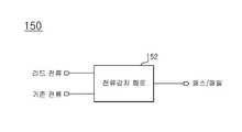
패일 비트 검출부(150)는 일반적으로 전류 감지 회로(Current Sensing Circuit; CSC)를 이용하여 구성되며, 도 2를 참조하여 설명하면 다음과 같다.The fail
도 2는 도 1에 도시한 패일 비트 검출부(150)의 일 예시도이다.FIG. 2 is an exemplary diagram of the
패일 비트 검출부(150)는 메모리 셀 어레이(110)의 선택된 셀들로부터 리드한 전류값과 기준전류를 비교하여 패스/패일 여부를 출력하는 전류 감지 회로(152)를 포함하도록 구성된다. 여기에서, 기준전류는 ECC에 의해 정정 가능한 비트 수에 대응하여 결정된다.The fail
즉, 패일 비트 검출부(150)는 프로그램 후 검증 동작시 프로그램이 미완료된 셀 즉, 패일 비트의 개수만큼 페이지 버퍼의 전류량이 변화하고, 전류량의 변화 정도가 허용 가능한 정도인지의 여부에 따라 패스 또는 패일을 결정하는 것이다.That is, the fail
그런데, 메모리 셀은 그 물리적인 특성에 따라 셀을 통해 흐르는 전류량(셀 전류량)이 편차를 갖는다. 그리고, 이러한 편차의 합이 하나의 셀에 대한 셀 전류량 이상이 되면 패일 비트의 개수를 카운트하는 데 오차가 발생하게 된다. 예를 들어, 모든 셀의 셀 전류량이 의도한 것보다 +10%의 편차를 갖는다면, 10개의 패일 비트를 카운트하고자 하는 경우, 전류량의 편차로 인해 11비트만큼의 전류가 측정될 수 있다.However, in the memory cell, the amount of current flowing through the cell (cell current amount) varies depending on its physical characteristics. When the sum of the deviations is equal to or greater than the cell current amount for one cell, an error occurs in counting the number of fail bits. For example, if the cell current amount of all the cells has a deviation of + 10% than intended, if one wants to count 10 fail bits, current of 11 bits can be measured due to the deviation of the current amount.
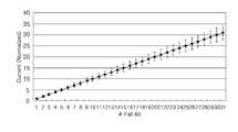
도 3은 패일 비트의 개수에 따른 누적 오차를 설명하기 위한 도면이다.3 is a diagram for describing a cumulative error according to the number of fail bits.
도 3에 도시한 것과 같이, 한 셀에서 흐르는 전류의 크기가 5라고 가정할 때, 패일 비트의 수가 4개 이하로 적을 때에는 셀 전류량의 편차가 패일 비트 검출의 정확도에 영향을 미치지 않는다.As shown in Fig. 3, assuming that the magnitude of the current flowing in one cell is 5, when the number of fail bits is less than four, the variation of the cell current amount does not affect the accuracy of fail bit detection.
하지만, 패일 비트의 개수가 증가할수록 패일 비트 검출부(150)에서 검출되는 총 전류량의 오차는 점차 증가하게 된다.However, as the number of fail bits increases, the error of the total amount of current detected by the
이러한 셀 전류량의 편차는, 패일 비트 검출부(150)의 전류 감지 동작에 영향을 주어 ECC에서 정정 가능한 정도인 것으로 판단되어야 할 경우에도 패일 신호를 출력하거나, ECC에서 정정 가능한 정도가 아닌 경우에도 패스 신호를 출력할 수 있다.The variation of the cell current amount affects the current sensing operation of the fail
본 발명은 셀 전류량의 편차를 감안하여 패일 비트의 개수를 카운트할 수 있는 비휘발성 메모리 장치를 제공하는 데 그 기술적 과제가 있다.SUMMARY OF THE INVENTION The present invention has a technical problem to provide a nonvolatile memory device capable of counting the number of fail bits in consideration of variation in cell current amount.
본 발명의 다른 기술적 과제는 패일 비트의 개수를 정확히 카운트하여 프로그램 성능을 개선할 수 있는 비휘발성 메모리 장치의 검증 방법을 제공하는 데 있다.Another object of the present invention is to provide a method of verifying a nonvolatile memory device that can accurately count the number of fail bits to improve program performance.
상술한 기술적 과제를 달성하기 위한 본 발명의 일 실시예에 의한 비휘발성 메모리 장치는 복수의 워드라인 및 복수의 비트라인 간에 접속되는 복수의 단위 메모리 셀을 포함하는 메모리 셀 어레이; 상기 메모리 셀 어레이의 선택된 메모리 셀로부터 데이터를 리드하여 저장하는 페이지 버퍼부; 검증 명령에 응답하여, 검출하고자 하는 패일 비트의 수 및 리드 동작시 상기 단위 메모리 셀을 통해 흐르는 셀 전류량의 편차에 대응하는 기준전류 생성 신호, 제 1 전류 제어 신호 및 제 2 전류 제어 신호를 생성하는 컨트롤러; 및 상기 검증 명령에 응답하여 상기 컨트롤러로부터 상기 기준전류 생성 신호, 상기 제 1 전류 제어 신호 및 상기 제 2 전류 제어 신호를 제공받아 기준전류량 또는 상기 페이지 버퍼부의 데이터 리드 전류량 중 적어도 하나를 제어하는 패일 비트 검출부;를 포함한다.According to an aspect of the present invention, there is provided a nonvolatile memory device including a memory cell array including a plurality of unit memory cells connected between a plurality of word lines and a plurality of bit lines; A page buffer unit configured to read and store data from selected memory cells of the memory cell array; In response to the verify command, generating a reference current generation signal, a first current control signal, and a second current control signal corresponding to a variation in the number of fail bits to be detected and the amount of cell current flowing through the unit memory cell during a read operation; controller; And a fail bit configured to receive at least one of a reference current generation signal, the first current control signal, and the second current control signal from the controller in response to the verification command to control at least one of a reference current amount and a data read current amount of the page buffer unit. It includes a detection unit.
한편, 본 발명의 다른 실시예에 의한 비휘발성 메모리 장치는 리드 동작시 단위 메모리 셀에 흐르는 셀 전류량이 음(-)의 편차를 갖는 복수의 단위 메모리 셀을 포함하는 메모리 셀 어레이; 및 검증 명령에 응답하여, 기준전류량과 상기 메모리 셀 어레이 중 선택된 메모리 셀에 흐르는 리드 전류량을 비교하되, 검출하고자 하는 패일 비트의 수에 대응하여 상기 기준전류량을 감쇠시켜 상기 리드 전류량과 비교하는 패일 비트 검출부;를 포함한다.On the other hand, the nonvolatile memory device according to another embodiment of the present invention includes a memory cell array including a plurality of unit memory cells having a negative variation in the amount of cell current flowing through the unit memory cells during a read operation; And a fail bit comparing a reference current amount with a read current amount flowing in a selected memory cell of the memory cell array in response to a verification command, and attenuating the reference current amount by comparing the read current amount with the number of fail bits to be detected. It includes a detection unit.
다른 한편, 본 발명의 또 다른 실시예에 의한 비휘발성 메모리 장치는 리드 동작시 단위 메모리 셀에 흐르는 셀 전류량이 양(+)의 편차를 갖는 복수의 단위 메모리 셀을 포함하는 메모리 셀 어레이; 및 검증 명령에 응답하여, 기준전류량과 상기 메모리 셀 어레이 중 선택된 메모리 셀에 흐르는 리드 전류량을 비교하되, 검출하고자 하는 패일 비트의 수에 대응하여 상기 리드 전류량을 감쇠시켜 상기 기준전류량과 비교하는 패일 비트 검출부;를 포함한다.On the other hand, the nonvolatile memory device according to another embodiment of the present invention includes a memory cell array including a plurality of unit memory cells having a positive variation in the amount of cell current flowing through the unit memory cells during a read operation; And a fail bit comparing a reference current amount and a read current amount flowing in a selected memory cell of the memory cell array in response to the verification command, but attenuating the read current amount corresponding to the number of fail bits to be detected to compare with the reference current amount. It includes a detection unit.
한편, 본 발명의 일 실시예에 의한 비휘발성 메모리 장치의 검증 방법은 컨트롤러, 상기 컨트롤러에 의해 제어되는 메모리 셀 어레이 및 패일 비트 검출부를 포함하는 비휘발성 메모리 장치의 검증 방법으로서, 검증 명령에 응답하여, 상기 패일 비트 검출부가 상기 메모리 셀 어레이의 선택된 메모리 셀로부터 데이터 리드 전류를 제공받는 단계; 상기 패일 비트 검출부가 리드 동작시 메모리 셀에 흐르는 셀 전류량의 편차에 대응하여, 검출하고자 하는 패일 비트의 수에 따라 기준전류 또는 상기 리드 전류를 가변시키는 전류 제어 단계; 및 상기 패일 비트 검출부가 상기 기준전류와 상기 리드 전류를 비교하여 패스 패일 여부를 출력하는 단계;를 포함한다.Meanwhile, a verification method of a nonvolatile memory device according to an exemplary embodiment of the present invention is a verification method of a nonvolatile memory device including a controller, a memory cell array controlled by the controller, and a fail bit detection unit. Receiving, by the fail bit detector, a data read current from a selected memory cell of the memory cell array; A current control step of varying the reference current or the read current according to the number of fail bits to be detected, in response to the deviation of the cell current flowing through the memory cell during the read operation by the fail bit detection unit; And outputting, by the fail bit detection unit, whether a pass fails by comparing the reference current with the read current.
본 발명에서는 셀 전류량의 편차를 감안하여 패일 비트 개수를 카운트한다. 메모리 셀은 그 특성에 따라 셀 전류량이 음(-)의 편차를 갖거나 양(+)의 편차를 가질 수 있으므로, 테스트를 통해 편차를 확인하여 둔다. 그리고, 프로그램 검증 동작 중의 패일 비트 수 카운트 시에 리드 전류량을 편차만큼 감소시키거나 기준전류량을 편차만큼 감소시키는 등에 의해 전류량을 보정한다.In the present invention, the number of fail bits is counted in consideration of the variation of the cell current amount. The memory cell may have a negative deviation or a positive deviation depending on its characteristics, so the deviation is confirmed through a test. During the program verify operation, the amount of current is corrected by reducing the amount of read current by the deviation or by reducing the amount of reference current by the deviation.
편차를 고려하지 않고 패일 비트 수를 카운트하는 경우에는 실제 패일 비트 수보다 많거나 적게 카운트될 수 있으나, 본 발명에서와 같이 편차만큼 전류량을 보정하게 되면 패일 비트 수의 카운트 정확도를 향상시킬 수 있다.When counting the number of fail bits without considering the deviation, more or less counts may be made than the actual number of fail bits. However, if the current amount is corrected by the deviation as in the present invention, the count accuracy of the number of fail bits can be improved.
이는 결국, 에러 정정 가능한 패일 비트의 수를 정확히 판단할 수 있는 근거가 되어 프로그램 속도를 단축시킬 수 있는 이점을 제공한다.This, in turn, provides the basis for accurately determining the number of fail correctable fail bits, thus providing the advantage of reducing the program speed.
또한, 카운트하고자 하는 패일 비트의 양에 따라 보정하는 양을 실시간으로 다르게 제어함으로써 패일 비트 검출의 정확도를 항상 유지할 수 있다.In addition, by accurately controlling the amount of correction according to the amount of fail bits to be counted in real time, the accuracy of fail bit detection can always be maintained.
도 1 은 일반적인 비휘발성 메모리 장치의 구성도,
도 2는 도 1에 도시한 패일 비트 검출부의 구성도.
도 3은 패일 비트의 개수에 따른 누적 오차를 설명하기 위한 도면,
도 4는 본 발명의 일 실시예에 의한 비휘발성 메모리 장치의 구성도,
도 5는 도 4에 도시한 전류 제어부의 일 예시도,
도 6은 도 5에 도시한 레지스터에 저장되는 데이터의 일 예시도,
도 7은 도 4에 도시한 오프셋 조절부의 일 예시도,
도 8은 도 4에 도시한 패일 비트 검출부의 일 예시도이다.1 is a configuration diagram of a general nonvolatile memory device;
FIG. 2 is a configuration diagram of the fail bit detection unit shown in FIG. 1. FIG.
3 is a view for explaining a cumulative error according to the number of fail bits;
4 is a configuration diagram of a nonvolatile memory device according to an embodiment of the present invention;
5 is an exemplary diagram of the current control unit shown in FIG. 4;
6 is an exemplary diagram of data stored in a register shown in FIG. 5;
7 is an exemplary view of the offset adjusting unit shown in FIG. 4;
FIG. 8 is an exemplary diagram of a fail bit detector illustrated in FIG. 4.
이하, 첨부된 도면을 참조하여 본 발명의 실시예를 보다 구체적으로 설명한다.Hereinafter, with reference to the accompanying drawings will be described an embodiment of the present invention in more detail.
도 4는 본 발명의 일 실시예에 의한 비휘발성 메모리 장치의 구성도이다.4 is a configuration diagram of a nonvolatile memory device according to an embodiment of the present invention.
도시한 것과 같이, 비휘발성 메모리 장치(20)는 메모리 셀 어레이(210), 페이지 버퍼부(220), Y 디코더(230), X 디코더(240), 패일 비트 검출부(250), 전압 공급부(260) 및 전체적인 동작을 제어하는 컨트롤러(270)를 포함한다.As illustrated, the
메모리 셀 어레이(210)는 데이터를 저장하는 복수의 메모리 셀을 포함하도록 구성된다. 그리고, 각각의 메모리 셀은 워드라인(메모리 셀을 선택하여 활성화)(WL)과 비트라인(메모리 셀의 데이터를 입출력)(BL) 간에 매트릭스 형태로 접속된다. 아울러, 메모리 셀 어레이(210)는 적어도 하나의 칩을 포함하도록 구성할 수 있다.The
페이지 버퍼부(220)는 비트라인(BL)을 통해 메모리 셀 어레이(210)와 접속되는 복수의 페이지 버퍼를 포함하여, 메모리 셀 어레이(210)의 선택된 메모리 셀에 프로그램 데이터를 제공하거나, 메모리 셀 어레이(210)의 선택된 메모리 셀로부터 데이터를 리드하여 저장한다.The
Y 디코더(230)는 컨트롤러(270)의 제어에 따라 페이지 버퍼부(220)의 페이지 버퍼들에 데이터 입출력 경로를 제공하며, X 디코더(240)는 컨트롤러(270)의 제어에 따라 메모리 셀 어레이(210)의 워드라인(WL)을 선택한다.The
전압 공급부(260)는 컨트롤러(270)의 제어에 따라 동작 모드(프로그램, 소거, 리드)에 대응하는 동작 전압을 생성하고, 생성된 동작 전압을 X 디코더(240)를 통해 워드라인(WL) 또는 페이지 버퍼부(220)로 공급한다.The
패일 비트 검출부(250)는 검증 명령에 응답하여 프로그램이 완료되지 않은 셀의 개수 즉, 패일 비트를 카운트한다. 이때, 컨트롤러(270)의 전류 제어부(272)로부터 셀 전류량의 편차에 대응하여 결정되는 전류 제어 신호를 수신하고, 전류 제어 신호에 따라 메모리 셀 어레이(210)의 선택된 셀들로부터 리드한 전류량을 변화시키거나, 또는 기준전류량을 변화시켜, 리드 전류량과 기준전류량을 비교함으로써 패스/패일 여부를 출력한다. 기준전류는 컨트롤러(270)의 ECC에 의해 정정 가능한 비트 수 범위 내에서 결정되며, 특히 패일 비트 검출부(250)에서 검출하고자 하는 셀의 개수는 ECC에 의해 정정 가능한 비트 수 범위 내에서 가변될 수 있다.The fail
보다 구체적으로, 패일 비트 검출부(250)의 비교부(252)는 메모리 셀 어레이(210)의 선택된 셀들로부터 리드한 전류량과 기준전류량을 비교하여 패스/패일 여부를 출력하며, 예를 들어 전류 감지 회로를 이용하여 구성할 수 있다.More specifically, the
오프셋 조절부(254)는 셀 전류량의 편차에 대응하여 결정되는 전류 제어 신호에 따라 리드 전류량 또는 기준전류량을 변화시킨다. 여기에서, 셀 전류량의 편차와, 검출하고자 하는 패일 비트 수에 따른 전류 변화량은 테스트 모드를 통해 미리 측정되거나 결정될 수 있다.The offset adjusting
예를 들어, 셀 전류량의 편차가 양(+)의 편차를 갖는 경우 패일 비트 검출부(250)의 오프셋 조절부(254)는 컨트롤러(270)의 전류 제어부(272)로부터 제 1 전류 제어 신호로서 마이너스 오프셋 신호를 공급받아 기준 전류량을 증가시킨다. 한편, 셀 전류량의 편차가 음(-)의 편차를 갖는 경우 오프셋 조절부(254)는 전류 제어부(272)로부터 제 2 전류 제어 신호로서 플러스 오프셋 신호를 공급받아 리드 전류량을 증가시킨다.For example, when the deviation of the cell current amount has a positive deviation, the offset
본 발명의 다른 실시예에서, 셀 전류량의 편차가 양(+)의 편차를 갖는 경우 플러스 오프셋 신호에 따라 리드 전류량을 감쇠시키고, 셀 전류량의 편차가 음(-)의 편차를 갖는 경우 마이너스 오프셋 신호에 따라 기준 전류량을 증가시키는 것도 가능하다.In another embodiment of the present invention, when the deviation of the cell current amount has a positive deviation, the read current amount is attenuated according to a plus offset signal, and when the deviation of the cell current amount has a negative deviation, a negative offset signal. It is also possible to increase the reference current amount accordingly.
이를 위해, 전류 제어부(272)는 테스트 모드를 통해 측정된 셀 전류량의 편차에 따라, 검출하고자 하는 패일 비트 수에 대응하는 제 1 전류 제어 신호(마이너스 오프셋 전압) 및 제 2 전류 제어 신호(플러스 오프셋 전압)를 저장하고 있으며, 검증 명령이 입력됨에 따라, 제 1 및 제 2 전류 제어 신호를 오프셋 조절부(254)로 제공한다.To this end, the
전류 제어부(272)는 또한 오프셋 조절부(254)로 기준전류 생성 신호를 제공하는데, 기준전류 생성 신호는 검출하고자 하는 패일 비트의 수에 따라 결정된다. 검출하고자 하는 패일 비트의 수에 대응하는 기준전류 생성 신호 또한 전류 제어부(272)에 저장되어 있을 수 있다.The
상술하였듯이, 패일 비트 검출부(250)에서 검출하고자 하는 패일 비트의 개수는 ECC에서 정정 가능한 비트 수 범위 내에서 가변될 수 있으며, 검출하고자 하는 패일 비트의 수는 고정값이거나, 또는 사용자에 의해 결정되는 값일 수 있다.As described above, the number of fail bits to be detected by the fail
한편, 패일 비트 검출부(250)에서 패스 신호가 출력되면 컨트롤러(270)의 ECC는 해당 셀에 대한 에러 정정을 수행하여 프로그램 동작이 완료되도록 한다.Meanwhile, when the pass signal is output from the fail
도 5는 도 4에 도시한 전류 제어부의 일 예시도이다.FIG. 5 is an exemplary diagram of the current control unit shown in FIG. 4.
도 5를 참조하면, 전류 제어부(272)는 레지스터(2721) 및 전류 제어신호 생성부(2723)를 포함하도록 구성된다.Referring to FIG. 5, the
레지스터(2721)는 패일 비트 검출부(250)가 동작하는 데 필요한 제어 신호를 저장한다. 즉, 오프셋 조절부(254)에서 셀 전류량에 따라 전류량을 변화시킬 수 있도록 제 1 전류 제어 신호, 제 2 전류 제어 신호 및 기준전류 생성 신호를 제공한다.The
도 6은 도 5에 도시한 레지스터에 저장되는 데이터의 일 예시도로서, 검출 대상 패일 비트의 수와, 그에 따른 기준전류 생성 신호, 마이너스 오프셋 전압인 제 1 전류 제어 신호 및 플러스 오프셋 전압인 제 2 전류 제어 신호가 저장됨을 알 수 있다.FIG. 6 is an exemplary diagram of data stored in the register shown in FIG. 5, and includes a number of fail target bits, a reference current generation signal, a first current control signal of negative offset voltage, and a second of positive offset voltage. It can be seen that the current control signal is stored.
전류 제어신호 생성부(2723)는 검증 명령에 응답하여, 레지스터(2721)를 참조하여 검출 대상 패일 비트의 수에 대응하는 기준전류 생성 신호(V_refFB), 제 1 전류 제어 신호(V_mOS) 및 제 2 전류 제어 신호(V_pOS)를 오프셋 조절부(254)로 제공한다.In response to the verification command, the current control
본 발명에 의한 전류 제어부(272)는 디코더(2725)를 더 포함할 수 있다. 디코더(2725)는 허용 가능한 패일 비트의 수를 지정된 비트 수로 디코딩하여, 이를 레지스터(2721)에 접근하기 위한 어드레스로 사용할 수 있다.The
예를 들어, 최대 32개의 패일 셀을 검출하고자 하는 경우, 허용 가능한 패일 비트의 수를 5비트의 이진수(00000~11111)로 디코딩할 수 있으며, 디코딩 결과의 상위 3비트를 레지스터(2721)의 어드레스로 지정하는 것이다. 결국, 도 6의 레지스터(2721)에 저장되는 검출 대상 패일 비트의 수는 디코더(2725)의 디코딩한 결과로 저장될 수 있다.For example, if a maximum of 32 fail cells are to be detected, the allowable number of fail bits can be decoded into 5-bit binary numbers (00000 to 11111), and the upper 3 bits of the decoding result are stored in the address of the
도 7은 도 4에 도시한 오프셋 조절부의 일 예시도이다.FIG. 7 is an exemplary view of an offset adjuster illustrated in FIG. 4.
도 7에 도시한 것과 같이, 오프셋 조절부(254)는 기준전류 생성부(2541), 제 1 오프셋 전류 생성부(2543) 및 제 2 오프셋 전류 생성부(2545)를 포함한다.As illustrated in FIG. 7, the offset
기준전류 생성부(2541)는 페이지 버퍼부(220)의 출력단에 인가되는 전류량에 따라 구동되며, 기준전압(VREF) 및 전류 제어부(272)로부터 기준전류 생성 신호(V_refFB)을 인가받아 기준전류를 생성한다.The reference current generator 2551 is driven according to the amount of current applied to the output terminal of the
제 1 오프셋 전류 생성부(2543)는 기준전압(VREF) 및 전류 제어부(272)로부터 제 1 전류 제어 신호(V_mOS)를 공급받아 기준전류량을 변화시킨다.The first offset
제 2 오프셋 전류 생성부(2545)는 기준전압(VREF) 및 전류 제어부(272)로부터 제 2 전류 제어 신호(V_pOS)를 공급받아 페이지 버퍼부(220)의 출력단에 인가되는 리드 전류량을 변화시킨다.The second offset
메모리 셀 어레이(210)에 대한 테스트 결과 각 메모리 셀의 셀 전류량이 음(-)의 편차를 갖는 경우를 가정한다. 프로그램 단계 이후의 검증 과정에서, 패일 비트 검출부(250)의 리드 전류량은 기대치보다 낮게 검출될 것이며, 이는 셀 전류량이 음의 편차를 갖기 때문이다. 따라서, 이러한 경우에는 제 1 전류 제어 신호에 의해 기준전류량을 감쇠시켜 비교부(252)가 패일 비트의 수를 정확히 검출하도록 한다. 본 발명의 다른 실시예에서, 셀 전류량이 음(-)의 편차를 갖는 경우 제 2 전류 제어 신호에 의해 리드 전류량을 증가시키는 것도 가능함은 물론이다.As a result of the test on the
한편, 셀 전류량이 양(+)의 편차를 갖는 경우에는 검증 과정에서 리드 전류량이 기대치보다 높게 검출될 것이다. 따라서, 이 경우에는 제 2 전류 제어 신호에 의해 리드 전류량을 감쇠시키거나, 또는 제 1 전류 제어 신호에 의해 기준 전류량을 증가시켜 비교부(252)가 페일 비트의 수를 정확히 검출할 수 있도록 하게 된다.On the other hand, if the cell current amount has a positive deviation, the read current amount will be detected higher than expected in the verification process. Accordingly, in this case, the read current is attenuated by the second current control signal or the reference current is increased by the first current control signal so that the
도 8은 도 4에 도시한 패일 비트 검출부의 일 예시도이다.FIG. 8 is an exemplary diagram of a fail bit detector illustrated in FIG. 4.
도 8을 참조하면, 패일 비트 검출부(250)는 페이지 버퍼부(도 4의 220)으로부터의 셀 데이터 리드 결과를 제공하는 입력부(256), 입력부(256)에 의한 리드 전류량과 기준전류량을 비교하여 패스/패일 신호(COMP_OUT)를 출력하는 비교부(252) 및 전류 제어부(272)로부터 제공되는 기준전압(VREF), 기준전류 생성 신호(V_refFB), 제 1 전류 제어 신호(V_mOS) 및 제 2 전류 제어 신호(V_pOS)에 응답하여 리드 전류량 또는 기준전류량을 가변시키는 오프셋 조절부(254)를 포함한다.Referring to FIG. 8, the fail
비교부(252)는 전류 감지 회로로 구성할 수 있으나 이에 한정되는 것은 아니다.The
오프셋 조절부(254)는 기준전류 생성부(2541), 제 1 오프셋 전류 생성부(2543) 및 제 2 오프셋 전류 생성부(2545)를 포함하도록 구성된다.The offset
기준전류 생성부(2541)는 전원전압 단자(VDD)에 접속되어 입력부(256)의 출력단에 인가되는 전압에 따라 구동되는 제 1 스위칭 소자(T21), 제 1 스위칭 소자(T21)와 제 1 노드(K1) 간에 접속되어 전원전압(VDD)에 의해 구동되는 제 2 스위칭 소자(T22), 제 1 노드(K1)에 접속되어 기준전압(VREF)에 의해 구동되는 제 3 스위칭 소자(T11) 및 제 3 스위칭 소자(T11)와 접지단자(VSS) 간에 접속되어 기준전류 생성 신호(V_refFB)에 의해 구동되는 제 4 스위칭 소자(T12)를 포함할 수 있다. 제 1 스위칭 소자(T21)는 PMOS 트랜지스터로 구성할 수 있고, 제 2 내지 제 4 스위칭 소자(T11, T12)는 NMOS 트랜지스터로 구성할 수 있으나 이에 한정되는 것은 아니다. 아울러, 제 2 스위칭 소자(T22)는 생략 가능하며, 이 경우 제 1 오프셋 전류 생성부(2543)는 제 1 스위칭 소자(T21)의 드레인단에 접속될 수 있다.The reference current generator 2551 is connected to a power supply voltage terminal VDD and driven according to a voltage applied to an output terminal of the
이와 같이 구성되는 기준전류 생성부(2541)에서, 기준전류 생성 신호(V_refFB)는 검출하고자 하는 패일 비트의 수에 따라 컨트롤러(270)에 의해 결정되며, 기준전압(VREF) 및 기준전류 생성 신호(V_refFB)에 응답하여 제 1 노드(K1)에 기준전류를 인가한다.In the reference current generator 2581 configured as described above, the reference current generation signal V_refFB is determined by the
제 1 오프셋 전류 생성부(2543)는 제 1 노드(K1)에 접속되어 기준전압(VREF)에 의해 구동되는 제 5 스위칭 소자(T23) 및 제 5 스위칭 소자(T23)와 접지 단자(VSS) 간에 접속되어 제 1 전류 제어 신호(V_mOS)에 의해 구동되는 제 6 스위칭 소자(T24)를 포함한다. 여기에서, 제 3 스위칭 소자(T21)는 MPMOS 트랜지스터로, 제 4 내지 제 6 스위칭 소자(T22, T23, T24)는 NMOS 트랜지스터로 구성할 수 있으나 이에 한정되지 않음은 물론이다.The first offset
제 6 스위칭 소자(T24)는 제 1 전류 제어 신호(V_mOS)에 따라 구동되어, 제 1 노드(K1)의 전류량 즉, 기준전류량을 가변시키게 된다.The sixth switching element T24 is driven according to the first current control signal V_mOS to vary the amount of current of the first node K1, that is, the reference current amount.
한편, 제 2 오프셋 전류 생성부(2545)는 입력부(256)의 출력단자에 접속되어 기준전압(VREF)에 의해 구동되는 제 8 스위칭 소자(T32) 및 제 8 스위칭 소자(T32)와 접지단자(VSS) 간에 접속되어 제 2 전류 제어 신호(V_pOS)에 의해 구동되는 제 9 스위칭 소자(T33)를 포함한다. 이에 더하여, 입력부(256)의 출력단자에 인가되는 전류량을 전달하기 위해 전원전압(VDD)에 의해 구동되는 제 7 스위칭 소자(T31)를 더 포함하는 것도 가능하다. 여기에서, 제 7 내지 제 8 스위칭 소자(T31, T32, T33)는 각각 NMOS 트랜지스터로 구성할 수 있으나 이에 한정되지 않는다.Meanwhile, the second offset
제 9 스위칭 소자(T33)는 제 2 전류 제어 신호(V_pOS)에 의해 구동되어, 입력부(256)의 출력단에 인가되는 전류량 즉, 리드 전류량을 가변시킨다.The ninth switching element T33 is driven by the second current control signal V_pOS to vary the amount of current applied to the output terminal of the
메모리 셀의 셀 전류량이 음의 편차를 갖는 경우 리드 전류량은 기대치보다 낮게 측정될 것이다. 이 경우에는 리드 전류량과 비교할 기준전류량을 낮추는 방법으로 편차를 감쇠시킬 수 있으므로, 검출 대상 패일 비트의 수에 대응하여 제 1 전류 제어 신호(V_mOS)를 공급함으로써 제 1 노드(K1)에 인가되는 기준전류량을 낮추어준다. 이 때, 리드 전류량은 변화시키지 않아도 무방하므로 제 2 전류 제어 신호(V_pOS)에 따라 구동되는 제 9 스위칭 소자(T33)는 턴오프 상태를 유지하도록 하는 것이 바람직하다. 다른 방법으로, 리드 전류량을 증가시키는 방법 또한 고려될 수 있으며, 이 경우에는 검출 대상 패일 비트의 수에 대응하여 제 2 전류 제어 신호(V_pOS)를 공급함으로써, 리드 전류량을 증가시킬 수 있다.If the cell current amount of the memory cell has a negative deviation, the read current amount will be measured lower than expected. In this case, since the deviation can be attenuated by lowering the reference current amount to be compared with the read current amount, the reference applied to the first node K1 by supplying the first current control signal V_mOS corresponding to the number of the detected target fail bits. Lower the amount of current. In this case, since the read current amount may not be changed, the ninth switching element T33 driven according to the second current control signal V_pOS is preferably maintained to be turned off. Alternatively, a method of increasing the amount of read current may also be considered. In this case, the amount of read current may be increased by supplying the second current control signal V_pOS corresponding to the number of fail target detection bits.
한편, 메모리 셀의 셀 전류량이 양의 편차를 갖는 경우에는 리드 전류량이 기대치보다 높게 측정되므로, 제 2 전류 제어 신호(V_pOS)에 의해 제 9 스위칭 소자(T33)를 턴온시켜 리드 전류량을 감쇠시킨다. 기준전류량은 변화시키지 않아도 무방하므로, 제 1 전류 제어 신호(V_mOS)에 의해 구동되는 제 6 스위칭 소자(T24)는 턴오프 상태를 갖도록 함이 바람직하다. 다른 방법으로서, 제 1 전류 제어 신호(V_MOS)에 의해 기준전류량을 증가시키는 것도 가능함은 물론이다.On the other hand, when the cell current amount of the memory cell has a positive deviation, since the read current amount is measured to be higher than expected, the ninth switching element T33 is turned on by the second current control signal V_pOS to attenuate the read current amount. Since the reference current amount may not be changed, it is preferable that the sixth switching element T24 driven by the first current control signal V_mOS has a turn-off state. As another method, it is also possible to increase the reference current amount by the first current control signal V_MOS.
이러한 동작을 수행함에 있어서, 기준전류 생성 신호(V_refFB), 제 1 및 제 2 전류 제어 신호(V_mOS, V_pOS)는, 전류 제어부(272)의 디코더(2725)에서 검출 대상 패일 비트의 수를 디코딩한 결과를 어드레스로 하여, 레지스터(2721)로부터 획득한 후, 전류 제어신호 생성부(2723)에서 제공됨은 물론이다.In performing the above operation, the reference current generation signal V_refFB and the first and second current control signals V_mOS and V_pOS are obtained by decoding the number of detected target fail bits in the
본 발명의 용이한 이해를 위해 다음의 경우를 예로 들어 설명한다.For ease of understanding of the present invention, the following case will be described by way of example.
셀 전류량의 편차가 셀 전류량에 대해 +/-(1/N)(N은 자연수)인 메모리 셀 어레이를 가정한다. 이 경우, N개 미만의 셀이 프로그램 미완료된 경우에는 편차가 발생하여도 패일 비트의 개수를 카운트하는 데 영향을 주지 않는다.Assume a memory cell array in which the variation in cell current amount is +/− (1 / N) (N is a natural number) with respect to the cell current amount. In this case, if less than N cells are incompletely programmed, the deviation does not affect counting the number of fail bits.
하지만, MN개(M은 자연수) 이상의 셀이 프로그램 미완료된 경우에는 MN개 단위마다 M개의 셀이 더 카운트되거나 덜 카운트될 수 있다.However, when more than MN cells (M is a natural number) are not fully programmed, M cells may be counted more or less for every MN unit.
따라서, 편차가 +(1/N)인 경우에는 기준전류가 [셀전류*(MN-1)]이 되도록 기준전류 생성 신호를 설정하고, 제 6 스위칭 소자(T24)는 턴오프되도록 제 1 전류 제어 신호(V_mOS)를 로우 레벨로 설정하는 한편, 제 9 스위칭 소자(T33)가 리드 전류량으로부터 [셀 전류*(M-1)]만큼의 전류를 감쇠시킬 수 있도록 제 2 전류 제어 신호(V_pOS)를 설정할 수 있다.Therefore, when the deviation is + (1 / N), the reference current generation signal is set so that the reference current becomes [cell current * (MN-1)], and the first current is set such that the sixth switching element T24 is turned off. While setting the control signal V_mOS to a low level, the second current control signal V_pOS such that the ninth switching element T33 can attenuate a current equal to [cell current * (M-1)] from the read current amount. Can be set.
유사하게, 편차가 -(1/N)인 경우에는 기준전류가 [셀전류*(MN-1)]이 되도록 기준전류 생성 신호를 설정하고, 제 6 스위칭 소자(T24)가 기준전류량으로부터 [셀 전류*(M-1)]만큼의 전류를 감쇠시킬 수 있도록 제 1 전류 제어 신호(V_mOS)를 설정하는 한편, 제 9 스위칭 소자(T33)는 턴오프되도록 제 2 전류 제어 신호(V_pOS)를 로우 레벨로 설정할 수 있다.Similarly, when the deviation is-(1 / N), the reference current generation signal is set such that the reference current is [cell current * (MN-1)], and the sixth switching element T24 is set to [cell] from the reference current amount. Current * (M-1)] to set the first current control signal V_mOS to attenuate the current, while the ninth switching element T33 turns the second current control signal V_pOS low to turn off. Can be set to level.
상기에서는 셀 전류량이 음의 편차를 갖는 경우에는 기준전류량을 감쇠시키고, 양의 편차를 갖는 경우에는 리드 전류량을 감쇠시키는 것에 대해 설명하였으나, 이에 한정되는 것은 아니다. 즉, 셀 전류량의 음의 편차를 갖는 경우 리드 전류량을 상승시키거나, 양의 편차를 갖는 경우 기준전류를 상승시키는 등, 셀 편차만큼 기준전류량과 리드 전류량과의 차이를 보상해 줄 수 있는 방법이라면 어느 것이든 적용 가능하다.In the above description, the reference current amount is attenuated when the cell current amount has a negative deviation, and the read current amount is attenuated when the cell current amount has a negative deviation, but the present invention is not limited thereto. That is, if there is a method that compensates the difference between the reference current amount and the read current amount by the cell deviation, for example, by increasing the read current amount when the cell current amount has a negative deviation or by increasing the reference current when the positive deviation is obtained. Either is applicable.
이와 같이, 본 발명이 속하는 기술분야의 당업자는 본 발명이 그 기술적 사상이나 필수적 특징을 변경하지 않고서 다른 구체적인 형태로 실시될 수 있다는 것을 이해할 수 있을 것이다. 그러므로 이상에서 기술한 실시예들은 모든 면에서 예시적인 것이며 한정적인 것이 아닌 것으로서 이해해야만 한다. 본 발명의 범위는 상기 상세한 설명보다는 후술하는 특허청구범위에 의하여 나타내어지며, 특허청구범위의 의미 및 범위 그리고 그 등가개념으로부터 도출되는 모든 변경 또는 변형된 형태가 본 발명의 범위에 포함되는 것으로 해석되어야 한다.Thus, those skilled in the art will appreciate that the present invention may be embodied in other specific forms without departing from the spirit or essential characteristics thereof. It is therefore to be understood that the embodiments described above are to be considered in all respects only as illustrative and not restrictive. The scope of the present invention is defined by the appended claims rather than the detailed description and all changes or modifications derived from the meaning and scope of the claims and their equivalents are to be construed as being included within the scope of the present invention do.
20 : 비휘발성 메모리 장치
210 : 메모리 셀 어레이
220 : 페이지 버퍼부
230 : Y 디코더
240 : X 디코더
250 : 패일 비트 검출부
252 : 비교부
254 : 오프셋 조절부
260 : 전압 공급부
270 : 컨트롤러
272 : 전류 제어부20: nonvolatile memory device
210: memory cell array
220: page buffer unit
230: Y decoder
240: X decoder
250: fail bit detection unit
252: comparison unit
254: offset adjustment unit
260: voltage supply
270 controller
272: current control unit
Claims (24)
Translated fromKorean상기 메모리 셀 어레이의 선택된 메모리 셀로부터 데이터를 리드하여 저장하는 페이지 버퍼부;
검증 명령에 응답하여, 검출하고자 하는 패일 비트의 수 및 리드 동작시 상기 단위 메모리 셀을 통해 흐르는 셀 전류량의 편차에 대응하는 기준전류 생성 신호, 제 1 전류 제어 신호 및 제 2 전류 제어 신호를 생성하는 컨트롤러; 및
상기 검증 명령에 응답하여 상기 컨트롤러로부터 상기 기준전류 생성 신호, 상기 제 1 전류 제어 신호 및 상기 제 2 전류 제어 신호를 제공받아 기준전류량 또는 상기 페이지 버퍼부의 데이터 리드 전류량 중 적어도 하나를 제어하는 패일 비트 검출부;
를 포함하는 비휘발성 메모리 장치.A memory cell array including a plurality of unit memory cells connected between a plurality of word lines and a plurality of bit lines;
A page buffer unit configured to read and store data from selected memory cells of the memory cell array;
In response to the verify command, generating a reference current generation signal, a first current control signal, and a second current control signal corresponding to a variation in the number of fail bits to be detected and the amount of cell current flowing through the unit memory cell during a read operation; controller; And
A fail bit detector configured to receive at least one of the reference current generation signal, the first current control signal, and the second current control signal from the controller in response to the verification command to control at least one of a reference current amount and a data read current amount of the page buffer unit; ;
Nonvolatile memory device comprising a.
상기 패일 비트 검출부는, 상기 기준전류 생성 신호 및 상기 제 1 전류 제어 신호에 따라 기준전류를 제어하여 패스 또는 패일 여부를 결정하는 비휘발성 메모리 장치.The method of claim 1,
The fail bit detection unit determines whether to pass or fail by controlling a reference current according to the reference current generation signal and the first current control signal.
상기 패일 비트 검출부는, 상기 제 2 전류 제어 신호에 따라 상기 페이지 버퍼부의 데이터 리드 전류량을 제어하여 패스 또는 패일 여부를 결정하는 비휘발성 메모리 장치.The method of claim 2,
The fail bit detection unit determines whether to pass or fail by controlling an amount of data read current of the page buffer unit according to the second current control signal.
상기 컨트롤러는, 상기 셀 전류량의 편차에 따라 검출하고자 하는 패일 비트의 수에 대응하는 상기 기준전류 생성 신호, 상기 제 1 전류 제어 신호 및 상기 제 2 전류 제어 신호를 생성하는 레지스터; 및
상기 기준전류 생성 신호, 상기 제 1 전류 제어 신호 및 상기 제 2 전류 제어 신호를 상기 패일 비트 검출부로 제공하는 전류 제어신호 생성부;
를 포함하는 비휘발성 메모리 장치.The method of claim 1,
The controller may include: a register configured to generate the reference current generation signal, the first current control signal, and the second current control signal corresponding to the number of fail bits to be detected according to the variation of the cell current amount; And
A current control signal generator providing the reference current generation signal, the first current control signal, and the second current control signal to the fail bit detector;
Nonvolatile memory device comprising a.
상기 컨트롤러는, 상기 검출하고자 하는 패일 비트의 수를 지정된 단위의 이진 비트로 디코딩하는 디코더를 더 포함하는 비휘발성 메모리 장치.The method of claim 4, wherein
The controller further includes a decoder to decode the number of fail bits to be detected into binary bits of a specified unit.
상기 컨트롤러는, 패일 비트에 대한 오류를 정정하는 ECC(Error Correction Circuit)를 포함하며,
상기 검출하고자 하는 패일 비트의 수는 상기 ECC에 의해 정정 가능한 범위 내에서 고정 또는 가변되는 비휘발성 메모리 장치.The method of claim 4, wherein
The controller includes an error correction circuit (ECC) for correcting errors for fail bits,
The number of fail bits to be detected is fixed or variable within a range that can be corrected by the ECC.
상기 패일 비트 검출부는, 상기 검증 명령에 응답하여, 상기 리드 전류량과 상기 기준전류량을 비교하여 패스 또는 패일 여부를 결정하는 비교부; 및
상기 기준전류 생성 신호, 상기 제 1 전류 제어 신호 및 상기 제 2 전류 제어 신호에 응답하여, 상기 기준전류량 또는 상기 리드 전류량을 가변시키는 오프셋 조절부;
를 포함하는 비휘발성 메모리 장치.The method of claim 1,
The fail bit detection unit may include: a comparison unit that determines whether to pass or fail by comparing the read current amount with the reference current amount in response to the verification command; And
An offset adjuster configured to vary the reference current amount or the read current amount in response to the reference current generation signal, the first current control signal, and the second current control signal;
Nonvolatile memory device comprising a.
상기 오프셋 조절부는, 상기 컨트롤러로부터 제공되는 상기 기준전류 생성 신호에 응답하여 상기 기준전류를 생성하는 기준전류 생성부;
상기 컨트롤러로부터 제공되는 상기 제 1 전류 제어 신호에 응답하여 상기 기준전류량을 가변시키는 제 1 오프셋 전류 생성부; 및
상기 컨트롤러로부터 제공되는 상기 제 2 전류 제어 신호에 응답하여 상기 리드 전류량을 가변시키는 제 2 오프셋 전류 생성부;
를 포함하는 비휘발성 메모리 장치.The method of claim 7, wherein
The offset controller may include a reference current generator configured to generate the reference current in response to the reference current generation signal provided from the controller;
A first offset current generator configured to vary the reference current amount in response to the first current control signal provided from the controller; And
A second offset current generator configured to vary the read current amount in response to the second current control signal provided from the controller;
Nonvolatile memory device comprising a.
검증 명령에 응답하여, 기준전류량과 상기 메모리 셀 어레이 중 선택된 메모리 셀에 흐르는 리드 전류량을 비교하되, 검출하고자 하는 패일 비트의 수에 대응하여 상기 기준전류량 또는 상기 리드 전류량을 가변시켜, 상기 기준전류량과 상기 리드 전류량을 비교하는 패일 비트 검출부;
를 포함하는 비휘발성 메모리 장치.A memory cell array including a plurality of unit memory cells having a negative variation in a cell current flowing in the unit memory cell during a read operation; And
In response to the verify command, the reference current amount is compared with the read current amount flowing in the selected memory cell of the memory cell array, and the reference current amount or the read current amount is varied in correspondence to the number of fail bits to be detected, A fail bit detector for comparing the read current amount;
Nonvolatile memory device comprising a.
상기 셀 전류량의 편차에 따라, 상기 검출하고자 하는 패일 비트의 수에 대응하는 전류 제어 신호를 상기 패일 비트 검출부로 제공하는 컨트롤러를 더 포함하고,
상기 패일 비트 검출부는 상기 전류 제어 신호에 응답하여 상기 기준전류량을 감쇠시키는 비휘발성 메모리 장치.The method of claim 9,
And a controller configured to provide the fail bit detection unit with a current control signal corresponding to the number of fail bits to be detected, according to the variation of the cell current amount.
And the fail bit detector attenuates the reference current amount in response to the current control signal.
상기 셀 전류량의 편차에 따라, 상기 검출하고자 하는 패일 비트의 수에 대응하는 전류 제어 신호를 상기 패일 비트 검출부로 제공하는 컨트롤러를 더 포함하고,
상기 패일 비트 검출부는 상기 전류 제어 신호에 응답하여 상기 리드 전류량을 증가시키는 비휘발성 메모리 장치.The method of claim 9,
And a controller configured to provide the fail bit detection unit with a current control signal corresponding to the number of fail bits to be detected, according to the variation of the cell current amount.
And the fail bit detector increases the read current amount in response to the current control signal.
상기 컨트롤러는, 패일 비트에 대한 오류를 정정하는 ECC(Error Correction Circuit)를 포함하며,
상기 검출하고자 하는 패일 비트의 수는 상기 ECC에 의해 정정 가능한 범위 내에서 고정 또는 가변되는 비휘발성 메모리 장치.The method according to any one of claims 10 or 11,
The controller includes an error correction circuit (ECC) for correcting errors for fail bits,
The number of fail bits to be detected is fixed or variable within a range that can be corrected by the ECC.
검증 명령에 응답하여, 기준전류량과 상기 메모리 셀 어레이 중 선택된 메모리 셀에 흐르는 리드 전류량을 비교하되, 검출하고자 하는 패일 비트의 수에 대응하여 상기 기준전류량 또는 상기 리드 전류량을 가변시켜, 상기 기준전류량과 상기 리드 전류량을 비교하는 패일 비트 검출부;
를 포함하는 비휘발성 메모리 장치.A memory cell array including a plurality of unit memory cells having a positive variation in the amount of cell current flowing through the unit memory cells during a read operation; And
In response to the verify command, the reference current amount is compared with the read current amount flowing in the selected memory cell of the memory cell array, and the reference current amount or the read current amount is varied in correspondence to the number of fail bits to be detected, A fail bit detector for comparing the read current amount;
Nonvolatile memory device comprising a.
상기 셀 전류량의 편차에 따라, 상기 검출하고자 하는 패일 비트의 수에 대응하는 전류 제어 신호를 상기 패일 비트 검출부로 제공하는 컨트롤러를 더 포함하고,
상기 패일 비트 검출부는 상기 전류 제어 신호에 응답하여 상기 리드 전류량을 감쇠시키는 비휘발성 메모리 장치.The method of claim 13,
And a controller configured to provide the fail bit detection unit with a current control signal corresponding to the number of fail bits to be detected, according to the variation of the cell current amount.
And the fail bit detector attenuates the read current amount in response to the current control signal.
상기 셀 전류량의 편차에 따라, 상기 검출하고자 하는 패일 비트의 수에 대응하는 전류 제어 신호를 상기 패일 비트 검출부로 제공하는 컨트롤러를 더 포함하고,
상기 패일 비트 검출부는 상기 전류 제어 신호에 응답하여 상기 기준전류량을 증가시키는 비휘발성 메모리 장치.The method of claim 13,
And a controller configured to provide the fail bit detection unit with a current control signal corresponding to the number of fail bits to be detected, according to the variation of the cell current amount.
And the fail bit detector increases the reference current amount in response to the current control signal.
상기 컨트롤러는, 패일 비트에 대한 오류를 정정하는 ECC(Error Correction Circuit)를 포함하며,
상기 검출하고자 하는 패일 비트의 수는 상기 ECC에 의해 정정 가능한 범위 내에서 고정 또는 가변되는 비휘발성 메모리 장치.The method according to any one of claims 14 to 15,
The controller includes an error correction circuit (ECC) for correcting errors for fail bits,
The number of fail bits to be detected is fixed or variable within a range that can be corrected by the ECC.
검증 명령에 응답하여, 상기 패일 비트 검출부가 상기 메모리 셀 어레이의 선택된 메모리 셀로부터 데이터 리드 전류를 제공받는 단계;
상기 패일 비트 검출부가 리드 동작시 메모리 셀에 흐르는 셀 전류량의 편차에 대응하여, 검출하고자 하는 패일 비트의 수에 따라 기준전류 또는 상기 리드 전류를 가변시키는 전류 제어 단계; 및
상기 패일 비트 검출부가 상기 기준전류와 상기 리드 전류를 비교하여 패스 패일 여부를 출력하는 단계;
를 포함하는 비휘발성 메모리 장치의 검증 방법.A verification method of a nonvolatile memory device including a controller, a memory cell array controlled by the controller, and a fail bit detector,
In response to the verify command, the fail bit detector receiving a data read current from a selected memory cell of the memory cell array;
A current control step of varying the reference current or the read current according to the number of fail bits to be detected, in response to the deviation of the cell current flowing through the memory cell during the read operation by the fail bit detection unit; And
Outputting, by the fail bit detector, a pass fail by comparing the reference current with the read current;
Verification method of a nonvolatile memory device comprising a.
상기 셀 전류량이 음(-)의 편차를 갖는 경우 상기 전류 제어 단계는 상기 기준전류를 감쇠시키는 단계인 비휘발성 메모리 장치의 검증 방법.The method of claim 17,
And the current control step attenuates the reference current when the cell current amount has a negative deviation.
상기 셀 전류량이 음(-)의 편차를 갖는 경우 상기 전류 제어 단계는 상기 리드 전류를 증가시키는 단계인 비휘발성 메모리 장치의 검증 방법.The method of claim 17,
And the current control step is to increase the read current when the cell current amount has a negative deviation.
상기 셀 전류량이 양(+)의 편차를 갖는 경우 상기 전류에 제어 단계는 상기 리드 전류를 감쇠시키는 단계인 비휘발성 메모리 장치의 검증 방법.The method of claim 17,
And if the cell current amount has a positive deviation, controlling the current to attenuate the read current.
상기 셀 전류량이 양(+)의 편차를 갖는 경우 상기 전류에 제어 단계는 상기 기준 전류를 증가시키는 단계인 비휘발성 메모리 장치의 검증 방법.The method of claim 17,
And if said cell current amount has a positive deviation, controlling said current to increase said reference current.
상기 전류 제어 단계는, 상기 컨트롤러가 상기 셀 전류량의 편차에 대응하여 검출 대상 패일 비트의 수에 따른 전류 제어 신호를 상기 패일 비트 검출부로 제공하는 단계를 더 포함하고,
상기 패일 비트 검출부는 상기 전류 제어 신호에 따라 기준전류 또는 상기 리드 전류를 가변시키는 비휘발성 메모리 장치의 검증 방법.The method of claim 17,
The current control step may further include providing, by the controller, a current control signal according to the number of detected target fail bits to the fail bit detection unit in response to the variation of the cell current amount.
And the fail bit detection unit varies a reference current or the read current according to the current control signal.
상기 패일 비트 검출부로부터 패스 신호가 출력됨에 따라,
상기 컨트롤러가 패일 비트에 대한 오류를 정정하는 단계를 더 포함하는 비휘발성 메모리 장치의 검증 방법.The method of claim 17,
As a pass signal is output from the fail bit detector,
And correcting, by the controller, an error for a fail bit.
상기 컨트롤러는 상기 패일 비트에 대한 오류를 정정하는 ECC(Error Correction Circuit)를 포함하고,
상기 패일 비트 검출부에서 검출하고자 하는 패일 비트의 수는 상기 ECC에 의해 정정 가능한 범위 내에서 고정 또는 가변되는 비휘발성 메모리 장치의 검증 방법.24. The method of claim 23,
The controller includes an error correction circuit (ECC) to correct an error for the fail bit,
The number of fail bits to be detected by the fail bit detection unit is fixed or variable within a range that can be corrected by the ECC.
Priority Applications (3)
| Application Number | Priority Date | Filing Date | Title |
|---|---|---|---|
| KR1020110040148AKR20120122142A (en) | 2011-04-28 | 2011-04-28 | Non-volatile Memory Apparatus and Verification Method Therefor |
| US13/412,892US8743608B2 (en) | 2011-04-28 | 2012-03-06 | Nonvolatile memory apparatus and verification method thereof |
| CN201210070102.1ACN102760493B (en) | 2011-04-28 | 2012-03-16 | Nonvolatile memory devices and verification method thereof |
Applications Claiming Priority (1)
| Application Number | Priority Date | Filing Date | Title |
|---|---|---|---|
| KR1020110040148AKR20120122142A (en) | 2011-04-28 | 2011-04-28 | Non-volatile Memory Apparatus and Verification Method Therefor |
Publications (1)
| Publication Number | Publication Date |
|---|---|
| KR20120122142Atrue KR20120122142A (en) | 2012-11-07 |
Family
ID=47054920
Family Applications (1)
| Application Number | Title | Priority Date | Filing Date |
|---|---|---|---|
| KR1020110040148AAbandonedKR20120122142A (en) | 2011-04-28 | 2011-04-28 | Non-volatile Memory Apparatus and Verification Method Therefor |
Country Status (3)
| Country | Link |
|---|---|
| US (1) | US8743608B2 (en) |
| KR (1) | KR20120122142A (en) |
| CN (1) | CN102760493B (en) |
Families Citing this family (10)
| Publication number | Priority date | Publication date | Assignee | Title |
|---|---|---|---|---|
| CN103839589B (en)* | 2014-03-17 | 2017-01-18 | 上海华虹宏力半导体制造有限公司 | bit failure detection method |
| CN103886906B (en)* | 2014-03-20 | 2017-01-25 | 上海华力微电子有限公司 | Method for reading current of nonvolatile memory and method for obtaining current distribution state |
| CN106558345A (en)* | 2015-09-25 | 2017-04-05 | 北京兆易创新科技股份有限公司 | A kind of bit scan method and system compared based on electric current |
| KR20170065969A (en)* | 2015-12-04 | 2017-06-14 | 에스케이하이닉스 주식회사 | Memory device and operation method for the same |
| CN109147860B (en)* | 2017-06-27 | 2020-11-17 | 华邦电子股份有限公司 | Memory storage device and test method thereof |
| JP2020091930A (en)* | 2018-12-07 | 2020-06-11 | キオクシア株式会社 | Semiconductor storage device |
| JP7520724B2 (en)* | 2019-01-17 | 2024-07-23 | ソニーセミコンダクタソリューションズ株式会社 | Image capture device, image capture system, and failure detection method |
| US10971213B1 (en)* | 2019-09-24 | 2021-04-06 | Macronix International Co., Ltd. | Data sensing device and data sensing method thereof |
| CN112331255B (en)* | 2020-10-21 | 2022-01-25 | 长江存储科技有限责任公司 | Verification statistical circuit and method of 3D NAND memory and 3D NAND memory |
| US12183381B2 (en)* | 2022-04-19 | 2024-12-31 | Ferroelectric Memory Gmbh | Self-adjusting reference current for a memory |
Family Cites Families (7)
| Publication number | Priority date | Publication date | Assignee | Title |
|---|---|---|---|---|
| US6118699A (en)* | 1998-07-14 | 2000-09-12 | Kabushiki Kaisha Toshiba | Semiconductor memory device using MONOS type nonvolatile memory cell |
| US7237074B2 (en)* | 2003-06-13 | 2007-06-26 | Sandisk Corporation | Tracking cells for a memory system |
| KR100630710B1 (en) | 2004-11-04 | 2006-10-02 | 삼성전자주식회사 | Fail bit detection device of a semiconductor memory capable of detecting a plurality of fail bits |
| KR100927783B1 (en)* | 2007-01-23 | 2009-11-20 | 주식회사 하이닉스반도체 | Fail Bit Verification Circuit and Verification Method of Memory Devices |
| KR20100089508A (en) | 2009-02-04 | 2010-08-12 | 주식회사 하이닉스반도체 | Circuit of testing for fail bit and semiconductor memory device with the same |
| KR101653206B1 (en) | 2010-01-19 | 2016-09-02 | 삼성전자주식회사 | program verification circuit and non-volatile memory device having the same |
| KR20120088442A (en)* | 2011-01-31 | 2012-08-08 | 에스케이하이닉스 주식회사 | Non-Volatile Memory System and Flag Data Input/Output Method Therefor |
- 2011
- 2011-04-28KRKR1020110040148Apatent/KR20120122142A/ennot_activeAbandoned
- 2012
- 2012-03-06USUS13/412,892patent/US8743608B2/enactiveActive
- 2012-03-16CNCN201210070102.1Apatent/CN102760493B/enactiveActive
Also Published As
| Publication number | Publication date |
|---|---|
| CN102760493B (en) | 2016-09-28 |
| US20120275222A1 (en) | 2012-11-01 |
| US8743608B2 (en) | 2014-06-03 |
| CN102760493A (en) | 2012-10-31 |
Similar Documents
| Publication | Publication Date | Title |
|---|---|---|
| KR20120122142A (en) | Non-volatile Memory Apparatus and Verification Method Therefor | |
| CN107452421B (en) | Solid state storage device and state prediction method thereof | |
| KR101578511B1 (en) | Method for setting a read voltage | |
| EP2569775B1 (en) | Determining and using soft data in memory devices and systems | |
| US6963505B2 (en) | Method circuit and system for determining a reference voltage | |
| US8238161B2 (en) | Nonvolatile memory device | |
| US8964477B2 (en) | Nonvolatile memory, electronic apparatus, and verification method | |
| US9299459B2 (en) | Method and apparatus of measuring error correction data for memory | |
| US20120069674A1 (en) | Flash memory device and related program verification method | |
| JP2007510253A (en) | Method, circuit and system for non-volatile memory array read error detection | |
| TW201333952A (en) | Mitigating variations arising from simultaneous multi-state sensing | |
| HK1220283A1 (en) | Reading voltage calculation in solid-state storage devices | |
| JP2009020996A (en) | Nonvolatile memory device and reading method | |
| US9490024B1 (en) | Solid state storage device and reading control method thereof | |
| US20240419339A1 (en) | Erase method for non-volatile memory device and non-volatile memory device using the same | |
| US8351263B2 (en) | Method circuit and system for operating an array of non-volatile memory (“NVM”) cells and a corresponding NVM device | |
| KR101212745B1 (en) | Flash Memory Apparatus and Program Verify Method Therefor | |
| KR20100013962A (en) | Programming method of nonvolatile memory device | |
| US20120198290A1 (en) | Non-volatile memory device and programming method thereof | |
| KR101540795B1 (en) | Method for reading data stored in a flash memory according to a threshold voltage distribution and memory controller and system thereof | |
| US20100192039A1 (en) | Memory device and operation method thereof | |
| US8923068B2 (en) | Low margin read operation with CRC comparision | |
| KR101723974B1 (en) | Operating method of non-volatile memory acquiring sensing margin using current mirror circuit | |
| CN118841046B (en) | Voltage calibration circuit, storage system, and voltage calibration method | |
| KR101750077B1 (en) | Non-volatile Memory Apparatus and Determining Method of Read Bias Therefor |
Legal Events
| Date | Code | Title | Description |
|---|---|---|---|
| A201 | Request for examination | ||
| PA0109 | Patent application | Patent event code:PA01091R01D Comment text:Patent Application Patent event date:20110428 | |
| PA0201 | Request for examination | ||
| E902 | Notification of reason for refusal | ||
| PE0902 | Notice of grounds for rejection | Comment text:Notification of reason for refusal Patent event date:20120717 Patent event code:PE09021S01D | |
| PG1501 | Laying open of application | ||
| E701 | Decision to grant or registration of patent right | ||
| PE0701 | Decision of registration | Patent event code:PE07011S01D Comment text:Decision to Grant Registration Patent event date:20130124 | |
| NORF | Unpaid initial registration fee | ||
| PC1904 | Unpaid initial registration fee |