KR20120110431A - A semiconductor memory apparatus - Google Patents
A semiconductor memory apparatusDownload PDFInfo
- Publication number
- KR20120110431A KR20120110431AKR1020110028280AKR20110028280AKR20120110431AKR 20120110431 AKR20120110431 AKR 20120110431AKR 1020110028280 AKR1020110028280 AKR 1020110028280AKR 20110028280 AKR20110028280 AKR 20110028280AKR 20120110431 AKR20120110431 AKR 20120110431A
- Authority
- KR
- South Korea
- Prior art keywords
- signal
- output
- synchronization signal
- rising
- timing
- Prior art date
- Legal status (The legal status is an assumption and is not a legal conclusion. Google has not performed a legal analysis and makes no representation as to the accuracy of the status listed.)
- Abandoned
Links
- 239000004065semiconductorSubstances0.000titleclaimsdescription45
- 230000003111delayed effectEffects0.000claimsabstractdescription105
- 238000013500data storageMethods0.000claimsabstractdescription11
- 230000000630rising effectEffects0.000claimsdescription99
- 238000001514detection methodMethods0.000claimsdescription29
- 238000000034methodMethods0.000claimsdescription18
- 230000007274generation of a signal involved in cell-cell signalingEffects0.000claimsdescription3
- 238000010586diagramMethods0.000description7
- 230000001934delayEffects0.000description4
- 238000012986modificationMethods0.000description1
- 230000004048modificationEffects0.000description1
Images


Classifications
- G—PHYSICS
- G11—INFORMATION STORAGE
- G11C—STATIC STORES
- G11C7/00—Arrangements for writing information into, or reading information out from, a digital store
- G11C7/10—Input/output [I/O] data interface arrangements, e.g. I/O data control circuits, I/O data buffers
- G11C7/1006—Data managing, e.g. manipulating data before writing or reading out, data bus switches or control circuits therefor
- G11C7/1012—Data reordering during input/output, e.g. crossbars, layers of multiplexers, shifting or rotating
- G—PHYSICS
- G11—INFORMATION STORAGE
- G11C—STATIC STORES
- G11C7/00—Arrangements for writing information into, or reading information out from, a digital store
- G11C7/22—Read-write [R-W] timing or clocking circuits; Read-write [R-W] control signal generators or management
- G—PHYSICS
- G11—INFORMATION STORAGE
- G11C—STATIC STORES
- G11C29/00—Checking stores for correct operation ; Subsequent repair; Testing stores during standby or offline operation
- G—PHYSICS
- G11—INFORMATION STORAGE
- G11C—STATIC STORES
- G11C7/00—Arrangements for writing information into, or reading information out from, a digital store
- G11C7/10—Input/output [I/O] data interface arrangements, e.g. I/O data control circuits, I/O data buffers
- G—PHYSICS
- G11—INFORMATION STORAGE
- G11C—STATIC STORES
- G11C7/00—Arrangements for writing information into, or reading information out from, a digital store
- G11C7/22—Read-write [R-W] timing or clocking circuits; Read-write [R-W] control signal generators or management
- G11C7/222—Clock generating, synchronizing or distributing circuits within memory device
- G—PHYSICS
- G11—INFORMATION STORAGE
- G11C—STATIC STORES
- G11C2207/00—Indexing scheme relating to arrangements for writing information into, or reading information out from, a digital store
- G11C2207/10—Aspects relating to interfaces of memory device to external buses
- G11C2207/107—Serial-parallel conversion of data or prefetch
- G—PHYSICS
- G11—INFORMATION STORAGE
- G11C—STATIC STORES
- G11C2207/00—Indexing scheme relating to arrangements for writing information into, or reading information out from, a digital store
- G11C2207/22—Control and timing of internal memory operations
- G11C2207/2272—Latency related aspects
Landscapes
- Dram (AREA)
Abstract
Translated fromKoreanDescription
Translated fromKorean본 발명은 반도체 집적 회로에 관한 것으로, 특히 반도체 메모리 장치에 관한 것이다.TECHNICAL FIELD The present invention relates to semiconductor integrated circuits, and more particularly, to semiconductor memory devices.
일반적으로 반도체 메모리 장치는 클럭에 동기되어 데이터를 입력 및 저장하고, 저장된 데이터를 출력하도록 구성된다.In general, a semiconductor memory device is configured to input and store data in synchronization with a clock and to output stored data.
반도체 메모리 장치가 고집적화, 및 고속화되면서, 반도체 메모리 장치는 일반적인 클럭외에 데이터 입출력에만 이용되는 신호를 입력 받도록 구성되고 있다. 이때, 일반적인 클럭을 외부 클럭이라 하고, 데이터 입출력에만 이용되는 신호를 데이터 입출력 스트로브 신호라고 한다.As semiconductor memory devices become more integrated and faster, semiconductor memory devices are configured to receive signals used only for data input / output in addition to a general clock. At this time, a general clock is called an external clock, and a signal used only for data input / output is called a data input / output strobe signal.
그러므로, 일반적인 반도체 메모리 장치는 테스트시가 아닌 노멀 동작시 외부 클럭과 데이터 입출력 스트로브 신호를 모두 입력 받아, 데이터를 입력 및 저장하고, 저장된 데이터를 출력하는 동작을 수행한다.Therefore, a general semiconductor memory device receives both an external clock and a data input / output strobe signal during normal operation, not during a test, and inputs and stores data and outputs the stored data.
이러한 반도체 메모리 장치는 정상적으로 데이터를 입력 및 저장되는지 테스트를 수행해야 한다. 이때, 테스트 장비와 반도체 메모리 장치사이에 복수개의 채널이 형성되며, 이러한 채널을 통해 테스트 장비는 반도체 메모리 장치에 테스트에 관련한 신호들을 전송한다.Such a semiconductor memory device must test whether data is normally input and stored. In this case, a plurality of channels are formed between the test equipment and the semiconductor memory device, through which the test equipment transmits signals related to the test to the semiconductor memory device.
하나의 테스트 장비에서 테스트되는 반도체 메모리 장치의 개수를 증가시키기 위해, 테스트 장비와 반도체 메모리 장치사이에 연결되는 채널의 개수를 낮추려는 노력이 계속되고 있다.In order to increase the number of semiconductor memory devices tested in one test equipment, efforts to lower the number of channels connected between the test equipment and the semiconductor memory device are continued.
본 발명은 상술한 문제점을 해결하기 위하여 안출된 것으로, 종래 기술에 비해 적은 개수의 채널을 이용하여 테스트시 노멀 동작시와 동일한 속도로 데이터를 입력 및 저장할 수 있는 반도체 메모리 장치를 제공한다.SUMMARY OF THE INVENTION The present invention has been made to solve the above-described problem, and provides a semiconductor memory device capable of inputting and storing data at the same speed as in a normal operation during a test using fewer channels than in the prior art.
본 발명의 실시예에 따른 반도체 메모리 장치는 라이트 동작시 제어 신호에 응답하여 데이터 입출력 스트로브 신호 또는 지연 고정 클럭 신호를 동기 신호로서 출력하는 동기 신호 생성부, 상기 동기 신호에 응답하여 직렬 데이터를 병렬 데이터로 변환하는 직병렬 데이터 변환부, 및 상기 병렬 데이터를 저장하는 데이터 저장 영역을 포함한다.According to an exemplary embodiment of the present invention, a semiconductor memory device may include a synchronization signal generation unit configured to output a data input / output strobe signal or a delayed fixed clock signal as a synchronization signal in response to a control signal during a write operation, and serial data in parallel with the synchronization signal. And a serial-to-parallel data converter for converting the data into a parallel memory, and a data storage area for storing the parallel data.
본 발명의 다른 실시예에 따른 반도체 메모리 장치는 라이징 동기 신호 및 폴링 동기 신호에 응답하여 직렬 데이터를 병렬 데이터로 변환하는 직병렬 데이터 변환부, 데이터 입출력 스트로브 신호를 드라이빙하여 제 1 라이징 예비 동기 신호 및 제 1 폴링 예비 동기 신호를 생성하는 드라이버, 주파수 감지 신호, 라이트 레이턴시 신호, 리드 레이턴시 신호, 및 제어 신호에 응답하여 액티브 신호, 리드 신호 및 라이트 신호 중 하나의 인에이블 타이밍에 지연 고정 클럭 신호를 제 2 라이징 예비 동기 신호 및 제 2 폴링 예비 동기 신호로서 출력하는 예비 동기 신호 생성부, 및 상기 제어 신호에 응답하여 상기 제 1 라이징 예비 동기 신호 및 상기 제 1 폴링 예비 동기 신호 또는 상기 제 2 라이징 예비 동기 신호 및 상기 제 2 폴링 예비 동기 신호를 상기 라이징 동기 신호 및 상기 폴링 동기 신호로서 출력하는 데이터 동기 신호 생성부를 포함한다.In accordance with another aspect of the present invention, a semiconductor memory device includes a serial-to-parallel data converter configured to convert serial data into parallel data in response to a rising sync signal and a falling sync signal, a first rising preliminary sync signal by driving a data input / output strobe signal, and A delay fixed clock signal is generated at an enable timing of one of an active signal, a read signal, and a write signal in response to a driver generating a first polling preliminary synchronization signal, a frequency sensing signal, a write latency signal, a read latency signal, and a control signal. A preliminary synchronizing signal generator for outputting a second rising preliminary synchronizing signal and a second polling preliminary synchronizing signal, and the first rising preliminary synchronizing signal and the first falling preliminary synchronizing signal or the second rising presynchronizing in response to the control signal. The rising signal and the second polling preliminary synchronization signal And a data synchronizing signal generator for outputting the synchronizing signal and the polling synchronizing signal.
본 발명의 또 다른 실시예에 따른 반도체 메모리 장치는 리드 동작시 및 라이트 동작시 지연 고정 클럭 신호를 지연 고정 라이징 클럭 신호 및 지연 고정 폴링 클럭 신호로서 출력하는 타이밍 제어부, 상기 지연 고정 라이징 클럭 신호 및 상기 지연 고정 폴링 클럭 신호에 응답하여 외부로부터 입력 받은 직렬 데이터를 병렬 데이터로 변환하는 직병렬 데이터 변환부, 및 상기 병렬 데이터를 입력 받아 저장하는 데이터 저장 영역을 포함하는 것을 특징으로 한다.According to another exemplary embodiment of the present invention, a semiconductor memory device may include a timing controller configured to output a delayed fixed clock signal as a delayed fixed rising clock signal and a delayed fixed falling clock signal during a read operation and a write operation, the delayed fixed rising clock signal and the And a serial-to-parallel data converter configured to convert serial data input from the outside into parallel data in response to the delay-fixed polling clock signal, and a data storage area to receive and store the parallel data.
본 발명에 따른 반도체 메모리 장치는 테스트시 노멀 동작시와 동일한 속도록 데이터를 입력 및 저장시킬 수 있으면서도 종래 기술에 비해 반도체 장비와 반도체 메모리 장치간의 채널의 개수를 줄일 수 있어, 한 번에 테스트할 수 있는 반도체 메모리 장치의 개수를 증가시킬 수 있다.The semiconductor memory device according to the present invention can input and store the same speed data as the normal operation during the test, but can reduce the number of channels between the semiconductor device and the semiconductor memory device compared to the prior art, so that the test can be performed at a time. The number of semiconductor memory devices present can be increased.
도 1은 본 발명의 실시예에 따른 반도체 메모리 장치의 개략적인 구성도,
도 2는 도 1의 타이밍 제어부의 구성도,
도 3은 도 1의 출력 제어부의 구성도,
도 4는 도 1의 데이터 동기 신호 생성부의 구성도,
도 5는 도 1의 드라이버의 구성도,
도 6은 도 1의 직병렬 데이터 변환부의 구성도,
도 7은 본 발명의 다른 실시예에 따른 반도체 메모리 장치의 개략적인 구성도이다.1 is a schematic structural diagram of a semiconductor memory device according to an embodiment of the present invention;
FIG. 2 is a block diagram of the timing control unit of FIG. 1,
3 is a configuration diagram of an output control unit of FIG. 1;
4 is a configuration diagram of a data synchronization signal generator of FIG. 1;
5 is a configuration diagram of the driver of FIG. 1;
6 is a configuration diagram of the serial-to-parallel data converter of FIG. 1;
7 is a schematic structural diagram of a semiconductor memory device according to another embodiment of the present invention.
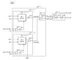
본 발명의 실시예에 따른 반도체 메모리 장치는 도 1에 도시된 바와 같이, 지연 고정 루프 회로(100), 동기 신호 생성부(200), 직병렬 데이터 변환부(300), 및 데이터 저장 영역(400)을 포함한다.As illustrated in FIG. 1, a semiconductor memory device according to an exemplary embodiment of the present invention may include a delay locked
상기 지연 고정 루프 회로(100)는 외부에서 제공되는 외부 클럭(CLK)을 입력 클럭으로 입력 받아 지연 고정 클럭 신호(DLL_CLK)을 생성한다. 상기 지연 고정 루프 회로(100)는 일반적인 DLL(delay locked loop) 회로로 구성될 수 있다.The delay locked
상기 동기 신호 생성부(200)는 라이트 동작시 제어 신호(MRS)에 응답하여 데이터 입출력 스트로브 신호(DQS) 또는 상기 지연 고정 클럭 신호(DLL_CLK)를 동기 신호(Dsr, Dsf)로서 출력한다. 이때, 상기 제어 신호(MRS)는 모드 레지스터 셋(mode register set)의 출력 신호로서, 모드 레지스터 셋에 저장된 기설정된 정보이다. 또한 상기 제어 신호(MRS)는 테스트시 이용되는 테스트 신호일 수도 있고, 퓨즈의 커팅 여부에 따라 그 레벨이 변하는 신호 즉, 일반적인 퓨즈 회로의 출력 신호일 수 있다. 본 발명에서는 상기 제어 신호(MRS)가 모드 레지스터 셋의 출력 신호인 것을 실시예로 개시할 뿐, 상기 제어 신호(MRS)가 모드 레지스터 셋의 출력 신호인 것만을 한정하는 것은 아니다.The
상기 동기 신호 생성부(200)는 드라이버(210), 예비 동기 신호 생성부(220), 및 데이터 동기 신호 생성부(230)를 포함한다.The
상기 드라이버(210)는 데이터 입출력 스트로브 신호(DQS)를 드라이빙하여 제 1 라이징 예비 동기 신호(Dsr_p1), 및 제 1 폴링 예비 동기 신호(Dsf_p1)를 생성한다. 이때, 상기 제 1 라이징 예비 동기 신호(Dsr_p1), 및 상기 제 1 폴링 예비 동기 신호(Dsf_p1)의 위상은 서로 반대이다.The
상기 예비 동기 신호 생성부(220)는 주파수 감지 신호(Low_Frq_det), 라이트 레이턴시(WL, write latency), 리드 레이턴시(RL, read latency), 및 상기 제어 신호(MRS)에 응답하여 액티브 신호(ACT), 리드 신호(RD), 및 라이트 신호(WT) 중 하나의 인에이블 타이밍에 상기 지연 고정 클럭 신호(DLL_CLK)를 제 2 라이징 예비 동기 신호(Dsr_p2), 및 제 2 폴링 예비 동기 신호(Dsf_p2)로서 출력한다. 이때, 상기 제 2 라이징 예비 동기 신호(Dsr_p2)와 상기 제 2 폴링 예비 동기 신호(Dsf_p2)의 위상은 서로 반대 위상이다.The preliminary
예를 들어, 상기 예비 동기 신호 생성부(220)는 리드 동작시 상기 주파수 감지 신호(Low_Frq_det) 및 상기 리드 레이턴시 신호(RL)에 응답하여 상기 액티브 신호(ACT) 또는 상기 리드 신호(RD)의 인에이블 타이밍에 상기 지연 고정 클럭 신호(DLL_CLK)를 상기 제 2 라이징 예비 동기 신호(Dsr_p2), 및 상기 제 2 폴링 예비 동기 신호(Dsf_p2)로서 출력한다. 또한, 상기 예비 동기 신호 생성부(220)는 라이트 동작시 상기 제어 신호(MRS)가 인에이블되면 상기 주파수 감지 신호(Low_frq_det) 및 상기 라이트 레이턴시 신호(WL)에 응답하여 상기 액티브 신호(ACT) 또는 상기 라이트 신호(WT)의 인에이블 타이밍에 상기 지연 고정 클럭 신호(DLL_CLK)를 상기 제 2 라이징 예비 동기 신호(Dsr_p2), 및 상기 제 2 폴링 예비 동기 신호(Dsf_p2)로서 출력한다.For example, the preliminary
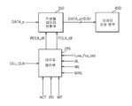
상기 예비 동기 신호 생성부(220)는 타이밍 제어부(221), 및 출력 제어부(222)를 포함한다.The preliminary
상기 타이밍 제어부(221)는 상기 주파수 감지 신호(Low_Frq_det), 상기 리드 레이턴시 신호(RL), 및 상기 제어 신호(MRS)에 응답하여 상기 액티브 신호(ACT)의 인에이블 타이밍 또는 상기 리드 신호(RD) 및 상기 라이트 신호(WT)의 인에이블 타이밍에 상기 지연 고정 클럭 신호(DLL_CLK)를 지연 고정 라이징 클럭 신호(RCLK_dll), 및 지연 고정 폴링 클럭 신호(FCLK_dll)로서 출력한다. 예를 들어, 상기 타이밍 제어부(221)는 상기 주파수 감지 신호(Low_Frq_det)가 인에이블되거나 상기 리드 레이턴시 신호(RL)의 레이턴시 값이 기설정된 레이턴시 값이상이면 상기 액티브 신호(ACT)의 인에이블 타이밍에 상기 지연 고정 클럭 신호(DLL_CLK)을 상기 지연 고정 라이징 클럭 신호(RCLK_dll) 및 상기 지연 고정 폴링 클럭 신호(FCLK_dll)로서 출력한다. 상기 타이밍 제어부(221)는 상기 주파수 감지 신호(Low_Frq_det)가 디스에이블되고 상기 리드 레이턴시 신호(RL)의 레이턴시 값이 상기 기설정된 레이턴시 값이하이면 상기 리드 신호(RD)의 인에이블 타이밍에 상기 지연 고정 클럭 신호(DLL_CLK)를 상기 지연 고정 라이징 클럭 신호(RCLK_dll) 및 상기 지연 고정 폴링 클럭 신호(FCLK_dll)으로서 출력한다. 한편, 상기 타이밍 제어부(221)는 상기 제어 신호(MRS)가 인에이블되고 상기 주파수 감지 신호(Low_Frq_det)가 인에이블되거나 상기 라이트 레이턴시 신호(WL)의 레이턴시 값이 기설정된 레이턴시 값이상이면 상기 액티브 신호(ACT)의 인에이블 타이밍에 상기 지연 고정 클럭 신호(DLL_CLK)을 상기 지연 고정 라이징 클럭 신호(RCLK_dll), 및 상기 지연 고정 폴링 클럭 신호(FCLK_dll)으로서 출력한다. 상기 타이밍 제어부(221)는 상기 제어 신호(MRS)가 인에이블되고 상기 주파수 감지 신호(Low_Frq_det)가 디스에이블되며 상기 라이트 레이턴시 신호(WL)의 레이턴시 값이 상기 기설정된 레이턴시 값이하이면 상기 라이트 신호(WT)의 인에이블 타이밍에 상기 지연 고정 클럭 신호(DLL_CLK)을 상기 지연 고정 라이징 클럭 신호(RCLK_dll) 및 상기 지연 고정 폴링 클럭 신호(FCLK_dll)로서 출력한다. 또한, 상기 타이밍 제어부(221)는 상기 제어 신호(MRS)가 디스에이블되면 라이트 동작시 상기 지연 고정 클럭 신호(DLL_CLK)를 상기 지연 고정 라이징 클럭 신호(RCLK_dll) 및 상기 지연 고정 폴링 클럭 신호(FCLK_dll)로서 제공하지 않는다.The
상기 타이밍 제어부(221)는 도 2에 도시된 바와 같이, 출력 인에이블 신호 생성부(221-1), 및 출력부(221-2)를 포함한다.As illustrated in FIG. 2, the
상기 출력 인에이블 신호 생성부(221-1)는 상기 주파수 감지 신호(Low_Frq_det), 상기 리드 레이턴시 신호(RL), 상기 라이트 레이턴시 신호(WL), 및 상기 제어 신호(MRS)에 응답하여 상기 액티브 신호(ACT)의 인에이블 타이밍 또는 상기 리드 신호(RD) 및 상기 라이트 신호(WT)의 인에이블 타이밍에 인에이블되는 출력 인에이블 신호(OUT_en)를 생성한다.The output enable signal generator 221-1 may generate the active signal in response to the frequency detection signal Low_Frq_det, the read latency signal RL, the write latency signal WL, and the control signal MRS. An output enable signal OUT_en that is enabled at an enable timing of the ACT or an enable timing of the read signal RD and the write signal WT is generated.
상기 출력 인에이블 신호 생성부(221-1)는 제 1 신호 생성부(221-1-1), 제 2 신호 생성부(221-1-2), 및 신호 조합부(221-1-3)를 포함한다.The output enable signal generator 221-1 includes a first signal generator 221-1-1, a second signal generator 221-1-2, and a signal combiner 221-1-3. It includes.
상기 제 1 신호 생성부(221-1-1)는 상기 주파수 감지 신호(Low_Frq_det), 및 상기 리드 레이턴시 신호(RL)에 응답하여 상기 액티브 신호(ACT) 또는 상기 리드 신호(RD)를 제 1 타이밍 신호(t_signalA)로서 출력한다. 예를 들어, 상기 제 1 신호 생성부(221-1-1)는 상기 주파수 감지 신호(Low_Frq_det)가 인에이블되거나 상기 리드 레이턴시 신호(RL)가 인에이블되면 상기 액티브 신호(ACT)를 상기 제 1 타이밍 신호(t_signalA)로서 출력하고, 상기 주파수 감지 신호(Low_Frq_det)가 디스에이블되고 상기 리드 레이턴시 신호(RL)가 디스에이블되면 상기 리드 신호(RD)를 상기 제 1 타이밍 신호(t_signalA)로서 출력한다. 이때, 상기 주파수 감지 신호(Low_Frq_det)는 반도체 메모리 장치에 입력되는 외부 클럭의 주파수가 기설정된 주파수이상이면 로우 레벨로 인에이블되고, 상기 기설정된 주파수 이하이면 하이 레벨로 디스에이블되는 신호이다. 또한 상기 리드 레이턴시 신호(RL)는 반도체 메모리 장치에 리드 명령이 입력되고 외부 클럭의 기설정된 주기가 경과하면 인에이블되는 신호로, 상기 리드 레이턴시 신호(RL)의 레이턴시 값이 증가할수록 외부 클럭의 기설정된 주기 값이 증가한다.The first signal generator 221-1-1 may first timing the active signal ACT or the read signal RD in response to the frequency detection signal Low_Frq_det and the read latency signal RL. Output as signal t_signalA. For example, when the frequency detection signal Low_Frq_det is enabled or the read latency signal RL is enabled, the first signal generator 221-1-1 transmits the active signal ACT to the first signal. When the frequency detection signal Low_Frq_det is disabled and the read latency signal RL is disabled, the read signal RD is output as the first timing signal t_signalA. In this case, the frequency detection signal Low_Frq_det is a signal that is enabled at a low level when the frequency of the external clock input to the semiconductor memory device is greater than or equal to a preset frequency, and is disabled by a high level if less than or equal to the preset frequency. Also, the read latency signal RL is a signal that is enabled when a read command is input to the semiconductor memory device and a predetermined period of the external clock has elapsed. The read latency signal RL increases as the latency value of the read latency signal RL increases. The set period value is increased.
상기 제 1 신호 생성부(221-1-1)는 제 1 낸드 게이트(ND11), 제 1 및 제 2 인버터(IV11, IV12), 및 제 1 선택부(221-1-1-1)를 포함한다. 상기 제 1 낸드 게이트(ND11)는 상기 주파수 감지 신호(Low_Frq_det) 및 상기 리드 레이턴시 신호(RL)를 입력 받는다. 상기 제 1 인버터(IV11)는 상기 제 1 낸드 게이트(ND11)의 출력 신호를 입력 받는다. 상기 제 1 선택부(221-1-1-1)는 상기 제 1 인버터(IV11)의 출력 신호가 로우 레벨이면 상기 액티브 신호(ACT)를 출력하고, 상기 제 1 인버터(IV11)의 출력 신호가 하이 레벨이면 상기 리드 신호(RD)를 출력한다. 상기 제 1 선택부(221-1-1-1)는 멀티 플렉서로 구현 가능하다. 상기 제 2 인버터(IV12)는 상기 제 1 선택부(221-1-1-1)의 출력 신호를 입력 받아 상기 제 1 타이밍 신호(t_signalA)를 출력한다.The first signal generator 221-1-1 includes a first NAND gate ND11, first and second inverters IV11 and IV12, and a first selector 221-1-1-1. do. The first NAND gate ND11 receives the frequency detection signal Low_Frq_det and the read latency signal RL. The first inverter IV11 receives the output signal of the first NAND gate ND11. The first selector 221-1-1-1 outputs the active signal ACT when the output signal of the first inverter IV11 is at a low level, and output signal of the first inverter IV11 is output. If the read level is high, the read signal RD is output. The first selector 221-1-1-1 may be implemented as a multiplexer. The second inverter IV12 receives the output signal of the first selector 221-1-1-1 and outputs the first timing signal t_signalA.
상기 제 2 신호 생성부(221-1-2)는 상기 제어 신호(MRS)가 인에이블되면 상기 주파수 감지 신호(Low_Frq_det), 및 상기 라이트 레이턴시 신호(WL)에 응답하여 상기 액티브 신호(ACT) 또는 상기 라이트 신호(WT)를 제 2 타이밍 신호(t_signalB)로서 출력한다. 예를 들어, 상기 제 2 신호 생성부(221-1-2)는 상기 제어 신호(MRS)가 인에이블되고 상기 주파수 감지 신호(Low_Frq_det)가 인에이블되거나 상기 라이트 레이턴시 신호(WL)가 인에이블되면 상기 액티브 신호(ACT)를 상기 제 2 타이밍 신호(t_signalB)로서 출력하고, 상기 주파수 감지 신호(Low_Frq_det)가 디스에이블되고 상기 라이트 레이턴시 신호(WL)가 디스에이블되면 상기 라이트 신호(WT)를 상기 제 2 타이밍 신호(t_signalB)로서 출력한다. 이때, 상기 주파수 감지 신호(Low_Frq_det)는 반도체 메모리 장치에 입력되는 외부 클럭의 주파수가 기설정된 주파수이상이면 로우 레벨로 인에이블되고, 상기 기설정된 주파수 이하이면 하이 레벨로 디스에이블되는 신호이다. 또한 상기 라이트 레이턴시 신호(WL)는 반도체 메모리 장치에 라이트 명령이 입력되고 외부 클럭의 기설정된 주기가 경과하면 인에이블되는 신호로, 상기 라이트 레이턴시 신호(WL)의 레이턴시 값이 증가할수록 외부 클럭의 기설정된 주기 값이 증가한다.When the control signal MRS is enabled, the second signal generator 221-1-2 responds to the frequency detection signal Low_Frq_det and the write latency signal WL in response to the active signal ACT or The write signal WT is output as the second timing signal t_signalB. For example, when the control signal MRS is enabled and the frequency detection signal Low_Frq_det is enabled or the write latency signal WL is enabled, the second signal generator 221-1-2 is enabled. The active signal ACT is output as the second timing signal t_signalB, and when the frequency detection signal Low_Frq_det is disabled and the write latency signal WL is disabled, the write signal WT is output to the second signal. 2 It is output as a timing signal t_signalB. In this case, the frequency detection signal Low_Frq_det is a signal that is enabled at a low level when the frequency of the external clock input to the semiconductor memory device is greater than or equal to a preset frequency, and is disabled by a high level if less than or equal to the preset frequency. The write latency signal WL is a signal that is enabled when a write command is input to a semiconductor memory device and a predetermined period of an external clock elapses. The write latency signal WL increases as the latency value of the write latency signal WL increases. The set period value is increased.
상기 제 2 신호 생성부(221-1-2)는 제 2 및 제 3 낸드 게이트(ND12, ND13), 제 3 인버터(IV13), 및 제 2 선택부(221-1-2-1)를 포함한다. 상기 제 2 낸드 게이트(ND12)는 상기 주파수 감지 신호(Low_Frq_det) 및 상기 라이트 레이턴시 신호(WL)를 입력 받는다. 상기 제 3 인버터(IV13)는 상기 제 2 낸드 게이트(ND12)의 출력 신호를 입력 받는다. 상기 제 2 선택부(221-1-2-1)는 상기 제 3 인버터(IV13)의 출력 신호가 로우 레벨이면 상기 액티브 신호(ACT)를 출력하고, 상기 제 3 인버터(IV13)의 출력 신호가 하이 레벨이면 상기 라이트 신호(WT)를 출력한다. 상기 제 2 선택부(221-1-2-1)는 멀티 플렉서로 구현 가능하다. 상기 제 3 낸드 게이트(ND13)는 상기 제어 신호(MRS)가 하이 레벨로 인에이블되면 상기 제 상기 제 2 선택부(221-1-2-1)의 출력 신호를 입력 받아 상기 제 2 타이밍 신호(t_signalB)를 출력한다. 또한 상기 제 3 낸드 게이트(ND13)는 상기 제어 신호(MRS)가 로우 레벨로 디스에이블되면 상기 제 2 타이밍 신호(t_signalB)를 로우 레벨로 고정시킨다.The second signal generator 221-1-2 includes second and third NAND gates ND12 and ND13, a third inverter IV13, and a second selector 221-1-2-1. do. The second NAND gate ND12 receives the frequency sensing signal Low_Frq_det and the write latency signal WL. The third inverter IV13 receives the output signal of the second NAND gate ND12. The second selector 221-1-2-1 outputs the active signal ACT when the output signal of the third inverter IV13 is at a low level, and output signal of the third inverter IV13 is output. If the level is high, the write signal WT is output. The second selector 221-1-2-1 may be implemented as a multiplexer. The third NAND gate ND13 receives the output signal of the second selector 221-1-2-1 when the control signal MRS is enabled at a high level. t_signalB) The third NAND gate ND13 fixes the second timing signal t_signalB to a low level when the control signal MRS is disabled to a low level.
상기 신호 조합부(221-1-3)는 상기 제 1 타이밍 신호(t_signalA), 및 상기 제 2 타이밍 신호(t_signalB) 중 하나라도 로우 레벨로 인에이블되면 하이 레벨로 인에이블된 상기 출력 인에이블 신호(OUT_en)를 생성한다.The signal combination unit 221-1-3 may enable the output enable signal enabled at a high level when any one of the first timing signal t_signalA and the second timing signal t_signalB is enabled at a low level. Create (OUT_en).
상기 신호 조합부(221-1-3)는 제 4 낸드 게이트(ND14)를 포함한다. 상기 제 4 낸드 게이트(ND14)는 상기 제 1 및 제 2 타이밍 신호(t_gisnalA, t_signalB)를 입력 받아 상기 출력 인에이블 신호(OUT_en)를 출력한다.The signal combination unit 221-1-3 includes a fourth NAND gate ND14. The fourth NAND gate ND14 receives the first and second timing signals t_gisnalA and t_signalB and outputs the output enable signal OUT_en.
상기 출력부(221-2)는 상기 출력 인에이블 신호(OUT_en)가 하이 레벨로 인에이블되면 상기 지연 고정 클럭 신호(DLL_CLK)를 상기 지연 고정 라이징 클럭 신호(RCLK_dll), 및 상기 지연 고정 폴링 클럭 신호(FCLK_dll)로서 출력하고, 상기 출력 인에이블 신호(OUT_en)가 로우 레벨로 디스에이블되면 상기 지연 고정 라이징 클럭 신호(RCLK_dll)를 로우 레벨로 고정시키고, 상기 지연 고정 폴링 클럭 신호(FCLK_dll)를 하이 레벨로 고정시킨다.The output unit 221-2 may output the delayed fixed clock signal DLL_CLK to the delayed fixed rising clock signal RCLK_dll and the delayed fixed polling clock signal when the output enable signal OUT_en is enabled at a high level. Outputs as FCLK_dll, and when the output enable signal OUT_en is disabled at a low level, fixes the delayed fixed rising clock signal RCLK_dll to a low level and sets the delayed fixed polling clock signal FCLK_dll to a high level. Secure with.
상기 출력부(221-2)는 제 5 낸드 게이트(ND15), 및 제 4 및 제 5 인버터(IV14, IV15)를 포함한다. 상기 제 5 낸드 게이트(ND15)는 상기 지연 고정 클럭 신호(DLL_CLK), 및 상기 출력 인에이블 신호(OUT_en)를 입력 받는다. 상기 제 4 인버터(IV14)는 상기 제 5 낸드 게이트(ND15)의 출력 신호를 입력 받아 상기 지연 고정 라이징 클럭 신호(RCLK_dll)를 출력한다. 상기 제 5 인버터(IV15)는 상기 제 4 인버터(IV14)의 출력 신호를 입력 받아 상기 지연 고정 폴링 클럭 신호(FCLK_dll)를 출력한다.The output unit 221-2 includes a fifth NAND gate ND15, and fourth and fifth inverters IV14 and IV15. The fifth NAND gate ND15 receives the delay locked clock signal DLL_CLK and the output enable signal OUT_en. The fourth inverter IV14 receives the output signal of the fifth NAND gate ND15 and outputs the delayed fixed rising clock signal RCLK_dll. The fifth inverter IV15 receives the output signal of the fourth inverter IV14 and outputs the delayed fixed polling clock signal FCLK_dll.
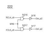
상기 출력 제어부(222)는 상기 제어 신호(MRS)가 하이 레벨로 인에이블되면 상기 지연 고정 라이징 클럭 신호(RCLK_dll) 및 상기 지연 고정 폴링 클럭 신호(FCLK_dll) 각각을 상기 제 2 라이징 예비 동기 신호(Dsr_p2), 및 상기 제 2 폴링 예비 동기 신호(Dsf_p2)로서 출력하고, 상기 제어 신호(MRS)가 로우 레벨로 디스에이블되면 상기 제 2 라이징 예비 동기 신호(Dsr_p2) 및 상기 제 2 폴링 예비 동기 신호(Dsf_p2)를 특정 레벨 즉, 로우 레벨로 고정시킨다.When the control signal MRS is enabled at the high level, the
상기 출력 제어부(222)는 제 6 및 제 7 낸드 게이트(ND16, ND17), 및 제 6 및 제 7 인버터(IV16, IV17)를 포함한다. 상기 제 6 낸드 게이트(ND16)는 상기 지연 고정 라이징 클럭 신호(RCLK_dll) 및 상기 제어 신호(MRS)를 입력 받는다. 상기 제 7 낸드 게이트(ND17)는 상기 지연 고정 폴링 클럭 신호(FCLK_dll) 및 상기 제어 신호(MRS)를 입력 받는다. 상기 제 6 인버터(IV16)는 상기 제 6 낸드 게이트(ND16)의 출력 신호를 입력 받아 상기 제 2 라이징 예비 동기 신호(Dsr_p2)를 출력한다. 상기 제 7 인버터(IV17)는 상기 제 7 낸드 게이트(ND17)의 출력 신호를 입력 받아 상기 제 2 폴링 예비 동기 신호(Dsf_p2)를 출력한다.The
상기 데이터 동기 신호 생성부(230)는 상기 제어 신호(MRS)에 응답하여 상기 제 1 라이징 예비 동기 신호(Dsr_p1) 및 상기 제 1 폴링 예비 동기 신호(Drf_p1) 또는 상기 제 2 라이징 예비 동기 신호(Dsr_p2), 및 상기 제 2 폴링 예비 동기 신호(Dsf_p2)를 상기 라이징 동기 신호(Dsr), 및 상기 폴링 동기 신호(Dsf)로서 출력한다. 예를 들어, 상기 데이터 동기 신호 생성부(230)는 상기 제어 신호(MRS)가 디스에이블되면 상기 제 1 라이징 예비 동기 신호(Dsr_p1)를 상기 라이징 동기 신호(Dsr)로서 출력하고, 상기 제 1 폴링 예비 동기 신호(Dsr_p1)를 상기 폴링 동기 신호(Dsf)로서 출력한다. 또한, 상기 데이터 동기 신호 생성부(230)는 상기 제어 신호(MRS)가 인에이블되면 상기 제 2 라이징 예비 동기 신호(Dsr_p2)를 상기 라이징 동기 신호(Dsr)로서 출력하고, 상기 제 2 폴링 예비 동기 신호(Dsf_p2)를 상기 폴링 동기 신호(Dsf)로서 출력한다.The data synchronizing
상기 데이터 동기 신호 생성부(230)는 도 4에 도시된 바와 같이, 라이징 동기 신호 생성부(231), 및 폴링 동기 신호 생성부(232)를 포함한다.As illustrated in FIG. 4, the data
상기 라이징 동기 신호 생성부(231)는 상기 제어 신호(MRS)가 디스에이블되면 상기 제 1 라이징 예비 동기 신호(Dsr_p1)를 상기 라이징 동기 신호(Dsr)로서 출력하고, 상기 제어 신호(MRS)가 인에이블되면 상기 제 2 라이징 예비 동기 신호(Dsr_p2)를 상기 라이징 동기 신호(Dsr)로서 출력한다.The rising
상기 라이징 동기 신호 생성부(231)는 제 8 내지 제 10 낸드 게이트(ND18, ND19, ND20), 및 제 8 인버터(IV18)를 포함한다. 상기 제 8 낸드 게이트(ND18)는 상기 제어 신호(MRS) 및 상기 제 2 라이징 예비 동기 신호(Dsr_p2)를 입력 받는다. 상기 제 8 인버터(IV18)는 상기 제어 신호(MRS)를 입력 받는다. 상기 제 9 낸드 게이트(ND19)는 상기 제 1 라이징 예비 동기 신호(Dsr_p1) 및 상기 제 8 인버터(IV18)의 출력 신호를 입력 받는다. 상기 제 10 낸드 게이트(ND20)는 상기 제 9 및 제 10 낸드 게이트(ND18, ND19)의 출력 신호를 입력 받아 상기 라이징 동기 신호(Dsr)를 출력한다.The rising
상기 폴링 동기 신호 생성부(232)는 상기 제어 신호(MRS)가 디스에이블되면 상기 제 1 폴링 예비 동기 신호(Dsf_p1)를 상기 폴링 동기 신호(Dsf)로서 출력하고, 상기 제어 신호(MRS)가 인에이블되면 상기 제 2 폴링 예비 동기 신호(Dsf_p2)를 상기 폴링 동기 신호(Dsf)로서 출력한다.The polling
상기 폴링 동기 신호 생성부(232)는 제 11 내지 제 13 낸드 게이트(ND21, ND22, ND23), 및 제 9 인버터(IV19)를 포함한다. 상기 제 11 낸드 게이트(ND21)는 상기 제어 신호(MRS) 및 상기 제 2 폴링 예비 동기 신호(Dsf_p2)를 입력 받는다. 상기 제 9 인버터(IV19)는 상기 제어 신호(MRS)를 입력 받는다. 상기 제 12 낸드 게이트(ND22)는 상기 제 1 폴링 예비 동기 신호(Dsf_p1) 및 상기 제 9 인버터(IV19)의 출력 신호를 입력 받는다. 상기 제 13 낸드 게이트(ND23)는 상기 제 11 및 제 12 낸드 게이트(ND21, ND22)의 출력 신호를 입력 받아 상기 폴링 동기 신호(Dsf)를 출력한다.The polling
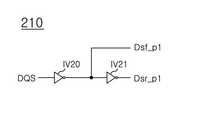
도 1에 도시된 상기 드라이버(210)는 도 5에 도시된 바와 같이, 제 10 및 제 11 인버터(IV20, IV21)를 포함할 수 있다. 상기 제 10 인버터(IV20)는 상기 데이터 입출력 스트로브 신호(DQS)를 입력 받아 상기 제 1 폴링 예비 동기 신호(Dsf_p1)를 출력한다. 상기 제 11 인버터(IV21)는 상기 제 10 인버터(IV20)의 출력 신호를 입력 받아 상기 제 1 라이징 예비 동기 신호(Dsr_p1)를 출력한다.As shown in FIG. 5, the
도 1에 도시된 상기 직병렬 데이터 변환부(300)는 도 6에 도시된 바와 같이, 제 1 내지 제 7 플립플롭(FF11~FF17), 및 제 1 내지 제 4 지연부(310~340)를 포함할 수 있다. 상기 제 1 내지 제 4 플립플롭(FF11~FF14)은 직렬로 연결된다. 상기 제 5 내지 제 7 플립플롭(FF15~FF17)은 직렬로 연결된다. 더 상세히 설명하면, 상기 제 1 플립플롭(FF11)은 상기 라이징 동기 신호(Dsr)에 응답하여 상기 직렬 데이터(DATA_s)를 입력 및 저장하고 출력한다. 상기 제 2 플립플롭(FF12)은 상기 폴링 동기 신호(Dsf)에 응답하여 상기 제 1 플립플롭(FF11)의 출력 신호를 입력 및 저장하고 출력한다. 상기 제 3 플립플롭(FF13)은 상기 라이징 동기 신호(Dsr)에 응답하여 상기 제 2 플립플롭(FF12)의 출력 신호를 입력 및 저장하고 출력한다. 상기 제 4 플립플롭(FF14)은 상기 폴링 동기 신호(Dsf)에 응답하여 상기 제 3 플립플롭(FF13)의 출력 신호를 입력 및 저장하고 출력한다. 상기 제 5 플립플롭(FF15)은 상기 폴링 동기 신호(Dsf)에 응답하여 상기 직렬 데이터(DATA_s)를 입력 및 저장하고 출력한다. 상기 제 6 플립플롭(FF16)은 상기 라이징 동기 신호(Dsr)에 응답하여 상기 제 5 플립플롭(FF15)의 출력 신호를 입력 및 저장하고 출력한다. 상기 제 7 플립플롭(FF17)은 상기 폴링 동기 신호(Dsf)에 응답하여 상기 제 6 플립플롭(FF16)의 출력 신호를 입력 및 저장하고 출력한다. 상기 제 1 지연부(310)는 상기 제 2 플립플롭(FF12)의 출력 신호를 지연시켜 상기 병렬 데이터(DATA_p<0>)로서 출력한다. 상기 제 2 지연부(320)는 상기 제 4 플립플롭(FF14)의 출력 신호를 지연시켜 상기 병렬 데이터(DATA_p<1>)로서 출력한다. 상기 제 3 지연부(330)는 상기 제 7 플립플롭(FF17)의 출력 신호를 지연시켜 상기 병렬 데이터(DATA_p<2>)로서 출력한다. 상기 제 4 지연부(340)는 상기 제 5 플립플롭(FF15)의 출력 신호를 지연시켜 상기 병렬 데이터(DATA_p<3>)로서 출력한다. 이때, 상기 제 1 내지 제 4 지연부(310~340)의 각 지연값은 상기 병렬 데이터(DATA_p<0:3>)의 각 비트가 동시에 출력되도록 결정된다.As shown in FIG. 6, the serial-to-
이와 같이 구성된 본 발명의 실시예에 따른 반도체 메모리 장치는 다음과 같이 동작한다.The semiconductor memory device according to the embodiment of the present invention configured as described above operates as follows.
반도체 메모리 장치의 동작 모드를 설정하기 위하여, 모드 레지스터 셋(mode register set)에 제어 신호(MRS)를 하이 레벨로 설정하거나, 로우 레벨로 설정한다. 이때, 상기 제어 신호(MRS)를 하이 레벨로 설정하는 것은 지연 고정 클럭 신호(DLL_CLK)를 이용하여 직렬 데이터(DATA_s)를 병렬 데이터(DATA_p<0:3>)로 변환하는 모드를 설정한 것이다.In order to set the operation mode of the semiconductor memory device, the control signal MRS is set to a high level or a low level in a mode register set. In this case, setting the control signal MRS to the high level is a mode of converting serial data DATA_s into parallel data DATA_p <0: 3> using the delayed fixed clock signal DLL_CLK.
상세히 설명하면, 지연 고정 루프 회로(100)는 상기 지연 고정 클럭 신호(DLL_CLK)를 생성한다.In detail, the delay locked
타이밍 제어부(221)는 상기 지연 고정 클럭 신호(DLL_CLK)가 지연 고정 라이징 클럭 신호(RCLK_dll) 및 지연 고정 폴링 클럭 신호(FCLK_dll)로서 출력되는 타이밍을 결정한다. 상기 타이밍 제어부(221)는 리드 동작시 상기 지연 고정 라이징 클럭 신호(RCLK_dll) 및 상기 지연 고정 폴링 클럭 신호(FCLK_dll)가 액티브 신호(ACT)의 인에이블 타이밍에 출력되거나, 리드 신호(RD)의 인에이블 타이밍에 출력되도록 주파수 감지 신호(Low_Frq_det) 및 리드 레이턴시(RL)에 응답하여 결정한다. 또한 상기 타이밍 제어부(221)는 상기 제어 신호(MRS)가 인에이블되면 라이트 동작시 상기 지연 고정 라이징 클럭 신호(RCLK_dll) 및 상기 지연 고정 폴링 클럭 신호(FCLK_dll)가 상기 액티브 신호(ACT)의 인에이블 타이밍에 출력되거나, 라이트 신호(WT)의 인에이블 타이밍에 출력되도록 상기 주파수 감지 신호(Low_Frq_det) 및 라이트 레이턴시(WL)에 응답하여 결정한다. 즉, 반도체 메모리 장치가 높은 주파수의 클럭을 입력 받을 때 또는 외부로부터 리드 또는 라이트 명령을 입력 받고 설정된 시간보다 빠른 리드 또는 라이트 동작이 요구될 때 상기 지연 고정 라이징 클럭 신호(RCLK_dll) 및 상기 지연 고정 폴링 클럭 신호(FCLK_dll)는 상기 액티브 신호(ACT)의 인에이블 타이밍에 출력된다.The
상기 제어 신호(MRS)가 하이 레벨이므로, 출력 제어부(222)는 상기 지연 고정 라이징 클럭 신호(RCLK_dll) 및 상기 지연 고정 폴링 클럭 신호(FCLK_dll)를 제 2 라이징 예비 동기 신호(Dsr_p2), 및 제 2 폴링 예비 동기 신호(Dsf_p2)로서 출력한다. 또한 데이터 동기 신호 생성부(230)는 제 1 라이징 예비 동기 신호(Dsr_p1), 및 제 1 폴링 예비 동기 신호(Dsf_p1)와 상기 제 2 라이징 예비 동기 신호(Dsr_p2), 및 상기 제 2 폴링 예비 동기 신호(Dsf_p2) 중 상기 제 2 라이징 예비 동기 신호(Dsr_p2), 및 상기 제 2 폴링 예비 동기 신호(Dsf_p2)를 라이징 동기 신호(Dsr) 및 폴링 동기 신호(Dsf)로서 직병렬 데이터 변환부(300)에 제공한다.Since the control signal MRS is at a high level, the
상기 직병렬 데이터 변환부(300)는 상기 라이징 동기 신호(Dsr) 및 상기 폴링 동기 신호(Dsf)에 응답하여 직렬 데이터(DATA_s)를 병렬 데이터(DATA_p<0:3>)로 변환한다.The serial-to-
상기 병렬 데이터(DATA_p<0:3>)는 데이터 저장 영역(400)에 저장된다.The parallel data DATA_p <0: 3> is stored in the
한편, 상기 제어 신호(MRS)가 로우 레벨이면, 상기 출력 제어부(222)는 로우 레벨로 고정된 상기 제 2 라이징 예비 동기 신호(Dsr_p2), 및 상기 제 2 폴링 예비 동기 신호(Dsf_p2)를 출력한다.On the other hand, if the control signal MRS is at the low level, the
상기 데이터 동기 신호 생성부(230)는 상기 제 1 라이징 예비 동기 신호(Dsr_p1), 및 상기 제 1 폴링 예비 동기 신호(Dsf_p1)와 상기 제 2 라이징 예비 동기 신호(Dsr_p2), 및 상기 제 2 폴링 예비 동기 신호(Dsf_p2) 중 상기 제 1 라이징 예비 동기 신호(Dsr_p1), 및 상기 제 1 폴링 예비 동기 신호(Dsf_p1)를 상기 라이징 동기 신호(Dsr) 및 상기 폴링 동기 신호(Dsf)로서 상기 직병렬 데이터 변환부(300)에 제공한다. 이때, 상기 제 1 라이징 예비 동기 신호(Dsr_p1), 및 상기 제 1 폴링 예비 동기 신호(Dsf_p1)는 외부에서 입력되는 데이터 입출력 스트로브 신호(DQS)에 의해 생성된다.The data
상기 직병렬 데이터 변환부(300)는 상기 라이징 동기 신호(Dsr) 및 상기 폴링 동기 신호(Dsf)에 응답하여 직렬 데이터(DATA_s)를 병렬 데이터(DATA_p<0:3>)로 변환한다.The serial-to-
결국, 상기 제어 신호(MRS)가 하이 레벨일 경우 상기 지연 고정 클럭(DLL_CLK)으로 상기 직렬 데이터(DATA_s)를 상기 병렬 데이터(DATA_p<0:3>)로 변환하고, 상기 제어 신호(MRS)가 로우 레벨일 경우 상기 직렬 데이터(DATA_s)를 상기 병렬 데이터(DATA_p<0:3>)로 변환한다.As a result, when the control signal MRS is at the high level, the serial data DATA_s is converted into the parallel data DATA_p <0: 3> using the delay locked clock DLL_CLK, and the control signal MRS is In the low level, the serial data DATA_s is converted into the parallel data DATA_p <0: 3>.
본 발명에 따른 반도체 메모리 장치는 외부로부터 데이터를 입력 받아 저장할 경우 즉, 라이트 동작시 외부로부터 입력되는 데이터 입출력 스트로브 신호(DQS)를 이용할 수 있고, 또한 내부로부터 생성되는 지연 고정 클럭 신호(DLL_CLK)를 이용할 수도 있다.The semiconductor memory device according to the present invention can use the data input / output strobe signal DQS that is input from the outside when receiving and storing data from the outside, that is, during a write operation, and also receives the delayed fixed clock signal DLL_CLK generated from the inside. It can also be used.
그러므로, 테스트시 또는 테스트시가 아닌 노멀 동작시 외부로부터 신호를 입력 받는 패드(PAD), 및 핀(PIN)의 개수를 모드 레지스터 셋에 저장된 제어 신호(MRS)를 이용하여 줄이거나 늘일 수 있다. 또한, 종래 기술에 비해 적은 개수의 채널을 이용하여 테스트시 노멀 동작시와 동일한 속도로 데이터를 입력 및 저장할 수도 있다.Therefore, the number of pads PAD and pins that receive a signal from an external source during a test or a non-test normal operation may be reduced or increased by using the control signal MRS stored in the mode register set. In addition, using a smaller number of channels than the prior art, data may be input and stored at the same speed as in the normal operation during the test.
반도체 메모리 장치 내부에 구성된 모드 레지스터 셋(mode register set)은 반도체 메모리 장치의 동작 모드를 설정할 수 있는 구성이다.The mode register set configured in the semiconductor memory device is a configuration that can set an operation mode of the semiconductor memory device.
반도체 메모리 장치가 외부에서 데이터를 입력 받아 데이터 저장 영역에 전달하는 과정에서 입력 받은 데이터 즉, 직렬 데이터(DATA_s)를 병렬 데이터(DATA_p)로 변환할 때 동기 신호를 이용한다. 본 발명은 모드 레지스터 셋을 이용하여 직렬 데이터를 병렬 데이터로 변환할 때 이용되는 동기 신호의 방식을 선택할 수 있도록 구성된 것이다. 또한 본 발명은 모드 레지스터 셋 이외에 반도체 메모리 장치의 동작 모드를 설정하기 위하여 이용되는 테스트 신호 및 퓨즈 회로를 이용할 수 있음을 밝혀둔다.A synchronization signal is used when the semiconductor memory device converts the received data, that is, serial data DATA_s into parallel data DATA_p while receiving data from the outside and transferring the data to the data storage area. The present invention is configured to select a method of a synchronization signal used when converting serial data into parallel data using a mode register set. It is also noted that the present invention can utilize test signals and fuse circuits used to set the operation mode of the semiconductor memory device in addition to the mode register set.
본 발명의 다른 실시예에 따른 반도체 메모리 장치는 도 7에 도시된 바와 같이, 타이밍 제어부(250), 직병렬 데이터 변환부(350), 및 데이터 저장 영영(450)을 포함할 수 있다.As illustrated in FIG. 7, a semiconductor memory device according to another embodiment of the present invention may include a
상기 타이밍 제어부(250)는 주파수 감지 신호(Low_Frq_det), 리드 레이턴시 신호(RL), 및 제어 신호(MRS)에 응답하여 액티브 신호(ACT)의 인에이블 타이밍에 지연 고정 클럭 신호(DLL_CLK)를 지연 고정 라이징 클럭 신호(RCLK_dll) 및 지연 고정 폴링 클럭 신호(FCLK_dll)로서 출력하거나, 리드 신호(RD) 및 라이트 신호(WT)의 인에이블 타이밍에 상기 지연 고정 클럭 신호(DLL_CLK)를 상기 지연 고정 라이징 클럭 신호(RCLK_dll) 및 상기 지연 고정 폴링 클럭 신호(FCLK_dll)로서 출력한다. 즉, 상기 타이밍 제어부(250)는 상기 지연 고정 클럭 신호(DLL_CLK)를 상기 지연 고정 라이징 클럭 신호(RCLK_dll) 및 상기 지연 고정 폴링 클럭 신호(FCLK_dll)로서 출력하는 타이밍을 제어한다. 이때, 상기 주파수 감지 신호(Low_Frq_det)는 반도체 메모리 장치가 입력받는 외부 클럭 또는 상기 지연 고정 클럭 신호(DLL_CLK)의 주파수를 감지한 결과를 포함하는 신호로서, 외부 클럭 또는 상기 지연 고정 클럭 신호(DLL_CLK)이 타겟 주파수보다 높은 주파수일 경우 인에이블되는 신호이다.The
예를 들어, 상기 타이밍 제어부(250)는 주파수 감지 신호(Low_Frq_det)가 인에이블되거나 상기 리드 레이턴시 신호(RL)의 레이턴시 값이 기설정된 레이턴시 값이상이면 상기 액티브 신호(ACT)의 인에이블 타이밍에 상기 지연 고정 클럭 신호(DLL_CLK)을 상기 지연 고정 라이징 클럭 신호(RCLK_dll) 및 상기 지연 고정 폴링 클럭 신호(FCLK_dll)으로서 출력한다. 상기 타이밍 제어부(250)는 상기 주파수 감지 신호(Low_Frq_det)가 디스에이블되고 상기 리드 레이턴시 신호(RL)의 레이턴시 값이 상기 기설정된 레이턴시 값이하이면 상기 리드 신호(RD)의 인에이블 타이밍에 상기 지연 고정 클럭(DLL_CLK)을 상기 지연 고정 라이징 클럭 신호(RCLK_dll) 및 상기 지연 고정 폴링 클럭 신호(FCLK_dll)로서 출력한다. 한편, 상기 타이밍 제어부(250)는 상기 제어 신호(MRS)가 인에이블되고 상기 주파수 감지 신호(Low_Frq_det)가 인에이블되거나 상기 라이턴시 신호(WL)의 레이턴시 값이 기설정된 레이턴시 값이상이면 상기 액티브 신호(ACT)의 인에이블 타이밍에 상기 지연 고정 클럭 신호(DLL_CLK)를 상기 지연 고정 라이징 신호(RCLK_dll) 및 상기 지연 고정 폴링 신호(FCLK_dll)로서 출력한다. 상기 타이밍 제어부(250)는 상기 제어 신호(MRS)가 인에이블되고 상기 주파수 감지 신호(Low_Frq_det)가 디스에이블되며 상기 라이트 레이턴시 신호(WL)의 레이턴시 값이 상기 기설정된 레이턴시 값이하이면 상기 라이트 신호(WT)의 인에이블 타이밍에 상기 지연 고정 클럭 신호(DLL_CLK)을 상기 지연 고정 라이징 클럭 신호(RCLK_dll) 및 상기 지연 고정 폴링 클럭 신호(FCLK_dll)로서 출력한다.For example, when the frequency detection signal Low_Frq_det is enabled or the latency value of the read latency signal RL is equal to or greater than a predetermined latency value, the
상기 타이밍 제어부(250)는 도 2에 도시된 바와 같이, 본 발명의 실시예에 따른 타이밍 제어부(221)와 동일하게 출력 인에이블 신호 생성부(221-1), 및 출력부(221-2)로 구성된다. 그러므로, 상기 출력 인에이블 신호 생성부(221-1) 및 상기 출력부(221-2)의 구성 설명은 생략한다.As illustrated in FIG. 2, the
상기 직병렬 데이터 변환부(350)는 직렬 데이터(DATA_s)를 상기 지연 고정 라이징 클럭 신호(RCLK_dll) 및 상기 지연 고정 폴링 클럭 신호(FCLK_dll)에 응답하여 병렬 데이터(DATA_p<0:3>)로 변환한다. 상기 직병렬 데이터 변환부(350)는 도 6에 도시된 바와 같이, 제 1 내지 제 7 플립플롭(FF11~FF17) 및 제 1 내지 제 4 지연부(310-340)를 포함한다. 본 발명의 실시예에 따른 직병렬 데이터 변환부(300)와 도 7에 개시된 직병렬 데이터 변환부(350)는 동일하게 구성됨으로 구성 설명은 생략한다.The serial-to-
상기 데이터 저장 영역(450)는 상기 병렬 데이터(DATA_p<0:3>)를 입력 받아 저장한다.The
이와 같이 구성된 본 발명의 다른 실시예에 따른 반도체 메모리 장치는 다음과 같이 동작한다.The semiconductor memory device according to another embodiment of the present invention configured as described above operates as follows.
반도체 메모리 장치의 동작 모드를 설정하기 위하여, 모드 레지스터 셋(mode register set)에 제어 신호(MRS)를 하이 레벨 또는 로우 레벨로 설정한다. 이때, 상기 제어 신호(MRS)를 하이 레벨로 설정하는 것은 반도체 메모리 장치의 리드 동작시 및 라이트 동작시 모두 지연 고정 클럭 신호(DLL_CLK)를 이용하여 데이터를 입출력하는 모드로 설정한다는 것이다. 이때, 상기 지연 고정 클럭 신호(DLL_CLK)는 지연 고정 루프 회로(Delay Locked Loop Circuit, DLL circuit)에서 생성된 신호이다.In order to set an operation mode of the semiconductor memory device, the control signal MRS is set to a high level or a low level in a mode register set. In this case, setting the control signal MRS to a high level means that the control signal MRS is set to a mode for inputting and outputting data using the delayed fixed clock signal DLL_CLK during both the read operation and the write operation of the semiconductor memory device. In this case, the delay locked clock signal DLL_CLK is a signal generated by a delay locked loop circuit (DLL circuit).
타이밍 제어부(250)는 직병렬 데이터 변환부(350)에 제공되는 지연 고정 라이징 클럭(RCLK_dll) 및 지연 고정 폴링 클럭(FCLK_dll)의 출력 타이밍을 제어한다.The
예를 들어, 상기 타이밍 제어부(250)는 주파수 감지 신호(Low_Frq_det) 및 리드 레이턴시 신호(RL)에 응답하여 상기 지연 고정 라이징 클럭 신호(RCLK_dll) 및 상기 지연 고정 폴링 클럭 신호(FCLK_dll)가 액티브 신호(ACT)의 인에이블 타이밍에 출력되거나 리드 신호(RD)의 인에이블 타이밍에 출력되도록 동작한다. 한편, 상기 타이밍 제어부(250)는 상기 제어 신호(MRS)가 하이 레벨로 인에이블되면 라이트 동작시 상기 주파수 감지 신호(Low_Frq_det) 및 상기 라이트 리던던시 신호(WL)에 응답하여 상기 지연 고정 라이징 클럭 신호(RCLK_dll) 및 상기 지연 고정 폴링 클럭 신호(FCLK_dll)가 상기 액티브 신호(ACT)의 인에이블 타이밍에 출력되거나 라이트 신호(WT)의 인에이블 타이밍에 출력되도록 동작한다. 즉, 반도체 메모리 장치가 높은 주파수의 클럭을 입력 받을 때 또는 외부로부터 리드 또는 라이트 명령을 입력 받고 설정된 시간보다 빠른 리드 및 라이트 동작이 요구될 때 상기 지연 고정 라이징 클럭 신호(RCLK_dll) 및 상기 지연 고정 폴링 클럭 신호(FCLK_dll)는 상기 액티브 신호(ACT)의 인에이블 타이밍에 출력된다. 한편, 반도체 메모리 장치가 낮은 주파수의 클럭을 입력 받을 때 또는 외부로부터 리드 또는 라이트 명령을 입력받고 설정된 시간보다 늦은 리드 및 라이트 동작이 요구될 때 상기 지연 고정 라이징 클럭 신호(RCLK_dll) 및 상기 지연 고정 폴링 클럭 신호(FCLK_dll)는 상기 리드 신호(RD) 또는 상기 라이트 신호(WT)의 인에이블 타이밍에 출력된다.For example, the
직병렬 데이터 변환부(350)는 상기 지연 고정 라이징 클럭 신호(RCLK_dll) 및 상기 지연 고정 폴링 클럭 신호(FCLK_dll)에 응답하여 직렬 데이터(DATA_s)를 병렬 데이터(DATA_p<0:3>)로 변한다.The serial-to-
데이터 저장 영역(450)은 상기 병렬 데이터(DATA_p<0:3>)를 입력 받아 저장한다.The
본 발명의 다른 실시예에 따른 반도체 메모리 장치는 라이트 동작시 즉, 외부에서 입력되는 직렬 데이터를 병렬 데이터로 변환할 경우 데이터 입출력 스트로브 신호를 이용하는 종래 기술과는 달리, 지연 고정 루프 회로의 출력 신호인 지연 고정 클럭 신호를 이용한다. 따라서, 라이트 동작시 외부에서 입력되는 데이터 입출력 스트로브 신호 대신 내부에서 생성되는 지연 고정 클럭 신호를 이용함으로, 라이트 동작시 외부로부터 신호들을 입력받는 핀의 개수를 줄일 수 있어, 반도체 메모리 장치의 핀 효율성을 높일 수 있다. 또한 테스트시 데이터를 입력 및 저장할 경우 직렬 데이터를 병렬 데이터로 변환하는 데 이용되는 신호를 외부에서 입력 받지 않고 내부에서 생성되는 신호를 이용함으로써, 종래 기술에 비해 적은 개수의 채널(핀)을 이용할 수 있고, 테스트시 노멀 동작시와 동일한 속도로 데이터를 입력 및 저장할 수 있다.The semiconductor memory device according to another embodiment of the present invention is an output signal of a delay locked loop circuit, unlike a conventional technology using a data input / output strobe signal during a write operation, that is, when serial data input from an external device is converted into parallel data. Use a delay locked clock signal. Therefore, by using an internally delayed fixed clock signal generated instead of an external data input / output strobe signal during a write operation, the number of pins that receive signals from the outside during the write operation can be reduced, thereby improving pin efficiency of the semiconductor memory device. It can increase. In addition, when inputting and storing data during the test, a signal that is used for converting serial data into parallel data is internally received instead of being inputted externally, so that fewer channels (pins) are available than in the prior art. The data can be input and stored at the same speed as during normal operation during the test.
본 발명이 속하는 기술분야의 당업자는 본 발명이 그 기술적 사상이나 필수적 특징을 변경하지 않고서 다른 구체적인 형태로 실시될 수 있으므로, 이상에서 기술한 실시예들은 모든 면에서 예시적인 것이며 한정적인 것이 아닌 것으로서 이해해야만 한다. 본 발명의 범위는 상기 상세한 설명보다는 후술하는 특허청구범위에 의하여 나타내어지며, 특허청구범위의 의미 및 범위 그리고 그 등가개념으로부터 도출되는 모든 변경 또는 변형된 형태가 본 발명의 범위에 포함되는 것으로 해석되어야 한다.It will be understood by those skilled in the art that various changes in form and details may be made therein without departing from the spirit and scope of the present invention as defined by the following claims and their equivalents. Only. The scope of the present invention is defined by the appended claims rather than the detailed description and all changes or modifications derived from the meaning and scope of the claims and their equivalents are to be construed as being included within the scope of the present invention do.
Claims (20)
Translated fromKorean상기 동기 신호에 응답하여 직렬 데이터를 병렬 데이터로 변환하는 직병렬 데이터 변환부; 및
상기 병렬 데이터를 저장하는 데이터 저장 영역을 포함하는 것을 특징으로 하는 반도체 메모리 장치.A synchronization signal generator for outputting a data input / output strobe signal or a delayed fixed clock signal as a synchronization signal in response to a control signal during a write operation;
A serial-to-parallel data converter configured to convert serial data into parallel data in response to the synchronization signal; And
And a data storage area for storing the parallel data.
상기 제어 신호는 모드 레지스터 셋(mode register set) 신호인 것을 특징으로 하는 반도체 메모리 장치.The method of claim 1,
And the control signal is a mode register set signal.
상기 동기 신호 생성부는
상기 데이터 입출력 스트로브 신호를 드라이빙하여 제 1 예비 동기 신호로서 출력하는 드라이버,
상기 라이트 동작시 상기 제어 신호에 응답하여 상기 지연 고정 클럭 신호를 출력하는 타이밍 제어부,
상기 제어 신호에 응답하여 상기 타이밍 제어부의 출력을 제 2 예비 동기 신호로서 출력하거나 상기 제 2 예비 동기 신호를 특정 레벨로 고정시키는 출력 제어부, 및
상기 제어 신호에 응답하여 상기 제 1 예비 동기 신호 또는 상기 제 2 예비 동기 신호를 상기 동기 신호로서 출력하는 데이터 동기 신호 생성부를 포함하는 것을 특징으로 하는 반도체 메모리 장치.The method of claim 1,
The sync signal generator
A driver for driving the data input / output strobe signal and outputting the first preliminary synchronization signal;
A timing controller configured to output the delayed fixed clock signal in response to the control signal during the write operation;
An output controller for outputting the output of the timing controller as a second preliminary synchronization signal or fixing the second preliminary synchronization signal to a specific level in response to the control signal;
And a data synchronization signal generator for outputting the first preliminary synchronization signal or the second preliminary synchronization signal as the synchronization signal in response to the control signal.
상기 타이밍 제어부는
상기 제어 신호가 인에이블되면 주파수 감지 신호 및 라이트 레이턴시 신호에 응답하여 액티브 신호 또는 라이트 신호의 인에이블 타이밍에 상기 지연 고정 클럭 신호를 출력하는 것을 특징으로 하는 반도체 메모리 장치.The method of claim 3, wherein
The timing control unit
And when the control signal is enabled, output the delayed fixed clock signal at an enable timing of an active signal or a write signal in response to a frequency sensing signal and a write latency signal.
상기 타이밍 제어부는
상기 주파수 감지 신호 및 상기 리드 레이턴시 신호에 응답하여 상기 액티브 신호 또는 상기 리드 신호의 인에이블 타이밍에 상기 지연 고정 클럭 신호를 출력하는 것을 특징으로 하는 반도체 메모리 장치.The method of claim 4, wherein
The timing control unit
And outputting the delayed fixed clock signal at an enable timing of the active signal or the read signal in response to the frequency sensing signal and the read latency signal.
상기 데이터 동기 신호 생성부는
상기 제어 신호가 디스에이블되면 상기 제 1 예비 동기 신호를 상기 동기 신호로서 출력하고,
상기 제어 신호가 인에이블되면 상기 제 2 예비 동기 신호를 상기 동기 신호로서 출력하는 것을 특징으로 하는 반도체 메모리 장치.The method of claim 3, wherein
The data synchronization signal generator
Outputting the first preliminary synchronization signal as the synchronization signal when the control signal is disabled;
And when the control signal is enabled, output the second preliminary synchronization signal as the synchronization signal.
상기 직병렬 데이터 변환부는
직렬로 연결된 복수개의 플립플롭을 포함하며,
상기 복수개의 플립플롭 각각은 상기 동기 신호에 응답하여 상기 직렬 데이터를 입력 받아 상기 병렬 데이터로서 출력하는 것을 특징으로 하는 반도체 메모리 장치.The method of claim 1,
The serial-to-parallel data converter
Includes a plurality of flip-flops connected in series,
And each of the plurality of flip-flops receives the serial data in response to the synchronization signal and outputs the serial data as the parallel data.
데이터 입출력 스트로브 신호를 드라이빙하여 제 1 라이징 예비 동기 신호 및 제 1 폴링 예비 동기 신호를 생성하는 드라이버;
주파수 감지 신호, 라이트 레이턴시 신호, 리드 레이턴시 신호, 및 제어 신호에 응답하여 액티브 신호, 리드 신호 및 라이트 신호 중 하나의 인에이블 타이밍에 지연 고정 클럭 신호를 제 2 라이징 예비 동기 신호 및 제 2 폴링 예비 동기 신호로서 출력하는 예비 동기 신호 생성부; 및
상기 제어 신호에 응답하여 상기 제 1 라이징 예비 동기 신호 및 상기 제 1 폴링 예비 동기 신호 또는 상기 제 2 라이징 예비 동기 신호 및 상기 제 2 폴링 예비 동기 신호를 상기 라이징 동기 신호 및 상기 폴링 동기 신호로서 출력하는 데이터 동기 신호 생성부를 포함하는 것을 특징으로 하는 반도체 메모리 장치.A serial-to-parallel data converter configured to convert serial data into parallel data in response to a rising synchronization signal and a falling synchronization signal;
A driver for driving a data input / output strobe signal to generate a first rising preliminary synchronization signal and a first polling preliminary synchronization signal;
The second rising preliminary synchronizing signal and the second polling presynchronizing delay delayed clock signal at the timing of enabling one of the active signal, the read signal and the write signal in response to the frequency sensing signal, the write latency signal, the read latency signal, and the control signal. A preliminary synchronization signal generation unit outputting the signal; And
Outputting the first rising preliminary synchronization signal and the first falling preliminary synchronization signal or the second rising preliminary synchronization signal and the second falling preliminary synchronization signal as the rising synchronization signal and the polling synchronization signal in response to the control signal. And a data synchronization signal generator.
상기 제어 신호는 모드 레지스터 셋(mode register set) 신호인 것을 특징으로 하는 반도체 메모리 장치.The method of claim 8,
And the control signal is a mode register set signal.
상기 드라이버는
상기 데이터 입출력 스트로브 신호를 입력 받아 서로 반대 위상인 상기 제 1 라이징 예비 동기 신호 및 상기 제 1 폴링 예비 동기 신호를 생성하는 것을 특징으로 하는 반도체 메모리 장치.The method of claim 8,
The driver
And receiving the data input / output strobe signal to generate the first rising preliminary synchronization signal and the first falling preliminary synchronization signal that are in opposite phases to each other.
상기 직병렬 데이터 변환부는
직렬로 연결된 복수개의 플립플롭을 포함하고,
상기 복수개의 플립플롭은 상기 라이징 동기 신호 또는 상기 폴링 동기 신호에 응답하여 상기 직렬 데이터를 입력 받아 상기 병렬 데이터로서 출력하는 것을 특징으로 하는 반도체 메모리 장치.The method of claim 8,
The serial-to-parallel data converter
Includes a plurality of flip-flops connected in series,
And the plurality of flip-flops receive the serial data in response to the rising synchronization signal or the falling synchronization signal and output the serial data as the parallel data.
상기 예비 동기 신호 생성부는
리드 동작시 상기 주파수 감지 신호 및 상기 리드 레이턴시 신호에 응답하여 상기 액티브 신호 또는 상기 리드 신호의 인에이블 타이밍에 상기 지연 고정 클럭 신호를 상기 제 2 라이징 예비 동기 신호 및 상기 제 2 폴링 예비 동기 신호로서 출력하는 것을 특징으로 하는 반도체 메모리 장치.The method of claim 8,
The preliminary synchronization signal generator
Outputs the delayed fixed clock signal as the second rising preliminary synchronization signal and the second falling preliminary synchronization signal at an enable timing of the active signal or the read signal in response to the frequency sensing signal and the read latency signal during a read operation. A semiconductor memory device, characterized in that.
상기 예비 동기 신호 생성부는
라이트 동작시 상기 제어 신호가 인에이블되면 상기 주파수 감지 신호 및 상기 라이트 레이턴시 신호에 응답하여 상기 액티브 신호 또는 상기 라이트 신호의 인에이블 타이밍에 상기 지연 고정 클럭 신호를 상기 제 2 라이징 예비 동기 신호 및 상기 제 2 폴링 예비 동기 신호로서 출력하는 것을 특징으로 하는 반도체 메모리 장치.13. The method of claim 12,
The preliminary synchronization signal generator
When the control signal is enabled during a write operation, the second fixed preliminary synchronization signal and the second delayed clock signal may be generated at an enable timing of the active signal or the write signal in response to the frequency detection signal and the write latency signal. And outputting as two polling preliminary synchronization signals.
상기 제 2 라이징 예비 동기 신호와 상기 제 2 폴링 예비 동기 신호의 위상은 서로 반대인 것을 특징으로 하는 반도체 메모리 장치.The method of claim 13,
And the phases of the second rising preliminary synchronization signal and the second falling preliminary synchronization signal are opposite to each other.
상기 예비 동기 신호 생성부는
상기 주파수 감지 신호, 상기 리드 레이턴시 신호, 상기 라이트 레이턴시, 및 상기 제어 신호에 응답하여 상기 액티브 신호의 인에이블 타이밍 또는 상기 리드 신호 및 상기 라이트 신호의 인에이블 타이밍에 상기 지연 고정 클럭 신호를 지연 고정 라이징 클럭 신호 및 지연 고정 폴링 클럭 신호로서 출력하는 타이밍 제어부, 및
상기 제어 신호에 응답하여 상기 지연 고정 라이징 클럭 신호 및 상기 지연 고정 폴링 클럭 신호를 상기 제 2 라이징 예비 동기 신호 및 상기 제 2 폴링 예비 동기 신호로서 출력하거나 상기 제 2 라이징 예비 동기 신호 및 상기 제 2 폴링 예비 동기 신호를 특정 레벨로 고정시키는 출력 제어부를 포함하는 것을 특징으로 하는 반도체 메모리 장치.15. The method of claim 14,
The preliminary synchronization signal generator
Delay-locking the delayed fixed clock signal at an enable timing of the active signal or an enable timing of the read signal and the write signal in response to the frequency sensing signal, the read latency signal, the write latency, and the control signal. A timing controller outputting the clock signal and the delay fixed polling clock signal, and
In response to the control signal, output the delay fixed rising clock signal and the delay fixed falling clock signal as the second rising preliminary synchronization signal and the second polling preliminary synchronization signal, or the second rising preliminary synchronization signal and the second polling. And an output controller for fixing the preliminary synchronization signal to a specific level.
상기 출력 타이밍 제어부는
상기 주파수 감지 신호, 상기 리드 레이턴시 신호, 상기 라이트 레이턴시 신호 및 상기 제어 신호에 응답하여 상기 액티브 신호의 인에이블 타이밍 또는 상기 리드 신호 및 상기 라이징 신호의 인에이블 타이밍에 인에이블되는 출력 인에이블 신호를 생성하는 출력 인에이블 신호 생성부, 및
상기 출력 인에이블 신호가 인에이블되면 상기 지연 고정 클럭을 상기 지연 고정 라이징 클럭 및 상기 지연 고정 폴링 클럭으로서 출력하고, 상기 출력 인에이블 신호가 디스에이블되면 상기 지연 고정 라이징 클럭 신호 및 상기 지연 고정 폴링 클럭 신호 각각을 특정 레벨로 고정시키는 출력부를 포함하는 것을 특징으로 하는 반도체 메모리 장치.The method of claim 15,
The output timing control unit
Generate an output enable signal that is enabled at an enable timing of the active signal or at an enable timing of the read signal and the rising signal in response to the frequency sensing signal, the read latency signal, the write latency signal, and the control signal An output enable signal generator, and
Outputs the delayed fixed clock as the delayed fixed clock and the delayed locked polling clock when the output enable signal is enabled; and the delayed fixed clocked clock signal and the delayed locked polling clock when the output enable signal is disabled. And an output unit for fixing each signal to a specific level.
상기 출력 인에이블 신호 생성부는
상기 주파수 감지 신호 및 상기 리드 레이턴시 신호에 응답하여 상기 액티브 신호 또는 상기 리드 신호를 제 1 타이밍 신호로서 출력하는 제 1 신호 생성부,
상기 제어 신호가 인에이블되면 상기 주파수 감지 신호 및 상기 라이트 레이턴시 신호에 응답하여 상기 액티브 신호 또는 상기 라이트 신호를 제 2 타이밍 신호로서 출력하는 제 2 신호 생성부, 및
상기 제 1 타이밍 신호 및 상기 제 2 타이밍 신호 중 하나라도 인에이블되면 상기 출력 인에이블 신호를 인에이블시키는 신호 조합부를 포함하는 것을 특징으로 하는 반도체 메모리 장치.17. The method of claim 16,
The output enable signal generator
A first signal generator configured to output the active signal or the read signal as a first timing signal in response to the frequency detection signal and the read latency signal;
A second signal generator for outputting the active signal or the write signal as a second timing signal in response to the frequency sensing signal and the write latency signal when the control signal is enabled;
And a signal combination unit that enables the output enable signal when any one of the first timing signal and the second timing signal is enabled.
상기 지연 고정 라이징 클럭 신호 및 상기 지연 고정 폴링 클럭 신호에 응답하여 외부로부터 입력 받은 직렬 데이터를 병렬 데이터로 변환하는 직병렬 데이터 변환부; 및
상기 병렬 데이터를 입력 받아 저장하는 데이터 저장 영역을 포함하는 것을 특징으로 하는 반도체 메모리 장치.A timing controller for outputting a delayed fixed clock signal during a read operation and a write operation as a delayed fixed rising clock signal and a delayed fixed polling clock signal;
A serial-to-parallel data converter configured to convert serial data received from the outside into parallel data in response to the delay fixed rising clock signal and the delay fixed falling clock signal; And
And a data storage area for receiving and storing the parallel data.
상기 타이밍 제어부는
상기 리드 동작시 액티브 신호의 인에이블 타이밍에 상기 지연 고정 클럭 신호를 상기 지연 고정 라이징 클럭 신호 및 상기 지연 고정 폴링 클럭 신호로서 출력하거나,
상기 리드 동작시 리드 신호의 인에이블 타이밍에 상기 지연 고정 클럭 신호를 상기 지연 고정 라이징 클럭 신호 및 상기 지연 고정 폴링 클럭 신호로서 출력하는 것을 특징으로 하는 반도체 메모리 장치.The method of claim 18,
The timing control unit
Outputting the delayed fixed clock signal as the delayed fixed rising clock signal and the delayed fixed polling clock signal at an enable timing of an active signal during the read operation;
And outputting the delayed fixed clock signal as the delayed fixed rising clock signal and the delayed fixed falling clock signal at an enable timing of the read signal during the read operation.
상기 타이밍 제어부는
상기 라이트 동작시 상기 액티브 신호의 인에이블 타이밍에 상기 지연 고정 클럭 신호를 상기 지연 고정 라이징 클럭 신호 및 상기 지연 고정 폴링 클럭 신호로서 출력하거나.
상기 라이트 동작시 라이트 신호의 인에이블 타이밍에 상기 지연 고정 클럭 신호를 상기 지연 고정 라이징 클럭 신호 및 상기 지연 고정 폴링 클럭 신호로서 출력하는 것을 특징으로 하는 반도체 메모리 장치.The method of claim 19
The timing control unit
Outputting the delayed fixed clock signal as the delayed fixed rising clock signal and the delayed fixed falling clock signal at an enable timing of the active signal during the write operation;
And outputting the delayed fixed clock signal as the delayed fixed rising clock signal and the delayed fixed falling clock signal at an enable timing of a write signal during the write operation.
Priority Applications (2)
| Application Number | Priority Date | Filing Date | Title |
|---|---|---|---|
| KR1020110028280AKR20120110431A (en) | 2011-03-29 | 2011-03-29 | A semiconductor memory apparatus |
| US13/219,637US8856410B2 (en) | 2011-03-29 | 2011-08-27 | Semiconductor memory apparatus |
Applications Claiming Priority (1)
| Application Number | Priority Date | Filing Date | Title |
|---|---|---|---|
| KR1020110028280AKR20120110431A (en) | 2011-03-29 | 2011-03-29 | A semiconductor memory apparatus |
Publications (1)
| Publication Number | Publication Date |
|---|---|
| KR20120110431Atrue KR20120110431A (en) | 2012-10-10 |
Family
ID=46928934
Family Applications (1)
| Application Number | Title | Priority Date | Filing Date |
|---|---|---|---|
| KR1020110028280AAbandonedKR20120110431A (en) | 2011-03-29 | 2011-03-29 | A semiconductor memory apparatus |
Country Status (2)
| Country | Link |
|---|---|
| US (1) | US8856410B2 (en) |
| KR (1) | KR20120110431A (en) |
Cited By (3)
| Publication number | Priority date | Publication date | Assignee | Title |
|---|---|---|---|---|
| KR20140052416A (en)* | 2012-10-24 | 2014-05-07 | 에스케이하이닉스 주식회사 | Deserializer |
| KR20140069727A (en)* | 2012-11-29 | 2014-06-10 | 에스케이하이닉스 주식회사 | Deserializer |
| US10110266B2 (en) | 2016-12-26 | 2018-10-23 | SK Hynix Inc. | Symbol interference cancellation circuit and system including the same |
Families Citing this family (47)
| Publication number | Priority date | Publication date | Assignee | Title |
|---|---|---|---|---|
| US8835358B2 (en) | 2009-12-15 | 2014-09-16 | Cellular Research, Inc. | Digital counting of individual molecules by stochastic attachment of diverse labels |
| CN104364392B (en) | 2012-02-27 | 2018-05-25 | 赛卢拉研究公司 | For the composition and kit of numerator counts |
| JP2014164776A (en)* | 2013-02-22 | 2014-09-08 | Micron Technology Inc | Semiconductor device and control method of the same |
| KR102005791B1 (en)* | 2013-05-16 | 2019-10-01 | 에스케이하이닉스 주식회사 | Semiconductor apparatus |
| GB2525104B (en) | 2013-08-28 | 2016-09-28 | Cellular Res Inc | Massively Parallel Single Cell Nucleic Acid Analysis |
| US9171600B2 (en) | 2013-09-04 | 2015-10-27 | Naoki Shimizu | Semiconductor memory device |
| EP3055676A1 (en) | 2013-10-07 | 2016-08-17 | Cellular Research, Inc. | Methods and systems for digitally counting features on arrays |
| US9672881B2 (en)* | 2014-05-23 | 2017-06-06 | Macronix International Co., Ltd. | Memory device with variable strobe interface |
| EP3766988B1 (en) | 2015-02-19 | 2024-02-14 | Becton, Dickinson and Company | High-throughput single-cell analysis combining proteomic and genomic information |
| EP3262192B1 (en) | 2015-02-27 | 2020-09-16 | Becton, Dickinson and Company | Spatially addressable molecular barcoding |
| JP7508191B2 (en) | 2015-03-30 | 2024-07-01 | ベクトン・ディキンソン・アンド・カンパニー | Methods and compositions for combinatorial barcoding |
| CN107580632B (en) | 2015-04-23 | 2021-12-28 | 贝克顿迪金森公司 | Methods and compositions for whole transcriptome amplification |
| US11124823B2 (en) | 2015-06-01 | 2021-09-21 | Becton, Dickinson And Company | Methods for RNA quantification |
| KR102395450B1 (en) | 2015-09-11 | 2022-05-09 | 셀룰러 리서치, 인크. | Methods and Compositions for Normalizing Nucleic Acid Libraries |
| ES2956757T3 (en) | 2016-05-02 | 2023-12-27 | Becton Dickinson Co | Accurate molecular barcode coding |
| US10301677B2 (en) | 2016-05-25 | 2019-05-28 | Cellular Research, Inc. | Normalization of nucleic acid libraries |
| JP7046007B2 (en) | 2016-05-26 | 2022-04-01 | ベクトン・ディキンソン・アンド・カンパニー | How to adjust the molecular label count |
| US10202641B2 (en) | 2016-05-31 | 2019-02-12 | Cellular Research, Inc. | Error correction in amplification of samples |
| US10640763B2 (en) | 2016-05-31 | 2020-05-05 | Cellular Research, Inc. | Molecular indexing of internal sequences |
| AU2017331459B2 (en) | 2016-09-26 | 2023-04-13 | Becton, Dickinson And Company | Measurement of protein expression using reagents with barcoded oligonucleotide sequences |
| CN117594126A (en) | 2016-11-08 | 2024-02-23 | 贝克顿迪金森公司 | Method for classifying expression profiles |
| KR102790039B1 (en) | 2016-11-08 | 2025-04-04 | 벡톤 디킨슨 앤드 컴퍼니 | Cell marker classification method |
| WO2018132610A1 (en) | 2017-01-13 | 2018-07-19 | Cellular Research, Inc. | Hydrophilic coating of fluidic channels |
| CN110382708A (en) | 2017-02-01 | 2019-10-25 | 赛卢拉研究公司 | Selective amplification using blocking oligonucleotides |
| US10676779B2 (en) | 2017-06-05 | 2020-06-09 | Becton, Dickinson And Company | Sample indexing for single cells |
| US11946095B2 (en) | 2017-12-19 | 2024-04-02 | Becton, Dickinson And Company | Particles associated with oligonucleotides |
| US10403340B2 (en)* | 2018-02-07 | 2019-09-03 | Micron Technology, Inc. | Techniques for command synchronization in a memory device |
| EP4234717A3 (en) | 2018-05-03 | 2023-11-01 | Becton, Dickinson and Company | High throughput multiomics sample analysis |
| ES3014208T3 (en) | 2018-05-03 | 2025-04-21 | Becton Dickinson Co | Molecular barcoding on opposite transcript ends |
| ES2992135T3 (en) | 2018-10-01 | 2024-12-09 | Becton Dickinson Co | Determine 5 transcription sequences |
| JP7618548B2 (en) | 2018-11-08 | 2025-01-21 | ベクトン・ディキンソン・アンド・カンパニー | Whole-transcriptome analysis of single cells using random priming |
| EP3894552A1 (en) | 2018-12-13 | 2021-10-20 | Becton, Dickinson and Company | Selective extension in single cell whole transcriptome analysis |
| US11371076B2 (en) | 2019-01-16 | 2022-06-28 | Becton, Dickinson And Company | Polymerase chain reaction normalization through primer titration |
| WO2020154247A1 (en) | 2019-01-23 | 2020-07-30 | Cellular Research, Inc. | Oligonucleotides associated with antibodies |
| CN113454234B (en) | 2019-02-14 | 2025-03-18 | 贝克顿迪金森公司 | Heterozygote targeted and whole transcriptome amplification |
| US11965208B2 (en) | 2019-04-19 | 2024-04-23 | Becton, Dickinson And Company | Methods of associating phenotypical data and single cell sequencing data |
| WO2021016239A1 (en) | 2019-07-22 | 2021-01-28 | Becton, Dickinson And Company | Single cell chromatin immunoprecipitation sequencing assay |
| CN114729350A (en) | 2019-11-08 | 2022-07-08 | 贝克顿迪金森公司 | Obtaining full-length V (D) J information for immunohistorian sequencing using random priming |
| US11649497B2 (en) | 2020-01-13 | 2023-05-16 | Becton, Dickinson And Company | Methods and compositions for quantitation of proteins and RNA |
| EP4097228B1 (en) | 2020-01-29 | 2024-08-14 | Becton, Dickinson and Company | Barcoded wells for spatial mapping of single cells through sequencing |
| US12153043B2 (en) | 2020-02-25 | 2024-11-26 | Becton, Dickinson And Company | Bi-specific probes to enable the use of single-cell samples as single color compensation control |
| WO2021231779A1 (en) | 2020-05-14 | 2021-11-18 | Becton, Dickinson And Company | Primers for immune repertoire profiling |
| ES2987035T3 (en) | 2020-06-02 | 2024-11-13 | Becton Dickinson Co | Oligonucleotides and beads for gene expression assay 5 |
| US11932901B2 (en) | 2020-07-13 | 2024-03-19 | Becton, Dickinson And Company | Target enrichment using nucleic acid probes for scRNAseq |
| US12391940B2 (en) | 2020-07-31 | 2025-08-19 | Becton, Dickinson And Company | Single cell assay for transposase-accessible chromatin |
| WO2022109343A1 (en) | 2020-11-20 | 2022-05-27 | Becton, Dickinson And Company | Profiling of highly expressed and lowly expressed proteins |
| US12392771B2 (en) | 2020-12-15 | 2025-08-19 | Becton, Dickinson And Company | Single cell secretome analysis |
Family Cites Families (7)
| Publication number | Priority date | Publication date | Assignee | Title |
|---|---|---|---|---|
| JPH11203864A (en)* | 1998-01-14 | 1999-07-30 | Mitsubishi Electric Corp | Synchronous semiconductor memory device |
| JP2001006396A (en)* | 1999-06-16 | 2001-01-12 | Fujitsu Ltd | Semiconductor integrated circuit |
| JP4497645B2 (en) | 2000-04-10 | 2010-07-07 | 株式会社ルネサステクノロジ | Semiconductor memory device |
| KR100498473B1 (en) | 2003-01-06 | 2005-07-01 | 삼성전자주식회사 | Control signal generation circuit and data transmission circuit having the same |
| KR100663362B1 (en) | 2005-05-24 | 2007-01-02 | 삼성전자주식회사 | Semiconductor memory device and data writing and reading method thereof |
| KR100866130B1 (en) | 2006-09-29 | 2008-10-31 | 주식회사 하이닉스반도체 | Data Sorting Circuit and Data Sorting Method of Semiconductor Memory Device |
| KR100925370B1 (en) | 2007-12-21 | 2009-11-09 | 주식회사 하이닉스반도체 | Data entry device |
- 2011
- 2011-03-29KRKR1020110028280Apatent/KR20120110431A/ennot_activeAbandoned
- 2011-08-27USUS13/219,637patent/US8856410B2/enactiveActive
Cited By (4)
| Publication number | Priority date | Publication date | Assignee | Title |
|---|---|---|---|---|
| KR20140052416A (en)* | 2012-10-24 | 2014-05-07 | 에스케이하이닉스 주식회사 | Deserializer |
| KR20140069727A (en)* | 2012-11-29 | 2014-06-10 | 에스케이하이닉스 주식회사 | Deserializer |
| US10110266B2 (en) | 2016-12-26 | 2018-10-23 | SK Hynix Inc. | Symbol interference cancellation circuit and system including the same |
| TWI736694B (en)* | 2016-12-26 | 2021-08-21 | 南韓商愛思開海力士有限公司 | Symbol interference cancellation circuit and system including the same |
Also Published As
| Publication number | Publication date |
|---|---|
| US20120254650A1 (en) | 2012-10-04 |
| US8856410B2 (en) | 2014-10-07 |
Similar Documents
| Publication | Publication Date | Title |
|---|---|---|
| KR20120110431A (en) | A semiconductor memory apparatus | |
| JP7229124B2 (en) | memory device | |
| KR100382736B1 (en) | Semiconductor memory device having different data rates in read operation and write operation | |
| US6215710B1 (en) | Apparatus and method for controlling data strobe signal in DDR SDRAM | |
| US9135981B2 (en) | Memory system having memory ranks and related tuning method | |
| TWI308341B (en) | Semiconductor device for domain crossing | |
| US7872928B2 (en) | Write control signal generation circuit, semiconductor IC having the same and method of driving semiconductor IC | |
| US9236101B2 (en) | Semiconductor devices including data aligner | |
| KR20200083641A (en) | Apparatus and method comprising memory instructions for semiconductor memory | |
| US9953943B2 (en) | Semiconductor apparatus having multiple ranks with noise elimination | |
| KR20120078569A (en) | Semiconductor memory device, test circuit, and test operation method thereof | |
| KR101180405B1 (en) | Semiconductor Memory Apparatus And Test Method thereof | |
| KR20090029667A (en) | Computer-readable recording medium recording memory control circuit, delay time control device, delay time control method and delay time control program | |
| KR20120078571A (en) | Semiconductor memory device, test circuit, and test operation method thereof | |
| US9773535B2 (en) | Semiconductor integrated circuit including at least one master chip and at least one slave chip | |
| KR102681257B1 (en) | Semiconductor device | |
| CN103093800B (en) | Semiconductor storage unit | |
| KR20090071893A (en) | Data input circuit of semiconductor memory device and control method thereof | |
| KR102692011B1 (en) | Semiconductor device | |
| US9291673B2 (en) | Semiconductor apparatus | |
| KR20130091034A (en) | Semiconductor memory apparatus and semiconductor integrated circuit comprising the same | |
| US20140369153A1 (en) | Data strobe control device | |
| KR20170076098A (en) | Test mode control device | |
| US12424266B2 (en) | Data input/output device for performing data input/output operation using pipe circuit | |
| KR101047002B1 (en) | Data Buffer Control Circuit and Semiconductor Memory Device |
Legal Events
| Date | Code | Title | Description |
|---|---|---|---|
| A201 | Request for examination | ||
| PA0109 | Patent application | Patent event code:PA01091R01D Comment text:Patent Application Patent event date:20110329 | |
| PA0201 | Request for examination | ||
| E902 | Notification of reason for refusal | ||
| PE0902 | Notice of grounds for rejection | Comment text:Notification of reason for refusal Patent event date:20120827 Patent event code:PE09021S01D | |
| PG1501 | Laying open of application | ||
| E701 | Decision to grant or registration of patent right | ||
| PE0701 | Decision of registration | Patent event code:PE07011S01D Comment text:Decision to Grant Registration Patent event date:20130131 | |
| NORF | Unpaid initial registration fee | ||
| PC1904 | Unpaid initial registration fee |