KR20120108324A - Method and apparatus for manufacturing light emit device using hyperthermal neutral beam - Google Patents
Method and apparatus for manufacturing light emit device using hyperthermal neutral beamDownload PDFInfo
- Publication number
- KR20120108324A KR20120108324AKR1020110026029AKR20110026029AKR20120108324AKR 20120108324 AKR20120108324 AKR 20120108324AKR 1020110026029 AKR1020110026029 AKR 1020110026029AKR 20110026029 AKR20110026029 AKR 20110026029AKR 20120108324 AKR20120108324 AKR 20120108324A
- Authority
- KR
- South Korea
- Prior art keywords
- thin film
- particle beam
- single crystal
- nitride semiconductor
- neutral particle
- Prior art date
- Legal status (The legal status is an assumption and is not a legal conclusion. Google has not performed a legal analysis and makes no representation as to the accuracy of the status listed.)
- Ceased
Links
Images


Classifications
- H—ELECTRICITY
- H10—SEMICONDUCTOR DEVICES; ELECTRIC SOLID-STATE DEVICES NOT OTHERWISE PROVIDED FOR
- H10H—INORGANIC LIGHT-EMITTING SEMICONDUCTOR DEVICES HAVING POTENTIAL BARRIERS
- H10H20/00—Individual inorganic light-emitting semiconductor devices having potential barriers, e.g. light-emitting diodes [LED]
- H10H20/80—Constructional details
- H10H20/81—Bodies
- H10H20/822—Materials of the light-emitting regions
- H10H20/824—Materials of the light-emitting regions comprising only Group III-V materials, e.g. GaP
- H10H20/825—Materials of the light-emitting regions comprising only Group III-V materials, e.g. GaP containing nitrogen, e.g. GaN
- H—ELECTRICITY
- H01—ELECTRIC ELEMENTS
- H01L—SEMICONDUCTOR DEVICES NOT COVERED BY CLASS H10
- H01L21/00—Processes or apparatus adapted for the manufacture or treatment of semiconductor or solid state devices or of parts thereof
- H01L21/02—Manufacture or treatment of semiconductor devices or of parts thereof
- H01L21/02104—Forming layers
- H01L21/02365—Forming inorganic semiconducting materials on a substrate
- H01L21/02518—Deposited layers
- H01L21/0257—Doping during depositing
- C—CHEMISTRY; METALLURGY
- C30—CRYSTAL GROWTH
- C30B—SINGLE-CRYSTAL GROWTH; UNIDIRECTIONAL SOLIDIFICATION OF EUTECTIC MATERIAL OR UNIDIRECTIONAL DEMIXING OF EUTECTOID MATERIAL; REFINING BY ZONE-MELTING OF MATERIAL; PRODUCTION OF A HOMOGENEOUS POLYCRYSTALLINE MATERIAL WITH DEFINED STRUCTURE; SINGLE CRYSTALS OR HOMOGENEOUS POLYCRYSTALLINE MATERIAL WITH DEFINED STRUCTURE; AFTER-TREATMENT OF SINGLE CRYSTALS OR A HOMOGENEOUS POLYCRYSTALLINE MATERIAL WITH DEFINED STRUCTURE; APPARATUS THEREFOR
- C30B25/00—Single-crystal growth by chemical reaction of reactive gases, e.g. chemical vapour-deposition growth
- C30B25/02—Epitaxial-layer growth
- C30B25/10—Heating of the reaction chamber or the substrate
- C30B25/105—Heating of the reaction chamber or the substrate by irradiation or electric discharge
- C—CHEMISTRY; METALLURGY
- C30—CRYSTAL GROWTH
- C30B—SINGLE-CRYSTAL GROWTH; UNIDIRECTIONAL SOLIDIFICATION OF EUTECTIC MATERIAL OR UNIDIRECTIONAL DEMIXING OF EUTECTOID MATERIAL; REFINING BY ZONE-MELTING OF MATERIAL; PRODUCTION OF A HOMOGENEOUS POLYCRYSTALLINE MATERIAL WITH DEFINED STRUCTURE; SINGLE CRYSTALS OR HOMOGENEOUS POLYCRYSTALLINE MATERIAL WITH DEFINED STRUCTURE; AFTER-TREATMENT OF SINGLE CRYSTALS OR A HOMOGENEOUS POLYCRYSTALLINE MATERIAL WITH DEFINED STRUCTURE; APPARATUS THEREFOR
- C30B29/00—Single crystals or homogeneous polycrystalline material with defined structure characterised by the material or by their shape
- C30B29/10—Inorganic compounds or compositions
- C30B29/40—AIIIBV compounds wherein A is B, Al, Ga, In or Tl and B is N, P, As, Sb or Bi
- C30B29/403—AIII-nitrides
- C30B29/406—Gallium nitride
- H—ELECTRICITY
- H01—ELECTRIC ELEMENTS
- H01L—SEMICONDUCTOR DEVICES NOT COVERED BY CLASS H10
- H01L21/00—Processes or apparatus adapted for the manufacture or treatment of semiconductor or solid state devices or of parts thereof
- H01L21/02—Manufacture or treatment of semiconductor devices or of parts thereof
- H01L21/02104—Forming layers
- H01L21/02365—Forming inorganic semiconducting materials on a substrate
- H01L21/02436—Intermediate layers between substrates and deposited layers
- H01L21/02439—Materials
- H01L21/02455—Group 13/15 materials
- H01L21/02458—Nitrides
- H—ELECTRICITY
- H01—ELECTRIC ELEMENTS
- H01L—SEMICONDUCTOR DEVICES NOT COVERED BY CLASS H10
- H01L21/00—Processes or apparatus adapted for the manufacture or treatment of semiconductor or solid state devices or of parts thereof
- H01L21/02—Manufacture or treatment of semiconductor devices or of parts thereof
- H01L21/02104—Forming layers
- H01L21/02365—Forming inorganic semiconducting materials on a substrate
- H01L21/02518—Deposited layers
- H01L21/02521—Materials
- H01L21/02538—Group 13/15 materials
- H01L21/0254—Nitrides
- H—ELECTRICITY
- H01—ELECTRIC ELEMENTS
- H01L—SEMICONDUCTOR DEVICES NOT COVERED BY CLASS H10
- H01L21/00—Processes or apparatus adapted for the manufacture or treatment of semiconductor or solid state devices or of parts thereof
- H01L21/02—Manufacture or treatment of semiconductor devices or of parts thereof
- H01L21/02104—Forming layers
- H01L21/02365—Forming inorganic semiconducting materials on a substrate
- H01L21/02518—Deposited layers
- H01L21/0257—Doping during depositing
- H01L21/02573—Conductivity type
- H01L21/02576—N-type
- H—ELECTRICITY
- H01—ELECTRIC ELEMENTS
- H01L—SEMICONDUCTOR DEVICES NOT COVERED BY CLASS H10
- H01L21/00—Processes or apparatus adapted for the manufacture or treatment of semiconductor or solid state devices or of parts thereof
- H01L21/02—Manufacture or treatment of semiconductor devices or of parts thereof
- H01L21/02104—Forming layers
- H01L21/02365—Forming inorganic semiconducting materials on a substrate
- H01L21/02518—Deposited layers
- H01L21/0257—Doping during depositing
- H01L21/02573—Conductivity type
- H01L21/02579—P-type
- H—ELECTRICITY
- H01—ELECTRIC ELEMENTS
- H01L—SEMICONDUCTOR DEVICES NOT COVERED BY CLASS H10
- H01L21/00—Processes or apparatus adapted for the manufacture or treatment of semiconductor or solid state devices or of parts thereof
- H01L21/02—Manufacture or treatment of semiconductor devices or of parts thereof
- H01L21/02104—Forming layers
- H01L21/02365—Forming inorganic semiconducting materials on a substrate
- H01L21/02612—Formation types
- H01L21/02617—Deposition types
- H01L21/0262—Reduction or decomposition of gaseous compounds, e.g. CVD
- H—ELECTRICITY
- H01—ELECTRIC ELEMENTS
- H01L—SEMICONDUCTOR DEVICES NOT COVERED BY CLASS H10
- H01L21/00—Processes or apparatus adapted for the manufacture or treatment of semiconductor or solid state devices or of parts thereof
- H01L21/02—Manufacture or treatment of semiconductor devices or of parts thereof
- H01L21/02104—Forming layers
- H01L21/02365—Forming inorganic semiconducting materials on a substrate
- H01L21/02612—Formation types
- H01L21/02617—Deposition types
- H01L21/02631—Physical deposition at reduced pressure, e.g. MBE, sputtering, evaporation
- H—ELECTRICITY
- H01—ELECTRIC ELEMENTS
- H01L—SEMICONDUCTOR DEVICES NOT COVERED BY CLASS H10
- H01L21/00—Processes or apparatus adapted for the manufacture or treatment of semiconductor or solid state devices or of parts thereof
- H01L21/02—Manufacture or treatment of semiconductor devices or of parts thereof
- H01L21/02104—Forming layers
- H01L21/02365—Forming inorganic semiconducting materials on a substrate
- H01L21/02656—Special treatments
- H—ELECTRICITY
- H01—ELECTRIC ELEMENTS
- H01L—SEMICONDUCTOR DEVICES NOT COVERED BY CLASS H10
- H01L21/00—Processes or apparatus adapted for the manufacture or treatment of semiconductor or solid state devices or of parts thereof
- H01L21/67—Apparatus specially adapted for handling semiconductor or electric solid state devices during manufacture or treatment thereof; Apparatus specially adapted for handling wafers during manufacture or treatment of semiconductor or electric solid state devices or components ; Apparatus not specifically provided for elsewhere
- H01L21/67005—Apparatus not specifically provided for elsewhere
- H01L21/67011—Apparatus for manufacture or treatment
- H01L21/67155—Apparatus for manufacturing or treating in a plurality of work-stations
- H01L21/67161—Apparatus for manufacturing or treating in a plurality of work-stations characterized by the layout of the process chambers
- H—ELECTRICITY
- H01—ELECTRIC ELEMENTS
- H01L—SEMICONDUCTOR DEVICES NOT COVERED BY CLASS H10
- H01L21/00—Processes or apparatus adapted for the manufacture or treatment of semiconductor or solid state devices or of parts thereof
- H01L21/67—Apparatus specially adapted for handling semiconductor or electric solid state devices during manufacture or treatment thereof; Apparatus specially adapted for handling wafers during manufacture or treatment of semiconductor or electric solid state devices or components ; Apparatus not specifically provided for elsewhere
- H01L21/67005—Apparatus not specifically provided for elsewhere
- H01L21/67011—Apparatus for manufacture or treatment
- H01L21/67155—Apparatus for manufacturing or treating in a plurality of work-stations
- H01L21/67207—Apparatus for manufacturing or treating in a plurality of work-stations comprising a chamber adapted to a particular process
- H—ELECTRICITY
- H10—SEMICONDUCTOR DEVICES; ELECTRIC SOLID-STATE DEVICES NOT OTHERWISE PROVIDED FOR
- H10H—INORGANIC LIGHT-EMITTING SEMICONDUCTOR DEVICES HAVING POTENTIAL BARRIERS
- H10H20/00—Individual inorganic light-emitting semiconductor devices having potential barriers, e.g. light-emitting diodes [LED]
- H10H20/01—Manufacture or treatment
- H10H20/011—Manufacture or treatment of bodies, e.g. forming semiconductor layers
- H10H20/013—Manufacture or treatment of bodies, e.g. forming semiconductor layers having light-emitting regions comprising only Group III-V materials
- H10H20/0133—Manufacture or treatment of bodies, e.g. forming semiconductor layers having light-emitting regions comprising only Group III-V materials with a substrate not being Group III-V materials
Landscapes
- Engineering & Computer Science (AREA)
- Computer Hardware Design (AREA)
- Power Engineering (AREA)
- Condensed Matter Physics & Semiconductors (AREA)
- Microelectronics & Electronic Packaging (AREA)
- General Physics & Mathematics (AREA)
- Manufacturing & Machinery (AREA)
- Physics & Mathematics (AREA)
- Chemical & Material Sciences (AREA)
- Organic Chemistry (AREA)
- Metallurgy (AREA)
- Materials Engineering (AREA)
- Crystallography & Structural Chemistry (AREA)
- General Chemical & Material Sciences (AREA)
- Chemical Kinetics & Catalysis (AREA)
- Inorganic Chemistry (AREA)
- Led Devices (AREA)
- Physical Deposition Of Substances That Are Components Of Semiconductor Devices (AREA)
- Crystals, And After-Treatments Of Crystals (AREA)
Abstract
Translated fromKoreanDescription
Translated fromKorean본 발명은 발광 소자의 제조 방법 및 제조 장치에 관한 것이며, 좀 더 상세하게는 중성 입자 빔을 이용하여 박막 증착 온도를 낮춘 질화물 반도체 단결정 형성 장치 및 방법에 관한 것이다.The present invention relates to a method and a manufacturing apparatus for a light emitting device, and more particularly, to a nitride semiconductor single crystal forming apparatus and method for lowering the thin film deposition temperature using a neutral particle beam.
일반적으로, 질화물 반도체 단결정 박막은 LED(Light Emitting Diode) 또는 레이저 다이오드 제작에 널리 사용되며, 질화물 반도체 단결정을 기판 위에 형성시키기 위해서는 기판을 고온으로 유지할 필요가 있다.In general, a nitride semiconductor single crystal thin film is widely used for manufacturing a light emitting diode (LED) or a laser diode. In order to form a nitride semiconductor single crystal on a substrate, it is necessary to keep the substrate at a high temperature.
즉, 기존의 박막 형성은 1,000 ℃ 이상의 고온의 결정 성장 온도를 필요로 하며, 이러한 고온 처리로 인하여 제작되는 단결정체의 응용 분야는 매우 제한된다.That is, the existing thin film formation requires a crystal growth temperature of 1,000 ° C or higher, and the application field of the monocrystals produced due to such high temperature treatment is very limited.
종래 질화물 반도체 단결정을 형성하는 대표적인 기술로는 MOCVD (Metal Organic CVD)법, MBE(Molecular Beam Epitaxy)법 등이 있는데 이러한 방법들에 의해 질화물 반도체 박막을 얻기 위해서는 기판 온도를 1,050 내지 1,100 ℃ 정도로 가열된 상태를 유지하여야 한다. 그에 따라 질화물 반도체 박막이 형성되는 기판, 예를 들면, 사파이어 기판의 열팽창으로 인한 기판 자체의 뒤틀림 등의 열화가 문제될 수 있고, 나아가 기판 위에 형성된 질화물 반도체 박막과 기판의 격자 상수(lattice constant)의 차이 및 열팽창 계수의 차이로 인한 박막의 손상이 문제될 수 있다.Conventional techniques for forming nitride semiconductor single crystals include MOCVD (Metal Organic CVD) and MBE (Molecular Beam Epitaxy) methods. In order to obtain a nitride semiconductor thin film by these methods, the substrate temperature is heated to about 1,050 to 1,100 ° C. State must be maintained. Accordingly, deterioration of the substrate itself on which the nitride semiconductor thin film is formed, for example, distortion of the substrate itself due to thermal expansion of the sapphire substrate may be a problem, and further, the lattice constant of the nitride semiconductor thin film formed on the substrate and the substrate may be problematic. Damage to the thin film due to the difference and the difference in the coefficient of thermal expansion may be a problem.
또한, 발광 소자 제작의 예로서, 사파이어 기판 위에 n-형 GaN 층, InGaN 활성층 및 p-형 GaN 층을 형성할 수 있으며, n-형 GaN와 p-형 GaN 층의 형성을 위해서는 단결정 GaN 층에 Mg 및 Si 등의 불순물을 도핑 한다. 이러한 경우 기판을 통한 가열 온도가 1,000 ℃ 이상의 고온이면, 도핑 되는 불순물 원자의 고온에 의한 확산이 활성화되어, 예를 들면, p-형 GaN 막의 형성을 위해 도핑 된 Mg 원자가 LED 발광소자의 활성층인 다중양자 우물층(multi-quantum well)으로 확산되어 발광소자의 발광 특성이 훼손되며, 이는 n-형 GaN 막에서도 같은 현상이 일어날 수 있다. 그에 따라 궁극적으로 발광 소자의 발광 특성은 저하될 수밖에 없다.In addition, as an example of fabrication of a light emitting device, an n-type GaN layer, an InGaN active layer, and a p-type GaN layer may be formed on a sapphire substrate, and a single crystal GaN layer may be formed to form n-type GaN and p-type GaN layers. Dopants such as Mg and Si are doped. In this case, when the heating temperature through the substrate is at a high temperature of 1,000 ° C. or more, diffusion by the high temperature of the doped impurity atoms is activated, and for example, the doped Mg atoms for the formation of a p-type GaN film are multiplexed as the active layer of the LED light emitting device. Diffusion into a quantum well layer (multi-quantum well) is impaired the light emission characteristics of the light emitting device, which can occur in the n-type GaN film. Therefore, ultimately, the light emission characteristics of the light emitting device are inevitably deteriorated.
상기와 같은 종래 기술에 대해 대한민국 등록특허 제10-0251035호는, 플라즈마 CVD를 이용하여 기판에 비정질(amorphus) 또는 다결정 박막을 제작한 후, 중성입자 빔을 사용하여 상기 박막을 단결정화하는 방법을 제안한다.Korean Patent No. 10-0251035 discloses a method of manufacturing an amorphous or polycrystalline thin film on a substrate using plasma CVD, and then monocrystallizing the thin film using a neutral particle beam. Suggest.
그러나 상기 공보에 공개된 방법은, 원하는 단결정 박막을 얻기 위해 비정질(armophus)또는 다결정 박막을 미리 플라즈마 CVD법에 의해 제작하여야 하고, 박막의 단결정화를 위해 중성입자 빔을 소정의 각도로 조사시키기 위해 다양한 구조의 반사기를 제공하여야 하므로 제작 공정에 많은 노력과 복잡한 장비의 제작을 요하므로 원하는 반도체 발광 소자의 생산 단가를 높여 LED 등의 보급 내지는 시장성을 떨어뜨릴 수 있다.However, the method disclosed in the above publication requires that an amorphous or polycrystalline thin film must be prepared in advance by plasma CVD to obtain a desired single crystal thin film, and to irradiate the neutral particle beam at a predetermined angle for single crystallization of the thin film. Since reflectors of various structures are required, a lot of effort and manufacturing of complicated equipment are required in the manufacturing process, thereby increasing the production cost of desired semiconductor light emitting devices, which may reduce the spread or marketability of LEDs.
따라서 본 발명의 목적은 반도체 발광 소자를 제작함에 있어서, 전술한 문제점을 해결할 수 있도록 기판에 가해 주는 높은 공정 온도 대신에 적당한 에너지를 갖는 중성입자 빔을 이용하여 기존의 공정 온도보다 매우 낮은 저온의 공정온도를 유지하면서도 고품질의 질화물반도체 단결정 박막을 성장시킬 수 있는 중성입자 빔을 이용한 발광 소자 제조 방법 및 제조 장치를 제공함에 있다.Accordingly, an object of the present invention is to fabricate a semiconductor light emitting device, and to solve the above-mentioned problems, a process having a low temperature lower than that of a conventional process temperature by using a neutral particle beam having appropriate energy instead of a high process temperature applied to a substrate. Disclosed is a method and apparatus for manufacturing a light emitting device using a neutral particle beam capable of growing a high quality nitride semiconductor single crystal thin film while maintaining a temperature.
또한, 본 발명의 또 다른 목적은 고품질의 질화물 반도체 단결정 박막의 제작에 있어서, 좀 더 간소화된 장비와 노력을 들여 반도체 발광 소자의 가격 경쟁력을 향상시키는 데 있다.In addition, another object of the present invention is to improve the price competitiveness of semiconductor light emitting devices with more simplified equipment and efforts in the production of high quality nitride semiconductor single crystal thin film.
본 발명은, 질소(N) 원자와 불활성 원소를 포함하는 중성입자 빔을 방출하는 단계; 및The present invention comprises the steps of: emitting a neutral particle beam comprising a nitrogen (N) atom and an inert element; And
상기 중성입자 빔이 상기 기판에 닿기 직전 또는 직후에 3 족 고체원소를 방출하는 단계;를 포함하여,Emitting a group 3 solid element immediately before or immediately after the neutral particle beam contacts the substrate;
상기 중성입자 빔과 상기 3 족 고체원소가 상기 기판상에 질화물 반도체 단결정 박막으로 증착되는 것을 특징으로 하는 질화물 반도체 단결정 박막 형성 방법을 제공할 수 있다.The neutral particle beam and the group 3 solid element may be provided with a nitride semiconductor single crystal thin film forming method on the substrate as a nitride semiconductor single crystal thin film.
또한, 본 발명은, 상기 질화물 반도체 단결정 박막의 형성 방법에 의해 형성되고 있는 질화물 반도체 단결정 박막에, 도핑하고자 하는 고체원소를 전구체 분사 가스 없이 직접적으로 제공하도록 방출하는 단계를, 상기 3 족 고체 원소 방출 단계와 동시에 더 포함하는 것을 특징으로 하는 질화물 반도체 단결정 박막 형성 방법을 제공할 수 있다.The present invention also provides a method for forming a nitride semiconductor single crystal thin film by the method of forming the nitride semiconductor single crystal thin film. It is possible to provide a method for forming a nitride semiconductor single crystal thin film, further comprising the step simultaneously.
또한, 본 발명은, 질소(N) 원자와 불활성 원소를 포함하는 중성입자 빔을 방출함과 동시에The present invention also emits a neutral particle beam containing a nitrogen (N) atom and an inert element.
상기 중성입자 빔의 방출과 동시에 3 족 고체원소를 방출하고,Emits Group 3 solid elements simultaneously with the emission of the neutral particle beam,
형성되는 질화물 반도체 단결정 박막에 도핑하고자 하는 고체원소 또한 동시에 방출하는 것을 특징으로 하는 질화물 반도체 단결정 박막 형성 방법을 제공할 수 있다.A nitride semiconductor single crystal thin film forming method may be provided, wherein the solid element to be doped is also simultaneously released to the nitride semiconductor single crystal thin film to be formed.
또한, 본 발명은, 상기 불활성 원소는 Ar, He, Ne, Kr, Xe 중 하나이거나, 둘 이상의 원소를 혼합한 것으로 구성되는 것을 특징으로 하는 질화물 반도체 단결정 박막 형성 방법을 제공할 수 있다.In addition, the present invention can provide a method for forming a nitride semiconductor single crystal thin film, characterized in that the inert element is composed of one of Ar, He, Ne, Kr, Xe, or a mixture of two or more elements.
또한, 본 발명은, 상기 질화물 반도체 단결정 박막의 형성 방법에 있어서,In addition, the present invention is a method for forming a nitride semiconductor single crystal thin film,
상기 기판의 온도를 200 내지 800 ℃ 로 유지하는 것을 특징으로 하는 질화물 반도체 단결정 박막 형성 방법을 제공할 수 있다.It is possible to provide a nitride semiconductor single crystal thin film forming method characterized in that the temperature of the substrate is maintained at 200 to 800 ℃.
또한, 본 발명은, 상기 질화물 반도체 단결정 박막의 형성 방법에 있어서,In addition, the present invention is a method for forming a nitride semiconductor single crystal thin film,
상기 기판의 온도를 600 내지 700 ℃ 로 유지하는 것을 특징으로 하는 질화물 반도체 단결정 박막 형성 방법을 제공할 수 있다.It is possible to provide a nitride semiconductor single crystal thin film forming method characterized in that the temperature of the substrate is maintained at 600 to 700 ℃.
또한, 본 발명은, 상기 3 족 고체원소의 방출 단계는 출사와 정지를 주기적으로 반복하는 모듈레이션(modulation) 모드로 동작하는 것을 특징으로 하는 질화물 반도체 단결정 박막 형성 방법을 제공할 수 있다.In addition, the present invention can provide a method for forming a nitride semiconductor single crystal thin film, characterized in that the step of releasing the Group 3 solid element is operated in a modulation (modulation) mode to periodically emit and stop.
또한, 본 발명은, 출사 시간


을 만족하는 것을 특징으로 하는 질화물 반도체 단결정 박막 형성 방법을 제공할 수 있다.The nitride semiconductor single crystal thin film forming method can be provided.
여기서


또한, 본 발명은, 상기 질화물 반도체 단결정 박막의 형성 방법에 있어서,In addition, the present invention is a method for forming a nitride semiconductor single crystal thin film,
상기 중성입자 빔의 운동에너지를 1 내지 100 eV로 하는 것을 특징으로 하는 질화물 반도체 단결정 박막 형성 방법을 제공할 수 있다.It is possible to provide a nitride semiconductor single crystal thin film forming method characterized in that the kinetic energy of the neutral particle beam is 1 to 100 eV.
또한, 본 발명은, 상기 질화물 반도체 단결정 박막의 형성 방법에 있어서,In addition, the present invention is a method for forming a nitride semiconductor single crystal thin film,
상기 중성입자 빔의 운동에너지를 10 내지 30 eV로 하는 것을 특징으로 하는 질화물 반도체 단결정 박막 형성 방법을 제공할 수 있다.It is possible to provide a method for forming a nitride semiconductor single crystal thin film, characterized in that the kinetic energy of the neutral particle beam is 10 to 30 eV.
또한, 본 발명은, 상기 질화물 반도체 단결정 박막의 형성 방법에 있어서,In addition, the present invention is a method for forming a nitride semiconductor single crystal thin film,
상기 중성입자 빔의 발생 및 중성입자 빔의 운동에너지 부여를 위해 중성입자 빔 발생원에 인가하는 전위 V는,The potential V applied to the neutral particle beam generation source for generating the neutral particle beam and providing kinetic energy of the neutral particle beam is

를 만족하는 것을 특징으로 하는 질화물 반도체 단결정 박막 형성 방법을 제공할 수 있다.It is possible to provide a method for forming a nitride semiconductor single crystal thin film, which satisfies.
상기 수식에서,In the above formula,
En 은 중성입자 빔의 에너지,En is the energy of the neutral particle beam,
Vp는 플라즈마 전위,Vp is the plasma potential,
q는 플라즈마 하전입자의 전하량,q is the charge amount of the plasma charged particles,

또한, 본 발명은, 중성입자 빔의 운동에너지


인 것을 특징으로 하는 질화물 반도체 단결정 박막 형성 방법을 제공할 수 있다.A nitride semiconductor single crystal thin film forming method can be provided.
여기서


또한, 본 발명은, 상기 3족 고체원소의 방출과 도핑하고자 하는 고체원소의 방출은 출사 및 정지를 동기화하여 주기적으로 반복하는 것을 특징으로 하는 질화물 반도체 단결정 박막 형성 방법을 제공할 수 있다.In addition, the present invention can provide a method for forming a nitride semiconductor single crystal thin film, characterized in that the emission of the Group 3 solid element and the release of the solid element to be doped is periodically repeated in synchronization with the emission and stop.
또한, 본 발명은, 상기 3족 고체원소의 방출과 도핑하고자 하는 고체원소의 방출은 출사 및 정지를 서로 엇갈리게 하여 주기적으로 반복하는 것을 특징으로 하는 질화물 반도체 단결정 박막 형성 방법을 제공할 수 있다.In addition, the present invention can provide a method for forming a nitride semiconductor single crystal thin film, characterized in that the emission of the Group 3 solid element and the release of the solid element to be doped are periodically repeated by staggering the emission and stop.
또한, 본 발명은, 질소(N)와 불활성 원소를 중성입자로 발생시켜 기판 위로 출사하는 중성입자 빔 발생장치;In addition, the present invention, the neutral particle beam generating device for generating nitrogen (N) and an inert element as a neutral particle to be emitted onto the substrate;
상기 중성입자 빔 발생장치의 동작과 함께 3 족 고체원소를 기판상으로 분사하는 고체원소 발생장치; 및A solid element generator for injecting group III solid elements onto a substrate together with the operation of the neutral particle beam generator; And
형성되는 질화물 반도체 단결정 박막에 도핑 원소를 제공하기 위한 도핑용 고체원소 발생장치;를 포함하는 것을 특징으로 하는 질화물 반도체 단결정 박막 형성 장치를 제공할 수 있다.It is possible to provide a nitride semiconductor single crystal thin film forming apparatus comprising a; a solid element generator for doping for providing a doping element to the nitride semiconductor single crystal thin film to be formed.
본 발명에 따르면, 발광 소자 제조 중 질화물 반도체의 단결정 박막 형성에 있어서, 필요한 에너지를 중성입자 빔의 운동에너지와 기판의 온도에 의한 열에너지 양자의 안배에 의해 제공하므로, 기판의 온도를 상당히 낮출 수 있다. 따라서, 종래 기술에 비하여 기판 자체의 열 변형을 방지할 수 있고, LED 소자 제작에 필요한 다층 박막에서 도핑 되는 불순물층간 경계를 넘어 확산 되는 문제를 해소할 수 있으므로 고효율 및 고품질의 LED 소자를 제작할 수 있다.According to the present invention, in forming a single crystal thin film of a nitride semiconductor during manufacturing of a light emitting device, since the necessary energy is provided by the arrangement of both the kinetic energy of the neutral particle beam and the thermal energy by the temperature of the substrate, the temperature of the substrate can be considerably lowered. . Therefore, compared with the prior art, it is possible to prevent thermal deformation of the substrate itself, and to solve the problem of diffusion beyond the boundary between the impurity layers doped in the multilayer thin film required for LED device fabrication, thereby producing a high efficiency and high quality LED device. .
또한, 본 발명에 따르면, 질화물 반도체 박막의 형성을 중성입자 빔에 의해 처음부터 단결정 상태로 제작하므로 다결정 박막을 제작한 후 단결정화하는 방법 및 그에 따른 제조 장치에 비해 훨씬 더 간편한 방법 및 장치를 제공하므로 반도체 발광 소자의 가격 경쟁력을 향상시킬 수 있다.In addition, according to the present invention, since the formation of the nitride semiconductor thin film is produced in a single crystal state from the beginning by a neutral particle beam, a method and a device which are much simpler than a method of manufacturing a polycrystalline thin film and then crystallizing the same and a manufacturing apparatus accordingly are provided. Therefore, the price competitiveness of the semiconductor light emitting device can be improved.
또한, 본 발명에 따르면 발광 소자의 p형 반도체 층의 도핑 효율을 높이면서도, p형 불순물이 다른 층으로의 확산되어 발광 소자의 품질을 저하시키는 문제점을 방지할 수 있다.In addition, according to the present invention, while increasing the doping efficiency of the p-type semiconductor layer of the light emitting device, it is possible to prevent the problem that the p-type impurities are diffused to another layer to reduce the quality of the light emitting device.
도 1은 본 발명의 일 실시예에 따른 질화물반도체 단결정 박막형성과정을 설명하기 위한 장치 구성도이다.
도 2는 도 1에 따라 제작되는 질화물반도체 단결정 박막을 도핑하기 위한 장치 구성도이다.
도 3은 본 발명의 일 실시예에 따른 발광 소자의 단면도이다.
도 4는 발광 소자의 제조 공정에 있어서 중성빔 에피 공정과 MOCVD 공정을 비교한 도면이다.
도 5는 본 발명의 다른 실시예에 따른 발광 소자 제조 방법을 도시한 흐름도이다.1 is a block diagram illustrating a process of forming a nitride semiconductor single crystal thin film according to an embodiment of the present invention.
FIG. 2 is a block diagram of an apparatus for doping a nitride semiconductor single crystal thin film manufactured according to FIG. 1.
3 is a cross-sectional view of a light emitting device according to an embodiment of the present invention.
4 is a view comparing the neutral beam epi process and the MOCVD process in the manufacturing process of the light emitting device.
5 is a flowchart illustrating a method of manufacturing a light emitting device according to another embodiment of the present invention.
이하, 첨부 도면을 참조하여 본 발명에 따른, 바람직한 실시예를 상세히 설명한다.Hereinafter, preferred embodiments of the present invention will be described in detail with reference to the accompanying drawings.
도 1은 본 발명의 일 실시예에 따라 발광 소자의 질화물반도체 단결정 박막형성과정을 설명하기 위한 구성도이다.1 is a block diagram illustrating a process of forming a nitride semiconductor single crystal thin film of a light emitting device according to an embodiment of the present invention.
공정 챔버(7) 안에 기판(5)을 기판 탑재대(6) 위에 장착하고, 공정 챔버(7) 윗 편에 중성입자 빔 발생원(1)을 설치한다. 상기 중성입자 빔 발생원(1)은 본 발명자에 의해 발명되고 출원된 대한민국 특허출원 제10-2009-0051750호에 상세히 기재된 것을 채택하므로 그 구성에 대한 기재는 생략한다.The substrate 5 is mounted on the substrate mount 6 in the process chamber 7, and a neutral particle beam source 1 is provided above the process chamber 7. Since the neutral particle beam generator 1 adopts what is described in detail in Korean Patent Application No. 10-2009-0051750, which is invented and filed by the present inventors, description thereof is omitted.
상기 중성입자 빔 발생원(1)은, 기판(5) 위에 증착하고자 하는 질화물 반도체 단결정 박막을 형성하는 데 필요한 반응물 중 하나인 질소(N)와, 반응물에 해당하지 않지만 반응물들의 화학 반응 내지는 단결정 형성에 필요한 에너지를 공급하는 역할을 하는 불활성 원소를 중성입자 빔으로 생성하고 필요한 운동 에너지를 부여하여 출사한다. 본 실시예에서 사용하는 불활성 원소는 아르곤(Ar)이며, 질소와 아르곤을 중성입자 빔으로 생성하여 기판(5) 위로 출사한다.The neutral particle beam source (1) is one of the reactants required to form the nitride semiconductor single crystal thin film to be deposited on the substrate (5) and the chemical reaction of the reactants, but not the reactants, or single crystal formation An inert element, which serves to supply the required energy, is generated as a neutral particle beam and given the necessary kinetic energy to exit. The inert element used in this embodiment is argon (Ar), and nitrogen and argon are generated as a neutral particle beam and emitted onto the substrate 5.
또한, 사용하는 불활성 원소는 Ar을 포함하여 He, Ne, Kr, Xe 등의 불활성 원소를 각각 사용하거나 이들 중 둘 이상의 원소를 적절하게 혼합하여 사용할 수도 있다.In addition, the inert element to be used may be an inert element such as He, Ne, Kr or Xe, including Ar, or two or more of these may be appropriately mixed.
공정 챔버(7)의 상단에는 또한 고체원소 발생원(3)을 장착하며, 상기 고체원소 발생원(3)은 3 족 원소, 예를 들면, Al, Ga, In의 고체 원소를 이퓨전 셀(effusion cell)에 넣어 가열하여 증기로 만들어 공정 챔버(7) 내로 분사한다.The top of the process chamber 7 is also equipped with a solid element generating source (3), the solid element generating source (3) is an fusion cell (ffusion cell) of the Group 3 elements, for example, solid elements of Al, Ga, In ) Into a vapor to be injected into the process chamber (7).
상기 중성입자 빔의 출사와 3 족 고체원소의 증기 분사는 거의 동시에 연속적으로 이루어지도록 동작을 제어하나, 고체원소 발생원(3)은 중성입자 빔 발생원(1)과는 달리 출사와 정지를 주기적으로 반복하는 모듈레이션(modulation) 모드로 동작시킬 수 있다.The emission of the neutral particle beam and the vapor injection of the group 3 solid element are controlled to be performed at substantially the same time, but the solid element generator 3 repeats the emission and stop periodically, unlike the neutral particle beam generator 1. Can be operated in a modulation mode.
출사시간 동안의 3 족 원소의 단위면적당 수는 한 주기(출사시간 + 정지시간) 동안의 중성입자 빔 속의 질소 원자수와 같거나 많도록 해야 한다. 즉,The number per unit area of group 3 elements during the emission time should be equal to or greater than the number of nitrogen atoms in the neutral particle beam for one cycle (emission time + stop time). In other words,

따라서, 출사와 정지 시간 비율은 다음과 같이 정할 수 있다.Therefore, the ratio of emission and stop time can be determined as follows.

여기서


예를 들어, Ga 경우을 이퓨전 셀(effusion cell)로 1,200 ℃에서 증기화 할 경우에 0.1 Torr의 증기압이 생기며, 이는 약 3 × 10¹⁹ atoms/cm2 s의 플럭스에 해당한다. 이 중 기판에 도달하는 플럭스는 약 = 5 × 10¹⁵ atoms/cm2 s 이고, 중성입자 빔의 플럭스가

상기 고체원소 발생 방법은 이퓨전 셀(effusion cell)에 의한 증기화 이외에 고체원소 타겟을 전자빔, 이온빔, 레이저빔으로 조사하여 고체원소를 얻는 방법도 있다. 또한, 스퍼터링 방법에 의해 얻을 수도 있다.The method for generating a solid element may be a method of obtaining a solid element by irradiating the solid element target with an electron beam, an ion beam, or a laser beam in addition to vaporization by an fusion cell. It can also be obtained by a sputtering method.
예를 들어, Ga을 이퓨전 셀로 증기화 할 경우에 가열 온도에 따라 증기압이 결정되고, 증기압에 의해 출사구에서의 고체원소 플럭스가 결정되기 때문에, 온도를 조절하여 원하는 플럭스를 제공할 수 있다. 즉, 출사구에서의 플럭스

여기서, P는 증기압 [Pa], M은 증기화 하려는 원소의 질량 [kg], k 는 플랑크 상수, T 는 이퓨전 셀 가열 온도 [K] 이다. 예를 들어, 1,007 ℃ 에서는 증기압은 10-3 Torr 이고, 1,132 ℃에서는 10-2 Torr이므로, 이에 해당하는 출사구에서의 고체 원소 플럭스는 각각 약 3 × 10¹⁷ atoms/cm2 s과 약 3 × 10¹⁸ atoms/cm2 s이 된다.Where P is the vapor pressure [Pa], M is the mass [kg] of the element to be vaporized, k is Planck's constant, and T is the efusion cell heating temperature [K]. For example, the vapor pressure is 10-3 Torr at 1,007 ° C and 10-2 Torr at 1,132 ° C, so that the solid element flux at the corresponding exit is about 3 × 10¹⁷ atoms / cm2 s and about 3 × 10¹⁸ atoms / cm2 s.
고체원소 증기는 분사된 후, 특별한 방향성을 가지지 않고 공정 챔버(7) 내에서 확산 내지는 표류 이동하여 챔버 하단의 기판(5) 위에 도달하고, 질소 및 불활성 원소를 포함한 중성입자 빔은 그 발생원에서 소정의 전위를 플라즈마에 인가하여 반사판에 충돌시켜 중성입자 빔을 발생시켜 기판(5) 쪽으로 출사하므로 중성입자 빔은 상당한 운동에너지와 하방의 운동량을 가지고 기판(5)에 도달하게 된다. 상기 중성입자 빔에 포함된 질소와 상기 3 족 고체원소인 Ga 증기가 기판(5) 상에서 화학 결합하여 GaN 단결정 박막을 형성하게 된다. 이 경우, 기판(5) 상에서의 중성입자 빔의 플럭스가 3 족 고체원소의 플럭스 보다 작게 되면 단결정 형성에 충분한 에너지 전달이 되지 않기 때문에 중성입자 빔의 플럭스와 3 족 고체원소의 플럭스가 기판(5)에 도달하는 시점에서 거의 같아야 GaN로의 화학 결합 및 단결정화를 기대할 수 있으며, 바람직하게는 3 족 고체원소 증기가 기판(5) 위에 도달하기 직전 또는 직후에 같은 양의 중성입자 빔이 기판(5)에 도달하도록 중성입자 빔 발생원(1)과 고체원소 발생원(3)의 동작을 제어한다.After the solid element vapor is injected, it is diffused or drifts in the process chamber 7 and reaches the substrate 5 at the bottom of the chamber without any particular direction, and a neutral particle beam containing nitrogen and an inert element is generated at the source. Since the potential of is applied to the plasma to impinge on the reflector to generate a neutral particle beam and exit toward the substrate 5, the neutral particle beam reaches the substrate 5 with considerable kinetic energy and downward momentum. Nitrogen included in the neutral particle beam and Ga vapor, which is the Group 3 solid element, are chemically bonded on the substrate 5 to form a GaN single crystal thin film. In this case, when the flux of the neutral particle beam on the substrate 5 is smaller than the flux of the group 3 solid element, the flux of the neutral particle beam and the flux of the group 3 solid element are not sufficient because the energy transfer is not sufficient for the formation of the single crystal. At the point of arrival of?), The chemical bonds and monocrystallization to GaN can be expected to be about the same, and preferably the same amount of neutral particle beam is immediately before or immediately after the Group 3 solid element vapor reaches the substrate 5. The operation of the neutral particle beam generation source 1 and the solid element generation source 3 is controlled to reach ().
본 실시예에서 기판(5)의 온도는 200 내지 800 ℃, 바람직하게는 600 내지 700 ℃로 기존의 MOCVD 방법에 비해 매우 낮은 온도로 가열한다. 이는 기존의 MOCVD 방법의 경우, 반응원소들이 화학 결합을 하고 단결정으로 되는 데 필요한 에너지를 거의 모두 기판을 가열하여 공급되는 열에너지에 의존하였기 때문이다. 그러나, 본 발명의 경우, 기판을 가열하여 공급하는 열에너지의 양을 줄여 기판 온도를 낮추고 이에 대해 중성입자 빔에 운동에너지를 부여하여 반응 원소들의 화학 결합 및 단결정 형성에 필요한 에너지를 운동에너지 형태로 공급하는 것이다.In this embodiment, the temperature of the substrate 5 is heated to 200 to 800 ° C, preferably 600 to 700 ° C to a very low temperature compared to the conventional MOCVD method. This is because, in the conventional MOCVD method, the energy required for the reaction elements to chemically bond and become a single crystal almost depends on the thermal energy supplied by heating the substrate. However, in the present invention, the substrate temperature is decreased by heating the substrate to reduce the amount of thermal energy, and the kinetic energy is given to the neutral particle beam, thereby supplying the energy necessary for chemical bonding of the reactive elements and the formation of single crystal in the form of kinetic energy. It is.
즉, 본 발명은 질화물반도체 단결정 성장에 참여하는 3 족 원소가 질소 원자와 쉽게 질화물반도체 단결정 구조로 반응할 수 있도록 충분한 운동에너지를 갖도록 하여 저온 하에서도 질화물반도체 단결정 박막의 성장이 용이하도록 하여 질화물반도체 단결정 박막의 특성을 개선할 수 있다.That is, the present invention has sufficient kinetic energy so that the group III element participating in the nitride semiconductor single crystal growth can easily react with the nitrogen atom in the nitride semiconductor single crystal structure to facilitate the growth of the nitride semiconductor single crystal thin film even at low temperature. The characteristics of the single crystal thin film can be improved.
상술한 바에 따라 기판(5)에 형성되는 GaN 단결정 박막 형성에 대한 화학식은 다음과 같다.As described above, the chemical formula for forming the GaN single crystal thin film formed on the substrate 5 is as follows.
(N + Ar) + Ga --> GaN + Ar (N + Ar) + Ga-> GaN + Ar
왼쪽 항의 괄호는 N과 Ar로 구성된 중성입자 빔을 표시하고 있다. 여기서 Ar의 주 역할은 Ga 원자에 운동에너지 및 운동량 전달이다. 즉, Ga 원자가 기판에 충돌 전후에 Ar으로부터 운동에너지와 운동량을 전달받아, 에너지가 높은 Ga 원자로 변환되어 중성입자빔 내의 N 원자와 반응하여 GaN 결정을 형성하게 된다. 이는 기존의 GaN 층을 형성시킨 후에 중성입자, 이온, 전자, 또는 레이저 빔으로 어닐링(anealing)하는 방법과는 전혀 다른 새로운 방법이다.The parenthesis in the left column represents a neutral particle beam consisting of N and Ar. Ar's main role here is to transfer kinetic energy and momentum to Ga atoms. That is, Ga atoms receive kinetic energy and momentum from Ar before and after colliding with the substrate, and are converted into high energy Ga atoms to react with N atoms in the neutral particle beam to form GaN crystals. This is a new method completely different from the method of annealing with neutral particles, ions, electrons, or laser beams after forming the existing GaN layer.
중성입자 빔의 운동에너지


여기서


중성입자 빔의 운동에너지는 중성입자빔 발생원 내에서 초기에 플라즈마를 중성화반사판 쪽으로 당기기 위해 인가하는 전위 V에 의해 결정될 수 있다. 따라서, 상술한 바와 같이, 기판(5)을 가열하여 공급하는 열에너지에 따른 기판의 온도를 200 내지 800 ℃ 등으로 하고자 할 경우, 인가 전위를 조절하여 중성입자 빔의 운동에너지를 1 내지 100 eV로 부여할 수 있으며, 좀 더 상세하게는, 기판의 온도를 600 내지 700 ℃ 으로 하고자 할 경우, 중성입자 빔의 운동에너지를 10 내지 30 eV로 부여할 수 있다.The kinetic energy of the neutral particle beam may be determined by the potential V applied to initially pull the plasma toward the neutralizing reflector in the neutral particle beam source. Therefore, as described above, when the temperature of the substrate according to the thermal energy for heating and supplying the substrate 5 is set to 200 to 800 ° C., the kinetic energy of the neutral particle beam is adjusted to 1 to 100 eV by adjusting the applied potential. In more detail, when the temperature of the substrate is to be 600 to 700 ° C., the kinetic energy of the neutral particle beam may be given to 10 to 30 eV.
또한, 중성입자 빔 발생 메커니즘을 분석하여, 상기 중성입자 빔의 발생 및 중성입자 빔의 운동에너지 부여를 위해 중성입자 빔 발생원에 인가하는 전위 V는 다음과 같다.In addition, by analyzing the neutral particle beam generating mechanism, the potential V applied to the neutral particle beam generating source for generating the neutral particle beam and applying the kinetic energy of the neutral particle beam is as follows.

상기 수식에서,In the above formula,
En 은 중성입자 빔의 에너지,En is the energy of the neutral particle beam,
Vp는 플라즈마 전위,Vp is the plasma potential,
q는 플라즈마 하전입자의 전하량,q is the charge amount of the plasma charged particles,

또한, 반도체 발광 소자의 제작에는 상기와 같은 GaN 단결정 박막을 p-형 또는 n-형으로 만들기 위해 불순물을 도핑 할 필요가 있다.In addition, in fabricating a semiconductor light emitting device, it is necessary to dop the impurities to make the GaN single crystal thin film as p-type or n-type.
특히, 기존의 MOCVD 방법으로 p-형 도핑을 할 경우에, p-형 도핑 반응기체인 전구체(Precursor)로서 Cp2Mg와 같은 수소를 다량 포함하고 있는 분자 기체를 사용하기 때문에 막 형성과정에서 다량의 수소가 발생되어 Mg와 결합을 하게 되어 Mg가 도핑원소로서 기능을 하지 못하도록 하여 도핑 효율이 매우 떨어지게 된다. 게다가 이러한 낮은 효율의 도핑 상황에서 도핑 밀도를 맞추기 위해 과다하게 전구체 기체를 사용하기 때문에 도핑되지 않은 Mg이 다량 생기게 되어 이들이 p 형 GaN의 특성을 나쁘게 한다.In particular, in the case of p-type doping by the conventional MOCVD method, since a molecular gas containing a large amount of hydrogen such as Cp2 Mg is used as a precursor, a p-type doping reactant, Hydrogen is generated and combined with Mg, which prevents Mg from functioning as a doping element, resulting in a very low doping efficiency. Moreover, in this low efficiency doping situation, excessive precursor gas is used to match the doping density, resulting in a large amount of undoped Mg, which deteriorates the characteristics of p-type GaN.
결국 기존의 MOCVD 경우에는 도핑 효율을 높이려고 온도를 높이면, Mg의 활성층으로의 확산이 문제가 되고 온도를 낮추어 다량의 전구체 가스를 주입하면 도핑 효율이 낮아지고 도핑되지 않은 Mg에 의해 p 형 GaN의 특성이 저하된다.As a result, in conventional MOCVD, when the temperature is increased to increase the doping efficiency, diffusion into the active layer of Mg becomes a problem, and when a large amount of precursor gas is injected by lowering the temperature, the doping efficiency is lowered and the dope of the p-type GaN Properties are degraded.
그러나 중성입자 빔과 수소가 없는 고체원소 자체를 사용하게 되면 기존의 문제점을 극복할 수 있다. 중성입자 빔과 고체원소를 이용하는 불순물 도핑을 위한 장치가 도 2에 도시된다.However, using the neutral particle beam and the hydrogen-free solid element itself can overcome the existing problems. An apparatus for doping impurities using a neutral particle beam and a solid element is shown in FIG.
도 2를 보면, 도핑용 고체원소 발생원(8)이 공정 챔버(7) 상단에 장착되어 있음을 알 수 있다. 상기 도핑용 고체원소 발생원(8)에서는, 예를 들면, GaN층 도핑에 필요한 원소인, 예를 들면, Si 또는 Mg 원소를 스퍼터링(sputtering) 장치 또는 전자빔(electron beam) 조사 장치를 이용하여 증기화 하고, 고체원소 증기를 공정 챔버(7) 안으로 분사한다. 녹는점이 650 ℃로 낮은 Mg 경우에 이퓨전 셀을 사용할 수도 있으나, Si 경우에는 녹는점이 1,410 ℃로 높아 이퓨전 셀 대신에 스퍼터링 장치 또는 전자빔 조사 장치를 이용하여 증기화 하는 것이 유리하다.2, it can be seen that the doping solid element generator 8 is mounted on the process chamber 7. In the doping solid element generator 8, for example, an element necessary for doping GaN layer, for example, Si or Mg element is vaporized using a sputtering device or an electron beam irradiation device. And the solid element vapor is injected into the process chamber 7. In the case of Mg having a low melting point of 650 ° C., an efusion cell may be used. However, in Si, it is advantageous to vaporize using a sputtering device or an electron beam irradiation device instead of an efusion cell.
상기 도핑 원소인 Si은 GaN층에 혼입되어 상기 GaN 층을 n형으로 만든다. 또한, 형성된 n-형 GaN 층의 바로 위에는 일반적으로 활성층인 InGaN 층을 형성하며, 그 위에 p형 GaN 층을 형성하여 반도체 발광 소자를 제작한다. Mg원소의 경우, p형 GaN층을 형성하기 위해 도핑된다. 도핑 과정 또한 중성입자 빔의 운동에너지를 통해 이루어지며, 기판(5)의 온도가 상대적으로 저온인 600 내지 700 ℃이므로 종래 1000 ℃ 이상의 고온에서 문제되었던 도핑 원소의 확산에 따른 n 형과 p 형의 특성 저하에 따른 발광 특성의 열화현상을 해소할 수 있다. 즉, 종래 MOCVD 방법에서는 기판의 가열에 의한 열에너지에 의해 p형 GaN층의 도핑원소인 Mg원소가 LED 발광소자의 활성층인 InGaN 층으로 형성된 다중양자우물층 (multi-quantum well)으로 확산되어 활성층의 기능을 약화시켜 발광 소자의 발광 특성을 저하 시켰으나 본 실시예에서는 중성입자 빔에 의한 운동에너지가 반응에너지의 상당량을 제공하여 기판의 온도를 낮출 수 있으며, 각 층을 형성할 때 마다 중성입자 빔의 운동에너지를 적정 수준으로 제어하여 도핑 원소가 다른 층으로 확산되지 않도록 하여 발광 소자의 발광 특성을 향상시킬 수 있다.Si, the doping element, is incorporated into the GaN layer to make the GaN layer n-type. In addition, an InGaN layer, which is generally an active layer, is formed directly on the formed n-type GaN layer, and a p-type GaN layer is formed thereon to manufacture a semiconductor light emitting device. In the case of the Mg element, it is doped to form a p-type GaN layer. The doping process is also carried out through the kinetic energy of the neutral particle beam, and since the temperature of the substrate 5 is relatively low at 600 to 700 ° C., the n-type and p-type of the doping element, which is a problem at a high temperature of more than 1000 ° C. It is possible to solve the deterioration of the light emission characteristics caused by the degradation of the characteristics. That is, in the conventional MOCVD method, Mg element, which is a doping element of a p-type GaN layer, is diffused into a multi-quantum well layer formed of an InGaN layer, which is an active layer of an LED light emitting device, by the thermal energy of the substrate. In the present embodiment, the kinetic energy of the neutral particle beam provides a considerable amount of reaction energy, thereby lowering the temperature of the substrate. In each embodiment, the neutral particle beam is formed. By controlling the kinetic energy to an appropriate level to prevent the doping element from diffusing into the other layer it is possible to improve the light emitting characteristics of the light emitting device.
상기 도핑 과정을 화학식으로 나타내면 아래와 같다.The doping process is represented by the following formula.
n 형 도핑: (N+Ar)+Ga+Si→GaN:Si+Arn-type doping: (N + Ar) + Ga + Si → GaN: Si + Ar
p 형 도핑: (N+Ar)+Ga+Mg→GaN:Mg+Arp-type doping: (N + Ar) + Ga + Mg → GaN: Mg + Ar
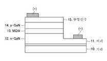
도 3은 본 발명의 일 실시예에 따른 발광 소자의 단면도이다.3 is a cross-sectional view of a light emitting device according to an embodiment of the present invention.
도 3에 도시된 발광 소자는 GaN 계 발광 다이오드(LED)를 구조를 예시로서 설명하고 있다. 발광 소자는 기판(10), 버퍼층(11), n형 반도체층(12), 다중 양자 우물층(MQW)(13), p형 반도체층(14), 투명 전극층(15)를 포함한다.The light emitting device shown in FIG. 3 illustrates a GaN-based light emitting diode (LED) as an example. The light emitting device includes a substrate 10, a buffer layer 11, an n-type semiconductor layer 12, a multi-quantum well layer (MQW) 13, a p-type semiconductor layer 14, and a transparent electrode layer 15.
여기서, 활성화층인 다중 양자 우물층(MQW)(13)는 InGaN로 형성될 수 있다. 여기서, n형 반도체층(12), 다중 양자 우물증(MQW)(13), p형 반도체층(14)는 중성 입자빔을 형성될 수 있음은 이미 상세히 설명하였다.Here, the multi-quantum well layer (MQW) 13, which is an activation layer, may be formed of InGaN. Here, the n-type semiconductor layer 12, the multiple quantum well (MQW) 13, the p-type semiconductor layer 14 has already been described in detail that can form a neutral particle beam.
도 4는 발광 소자의 제조 공정에 있어서 중성빔 에피 공정과 MOCVD 공정을 비교한 도면이다.4 is a view comparing the neutral beam epi process and the MOCVD process in the manufacturing process of the light emitting device.
도 4의 (a)에 도시된 MOCVD 공정을 살펴보면, 기판이 고온에서 세정된 후 저온에서 버퍼층(11)이 형성된다. 그 후 영역 A에서 1000~1100℃ 상태에서 n형 반도체층(12)가 형성된다. 이후, 영역 B에서 700~800℃ 상태에서 MQW층(13)이 형성된다. 그리고 다시 온도가 상승하여 영역 C에서 900~1000℃ 상태에서 p형 반도체층(14)가 형성될수 있다. Referring to the MOCVD process illustrated in FIG. 4A, after the substrate is cleaned at a high temperature, the buffer layer 11 is formed at a low temperature. Thereafter, the n-type semiconductor layer 12 is formed in the region A in a state of 1000 to 1100 ° C. Thereafter, in the region B, the
여기서, 주의할 점은 p형 반도체층 (14) 형성을 위한 영역 C에서는 p형 원소의 도핑 효율이 n형 원소의 도핑 효율에 비해 매우 낮다는 것이다. 더욱 상세하게, p형 원소 (예를 들어, Mg+)의 도핑 효율은 순수하게 온도에 의존하기 때문에 때문에 고열의 에너지를 제공하여야 하지만, 반면 기판 전체를 너 고온으로 가열하는 경우에는 p형 원소인 Mg+가 n형 반도체층(12) 이나 다중 양자 우물증(MQW)(13)으로 확산되어 발광 소자 전체의 품질을 떨어뜨리게 되는 문제점이 있다.Note that the doping efficiency of the p-type element in the region C for forming the p-type semiconductor layer 14 is very low compared to the doping efficiency of the n-type element. More specifically, the doping efficiency of the p-type element (eg, Mg +) is purely temperature dependent and therefore must provide high heat energy, whereas Mg +, the p-type element, is heated when you heat the entire substrate to high temperatures. Is diffused into the n-type semiconductor layer 12 or the multiple quantum well (MQW) 13, thereby lowering the quality of the entire light emitting device.
결국, MOCVD 공정에 있어서, p형 반도체층(14)를 형성하기 위해 저온에서 처리하면 p형 원소의 도핑 효율이 떨어져 상기 p형 원소가 결정에 참여하지 못하게 되어 전기 전도도를 떨어뜨리는 문제점이 존재한다. 반대로 고온에서 처리하면, p형 원소의 확산으로 인해 발광 소자 전체의 품질을 떨어뜨리는 문제점이 존재한다.As a result, in the MOCVD process, if the low-temperature treatment is performed to form the p-type semiconductor layer 14, there is a problem that the doping efficiency of the p-type element is lowered so that the p-type element does not participate in the crystal, thereby lowering the electrical conductivity. . On the contrary, when processing at high temperature, there is a problem that the quality of the entire light emitting device due to the diffusion of the p-type element.
반면, 도 5의 (b)에서와 같이 중성빔 에피 공정을 사용하는 경우에는 600 ℃수준의 저온에서의 도핑이 가능하므로, 기판의 손상을 방지하고 p형 원소의 확산을 방지할 수 있는 장점이 있다.On the other hand, when the neutral beam epi process is used as shown in FIG. 5 (b), doping at a low temperature of 600 ° C. is possible, thereby preventing damage to the substrate and preventing diffusion of p-type elements. have.
한편, 종래의 MOCVD 공정의 경우에는 중성 입자빔을 이용한 에피 공정보다는 제조 장치 가격이 저렴하고 처리 시간을 단축할 수 있는 장점이 있다.On the other hand, in the case of the conventional MOCVD process, there is an advantage that the manufacturing apparatus price is cheaper and the processing time can be shorter than the epi process using the neutral particle beam.
도 5는 본 발명의 다른 실시예에 따른 발광 소자 제조 방법을 도시한 흐름도이다.5 is a flowchart illustrating a method of manufacturing a light emitting device according to another embodiment of the present invention.
단계(S100), (S110)에서는 기판을 세정하고 버퍼층을 형성한다. 본 단계의 구체적인 공정 처리 방법은 종래의 GaN 계 LED 제조에 사용되었던 방법이 채용될수 있다.In steps S100 and S110, the substrate is cleaned and a buffer layer is formed. As a specific process treatment method of this step, the method used in the conventional GaN-based LED manufacturing can be adopted.
단계(S120)에서는 MOCVD 공정을 이용하여 n형 반도체 층을 형성한다. 여여기서, n형 원소로서는 Si가 이용될 수 있다. n형 반도체층은 p형 반도체층과 비교하여 도핑 효율이 높기 때문에 MOCVD 기술을 채택하는 경우, 빠른 처리 속도로 효율적으로 n형 원소를 도핑할 수 있다.In step S120, an n-type semiconductor layer is formed using a MOCVD process. Here, Si may be used as the n-type element. Since the n-type semiconductor layer has a higher doping efficiency than the p-type semiconductor layer, when the MOCVD technique is adopted, the n-type element can be efficiently doped at a high processing speed.
이후, 단계(S130)에서는 중성 입자빔 에피 공정을 이용하여 MQW층을 형성한다. 상기 MQW 층은 InGaN로 형성될 수 있다.Thereafter, in step S130 to form a MQW layer using a neutral particle beam epi process. The MQW layer may be formed of InGaN.
단계(S140)에서는 p형 반도체 층이 중성 입자빔 에피 공정으로 형성된다. p형 반도체 층의 p형 원소로서는 Mg+가 사용될 수 있다. 여기서, p형 원소는 n형 원소에 비해 도핑 효율이 많이 떨어진다. 또한, 고온에서는 다른 층으로 확산될 우려를 가지고 있다. 그러나, 단계(S140)에서는 p형 반도체층을 형성함에 있어, 저온에서 처리 가능한 중성 입자빔 에피 공정을 채택함으로써, 도핑 효율과 발광 소자의 품질 저하를 방지한다.In step S140, the p-type semiconductor layer is formed by a neutral particle beam epitaxial process. Mg + may be used as the p-type element of the p-type semiconductor layer. Here, the p-type element is much lower in doping efficiency than the n-type element. In addition, there is a fear of diffusion to other layers at high temperatures. However, in the step (S140) to form a p-type semiconductor layer, by adopting a neutral particle beam epi process that can be processed at a low temperature, the doping efficiency and the quality of the light emitting device is prevented.
단계(S150)에서는 p형 반도체층 위에 투명 전극을 형성한다.In step S150, a transparent electrode is formed on the p-type semiconductor layer.
도 5에 도시된 본 발명의 실시예에서 단계 (S120, S130, S140)은 각각 다른 챔버에서 처리될 수 있다. 예를 들어, 피처리 기판은 중앙의 로봇에 의해 최초로 MOCVD를 이용하여 n형 원소를 도핑하는 챔버로 기판을 투입하여 n형 반도체 층을 형성하고, 중성 입자빔을 이용하여 MQW층을 형성하는 챔버에서 MQW층을 형성하고, 다음 중성 입자빔을 이용하여 p형 원소를 도핑하는 챔버로 기판을 투입하여 p형 반도체층을 형성할 수 있다.In the embodiment of the present invention shown in FIG. 5, steps S120, S130, and S140 may be processed in different chambers, respectively. For example, the substrate to be processed is a chamber in which a substrate is first introduced into a chamber doping n-type elements by MOCVD using a central robot to form an n-type semiconductor layer, and a MQW layer is formed using a neutral particle beam. Forming an MQW layer in the, and then the substrate can be introduced into a chamber for doping the p-type element using a neutral particle beam to form a p-type semiconductor layer.
여기서, 중성 입자빔을 이용하는 챔버에서 처리되는 구체적인 예시는 본 발명의 명세서에서 이미 충분히 설명하였다.Here, specific examples of processing in a chamber using a neutral particle beam have already been fully described in the specification of the present invention.
이러한 구성에 의하여, 도핑 효율이 좋은 n형 반도체층 형성은 공정 처리 속도가 빠른 MOCVD를 채용하고, 도핑 효율이 상대적으로 좋지 않은 p형 반도체층 형성은 중성 입자빔을 이용함으로써, 전체적인 발광소자의 품질과 제조 효율성을 향상시킬 수 있다.With this configuration, the n-type semiconductor layer formation with good doping efficiency adopts MOCVD with high process processing speed, and the p-type semiconductor layer formation with relatively low doping efficiency uses neutral particle beam, so that the quality of the overall light emitting device is improved. And improve manufacturing efficiency.
본 발명의 권리는 위에서 설명된 실시예에 한정되지 않고 청구범위에 기재된 바에 의해 정의되며, 본 발명의 분야에서 통상의 지식을 가진 자가 청구범위에 기재된 권리범위 내에서 다양한 변형과 개작을 할 수 있음은 자명하다.The rights of the present invention are not limited to the embodiments described above, but are defined by the claims, and various changes and modifications can be made by those of ordinary skill in the art within the scope of the claims. Is self explanatory.
1: 중성입자 빔 발생원 2: 중성입자 빔
3: 고체원소 발생원 4: 3 족 원소
5: 기판 6: 기판 탑재대
7: 공정 챔버 8: 도핑용 고체원소 발생원1: Neutral beam source 2: Neutral beam
3: solid element generator 4: group 3 element
5: Substrate 6: Board Mount
7: Process Chamber 8: Doping Solid Element Source
Claims (14)
Translated fromKorean상기 중성입자 빔이 상기 기판에 닿기 직전 또는 직후에 3 족 고체원소를 방출하는 단계;를 포함하여,
상기 중성입자 빔과 상기 3 족 고체원소가 상기 기판상에 질화물 반도체 단결정 박막으로 증착되는 것을 특징으로 하는 질화물 반도체 단결정 박막 형성 방법.
Emitting a neutral particle beam comprising a nitrogen (N) atom and an inert element; And
Emitting a group 3 solid element immediately before or immediately after the neutral particle beam contacts the substrate;
And the neutral particle beam and the group 3 solid element are deposited on the substrate as a nitride semiconductor single crystal thin film.
상기 질화물 반도체 단결정 박막의 형성 방법에 의해 형성되고 있는 질화물 반도체 단결정 박막에, 도핑하고자 하는 고체원소를, 전구체 분사 가스 없이 직접적으로 제공하도록 방출하는 단계를, 상기 3 족 고체 원소 방출 단계와 동시에 더 포함하는 것을 특징으로 하는 질화물 반도체 단결정 박막 형성 방법.
The method of claim 1,
And simultaneously discharging the nitride semiconductor single crystal thin film formed by the method of forming the nitride semiconductor single crystal thin film so as to directly provide a solid element to be doped without a precursor injection gas, simultaneously with the Group 3 solid element discharge step. A method of forming a nitride semiconductor single crystal thin film, characterized in that.
상기 중성입자 빔의 방출과 동시에 3 족 고체원소를 방출하고,
형성되는 질화물 반도체 단결정 박막에 도핑하고자 하는 고체원소 또한 동시에 방출하는 것을 특징으로 하는 질화물 반도체 단결정 박막 형성 방법.
While emitting a beam of neutral particles containing nitrogen (N) atoms and inert elements
Emits Group 3 solid elements simultaneously with the emission of the neutral particle beam,
A method of forming a nitride semiconductor single crystal thin film, characterized in that simultaneously emitting a solid element to be doped into the nitride semiconductor single crystal thin film to be formed.
상기 불활성 원소는 Ar, He, Ne, Kr, Xe 중 하나이거나, 둘 이상의 원소를 혼합한 것으로 구성되는 것을 특징으로 하는 질화물 반도체 단결정 박막 형성 방법.
The method of claim 2 or 3,
The inert element is one of Ar, He, Ne, Kr, Xe, or a method of forming a nitride semiconductor single crystal thin film, characterized in that consisting of a mixture of two or more elements.
상기 3 족 고체원소는 Al, Ga, In 중 하나이거나, 둘 이상의 원소를 혼합하여 구성되는 것을 특징으로 하는 질화물 반도체 단결정 박막 형성 방법.
The method of claim 4, wherein
The group 3 solid element is one of Al, Ga, In, or a nitride semiconductor single crystal thin film formation method characterized in that it is composed by mixing two or more elements.
상기 기판의 온도를 200 내지 800 ℃ 로 유지하는 것을 특징으로 하는 질화물 반도체 단결정 박막 형성 방법.
The method of claim 5,
The temperature of the substrate is maintained at 200 to 800 ° C characterized in that the nitride semiconductor single crystal thin film forming method.
상기 중성입자 빔의 운동에너지를 1 내지 100 eV로 하는 것을 특징으로 하는 질화물 반도체 단결정 박막 형성 방법.
The method according to claim 6,
The method of forming a nitride semiconductor single crystal thin film, characterized in that the kinetic energy of the neutral particle beam is 1 to 100 eV.
상기 3 족 고체원소의 방출 단계는 출사와 정지를 주기적으로 반복하는 모듈레이션(modulation) 모드로 동작하는 것을 특징으로 하는 질화물 반도체 단결정 박막 형성 방법.
The method of claim 7, wherein
And discharging the group 3 solid element in a modulation mode to periodically emit and stop.
출사 시간


을 만족하는 것을 특징으로 하는 질화물 반도체 단결정 박막 형성 방법.
여기서


9. The method of claim 8,
Exit time
The method for forming a nitride semiconductor single crystal thin film, characterized in that the satisfactory.
here
상기 3족 고체원소의 방출과 도핑하고자 하는 고체원소의 방출은 출사 및 정지를 동기화하여 주기적으로 반복하는 것을 특징으로 하는 질화물 반도체 단결정 박막 형성 방법.
10. The method of claim 9,
The method of forming a nitride semiconductor single crystal thin film, characterized in that the emission of the Group 3 solid element and the emission of the solid element to be doped is repeated periodically in synchronization with the emission and stop.
상기 3족 고체원소의 방출과 도핑하고자 하는 고체원소의 방출은 출사 및 정지를 서로 엇갈리게 하여 주기적으로 반복하는 것을 특징으로 하는 질화물 반도체 단결정 박막 형성 방법.
10. The method of claim 9,
The method of forming a nitride semiconductor single crystal thin film, characterized in that the emission of the Group 3 solid element and the emission of the solid element to be doped are periodically repeated by staggering the emission and stop.
상기 중성입자 빔 발생장치의 동작과 함께 3 족 고체원소를 기판상으로 분사하는 고체원소 발생장치; 및
형성되는 질화물 반도체 단결정 박막에 도핑 원소를 전구체 분사 가스 없이 직접적으로 제공하기 위한 도핑용 고체원소 발생장치;를 포함하는 것을 특징으로 하는 질화물 반도체 단결정 박막 형성 장치.
A neutral particle beam generating device generating nitrogen (N) and an inert element as neutral particles and exiting the substrate;
A solid element generator for injecting group III solid elements onto a substrate together with the operation of the neutral particle beam generator; And
And a doping solid element generator for directly providing a doping element to a nitride semiconductor single crystal thin film to be formed without a precursor injection gas.
유기금속화학증착(MOCVD)법을 이용하여 n형 원소를 도핑하여 n형 반도체 층을 형성하는 단계,
중성 입자빔을 이용하여 활성층을 형성하는 단계 및
중성 입자빔 및 p형 원소를 도핑하여 p형 반도체 층을 형성하는 단계를 형성하는 단계를 포함하는 발광 소자 제조 방법.
In the light emitting device manufacturing method,
Forming an n-type semiconductor layer by doping the n-type element using an organometallic chemical vapor deposition (MOCVD) method,
Forming an active layer using a neutral particle beam, and
And forming a p-type semiconductor layer by doping the neutral particle beam and the p-type element.
유기금속화학증착(MOCVD)법을 이용하여 n형 원소를 도핑하여 n형 반도체 층을 형성하는 제 1 챔버와,
중성 입자빔 및 p형 원소를 도핑하여 p형 반도체 층을 형성하는 단계를 형성하는 단계를 포함하는 제 2 챔버를 포함하고,
상기 제 2 챔버는, 중성입자 빔 발생장치와, 상기 중성입자 빔 발생장치의 동작과 함께 3 족 고체원소를 기판상으로 분사하는 고체원소 발생장치와, 형성되는 질화물 반도체 단결정 박막에 p형 도핑 원소를 전구체 분사 가스 없이 직접적으로 제공하기 위한 p형 도핑용 고체원소 발생장치를 포함하는 것인 발광 소자 제조 장치.In the light emitting device manufacturing apparatus,
A first chamber in which an n-type semiconductor layer is formed by doping an n-type element using organometallic chemical vapor deposition (MOCVD);
A second chamber comprising forming a p-type semiconductor layer by doping the neutral particle beam and the p-type element,
The second chamber includes a neutral particle beam generator, a solid element generator for injecting Group 3 solid elements onto a substrate together with the operation of the neutral particle beam generator, and a p-type doping element in the nitride semiconductor single crystal thin film formed. Light emitting device manufacturing apparatus comprising a p-type doping solid element generator for providing directly without a precursor injection gas.
Priority Applications (6)
| Application Number | Priority Date | Filing Date | Title |
|---|---|---|---|
| KR1020110026029AKR20120108324A (en) | 2011-03-23 | 2011-03-23 | Method and apparatus for manufacturing light emit device using hyperthermal neutral beam |
| PCT/KR2011/003943WO2012128420A1 (en) | 2011-03-23 | 2011-05-30 | Apparatus and method for manufacturing a light-emitting device using a neutral particle beam |
| CN201180069512.8ACN103460341B (en) | 2011-03-23 | 2011-05-30 | Light-emitting element manufacturing method and device using neutral particle beam |
| JP2014500976AJP5729893B2 (en) | 2011-03-23 | 2011-05-30 | Method and apparatus for manufacturing light emitting device using neutral particle beam |
| US14/006,937US9275859B2 (en) | 2011-03-23 | 2011-05-30 | Apparatus and method for manufacturing a light-emitting device using a neutral particle beam |
| EP11861350.4AEP2690651A4 (en) | 2011-03-23 | 2011-05-30 | APPARATUS AND METHOD FOR MANUFACTURING A LIGHT EMITTING DEVICE USING A NEUTRAL PARTICLE BEAM |
Applications Claiming Priority (1)
| Application Number | Priority Date | Filing Date | Title |
|---|---|---|---|
| KR1020110026029AKR20120108324A (en) | 2011-03-23 | 2011-03-23 | Method and apparatus for manufacturing light emit device using hyperthermal neutral beam |
Related Child Applications (1)
| Application Number | Title | Priority Date | Filing Date |
|---|---|---|---|
| KR1020160008001ADivisionKR20160017654A (en) | 2016-01-22 | 2016-01-22 | Method and apparatus for manufacturing light emit device using hyperthermal neutral beam |
Publications (1)
| Publication Number | Publication Date |
|---|---|
| KR20120108324Atrue KR20120108324A (en) | 2012-10-05 |
Family
ID=46879542
Family Applications (1)
| Application Number | Title | Priority Date | Filing Date |
|---|---|---|---|
| KR1020110026029ACeasedKR20120108324A (en) | 2011-03-23 | 2011-03-23 | Method and apparatus for manufacturing light emit device using hyperthermal neutral beam |
Country Status (6)
| Country | Link |
|---|---|
| US (1) | US9275859B2 (en) |
| EP (1) | EP2690651A4 (en) |
| JP (1) | JP5729893B2 (en) |
| KR (1) | KR20120108324A (en) |
| CN (1) | CN103460341B (en) |
| WO (1) | WO2012128420A1 (en) |
Families Citing this family (1)
| Publication number | Priority date | Publication date | Assignee | Title |
|---|---|---|---|---|
| GB2530982B (en)* | 2014-09-30 | 2018-10-24 | M Solv Ltd | Bernoulli process head |
Family Cites Families (21)
| Publication number | Priority date | Publication date | Assignee | Title |
|---|---|---|---|---|
| JP3075581B2 (en)* | 1991-05-23 | 2000-08-14 | 松下電器産業株式会社 | Apparatus for growing nitride-based compound semiconductor films |
| EP0652308B1 (en) | 1993-10-14 | 2002-03-27 | Neuralsystems Corporation | Method of and apparatus for forming single-crystalline thin film |
| JPH07291791A (en)* | 1994-04-15 | 1995-11-07 | Nippon Steel Corp | Molecular beam epitaxy system |
| JPH10290048A (en)* | 1997-04-15 | 1998-10-27 | Hitachi Ltd | Method of forming compound semiconductor and semiconductor device |
| JP4458870B2 (en)* | 2004-02-10 | 2010-04-28 | 日本碍子株式会社 | Fluorescent light emitting device, fluorescent light emitting element, and phosphor |
| US20050230350A1 (en)* | 2004-02-26 | 2005-10-20 | Applied Materials, Inc. | In-situ dry clean chamber for front end of line fabrication |
| KR100669828B1 (en)* | 2005-03-22 | 2007-01-16 | 성균관대학교산학협력단 | Atomic Layer Deposition Apparatus Using Neutral Beam and Atomic Layer Deposition Method Using Apparatus |
| GB0509328D0 (en)* | 2005-05-09 | 2005-06-15 | Univ Nottingham | A bulk, free-standing cubic III-N substrate and a method for forming same |
| US7393762B2 (en)* | 2005-11-21 | 2008-07-01 | Los Alamos National Secruity, Llc | Charge-free low-temperature method of forming thin film-based nanoscale materials and structures on a substrate |
| US7810743B2 (en) | 2006-01-23 | 2010-10-12 | Kimberly-Clark Worldwide, Inc. | Ultrasonic liquid delivery device |
| KR100754370B1 (en)* | 2006-06-29 | 2007-09-03 | 한국기초과학지원연구원 | Neutral Particle Beam Generator with Improved Neutral Particle Flux |
| JP5194656B2 (en)* | 2007-09-06 | 2013-05-08 | 住友電気工業株式会社 | Particle beam supply apparatus and method for growing III-V compound semiconductor |
| JP5128907B2 (en)* | 2007-11-02 | 2013-01-23 | 学校法人同志社 | Activity controlled nitrogen compound MBE film forming method and apparatus |
| JP2009295692A (en)* | 2008-06-03 | 2009-12-17 | Sumitomo Electric Ind Ltd | Method for manufacturing of semiconductor laser element |
| KR101111962B1 (en)* | 2008-10-24 | 2012-06-12 | 한국기초과학지원연구원 | Apparatus and method for forming nitridation film of using the nitrogen atom beam |
| US8427590B2 (en)* | 2009-05-29 | 2013-04-23 | Soraa, Inc. | Laser based display method and system |
| KR101092906B1 (en)* | 2009-06-11 | 2011-12-12 | 한국기초과학지원연구원 | Neutral particle beam generating apparatus and method with increased neutral particle flux and transport |
| EP2275591B1 (en)* | 2009-07-10 | 2014-03-19 | Imec | Method for manufacturing a mono-crystalline layer of germanium or aluminium on a substrate |
| KR101121055B1 (en)* | 2009-08-13 | 2012-03-15 | 한국기초과학지원연구원 | Apparatus and method for forming nitridation film of using the nitrogen atom beam a energy controllable |
| KR101038767B1 (en)* | 2009-09-24 | 2011-06-03 | 한국기초과학지원연구원 | Nitride Semiconductor Single Crystal Thin Film Forming Apparatus and Method |
| US8409895B2 (en)* | 2010-12-16 | 2013-04-02 | Applied Materials, Inc. | Gallium nitride-based LED fabrication with PVD-formed aluminum nitride buffer layer |
- 2011
- 2011-03-23KRKR1020110026029Apatent/KR20120108324A/ennot_activeCeased
- 2011-05-30CNCN201180069512.8Apatent/CN103460341B/enactiveActive
- 2011-05-30EPEP11861350.4Apatent/EP2690651A4/ennot_activeWithdrawn
- 2011-05-30WOPCT/KR2011/003943patent/WO2012128420A1/enactiveApplication Filing
- 2011-05-30JPJP2014500976Apatent/JP5729893B2/enactiveActive
- 2011-05-30USUS14/006,937patent/US9275859B2/enactiveActive
Also Published As
| Publication number | Publication date |
|---|---|
| US9275859B2 (en) | 2016-03-01 |
| US20140017827A1 (en) | 2014-01-16 |
| CN103460341A (en) | 2013-12-18 |
| CN103460341B (en) | 2016-03-02 |
| JP5729893B2 (en) | 2015-06-03 |
| EP2690651A4 (en) | 2014-12-31 |
| JP2014510414A (en) | 2014-04-24 |
| EP2690651A1 (en) | 2014-01-29 |
| WO2012128420A1 (en) | 2012-09-27 |
Similar Documents
| Publication | Publication Date | Title |
|---|---|---|
| CN100356590C (en) | Light emitting element and manufacturing method thereof | |
| US8735290B2 (en) | Amorphous group III-V semiconductor material and preparation thereof | |
| JP5072397B2 (en) | Gallium nitride compound semiconductor light emitting device and method of manufacturing the same | |
| JP2000286449A (en) | Iii nitride compound semiconductor device and its manufacture | |
| WO2007029711A1 (en) | Semiconductor light-emitting device and method for manufacturing same | |
| US8202761B2 (en) | Manufacturing method of metal oxide nanostructure and electronic element having the same | |
| US9209361B2 (en) | Nitride semiconductor light-emitting element | |
| US8222055B2 (en) | Silicon nitride layer for light emitting device, light emitting device using the same, and method of forming silicon nitride layer for light emitting device | |
| JP5196655B2 (en) | Method for producing zinc oxide semiconductor crystal | |
| JP2001351925A (en) | METHOD FOR MANUFACTURING p-TYPE NITRIDE-BASED III-V COMPOUND SEMICONDUCTOR AND METHOD FOR MANUFACTURING SEMICONDUCTOR ELEMENT | |
| KR101038767B1 (en) | Nitride Semiconductor Single Crystal Thin Film Forming Apparatus and Method | |
| US6881601B2 (en) | Nitride compound semiconductor, nitride compound semiconductor light emitting device and method of manufacturing the same | |
| TWI243523B (en) | MBE growth of semiconductor laser diode | |
| US8772150B2 (en) | Method of forming p-type ZnO film | |
| US20140235005A1 (en) | Method of producing p-type nitride semiconductor and method of manufacturing nitride semiconductor light emitting device therewith | |
| JP2012204540A (en) | Semiconductor device and method of manufacturing the same | |
| KR20120108324A (en) | Method and apparatus for manufacturing light emit device using hyperthermal neutral beam | |
| KR20160017654A (en) | Method and apparatus for manufacturing light emit device using hyperthermal neutral beam | |
| US8653501B2 (en) | Emitting device and manufacturing method therefor | |
| JP2011096902A (en) | ZuO-BASED COMPOUND SEMICONDUCTOR ELEMENT AND MANUFACTURING METHOD OF THE SAME | |
| JP3331591B2 (en) | Light-emitting material, method of manufacturing the same, and light-emitting element using the same | |
| JP2001015808A (en) | Nitrogen compound semiconductor light emitting device and method of manufacturing the same | |
| JP2004128189A (en) | Method for manufacturing gallium nitride system compound semiconductor | |
| WO2019224966A1 (en) | Method for producing group iii-v compound semiconductor device | |
| KR20150133628A (en) | Light emitting device and method of fabricating the same |
Legal Events
| Date | Code | Title | Description |
|---|---|---|---|
| PA0109 | Patent application | St.27 status event code:A-0-1-A10-A12-nap-PA0109 | |
| P11-X000 | Amendment of application requested | St.27 status event code:A-2-2-P10-P11-nap-X000 | |
| P13-X000 | Application amended | St.27 status event code:A-2-2-P10-P13-nap-X000 | |
| R18-X000 | Changes to party contact information recorded | St.27 status event code:A-3-3-R10-R18-oth-X000 | |
| PN2301 | Change of applicant | St.27 status event code:A-3-3-R10-R13-asn-PN2301 St.27 status event code:A-3-3-R10-R11-asn-PN2301 | |
| PG1501 | Laying open of application | St.27 status event code:A-1-1-Q10-Q12-nap-PG1501 | |
| PN2301 | Change of applicant | St.27 status event code:A-3-3-R10-R13-asn-PN2301 St.27 status event code:A-3-3-R10-R11-asn-PN2301 | |
| A201 | Request for examination | ||
| PA0201 | Request for examination | St.27 status event code:A-1-2-D10-D11-exm-PA0201 | |
| E902 | Notification of reason for refusal | ||
| PE0902 | Notice of grounds for rejection | St.27 status event code:A-1-2-D10-D21-exm-PE0902 | |
| T11-X000 | Administrative time limit extension requested | St.27 status event code:U-3-3-T10-T11-oth-X000 | |
| T11-X000 | Administrative time limit extension requested | St.27 status event code:U-3-3-T10-T11-oth-X000 | |
| T11-X000 | Administrative time limit extension requested | St.27 status event code:U-3-3-T10-T11-oth-X000 | |
| AMND | Amendment | ||
| E13-X000 | Pre-grant limitation requested | St.27 status event code:A-2-3-E10-E13-lim-X000 | |
| P11-X000 | Amendment of application requested | St.27 status event code:A-2-2-P10-P11-nap-X000 | |
| P13-X000 | Application amended | St.27 status event code:A-2-2-P10-P13-nap-X000 | |
| E601 | Decision to refuse application | ||
| PE0601 | Decision on rejection of patent | St.27 status event code:N-2-6-B10-B15-exm-PE0601 | |
| T11-X000 | Administrative time limit extension requested | St.27 status event code:U-3-3-T10-T11-oth-X000 | |
| AMND | Amendment | ||
| P11-X000 | Amendment of application requested | St.27 status event code:A-2-2-P10-P11-nap-X000 | |
| R17-X000 | Change to representative recorded | St.27 status event code:A-3-3-R10-R17-oth-X000 | |
| P11-X000 | Amendment of application requested | St.27 status event code:A-2-2-P10-P11-nap-X000 | |
| P13-X000 | Application amended | St.27 status event code:A-2-2-P10-P13-nap-X000 | |
| E801 | Decision on dismissal of amendment | ||
| PE0601 | Decision on rejection of patent | St.27 status event code:N-2-6-B10-B15-exm-PE0601 | |
| PE0801 | Dismissal of amendment | St.27 status event code:A-2-2-P10-P12-nap-PE0801 | |
| A107 | Divisional application of patent | ||
| PA0107 | Divisional application | St.27 status event code:A-0-1-A10-A18-div-PA0107 St.27 status event code:A-0-1-A10-A16-div-PA0107 | |
| R18-X000 | Changes to party contact information recorded | St.27 status event code:A-3-3-R10-R18-oth-X000 | |
| P22-X000 | Classification modified | St.27 status event code:A-2-2-P10-P22-nap-X000 |