KR20120104096A - Liquid crystal display device - Google Patents
Liquid crystal display deviceDownload PDFInfo
- Publication number
- KR20120104096A KR20120104096AKR1020120023859AKR20120023859AKR20120104096AKR 20120104096 AKR20120104096 AKR 20120104096AKR 1020120023859 AKR1020120023859 AKR 1020120023859AKR 20120023859 AKR20120023859 AKR 20120023859AKR 20120104096 AKR20120104096 AKR 20120104096A
- Authority
- KR
- South Korea
- Prior art keywords
- insulating film
- electrode
- wiring
- liquid crystal
- pixel
- Prior art date
- Legal status (The legal status is an assumption and is not a legal conclusion. Google has not performed a legal analysis and makes no representation as to the accuracy of the status listed.)
- Granted
Links
- 239000004973liquid crystal related substanceSubstances0.000titleclaimsabstractdescription238
- 239000004065semiconductorSubstances0.000claimsdescription129
- 238000000034methodMethods0.000claimsdescription77
- 239000000758substrateSubstances0.000claimsdescription56
- 230000005684electric fieldEffects0.000abstractdescription39
- 238000004519manufacturing processMethods0.000abstractdescription26
- 229910052751metalInorganic materials0.000abstractdescription24
- 239000002184metalSubstances0.000abstractdescription23
- 230000003071parasitic effectEffects0.000abstractdescription15
- 239000010408filmSubstances0.000description448
- 239000010410layerSubstances0.000description359
- 239000000463materialSubstances0.000description59
- 239000012071phaseSubstances0.000description52
- 230000006870functionEffects0.000description28
- 230000008569processEffects0.000description23
- 238000005530etchingMethods0.000description22
- 229910052719titaniumInorganic materials0.000description19
- 239000010936titaniumSubstances0.000description19
- IJGRMHOSHXDMSA-UHFFFAOYSA-NAtomic nitrogenChemical compoundN#NIJGRMHOSHXDMSA-UHFFFAOYSA-N0.000description18
- 239000012535impuritySubstances0.000description18
- 238000002834transmittanceMethods0.000description18
- RTAQQCXQSZGOHL-UHFFFAOYSA-NTitaniumChemical compound[Ti]RTAQQCXQSZGOHL-UHFFFAOYSA-N0.000description17
- 239000007789gasSubstances0.000description16
- 238000012545processingMethods0.000description16
- 229910052782aluminiumInorganic materials0.000description14
- XAGFODPZIPBFFR-UHFFFAOYSA-NaluminiumChemical compound[Al]XAGFODPZIPBFFR-UHFFFAOYSA-N0.000description12
- 238000001020plasma etchingMethods0.000description12
- 239000011347resinSubstances0.000description12
- 229920005989resinPolymers0.000description12
- 229910052581Si3N4Inorganic materials0.000description11
- 229910007541Zn OInorganic materials0.000description11
- HQVNEWCFYHHQES-UHFFFAOYSA-Nsilicon nitrideChemical compoundN12[Si]34N5[Si]62N3[Si]51N64HQVNEWCFYHHQES-UHFFFAOYSA-N0.000description11
- 229910045601alloyInorganic materials0.000description10
- 239000000956alloySubstances0.000description10
- QVGXLLKOCUKJST-UHFFFAOYSA-Natomic oxygenChemical compound[O]QVGXLLKOCUKJST-UHFFFAOYSA-N0.000description10
- 238000001312dry etchingMethods0.000description10
- 239000001301oxygenSubstances0.000description10
- 229910052760oxygenInorganic materials0.000description10
- 239000003990capacitorSubstances0.000description9
- 229910021424microcrystalline siliconInorganic materials0.000description9
- 229910052757nitrogenInorganic materials0.000description9
- XUIMIQQOPSSXEZ-UHFFFAOYSA-NSiliconChemical compound[Si]XUIMIQQOPSSXEZ-UHFFFAOYSA-N0.000description8
- 239000011159matrix materialSubstances0.000description8
- 229910021420polycrystalline siliconInorganic materials0.000description8
- 229910052710siliconInorganic materials0.000description8
- 239000010703siliconSubstances0.000description8
- VYPSYNLAJGMNEJ-UHFFFAOYSA-Nsilicon dioxideInorganic materialsO=[Si]=OVYPSYNLAJGMNEJ-UHFFFAOYSA-N0.000description8
- 229910021417amorphous siliconInorganic materials0.000description7
- 229920000642polymerPolymers0.000description7
- 229920005591polysiliconPolymers0.000description7
- 230000004044responseEffects0.000description7
- 229910052814silicon oxideInorganic materials0.000description7
- 230000006641stabilisationEffects0.000description7
- 238000011105stabilizationMethods0.000description7
- ZAMOUSCENKQFHK-UHFFFAOYSA-NChlorine atomChemical compound[Cl]ZAMOUSCENKQFHK-UHFFFAOYSA-N0.000description6
- OAICVXFJPJFONN-UHFFFAOYSA-NPhosphorusChemical compound[P]OAICVXFJPJFONN-UHFFFAOYSA-N0.000description6
- 239000000460chlorineSubstances0.000description6
- 229910052801chlorineInorganic materials0.000description6
- 239000013078crystalSubstances0.000description6
- 229910052733galliumInorganic materials0.000description6
- 239000011521glassSubstances0.000description6
- 239000001257hydrogenSubstances0.000description6
- 229910052739hydrogenInorganic materials0.000description6
- 239000000203mixtureSubstances0.000description6
- 125000000962organic groupChemical group0.000description6
- 229910052698phosphorusInorganic materials0.000description6
- 239000011574phosphorusSubstances0.000description6
- 239000002356single layerSubstances0.000description6
- WFKWXMTUELFFGS-UHFFFAOYSA-NtungstenChemical compound[W]WFKWXMTUELFFGS-UHFFFAOYSA-N0.000description6
- 229910052721tungstenInorganic materials0.000description6
- 239000010937tungstenSubstances0.000description6
- UWCWUCKPEYNDNV-LBPRGKRZSA-N2,6-dimethyl-n-[[(2s)-pyrrolidin-2-yl]methyl]anilineChemical compoundCC1=CC=CC(C)=C1NC[C@H]1NCCC1UWCWUCKPEYNDNV-LBPRGKRZSA-N0.000description5
- 229910019092Mg-OInorganic materials0.000description5
- 229910019395Mg—OInorganic materials0.000description5
- BLRPTPMANUNPDV-UHFFFAOYSA-NSilaneChemical compound[SiH4]BLRPTPMANUNPDV-UHFFFAOYSA-N0.000description5
- 230000015572biosynthetic processEffects0.000description5
- 238000004891communicationMethods0.000description5
- 125000004435hydrogen atomChemical class[H]*0.000description5
- 238000002156mixingMethods0.000description5
- 238000000016photochemical curingMethods0.000description5
- 238000005268plasma chemical vapour depositionMethods0.000description5
- 238000004544sputter depositionMethods0.000description5
- 230000007704transitionEffects0.000description5
- FAQYAMRNWDIXMY-UHFFFAOYSA-NtrichloroboraneChemical compoundClB(Cl)ClFAQYAMRNWDIXMY-UHFFFAOYSA-N0.000description5
- WZJUBBHODHNQPW-UHFFFAOYSA-N2,4,6,8-tetramethyl-1,3,5,7,2$l^{3},4$l^{3},6$l^{3},8$l^{3}-tetraoxatetrasilocaneChemical compoundC[Si]1O[Si](C)O[Si](C)O[Si](C)O1WZJUBBHODHNQPW-UHFFFAOYSA-N0.000description4
- XKRFYHLGVUSROY-UHFFFAOYSA-NArgonChemical compound[Ar]XKRFYHLGVUSROY-UHFFFAOYSA-N0.000description4
- YCKRFDGAMUMZLT-UHFFFAOYSA-NFluorine atomChemical compound[F]YCKRFDGAMUMZLT-UHFFFAOYSA-N0.000description4
- 239000004990Smectic liquid crystalSubstances0.000description4
- BOTDANWDWHJENH-UHFFFAOYSA-NTetraethyl orthosilicateChemical compoundCCO[Si](OCC)(OCC)OCCBOTDANWDWHJENH-UHFFFAOYSA-N0.000description4
- 230000009471actionEffects0.000description4
- 238000006243chemical reactionMethods0.000description4
- 238000005229chemical vapour depositionMethods0.000description4
- 230000003098cholesteric effectEffects0.000description4
- 239000010949copperSubstances0.000description4
- 230000007547defectEffects0.000description4
- 238000010586diagramMethods0.000description4
- 229910052731fluorineInorganic materials0.000description4
- 239000011737fluorineSubstances0.000description4
- 229910052738indiumInorganic materials0.000description4
- 238000009616inductively coupled plasmaMethods0.000description4
- 238000003780insertionMethods0.000description4
- 230000037431insertionEffects0.000description4
- 239000007788liquidSubstances0.000description4
- 229910052750molybdenumInorganic materials0.000description4
- HMMGMWAXVFQUOA-UHFFFAOYSA-NoctamethylcyclotetrasiloxaneChemical compoundC[Si]1(C)O[Si](C)(C)O[Si](C)(C)O[Si](C)(C)O1HMMGMWAXVFQUOA-UHFFFAOYSA-N0.000description4
- 229910000077silaneInorganic materials0.000description4
- VZGDMQKNWNREIO-UHFFFAOYSA-NtetrachloromethaneChemical compoundClC(Cl)(Cl)ClVZGDMQKNWNREIO-UHFFFAOYSA-N0.000description4
- XLYOFNOQVPJJNP-UHFFFAOYSA-NwaterSubstancesOXLYOFNOQVPJJNP-UHFFFAOYSA-N0.000description4
- 239000004925Acrylic resinSubstances0.000description3
- 229920000178Acrylic resinPolymers0.000description3
- VYZAMTAEIAYCRO-UHFFFAOYSA-NChromiumChemical compound[Cr]VYZAMTAEIAYCRO-UHFFFAOYSA-N0.000description3
- RYGMFSIKBFXOCR-UHFFFAOYSA-NCopperChemical compound[Cu]RYGMFSIKBFXOCR-UHFFFAOYSA-N0.000description3
- ZOKXTWBITQBERF-UHFFFAOYSA-NMolybdenumChemical compound[Mo]ZOKXTWBITQBERF-UHFFFAOYSA-N0.000description3
- 230000008901benefitEffects0.000description3
- 239000005380borophosphosilicate glassSubstances0.000description3
- 230000008859changeEffects0.000description3
- 229910052804chromiumInorganic materials0.000description3
- 239000011651chromiumSubstances0.000description3
- 150000001875compoundsChemical class0.000description3
- 229910052802copperInorganic materials0.000description3
- KPUWHANPEXNPJT-UHFFFAOYSA-NdisiloxaneChemical class[SiH3]O[SiH3]KPUWHANPEXNPJT-UHFFFAOYSA-N0.000description3
- 230000001747exhibiting effectEffects0.000description3
- 239000005262ferroelectric liquid crystals (FLCs)Substances0.000description3
- 229910052735hafniumInorganic materials0.000description3
- 229910000449hafnium oxideInorganic materials0.000description3
- WIHZLLGSGQNAGK-UHFFFAOYSA-Nhafnium(4+);oxygen(2-)Chemical compound[O-2].[O-2].[Hf+4]WIHZLLGSGQNAGK-UHFFFAOYSA-N0.000description3
- 238000010438heat treatmentMethods0.000description3
- APFVFJFRJDLVQX-UHFFFAOYSA-Nindium atomChemical compound[In]APFVFJFRJDLVQX-UHFFFAOYSA-N0.000description3
- 239000003999initiatorSubstances0.000description3
- 239000011810insulating materialSubstances0.000description3
- 230000001678irradiating effectEffects0.000description3
- 238000002844meltingMethods0.000description3
- 230000008018meltingEffects0.000description3
- 229910044991metal oxideInorganic materials0.000description3
- 150000004706metal oxidesChemical group0.000description3
- 239000011733molybdenumSubstances0.000description3
- TWNQGVIAIRXVLR-UHFFFAOYSA-Noxo(oxoalumanyloxy)alumaneChemical compoundO=[Al]O[Al]=OTWNQGVIAIRXVLR-UHFFFAOYSA-N0.000description3
- BPUBBGLMJRNUCC-UHFFFAOYSA-Noxygen(2-);tantalum(5+)Chemical compound[O-2].[O-2].[O-2].[O-2].[O-2].[Ta+5].[Ta+5]BPUBBGLMJRNUCC-UHFFFAOYSA-N0.000description3
- 238000007639printingMethods0.000description3
- 238000004528spin coatingMethods0.000description3
- 239000000126substanceSubstances0.000description3
- 229910052715tantalumInorganic materials0.000description3
- GUVRBAGPIYLISA-UHFFFAOYSA-Ntantalum atomChemical compound[Ta]GUVRBAGPIYLISA-UHFFFAOYSA-N0.000description3
- 229910001936tantalum oxideInorganic materials0.000description3
- TXEYQDLBPFQVAA-UHFFFAOYSA-NtetrafluoromethaneChemical compoundFC(F)(F)FTXEYQDLBPFQVAA-UHFFFAOYSA-N0.000description3
- CZDYPVPMEAXLPK-UHFFFAOYSA-NtetramethylsilaneChemical compoundC[Si](C)(C)CCZDYPVPMEAXLPK-UHFFFAOYSA-N0.000description3
- 229910018516Al—OInorganic materials0.000description2
- BSYNRYMUTXBXSQ-UHFFFAOYSA-NAspirinChemical compoundCC(=O)OC1=CC=CC=C1C(O)=OBSYNRYMUTXBXSQ-UHFFFAOYSA-N0.000description2
- ZOXJGFHDIHLPTG-UHFFFAOYSA-NBoronChemical compound[B]ZOXJGFHDIHLPTG-UHFFFAOYSA-N0.000description2
- 229910014472Ca—OInorganic materials0.000description2
- GYHNNYVSQQEPJS-UHFFFAOYSA-NGalliumChemical compound[Ga]GYHNNYVSQQEPJS-UHFFFAOYSA-N0.000description2
- UFHFLCQGNIYNRP-UHFFFAOYSA-NHydrogenChemical compound[H][H]UFHFLCQGNIYNRP-UHFFFAOYSA-N0.000description2
- 229910003023Mg-AlInorganic materials0.000description2
- BPQQTUXANYXVAA-UHFFFAOYSA-NOrthosilicateChemical compound[O-][Si]([O-])([O-])[O-]BPQQTUXANYXVAA-UHFFFAOYSA-N0.000description2
- 239000004642PolyimideSubstances0.000description2
- 238000001237Raman spectrumMethods0.000description2
- 229910001069Ti alloyInorganic materials0.000description2
- GDFCWFBWQUEQIJ-UHFFFAOYSA-N[B].[P]Chemical compound[B].[P]GDFCWFBWQUEQIJ-UHFFFAOYSA-N0.000description2
- 238000010521absorption reactionMethods0.000description2
- 239000002253acidSubstances0.000description2
- 229910052786argonInorganic materials0.000description2
- 230000004888barrier functionEffects0.000description2
- 239000002585baseSubstances0.000description2
- 229910052796boronInorganic materials0.000description2
- 230000001413cellular effectEffects0.000description2
- 239000004020conductorSubstances0.000description2
- 230000008878couplingEffects0.000description2
- 238000010168coupling processMethods0.000description2
- 238000005859coupling reactionMethods0.000description2
- 238000013461designMethods0.000description2
- 230000006866deteriorationEffects0.000description2
- 238000007599dischargingMethods0.000description2
- -1hafnium aluminatesChemical class0.000description2
- VBJZVLUMGGDVMO-UHFFFAOYSA-Nhafnium atomChemical compound[Hf]VBJZVLUMGGDVMO-UHFFFAOYSA-N0.000description2
- FFUAGWLWBBFQJT-UHFFFAOYSA-NhexamethyldisilazaneChemical compoundC[Si](C)(C)N[Si](C)(C)CFFUAGWLWBBFQJT-UHFFFAOYSA-N0.000description2
- 150000004678hydridesChemical class0.000description2
- 125000002887hydroxy groupChemical group[H]O*0.000description2
- 238000003384imaging methodMethods0.000description2
- 230000006872improvementEffects0.000description2
- 229910052748manganeseInorganic materials0.000description2
- 239000007769metal materialSubstances0.000description2
- 229910021421monocrystalline siliconInorganic materials0.000description2
- 239000000178monomerSubstances0.000description2
- GVGCUCJTUSOZKP-UHFFFAOYSA-Nnitrogen trifluorideChemical compoundFN(F)FGVGCUCJTUSOZKP-UHFFFAOYSA-N0.000description2
- 230000003287optical effectEffects0.000description2
- 239000011368organic materialSubstances0.000description2
- 230000010355oscillationEffects0.000description2
- SIWVEOZUMHYXCS-UHFFFAOYSA-Noxo(oxoyttriooxy)yttriumChemical compoundO=[Y]O[Y]=OSIWVEOZUMHYXCS-UHFFFAOYSA-N0.000description2
- 238000000059patterningMethods0.000description2
- 229920001721polyimidePolymers0.000description2
- 238000007650screen-printingMethods0.000description2
- FDNAPBUWERUEDA-UHFFFAOYSA-Nsilicon tetrachlorideChemical compoundCl[Si](Cl)(Cl)ClFDNAPBUWERUEDA-UHFFFAOYSA-N0.000description2
- 238000005507sprayingMethods0.000description2
- SFZCNBIFKDRMGX-UHFFFAOYSA-Nsulfur hexafluorideChemical compoundFS(F)(F)(F)(F)FSFZCNBIFKDRMGX-UHFFFAOYSA-N0.000description2
- 229960000909sulfur hexafluorideDrugs0.000description2
- 239000010409thin filmSubstances0.000description2
- 238000012546transferMethods0.000description2
- QQQSFSZALRVCSZ-UHFFFAOYSA-NtriethoxysilaneChemical compoundCCO[SiH](OCC)OCCQQQSFSZALRVCSZ-UHFFFAOYSA-N0.000description2
- NNNLYDWXTKOQQX-UHFFFAOYSA-N1,1-di(prop-2-enoyloxy)propyl prop-2-enoateChemical compoundC=CC(=O)OC(CC)(OC(=O)C=C)OC(=O)C=CNNNLYDWXTKOQQX-UHFFFAOYSA-N0.000description1
- GOXQRTZXKQZDDN-UHFFFAOYSA-N2-Ethylhexyl acrylateChemical compoundCCCCC(CC)COC(=O)C=CGOXQRTZXKQZDDN-UHFFFAOYSA-N0.000description1
- 2390000052124-Cyano-4'-pentylbiphenylSubstances0.000description1
- HHPCNRKYVYWYAU-UHFFFAOYSA-N4-cyano-4'-pentylbiphenylChemical groupC1=CC(CCCCC)=CC=C1C1=CC=C(C#N)C=C1HHPCNRKYVYWYAU-UHFFFAOYSA-N0.000description1
- 229910001218Gallium arsenideInorganic materials0.000description1
- 244000126211Hericium coralloidesSpecies0.000description1
- 239000005264High molar mass liquid crystalSubstances0.000description1
- 229910052779NeodymiumInorganic materials0.000description1
- 238000006124Pilkington processMethods0.000description1
- 239000004952PolyamideSubstances0.000description1
- 229910004298SiO 2Inorganic materials0.000description1
- 229910000577Silicon-germaniumInorganic materials0.000description1
- 229910020923Sn-OInorganic materials0.000description1
- 229910020994Sn-ZnInorganic materials0.000description1
- 229910009069Sn—ZnInorganic materials0.000description1
- 239000004974Thermotropic liquid crystalSubstances0.000description1
- GJMMXPXHXFHBPK-UHFFFAOYSA-N[P].[Cl]Chemical compound[P].[Cl]GJMMXPXHXFHBPK-UHFFFAOYSA-N0.000description1
- 230000001133accelerationEffects0.000description1
- 230000002411adverseEffects0.000description1
- 229910052783alkali metalInorganic materials0.000description1
- 150000001340alkali metalsChemical class0.000description1
- 229910052784alkaline earth metalInorganic materials0.000description1
- 150000001342alkaline earth metalsChemical class0.000description1
- 125000000217alkyl groupChemical group0.000description1
- 125000003118aryl groupChemical group0.000description1
- 125000004429atomChemical group0.000description1
- UMIVXZPTRXBADB-UHFFFAOYSA-NbenzocyclobuteneChemical compoundC1=CC=C2CCC2=C1UMIVXZPTRXBADB-UHFFFAOYSA-N0.000description1
- 230000005540biological transmissionEffects0.000description1
- 230000000903blocking effectEffects0.000description1
- 229910052799carbonInorganic materials0.000description1
- 239000006229carbon blackSubstances0.000description1
- 230000015556catabolic processEffects0.000description1
- 239000000919ceramicSubstances0.000description1
- 239000003795chemical substances by applicationSubstances0.000description1
- PMHQVHHXPFUNSP-UHFFFAOYSA-Mcopper(1+);methylsulfanylmethane;bromideChemical compoundBr[Cu].CSCPMHQVHHXPFUNSP-UHFFFAOYSA-M0.000description1
- 230000007797corrosionEffects0.000description1
- 238000005260corrosionMethods0.000description1
- 238000004132cross linkingMethods0.000description1
- 238000002425crystallisationMethods0.000description1
- 230000008025crystallizationEffects0.000description1
- 125000004386diacrylate groupChemical group0.000description1
- 239000003989dielectric materialSubstances0.000description1
- PZPGRFITIJYNEJ-UHFFFAOYSA-NdisilaneChemical compound[SiH3][SiH3]PZPGRFITIJYNEJ-UHFFFAOYSA-N0.000description1
- 238000006073displacement reactionMethods0.000description1
- 230000000694effectsEffects0.000description1
- 239000003822epoxy resinSubstances0.000description1
- 229910000078germaneInorganic materials0.000description1
- 229910052732germaniumInorganic materials0.000description1
- GNPVGFCGXDBREM-UHFFFAOYSA-Ngermanium atomChemical compound[Ge]GNPVGFCGXDBREM-UHFFFAOYSA-N0.000description1
- 229910052736halogenInorganic materials0.000description1
- 150000002367halogensChemical class0.000description1
- 239000001307heliumSubstances0.000description1
- 229910052734heliumInorganic materials0.000description1
- SWQJXJOGLNCZEY-UHFFFAOYSA-Nhelium atomChemical compound[He]SWQJXJOGLNCZEY-UHFFFAOYSA-N0.000description1
- 238000010348incorporationMethods0.000description1
- 229910052743kryptonInorganic materials0.000description1
- DNNSSWSSYDEUBZ-UHFFFAOYSA-Nkrypton atomChemical compound[Kr]DNNSSWSSYDEUBZ-UHFFFAOYSA-N0.000description1
- 238000010030laminatingMethods0.000description1
- 238000003475laminationMethods0.000description1
- 238000004518low pressure chemical vapour depositionMethods0.000description1
- 230000005389magnetismEffects0.000description1
- 230000014759maintenance of locationEffects0.000description1
- 150000002739metalsChemical class0.000description1
- 239000013081microcrystalSubstances0.000description1
- QEFYFXOXNSNQGX-UHFFFAOYSA-Nneodymium atomChemical compound[Nd]QEFYFXOXNSNQGX-UHFFFAOYSA-N0.000description1
- 229910052754neonInorganic materials0.000description1
- GKAOGPIIYCISHV-UHFFFAOYSA-Nneon atomChemical compound[Ne]GKAOGPIIYCISHV-UHFFFAOYSA-N0.000description1
- 150000004767nitridesChemical class0.000description1
- 238000007645offset printingMethods0.000description1
- 150000001282organosilanesChemical class0.000description1
- 238000007500overflow downdraw methodMethods0.000description1
- 239000005360phosphosilicate glassSubstances0.000description1
- 238000000628photoluminescence spectroscopyMethods0.000description1
- 239000000049pigmentSubstances0.000description1
- 238000002294plasma sputter depositionMethods0.000description1
- 229920006122polyamide resinPolymers0.000description1
- 229920000647polyepoxidePolymers0.000description1
- 239000011148porous materialSubstances0.000description1
- 238000005086pumpingMethods0.000description1
- 239000010453quartzSubstances0.000description1
- 230000005855radiationEffects0.000description1
- 239000007870radical polymerization initiatorSubstances0.000description1
- 239000002994raw materialSubstances0.000description1
- 230000000630rising effectEffects0.000description1
- 229910052706scandiumInorganic materials0.000description1
- SIXSYDAISGFNSX-UHFFFAOYSA-Nscandium atomChemical compound[Sc]SIXSYDAISGFNSX-UHFFFAOYSA-N0.000description1
- 238000001004secondary ion mass spectrometryMethods0.000description1
- SBIBMFFZSBJNJF-UHFFFAOYSA-Nselenium;zincChemical compound[Se]=[Zn]SBIBMFFZSBJNJF-UHFFFAOYSA-N0.000description1
- 150000004756silanesChemical class0.000description1
- 239000002210silicon-based materialSubstances0.000description1
- 125000006850spacer groupChemical group0.000description1
- 125000001424substituent groupChemical group0.000description1
- MZLGASXMSKOWSE-UHFFFAOYSA-Ntantalum nitrideChemical compound[Ta]#NMZLGASXMSKOWSE-UHFFFAOYSA-N0.000description1
- JBQYATWDVHIOAR-UHFFFAOYSA-NtellanylidenegermaniumChemical compound[Te]=[Ge]JBQYATWDVHIOAR-UHFFFAOYSA-N0.000description1
- 230000008719thickeningEffects0.000description1
- PQDJYEQOELDLCP-UHFFFAOYSA-NtrimethylsilaneChemical compoundC[SiH](C)CPQDJYEQOELDLCP-UHFFFAOYSA-N0.000description1
- VEDJZFSRVVQBIL-UHFFFAOYSA-NtrisilaneChemical compound[SiH3][SiH2][SiH3]VEDJZFSRVVQBIL-UHFFFAOYSA-N0.000description1
- 238000007740vapor depositionMethods0.000description1
- 238000001947vapour-phase growthMethods0.000description1
- 238000001039wet etchingMethods0.000description1
- 210000000707wristAnatomy0.000description1
- 229910052727yttriumInorganic materials0.000description1
- VWQVUPCCIRVNHF-UHFFFAOYSA-Nyttrium atomChemical compound[Y]VWQVUPCCIRVNHF-UHFFFAOYSA-N0.000description1
- 229910052725zincInorganic materials0.000description1
- 239000011701zincSubstances0.000description1
Images


Classifications
- G—PHYSICS
- G02—OPTICS
- G02F—OPTICAL DEVICES OR ARRANGEMENTS FOR THE CONTROL OF LIGHT BY MODIFICATION OF THE OPTICAL PROPERTIES OF THE MEDIA OF THE ELEMENTS INVOLVED THEREIN; NON-LINEAR OPTICS; FREQUENCY-CHANGING OF LIGHT; OPTICAL LOGIC ELEMENTS; OPTICAL ANALOGUE/DIGITAL CONVERTERS
- G02F1/00—Devices or arrangements for the control of the intensity, colour, phase, polarisation or direction of light arriving from an independent light source, e.g. switching, gating or modulating; Non-linear optics
- G02F1/01—Devices or arrangements for the control of the intensity, colour, phase, polarisation or direction of light arriving from an independent light source, e.g. switching, gating or modulating; Non-linear optics for the control of the intensity, phase, polarisation or colour
- G02F1/13—Devices or arrangements for the control of the intensity, colour, phase, polarisation or direction of light arriving from an independent light source, e.g. switching, gating or modulating; Non-linear optics for the control of the intensity, phase, polarisation or colour based on liquid crystals, e.g. single liquid crystal display cells
- G02F1/133—Constructional arrangements; Operation of liquid crystal cells; Circuit arrangements
- G02F1/1333—Constructional arrangements; Manufacturing methods
- G02F1/133345—Insulating layers
- G—PHYSICS
- G02—OPTICS
- G02F—OPTICAL DEVICES OR ARRANGEMENTS FOR THE CONTROL OF LIGHT BY MODIFICATION OF THE OPTICAL PROPERTIES OF THE MEDIA OF THE ELEMENTS INVOLVED THEREIN; NON-LINEAR OPTICS; FREQUENCY-CHANGING OF LIGHT; OPTICAL LOGIC ELEMENTS; OPTICAL ANALOGUE/DIGITAL CONVERTERS
- G02F1/00—Devices or arrangements for the control of the intensity, colour, phase, polarisation or direction of light arriving from an independent light source, e.g. switching, gating or modulating; Non-linear optics
- G02F1/01—Devices or arrangements for the control of the intensity, colour, phase, polarisation or direction of light arriving from an independent light source, e.g. switching, gating or modulating; Non-linear optics for the control of the intensity, phase, polarisation or colour
- G02F1/13—Devices or arrangements for the control of the intensity, colour, phase, polarisation or direction of light arriving from an independent light source, e.g. switching, gating or modulating; Non-linear optics for the control of the intensity, phase, polarisation or colour based on liquid crystals, e.g. single liquid crystal display cells
- G02F1/133—Constructional arrangements; Operation of liquid crystal cells; Circuit arrangements
- G02F1/1333—Constructional arrangements; Manufacturing methods
- G02F1/1343—Electrodes
- G—PHYSICS
- G02—OPTICS
- G02F—OPTICAL DEVICES OR ARRANGEMENTS FOR THE CONTROL OF LIGHT BY MODIFICATION OF THE OPTICAL PROPERTIES OF THE MEDIA OF THE ELEMENTS INVOLVED THEREIN; NON-LINEAR OPTICS; FREQUENCY-CHANGING OF LIGHT; OPTICAL LOGIC ELEMENTS; OPTICAL ANALOGUE/DIGITAL CONVERTERS
- G02F1/00—Devices or arrangements for the control of the intensity, colour, phase, polarisation or direction of light arriving from an independent light source, e.g. switching, gating or modulating; Non-linear optics
- G02F1/01—Devices or arrangements for the control of the intensity, colour, phase, polarisation or direction of light arriving from an independent light source, e.g. switching, gating or modulating; Non-linear optics for the control of the intensity, phase, polarisation or colour
- G02F1/13—Devices or arrangements for the control of the intensity, colour, phase, polarisation or direction of light arriving from an independent light source, e.g. switching, gating or modulating; Non-linear optics for the control of the intensity, phase, polarisation or colour based on liquid crystals, e.g. single liquid crystal display cells
- G02F1/133—Constructional arrangements; Operation of liquid crystal cells; Circuit arrangements
- G02F1/136—Liquid crystal cells structurally associated with a semi-conducting layer or substrate, e.g. cells forming part of an integrated circuit
- G02F1/1362—Active matrix addressed cells
- G02F1/136286—Wiring, e.g. gate line, drain line
- G—PHYSICS
- G02—OPTICS
- G02F—OPTICAL DEVICES OR ARRANGEMENTS FOR THE CONTROL OF LIGHT BY MODIFICATION OF THE OPTICAL PROPERTIES OF THE MEDIA OF THE ELEMENTS INVOLVED THEREIN; NON-LINEAR OPTICS; FREQUENCY-CHANGING OF LIGHT; OPTICAL LOGIC ELEMENTS; OPTICAL ANALOGUE/DIGITAL CONVERTERS
- G02F1/00—Devices or arrangements for the control of the intensity, colour, phase, polarisation or direction of light arriving from an independent light source, e.g. switching, gating or modulating; Non-linear optics
- G02F1/01—Devices or arrangements for the control of the intensity, colour, phase, polarisation or direction of light arriving from an independent light source, e.g. switching, gating or modulating; Non-linear optics for the control of the intensity, phase, polarisation or colour
- G02F1/13—Devices or arrangements for the control of the intensity, colour, phase, polarisation or direction of light arriving from an independent light source, e.g. switching, gating or modulating; Non-linear optics for the control of the intensity, phase, polarisation or colour based on liquid crystals, e.g. single liquid crystal display cells
- G02F1/133—Constructional arrangements; Operation of liquid crystal cells; Circuit arrangements
- G02F1/1333—Constructional arrangements; Manufacturing methods
- G02F1/1343—Electrodes
- G02F1/134309—Electrodes characterised by their geometrical arrangement
- G02F1/134363—Electrodes characterised by their geometrical arrangement for applying an electric field parallel to the substrate, i.e. in-plane switching [IPS]
- G—PHYSICS
- G02—OPTICS
- G02F—OPTICAL DEVICES OR ARRANGEMENTS FOR THE CONTROL OF LIGHT BY MODIFICATION OF THE OPTICAL PROPERTIES OF THE MEDIA OF THE ELEMENTS INVOLVED THEREIN; NON-LINEAR OPTICS; FREQUENCY-CHANGING OF LIGHT; OPTICAL LOGIC ELEMENTS; OPTICAL ANALOGUE/DIGITAL CONVERTERS
- G02F1/00—Devices or arrangements for the control of the intensity, colour, phase, polarisation or direction of light arriving from an independent light source, e.g. switching, gating or modulating; Non-linear optics
- G02F1/01—Devices or arrangements for the control of the intensity, colour, phase, polarisation or direction of light arriving from an independent light source, e.g. switching, gating or modulating; Non-linear optics for the control of the intensity, phase, polarisation or colour
- G02F1/13—Devices or arrangements for the control of the intensity, colour, phase, polarisation or direction of light arriving from an independent light source, e.g. switching, gating or modulating; Non-linear optics for the control of the intensity, phase, polarisation or colour based on liquid crystals, e.g. single liquid crystal display cells
- G02F1/133—Constructional arrangements; Operation of liquid crystal cells; Circuit arrangements
- G02F1/136—Liquid crystal cells structurally associated with a semi-conducting layer or substrate, e.g. cells forming part of an integrated circuit
- G02F1/13606—Liquid crystal cells structurally associated with a semi-conducting layer or substrate, e.g. cells forming part of an integrated circuit having means for reducing parasitic capacitance
- G—PHYSICS
- G02—OPTICS
- G02F—OPTICAL DEVICES OR ARRANGEMENTS FOR THE CONTROL OF LIGHT BY MODIFICATION OF THE OPTICAL PROPERTIES OF THE MEDIA OF THE ELEMENTS INVOLVED THEREIN; NON-LINEAR OPTICS; FREQUENCY-CHANGING OF LIGHT; OPTICAL LOGIC ELEMENTS; OPTICAL ANALOGUE/DIGITAL CONVERTERS
- G02F1/00—Devices or arrangements for the control of the intensity, colour, phase, polarisation or direction of light arriving from an independent light source, e.g. switching, gating or modulating; Non-linear optics
- G02F1/01—Devices or arrangements for the control of the intensity, colour, phase, polarisation or direction of light arriving from an independent light source, e.g. switching, gating or modulating; Non-linear optics for the control of the intensity, phase, polarisation or colour
- G02F1/13—Devices or arrangements for the control of the intensity, colour, phase, polarisation or direction of light arriving from an independent light source, e.g. switching, gating or modulating; Non-linear optics for the control of the intensity, phase, polarisation or colour based on liquid crystals, e.g. single liquid crystal display cells
- G02F1/133—Constructional arrangements; Operation of liquid crystal cells; Circuit arrangements
- G02F1/136—Liquid crystal cells structurally associated with a semi-conducting layer or substrate, e.g. cells forming part of an integrated circuit
- G02F1/1362—Active matrix addressed cells
- G02F1/136209—Light shielding layers, e.g. black matrix, incorporated in the active matrix substrate, e.g. structurally associated with the switching element
- G—PHYSICS
- G02—OPTICS
- G02F—OPTICAL DEVICES OR ARRANGEMENTS FOR THE CONTROL OF LIGHT BY MODIFICATION OF THE OPTICAL PROPERTIES OF THE MEDIA OF THE ELEMENTS INVOLVED THEREIN; NON-LINEAR OPTICS; FREQUENCY-CHANGING OF LIGHT; OPTICAL LOGIC ELEMENTS; OPTICAL ANALOGUE/DIGITAL CONVERTERS
- G02F1/00—Devices or arrangements for the control of the intensity, colour, phase, polarisation or direction of light arriving from an independent light source, e.g. switching, gating or modulating; Non-linear optics
- G02F1/01—Devices or arrangements for the control of the intensity, colour, phase, polarisation or direction of light arriving from an independent light source, e.g. switching, gating or modulating; Non-linear optics for the control of the intensity, phase, polarisation or colour
- G02F1/13—Devices or arrangements for the control of the intensity, colour, phase, polarisation or direction of light arriving from an independent light source, e.g. switching, gating or modulating; Non-linear optics for the control of the intensity, phase, polarisation or colour based on liquid crystals, e.g. single liquid crystal display cells
- G02F1/133—Constructional arrangements; Operation of liquid crystal cells; Circuit arrangements
- G02F1/136—Liquid crystal cells structurally associated with a semi-conducting layer or substrate, e.g. cells forming part of an integrated circuit
- G02F1/1362—Active matrix addressed cells
- G02F1/136213—Storage capacitors associated with the pixel electrode
- G—PHYSICS
- G02—OPTICS
- G02F—OPTICAL DEVICES OR ARRANGEMENTS FOR THE CONTROL OF LIGHT BY MODIFICATION OF THE OPTICAL PROPERTIES OF THE MEDIA OF THE ELEMENTS INVOLVED THEREIN; NON-LINEAR OPTICS; FREQUENCY-CHANGING OF LIGHT; OPTICAL LOGIC ELEMENTS; OPTICAL ANALOGUE/DIGITAL CONVERTERS
- G02F1/00—Devices or arrangements for the control of the intensity, colour, phase, polarisation or direction of light arriving from an independent light source, e.g. switching, gating or modulating; Non-linear optics
- G02F1/01—Devices or arrangements for the control of the intensity, colour, phase, polarisation or direction of light arriving from an independent light source, e.g. switching, gating or modulating; Non-linear optics for the control of the intensity, phase, polarisation or colour
- G02F1/13—Devices or arrangements for the control of the intensity, colour, phase, polarisation or direction of light arriving from an independent light source, e.g. switching, gating or modulating; Non-linear optics for the control of the intensity, phase, polarisation or colour based on liquid crystals, e.g. single liquid crystal display cells
- G02F1/133—Constructional arrangements; Operation of liquid crystal cells; Circuit arrangements
- G02F1/136—Liquid crystal cells structurally associated with a semi-conducting layer or substrate, e.g. cells forming part of an integrated circuit
- G02F1/1362—Active matrix addressed cells
- G02F1/136286—Wiring, e.g. gate line, drain line
- G02F1/13629—Multilayer wirings
- G—PHYSICS
- G02—OPTICS
- G02F—OPTICAL DEVICES OR ARRANGEMENTS FOR THE CONTROL OF LIGHT BY MODIFICATION OF THE OPTICAL PROPERTIES OF THE MEDIA OF THE ELEMENTS INVOLVED THEREIN; NON-LINEAR OPTICS; FREQUENCY-CHANGING OF LIGHT; OPTICAL LOGIC ELEMENTS; OPTICAL ANALOGUE/DIGITAL CONVERTERS
- G02F1/00—Devices or arrangements for the control of the intensity, colour, phase, polarisation or direction of light arriving from an independent light source, e.g. switching, gating or modulating; Non-linear optics
- G02F1/01—Devices or arrangements for the control of the intensity, colour, phase, polarisation or direction of light arriving from an independent light source, e.g. switching, gating or modulating; Non-linear optics for the control of the intensity, phase, polarisation or colour
- G02F1/13—Devices or arrangements for the control of the intensity, colour, phase, polarisation or direction of light arriving from an independent light source, e.g. switching, gating or modulating; Non-linear optics for the control of the intensity, phase, polarisation or colour based on liquid crystals, e.g. single liquid crystal display cells
- G02F1/133—Constructional arrangements; Operation of liquid crystal cells; Circuit arrangements
- G02F1/136—Liquid crystal cells structurally associated with a semi-conducting layer or substrate, e.g. cells forming part of an integrated circuit
- G02F1/1362—Active matrix addressed cells
- G02F1/136286—Wiring, e.g. gate line, drain line
- G02F1/136295—Materials; Compositions; Manufacture processes
- G—PHYSICS
- G02—OPTICS
- G02F—OPTICAL DEVICES OR ARRANGEMENTS FOR THE CONTROL OF LIGHT BY MODIFICATION OF THE OPTICAL PROPERTIES OF THE MEDIA OF THE ELEMENTS INVOLVED THEREIN; NON-LINEAR OPTICS; FREQUENCY-CHANGING OF LIGHT; OPTICAL LOGIC ELEMENTS; OPTICAL ANALOGUE/DIGITAL CONVERTERS
- G02F2201/00—Constructional arrangements not provided for in groups G02F1/00 - G02F7/00
- G02F2201/12—Constructional arrangements not provided for in groups G02F1/00 - G02F7/00 electrode
- G02F2201/124—Constructional arrangements not provided for in groups G02F1/00 - G02F7/00 electrode interdigital
Landscapes
- Physics & Mathematics (AREA)
- Nonlinear Science (AREA)
- Mathematical Physics (AREA)
- Chemical & Material Sciences (AREA)
- Crystallography & Structural Chemistry (AREA)
- General Physics & Mathematics (AREA)
- Optics & Photonics (AREA)
- Engineering & Computer Science (AREA)
- Microelectronics & Electronic Packaging (AREA)
- Liquid Crystal (AREA)
- Thin Film Transistor (AREA)
Abstract
Translated fromKoreanDescription
Translated fromKorean본 발명은 액정 표시 장치 및 액정 표시 장치의 제작 방법에 관한 것이다.
The present invention relates to a liquid crystal display device and a manufacturing method of the liquid crystal display device.
박형, 경량화를 도모하는 표시 장치(소위 플랫 패널 디스플레이)에는 액정 소자를 가지는 액정 표시 장치, 자기 발광 소자를 가지는 발광 장치, 필드 에미션 디스플레이(FED) 등이 경합하여, 개발되고 있다.BACKGROUND ART A liquid crystal display device having a liquid crystal element, a light emitting device having a self-luminous element, a field emission display (FED), and the like are competing and developed in a display device (so-called flat panel display) that achieves thinness and weight.
액정 표시 장치의 표시 방식으로서는, TN(Twisted Nematic) 모드가 대표적으로 이용된다. 그러나, 액정층에 대하여 세로 방향으로 전계를 인가하는 TN 모드의 액정 표시 장치에는 시야각에 의한 색변화나 휘도 변화가 큰, 즉, 정상적인 표시를 인식할 수 있는 시야각이 좁다는 결점이 있었다.As a display method of a liquid crystal display device, TN (Twisted Nematic) mode is typically used. However, a TN mode liquid crystal display device that applies an electric field in the vertical direction with respect to the liquid crystal layer has a drawback in that the color change and luminance change due to the viewing angle are large, that is, the viewing angle for recognizing a normal display is narrow.
이에 대하여 TN 모드 외에 잘 이용되는 액정 표시 장치의 표시 방식으로서 IPS 모드(In-Plane-Switching) 등의 횡전계 모드를 들 수 있다. TN 모드와는 달리, 횡전계 모드는 기판에 대하여 평행으로 전계를 인가함으로써 액정 분자의 구동을 행한다. 이에 의해, 횡전계 모드의 액정 표시 장치는 TN 모드의 액정 표시 장치보다 시야각을 넓히는 것이 가능하다. 그러나, 횡전계 모드도 콘트라스트비나 응답 속도 등의 면에서 문제가 남아 있었다.On the other hand, a transverse electric field mode such as an IPS mode (In-Plane-Switching) may be mentioned as a display method of a liquid crystal display device which is used in addition to the TN mode. Unlike the TN mode, the transverse electric field mode drives the liquid crystal molecules by applying an electric field in parallel with the substrate. Thereby, the liquid crystal display device in the transverse electric field mode can widen the viewing angle than the liquid crystal display device in the TN mode. However, the transverse electric field mode also remained a problem in terms of contrast ratio and response speed.
액정 분자의 응답 속도의 고속화가 도모된 표시 모드로서는, FLC(Ferroelectric Liquid Crystal) 모드, OCB(Optical Compensated Birefringence) 모드, 블루상(blue phase)을 나타내는 액정을 이용하는 모드를 들 수 있다.Examples of the display mode in which the response speed of the liquid crystal molecules are accelerated include a FLC (Ferroelectric Liquid Crystal) mode, an OCB (Optical Compensated Birefringence) mode, and a mode using a liquid crystal exhibiting a blue phase.
특히, 블루상을 나타내는 액정을 이용하는 표시 모드는 액정의 응답 속도가 1 msec 이하이며, 고속 응답이 가능한 것에 더하여, 배향막이 불필요하고, 고시야각화가 가능하다는 것 등, 다양한 이점을 들 수 있다(예를 들면, 특허문헌 1 참조).In particular, in the display mode using the liquid crystal showing a blue phase, the response speed of the liquid crystal is 1 msec or less, and in addition to being capable of high-speed response, various advantages such as no need of an alignment film and a high viewing angle are possible (examples) For example, refer patent document 1).
또한, 근년, 액정 표시 장치를 대형화, 고정세화(高精細化)하려는 움직임이 보여진다. 고속 응답이 가능하게 되면, 동영상 표시 성능이 개선되어, 고품질의 동영상을 제공할 수 있다. 그러나, 액정 표시 장치를 대형화와 고정세화하려고 하면, 고품질의 동영상을 표시하기 위해 기생 용량이나 배선 저항을 저감하여, 액정 표시 장치의 구동 속도의 저하를 억제할 필요가 있다.Also, in recent years, there has been a movement to increase the size and heighten the size of liquid crystal displays. When high-speed response is enabled, video display performance is improved, and high quality video can be provided. However, when the liquid crystal display device is to be enlarged and high resolution, it is necessary to reduce the parasitic capacitance and the wiring resistance in order to display high quality moving images, and to suppress the decrease in the driving speed of the liquid crystal display device.
액정 표시 장치의 대형화와 고정세화가 진행되면, 화소수가 증가하고, 그에 따라 주사선과 신호선이 교차하는 개소가 증가하여, 주사선과 신호선 사이에서의 기생 용량의 총합이 커지기 때문에, 신호의 지연이 일어나게 된다는 문제도 있다. 액정 표시 장치의 화소수가 적은 경우, 상기 신호의 지연은 그다지 문제가 되지 않지만, 액정 표시 장치의 대형화와 고정세화가 진행되어, 화소수가 증가되면, 상기 기생 용량은 액정 표시 장치의 구동 속도의 향상을 막는 한 요인이 된다.
As the size of the liquid crystal display increases and the resolution becomes higher, the number of pixels increases, whereby the locations where the scan lines and the signal lines intersect, and the sum of the parasitic capacitances between the scan lines and the signal lines increase, resulting in signal delay. There is a problem. When the number of pixels of the liquid crystal display device is small, the delay of the signal is not a problem. However, when the size and size of the liquid crystal display device are increased and the number of pixels is increased, the parasitic capacitance improves the driving speed of the liquid crystal display device. It is a factor.
상술한 문제를 감안하여 본 발명은, 화소수를 증가시켜도 기생 용량이 증대되지 않고, 이에 의해 액정 표시 장치의 구동 속도의 저하를 억제할 수 있는 액정 표시 장치와 그 제작 방법의 제안을 과제의 하나로 한다.In view of the above-mentioned problems, the present invention does not increase the parasitic capacitance even if the number of pixels is increased, thereby making it possible to propose a liquid crystal display device and a method of manufacturing the same, which can suppress a decrease in the driving speed of the liquid crystal display device. do.
또한, 액정 표시 장치에서의 문제로서 높은 콘트라스트를 실현하기 위해서는, 백투과율(백표시시의 광의 투과율)이 큰 것이 필요하다.Moreover, in order to realize high contrast as a problem in a liquid crystal display device, it is necessary to have large back transmittance (light transmittance at the time of white display).
백투과율을 크게 하려면, 액정층이 넓은 영역에서 전계를 형성하고, 그 전계를 이용하여 액정 분자를 제어하는 것이 중요하다. 화소 전극과 공통 전극 사이에 넓게 전계를 형성하기 위해 액정에 고전압을 인가하면 액정층의 열화(劣化)가 생긴다.To increase the back transmittance, it is important to form an electric field in a wide area of the liquid crystal layer and to control the liquid crystal molecules using the electric field. When a high voltage is applied to the liquid crystal to form a wide electric field between the pixel electrode and the common electrode, deterioration of the liquid crystal layer occurs.
또한, 액정층의 열화를 해결하기 위해 횡전계 방식을 채용한 액정 표시 장치에서는, 액정 표시 장치의 전극 구조가 제조사에 따라 다르고, 각각 특색이 있는 기술적 고안이 집중되고 있다. 그러나, 전극 구조의 검토는 아직 충분하다고는 할 수 없고, 그에 따라 전극의 제작 방법도 아직 충분히 확립되어 있다고는 할 수 없다. 따라서, 액정의 특성을 살린 신규 전극이나 전극의 제작 방법의 제안이 요구된다.Moreover, in the liquid crystal display device which employ | adopted the transverse electric field system in order to solve the deterioration of a liquid crystal layer, the electrode structure of a liquid crystal display device differs according to a manufacturer, and the technical design which has characteristic each is focused. However, examination of the electrode structure is not yet sufficient, and accordingly, a method for producing the electrode is not yet sufficiently established. Therefore, the proposal of the novel electrode which utilized the characteristic of liquid crystal, or the manufacturing method of an electrode is calculated | required.
또한, 본 발명은, 콘트라스트비의 향상을 도모하는 횡전계 방식을 채용한 고품질의 액정 표시 장치를 제공하는 것을 과제의 하나로 한다.Another object of the present invention is to provide a high quality liquid crystal display device employing a transverse electric field system which aims to improve the contrast ratio.
또한, 본 발명은, 횡전계 방식의 액정 표시 장치의 전극과 그 제작 방법의 제안을 과제의 하나로 한다.Moreover, this invention makes proposal of the electrode of the transverse electric field system liquid crystal display device, and its manufacturing method as one of a subject.
또한, 본 발명은 고품질의 동영상을 제공하는 것을 과제의 하나로 한다.
The present invention also provides a high quality moving picture.
개시하는 발명의 일양태는, 액정층을 협지하는 제 1 기판 및 제 2 기판과, 화소 영역을 가지고, 화소 영역의 각 화소는 트랜지스터와, 트랜지스터와 전기적으로 접속된 제 1 배선과, 트랜지스터와 전기적으로 접속되며, 제 1 배선에 대하여 수직이고, 또한 화소마다 분단 혹은 분리된 제 2 배선과, 제 1 배선과 제 2 배선 사이에 형성된 제 1 절연막과, 트랜지스터와 제 2 배선을 덮는 제 2 절연막과, 제 1 배선을 끼우고 인접하는 화소의 제 2 배선들을 전기적으로 접속하는 접속 전극과, 트랜지스터와 전기적으로 접속되고, 액정층에 접하는 제 1 전극층과, 제 1 전극층의 사이에 형성되고, 또한 액정층에 접하는 제 2 전극층을 가지는 액정 표시 장치이며, 제 2 배선은 제 1 배선보다 위에 있고, 접속 전극은 제 2 절연막을 통하여 제 1 배선의 일부와 중첩되고, 접속 전극, 제 1 전극층 및 제 2 전극층의 막두께는 각각 액정층의 막두께의 10% 이상 100% 이하이며, 접속 전극, 제 1 전극층 및 제 2 전극층은 금속막이며, 제 2 절연막 위에 형성되어 있다.One aspect of the disclosed invention has a first substrate and a second substrate sandwiching a liquid crystal layer, and a pixel region, each pixel of the pixel region includes a transistor, first wiring electrically connected to the transistor, and a transistor and an electrical A second wiring connected to the first wiring and perpendicular to the first wiring and divided or separated for each pixel, a first insulating film formed between the first wiring and the second wiring, a second insulating film covering the transistor and the second wiring; A connection electrode for sandwiching the first wiring and electrically connecting the second wirings of adjacent pixels, a first electrode layer electrically connected to the transistor, and in contact with the liquid crystal layer, and a first electrode layer, and furthermore, a liquid crystal. A liquid crystal display device having a second electrode layer in contact with a layer, wherein the second wiring is above the first wiring, and the connecting electrode overlaps a part of the first wiring through the second insulating film, and is connected. The film thickness of a pole, a 1st electrode layer, and a 2nd electrode layer is 10% or more and 100% or less of the film thickness of a liquid crystal layer, respectively, A connection electrode, a 1st electrode layer, and a 2nd electrode layer are metal films, and are formed on a 2nd insulating film. .
또한, 개시하는 발명의 다른 일양태는, 액정층을 협지하는 제 1 기판 및 제 2 기판과, 화소 영역을 가지고, 화소 영역의 각 화소는 트랜지스터와, 트랜지스터와 전기적으로 접속된 제 1 배선과, 트랜지스터와 전기적으로 접속되며, 제 1 배선에 대하여 수직이고, 또한 화소마다 분단 혹은 분리된 제 2 배선과, 제 1 배선과 제 2 배선 사이에 형성된 제 1 절연막과, 트랜지스터와 제 1 배선을 덮는 제 2 절연막과, 인접하는 화소의 제 2 배선들을 전기적으로 접속하는 접속 전극과, 트랜지스터와 전기적으로 접속되고, 액정층과 접하는 제 1 전극층과, 제 1 전극층 사이에 형성되고, 또한 액정층 중에 접하는 제 2 전극층을 가지는 액정 표시 장치이며, 제 1 배선은 제 2 배선보다 위에 있고, 접속 전극은 제 2 절연막을 통하여 제 1 배선의 일부와 중첩되고, 접속 전극, 제 1 전극층 및 제 2 전극층의 막두께는 각각 액정층의 막두께의 10% 이상 100% 이하이며, 접속 전극, 제 1 전극층 및 제 2 전극층은 금속막이며, 제 2 절연막 위에 형성되어 있다.Moreover, another one aspect of this invention is the 1st board | substrate and the 2nd board | substrate which clamp a liquid crystal layer, and each pixel of a pixel area has a transistor, the 1st wiring electrically connected with the transistor, A second wiring electrically connected to the transistor and perpendicular to the first wiring and divided or separated for each pixel, a first insulating film formed between the first wiring and the second wiring, a first wiring covering the transistor and the first wiring; A second insulating film, a connecting electrode for electrically connecting the second wirings of adjacent pixels, a first electrode layer electrically connected to the transistor, and in contact with the liquid crystal layer, and a first electrode layer formed between the first electrode layer and in contact with the liquid crystal layer. A liquid crystal display device having a two-electrode layer, wherein the first wiring is above the second wiring, the connecting electrode overlaps a part of the first wiring through the second insulating film, The film thickness of the 1st electrode layer and the 2nd electrode layer is 10% or more and 100% or less of the film thickness of a liquid crystal layer, respectively, A connecting electrode, a 1st electrode layer, and a 2nd electrode layer are metal films, and are formed on a 2nd insulating film.
또한, 개시하는 발명의 다른 일양태는, 상기 구성에서 접속 전극, 제 1 전극층 및 제 2 전극층 위에 접하여 제 3 절연막이 형성되고, 제 3 절연막은 차광성을 가지고 있어도 좋다.According to another aspect of the disclosed invention, a third insulating film may be formed in contact with the connection electrode, the first electrode layer, and the second electrode layer in the above configuration, and the third insulating film may have light shielding properties.
또한, 개시하는 발명의 다른 일양태는, 상기 구성에서 접속 전극, 제 1 전극층 및 제 2 전극층 위에 접하여 제 3 절연막이 형성되고, 제 3 절연막은 제 2 기판에 접하여도 좋다.In another aspect of the disclosed invention, a third insulating film may be formed in contact with the connection electrode, the first electrode layer, and the second electrode layer in the above configuration, and the third insulating film may be in contact with the second substrate.
또한, 개시하는 발명의 다른 일양태는, 상기 구성에서 제 3 절연막은 차광성을 가지고 있어도 좋다.According to another aspect of the disclosed invention, the third insulating film may have light blocking property in the above configuration.
또한, 개시하는 발명의 다른 일양태는, 제 2 절연막에 형성된 개구를 통하여, 제 2 배선과, 제 1 배선을 끼우고 인접하는 화소의 제 2 배선과, 접속 전극이 전기적으로 접속되어 있다.In another aspect of the disclosed invention, the second wiring, the second wiring of the pixel adjacent to each other with the first wiring interposed therebetween, and the connection electrode are electrically connected through an opening formed in the second insulating film.
또한, 개시하는 발명의 다른 일양태는, 액정층이 블루상을 나타내는 액정을 포함하고 있는 것이 바람직하다.Moreover, it is preferable that the other one aspect of the invention disclosed contains the liquid crystal which shows a blue phase.
또한, 개시하는 발명의 다른 일양태는, 제 1 배선과 동일층에 이 배선과 평행하게 형성되는, 제 1 전극층에 용량 전위를 공급하기 위한 제 3 배선을 가지는 것이 바람직하다.In addition, another aspect of the disclosed invention preferably has a third wiring for supplying a capacitance potential to the first electrode layer, which is formed in the same layer as the first wiring in parallel with the wiring.
또한, 본 발명의 다른 일양태는, 제 1 전극층 및 제 2 전극층은 빗살 모양인 것이 바람직하다.Moreover, as for another 1 aspect of this invention, it is preferable that a 1st electrode layer and a 2nd electrode layer are comb-shaped.
또한, 본 발명의 다른 일양태는, 제 2 절연막의 막두께는 500 nm 이상 5μm 이하인 것이 바람직하다.Moreover, in another one aspect of this invention, it is preferable that the film thickness of a 2nd insulating film is 500 nm or more and 5 micrometers or less.
또한, 본 명세서 등에 있어서 「전극」이나 「배선」이라는 용어는, 이러한 구성 요소를 기능적으로 한정하는 것은 아니다. 예를 들면, 「전극」은 「배선」의 일부로서 이용되는 경우가 있고, 그 반대도 또한 마찬가지이다. 또한, 「전극」이나 「배선」이라는 용어는, 복수의 「전극」이나 「배선」이 일체로 되어 형성되어 있는 경우 등도 포함한다.In addition, in this specification etc., the terms "electrode" and "wiring" do not limit these components functionally. For example, "electrode" may be used as part of "wiring" and vice versa. The term "electrode" or "wiring" also includes the case where a plurality of "electrodes" and "wiring" are formed integrally.
또한, 「소스」나 「드레인」의 기능은 다른 극성의 트랜지스터를 채용하는 경우나, 회로 동작에서 전류의 방향이 변화하는 경우 등에는 바뀌는 경우가 있다. 따라서, 본 명세서에서는, 「소스」나 「드레인」이라는 용어는 바꾸어 이용할 수 있는 것으로 한다.In addition, the function of "source" and "drain" may change when employing transistors of different polarity or when the direction of current changes in a circuit operation. Therefore, in this specification, the terms "source" and "drain" shall be used interchangeably.
또한, 본 명세서 등에 있어서, 「전기적으로 접속」에는, 「어떠한 전기적 작용을 가지는 것」을 통하여 접속되어 있는 경우가 포함된다. 여기서, 「어떠한 전기적 작용을 가지는 것」은 접속 대상간에서의 전기 신호의 수수(授受)를 가능하게 하는 것이면, 특별히 제한을 받지 않는다.In addition, in this specification etc., "electrically connected" includes the case where it is connected through "having some electrical action." Here, the "having some electrical action" is not particularly limited as long as it enables the transmission and reception of electrical signals between the connection objects.
예를 들면, 「어떠한 전기적 작용을 가지는 것」에는, 전극이나 배선 등이 접속 대상 간에 포함되어 있고, 접속 대상 간에서 전기 신호를 수수하는 것이면 좋다.
For example, "what kind of electrical action" includes electrodes, wirings, etc. between connection objects, and what is necessary is just to receive an electrical signal between connection objects.
본 발명의 일양태에서는, 상기 구성에 의해, 화소마다 제 2 배선이 분단되고, 인접하는 화소의 제 2 배선들을 절연막 위의 접속 전극으로 가교함으로써 접속 전극을 제 1 배선과 교차시킨다. 그 결과, 절연막을 통하여 제 1 배선과 접속 전극 사이의 거리를 보다 길게 할 수 있기 때문에 배선의 교차부의 기생 용량을 저감할 수 있다. 따라서, 화소 영역에서의 기생 용량의 총합을 저감시킬 수 있고, 화소수를 증가시켜도 화소 영역에서의 구동 속도의 저하를 억제할 수 있다.In one aspect of the present invention, according to the above configuration, the second wiring is divided for each pixel, and the connecting electrode is crossed with the first wiring by crosslinking the second wirings of adjacent pixels with the connecting electrode on the insulating film. As a result, since the distance between a 1st wiring and a connection electrode can be made longer through an insulating film, the parasitic capacitance of the intersection part of a wiring can be reduced. Therefore, the sum total of the parasitic capacitance in a pixel area can be reduced, and even if the number of pixels is increased, the fall of the drive speed in a pixel area can be suppressed.
분단된 2개의 배선을 투명 도전성 재료로 이루어지는 접속 전극을 이용하여 접속하는 구성이, 예를 들면 일본국 특개 2011-017821에 개시되어 있지만, 투명 도전성 재료는 저항이 크기 때문에, 배선의 저항이 증대되게 된다.Although the structure which connects the two wire | divided wiring using the connection electrode which consists of a transparent conductive material is disclosed, for example in Unexamined-Japanese-Patent No. 2011-017821, since a transparent conductive material has a large resistance, the resistance of a wiring increases. do.
그러나, 본 발명의 일양태에서는, 상기 구성에 의해, 접속 전극의 재료에 저항이 작은 금속을 이용하고, 또한 막두께를 크게 함으로써 접속 배선의 저항을 작게 할 수 있어, 액정 표시 장치의 구동 속도의 저하를 억제할 수 있다.However, in one aspect of the present invention, by using the above structure, the resistance of the connection wiring can be reduced by using a metal having a small resistance as the material of the connection electrode and increasing the film thickness, thereby reducing the drive speed of the liquid crystal display device. The fall can be suppressed.
본 발명의 일양태에서는, 상기 구성에 의해, 고품질의 동영상을 제공할 수 있다.In one aspect of the present invention, a high quality video can be provided by the above configuration.
또한, 본 발명의 일양태에서는, 상기 구성에 의해, 화소 전극인 제 1 전극층과 공통 전극인 제 2 전극층의 막두께를 두껍게 함으로써, 제 1 전극층과 제 2 전극층의 표면적을 액정층의 막두께 방향으로(3 차원적으로)도 확대할 수 있다.In addition, in one aspect of the present invention, the thickness of the first electrode layer and the second electrode layer is increased in the film thickness direction of the liquid crystal layer by thickening the film thickness of the first electrode layer which is the pixel electrode and the second electrode layer which is the common electrode. You can also zoom in (in three dimensions).
따라서, 제 1 전극층과 제 2 전극층 사이에 전압을 인가했을 때, 액정층에서 넓게 전계를 형성할 수 있고, 그 전계를 이용하여 액정 분자를 제어할 수 있고, 횡전계 모드를 이용한 액정 표시 장치, 특히 블루상을 나타내는 액정을 이용한 액정 표시 장치에서, 백투과율을 크게 하여, 콘트라스트비가 향상된 액정 표시 장치 및 이 액정 표시 장치의 제작 방법을 제공할 수 있다.Therefore, when a voltage is applied between the first electrode layer and the second electrode layer, an electric field can be widely formed in the liquid crystal layer, the liquid crystal molecules can be controlled using the electric field, and the liquid crystal display device using the transverse electric field mode, In the liquid crystal display device using the liquid crystal which exhibits a blue phase especially, the liquid crystal display device which increased the back transmittance and improved contrast ratio, and the manufacturing method of this liquid crystal display device can be provided.
또한, 본 발명의 일양태에서는, 상기 구성에 의해, 화소 전극인 제 1 전극층, 공통 전극인 제 2 전극층, 접속 전극을 동일층에서 동시에 형성할 수 있기 때문에, 공정을 간략화할 수 있다.
In addition, in one aspect of the present invention, since the first electrode layer as the pixel electrode, the second electrode layer as the common electrode, and the connecting electrode can be simultaneously formed in the same layer, the process can be simplified.
도 1은 본 발명의 일양태에 관한 액정 표시 장치를 설명한 화소의 상면도.
도 2는 본 발명의 일양태에 관한 액정 표시 장치를 설명한 화소의 단면도.
도 3은 본 발명의 일양태에 관한 액정 표시 장치의 전계 모드를 설명한 도면.
도 4는 본 발명의 일양태에 관한 액정 표시 장치를 설명한 화소의 제작 방법을 설명한 도면.
도 5는 본 발명의 일양태에 관한 액정 표시 장치를 설명한 화소의 제작 방법을 설명한 도면.
도 6은 본 발명의 일양태에 관한 액정 표시 장치를 설명한 화소의 상면도.
도 7은 본 발명의 일양태에 관한 액정 표시 장치를 설명한 화소의 단면도.
도 8은 본 발명의 일양태에 관한 액정 표시 장치를 설명한 화소의 제작 방법을 설명한 도면.
도 9는 본 발명의 일양태에 관한 액정 표시 장치의 전극의 형상을 설명한 도면.
도 10은 본 발명의 일양태에 관한 액정 표시 장치를 설명한 화소의 상면도.
도 11은 본 발명의 일양태에 관한 액정 표시 장치를 설명한 화소의 단면도.
도 12는 본 발명의 일양태에 관한 액정 표시 장치를 설명한 화소의 상면도.
도 13은 본 발명의 일양태에 관한 액정 표시 장치를 설명한 화소의 단면도.
도 14는 트랜지스터의 단면도.
도 15는 본 발명의 일양태에 관한 액정 표시 장치를 이용한 전자기기를 설명한 도면.BRIEF DESCRIPTION OF THE DRAWINGS The top view of the pixel explaining the liquid crystal display device which concerns on 1 aspect of this invention.
2 is a cross-sectional view of a pixel illustrating a liquid crystal display device according to an aspect of the present invention.
3 is a view for explaining an electric field mode of a liquid crystal display device according to an aspect of the present invention.
4 is a diagram illustrating a method of manufacturing a pixel explaining the liquid crystal display device according to one embodiment of the present invention.
FIG. 5 is a view for explaining a method for manufacturing a pixel explaining the liquid crystal display device according to one embodiment of the present invention. FIG.
6 is a top view of a pixel for explaining a liquid crystal display device according to an aspect of the present invention.
7 is a cross-sectional view of a pixel explaining a liquid crystal display device according to an aspect of the present invention.
8 is an explanatory diagram illustrating a manufacturing method of a pixel explaining the liquid crystal display device according to one embodiment of the present invention.
9 is a diagram illustrating a shape of an electrode of a liquid crystal display device according to one embodiment of the present invention.
10 is a top view of a pixel for explaining a liquid crystal display device according to an aspect of the present invention.
11 is a cross-sectional view of a pixel explaining a liquid crystal display device according to an aspect of the present invention.
12 is a top view of a pixel for explaining a liquid crystal display device according to an aspect of the present invention.
13 is a cross-sectional view of a pixel explaining a liquid crystal display device according to an aspect of the present invention.
14 is a sectional view of a transistor;
Fig. 15 is a diagram explaining an electronic device using a liquid crystal display device according to one aspect of the present invention.
실시형태에 대하여, 도면을 이용하여 상세하게 설명한다. 단, 이하의 설명에 한정되는 것은 아니고, 취지 및 그 범위로부터 일탈하지 않고 그 형태 및 상세한 사항을 다양하게 변경할 수 있다는 것은 당업자라면 용이하게 이해할 수 있을 것이다. 따라서, 이하에 나타내는 실시형태의 기재 내용에 한정하여 해석되는 것은 아니다. 또한, 이하에 설명하는 구성에 있어서, 동일 부분 또는 동일한 기능을 가지는 부분에는 동일한 부호를 다른 도면간에 공통으로 이용하고, 그 반복의 설명은 생략한다.EMBODIMENT OF THE INVENTION Embodiment is described in detail using drawing. However, it is not limited to the following description, and those skilled in the art can easily understand that the form and details can be changed in various ways, without deviating from the meaning and range. Therefore, it is not interpreted only to the description content of embodiment shown below. In addition, in the structure demonstrated below, the same code | symbol is used for the same part or the part which has the same function in common between different drawings, and the description of the repetition is abbreviate | omitted.
또한, 본 명세서에서 설명하는 각 도면에서, 각 구성의 크기, 층의 두께, 또는 영역은 명료화를 위해 과장되어 있는 경우가 있다. 따라서, 반드시 그 스케일에 한정되는 것은 아니다.In addition, in each figure demonstrated in this specification, the magnitude | size of each structure, the thickness of a layer, or an area may be exaggerated for clarity. Therefore, it is not necessarily limited to the scale.
또한, 본 명세서 등에서 이용하는 제 1, 제 2, 제 3 등의 용어는, 구성 요소의 혼동을 피하기 위해 붙인 것으로, 수적으로 한정하는 것은 아니다. 따라서, 예를 들면, 「제 1」을 「제 2」또는 「제 3」 등과 적절히 치환하여 설명할 수 있다. 또한, 복수의 구성이 동일층에 형성된다는 것은, 이 복수의 구성이 동시에 형성되어, 같은 층으로서 존재하는 것을 의미한다.
In addition, the terms such as the first, the second, the third, and the like used in the present specification and the like are given to avoid confusion of components and are not limited in number. Therefore, for example, the description can be made by appropriately replacing "first" with "second", "third", and the like. In addition, that a some structure is formed in the same layer means that this some structure is formed simultaneously and exists as the same layer.
(실시형태 1)(Embodiment 1)
본 실시형태에서는, 본 발명의 일양태에 관한 액정 표시 장치 및 그 제작 방법에 대하여, 도 1 내지 도 5를 이용하여 설명한다. 또한, 본 발명의 일양태에 관한 액정 표시 장치에 포함되는 트랜지스터는 보텀 게이트 구조의 역스태거형의 트랜지스터이며, 분단된 상부의 배선이 접속 전극에 전기적으로 접속되고, 접속 배선이 하부의 배선과 교차하는 구성을 일례로 든다.In this embodiment, the liquid crystal display device and its manufacturing method which concern on one aspect of this invention are demonstrated using FIGS. In addition, the transistor included in the liquid crystal display device according to the aspect of the present invention is a reverse staggered transistor having a bottom gate structure, wherein the divided upper wiring is electrically connected to the connecting electrode, and the connecting wiring intersects with the lower wiring. An example of the configuration is as follows.
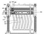
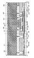
본 발명의 일양태에 관한 액정 표시 장치의 화소 영역은 복수의 제 1 배선과, 복수의 제 2 배선과, 복수의 트랜지스터와, 액정층을 협지하는 제 1 기판 및 제 2 기판을 가지고 있다. 본 발명의 일양태에 관한 액정 표시 장치의 화소 영역의 일부의 구성에 대하여 설명한다. 도 1은 액정 표시 장치의 평면도이며, 1 화소분의 화소를 나타내고, 본 실시형태에 나타내는 액정 표시 장치에서는 이 화소가 매트릭스 형상으로 복수 형성된다. 또한, 도 2는 도 1의 선 X1-X2, 선 X3-X4, 선 X5-X6에서의 단면도를 각각 나타낸다.The pixel area of the liquid crystal display device which concerns on one aspect of this invention has some 1st wiring, some 2nd wiring, some transistor, the 1st board | substrate which clamps a liquid crystal layer, and a 2nd board | substrate. The structure of one part of the pixel area of the liquid crystal display device which concerns on one aspect of this invention is demonstrated. 1 is a plan view of a liquid crystal display device, which shows pixels for one pixel, and in the liquid crystal display device shown in this embodiment, a plurality of these pixels are formed in a matrix. 2 shows sectional drawing in the line X1-X2, the line X3-X4, and the line X5-X6 of FIG.
이하에 본 실시형태에 나타내는 액정 표시 장치의 각 구조에 대하여 상세하게 설명한다.Hereinafter, each structure of the liquid crystal display device shown in this embodiment is demonstrated in detail.
도 1, 도 2에 나타낸 트랜지스터를 가지는 액티브 매트릭스형의 액정 표시 장치의 1 화소는 트랜지스터(301)와, 화소 전극층으로서 기능하는 제 1 전극층(302)과, 공통 전극층으로서 기능하는 제 2 전극층(303)과, 용량 소자(304)를 가진다.One pixel of the active matrix liquid crystal display device having the transistors shown in FIGS. 1 and 2 includes a
먼저, 트랜지스터(301)의 구성에 대하여 설명한다. 도 2에 나타낸 바와 같이, 트랜지스터(301)는 제 1 기판(318) 위에 형성된, 절연막(319)과, 절연막(319) 위의 제 1 배선(305)과, 제 1 배선(305) 위의 게이트 절연막으로서 기능하는 절연막(320)과, 절연막(320)을 사이에 끼우고 제 1 배선(305)과 중첩되는 위치에 형성된 반도체층(306)과, 절연막(320) 및 반도체층(306) 위의 소스 전극(307) 및 드레인 전극(308)과, 반도체층(306), 소스 전극(307) 및 드레인 전극(308) 위의 절연막(321)과, 절연막(321) 위의 절연막(322)을 가진다.First, the configuration of the
트랜지스터(301)의 각 구성의 상세한 사항에 대해서는, 이후에 본 발명의 일양태에 관한 액정 표시 장치의 제작 방법에서 설명한다.The detail of each structure of the
트랜지스터(301)에 있어서, 소스 전극(307)은 소스 전극(307) 위의 절연막(321), 절연막(322) 및 절연막(323)이 가지는 개구부를 통하여, 제 1 접속 전극(311)에 전기적으로 접속되어 있다. 드레인 전극(308)은 드레인 전극(308) 위의 절연막(321), 절연막(322) 및 절연막(323)이 가지는 개구부를 통하여, 제 2 접속 전극(312)에 전기적으로 접속되어 있다. 도전막(314)은 도전막(314) 위의 절연막(321), 절연막(322) 및 절연막(323)이 가지는 개구부를 통하여, 화소 전극으로서 기능하는 제 1 전극층(302)에 전기적으로 접속되어 있다.In the
본 실시형태에서, 소스 전극(307)은 제 1 접속 전극(311)에 전기적으로 접속되어 있지만, 소스 전극(307)과 제 1 접속 전극(311)의 사이에 전극이나 배선 등을 통하여 전기 신호를 수수하는 구성으로 해도 좋다. 마찬가지로, 드레인 전극(308)은 제 2 접속 전극(312)에 전기적으로 접속되어 있지만, 드레인 전극(308)과 제 2 접속 전극(312)의 사이에 전극이나 배선 등을 통하여 전기 신호를 수수하는 구성으로 해도 좋다. 마찬가지로, 도전막(314)은 화소 전극으로서 기능하는 제 1 전극층(302)에 전기적으로 접속되어 있지만, 도전막(314)과 제 1 전극층(302)의 사이에 전극이나 배선 등을 통하여 전기 신호를 수수하는 구성으로 해도 좋다.In the present embodiment, the
또한, 제 1 배선(305)은 게이트 전극으로서 기능하고, 주사선으로서도 기능한다. 또한, 제 2 배선(310)과 인접 화소의 제 2 배선(309)은 제 1 접속 전극(311)과 전기적으로 접속되어 있고, 모두 신호선으로서 기능한다. 또한, 제 1 배선(305)과, 제 2 배선(309) 및 제 2 배선(310)은 제 1 접속 전극(311)에 의해 직교하고 있다.In addition, the
본 실시형태에서, 제 2 배선(309) 및 제 2 배선(310)은 제 1 접속 전극(311)과 전기적으로 접속되어 있지만, 제 2 배선(309)과 제 1 접속 전극(311), 제 2 배선(310)과 제 1 접속 전극(311)의 사이에 전극이나 배선 등을 통하여 전기 신호를 수수하는 구성으로 해도 좋다.In this embodiment, although the
도 1에 나타낸 바와 같이, 제 2 배선(309), 제 2 배선(310)이 서로 평행하며(도면 중 상하 방향으로 연장), 또한, 서로 이간한 상태로 배치되어 있다. 제 1 배선(305)은 제 2 배선(309), 제 2 배선(310)에 대하여 수직인 방향(도면 중 좌우 방향)으로 연장되고, 또한, 서로 이간하도록 배치되어 있다. 제 3 배선(316)은 제 1 배선(305)에 인접하는 위치에 배치되어 있고, 제 1 배선(305)에 평행한 방향, 즉, 제 2 배선(309), 제 2 배선(310)에 대하여 수직인 방향(도면 중 좌우 방향)으로 연장하고 있다. 또한, 제 3 배선(316)과 도전막(314)이 중첩하는 영역에 용량이 형성되어 있다.As shown in FIG. 1, the
또한, 주사선과 신호선의 교차부에서 분단되고, 신호선으로서 기능하는 제 2 배선(309)과 제 2 배선(310)을 평탄화된 절연막(323) 위의 제 1 접속 전극(311)으로 가교한다. 또한, 제 1 배선(305)과 제 3 배선(316) 위에 형성되는 절연막(323)의 막두께는 500 nm 이상 5μm 이하로 하는 것이 바람직하다. 이것에 의해, 두꺼운 절연막(323)을 통하여 제 1 접속 전극(311)과 제 1 배선(305)과의 사이의 거리를 보다 길게 할 수 있기 때문에, 배선의 교차부의 기생 용량을 저감할 수 있다. 따라서, 화소 영역에서의 기생 용량의 총합을 저감시킬 수 있고, 화소수를 증가시켜도 화소 영역에서의 구동 속도의 저하를 억제할 수 있다.Further, the
또한, 절연막(323) 위에 있는 제 1 접속 전극(311)의 재료를 저항이 작은 금속을 이용하여, 막두께를 두껍게 함으로써 배선에 의한 저항을 작게 할 수 있어, 액정 표시 장치의 구동 속도의 저하를 억제할 수 있다.In addition, the thickness of the
또한, 본 실시형태에서는 제 1 접속 전극(311)을 이용하여, 제 2 배선(309) 및 제 2 배선(310)과 소스 전극(307)을 전기적으로 접속하고 있었지만, 이것에 한정되지 않는다. 최저한, 제 1 접속 전극(311)은 제 2 배선(309) 및 제 2 배선(310)과 전기적으로 접속하고 있으면 좋고, 소스 전극(307)은 제 2 배선(309) 및 제 2 배선(310)의 어느 한쪽과 전기적으로 접속하는 구성으로 해도 좋다.In addition, although the
다음에, 용량 소자(304)의 구성에 대하여 설명한다. 용량 소자(304)는 용량선으로서 기능하는 제 3 배선(316)과, 제 3 배선(316) 위의 절연막(320)과, 절연막(320) 위의 도전막(314)을 가지고, 제 3 배선(316), 절연막(320), 도전막(314)이 중첩되어 있는 부분이 용량 소자(304)로서 기능한다.Next, the configuration of the
용량선으로서 기능하는 배선은 제 3 배선(316)에 한정되지 않는다. 예를 들어, 주사선으로서 기능하는 제 1 배선과 겸용하는 구성으로 할 수도 있다. 또한, 도전막(314)에서도 이것에 한정되지 않고, 드레인 전극(308)과 겸용하는 구성으로 할 수도 있다. 또한, 도전막(314)이 제 3 배선(316), 절연막(320), 절연막(321), 절연막(322), 절연막(323), 제 1 전극층(302)(또는 제 2 전극층(303))과 중첩되는 구성으로 하여 용량을 형성할 수도 있다.The wiring functioning as the capacitance line is not limited to the
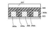
다음에 화소 전극 및 공통 전극으로서 기능하는 제 1 전극층(302) 및 제 2 전극층(303)에 대하여 도 3을 이용하여 설명한다. 도 3은 액정 표시 장치의 화소 전극 및 공통 전극간의 전계에 대하여 설명한 단면도이다.Next, the
도 3에 나타낸 바와 같이, 화소 전극으로서 기능하는 제 1 전극층(302) 및 공통 전극으로서 기능하는 제 2 전극층(303a), 공통 전극으로서 기능하는 제 2 전극층(303b)이 절연막(323) 위에 형성되어 있다. 제 1 전극층(302) 및 제 2 전극층(303a), 제 2 전극층(303b)의 막두께는 액정층(328)의 막두께 방향으로(3 차원적으로) 넓게 전계를 형성할 수 있고, 그 전계를 이용하여 액정 분자를 제어할 수 있는 막두께이며, 구체적으로는 액정층(328)의 막두께의 10% 이상 100% 이하로 두껍고, 절연막(323)의 액정층(328)측의 면으로부터 액정층(328) 중으로 돌출하여 형성되어 있다.As shown in FIG. 3, a
제 1 전극층(302) 및 제 2 전극층(303a), 제 2 전극층(303b)은 주상(柱狀)이다.The
제 1 전극층(302) 및 제 2 전극층(303a), 제 2 전극층(303b)의 형상은 리브(rib) 형상, 추형(錐形)의 선단이 평면이고 단면이 사다리꼴인 형상 등을 이용할 수 있다.The shape of the
도 3과 같이 주상의 제 1 전극층(302)을 형성하고, 주상의 제 2 전극층(303a), 주상의 제 2 전극층(303b)을 형성함으로써, 제 1 전극층(302) 및 제 2 전극층(303a), 제 2 전극층(303b)의 표면적을 액정층(328)의 막두께 방향으로(3 차원적으로)도 확대할 수 있다. 따라서, 도 3에 나타낸 바와 같이, 제 1 전극층(302)과 제 2 전극층(303a)과의 사이에 화살표(342a)로 나타내는 전계가, 제 1 전극층(302)과 제 2 전극층(303b)과의 사이에 화살표(342b)로 나타내는 전계가 각각 액정층의 막두께 방향에 걸쳐 광범위하게 더해진다. 또한, 화살표(342a), 화살표(342b)로 나타낸 바와 같이, 제 1 전극층(302)과 제 2 전극층(303a), 제 2 전극층(303b)과의 상면(상방 영역)에서는 전기력선은 원 형상으로 돌아 들어가도록 형성된다.The
따라서, 액정층(328) 전체에 걸쳐 액정 분자를 응답시킬 수 있어, 백투과율이 향상된다. 따라서, 백투과율과 흑투과율(흑표시시의 광의 투과율)과의 비인 콘트라스트비도 높게 할 수 있다. 또한, 블루상을 나타내는 점도가 높은 액정 재료의 경우에도, 효과적으로 전계를 인가할 수 있기 때문에, 저소비 전력화도 달성할 수 있다.Therefore, the liquid crystal molecules can be made to respond to the entire
또한, 화소 영역에서의 제 1 전극층(302) 및 제 2 전극층(303a), 제 2 전극층(303b)이 가지는 형상으로서는, 폐(閉) 공간을 가지지 않는 빗살 모양과 같은 패턴이 바람직하다. 제 1 전극층(302)과, 제 2 전극층(303a) 및 제 2 전극층(303b)은 접하지 않고, 서로의 빗살 모양의 패턴이 맞물리도록 동일한 절연 표면 위에 형성되어 있다.Moreover, as a shape which the
또한, 제 2 전극층(303)은 본 실시형태에서는 제 1 배선에 대하여 직교하는 방향으로 연장하여 설치되어 있지만 이것에 한정되지 않고, 제 1 배선에 대하여 평행한 방향으로 연장하여 형성되어 있어도 좋다. 또한, 연장하여 형성되어 있는 제 2 전극층(303)은 화소 영역의 말단에서 외부 전원과 접속되어 있다.In addition, although the
제 1 기판(318)과 대치하도록, 제 2 기판(327)이 설치되어 있다. 제 1 기판(318)과 제 2 기판(327)의 사이에는 액정층(328)이 형성되어 있다. 액정층(328)은 제 1 전극층(302)과 제 2 전극층(303)의 사이에도 충전되어 있다. 제 1 전극층(302)과 제 2 전극층(303)과 액정층(328)을 포함하는 영역이 액정 소자로서 기능한다.The
본 실시형태에서는, 트랜지스터(301)로서 보텀 게이트 구조의 역스태거형의 트랜지스터를 이용했지만, 이것에 한정되지 않는다. 예를 들면, 탑 게이트 구조의 트랜지스터를 이용하는 구성으로 해도 좋다.In this embodiment, an inverted staggered transistor having a bottom gate structure is used as the
또한, 본 실시형태에서는 분단된 상부의 제 2 배선이 접속 전극으로 전기적으로 접속되어 접속 전극이 하부의 제 1 배선과 교차하는 구성으로 했지만, 이것에 한정되지 않는다. 예를 들면, 상부의 제 2 배선 대신에 하부의 제 1 배선이 분단되어 있고, 분단된 하부의 제 1 배선이 접속 전극으로 전기적으로 접속되어 있는 구성으로 해도 좋다.In addition, in this embodiment, although the 2nd wiring of the upper part which was divided was electrically connected to the connection electrode, and the connection electrode crossed | intersected with the 1st wiring of the lower part, it is not limited to this. For example, the lower first wiring may be divided instead of the upper second wiring, and the divided first wiring may be electrically connected to the connection electrode.
또한, 제 2 기판(327) 위에, 특정의 파장 영역의 광을 선택적으로 투과하는 컬러 필터를 설치해도 좋다.In addition, a color filter may be provided on the
계속하여, 본 발명의 일양태에 관한 액정 표시 장치의 제작 방법에 대하여, 도 4 및 도 5를 이용하여 설명한다. 도 4 및 도 5는 본 발명의 일양태에 관한 액정 표시 장치의 제작 방법을 설명하는 단면도이다.Next, the manufacturing method of the liquid crystal display device which concerns on one aspect of this invention is demonstrated using FIG. 4 and FIG. 4 and 5 are cross-sectional views illustrating a method for manufacturing a liquid crystal display device according to one embodiment of the present invention.
먼저, 도 4(A)에 나타낸 바와 같이, 제 1 기판(318) 위에 절연막(319)을 형성한 후, 절연막(319) 위에 제 1 배선(305) 및 제 3 배선(316)을 형성한다.First, as shown in FIG. 4A, an insulating
제 1 기판(318)으로서 사용할 수 있는 소재에 큰 제한은 특별히 없지만, 적어도, 후의 가열 처리에 견딜 수 있을 정도의 내열성을 가지고 있을 필요가 있다. 예를 들면, 제 1 기판(318)에는 퓨전법이나 플로트법으로 제작되는 유리 기판, 석영 기판, 반도체 기판, 세라믹 기판 등을 이용할 수 있다. 유리 기판으로서는, 후의 가열 처리의 온도가 높은 경우에는 변형점이 730℃ 이상의 것을 이용하면 좋다.Although there is no big restriction | limiting in particular in the raw material which can be used as the 1st board |
절연막(319)은 반드시 형성할 필요는 없지만, 절연막(319)을 형성함으로써 제 1 기판(318) 중에 포함되는 알칼리 금속이나 알칼리토 금속이, 후에 형성되는 반도체층(306) 중으로 확산하여, 트랜지스터(301)의 특성에 악영향을 미치는 것을 막을 수 있다. 절연막(319)은 산화실리콘, 질화실리콘, 산화질화실리콘, 질화산화실리콘, 질화알루미늄 등의 절연성을 가지는 재료를 이용하여 형성한다.The insulating
또한, 본 명세서에서 산화질화실리콘과 같은 「산화질화물」이란, 그 조성으로서 질소보다 산소의 함유량이 많은 물질이며, 또한, 질화산화실리콘과 같은 「질화산화물」은, 그 조성으로서 산소보다 질소의 함유량이 많은 물질을 의미한다.In the present specification, "oxynitride" such as silicon oxynitride is a substance containing more oxygen than nitrogen as its composition, and "nitride oxide" such as silicon nitride is a content of nitrogen as oxygen in its composition. This means many substances.
제 1 배선(305) 및 제 3 배선(316)은 절연막(319) 위에 도전막을 형성한 후, 이 도전막을 소정의 형상으로 가공(패터닝)함으로써, 형성할 수 있다. 이 도전막의 형성에는 CVD법, 스퍼터링법, 증착법, 스핀 코트법 등을 이용할 수 있다. 제 1 배선(305) 및 제 3 배선(316)이 되는 도전막은 알루미늄, 크롬, 구리, 탄탈, 티탄, 몰리브덴, 텅스텐으로부터 선택된 원소, 또는 상술한 원소를 성분으로 하는 합금이나, 상술한 원소를 조합한 합금막 등을 들 수 있다.The
또한, 제 1 배선(305) 및 제 3 배선(316)이 되는 도전막은 단층 구조이어도, 2층 이상의 적층 구조로 해도 좋다. 예를 들면, 실리콘을 포함하는 알루미늄막의 단층 구조, 알루미늄막 위에 티탄막을 적층하는 2층 구조, 티탄막과 그 티탄막 위에 중첩하여 알루미늄막을 적층하고, 또한, 그 위에 티탄막을 성막하는 3층 구조 등을 들 수 있다.In addition, the conductive film used as the
혹은, 알루미늄, 구리 등의 금속막의 하측 혹은 상측에 크롬, 탄탈, 티탄, 몰리브덴, 텅스텐 등의 고융점 금속막을 적층시킨 구성으로 해도 좋다. 또한, 알루미늄 또는 구리는 내열성이나 부식성의 문제를 회피하기 위해, 고융점 금속 재료와 조합하여 이용하면 좋다. 고융점 금속 재료로서는, 몰리브덴, 티탄, 크롬, 탄탈, 텅스텐, 네오디뮴, 스칸듐, 이트륨 등을 이용할 수 있다.Alternatively, a structure in which a high melting point metal film such as chromium, tantalum, titanium, molybdenum or tungsten is laminated on the lower side or the upper side of a metal film such as aluminum or copper may be used. In addition, aluminum or copper may be used in combination with a high melting point metal material in order to avoid problems of heat resistance and corrosion resistance. As the high melting point metal material, molybdenum, titanium, chromium, tantalum, tungsten, neodymium, scandium, yttrium and the like can be used.
도전막 형성 후에 가열 처리를 행하는 경우에는, 이 가열 처리에 견딜 수 있는 내열성을 도전막에 갖게 하는 것이 바람직하다.When heat-processing after conductive film formation, it is preferable to make a conductive film the heat resistance which can endure this heat processing.
본 실시형태에서는, 제 1 배선(305) 및 제 3 배선(316)으로서, 막두께 50 nm의 티탄막, 막두께 100 nm의 알루미늄막, 막두께 50 nm의 티탄막을 순차로 적층함으로써 얻어지는 도전막을 이용한다.In the present embodiment, as the
또한, 마스크를 이용하지 않고, 액적 토출법을 이용하여 선택적으로 제 1 배선(305) 및 제 3 배선(316)을 형성해도 좋다. 액적 토출법이란, 조성물을 포함하는 액적을 세공(細孔)으로부터 토출 또는 분출함으로써 패턴을 형성하는 방법을 의미하고, 잉크젯법 등이 그 범주에 포함된다.Further, the
또한, 제 1 배선(305) 및 제 3 배선(316)은 도전막을 형성한 후, 반응성 이온 에칭(RIE:Reactive 이온 에칭)법, ICP(Inductively Coupled Plasma) 에칭법, ECR(Electron Cyclotron Resonance) 에칭법, 평행 평판형(용량 결합형) 에칭법, 마그네트론 플라즈마 에칭법, 2주파 플라즈마 에칭법 또는 헬리콘파 플라즈마 에칭법 등을 이용하여, 에칭 조건(코일형의 전극층에 인가되는 전력량, 기판측의 전극층에 인가되는 전력량, 기판측의 전극 온도 등)을 적절히 조절함으로써, 소망의 테이퍼 형상을 가지도록 에칭할 수 있다. 또한, 테이퍼 형상은 마스크의 형상에 따라서도 각도 등을 제어할 수 있다. 또한, 에칭용 가스로서는, 염소, 염화붕소, 염화실리콘 혹은 사염화탄소 등의 염소계 가스, 사불화탄소, 불화유황 혹은 불화질소 등의 불소계 가스 또는 산소를 적절히 이용할 수 있다.In addition, after the
다음에, 도 4(B)에 나타낸 바와 같이, 제 1 배선(305) 및 제 3 배선(316) 위의 절연막(320)을 형성한 후, 절연막(320)을 사이에 끼우고 제 1 배선(305)과 중첩되는 위치에 반도체층(306)을 형성한다.Next, as shown in Fig. 4B, after forming the insulating
절연막(320)은 플라즈마 CVD법 또는 스퍼터링법 등을 이용하여 산화실리콘, 질화산화실리콘, 산화질화실리콘, 질화실리콘, 산화하프늄, 산화알루미늄 또는 산화탄탈, 산화이트륨, 하프늄 실리케이트(HfSixOy(x>0, y>0)), 질소가 첨가된 하프늄 실리케이트(HfSixOy(x>0, y>0)), 질소가 첨가된 하프늄 알루미네이트(HfAlxOy(x>0, y>0)) 등을 포함하는 막을 단층으로, 또는 적층시킴으로써 형성할 수 있다.The insulating
절연막(320)의 두께는 예를 들면, 1 nm 이상 500 nm 이하, 바람직하게는 10 nm 이상 400 nm 이하로 할 수 있다. 본 실시형태에서는 플라즈마 CVD법을 이용하여, 막두께 300 nm 정도의 질화실리콘을 포함하는 단층의 절연막을 절연막(320)으로서 이용한다.The thickness of the insulating
또한, 절연막(320)의 플라즈마 CVD법에 의한 형성 공정에서 글로우 방전 플라즈마의 생성은 3 MHz에서 30 MHz, 대표적으로는 13.56 MHz, 27.12 MHz의 고주파 전력, 또는 30 MHz보다 크고 300 MHz 정도까지의 VHF대의 고주파 전력, 대표적으로는 60 MHz를 인가함으로써 행해진다. 또한, 1 GHz 이상의 마이크로파의 고주파 전력을 인가함으로써 행해진다. 또한, 고주파 전력이 펄스상으로 인가되는 펄스 발진이나, 연속적으로 인가되는 연속 발진으로 할 수 있다. 또한, HF대의 고주파 전력과 VHF대의 고주파 전력을 중첩시킴으로써, 대면적 기판에서도 플라즈마의 편차를 저감하여, 균일성을 높일 수 있음과 동시에, 성막 속도를 높일 수 있다. 또한, 고주파수가 1 GHz 이상인 마이크로파 플라즈마 CVD 장치를 이용하여 절연막(320)을 형성하면, 게이트 전극으로서 기능하는 제 1 배선(305)과, 소스 전극(307) 및 드레인 전극(308)과의 사이의 내압을 향상시킬 수 있기 때문에, 신뢰성이 높은 트랜지스터(301)를 얻을 수 있다.In the formation process of the insulating
절연막(320)으로서 유기 실란 가스를 이용한 CVD법에 의해 산화실리콘층을 형성함으로써, 후에 형성하는 반도체층의 결정성을 높여 트랜지스터(301)의 온 전류, 이동도 및 신뢰성을 높일 수 있다. 유기 실란 가스로서는, 규산에틸(TEOS:화학식 Si(OC2H5)4), 테트라메틸실란(TMS:화학식 Si(CH3)4), 테트라 메틸시클로테트라실록산(TMCTS), 옥타메틸시클로테트라실록산(OMCTS), 헥사메틸디실라잔(HMDS), 트리에톡시실란(SiH(OC2H5)3), 트리스디메틸아미노실란(SiH(N(CH3)2)3) 등의 실리콘 함유 화합물을 이용할 수 있다.By forming the silicon oxide layer by the CVD method using the organic silane gas as the insulating
반도체층(306)은 실란이나 게르만으로 대표되는 반도체 재료 가스를 이용하여 기상 성장법이나 스퍼터링법으로 제작되는 비정질(아몰퍼스(amorphous)라고도 함) 반도체, 이 비정질 반도체를 광 에너지나 열에너지를 이용하여 결정화시킨 다결정 반도체, 혹은 미결정(세미 아몰퍼스 혹은 마이크로 크리스탈이라고도 함) 반도체 등을 이용할 수 있다. 이러한 반도체층은 스퍼터링법, LPCVD법, 또는 플라즈마 CVD법 등에 의해 성막할 수 있다.The
여기서 미결정 반도체는 단거리 질서에서 중거리 질서를 가지고, 결정립계, 쌍정경계, 전위(轉位) 결함, 격자 변형을 가진다. 주상 또는 침상 결정이 기판 표면에 대하여 법선 방향으로 성장하고 있다. 미결정 반도체의 대표예인 미결정 실리콘은 그 라만 스펙트럼이 단결정 실리콘을 나타내는 520 cm-1보다 저파수(低波數)측으로 시프트하고 있다. 즉, 단결정 실리콘을 나타내는 520 cm-1와 아몰퍼스 실리콘을 나타내는 480 cm-1의 사이에 미결정 실리콘의 라만 스펙트럼의 피크가 있다. 또한, 미결합손(댕글링 본드)을 종단하기 위해 수소 또는 할로겐을 적어도 1 원자% 또는 그 이상 포함시키고 있다. 또한, 헬륨, 아르곤, 크립톤, 네온 등의 희가스 원소를 포함시켜 격자 변형을 더욱 조장시킴으로써, 안정성이 증가하여 양호한 미결정 반도체막을 얻을 수 있다. 이러한 미결정 반도체에 관한 기술은 예를 들면, 미국 특허 4,409,134호에 개시되어 있다.Here, the microcrystalline semiconductor has a medium-range order in a short range order, and has grain boundaries, twin boundaries, dislocation defects, and lattice deformation. Columnar or acicular crystals are growing in the normal direction with respect to the substrate surface. The microcrystalline silicon, which is a representative example of the microcrystalline semiconductor, is shifted to the lower wave side than the 520 cm-1 where the Raman spectrum represents single crystal silicon. I.e., 520 cm indicates a single crystal silicon- a Raman spectrum of the microcrystalline silicon between the 480 cm-1 peak representing thefirst and the amorphous silicon. Moreover, at least 1 atomic% or more of hydrogen or halogen is contained in order to terminate an unbonded loss (dangling bond). Further, by incorporating rare gas elements such as helium, argon, krypton, neon, and the like to further promote lattice deformation, stability can be increased and a good microcrystalline semiconductor film can be obtained. Techniques for such microcrystalline semiconductors are disclosed, for example, in US Pat. No. 4,409,134.
아몰퍼스 반도체로서는, 대표적으로는 수소화 아몰퍼스 실리콘, 결정성 반도체로서는 대표적으로는 폴리실리콘 등을 들 수 있다. 폴리실리콘(다결정 실리콘)에는, 800℃ 이상의 프로세스 온도를 거쳐 형성되는 폴리실리콘을 주재료로서 이용한 소위 고온 폴리실리콘이나, 600℃ 이하의 프로세스 온도로 형성되는 폴리실리콘을 주재료로서 이용한 소위 저온 폴리실리콘, 또한 결정화를 촉진하는 원소 등을 이용하여, 비정질 실리콘을 결정화시킨 폴리실리콘 등을 포함하고 있다. 물론, 상술한 바와 같이, 미결정 반도체 또는 반도체층의 일부에 결정상을 포함하는 반도체를 이용할 수도 있다. 또한, 미결정 반도체층 또는 결정성 반도체층과 아몰퍼스 반도체층을 적층하여 이용할 수도 있다.Representative examples of the amorphous semiconductor include hydrogenated amorphous silicon and polysilicon and the like as the crystalline semiconductor. In polysilicon (polycrystalline silicon), so-called high-temperature polysilicon using polysilicon formed through a process temperature of 800 ° C or higher as a main material, or so-called low-temperature polysilicon using polysilicon formed at a process temperature of 600 ° C or lower as a main material, Polysilicon etc. which crystallized amorphous silicon using the element etc. which promote crystallization are included. Of course, as mentioned above, you may use the microcrystal semiconductor or the semiconductor which contains a crystalline phase in a part of semiconductor layer. Further, a microcrystalline semiconductor layer or a crystalline semiconductor layer and an amorphous semiconductor layer may be laminated and used.
또한, 반도체의 재료로서는 실리콘(Si), 게르마늄(Ge) 등의 단체(單體) 외에, GaAs, InP, SiC, ZnSe, GaN, SiGe 등과 같은 화합물 반도체도 이용할 수 있다.As the material of the semiconductor, compound semiconductors such as GaAs, InP, SiC, ZnSe, GaN, SiGe, and the like can be used in addition to the simple materials such as silicon (Si) and germanium (Ge).
또한, 반도체층(306)은 산화물 반도체막을 이용하여 형성할 수 있다. 반도체층(306)으로서 산화물 반도체막을 이용하는 경우, 예를 들면, 인듐을 함유하는 산화물 반도체 재료나, 인듐 및 갈륨을 함유하는 산화물 반도체 재료 등을 이용할 수 있다.In addition, the
또한, 산화물 반도체막에 이용하는 재료로서는, 4원계 금속 산화물인 In-Sn-Ga-Zn-O계의 재료나, 3원계 금속 산화물인 In-Ga-Zn-O계의 재료, In-Sn-Zn-O계의 재료, In-Al-Zn-O계의 재료, Sn-Ga-Zn-O계의 재료, Al-Ga-Zn-O계의 재료, Sn-Al-Zn-O계의 재료나, 2원계 금속 산화물인 In-Zn-O계의 재료, Sn-Zn-O계의 재료, Al-Zn-O계의 재료, Zn-Mg-O계의 재료, Sn-Mg-O계의 재료, In-Mg-O계의 재료, In-Ga-O계의 재료나, 단원계 금속의 산화물인 In-O계의 재료, Sn-O계의 재료, Zn-O계의 재료 등이 있다. 또한, 상기의 재료에 SiO2를 포함시켜도 좋다. 여기서, 예를 들면, In-Ga-Zn-O계의 재료란, 인듐(In), 갈륨(Ga), 아연(Zn)을 가지는 산화물막이라는 의미이며, 그 조성비는 특별히 묻지 않는다. 또한, In와 Ga와 Zn 이외의 원소를 포함하고 있어도 좋다.As the material used for the oxide semiconductor film, an In-Sn-Ga-Zn-O-based material which is a quaternary metal oxide, an In-Ga-Zn-O-based material which is a ternary metal oxide, or In-Sn-Zn -O-based material, In-Al-Zn-O-based material, Sn-Ga-Zn-O-based material, Al-Ga-Zn-O-based material, Sn-Al-Zn-O-based material , In-Zn-O based material, binary metal oxide, Sn-Zn-O based material, Al-Zn-O based material, Zn-Mg-O based material, Sn-Mg-O based material , In-Mg-O-based materials, In-Ga-O-based materials, In-O-based materials which are oxides of single-type metals, Sn-O-based materials, Zn-O-based materials, and the like. It is also possible even if the SiO2 contained in the material. Here, for example, an In—Ga—Zn—O-based material means an oxide film having indium (In), gallium (Ga), and zinc (Zn), and the composition ratio is not particularly relevant. Moreover, elements other than In, Ga, and Zn may be included.
또한, 산화물 반도체막으로서는, 화학식 InMO3(ZnO)m(m>0)로 표기되는 재료를 이용한 박막으로 할 수 있다. 여기서, M은 Ga, Al, Mn 및 Co로부터 선택된 하나 또는 복수의 금속 원소를 나타낸다. 예를 들면, M으로서 Ga, Ga 및 Al, Ga 및 Mn, 또는 Ga 및 Co 등을 이용할 수 있다.Further, as the oxide semiconductor film may be a thin film using the material represented by the formulaInMO 3 (ZnO) m (m > 0). Here, M represents one or a plurality of metal elements selected from Ga, Al, Mn and Co. For example, Ga, Ga and Al, Ga and Mn, or Ga and Co can be used as M.
산화물 반도체막은 수소나 물 등이 혼입하기 어려운 방법으로 제작하는 것이 바람직하다. 예를 들면, 스퍼터링법 등을 이용하여 제작할 수 있다. 산화물 반도체막의 성막의 분위기는, 희가스(대표적으로는 아르곤) 분위기하, 산소 분위기하, 또는, 희가스와 산소의 혼합 분위기하 등으로 하면 좋다. 또한, 산화물 반도체막에 수소, 물, 수산기를 가지는 화합물, 수소화물 등의 혼입을 막기 위해, 수소, 물, 수산기를 가지는 화합물, 수소화물 등의 수소 원자를 포함하는 불순물이 충분히 제거된 고순도 가스를 이용한 분위기로 하는 것이 바람직하다. 또한, 성막 후, 산화물 반도체막에 열처리를 행하는 것이 바람직하다. 열처리를 행함으로써, 산화물 반도체막 중의 물이나 수소 등의 불순물을 제거하거나, 또는 산화물 반도체막 중에 산소를 공급할 수 있다.It is preferable to produce an oxide semiconductor film by the method which hydrogen, water, etc. are difficult to mix. For example, it can manufacture using a sputtering method. The atmosphere for forming the oxide semiconductor film may be a rare gas (typically argon) atmosphere, an oxygen atmosphere, or a mixed atmosphere of a rare gas and oxygen. In addition, in order to prevent incorporation of hydrogen, water, a compound having a hydroxyl group, and a hydride into the oxide semiconductor film, a high-purity gas in which impurities containing hydrogen atoms such as hydrogen, water, a compound having a hydroxyl group, and a hydride are sufficiently removed are removed. It is preferable to set it as the atmosphere used. Moreover, it is preferable to heat-process an oxide semiconductor film after film-forming. By performing heat treatment, impurities such as water and hydrogen in the oxide semiconductor film can be removed, or oxygen can be supplied to the oxide semiconductor film.
이러한 밴드 갭이 넓은 산화물 반도체막을 반도체층(306)으로서 이용함으로써, 오프 상태에서의 전류값(오프 전류값)을 낮게 할 수 있다. 따라서, 화상 신호 등의 전기 신호의 보유 시간을 길게 할 수 있고, 전원 온 상태에서는 기입 간격도 길게 설정할 수 있다. 따라서, 리프레시 동작의 빈도를 줄일 수 있기 때문에, 소비 전력을 보다 억제하는 효과를 얻는다.By using the oxide semiconductor film having such a wide band gap as the
반도체층, 전극층, 배선층의 제작 공정에서, 박막을 소망의 형상으로 가공하기 위해 에칭 공정을 이용한다. 에칭 공정은 드라이 에칭이나 웨트 에칭을 이용할 수 있다.In the manufacturing process of a semiconductor layer, an electrode layer, and a wiring layer, an etching process is used in order to process a thin film into a desired shape. The etching process may use dry etching or wet etching.
드라이 에칭에 이용하는 에칭 장치로서는, 반응성 이온 에칭법(RIE법)을 이용한 에칭 장치나, ECR이나 ICP 등의 고밀도 플라즈마원을 이용한 드라이 에칭 장치를 이용할 수 있다.As an etching apparatus used for dry etching, the etching apparatus using the reactive ion etching method (RIE method), and the dry etching apparatus using high density plasma sources, such as ECR and ICP, can be used.
소망의 가공 형상으로 에칭할 수 있도록, 에칭 조건(코일형의 전극에 인가되는 전력량, 기판측의 전극에 인가되는 전력량, 기판측의 전극 온도 등)을 적절히 조절한다.(The amount of power applied to the coil-shaped electrode, the amount of power applied to the electrode on the substrate side, the electrode temperature on the substrate side, and the like) are appropriately controlled so that etching can be performed with a desired processing shape.
소망의 가공 형상으로 에칭할 수 있도록, 재료에 맞추어 에칭 조건(에칭액, 에칭 시간, 온도 등)을 적절히 조절한다.Etching conditions (etching liquid, etching time, temperature, etc.) are suitably adjusted according to a material so that it may etch in a desired process shape.
다음에, 도 4(C)에 나타낸 바와 같이, 절연막(320)과 반도체층(306)을 덮도록 도전막을 형성한 후, 제 1 배선(305) 및 제 3 배선(316)의 가공과 마찬가지로 상기 도전막을 가공(패터닝)함으로써, 제 2 배선(309), 제 2 배선(310), 소스 전극(307), 드레인 전극(308), 도전막(314)을 형성한다.Next, as shown in FIG. 4C, after the conductive film is formed so as to cover the insulating
또한, 본 실시형태에서는, 소스 전극(307), 드레인 전극(308)을 형성할 때에 트랜지스터(301)의 반도체층(306)도 일부가 에칭되어, 반도체층(306)은 홈부(오목부)를 가진다.In the present embodiment, when the
제 2 배선(309), 제 2 배선(310), 소스 전극(307), 드레인 전극(308), 도전막(314)은 제 1 배선(305) 및 제 3 배선(316)과 같은 재료, 및 같은 적층 구조로 형성할 수 있다.The
또한, Cu-Mg-Al 합금, Cu-Mg-O 합금, Cu-Ca-O 합금, Cu-Mg-Al-O 합금, Mo-Ti 합금, Ti, Mo는 산화막과의 밀착성이 높다. 따라서, 하층에 Cu-Mg-Al 합금, Cu-Mg-O 합금, Cu-Ca-O 합금, Cu-Mg-Al-O 합금, Mo-Ti 합금, Ti, 혹은 Mo로 구성되는 도전막, 상층에 Cu로 구성되는 도전막을 적층하여 제 2 배선(309), 제 2 배선(310), 도전막(314)을 형성함으로써, 절연막(320)이 산화실리콘, 산화질화실리콘, 산화하프늄, 산화알루미늄 또는 산화탄탈, 산화이트륨 등의 산화막인 경우에, 제 2 배선(309), 제 2 배선(310), 도전막(314)과 절연막(320)과의 밀착성을 높일 수 있다.Moreover, Cu-Mg-Al alloy, Cu-Mg-O alloy, Cu-Ca-O alloy, Cu-Mg-Al-O alloy, Mo-Ti alloy, Ti, and Mo have high adhesiveness with an oxide film. Therefore, a conductive film composed of a Cu-Mg-Al alloy, a Cu-Mg-O alloy, a Cu-Ca-O alloy, a Cu-Mg-Al-O alloy, a Mo-Ti alloy, Ti, or Mo in a lower layer, and an upper layer By stacking a conductive film made of Cu on the
이상의 공정에 의해, 도 4(C)에 나타낸 바와 같은 트랜지스터(301)를 제작할 수 있다.Through the above steps, the
다음에, 도 4(D)에 나타낸 바와 같이, 절연막(321), 절연막(322) 및 절연막(323)을 형성한다. 본 실시형태에서는 절연막(321)과 절연막(322)과 절연막(323)을 적층하고 있지만, 단층 구조의 절연막으로 해도 좋고, 2층 이상의 적층 구조로 해도 좋다.Next, as shown in FIG. 4D, an insulating
단층 구조의 절연막 또는 적층 구조 중 제 2 기판측에 가장 가까운 절연막은 평탄성이 높은 절연막인 것이, 후에 형성되는 제 1 전극층(302), 제 2 전극층(303), 제 1 접속 전극(311), 및 제 2 접속 전극(312)의 높이를 균일하게 정렬하는 데 있어서 바람직하다.An insulating film having a single layer structure or an insulating film closest to the second substrate side among the stacked structures is an insulating film having a high flatness, and is formed after the
절연막(321), 절연막(322)으로서 예를 들면, 산화실리콘, 질화산화실리콘, 질화실리콘, 산화하프늄, 산화알루미늄, 산화탄탈 등의 무기 절연 재료를 포함하는 재료를 이용하여 형성할 수 있다. 또한, 폴리이미드, 아크릴 수지 등의 유기 절연 재료를 이용하여 형성하는 것도 가능하다. 또한, 상기 재료 외에, 저유전율 재료(low-k 재료), 실록산계 수지, PSG(phosphosilicate glass:인 유리), BPSG(borophosphosilicate glass:인 붕소 유리) 등을 이용할 수 있다. 실록산계 수지는 실리콘(Si)과 산소(O)와의 결합으로 골격 구조가 구성되는 재료이다. 치환기로서 수소 외에, 불소, 유기기(예를 들면 알킬기, 아릴기), 불소를 포함하는 유기기 등을 가지고 있어도 좋다. 그리고, 절연막(321), 절연막(322)의 형성에는, 그 재료에 따라, CVD법, 스퍼터링법, 스핀 코트, 딥, 스프레이 도포, 액적 토출법(잉크젯법 등), 인쇄법(스크린 인쇄, 오프셋 인쇄 등) 등을 이용할 수 있다.As the insulating
또한, 절연막(321), 절연막(322)으로서, 유기 실란을 이용하여 화학 기상 성장법에 의해 제작되는 산화실리콘막을 이용할 수도 있다. 유기 실란으로서는, 규산에틸(TEOS:Si(OC2H5)4), 트리메틸실란(TMS:(CH3)3SiH), 테트라메틸시클로테트라실록산(TMCTS), 옥타메틸시클로테트라실록산(OMCTS), 헥사메틸디실라잔(HMDS), 트리에톡시실란(SiH(OC2H5)3), 트리스디메틸아미노실란(SiH(N(CH3)2)3) 등을 이용할 수 있다. 물론, 모노실란, 디실란, 또는 트리실란 등의 무기 실란을 이용하여, 산화실리콘, 산화질화실리콘, 질화실리콘, 질화산화실리콘 등을 형성해도 좋다.As the insulating
평탄성이 높은 절연막(323)은 폴리이미드, 아크릴 수지, 벤조시클로브텐계 수지, 폴리아미드, 에폭시 수지 등의 유기 재료를 이용할 수 있다. 또한, 상기 유기 재료 외에, 실록산계 수지, PSG(인 유리), BPSG(인 붕소 유리) 등의 저유전 재료(low-k 재료)를 이용할 수 있다. 그리고, 절연막(323)의 형성에는 그 재료에 따라, 스핀 코트, 딥, 스프레이 도포, 액적 토출법(잉크젯법 등), 인쇄법(스크린 인쇄, 오프셋 인쇄 등), 롤 코트, 커튼 코트, 나이프 코트 등을 이용할 수 있다.As the insulating
절연막(321) 및 절연막(322)의 합계의 막두께는 100 nm 이상 1.5μm 이하가 바람직하고, 300 nm 이상 1.0μm 이하가 보다 바람직하다. 또한, 평탄성이 높은 절연막(323)은 500 nm 이상 5μm 이하가 바람직하고, 1.0μm 이상 2.0μm 이하가 보다 바람직하다.100 nm or more and 1.5 micrometer or less are preferable, and, as for the film thickness of the sum total of the insulating
절연막(321), 절연막(322) 및 절연막(323)의 막두께를 두껍게 함으로써 제 1 배선과 제 1 접속 전극과의 사이의 거리를 보다 길게 할 수 있기 때문에 배선의 교차부의 기생 용량을 저감할 수 있다. 따라서, 화소 영역에서의 기생 용량의 총합을 저감시킬 수 있어, 화소수를 증가시켜도 액정 표시 장치의 구동 속도의 저하를 억제할 수 있다.By increasing the thickness of the insulating
본 실시형태에서는 절연막(321), 절연막(322)과 평탄성이 높은 절연막(323)의 3층 구성이며, 절연막(321), 절연막(322)을 질화실리콘을 이용하여 합계의 막두께를 300 nm로 하여 형성하고, 절연막(323)을 아크릴을 이용하여 막두께 1.5μm로 형성한다.In this embodiment, the insulating
다음에, 도 5(A)에 나타낸 바와 같이, 절연막(321), 절연막(322) 및 절연막(323)에 개구부를 형성하고, 제 2 배선(309)의 일부, 제 2 배선(310)의 일부, 소스 전극(307)의 일부, 드레인 전극(308)의 일부, 도전막(314)의 일부를 노출시킨다. 그리고, 개구부에서, 제 2 배선(309), 제 2 배선(310), 소스 전극(307), 드레인 전극(308), 및 도전막(314)에 접하도록, 절연막(323) 위에 도전막(340)을 형성한다.Next, as shown in FIG. 5A, openings are formed in the insulating
도전막(340)은 제 1 배선(305) 및 제 3 배선(316)과 같은 재료, 및 같은 적층 구조로 형성할 수 있다. 또한, 액정 표시 장치의 고속 구동의 저하를 억제하기 위해, 저항이 작은 금속을 이용하는 것이 바람직하다. 후에 형성되는 제 1 접속 전극(311)의 재료가 저항이 작은 금속을 이용하여, 막두께를 두껍게 함으로써 배선에 의한 저항을 작게 할 수 있어, 액정 표시 장치의 구동 속도의 저하를 억제할 수 있다. 또한, 후에 형성되는 제 1 전극층(302) 및 제 2 전극층(303)의 막두께를 크게 하여, 횡전계를 액정에 인가하기 쉽도록 도전막(340)의 막두께를 크게 하는 것이 바람직하다. 또한, 제 1 접속 전극(311), 제 1 전극층(302) 및 제 2 전극층(303)의 막두께는 액정층(328)의 막두께의 10% 이상 100% 이하가 바람직하고, 20% 이상 80% 이하가 보다 바람직하다.The
또한, 환원력이 높은 원소인 티탄을 이용하여 도전막(340) 아래에 배리어 메탈막을 형성하면, 제 2 배선(309), 제 2 배선(310), 소스 전극(307), 드레인 전극(308), 및 도전막(314) 위에 얇은 산화막으로 되어 있었다고 해도, 배리어 메탈막에 포함되는 티탄이 이 산화막을 환원하여, 제 2 배선(309), 제 2 배선(310), 소스 전극(307), 드레인 전극(308), 및 도전막(314)과 도전막(340)이 각각 양호한 컨택트를 취할 수 있다.In addition, when the barrier metal film is formed under the
따라서, 예를 들면, 티탄막 위에 알루미늄막, 텅스텐막을 순차로 적층하는 3층 구조, 티탄막 위에 알루미늄막, 질화탄탈막을 순차로 적층하는 3층 구조로 함으로써, 상술한 2개의 이점에 더하여, 제 2 배선(309), 제 2 배선(310), 소스 전극(307), 드레인 전극(308), 및 도전막(314)과의 접속부에서의 컨택트 저항을 낮춘다는 이점을 얻을 수 있다.Thus, for example, a three-layer structure in which an aluminum film and a tungsten film are sequentially stacked on a titanium film, and a three-layer structure in which an aluminum film and a tantalum nitride film are sequentially stacked on a titanium film, in addition to the two advantages described above, The advantage of lowering the contact resistance at the connection portion between the
또한, 도전막(340)의 막두께는 500 nm 이상 5μm 이하, 보다 바람직하게는 1μm 이상 4μm 이하인 것이 바람직하다. 본 실시형태에서는 막두께 200 nm의 티탄막, 막두께 600 nm의 알루미늄막, 막두께 200 nm의 텅스텐막을 순차로 적층하여 도전막(340)을 형성한다.The film thickness of the
다음에, 도 5(B)에 나타낸 바와 같이, 드라이 에칭에 의해 도전막(340)을 가공함으로써, 섬 형상의 제 1 전극층(302), 제 2 전극층(303), 제 1 접속 전극(311) 및 제 2 접속 전극(312)을 형성한다. 제 1 접속 전극(311)은 절연막(321), 절연막(322) 및 절연막(323)에 형성된 개구부를 통하여 소스 전극(307), 제 2 배선(309) 및 제 2 배선(310)에 접속하고 있다. 제 2 접속 전극(312)은 절연막(321), 절연막(322) 및 절연막(323)에 형성된 개구부를 통하여 드레인 전극(308)에 접속하고 있다. 화소 전극으로서 기능하는 제 1 전극층(302)은 절연막(321), 절연막(322) 및 절연막(323)에 형성된 개구부를 통하여 도전막(314)에 접속되어 있다. 또한, 제 1 전극층(302)은 도전막(314) 및 제 2 접속 전극(312)을 통하여 드레인 전극(308)과 접속되어 있다.Next, as shown in FIG. 5B, the
상기 드라이 에칭에는, 예를 들면, 반응성 이온 에칭법, ICP 에칭법, ECR 에칭법, 평행 평판형(용량 결합형) 에칭법, 마그네트론 플라즈마 에칭법, 2주파 플라즈마 에칭법 또는 헬리콘파 플라즈마 에칭법 등의 드라이 에칭법을 이용할 수 있다.For the dry etching, for example, reactive ion etching method, ICP etching method, ECR etching method, parallel plate type (capacitive coupling type) etching method, magnetron plasma etching method, two-frequency plasma etching method or helicon wave plasma etching method, etc. Dry etching method of can be used.
에칭 가스에는, 염소, 염화붕소, 염화실리콘, 삼염화붕소 또는 사염화탄소 등의 염소계 가스, 사불화탄소, 불화유황 또는 불화질소 등의 불소계 가스, 산소 등을 적절히 이용할 수 있다.As the etching gas, chlorine-based gas such as chlorine, boron chloride, silicon chloride, boron trichloride or carbon tetrachloride, fluorine-based gas such as carbon tetrafluoride, sulfur fluoride or nitrogen fluoride, oxygen or the like can be suitably used.
구체적으로, 본 실시형태에서는, 티탄막, 알루미늄막, 텅스텐막을 순차로 적층하여 형성된 도전막(340)을 이용하고 있으므로, 에칭 가스인 염소의 유량 45 sccm, 사불화탄소의 유량 55 sccm, 산소의 유량 55 sccm, 반응 압력 0.67 Pa, 하부 전극의 온도 -10℃, 코일형의 전극에 투입하는 RF(13.56 MHz) 전력 3000 W, 하부 전극(바이어스측)에 투입하는 전력 140 W로 한 후, 에칭 가스인 염소의 유량 20 sccm, 삼염화붕소의 유량 60 sccm, 반응 압력 1.9 Pa, 하부 전극의 온도 -10℃, 코일형의 전극에 투입하는 RF(13.56 MHz) 전력 450 W, 하부 전극(바이어스측)에 투입하는 전력 100 W가 되도록, 도중에 조건을 변경하여 드라이 에칭을 행한다.Specifically, in the present embodiment, since the
혹은, 티탄막, 알루미늄막, 티탄막을 순차로 적층하여 형성된 도전막(340)을 이용하는 경우, 에칭 가스인 염소의 유량 20 sccm, 삼염화붕소의 유량 60 sccm, 반응 압력 1.9 Pa, 하부 전극의 온도 -10℃, 코일형의 전극에 투입하는 RF(13.56 MHz) 전력 450 W, 하부 전극(바이어스측)에 투입하는 전력 100 W가 되도록 하여 드라이 에칭을 행한다.Alternatively, in the case of using the
상기 공정 후, 제 1 기판(318)과 대치하도록 제 2 기판(327)을 제공하여, 액정층(328)을 충전함으로써, 도 2에 나타낸 바와 같은 액정 표시 장치를 얻을 수 있다.After the above process, the
액정층(328)을 형성하기 위해 행해지는 액정의 주입은 디스펜서식(적하식)을 이용해도 좋고, 딥식(펌핑식)을 이용하여도 좋다.Injecting the liquid crystal that is performed to form the
액정은 서모트로픽 액정(thermotropic liquid crystal), 강유전 액정, 반강유전 액정 등을 이용할 수 있고, 이것들은 저분자 액정, 고분자 액정의 어느 것이어도 상관없다.As the liquid crystal, a thermotropic liquid crystal, a ferroelectric liquid crystal, an antiferroelectric liquid crystal, or the like can be used, and these may be any of a low molecular liquid crystal and a polymer liquid crystal.
액정층(328)은 횡전계 모드에서 사용할 수 있는 액정 재료를 이용하면 좋고, 특히 블루상을 나타내는 액정 재료가 바람직하다. 블루상을 나타내는 액정 재료는 액정 및 카이럴제를 포함한다. 카이럴제는 액정을 나선 구조로 배향시키고, 블루상을 발현시키기 위해 이용한다. 예를 들면, 3 중량% 이상의 카이럴제를 혼합시킨 액정 재료를 액정층에 이용하면 좋다.The
카이럴제는 액정에 대한 상용성이 좋고, 또한, 비틀림력이 강한 재료를 이용한다. 또한, R체, S체의 어느 다른 한쪽의 재료가 좋고, R체와 S체의 비율이 50:50의 라세미체는 사용하지 않는다.The chiral agent uses a material having good compatibility with liquid crystals and strong torsional force. In addition, either material of R body and S body is good, and the racemate of 50:50 of R body and S body is not used.
상기 액정 재료는, 조건에 따라, 콜레스테릭상, 콜레스테릭 블루상, 스멕틱상, 스멕틱 블루상, 큐빅상, 카이럴 네마틱상, 등방상 등을 나타낸다.The said liquid crystal material shows a cholesteric phase, a cholesteric blue phase, a smectic phase, a smectic blue phase, a cubic phase, a chiral nematic phase, an isotropic phase, etc. according to conditions.
블루상인 콜레스테릭 블루상 및 스멕틱 블루상은 나선 피치가 500 nm 이하로 피치가 비교적 짧은 콜레스테릭상 또는 스멕틱상을 가지는 액정 재료에 보여진다. 액정 재료의 배향은 이중 비틀림 구조를 가진다. 가시광의 파장 이하의 질서를 가지고 있기 때문에, 투명하고, 전압 인가에 의해 배향 질서가 변화하여 광학적 변조 작용이 생긴다. 블루상은 광학적으로 등방이기 때문에 시야각 의존성이 없고, 배향막을 형성하지 않아도 좋기 때문에, 표시 화상의 질 향상 및 비용 삭감이 가능하다.The cholesteric blue phase and smectic blue phase, which are blue phases, are seen in liquid crystal materials having a cholesteric phase or smectic phase with a short pitch with a spiral pitch of 500 nm or less. The orientation of the liquid crystal material has a double torsional structure. Since it has order below the wavelength of visible light, it is transparent, and the orientation order changes by voltage application, and an optical modulation action arises. Since the blue phase is optically isotropic, there is no dependence on the viewing angle, and it is not necessary to form the alignment film, so that the quality of the display image can be improved and the cost can be reduced.
또한, 블루상은 좁은 온도 범위에서밖에 발현이 어렵고, 온도 범위를 넓게 개선하기 위해 액정 재료에 광경화 수지 및 광중합 개시제를 첨가하여, 고분자 안정화 처리를 행하는 것이 바람직하다. 고분자 안정화 처리는 액정, 카이럴제, 광경화 수지, 및 광중합 개시제를 포함하는 액정 재료에, 광중합 개시제가 반응하는 파장의 광을 조사하여 행한다. 이 고분자 안정화 처리는 온도 제어를 행하여, 등방상을 나타낸 상태로 광조사하여 행하여도 좋고, 블루상을 나타낸 상태로 광조사하여 행하여도 좋다.In addition, the blue phase is hardly expressed only in a narrow temperature range, and in order to improve the temperature range widely, it is preferable to add a photocuring resin and a photopolymerization initiator to the liquid crystal material and perform a polymer stabilization treatment. A polymer stabilization process is performed by irradiating the liquid crystal material containing a liquid crystal, a chiral agent, a photocuring resin, and a photoinitiator with the light of the wavelength to which a photoinitiator reacts. The polymer stabilization treatment may be performed by temperature control, light irradiation in an isotropic phase, or light irradiation in a blue phase.
예를 들면, 액정층의 온도를 제어하여, 블루상을 발현한 상태로 액정층에 광을 조사함으로써 고분자 안정화 처리를 행한다. 단, 이것에 한정되지 않고, 블루상과 등방상 간의 상전이 온도로부터 +10℃ 이내, 바람직하게는 +5℃ 이내의 등방상을 발현한 상태로 액정층에 광을 조사함으로써 고분자 안정화 처리를 행하여도 좋다. 블루상과 등방상 간의 상전이 온도란, 승온시에 블루상으로부터 등방상으로 전이하는 온도 또는 강온시에 등방상으로부터 블루상으로 상전이하는 온도를 말한다. 고분자 안정화 처리의 일례로서는, 액정층을 등방상까지 가열한 후, 서서히 강온시켜 블루상에까지 상전이시키고, 블루상이 발현하는 온도를 보유한 상태로 광을 조사할 수 있다. 그 밖에도, 액정층을 서서히 가열하여 등방상으로 상전이시킨 후, 블루상과 등방상 간의 상전이 온도로부터 +10℃ 이내, 바람직하게는 +5℃ 이내 상태(등방상을 발현한 상태)에서 광을 조사할 수 있다. 또한, 액정 재료에 포함되는 광경화 수지로서 자외선 경화 수지(UV 경화 수지)를 이용하는 경우, 액정층에 자외선을 조사하면 좋다. 또한, 블루상과 등방상 간의 상전이 온도로부터 +10℃ 이내, 바람직하게는 +5℃ 이내에서 등방상을 발현시키고, 광을 조사하여 고분자 안정화 처리를 행하면, 응답 속도가 1 msec 이하로 짧고 고속 응답이 가능하다.For example, a polymer stabilization process is performed by controlling the temperature of a liquid crystal layer and irradiating light to a liquid crystal layer in the state which expressed the blue phase. However, it is not limited to this, You may perform a polymer stabilization process by irradiating light to a liquid crystal layer in the state which expressed the isotropic phase within +10 degrees C, preferably +5 degrees C from the phase transition temperature between a blue phase and an isotropic phase. The phase transition temperature between a blue phase and an isotropic phase means the temperature which transitions from a blue phase to an isotropic phase at the time of temperature rising, or the temperature which phase-transfers from an isotropic phase to a blue phase at the time of temperature drop. As an example of a polymer stabilization process, after heating a liquid crystal layer to an isotropic phase, it can be gradually cooled, phase-transitions to a blue phase, and light can be irradiated in the state which kept the temperature which a blue phase expresses. In addition, after the liquid crystal layer is gradually heated to isotropically phase-transformed, light can be irradiated in a state (state of isotropic phase) within + 10 ° C, preferably within + 5 ° C from the phase transition temperature between the blue phase and the isotropic phase. have. In addition, what is necessary is just to irradiate an ultraviolet-ray to a liquid crystal layer, when ultraviolet curable resin (UV curable resin) is used as photocuring resin contained in a liquid crystal material. In addition, when the isotropic phase is expressed within + 10 ° C, preferably + 5 ° C from the phase transition temperature between the blue phase and the isotropic phase, and the polymer stabilization treatment is performed by irradiation of light, the response speed is short at 1 msec or less and high-speed response is possible. Do.
광경화 수지는 디아크릴레이트, 트리아크릴레이트, 디메타크릴레이트, 트리메타크릴레이트 등의 다관능 모노머, 혹은 이것들에 단관능 모노머를 혼합시킨 것이어도 좋다. 또한, 액정성의 것이어도 비액정성의 것이어도 좋고, 양자를 혼합시켜도 좋다.The photocuring resin may be a polyfunctional monomer such as diacrylate, triacrylate, dimethacrylate, trimethacrylate, or a monofunctional monomer mixed with these. Moreover, it may be liquid crystalline, non-liquid crystalline, or may mix both.
광중합 개시제는 광조사에 의해 래디칼을 발생시키는 래디칼 중합 개시제이어도 좋고, 산을 발생시키는 산발생제이어도 좋고, 염기를 발생시키는 염기 발생제이어도 좋다.The photopolymerization initiator may be a radical polymerization initiator for generating radicals by light irradiation, an acid generator for generating an acid, or a base generator for generating a base.
구체적으로는, 액정 재료로서 JC-1041XX(질소 주식회사(Chisso Corporation) 제조)와 4-시아노-4'-펜틸비페닐의 혼합물을 이용할 수 있고, 카이럴제로서는 ZLI-4572(머크 주식회사(Merck Ltd., Japan) 제조)를 이용할 수 있고, 광경화 수지는 2-에틸헥실아크릴레이트, RM257(머크 주식회사 제조), 트리메티롤프로판트리아크릴레이트를 이용할 수 있고, 광중합 개시제로서는 2,2-디메톡시-2-페닐아세트페논을 이용할 수 있다.Specifically, a mixture of JC-1041XX (manufactured by Chisso Corporation) and 4-cyano-4'-pentylbiphenyl can be used as the liquid crystal material, and ZLI-4572 (Merck (Merck) as a chiral agent can be used. Ltd., Japan)), 2-ethylhexyl acrylate, RM257 (manufactured by Merck Co., Ltd.), and trimethyrol propane triacrylate can be used as the photocuring resin, and 2,2-dimethol as the photopolymerization initiator. Oxy-2-phenylacetphenone can be used.
또한, 제 2 기판(327) 위에, 특정 파장 영역의 광을 선택적으로 투과하는 컬러 필터를 설치해도 좋다.In addition, a color filter may be provided on the
종래의 구성에서는, 제 1 배선에 상당하는 주사선과 제 2 배선에 상당하는 신호선은 절연막(320)만을 통하여 교차한다. 절연막(320)은 게이트 절연막으로서 기능하기 때문에, 그 막두께에는 한계가 있다. 이것에 대하여, 상술한 구성에서는, 화소마다 제 2 배선을 분단하여, 절연막(323) 위의 제 1 접속 전극으로 가교함으로써, 절연막(320) 내지 절연막(323)을 통하여 주사선과 신호선을 교차시킬 수 있다. 따라서, 상기 교차부에 있어서, 주사선과 신호선을 절연하는 절연막의 막두께를 증대시킬 수 있기 때문에, 교차 부분에서 생기는 기생 용량을 저감시킬 수 있고, 그 결과, 화소수를 증가시켜도 액정 표시 장치의 구동 속도의 저하를 억제할 수 있다. 또한, 제 1 접속 전극의 재료에 저항이 작은 금속을 이용하여, 막두께를 두껍게 함으로써 배선에 의한 저항을 작게 할 수 있고, 액정 표시 장치의 구동 속도의 저하를 억제할 수 있다. 따라서, 고품질의 동영상을 제공할 수 있다. 또한, 화소 전극인 제 1 전극층과 공통 전극인 제 2 전극층의 막두께를 두껍게 함으로써, 제 1 전극층과 제 2 전극층의 표면적을 액정층의 막두께 방향으로(3 차원적으로)도 확대할 수 있고, 제 1 전극층과 제 2 전극층 사이에 전압을 인가했을 때, 액정층에 있어서 넓게 전계를 형성할 수 있고, 그 전계를 이용하여 액정 분자를 제어할 수 있고, 횡전계 모드를 이용한 액정 표시 장치, 특히 블루상을 나타내는 액정을 이용한 액정 표시 장치에 있어서, 백투과율을 크게 하여, 콘트라스트비의 향상을 도모할 수 있다. 또한, 화소 전극인 제 1 전극층, 공통 전극인 제 2 전극층, 제 1 접속 전극을 동일층에서 동시에 형성할 수 있기 때문에, 공정을 간략화할 수 있다.In the conventional configuration, the scan line corresponding to the first wiring and the signal line corresponding to the second wiring intersect only through the insulating
이상, 본 실시형태에 나타내는 구성 등은 다른 실시형태에 나타내는 구성 등과 적절히 조합하여 이용할 수 있다.
As mentioned above, the structure etc. which are shown in this embodiment can be used in appropriate combination with the structure etc. which are shown in another embodiment.
(실시형태 2)(Embodiment 2)
본 실시형태에서는, 다른 본 발명의 일양태에 관한 액정 표시 장치 및 그 제작 방법에 대하여, 도 6 내지 도 8을 이용하여 설명한다.In this embodiment, another liquid crystal display device and a manufacturing method thereof according to one embodiment of the present invention will be described with reference to FIGS. 6 to 8.
본 발명의 일양태에 관한 액정 표시 장치의 화소 영역은 복수의 제 1 배선과, 복수의 제 2 배선과, 복수의 트랜지스터와, 액정층을 협지하는 제 1 기판 및 제 2 기판을 가지고 있다. 본 발명의 일양태에 관한 액정 표시 장치의 화소 영역의 일부의 구성에 대하여 설명한다. 도 6은 액정 표시 장치의 평면도이며, 1 화소분의 화소를 나타내고 있고, 본 실시형태에 나타내는 액정 표시 장치에서는 이 화소가 매트릭스 형상으로 복수 형성된다. 또한, 도 7은 도 6의 선 X1-X2, 선 X3-X4, 선 X5-X6에서의 단면도를 각각 나타낸다. 또한, 도 8은 본 발명의 일양태에 관한 액정 표시 장치의 제작 방법을 설명한 도면이다.The pixel area of the liquid crystal display device which concerns on one aspect of this invention has some 1st wiring, some 2nd wiring, some transistor, the 1st board | substrate which clamps a liquid crystal layer, and a 2nd board | substrate. The structure of one part of the pixel area of the liquid crystal display device which concerns on one aspect of this invention is demonstrated. Fig. 6 is a plan view of the liquid crystal display device, showing pixels for one pixel, and in the liquid crystal display device shown in this embodiment, a plurality of these pixels are formed in a matrix. 7 shows sectional drawing in the line X1-X2, the line X3-X4, and the line X5-X6 of FIG. 8 is a figure explaining the manufacturing method of the liquid crystal display device which concerns on one aspect of this invention.
이하에 본 실시형태에 나타내는 액정 표시 장치의 각 구조에 대하여 상세하게 설명한다.Hereinafter, each structure of the liquid crystal display device shown in this embodiment is demonstrated in detail.
도 6, 도 7에 나타낸 트랜지스터를 가지는 액티브 매트릭스형의 액정 표시 장치의 1 화소는 트랜지스터(301)와, 화소 전극층으로서 기능하는 제 1 전극층(302)과, 공통 전극층으로서 기능하는 제 2 전극층(303)과, 용량 소자(304)를 가진다.One pixel of the active matrix liquid crystal display having the transistors shown in FIGS. 6 and 7 includes a
트랜지스터(301)의 구성에 대하여 설명한다. 트랜지스터(301)는 제 1 기판(318) 위에 형성된, 절연막(319)과, 절연막(319) 위의 제 1 배선(305)과, 제 1 배선(305) 위의 게이트 절연막으로서 기능하는 절연막(320)과, 절연막(320)을 사이에 끼우고 제 1 배선(305)과 중첩되는 위치에 형성된 반도체층(306)과, 절연막(320) 및 반도체층(306) 위의 소스 전극(307) 및 드레인 전극(308)과, 반도체층(306), 소스 전극(307) 및 드레인 전극(308) 위의 절연막(321)과, 절연막(321) 위의 절연막(322)을 가진다.The configuration of the
트랜지스터(301)의 구성에 대해서는, 앞의 실시형태를 참작할 수 있다.For the configuration of the
또한, 제 1 전극층(302), 제 2 전극층(303), 제 1 접속 전극(311), 제 2 접속 전극(312)이나 제 1 배선(305), 제 2 배선(309), 제 2 배선(310), 제 3 배선(316), 도전막(314)에서도 앞의 실시형태를 참작할 수 있다.Further, the
본 실시형태에 나타내는 액정 표시 장치와 실시형태 1에 나타낸 액정 표시 장치와 비교하여, 제 1 접속 전극(311), 제 2 접속 전극(312), 제 1 전극층(302) 및 제 2 전극층(303)의 위에 접하여 형성되어 있는 절연막(333a), 절연막(333b), 절연막(333c) 및 절연막(333d)을 가지는 점이 다르다.Compared with the liquid crystal display device shown in this Embodiment, and the liquid crystal display device shown in
절연막(333a), 절연막(333b), 절연막(333c) 및 절연막(333d)은 제 1 접속 전극(311), 제 2 접속 전극(312), 제 1 전극층(302) 및 제 2 전극층(303)으로부터 반사하는 광을 흡수한다. 광을 흡수함으로써 제 1 접속 전극(311), 제 2 접속 전극(312), 제 1 전극층(302) 및 제 2 전극층(303) 등의 금속층에 의한 광의 반사를 억제할 수 있기 때문에, 인접하는 화소에서의 혼색을 막을 수 있다.The insulating
절연막(333a 내지 333d)에는, 카본 블랙, 또는 흑색 안료를 포함하는 유기 수지를 이용할 수 있다.As the insulating
절연막(333a), 절연막(333b), 절연막(333c) 및 절연막(333d)은 화소간에서의 액정의 배향의 흐트러짐에 기인하는 디스클리네이션(disclination)이 시인되는 것을 막거나, 혹은, 확산된 광이 인접하는 복수의 화소에 입사하는 것을 막는 기능을 가진다.The insulating
또한, 절연막(333a), 절연막(333b), 절연막(333c) 및 절연막(333d)을 형성함으로써 제 1 접속 전극(311), 제 2 접속 전극(312), 제 1 전극층(302) 및 제 2 전극층(303)의 상면의 오목부의 깊이보다 절연막(333a), 절연막(333b), 절연막(333c) 및 절연막(333d)의 상면의 오목부의 깊이가 얕아지기 때문에, 후에 형성되는 액정층(328)의 액정의 배향 혼란을 저감할 수 있어, 액정층(328)의 배향 상태를 제어할 수 있다.Further, the
계속하여, 본 발명의 일양태에 관한 액정 표시 장치의 제작 방법에 대하여 도 8을 이용하여 설명한다.Subsequently, the manufacturing method of the liquid crystal display device which concerns on one aspect of this invention is demonstrated using FIG.
도 8(A)의 구성은 앞의 실시형태에 나타낸 도 5(A)와 마찬가지로 제작할 수 있다. 도전막(340)을 형성한 후, 도 8(B)과 같이 이 도전막(340)에 접하도록 절연막(333)을 형성한다.The structure of FIG. 8 (A) can be manufactured similarly to FIG. 5 (A) shown in previous embodiment. After the
다음에, 도 8(C)에 나타낸 바와 같이, 드라이 에칭에 의해 도전막(340) 및 절연막(333)을 가공함으로써, 섬 형상의 제 1 접속 전극(311), 제 2 접속 전극(312), 제 1 전극층(302) 및 제 2 전극층(303)을 형성하고, 제 1 접속 전극(311), 제 2 접속 전극(312), 제 1 전극층(302) 및 제 2 전극층(303)에 접하여 형성된 절연막(333a), 절연막(333b), 절연막(333c) 및 절연막(333d)을 형성한다. 동일 공정으로 도전막(340) 및 절연막(333)을 가공함으로써, 도전막(340) 및 절연막(333)의 각각을 가공할 때에 사용하는 마스크를 하나로 할 수 있어, 마스크를 삭감할 수 있다.Next, as shown in FIG. 8C, the
상기 공정 후, 제 1 기판(318)과 대치하도록 제 2 기판(327)을 설치하고, 액정층(328)을 충전함으로써, 도 7에 나타낸 바와 같은 액정 표시 장치를 얻을 수 있다.After the above process, the
다음에, 도 9를 이용하여, 절연막(333a), 절연막(333b), 절연막(333c) 및 절연막(333d), 및 제 1 접속 전극(311), 제 2 접속 전극(312), 제 1 전극층(302) 및 제 2 전극층(303)의 단면 형상에 대하여 설명한다. 여기에서는 일례로서 절연막(333c) 및 절연막(333d), 및 제 1 전극층(302) 및 제 2 전극층(303)의 단면 형상에 대하여 설명한다.Next, referring to FIG. 9, the insulating
도 9(A)에 나타낸 바와 같이 절연막(333c) 및 절연막(333d)의 측면은 제 1 기판(318)에 대하여 기울어져 형성되어 있는, 소위 테이퍼 형상으로 해도 좋다. 또한, 도 9(B)에 나타낸 바와 같이 제 1 전극층(302) 및 제 2 전극층(303)의 측면에서 테이퍼 형상으로 해도 좋다. 또한, 도 9(C)에 나타낸 바와 같이 절연막(333c) 및 절연막(333d)의 측면의 테이퍼각과, 제 1 전극층(302) 및 제 2 전극층(303)의 측면의 테이퍼각이 같고, 연속한 테이퍼 형상으로 해도 좋다. 또한, 도 9(D)에 나타낸 바와 같이 절연막(333c) 및 절연막(333d)의 측면의 테이퍼각과, 제 1 전극층(302) 및 제 2 전극층(303)의 측면의 테이퍼각이 상이하여도 좋다.As shown in FIG. 9A, the side surfaces of the insulating
즉, 제 1 전극층(302) 및 제 2 전극층(303)의 상면이 절연막(333c) 및 절연막(333d)으로 덮여 있는 구성이면 좋다.That is, the upper surface of the
종래의 구성에서는, 제 1 배선에 상당하는 주사선과 제 2 배선에 상당하는 신호선은 절연막(320)만을 통하여 교차한다. 절연막(320)은 게이트 절연막으로서 기능하기 때문에, 그 막두께에는 한계가 있다. 이에 대하여, 상술한 구성에서는, 화소마다 제 2 배선을 분단하여, 절연막(323) 위의 제 1 접속 전극으로 가교함으로써, 절연막(320) 내지 절연막(323)을 통하여 주사선과 신호선을 교차시킬 수 있다. 따라서, 상기 교차부에 있어서, 주사선과 신호선을 절연하는 절연막의 막두께를 증대시킬 수 있기 때문에, 교차 부분에서 생기는 기생 용량을 저감시킬 수 있고, 그 결과, 화소수를 증가시켜도 액정 표시 장치의 구동 속도의 저하를 억제할 수 있다. 또한, 제 1 접속 전극의 재료에 저항이 작은 금속을 이용하여, 막두께를 두껍게 함으로써 배선에 의한 저항을 작게 할 수 있고, 액정 표시 장치의 구동 속도의 저하를 억제할 수 있다. 따라서, 고품질의 동영상을 제공할 수 있다. 또한, 화소 전극인 제 1 전극층과 공통 전극인 제 2 전극층의 막두께를 두껍게 함으로써, 제 1 전극층과 제 2 전극층의 표면적을 액정층의 막두께 방향으로(3 차원적으로)도 확대할 수 있어, 제 1 전극층과 제 2 전극층 사이에 전압을 인가했을 때, 액정층에서 넓게 전계를 형성할 수 있고, 그 전계를 이용하여 액정 분자를 제어할 수 있어, 횡전계 모드를 이용한 액정 표시 장치, 특히 블루상을 나타내는 액정을 이용한 액정 표시 장치에서, 백투과율을 크게 하여, 콘트라스트비의 향상을 도모할 수 있다. 또한, 화소 전극인 제 1 전극층, 공통 전극인 제 2 전극층, 제 1 접속 전극을 동일층에서 동시에 형성할 수 있기 때문에, 공정을 간략화할 수 있다. 또한, 차광성을 가지는 절연막이 제 1 전극층, 제 2 전극층 등의 금속층으로부터 반사하는 광을 흡수하여, 금속층에 의한 광의 반사를 억제할 수 있기 때문에, 인접하는 화소에서의 혼색을 막을 수 있다.In the conventional configuration, the scan line corresponding to the first wiring and the signal line corresponding to the second wiring intersect only through the insulating
이상, 본 실시형태에 나타내는 구성 등은 다른 실시형태에 나타내는 구성 등과 적절히 조합하여 이용할 수 있다.
As mentioned above, the structure etc. which are shown in this embodiment can be used in appropriate combination with the structure etc. which are shown in another embodiment.
(실시형태 3)(Embodiment 3)
다른 본 발명의 일양태에 관한 액정 표시 장치의 화소 영역은 복수의 제 1 배선과, 복수의 제 2 배선과, 복수의 트랜지스터와, 액정층을 협지하는 제 1 기판 및 제 2 기판을 가지고 있다. 본 발명의 일양태에 관한 액정 표시 장치의 화소 영역의 일부의 구성에 대하여 설명한다. 도 10은 액정 표시 장치의 평면도이며, 1 화소분의 화소를 나타내고, 본 실시형태에 나타내는 액정 표시 장치에서는 이 화소가 매트릭스 형상으로 복수 형성된다. 또한, 도 11은 도 10의 선 X1-X2, 선 X3-X4, 선 X5-X6에서의 단면도를 각각 나타낸다.Another pixel region of the liquid crystal display device according to one embodiment of the present invention includes a plurality of first wirings, a plurality of second wirings, a plurality of transistors, and a first substrate and a second substrate sandwiching the liquid crystal layer. The structure of one part of the pixel area of the liquid crystal display device which concerns on one aspect of this invention is demonstrated. 10 is a plan view of the liquid crystal display device, which shows pixels for one pixel, and in the liquid crystal display device shown in this embodiment, a plurality of these pixels are formed in a matrix. 11 shows sectional drawing in the line X1-X2, the line X3-X4, and the line X5-X6 of FIG.
이하에 본 실시형태에 나타내는 액정 표시 장치의 각 구조에 대하여 상세하게 설명한다.Hereinafter, each structure of the liquid crystal display device shown in this embodiment is demonstrated in detail.
도 10, 도 11에 나타낸 트랜지스터를 가지는 액티브 매트릭스형의 액정 표시 장치의 1 화소는, 트랜지스터(301)와, 화소 전극층으로서 기능하는 제 1 전극층(302)과, 공통 전극층으로서 기능하는 제 2 전극층(303)과, 용량 소자(304)를 가진다.One pixel of the active matrix liquid crystal display device having the transistors shown in FIGS. 10 and 11 includes a
트랜지스터(301)의 구성에 대하여 설명한다. 트랜지스터(301)는 제 1 기판(318) 위에 형성된, 절연막(319)과, 절연막(319) 위의 제 1 배선(305)과, 제 1 배선(305) 위의 게이트 절연막으로서 기능하는 절연막(320)과, 절연막(320)을 사이에 끼우고 제 1 배선(305)과 중첩되는 위치에 형성된 반도체층(306)과, 절연막(320) 및 반도체층(306) 위의 소스 전극(307) 및 드레인 전극(308)과, 반도체층(306), 소스 전극(307) 및 드레인 전극(308) 위의 절연막(321)과 절연막(321) 위의 절연막(322)을 가진다.The configuration of the
트랜지스터(301)의 구성에 대해서는 앞의 실시형태를 참작할 수 있다.For the configuration of the
또한, 제 1 전극층(302), 제 2 전극층(303), 제 1 접속 전극(311), 제 2 접속 전극(312)이나 제 1 배선(305), 제 2 배선(309), 제 2 배선(310), 제 3 배선(316), 도전막(314)에 있어서도 앞의 실시형태를 참작할 수 있다.Further, the
본 실시형태에 나타내는 액정 표시 장치와 실시형태 1에 나타낸 액정 표시 장치의 상이점은 제 1 접속 전극(311), 제 2 접속 전극(312), 제 1 전극층(302) 및 제 2 전극층(303)의 위에 접하여 형성되어 있는 절연막(334a), 절연막(334b), 절연막(334c) 및 절연막(334d)이 있고, 절연막(334a), 절연막(334b), 절연막(334c) 및 절연막(334d)이 제 2 기판(327)과 접하고 있는 점이다.The difference between the liquid crystal display device shown in the present embodiment and the liquid crystal display device shown in the first embodiment is that of the
도 11에 나타낸 바와 같이 제 1 접속 전극(311), 제 2 접속 전극(312), 제 1 전극층(302) 및 제 2 전극층(303)이 접하여 형성되어 있는 절연막(334a), 절연막(334b), 절연막(334c) 및 절연막(334d)은 제 2 기판(327)과 접하는 구성으로 함으로써 액정 소자의 셀 갭을 조정하는 스페이서로서의 기능하고 있다.As illustrated in FIG. 11, the insulating
본 발명의 일양태에 관한 액정 표시 장치의 제작 방법에 대하여 설명한다.The manufacturing method of the liquid crystal display device which concerns on one aspect of this invention is demonstrated.
앞의 실시형태의 도 8(B)과 마찬가지로 이 도전막(340) 위에 접하도록 절연막(334)을 형성한다.As in FIG. 8B of the previous embodiment, an insulating
또한, 앞의 실시형태와 마찬가지로, 드라이 에칭에 의해 도전막(340) 및 절연막(334)을 가공함으로써, 섬 형상의 제 1 접속 전극(311), 제 2 접속 전극(312), 제 1 전극층(302) 및 제 2 전극층(303)을 형성하고, 제 1 접속 전극(311), 제 2 접속 전극(312), 제 1 전극층(302) 및 제 2 전극층(303)에 접하여 형성된 절연막(334a), 절연막(334b), 절연막(334c) 및 절연막(334d)을 형성한다. 동일 공정으로 도전막(340) 및 절연막(334)을 가공함으로써, 도전막(340) 및 절연막(334)의 각각을 가공할 때에 사용하는 마스크를 하나로 할 수 있어 마스크를 삭감할 수 있다.In addition, similarly to the previous embodiment, by processing the
절연막(334)에는, 예를 들면, 아크릴 수지 등을 이용할 수 있다.As the insulating
상기 공정 후, 제 1 기판(318)과 대치하고, 또한, 절연막(334a), 절연막(334b), 절연막(334c) 및 절연막(334d)과 접하도록 제 2 기판(327)을 설치하여 액정층(328)을 충전함으로써, 도 10에 나타낸 바와 같은 액정 표시 장치를 얻을 수 있다.After the above process, the
또한, 절연막(334) 대신에 실시형태 2와 같이 차광성을 가지는 절연막(333a 내지 333d)을 이용할 수도 있고, 그 경우, 절연막(333a 내지 333d)은 제 1 접속 전극(311), 제 2 접속 전극(312), 제 1 전극층(302) 및 제 2 전극층(303)과 함께 제 2 기판(327)과 접한다.In addition, instead of the insulating
절연막(333a), 절연막(333b), 절연막(333c) 및 절연막(333d)은 제 1 접속 전극(311), 제 2 접속 전극(312), 제 1 전극층(302) 및 제 2 전극층(303)으로부터 반사하는 광을 흡수한다. 광을 흡수함으로써 제 1 접속 전극(311), 제 2 접속 전극(312), 제 1 전극층(302) 및 제 2 전극층(303) 등의 금속층에 의한 광의 반사를 억제할 수 있기 때문에, 인접하는 화소에서의 혼색을 막을 수 있다.The insulating
차광성을 가지는 절연막(333)을 이용함으로써, 화소간에서의 액정의 배향의 흐트러짐에 기인하는 디스클리네이션이 시인되는 것을 더욱 막거나, 혹은, 확산된 광이 인접하는 복수의 화소에 입사하는 것을 막을 수 있다.By using the insulating
종래의 구성에서는, 제 1 배선에 상당하는 주사선과 제 2 배선에 상당하는 신호선은 절연막(320)만을 통하여 교차한다. 절연막(320)은 게이트 절연막으로서 기능하기 때문에, 그 막두께에는 한계가 있다. 이것에 대하여, 상술한 구성에서는, 화소마다 제 2 배선을 분단하여, 절연막(323) 위의 제 1 접속 전극으로 가교함으로써, 절연막(320) 내지 절연막(323)을 통하여 주사선과 신호선을 교차시킬 수 있다. 따라서, 상기 교차 부분에 있어서, 주사선과 신호선을 절연하는 절연막의 막두께를 증대시킬 수 있기 때문에, 교차 부분에서 생기는 기생 용량을 저감시킬 수 있고, 그 결과, 화소수를 증가시켜도 액정 표시 장치의 구동 속도의 저하를 억제할 수 있다. 또한, 제 1 접속 전극의 재료에 저항이 작은 금속을 이용하여 막두께를 두껍게 함으로써, 배선에 의한 저항을 작게 할 수 있어, 액정 표시 장치의 구동 속도의 저하를 억제할 수 있다. 따라서, 고품질의 동영상을 제공할 수 있다. 또한, 화소 전극인 제 1 전극층과 공통 전극인 제 2 전극층의 막두께를 두껍게 함으로써, 제 1 전극층과 제 2 전극층의 표면적을 액정층의 막두께 방향으로(3 차원적으로)도 확대할 수 있고, 제 1 전극층과 제 2 전극 사이에 전압을 인가했을 때, 액정층에서 넓게 전계를 형성할 수 있고, 그 전계를 이용하여 액정 분자를 제어할 수 있고, 횡전계 모드를 이용한 액정 표시 장치, 특히 블루상을 나타내는 액정을 이용한 액정 표시 장치에서, 백투과율을 크게 하여, 콘트라스트비의 향상을 도모할 수 있다. 또한, 화소 전극인 제 1 전극층, 공통 전극인 제 2 전극층, 제 1 접속 전극을 동일층에서 동시에 형성할 수 있기 때문에, 공정을 간략화할 수 있다. 또한, 절연막이 제 2 기판과 접하는 구성으로 함으로써 액정 소자의 셀 갭을 조정할 수 있다.In the conventional configuration, the scan line corresponding to the first wiring and the signal line corresponding to the second wiring intersect only through the insulating
이상, 본 실시형태에 나타내는 구성 등은 다른 실시형태에 나타내는 구성 등과 적절히 조합하여 이용할 수 있다.
As mentioned above, the structure etc. which are shown in this embodiment can be used in appropriate combination with the structure etc. which are shown in another embodiment.
(실시형태 4)(Fourth Embodiment)
본 발명의 일양태에 관한 액정 표시 장치의 트랜지스터는 취지 및 그 범위로부터 일탈하지 않는다면 어떠한 구성이어도 좋지만 특히 미결정 실리콘을 반도체층에 이용한 트랜지스터가 바람직하다. 따라서, 본 실시형태에서는, 미결정 실리콘을 반도체층에 이용한 트랜지스터를 포함하는 본 발명의 일양태의 액정 표시 장치에 대하여 도 12, 도 13을 이용하여 설명한다.The transistor of the liquid crystal display device according to one aspect of the present invention may be of any configuration as long as it does not deviate from the spirit and the range thereof, but a transistor using microcrystalline silicon in the semiconductor layer is particularly preferable. Therefore, in this embodiment, the liquid crystal display device of 1 aspect of this invention containing the transistor which used microcrystalline silicon for the semiconductor layer is demonstrated using FIG. 12, FIG.
본 발명의 일양태에 관한 액정 표시 장치의 화소 영역은 복수의 제 1 배선과, 복수의 제 2 배선과, 복수의 트랜지스터와, 액정층을 협지하는 제 1 기판 및 제 2 기판을 가지고 있다. 본 발명의 일양태에 관한 액정 표시 장치의 화소 영역의 일부의 구성에 대하여 설명한다. 도 12는 액정 표시 장치의 평면도이며, 1 화소분의 화소를 나타내고, 본 실시형태에 나타내는 액정 표시 장치에서는 이 화소가 매트릭스 형상으로 복수 형성된다. 또한, 도 13은 도 12의 선 X1-X2, 선 X3-X4, 선 X5-X6에서의 단면도를 각각 나타낸다.The pixel area of the liquid crystal display device which concerns on one aspect of this invention has some 1st wiring, some 2nd wiring, some transistor, the 1st board | substrate which clamps a liquid crystal layer, and a 2nd board | substrate. The structure of one part of the pixel area of the liquid crystal display device which concerns on one aspect of this invention is demonstrated. 12 is a plan view of the liquid crystal display device, which shows pixels for one pixel, and in the liquid crystal display device shown in this embodiment, a plurality of these pixels are formed in a matrix. 13 shows sectional drawing in the line X1-X2, the line X3-X4, and the line X5-X6 of FIG.
이하에 본 실시형태에 나타내는 액정 표시 장치의 각 구조에 대하여 상세하게 설명한다.Hereinafter, each structure of the liquid crystal display device shown in this embodiment is demonstrated in detail.
도 12, 도 13에 나타낸 트랜지스터를 가지는 액티브 매트릭스형의 액정 표시 장치의 1 화소는 트랜지스터(351)와, 화소 전극층으로서 기능하는 제 1 전극층(302)과, 공통 전극층으로서 기능하는 제 2 전극층(303)과, 용량 소자(304)를 가진다.One pixel of the active matrix liquid crystal display device having the transistors shown in FIGS. 12 and 13 includes a
트랜지스터(351)의 구성에 대하여 설명한다. 트랜지스터(351)는 제 1 기판(318) 위에 형성된, 절연막(319)과, 절연막(319) 위의 제 1 배선(305)과, 제 1 배선(305) 위의 게이트 절연막으로서 기능하는 절연막(320)과, 절연막(320)을 사이에 끼우고 제 1 배선(305)과 중첩되는 위치에 형성된 반도체층(356)과, 절연막(320) 및 반도체층(356) 위의 소스 전극(307) 및 드레인 전극(308)과, 반도체층(356), 소스 전극(307) 및 드레인 전극(308) 위의 절연막(321)과 절연막(321) 위의 절연막(322)을 가진다.The configuration of the
트랜지스터(351)의 구성에 대해서는, 반도체층(356) 이외는 앞의 실시형태를 참작할 수 있다.For the configuration of the
또한, 제 1 전극층(302), 제 2 전극층(303), 제 1 접속 전극(311), 제 2 접속 전극(312)이나 제 1 배선(305), 제 2 배선(309), 제 2 배선(310), 제 3 배선(316), 도전막(314)에서도 앞의 실시형태를 참작할 수 있다.Further, the
본 실시형태에 나타내는 액정 표시 장치와 실시형태 2에 나타낸 액정 표시 장치의 상이점은 트랜지스터(351)가 미결정 실리콘을 반도체층에 이용한 트랜지스터인 점이다.The difference between the liquid crystal display device shown in this embodiment and the liquid crystal display device shown in Embodiment 2 is that the
도 13에 나타낸 액정 표시 장치는 미결정 실리콘을 반도체층에 이용한 트랜지스터(351)를 포함하고 있고, 트랜지스터(351)는 게이트 전극으로서 기능하는 제 1 배선(305)과, 절연막(320)을 사이에 끼우고 제 1 배선(305)과 중첩되는 위치에 형성된 반도체층(356)과, 반도체층(356) 위의 소스 전극(307) 및 드레인 전극(308)을 가진다. 트랜지스터(351) 이외의 구성은 앞의 실시형태와 마찬가지이므로, 앞의 실시형태를 참작한다.The liquid crystal display shown in FIG. 13 includes a
반도체층(356)은 절연막(320) 위에 반도체막을 형성하고, 상기 반도체막을 에칭 등에 의해 소망의 형상으로 가공함으로써, 형성할 수 있다.The
다음에, 도 13에 나타낸 트랜지스터(351)의 단면을 확대하여 도 14에 나타낸다. 도 14에 나타낸 바와 같이, 트랜지스터(351)가 가지는 반도체층(356)에는 미결정 반도체층(329)과, 미결정 반도체층(329) 위의 비정질 반도체층(330)과, 비정질 반도체층(330) 위의 소스 영역 또는 드레인 영역으로서 기능하는 불순물 반도체층(331) 및 불순물 반도체층(332)이 포함된다. 불순물 반도체층(331)은 비정질 반도체층(330)과 소스 전극(307)의 사이에 위치하고, 불순물 반도체층(332)은 비정질 반도체층(330)과 드레인 전극(308)의 사이에 위치한다.Next, the cross section of the
또한, 도 14에서는, 하나의 비정질 반도체층(330)이 미결정 반도체층(329)과 불순물 반도체층(331) 및 불순물 반도체층(332)과의 사이에 형성되어 있는 경우를 예시하고 있다. 본 발명의 일양태에서는, 반도체층이 미결정 반도체층 위에 한쌍의 비정질 반도체층을 가지고, 한쪽의 비정질 반도체층 위에 불순물 반도체층의 하나를 가지고, 다른 한쪽의 비정질 반도체층 위에 불순물 반도체층의 다른 하나를 가지고 있어도 좋다.In addition, FIG. 14 illustrates a case where one
미결정 반도체층(329)은 미결정 반도체를 포함한다. 미결정 반도체란, 비정질과 결정 구조(단결정, 다결정을 포함함)의 중간적인 구조의 반도체이다. 미결정 반도체는 열역학적으로 안정적인 상태를 가지는 반도체이며, 단거리 질서로부터 중거리 질서를 가지고, 결정립계, 쌍정경계, 전위 결함, 격자 변형을 가진다. 주상, 침상 또는 역추상 결정이 하지막 표면에 대하여 법선 방향으로 성장하고 있고, 결정립경이 2 nm 이상 200 nm 이하, 바람직하게는 10 nm 이상 80 nm 이하, 보다 바람직하게는, 20 nm 이상 50 nm 이하의 주상 결정, 침상 결정 또는 역추상 결정이 기판 표면에 대하여 법선 방향으로 성장하고 있다. 그 외의 특징은 상술한 바와 같다.The
미결정 반도체층(329)의 두께, 즉, 절연막(320)과의 계면으로부터, 미결정 반도체층(329)의 돌기(볼록부)의 선단까지의 거리를 3 nm 이상 410 nm 이하, 바람직하게는 20 nm 이상 100 nm 이하로 함으로써, 트랜지스터의 오프 전류를 저감할 수 있다.The thickness of the
또한, 미결정 반도체층(329)에 포함되는 산소 및 질소의 2차 이온 질량분석법에 의해 계측되는 농도를, 1×10¹⁸ atoms/cm3 미만으로 함으로써, 미결정 반도체층(329)의 결정성을 높일 수 있기 때문에 바람직하다.In addition, the crystallinity of the
비정질 반도체층(330)은 질소를 가지는 비정질 반도체로 형성된다. 비정질 반도체층(330)에 포함되는 질소는 예를 들면 NH기 또는 NH2기로서 존재하고 있어도 좋다. 비정질 반도체로서는 비정질 실리콘을 이용할 수 있다.The
질소를 포함하는 비정질 반도체는 종래의 비정질 반도체와 비교하여, CPM(Constant Photocurrent Method)이나 포토루미네슨스 분광 측정으로 측정되는 Urbach단의 에너지가 작고, 결함에 유래하는 흡수가 작은 반도체이다. 즉, 질소를 포함하는 비정질 반도체는 종래의 비정질 반도체와 비교하여, 결함이 적고, 가전자대의 밴드단에서의 준위에 유래하는 흡수의 테일(옷자락)의 기울기가 험준한 질서성이 높은 비정질 반도체이다.An amorphous semiconductor containing nitrogen is a semiconductor having a small energy at the Urbach end measured by a CPM (Constant Photocurrent Method) or photoluminescence spectroscopy and a small absorption due to defects, compared with a conventional amorphous semiconductor. That is, an amorphous semiconductor containing nitrogen is an amorphous semiconductor having a high degree of ordering compared to a conventional amorphous semiconductor, which has fewer defects and has a steeper slope of the tail of absorption due to the level at the band end of the valence band.
트랜지스터(351)가 n 채널형인 경우, 불순물 반도체층(331) 및 불순물 반도체층(332)은 인이 첨가된 비정질 실리콘, 인이 첨가된 미결정 실리콘 등으로 형성한다. 또한, 인이 첨가된 비정질 실리콘 및 인이 첨가된 미결정 실리콘의 적층 구조로 할 수도 있다. 또한, 트랜지스터(351)가 p 채널형인 경우, 불순물 반도체층(331) 및 불순물 반도체층(332)은 붕소가 첨가된 미결정 실리콘, 붕소가 첨가된 비정질 실리콘 등으로 형성한다. 또한, 반도체층(356)과, 소스 전극(307) 및 드레인 전극(308)이 오믹 컨택트를 하는 경우는 불순물 반도체층(331) 및 불순물 반도체층(332)을 반도체층(356)이 가지지 않아도 좋다.When the
또한, 본 발명의 일양태에서는 소스 전극(307) 및 드레인 전극(308)은 반도체층(356)의 측면과 이간(離間)하고 있다. 즉 본 발명의 일양태에서는, 소스 전극(307) 및 드레인 전극(308)이 반도체층(356)이 가지는 미결정 반도체층(329)의 측면과 접하고 있지 않다. 소스 전극(307) 및 드레인 전극으로부터 반도체층(356)의 측면에는 리크 전류가 흐르기 쉽다. 따라서, 트랜지스터(351)의 오프 전류를 저감시킬 수 있으므로, 전하의 리크를 막아, 표시 품질을 향상시킬 수 있다.In addition, in one aspect of the present invention, the
그리고, 도 13에 나타낸 바와 같이 절연막(323) 위에 도전막(340)을 형성하고, 또한 이 도전막(340) 위에 차광성을 가지는 절연막(333)을 형성하고, 이 도전막 및 이 절연막을 동일 공정으로 에칭 등에 의해 소망의 형상으로 가공함으로써 제 1 접속 전극(311), 제 2 접속 전극(312), 화소 전극으로서 기능하는 제 1 전극층(302) 및 공통 전극으로서 기능하는 제 2 전극층(303)을 형성하고, 제 1 접속 전극(311), 제 2 접속 전극(312), 제 1 전극층(302) 및 제 2 전극층(303)에 접하도록 형성된 절연막(333a), 절연막(333b), 절연막(333c), 및 절연막(333d)을 형성한다. 동일 공정으로 도전막(340) 및 절연막(333)을 가공함으로써, 도전막(340) 및 절연막(333)의 각각을 가공할 때에 사용하는 마스크를 하나로 할 수 있어 마스크를 삭감할 수 있다.As shown in FIG. 13, a
절연막(333a), 절연막(333b), 절연막(333c) 및 절연막(333d)은 제 1 접속 전극(311), 제 2 접속 전극(312), 제 1 전극층(302) 및 제 2 전극층(303)으로부터 반사하는 광을 흡수한다. 광을 흡수함으로써 제 1 접속 전극(311), 제 2 접속 전극(312), 제 1 전극층(302) 및 제 2 전극층(303) 등의 금속층에 의한 광의 반사를 억제할 수 있기 때문에, 인접하는 화소에서의 혼색을 막을 수 있다.The insulating
절연막(333a), 절연막(333b), 절연막(333c) 및 절연막(333d)은, 화소간에서의 액정의 배향의 흐트러짐에 기인하는 디스클리네이션이 시인되는 것을 막거나, 혹은, 확산된 광이 인접하는 복수의 화소에 입사하는 것을 막는 기능을 가진다.The insulating
또한, 절연막(333a), 절연막(333b), 절연막(333c) 및 절연막(333d)을 형성함으로써, 제 1 접속 전극(311), 제 2 접속 전극(312), 제 1 전극층(302) 및 제 2 전극층(303)의 상면의 오목부의 깊이보다 절연막(333a), 절연막(333b), 절연막(333c) 및 절연막(333d)의 상면의 오목부의 깊이가 얕아지기 때문에, 후에 형성되는 액정층(328)의 액정의 배향의 흐트러짐을 저감할 수 있어, 액정층(328)의 배향 상태를 제어할 수 있다.Further, by forming the insulating
종래의 구성에서는, 제 1 배선에 상당하는 주사선과 제 2 배선에 상당하는 신호선은 절연막(320)만을 통하여 교차한다. 절연막(320)은 게이트 절연막으로서 기능하기 때문에, 그 막두께에는 한계가 있다. 이것에 대하여, 상술한 구성에서는, 화소마다 제 2 배선을 분단하여, 절연막(323) 위의 제 1 접속 전극으로 가교함으로써, 절연막(320) 내지 절연막(323)을 통하여 주사선과 신호선을 교차시킬 수 있다. 따라서, 상기 교차부에 있어서, 주사선과 신호선을 절연하는 절연막의 막두께를 증대시킬 수 있기 때문에, 교차 부분에서 생기는 기생 용량을 저감시킬 수 있다. 그 결과, 화소수를 증가시켜도 액정 표시 장치의 구동 속도의 저하를 억제할 수 있다. 또한, 제 1 접속 전극의 재료에 저항이 작은 금속을 이용하여 막두께를 두껍게 함으로써 배선에 의한 저항을 작게 할 수 있어, 액정 표시 장치의 구동 속도의 저하를 억제할 수 있다. 따라서, 고품질의 동영상을 제공할 수 있다. 또한, 화소 전극인 제 1 전극층과 공통 전극인 제 2 전극층의 막두께를 두껍게 함으로써, 제 1 전극층과 제 2 전극층의 표면적을 액정층의 막두께 방향으로(3 차원적으로)도 확대할 수 있고, 제 1 전극층과 제 2 전극층 사이에 전압을 인가했을 때, 액정층에서 넓게 전계를 형성할 수 있고, 그 전계를 이용하여 액정 분자를 제어할 수 있어, 횡전계 모드를 이용한 액정 표시 장치, 특히 블루상을 나타내는 액정을 이용한 액정 표시 장치에서, 백투과율을 크게 하여, 콘트라스트비의 향상을 도모할 수 있다. 또한, 화소 전극인 제 1 전극층, 공통 전극인 제 2 전극층, 제 1 접속 전극을 동일층에서 동시에 형성할 수 있기 때문에, 공정을 간략화할 수 있다. 또한, 차광성을 가지는 절연막이 제 1 전극층, 제 2 전극층 등 금속층으로부터 반사하는 광을 흡수하여, 금속층에 의한 광의 반사를 억제할 수 있기 때문에, 인접하는 화소에서의 혼색을 막을 수 있다.In the conventional configuration, the scan line corresponding to the first wiring and the signal line corresponding to the second wiring intersect only through the insulating
이상, 본 실시형태에 나타내는 구성 등은 다른 실시형태에 나타내는 구성 등과 적절히 조합하여 이용할 수 있다.
As mentioned above, the structure etc. which are shown in this embodiment can be used in appropriate combination with the structure etc. which are shown in another embodiment.
(실시형태 5)(Embodiment 5)
본 명세서에 개시하는 액정 표시 장치는, 다양한 전자기기(유기기도 포함함)에 적용할 수 있다. 전자기기로서는, 예를 들면, 텔레비전 장치(텔레비전, 또는 텔레비전 수신기라고도 함), 컴퓨터용 등의 모니터, 디지털 카메라, 디지털 비디오 카메라, 디지털 포토 프레임, 전자 서적, 휴대전화기(휴대전화, 휴대전화 장치라고도 함), 휴대형 게임기, 휴대 정보 단말, 음향 재생 장치, 파칭코기 등의 대형 게임기 등을 들 수 있다.The liquid crystal display device disclosed in this specification can be applied to various electronic devices (including organic devices). As the electronic device, for example, a television device (also called a television or a television receiver), a monitor for a computer, a digital camera, a digital video camera, a digital photo frame, an electronic book, a mobile phone (also called a mobile phone or a mobile phone device). And a large game machine such as a portable game machine, a portable information terminal, an audio reproducing apparatus, and a pachining machine.
도 15(A)는 텔레비전 장치의 일례를 나타내고 있다. 텔레비전 장치(1000)는 케이스(1001)에 표시부(1003)가 조립되어 있다. 표시부(1003)에 의해, 영상을 표시하는 것이 가능하다. 또한, 여기에서는 스탠드(1005)에 의해 케이스(1001)를 지지한 구성을 나타내고 있다.Fig. 15A shows an example of a television device. In the
텔레비전 장치(1000)의 조작은 케이스(1001)가 구비하는 조작 스위치나, 별체의 리모콘 조작기(1010)에 의해 행할 수 있다. 리모콘 조작기(1010)가 구비하는 조작 키(1009)에 의해, 채널이나 음량의 조작을 행할 수 있고, 표시부(1003)에 표시되는 영상을 조작할 수 있다. 또한, 리모콘 조작기(1010)에 이 리모콘 조작기(1010)로부터 출력하는 정보를 표시하는 표시부(1007)를 형성하는 구성으로 해도 좋다.Operation of the
앞의 실시형태에 나타낸 액정 표시 장치를 이용하여 표시부(1003), 표시부(1007)를 제작함으로써, 백투과율을 크게 하여, 화소수를 증가시켜도 액정 표시 장치의 구동 속도의 저하를 억제할 수 있어, 콘트라스트비의 향상을 도모한 텔레비전 장치(1000)를 제공할 수 있다.By manufacturing the
또한, 텔레비전 장치(1000)는 수신기나 모뎀 등을 구비한 구성으로 한다. 수신기에 의해 일반의 텔레비전 방송의 수신을 행할 수 있고, 또한 모뎀을 통하여 유선 또는 무선에 의한 통신 네트워크에 접속함으로써, 한방향(송신자로부터 수신자) 또는 쌍방향(송신자와 수신자간, 혹은 수신자들간 등)의 정보통신을 행하는 것도 가능하다.In addition, the
도 15(B)는 디지털 포토 프레임의 일례를 나타내고 있다. 예를 들면, 디지털 포토 프레임(1100)은 케이스(1101)에 표시부(1103)가 조립되어 있다. 표시부(1103)는 각종 화상을 표시하는 것이 가능하고, 예를 들면 디지털 카메라 등으로 촬영한 화상 데이터를 표시시킴으로써, 통상의 포토 프레임과 마찬가지로 기능시킬 수 있다.Fig. 15B shows an example of a digital photo frame. For example, the
또한, 디지털 포토 프레임(1100)은 조작부, 외부 접속용 단자(USB 단자, USB 케이블 등의 각종 케이블과 접속 가능한 단자 등), 기록 매체 삽입부 등을 구비하는 구성으로 한다. 이러한 구성은 표시부와 동일면에 조립되어 있어도 좋지만, 측면이나 이면에 구비하면 디자인성이 향상되기 때문에 바람직하다. 예를 들면, 디지털 포토 프레임의 기록 매체 삽입부에 디지털 카메라로 촬영한 화상 데이터를 기억한 메모리를 삽입하여 화상 데이터를 전송하고, 전송한 화상 데이터를 표시부(1103)에 표시시킬 수 있다.The
앞의 실시형태에 나타낸 액정 표시 장치를 이용하여 표시부(1103)를 제작함으로써, 백투과율을 크게 하여, 콘트라스트비의 향상을 도모한 디지털 포토 프레임(1100)을 제공할 수 있다.By manufacturing the
또한, 디지털 포토 프레임(1100)은 무선으로 정보를 송수신할 수 있는 구성으로 해도 좋다. 무선에 의해, 소망의 화상 데이터를 전송하여, 표시시키는 구성으로 할 수도 있다.The
도 15(C)는 휴대형 유기기이며, 케이스(1281)와 케이스(1291)의 2개의 케이스로 구성되어 있고, 연결부(1293)에 의해, 개폐 가능하게 연결되어 있다. 케이스(1281)에는 표시부(1282)가 조립되고, 케이스(1291)에는 표시부(1283)가 조립되어 있다. 또한, 도 15(C)에 나타낸 휴대형 유기기는 기타, 스피커부(1284), 기록 매체 삽입부(1286), LED 램프(1290), 입력 수단(조작 키(1285), 접속 단자(1287), 센서(1288)(힘, 변위, 위치, 속도, 가속도, 각속도, 회전수, 거리, 광, 액, 자기, 온도, 화학 물질, 음성, 시간, 경도, 전장, 전류, 전압, 전력, 방사선, 유량, 습도, 경도, 진동, 냄새 또는 적외선을 측정하는 기능을 포함하는 것), 마이크로폰(1289)) 등을 구비하고 있다. 물론, 휴대형 유기기의 구성은 상술한 것에 한정되지 않고, 적어도 본 명세서에 개시하는 액정 표시 장치를 구비한 구성이면 좋고, 그 외 부속설비가 적절히 설치된 구성으로 할 수 있다. 도 15(C)에 나타낸 휴대형 유기기는, 기록 매체에 기록되어 있는 프로그램 또는 데이터를 판독하여 표시부에 표시하는 기능이나, 다른 휴대형 유기기와 무선 통신을 행하여 정보를 공유하는 기능을 가진다. 또한, 도 15(C)에 나타낸 휴대형 유기기가 가지는 기능은 이것에 한정되지 않고, 다양한 기능을 가질 수 있다.Fig. 15C is a portable organic group, which is composed of two cases, a case 1261 and a
앞의 실시형태에 나타낸 액정 표시 장치를 이용하여 표시부(1282), 표시부(1283)를 제작함으로써, 백투과율을 크게 하여, 콘트라스트비의 향상을 도모한 휴대형 유기기를 제공할 수 있다.By manufacturing the
도 15(D)는 휴대전화기이며, 케이스(1340)와 케이스(1341)의 2개의 케이스로 구성되어 있다. 또한, 케이스(1340)와 케이스(1341)는 슬라이드하여, 도 15(D)와 같이 전개하고 있는 상태로부터 서로 중첩된 상태로 할 수 있어, 휴대에 적합한 소형화가 가능하다. 또한, 케이스(1341)는 표시 패널(1342), 스피커(1343), 마이크로폰(1344), 포인팅 디바이스(1346), 카메라용 렌즈(1347), 외부 접속 단자(1348) 등을 구비하고 있다. 또한, 케이스(1340)는 휴대전화기의 충전을 행하는 태양전지 셀(1349), 외부 메모리 슬롯(1350) 등을 구비하고 있다. 또한, 안테나는 케이스(1341)에 내장되어 있다. 또한, 도 15(D)에서는 표시 패널(1342)에 표시된 표시 버튼(1345)을 도시하고 있고, 손가락 등으로 터치함으로써 입력을 행할 수 있다.Fig. 15D is a mobile telephone and is composed of two cases, a
앞의 실시형태에 나타낸 액정 표시 장치를 이용하여 표시 패널(1342)을 제작함으로써, 백투과율을 크게 하여, 콘트라스트비의 향상을 도모한 휴대전화기를 제공할 수 있다.By manufacturing the
또한, 도 15(E)는 손목시계와 같이 사용자의 팔에 장착 가능한 형태를 가지고 있는 휴대전화기의 일례를 나타내는 사시도이다.FIG. 15E is a perspective view showing an example of a mobile telephone having a form that can be mounted on a user's arm like a wrist watch.
이 휴대전화기는 적어도 전화 기능을 가지는 통신 장치 및 배터리를 가지는 본체, 본체를 팔에 장착하기 위한 밴드부(1404), 팔에 대한 밴드부(1404)의 고정 상태를 조절하는 조절부(1405), 표시부(1401), 스피커(1407), 및 마이크(1408)로 구성되어 있다.The mobile phone has a communication device having a telephone function and a body having at least a battery function, a
또한, 본체는 조작 스위치(1403)를 가지고, 전원 입력 스위치나, 표시 변환 스위치나, 촬상 개시 지시 스위치 외에, 예를 들면 버튼을 누르면 인터넷용의 프로그램이 기동되는 등 각 기능을 대응시킬 수 있다.In addition, the main body has an
이 휴대전화기의 입력 조작은 표시부(1401)에 손가락이나 입력 펜 등으로 터치하는 것, 또는 조작 스위치(1403)의 조작, 또는 마이크(1408)로의 음성 입력에 의해 행해진다. 또한, 도 15(E)에서는 표시부(1401)에 표시된 표시 버튼(1402)을 도시하고 있고, 손가락 등으로 터치함으로써 입력을 행할 수 있다.The input operation of this cellular phone is performed by touching the
또한, 본체는 촬영 렌즈를 통하여 결상(結像)되는 피사체상을 전자 화상 신호로 변환하는 촬상 수단을 가지는 카메라부(1406)를 가진다. 또한, 특별히 카메라부는 형성하지 않아도 좋다.The main body also has a
또한, 도 15(E)에 나타낸 휴대전화기는, 텔레비전 방송의 수신기 등을 구비한 구성으로서, 텔레비전 방송을 수신하여 영상을 표시부(1401)에 표시할 수 있고, 또한, 메모리 등의 기억장치 등을 구비한 구성으로 하여, 텔레비전 방송을 메모리에 녹화할 수 있다. 또한, 도 15(E)에 나타낸 휴대전화는 GPS 등의 위치 정보를 수집할 수 있는 기능을 가지고 있어도 좋다.In addition, the mobile telephone shown in Fig. 15E is provided with a receiver of a television broadcast, and can receive a television broadcast and display an image on the
앞의 실시형태에 나타낸 액정 표시 장치를 이용하여 표시부(1401)를 제작함으로써, 백투과율을 크게 하여, 콘트라스트비의 향상을 도모한 휴대전화기를 제공할 수 있다.By manufacturing the
도 15(F)는 휴대형의 컴퓨터의 일례를 나타내는 사시도이다.15F is a perspective view illustrating an example of a portable computer.
도 15(F)의 휴대형의 컴퓨터는 상부 케이스(1501)와 하부 케이스(1502)를 접속하는 경첩 유닛을 닫힌 상태로 하여 표시부(1503)를 가지는 상부 케이스(1501)와, 키보드(1504)를 가지는 하부 케이스(1502)를 중첩한 상태로 할 수 있고, 휴대하는 것이 편리함과 동시에, 사용자가 키보드 입력하는 경우에는, 경첩 유닛을 열린 상태로 하여 표시부(1503)를 보고 입력 조작을 행할 수 있다.The portable computer of FIG. 15F has an
또한, 하부 케이스(1502)는 키보드(1504) 외에 입력 조작을 행하는 포인팅 디바이스(1506)를 가진다. 또한, 표시부(1503)를 터치 입력 패널로 하면, 표시부의 일부에 접함으로써 입력 조작을 행할 수도 있다. 또한, 하부 케이스(1502)는 CPU나 하드 디스크 등의 연산 기능부를 가지고 있다. 또한, 하부 케이스(1502)는 다른 기기, 예를 들면 USB의 통신 규격에 준거한 통신 케이블이 삽입되는 외부 접속 포트(1505)를 가지고 있다.The
상부 케이스(1501)에는 상부 케이스(1501) 내부에 슬라이드시켜 수납할 수 있는 표시부(1507)를 더 가지고 있어, 넓은 표시 화면을 실현할 수 있다. 또한, 수납 가능한 표시부(1507)의 화면의 방향을 사용자는 조절할 수 있다. 또한, 수납 가능한 표시부(1507)를 터치 입력 패널로 하면, 수납 가능한 표시부의 일부에 접함으로써 입력 조작을 행할 수도 있다.The
앞의 실시형태에 나타낸 액정 표시 장치를 이용하여 표시부(1503), 수납 가능한 표시부(1507)를 제작함으로써, 백투과율을 크게 하여, 콘트라스트비의 향상을 도모한 휴대형의 컴퓨터를 제공할 수 있다.By manufacturing the
또한, 도 15(F)의 휴대형의 컴퓨터는 수신기 등을 구비한 구성으로 하여 텔레비전 방송을 수신하여 영상을 표시부에 표시할 수 있다. 또한, 상부 케이스(1501)와 하부 케이스(1502)를 접속하는 경첩 유닛을 닫힌 상태로 한 채로, 수납 가능한 표시부(1507)를 슬라이드시켜 화면 전면을 노출시키고, 화면 각도를 조절하여 사용자가 텔레비전 방송을 볼 수도 있다. 이 경우에는, 경첩 유닛을 열린 상태로 하여 표시부(1503)를 표시시키지 않고, 단지 텔레비전 방송을 표시하는 회로의 기동만을 행하기 때문에, 최소한의 소비 전력으로 할 수 있어, 배터리 용량이 한정되어 있는 휴대형의 컴퓨터에 있어서 유용하다.In addition, the portable computer shown in Fig. 15F has a configuration such as a receiver that can receive television broadcasts and display an image on a display unit. In addition, while keeping the hinge unit connecting the
이상, 본 실시형태에 나타내는 구성 등은 다른 실시형태에 나타내는 구성 등과 적절히 조합하여 이용할 수 있다.
As mentioned above, the structure etc. which are shown in this embodiment can be used in appropriate combination with the structure etc. which are shown in another embodiment.
301:트랜지스터302:제 1 전극층
303:제 2 전극층303a:제 2 전극층
303b:제 2 전극층304:용량 소자
305:제 1 배선306:반도체층
307:소스 전극308:드레인 전극
309:제 2 배선310:제 2 배선
311:제 1 접속 전극312:제 2 접속 전극
314:도전막316:제 3 배선
318:제 1 기판319:절연막
320:절연막321:절연막
322:절연막323:절연막
327:제 2 기판328:액정층
329:미결정 반도체층330:비정질 반도체층
331:불순물 반도체층332:불순물 반도체층
333:절연막333a:절연막
333b:절연막333c:절연막
333d:절연막334:절연막
334a:절연막334b:절연막
334c:절연막334d:절연막
340:도전막342a:화살표
342b:화살표351:트랜지스터
356:반도체층1000:텔레비전 장치
1001:케이스1003:표시부
1005:스탠드1007:표시부
1009:조작 키1010:리모콘 조작기
1100:디지털 포토 프레임1101:케이스
1103:표시부1281:케이스
1282:표시부1283:표시부
1284:스피커부1285:조작 키
1286:기록 매체 삽입부1287:접속 단자
1288:센서1289:마이크로폰
1290:LED 램프1291:케이스
1293:연결부1340:케이스
1341:케이스1342:표시 패널
1343:스피커1344:마이크로폰
1346:포인팅 디바이스1347:카메라용 렌즈
1348:외부 접속 단자1349:태양전지 셀
1350:외부 메모리 슬롯401:표시부
1402:표시 버튼1403:조작 스위치
1405:조절부1406:카메라부
1407:스피커1408:마이크
1501:상부 케이스1502:하부 케이스
1503:표시부1504:키보드
1505:외부 접속 포트1506:포인팅 디바이스
1507:표시부301: Transistor 302: First electrode layer
303:
303b: second electrode layer 304: capacitor
305: First wiring 306: Semiconductor layer
307: source electrode 308: drain electrode
309: Second wiring 310: Second wiring
311: First Connection Electrode 312: Second Connection Electrode
314: conductive film 316: third wiring
318: first substrate 319: insulating film
320: insulating film 321: insulating film
322: insulating film 323: insulating film
327: Second substrate 328: Liquid crystal layer
329: microcrystalline semiconductor layer 330: amorphous semiconductor layer
331: Impurity semiconductor layer 332: Impurity semiconductor layer
333: insulating
333b: insulating
333d: insulating film 334: insulating film
334a: insulating
334c: insulating
340:
342b: Arrow 351: Transistor
356: Semiconductor layer 1000: TV apparatus
1001: Case 1003: Display part
1005 : Stand 1007 : Display section
1009: Operation key 1010: Remote control unit
1100: Digital photo frame 1101: Case
1103 : display part 1281 : case
1282: display unit 1283: display unit
1284: Speaker part 1285: Operation key
1286: Recording medium insertion part 1287: Connection terminal
1288 : Sensor 1289 : Microphone
1290: LED lamp 1291: Case
1293 : Connector 1340 : Case
1341 : Case 1342 : Display panel
1343: Speaker 1344: Microphone
1346: pointing device 1347: camera lens
1348 : external connection terminal 1349 : solar cell
1350: External memory slot 401: Display section
1402: Display button 1403: Operation switch
1405: Control part 1406: Camera part
1407: Speaker 1408: Microphone
1501: Upper case 1502: Lower case
1503 : Display unit 1504 : Keyboard
1505: external connection port 1506: pointing device
1507 : indicator
Claims (20)
Translated fromKorean상기 제 1 화소와 상기 제 2 화소 각각은:
제 1 배선과;
상기 제 1 배선 위의 제 1 절연막과;
상기 제 1 절연막 위의 제 2 배선과; 상기 제 2 배선은 상기 제 1 배선과 직교하고,
게이트 전극, 게이트 절연막, 반도체층, 소스 전극, 드레인 전극을 포함한 트랜지스터와;
상기 제 1 절연막과 상기 트랜지스터 위의 제 2 절연막을 포함하고,
상기 제 1 화소 내의 상기 제 2 배선은 상기 제 2 화소 내에서 상기 제 2 배선으로부터 떨어져 있고,
상기 제 1 화소 내의 상기 제 2 배선과 상기 제 2 화소 내의 상기 제 2 배선은 상기 제 2 절연막 위에 위치하는 접속 전극과 서로 전기적으로 접속되어 있고,
상기 제 1 절연막과 상기 게이트 절연막은 같은 층에 존재하는, 액정 표시 장치.
A liquid crystal display device comprising a first pixel and a second pixel adjacent to the first pixel.
Each of the first pixel and the second pixel may be:
A first wiring;
A first insulating film on the first wiring;
A second wiring on the first insulating film; The second wiring is orthogonal to the first wiring,
A transistor including a gate electrode, a gate insulating film, a semiconductor layer, a source electrode, and a drain electrode;
A first insulating film and a second insulating film over the transistor,
The second wiring in the first pixel is separated from the second wiring in the second pixel,
The second wiring in the first pixel and the second wiring in the second pixel are electrically connected to each other with a connection electrode positioned on the second insulating film;
And the first insulating film and the gate insulating film are present in the same layer.
상기 접속 전극은 금속인, 액정 표시 장치.
The method of claim 1,
The connection electrode is a liquid crystal display device.
상기 접속 전극은 상기 트랜지스터의 상기 소스 전극에 전기적으로 접속된, 액정 표시 장치.
The method of claim 1,
And the connection electrode is electrically connected to the source electrode of the transistor.
상기 제 1 배선과 상기 게이트 전극은 같은 층에 존재하는, 액정 표시 장치.
The method of claim 1,
And the first wiring and the gate electrode are in the same layer.
상기 제 2 절연막은 상기 접속 전극과 접하고 있는, 액정 표시 장치.
The method of claim 1,
The second insulating film is in contact with the connection electrode.
상기 제 2 절연막의 막두께는 500 nm 이상 5μm 이하인, 액정 표시 장치.
The method of claim 1,
The film thickness of said 2nd insulating film is 500 nm or more and 5 micrometers or less.
상기 트랜지스터의 상기 드레인 전극에 전기적으로 접속된 화소 전극과,
상기 화소 전극의 부분들 사이에 위치하는 공통 전극을 더 포함하고,
상기 화소 전극과 상기 공통 전극은 상기 접속 전극과 동일층에 존재하는, 액정 표시 장치.
The method of claim 1,
A pixel electrode electrically connected to the drain electrode of the transistor;
A common electrode positioned between portions of the pixel electrode,
And the pixel electrode and the common electrode are on the same layer as the connection electrode.
상기 화소 전극과 상기 공통 전극 위의 액정층을 더 포함하고, 상기 화소 전극과 상기 공통 전극의 막두께는 상기 액정층의 막두께의 20% 이상 80% 이하인, 액정 표시 장치.
The method of claim 7, wherein
And a liquid crystal layer on the pixel electrode and the common electrode, wherein the film thickness of the pixel electrode and the common electrode is 20% or more and 80% or less of the film thickness of the liquid crystal layer.
An electronic device comprising the liquid crystal display device according to claim 1.
상기 제 1 화소와 상기 제 2 화소 각각은:
제 1 배선과;
상기 제 1 배선 위의 제 1 절연막과;
상기 제 1 절연막 위의 제 2 배선과; 상기 제 2 배선은 상기 제 1 배선과 직교하고 상기 제 2 화소 내의 상기 제 2 배선으로부터 떨어져 있고,
게이트 전극, 게이트 절연막, 반도체층, 소스 전극, 드레인 전극을 포함한 트랜지스터와;
상기 제 1 절연막과 상기 트랜지스터 위의 제 2 절연막과,
상기 제 2 절연막 위의 접속 전극과; 상기 접속 전극은 상기 제 1 화소 내의 상기 제 2 배선과 상기 제 2 화소 내의 상기 제 2 배선을 전기적으로 접속하고,
상기 접속 전극과 접하여 그 위에 있는 제 3 절연막을 포함하고,
상기 제 1 절연막과 상기 게이트 절연막은 같은 층에 존재하는, 액정 표시 장치.
A liquid crystal display device comprising a first pixel and a second pixel adjacent to the first pixel.
Each of the first pixel and the second pixel may be:
A first wiring;
A first insulating film on the first wiring;
A second wiring on the first insulating film; The second wiring is orthogonal to the first wiring and is separated from the second wiring in the second pixel,
A transistor including a gate electrode, a gate insulating film, a semiconductor layer, a source electrode, and a drain electrode;
The first insulating film and the second insulating film over the transistor;
A connection electrode on the second insulating film; The connection electrode electrically connects the second wiring in the first pixel and the second wiring in the second pixel,
A third insulating film on and in contact with the connection electrode;
And the first insulating film and the gate insulating film are present in the same layer.
상기 접속 전극은 금속인, 액정 표시 장치.
11. The method of claim 10,
The connection electrode is a liquid crystal display device.
상기 접속 전극은 상기 트랜지스터의 상기 소스 전극에 전기적으로 접속된, 액정 표시 장치.
11. The method of claim 10,
And the connection electrode is electrically connected to the source electrode of the transistor.
상기 제 1 배선과 상기 게이트 전극은 같은 층에 존재하는, 액정 표시 장치.
11. The method of claim 10,
And the first wiring and the gate electrode are in the same layer.
상기 제 2 절연막은 상기 접속 전극과 접하고 있는, 액정 표시 장치.
11. The method of claim 10,
The second insulating film is in contact with the connection electrode.
상기 제 2 절연막의 막두께는 500 nm 이상 5μm 이하인, 액정 표시 장치.
11. The method of claim 10,
The film thickness of said 2nd insulating film is 500 nm or more and 5 micrometers or less.
상기 트랜지스터의 상기 드레인 전극에 전기적으로 접속된 화소 전극과,
상기 화소 전극의 부분들 사이에 위치하는 공통 전극을 더 포함하고,
상기 화소 전극과 상기 공통 전극은 상기 접속 전극과 동일층에 존재하는, 액정 표시 장치.
11. The method of claim 10,
A pixel electrode electrically connected to the drain electrode of the transistor;
A common electrode positioned between portions of the pixel electrode,
And the pixel electrode and the common electrode are on the same layer as the connection electrode.
상기 화소 전극과 상기 공통 전극 위의 액정층을 더 포함하고, 상기 화소 전극과 상기 공통 전극의 막두께는 상기 액정층의 막두께의 20% 이상 80% 이하인, 액정 표시 장치.
17. The method of claim 16,
And a liquid crystal layer on the pixel electrode and the common electrode, wherein the film thickness of the pixel electrode and the common electrode is 20% or more and 80% or less of the film thickness of the liquid crystal layer.
상기 제 3 절연막은 차광할 수 있는, 액정 표시 장치.
11. The method of claim 10,
And the third insulating film can shield light.
상기 제 3 절연막과 접하여 그 위에 있는 기판을 더 포함하는, 액정 표시 장치.
11. The method of claim 10,
And a substrate in contact with and above said third insulating film.
An electronic device comprising the liquid crystal display device according to claim 10.
Applications Claiming Priority (2)
| Application Number | Priority Date | Filing Date | Title |
|---|---|---|---|
| JPJP-P-2011-054032 | 2011-03-11 | ||
| JP2011054032 | 2011-03-11 |
Publications (2)
| Publication Number | Publication Date |
|---|---|
| KR20120104096Atrue KR20120104096A (en) | 2012-09-20 |
| KR101956774B1 KR101956774B1 (en) | 2019-03-11 |
Family
ID=46795270
Family Applications (1)
| Application Number | Title | Priority Date | Filing Date |
|---|---|---|---|
| KR1020120023859AActiveKR101956774B1 (en) | 2011-03-11 | 2012-03-08 | Liquid crystal display device |
Country Status (3)
| Country | Link |
|---|---|
| US (1) | US9069202B2 (en) |
| JP (1) | JP5876751B2 (en) |
| KR (1) | KR101956774B1 (en) |
Families Citing this family (5)
| Publication number | Priority date | Publication date | Assignee | Title |
|---|---|---|---|---|
| CN103187423B (en)* | 2013-02-04 | 2016-03-23 | 合肥京东方光电科技有限公司 | A kind of oxide film transistor array substrate and preparation method thereof, display floater |
| CN103676281A (en)* | 2013-12-23 | 2014-03-26 | 京东方科技集团股份有限公司 | Array substrate and manufacturing method thereof, and display device |
| CN104155818A (en)* | 2014-07-22 | 2014-11-19 | 京东方科技集团股份有限公司 | Array substrate and display panel |
| CN104503168B (en)* | 2015-01-14 | 2017-08-29 | 京东方科技集团股份有限公司 | Array base palte and its manufacture method and display device |
| KR102794829B1 (en)* | 2016-08-18 | 2025-04-11 | 삼성디스플레이 주식회사 | Display device and manufacturing method thereof |
Citations (5)
| Publication number | Priority date | Publication date | Assignee | Title |
|---|---|---|---|---|
| KR20030054014A (en)* | 2001-12-24 | 2003-07-02 | 엘지.필립스 엘시디 주식회사 | A Liquid Crystal Display Device And The Method For Manufacturing The Same |
| WO2005090520A1 (en) | 2004-03-19 | 2005-09-29 | Japan Science And Technology Agency | Liquid crystal display device |
| KR20080054941A (en)* | 2006-12-14 | 2008-06-19 | 삼성전자주식회사 | Thin film transistor substrate and its manufacturing method |
| JP2008175930A (en)* | 2007-01-17 | 2008-07-31 | Hitachi Displays Ltd | Display device and manufacturing method of display device |
| US20090109381A1 (en)* | 2007-10-25 | 2009-04-30 | Seiko Epson Corporation | Electro-optical device and electronic apparatus |
Family Cites Families (15)
| Publication number | Priority date | Publication date | Assignee | Title |
|---|---|---|---|---|
| JPS56122123A (en) | 1980-03-03 | 1981-09-25 | Shunpei Yamazaki | Semiamorphous semiconductor |
| JP3122003B2 (en)* | 1994-08-24 | 2001-01-09 | シャープ株式会社 | Active matrix substrate |
| JP3712772B2 (en)* | 1996-01-29 | 2005-11-02 | 株式会社半導体エネルギー研究所 | Liquid crystal electro-optical device |
| TWI236556B (en)* | 1996-10-16 | 2005-07-21 | Seiko Epson Corp | Substrate for a liquid crystal equipment, liquid crystal equipment and projection type display equipment |
| JPH11231344A (en)* | 1998-02-18 | 1999-08-27 | Hoshiden Philips Display Kk | Liquid crystal display element |
| US6646692B2 (en) | 2000-01-26 | 2003-11-11 | Semiconductor Energy Laboratory Co., Ltd. | Liquid-crystal display device and method of fabricating the same |
| JP4387065B2 (en) | 2000-01-26 | 2009-12-16 | 株式会社半導体エネルギー研究所 | Liquid crystal display device and method for manufacturing liquid crystal display device |
| US6825488B2 (en) | 2000-01-26 | 2004-11-30 | Semiconductor Energy Laboratory Co., Ltd. | Semiconductor device and manufacturing method thereof |
| JP4485078B2 (en) | 2000-01-26 | 2010-06-16 | 株式会社半導体エネルギー研究所 | Method for manufacturing semiconductor device |
| JP4453694B2 (en) | 2006-10-31 | 2010-04-21 | セイコーエプソン株式会社 | Liquid crystal device and electronic device |
| JP5110927B2 (en) | 2007-03-26 | 2012-12-26 | 株式会社ジャパンディスプレイウェスト | Electro-optical device and electronic apparatus |
| TWI358820B (en)* | 2008-02-29 | 2012-02-21 | Chunghwa Picture Tubes Ltd | Active device array substrate and fabrication meth |
| CN101661174B (en)* | 2008-08-29 | 2011-04-27 | 群康科技(深圳)有限公司 | Liquid crystal display panel and manufacturing method thereof |
| KR101701420B1 (en)* | 2009-05-29 | 2017-02-01 | 가부시키가이샤 한도오따이 에네루기 켄큐쇼 | Liquid crystal display device |
| JP2011017821A (en) | 2009-07-08 | 2011-01-27 | Sony Corp | Liquid crystal display panel and method for manufacturing the same |
- 2012
- 2012-02-29USUS13/407,891patent/US9069202B2/enactiveActive
- 2012-03-05JPJP2012048120Apatent/JP5876751B2/enactiveActive
- 2012-03-08KRKR1020120023859Apatent/KR101956774B1/enactiveActive
Patent Citations (5)
| Publication number | Priority date | Publication date | Assignee | Title |
|---|---|---|---|---|
| KR20030054014A (en)* | 2001-12-24 | 2003-07-02 | 엘지.필립스 엘시디 주식회사 | A Liquid Crystal Display Device And The Method For Manufacturing The Same |
| WO2005090520A1 (en) | 2004-03-19 | 2005-09-29 | Japan Science And Technology Agency | Liquid crystal display device |
| KR20080054941A (en)* | 2006-12-14 | 2008-06-19 | 삼성전자주식회사 | Thin film transistor substrate and its manufacturing method |
| JP2008175930A (en)* | 2007-01-17 | 2008-07-31 | Hitachi Displays Ltd | Display device and manufacturing method of display device |
| US20090109381A1 (en)* | 2007-10-25 | 2009-04-30 | Seiko Epson Corporation | Electro-optical device and electronic apparatus |
Also Published As
| Publication number | Publication date |
|---|---|
| US9069202B2 (en) | 2015-06-30 |
| KR101956774B1 (en) | 2019-03-11 |
| JP5876751B2 (en) | 2016-03-02 |
| US20120229747A1 (en) | 2012-09-13 |
| JP2012208480A (en) | 2012-10-25 |
Similar Documents
| Publication | Publication Date | Title |
|---|---|---|
| JP5647931B2 (en) | Driving method of liquid crystal display device | |
| US11869453B2 (en) | Display device comprising semiconductor layer having LDD regions | |
| JP7532627B2 (en) | Liquid crystal display device | |
| JP5587031B2 (en) | Liquid crystal display | |
| KR101701420B1 (en) | Liquid crystal display device | |
| US8786811B2 (en) | Liquid crystal display device | |
| KR101717453B1 (en) | Semiconductor device and liquid crystal display device | |
| WO2012073798A1 (en) | Liquid crystal display device | |
| KR20120104096A (en) | Liquid crystal display device |
Legal Events
| Date | Code | Title | Description |
|---|---|---|---|
| PA0109 | Patent application | Patent event code:PA01091R01D Comment text:Patent Application Patent event date:20120308 | |
| PG1501 | Laying open of application | ||
| A201 | Request for examination | ||
| PA0201 | Request for examination | Patent event code:PA02012R01D Patent event date:20170303 Comment text:Request for Examination of Application Patent event code:PA02011R01I Patent event date:20120308 Comment text:Patent Application | |
| E902 | Notification of reason for refusal | ||
| PE0902 | Notice of grounds for rejection | Comment text:Notification of reason for refusal Patent event date:20180410 Patent event code:PE09021S01D | |
| E701 | Decision to grant or registration of patent right | ||
| PE0701 | Decision of registration | Patent event code:PE07011S01D Comment text:Decision to Grant Registration Patent event date:20181207 | |
| GRNT | Written decision to grant | ||
| PR0701 | Registration of establishment | Comment text:Registration of Establishment Patent event date:20190305 Patent event code:PR07011E01D | |
| PR1002 | Payment of registration fee | Payment date:20190305 End annual number:3 Start annual number:1 | |
| PG1601 | Publication of registration | ||
| PR1001 | Payment of annual fee | Payment date:20220118 Start annual number:4 End annual number:4 | |
| PR1001 | Payment of annual fee | Payment date:20230117 Start annual number:5 End annual number:5 | |
| PR1001 | Payment of annual fee | Payment date:20240110 Start annual number:6 End annual number:6 | |
| PR1001 | Payment of annual fee | Payment date:20250106 Start annual number:7 End annual number:7 |