KR20120103453A - A/d converter, a/d conversion method, and program - Google Patents
A/d converter, a/d conversion method, and programDownload PDFInfo
- Publication number
- KR20120103453A KR20120103453AKR1020120020734AKR20120020734AKR20120103453AKR 20120103453 AKR20120103453 AKR 20120103453AKR 1020120020734 AKR1020120020734 AKR 1020120020734AKR 20120020734 AKR20120020734 AKR 20120020734AKR 20120103453 AKR20120103453 AKR 20120103453A
- Authority
- KR
- South Korea
- Prior art keywords
- clock signal
- resolution
- bits
- stopped
- circuit
- Prior art date
- Legal status (The legal status is an assumption and is not a legal conclusion. Google has not performed a legal analysis and makes no representation as to the accuracy of the status listed.)
- Withdrawn
Links
- 238000006243chemical reactionMethods0.000titleclaimsdescription90
- 238000000034methodMethods0.000titleclaimsdescription49
- 230000004044responseEffects0.000claimsdescription14
- 230000008859changeEffects0.000claimsdescription12
- 238000013139quantizationMethods0.000claimsdescription2
- 238000010586diagramMethods0.000description54
- 238000012545processingMethods0.000description42
- 230000008569processEffects0.000description31
- 230000006870functionEffects0.000description11
- 230000000875corresponding effectEffects0.000description9
- 230000006866deteriorationEffects0.000description9
- 230000007423decreaseEffects0.000description6
- 230000001276controlling effectEffects0.000description5
- 235000009984Pterocarpus indicusNutrition0.000description4
- 241000533793Tipuana tipuSpecies0.000description4
- 230000003247decreasing effectEffects0.000description4
- 238000005516engineering processMethods0.000description4
- 238000005286illuminationMethods0.000description4
- 238000003384imaging methodMethods0.000description4
- 238000004891communicationMethods0.000description3
- 230000003287optical effectEffects0.000description3
- 230000005540biological transmissionEffects0.000description2
- 230000002542deteriorative effectEffects0.000description2
- 230000000694effectsEffects0.000description2
- 230000005571horizontal transmissionEffects0.000description2
- 230000006872improvementEffects0.000description2
- 239000011159matrix materialSubstances0.000description2
- 230000009467reductionEffects0.000description2
- 238000004088simulationMethods0.000description2
- 238000012546transferMethods0.000description2
- 230000007704transitionEffects0.000description2
- 230000002411adverseEffects0.000description1
- 230000008901benefitEffects0.000description1
- 239000011218binary compositeSubstances0.000description1
- 230000015556catabolic processEffects0.000description1
- 230000002596correlated effectEffects0.000description1
- 238000006731degradation reactionMethods0.000description1
- 230000000593degrading effectEffects0.000description1
- 238000013461designMethods0.000description1
- 230000000116mitigating effectEffects0.000description1
- 230000010363phase shiftEffects0.000description1
- 230000000644propagated effectEffects0.000description1
- 238000013441quality evaluationMethods0.000description1
- 238000005070samplingMethods0.000description1
- 239000004065semiconductorSubstances0.000description1
- 230000001960triggered effectEffects0.000description1
Images


Classifications
- H—ELECTRICITY
- H03—ELECTRONIC CIRCUITRY
- H03M—CODING; DECODING; CODE CONVERSION IN GENERAL
- H03M1/00—Analogue/digital conversion; Digital/analogue conversion
- H03M1/12—Analogue/digital converters
- H—ELECTRICITY
- H03—ELECTRONIC CIRCUITRY
- H03M—CODING; DECODING; CODE CONVERSION IN GENERAL
- H03M1/00—Analogue/digital conversion; Digital/analogue conversion
- H03M1/004—Reconfigurable analogue/digital or digital/analogue converters
- H03M1/007—Reconfigurable analogue/digital or digital/analogue converters among different resolutions
- H—ELECTRICITY
- H04—ELECTRIC COMMUNICATION TECHNIQUE
- H04N—PICTORIAL COMMUNICATION, e.g. TELEVISION
- H04N25/00—Circuitry of solid-state image sensors [SSIS]; Control thereof
- H04N25/70—SSIS architectures; Circuits associated therewith
- H04N25/76—Addressed sensors, e.g. MOS or CMOS sensors
- H04N25/78—Readout circuits for addressed sensors, e.g. output amplifiers or A/D converters
- H—ELECTRICITY
- H03—ELECTRONIC CIRCUITRY
- H03M—CODING; DECODING; CODE CONVERSION IN GENERAL
- H03M1/00—Analogue/digital conversion; Digital/analogue conversion
- H03M1/12—Analogue/digital converters
- H03M1/50—Analogue/digital converters with intermediate conversion to time interval
- H03M1/56—Input signal compared with linear ramp
Landscapes
- Engineering & Computer Science (AREA)
- Theoretical Computer Science (AREA)
- Multimedia (AREA)
- Signal Processing (AREA)
- Analogue/Digital Conversion (AREA)
- Transforming Light Signals Into Electric Signals (AREA)
Abstract
Translated fromKoreanDescription
Translated fromKorean본 발명은 A/D 변환 장치, A/D 변환 방법, 및 프로그램에 관한 것으로, 특히, 소비 전력을 저하시킬 수 있도록 한 A/D 변환 장치, A/D 변환 방법, 및 프로그램에 관한 것이다.The present invention relates to an A / D conversion device, an A / D conversion method, and a program, and more particularly, to an A / D conversion device, an A / D conversion method, and a program for reducing power consumption.
화상을 촬상하는 이미지 센서에 있어서, 화소 출력과 램프형상의 참조 전위를 비교하는 비교기, 화소 출력과 참조 전위의 대소 관계가 역전할 때까지의 시간을 계측하기 위한 리플 카운터를 열마다 갖는 구조가 제안되어 있다(일본국 특개2006-33453호 공보(이하, 특허문헌 1이라고 한다), 일본국 특개2005-278135호 공보(이하, 특허문헌 2라고 한다)를 참조).In an image sensor for picking up an image, there is proposed a comparator for comparing a pixel output and a reference potential of a lamp shape, and a structure having a ripple counter for each column for measuring the time until the magnitude relationship between the pixel output and the reference potential is reversed. (See Japanese Patent Laid-Open No. 2006-33453 (hereinafter referred to as Patent Document 1) and Japanese Patent Laid-Open Publication No. 2005-278135 (hereinafter referred to as Patent Document 2)).
도 1은, 비교기 및 카운터를 갖는 일반적인 회로예를 도시하는 도면이다. 도 2는, 도 1의 회로의 타이밍 차트이다. 도 1에 도시한 회로에서는, 비교기(1)에서 참조 전압(Vramp)의 스위프가 시작되는 동시에, 카운터(2)의 카운트 동작이 시작된다. 참조 전압(Vramp)이 입력 전압(VSL)을 하회하는 때에, 비교기(1)의 출력 신호(VCO)가 하이 레벨로부터 로우 레벨로 반전한다. 이 하강 에지에서 카운터(2)의 카운트 동작이 정지된다. 카운트값(VCNT)은 참조 전압(Vramp)이 스위프한 전압폭과 1대1의 관계이고, 이 카운트값(VCNT)이 입력 전압을 아날로그 디지털(AD) 변환한 결과가 된다.1 is a diagram illustrating a general circuit example having a comparator and a counter. 2 is a timing chart of the circuit of FIG. 1. In the circuit shown in FIG. 1, the sweep of the reference voltage Vramp starts in the
상기 특허 문헌 1, 2에서는, 카운터로서 리플 카운터가 사용되고 있고, 리플 카운터의 각 비트의 반전에 의해 감산을 실현하고 있다. 또한, 1번째의 데이터의 카운트값을 유지한 채로, 다음의 데이터로 리플 카운터를 계속 동작시킴에 의해 가산 동작도 실현하고 있다. 이 구성은, 이미지 센서에서 자주 행하여지는 CDS(Correlated Double Sampling) 동작이 열마다 독립하여 행하여지기 때문에, 화소 출력의 AD 변환 결과가 열 사이의 클록 신호 및 참조 전위의 스큐(skew)에 의존하지 않는다. 그 결과, 고속의 클록 신호에 의해 카운트 동작이 가능하게 되어 있다. 또한, AD 변환 결과의 열 마다의 가산 및 감산이 가능해지기 때문에, 같은 열 내에서의 화소 출력의 가산 동작이 AD 변환 회로상에서 행해진다는 이점이 있다.In
이러한 회로에서 분해능을 향상시키기 위해서는, 주파수를 올리거나, 시간을 들여서 처리하도록 하는 것이 생각된다. 또한, 소비 전력을 내리는 것도 요망되고 있다. 나아가서는, 휴대 단말의 보급에 의해, 회로 규모의 축소도 요망되고 있다.In order to improve the resolution in such a circuit, it is conceivable to raise the frequency or to take the time to process. It is also desired to lower the power consumption. Furthermore, reduction of the circuit scale is also desired by the spread of portable terminals.
본 발명은, 이와 같은 상황을 감안하여 이루어진 것으로, 적정한 필요 분해능을 제어함으로써, 성능을 떨어뜨리는 일 없이 소비 전력을 억제할 수 있도록 하는 것이다.This invention is made | formed in view of such a situation, and is to make it possible to suppress power consumption, without compromising performance by controlling appropriate required resolution.
본 기술의 한 측면의 A/D 변환 장치는, m비트의 분해능을, 상기 m비트보다 작은 n비트의 분해능으로 소정의 타이밍에서 전환한다.The A / D converter of one aspect of the present technology switches the resolution of m bits to a resolution of n bits smaller than the m bits at a predetermined timing.
상기 m비트의 분해능일 때에 공급되는 복수의 위상차를 갖는 클록 신호를, 상기 소정의 타이밍에서 부분적으로 정지함으로써 상기 n비트의 분해능으로 전환하도록 할 수 있다.The clock signal having a plurality of phase differences supplied at the resolution of the m bits can be switched to the resolution of the n bits by partially stopping at the predetermined timing.
상기 m비트의 분해능일 때에 복수의 위상차를 갖는 클록 신호가 공급되고, 상기 n비트의 분해능으로 전환하기 위해 클록 신호를 정지시킬 때, 정지시키는 클록 신호의 적어도 하나의 클록 신호는, 논리값이 "1"인 상태에서 정지되도록 할 수 있다.When the clock signal having a plurality of phase differences is supplied at the resolution of m bits, and the clock signal is stopped to switch to the resolution of the n bits, at least one clock signal of the clock signal to be stopped has a logic value ". Can be stopped in the 1 "state.
상위 비트를 계수하는 리플 카운터 내의 소정의 출력에 응하여, 상기 클록 신호에 의거한 하위 비트를 디코드하도록 할 수 있다.In response to a predetermined output in the ripple counter for counting the upper bits, the lower bits based on the clock signal can be decoded.
상기 m비트의 분해능일 때에 공급되는 그레이 코드 카운터를, 상기 소정의 타이밍에서 부분적으로 정지함으로써 상기 n비트의 분해능으로 전환하도록 할 수 있다.The gray code counter supplied at the resolution of the m bits can be switched to the resolution of the n bits by partially stopping at the predetermined timing.
상기 m비트의 분해능일 때에 복수의 그레이 코드가 공급되고, 상기 n비트의 분해능으로 전환하기 위해 그레이 코드를 정지시킬 때, 정지시키는 그레이 코드의 적어도 하나의 그레이 코드는, 논리값이 "1"인 상태에서 정지되도록 할 수 있다.A plurality of gray codes are supplied at the resolution of the m bits, and when the gray code is stopped to switch to the resolution of the n bits, at least one gray code of the gray code to be stopped has a logic value of "1". Can be stopped in a state.
상기 소정의 타이밍은, 백 영역(white region)이 된 타이밍이도록 할 수 있다.The predetermined timing may be a timing at which a white region becomes a white region.
상기 소정의 타이밍은, 1LSB의 변화가, 노이즈에 묻히는 영역이 된 타이밍이도록 할 수 있다.The predetermined timing can be such that the change of 1LSB has become a region in which noise is buried.
A/D 변환 장치는 시간과 함께 전압치가 선형으로 변화하는 램프 파형의 참조 전압과, 입력 전압을 비교하는 비교부와, 상기 비교부의 출력이 반전한 것을 트리거로 하여 동작 시작 또는 동작 정지하고, 클록 신호의 주기마다 계수하는 상위 비트 카운터와, 위상이 다른 복수의 클록 신호를 이용하여 비교기의 출력이 반전하는 타이밍에서 위상 정보를 래치하고, 그 값을 디코드함으로써 클록 신호의 주기보다 분해능이 높은 하위 비트를 출력하는 시간 양자화부를 또한 구비하도록 할 수 있다.The A / D conversion device starts or stops the operation by triggering that the reference voltage of the ramp waveform whose voltage value changes linearly with time, the input voltage for comparing the input voltage, and the output of the comparator is inverted. By using a higher bit counter that counts for each signal period and a plurality of clock signals having different phases, the phase information is latched at a timing at which the output of the comparator is inverted, and the lower bit having higher resolution than the clock signal period is decoded. It may also be provided with a time quantization unit for outputting the.
A/D 변환 장치는 시간과 함께 전압치가 선형으로 변화하는 램프 파형의 참조 전압과 입력 전압을 비교하는 비교부와, 상기 비교부의 출력이 반전한 것을 트리거로 하여 동작 시작 또는 동작 정지하고, 클록 신호의 주기마다 계수하는 상위 비트 카운터와, 클록 신호로부터 그레이 코드 카운터에서 생성된 그레이 코드를 래치하고, 그 값을 디코드함으로써 하위 비트를 출력하는 하위 비트 카운터를 또한 구비하도록 할 수 있다.The A / D conversion device starts and stops operation as a trigger for comparing a reference voltage and an input voltage of a ramp waveform whose voltage value changes linearly with time, and an output of the comparator. An upper bit counter that counts for each period of < RTI ID = 0.0 > and < / RTI >
A/D 변환 장치는 이미지 센서 내에 열병렬로 복수 구비되고, 동일한 제어 신호가 공급되도록 할 수 있다.A / D converters may be provided in plural in parallel in the image sensor and may be supplied with the same control signal.
본 기술의 한 측면의 A/D 변환 방법은, m비트의 분해능을, 상기 m비트보다 작은 n비트의 분해능으로 소정의 타이밍에서 전환하는 스텝을 포함한다.The A / D conversion method of one aspect of the present technology includes a step of converting a resolution of m bits to a resolution of n bits smaller than the m bits at a predetermined timing.
본 기술의 한 측면의 프로그램은, 아날로그 신호를 디지털 신호로 변환하는 A/D 변환 장치를 제어하는 컴퓨터에, m비트의 분해능을, 상기 m비트보다 작은 n비트의 분해능으로 소정의 타이밍에서 전환하는 스텝을 포함하는 처리를 실행시키기 위한 컴퓨터 판독 가능한 프로그램이다.The program of one aspect of the present technology is a computer for controlling an A / D conversion device for converting an analog signal into a digital signal, which converts the resolution of m bits at a predetermined timing to the resolution of n bits smaller than the m bits. A computer readable program for executing a process including a step.
본 기술의 한 측면의 A/D 변환 장치, A/D 변환 방법, 및 프로그램에서는, m비트의 분해능이, m비트보다 작은 n비트의 분해능으로 소정의 타이밍에서 전환된다.In the A / D conversion apparatus, the A / D conversion method, and the program according to one aspect of the present technology, the resolution of m bits is switched at a predetermined timing to the resolution of n bits smaller than m bits.
본 발명의 한 측면에 의하면, 적절한 필요 분해능을 제어할 수 있다. 또한, 분해능을 제어함으로써, 소비 전력을 저감시키는 것도 가능해진다.According to one aspect of the present invention, appropriate necessary resolution can be controlled. In addition, it is possible to reduce power consumption by controlling the resolution.
도 1은 비교기와 카운터를 갖는 회로에 관해 설명하기 위한 도면.
도 2는 비교기와 카운터를 갖는 회로의 동작에 관해 설명하기 위한 도면.
도 3은 래치, 디코드, 리플 카운터를 갖는 회로를 도시하는 도면.
도 4는 도 3에 도시한 회로의 상세를 도시하는 도면.
도 5는 도 4에 도시한 회로의 동작을 설명하기 위한 도면.
도 6은 디코드에 관해 설명하기 위한 도면.
도 7은 디코드값에 관해 설명하기 위한 도면.
도 8은 클록의 정지를 실행하는 영역에 관해 설명하기 위한 도면.
도 9는 클록의 정지를 실행하는 영역에 관해 설명하기 위한 도면.
도 10은 도 4에 도시한 회로의 동작을 설명하기 위한 도면.
도 11은 디코드에 관해 설명하기 위한 도면.
도 12는 디코드값에 관해 설명하기 위한 도면.
도 13은 도 4에 도시한 회로의 동작을 설명하기 위한 도면.
도 14는 디코드에 관해 설명하기 위한 도면.
도 15는 디코드값에 관해 설명하기 위한 도면.
도 16은 동작 모드의 전환에 관해 설명하기 위한 도면.
도 17은 각 동작 모드에서의 동작에 관해 설명하기 위한 도면.
도 18은 열병렬 ADC 탑재 고체 촬상 소자의 구성례를 도시하는 블록도.
도 19는 도 4에 도시한 회로의 동작을 설명하기 위한 도면.
도 20은 리니어리티(linearity)에 관해 설명하기 위한 도면.
도 21은 리니어리티에 관해 설명하기 위한 도면.
도 22는 도 4에 도시한 회로의 동작을 설명하기 위한 도면.
도 23은 리니어리티에 관해 설명하기 위한 도면.
도 24는 단조증가성의 소실에 관해 설명하기 위한 도면.
도 25는 동작 모드의 전환에 관해 설명하기 위한 도면.
도 26은 도 4에 도시한 회로의 동작을 설명하기 위한 도면.
도 27은 리니어리티에 관해 설명하기 위한 도면.
도 28은 오차에 관해 설명하기 위한 도면.
도 29는 도 4에 도시한 회로의 동작을 설명하기 위한 도면.
도 30은 리니어리티에 관해 설명하기 위한 도면.
도 31은 오차에 관해 설명하기 위한 도면.
도 32는 단조증가성의 개선에 관해 설명하기 위한 도면.
도 33은 도 3에 도시한 회로의 동작을 설명하기 위한 도면.
도 34는 동작 모드의 전환에 관해 설명하기 위한 도면.
도 35는 도 33에 도시한 동작을 행하는 회로의 상세를 도시하는 도면.
도 36A 내지 도 36C는 도 35에 도시한 회로의 동작을 설명하기 위한 도면.
도 37은 도 3에 도시한 회로의 다른 상세를 도시하는 도면.
도 38은 도 37에 도시한 회로의 상세를 도시하는 도면.
도 39는 도 37에 도시한 회로의 동작을 설명하기 위한 도면.
도 40은 동작 모드의 전환에 관해 설명하기 위한 도면.
도 41은 디코드에 관해 설명하기 위한 도면.
도 42는 리니어리티에 관해 설명하기 위한 도면.
도 43은 리니어리티에 관해 설명하기 위한 도면.
도 44는 동작 모드의 전환에 관해 설명하기 위한 도면.
도 45는 오차에 관해 설명하기 위한 도면.
도 46은 리니어리티에 관해 설명하기 위한 도면.
도 47은 기록 매체에 관해 설명하기 위한 도면.1 is a diagram for explaining a circuit having a comparator and a counter.
2 is a diagram for explaining the operation of a circuit having a comparator and a counter.
3 shows a circuit having a latch, decode, and ripple counter.
4 is a diagram showing details of a circuit shown in FIG. 3;
FIG. 5 is a diagram for explaining the operation of the circuit shown in FIG. 4; FIG.
6 is a diagram for explaining decoding.
7 is a diagram for explaining a decode value.
FIG. 8 is a diagram for explaining a region in which a clock is stopped; FIG.
Fig. 9 is a diagram for explaining a region in which a clock is stopped.
FIG. 10 is a view for explaining the operation of the circuit shown in FIG. 4; FIG.
11 is a diagram for explaining a decode.
12 is a diagram for explaining a decode value.
FIG. 13 is a view for explaining the operation of the circuit shown in FIG. 4; FIG.
14 is a diagram for explaining a decode.
15 is a diagram for explaining a decode value.
16 is a diagram for explaining switching of an operation mode.
17 is a diagram for explaining an operation in each operation mode.
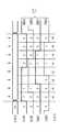
It is a block diagram which shows the structural example of a solid-state image sensor equipped with a parallel column ADC.
FIG. 19 is a diagram for explaining the operation of the circuit shown in FIG. 4; FIG.
20 is a diagram for explaining linearity.
21 is a diagram for explaining linearity.
FIG. 22 is a diagram for explaining the operation of the circuit shown in FIG. 4; FIG.
23 is a diagram for explaining linearity.
24 is a diagram for explaining the loss of monotone increaseability.
25 is a diagram for explaining switching of an operation mode.
FIG. 26 is a diagram for explaining the operation of the circuit shown in FIG. 4; FIG.
27 is a diagram for explaining linearity.
28 is a diagram for explaining an error.
FIG. 29 is a diagram for explaining the operation of the circuit shown in FIG. 4; FIG.
30 is a diagram for explaining linearity.
31 is a diagram for explaining an error.
32 is a diagram for explaining the improvement in monotone increaseability.
33 is a diagram for explaining the operation of the circuit shown in FIG.
34 is a diagram for explaining switching of an operation mode.
FIG. 35 shows details of a circuit for performing the operation shown in FIG. 33; FIG.
36A to 36C are views for explaining the operation of the circuit shown in FIG.
FIG. 37 shows another detail of the circuit shown in FIG. 3; FIG.
FIG. 38 shows details of the circuit shown in FIG. 37; FIG.
FIG. 39 is a view for explaining the operation of the circuit shown in FIG. 37; FIG.
40 is a diagram for explaining switching of an operation mode.
41 is a diagram for explaining a decode.
42 is a diagram for explaining linearity.
43 is a diagram for explaining linearity.
44 is a diagram for explaining switching of an operation mode.
45 is a diagram for explaining an error.
46 is a diagram for explaining linearity.
47 is a diagram for explaining a recording medium.
[제1의 실시의 형태에 관해][About 1st embodiment]
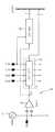
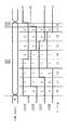
도 3에 A/D 변환 장치(Analog Digital Converter)의 한 실시의 형태의 구성을 도시한다. A/D 변환 장치(20)는, 참조 전압 공급부(21), 비교기(22), 래치 디코드 회로(23), 및 리플 카운터(24)를 갖는다. 래치 디코드 회로(23)는, 래치 회로와 디코드 회로로 구성된다.3 shows a configuration of an embodiment of an A / D converter (Analog Digital Converter). The A /
도 3에 도시한 A/D 변환 장치(20)는, 상위 비트 카운터와 위상이 다른 클록 신호를 래치와 디코드를 한 TDC(Time to Digital Converter)로 하위 비트의 정보를 얻는 적분형 A/D 변환 장치(20)이다. 여기서는 예로서, 상위 11bit의 리플 카운터와 하위 3bit의 TDC로 구성한 분해능 14bit의 A/D 변환 장치(20)를 나타낸다.The A /
비교기(22)는, 참조 전압 공급부(21)로부터 공급되는 시간과 함께 전압치가 선형으로 변화하는 램프 파형의 참조 전압(Vramp)과, 입력 전압(VSL)을 비교하고, 그 결과에 응한 레벨의 출력 신호(VCO)를 래치 디코드 회로(23)와 리플 카운터(24)에 출력한다.The
비교기(22)의 출력 신호(VCO)의 레벨이 반전한 때에, 리플 카운터(24)의 상위 비트는 카운트를 정지하고, 래치 디코드 회로(23)는 클록 신호(CLK)의 위상 정보를 래치하여, 래치 데이터(EB)(확장 코드(EB))를 출력한다. 래치 디코드 회로(23)에는, 위상이 45도씩 다른 클록 신호(CLKA), 클록 신호(CLKB), 클록 신호(CLKC), 클록 신호(CLKD)가 공급되고, 각각의 클록 신호에 의해 위상 정보가 래치된다.When the level of the output signal VCO of the
이러한 클록 신호들은, 공급부(도시 생략)로부터 공급되고, 공급부로부터 공급되는 클록 신호는, 제어부(도시 생략)의 제어에 의거하여, 래치 디코드 회로(23)에 공급된다. 후술하지만, 이들의 클록 신호는, 소정의 영역(예를 들면, 백 영역(white region))이라고 판단될 때에, 그 공급이 정지되는데, 그와 같은 판단은, 제어부에 의해 행하여진다.These clock signals are supplied from a supply unit (not shown), and the clock signal supplied from the supply unit is supplied to the
래치 디코드 회로(23)는, 래치 정보를 펄스(열(train))로 변환하고, 그 펄스를 리플 카운터(24)의 카운트 클록 신호로서 출력한다. 리플 카운터(24)는, 래치 디코드 회로(23)의 카운트 클록 신호에 응하여, 클록 신호의 위상 정보를 리플 카운터의 최하위 비트로서 바이너리 코드로 변환한다.The
도 4에, 도 3에 도시한 A/D 변환 장치(20)의 래치 디코드 회로(23)의 상세한 구성을 도시한다. 도 4에 도시한 래치 디코드 회로(23)는, 확장 코드를 바이너리값(binary value)으로 변환하는 회로이다. 도 4에 도시한 래치 디코드 회로(23)는, 래치 회로(41)와 디코드 회로(51)로 구성되고, 래치 회로(41)는, 플립플롭(42 내지 45)으로 구성되어 있다. 디코드 회로(51)는, 셀렉터(52), 제1의 디코드 회로(53), 제1의 리플 카운터부(54), 마스크 회로(55), 제2의 디코드 회로(56), 제2의 리플 카운터부(57)를 갖는다.FIG. 4 shows a detailed configuration of the
비교기(22)(도 3)는, 시간과 함께 전압치가 선형으로 변화하는 램프 파형의 참조 전압(Vramp)과 입력 전압(VSL)을 비교하고, 그 결과에 응한 레벨의 출력 신호(VCO)를 래치 회로(41)의 각 플립플롭(42 내지 45)에 출력한다.The comparator 22 (FIG. 3) compares the reference voltage Vramp and the input voltage VSL of the ramp waveform whose voltage value changes linearly with time, and latches the output signal VCO of the level corresponding to the result. Output to each
래치 회로(41)는, 제1의 래치로서의 플립플롭(42, 43, 44)을 가지며, 제2의 래치로서의 플립플롭(45)을 갖는다. 래치 회로(41)는, 위상이 다른 복수의 클록 신호를 이용하여 비교기(22)의 출력 신호(VCO)가 반전한 타이밍에서 위상 정보를 래치한다. 본 실시의 형태에서는, 위상이 다른 복수의 클록 신호로서, 클록 신호(CLKA)를 기준으로 위상이 45도씩 차례로 어긋난, 클록 신호(CLKB), 클록 신호(CLKC), 클록 신호(CLKD)와 클록 신호(CLKA) 자신을 포함한 4개의 클록 신호가 사용된다. 위상 어긋남의 45도는 클록 신호 주기(Tck)의 1/8에 상당한다.The
각각의 플립플롭(42 내지 45)은 각각, 비교기(22)의 출력 신호(VCO)에 동기하여, 클록 신호(CLKA), 클록 신호(CLKB), 클록 신호(CLKC), 클록 신호(CLKD)의 위상 정보를 래치한다. 플립플롭(42)은, 비교기(22)의 출력 신호(VCO)에 동기하여 클록 신호(CLKD)를 래치한다. 플립플롭(42)의 Q출력으로부터는 확장 코드(EB)[0]를 얻을 수 있고, 플립플롭(42)은 얻어진 확장 코드(EB)[0]를 셀렉터(52)에 출력한다.Each of the flip-
플립플롭(43)은, 비교기(22)의 출력 신호(VCO)에 동기하여 클록 신호(CLKC)의 위상 정보를 래치한다. 플립플롭(43)의 Q출력으로부터는 확장 코드(EB)[1]를 얻을 수 있고, 플립플롭(43)은 얻어진 확장 코드(EB)[1]를 셀렉터(52)에 출력한다. 플립플롭(44)은, 비교기(22)의 출력 신호(VCO)에 동기하여 클록 신호(CLKB)의 위상 정보를 래치한다. 플립플롭(44)의 Q출력으로부터는 확장 코드(EB)[2]를 얻을 수 있고, 플립플롭(44)은 얻어진 확장 코드(EB)[2]를 셀렉터(52)에 출력한다.The flip-
플립플롭(45)은, 비교기(22)의 출력 신호(VCO)에 동기하여 클록 신호(CLKA)의 위상 정보를 래치한다. 플립플롭(45)의 Q출력으로부터는 확장 코드(EB)[3]를 얻을 수 있고, 플립플롭(45)은 얻어진 확장 코드(EB)[3]를 제1의 디코드 회로(53)와 마스크 회로(55)에 출력한다.The flip-
셀렉터(52)는, 셀렉터 신호(EBSEL)[2:0]에 응하여, 플립플롭(42 내지 44)으로부터 출력되는 확장 코드(EB)[0], 확장 코드(EB)[1], 확장 코드(EB)[2]를 순차적으로 선택하고, 신호(EBO)로서 제1의 디코드 회로(53)에 출력한다. 제1의 디코드 회로(53)는, 래치 회로(41)의 래치 정보인 확장 코드(EB)[0] 내지 EB[2]를, 펄스 신호(EBCK)와 확장 코드[3]에 응하여 펄스(열)로 변환하고, 그 펄스 신호(EBCKO)를 제1의 리플 카운터부(54)의 카운트 클록 신호로서 출력한다.The
제1의 디코드 회로(53)는, 2개의 AND 회로와 1개의 OR 회로로 구성되는 AND-OR 회로(61)를 갖는다. AND-OR 회로(61)의 제1의 3입력 AND 회로의 제1의 입력단자는, 펄스 신호(EBCK)의 공급 라인에 접속되어 있다. 제1의 3입력 AND 회로의 제2의 부(negative)입력단자는, 확장 코드(EB)[3]의 출력 라인에 접속되고, 제3의 부입력단자는, 셀렉터(52)의 신호(EBO)의 공급 라인에 접속되어 있다.The
AND-OR 회로(61)의 제2의 3입력 AND 회로의 제1의 입력단자는, 펄스 신호(EBCKO)의 공급 라인에 접속되어 있다. 제2의 3입력 AND 회로의 제2의 입력단자는, 확장 코드(EB)[3]의 출력 라인에 접속되고, 제3의 입력단자는, 셀렉터(52)의 신호(EBO)의 공급 라인에 접속되어 있다. 제1의 3입력 AND 회로와 제2의 3입력 AND 회로로부터의 출력은, OR 회로에 각각 공급되는 구성으로 되어 있다. 그리고, OR 회로로부터의 출력은, 제1의 리플 카운터부(54)에 공급되는 구성으로 되어 있다.The first input terminal of the second three-input AND circuit of the AND-
제1의 리플 카운터부(54)는, 제1의 디코드 회로(53)의 카운트 클록 신호에 응하여, 클록 신호의 위상 정보를 하위 비트로서 바이너리 코드로 변환한다. 제1의 리플 카운터부(54)는, 기억 소자로서 종속 접속된 플립플롭(62)과 플립플롭(63)을 갖는다. 플립플롭(62)의 단자(CIN)는, 제1의 디코드 회로(53)의 펄스 신호(EBCKO)의 공급 라인에 접속되고, 입력(D)이 반전 출력(/Q)("/"은 반전을 나타낸다)에 접속되고, 출력(Q)이 플립플롭(63)의 단자(CIN)에 접속되어 있다. 플립플롭(63)의 D입력은, 반전 출력(/Q)에 접속되고, 출력(Q)이 제2의 디코드 회로(56)에 접속되어 있다.The
마스크 회로(55)는, 마스크 신호(XEBMSK)에 응하여 래치 회로(41)에 의한 확장 코드(EB)[3]를 제2의 디코드 회로(56)에 입력시키는지 비입력으로 하는지를 결정하고 처리한 마스크 처리를 행한다. 마스크 회로(55)는, 부입력의 2입력 AND 회로로 구성되어 있다. 마스크 회로(55)의 AND 회로의 제1의 부입력단자는, 래치 회로(41)의 확장 코드(EB)[3]의 공급 라인에 접속되고, 제2의 부입력단자는, 액티브 레벨이 로우 레벨인 마스크 신호(XEBMSK)의 공급 라인에 접속되어 있다.The
제2의 디코드 회로(56)는, 래치 회로(41)의 확장 코드(EB)[3]를, 펄스 신호(EB4CK)에 응하여 펄스(열)로 변환하고, 그 신호(Q)[2]를 제2의 리플 카운터부(57)의 카운트 클록 신호로서 출력한다.The
제2의 디코드 회로(56)는, 2개의 AND 회로와 1개의 OR 회로로 구성되는 AND-OR 회로(64)를 갖는다. AND-OR 회로(64)의 제1의 2입력 AND 회로의 제1의 입력단자는, 펄스 신호(EB4CK)의 공급 라인에 접속되고, 제2의 입력단자는, 마스크 회로(55)의 출력 단자에 접속되어 있다. AND-OR 회로(64)의 제2의 2입력 AND 회로의 제1의 부입력단자는, 마스크 회로(55)의 출력 단자에 접속되고, 제2의 입력단자는, 제1의 리플 카운터부(54)의 출력 Q[1]의 출력 라인에 접속되어 있다. 제1의 2입력 AND 회로의 출력과 제2의 AND 회로의 출력은, OR 회로에 공급되고, OR 회로로부터의 출력 신호(Q)[2]는, 제2의 리플 카운터부(57)에 공급되도록 구성되어 있다.The
제2의 리플 카운터부(57)는, 제2의 디코드 회로(56)의 카운트 클록 신호에 응하여, 클록 신호의 위상 정보를 리플 카운터의 상위 비트로서 바이너리 코드로 변환한다. 제2의 리플 카운터부(57)는, 플립플롭(57) 및 리플 카운터(24)(도 3)를 갖는다. 플립플롭(57)은, 입력(D)이 반전 출력(/Q)("/"은 반전을 나타낸다)에 접속되고, 단자(CIN)가 제2의 디코드 회로(56)의 출력 신호(Q)[2]의 공급 라인에 접속되고, 출력(Q)이 리플 카운터(24)(도 3)의 입력단자에 접속되어 있다. 플립플롭(57)은, 바이너리 변환 후의 기억 소자(래치)로서 기능한다.In response to the count clock signal of the
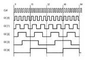
도 5에, 도 4의 A/D 변환 장치(20)의 동작을 설명하기 위한 타이밍 차트를 도시하고, 도 6에, 확장 코드를 바이너리값으로 변환하는 알고리즘을 도시하고, 도 7에, 확장 코드(EB)[3:0]를 바이너리값으로 디코드한 결과의 예를 도시한다.FIG. 5 shows a timing chart for explaining the operation of the A /
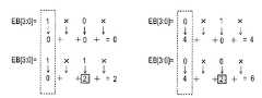
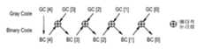
도 5에서는 1/8Tck(Tck는 클록 신호 주기)씩 위상이 어긋난 4개의 클록 신호의 경우에 관해 나타내고 있다. 4개의 클록 신호(CLKA 내지 CLKD)의 0/1의 조합에 의해, 클록 신호의 주기가 8등분되어 있다. 최초의 0 내지 1/8Tck의 기간에서는 클록 신호(CLK)[3:0]=1000b, 다음의 1/8Tck 내지 2/8Tck의 기간에서는 클록 신호(CLK)[3:0]=1100b, …가 된다. 클록 신호(CLK)의 위상을 8분할함으르써, 바이너리 코드로 3b분량의 정보를 얻을 수 있다.In FIG. 5, the case of four clock signals which shifted phase by 1/8 Tck (Tck is a clock signal period) is shown. The cycle of the clock signal is divided into eight parts by the combination of 0/1 of the four clock signals CLKA to CLKD. Clock signal CLK [3: 0] = 1000b in the period of the first 0 to 1 / 8Tck, clock signal CLK [3: 0] = 1100b in the period of the next 1 / 8Tck to 2 / 8Tck; . By dividing the phase of the clock signal CLK by eight, 3b information can be obtained by binary code.
비교기(22)의 출력 신호(VCO)가 하이 레벨(H)로부터 로우 레벨(L)로 변화하는 순간에 클록 신호(CLK)[3:0]가 래치되고, 래치 데이터를 확장 코드(EB)[3:0]로 한다. 클록 신호의 최초의 0 내지 1/8Tck의 기간을 "0", 1/8Tck 내지 2/8Tck의 기간을 "1", 이후 2, 3, 4 …라는 카운트값으로 변환하는 것으로 하면, 도 7에 도시하는 바와 같은 대응 관계의 수의 펄스를 발생시킨다.The clock signal CLK [3: 0] is latched at the moment when the output signal VCO of the
3bit TDC에서는, 확장 코드(EB)[3]=1인 경우는, 확장 코드(EB)[2:0]의 "1"인 수, 확장 코드(EB)[3]=0인 경우는, 확장 코드(EB)[2:0]의 "0"인 수와 그것에 4를 더한 수가 대응하는 수치가 된다. 이와 같은 알고리즘에 의하면, 도 7을 참조하면, 확장 코드(EB)[3], EB[2], EB[1], EB[0]가, "1, 0, 0, 0"인 경우, 그 바이너리 코드는, "000"이 되고, 디코드값은 "0"이 된다. 마찬가지로, 확장 코드(EB)[3], EB[2], EB[1], EB[0]가, "1, 1, 0, 0"인 경우, 그 바이너리 코드는, "001"이 되고, 디코드값은 "1"이 된다.In the 3-bit TDC, when the extension code EB [3] = 1, the number of extension codes EB [2: 0] is "1", and when the extension code EB [3] = 0, the extension is performed. The number "0" of the code EB [2: 0] and the number plus 4 are the corresponding numerical values. According to such an algorithm, referring to FIG. 7, when the extension codes EB [3], EB [2], EB [1], and EB [0] are “1, 0, 0, 0”, The binary code is "000" and the decode value is "0". Similarly, when the extension codes EB [3], EB [2], EB [1], and EB [0] are “1, 1, 0, 0”, the binary code is “001”, The decode value is "1".
확장 코드(EB)[3], EB[2], EB[1], EB[0]가, "1, 1, 1, 0"인 경우, 그 바이너리 코드는, "010"이 되고, 디코드값은 "2"가 된다. 확장 코드(EB)[3], EB[2], EB[1], EB[0]가, "1, 1, 1, 1"인 경우, 그 바이너리 코드는, "011"이 되고, 디코드값은 "3"이 된다. 확장 코드(EB)[3], EB[2], EB[1], EB[0]가, "0, 1, 1, 1"인 경우, 그 바이너리 코드는, "100"이 되고, 디코드값은 "4"가 된다.When the extension codes EB [3], EB [2], EB [1], and EB [0] are "1, 1, 1, 0", the binary code is "010" and the decode value Becomes "2". When the extension codes EB [3], EB [2], EB [1], and EB [0] are "1, 1, 1, 1", the binary code is "011" and the decode value Becomes "3". When the extension codes EB [3], EB [2], EB [1], and EB [0] are "0, 1, 1, 1", the binary code is "100" and the decode value Becomes "4".
확장 코드(EB)[3], EB[2], EB[1], EB[0]가, "0, 0, 1, 1"인 경우, 그 바이너리 코드는, "101"이 되고, 디코드값은 "5"가 된다. 마찬가지로, 확장 코드(EB)[3], EB[2], EB[1], EB[0]가, "0, 0, 0, 1"인 경우, 그 바이너리 코드는, "110"이 되고, 디코드값은 "6"이 된다. 확장 코드(EB)[3], EB[2], EB[1], EB[0]가, "0, 0, 0, 0"인 경우, 그 바이너리 코드는, "111"이 되고, 디코드값은 "7"이 된다. 이와 같이 하여, 확장 코드가 디코드값으로 변환된다.When the extension codes EB [3], EB [2], EB [1], and EB [0] are "0, 0, 1, 1", the binary code is "101", and the decode value Becomes "5". Similarly, when the extension codes EB [3], EB [2], EB [1], and EB [0] are “0, 0, 0, 1”, the binary code is “110”. The decode value is "6". When the extension code (EB) [3], EB [2], EB [1], or EB [0] is "0, 0, 0, 0", the binary code is "111" and the decode value. Becomes "7". In this way, the extension code is converted into a decoded value.
[소비 전력을 저감시키기 위한 처리에 관해][Process for Reducing Power Consumption]
이와 같이 A/D 변환 회로(20)는 동작하기 때문에, 확장 코드에 의한 분해능을 높인 A/D 변환을 행하는 것이 가능해진다. 예를 들면, 이와 같은 A/D 변환 회로(20)를 구비하는 디지털 카메라에 의하면, 분해능이 높음에 의한 화질의 향상을 기대할 수 있다. 즉, 분해능이 높아짐에 의해, 이와 같은 A/D 변환 회로(20)를 구비한 장치에서의 데이터의 질, 예를 들면, 화질이나 음질을 높이는 것이 가능해진다. 이하의 설명에서는, 주로, 디지털 카메라 등의 화상이나 영상을 취급하는 장치에 본 실시의 형태에서의 A/D 변환 회로가 적용된 경우를 예로 들어, 화질이 저하되는 일 없이, 소비 전력을 저하시키기 위한 처리에 관해 설명한다.Thus, since the A /
상기한 바와 같이, 래치 디코드 회로(23)에는, 4개의 클록 신호가 입력된다. 이 클록 신호를 정지함으로써, 소비 전력을 저감시킬 수 있다. 그러나, 클록 신호를 정지하면, 분해능이 낮아진다. 그래서, 클록 신호가 정지하고, 분해능이 저하되었다고 하여도, 그 영향이 거의 없는(무시할 수 있는) 조건에 관해 설명한다.As described above, four clock signals are input to the
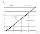
도 8은 이미지 센서에 입사하는 광의 조도와, 그때에 이미지 센서의 화소 내에 발생하는 전자수의 관계를 도시한 그래프이다. 저조도, 즉 흑 영역에서는 고정 성분인 회로 노이즈가 지배적이고, 또한 광량에 비례하는 신호 성분도 작다. 한편, 고조도, 즉 백 영역에서는 조도의 제곱근에 비례한 광 숏 노이즈(light shot noise)가 지배적이다.8 is a graph showing the relationship between the illuminance of light incident on the image sensor and the number of electrons generated in the pixel of the image sensor at that time. In low light, that is, in the black region, circuit noise, which is a fixed component, is dominant, and signal components proportional to the amount of light are small. On the other hand, in the high illumination, that is, the back region, light shot noise proportional to the square root of the illumination is dominant.
입사광에 의해 발생하는 전자의 수를 Q[e-]로 하면, 광 숏 노이즈는 다음의 식(1)으로 정의된다.If the number of electrons generated by the incident light is Q [e-], the optical shot noise is defined by the following equation (1).

전압 신호에의 변환 효율을 E[V/e-]로 하면, 광 숏 노이즈는 다음의 식(2)으로 표시된다.When the conversion efficiency to the voltage signal is set to E [V / e-], the optical short noise is expressed by the following equation (2).

여기서, 판독 회로에 기인하는 고정 성분의 회로 노이즈를 Nc[Vrms]로 하고, 노이즈의 총량 N[Vrms]을, 전자의 수(Q)의 함수로서 표시하면, 다음의 식(3)이 되고, 다음의 식(4)이 된다.Here, suppose that the circuit noise of the fixed component caused by the readout circuit is Nc [Vrms ], and the total amount of noise N [Vrms ] is expressed as a function of the number of electrons (Q). And the following equation (4).

도 9에 도시한 그래프는, 횡축을 광전자수 Q[e-]이고, 종축을 노이즈의 총량 N[Vrms]으로 한 때의 관계를 도시한 그래프이다. 도 9중, QFD[e-]는, 화소의 포화 용량이다. 또한, 이미지 센서의 다이내믹 레인지를 DRANGE[V]로 하고, A/D 변환 장치의 분해능을 n[bit]로 한다. 이와 같은 경우, 1LSB(least significant bit)의 무게, 즉 1LSB에서 변화하는 전압폭은 다음의 식(5)으로 표시된다.The graph shown in FIG. 9 is a graph showing the relationship when the horizontal axis is the photoelectron number Q [e-] and the vertical axis is the total amount of noise N [Vrms ]. In FIG. 9, QFD [e-] is a saturation capacitance of a pixel. In addition, the dynamic range of the image sensor is set to DRANGE [V], and the resolution of the A / D converter is set to n [bit]. In this case, the weight of the least significant bit (1 LSB), that is, the voltage width changing in the 1 LSB, is expressed by the following equation (5).

도 9에는, 노이즈의 총량(N)의 곡선과, 그 잡음의 총량(N)의 반분의 노이즈의 총량((1/2)N)의 곡선을 도시하고 있다. 여기서, 노이즈의 총량의 반분인 N/2보다 1LSB의 전압폭(DRANGE/2n)이 작은 경우, 1LSB의 변화는 노이즈에 묻히고, 그 영역(예를 들면, 백 영역)에서, A/D 변환 장치의 분해능은 반드시 n[bit]일 필요는 없다. 이와 같은 노이즈에 묻혀 버리는 영역에서, 화질을 유지하기 위해 분해능을 유지할 필요성은 없고, n비트 이하의 분해능이라도 좋다고 생각된다.Fig. 9 shows a curve of the total amount N of noise and a curve of the total amount ((1/2) N) of half of the total amount N of the noise. Here, when the voltage width (DRANGE / 2n ) of 1LSB is smaller than N / 2 which is half of the total amount of noise, the change of 1LSB is buried in the noise, and in the area (for example, the back area), A / D The resolution of the converter does not necessarily need to be n [bit]. In the area where such noise is buried, it is not necessary to maintain the resolution in order to maintain the image quality, and it is considered that resolution of n bits or less may be sufficient.
상기한 바와 같이, A/D 변환 회로(20)는, 래치 디코드 회로(23)에 4개의 클록 신호를 입력하고, 처리함으로써, 하위 3비트를 만들어 내어, 분해능을 높이고 있지만, 이 클록 신호를, 화질에 영향을 주지 않는 범위에서 정지시킴으로써, A/D 변환 회로(20)의 소비 전력을 저하시킬 수 있다. 환언하면, 고조도의 부분, 예를 들면 백 영역에서 A/D 변환 장치(20)의 최고의 분해능이 필요하지 않는 영역이 있는 것에 착안하여, 이 영역에서의 A/D 변환 장치(20)의 분해능을 떨어뜨림으로써 A/D 변환 장치(20) 전체의 저소비 전력화를 실현한다.As described above, the A /
또한, 노이즈에 묻혀 버리는 조건에 관해, 화질 평가 등을 거쳐서 정해지는 것이고 반드시, 상기한 조건으로 한정되는 것은 아니다. 즉, 상기한 예에서는, 노이즈의 총량의 절반 분인 N/2보다 1LSB의 전압폭(DRANGE/2n)이 작은 경우로 하였지만, 노이즈의 총량의 절반 분이 아니라, 그 밖의 값, 예를 들면 3분의 1이나 5분의 1인 값이라도 좋다.In addition, the conditions buried in the noise are determined through image quality evaluation and the like, and are not necessarily limited to the above conditions. That is, in the above example, the voltage width (DRANGE / 2n ) of 1LSB is smaller than N / 2, which is half of the total amount of noise, but other values, such as 3, are not half of the total amount of noise. The value may be one half or one fifth.
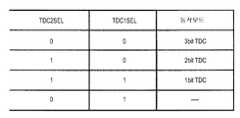
A/D 변환 회로(20)에서 래치 디코드 회로(23)에 입력되는 클록 신호를 정지시킨 경우의 디코드값에 관해 설명한다. 상기한 도 5 내지 7을 참조하여, 클록 신호를 정지시키지 않는 때의 디코드값, 즉 3개의 바이너리 코드가 얻어지는 3bit TDC로서 동작하는 동작 모드일 때의 디코드값에 관해 설명하였다. 마찬가지로, 이하에, 2개의 클록 신호를 정지시킴에 의해, 2개의 바이너리 코드가 얻어지는 2bit TDC로서 동작하는 동작 모드일 때의 디코드값과, 3개의 클록 신호를 정지시킴에 의해 하나의 바이너리 코드가 얻어지는 1bit TDC로서 동작하는 동작 모드로서 기능한 때의 디코드값에 관해 각각 설명한다.The decode value when the clock signal input to the
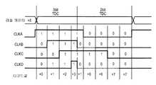
[2bit TDC의 동작 모드시에 관해][In operation mode of 2bit TDC]
도 10에, 도 4의 A/D 변환 장치(20)의 동작을 설명하기 위한 타이밍 차트로서, 래치 디코드 회로(23)에 입력된 4개의 클록 신호중의 2개의 클록 신호를 정지시킨 때이고, 2bit TDC로서 기능한 때의 타이밍 차트를 도시한다. 도 11에, 그 때의 확장 코드를 바이너리값으로 변환하는 알고리즘을 도시한다. 도 12에, 그 때의 확장 코드(EB)[3:0]를 바이너리값으로 디코드한 결과의 예를 도시한다.FIG. 10 is a timing chart for explaining the operation of the A /
래치 디코드 회로(23)에는, 1/8Tck(Tck는 클록 신호 주기)씩 위상이 어긋난 4개의 클록 신호가 입력되는데, 그 중의 2개의 클록 신호가 동작하고 있을 때의 타이밍 차트이다. 도 10에는, 클록 신호(CLKA)와 클록 신호(CLKC)가 동작하고, 클록 신호(CLKB)와 클록 신호(CLKD)가 정지되어 있는 상태일 때의 타이밍 차트를 도시한다. 또한 도 10에서, 점선은, 클록 신호가 정지되어 있는 것을 나타낸다.Four clock signals that are out of phase by 1/8 Tck (Tck is a clock signal period) are input to the
2bit TDC의 동작 모드에서는, EB[3] 그 자체가 1인 경우는 0카운트가 되고, 0인 경우는 4카운트되고, EB[1]은, EB[3]가 1일 때는 논리값 "1"의 수를, 0일 때는 논리값 "0"의 수를 각각 2카운트한다. 즉, 확장 코드(EB)[3]=1인 경우는, 확장 코드(EB)[1 :0]의 "1"인 수, 확장 코드(EB)[3]=0인 경우는, 확장 코드(EB)[1 :0]의 "0"인 수와 그것에 4를 더한 수가 대응하는 수치가 된다.In the 2-bit TDC operating mode, if EB [3] itself is 1, it is 0 counts; if it is 0, it is 4 counts; EB [1] is logical value "1" when EB [3] is 1; If the number is 0, the number of logical values " 0 " That is, when the extension code EB [3] = 1, the number that is "1" of the extension code EB [1: 0], and when the extension code EB [3] = 0, the extension code ( The number "0" of EB) [1: 0] and the number plus 4 are the corresponding numerical values.
이와 같은 알고리즘에 의하면, 클록 신호 주기의 최초의 0 내지 2/8Tck의 기간을 "0", 3/8Tck 내지 4/8Tck의 기간을 "2", 5/8Tck 내지 6/8Tck의 기간을 "4", 7/8Tck 내지 8/8Tck의 기간을 "6"이라는 카운트값으로 변환되고, 도 12에 도시하는 바와 같은 대응 관계의 수의 펄스가 발생된다.According to this algorithm, the period of the first 0 to 2 / 8Tck of the clock signal period is "0", the period of 3 / 8Tck to 4 / 8Tck is "2", and the period of 5 / 8Tck to 6 / 8Tck is "4". ", The period of 7 / 8Tck to 8 / 8Tck is converted into the count value" 6 ", and the pulse of the number of correspondences as shown in FIG. 12 is generated.
확장 코드(EB)[3], EB[1]가, "1, 0"인 경우, 그 바이너리 코드는, "000"이 되고, 디코드값은 "0"이 된다. 확장 코드(EB)[3], EB[1]가, "1, 1"인 경우, 그 바이너리 코드는, "010"이 되고, 디코드값은 "2"가 된다. 확장 코드(EB)[3], EB[1]가, "0, 1"인 경우, 그 바이너리 코드는, "100"이 되고, 디코드값은 "4"가 된다. 확장 코드(EB)[3], EB[1]가, "0, 0"인 경우, 그 바이너리 코드는, "110"이 되고, 디코드값은 "6"이 된다.When the extension codes EB [3] and EB [1] are "1, 0", the binary code is "000" and the decode value is "0". When the extension codes EB [3] and EB [1] are "1, 1", the binary code is "010" and the decode value is "2". When the extension codes EB [3] and EB [1] are "0, 1", the binary code is "100" and the decode value is "4". When the extension codes EB [3] and EB [1] are "0, 0", the binary code is "110" and the decode value is "6".
이와 같은 경우, 클록 신호의 1주기의 중에서, 출력 신호(VCO)가 변화하는 타이밍에서, 위상이 90도씩 다른 2개의 클록 신호(CLKA, CLKC)의 값을 래치하게 되고, 4가지의 확장 코드(EB)[3], EB[1]를 얻을 수 있게 된다. 이 4가지의 코드를 디코드하여 2bit의 하위 비트의 정보를 얻을 수 있고, 이것을 도시하면, 도 12에 도시한 바와 같이 된다.In such a case, at the timing at which the output signal VCO changes in one cycle of the clock signal, the values of the two clock signals CLKA and CLKC having different phases by 90 degrees are latched, and four extension codes ( EB) [3] and EB [1] can be obtained. The four codes can be decoded to obtain 2 bits of low-order information, which is shown in FIG.
여기서, 3bit TDC와 비교하면 위상 정보의 취득에 필요한 클록 신호의 갯수가 2개 적은 것을 알 수 있다. 이것은 1bit의 분해능을 떨어뜨림에 의해, 2개의 클록 신호를 동작시킬 필요가 없어지는 것을 의미한다. 2개의 클록 신호를 동작시키지 않으면, 그 만큼, 소비되는 전력을 삭감할 수 있음은 분명하다.Here, it can be seen that the number of clock signals required for acquiring phase information is smaller than that of 3 bit TDC. This means that by reducing the resolution of 1 bit, there is no need to operate two clock signals. If the two clock signals are not operated, it is obvious that power consumption can be reduced by that amount.
[1bit TDC의 동작 모드에 관해][Operation Mode of 1bit TDC]
도 13에, 도 4의 A/D 변환 장치(20)의 동작을 설명하기 위한 타이밍 차트로서, 래치 디코드 회로(23)에 입력되는 4개의 클록 신호중의 3개의 클록 신호를 정지시킨 때이고, 1bit TDC로서 기능한 때의 타이밍 차트를 도시한다. 도 14에, 그 때의 확장 코드를 바이너리값으로 변환하는 알고리즘을 도시한다. 도 15에, 그 때의 확장 코드(EB)[3:0]를 바이너리값으로 디코드한 결과의 예를 도시한다.FIG. 13 is a timing chart for explaining the operation of the A /
래치 디코드 회로(23)에는, 1/8Tck(Tck는 클록 신호 주기)씩 위상이 어긋난 4개의 클록 신호가 입력되는데, 그중의 하나의 클록 신호가 동작하고 있을 때의 타이밍 차트이다. 도 13에는, 클록 신호(CLKA)가 동작하고, 클록 신호(CLKB), 클록 신호(CLKC), 및 클록 신호(CLKD)가 정지되어 있는 상태일 때의 타이밍 차트를 도시한다. 또한 도 13에서, 점선은, 클록 신호가 정지되어 있는 것을 나타낸다.Four clock signals that are out of phase by 1/8 Tck (Tck is a clock signal period) are input to the
1bit TDC의 동작 모드에서는, EB[3] 그 자체가 "1"인 경우는 "0"카운트가 되고, "0"인 경우는 "4"카운트된다. 즉, 확장 코드(EB)[3]=1인 경우는, "0"이 되고, 확장 코드(EB)[3]=0인 경우는, "4"가 된다.In the operation mode of 1-bit TDC, when EB [3] itself is "1", it counts as "0", and when it is "0", it counts as "4". That is, when extension code EB [3] = 1, it is "0", and when extension code EB [3] = 0, it is "4".
이와 같은 알고리즘에 의하면, 클록 신호 주기의 최초의 0 내지 4/8Tck의 기간을 "0", 5/8Tck 내지/8Tck의 기간을 "4"라는 카운트값으로 변환되고, 도 15에 도시하는 바와 같은 대응 관계의 수의 펄스를 발생한다. 확장 코드(EB)[3]가, "1"인 경우, 그 바이너리 코드는, "000"이 되고, 디코드값은 "0"이 된다. 확장 코드(EB)[3]가, "0"인 경우, 그 바이너리 코드는, "100"이 되고, 디코드값은 "4"가 된다.According to this algorithm, the period of the first 0 to 4 / 8Tck of the clock signal period is converted into a count value of "0" and the period of 5 / 8Tck to / 8Tck is "4", as shown in FIG. Generate pulses of the number of corresponding relationships. When the extension code EB [3] is "1", the binary code is "000" and the decode value is "0". When the extension code EB [3] is "0", the binary code is "100" and the decode value is "4".
이와 같은 경우, 필요한 클록 신호는 하나의 클록 신호(CLKA)만으로, 클록 신호의 Hi와 Lo의 2가지를 위상 정보로 하여 확장 코드(EB)[3]를 얻을 수 있다. 이 2가지의 코드를 디코드하여 1bit의 하위 비트의 정보를 얻을 수 있다.In such a case, the necessary clock signal is only one clock signal CLKA, and the extension code EB [3] can be obtained by using Hi and Lo of the clock signal as phase information. By decoding these two codes, one bit of lower bit information can be obtained.
여기서, 2bit TDC와 비교하면 위상 정보의 취득에 필요한 클록 신호의 갯수를 1개 줄일 수 있음을 알 수 있다. 또한 3bit TDC와 비교하면 위상 정보의 취득에 필요한 클록 신호의 갯수를 3개 줄일 수 있음을 알 수 있다. 3개의 클록 신호를 동작시키지 않으면, 그 만큼, 소비되는 전력을 삭감할 수 있음은 분명하다.Here, it can be seen that the number of clock signals required for acquiring phase information can be reduced by one compared with 2 bit TDC. In addition, it can be seen that the number of clock signals required for acquiring phase information can be reduced by three compared with 3bit TDC. If three clock signals are not operated, it is clear that the consumed power can be reduced by that amount.
이와 같이, 클록 신호를 정지시킴으로써, 분해능은 떨어지게 되지만, 클록 신호를 정지시키는 타이밍을 적절하게 행함으로써, 분해능의 저하에 의해 화질이 열화되는 일 없이, 소비 전력을 저감시키는 것이 가능해진다. 클록 신호를 정지시키는 타이밍은, 상기한 바와 같이, 예를 들면, 노이즈의 총량의 절반 분인 N/2보다 1LSB의 전압폭(DRANGE/2n)이 작아질 때이고, 이와 같은 영역에서 클록 신호를 정지시켜서, 분해능을 저하시켰다고 하여도, 실질적으로는 화질에 영향을 주는 일 없이, 디코드할 수 있게 된다.In this way, by stopping the clock signal, the resolution decreases, but by appropriately timing the clock signal to stop, it is possible to reduce power consumption without deteriorating the image quality due to the degradation of the resolution. As described above, the timing for stopping the clock signal is, for example, when the voltage width (DRANGE / 2n ) of 1LSB is smaller than N / 2, which is half of the total amount of noise, and the clock signal is removed in such an area. Even if it stops and the resolution is reduced, it becomes possible to decode without substantially affecting image quality.
[동작 모드의 전환에 관해][Switching to Operation Mode]
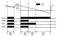
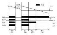
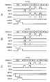
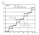
래치 디코드 회로(23)를, 3bit TDC, 2bit TDC, 1bit TDC의 순서로 전환하여 이용하는 경우, 환언하면, 4개의 클록 신호를 동작시키는 동작 모드로부터, 2개의 클록 신호를 동작시키는 동작 모드로 전환, 다시 하나의 클록 신호를 동작시키는 동작 모드로 전환하여 이용하는 경우에 관해, 도 16을 참조하여 설명한다.In the case where the
도 16에, A/D 변환 기간과 4개의 클록 신호의 동작 기간을 도시한다. A/D 변환 기간의 전반에는, 화소 출력(VSL)의 전위가 높은 전위(저조도)에서 계수(counting)가 실행되고, 후반에는 화소 출력(VSL)의 전위가 낮은 전위(고조도)에서 계수가 실행된다. A/D 변환 기간에서, 저조도의 흑 영역에서는 분해능이 높은 3bit TDC로 동작시키고, 그 때의 클록 신호는, 클록 신호(CLKA, CLKB, CLKC, CLKD)의 4개를 동작시켜 둔다. 그리고 분해능을 떨어뜨려도 좋은 영역에서, 2개의 클록 신호(CLKB, CLKD)를 정지시켜서, 2bit TDC로 동작시킨다. 또한, 하나의 클록 신호(CLKC)를 정지시켜서, 1bit TDC로 동작시킨다.16 shows an A / D conversion period and an operation period of four clock signals. In the first half of the A / D conversion period, counting is performed at a potential (low illuminance) of which the potential of the pixel output VSL is high, and in the second half, a coefficient is produced at a potential (high intensity) of which the potential of the pixel output VSL is low. Is executed. In the A / D conversion period, a low resolution black region is operated with a
이와 같이 순차적으로 클록 신호를 정지시킴에 의해, 항상 클록 신호를 4개 동작시켜서, m비트의 분해능으로 기능하고 있을 때와 비교하여, 클록 신호(CLKB, CLKC, CLKD)를 정지시켜서, n비트의 분해능으로 기능하고 있을 때의 쪽이, 정지시키고 있는 클록 신호의 분만큼 적어도 소비 전류를 삭감할 수 있다. 그리고, 클록 신호의 정지는, 백 영역에서 행하도록 함으로써, 클록 신호를 정지시켜서, 분해능을 떨어뜨렸다고 하여도, 실시적인 화질의 저하를 초래하는 일은 없다.By stopping the clock signals sequentially in this way, the clock signals are always operated by four clock signals, and the clock signals CLKB, CLKC, CLKD are stopped compared to when the clock signal is functioning with m bits of resolution. When it is functioning at a resolution, the current consumption can be reduced at least by the amount of the clock signal stopped. When the clock signal is stopped in the back region, the clock signal is stopped and the resolution is not reduced even if the resolution is decreased.
[클록 정지에 의한 부적합의 가능성에 관해][Possibility of nonconformity by clock stop]
그러나, 이와 같이 클록 신호를 순차적으로 정지시킴에 의해, 리니어리티가 악화되고, 단조증가성이 소실할 가능성이 있다. 그 이유를 설명하기 전에, A/D 변환 회로(20)에 공급되는 제어 신호에 관해 설명을 가한다. 도 17에, 제어 신호의 파형을 도시한다. 도 17A는, 래치 디코드 회로(23)가, 3bit TDC로서 기능하고 있을 때의 파형이고, 도 17B는, 2bit TDC로서 기능하고 있을 때의 파형이고, 도 17C는, 1bit TDC로서 기능하고 있을 때의 파형이다.However, by stopping the clock signals sequentially in this manner, there is a possibility that linearity deteriorates and monotonic increaseability is lost. Before explaining the reason, the control signal supplied to the A /
제어 신호(EBCK)의 펄스는 카운터를 구동하기 위한 신호원이다. 제어 신호(EBCKO)는, 제어 신호(EBCK)의 펄스를 통과시키는지의 여부를 나타내는 펄스이고, 확장 코드의 값의 조합에 의해 카운트가 필요한 경우는 펄스를 통과시키고, 카운트가 필요하지 않은 경우는 통과시키지 않도록 제어하기 위한 펄스이다. 통과한 펄스가, 실제로 카운트 클록 신호로서 카운터를 구동시킨다. 제어 신호(XEBMSK)는, 래치 회로(41)에 의한 확장 코드(EB)[3]를, 제2의 디코드 회로(56)에 입력시키는지 비입력으로 하는지를 결정하는 마스크 처리를 행하게 하기 위한 제어 신호이다. 제어 신호(EB4CK)는, 래치 회로(41)의 확장 코드(EB)[3]를, 제어 신호(EB4CK)의 펄스에 응하여 펄스(열)로 변환시켜서, 그 신호 D[2]를 제2의 리플 카운터부(28)의 카운트 클록 신호로서 출력시키기 위한 제어 신호이다.The pulse of the control signal EBCK is a signal source for driving the counter. The control signal EBCKO is a pulse indicating whether or not the pulse of the control signal EBCK is passed. If a count is required by the combination of the values of the extension codes, the pulse is passed. If the count is not necessary, the control signal EBCKO passes. It is a pulse to control not to make it. The pulse that passed actually drives the counter as a count clock signal. The control signal XEBMSK is a control signal for causing a mask process for determining whether the extension code EB [3] by the
도 17A 내지 도 17C에서, EB[3] 그 자체가 "1"인 경우, "0"카운트가 되고, EB[3] 그 자체가 "0"인 경우, "4"카운트가 되기 때문에, EB[3]은, 제어 신호(XEBMSK)와 제어 신호(EB4CK)로, 직접 3bit째의 리플 카운터(출력이 Q[2]의 플립플롭(57))에 제어 펄스가 보내진다.17A to 17C, when EB [3] itself is "1", it becomes "0" count, and when EB [3] itself is "0", it becomes "4" count, so that EB [ 3] is a control signal XEBMSK and a control signal EB4CK, in which control pulses are sent directly to the third-bit ripple counter (the output is flip-
3bit TDC일 때에는, EB[2:0]에 관해, EBSEL[2:0]로 각각의 확장 코드를 기억하는 플립플롭(62, 63)에 액세스되고, 그와 같은 타이밍에서 제어 신호(EBCK)가, 클록 신호 펄스를 하나씩 발생시킨다. EB[3]의 값과 액세스된 EB[2:0]의 값에 의해, 제어 신호(EBCKO)의 펄스를 통과시키는지, 또는 시키지 않는지에 의해 논리값의 수가, 1 또는 2비트째의 리플 카운터(출력이 Q[0], Q[1]의 플립플롭(62, 63))에 전해진다.In the case of a 3-bit TDC, flip-
도 17B에 도시하는 바와 같이, 2bit TDC일 때에는, EB[1]의 논리값이 2카운트되기 때문에, EBSEL[1]에 의한 EB[1]의 액세스가 2회 행하여짐에 의해, 2카운트된다. 도 17C에 도시하는 바와 같이, 1bit TDC에서는 EBSEL[2:0]에 의한 EB[2:0]에의 액세스는 없다.As shown in Fig. 17B, in the case of a 2-bit TDC, since the logic value of EB [1] is counted twice, the access of EB [1] by EBSEL [1] is performed twice, so that it is counted twice. As shown in Fig. 17C, in 1-bit TDC, there is no access to EB [2: 0] by EBSEL [2: 0].
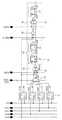
이와 같은 제어 신호에 의해 동작하는 도 4에 도시한 A/D 변환 회로(20)를 열병렬로 갖는 이미지 센서에 적용한 경우, 예를 들면, 도 18에 도시하는 바와 같이 적용한 경우, 제어 신호(EBSEL, EBCK, EB4CK, XEBMSK) 등은 전 칼럼에 공통으로 분배되는 제어 신호이다. 도 18은, 도 4에 도시한 A/D 변환 회로(20)를 열병렬로 갖는 이미지 센서에 적용한, 열병렬 ADC 탑재 고체 촬상 소자(CMOS 이미지 센서)의 구성례를 도시하는 블록도이다.In the case where the A /
도 18에 도시한 고체 촬상 소자(100)는, 화소부(102), 수직 주사 회로(103), 수평 전송 주사 회로(104), 및 ADC군으로 이루어지는 칼럼 처리 회로군(105)을 갖는다. 또한, 고체 촬상 소자(100)는, 디지털-아날로그 변환 장치(DAC)(106), 및 앰프 회로(107)를 갖는다. DAC(106)는, 도 3에서의 참조 전압 공급부(21)에 대응한다. 화소부(102)는, 포토 다이오드(광전 변환 소자)와 화소내 앰프를 포함하는 단위 화소(121)가 매트릭스형상(행렬형상)으로 배치되어 구성된다.The solid-
칼럼 처리 회로군(105)은, 열마다 ADC를 형성하는 칼럼 처리 회로(151)가 복수열 배열되어 있다. 각 칼럼 처리 회로(ADC)(151)는, 도 3, 도 4에서의 A/D 변환 회로(20)에 대응한다. 각 칼럼 처리 회로(151)는, DAC(106)에 의해 생성되는 참조 신호를 계단형상으로 변화시킨 램프 파형인 참조 신호(RAMP)(참조 전압(Vramp))와, 행선마다 화소로부터 수직 신호선(108)을 경유하여 얻어지는 아날로그 신호를 비교하는 비교기(151-1)를 갖는다. 이 비교기(151-1)는, 도 3에서의 비교기(22)에 대응한다.In the column
또한, 각 칼럼 처리 회로(151)는, 비교기(151-1)의 비교 시간을 카운트하고, 그 카운트 결과를 보존하는 카운터 래치(151-2)를 갖는다. 이 카운터 래치(151-2)는, 도 3에서의 래치 디코드 회로(23)와 리플 카운터(24)에 대응한다. 칼럼 처리 회로(151)는, n비트 디지털 신호 변환 기능(도 3에 도시한 예에서는, 14비트)을 가지며, 수직 신호선(열선)(108-1 내지 108-n)마다 배치되고, 이에 의해 열병렬 ADC 블록이 구성된다. 각 메모리(151-2)의 출력은, 예를 들면 k비트 폭의 수평 전송선(1090에 접속되어 있다. 그리고, 수평 전송선에 대응한 k개의 앰프 회로(107)가 배치된다.Each
이와 같은 고체 촬상 소자(100)에서는, 칼럼 처리 회로(151), 즉 A/D 변환 회로(20)가 복수 병렬로 배치되고, 각 A/D 변환 회로(20)에 공통으로 제어 신호(EBSEL, EBCK, EB4CK, XEBMSK) 등의 제어 신호가 분배되다. 따라서, 소정의 영역(예를 들면, 백 영역)에서 클록 신호를 정지하여 분해능을 내린 경우, 열마다 A/D 변환된 데이터가 다르기 때문에, 확장 코드는 열마다 다른 분해능의 코드가 기억되지만, 디코드 처리는 특정한 공통된 제어 신호로 행하여진다. 따라서, 클록 신호를 정지시키는 타이밍 등, 반드시 모든 A/D 변환 회로(20)에서 적절한 타이밍에서 행하여지고, 디코드가 실행되는 것은 보증되어 있지 않다.In such a solid-
도 19는, 2bit TDC의 확장 코드를, 3bit TDC의 디코드 처리로 디코드한 결과를 도시한다. 2bit TDC일 때에는, 클록 신호(CLKB)는 정지되어 있기 때문에, 그 출력은, 0이다. 마찬가지로, 2bit TDC일 때에는, 클록 신호(CLKD)는 정지되어 있기 때문에, 그 출력은, 0이다. 이 2개의 클록 신호에 의한 값은, 2bit TDC일 때에는 본래 사용되지 않지만, 잘못하여 3bit TDC로서 처리되면, 이 2개의 클록 신호에 의한 값도 처리되어 버린다.Fig. 19 shows the result of decoding the extension code of the 2-bit TDC by the decoding process of the 3-bit TDC. In the case of 2bit TDC, since the clock signal CLKB is stopped, its output is zero. Similarly, when the 2 bit TDC, the clock signal CLKD is stopped, so the output thereof is zero. The value of these two clock signals is not originally used when it is a 2-bit TDC, but if it is mistakenly processed as a 3-bit TDC, the values of these two clock signals are also processed.
그 결과, 도 10을 참조하여 설명한 바와 같이, 2bit TDC일 때에는, 본래, 디코드값(가산치)으로서는, 0, 0, 2, 2, 4, 4, 6, 6이 되지만, 도 19에 도시하는 바와 같이, 2bit TDC의 확장 코드를, 3bit TDC의 디코드 처리로 디코드하여 버리면, 그 디코드값은, 0, 0, 1, 1, 6, 6, 7, 7이 되어 버린다.As a result, as described with reference to FIG. 10, in the case of 2 bit TDC, as a decode value (addition value), it becomes 0, 0, 2, 2, 4, 4, 6, 6, but is shown in FIG. As described above, when the 2-bit TDC extension code is decoded by the 3-bit TDC decoding process, the decode value becomes 0, 0, 1, 1, 6, 6, 7, 7.
또한, 이상적인(ideal) 디코드값(가산치)은 분해능에 응한 이상적인 선형성을 갖는 값이다. 실제의 디코드값이란, 후술하는 처리를 행하지 않는 때의 디코드값이고, 후술하는 처리를 행한 때에는, 이 실제의 디코드값과 이상적인 디코드값의 차는 작아진다.Also, the ideal decode value (addition value) is a value having an ideal linearity depending on the resolution. The actual decoded value is a decoded value when no later-described processing is performed. When the later-described processing is performed, the difference between the actual decoded value and the ideal decoded value is small.
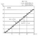
도 19에 도시한 결과를 그래프로 도시하면, 도 20과 같이 된다. 도 20은, 2bit TDC의 확장 코드를, 3bit TDC의 디코드 처리로 디코드한 결과의 이상적인 디코드값과 실제의 디코드값을 각각 플롯한 그래프이다. 도 20에서, 둥근점은, 이상적인 디코드값을 플롯한 그래프이다. 또한 사각점은, 실제의 디코드값을 플롯한 그래프이고, 클록 신호(CLKB)와 클록 신호(CLKD)를, 각각 Low인 상태에서 정지한 때에 얻어지는 디코드값을 플롯한 그래프이다.The graph shown in FIG. 19 shows the result as shown in FIG. 20 is a graph in which the ideal decoded value and the actual decoded value of the result of decoding the 2-bit TDC extension code by the 3-bit TDC decoding process are plotted, respectively. In Fig. 20, a smooth point is a graph plotting an ideal decode value. The blind spot is a graph plotting actual decode values, and is a graph plotting the decode values obtained when the clock signal CLKB and the clock signal CLKD are respectively stopped in a low state.
도 20은, 횡축에 시간, 종축에 디코드값을 취하고, A/D 변환의 리니어리티(입력된 신호에 대해, 출력되는 신호의 충실도)를 도시한 도면이다. 도 20으로부터, 이상적인 디코드값과 실제의 디코드값은 괴리되어 있다는 것을 알 수 있다. 참고를 위해, 도 21에, 3bit TDC의 확장 코드를, 3bit TDC의 디코드 처리로 디코드한 결과의 이상적인 디코드값과 실제의 디코드값을 각각 플롯한 그래프를 도시한다. 이 경우, 3bit TDC의 확장 코드를, 3bit TDC의 디코드 처리로 디코드하고 있기 때문에, 이상적인 디코드값과 실제의 디코드값은 일치한다. 이와 같이, 가능한 한, 이상적인 디코드값과 실제의 디코드값이 일치하는 것이 바람직하다.Fig. 20 is a diagram showing linearity of the A / D conversion (fidelity of the output signal with respect to the input signal) by taking the time on the horizontal axis and the decode value on the vertical axis. It can be seen from FIG. 20 that there is a difference between the ideal decode value and the actual decode value. For reference, Fig. 21 shows a graph in which the ideal decoded value and the actual decoded value of the result of decoding the extension code of the 3-bit TDC by the decode processing of the 3-bit TDC are shown, respectively. In this case, since the extension code of the 3-bit TDC is decoded by the decoding process of the 3-bit TDC, the ideal decode value and the actual decode value coincide. In this way, it is preferable that the ideal decode value and the actual decode value coincide as much as possible.
즉, 클록 신호를 정지시킨 때에, 이상적인 디코드값에 가능한 한 가까운 디코드값이 나오게되는 것이 바람직하다. 그러나, 후술하는 처리를 행하지 않는다면, 도 20에 도시한 바와 같이, 2개의 클록 신호를 정지시킨 때, 이상적인 디코드값과 실제의 디코드값은 괴리되어 버린다.In other words, when the clock signal is stopped, it is preferable that the decode value as close as possible to the ideal decode value is obtained. However, unless the processing described later is performed, as shown in Fig. 20, when the two clock signals are stopped, the ideal decode value and the actual decode value are separated.
마찬가지로, 1bit TDC의 확장 코드를, 3bit TDC의 디코드 처리로 디코드한 때에 관해 설명한다. 도 22는, 1bit TDC의 확장 코드를, 3bit TDC의 디코드 처리로 디코드한 결과를 도시한다. 1bit TDC일 때에는, 클록 신호(CLKB)는 정지되어 있기 때문에, 그 출력은, 0이다. 마찬가지로, 1bit TDC일 때에는, 클록 신호(CLKC)와 클록 신호(CLKD)는 이미 정지되어 있기 때문에, 그 출력은, 함께 0이다. 이 3개의 클록 신호에 의한 값은, 1bit TDC일 때에는 본래 사용되지 않지만, 잘못하여 3bit TDC로서 처리되면, 이 3개의 클록 신호에 의한 값도 처리되어 버린다.Similarly, a description will be given when the extended code of the 1-bit TDC is decoded by the decoding process of the 3-bit TDC. Fig. 22 shows the result of decoding an extension code of 1 bit TDC by decoding processing of 3 bit TDC. In the case of 1-bit TDC, since the clock signal CLKB is stopped, its output is zero. Similarly, in the case of 1-bit TDC, since the clock signal CLKC and the clock signal CLKD are already stopped, their outputs are 0 together. The values of these three clock signals are not originally used in the case of 1-bit TDC, but if they are mistakenly processed as 3-bit TDCs, the values of these three clock signals are also processed.
그 결과, 도 13을 참조하여 설명한 바와 같이, 1bit TDC일 때에는, 본래, 가산치로서는, 0, 0, 0, 0, 4, 4, 4, 4가 되지만, 도 22에 도시한 바와 같이 1bit TDC의 확장 코드를, 3bit TDC의 디코드 처리로 디코드하여 버리면, 그 디코드값은, 0, 0, 0, 0, 7, 7, 7, 7이 되어 버린다. 이 것을, 그래프로 도시하면, 도 23과 같이 된다. 도 23은, 1bit TDC의 확장 코드를, 3bit TDC의 디코드 처리로 디코드한 결과의 이상적인 디코드값과 실제의 디코드값을 각각 플롯한 그래프이다.As a result, as described with reference to FIG. 13, in the case of 1-bit TDC, the addition value is 0, 0, 0, 0, 4, 4, 4, 4, but as shown in FIG. 22, 1-bit TDC as shown in FIG. If the decoded extension code is decoded by the 3-bit TDC decoding process, the decode value is 0, 0, 0, 0, 7, 7, 7, 7. This is shown in a graph, as shown in FIG. Fig. 23 is a graph in which the ideal decoded value and the actual decoded value of the result of decoding the 1-bit TDC extension code by the 3-bit TDC decoding process are plotted, respectively.
도 23에서, 둥근점은, 이상적인 디코드값을 플롯한 그래프이다. 또한 사각점은, 실제의 디코드값을 플롯한 그래프이고, 클록 신호(CLKB), 클록 신호(CLKC), 및 클록 신호(CLKD)를, 각각 Low인 상태에서 정지한 때에 얻어지는 디코드값을 플롯한 그래프이다.In Fig. 23, a smooth point is a graph plotting an ideal decode value. In addition, a blind spot is a graph which plotted the actual decoded value, and is a graph which plotted the decoded value obtained when stopping the clock signal CLKB, the clock signal CLKC, and the clock signal CLKD in the low state, respectively. to be.
도 23은, 횡축에 시간, 종축에 디코드값을 취하고, A/D 변환의 리니어리티를 도시한 도면이다. 도 23으로부터, 이상적인 디코드값과 실제의 디코드값에서는, 괴리되어 있음을 읽을 수 있다. 이 경우도, 클록 신호를 정지시킨 때에, 이상적인 디코드값에 가능한 한 가까운 디코드값이 나오게 되는 것이 바람직하지만, 후술하는 처리를 행하지 않는다면, 도 23에 도시한 바와 같이, 3개의 클록 신호를 정지시킨 때, 이상적인 디코드값과 실제의 디코드값이 괴리되어 버린다.Fig. 23 is a diagram showing linearity of A / D conversion with time on the horizontal axis and decode on the vertical axis. It can be read from FIG. 23 that there is a difference between the ideal decode value and the actual decode value. Also in this case, when the clock signal is stopped, it is preferable that the decode value as close to the ideal decode value as possible comes out. However, when the clock signals are stopped as shown in FIG. The ideal decoded value and the actual decoded value are separated.
이와 같이, 클록 신호를 정지하면, 이상적인 디코드값과 실제의 디코드값이 괴리되고, 리니어리티가 악화되어 버리는 것이 생각된다. 리니어리티가 악화되지 않도록, 후술하는 처리가 행하여진다. 그 처리에 관해 설명하기 전에, 클록 신호를 정지시킴에 의해 단조증가성이 소실할 가능성이 있음에 관해 설명을 가한다.In this way, when the clock signal is stopped, it is conceivable that the ideal decoded value and the actual decoded value are different from each other and the linearity deteriorates. The processing described below is performed so that the linearity does not deteriorate. Before describing the processing, an explanation is given that there is a possibility that monotonic increase is lost by stopping the clock signal.
도 24는 클록 신호를 정지시킨 때, 즉 분해능이 다른 TDC의 이음매(joint)에 있어서의 디코드값을 나타내여 있다. 도 22에 도시한 예에서는, 이음매의 부분에서 가산치가 상승 및 하강하여 단조증가성이 소실하고 있음을 알 수 있다. 즉, 3bit TDC로부터 2bit TDC로 동작 모드가 전환되기 전의 디코드값은 3인데, 후의 디코드값은, 1, 다시 그 후의 시점에서의 디코드값은 6으로 되어 있다.Fig. 24 shows the decode value at the time of stopping the clock signal, that is, at the joint of TDCs having different resolutions. In the example shown in FIG. 22, it can be seen that the monotonic increase is lost due to the increase and decrease of the added value in the portion of the joint. In other words, the decode value before the operation mode is switched from the 3 bit TDC to the 2 bit TDC is 3, the decode value after the 1 is 1, and the decode value at the subsequent time is 6.
본래, 3bit TDC인 채라면, 도 5에 도시한 바와 같이, 그 디코드값은, 0, 1, 2, 3, 4, 5, 7, 8로 단조증가한다. 또한, 2bit TDC라면, 도 10에 도시한 바와 같이, 그 디코드값은, 0, 0, 2, 2, 4, 4, 6, 6으로 단조증가한다. 그러나, 3bit TDC로부터 2bit TDC로 동작 모드가 전환된 때의 타이밍에서 의해, 그 디코드값은, 예를 들면 도 24에 도시한 바와 같이, 0, 1, 2, 3, 1, 6, 6, 7, 7로 단조증가하지 않는 경우가 있다. 도시는 하지 않지만, 2bit TDC로부터 1bit TDC로 변환된 때에도, 단조증가는 하지 않는 경우가 있다.Originally, if it is 3bit TDC, as shown in Fig. 5, the decoding value monotonously increases to 0, 1, 2, 3, 4, 5, 7, 8. In addition, if it is a 2-bit TDC, as shown in FIG. 10, the decoding value monotonically increases to 0, 0, 2, 2, 4, 4, 6, 6. However, at the timing when the operation mode is switched from the 3 bit TDC to the 2 bit TDC, the decode value is 0, 1, 2, 3, 1, 6, 6, 7 as shown in FIG. 24, for example. For example, there is a case where the monotonism does not increase to 7, Although not shown, monotonic increase may not be performed even when it is converted from 2 bit TDC to 1 bit TDC.
이와 같이, 클록 신호를 정지한 때에, 단조증가성이 소실할 가능성이 있고, 단조증가성이 소실함으로써, 소실한 때의 디코드값의 정밀도가 저하되어 버릴 가능성이 있다. 그래서, 이하에 설명하는 바와 같은 처리가 행하여짐으로써, 단조증가성이 소실하여 버리는 것을 막도록 한다.As described above, when the clock signal is stopped, the monotonic increaseability may be lost, and the monotonic increaseability may be lost, and thus the accuracy of the decoded value at the time of the loss may be reduced. Therefore, the process as described below is performed to prevent the monotonic increase from being lost.
[제1-1의 실시의 형태에 관해][About Embodiment 1-1]
상기한 리니어리티의 악화와, 단조증가성의 소실을 고려한 처리에 관해 설명한다. 우선, 클록 신호를 정지시킬 때의 논리값을 궁리함에 의해, 리니어리티의 악화와, 단조증가성의 소실을 완화하는 처리에 관해 설명한다.The processing considering the deterioration of the linearity and the loss of monotone increase will be described. First, a process of mitigating the deterioration of linearity and the loss of monotone increase by devising a logic value at the time of stopping the clock signal will be described.
도 19, 도 22를 재차 참조한다. 도 19는, 2bit TDC의 확장 코드를, 3bit TDC의 디코드 처리로 디코드한 결과를 도시하는 도면이였다. 도 19에서, 클록 신호(CLKB)와 클록 신호(CLKD)는, 함께 정지되어 있는 상태이고, Low로 고정(이하, Lo 고정으로 기술)되어 있다. 그 때문에, 논리값은 0이 된다. 마찬가지로, 도 22에서, 클록 신호(CLKB), 클록 신호(CLKC), 및 클록 신호(CLKD)는, 함께 정지되어 있는 상태이고, Lo 고정되어 있다. 그 때문에, 논리값은 0이 된다.Reference is again made to FIGS. 19 and 22. 19 is a diagram showing a result of decoding an extension code of a 2-bit TDC by decoding processing of a 3-bit TDC. In Fig. 19, the clock signal CLKB and the clock signal CLKD are in a stopped state together, and are fixed to Low (hereinafter, referred to as Lo fixing). Therefore, the logical value is zero. Similarly, in FIG. 22, the clock signal CLKB, the clock signal CLKC, and the clock signal CLKD are stopped together and Lo is fixed. Therefore, the logical value is zero.
도 16을 재차 참조한다. 도 16은, A/D 변환 기간과 4개의 클록 신호의 동작 기간을 도시하는 도면이였다. 도 16에서, 클록 신호(CLKB)와 클록 신호(CLKD)는, 3bit TDC의 모드로부터 2bit TDC의 모드로 전환된 때에 정지되어, 각각 Lo 정지되어 있음을 알 수 있다. 또한, 2bit TDC의 모드로부터 1bit TDC의 모드로 전환되면, 클록 신호(CLKC)도 정지되는데, 클록 신호(CLKC)도, Lo 정지되어 있다.Reference is again made to FIG. 16. FIG. 16 is a diagram illustrating an A / D conversion period and an operation period of four clock signals. In Fig. 16, it can be seen that the clock signal CLKB and the clock signal CLKD are stopped when switching from the 3 bit TDC mode to the 2 bit TDC mode, and Lo stopped. In addition, when switching from the mode of 2 bit TDC to the mode of 1 bit TDC, the clock signal CLKC is also stopped, and the clock signal CLKC is also Lo stopped.
이와 같이, 모드의 전환시에, 정지시키는 클록 신호를 Low로 정지시키는 것이 아니라, High로 정지(이하, "Hi 정지"라고 한다)시키도록 한다. 환언하면, 모드의 전환시에, 정지시키는 클록 신호의 논리값이 0이 되는 상태에서 정지시키는 것이 아니고, 1이 되는 상태에서 정지시키도록 한다.In this manner, when the mode is switched, the clock signal to be stopped is not stopped at Low but is stopped at High (hereinafter referred to as "Hi Stop"). In other words, instead of stopping in the state where the logic value of the clock signal to be stopped becomes 0 at the time of mode switching, it is made to stop in the state which becomes 1.
구체적으로는, 도 25에 도시하는 바와 같이, 예를 들면 백 영역에서 클록 신호를 정지시키는 경우에 있어서, 클록 신호의 하나인 클록 신호(CLKB)를 정지시킬 때, Lo 고정이 아니라 Hi 고정으로 한다. 도 25에서, 실선은, 실제의 동작을 나타낸다. 클록 신호(CLKB)는, 3bit TDC로부터 2bit TDC의 모드로 전환될 때, Hi 정지되어, High인 상태가 유지된 상태에서 정지되어 있다. 클록 신호(CLKC)는, 2bit TDC로부터 1bit TDC의 모드로 전환될 때, Lo 정지되어, Low인 상태가 유지된 상태에서 정지되어 있다. 클록 신호(CLKD)는, 3bit TDC로부터 2bit TDC의 모드로 전환될 때, Lo 정지되어, Low인 상태가 유지된 상태에서 정지되어 있다.Specifically, as shown in FIG. 25, when the clock signal is stopped in the back region, for example, when the clock signal CLKB, which is one of the clock signals, is stopped, it is set to Hi fixed rather than Lo fixed. . In FIG. 25, the solid line shows the actual operation. When the clock signal CLKB is switched from the 3 bit TDC to the 2 bit TDC mode, the clock signal CLKB is stopped and is stopped while the high state is maintained. When the clock signal CLKC is switched from the 2-bit TDC to the 1-bit TDC mode, Lo stops and stops while the low state is maintained. When the clock signal CLKD is switched from the 3 bit TDC to the 2 bit TDC mode, the clock signal CLKD is Lo stopped and stopped while the low state is maintained.
이 경우, 모드가 전환될 때에 Hi 정지되는 것은, 하나의 클록 신호(클록 신호(CLKB))뿐인 예를 나타냈다. 여기서는, 하나의 클록 신호가 Hi 정지된 예를 들어서 설명하지만, 하나의 클록 신호만이 Hi 정지되는 것으로 한정하는 기재가 아니다.In this case, the example where only one clock signal (clock signal CLKB) stops Hi when the mode is switched is shown. Here, an example in which one clock signal is Hi stopped will be described. However, the description is not limited to that only one clock signal is Hi stopped.
예를 들면, 3bit TDC로부터 2bit TDC의 모드로 전환될 때, 클록 신호(CLKD)도 정지되기 때문에, 클록 신호(CLKD)도 클록 신호(CLKB)와 같이, Hi 정지되도록 하여도 좋다. 또한, 클록 신호(CLKB)는 Lo 정지되고, 클록 신호(CLKD)가 Hi 정지되도록 하여도 좋다. 또한, 2bit TDC로부터 1bit TDC의 모드로 전환될 때, 클록 신호(CLKC)도 Hi 정지되도록 하여도 좋다.For example, since the clock signal CLKD is also stopped when switching from the 3 bit TDC to the 2 bit TDC mode, the clock signal CLKD may be made to be stopped Hi like the clock signal CLKB. The clock signal CLKB may be Lo stopped, and the clock signal CLKD may be stopped Hi. In addition, when switching from the 2 bit TDC to the 1 bit TDC mode, the clock signal CLKC may also be stopped Hi.
또한, 어느 클록 신호를 Hi 정지시키고, 어느 클록 신호를 Lo 정지시키든지는, 설계 단계 등에서, 시뮬레이션함으로써 결정되도록 하는 것이 가능하다. 또한, 후술하는 도 28에, 시뮬레이션 결과를 도시하고, 설명을 한다.Further, it is possible to determine which clock signal is to be stopped Hi and which clock signal is to be stopped Lo by simulation at the design stage or the like. In addition, the simulation result is shown and demonstrated in FIG. 28 mentioned later.
여기서는, 클록 신호(CLKB)가, 3bit TDC로부터 2bit TDC의 모드로 전환될 때에, Hi 정지되고, 다른 클록 신호는, Lo 정지된다고 하여 설명을 계속한다. 이와 같이 클록 신호가 정지되는 경우, 클록 신호가 정지되어 있는 기간에서의 EB[2]은, 논리값 "0"이 아닌 논리값 "1"이 기억되게 된다. 이것을 디코드 처리의 알고리즘에 적용시키면, 리니어리티의 악화를 막고, 단조증가성이 소실하여 버리는 것을 완화하는 것이 가능해진다.Here, when the clock signal CLKB is switched from the 3 bit TDC to the 2 bit TDC mode, Hi is stopped and the other clock signals are Lo stopped. When the clock signal is stopped in this manner, the logic value "1" rather than the logic value "0" is stored in the EB [2] in the period in which the clock signal is stopped. Applying this to an algorithm for decoding processing makes it possible to prevent the deterioration of linearity and to reduce the loss of monotone increaseability.
그 것에 관해 도 26을 참조하여 설명한다. 도 26은, 2bit TDC 모드로 래치된 확장 코드를, 3bit TDC의 디코드 처리로 디코드한 결과를 도시하는 도면이다. 이 도 26은, 도 19에 대응하고 있다. 도 19는, 클록 신호(CLKB)를 Lo 정지한 때의 2bit TDC의 확장 코드를, 3bit TDC의 디코드 처리로 디코드한 결과를 도시하는 도면임에 대해, 도 26은, 클록 신호(CLKB)를 Hi 정지한 때의 2bit TDC의 확장 코드를, 3bit TDC의 디코드 처리로 디코드한 결과를 도시하는 도면인 점이 다르다.This will be described with reference to FIG. 26. Fig. 26 is a diagram showing a result of decoding the extension code latched in the 2bit TDC mode by decoding processing of 3bit TDC. This FIG. 26 corresponds to FIG. FIG. 19 shows the result of decoding the 2-bit TDC extension code when the clock signal CLKB is Lo-stopped by the 3-bit TDC decoding process, while FIG. 26 shows the clock signal CLKB as Hi. The diagram shows the result of decoding the 2-bit TDC extension code at the time of stop by decoding processing of the 3-bit TDC.
도 19를 재차 참조하면, 2bit TDC일 때에는, 본래, 가산치(디코드값)로서는, 0, 0, 2, 2, 4, 4, 6, 6이 되지만, 2bit TDC의 확장 코드를, 3bit TDC의 디코드 처리로 디코드하고, 클록 신호(CLKB)를 정지시킬 때, Lo 정지하여 버리면, 그 디코드값은, 0, 0, 1, 1, 6, 6, 7, 7이 되어 버린다. 이 경우, 이상치와 실제의 디코드값과의 차분을 취하면, 0, 0, -1, -1, 2, 2, 1, 1이 된다.Referring again to FIG. 19, in the case of a 2-bit TDC, the addition value (decode value) is originally 0, 0, 2, 2, 4, 4, 6, 6, but the extension code of the 2-bit TDC is converted into the 3-bit TDC. When decoding is performed by decoding processing and Lo stops when the clock signal CLKB is stopped, the decoded value is 0, 0, 1, 1, 6, 6, 7, 7. In this case, the difference between the outlier and the actual decode value is 0, 0, -1, -1, 2, 2, 1, 1.
그러나, 도 26에 도시하는 바와 같이, 2bit TDC의 확장 코드를, 3bit TDC의 디코드 처리로 디코드하여도, 클록 신호(CLKB)를 정지시킬 때, Hi 정지하면, 그 디코드값은, 1, 1, 2, 2, 5, 5, 6, 6이 된다. 이 경우, 이상치와 실제의 디코드값과의 차분을 취하면, 1, 1, 0, 0, 1, 1, 0, 0이 된다.However, as shown in Fig. 26, even when the extension code of the 2-bit TDC is decoded by the decoding process of the 3-bit TDC, when the clock signal CLKB is stopped, if Hi is stopped, the decode value is 1, 1, 2, 2, 5, 5, 6 and 6. In this case, the difference between the outlier and the actual decode value is 1, 1, 0, 0, 1, 1, 0, 0.
도 19에 도시한 바와 같이, 클록 신호(CLKB)를 정지시킬 때, Lo 정지하면, 이상치와 실제의 디코드값과의 차분은, 최대로 2가 됨에 대해, 도 26에 도시한 바와 같이, 클록 신호(CLKB)를 정지시킬 때, Hi 정지하면, 이상치와 실제의 디코드값과의 차분은, 최대로 1이 된다. 즉, 클록 신호(CLKB)를 정지시킬 때, Hi 정지함으로써, 이상치와의 괴리가 작아짐을 알 수 있다.As shown in FIG. 19, when Lo stops when the clock signal CLKB is stopped, the difference between the outlier and the actual decode value becomes 2 at maximum. As shown in FIG. 26, the clock signal When Hi stops when (CLKB) is stopped, the difference between the outlier and the actual decode value is at most 1. In other words, when the clock signal CLKB is stopped, Hi stops the deviation from the outlier.
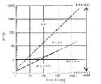
또한, 이에 관해, 도 27을 참조한다. 도 27은 횡축에 시간, 종축에 디코드값을 취하고, A/D 변환의 리니어리티를 도시한 것이다. 이 도 27은, 도 20에 대응하고 있다. 도 20은, Lo 정지한 때의 A/D 변환의 리니어리티를 도시한 것이고, 도 27은, Hi 정지한 때의 A/D 변환의 리니어리티를 도시한 것이다. 도 20과 도 27을 비교하면, 분명히, 도 27에 도시한 경우의 쪽이, 도 20에 도시한 경우에 대해, 이상치와 실제의 디코드값이 괴리되지 않고, 이상적인 디코드값에 가까운 값으로, 실제의 디코드값이 플롯되어 있는 것을 읽을 수 있다.See also FIG. 27 in this regard. Fig. 27 shows linearity of A / D conversion by taking time on the horizontal axis and decoded values on the vertical axis. This FIG. 27 corresponds to FIG. 20 shows the linearity of the A / D conversion when Lo stops, and FIG. 27 illustrates the linearity of the A / D conversion when Hi stops. Comparing FIG. 20 with FIG. 27, apparently, in the case of FIG. 27, the outliers and the actual decoded values do not differ from each other in the case shown in FIG. You can read that the decoded values of are plotted.
이와 같이, 클록 신호를 정지시킬 때, High인 상태에서 정지시킴으로써, 리니어리티가 개선한다.In this way, when stopping the clock signal, the linearity is improved by stopping in the high state.
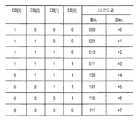
상기한 바와 같이, Hi 정지시키는 클록 신호는 클록 신호(CLKB)로 한하지 않고, 다른 클록 신호(클록 신호(CLKD))를 Hi 정지시켜서도 좋다. 도 28에, 클록 신호(CLKB) 또는/및 클록 신호(CLKC)를 Lo 정지 또는/및 Hi 정지시킨 때의 조합에 의한 최대 오차를 도시한다.As described above, the clock signal to stop Hi is not limited to the clock signal CLKB, but may stop the other clock signal (clock signal CLKD). FIG. 28 shows the maximum error due to the combination of when the clock signal CLKB and / or the clock signal CLKC is Lo-stopped and / or Hi-stopped.
클록 신호(CLKB)와 클록 신호(CLKD) 양쪽 모두를 Lo 정지로 한 경우, 최대 오차는, 2LSB가 된다. 클록 신호(CLKB)와 클록 신호(CLKD)를 함께 Hi 정지한 경우, 최대 오차는, 2LSB가 된다. 클록 신호(CLKB)를 Lo 정지하고, 클록 신호(CLKD)를 Hi 정지한 경우, 최대 오차는, 1LSB가 된다. 클록 신호(CLKB)를 Hi 정지하고, 클록 신호(CLKD)를 Lo 정지한 경우, 최대 오차는, 1LSB가 된다.When both the clock signal CLKB and the clock signal CLKD are set to Lo stop, the maximum error is 2LSB. When the clock signal CLKB and the clock signal CLKD are stopped at the same time, the maximum error is 2LSB. When Lo stops the clock signal CLKB and Hi stops the clock signal CLKD, the maximum error is 1LSB. When Hi stops the clock signal CLKB and Lo stops the clock signal CLKD, the maximum error is 1LSB.
이 결과, 클록 신호(CLKB) 또는 클록 신호(CLKD)의 어느 한쪽을, Hi 정지함으로써, 최대 오차를 1LSB로 억제할 수 있음을 알 수 있다. 따라서, 3bit TDC로부터 2bit TDC의 모드로 전환할 때, 클록 신호(CLKB) 또는 클록 신호(CLKD)의 어느 한쪽을, Hi 정지함으로써, 리니어리티가 개선한다.As a result, it is understood that the maximum error can be suppressed to 1LSB by Hi stopping either the clock signal CLKB or the clock signal CLKD. Therefore, when switching from the 3-bit TDC to the 2-bit TDC mode, the linearity is improved by Hi-stopping either the clock signal CLKB or the clock signal CLKD.
다음에, 1bit TDC의 경우에 관해 설명한다. 도 29는, 1bit TDC 모드로 래치된 확장 코드를, 3bit TDC의 디코드 처리로 디코드한 결과를 도시하는 도면이다. 이 도 29는, 도 22에 대응하고 있다. 도 22는, 클록 신호(CLKC)를 Lo 정지한 때의 1bit TDC의 확장 코드를, 3bit TDC의 디코드 처리로 디코드한 결과를 도시하는 도면임에 대해, 도 29는, 클록 신호(CLKC)를 Hi 정지한 때의 1bit TDC의 확장 코드를, 3bit TDC의 디코드 처리로 디코드한 결과를 도시하는 도면인 점이 다르다.Next, the case of 1-bit TDC will be described. Fig. 29 is a diagram showing the result of decoding the extension code latched in the 1-bit TDC mode by decoding processing of a 3-bit TDC. 29 corresponds to FIG. 22. FIG. 22 is a diagram showing the result of decoding the 1-bit TDC extension code when the clock signal CLKC is Lo-stopped by the 3-bit TDC decoding process. FIG. 29 shows the clock signal CLKC as Hi. The diagram shows the result of decoding the 1-bit TDC extension code at the time of stop by decoding processing of the 3-bit TDC.
도 22를 재차 참조하면, 1bit TDC일 때에는, 본래, 가산치(디코드값)로서는, 0, 0, 0, 0, 4, 4, 4, 4가 되지만, 1bit TDC의 확장 코드를, 3bit TDC의 디코드 처리로 디코드하고, 클록 신호(CLKC)를 정지시킬 때, Lo 정지하여 버리면, 그 디코드값은, 0, 0, 0, 0, 7, 7, 7, 7이 되어 버린다. 이 경우, 이상치와 실제의 디코드값과의 차분을 취하면, 0, 0, 0, 0, 3, 3, 3, 3이 된다.Referring again to Fig. 22, in the case of 1-bit TDC, the addition value (decode value) is originally 0, 0, 0, 0, 4, 4, 4, 4, but the extension code of 1-bit TDC is converted to 3-bit TDC. When decoding is performed by decoding processing and Lo stops when the clock signal CLKC is stopped, the decoded value is 0, 0, 0, 0, 7, 7, 7, 7. In this case, the difference between the outlier and the actual decode value is 0, 0, 0, 0, 3, 3, 3, 3.
그러나, 도 29에 도시하는 바와 같이, 1bit TDC의 확장 코드를, 3bit TDC의 디코드 처리로 디코드하여도, 클록 신호(CLKC)를 정지시킬 때, Hi 정지하면, 그 디코드값은, 1, 1, 1, 1, 6, 6, 6, 6이 된다. 이 경우, 이상치와 실제의 디코드값과의 차분을 취하면, 1, 1, 1, 1, 2, 2, 2, 2가 된다.However, as shown in Fig. 29, even when the 1-bit TDC extension code is decoded by the 3-bit TDC decode process, when the clock signal CLKC is stopped, if Hi is stopped, the decode value is 1, 1, 1, 1, 6, 6, 6, 6. In this case, the difference between the outlier and the actual decode value is 1, 1, 1, 1, 2, 2, 2, 2.
도 22에 도시한 바와 같이, 클록 신호(CLKC)를 정지시킬 때, Lo 정지하면, 이상치와 실제의 디코드값과의 차분은, 최대로 3이 됨에 대해, 도 29에 도시한 바와 같이, 클록 신호(CLKC)를 정지시킬 때, Hi 정지하면, 이상치와 실제의 디코드값과의 차분은, 최대로 2가 된다. 즉, 클록 신호(CLKC)를 정지시킬 때, Hi 정지함으로써, 이상치와의 괴리가 작아짐을 알 수 있다.As shown in FIG. 22, when Lo stops when the clock signal CLKC is stopped, the difference between the outlier and the actual decode value is 3 at maximum. As shown in FIG. 29, the clock signal When stopping (CLKC) stops Hi, the difference between the outlier and the actual decode value is at most 2. In other words, when the clock signal CLKC is stopped, it is understood that Hi stops the deviation from the outlier.
또한, 이에 관해, 도 30을 참조한다. 도 30은 횡축에 시간, 종축에 디코드값을 취하고, A/D 변환의 리니어리티를 도시한 것이다. 이 도 30은, 도 23에 대응하고 있다. 도 23은, Lo 정지한 때의 A/D 변환의 리니어리티를 도시한 것이고, 도 30은, Hi 정지한 때의 A/D 변환의 리니어리티를 도시한 것이다. 도 23과 도 30을 비교하면, 분명히, 도 30에 도시한 경우의 쪽이, 도 23에 도시한 경우에 대해, 이상치와 실제의 디코드값이 괴리되지 않고, 이상적인 디코드값에 가까운 값으로, 실제의 디코드값이 플롯되어 있는 것을 읽을 수 있다.See also FIG. 30 in this regard. Fig. 30 shows linearity of A / D conversion by taking time on the horizontal axis and decoded values on the vertical axis. This FIG. 30 corresponds to FIG. FIG. 23 shows the linearity of A / D conversion when Lo stops, and FIG. 30 shows the linearity of A / D conversion when Hi stops. When FIG. 23 is compared with FIG. 30, it is clear that the case shown in FIG. 30 is not different from the ideal value and the actual decode value in the case shown in FIG. You can read that the decoded values of are plotted.
이와 같이, 클록 신호를 정지시킬 때, High인 상태에서 정지시킴으로써, 리니어리티가 개선한다.In this way, when stopping the clock signal, the linearity is improved by stopping in the high state.
클록 신호(CLKC)가 정지될 때에는, 이미 클록 신호(CLKB)와 클록 신호(CLKD)는 정지되어 있는 상태이다. 이들의 3개의 클록 신호를, 각각 정지할 때에, Hi 정지하는지 또는 Lo 정지하는지에 의해, 최대 오차가 달라진다. 그래서, 도 31에, 1bit TDC에서 정지시키는 3개의 클록 신호(CLKB, CLKC, CLKD)를 정지시키는 논리의 조합과, 그 때의 최대 오차를 도시한다.When the clock signal CLKC is stopped, the clock signal CLKB and the clock signal CLKD are already stopped. The maximum error varies depending on whether Hi or Lo stops these three clock signals, respectively. Therefore, Fig. 31 shows a combination of logic for stopping three clock signals CLKB, CLKC, and CLKD to stop at 1-bit TDC, and the maximum error at that time.
클록 신호(CLKB), 클록 신호(CLKC), 및 클록 신호(CLKD)를 함께 Lo 정지로 한 경우, 최대 오차는, 3LSB가 된다. 클록 신호(CLKB)와 클록 신호(CLKD)를 함께 Lo 정지하고, 클록 신호(CLKC)를 Hi 정지한 경우, 최대 오차는, 1LSB가 된다. 클록 신호(CLKB)와 클록 신호(CLKD)를 함께 Hi 정지하고, 클록 신호(CLKC)를 Lo 정지한 경우, 최대 오차는, 1LSB가 된다.When the clock signal CLKB, the clock signal CLKC, and the clock signal CLKD are set to Lo stop together, the maximum error is 3LSB. When the clock signal CLKB and the clock signal CLKD are Lo-stopped together and the clock signal CLKC is Hi-stopped, the maximum error is 1LSB. When the clock signal CLKB and the clock signal CLKD are stopped Hi together and the clock signal CLKC is Lo stopped, the maximum error is 1LSB.
클록 신호(CLKB), 클록 신호(CLKC), 및 클록 신호(CLKD)를 함께 Hi 정지로 한 경우, 최대 오차는, 3LSB가 된다. 클록 신호(CLKB)와 클록 신호(CLKC)를 함께 Lo 정지하고, 클록 신호(CLKD)를 Hi 정지한 경우, 최대 오차는, 1LSB가 된다. 클록 신호(CLKB)를 Lo 정지하고, 클록 신호(CLKC)와 클록 신호(CLKD)를 함께 Hi 정지한 경우, 최대 오차는, 1LSB가 된다.When the clock signal CLKB, the clock signal CLKC, and the clock signal CLKD are set to Hi stop together, the maximum error is 3LSB. When Lo stops the clock signal CLKB and the clock signal CLKC together and Hi stops the clock signal CLKD, the maximum error is 1LSB. When the clock signal CLKB is Lo-stopped and the clock signal CLKC and the clock signal CLKD are stopped Hi together, the maximum error is 1LSB.
클록 신호(CLKB)를 Hi 정지하고, 클록 신호(CLKC)와 클록 신호(CLKD)를 함께 Lo 정지한 경우, 최대 오차는, 1LSB가 된다. 클록 신호(CLKB)와 클록 신호(CLKC)를 함께 Hi 정지하고, 클록 신호(CLKD)를 Lo 정지한 경우, 최대 오차는, 1LSB가 된다.In the case where Hi stops the clock signal CLKB and Lo stops the clock signal CLKC and the clock signal CLKD together, the maximum error is 1LSB. In the case where the clock signal CLKB and the clock signal CLKC are stopped Hi together and the clock signal CLKD is Lo stopped, the maximum error is 1LSB.
이와 같기 때문에, 클록 신호(CLKB), 클록 신호(CLKC), 또는 클록 신호(CLKD)를 정지할 때, 하나 또는 2개의 클록 신호를 Hi 정지함으로써, 리니어리티가 개선딤을 알 수 있다.Thus, when the clock signal CLKB, the clock signal CLKC, or the clock signal CLKD is stopped, the linearity is improved by Hi stopping one or two clock signals.
또한, 3bit TDC로부터 2bit TDC로 동작 모드가 이행할 때, 도 28을 참조하여 설명한 바와 같이, 클록 신호(CLKB) 또는 클록 신호(CLKD)의 어느 한쪽을, Hi 정지함으로써, 리니어리티가 개선된다. 이것을 합쳐서 고려하면, 클록 신호(CLKB), 클록 신호(CLKC), 또는 클록 신호(CLKD)를 정지할 때, 클록 신호(CLKB) 또는 클록 신호(CLKD)의 어느 한쪽을, Hi 정지하고, 클록 신호(CLKC)는, Hi 정지, Lo 정지의 어느 쪽도 양호하다는 것을 알 수 있다.In addition, when the operation mode shifts from the 3 bit TDC to the 2 bit TDC, as described with reference to FIG. 28, the linearity is improved by Hi stopping either the clock signal CLKB or the clock signal CLKD. In consideration of this, when the clock signal CLKB, the clock signal CLKC, or the clock signal CLKD is stopped, either the clock signal CLKB or the clock signal CLKD is stopped and the clock signal is stopped. It turns out that (CLKC) is good for both Hi stop and Lo stop.
이와 같이, 소정의 영역(예를 들면, 백 영역)에서, 클록 신호를 정지시킬 때, High인 상태에서 정지시킴으로써, 리니어리티의 저하를 최소한으로 억제한 상태에서, 클록 신호를 정지시킴에 의한 소비 전력의 저감을 실현하는 것이 가능해진다.In this way, when the clock signal is stopped in a predetermined region (for example, the back region), by stopping in a high state, power consumption by stopping the clock signal in a state where the decrease in linearity is minimized. Can be realized.
또한, 이와 같이, Hi 정지함으로써, 단조증가성의 소실도 최소한으로 억제하는 것이 가능해진다. 이에 관해, 도 32를 참조하여 설명한다. 도 32는, 클록 신호를 정지시킨 때, 즉 분해능이 다른 TDC의 이음매에서의 디코드값을 도시하고 있다. 이 도 32는, 도 24에 대응하고 있다. 도 24는, 분해능이 다른 TDC의 이음매에서, 클록 신호를 Lo 정지한 때의 디코드값을 도시하는 도면임에 대해, 도 32는, 분해능이 다른 TDC의 이음매에서, 클록 신호를 Hi 정지한 때의 디코드값을 도시하는 도면인 점이 다르다.In addition, by stopping Hi in this way, it is possible to minimize the loss of monotone increase. This will be described with reference to FIG. 32. Fig. 32 shows the decode value at the time of stopping the clock signal, that is, at the joints of the TDCs having different resolutions. This FIG. 32 corresponds to FIG. FIG. 24 is a diagram showing a decoded value when the clock signal is Lo stopped at a seam of TDCs having different resolutions, while FIG. 32 is a diagram showing a hi-stop clock signal at a seam of TDCs having different resolutions. This is a diagram showing the decode value.
도 32에 도시한 예는, 3bit TDC로부터 2bit TDC의 모드로 전환될 때 클록 신호 CCKB가 Hi 정지될 때의 예이다. 이와 같은 경우의 디코드값은, 0, 1, 2, 3, 4, 5, 6, 7, 6이 된다. 3bit TDC로부터 2bit TDC의 모드로 전환될 때, 전환되기 전의 값은 "7"인 것에 대해, 전환된 후의 값은 "6"이 되어 있다. 이와 같이, "6", "7"로 와서 단조증가하는 것이면 다음은 "8"이 되지만, "6"이 되기 때문에, 단조증가성은 잃어버리게 되지만, 그 변화는 1로 작은 값이 된다.The example shown in FIG. 32 is an example when the clock signal CCKB is stopped Hi when switching from a 3 bit TDC to a 2 bit TDC mode. The decode value in such a case is 0, 1, 2, 3, 4, 5, 6, 7, 6. When switching from 3bit TDC to 2bit TDC mode, the value before switching is " 7 ", while the value after switching is " 6 ". In this way, if the monotonic increase comes to " 6 " and " 7 ", then the next becomes " 8 ", but since it becomes " 6, "
즉, 도 24에 도시한 예에서는, "1", "2", "3"의 이후에, 동작 모드가 전환되면, "1"이 되기 때문에, "3"부터 "1"로, "2"의 변화가 있다. 또한, 디코드값은, "1"의 뒤에, "6"이 되기 때문에 "5"의 변화가 있다. 이것과 비교하면, 단지 "1"의 변화라는 것은, 분명히 그 변화는 적고, 단조증가성이 소실하여 버렸다고 하여도, 최소한으로 억제되어 있음을 알 수 있다.That is, in the example shown in Fig. 24, when the operation mode is switched after "1", "2", and "3", it becomes "1", so that "2" from "3" to "1". There is a change. In addition, since the decoding value becomes "6" after "1", there is a change of "5". In comparison with this, it can be seen that the change of only "1" is clearly suppressed to a minimum even if the change is small and the monotonic increase is lost.
즉, 클록 신호를 정지할 때, Hi 정지함으로써, 단조증가성의 소실을 최소한으로 억제하는 것이 가능해진다. 환언하면, 클록 신호를 정지할 때, Hi 정지함으로써, 분해능이 다른 TDC의 이음매에서의 디코드값이 상승 및 하강하여 단조증가성이 소실하여 버려도, 그 단차는 작아지고, 악영향을 최소한으로 억제하는 것이 가능해진다.In other words, by stopping Hi when the clock signal is stopped, it becomes possible to minimize the loss of monotonic increase. In other words, when the clock signal is stopped, Hi stops, even if the decoding value at the joint of the TDC having different resolutions rises and falls, and the monotonic increase is lost, the step becomes small, and the adverse effect is minimized. It becomes possible.
이와 같이, 소정의 영역(예를 들면, 백 영역)에서, 클록 신호를 정지함으로써, 클록 신호를 정지한 분만큼, 적어도 소비 전력을 저감시키는 것이 가능해진다. 클록 신호를 정지시키는 것은, 분해능의 떨어짐으로 되지만, 분해능을 떨어뜨림에 의한 영향이 적은 영역(예를 들면, 백 영역)에서 분해능을 떨어뜨리기 때문에, 최종적인 디코드값에는 영향이 없이, 화질이 유지될 수 있다.In this manner, by stopping the clock signal in a predetermined region (for example, the back region), it is possible to reduce power consumption at least by the amount of the clock signal that has been stopped. Stopping the clock signal results in lower resolution, but lowers the resolution in a region (e.g., a back region) where the resolution is less affected. Therefore, image quality is maintained without affecting the final decode value. Can be.
따라서, 본 실시의 형태에 의하면, 소정의 영역에서 분해능을 떨어뜨림으로써(분해능을 전환함으로써), 화질을 떨어뜨리는 일 없이, 소비 전력을 떨어뜨리는 것이 가능해진다. 또한, 분해능을 떨어뜨릴 때에, 즉 클록 신호를 정지시킬 때에, 그 정지되는 클록 신호를 상태(Low 또는 High인 상태)를 적절하게 설정함으로써, 리니어리티가 저하되거나, 단조증가성이 소실하여 버리거나 하는 것을 최소한으로 억제하는 것이 가능해진다.Therefore, according to the present embodiment, the power consumption can be lowered without lowering the image quality by lowering the resolution (by switching the resolution) in the predetermined region. In addition, when the resolution is decreased, that is, when the clock signal is stopped, the state of the stopped clock signal is set appropriately (a state of low or high), whereby linearity is lowered or monotonic increaseability is lost. It can be suppressed to the minimum.
[제1-2의 실시의 형태에 관해][About Embodiment of 1-2]
상기한 제1-1의 실시의 형태에서는, 클록 신호를 정지시킬 때, 그 정지시키는 클록 신호를 High인 상태에서 정지시키는 예를 설명하였다. 이 제1-1의 실시의 형태에 의하면, 리니어리티가 저하되거나, 단조증가성이 소실하여 버리거나 하는 것을 최소한으로 억제할 수 있지만, 완전하게 억제하는 것은 곤란하다. 다음에, 리니어리티의 저하나 단조증가성의 소실을 완전히 억제하도록 하는 실시의 형태에 관해 설명한다.In the above-described embodiment 1-1, when the clock signal is stopped, an example of stopping the clock signal to be stopped in the high state has been described. According to the first-first embodiment, it is possible to minimize the decrease in linearity or the loss of monotone increaseability, but it is difficult to completely suppress it. Next, an embodiment in which the reduction of linearity and the loss of monotone increase is completely suppressed will be described.
이 실시의 형태에서는, 카운터의 상위 비트의 변화가 관측되고, 그 칼럼의 조도 및 분해능이 인식되고, 칼럼 전체에 분배된 복수의 디코드 제어로부터 각 칼럼의 분해능에 응하여 디코드 제어가 선택적으로 행하여진다. 이 실시의 형태에서도, 소정의 영역에서, 클록 신호가 정지되고, 그 정지될 때에 이하의 처리가 실행된다. 또한 이하에 설명하는 처리는, 도 18에 도시한 열병렬 ADC 탑재 고체 촬상 소자(CMOS 이미지 센서)에 적용되고, 복수의 A/D 변환 장치가 사용되고, 제어 신호가 공통으로 되어 있을 때에 행하여지는 처리이다.In this embodiment, the change of the upper bit of the counter is observed, the illuminance and the resolution of the column are recognized, and the decode control is selectively performed in response to the resolution of each column from the plurality of decode controls distributed throughout the column. Also in this embodiment, the clock signal is stopped in the predetermined area, and the following processing is executed when the clock signal is stopped. In addition, the process described below is applied to the solid-state image sensor (CMOS image sensor) with a column-parallel ADC shown in FIG. 18, and is a process performed when a plurality of A / D converters are used and control signals are common. to be.
도 33을 참조하여, 조도가 다름으로써 분해능이 각 칼럼에 의해 다른 TDC군에 대해, 각 칼럼에서 조도 및 분해능을 인식한 원리를 나타낸다. 도 3에 도시한 A/D 변환 회로(20)는, 적분형 A/D 변환 회로에 속하고, A/D 변환 기간을 업 카운트하여 가기 위해, 클록 신호를 정지하는 기간을, 카운터 값이 변화하는 포인트에 설정하여 두면, 역으로 카운터 값을 참조하는 구성으로 할 수 있다. 특히 상위 비트가 참조되도록 구성함으로써, 각 칼럼에서, 어느 A/D 변환 기간에서 VCO가 변화하고 확장 코드가 래치되었는지를 식별할 수 있다.Referring to Fig. 33, the principle of recognizing the illuminance and the resolution in each column for the TDC group in which the resolution differs by each column due to the different illuminance is shown. The A /
도 33에 도시한 예에서는, Q[12]와 Q[13]가 참조되고, Q[12]가 처음으로 "1"이 되었을 때 이후를, 2bit TDC로서 소정의 클록 신호를 정지시키고, 또한 그 후, Q[13]가 처음으로 "1"이 되었을 때 이후를, 1bit TDC로서 소정의 클록 신호를 정지시킨다. 또한, 논리 회로에서 Q[12]가 처음으로 "1"이 되었을 때 제어 신호(TDC2SEL)를 어서트(assert)하고, Q[13]가 처음으로 "1"이 되었을 때 제어 신호(TDC1SEL)를 어서트하도록에 처리한다. 이와 같이 처리되도록 함으로써, 각 칼럼에서 제어 신호(TDC2SEL)와 제어 신호(TDC1SEL)의 값으로 어느 영역에서 VCO가 변화하였는지를 알고, 이것을 이용하여 도 34에 대응하는 분해능의 디코드 처리가 행하여지도록 한다.In the example shown in Fig. 33, Q [12] and Q [13] are referenced, and when Q [12] first becomes " 1 ", the predetermined clock signal is stopped as a 2-bit TDC, and the After that, when Q [13] first becomes " 1 ", the predetermined clock signal is stopped as a 1-bit TDC. Further, in the logic circuit, the control signal TDC2SEL is asserted when Q [12] becomes "1" for the first time, and the control signal TDC1SEL is supplied when Q [13] becomes "1" for the first time. Handle to assert. By processing in this way, it is known in which region the VCO has changed by the values of the control signal TDC2SEL and the control signal TDC1SEL in each column, and the decoding process of the resolution corresponding to FIG. 34 is performed using this.
도 34를 참조하면, 제어 신호(TDC2SEL)와 제어 신호(TDC1SEL)가 함께 어서트(asserting)되지 않은 상태("0"인 상태)인 경우, 래치 디코드 회로(23)(도 3)는, 3bit TDC로서 기능한다. 제어 신호(TDC2SEL)가 어서트된 상태("1"인 상태)이고, 제어 신호(TDC1SEL)가 어서트되지 않은 상태("0"인 상태)인 경우, 래치 디코드 회로(23)는, 2bit TDC로서 기능한다. 제어 신호(TDC2SEL)와 제어 신호(TDC1SEL)가 함께 어서트되어 있는 상태("1"인 상태)인 경우, 래치 디코드 회로(23)는, 1bit TDC로서 기능한다. 제어 신호(TDC2SEL)가 어서트되지 않은 상태("0"인 상태)이고, 제어 신호(TDC1SEL)가 어서트되어 있는 상태("1"인 상태)는, 발생하지 않는 상태이기 때문에, 동작 모드로서는 규정되지 않는다. 가령, 이와 같은 상태가 발생한 경우에는, 에러 처리가 실행된다.Referring to FIG. 34, when the control signal TDC2SEL and the control signal TDC1SEL are not asserted together (“0”), the latch decode circuit 23 (FIG. 3) is 3 bits. It functions as a TDC. When the control signal TDC2SEL is in an asserted state ("1" state) and the control signal TDC1SEL is in an unasserted state ("0" state), the
이와 같은 처리를 행하는 A/D 변환 회로(20)는, 도 35에 도시하는 바와 같은 구성이 된다. 도 4에 도시한 A/D 변환 회로(20)와 동일한 부분은 동일한 부호를 붙이고, 그 설명은 생략한다. 도 35에 도시한 A/D 변환 회로(200)는, 도 4에 도시한 A/D 변환 회로(20)와 비교하여, TDC 분해능 변경 회로(201)가 추가된 구성으로 되어 있다.The A /
또한, 도 35에서는, 리플 카운터(24)를 구성하는 상위 비트의 리플 카운터인, 상위 비트 리플 카운터(202)를 도시하고 있다. 리플 카운터(24)는, 카운트하는 비트 수만큼 플립플롭을 구비하고 있는데, 그 중의, 상위 비트의 카운터인 플립플롭(221)과 플립플롭(222)을 도시하고 있다. 플립플롭(221)은, 상위 비트의 Q[x]를 카운트하고, 플립플롭(222)는, 상위 비트의 Q[y]를 카운트한다.In addition, in FIG. 35, the high order bit ripple counter 202 which is the high order ripple counter which comprises the
상기 x나 y는, 도 33을 참조하여 설명한 처리를 행하는 A/D 변환 회로(200)의 경우, "12"나 "13"이다. 그러나, x나 y는, "12"나 "13"으로 한정되는 것이 아니고, 리플 카운터(24) 내의 소정의 플립플롭에 접속되고, 그 출력을 참조할 수 있는 구성으로 되어 있으면 좋다. 또한, 연속하고 있는 플립플롭의 출력이 참조되는 실시의 형태로 한정되는 것이 아니고, 연속하지 않는 플립플롭의 출력이 참조되는 형태라도 좋다. 또한, 2개의 출력이 참조될 뿐만 아니라, 또다른 출력이 참조되도록 구성하는 것도 가능하다.The x and y are " 12 " or " 13 " in the case of the A /
TDC 분해능 변경 회로(201)는, 2개의 AND 회로와 1개의 OR 회로로 구성되는 AND-OR 회로(211), AND 회로(212), Muller의 C소자(213, 214)를 구비한다. Muller의 C소자는, 대기 소자(waiting element)로 알려지고 있고, 2입력의 양쪽이 갖추어진다면 출력을 그 값으로 하고 2입력이 다른 때에는 전의 출력치를 유지하고 출력하는 회로이다. AND-OR 회로(211)의 제1의 2입력 AND 회로의 제1의 입력단자는, 펄스 신호(EBCK2)의 공급 라인에 접속되어 있다. 제1의 2입력 AND 회로의 제2의 부입력단자에는, AND 회로(214)로부터의 제어 신호(TDC2SEL)가 공급된다.The TDC
AND-OR 회로(211)의 제2의 2입력 AND 회로의 제1의 입력단자는, 펄스 신호(EBCK1)의 공급 라인에 접속되어 있다. 제2의 2입력 AND 회로의 제2의 입력단자에는, Muller의 C소자(214)로부터의 제어 신호(TDC2SEL)가 공급된다. 제1의 2입력 AND 회로와 제2의 2입력 AND 회로로부터의 출력은, OR 회로에 공급된다. OR 회로로부터의 출력은, AND 회로(212)의 제1의 입력단자에 공급된다. AND 회로(212)의 제2의 부입력단자에는, Muller의 C소자(213)로부터의 제어 신호(TDC1SEL)가 공급된다.The first input terminal of the second two-input AND circuit of the AND-
AND 회로(212)로부터의 출력은, AND-OR 회로(61)의 제1의 3입력 AND 회로의 제1의 입력단자와, 제2의 3입력 AND 회로의 제1의 입력단자에, 펄스 신호(EBCK)로서 공급된다.The output from the AND
이와 같은 구성을 갖는 A/D 변환 회로(200)의 동작에 관해, 도 36A 내지 도 36C를 참조하여 설명한다. 도 36A 내지 도 36C는, 제어 신호의 파형을 도시한다. 도 36A는, 래치 디코드 회로(23)(도 3)가, 3bit TDC로서 기능하고 있을 때의 파형이고, 도 36B는, 2bit TDC로서 기능하고 있을 때의 파형이고, 도 36C는, 1bit TDC로서 기능하고 있을 때의 파형이다. 도 36에 도시한 제어 파형은, 래치 디코드 회로(23)에 공급되는 제어 신호의 파형이지만, 이 래치 디코드 회로(23)의 내용은, 도 35에 도시한 A/D 변환 회로(200)의 일부이다.The operation of the A /
도 36A 내지 도 36C에 도시한 제어 파형은, A/D 변환 회로(200)에 공급되는 제어 신호의 파형인데, 비교를 위해, 도 17A 내지 도 17C에 도시한 A/D 변환 회로(20)(도 4)에 공급되는 제어 신호의 파형을 재차 참조한다. 예를 들면, 도 17A와 도 36A를 비교한다. 도 17A에 대해, 도 36A에는, 제어 신호(EBCK2)와 제어 신호(EBCK1)가 추가되어 있음을 알 수 있다. 제어 신호(EBCK), 제어 신호(EBCKO), 제어 신호(XEBMSK), 및 제어 신호(EB4CK)는, A/D 변환 회로(20)와 A/D 변환 회로(200)에서 같은 제어를 행하기 위한 신호이다.The control waveforms shown in FIGS. 36A to 36C are waveforms of the control signals supplied to the A /
그러나, A/D 변환 회로(20)(도 4)에서, 제어 신호(EBCK)는, 외부로부터 공급되고, 각 칼럼에 공통되고 공급되는 신호임에 대해, A/D 변환 회로(200)(도 35)에서, 제어 신호(EBCK)는, 제어 신호(EBCK2)와 제어 신호(EBCK1)로부터 생성되는 신호인 점이 다르다. 환언하면, A/D 변환 회로(20)(도 4)에서, 제어 신호(EBCK)는, 외부로부터 공급되는 신호임에 대해, A/D 변환 회로(200)(도 35)에서, 제어 신호(EBCK)는, 자기 생성(self-generated) 신호이다.However, in the A / D conversion circuit 20 (FIG. 4), the control signal EBCK is a signal supplied from the outside and common to each column, and supplied to the A / D conversion circuit 200 (FIG. 4). In 35, the control signal EBCK is different from the control signal EBCK2 and the signal generated from the control signal EBCK1. In other words, in the A / D conversion circuit 20 (FIG. 4), the control signal EBCK is a signal supplied from the outside, whereas in the A / D conversion circuit 200 (FIG. 35), the control signal ( EBCK) is a self-generated signal.
따라서, A/D 변환 회로(200)에서는, 각 칼럼에서 다른 제어 신호(EBCK)에 의거하여, 개개의 칼럼이, 그 칼럼에서 최적의 분해능으로 디코드 처리를 실행하는 것이 가능해진다. 이에 의해, A/D 변환 회로(20)와 비교하여, 각 칼럼에 제어 신호(EBCK)가 공통으로 공급될 때에 생길 가능성이 있는 리니어리티의 악화나 단조증가성의 소실이라는 것이 발생할 가능성은, A/D 변환 회로(200)에서는 없다.Therefore, in the A /
도 36A 내지 도 36C를 참조하면, 제어 신호(EBCK1)에는 2bit TDC를 위한 2개의 펄스가, 제어 신호(EBCK2)에는 3bit TDC를 위한 3개의 펄스가 칼럼 전체에 분배되어 있고, 각 칼럼에서는 제어 신호(TDC2SEL)와 제어 신호(TDC1SEL)의 값에 응하여, 이 제어 신호(EBCK1), 제어 신호(EBCK2)를 선택 및 마스크함으로써 분해능에 응한 디코드가 가능해지도록 구성되어 있다.36A to 36C, two pulses for a 2 bit TDC are distributed in the control signal EBCK1 and three pulses for a 3 bit TDC in the control signal EBCK2 are distributed throughout the column. According to the values of the TDC2SEL and the control signal TDC1SEL, the control signal EBCK1 and the control signal EBCK2 are selected and masked so as to enable decoding in accordance with the resolution.
여기서, EBSEL[2:0]은 3bit TDC, 2bit TDC의 양쪽에 대응하기 위해 타이밍을 어긋내여서 EB[2]에 1회, EB[1]에 2회, EB[0]에 1회 액세스하도록 하고 있다.Here, EBSEL [2: 0] shifts the timing to correspond to both 3bit TDC and 2bit TDC so as to access EB [2] once, EB [1] twice, and EB [0] once. Doing.
도 36A에 도시하는 바와 같이, (TDC2SEL, TDC1SEL)=(0, 0)일 때, 동작 모드는 3bit TDC이다. 이 때 디코드 펄스에는 제어 신호(EBCK2)가 선택되고 제어 신호(EBCK)에 펄스가 3개 출력된다. EB[3]의 값과 액세스된 EB[2:0]의 값에 의해, 제어 신호(EBCKO)에 펄스가 통과하는지 하지 않는지로 카운트하는 것은 도 17을 참조하여 설명한 경우와 마찬가지이다.As shown in Fig. 36A, when (TDC2SEL, TDC1SEL) = (0, 0), the operation mode is a 3-bit TDC. At this time, the control signal EBCK2 is selected for the decode pulse, and three pulses are output to the control signal EBCK. Counting whether or not a pulse passes through the control signal EBCKO by the value of EB [3] and the value of EB [2: 0] accessed is the same as the case described with reference to FIG.
도 36B에 도시하는 바와 같이, (TDC2SEL, TDC1SEL)=(1, 0)일 때, 동작 모드는 2bit TDC이다. 이 때 디코드 펄스에는 제어 신호(EBCK1)가 선택되고 제어 신호(EBCK)에 펄스가 2개 출력된다. EB[3]의 값과 2회 액세스된 EB[1]의 값에 의해, 제어 신호(EBCKO)에 펄스가 통과하는지 하지 않는지로 카운트하는 것은 도 17을 참조하여 설명한 경우와 마찬가지이다.As shown in Fig. 36B, when (TDC2SEL, TDC1SEL) = (1, 0), the operation mode is a 2-bit TDC. At this time, the control signal EBCK1 is selected for the decode pulse and two pulses are output to the control signal EBCK. The count of whether the pulse passes through the control signal EBCKO by the value of EB [3] and the value of EB [1] accessed twice is the same as the case described with reference to FIG.
도 36C에 도시하는 바와 같이, (TDC2SEL, TDC1SEL)=(1, 1)일 때, 동작 모드는 1bit TDC이다. 이 때 제어 신호(EBCK2) 및 제어 신호(EBCK1)는 마스킹되고 제어 신호(EBCK)에는 펄스가 발생하지 않는다. 그 때문에, EBSEL[2:0]에 의한 액세스가 있어도 EBCKO에 펄스가 발생하는 일은 없다.As shown in Fig. 36C, when (TDC2SEL, TDC1SEL) = (1, 1), the operation mode is 1 bit TDC. At this time, the control signal EBCK2 and the control signal EBCK1 are masked, and no pulse is generated in the control signal EBCK. Therefore, even if there is access by EBSEL [2: 0], a pulse does not occur in EBCKO.
이와 같이, 제어 신호(TDC2SEL)와 제어 신호(TDC1SEL)에 의거하여 디코드 처리가 실행되도록 함으로써, 도 35에 도시한 A/D 변환 회로(200)에서도, 소정의 영역(예를 들면, 백 영역)에서, 클록 신호를 정지함으로써, 클록 신호를 정지한 분만큼, 적어도 소비 전력을 저감시키는 것이 가능해진다. 클록 신호를 정지시키는 것은, 분해능이 떨어뜨리는 것이 되지만, 분해능을 떨어뜨림에 의한 영향이 적은 영역(예를 들면, 백 영역)에서 분해능을 떨어뜨리기 때문에, 최종적인 디코드값에는 영향이 없이 화질을 유지할 수 있다.In this manner, the decoding process is executed based on the control signal TDC2SEL and the control signal TDC1SEL, so that the A /
즉, 본 실시의 형태에 의하면, 소정의 영역에서 분해능을 떨어뜨림으로써(분해능을 전환함으로써), 화질을 떨어뜨리는 일 없고, 소비 전력을 떨어뜨리는 것이 가능해진다. 또한, 분해능을 떨어뜨릴 때에, 즉 클록 신호를 정지시킬 때에 리플 카운터에서의 상위 비트를 참조하여, 소정의 제어 신호(상기한 예에서는, 제어 신호(TDC1SEL)와 제어 신호(TDC2SEL))를 어서트함으로서 생성되는 신호에 의거하여 디코드 처리를 행함에 의해, 리니어리티가 악화하여 버리는 것이나 단조증가성이 소실하여 버리는 것을 막을 수 있다. 즉, 분해능을 떨어뜨렸다고 하여도, 분해능을 떨어뜨리기 전의 상태와 같은 정도의 화질을 유지하는 것이 가능해진다.That is, according to the present embodiment, by lowering the resolution in a predetermined region (by switching the resolution), it becomes possible to lower the power consumption without lowering the image quality. In addition, when the resolution decreases, that is, when the clock signal is stopped, the predetermined control signal (in the above example, the control signal TDC1SEL and the control signal TDC2SEL) is asserted with reference to the upper bits of the ripple counter. By performing the decoding process based on the generated signal, it is possible to prevent the linearity from deteriorating and the loss of monotone increase. In other words, even if the resolution is decreased, the image quality at the same level as before the resolution is reduced can be maintained.
이와 같이, 시간과 함께 전압치가 선형으로 변화하는 램프 파형의 참조 전압과 입력 전압을 비교하는 비교기와, 비교기의 출력이 반전한 것을 트리거로 하여 동작 시작 또는 동작 정지하고, 클록 신호의 주기마다 계수하는 상위 비트 카운터와, 위상이 다른 복수의 클록 신호를 이용하여 비교기의 출력이 반전한 타이밍에서 위상 정보를 래치하고 그 값을 디코드함으로써 클록 신호 주기보다 분해능이 높은 하위 비트를 출력하는 시간 양자화기(TDC : Time-to-Digital Converter)를 갖는, 적분형 A/D 변환기에 있어서, 조도에 응하여 백(밝은) 영역에서 TDC의 분해능을 줄임으로써, 필요가 없는 위상 정보를 갖는 클록 신호를 정지시킴으로써 소비 전류를 줄이는 것이 가능해진다.In this way, a comparator for comparing the reference voltage and the input voltage of the ramp waveform whose voltage value changes linearly with time, the start or stop of operation by triggering the inverted output of the comparator, and count each cycle of the clock signal A time quantizer (TDC) that outputs the lower bits having a higher resolution than the clock signal period by latching phase information and decoding the value at the timing at which the output of the comparator is inverted using an upper bit counter and a plurality of clock signals having different phases. In an integrated A / D converter with a time-to-digital converter, the current consumption is reduced by stopping the clock signal with unnecessary phase information by reducing the resolution of the TDC in the back (bright) region in response to the illuminance. It is possible to reduce the
상기 적분형 A/D 변환 장치는, 적분형 A/D 변환 장치를 열병렬로 갖는 CMOS 이미지 센서에 적용할 수 있고, 조도가 다름으로써 분해능이 칼럼에 의해 다른 TDC군에 대해, 특정한 분해능에 대응한 디코드 제어를 칼럼 전체에서 행함에 의해 생기는 DNL(differential non linearity)의 악화나 리니어리티의 악화가 발생할 가능성을, 클록 신호를 정지시킬 때 고정하는 논리값을 제어함에 의해 완화시키는 것이 가능해진다.The integrated A / D converter can be applied to a CMOS image sensor that has an integrated A / D converter in parallel with each other, and corresponds to a specific resolution for a TDC group having different resolutions by columns due to different illuminance. It is possible to alleviate the possibility of deterioration of differential non linearity (DNL) or linearity caused by performing one decode control in the entire column by controlling a logic value fixed when the clock signal is stopped.
또한, 적분형 A/D 변환기를 열병렬로 갖는 CMOS 이미지 센서에 적용한 경우에 있어서, 조도가 다름으로써 분해능이 칼럼에 의해 다른 TDC군에 대해, 각 칼럼에서 카운터의 상위 비트의 변화를 관측함으로써 그 칼럼의 조도 및 분해능을 인식할 수 있고, 칼럼 전체에 분배된 복수의 디코드 제어로부터 각 칼럼의 분해능에 응하여 디코드 제어를 선택적으로 행하도록 할 수 있고, DNL(differential non linearity)의 악화나 리니어리티의 악화가 발생하지 않도록 할 수 있다.In addition, in the case of applying an integrated A / D converter to a column-parallel CMOS image sensor, by observing the change of the upper bit of the counter in each column with respect to the TDC group whose resolution differs by column due to different illuminance, It is possible to recognize the roughness and resolution of the column, to selectively perform the decode control in response to the resolution of each column from a plurality of decode controls distributed throughout the column, and to deteriorate DNL (differential non linearity) or deterioration of linearity. Can be prevented from occurring.
[제2의 실시의 형태에 관해][About 2nd embodiment]
도 37에 A/D 변환 장치(Analog Digital Converter)의 한 실시의 형태의 구성을 도시한다. A/D 변환 장치(300)는, 참조 전압 공급부(321), 비교기(322), 래치 디코드 회로(323), 리플 카운터(324), 및 그레이 코드 카운터(325)를 갖는다. 래치 디코드 회로(323)는, 래치 회로와 디코드 회로로 구성된다.37 shows a configuration of an embodiment of an A / D converter (Analog Digital Converter). The A /
A/D 변환 장치(300)는, 상위 비트 카운터와, 인접하는 값의 변화가 항상 1비트라는 특징을 갖는 GC 카운터(그레이 코드 카운터)에서 하위 비트를 취득하는 적분형 A/D 변환 장치이다. 도 37에는 예로서, 상위 9bit의 리플 카운터와 하위 5bit의 GC 카운터로 구성하는 분해능 14bit의 A/D 변환 장치를 도시하고 있다.The A /
비교기(322)는, 참조 전압 공급부(321)로부터 공급되는 시간과 함께 전압치가 선형으로 변화하는 램프 파형의 참조 전압(Vramp)과, 입력 전압(VSL)을 비교하고, 그 결과에 응한 레벨의 출력 신호(VCO)를 래치 디코드 회로(323)에 출력한다.The
래치 디코드 회로(323)는, 비교기(322)의 출력 신호(VCO)의 레벨이 반전한 때에 그레이 코드를 래치하여, 래치 데이터(GC)를 출력한다. 래치 디코드 회로(323)에는, 그레이 코드 카운터(325)로부터 5bit분의 그레이 코드(GC)[4:0]가 공급된다. 그레이 코드 카운터(325)에는, 기준 클록 신호(CLK)가 공급된다.The
래치 디코드 회로(323)는, 래치 정보를 펄스(열)로 변환하고, 그 펄스를 리플 카운터(324)의 카운트 클록 신호로서 출력한다. 리플 카운터(324)는, 래치 디코드 회로(323)의 카운트 클록 신호에 응하여, 클록 신호의 위상 정보를 리플 카운터의 최하위 비트로서 바이너리 코드로 변환한다.The
도 37에 도시한 A/D 변환 회로(300)를 열병렬로 갖는 이미지 센서에 적용한 경우, 예를 들면, 도 18에 도시하는 바와 같이 적용한 경우, 칼럼 처리 회로군(105)은, 도 38에 도시한 바와 같은 구성이 된다.When the A /
칼럼 처리 회로군(105)은, 하위 N비트, 상위 M비트의 ADC로서 구성된다. 예를 들면, 칼럼 처리 회로군(105)은, 하위 5비트, 상위 9비트의 합계 14비트의 ADC로서 구성된다. 칼럼 처리 회로군(105)은, 복수 칼럼을 포함하는 복수의 ADC 블록(105-1 내지 105-P)을 갖는다. 환언하면, 칼럼 처리 회로군(105)은, 복수의 칼럼을 하나의 ADC 블록으로 하여 복수의 ADC 블록으로 구분되어 있다. 하나의 ADC는, 도 37에 도시한 A/D 변환 장치(300)의 구성으로 되어 있다.The column
칼럼 처리 회로군(105)은, 각 ADC 블록(105-1 내지 105-P)에 하나의 그레이 코드 카운터(325-1 내지 325-P)가 배치되어 있다. 그레이 코드 카운터(325-1 내지 325-P)는, 코드 변환 카운터로서 기능한다. 각 칼럼에는, 칼럼마다 비교 처리, 하위 비트 래치, 및 상위 비트 카운트 동작을 행하는 칼럼 처리부(351)가 배치되어 있다.In the column
칼럼 처리부(351)는, DAC(321)(참조 전압 공급부(321))에 의해 생성되는 기울기를 변화시킨 램프 파형인 참조 신호(RAMP)(Vslop)와, 행선마다 화소로부터 수직 신호선을 경유하여 얻어지는 아날로그 신호(VSL)를 비교하는 비교기(322)를 갖는다. 칼럼 처리부(351)는, 비교기(322)의 출력 및 그레이 코드 카운터(325-1 내지 325-P)의 카운트 결과를 받아서 카운트값을 래치하는 하위 N비트의 하위 비트 래치부(352)를 갖는다.The
칼럼 처리부(351)는, 하위 비트 래치부(352)의 최상위측 하위 비트 래치 회로의 래치 출력을 받아서 카운트 동작을 행하는 상위 M비트용의 상위 비트 카운터부(353)를 갖는다. 하위 비트 래치부(352)는, 래치 디코드 회로(323)에 해당하고, 상위 비트 카운터부(353)은, 리플 카운터(324)에 해당한다.The
참조 신호(RAMP)는, 시간과 함께 전압치가 예를 들면 선형으로 변화하는 램프 파형으로서 생성된다. 각 칼럼 처리부(351)의 비교기(322)는, 이 참조 신호(RAMP)와 화소부(부도시)의 어드레스 지정된 화소로부터 수직 신호선에 판독된 아날로그 신호(VSL)를 비교한다. 여기서는, 비교기(322)는, 참조 신호(RAMP)와 아날로그 신호(VSL)가 일치할 때까지는 출력 신호(VCO)를 하이 레벨로 출력하고, 일치하면 출력 신호(VCO)의 레벨을 하이 레벨로부터 로우 레벨로 반전한다.The reference signal RAMP is generated as a ramp waveform whose voltage value changes linearly with time. The
이 비교기(322)의 출력 신호(VCO)의 출력 레벨이 반전한 것을 트리거로 하여 하위 비트 래치부(352)에서의 그레이 코드(GC)[0] 내지 코드(GC)[4]의 래치 동작이 행하여진다. 각 그레이 코드 카운터(325)는, 타이밍 제어 회로에 포함되는 PLL 회로(371)에서 생성되고, 클록 신호 공급선을 전반되는, 예를 들면 주파수 fn(MHz)의 기준 클록 신호(CLK)를 받아서 디지털 코드인 N비트의 그레이 코드(GC)를 생성한다.The latch operation of the gray code GC [0] to the code GC [4] in the lower
복수의 N비트의 그레이 코드(GC)는, 1비트만 논리 "0"과 논리 "1" 사이의 레벨 천이가 일어나는 코드로서 형성된다. 그레이 코드 카운터(325)는, 주파수 fn의 기준 클록 신호(CLK)를 받고 카운트 동작을 행하고, 분주한 주파수의 5(=N)비트의 그레이 코드(GC)[0] 내지 코드(GC)[4]를 생성한다.The plurality of N bits of the gray code GC are formed as codes in which only one bit has a level transition between the logic "0" and the logic "1". The
그레이 코드 카운터(325)는, 주파수 (1/2)fn의 최하위의 그레이 코드(GC)[0]를 생성하고, 주파수 (1/4)fn의 그레이 코드(GC)[1]를 생성하고, 주파수 (1/8)fnMHz의 그레이 코드(GC)[2]를 생성한다. 또한 그레이 코드 카운터(325)는, 주파수 (1/16)fn의 그레이 코드(GC)[3] 및 최상위의 그레이 코드(GC)[4]를 생성한다. 각 그레이 코드 카운터(325)는, 생성한 그레이 코드를 같은 ADC 블록(105-1 내지 105-P)에 포함되는 복수 칼럼분의 하위 비트 래치부(352)에 공급한다.
그레이 코드 카운터(325)는, 입력 기준 클록 신호(CLK)의 하강 에지에서 바이너리 코드(BC)[0] 내지 코드(BC)[4]를 생성하고, 입력 클록 신호 및 바이너리 코드(BC)[0] 내지 코드(BC)[4]를 생성한다. 그리고, 기준 클록 신호(CLK)와 같은 주파수의 클록 신호(CK) 및 그 반전 신호(XCK)로 각 비트의 동기를 다시 취하여, 그레이 코드(GC)[0] 내지 코드(GC)[4]를 출력한다. 각 그레이 코드 카운터(325)는, 생성한 그레이 코드를 같은 ADC 블록(105-1 내지 105-P)에 포함되는 복수 칼럼분의 하위 비트 래치부(352)에 공급한다.The
도 39에, 기준 클록 신호(CLK)와 그레이 코드(GC)[4:0]의 파형을 도시한다. 참조 전압 공급부(321)로부터 공급되는 시간과 함께 전압치가 선형으로 변화하는 램프 파형의 참조 전압(RAMP)과 입력 전압(VSL)이 비교기(322)에서 비교되고, 그 비교 결과가 VCO으로서 출력되고, 래치 디코드 회로(323)에 공급된다. 각 칼럼에서, VCO가 변화하는 타이밍에서 상위 카운터는 동작을 시작 또는 정지한다. 또한 하위 비트 래치부(352)는, 그레이 코드 카운터(325)에 의한 그레이 코드(GC)[0], 그레이 코드(GC)[1], 그레이 코드(GC)[2], 그레이 코드(GC)[3], 그레이 코드(GC)[4]를 각각 받아들여서 래치한다.39 shows waveforms of the reference clock signal CLK and the gray code GC [4: 0]. The reference voltage RAMP and the input voltage VSL of the ramp waveform in which the voltage value changes linearly with the time supplied from the
그레이 코드를 이용한 A/D 변환 회로(300)에서도, 소정의 영역에서 분해능을 떨어뜨림으로써 소비 전력을 저감시킨다. 이에 관해, 도 40을 참조하여 설명한다. 도 40에 A/D 변환 기간과 그레이 코드(GC)[4:0]의 동작 기간을 도시한다. A/D 변환 기간의 전반에는, 화소 출력(VSL)의 전위가 높은 전위(저조도)에서 계수(counting)가 실행되고, 후반에는 화소 출력(VSL)의 전위가 낮은 전위(고조도)에서 계수가 실행된다.Also in the A /
A/D 변환 기간에서, 저조도의 흑 영역에서는 분해능이 높은 5bit GC의 동작 모드로 동작시키고, 그레이 코드 카운터(325)에서 그레이 코드(GC)[4:0]가 출력된다. 그리고, 분해능을 떨어뜨려도 실질적으로 화질이 저하되지 않는 영역에서는, 최하위의 그레이 코드(GC)[0]의 출력을 정지시켜서 4bit GC의 동작 모드로 이행시켜, 4bit GC로서 동작시킨다. 또한, 그 후, 다음의 그레이 코드(GC)[1]의 출력을 정지시켜서 3bit GC의 동작 모드로 이행시켜, 3bit GC로 동작시킨다. 계속해서, 2bit GC의 동작 모드, 1bit GC의 동작 모드로 순차적으로 이행하도록 하여도 좋고, 3bit GC의 동작 모드까지에서 동작 모드의 이행은 정지되도록 하여도 좋다.In the A / D conversion period, the low-light black region is operated in an operation mode of 5-bit GC with high resolution, and the gray code GC [4: 0] is output from the
이와 같이, 순차적으로 분해능을 떨어뜨림(분해능을 전환함)으로서, 소비 전력을 삭감하는 것이 가능해진다. 분해능을 떨어뜨리는 방법으로서는, 그레이 코드의 출력을 정지시킴으로써 행하게 할 수 있다. 이와 같이 그레이 코드의 출력을 정지시킴으로써, 그레이 코드 카운터(325)로부터 그레이 코드(GC)[4:0]를 를 계속 출력하고 있는 경우와 비교하여, 소정의 영역(예를 들면, 백 영역)에서 GC[1:0]를 정지시킨분만큼 소비 전류를 삭감할 수 있음은 분명하다.In this way, the power consumption can be reduced by sequentially lowering the resolution (switching the resolution). As a method of lowering the resolution, the output of the gray code can be stopped. By stopping the output of the gray code in this way, the
여기서, 그레이 코드의 출력을 정지하는 것만으로는, 리니어리티가 악화될 가능성이 있다. 이에 관해 도 41을 참조하여, n+1bit의 그레이 코드(GC)[n:0]를 바이너리값(BC)[n:0]로 변환하는 알고리즘에 관해 설명한다. 도 41은 5bit의 그레이 코드(GC)[4:0]를 바이너리값(BC)[4:0]로 변환하는 방법을 도시하고 있다. Here, the linearity may deteriorate only by stopping the output of the gray code. On the other hand, with reference to FIG. 41, the algorithm which converts n + 1 bit gray code GC [n: 0] into binary value BC [n: 0] is demonstrated. Fig. 41 shows a method of converting a 5-bit gray code GC [4: 0] to a binary value BC [4: 0].
최상위의 그레이 코드(GC)[n]은, 그대로 바이너리값의 최상위 BC[n]로 하고, 그 후는 다음의 식(6)에 의거하여 바이너리값이 구하여진다.The most significant gray code GC [n] is set as the most significant BC [n] of a binary value as it is, and a binary value is calculated | required after that based on following formula (6).

식(6)으로부터, 하위의 바이너리 코드 BC[m-1]는, 상위의 바이너리 코드 BC[m]와 하위의 바이너리 코드에 대응하는 그레이 코드 GC[m-1]의 배타적 논리합에 의해 산출됨을 알 수 있다.It is understood from equation (6) that the lower binary code BC [m-1] is calculated by an exclusive OR of the upper binary code BC [m] and the gray code GC [m-1] corresponding to the lower binary code. Can be.
도 41에 의거하여 설명하면, 우선 최상위의 그레이 코드(GC)[4]는, 그대로, 바이너리 코드(BC)[4]가 된다. 하위 비트는, 자단(stage of itself)에서 래치된 그레이 코드(GC)와 전단(previous stage)의 바이너리 코드(BC)와의 배타적 논리합(EXOR)을 취함에 의해 바이너리 코드(BC)로 변환되기 때문에, 바이너리 코드(BC)[3]는, 자단에서 래치된 그레이 코드(GC)[3]와 전단의 바이너리 코드(BC)[4]와의 배타적 논리합이 취해짐에 의해 구하여진다.Referring to Fig. 41, first, the highest gray code GC [4] becomes the binary code BC [4] as it is. Since the lower bit is converted into binary code BC by taking an exclusive OR of the gray code GC latched at the stage of itself and the binary code BC of the previous stage, The binary code BC [3] is obtained by taking an exclusive logical sum of the gray code GC [3] latched at the rosewood and the binary code BC [4] at the front end.
마찬가지로, 바이너리 코드(BC)[2]는, 자단에서 래치된 그레이 코드(GC)[2]와 전단의 바이너리 코드(BC)[3]와의 배타적 논리합이 취해짐에 의해 구하여지고, 바이너리 코드(BC)[1]는, 자단에서 래치된 그레이 코드(GC)[1]와 전단의 바이너리 코드(BC)[2]와의 배타적 논리합이 취해짐에 의해 구하여지고, 바이너리 코드(BC)[0]는, 자단에서 래치된 그레이 코드(GC)[0]와 전단의 바이너리 코드(BC)[1]와의 배타적 논리합이 취해짐에 의해 구하여진다. 이와 같이, 바이너리 코드는, 하위의 바이너리 코드와 동위의 그레이 코드를 이용하여 구하여진다.Similarly, the binary code BC [2] is obtained by taking an exclusive logical sum of the gray code GC [2] latched at the rosewood and the binary code BC [3] at the front end, and the binary code BC ) [1] is obtained by taking an exclusive OR between the gray code GC [1] latched at the rosewood and the binary code BC [2] at the front end, and the binary code BC [0] is The exclusive logical sum of the gray code GC [0] latched at the rosewood and the binary code BC [1] at the front end is obtained. In this way, the binary code is obtained using the gray code at the same level as the lower binary code.
도 42는, 상술한 알고리즘으로 바이너리값으로 변환한 결과를, 횡축에 시간, 종축에 디코드값을 취하고, A/D 변환의 리니어리티를 도시한 것이다. 도 42에서, 실제의 디코드값이란, 도 40에 도시한 바와 같이, 그레이 코드(GC)[0]를 정지할 때에 Lo 고정하여 정지시킨 때의 값이다. 도 42에서, 둥근점은 이상적인 디코드값을 나타내고, 사각점은 실제의 디코드값을 나타내고, 4bit GC의 동작 모드로 동작하고 있을 때의 디코드값을 나타낸다.Fig. 42 shows the linearity of the A / D conversion by taking the result obtained by converting the binary value by the above-described algorithm into the time on the horizontal axis and the decode value on the vertical axis. In FIG. 42, the actual decode value is a value when Lo is fixed and stopped when the gray code GC [0] is stopped, as shown in FIG. In Fig. 42, a smooth point represents an ideal decode value, a blind point represents an actual decode value, and represents a decode value when operating in an operation mode of 4 bit GC.
도 42로부터, 이상적인 디코드값과 실제의 디코드값은 괴리되어 있는 것을 읽을 수 있다. 또한 도 43에, 그레이 코드(GC)[1]와 그레이 코드(GC)[0]를 Lo 고정하여 상술한 알고리즘으로 바이너리값으로 변환한 결과를, 횡축에 시간, 종축에 디코드값을 취하고, A/D 변환의 리니어리티를 도시한다. 도 43에서, 둥근점은 이상적인 디코드값을 나타내고, 사각점은 실제의 디코드값을 나타내고, 3bit GC의 동작 모드로 동작하고 있을 때의 디코드값을 나타낸다.It can be read from FIG. 42 that there is a difference between the ideal decode value and the actual decode value. In Fig. 43, the gray code (GC) [1] and the gray code (GC) [0] are fixed to Lo, and the result obtained by converting the binary values with the above-described algorithm is taken as the time on the horizontal axis and the decode value on the vertical axis. Shows the linearity of the / D transform. In Fig. 43, a smooth point represents an ideal decode value, a square point represents an actual decode value, and a decode value when operating in an operation mode of 3 bit GC.
도 43에 도시한 경우에서도, 이상적인 디코드값과 디코드값에는 괴리가 있는 것을 읽을 수 있다. 이와 같이, 그레이 코드를 정지할 때, Lo 고정으로 하면, 리니어리티가 악화할 가능성이 있다.Even in the case shown in Fig. 43, it can be read that there is a difference between the ideal decode value and the decode value. In this manner, when the gray code is stopped and set to Lo, the linearity may deteriorate.
도 42, 도 43에 도시한 실제의 디코드값은, 그레이 코드의 출력을 정지할 때, Lo 고정으로 하고 있다. 즉, GC[0]=L, 또는 GC[1], GC[0]=(L, L)인 상태에서, 그레이 코드의 출력을 정지하고 있다. 이와 같이 정지시키는 것이 아니고, 정지시키는 논리값을 변경함으로써 리니어리티를 개선할 수 있다.The actual decoded values shown in Figs. 42 and 43 are set to Lo when the output of the gray code is stopped. That is, the output of the gray code is stopped while GC [0] = L or GC [1] and GC [0] = (L, L). In this way, the linearity can be improved by changing the logic value to stop.
도 44는, 백 영역의 클록 신호 정지에서, 그레이 코드 카운터에서 최하위의 그레이 코드(GC)[0]를 정지시킬 때 Lo 고정이 아니라 Hi 고정으로 한 예이다. 즉, GC[0]=H인 상태에서, 그레이 코드의 출력을 정지한 예이다. 이와 같은 정지를 행하면, 그레이 코드의 출력이 정지되어 있는 기간(클록 신호가 정지되어 있는 기간)에서는 각 칼럼에서 래치되는 값은 논리값 0이 아니고, 논리값 1이 기억된다. 이것을 그레이 코드로부터 바이너리값으로 변환하는 알고리즘에 적용시키면, 리니어리티가 개선된다.Fig. 44 shows an example where Hi is fixed, not Lo fixed, when stopping the lowest gray code GC [0] at the gray code counter in stopping the clock signal in the back region. In other words, the output of the gray code is stopped while GC [0] = H. When such a stop is made, in the period in which the output of the gray code is stopped (in the period in which the clock signal is stopped), the value latched in each column is not the
4bit GC의 동작 영역에서는 GC[0]가 Lo 고정이라도 Hi 고정이라도 리니어리티에 변화는 없는 것이 확인되어 있다. 3bit GC의 동작 영역에서는, (GC[1], GC[0])=(Lo, Hi), (Hi, Hi)로 고정한 때에 리니어리티가 개선하는 것이 확인되어 있다. 이것을, 도 46에 도시한다. 도 46에는 3bit GC의 동작 영역에서 정지시키는 2개의 그레이 코드(GC)[1], GC[0]의 논리의 조합과, 그 때의 최대 오차를 표로 정리한 것이다.It is confirmed that there is no change in linearity even if GC [0] is Lo fixed or Hi fixed in the 4-bit GC operating area. In the 3-bit GC operating region, it is confirmed that the linearity is improved when (GC [1], GC [0]) = (Lo, Hi) and (Hi, Hi) are fixed. This is shown in FIG. 46. Fig. 46 summarizes the combination of the logic of two gray codes (GC) [1] and GC [0] to be stopped in the operating region of 3-bit GC and the maximum error at that time.
그레이 코드(GC)[0]와 그레이 코드(GC)[1]가, 함께 Lo 정지된 경우, 최대 오차는, 3LSB가 된다. 그레이 코드(GC)[0]가 Lo 정지되고, 그레이 코드(GC)[1]가 Hi 정지된 경우, 최대 오차는, 3LSB가 된다. 그레이 코드(GC)[0]가 Hi 정지되고, 그레이 코드(GC)[1]가 Lo 정지된 경우, 최대 오차는, 2LSB가 된다. 그레이 코드(GC)[0]와 그레이 코드(GC)[1]가, 함께 Hi 정지된 경우, 최대 오차는, 2LSB가 된다.When the gray code GC [0] and the gray code GC [1] are Lo-stopped together, the maximum error is 3LSB. When gray code GC [0] is Lo stopped and gray code GC [1] is Hi stopped, the maximum error is 3LSB. When gray code GC [0] is stopped Hi and gray code GC [1] is Lo stopped, the maximum error is 2LSB. When the gray code GC [0] and the gray code GC [1] are stopped Hi together, the maximum error is 2LSB.
이 결과로부터, 상기한 바와 같이 그레이 코드(GC)[0]를 Hi 정지하고, 그레이 코드(GC)[1]를 Lo 정지하도록 설정하던지, 또는 그레이 코드(GC)[0]와 그레이 코드(GC)[1]가, 함께 Hi 정지되도록 설정하면, 디코드값의 최대 오차가 작아지고, 클록 신호를 정지시켜서도, 디코드값의 정밀도의 저하를 최소한으로 억제된다. 또한, 이와 같이 몇가지의 조합에 있어서, 정지시킬 때의 논리값을 변경함으로써 리니어리티를 개선할 수 있다. 따라서, 여기서는, 한 예를 나타낸 것이고, 조합의 한정을 나타내는 것은 아니다.From this result, as described above, the gray code GC [0] is stopped Hi and the gray code GC [1] is set to Lo stop, or the gray code GC [0] and the gray code GC When [1] is set to Hi stop together, the maximum error of the decode value becomes small, and even if the clock signal is stopped, the deterioration of the precision of the decode value is minimized. Further, in some combinations as described above, the linearity can be improved by changing the logic value at the time of stopping. Therefore, an example is shown here and it does not show limitation of a combination.
도 45는 횡축에 시간, 종축에 디코드값을 취하고, A/D 변환의 리니어리티를 도시한다. 도 45는 3bit GC의 동작 영역의 결과이다. 도 45는, 도 43에 대응하고 있고, 도 43이, GC[1], GC[0]=(L, L)로 정지한 때의 디코드값을 나타내고, 도 45가, GC[1], GC[0]=(L, H) 또는 GC[1], GC[0]=(H, H)로 정지한 때의 디코드값을 나타낸다. 또한 도 45에서, 둥근점은 이상적인 디코드값을 나타내고, 사각점은 GC[1], GC[0]=(L, H)로 정지한 때의 디코드값을 나타내고, 삼각형의 점은 GC[1], GC[0]=(H, H)로 정지한 때의 디코드값을 나타낸다.45 shows the linearity of A / D conversion by taking the time on the horizontal axis and the decode value on the vertical axis. 45 is the result of the operating region of 3bit GC. Fig. 45 corresponds to Fig. 43, and Fig. 43 shows the decode value when stopping at GC [1], GC [0] = (L, L), and Fig. 45 is GC [1], GC. Indicates the decode value when stopping with [0] = (L, H) or GC [1], GC [0] = (H, H). In Fig. 45, a smooth point represents an ideal decode value, a blind point represents a decode value when stopped at GC [1] and GC [0] = (L, H), and a triangle point represents GC [1]. , GC [0] = (H, H) indicates the decode value at the stop.
도 45에 도시한 바와 같이, GC[1], GC[0]=(L, H) 또는 GC[1], GC[0]=(H, H)로 정지한 때의 디코드값은, 이상적인 디코드값과 괴리되어 있지만, 그 괴리폭은, 도 43에 도시한 경우에 대해 작게 되어 있는 것을 읽을 수 있다. 즉, GC[1], GC[0]=(L, H) 또는 GC[1], GC[0]=(H, H)로 정지한 때의 쪽이, GC[1], GC[0]=(L, L)로 정지한 때보다도 리니어리티가 개선된다.As shown in Fig. 45, the decode value when stopping at GC [1], GC [0] = (L, H) or GC [1], GC [0] = (H, H) is an ideal decode. Although it differs from a value, it can be read that the deviation width becomes small compared with the case shown in FIG. That is, GC [1], GC [0] = (L, H), or GC [1], GC [0] = (H, H) stops at GC [1], GC [0]. The linearity is improved than when stopped at = (L, L).
또한, 다시 도 43을 참조한다. 도 43에서, 시간(4)부터 시간(5)이 될 때의 디코드값의 증가율과, 시간(8)부터 시간(9)이 될 때의 디코드값의 증가율은 다르다. 이 경우, 단조롭게 증가하고 있지만, 그 증가율의 차가 크다. 이에 대해, 도 45에서, 시간(4)부터 시간(5)이 될 때의 디코드값의 증가율과, 시간(8)부터 시간(9)이 될 때의 디코드값의 증가율은, 거의 같다. 이 경우, 단조롭게 증가하고, 또한 그 증가율의 차도 작다. 이와 같기 때문에, 단조증가성도 개선됨을 알 수 있다.See also FIG. 43 again. In FIG. 43, the rate of increase of the decoded value from the
이와 같이, 시간과 함께 전압치가 선형으로 변화하는 램프 파형의 참조 전압과 입력 전압을 비교하는 비교기와, 비교기의 출력이 반전한 것을 트리거로 하여 동작 시작 또는 동작 정지하고, 클록 신호의 주기마다 계수하는 상위 비트 카운터와, 클록 신호로부터 그레이 코드 카운터에서 생성된 그레이 코드를 래치하고 그 값을 디코드함으로써 하위 비트를 출력하는 그레이 바이너리 복합 카운터를 갖는, 적분형 A/D 변환기에 있어서, 조도에 응하여 백(명) 영역에서 그레이 코드 카운터로부터 분해능을 줄임으로써 필요가 없어지는 그레이 코드의 출력을 정지시킴으로써 소비 전류를 줄이는 것이 가능해진다.In this way, a comparator for comparing the reference voltage and the input voltage of the ramp waveform whose voltage value changes linearly with time, the start or stop of operation by triggering the inverted output of the comparator, and count each cycle of the clock signal In an integrated A / D converter having an upper bit counter and a gray binary complex counter which outputs a lower bit by latching a gray code generated by the gray code counter from a clock signal and decoding the value thereof, By reducing the resolution from the gray code counter in the bright region, it is possible to reduce the current consumption by stopping the output of the gray code, which is no longer necessary.
또한, 이와 같은 적분형 A/D 변환기를 열병렬로 갖는 CMOS 이미지 센서에 적용할 수 있고, 조도가 다름으로써 분해능이 칼럼에 의해 다른 그레이 바이너리 복합 카운터군에 대해, 일률적인 디코드 제어를 칼럼 전체에서 행함에 의해 생기는 DNL(differential non linearity)의 악화나 리니어리티의 악화가 일어날 가능성을, 그레이 코드 카운터로부터 출력되는 그레이 코드를 정지시킬 때의 논리값을 제어함에 의해 완화시키는 것이 가능해진다.In addition, such an integrated A / D converter can be applied to a CMOS image sensor having thermal parallelism, and uniform decode control can be applied to the entire gray binary composite counter group whose resolution differs by column due to different illumination. It is possible to alleviate the possibility that the deterioration of the differential non linearity (DNL) or the deterioration of linearity caused by the operation occurs, by controlling the logic value when stopping the gray code output from the gray code counter.
또한, 상술한 실시의 형태에서는, 적분형 A/D 변환 장치를 예로 들어서 설명하였지만, 적분형으로 한정되는 것이 아니고, 추차비교형, 파이프라인형, Σ△형 등에도 적용할 수 있다.In the above-described embodiment, the integrated type A / D conversion device has been described as an example, but the present invention is not limited to the integrated type, but can also be applied to the differential comparison type, the pipeline type, the ΣΔ type, and the like.
[기록 매체에 관해][Recording media]
상술한 일련의 처리는, 하드웨어에 의해 실행하는 것도 가능하고, 소프트웨어에 의해 실행하는 것도 가능하다. 일련의 처리를 소프트웨어에 의해 실행하는 경우에는, 그 소프트웨어를 구성한 프로그램이, 컴퓨터에 인스톨된다. 여기서, 컴퓨터에는, 전용의 하드웨어에 조립되어 있는 컴퓨터나, 각종의 프로그램을 인스톨함으로써, 각종의 기능을 실행하는 것이 가능한, 예를 들면 범용의 퍼스널 컴퓨터 등이 포함된다.The series of processes described above can be executed by hardware or can be executed by software. When a series of processes are performed by software, the program which comprises the software is installed in a computer. The computer includes, for example, a general-purpose personal computer capable of executing various functions by installing a computer assembled with dedicated hardware or various programs.
도 47은, 상술한 일련의 처리를 프로그램에 의해 실행하는 컴퓨터의 하드웨어의 구성례를 도시하는 블록도이다. 컴퓨터에서, CPU(Central Processing Unit)(1001), ROM(Read Only Memory)(1002), RAM(Random Access Memory)(1003)은, 버스(1004)에 의해 상호 접속되어 있다. 버스(1004)에는, 또한, 입출력 인터페이스(1005)가 접속되어 있다. 입출력 인터페이스(1005)에는, 입력부(1006), 출력부(1007), 기억부(1008), 통신부(1009), 및 드라이브(210)가 접속되어 있다.Fig. 47 is a block diagram illustrating a configuration example of hardware of a computer that executes the series of processes described above by a program. In a computer, a CPU (Central Processing Unit) 1001, a ROM (Read Only Memory) 1002, and a RAM (Random Access Memory) 1003 are interconnected by a
입력부(1006)는, 키보드, 마우스, 마이크로폰 등에 의해 이루어진다. 출력부(1007)는, 디스플레이, 스피커 등에 의해 이루어진다. 기억부(1008)는, 하드 디스크나 불휘발성의 메모리 등에 의해 이루어진다. 통신부(1009)는, 네트워크 인터페이스 등에 의해 이루어진다. 드라이브(1010)는, 자기 디스크, 광디스크, 광자기 디스크, 또는 반도체 메모리 등의 리무버블 미디어(1011)를 구동한다.The
이상과 같이 구성된 컴퓨터에서는, CPU(1001)가, 예를 들면, 기억부(1008)에 기억되어 있는 프로그램을, 입출력 인터페이스(1005) 및 버스(1004)를 통하여, RAM(1003)에 로드하여 실행함에 의해, 상술한 일련의 처리가 행하여진다.In the computer configured as described above, the
컴퓨터(CPU(1001))가 실행하는 프로그램은, 예를 들면, 패키지 미디어 등으로서의 리무버블 미디어(1011)에 기록하여 제공할 수 있다. 또한, 프로그램은, 로컬 에어리어 네트워크, 인터넷, 디지털 위성 방송이라는, 유선 또는 무선의 전송 매체를 통하여 제공할 수 있다.The program executed by the computer (CPU 1001) can be recorded and provided on the
컴퓨터에서는, 프로그램은, 리무버블 미디어(1011)를 드라이브(1010)에 장착함에 의해, 입출력 인터페이스(1005)를 통하여, 기억부(1008)에 인스톨할 수 있다. 또한, 프로그램은, 유선 또는 무선의 전송 매체를 통하여, 통신부(1009)에서 수신하고, 기억부(1008)에 인스톨할 수 있다. 그 밖에, 프로그램은, ROM(1002)나 기억부(1008)에, 미리 인스톨하여 둘 수 있다.In the computer, the program can be installed in the
또한, 컴퓨터가 실행하는 프로그램은, 본 명세서에서 설명한 순서에 따라 시계열로 처리가 행하여지는 프로그램이라도 좋고, 병렬로, 또는 호출이 행하여진 때 등의 필요한 타이밍에서 처리가 행하여지는 프로그램이라도 좋다.The program executed by the computer may be a program that is processed in time series according to the procedure described herein, or may be a program that is performed in parallel or at a necessary timing such as when a call is made.
또한, 본 명세서에서, 시스템이란, 복수의 장치에 의해 구성된 장치 전체를 나타내는 것이다.In addition, in this specification, a system represents the whole apparatus comprised by the some apparatus.
또한, 본 발명의 실시의 형태는, 상술한 실시의 형태로 한정되는 것이 아니고, 본 발명의 요지를 일탈하지 않는 범위에서 여러가지의 변경이 가능하다.In addition, embodiment of this invention is not limited to embodiment mentioned above, A various change is possible in the range which does not deviate from the summary of this invention.
Claims (13)
Translated fromKorean상기 m비트의 분해능일 때에 공급되는 복수의 위상차를 갖는 클록 신호를, 상기 소정의 타이밍에서 부분적으로 정지함으로써 상기 n비트의 분해능으로 전환하는 것을 특징으로 하는 A/D 변환 장치.The method of claim 1,
And the clock signal having a plurality of phase differences supplied at the resolution of the m bits is switched to the resolution of the n bits by partially stopping at the predetermined timing.
상기 m비트의 분해능일 때에 복수의 위상차를 갖는 클록 신호가 공급되고, 상기 n비트의 분해능으로 전환하기 위해 클록 신호를 정지시킬 때, 정지시키는 클록 신호의 적어도 하나의 클록 신호는, 논리값이 "1"인 상태에서 정지되는 것을 특징으로 하는 A/D 변환 장치.The method of claim 2,
When the clock signal having a plurality of phase differences is supplied at the resolution of m bits, and the clock signal is stopped to switch to the resolution of the n bits, at least one clock signal of the clock signal to be stopped has a logic value ". A / D conversion device characterized in that the stop in the state of 1 ".
상위 비트를 계수하는 리플 카운터 내의 소정의 출력에 응하여, 상기 클록 신호에 의거한 하위 비트를 디코드하는 것을 특징으로 하는 A/D 변환 장치.The method of claim 2,
And decoding the lower bits based on the clock signal in response to a predetermined output in the ripple counter for counting the upper bits.
상기 m비트의 분해능일 때에 공급되는 그레이 코드 카운터를, 상기 소정의 타이밍에서 부분적으로 정지함으로써 상기 n비트의 분해능으로 전환하는 것을 특징으로 하는 A/D 변환 장치.The method of claim 1,
And the gray code counter supplied when the resolution of the m bits is partially stopped at the predetermined timing, thereby switching to the resolution of the n bits.
상기 m비트의 분해능일 때에 복수의 그레이 코드가 공급되고, 상기 n비트의 분해능으로 전환하기 위해 그레이 코드를 정지시킬 때, 정지시키는 그레이 코드의 적어도 하나의 그레이 코드는, 논리값이 "1"인 상태에서 정지되는 것을 특징으로 하는 A/D 변환 장치.The method of claim 5,
A plurality of gray codes are supplied at the resolution of the m bits, and when the gray code is stopped to switch to the resolution of the n bits, at least one gray code of the gray code to be stopped has a logic value of "1". A / D conversion device characterized in that stopped in the state.
상기 소정의 타이밍은, 백 영역이 된 타이밍인 것을 특징으로 하는 A/D 변환 장치.The method of claim 1,
The predetermined timing is an A / D conversion device characterized in that the timing becomes a back region.
상기 소정의 타이밍은, 1LSB의 변화가, 노이즈에 묻히는 영역이 되는 타이밍인 것을 특징으로 하는 A/D 변환 장치.The method of claim 1,
The said predetermined timing is an A / D conversion apparatus characterized by the timing which becomes the area | region to which the change of 1LSB is buried in noise.
시간과 함께 전압치가 선형으로 변화하는 램프 파형의 참조 전압과, 입력 전압을 비교하는 비교부와,
상기 비교부의 출력이 반전한 것을 트리거로 하여 동작 시작 또는 동작 정지하고, 클록 신호의 주기마다 계수하는 상위 비트 카운터와,
위상이 다른 복수의 클록 신호를 이용하여 비교기의 출력이 반전한 타이밍에서 위상 정보를 래치하고, 그 값을 디코드함으로써 클록 신호의 주기보다 분해능이 높은 하위 비트를 출력하는 시간 양자화부를 더 구비하는 것을 특징으로 하는 A/D 변환 장치.The method of claim 1,
A comparison unit for comparing the reference voltage of the ramp waveform in which the voltage value changes linearly with time and the input voltage;
An upper bit counter that starts or stops operation based on the inversion of the output of the comparison unit and counts each cycle of the clock signal;
And a time quantization unit configured to latch phase information at a timing at which the output of the comparator is inverted using a plurality of clock signals having different phases, and to decode the value to output a lower bit having a higher resolution than a clock signal period. A / D converter.
시간과 함께 전압치가 선형으로 변화하는 램프 파형의 참조 전압과 입력 전압을 비교하는 비교부와,
상기 비교부의 출력이 반전한 것을 트리거로 하여 동작 시작 또는 동작 정지하고, 클록 신호의 주기마다 계수하는 상위 비트 카운터와,
클록 신호로부터 그레이 코드 카운터에서 생성된 그레이 코드를 래치하고, 그 값을 디코드함으로써 하위 비트를 출력하는 하위 비트 카운터를 더 구비하는 것을 특징으로 하는 A/D 변환 장치.The method of claim 1,
A comparison unit comparing the input voltage and the reference voltage of the ramp waveform in which the voltage value changes linearly with time;
An upper bit counter that starts or stops operation based on the inversion of the output of the comparison unit and counts each cycle of the clock signal;
And a lower bit counter which latches the gray code generated by the gray code counter from the clock signal and outputs the lower bit by decoding the value thereof.
이미지 센서에, 열병렬로 복수 구비되고, 동일한 제어 신호가 공급되는 것을 특징으로 하는 A/D 변환 장치.The method of claim 1,
A / D conversion apparatus, characterized in that the image sensor is provided in plural in parallel and supplied with the same control signal.
m비트의 분해능을, 상기 m비트보다 작은 n비트의 분해능으로 소정의 타이밍에서 전환하는 스텝을 포함하는 처리를 실행시키기 위한 것을 특징으로 하는 컴퓨터 판독 가능한 프로그램.To a computer controlling an A / D converter that converts analog signals into digital signals,
and a step of converting a resolution of m bits to a resolution of n bits smaller than the m bits at a predetermined timing.
Applications Claiming Priority (2)
| Application Number | Priority Date | Filing Date | Title |
|---|---|---|---|
| JPJP-P-2011-052084 | 2011-03-09 | ||
| JP2011052084AJP2012191359A (en) | 2011-03-09 | 2011-03-09 | A/d conversion device, a/d conversion method and program |
Publications (1)
| Publication Number | Publication Date |
|---|---|
| KR20120103453Atrue KR20120103453A (en) | 2012-09-19 |
Family
ID=46795039
Family Applications (1)
| Application Number | Title | Priority Date | Filing Date |
|---|---|---|---|
| KR1020120020734AWithdrawnKR20120103453A (en) | 2011-03-09 | 2012-02-29 | A/d converter, a/d conversion method, and program |
Country Status (5)
| Country | Link |
|---|---|
| US (1) | US8749420B2 (en) |
| JP (1) | JP2012191359A (en) |
| KR (1) | KR20120103453A (en) |
| CN (1) | CN102684698A (en) |
| TW (1) | TW201242262A (en) |
Cited By (2)
| Publication number | Priority date | Publication date | Assignee | Title |
|---|---|---|---|---|
| US10659710B2 (en) | 2013-11-27 | 2020-05-19 | Sony Corporation | A/D conversion device, gray code generation device, signal processing device, imaging element, and electronic device |
| KR20230011786A (en) | 2021-07-14 | 2023-01-25 | 연세대학교 산학협력단 | Input adaptive event driven voltage controlled oscillator based non-uniform sampling analog-to-digital converter |
Families Citing this family (23)
| Publication number | Priority date | Publication date | Assignee | Title |
|---|---|---|---|---|
| JP5528204B2 (en)* | 2010-05-14 | 2014-06-25 | パナソニック株式会社 | Solid-state imaging device, imaging system, and driving method of solid-state imaging device |
| US9628147B2 (en)* | 2011-02-01 | 2017-04-18 | Fu Da Tong Technology Co., Ltd. | Method of automatically adjusting determination voltage and voltage adjusting device thereof |
| JP6112871B2 (en)* | 2013-01-18 | 2017-04-12 | キヤノン株式会社 | Imaging device and imaging apparatus |
| US9712178B2 (en)* | 2013-05-03 | 2017-07-18 | Texas Instruments Incorporated | Dynamic resolution adjustment for digital converters |
| JP2015026934A (en)* | 2013-07-25 | 2015-02-05 | 株式会社東芝 | Solid state image pickup device |
| KR102104564B1 (en) | 2013-11-21 | 2020-04-24 | 삼성전자주식회사 | Digital correlated double sampling circuit and image sensor including the same |
| JP2015115655A (en)* | 2013-12-09 | 2015-06-22 | 株式会社東芝 | Analog digital converter, and image sensor |
| US9000968B1 (en)* | 2013-12-16 | 2015-04-07 | Freescale Semiconductor, Inc | Analog-to-digital converter with clock halting circuit |
| KR102292644B1 (en)* | 2013-12-24 | 2021-08-23 | 삼성전자주식회사 | Image sensor for operating with high speed |
| JP6314477B2 (en) | 2013-12-26 | 2018-04-25 | ソニー株式会社 | Electronic devices |
| JP6274898B2 (en)* | 2014-02-17 | 2018-02-07 | キヤノン株式会社 | Solid-state imaging device and camera |
| KR102261595B1 (en) | 2014-09-19 | 2021-06-04 | 삼성전자주식회사 | An image sensor, and an image processing system including the same |
| JP6666043B2 (en)* | 2015-09-10 | 2020-03-13 | キヤノン株式会社 | Imaging device and imaging system |
| JP2017219586A (en)* | 2016-06-03 | 2017-12-14 | 株式会社ジャパンディスプレイ | Signal supply circuit and display device |
| US9722623B1 (en)* | 2016-12-19 | 2017-08-01 | Stmicroelectronics International N.V. | Analog-to-digital converter with dynamic element matching |
| JP6910255B2 (en)* | 2017-09-14 | 2021-07-28 | シャープ株式会社 | AD converter and solid-state image sensor |
| CN111201715B (en)* | 2017-10-11 | 2023-05-23 | 科技创意有限公司 | Time-domain A/D converter group and sensor device using the same |
| KR102443204B1 (en) | 2017-10-31 | 2022-09-15 | 삼성전자주식회사 | Analog to diginal converting circuit and operation method thereof |
| JP7134782B2 (en)* | 2018-08-20 | 2022-09-12 | キヤノン株式会社 | AD conversion device, imaging device, imaging system, and moving body |
| US11575853B2 (en)* | 2020-09-29 | 2023-02-07 | Shenzhen GOODIX Technology Co., Ltd. | Image sensor having high resolution analog to digital converter |
| US11777515B2 (en)* | 2021-04-27 | 2023-10-03 | Novatek Microelectronics Corp. | Column analog-to-digital converter and local counting method thereof |
| US11921537B2 (en) | 2021-08-30 | 2024-03-05 | Stmicroelectronics International N.V. | Method and circuit for calibration of high-speed data interface |
| CN118232914A (en)* | 2024-03-25 | 2024-06-21 | 北京领丰视芯科技有限责任公司 | Column-level low-power single-slope analog-to-digital conversion circuit, analog-to-digital converter and electronic equipment |
Family Cites Families (20)
| Publication number | Priority date | Publication date | Assignee | Title |
|---|---|---|---|---|
| US5231398A (en)* | 1992-04-24 | 1993-07-27 | Panasonic Technologies, Inc. | Method and apparatus for self-tracking multiple analog to digital conversion |
| JPH0653832A (en)* | 1992-08-03 | 1994-02-25 | Hitachi Ltd | Multistage type a/d converter |
| US5610604A (en)* | 1994-12-07 | 1997-03-11 | Panasonic Technologies, Inc. | Analog to digital converter providing varying digital resolution |
| JP2000252825A (en)* | 1999-03-04 | 2000-09-14 | Matsushita Electric Ind Co Ltd | AD converter |
| JP4107269B2 (en) | 2004-02-23 | 2008-06-25 | ソニー株式会社 | Solid-state imaging device |
| JP4423111B2 (en)* | 2004-06-01 | 2010-03-03 | キヤノン株式会社 | Imaging device and imaging system |
| JP4193768B2 (en) | 2004-07-16 | 2008-12-10 | ソニー株式会社 | Data processing method, physical quantity distribution detection semiconductor device and electronic apparatus |
| GB2440988A (en)* | 2006-08-18 | 2008-02-20 | Iti Scotland Ltd | Wireless receiver with low resolution ADC power saving mode |
| JP2008092091A (en)* | 2006-09-29 | 2008-04-17 | Tokyo Institute Of Technology | Integrating A / D Converter, Imaging Device Having A / D Converter, and Electronic Device |
| US7443333B2 (en)* | 2007-02-13 | 2008-10-28 | Freescale Semiconductor, Inc. | Single stage cyclic analog to digital converter with variable resolution |
| US7561091B1 (en)* | 2008-01-03 | 2009-07-14 | The Boeing Company | Analog to digital converter with dynamically reconfigurable conversion resolution |
| JP5131024B2 (en)* | 2008-05-16 | 2013-01-30 | 大日本印刷株式会社 | A / D converter, A / D conversion method, and solid-state imaging device including A / D converter or A / D conversion method |
| US8009075B2 (en)* | 2008-08-29 | 2011-08-30 | Broadcom Corporation | Analog to digital converter (ADC) with extended dynamic input range |
| JP2010154372A (en)* | 2008-12-25 | 2010-07-08 | Panasonic Corp | Solid-state imaging device, digital camera, and ad conversion method |
| JP2010251957A (en)* | 2009-04-14 | 2010-11-04 | Sony Corp | AD converter, solid-state imaging device, and camera system |
| JP5407523B2 (en)* | 2009-04-24 | 2014-02-05 | ソニー株式会社 | Integrating AD converter, solid-state imaging device, and camera system |
| JP5417993B2 (en)* | 2009-06-01 | 2014-02-19 | 日本テキサス・インスツルメンツ株式会社 | Analog-digital conversion circuit |
| JP2010288237A (en)* | 2009-06-15 | 2010-12-24 | Sony Corp | Analog-digital converter, analog-digital conversion method, signal processing system, and signal processing method |
| JP5243352B2 (en)* | 2009-06-17 | 2013-07-24 | シャープ株式会社 | AD converter, solid-state imaging device, and electronic information device |
| US8462037B2 (en)* | 2009-11-13 | 2013-06-11 | The Board Of Trustees Of The University Of Illinois | Method and system having adjustable analog-to-digital conversion levels |
- 2011
- 2011-03-09JPJP2011052084Apatent/JP2012191359A/ennot_activeCeased
- 2012
- 2012-02-17TWTW101105346Apatent/TW201242262A/enunknown
- 2012-02-17USUS13/398,994patent/US8749420B2/enactiveActive
- 2012-02-29KRKR1020120020734Apatent/KR20120103453A/ennot_activeWithdrawn
- 2012-03-02CNCN2012100525551Apatent/CN102684698A/enactivePending
Cited By (2)
| Publication number | Priority date | Publication date | Assignee | Title |
|---|---|---|---|---|
| US10659710B2 (en) | 2013-11-27 | 2020-05-19 | Sony Corporation | A/D conversion device, gray code generation device, signal processing device, imaging element, and electronic device |
| KR20230011786A (en) | 2021-07-14 | 2023-01-25 | 연세대학교 산학협력단 | Input adaptive event driven voltage controlled oscillator based non-uniform sampling analog-to-digital converter |
Also Published As
| Publication number | Publication date |
|---|---|
| TW201242262A (en) | 2012-10-16 |
| US8749420B2 (en) | 2014-06-10 |
| US20120229319A1 (en) | 2012-09-13 |
| CN102684698A (en) | 2012-09-19 |
| JP2012191359A (en) | 2012-10-04 |
Similar Documents
| Publication | Publication Date | Title |
|---|---|---|
| KR20120103453A (en) | A/d converter, a/d conversion method, and program | |
| US9282269B2 (en) | A/D conversion device, solid-state image-capturing device, and electronic device | |
| US10340936B2 (en) | Analog-to-digital conversion and method of analog-to-digital conversion | |
| JP4744343B2 (en) | Solid-state imaging device and driving method of solid-state imaging device | |
| JP5799531B2 (en) | A / D converter, A / D conversion method, solid-state imaging device, and camera system | |
| JP4802767B2 (en) | Analog-digital converter, solid-state imaging device using the same, and driving method thereof | |
| US8446483B2 (en) | Binary conversion circuit and method, AD converter, solid-state imaging device, and camera system | |
| US9871986B2 (en) | Counter, counting method, ad converter, solid-state imaging device, and electronic device | |
| US20110074968A1 (en) | Multiple data rate counter, data converter including the same, and image sensor including the same | |
| KR101996491B1 (en) | Double data rate counter, and analog-digital converting apparatus and cmos image sensor thereof using that | |
| JP2015012396A (en) | Analog-digital converter and solid-state imaging device | |
| JP2010258817A (en) | Integrating AD converter, solid-state imaging device, and camera system | |
| US8233068B2 (en) | Decimation filters, analog-to-digital converters including the same, and image sensors including the converters | |
| KR20120133992A (en) | Automatic offset adjustment for digital calibration of column parallel single-slope adcs for image sensors | |
| US8710423B2 (en) | Image pickup device with a plurality of pixels and an AD conversion circuit | |
| JP6753985B2 (en) | Analog-to-digital converter and solid-state image sensor | |
| KR101111638B1 (en) | ADC using CDS and AD conversion method using the same | |
| JP6112871B2 (en) | Imaging device and imaging apparatus | |
| CN110291783B (en) | Analog-to-digital converter, image sensor, and analog-to-digital conversion method | |
| JP6726362B2 (en) | Analog-digital converter and solid-state image sensor | |
| KR20230099899A (en) | Count using milti clock and method performing thereof | |
| US10574927B1 (en) | Image sensor having analog-to-digital converter selectively enabling storage of count value, and analog-to-digital conversion method |
Legal Events
| Date | Code | Title | Description |
|---|---|---|---|
| PA0109 | Patent application | Patent event code:PA01091R01D Comment text:Patent Application Patent event date:20120229 | |
| PG1501 | Laying open of application | ||
| PC1203 | Withdrawal of no request for examination | ||
| WITN | Application deemed withdrawn, e.g. because no request for examination was filed or no examination fee was paid |