KR20120100488A - Capacitance touch panel and the method thereof - Google Patents
Capacitance touch panel and the method thereofDownload PDFInfo
- Publication number
- KR20120100488A KR20120100488AKR1020110019416AKR20110019416AKR20120100488AKR 20120100488 AKR20120100488 AKR 20120100488AKR 1020110019416 AKR1020110019416 AKR 1020110019416AKR 20110019416 AKR20110019416 AKR 20110019416AKR 20120100488 AKR20120100488 AKR 20120100488A
- Authority
- KR
- South Korea
- Prior art keywords
- electrode
- sensing
- sensing electrode
- bridge
- touch panel
- Prior art date
- Legal status (The legal status is an assumption and is not a legal conclusion. Google has not performed a legal analysis and makes no representation as to the accuracy of the status listed.)
- Ceased
Links
Images


Classifications
- G—PHYSICS
- G06—COMPUTING OR CALCULATING; COUNTING
- G06F—ELECTRIC DIGITAL DATA PROCESSING
- G06F3/00—Input arrangements for transferring data to be processed into a form capable of being handled by the computer; Output arrangements for transferring data from processing unit to output unit, e.g. interface arrangements
- G06F3/01—Input arrangements or combined input and output arrangements for interaction between user and computer
- G06F3/03—Arrangements for converting the position or the displacement of a member into a coded form
- G06F3/041—Digitisers, e.g. for touch screens or touch pads, characterised by the transducing means
- G06F3/044—Digitisers, e.g. for touch screens or touch pads, characterised by the transducing means by capacitive means
- G06F3/0446—Digitisers, e.g. for touch screens or touch pads, characterised by the transducing means by capacitive means using a grid-like structure of electrodes in at least two directions, e.g. using row and column electrodes
- G—PHYSICS
- G06—COMPUTING OR CALCULATING; COUNTING
- G06F—ELECTRIC DIGITAL DATA PROCESSING
- G06F3/00—Input arrangements for transferring data to be processed into a form capable of being handled by the computer; Output arrangements for transferring data from processing unit to output unit, e.g. interface arrangements
- G06F3/01—Input arrangements or combined input and output arrangements for interaction between user and computer
- G06F3/03—Arrangements for converting the position or the displacement of a member into a coded form
- G06F3/041—Digitisers, e.g. for touch screens or touch pads, characterised by the transducing means
- G06F3/044—Digitisers, e.g. for touch screens or touch pads, characterised by the transducing means by capacitive means
- G06F3/0443—Digitisers, e.g. for touch screens or touch pads, characterised by the transducing means by capacitive means using a single layer of sensing electrodes
- G—PHYSICS
- G06—COMPUTING OR CALCULATING; COUNTING
- G06F—ELECTRIC DIGITAL DATA PROCESSING
- G06F3/00—Input arrangements for transferring data to be processed into a form capable of being handled by the computer; Output arrangements for transferring data from processing unit to output unit, e.g. interface arrangements
- G06F3/01—Input arrangements or combined input and output arrangements for interaction between user and computer
- G06F3/03—Arrangements for converting the position or the displacement of a member into a coded form
- G06F3/041—Digitisers, e.g. for touch screens or touch pads, characterised by the transducing means
- G06F3/044—Digitisers, e.g. for touch screens or touch pads, characterised by the transducing means by capacitive means
- G06F3/0445—Digitisers, e.g. for touch screens or touch pads, characterised by the transducing means by capacitive means using two or more layers of sensing electrodes, e.g. using two layers of electrodes separated by a dielectric layer
- G—PHYSICS
- G06—COMPUTING OR CALCULATING; COUNTING
- G06F—ELECTRIC DIGITAL DATA PROCESSING
- G06F2203/00—Indexing scheme relating to G06F3/00 - G06F3/048
- G06F2203/041—Indexing scheme relating to G06F3/041 - G06F3/045
- G06F2203/04103—Manufacturing, i.e. details related to manufacturing processes specially suited for touch sensitive devices
- G—PHYSICS
- G06—COMPUTING OR CALCULATING; COUNTING
- G06F—ELECTRIC DIGITAL DATA PROCESSING
- G06F2203/00—Indexing scheme relating to G06F3/00 - G06F3/048
- G06F2203/041—Indexing scheme relating to G06F3/041 - G06F3/045
- G06F2203/04111—Cross over in capacitive digitiser, i.e. details of structures for connecting electrodes of the sensing pattern where the connections cross each other, e.g. bridge structures comprising an insulating layer, or vias through substrate
Landscapes
- Engineering & Computer Science (AREA)
- General Engineering & Computer Science (AREA)
- Theoretical Computer Science (AREA)
- Human Computer Interaction (AREA)
- Physics & Mathematics (AREA)
- General Physics & Mathematics (AREA)
- Position Input By Displaying (AREA)
Abstract
Translated fromKoreanDescription
Translated fromKorean본 발명은 정전용량 터치 패널 및 그 제조방법에 관한 것으로서, 보다 상세하게는 정전용량 터치 패널을 구성하는 전극들의 형태를 대략 사각형 형태의 화소영역과 대응되는 형태로 형성하여 시인성을 향상시킬 수 있는 정전용량 터치 패널 및 그 제조방법에 관한 것이다.The present invention relates to a capacitive touch panel and a method for manufacturing the capacitive touch panel. More particularly, the capacitive touch panel may be formed in a shape corresponding to a pixel area having a substantially rectangular shape to improve visibility. A capacitive touch panel and a method of manufacturing the same.
터치스크린은 디스플레이에 표시되어 있는 버튼을 손가락으로 접촉하는 것만으로 컴퓨터를 대화적, 직감적으로 조작함으로써 남녀노소 누구나 쉽게 사용할 수 있는 입력장치이다.The touch screen is an input device that can be easily used by anyone of all ages by interactively and intuitively operating a computer simply by touching a button displayed on the display with a finger.
상기와 같은 터치스크린에 적용되는 패널의 종류로는 저항막 방식, 정전용량 방식, 적외선 방식, 초음파 방식 등이 있으며 현재의 터치스크린은 대다수 정전용량 방식이 채택되고 있다.Types of panels applied to the touch screen as described above include resistive type, capacitive type, infrared type, ultrasonic type and the like. Most of the current touch screens are capacitive type.
일반적으로 정전용량 터치패널은 구동전극과 센싱전극을 기판의 일 측면에 형성하여, 구동전극과 센싱전극 간의 정전용량의 변화량을 검출하여 터치 위치를 확인하는 방식이다.In general, a capacitive touch panel is a method of determining a touch position by forming a driving electrode and a sensing electrode on one side of a substrate to detect an amount of change in capacitance between the driving electrode and the sensing electrode.
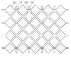
도 1 내지 도 4는 종래 정전용량 터치 패널의 개략도이다. 도 1과 도 3은 더블레이어(double-layer) 형태의 정전용량 터치 패널로서, 구동전극(110,310)과 인접한 구동전극(110,310)을 연결하여 연결된 구동전극(110,310)이 하나의 전극라인으로 형성되도록 하는 제1브릿지 전극(130,330)이 동일 평면 상에 형성된다.1 to 4 are schematic views of a conventional capacitive touch panel. 1 and 3 illustrate a double-layer capacitive touch panel, in which the
그리고, 절연막 개재하에 센싱전극(120,320)과 인접한 센싱전극(120,320)을 연결하여 하나의 전극라인으로 형성되도록 하는 제2브릿지 전극(140,340)을 형성한다.The
즉, 서로 다른 두 평면 상에 구동전극(110,310)과 센싱전극(120,320)이 형성되므로 이를 더블레이어(double-layer)라고 한다.That is, since the
또한, 도 2와 도 4는 싱글레이어(single-layer) 형태의 정전용량 터치 패널로서, 구동전극(210,410), 센싱전극(220,420) 및 구동전극(210,410)들이 하나의 전극라인으로 형성되도록 서로 전기적으로 연결되게 하는 제1브릿지 전극(230,430)을 형성한다.2 and 4 illustrate a single-layer capacitive touch panel, in which the driving
그리고, 배열된 방향에 따라 센싱전극(220,420)들이 하나의 전극라인으로 형성되도록 센싱전극(220,420)에 형성된 컨택홀을 통해 각 센싱전극(220,420)을 전기적으로 연결하는 제2브릿지 전극(240,440)을 형성한다.The
즉, 동일 평면 상에 구동전극(220,320)과 센싱전극(220,420)이 형성되므로 이를 싱글레이어(single-layer)라고 한다.That is, since the
그런데, 도 1과 도 2의 종래 정전용량 터치 패널은 각 전극의 형태가 마름모 형태로 형성되어 전극간 공간이 전체적으로 사선 형태로 형성됨에 따라, 대략 사각형인 단위 화소영역을 가지는 액정표시장치의 일 측면에 설치하여 사용하게 되는 경우, 전극간 공간이 외부에서 시인되는 문제점이 있었다.However, in the conventional capacitive touch panel of FIGS. 1 and 2, since each electrode is formed in a rhombus shape and the inter-electrode space is formed in an oblique shape as a whole, one side of the liquid crystal display having an approximately rectangular unit pixel area is formed. When installed in the use, there was a problem that the inter-electrode space is visually recognized from the outside.
또한, 도 3 및 도 4의 종래 정전용량 터치 패널은 각 전극의 형태가 대략 사각형태로 형성되어 전극간 공간이 액정표시장치의 화소영역과 대응되어 구동전극 또는 센싱전극이 외부에서 시인되는 문제점은 개선될 수 있으나, 구동전극에 인가되는 구동신호의 인가방향과 센싱되는 방향이 대각선으로 형성되어 통상 패널의 가로와 세로를 X축 및 Y축으로 하여 터치 위치를 검출하는 방법에 비해 검출 정확도가 저하되는 문제점이 있었다.In addition, the conventional capacitive touch panel of FIGS. 3 and 4 has a shape in which each electrode has a substantially rectangular shape, and thus the space between the electrodes corresponds to the pixel area of the liquid crystal display, so that the driving electrode or the sensing electrode is visually recognized from the outside. Although the direction in which the driving signal applied to the driving electrode is applied and the sensing direction are formed diagonally, the detection accuracy is lower than that of the method of detecting the touch position by using the horizontal and vertical axes of the panel as the X and Y axes. There was a problem.
불투명금속으로 제1브릿지 전극 또는 제2브릿지 전극을 형성하는 경우, 제1브릿지 전극 또는 제2브릿지 전극이 외부에서 시인될 수 있는데, 종래의 경우는 브릿지 전극의 개수가 많아서 시인성에 문제가 있었다.When the first bridge electrode or the second bridge electrode is formed of an opaque metal, the first bridge electrode or the second bridge electrode may be visually recognized from the outside. In the conventional case, the number of bridge electrodes is large, which causes a problem in visibility.
본 발명의 과제는 상술한 바와 같은 종래의 문제점을 해결하기 위한 것으로서, 구동전극 및 센싱전극으로 사용되는 전극의 형태를 적어도 하나의 화소영역과 대응되는 형태로 형성하여 전극의 시인성을 개선할 수 있는 정전용량 터치 패널 및 그 제조방법을 제공하는 것을 목적으로 한다.An object of the present invention is to solve the conventional problems as described above, by forming the shape of the electrode used as the driving electrode and the sensing electrode to correspond to the at least one pixel area to improve the visibility of the electrode An object of the present invention is to provide a capacitive touch panel and a method of manufacturing the same.
또한, 구동신호 방향과 센싱신호 방향을 패널을 기준으로 가로와 세로를 X축 및 Y축으로 하여 검출함으로써 터치 위치의 검출 정확도를 향상시킬 수 있는 정전용량 터치 패널 및 그 제조방법을 제공하는 것을 목적으로 한다.In addition, an object of the present invention is to provide a capacitive touch panel capable of improving the detection accuracy of a touch position by detecting the driving signal direction and the sensing signal direction on the X and Y axes of the panel. It is done.
상기 과제는, 본 발명에 따라, 제1방향 및 제2방향으로 교대배열되는 제1센싱전극과 제2센싱전극을 포함하고, 상기 제1센싱전극은 상기 제1방향을 따라 지그재그 형태로 전기적으로 연결되며, 상기 제2센싱전극은 상기 제2방향을 따라 지그재그 형태로 전기적으로 연결되는 것을 특징으로 하는 정전용량 터치패널에 의해 달성될 수 있다.According to the present invention, the object includes a first sensing electrode and a second sensing electrode alternately arranged in a first direction and a second direction, the first sensing electrode is electrically in a zigzag form along the first direction The second sensing electrode may be electrically connected in a zigzag form along the second direction.
여기서, 상기 제1센싱전극 및 제2센싱전극은 각각 제1브릿지 전극 및 제2브릿지전극에 의해 서로 전기적으로 연결될 수 있다.The first sensing electrode and the second sensing electrode may be electrically connected to each other by a first bridge electrode and a second bridge electrode, respectively.
또한, 상기 제1브릿지 전극 서로 인접한 제1센싱전극의 마주보는 영역을 전기적으로 연결하고, 상기 제2브릿지 전극은 서로 인접한 제2센싱전극의 마주보는 영역을 전기적으로 연결하도록 형성될 수 있다.In addition, the first bridge electrodes may be formed to electrically connect the facing regions of the first sensing electrodes adjacent to each other, and the second bridge electrode may be formed to electrically connect the facing regions of the second sensing electrodes adjacent to each other.
또한, 상기 제1센싱전극 및 상기 제2센싱전극은 절연막을 사이에 두고 서로 다른 평면에 형성될 수 있다.The first sensing electrode and the second sensing electrode may be formed on different planes with an insulating layer therebetween.
또한, 상기 제1센싱전극 및 상기 제2센싱전극은 동일 평면에 형성될 수 있다.In addition, the first sensing electrode and the second sensing electrode may be formed on the same plane.
또한, 상기 제1센싱전극 및 상기 제2센싱전극의 각 변은 상기 제1방향 및 상기 제2방향과 평행하게 형성될 수 있다.In addition, each side of the first sensing electrode and the second sensing electrode may be formed in parallel with the first direction and the second direction.
또한, 상기 제1센싱전극 및 상기 제2센싱전극의 각 변은 표시장치의 기판의 가로변 또는 세로변과 평행하게 형성될 수 있다.In addition, each side of the first sensing electrode and the second sensing electrode may be formed in parallel with the horizontal side or the vertical side of the substrate of the display device.
한편, 상기 정전용량 터치패널의 일 실시예에 따른 제조방법은, 기판 상에 투명도전막을 적층하고 패터닝하여 제1방향을 따라 지그재그 형태로 다수의 제1센싱전극이 배열되도록 하고, 상기 제1방향을 따라 인접한 상기 제1센싱전극을 서로 전기적으로 연결되도록 하는 제1브릿지 전극을 형성하는 단계; 상기 제1센싱전극과 상기 제1브릿지 전극이 형성된 기판 전면에 절연막을 형성하는 단계; 상기 절연막의 상부에 투명도전막을 적층하고 패터닝하여 상기 제2방향을 따라 지배열되도록 하되 상기 제1센싱전극과 상기 제1방향 및 상기 제2방향을 따라 교대배열되도록 하는 다수의 제2센싱전극과, 제2방향을 따라 인접한 상기 제2센싱전극을 서로 전기적으로 연결되도록 하는 제2브릿지 전극을 형성하는 단계; 상기 제2센싱전극 및 상기 제2브릿지 전극을 덮도록 오버코트층을 형성하는 단계;를 포함할 수 있다.Meanwhile, in the manufacturing method according to the embodiment of the capacitive touch panel, a plurality of first sensing electrodes are arranged in a zigzag form along a first direction by stacking and patterning a transparent conductive film on a substrate, and in the first direction. Forming a first bridge electrode to electrically connect the adjacent first sensing electrodes to each other; Forming an insulating film on an entire surface of the substrate on which the first sensing electrode and the first bridge electrode are formed; A plurality of second sensing electrodes stacked on the insulating layer and patterned so as to be dominantly arranged along the second direction, and alternately arranged along the first sensing electrode and the first and second directions; Forming a second bridge electrode electrically connecting the second sensing electrodes adjacent to each other along a second direction; And forming an overcoat layer to cover the second sensing electrode and the second bridge electrode.
상기 정전용량 터치패널의 다른 실시예에 따른 제조방법은, 기판 상에 투명도전막을 적층하고 패터닝하여 제1방향 및 제2방향으로 제1센싱전극과 제2센싱전극이 교대배열되도록 하고, 상기 제1방향을 따라 인접한 상기 제1센싱전극을 지그재그 형태로 서로 전기적으로 연결되게 하는 제1브릿지 전극을 형성하는 단계; 상기 제2센싱전극의 양측 일부를 노출시키는 컨택홀이 형성되며, 상기 제1센싱전극, 상기 제2센싱전극 및 상기 제1브릿지 전극을 덮는 절연막을 형성하는 단계; 상기 컨택홀을 통해 상기 제2방향을 따라 인접한 상기 제2센싱전극을 지그재그 형태로 서로 전기적으로 연결되게 하는 제2브릿지 전극을 형성하는 단계; 상기 제2브릿지 전극을 덮도록 오버코트층을 형성하는 단계;를 포함할 수 있다.According to another aspect of the present disclosure, a method of manufacturing a capacitive touch panel includes stacking and patterning a transparent conductive film on a substrate to alternately arrange a first sensing electrode and a second sensing electrode in a first direction and a second direction. Forming a first bridge electrode to electrically connect the first sensing electrodes adjacent to each other along the one direction in a zigzag form; Forming a contact hole for exposing a portion of both sides of the second sensing electrode and covering the first sensing electrode, the second sensing electrode, and the first bridge electrode; Forming a second bridge electrode electrically connecting the second sensing electrodes adjacent to each other in the second direction through the contact hole in a zigzag form; And forming an overcoat layer to cover the second bridge electrode.
상기 정전용량 터치패널의 또 다른 실시예에 따른 제조방법은, 기판 상에 제1방향을 따라 일정간격으로 제1브릿지 전극을 형성하고, 상기 제1브릿지 전극의 상기 제1방향을 기준으로 양측 일부를 노출시키는 컨택홀이 형성된 절연막을 상기 제1브릿지 전극의 상부를 덮도록 형성하는 단계; 상기 절연막의 상부에 투명도전막을 적층하고 패터닝하여 상기 컨택홀을 통해 상기 제1브릿지 전극과 연결되어 상기 제1방향을 따라 지그재그 형태로 전기적으로 연결되는 다수의 제1센싱전극과, 상기 제1센싱전극과 상기 제1방향 및 상기 제2방향으로 교대배열되도록 형성되는 다수의 제2센싱전극과, 상기 제2방향을 따라 인접한 상기 제2센싱전극을 지그재그 형태로 서로 전기적으로 연결되게 하는 제2브릿지 전극을 형성하는 단계; 상기 제1센싱전극, 상기 제2센싱전극 및 상기 제2브릿지 전극을 덮도록 오버코트층을 형성하는 단계;를 포함할 수 있다.In another embodiment of the capacitive touch panel, a first bridge electrode may be formed on a substrate at a predetermined interval along a first direction, and may be partially formed on both sides of the first bridge electrode based on the first direction. Forming an insulating film having a contact hole exposing the upper surface of the first bridge electrode; A plurality of first sensing electrodes connected to the first bridge electrode through the contact hole and electrically connected in a zigzag shape along the first direction by stacking and patterning a transparent conductive film on the insulating layer; A second bridge for electrically connecting the electrodes, the plurality of second sensing electrodes formed to be alternately arranged in the first direction and the second direction, and the second sensing electrodes adjacent to each other in the second direction in a zigzag form. Forming an electrode; And forming an overcoat layer to cover the first sensing electrode, the second sensing electrode, and the second bridge electrode.
여기서, 상기 제1센싱전극 및 상기 제2센싱전극의 각 변은 상기 제1방향 및 상기 제2방향과 평행하게 형성할 수 있다.Here, each side of the first sensing electrode and the second sensing electrode may be formed in parallel with the first direction and the second direction.
또한, 상기 제1센싱전극 및 상기 제2센싱전극의 각 변은 패널의 가로변 또는 세로변과 평행하게 형성할 수 있다.In addition, each side of the first sensing electrode and the second sensing electrode may be formed parallel to the horizontal side or the vertical side of the panel.
본 발명에 따르면, 구동전극 및 센싱전극으로 사용되는 전극의 형태를 적어도 하나의 화소영역과 대응되는 형태로 형성하여 전극의 시인성을 개선할 수 있는 정전용량 터치 패널 및 그 제조방법이 제공된다.According to the present invention, there is provided a capacitive touch panel and a method of manufacturing the same, which improve the visibility of the electrode by forming the shape of the electrode used as the driving electrode and the sensing electrode to correspond to at least one pixel area.
또한, 구동신호 방향과 센싱신호 방향을 패널을 기준으로 가로와 세로를 X축 및 Y축으로 하여 검출함으로써 터치 위치의 검출 정확도를 향상시킬 수 있는 정전용량 터치 패널 및 그 제조방법이 제공된다.In addition, a capacitive touch panel and a method of manufacturing the same are provided which can improve the detection accuracy of the touch position by detecting the driving signal direction and the sensing signal direction on the X and Y axes of the panel.
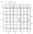
도 1 내지 도 4는 종래 정전용량 터치 패널의 개략도,
도 5는 본 발명의 제1실시예에 따른 정전용량 터치 패널의 개략도,
도 6은 도 5의 A-A'을 따라 절단한 단면도,
도 7은 도 5의 센싱도이다.
도 8은 본 발명의 제2실시예에 따른 정전용량 터치 패널의 개략도,
도 9는 도 8의 B-B'을 따라 절단한 단면도,
도 10은 본 발명의 제3실시예에 따른 정전용량 터치 패널의 단면도이다.1 to 4 are schematic views of a conventional capacitive touch panel,
5 is a schematic diagram of a capacitive touch panel according to a first embodiment of the present invention;
6 is a cross-sectional view taken along line AA ′ of FIG. 5;
7 is a sensing diagram of FIG. 5.
8 is a schematic diagram of a capacitive touch panel according to a second embodiment of the present invention;
FIG. 9 is a cross-sectional view taken along line BB ′ of FIG. 8;
10 is a cross-sectional view of a capacitive touch panel according to a third embodiment of the present invention.
설명에 앞서, 여러 실시예에 있어서, 동일한 구성을 가지는 구성요소에 대해서는 동일한 부호를 사용하여 대표적으로 제1실시예에서 설명하고, 그 외의 실시예에서는 제1실시예와 다른 구성에 대해서 설명하기로 한다.Prior to the description, components having the same configuration are denoted by the same reference numerals as those in the first embodiment. In other embodiments, configurations different from those of the first embodiment will be described do.
본 발명에 따른 정전용량 터치 패널은 표시장치 또는 액정표시장치의 기판에 형성될 수 있으며, 제1방향 및 제2방향으로 교대배열되는 제1센싱전극과 제2센싱전극을 포함할 수 있다.The capacitive touch panel according to the present invention may be formed on a substrate of a display device or a liquid crystal display, and may include a first sensing electrode and a second sensing electrode that are alternately arranged in a first direction and a second direction.
이때, 제1센싱전극은 제1브릿지 전극을 통해 제1방향을 따라 지그재그(jig-jag)형태로 서로 전기적으로 연결될 수 있고, 제2센싱전극은 제2브릿지 전극을 통해 제2방향을 따라 지그재그(jig-jag)형태로 서로 전기적으로 연결될 수 있다.In this case, the first sensing electrodes may be electrically connected to each other in a jig-jag shape along the first direction through the first bridge electrode, and the second sensing electrodes may be zig-zag along the second direction through the second bridge electrode. (jig-jag) can be electrically connected to each other.
여기서, 제1방향과 제2방향은 표시장치인 경우 기판의 X축 방향, Y축 방향일 수 있고, 액정표시장치인 경우 게이트라인 방향과 데이터라인 방향일 수 있다.Here, the first direction and the second direction may be the X-axis direction and the Y-axis direction of the substrate in the case of a display device, and may be the gate line direction and the data line direction in a liquid crystal display device.
후술하는 실시예들에서는 정전용량 터치패널이 액정표시장치의 기판에 형성되는 경우를 예를 들어 설명하기로 한다.In the following embodiments, a case in which the capacitive touch panel is formed on the substrate of the liquid crystal display will be described.
이하, 첨부한 도면을 참조하여 본 발명의 제1실시예에 따른 정전용량 터치 패널에 대하여 상세하게 설명한다.Hereinafter, a capacitive touch panel according to a first embodiment of the present invention will be described in detail with reference to the accompanying drawings.
도 5는 본 발명의 제1실시예에 따른 정전용량 터치 패널의 개략도이고, 도 6은 도 5의 A-A'을 따라 절단한 단면도이다.5 is a schematic view of a capacitive touch panel according to a first embodiment of the present invention, and FIG. 6 is a cross-sectional view taken along line AA ′ of FIG. 5.
도 5 및 도 6을 참조하면, 본 발명의 제1실시예에 따른 정전용량 터치 패널(1)은 제1센싱전극과 제2센싱전극이 서로 다른 평면 즉, 더블 레이어(double layer)형태이며, 제1센싱전극(10), 제1브릿지 전극(20), 절연막(30), 제2센싱전극(40), 제2브릿지 전극(50) 및 오버코트층(60)을 포함하여 구성될 수 있다.5 and 6, the
상기 제1센싱전극(10)은 기판(2) 상에 게이트라인 및 데이터라인 방향의 변을 가진 대략 사각형 형태를 가지도록 형성되며, 게이트라인을 따라 지그재그(jig-jag) 형태로 배열될 수 있다.The
상기 제1브릿지 전극(20)은 게이트라인 방향으로 지그재그형태로 배열된 인접한 제1센싱전극(10)을 서로 전기적으로 연결하도록 형성될 수 있다.The
여기서, 제1브릿지 전극(20)은 인접한 두 제1센싱전극(10)의 마주보는 영역 구체적으로는 마주보는 두 모서리영역을 전기적으로 연결하도록 형성될 수 있다.Here, the
상기 절연막(30)은 상기 제1센싱전극(10) 및 제1브릿지 전극(20)의 상부를 덮도록 형성될 수 있다.The insulating
상기 제2센싱전극(40)은 제1센싱전극(10)과 실질적으로 동일한 형태 또는 대응되는 형태로 절연막(30)의 상부에 데이터라인 방향을 따라 지그재그 형태로 배열되어 제1센싱전극과 함께 게이트라인 방향 및 데이터라인 방향으로 교대배열되도록 형성될 수 있다.The
상기 제2브릿지 전극(50)은 데이터라인 방향으로 지그재그형태로 배열된 인접한 제2센싱전극(40)을 전기적으로 연결하도록 형성될 수 있다.The
여기서, 제2브릿지 전극(50)은 인접한 두 제2센싱전극(40)의 마주보는 영역 구체적으로는 마주보는 두 모서리영역을 전기적으로 연결하도록 형성될 수 있다.Here, the
상기 오버코트층(60)은 제2센싱전극(40)과 제2브릿지 전극(50)을 덮도록 형성될 수 있다.The
한편, 제1센싱전극(10)과 제2센싱전극(40)의 각 변은 액정표시장치의 가로변과 평행한 게이트라인 방향 및 세로변과 평행한 데이터라인 방향과 평행하게 형성될 수 있다.Each side of the
즉, 제1센싱전극(10)과 제2센싱전극(40)을 적어도 하나의 화소영역과 실질적으로 일치하는 크기로 형성하면 센싱전극의 시인성을 개선할 수 있다.
That is, when the
상술한 바와 같은 정전용량 터치 패널(1)에서 터치위치에 대한 센싱방법은, 제1센싱전극(10)은 순차적으로 구동신호를 인가되도록 연결하고, 제2센싱전극(40)은 동시에 구동되도록 연결하여, 제1센싱전극(10)과 제2센싱전극(40) 사이의 정전용량을 감지하여 터치에 대한 센싱을 할 수 있다.In the
다른 방법으로는, 제1센싱전극(10)과 제2센싱전극(40)의 각각의 방향으로 신호를 인가한 후, 출력되는 신호의 변화를 감지하여 터치 위치를 검출할 수도 있다.Alternatively, the touch position may be detected by applying a signal in each direction of the
이와 같은 방법에서 센싱방향은, 도 7에서와 같이, 제1센싱전극(10)의 센싱방향과 게이트라인 방향이 일치하고, 제2센싱전극(40)의 센싱방향과 데이터라인 방향이 일치할 수 있다.In this manner, as illustrated in FIG. 7, the sensing direction of the
결과적으로, 구동방향 및 센싱방향이 액정표시장치의 화소구조의 배열형태와 일치할 수 있어 터치 위치의 검출 정확도가 향상될 수 있다.
As a result, the driving direction and the sensing direction can coincide with the arrangement of the pixel structure of the liquid crystal display device, so that the accuracy of detecting the touch position can be improved.
상술한 바와 같은 본 발명의 제1실시예에 따른 정전용량 터치 패널의 제조방법에 대해 설명한다.A method of manufacturing the capacitive touch panel according to the first embodiment of the present invention as described above will be described.
먼저, 기판(2) 상에 투명도전막을 형성하고 공지의 패터닝 공정을 통해 패터닝하여 게이트라인 방향을 따라 지그재그형태로 제1센싱전극(10)을 배열하고, 게이트라인 방향을 따라 인접한 제1센싱전극(10)을 전기적으로 연결하는 제1브릿지 전극(20)을 형성한다.First, a transparent conductive film is formed on the
그리고, 제1센싱전극(10) 및 제1브릿지 전극(20)의 상부를 덮도록 절연재질의 절연막(30)을 형성한다.The insulating
이어, 절연막(30)의 상부에 투명도전막을 형성한 후 공지의 패터닝 공정을 통해 패터닝하여 데이터라인 방향으로 지그재그형태로 형성하여, 제1센싱전극(10)과 게이트라인 방향 및 데이터라인 방향으로 제2센싱전극(40)을 교대배열되도록 하고, 데이터라인 방향으로 인접한 제2센싱전극(40)을 서로 전기적으로 연결되도록 하는 제2브릿지 전극(50)을 형성한다.Subsequently, a transparent conductive film is formed on the insulating
그리고, 제2센싱전극(40)이 형성된 기판(2) 전면에 오버코트층(60)을 형성하여 제조를 완료할 수 있다.
In addition, the
도 8은 본 발명의 제2실시예에 따른 정전용량 터치 패널의 개략도이고, 도 9는 도 8의 B-B'을 따라 절단한 단면도이다. 본 발명의 제2실시예는 제1실시예의 더블 레이어(double layer)형태인 것과는 달리, 제1센싱전극과 제2센싱전극이 동일 평면 즉, 싱글 레이어(single layer) 형태로 형성될 수 있다.8 is a schematic view of a capacitive touch panel according to a second embodiment of the present invention, and FIG. 9 is a cross-sectional view taken along line BB ′ of FIG. 8. In the second embodiment of the present invention, unlike the double layer type of the first embodiment, the first sensing electrode and the second sensing electrode may be formed in the same plane, that is, in the form of a single layer.
도 8과 도 9를 참조하면, 본 발명의 제2실시예에 따른 정전용량 터치 패널(1A)은 제1실시예에서와 같이 제1센싱전극(10), 제1브릿지 전극(20), 절연막(30), 제2센싱전극(40), 제2브릿지 전극(50) 및 오버코트층(60)을 포함하여 구성될 수 있다.8 and 9, the
상기 제1센싱전극(10)과 제2센싱전극(40)은 기판(2) 상에 제1실시예에서와 같이 각각 게이트라인 방향 또는 데이터라인 방향으로 지그재그 형태로 배열되되, 교대로 배열될 수 있다.The
또한, 제1센싱전극(10)과 제2센싱전극(40)의 형태는 게이트라인 방향 및 데이터라인 방향과 실질적으로 일치하는 두 변을 가지는 대략 사각형 형태로 형성될 수 있다.In addition, the
상기 제1브릿지 전극(20)은 기판(2) 상에 형성되며, 게이트라인 방향으로 배열된 인접한 제1센싱전극(10)을 서로 전기적으로 연결되도록 형성될 수 있다.The
상기 절연막(30)은 제1센싱전극(10), 제2센싱전극(40) 및 제1브릿지 전극(20)의 상부를 덮도록 형성될 수 있다.The insulating
이때, 절연막(30)에는 데이터라인 방향으로 배열된 제2센싱전극(40)의 양측 일부를 노출시키는 컨택홀(미도시)이 형성될 수 있으며, 컨택홀의 위치는 데이터라인 방향으로 양측 가장자리 바람직하게는 데이터라인 방향으로 인접한 두 제2센싱전극의 양측 모서리 영역일 수 있다.In this case, a contact hole (not shown) may be formed in the insulating
상기 제2브릿지 전극(50)은 절연막(30)의 상부에 형성되며, 컨택홀을 통해 데이터라인 방향으로 지그재그 형태로 배열되는 서로 인접한 제2센싱전극(40)을 상호 전기적으로 연결되게 할 수 있다.The
상기 오버코트층(60)은 제2브릿지 전극(50)의 상부를 덮도록 형성될 수 있다.The
상술한 바와 같은 본 발명의 제2실시예에 따른 정전용량 터치 패널의 제조방법에 대해 설명한다.A method of manufacturing the capacitive touch panel according to the second embodiment of the present invention as described above will be described.
먼저, 기판(2) 상에 투명도전막을 형성하고 공지의 패터닝공정을 통해 패터닝하여 게이트라인 방향으로 제1센싱전극(10)이 지그재그 형태로 배열되도록 하고, 데이터라인 방향으로 제2센싱전극(40)을 지그재그 형태로 배열되도록 하여 제1센싱전극(10)과 제2센싱전극(40)이 게이트라인 및 데이터라인 방향으로 교대배열되도록 한다.First, a transparent conductive film is formed on the
이와 동시에, 게이트라인 방향으로 배열되는 제1센싱전극(10)을 전기적으로 연결되게 하는 제1브릿지 전극(20)을 형성한다.At the same time, the
그리고, 제1센싱전극(10), 제2센싱전극(40) 및 제1브릿지 전극(20)이 형성된 기판(2) 전면에 절연막(30)을 형성하고, 소정의 식각 등의 방법으로 데이터라인 방향으로 배열된 제2센싱전극(40)의 상하 양측 일부를 노출시키는 컨택홀을 형성한다.Then, an insulating
이때, 컨택홀 형성위치는 데이터라인 방향으로 지그재그 형태로 배열되는 제2센싱전극(40)의 마주보는 영역일 수 있으며, 바람직하게는 마주보는 모서리 영역일 수 있다.In this case, the contact hole formation position may be an area facing the
이어, 컨택홀이 형성된 절연막(30)의 상부에 도전막을 형성하고, 공지의 패터닝공정을 통해 패터닝하여 컨택홀을 통해 데이터라인 방향으로 배열되는 인접한 제2센싱전극(40)들이 전기적으로 연결되도록 하는 제2브릿지 전극(50)을 형성한다.Subsequently, a conductive film is formed on the insulating
그리고, 제2브릿지 전극(50)이 형성된 기판(2) 전면에 오버코트층(60)을 형성하여 제조를 완료할 수 있다.
In addition, the
다음으로, 본 발명의 제3실시예에 따른 정전용량 터치 패널에 대해 설명한다. 제3실시예는 제2실시예와 같이 싱글레이어(single layer) 형태이나 제2실시예와는 다른 구조이다.Next, a capacitive touch panel according to a third embodiment of the present invention will be described. The third embodiment has a single layer form like the second embodiment, but has a different structure from the second embodiment.
도 10은 본 발명의 제3실시예에 따른 정전용량 터치 패널의 단면도이다.10 is a cross-sectional view of a capacitive touch panel according to a third embodiment of the present invention.
도 10을 참조하면, 본 발명의 제3실시예에 따른 정전용량 터치 패널(1B)은 제2실시예에서와 같이 제1센싱전극(10), 제1브릿지 전극(20), 절연막(30), 제2센싱전극(40), 제2브릿지 전극(50) 및 오버코트층(60)을 포함하여 구성될 수 있다.Referring to FIG. 10, the capacitive touch panel 1B according to the third embodiment of the present invention may include the
제3실시예에서는 제1브릿지 전극(20)이 기판(2)의 상부에 먼저 형성되고, 그 상부에 제1브릿지 전극(20)의 게이트라인 방향의 양측 일부를 노출시키는 컨택홀이 형성된 절연막(30)이 형성될 수 있다.In the third embodiment, the
그리고, 절연막(30)의 상부에 제1센싱전극(10)과 제2센싱전극(40) 및 제2브릿지 전극(50)이 형성될 수 있다.In addition, the
제1센싱전극(10)은 게이트라인 방향으로 지그재그 형태로 배열되며, 컨택홀을 통해 제1브릿지 전극과 연결되어 게이트라인 방향으로 인접한 제1센싱전극(10)들이 전기적으로 연결될 수 있다.The
제2센싱전극은(40)은 데이터라인 방향으로 지그재그 형태로 배열되어 제1센싱전극(10)과 함께 게이트라인 및 데이터라인 방향으로 교대배열될 수 있다.The
제2브릿지 전극(50)은 데이터라인 방향으로 배열되는 인접한 제2센싱전극(40)이 전기적으로 연결되도록 형성될 수 있다.The
상술한 본 발명의 제3실시예에 따른 정전용량 터치 패널의 제조방법에 대해 설명한다.A method of manufacturing the capacitive touch panel according to the third embodiment of the present invention described above will be described.
먼저, 기판(2) 상에 금속 등의 도전막을 형성하고 공지의 패터닝 공정을 통해 게이트라인 방향을 따라 일정간격으로 제1브릿지 전극(20)을 형성한다.First, a conductive film such as metal is formed on the
그리고, 제1브릿지 전극(20)이 형성된 기판(2) 전면에 절연막(30)을 형성하고, 소정의 식각 등의 공정을 통해 절연막(30)에 제1브릿지 전극(20)의 양측 일부를 각각 노출시키는 컨택홀을 형성한다.In addition, an insulating
이어, 절연막(30)의 상부에 투명도전막을 형성하고, 공지의 패터닝공정을 통해 패터닝하여 제1센싱전극(10)과 제2센싱전극(40) 및 제2브릿지 전극(50)을 형성한다.Subsequently, a transparent conductive film is formed on the insulating
이때, 제1센싱전극(10)은 게이트라인 방향으로 지그재그 형태로 배열되도록 하고, 제2센싱전극(40)은 데이터라인 방향으로 지그재그 형태로 배열되도록 하여, 제1센싱전극(10)과 제2센싱전극(40)이 게이트라인 및 데이터라인 방향으로 교대배열되도록 형성한다.In this case, the
또한, 제1센싱전극(10)은 절연막(30)에 형성된 컨택홀을 통해 제1브릿지 전극(20)과 연결되도록 하여 게이트라인 방향으로 인접한 제1센싱전극(10)이 서로 전기적으로 연결되도록 형성한다.In addition, the
아울러, 제2브릿지 전극(50)은 데이터라인 방향으로 배열된 인접한 제2센싱전극(40)들을 전기적으로 연결되도록 형성한다.In addition, the
그리고, 제1센싱전극(10), 제2센싱전극(40) 및 제2브릿지 전극(50)이 형성된 기판(2) 전면에 오버코트층(60)을 형성하여 제조를 완료한다.In addition, an
상술한 바와 같은 본 발명의 실시예들에 따른 정전용량 터치 패널은 센싱전극들의 형태가 화소구조와 실질적으로 일치될 수 있어 시인성이 개선될 수 있고, 구동신호 방향 및 센싱신호 방향을 액정표시장치의 게이트라인 및 데이터라인 방향과 실질적으로 일치되게 할 수 있어 검출정확도가 향상될 수 있다.As described above, in the capacitive touch panel according to the embodiments of the present invention, the shape of the sensing electrodes may substantially match the pixel structure, so that the visibility may be improved, and the driving signal direction and the sensing signal direction may be changed to The detection accuracy can be improved by being substantially coincident with the gate line and data line directions.
상술한 본 발명의 실시예들에서는 액정표시장치의 기판에 형성되는 형태를 예를 들어 설명하였으며, 실질적으로 일반적인 표시장치에 적용되는 경우에도 표시장치를 기준으로 가로와 세로를 X축 및 Y축으로 하여 검출함으로써 검출정확도가 향상될 수 있다.In the above-described embodiments of the present invention, the form formed on the substrate of the liquid crystal display device has been described as an example. Detection accuracy can be improved.
본 발명의 권리범위는 상술한 실시예에 한정되는 것이 아니라 첨부된 특허청구범위 내에서 다양한 형태의 실시예로 구현될 수 있다. 특허청구범위에서 청구하는 본 발명의 요지를 벗어남이 없이 당해 발명이 속하는 기술 분야에서 통상의 지식을 가진 자라면 누구든지 변형 가능한 다양한 범위까지 본 발명의 청구범위 기재의 범위 내에 있는 것으로 본다.The scope of the present invention is not limited to the above-described embodiments, but may be embodied in various forms of embodiments within the scope of the appended claims. Without departing from the gist of the invention claimed in the claims, it is intended that any person skilled in the art to which the present invention pertains falls within the scope of the claims described in the present invention to various extents which can be modified.
※도면의 주요 부분에 대한 부호의 설명※
10 : 제1센싱전극20 : 제1브릿지 전극30 : 절연막
40 : 제2센싱전극50 : 제2브릿지 전극60 : 오버코트층※ Explanation of code for main part of drawing ※
DESCRIPTION OF
40: second sensing electrode 50: second bridge electrode 60: overcoat layer
Claims (12)
Translated fromKorean상기 제1센싱전극 및 제2센싱전극은 각각 제1브릿지 전극 및 제2브릿지전극에 의해 서로 전기적으로 연결되는 것을 특징으로 하는 정전용량 터치패널.The method of claim 1,
And the first sensing electrode and the second sensing electrode are electrically connected to each other by a first bridge electrode and a second bridge electrode, respectively.
상기 제1브릿지 전극 서로 인접한 제1센싱전극의 마주보는 영역을 전기적으로 연결하고, 상기 제2브릿지 전극은 서로 인접한 제2센싱전극의 마주보는 영역을 전기적으로 연결하도록 형성되는 것을 특징으로 하는 정전용량 터치패널.The method of claim 2,
The first bridge electrode is configured to electrically connect the facing areas of the first sensing electrodes adjacent to each other, and the second bridge electrode is formed to electrically connect the facing areas of the second sensing electrodes adjacent to each other. Touch panel.
상기 제1센싱전극 및 상기 제2센싱전극은 절연막을 사이에 두고 서로 다른 평면에 형성되는 것을 특징으로 하는 정전용량 터치패널.The method of claim 2,
And the first sensing electrode and the second sensing electrode are formed on different planes with an insulating layer therebetween.
상기 제1센싱전극 및 상기 제2센싱전극은 동일 평면에 형성되는 것을 특징으로 하는 정전용량 터치패널.The method of claim 2,
And the first sensing electrode and the second sensing electrode are formed on the same plane.
상기 제1센싱전극 및 상기 제2센싱전극의 각 변은 상기 제1방향 및 상기 제2방향과 평행하게 형성되는 것을 특징으로 하는 정전용량 터치패널.The method according to any one of claims 1 to 5,
Each side of the first sensing electrode and the second sensing electrode, the capacitive touch panel, characterized in that formed in parallel with the first direction and the second direction.
상기 제1센싱전극 및 상기 제2센싱전극의 각 변은 표시장치의 기판의 가로변 또는 세로변과 평행하게 형성되는 것을 특징으로 하는 정전용량 터치패널.The method according to any one of claims 1 to 5,
Each side of the first sensing electrode and the second sensing electrode, the capacitive touch panel, characterized in that formed in parallel with the horizontal side or the vertical side of the substrate of the display device.
상기 제1센싱전극과 상기 제1브릿지 전극이 형성된 기판 전면에 절연막을 형성하는 단계;
상기 절연막의 상부에 투명도전막을 적층하고 패터닝하여 제2방향을 따라 지배열되도록 하되 상기 제1센싱전극과 상기 제1방향 및 상기 제2방향을 따라 교대배열되도록 하는 다수의 제2센싱전극과, 상기 제2방향을 따라 인접한 상기 제2센싱전극을 서로 전기적으로 연결되도록 하는 제2브릿지 전극을 형성하는 단계;
상기 제2센싱전극 및 상기 제2브릿지 전극을 덮도록 오버코트층을 형성하는 단계;를 포함하는 것을 특징으로 하는 정전용량 터치패널의 제조방법.Stacking and patterning a transparent conductive film on a substrate so that a plurality of first sensing electrodes are arranged in a zigzag form along a first direction, and the first sensing electrodes are electrically connected to each other along the first direction. Forming a bridge electrode;
Forming an insulating film on an entire surface of the substrate on which the first sensing electrode and the first bridge electrode are formed;
A plurality of second sensing electrodes stacked on the insulating film and patterned so as to be dominantly arranged along a second direction, but alternately arranged along the first sensing electrode and the first and second directions; Forming a second bridge electrode electrically connecting the second sensing electrodes adjacent to each other along the second direction;
And forming an overcoat layer to cover the second sensing electrode and the second bridge electrode.
상기 제2센싱전극의 양측 일부를 노출시키는 컨택홀이 형성되며, 상기 제1센싱전극, 상기 제2센싱전극 및 상기 제1브릿지 전극을 덮는 절연막을 형성하는 단계;
상기 컨택홀을 통해 상기 제2방향을 따라 인접한 상기 제2센싱전극을 지그재그 형태로 서로 전기적으로 연결되게 하는 제2브릿지 전극을 형성하는 단계;
상기 제2브릿지 전극을 덮도록 오버코트층을 형성하는 단계;를 포함하는 것을 특징으로 하는 정전용량 터치패널의 제조방법.Laminating and patterning the transparent conductive film on the substrate so that the first sensing electrode and the second sensing electrode are alternately arranged in the first and second directions, and the first sensing electrodes adjacent to each other in the first direction are zigzag-shaped to each other. Forming a first bridge electrode to be electrically connected;
Forming a contact hole for exposing a portion of both sides of the second sensing electrode and covering the first sensing electrode, the second sensing electrode, and the first bridge electrode;
Forming a second bridge electrode electrically connecting the second sensing electrodes adjacent to each other in the second direction through the contact hole in a zigzag form;
Forming an overcoat layer to cover the second bridge electrode; manufacturing method of a capacitive touch panel comprising a.
상기 절연막의 상부에 투명도전막을 적층하고 패터닝하여 상기 컨택홀을 통해 상기 제1브릿지 전극과 연결되어 상기 제1방향을 따라 지그재그 형태로 전기적으로 연결되는 다수의 제1센싱전극과, 상기 제1센싱전극과 상기 제1방향 및 상기 제2방향으로 교대배열되는 다수의 제2센싱전극과, 상기 제2방향을 따라 인접한 상기 제2센싱전극을 지그재그 형태로 서로 전기적으로 연결되게 하는 제2브릿지 전극을 형성하는 단계;
상기 제1센싱전극, 상기 제2센싱전극 및 상기 제2브릿지 전극을 덮도록 오버코트층을 형성하는 단계;를 포함하는 것을 특징으로 하는 정전용량 터치패널의 제조방법.An insulating film is formed on the substrate to form a first bridge electrode at a predetermined interval along a first direction, and a contact hole is formed to expose a portion of both sides of the first bridge electrode based on a first direction of the first bridge electrode. Forming to cover;
A plurality of first sensing electrodes connected to the first bridge electrode through the contact hole and electrically connected in a zigzag shape along the first direction by stacking and patterning a transparent conductive film on the insulating layer; A plurality of second sensing electrodes alternately arranged in the first direction and the second direction, and a second bridge electrode which electrically connects the second sensing electrodes adjacent to each other in the second direction in a zigzag form. Forming;
And forming an overcoat layer to cover the first sensing electrode, the second sensing electrode, and the second bridge electrode.
상기 제1센싱전극 및 상기 제2센싱전극의 각 변은 상기 제1방향 및 상기 제2방향과 평행하게 형성하는 것을 특징으로 하는 정전용량 터치패널의 제조방법.The method according to any one of claims 8 to 10,
Each side of the first sensing electrode and the second sensing electrode is formed in parallel with the first direction and the second direction manufacturing method of the capacitive touch panel.
상기 제1센싱전극 및 상기 제2센싱전극의 각 변은 패널의 가로변 또는 세로변과 평행하게 형성하는 것을 특징으로 하는 정전용량 터치패널의 제조방법.The method according to any one of claims 8 to 10,
And each side of the first sensing electrode and the second sensing electrode is formed in parallel with a horizontal side or a vertical side of the panel.
Priority Applications (1)
| Application Number | Priority Date | Filing Date | Title |
|---|---|---|---|
| KR1020110019416AKR20120100488A (en) | 2011-03-04 | 2011-03-04 | Capacitance touch panel and the method thereof |
Applications Claiming Priority (1)
| Application Number | Priority Date | Filing Date | Title |
|---|---|---|---|
| KR1020110019416AKR20120100488A (en) | 2011-03-04 | 2011-03-04 | Capacitance touch panel and the method thereof |
Publications (1)
| Publication Number | Publication Date |
|---|---|
| KR20120100488Atrue KR20120100488A (en) | 2012-09-12 |
Family
ID=47110206
Family Applications (1)
| Application Number | Title | Priority Date | Filing Date |
|---|---|---|---|
| KR1020110019416ACeasedKR20120100488A (en) | 2011-03-04 | 2011-03-04 | Capacitance touch panel and the method thereof |
Country Status (1)
| Country | Link |
|---|---|
| KR (1) | KR20120100488A (en) |
Cited By (9)
| Publication number | Priority date | Publication date | Assignee | Title |
|---|---|---|---|---|
| KR20140126287A (en)* | 2013-03-25 | 2014-10-30 | 허페이 비오이 옵토일렉트로닉스 테크놀로지 컴퍼니 리미티드 | Capacitive in-cell touch panel and display device |
| CN104866131A (en)* | 2014-02-26 | 2015-08-26 | 海帝士科技公司 | Matrix switching type touch panel |
| WO2018119881A1 (en)* | 2016-12-26 | 2018-07-05 | 武汉华星光电技术有限公司 | Touch-control electrode and method for fabricating same |
| EP3293614A4 (en)* | 2015-05-05 | 2019-01-02 | Boe Technology Group Co. Ltd. | Touch display panel and drive method therefor, and touch display device |
| CN110231884A (en)* | 2013-08-16 | 2019-09-13 | 苹果公司 | The touch pad electrode structure of correction is grounded for user |
| KR20200126471A (en)* | 2019-04-29 | 2020-11-09 | 삼성디스플레이 주식회사 | Input sensing circuit and display module having the same |
| WO2022035165A1 (en)* | 2020-08-12 | 2022-02-17 | 동우 화인켐 주식회사 | Touch sensor, window laminate comprising same and image display device comprising same |
| US12014003B2 (en) | 2015-02-02 | 2024-06-18 | Apple Inc. | Flexible self-capacitance and mutual capacitance touch sensing system architecture |
| US12189899B2 (en) | 2019-09-06 | 2025-01-07 | Apple Inc. | Touch sensing with water rejection |
- 2011
- 2011-03-04KRKR1020110019416Apatent/KR20120100488A/ennot_activeCeased
Cited By (14)
| Publication number | Priority date | Publication date | Assignee | Title |
|---|---|---|---|---|
| US9665203B2 (en) | 2013-03-25 | 2017-05-30 | Hefei Boe Optoelectronics Technology Co., Ltd | Capacitive in-cell touch panel and display device |
| KR20140126287A (en)* | 2013-03-25 | 2014-10-30 | 허페이 비오이 옵토일렉트로닉스 테크놀로지 컴퍼니 리미티드 | Capacitive in-cell touch panel and display device |
| CN110231884B (en)* | 2013-08-16 | 2023-07-04 | 苹果公司 | Touch panel electrode structure for user ground correction |
| CN110231884A (en)* | 2013-08-16 | 2019-09-13 | 苹果公司 | The touch pad electrode structure of correction is grounded for user |
| CN104866131A (en)* | 2014-02-26 | 2015-08-26 | 海帝士科技公司 | Matrix switching type touch panel |
| CN104866131B (en)* | 2014-02-26 | 2018-09-25 | 海帝士科技公司 | Inverse problem formula touch panel |
| US12014003B2 (en) | 2015-02-02 | 2024-06-18 | Apple Inc. | Flexible self-capacitance and mutual capacitance touch sensing system architecture |
| EP3293614A4 (en)* | 2015-05-05 | 2019-01-02 | Boe Technology Group Co. Ltd. | Touch display panel and drive method therefor, and touch display device |
| US10216341B2 (en) | 2015-05-05 | 2019-02-26 | Boe Technology Group Co., Ltd. | Touch display panel, driving method for the same and touch display device |
| WO2018119881A1 (en)* | 2016-12-26 | 2018-07-05 | 武汉华星光电技术有限公司 | Touch-control electrode and method for fabricating same |
| KR20200126471A (en)* | 2019-04-29 | 2020-11-09 | 삼성디스플레이 주식회사 | Input sensing circuit and display module having the same |
| US12189899B2 (en) | 2019-09-06 | 2025-01-07 | Apple Inc. | Touch sensing with water rejection |
| WO2022035165A1 (en)* | 2020-08-12 | 2022-02-17 | 동우 화인켐 주식회사 | Touch sensor, window laminate comprising same and image display device comprising same |
| US12210710B2 (en) | 2020-08-12 | 2025-01-28 | Dongwoo Fine-Chem Co., Ltd | Touch sensor, window laminate comprising same and image display device comprising same |
Similar Documents
| Publication | Publication Date | Title |
|---|---|---|
| KR20120100488A (en) | Capacitance touch panel and the method thereof | |
| KR101040881B1 (en) | Touch screen panel | |
| CN103150070B (en) | A kind of capacitance touching control module, capacitance type in-cell touch panel and display device | |
| KR101530794B1 (en) | 3d touch control liquid crystal lens grating, method for manufacturing the same and 3d touch control display device | |
| WO2015196712A1 (en) | Touch display panel and display device | |
| KR101212420B1 (en) | Liquid crystal display apparatus with in-cell touch sensor and manufacturing method thereof | |
| KR20120036521A (en) | Liquid crystal display device | |
| JP2016146202A (en) | Touch panel and display device | |
| JP2011086149A (en) | Capacitive touch sensor | |
| KR20140004356U (en) | In-Cell Touch Display Panel Structure with Metal Layer on Lower Substrate for Sensing | |
| KR20100070964A (en) | Pattern structure of the touch panel using electrostatic capacitive type | |
| TWI545491B (en) | Touch panel and production method thereof | |
| US9753572B2 (en) | Touch panel, method of fabricating the same and touch display device | |
| KR101859515B1 (en) | Touch panel | |
| KR20100074820A (en) | Touch screen panel and method of manufacturing the same | |
| KR20160104534A (en) | Input device | |
| WO2016086432A1 (en) | Self-capacitance touch panel and conducting layer structure thereof | |
| CN203117953U (en) | Capacitive touch control module, capacitive in cell touch panel and display device | |
| TWI606377B (en) | Touch panel | |
| CN205318344U (en) | Array substrate , touch -control display panel | |
| JP2016162305A (en) | Touch panel and method for manufacturing the same | |
| US9076604B2 (en) | Touch panel, a touch device, and a method for determining a location of a touch point | |
| KR101293165B1 (en) | Touch sensing panel | |
| JP6612123B2 (en) | Capacitive input device | |
| CN203117609U (en) | Color film substrate, touch screen and display device |
Legal Events
| Date | Code | Title | Description |
|---|---|---|---|
| A201 | Request for examination | ||
| PA0109 | Patent application | Patent event code:PA01091R01D Comment text:Patent Application Patent event date:20110304 | |
| PA0201 | Request for examination | ||
| PE0902 | Notice of grounds for rejection | Comment text:Notification of reason for refusal Patent event date:20120816 Patent event code:PE09021S01D | |
| PG1501 | Laying open of application | ||
| E601 | Decision to refuse application | ||
| PE0601 | Decision on rejection of patent | Patent event date:20121123 Comment text:Decision to Refuse Application Patent event code:PE06012S01D Patent event date:20120816 Comment text:Notification of reason for refusal Patent event code:PE06011S01I |