KR20120094884A - Display device - Google Patents
Display deviceDownload PDFInfo
- Publication number
- KR20120094884A KR20120094884AKR1020120079124AKR20120079124AKR20120094884AKR 20120094884 AKR20120094884 AKR 20120094884AKR 1020120079124 AKR1020120079124 AKR 1020120079124AKR 20120079124 AKR20120079124 AKR 20120079124AKR 20120094884 AKR20120094884 AKR 20120094884A
- Authority
- KR
- South Korea
- Prior art keywords
- transistor
- wiring
- signal
- electrode
- flip
- Prior art date
- Legal status (The legal status is an assumption and is not a legal conclusion. Google has not performed a legal analysis and makes no representation as to the accuracy of the status listed.)
- Granted
Links
- 229910021417amorphous siliconInorganic materials0.000claimsabstractdescription25
- 239000004973liquid crystal related substanceSubstances0.000claimsdescription274
- 239000003990capacitorSubstances0.000claimsdescription116
- 238000000034methodMethods0.000claimsdescription115
- 239000004065semiconductorSubstances0.000abstractdescription259
- 239000010410layerSubstances0.000description455
- 239000010408filmSubstances0.000description390
- 239000000758substrateSubstances0.000description262
- 230000006870functionEffects0.000description254
- 239000000463materialSubstances0.000description125
- 230000002829reductive effectEffects0.000description70
- 229910052710siliconInorganic materials0.000description60
- 238000010586diagramMethods0.000description59
- 238000004519manufacturing processMethods0.000description55
- XUIMIQQOPSSXEZ-UHFFFAOYSA-NSiliconChemical compound[Si]XUIMIQQOPSSXEZ-UHFFFAOYSA-N0.000description52
- 239000010703siliconSubstances0.000description52
- VYPSYNLAJGMNEJ-UHFFFAOYSA-Nsilicon dioxideInorganic materialsO=[Si]=OVYPSYNLAJGMNEJ-UHFFFAOYSA-N0.000description49
- 229910052814silicon oxideInorganic materials0.000description48
- 230000008859changeEffects0.000description47
- 239000012535impuritySubstances0.000description38
- 230000005684electric fieldEffects0.000description35
- 229910052581Si3N4Inorganic materials0.000description31
- 230000004044responseEffects0.000description31
- HQVNEWCFYHHQES-UHFFFAOYSA-Nsilicon nitrideChemical compoundN12[Si]34N5[Si]62N3[Si]51N64HQVNEWCFYHHQES-UHFFFAOYSA-N0.000description31
- 229910052782aluminiumInorganic materials0.000description29
- 229910045601alloyInorganic materials0.000description27
- 239000000956alloySubstances0.000description27
- 230000003287optical effectEffects0.000description27
- 238000002834transmittanceMethods0.000description27
- 230000015654memoryEffects0.000description25
- 239000010936titaniumSubstances0.000description23
- 230000015556catabolic processEffects0.000description21
- 230000006872improvementEffects0.000description21
- 239000011159matrix materialSubstances0.000description21
- 229910052750molybdenumInorganic materials0.000description21
- 230000008569processEffects0.000description21
- 229910052719titaniumInorganic materials0.000description21
- 230000005525hole transportEffects0.000description20
- 239000002356single layerSubstances0.000description20
- 239000011521glassSubstances0.000description19
- 230000004048modificationEffects0.000description19
- 238000012986modificationMethods0.000description19
- 238000012937correctionMethods0.000description18
- 230000036961partial effectEffects0.000description18
- 239000011651chromiumSubstances0.000description17
- 239000010949copperSubstances0.000description17
- 230000005855radiationEffects0.000description17
- 239000000126substanceSubstances0.000description17
- XAGFODPZIPBFFR-UHFFFAOYSA-NaluminiumChemical compound[Al]XAGFODPZIPBFFR-UHFFFAOYSA-N0.000description16
- 230000008901benefitEffects0.000description16
- 230000000694effectsEffects0.000description16
- 229910052721tungstenInorganic materials0.000description16
- 229910052804chromiumInorganic materials0.000description15
- 239000013078crystalSubstances0.000description15
- PXHVJJICTQNCMI-UHFFFAOYSA-NNickelChemical compound[Ni]PXHVJJICTQNCMI-UHFFFAOYSA-N0.000description14
- 239000000872bufferSubstances0.000description14
- 230000006854communicationEffects0.000description14
- 238000004891communicationMethods0.000description14
- 229910052802copperInorganic materials0.000description14
- 230000006866deteriorationEffects0.000description14
- 230000002093peripheral effectEffects0.000description14
- 229910052715tantalumInorganic materials0.000description13
- 239000010409thin filmSubstances0.000description13
- IJGRMHOSHXDMSA-UHFFFAOYSA-NAtomic nitrogenChemical compoundN#NIJGRMHOSHXDMSA-UHFFFAOYSA-N0.000description12
- 230000001133accelerationEffects0.000description12
- 238000006073displacement reactionMethods0.000description12
- 239000007788liquidSubstances0.000description12
- 229910052751metalInorganic materials0.000description12
- BASFCYQUMIYNBI-UHFFFAOYSA-NplatinumSubstances[Pt]BASFCYQUMIYNBI-UHFFFAOYSA-N0.000description12
- 238000012545processingMethods0.000description12
- 229910052709silverInorganic materials0.000description12
- 238000003860storageMethods0.000description12
- OKTJSMMVPCPJKN-UHFFFAOYSA-NCarbonChemical compound[C]OKTJSMMVPCPJKN-UHFFFAOYSA-N0.000description11
- XLOMVQKBTHCTTD-UHFFFAOYSA-NZinc monoxideChemical compound[Zn]=OXLOMVQKBTHCTTD-UHFFFAOYSA-N0.000description11
- 238000007667floatingMethods0.000description11
- 239000002184metalSubstances0.000description11
- 229910021420polycrystalline siliconInorganic materials0.000description11
- 229910052779NeodymiumInorganic materials0.000description10
- QVGXLLKOCUKJST-UHFFFAOYSA-Natomic oxygenChemical compound[O]QVGXLLKOCUKJST-UHFFFAOYSA-N0.000description10
- 230000005540biological transmissionEffects0.000description10
- 239000010931goldSubstances0.000description10
- 230000005389magnetismEffects0.000description10
- 239000010955niobiumSubstances0.000description10
- 229910052697platinumInorganic materials0.000description10
- 229910052799carbonInorganic materials0.000description9
- -1cupraSubstances0.000description9
- 229910052737goldInorganic materials0.000description9
- 238000003475laminationMethods0.000description9
- 229910052758niobiumInorganic materials0.000description9
- 229910052760oxygenInorganic materials0.000description9
- 239000001301oxygenSubstances0.000description9
- 125000001424substituent groupChemical group0.000description9
- 229910052725zincInorganic materials0.000description9
- 239000011701zincSubstances0.000description9
- 230000007423decreaseEffects0.000description8
- 229910052732germaniumInorganic materials0.000description8
- 239000010944silver (metal)Substances0.000description8
- UFHFLCQGNIYNRP-UHFFFAOYSA-NHydrogenChemical compound[H][H]UFHFLCQGNIYNRP-UHFFFAOYSA-N0.000description7
- RTAQQCXQSZGOHL-UHFFFAOYSA-NTitaniumChemical compound[Ti]RTAQQCXQSZGOHL-UHFFFAOYSA-N0.000description7
- 238000006243chemical reactionMethods0.000description7
- 239000003086colorantSubstances0.000description7
- 150000001875compoundsChemical class0.000description7
- 238000009792diffusion processMethods0.000description7
- KPUWHANPEXNPJT-UHFFFAOYSA-NdisiloxaneChemical class[SiH3]O[SiH3]KPUWHANPEXNPJT-UHFFFAOYSA-N0.000description7
- 239000001257hydrogenSubstances0.000description7
- 229910052739hydrogenInorganic materials0.000description7
- 238000002347injectionMethods0.000description7
- 239000007924injectionSubstances0.000description7
- 229910052759nickelInorganic materials0.000description7
- 230000010287polarizationEffects0.000description7
- 230000009467reductionEffects0.000description7
- ZOKXTWBITQBERF-UHFFFAOYSA-NMolybdenumChemical compound[Mo]ZOKXTWBITQBERF-UHFFFAOYSA-N0.000description6
- 230000000903blocking effectEffects0.000description6
- 239000002041carbon nanotubeSubstances0.000description6
- 229910021393carbon nanotubeInorganic materials0.000description6
- 238000007906compressionMethods0.000description6
- 230000003111delayed effectEffects0.000description6
- 125000001153fluoro groupChemical groupF*0.000description6
- 239000011733molybdenumSubstances0.000description6
- 150000004767nitridesChemical class0.000description6
- 229910052757nitrogenInorganic materials0.000description6
- 150000002894organic compoundsChemical class0.000description6
- 125000000962organic groupChemical group0.000description6
- 238000012546transferMethods0.000description6
- RYGMFSIKBFXOCR-UHFFFAOYSA-NCopperChemical compound[Cu]RYGMFSIKBFXOCR-UHFFFAOYSA-N0.000description5
- GYHNNYVSQQEPJS-UHFFFAOYSA-NGalliumChemical compound[Ga]GYHNNYVSQQEPJS-UHFFFAOYSA-N0.000description5
- OAICVXFJPJFONN-UHFFFAOYSA-NPhosphorusChemical compound[P]OAICVXFJPJFONN-UHFFFAOYSA-N0.000description5
- 230000015572biosynthetic processEffects0.000description5
- 239000004020conductorSubstances0.000description5
- 238000002425crystallisationMethods0.000description5
- 238000005530etchingMethods0.000description5
- 239000005262ferroelectric liquid crystals (FLCs)Substances0.000description5
- 229910052733galliumInorganic materials0.000description5
- AMGQUBHHOARCQH-UHFFFAOYSA-Nindium;oxotinChemical compound[In].[Sn]=OAMGQUBHHOARCQH-UHFFFAOYSA-N0.000description5
- 229910021424microcrystalline siliconInorganic materials0.000description5
- 229910021421monocrystalline siliconInorganic materials0.000description5
- 229910052698phosphorusInorganic materials0.000description5
- 239000011574phosphorusSubstances0.000description5
- 239000004033plasticSubstances0.000description5
- 229920003023plasticPolymers0.000description5
- 229920005591polysiliconPolymers0.000description5
- 229920005989resinPolymers0.000description5
- 239000011347resinSubstances0.000description5
- 230000005236sound signalEffects0.000description5
- 125000006850spacer groupChemical group0.000description5
- 238000004544sputter depositionMethods0.000description5
- 239000010935stainless steelSubstances0.000description5
- 229910001220stainless steelInorganic materials0.000description5
- XOLBLPGZBRYERU-UHFFFAOYSA-Ntin dioxideChemical compoundO=[Sn]=OXOLBLPGZBRYERU-UHFFFAOYSA-N0.000description5
- 229910001887tin oxideInorganic materials0.000description5
- 229910000838Al alloyInorganic materials0.000description4
- 229910000577Silicon-germaniumInorganic materials0.000description4
- BQCADISMDOOEFD-UHFFFAOYSA-NSilverChemical compound[Ag]BQCADISMDOOEFD-UHFFFAOYSA-N0.000description4
- UCKMPCXJQFINFW-UHFFFAOYSA-NSulphideChemical compound[S-2]UCKMPCXJQFINFW-UHFFFAOYSA-N0.000description4
- 239000012790adhesive layerSubstances0.000description4
- 239000002585baseSubstances0.000description4
- 239000011230binding agentSubstances0.000description4
- 239000000460chlorineSubstances0.000description4
- 230000006835compressionEffects0.000description4
- 150000004696coordination complexChemical class0.000description4
- 230000006837decompressionEffects0.000description4
- 239000000835fiberSubstances0.000description4
- 239000007789gasSubstances0.000description4
- 238000003780insertionMethods0.000description4
- 230000037431insertionEffects0.000description4
- 150000002739metalsChemical class0.000description4
- 229920000728polyesterPolymers0.000description4
- 238000007639printingMethods0.000description4
- 229910021332silicideInorganic materials0.000description4
- FVBUAEGBCNSCDD-UHFFFAOYSA-Nsilicide(4-)Chemical compound[Si-4]FVBUAEGBCNSCDD-UHFFFAOYSA-N0.000description4
- 239000004332silverSubstances0.000description4
- 210000003491skinAnatomy0.000description4
- 239000010937tungstenSubstances0.000description4
- XLYOFNOQVPJJNP-UHFFFAOYSA-NwaterSubstancesOXLYOFNOQVPJJNP-UHFFFAOYSA-N0.000description4
- YVTHLONGBIQYBO-UHFFFAOYSA-Nzinc indium(3+) oxygen(2-)Chemical compound[O--].[Zn++].[In+3]YVTHLONGBIQYBO-UHFFFAOYSA-N0.000description4
- ZOXJGFHDIHLPTG-UHFFFAOYSA-NBoronChemical compound[B]ZOXJGFHDIHLPTG-UHFFFAOYSA-N0.000description3
- 229920002284Cellulose triacetatePolymers0.000description3
- NNLVGZFZQQXQNW-ADJNRHBOSA-N[(2r,3r,4s,5r,6s)-4,5-diacetyloxy-3-[(2s,3r,4s,5r,6r)-3,4,5-triacetyloxy-6-(acetyloxymethyl)oxan-2-yl]oxy-6-[(2r,3r,4s,5r,6s)-4,5,6-triacetyloxy-2-(acetyloxymethyl)oxan-3-yl]oxyoxan-2-yl]methyl acetateChemical compoundO([C@@H]1O[C@@H]([C@H]([C@H](OC(C)=O)[C@H]1OC(C)=O)O[C@H]1[C@@H]([C@@H](OC(C)=O)[C@H](OC(C)=O)[C@@H](COC(C)=O)O1)OC(C)=O)COC(=O)C)[C@@H]1[C@@H](COC(C)=O)O[C@@H](OC(C)=O)[C@H](OC(C)=O)[C@H]1OC(C)=ONNLVGZFZQQXQNW-ADJNRHBOSA-N0.000description3
- 125000000217alkyl groupChemical group0.000description3
- 125000003118aryl groupChemical group0.000description3
- 229910052788bariumInorganic materials0.000description3
- DSAJWYNOEDNPEQ-UHFFFAOYSA-Nbarium atomChemical compound[Ba]DSAJWYNOEDNPEQ-UHFFFAOYSA-N0.000description3
- 229910052796boronInorganic materials0.000description3
- HEQWUWZWGPCGCD-UHFFFAOYSA-Ncadmium(2+) oxygen(2-) tin(4+)Chemical compound[O--].[O--].[O--].[Cd++].[Sn+4]HEQWUWZWGPCGCD-UHFFFAOYSA-N0.000description3
- 239000003054catalystSubstances0.000description3
- 238000001816coolingMethods0.000description3
- 239000003779heat-resistant materialSubstances0.000description3
- PJXISJQVUVHSOJ-UHFFFAOYSA-Nindium(iii) oxideChemical compound[O-2].[O-2].[O-2].[In+3].[In+3]PJXISJQVUVHSOJ-UHFFFAOYSA-N0.000description3
- 239000012212insulatorSubstances0.000description3
- 239000010985leatherSubstances0.000description3
- 239000011777magnesiumSubstances0.000description3
- 239000011572manganeseSubstances0.000description3
- 239000013081microcrystalSubstances0.000description3
- 238000002156mixingMethods0.000description3
- 230000003071parasitic effectEffects0.000description3
- 238000005268plasma chemical vapour depositionMethods0.000description3
- 239000002861polymer materialSubstances0.000description3
- 230000001681protective effectEffects0.000description3
- 239000010453quartzSubstances0.000description3
- 230000006798recombinationEffects0.000description3
- 238000005215recombinationMethods0.000description3
- 230000002441reversible effectEffects0.000description3
- WFKWXMTUELFFGS-UHFFFAOYSA-NtungstenChemical compound[W]WFKWXMTUELFFGS-UHFFFAOYSA-N0.000description3
- 239000011787zinc oxideSubstances0.000description3
- PFNQVRZLDWYSCW-UHFFFAOYSA-N(fluoren-9-ylideneamino) n-naphthalen-1-ylcarbamateChemical compoundC12=CC=CC=C2C2=CC=CC=C2C1=NOC(=O)NC1=CC=CC2=CC=CC=C12PFNQVRZLDWYSCW-UHFFFAOYSA-N0.000description2
- WUPHOULIZUERAE-UHFFFAOYSA-N3-(oxolan-2-yl)propanoic acidChemical compoundOC(=O)CCC1CCCO1WUPHOULIZUERAE-UHFFFAOYSA-N0.000description2
- MBXOOYPCIDHXGH-UHFFFAOYSA-N3-butylpentane-2,4-dioneChemical compoundCCCCC(C(C)=O)C(C)=OMBXOOYPCIDHXGH-UHFFFAOYSA-N0.000description2
- QTBSBXVTEAMEQO-UHFFFAOYSA-MAcetateChemical compoundCC([O-])=OQTBSBXVTEAMEQO-UHFFFAOYSA-M0.000description2
- OYPRJOBELJOOCE-UHFFFAOYSA-NCalciumChemical compound[Ca]OYPRJOBELJOOCE-UHFFFAOYSA-N0.000description2
- 244000025254Cannabis sativaSpecies0.000description2
- 235000012766Cannabis sativa ssp. sativa var. sativaNutrition0.000description2
- 235000012765Cannabis sativa ssp. sativa var. spontaneaNutrition0.000description2
- 229920000298CellophanePolymers0.000description2
- ZAMOUSCENKQFHK-UHFFFAOYSA-NChlorine atomChemical compound[Cl]ZAMOUSCENKQFHK-UHFFFAOYSA-N0.000description2
- VYZAMTAEIAYCRO-UHFFFAOYSA-NChromiumChemical compound[Cr]VYZAMTAEIAYCRO-UHFFFAOYSA-N0.000description2
- 229920000742CottonPolymers0.000description2
- PXGOKWXKJXAPGV-UHFFFAOYSA-NFluorineChemical compoundFFPXGOKWXKJXAPGV-UHFFFAOYSA-N0.000description2
- FYYHWMGAXLPEAU-UHFFFAOYSA-NMagnesiumChemical compound[Mg]FYYHWMGAXLPEAU-UHFFFAOYSA-N0.000description2
- 241001465754MetazoaSpecies0.000description2
- 229910019015Mg-AgInorganic materials0.000description2
- 239000004677NylonSubstances0.000description2
- 239000004642PolyimideSubstances0.000description2
- 229920000297RayonPolymers0.000description2
- NRTOMJZYCJJWKI-UHFFFAOYSA-NTitanium nitrideChemical compound[Ti]#NNRTOMJZYCJJWKI-UHFFFAOYSA-N0.000description2
- 239000007983Tris bufferSubstances0.000description2
- 206010047571Visual impairmentDiseases0.000description2
- 239000005083Zinc sulfideSubstances0.000description2
- LEVVHYCKPQWKOP-UHFFFAOYSA-N[Si].[Ge]Chemical compound[Si].[Ge]LEVVHYCKPQWKOP-UHFFFAOYSA-N0.000description2
- 230000002411adverseEffects0.000description2
- 229910052785arsenicInorganic materials0.000description2
- RQNWIZPPADIBDY-UHFFFAOYSA-Narsenic atomChemical compound[As]RQNWIZPPADIBDY-UHFFFAOYSA-N0.000description2
- CJDPJFRMHVXWPT-UHFFFAOYSA-Nbarium sulfideChemical compound[S-2].[Ba+2]CJDPJFRMHVXWPT-UHFFFAOYSA-N0.000description2
- JRPBQTZRNDNNOP-UHFFFAOYSA-Nbarium titanateChemical compound[Ba+2].[Ba+2].[O-][Ti]([O-])([O-])[O-]JRPBQTZRNDNNOP-UHFFFAOYSA-N0.000description2
- 229910002113barium titanateInorganic materials0.000description2
- 229910052980cadmium sulfideInorganic materials0.000description2
- 229910052791calciumInorganic materials0.000description2
- 239000011575calciumSubstances0.000description2
- JGIATAMCQXIDNZ-UHFFFAOYSA-Ncalcium sulfideChemical compound[Ca]=SJGIATAMCQXIDNZ-UHFFFAOYSA-N0.000description2
- 235000009120camoNutrition0.000description2
- 230000001413cellular effectEffects0.000description2
- 239000000919ceramicSubstances0.000description2
- 235000005607chanvre indienNutrition0.000description2
- 229910052801chlorineInorganic materials0.000description2
- PMHQVHHXPFUNSP-UHFFFAOYSA-Mcopper(1+);methylsulfanylmethane;bromideChemical compoundBr[Cu].CSCPMHQVHHXPFUNSP-UHFFFAOYSA-M0.000description2
- 230000008025crystallizationEffects0.000description2
- 230000006378damageEffects0.000description2
- 230000007547defectEffects0.000description2
- 210000004207dermisAnatomy0.000description2
- 238000011161developmentMethods0.000description2
- 229920001971elastomerPolymers0.000description2
- 239000007772electrode materialSubstances0.000description2
- 229910052731fluorineInorganic materials0.000description2
- 239000011737fluorineSubstances0.000description2
- 239000011888foilSubstances0.000description2
- 230000007274generation of a signal involved in cell-cell signalingEffects0.000description2
- PCHJSUWPFVWCPO-UHFFFAOYSA-NgoldChemical group[Au]PCHJSUWPFVWCPO-UHFFFAOYSA-N0.000description2
- 229910052736halogenInorganic materials0.000description2
- 150000002367halogensChemical class0.000description2
- 238000010438heat treatmentMethods0.000description2
- 239000011487hempSubstances0.000description2
- 229910052738indiumInorganic materials0.000description2
- APFVFJFRJDLVQX-UHFFFAOYSA-Nindium atomChemical compound[In]APFVFJFRJDLVQX-UHFFFAOYSA-N0.000description2
- 229910003437indium oxideInorganic materials0.000description2
- 229910010272inorganic materialInorganic materials0.000description2
- 239000011147inorganic materialSubstances0.000description2
- 238000009434installationMethods0.000description2
- 239000011229interlayerSubstances0.000description2
- 238000004020luminiscence typeMethods0.000description2
- 229910052749magnesiumInorganic materials0.000description2
- 230000007257malfunctionEffects0.000description2
- 229910052748manganeseInorganic materials0.000description2
- 239000007769metal materialSubstances0.000description2
- DTSBBUTWIOVIBV-UHFFFAOYSA-Nmolybdenum niobiumChemical compound[Nb].[Mo]DTSBBUTWIOVIBV-UHFFFAOYSA-N0.000description2
- 229920001778nylonPolymers0.000description2
- 239000011368organic materialSubstances0.000description2
- 230000003647oxidationEffects0.000description2
- 238000007254oxidation reactionMethods0.000description2
- SIWVEOZUMHYXCS-UHFFFAOYSA-Noxo(oxoyttriooxy)yttriumChemical compoundO=[Y]O[Y]=OSIWVEOZUMHYXCS-UHFFFAOYSA-N0.000description2
- RVTZCBVAJQQJTK-UHFFFAOYSA-Noxygen(2-);zirconium(4+)Chemical compound[O-2].[O-2].[Zr+4]RVTZCBVAJQQJTK-UHFFFAOYSA-N0.000description2
- 206010033675panniculitisDiseases0.000description2
- 238000000206photolithographyMethods0.000description2
- 229920000139polyethylene terephthalatePolymers0.000description2
- 239000005020polyethylene terephthalateSubstances0.000description2
- 229920001721polyimidePolymers0.000description2
- 229920002635polyurethanePolymers0.000description2
- 239000004814polyurethaneSubstances0.000description2
- 230000002250progressing effectEffects0.000description2
- 239000002964rayonSubstances0.000description2
- 239000004575stoneSubstances0.000description2
- VEALVRVVWBQVSL-UHFFFAOYSA-Nstrontium titanateChemical compound[Sr+2].[O-][Ti]([O-])=OVEALVRVVWBQVSL-UHFFFAOYSA-N0.000description2
- 210000004304subcutaneous tissueAnatomy0.000description2
- 229920002994synthetic fiberPolymers0.000description2
- 239000012209synthetic fiberSubstances0.000description2
- MZLGASXMSKOWSE-UHFFFAOYSA-Ntantalum nitrideChemical compound[Ta]#NMZLGASXMSKOWSE-UHFFFAOYSA-N0.000description2
- TVIVIEFSHFOWTE-UHFFFAOYSA-Ktri(quinolin-8-yloxy)alumaneChemical compound[Al+3].C1=CN=C2C([O-])=CC=CC2=C1.C1=CN=C2C([O-])=CC=CC2=C1.C1=CN=C2C([O-])=CC=CC2=C1TVIVIEFSHFOWTE-UHFFFAOYSA-K0.000description2
- 238000007740vapor depositionMethods0.000description2
- 239000002023woodSubstances0.000description2
- 229910052984zinc sulfideInorganic materials0.000description2
- 229910001928zirconium oxideInorganic materials0.000description2
- 1250000003551,3-benzoxazolyl groupChemical groupO1C(=NC2=C1C=CC=C2)*0.000description1
- JBRZTFJDHDCESZ-UHFFFAOYSA-NAsGaChemical compound[As]#[Ga]JBRZTFJDHDCESZ-UHFFFAOYSA-N0.000description1
- 229910052684CeriumInorganic materials0.000description1
- 206010010144Completed suicideDiseases0.000description1
- 239000004593EpoxySubstances0.000description1
- 229910052691ErbiumInorganic materials0.000description1
- 229910052693EuropiumInorganic materials0.000description1
- JMASRVWKEDWRBT-UHFFFAOYSA-NGallium nitrideChemical compound[Ga]#NJMASRVWKEDWRBT-UHFFFAOYSA-N0.000description1
- 229910006160GeF4Inorganic materials0.000description1
- WHXSMMKQMYFTQS-UHFFFAOYSA-NLithiumChemical compound[Li]WHXSMMKQMYFTQS-UHFFFAOYSA-N0.000description1
- PWHULOQIROXLJO-UHFFFAOYSA-NManganeseChemical compound[Mn]PWHULOQIROXLJO-UHFFFAOYSA-N0.000description1
- 101100476480Mus musculus S100a8 geneProteins0.000description1
- 229910003781PbTiO3Inorganic materials0.000description1
- 229920012266Poly(ether sulfone) PESPolymers0.000description1
- 229920001665Poly-4-vinylphenolPolymers0.000description1
- 239000004952PolyamideSubstances0.000description1
- 238000001237Raman spectrumMethods0.000description1
- 229910052772SamariumInorganic materials0.000description1
- 229910007264Si2H6Inorganic materials0.000description1
- 229910004014SiF4Inorganic materials0.000description1
- 229910004298SiO 2Inorganic materials0.000description1
- BLRPTPMANUNPDV-UHFFFAOYSA-NSilaneChemical compound[SiH4]BLRPTPMANUNPDV-UHFFFAOYSA-N0.000description1
- 229910006404SnO 2Inorganic materials0.000description1
- 229910001362Ta alloysInorganic materials0.000description1
- 229910052771TerbiumInorganic materials0.000description1
- ATJFFYVFTNAWJD-UHFFFAOYSA-NTinChemical compound[Sn]ATJFFYVFTNAWJD-UHFFFAOYSA-N0.000description1
- GWEVSGVZZGPLCZ-UHFFFAOYSA-NTitan oxideChemical compoundO=[Ti]=OGWEVSGVZZGPLCZ-UHFFFAOYSA-N0.000description1
- 229910001080W alloyInorganic materials0.000description1
- 208000027418Wounds and injuryDiseases0.000description1
- 238000002441X-ray diffractionMethods0.000description1
- HCHKCACWOHOZIP-UHFFFAOYSA-NZincChemical compound[Zn]HCHKCACWOHOZIP-UHFFFAOYSA-N0.000description1
- ZCLBLRDCYNGAGV-UHFFFAOYSA-N[Si]=O.[Sn].[In]Chemical compound[Si]=O.[Sn].[In]ZCLBLRDCYNGAGV-UHFFFAOYSA-N0.000description1
- UQDKMJGHCDDRBE-UHFFFAOYSA-N[Sn]=O.[In].[Si]=OChemical compound[Sn]=O.[In].[Si]=OUQDKMJGHCDDRBE-UHFFFAOYSA-N0.000description1
- 238000009825accumulationMethods0.000description1
- 230000009471actionEffects0.000description1
- 239000000853adhesiveSubstances0.000description1
- 230000001070adhesive effectEffects0.000description1
- 229910052783alkali metalInorganic materials0.000description1
- 150000001340alkali metalsChemical class0.000description1
- 229910052784alkaline earth metalInorganic materials0.000description1
- 150000001342alkaline earth metalsChemical class0.000description1
- 238000005275alloyingMethods0.000description1
- CSDREXVUYHZDNP-UHFFFAOYSA-NalumanylidynesiliconChemical compound[Al].[Si]CSDREXVUYHZDNP-UHFFFAOYSA-N0.000description1
- 239000005407aluminoborosilicate glassSubstances0.000description1
- 230000003321amplificationEffects0.000description1
- 238000000137annealingMethods0.000description1
- 229910052786argonInorganic materials0.000description1
- NWAIGJYBQQYSPW-UHFFFAOYSA-NazanylidyneindiganeChemical compound[In]#NNWAIGJYBQQYSPW-UHFFFAOYSA-N0.000description1
- GPBUGPUPKAGMDK-UHFFFAOYSA-NazanylidynemolybdenumChemical compound[Mo]#NGPBUGPUPKAGMDK-UHFFFAOYSA-N0.000description1
- 238000005452bendingMethods0.000description1
- UMIVXZPTRXBADB-UHFFFAOYSA-NbenzocyclobuteneChemical compoundC1=CC=C2CCC2=C1UMIVXZPTRXBADB-UHFFFAOYSA-N0.000description1
- IOJUPLGTWVMSFF-UHFFFAOYSA-NbenzothiazoleChemical groupC1=CC=C2SC=NC2=C1IOJUPLGTWVMSFF-UHFFFAOYSA-N0.000description1
- 230000007175bidirectional communicationEffects0.000description1
- 230000004397blinkingEffects0.000description1
- 239000005388borosilicate glassSubstances0.000description1
- NNBFNNNWANBMTI-UHFFFAOYSA-Mbrilliant greenChemical compoundOS([O-])(=O)=O.C1=CC(N(CC)CC)=CC=C1C(C=1C=CC=CC=1)=C1C=CC(=[N+](CC)CC)C=C1NNBFNNNWANBMTI-UHFFFAOYSA-M0.000description1
- 239000004566building materialSubstances0.000description1
- 239000000969carrierSubstances0.000description1
- GWXLDORMOJMVQZ-UHFFFAOYSA-NceriumChemical compound[Ce]GWXLDORMOJMVQZ-UHFFFAOYSA-N0.000description1
- 239000003795chemical substances by applicationSubstances0.000description1
- 238000005229chemical vapour depositionMethods0.000description1
- 229910052956cinnabarInorganic materials0.000description1
- 229910017052cobaltInorganic materials0.000description1
- 239000010941cobaltSubstances0.000description1
- GUTLYIVDDKVIGB-UHFFFAOYSA-Ncobalt atomChemical compound[Co]GUTLYIVDDKVIGB-UHFFFAOYSA-N0.000description1
- 230000008602contractionEffects0.000description1
- 230000008878couplingEffects0.000description1
- 238000010168coupling processMethods0.000description1
- 238000005859coupling reactionMethods0.000description1
- 229910021419crystalline siliconInorganic materials0.000description1
- 238000000354decomposition reactionMethods0.000description1
- 230000003247decreasing effectEffects0.000description1
- 230000000593degrading effectEffects0.000description1
- 230000001419dependent effectEffects0.000description1
- 238000000151depositionMethods0.000description1
- 238000013461designMethods0.000description1
- 230000002542deteriorative effectEffects0.000description1
- 239000010432diamondSubstances0.000description1
- 229910003460diamondInorganic materials0.000description1
- 238000010790dilutionMethods0.000description1
- 239000012895dilutionSubstances0.000description1
- NKZSPGSOXYXWQA-UHFFFAOYSA-Ndioxido(oxo)titanium;lead(2+)Chemical compound[Pb+2].[O-][Ti]([O-])=ONKZSPGSOXYXWQA-UHFFFAOYSA-N0.000description1
- PZPGRFITIJYNEJ-UHFFFAOYSA-NdisilaneChemical compound[SiH3][SiH3]PZPGRFITIJYNEJ-UHFFFAOYSA-N0.000description1
- 238000009826distributionMethods0.000description1
- 238000001312dry etchingMethods0.000description1
- UYAHIZSMUZPPFV-UHFFFAOYSA-NerbiumChemical compound[Er]UYAHIZSMUZPPFV-UHFFFAOYSA-N0.000description1
- OGPBJKLSAFTDLK-UHFFFAOYSA-Neuropium atomChemical compound[Eu]OGPBJKLSAFTDLK-UHFFFAOYSA-N0.000description1
- 239000000284extractSubstances0.000description1
- 238000009313farmingMethods0.000description1
- 239000007850fluorescent dyeSubstances0.000description1
- BVSHTEBQPBBCFT-UHFFFAOYSA-Ngallium(iii) sulfideChemical compound[S-2].[S-2].[S-2].[Ga+3].[Ga+3]BVSHTEBQPBBCFT-UHFFFAOYSA-N0.000description1
- 230000004313glareEffects0.000description1
- 229910000449hafnium oxideInorganic materials0.000description1
- WIHZLLGSGQNAGK-UHFFFAOYSA-Nhafnium(4+);oxygen(2-)Chemical compound[O-2].[O-2].[Hf+4]WIHZLLGSGQNAGK-UHFFFAOYSA-N0.000description1
- 230000020169heat generationEffects0.000description1
- 229910052734heliumInorganic materials0.000description1
- BHEPBYXIRTUNPN-UHFFFAOYSA-Nhydridophosphorus(.) (triplet)Chemical compound[PH]BHEPBYXIRTUNPN-UHFFFAOYSA-N0.000description1
- 230000006698inductionEffects0.000description1
- 208000014674injuryDiseases0.000description1
- 239000011810insulating materialSubstances0.000description1
- 230000010354integrationEffects0.000description1
- 238000005184irreversible processMethods0.000description1
- 229910052743kryptonInorganic materials0.000description1
- 238000005499laser crystallizationMethods0.000description1
- 239000003446ligandSubstances0.000description1
- 229910052744lithiumInorganic materials0.000description1
- 238000004518low pressure chemical vapour depositionMethods0.000description1
- SJCKRGFTWFGHGZ-UHFFFAOYSA-Nmagnesium silverChemical compound[Mg].[Ag]SJCKRGFTWFGHGZ-UHFFFAOYSA-N0.000description1
- 230000014759maintenance of locationEffects0.000description1
- 238000005259measurementMethods0.000description1
- QSHDDOUJBYECFT-UHFFFAOYSA-NmercuryChemical compound[Hg]QSHDDOUJBYECFT-UHFFFAOYSA-N0.000description1
- 229910052753mercuryInorganic materials0.000description1
- GALOTNBSUVEISR-UHFFFAOYSA-Nmolybdenum;siliconChemical compound[Mo]#[Si]GALOTNBSUVEISR-UHFFFAOYSA-N0.000description1
- 229910052754neonInorganic materials0.000description1
- GUCVJGMIXFAOAE-UHFFFAOYSA-Nniobium atomChemical compound[Nb]GUCVJGMIXFAOAE-UHFFFAOYSA-N0.000description1
- 238000005121nitridingMethods0.000description1
- 238000003199nucleic acid amplification methodMethods0.000description1
- 230000001590oxidative effectEffects0.000description1
- TWNQGVIAIRXVLR-UHFFFAOYSA-Noxo(oxoalumanyloxy)alumaneChemical compoundO=[Al]O[Al]=OTWNQGVIAIRXVLR-UHFFFAOYSA-N0.000description1
- BPUBBGLMJRNUCC-UHFFFAOYSA-Noxygen(2-);tantalum(5+)Chemical compound[O-2].[O-2].[O-2].[O-2].[O-2].[Ta+5].[Ta+5]BPUBBGLMJRNUCC-UHFFFAOYSA-N0.000description1
- 239000002245particleSubstances0.000description1
- 238000005192partitionMethods0.000description1
- 238000000059patterningMethods0.000description1
- 230000035699permeabilityEffects0.000description1
- 238000009832plasma treatmentMethods0.000description1
- 229920002647polyamidePolymers0.000description1
- 239000011112polyethylene naphthalateSubstances0.000description1
- 229920006254polymer filmPolymers0.000description1
- 238000006116polymerization reactionMethods0.000description1
- 230000002265preventionEffects0.000description1
- 239000011241protective layerSubstances0.000description1
- 150000003248quinolinesChemical class0.000description1
- 125000002943quinolinyl groupChemical groupN1=C(C=CC2=CC=CC=C12)*0.000description1
- 238000002310reflectometryMethods0.000description1
- KZUNJOHGWZRPMI-UHFFFAOYSA-Nsamarium atomChemical compound[Sm]KZUNJOHGWZRPMI-UHFFFAOYSA-N0.000description1
- 229910052706scandiumInorganic materials0.000description1
- SIXSYDAISGFNSX-UHFFFAOYSA-Nscandium atomChemical compound[Sc]SIXSYDAISGFNSX-UHFFFAOYSA-N0.000description1
- 238000000926separation methodMethods0.000description1
- 238000004904shorteningMethods0.000description1
- ABTOQLMXBSRXSM-UHFFFAOYSA-Nsilicon tetrafluorideChemical compoundF[Si](F)(F)FABTOQLMXBSRXSM-UHFFFAOYSA-N0.000description1
- 239000002904solventSubstances0.000description1
- 238000004528spin coatingMethods0.000description1
- 229910052712strontiumInorganic materials0.000description1
- CIOAGBVUUVVLOB-UHFFFAOYSA-Nstrontium atomChemical compound[Sr]CIOAGBVUUVVLOB-UHFFFAOYSA-N0.000description1
- XXCMBPUMZXRBTN-UHFFFAOYSA-Nstrontium sulfideChemical compound[Sr]=SXXCMBPUMZXRBTN-UHFFFAOYSA-N0.000description1
- 238000000859sublimationMethods0.000description1
- 230000008022sublimationEffects0.000description1
- 238000006467substitution reactionMethods0.000description1
- 150000004763sulfidesChemical class0.000description1
- 229920003002synthetic resinPolymers0.000description1
- 239000000057synthetic resinSubstances0.000description1
- GUVRBAGPIYLISA-UHFFFAOYSA-Ntantalum atomChemical compound[Ta]GUVRBAGPIYLISA-UHFFFAOYSA-N0.000description1
- 229910001936tantalum oxideInorganic materials0.000description1
- JBQYATWDVHIOAR-UHFFFAOYSA-NtellanylidenegermaniumChemical compound[Te]=[Ge]JBQYATWDVHIOAR-UHFFFAOYSA-N0.000description1
- GZCRRIHWUXGPOV-UHFFFAOYSA-Nterbium atomChemical compound[Tb]GZCRRIHWUXGPOV-UHFFFAOYSA-N0.000description1
- PPMWWXLUCOODDK-UHFFFAOYSA-NtetrafluorogermaneChemical compoundF[Ge](F)(F)FPPMWWXLUCOODDK-UHFFFAOYSA-N0.000description1
- 229910021341titanium silicideInorganic materials0.000description1
- 230000009466transformationEffects0.000description1
- WQJQOUPTWCFRMM-UHFFFAOYSA-Ntungsten disilicideChemical compound[Si]#[W]#[Si]WQJQOUPTWCFRMM-UHFFFAOYSA-N0.000description1
- 229910021342tungsten silicideInorganic materials0.000description1
- 229910052724xenonInorganic materials0.000description1
- FHNFHKCVQCLJFQ-UHFFFAOYSA-Nxenon atomChemical compound[Xe]FHNFHKCVQCLJFQ-UHFFFAOYSA-N0.000description1
- DRDVZXDWVBGGMH-UHFFFAOYSA-Nzinc;sulfideChemical compound[S-2].[Zn+2]DRDVZXDWVBGGMH-UHFFFAOYSA-N0.000description1
Images


Classifications
- G—PHYSICS
- G02—OPTICS
- G02F—OPTICAL DEVICES OR ARRANGEMENTS FOR THE CONTROL OF LIGHT BY MODIFICATION OF THE OPTICAL PROPERTIES OF THE MEDIA OF THE ELEMENTS INVOLVED THEREIN; NON-LINEAR OPTICS; FREQUENCY-CHANGING OF LIGHT; OPTICAL LOGIC ELEMENTS; OPTICAL ANALOGUE/DIGITAL CONVERTERS
- G02F1/00—Devices or arrangements for the control of the intensity, colour, phase, polarisation or direction of light arriving from an independent light source, e.g. switching, gating or modulating; Non-linear optics
- G02F1/01—Devices or arrangements for the control of the intensity, colour, phase, polarisation or direction of light arriving from an independent light source, e.g. switching, gating or modulating; Non-linear optics for the control of the intensity, phase, polarisation or colour
- G02F1/13—Devices or arrangements for the control of the intensity, colour, phase, polarisation or direction of light arriving from an independent light source, e.g. switching, gating or modulating; Non-linear optics for the control of the intensity, phase, polarisation or colour based on liquid crystals, e.g. single liquid crystal display cells
- G02F1/133—Constructional arrangements; Operation of liquid crystal cells; Circuit arrangements
- G02F1/136—Liquid crystal cells structurally associated with a semi-conducting layer or substrate, e.g. cells forming part of an integrated circuit
- G02F1/1362—Active matrix addressed cells
- G02F1/1368—Active matrix addressed cells in which the switching element is a three-electrode device
- G—PHYSICS
- G02—OPTICS
- G02F—OPTICAL DEVICES OR ARRANGEMENTS FOR THE CONTROL OF LIGHT BY MODIFICATION OF THE OPTICAL PROPERTIES OF THE MEDIA OF THE ELEMENTS INVOLVED THEREIN; NON-LINEAR OPTICS; FREQUENCY-CHANGING OF LIGHT; OPTICAL LOGIC ELEMENTS; OPTICAL ANALOGUE/DIGITAL CONVERTERS
- G02F1/00—Devices or arrangements for the control of the intensity, colour, phase, polarisation or direction of light arriving from an independent light source, e.g. switching, gating or modulating; Non-linear optics
- G02F1/01—Devices or arrangements for the control of the intensity, colour, phase, polarisation or direction of light arriving from an independent light source, e.g. switching, gating or modulating; Non-linear optics for the control of the intensity, phase, polarisation or colour
- G02F1/13—Devices or arrangements for the control of the intensity, colour, phase, polarisation or direction of light arriving from an independent light source, e.g. switching, gating or modulating; Non-linear optics for the control of the intensity, phase, polarisation or colour based on liquid crystals, e.g. single liquid crystal display cells
- G02F1/133—Constructional arrangements; Operation of liquid crystal cells; Circuit arrangements
- G02F1/136—Liquid crystal cells structurally associated with a semi-conducting layer or substrate, e.g. cells forming part of an integrated circuit
- G02F1/1362—Active matrix addressed cells
- G02F1/13624—Active matrix addressed cells having more than one switching element per pixel
- G—PHYSICS
- G02—OPTICS
- G02F—OPTICAL DEVICES OR ARRANGEMENTS FOR THE CONTROL OF LIGHT BY MODIFICATION OF THE OPTICAL PROPERTIES OF THE MEDIA OF THE ELEMENTS INVOLVED THEREIN; NON-LINEAR OPTICS; FREQUENCY-CHANGING OF LIGHT; OPTICAL LOGIC ELEMENTS; OPTICAL ANALOGUE/DIGITAL CONVERTERS
- G02F1/00—Devices or arrangements for the control of the intensity, colour, phase, polarisation or direction of light arriving from an independent light source, e.g. switching, gating or modulating; Non-linear optics
- G02F1/01—Devices or arrangements for the control of the intensity, colour, phase, polarisation or direction of light arriving from an independent light source, e.g. switching, gating or modulating; Non-linear optics for the control of the intensity, phase, polarisation or colour
- G02F1/13—Devices or arrangements for the control of the intensity, colour, phase, polarisation or direction of light arriving from an independent light source, e.g. switching, gating or modulating; Non-linear optics for the control of the intensity, phase, polarisation or colour based on liquid crystals, e.g. single liquid crystal display cells
- G02F1/133—Constructional arrangements; Operation of liquid crystal cells; Circuit arrangements
- G02F1/136—Liquid crystal cells structurally associated with a semi-conducting layer or substrate, e.g. cells forming part of an integrated circuit
- G02F1/1362—Active matrix addressed cells
- G02F1/136286—Wiring, e.g. gate line, drain line
- G—PHYSICS
- G09—EDUCATION; CRYPTOGRAPHY; DISPLAY; ADVERTISING; SEALS
- G09G—ARRANGEMENTS OR CIRCUITS FOR CONTROL OF INDICATING DEVICES USING STATIC MEANS TO PRESENT VARIABLE INFORMATION
- G09G3/00—Control arrangements or circuits, of interest only in connection with visual indicators other than cathode-ray tubes
- G09G3/20—Control arrangements or circuits, of interest only in connection with visual indicators other than cathode-ray tubes for presentation of an assembly of a number of characters, e.g. a page, by composing the assembly by combination of individual elements arranged in a matrix no fixed position being assigned to or needed to be assigned to the individual characters or partial characters
- G09G3/22—Control arrangements or circuits, of interest only in connection with visual indicators other than cathode-ray tubes for presentation of an assembly of a number of characters, e.g. a page, by composing the assembly by combination of individual elements arranged in a matrix no fixed position being assigned to or needed to be assigned to the individual characters or partial characters using controlled light sources
- G09G3/30—Control arrangements or circuits, of interest only in connection with visual indicators other than cathode-ray tubes for presentation of an assembly of a number of characters, e.g. a page, by composing the assembly by combination of individual elements arranged in a matrix no fixed position being assigned to or needed to be assigned to the individual characters or partial characters using controlled light sources using electroluminescent panels
- G09G3/32—Control arrangements or circuits, of interest only in connection with visual indicators other than cathode-ray tubes for presentation of an assembly of a number of characters, e.g. a page, by composing the assembly by combination of individual elements arranged in a matrix no fixed position being assigned to or needed to be assigned to the individual characters or partial characters using controlled light sources using electroluminescent panels semiconductive, e.g. using light-emitting diodes [LED]
- G09G3/3208—Control arrangements or circuits, of interest only in connection with visual indicators other than cathode-ray tubes for presentation of an assembly of a number of characters, e.g. a page, by composing the assembly by combination of individual elements arranged in a matrix no fixed position being assigned to or needed to be assigned to the individual characters or partial characters using controlled light sources using electroluminescent panels semiconductive, e.g. using light-emitting diodes [LED] organic, e.g. using organic light-emitting diodes [OLED]
- G09G3/3225—Control arrangements or circuits, of interest only in connection with visual indicators other than cathode-ray tubes for presentation of an assembly of a number of characters, e.g. a page, by composing the assembly by combination of individual elements arranged in a matrix no fixed position being assigned to or needed to be assigned to the individual characters or partial characters using controlled light sources using electroluminescent panels semiconductive, e.g. using light-emitting diodes [LED] organic, e.g. using organic light-emitting diodes [OLED] using an active matrix
- G09G3/3233—Control arrangements or circuits, of interest only in connection with visual indicators other than cathode-ray tubes for presentation of an assembly of a number of characters, e.g. a page, by composing the assembly by combination of individual elements arranged in a matrix no fixed position being assigned to or needed to be assigned to the individual characters or partial characters using controlled light sources using electroluminescent panels semiconductive, e.g. using light-emitting diodes [LED] organic, e.g. using organic light-emitting diodes [OLED] using an active matrix with pixel circuitry controlling the current through the light-emitting element
- G—PHYSICS
- G09—EDUCATION; CRYPTOGRAPHY; DISPLAY; ADVERTISING; SEALS
- G09G—ARRANGEMENTS OR CIRCUITS FOR CONTROL OF INDICATING DEVICES USING STATIC MEANS TO PRESENT VARIABLE INFORMATION
- G09G3/00—Control arrangements or circuits, of interest only in connection with visual indicators other than cathode-ray tubes
- G09G3/20—Control arrangements or circuits, of interest only in connection with visual indicators other than cathode-ray tubes for presentation of an assembly of a number of characters, e.g. a page, by composing the assembly by combination of individual elements arranged in a matrix no fixed position being assigned to or needed to be assigned to the individual characters or partial characters
- G09G3/22—Control arrangements or circuits, of interest only in connection with visual indicators other than cathode-ray tubes for presentation of an assembly of a number of characters, e.g. a page, by composing the assembly by combination of individual elements arranged in a matrix no fixed position being assigned to or needed to be assigned to the individual characters or partial characters using controlled light sources
- G09G3/30—Control arrangements or circuits, of interest only in connection with visual indicators other than cathode-ray tubes for presentation of an assembly of a number of characters, e.g. a page, by composing the assembly by combination of individual elements arranged in a matrix no fixed position being assigned to or needed to be assigned to the individual characters or partial characters using controlled light sources using electroluminescent panels
- G09G3/32—Control arrangements or circuits, of interest only in connection with visual indicators other than cathode-ray tubes for presentation of an assembly of a number of characters, e.g. a page, by composing the assembly by combination of individual elements arranged in a matrix no fixed position being assigned to or needed to be assigned to the individual characters or partial characters using controlled light sources using electroluminescent panels semiconductive, e.g. using light-emitting diodes [LED]
- G09G3/3208—Control arrangements or circuits, of interest only in connection with visual indicators other than cathode-ray tubes for presentation of an assembly of a number of characters, e.g. a page, by composing the assembly by combination of individual elements arranged in a matrix no fixed position being assigned to or needed to be assigned to the individual characters or partial characters using controlled light sources using electroluminescent panels semiconductive, e.g. using light-emitting diodes [LED] organic, e.g. using organic light-emitting diodes [OLED]
- G09G3/3266—Details of drivers for scan electrodes
- G—PHYSICS
- G09—EDUCATION; CRYPTOGRAPHY; DISPLAY; ADVERTISING; SEALS
- G09G—ARRANGEMENTS OR CIRCUITS FOR CONTROL OF INDICATING DEVICES USING STATIC MEANS TO PRESENT VARIABLE INFORMATION
- G09G3/00—Control arrangements or circuits, of interest only in connection with visual indicators other than cathode-ray tubes
- G09G3/20—Control arrangements or circuits, of interest only in connection with visual indicators other than cathode-ray tubes for presentation of an assembly of a number of characters, e.g. a page, by composing the assembly by combination of individual elements arranged in a matrix no fixed position being assigned to or needed to be assigned to the individual characters or partial characters
- G09G3/34—Control arrangements or circuits, of interest only in connection with visual indicators other than cathode-ray tubes for presentation of an assembly of a number of characters, e.g. a page, by composing the assembly by combination of individual elements arranged in a matrix no fixed position being assigned to or needed to be assigned to the individual characters or partial characters by control of light from an independent source
- G09G3/36—Control arrangements or circuits, of interest only in connection with visual indicators other than cathode-ray tubes for presentation of an assembly of a number of characters, e.g. a page, by composing the assembly by combination of individual elements arranged in a matrix no fixed position being assigned to or needed to be assigned to the individual characters or partial characters by control of light from an independent source using liquid crystals
- G09G3/3611—Control of matrices with row and column drivers
- G09G3/3674—Details of drivers for scan electrodes
- G09G3/3677—Details of drivers for scan electrodes suitable for active matrices only
- G—PHYSICS
- G11—INFORMATION STORAGE
- G11C—STATIC STORES
- G11C19/00—Digital stores in which the information is moved stepwise, e.g. shift registers
- G11C19/28—Digital stores in which the information is moved stepwise, e.g. shift registers using semiconductor elements
- H—ELECTRICITY
- H03—ELECTRONIC CIRCUITRY
- H03K—PULSE TECHNIQUE
- H03K19/00—Logic circuits, i.e. having at least two inputs acting on one output; Inverting circuits
- G—PHYSICS
- G09—EDUCATION; CRYPTOGRAPHY; DISPLAY; ADVERTISING; SEALS
- G09G—ARRANGEMENTS OR CIRCUITS FOR CONTROL OF INDICATING DEVICES USING STATIC MEANS TO PRESENT VARIABLE INFORMATION
- G09G2300/00—Aspects of the constitution of display devices
- G09G2300/04—Structural and physical details of display devices
- G09G2300/0421—Structural details of the set of electrodes
- G09G2300/043—Compensation electrodes or other additional electrodes in matrix displays related to distortions or compensation signals, e.g. for modifying TFT threshold voltage in column driver
- G—PHYSICS
- G09—EDUCATION; CRYPTOGRAPHY; DISPLAY; ADVERTISING; SEALS
- G09G—ARRANGEMENTS OR CIRCUITS FOR CONTROL OF INDICATING DEVICES USING STATIC MEANS TO PRESENT VARIABLE INFORMATION
- G09G2300/00—Aspects of the constitution of display devices
- G09G2300/08—Active matrix structure, i.e. with use of active elements, inclusive of non-linear two terminal elements, in the pixels together with light emitting or modulating elements
- G09G2300/0809—Several active elements per pixel in active matrix panels
- G09G2300/0842—Several active elements per pixel in active matrix panels forming a memory circuit, e.g. a dynamic memory with one capacitor
- G09G2300/0852—Several active elements per pixel in active matrix panels forming a memory circuit, e.g. a dynamic memory with one capacitor being a dynamic memory with more than one capacitor
- G—PHYSICS
- G09—EDUCATION; CRYPTOGRAPHY; DISPLAY; ADVERTISING; SEALS
- G09G—ARRANGEMENTS OR CIRCUITS FOR CONTROL OF INDICATING DEVICES USING STATIC MEANS TO PRESENT VARIABLE INFORMATION
- G09G2310/00—Command of the display device
- G09G2310/02—Addressing, scanning or driving the display screen or processing steps related thereto
- G09G2310/0243—Details of the generation of driving signals
- G09G2310/0248—Precharge or discharge of column electrodes before or after applying exact column voltages
- G—PHYSICS
- G09—EDUCATION; CRYPTOGRAPHY; DISPLAY; ADVERTISING; SEALS
- G09G—ARRANGEMENTS OR CIRCUITS FOR CONTROL OF INDICATING DEVICES USING STATIC MEANS TO PRESENT VARIABLE INFORMATION
- G09G2310/00—Command of the display device
- G09G2310/02—Addressing, scanning or driving the display screen or processing steps related thereto
- G09G2310/0262—The addressing of the pixel, in a display other than an active matrix LCD, involving the control of two or more scan electrodes or two or more data electrodes, e.g. pixel voltage dependent on signals of two data electrodes
- G—PHYSICS
- G09—EDUCATION; CRYPTOGRAPHY; DISPLAY; ADVERTISING; SEALS
- G09G—ARRANGEMENTS OR CIRCUITS FOR CONTROL OF INDICATING DEVICES USING STATIC MEANS TO PRESENT VARIABLE INFORMATION
- G09G2310/00—Command of the display device
- G09G2310/02—Addressing, scanning or driving the display screen or processing steps related thereto
- G09G2310/0264—Details of driving circuits
- G09G2310/027—Details of drivers for data electrodes, the drivers handling digital grey scale data, e.g. use of D/A converters
- G—PHYSICS
- G09—EDUCATION; CRYPTOGRAPHY; DISPLAY; ADVERTISING; SEALS
- G09G—ARRANGEMENTS OR CIRCUITS FOR CONTROL OF INDICATING DEVICES USING STATIC MEANS TO PRESENT VARIABLE INFORMATION
- G09G2310/00—Command of the display device
- G09G2310/02—Addressing, scanning or driving the display screen or processing steps related thereto
- G09G2310/0264—Details of driving circuits
- G09G2310/0275—Details of drivers for data electrodes, other than drivers for liquid crystal, plasma or OLED displays, not related to handling digital grey scale data or to communication of data to the pixels by means of a current
- G—PHYSICS
- G09—EDUCATION; CRYPTOGRAPHY; DISPLAY; ADVERTISING; SEALS
- G09G—ARRANGEMENTS OR CIRCUITS FOR CONTROL OF INDICATING DEVICES USING STATIC MEANS TO PRESENT VARIABLE INFORMATION
- G09G2310/00—Command of the display device
- G09G2310/02—Addressing, scanning or driving the display screen or processing steps related thereto
- G09G2310/0264—Details of driving circuits
- G09G2310/0286—Details of a shift registers arranged for use in a driving circuit
- G—PHYSICS
- G09—EDUCATION; CRYPTOGRAPHY; DISPLAY; ADVERTISING; SEALS
- G09G—ARRANGEMENTS OR CIRCUITS FOR CONTROL OF INDICATING DEVICES USING STATIC MEANS TO PRESENT VARIABLE INFORMATION
- G09G2310/00—Command of the display device
- G09G2310/02—Addressing, scanning or driving the display screen or processing steps related thereto
- G09G2310/0264—Details of driving circuits
- G09G2310/0297—Special arrangements with multiplexing or demultiplexing of display data in the drivers for data electrodes, in a pre-processing circuitry delivering display data to said drivers or in the matrix panel, e.g. multiplexing plural data signals to one D/A converter or demultiplexing the D/A converter output to multiple columns
- G—PHYSICS
- G09—EDUCATION; CRYPTOGRAPHY; DISPLAY; ADVERTISING; SEALS
- G09G—ARRANGEMENTS OR CIRCUITS FOR CONTROL OF INDICATING DEVICES USING STATIC MEANS TO PRESENT VARIABLE INFORMATION
- G09G2320/00—Control of display operating conditions
- G09G2320/02—Improving the quality of display appearance
- G09G2320/0233—Improving the luminance or brightness uniformity across the screen
- G—PHYSICS
- G09—EDUCATION; CRYPTOGRAPHY; DISPLAY; ADVERTISING; SEALS
- G09G—ARRANGEMENTS OR CIRCUITS FOR CONTROL OF INDICATING DEVICES USING STATIC MEANS TO PRESENT VARIABLE INFORMATION
- G09G2320/00—Control of display operating conditions
- G09G2320/04—Maintaining the quality of display appearance
- G09G2320/043—Preventing or counteracting the effects of ageing
- G—PHYSICS
- G09—EDUCATION; CRYPTOGRAPHY; DISPLAY; ADVERTISING; SEALS
- G09G—ARRANGEMENTS OR CIRCUITS FOR CONTROL OF INDICATING DEVICES USING STATIC MEANS TO PRESENT VARIABLE INFORMATION
- G09G2330/00—Aspects of power supply; Aspects of display protection and defect management
- G09G2330/02—Details of power systems and of start or stop of display operation
- G09G2330/021—Power management, e.g. power saving
- G—PHYSICS
- G09—EDUCATION; CRYPTOGRAPHY; DISPLAY; ADVERTISING; SEALS
- G09G—ARRANGEMENTS OR CIRCUITS FOR CONTROL OF INDICATING DEVICES USING STATIC MEANS TO PRESENT VARIABLE INFORMATION
- G09G2340/00—Aspects of display data processing
- G09G2340/02—Handling of images in compressed format, e.g. JPEG, MPEG
- G—PHYSICS
- G09—EDUCATION; CRYPTOGRAPHY; DISPLAY; ADVERTISING; SEALS
- G09G—ARRANGEMENTS OR CIRCUITS FOR CONTROL OF INDICATING DEVICES USING STATIC MEANS TO PRESENT VARIABLE INFORMATION
- G09G2352/00—Parallel handling of streams of display data
- G—PHYSICS
- G09—EDUCATION; CRYPTOGRAPHY; DISPLAY; ADVERTISING; SEALS
- G09G—ARRANGEMENTS OR CIRCUITS FOR CONTROL OF INDICATING DEVICES USING STATIC MEANS TO PRESENT VARIABLE INFORMATION
- G09G3/00—Control arrangements or circuits, of interest only in connection with visual indicators other than cathode-ray tubes
- G09G3/20—Control arrangements or circuits, of interest only in connection with visual indicators other than cathode-ray tubes for presentation of an assembly of a number of characters, e.g. a page, by composing the assembly by combination of individual elements arranged in a matrix no fixed position being assigned to or needed to be assigned to the individual characters or partial characters
- G09G3/2007—Display of intermediate tones
- G09G3/2018—Display of intermediate tones by time modulation using two or more time intervals
- G09G3/2022—Display of intermediate tones by time modulation using two or more time intervals using sub-frames
- G—PHYSICS
- G09—EDUCATION; CRYPTOGRAPHY; DISPLAY; ADVERTISING; SEALS
- G09G—ARRANGEMENTS OR CIRCUITS FOR CONTROL OF INDICATING DEVICES USING STATIC MEANS TO PRESENT VARIABLE INFORMATION
- G09G3/00—Control arrangements or circuits, of interest only in connection with visual indicators other than cathode-ray tubes
- G09G3/20—Control arrangements or circuits, of interest only in connection with visual indicators other than cathode-ray tubes for presentation of an assembly of a number of characters, e.g. a page, by composing the assembly by combination of individual elements arranged in a matrix no fixed position being assigned to or needed to be assigned to the individual characters or partial characters
- G09G3/22—Control arrangements or circuits, of interest only in connection with visual indicators other than cathode-ray tubes for presentation of an assembly of a number of characters, e.g. a page, by composing the assembly by combination of individual elements arranged in a matrix no fixed position being assigned to or needed to be assigned to the individual characters or partial characters using controlled light sources
- G09G3/30—Control arrangements or circuits, of interest only in connection with visual indicators other than cathode-ray tubes for presentation of an assembly of a number of characters, e.g. a page, by composing the assembly by combination of individual elements arranged in a matrix no fixed position being assigned to or needed to be assigned to the individual characters or partial characters using controlled light sources using electroluminescent panels
- G09G3/32—Control arrangements or circuits, of interest only in connection with visual indicators other than cathode-ray tubes for presentation of an assembly of a number of characters, e.g. a page, by composing the assembly by combination of individual elements arranged in a matrix no fixed position being assigned to or needed to be assigned to the individual characters or partial characters using controlled light sources using electroluminescent panels semiconductive, e.g. using light-emitting diodes [LED]
- G09G3/3208—Control arrangements or circuits, of interest only in connection with visual indicators other than cathode-ray tubes for presentation of an assembly of a number of characters, e.g. a page, by composing the assembly by combination of individual elements arranged in a matrix no fixed position being assigned to or needed to be assigned to the individual characters or partial characters using controlled light sources using electroluminescent panels semiconductive, e.g. using light-emitting diodes [LED] organic, e.g. using organic light-emitting diodes [OLED]
- G09G3/3275—Details of drivers for data electrodes
- G—PHYSICS
- G09—EDUCATION; CRYPTOGRAPHY; DISPLAY; ADVERTISING; SEALS
- G09G—ARRANGEMENTS OR CIRCUITS FOR CONTROL OF INDICATING DEVICES USING STATIC MEANS TO PRESENT VARIABLE INFORMATION
- G09G3/00—Control arrangements or circuits, of interest only in connection with visual indicators other than cathode-ray tubes
- G09G3/20—Control arrangements or circuits, of interest only in connection with visual indicators other than cathode-ray tubes for presentation of an assembly of a number of characters, e.g. a page, by composing the assembly by combination of individual elements arranged in a matrix no fixed position being assigned to or needed to be assigned to the individual characters or partial characters
- G09G3/34—Control arrangements or circuits, of interest only in connection with visual indicators other than cathode-ray tubes for presentation of an assembly of a number of characters, e.g. a page, by composing the assembly by combination of individual elements arranged in a matrix no fixed position being assigned to or needed to be assigned to the individual characters or partial characters by control of light from an independent source
- G09G3/3406—Control of illumination source
- G09G3/342—Control of illumination source using several illumination sources separately controlled corresponding to different display panel areas, e.g. along one dimension such as lines
- G09G3/3426—Control of illumination source using several illumination sources separately controlled corresponding to different display panel areas, e.g. along one dimension such as lines the different display panel areas being distributed in two dimensions, e.g. matrix
- G—PHYSICS
- G09—EDUCATION; CRYPTOGRAPHY; DISPLAY; ADVERTISING; SEALS
- G09G—ARRANGEMENTS OR CIRCUITS FOR CONTROL OF INDICATING DEVICES USING STATIC MEANS TO PRESENT VARIABLE INFORMATION
- G09G3/00—Control arrangements or circuits, of interest only in connection with visual indicators other than cathode-ray tubes
- G09G3/20—Control arrangements or circuits, of interest only in connection with visual indicators other than cathode-ray tubes for presentation of an assembly of a number of characters, e.g. a page, by composing the assembly by combination of individual elements arranged in a matrix no fixed position being assigned to or needed to be assigned to the individual characters or partial characters
- G09G3/34—Control arrangements or circuits, of interest only in connection with visual indicators other than cathode-ray tubes for presentation of an assembly of a number of characters, e.g. a page, by composing the assembly by combination of individual elements arranged in a matrix no fixed position being assigned to or needed to be assigned to the individual characters or partial characters by control of light from an independent source
- G09G3/36—Control arrangements or circuits, of interest only in connection with visual indicators other than cathode-ray tubes for presentation of an assembly of a number of characters, e.g. a page, by composing the assembly by combination of individual elements arranged in a matrix no fixed position being assigned to or needed to be assigned to the individual characters or partial characters by control of light from an independent source using liquid crystals
- G09G3/3611—Control of matrices with row and column drivers
- G09G3/3685—Details of drivers for data electrodes
- H—ELECTRICITY
- H01—ELECTRIC ELEMENTS
- H01L—SEMICONDUCTOR DEVICES NOT COVERED BY CLASS H10
- H01L2924/00—Indexing scheme for arrangements or methods for connecting or disconnecting semiconductor or solid-state bodies as covered by H01L24/00
- H01L2924/0001—Technical content checked by a classifier
- H01L2924/0002—Not covered by any one of groups H01L24/00, H01L24/00 and H01L2224/00
- H—ELECTRICITY
- H10—SEMICONDUCTOR DEVICES; ELECTRIC SOLID-STATE DEVICES NOT OTHERWISE PROVIDED FOR
- H10D—INORGANIC ELECTRIC SEMICONDUCTOR DEVICES
- H10D30/00—Field-effect transistors [FET]
- H10D30/60—Insulated-gate field-effect transistors [IGFET]
- H10D30/67—Thin-film transistors [TFT]
- H10D30/6729—Thin-film transistors [TFT] characterised by the electrodes
- H10D30/673—Thin-film transistors [TFT] characterised by the electrodes characterised by the shapes, relative sizes or dispositions of the gate electrodes
- H—ELECTRICITY
- H10—SEMICONDUCTOR DEVICES; ELECTRIC SOLID-STATE DEVICES NOT OTHERWISE PROVIDED FOR
- H10D—INORGANIC ELECTRIC SEMICONDUCTOR DEVICES
- H10D86/00—Integrated devices formed in or on insulating or conducting substrates, e.g. formed in silicon-on-insulator [SOI] substrates or on stainless steel or glass substrates
- H10D86/40—Integrated devices formed in or on insulating or conducting substrates, e.g. formed in silicon-on-insulator [SOI] substrates or on stainless steel or glass substrates characterised by multiple TFTs
- H10D86/421—Integrated devices formed in or on insulating or conducting substrates, e.g. formed in silicon-on-insulator [SOI] substrates or on stainless steel or glass substrates characterised by multiple TFTs having a particular composition, shape or crystalline structure of the active layer
- H—ELECTRICITY
- H10—SEMICONDUCTOR DEVICES; ELECTRIC SOLID-STATE DEVICES NOT OTHERWISE PROVIDED FOR
- H10D—INORGANIC ELECTRIC SEMICONDUCTOR DEVICES
- H10D86/00—Integrated devices formed in or on insulating or conducting substrates, e.g. formed in silicon-on-insulator [SOI] substrates or on stainless steel or glass substrates
- H10D86/40—Integrated devices formed in or on insulating or conducting substrates, e.g. formed in silicon-on-insulator [SOI] substrates or on stainless steel or glass substrates characterised by multiple TFTs
- H10D86/441—Interconnections, e.g. scanning lines
- H—ELECTRICITY
- H10—SEMICONDUCTOR DEVICES; ELECTRIC SOLID-STATE DEVICES NOT OTHERWISE PROVIDED FOR
- H10D—INORGANIC ELECTRIC SEMICONDUCTOR DEVICES
- H10D86/00—Integrated devices formed in or on insulating or conducting substrates, e.g. formed in silicon-on-insulator [SOI] substrates or on stainless steel or glass substrates
- H10D86/40—Integrated devices formed in or on insulating or conducting substrates, e.g. formed in silicon-on-insulator [SOI] substrates or on stainless steel or glass substrates characterised by multiple TFTs
- H10D86/471—Integrated devices formed in or on insulating or conducting substrates, e.g. formed in silicon-on-insulator [SOI] substrates or on stainless steel or glass substrates characterised by multiple TFTs having different architectures, e.g. having both top-gate and bottom-gate TFTs
- H—ELECTRICITY
- H10—SEMICONDUCTOR DEVICES; ELECTRIC SOLID-STATE DEVICES NOT OTHERWISE PROVIDED FOR
- H10D—INORGANIC ELECTRIC SEMICONDUCTOR DEVICES
- H10D86/00—Integrated devices formed in or on insulating or conducting substrates, e.g. formed in silicon-on-insulator [SOI] substrates or on stainless steel or glass substrates
- H10D86/40—Integrated devices formed in or on insulating or conducting substrates, e.g. formed in silicon-on-insulator [SOI] substrates or on stainless steel or glass substrates characterised by multiple TFTs
- H10D86/481—Integrated devices formed in or on insulating or conducting substrates, e.g. formed in silicon-on-insulator [SOI] substrates or on stainless steel or glass substrates characterised by multiple TFTs integrated with passive devices, e.g. auxiliary capacitors
- H—ELECTRICITY
- H10—SEMICONDUCTOR DEVICES; ELECTRIC SOLID-STATE DEVICES NOT OTHERWISE PROVIDED FOR
- H10D—INORGANIC ELECTRIC SEMICONDUCTOR DEVICES
- H10D86/00—Integrated devices formed in or on insulating or conducting substrates, e.g. formed in silicon-on-insulator [SOI] substrates or on stainless steel or glass substrates
- H10D86/40—Integrated devices formed in or on insulating or conducting substrates, e.g. formed in silicon-on-insulator [SOI] substrates or on stainless steel or glass substrates characterised by multiple TFTs
- H10D86/60—Integrated devices formed in or on insulating or conducting substrates, e.g. formed in silicon-on-insulator [SOI] substrates or on stainless steel or glass substrates characterised by multiple TFTs wherein the TFTs are in active matrices
- H—ELECTRICITY
- H10—SEMICONDUCTOR DEVICES; ELECTRIC SOLID-STATE DEVICES NOT OTHERWISE PROVIDED FOR
- H10H—INORGANIC LIGHT-EMITTING SEMICONDUCTOR DEVICES HAVING POTENTIAL BARRIERS
- H10H29/00—Integrated devices, or assemblies of multiple devices, comprising at least one light-emitting semiconductor element covered by group H10H20/00
- H10H29/10—Integrated devices comprising at least one light-emitting semiconductor component covered by group H10H20/00
- H10H29/14—Integrated devices comprising at least one light-emitting semiconductor component covered by group H10H20/00 comprising multiple light-emitting semiconductor components
- H10H29/142—Two-dimensional arrangements, e.g. asymmetric LED layout
- H—ELECTRICITY
- H10—SEMICONDUCTOR DEVICES; ELECTRIC SOLID-STATE DEVICES NOT OTHERWISE PROVIDED FOR
- H10K—ORGANIC ELECTRIC SOLID-STATE DEVICES
- H10K59/00—Integrated devices, or assemblies of multiple devices, comprising at least one organic light-emitting element covered by group H10K50/00
- H10K59/10—OLED displays
- H10K59/12—Active-matrix OLED [AMOLED] displays
- H10K59/131—Interconnections, e.g. wiring lines or terminals
- H—ELECTRICITY
- H10—SEMICONDUCTOR DEVICES; ELECTRIC SOLID-STATE DEVICES NOT OTHERWISE PROVIDED FOR
- H10K—ORGANIC ELECTRIC SOLID-STATE DEVICES
- H10K59/00—Integrated devices, or assemblies of multiple devices, comprising at least one organic light-emitting element covered by group H10K50/00
- H10K59/50—OLEDs integrated with light modulating elements, e.g. with electrochromic elements, photochromic elements or liquid crystal elements
Landscapes
- Physics & Mathematics (AREA)
- Engineering & Computer Science (AREA)
- General Physics & Mathematics (AREA)
- Nonlinear Science (AREA)
- Computer Hardware Design (AREA)
- Chemical & Material Sciences (AREA)
- Crystallography & Structural Chemistry (AREA)
- Mathematical Physics (AREA)
- Theoretical Computer Science (AREA)
- Optics & Photonics (AREA)
- Microelectronics & Electronic Packaging (AREA)
- Computing Systems (AREA)
- General Engineering & Computer Science (AREA)
- Control Of Indicators Other Than Cathode Ray Tubes (AREA)
- Liquid Crystal Display Device Control (AREA)
- Shift Register Type Memory (AREA)
- Metal-Oxide And Bipolar Metal-Oxide Semiconductor Integrated Circuits (AREA)
- Liquid Crystal (AREA)
- Logic Circuits (AREA)
- Control Of El Displays (AREA)
- Thin Film Transistor (AREA)
- Design And Manufacture Of Integrated Circuits (AREA)
- Electroluminescent Light Sources (AREA)
- Devices For Indicating Variable Information By Combining Individual Elements (AREA)
- Electrophonic Musical Instruments (AREA)
Abstract
Description
Translated fromKorean본 발명은, 트랜지스터를 사용해서 구성된 회로를 가지는 표시장치에 관한 것이다. 특히 액정소자 등의 전기광학소자, 혹은 발광소자 등을 표시 매체로서 사용하는 표시장치, 및 그 구동방법에 관한 것이다.The present invention relates to a display device having a circuit constructed using a transistor. In particular, the present invention relates to a display device using an electro-optical element such as a liquid crystal element, a light emitting element, or the like as a display medium, and a driving method thereof.
최근, 액정 텔레비전 등의 대형표시장치의 증가로부터, 표시장치의 개발이 활발하게 진행되고 있다. 특히, 절연 기판 위에 비결정 반도체(이하, 아모퍼스 실리콘이라고도 한다)로 구성된 트랜지스터를 사용하여, 화소회로 및 시프트 레지스터 등을 포함하는 구동회로(이하, 내부회로라고도 한다)를 일체 형성하는 기술은, 저소비 전력화, 저비용화에 크게 공헌하기 때문에, 활발하게 개발이 진행되고 있다. 절연 기판 위에 형성된 내부회로는, FPC(Flexible Printed Circuit) 등을 거쳐서 콘트롤러 IC 등(이하, 외부회로라고도 한다)에 접속되어, 그 동작이 제어된다.In recent years, development of display apparatuses is progressing actively from the increase of large display apparatuses, such as a liquid crystal television. In particular, a technique of integrally forming a driving circuit (hereinafter also referred to as an internal circuit) including a pixel circuit and a shift register using a transistor composed of an amorphous semiconductor (hereinafter also referred to as amorphous silicon) on an insulating substrate is low consumption. Since it greatly contributes to the reduction of electric power and cost, development is actively progressing. The internal circuit formed on the insulating substrate is connected to a controller IC or the like (hereinafter also referred to as an external circuit) via an FPC (Flexible Printed Circuit) or the like, and its operation is controlled.
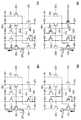
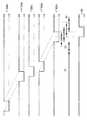
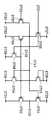
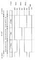
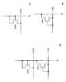
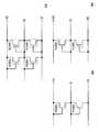
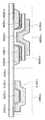
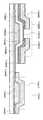
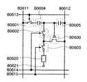
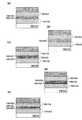
상기에서 나타낸 내부회로 중에서도, 비결정 반도체로 구성된 트랜지스터(이하, 아모퍼스 실리콘 트랜지스터라고도 한다)을 사용한 시프트 레지스터가 고안되어 있다. 종래의 시프트 레지스터가 가지는 플립플롭의 구성을 도100a에 나타낸다(특허문헌 1). 도100a의 플립플롭은, 트랜지스터 11(부트스트랩용 트랜지스터), 트랜지스터 12, 트랜지스터 13, 트랜지스터 14, 트랜지스터 15, 트랜지스터 16 및 트랜지스터 17을 가지고, 신호선 21, 신호선 22, 배선 23, 신호선 24, 전원선 25, 전원선 26에 접속되어 있다. 신호선 21, 신호선 22, 신호선 24, 전원선 25, 전원선 26에는, 각각 스타트 신호, 리셋트 신호, 클록 신호, 전원 전위 VDD, 전원전위 VSS가 입력된다. 도100a의 플립플롭의 동작 기간은, 도100b의 타이밍 차트에 도시된 것과 같이 세트 기간, 선택 기간, 리셋트 기간, 비선택 기간으로 분할된다.Among the internal circuits shown above, a shift register using a transistor composed of an amorphous semiconductor (hereinafter also referred to as an amorphous silicon transistor) has been devised. The structure of the flip-flop which a conventional shift register has is shown by FIG. 100A (patent document 1). The flip-flop of Fig. 100A has a transistor 11 (bootstrap transistor), a
세트 기간에 있어서, 신호선 21로부터 H신호를 입력하고, 노드 41의 전위를 VDD-Vth15(Vth15: 트랜지스터 15의 임계전압)로 상승시킴으로써 트랜지스터 11을 온한 채 노드 41을 부유 상태로 하고 있다. 트랜지스터 16은, 신호선 21로부터 H신호가 입력될 때에는 온되어 있으므로, 노드 41에 게이트 전극이 접속된 트랜지스터 14가 온되어, 노드 42의 전위를 L레벨로 함으로써 트랜지스터 16을 오프하고 있다. 즉, 신호선 21에 H신호가 입력되고나서, 트랜지스터 16이 오프할 때까지의 기간은, 트랜지스터 11의 게이트 전극에서 전하가 새고 있었다.In the set period, the H signal is input from the
여기에서, 전위가 VDD인 신호를 H신호, 전위가 VSS인 신호를 L신호라고 부른다. 또한 L레벨이란, L신호의 전위가 VSS인 것을 말한다.Here, a signal having a potential of VDD is called an H signal, and a signal having a potential of VSS is called an L signal. The L level means that the potential of the L signal is VSS.
비특허문헌1 및 비특허문헌2의 표시장치는, 아모퍼스 실리콘 트랜지스터로 구성되는 시프트 레지스터를 주사선구동회로로서 사용하고, 다시 R, G, B의 서브 화소에 1개의 신호선에서 비디오신호를 입력함으로써 신호선의 수를 1/3로 줄이고 있다. 이렇게 해서, 비특허문헌1 및 비특허문헌2의 표시장치는, 표시 패널과 드라이버 IC의 접속수를 절감하고 있다.The display devices of Non-Patent
[특허문헌1] 일본국 특개2004-157508호 공보[Patent Document 1] Japanese Patent Application Laid-Open No. 2004-157508
[비특허문헌1] Jin Young Choi, et al. "A Compact and Cost-ef ficient TFT-LCD through the Triple-Gate Pixel Structure", SOCIETY FOR INFORMATION DISPLAY 2006 INTERNATIONAL SYMPOSIUM DIGEST OF TECHNICAL PAPERS, Volume XXXVII, p.274-276[Non-Patent Document 1] Jin Young Choi, et al. "A Compact and Cost-efficient TFT-LCD through the Triple-Gate Pixel Structure", SOCIETY FOR INFORMATION DISPLAY 2006 INTERNATIONAL SYMPOSIUM DIGEST OF TECHNICAL PAPERS, Volume XXXVII, p.274-276
[비특허문헌2] Yong Soon Lee, et al., "Advanced TFT-LCD Data Line Reduction Method", SOCIETY FOR INFORMATION DISPLAY 2006 INTERNATIONAL SYMPOSIUM DIGEST OF TECHNICAL PAPERS, Volume XXXVII, p. 1083-1086
[Non-Patent Document 2] Yong Soon Lee, et al., "Advanced TFT-LCD Data Line Reduction Method", SOCIETY FOR INFORMATION DISPLAY 2006 INTERNATIONAL SYMPOSIUM DIGEST OF TECHNICAL PAPERS, Volume XXXVII, p. 1083-1086
종래의 기술에 의하면, 부트스트랩용 트랜지스터를 온한 채, 부트스트랩용 트랜지스터의 게이트 전극을 부유 상태로 하고 있었다. 그렇지만, 종래의 기술에서는, 부트스트랩용 트랜지스터를 온한 채, 부트스트랩용 트랜지스터의 게이트 전극을 부유 상태로 할 때까지, 시간을 필요로 하기 때문에, 고속으로 동작할 수 없다고 하는 문제가 있었다. 더구나, 트랜지스터의 반도체층으로서 아모퍼스 실리콘을 사용했을 경우, 트랜지스터의 임계전압 시프트를 일으킨다고 하는 문제가 있었다. 더구나, 신호선의 수를 1/3로 줄이고, 표시 패널과 드라이버IC의 접점의 수를 삭감하는 것이 제안되어 있지만(비특허문헌1 및 비특허문헌2), 실용적으로는 드라이버IC의 접점의 수를 한층 더 삭감하는 것이 요구되고 있다.According to the prior art, the gate electrode of the bootstrap transistor is placed in a floating state while the bootstrap transistor is turned on. However, in the related art, since it takes time until the gate electrode of the bootstrap transistor is left in a floating state while the bootstrap transistor is turned on, there is a problem that it cannot operate at high speed. Moreover, when amorphous silicon is used as the semiconductor layer of the transistor, there is a problem that a threshold voltage shift of the transistor occurs. In addition, although it is proposed to reduce the number of signal lines to 1/3 and to reduce the number of contacts between the display panel and the driver IC (
즉, 종래의 기술에서 해결되지 않는 것으로서, 시프트 레지스터가 고속으로 동작할 수 있는 회로 기술, 트랜지스터의 임계전압의 변동을 억제하는 회로 기술이 과제로서 남겨져 있다. 또한 표시 패널에 설치하는 드라이버1C의 접점수를 삭감하는 기술, 표시장치의 저소비 전력화 및 표시장치의 대형화 또는 고선명화도 과제로서 남겨져 있다.That is, as a problem that is not solved in the prior art, a circuit technique in which the shift register can operate at high speed and a circuit technique for suppressing fluctuation of the threshold voltage of the transistor are left as problems. Also, the problem of reducing the number of contacts of the driver 1C installed in the display panel, lowering the power consumption of the display device, and increasing the size or high definition of the display device are left as challenges.
본 명세서의 표시장치는, 부트스트랩용 트랜지스터의 게이트 전극에 접속되는 트랜지스터의 게이트 전극에, 스타트 신호에 의해 제어되는 스위치를 설치하고 있다. 스타트 신호가 입력되면, 스위치를 거쳐 해당 트랜지스터의 게이트 전극에 전위가 공급되어, 해당 트랜지스터는 오프된다. 해당 트랜지스터가 오프되면, 부트스트랩용 트랜지스터의 게이트 전극에서의 전하의 누설을 방지할 수 있다. 따라서, 부트스트랩용 트랜지스터의 게이트 전극에 전하를 충전하기 위한 시간을 빨리 할 수 있으므로, 고속으로 동작할 수 있다.In the display device of the present specification, a switch controlled by a start signal is provided in a gate electrode of a transistor connected to a gate electrode of a bootstrap transistor. When the start signal is input, the potential is supplied to the gate electrode of the transistor via a switch, and the transistor is turned off. When the transistor is turned off, leakage of charge at the gate electrode of the bootstrap transistor can be prevented. Therefore, the time for charging the gate electrode of the bootstrap transistor can be increased quickly, and the operation can be performed at high speed.
본 서류(명세서, 특허청구범위 또는 도면 등)에 나타내는 스위치는, 여러가지 형태의 것을 사용할 수 있다. 예로서는, 전기적 스위치나 기계적 스위치 등이 있다. 즉, 전류의 흐름을 제어할 수 있는 것이면 되고, 특정한 것에 한정되지 않는다. 예를 들면 스위치로서, 트랜지스터(예를 들면 바이폴러트랜지스터, MOS 트랜지스터 등), 다이오드(예를 들면 PN다이오드, PIN다이오드, 쇼트키 다이오드, MIM(Metal Insulator Metal)다이오드, MIS(Metal Insulator Semiconductor)다이오드, 다이오드 접속의 트랜지스터 등), 사이리스터등을 사용할 수 있다. 또한 이것들을 조합한 논리회로를 스위치로서 사용할 수 있다.The switch shown in this document (specifications, claims, drawings, etc.) can use various forms. Examples include electrical switches and mechanical switches. That is, it is only required to be able to control the flow of the current, and the present invention is not limited to a specific one. For example, as a switch, a transistor (for example, a bipolar transistor, a MOS transistor, etc.), a diode (for example, a PN diode, a PIN diode, a Schottky diode, a metal insulator metal (MIM) diode, a metal insulator semiconductor (MIS) diode) , Transistors of diode connection, etc.), thyristors, etc. can be used. Moreover, the logic circuit which combined these can be used as a switch.
스위치로서 트랜지스터를 사용할 경우, 그 트랜지스터는, 단순한 스위치로서 동작하기 때문에, 트랜지스터의 극성(도전형)은 특별하게 한정되지 않는다. 다만, 오프 전류를 억제하고 싶을 경우, 오프 전류가 적은 쪽의 극성의 트랜지스터를 사용하는 것이 바람직하다. 오프 전류가 적은 트랜지스터로서는, LDD 영역을 가지는 트랜지스터나 멀티 게이트 구조를 가지는 트랜지스터 등이 있다. 또한 스위치로서 동작시키는 트랜지스터의 소스 단자의 전위가, 저전위측 전원(Vss, GND, 0V 등)에 가까운 상태에서 동작하는 경우에는, N채널형 트랜지스터를 사용하는 것이 바람직하다. 반대로, 소스 단자의 전위가, 고전위측 전원(Vdd 등)에 가까운 상태에서 동작하는 경우에는, P채널형 트랜지스터를 사용하는 것이 바람직하다. 왜냐하면, N채널형 트랜지스터의 소스 단자가 저전위측 전원에 가까운 상태에서 동작할 때, 또는 P채널형 트랜지스터의 소스 단자가 고전위측 전원에 가까운 상태에서 동작할 때에는, 게이트?소스간 전압의 절대값을 크게 할 수 있어, 스위치의 온 또는 오프의 전환이 용이하게 되기 때문이다. 또한 트랜지스터가 소스 폴로워 동작을 해 버리는 일이 적기 때문에, 출력 전압의 크기가 작아져 버리는 일이 적기 때문이다.When a transistor is used as the switch, since the transistor operates as a simple switch, the polarity (conductive type) of the transistor is not particularly limited. However, when it is desired to suppress the off current, it is preferable to use a transistor having a polarity with a smaller off current. As a transistor with few off currents, there are a transistor having an LDD region, a transistor having a multi-gate structure, and the like. In the case where the potential of the source terminal of the transistor to be operated as a switch is close to the low potential power source (Vss, GND, 0V, etc.), it is preferable to use an N-channel transistor. In contrast, when the potential of the source terminal operates in a state close to a high potential power supply (Vdd or the like), it is preferable to use a P-channel transistor. This is because when the source terminal of the N-channel transistor operates near the low potential power supply, or when the source terminal of the P channel transistor operates near the high potential power supply, the absolute value of the gate-source voltage is achieved. This is because the size of the switch can be increased, and switching of the switch on or off becomes easy. In addition, since the transistor is less likely to perform the source follower operation, the magnitude of the output voltage is less likely to be reduced.
N채널형 트랜지스터와 P채널형 트랜지스터의 양쪽을 사용하여, CMOS형 스위치를 스위치로서 사용해도 된다. CMOS형 스위치로 하면, P채널형 트랜지스터 또는 N채널형 트랜지스터의, 어느 한쪽의 트랜지스터가 도통하면 전류가 흐르기 때문에, 스위치로서 기능하기 쉬워진다. 예를 들면 스위치에의 입력 신호의 전압이 높은 경우에도, 낮은 경우에도, 적절하게 전압을 출력시킬 수 있다. 더구나, 스위치를 온?오프시키기 위한 신호의 전압 진폭값을 작게 할 수 있으므로, 소비 전력을 작게 할 수도 있다.Both the N-channel transistor and the P-channel transistor may be used to use a CMOS switch as a switch. When a CMOS switch is used, current flows when either transistor of the P-channel transistor or the N-channel transistor is turned on, so that it becomes easy to function as a switch. For example, even when the voltage of the input signal to the switch is high or low, the voltage can be appropriately output. Moreover, since the voltage amplitude value of the signal for turning the switch on and off can be made small, the power consumption can be made small.
스위치로서 트랜지스터를 사용할 경우, 스위치는, 입력 단자(소스 단자 및 드레인 단자의 한쪽)와, 출력 단자(소스 단자 및 드레인 단자의 다른 쪽)과, 도통을 제어하는 단자(게이트 단자)를 가지고 있다. 한편, 스위치로서 다이오드를 사용할 경우, 스위치는, 도통을 제어하는 단자를 가지지 않고 있을 경우가 있다. 그 때문에 트랜지스터보다도 다이오드를 스위치로서 사용하는 쪽이, 단자를 제어하기 위한 배선을 적게 할 수 있다.When a transistor is used as the switch, the switch has an input terminal (one of the source terminal and the drain terminal), an output terminal (the other of the source terminal and the drain terminal), and a terminal (gate terminal) for controlling conduction. On the other hand, when using a diode as a switch, the switch may not have the terminal which controls conduction. Therefore, the use of a diode as a switch rather than a transistor can reduce the wiring for controlling the terminal.
본 명세서에 있어서, A와 B가 접속되어 있다고 명시적으로 기재하는 경우에는, A와 B가 전기적으로 접속되어 있을 경우와, A와 B가 기능적으로 접속되어 있을 경우와, A와 B가 직접 접속되어 있을 경우를 포함하는 것으로 한다. 여기에서, A, B는, 대상물(예를 들면 장치, 소자, 회로, 배선, 전극, 단자, 도전막, 층 등)인 것으로 한다. 따라서, 본 명세서가 개시하는 구성에 있어서, 소정의 접속 관계, 예를 들면 도면 또는 문장에 표시된 접속 관계에 한정되지 않고, 도면 또는 문장에 표시된 접속 관계 이외의 것도 포함하는 것으로 한다.In the present specification, when explicitly describing that A and B are connected, when A and B are electrically connected, when A and B are functionally connected, and A and B are directly connected It shall be included when there is. Here, A and B shall be an object (for example, an apparatus, an element, a circuit, wiring, an electrode, a terminal, a conductive film, a layer, etc.). Therefore, in the structure disclosed by this specification, it is not limited to the predetermined connection relationship, for example, the connection relationship shown in a figure or a sentence, and shall also include other than the connection relationship shown in a figure or a sentence.
예를 들면 A와 B가 전기적으로 접속되어 있을 경우로서, A와 B의 전기적인 접속을 가능하게 하는 소자(예를 들면 스위치, 트랜지스터, 용량소자, 인덕터, 저항소자, 다이오드 등)가, A와 B의 사이에 1개 이상 배치되어 있어도 된다. 또는, A와 B가 기능적으로 접속되어 있을 경우로서, A와 B의 기능적인 접속을 가능하게 하는 회로(예를 들면 논리회로(인버터, NAND회로, NOR회로 등), 신호변환회로(DA변환 회로, AD변환 회로, 감마 보정회로 등), 전위 레벨 변환 회로(전원회로(승압회로, 강압회로 등), 신호의 전위 레벨을 바꾸는 레벨 시프터 회로 등), 전압원, 전류원, 변환 회로, 증폭회로(신호 진폭 또는 전류량 등을 크게 할 수 있는 회로, OP앰프, 차동증폭회로, 소스 폴로워 회로, 버퍼 회로 등), 신호 생성 회로, 기억 회로, 제어회로 등)이, A와 B의 사이에 1개 이상 배치되어 있어도 된다. 또는, A와 B가 직접 접속되어 있을 경우로서, A와 B의 사이에 다른 소자나 다른 회로를 끼우지 않고, A와 B가 직접 접속되어 있어도 된다.For example, in the case where A and B are electrically connected, an element (for example, a switch, a transistor, a capacitor, an inductor, a resistor, a diode, etc.) that enables the electrical connection between A and B is A and B. One or more may be arrange | positioned between B. Alternatively, when A and B are functionally connected, a circuit (for example, a logic circuit (inverter, NAND circuit, NOR circuit, etc.) that enables functional connection of A and B), a signal conversion circuit (DA conversion circuit) , AD conversion circuit, gamma correction circuit, etc.), potential level conversion circuit (power supply circuit (step-up circuit, step-down circuit, etc.), level shifter circuit for changing the potential level of the signal), voltage source, current source, conversion circuit, amplification circuit (signal) One or more circuits (op amps, differential amplifier circuits, source follower circuits, buffer circuits, etc.), signal generation circuits, memory circuits, control circuits, etc.) capable of increasing the amplitude or the amount of current, etc. It may be arranged. Or when A and B are directly connected, A and B may be directly connected, without inserting another element or another circuit between A and B. FIG.
A와 B가 직접 접속되어 있다고 명시적으로 기재하는 경우에는, A와 B가 직접 접속되어 있는 경우(즉, A와 B의 사이에 다른 소자나 다른 회로를 사이에 개재하지 않고 접속되어 있을 경우)와, A와 B가 전기적으로 접속되어 있을 경우(즉, A와 B의 사이에 별도의 소자나 별도의 회로를 끼워서 접속되어 있을 경우)를 포함하는 것으로 한다.When explicitly stating that A and B are directly connected, when A and B are directly connected (that is, when A and B are connected without interposing another element or another circuit between them). And the case where A and B are electrically connected (that is, when a separate element or a separate circuit is inserted between A and B).
A와 B가 전기적으로 접속되어 있다고 명시적으로 기재하는 경우에는, A와 B가 전기적으로 접속되어 있을 경우(즉, A와 B의 사이에 별도의 소자나 별도의 회로를 끼워서 접속되어 있을 경우)와, A와 B가 기능적으로 접속되어 있을 경우(즉, A와 B의 사이에 별도의 회로를 끼워서 기능적으로 접속되어 있을 경우)와, A와 B가 직접 접속되어 있을 경우(즉, A와 B의 사이에 별도의 소자나 별도의 회로를 끼우지 않고 접속되어 있을 경우)를 포함하는 것으로 한다. 즉, 전기적으로 접속되어 있다고 명시적으로 기재하는 경우에는, 간단히, 접속되어 있다하고만 명시적으로 기재되어 있을 경우와 같은 것으로 한다.When explicitly stating that A and B are electrically connected, when A and B are electrically connected (that is, when a separate element or a separate circuit is inserted between A and B) When A and B are functionally connected (that is, functionally connected by inserting a separate circuit between A and B), and when A and B are directly connected (that is, A and B In the case of being connected without a separate element or a separate circuit). In other words, when explicitly stated that they are electrically connected, it is assumed that they are simply the same as when explicitly stated only when they are connected.
표시 소자, 표시 소자를 가지는 장치인 표시장치, 발광소자, 발광소자를 가지는 장치인 발광 장치는, 여러가지의 형태에 사용할 수 있고, 또한 여러가지의 소자를 가질 수 있다. 예를 들면 표시 소자, 표시장치, 발광소자 또는 발광 장치로서는, EL소자(유기 EL소자, 무기 EL소자 또는 유기물 및 무기물을 포함하는 EL소자), 전자방출소자, 액정소자, 전자 잉크, 전기영동소자, 그레이팅 라이트밸브(GLV), 플라즈마 디스플레이(PDP), 디지털 마이크로미러 디바이스(DMD), 압전 세라믹 디스플레이, 카본 나노튜브 등, 전기자기적 작용에 의해, 콘트라스트, 휘도, 반사율, 투과율 등이 변화되는 표시 매체를 사용할 수 있다. 이때, EL소자를 사용한 표시장치로서는 EL디스플레이, 전자방출소자를 사용한 표시장치로서는 필드 에미션 디스플레이(FED)나 SED 방식 평면형 디스플레이(SED: Surface-Conduction Electron-emitter Display) 등, 액정소자를 사용한 표시장치로서는 액정 디스플레이(투과형 액정 디스플레이, 반투과형 액정 디스플레이, 반사형 액정 디스플레이, 직시형 액정 디스플레이, 투사형 액정 디스플레이), 전자 잉크나 전기영동소자를 사용한 표시장치로서는 전자 페이퍼가 있다.The display element, the display device which is a device which has a display element, the light emitting element, and the light emitting device which is a device which has a light emitting element can be used for various forms, and can also have various elements. For example, as a display element, a display device, a light emitting element or a light emitting device, an EL element (organic EL element, an inorganic EL element or an EL element containing an organic substance and an inorganic substance), an electron emitting element, a liquid crystal element, an electronic ink, an electrophoretic element Display medium whose contrast, brightness, reflectance, transmittance, etc. are changed by electromagnetism such as grating light valve (GLV), plasma display (PDP), digital micromirror device (DMD), piezoelectric ceramic display, carbon nanotube, etc. Can be used. In this case, an EL display is used as a display device using an EL element, and a display is used using a liquid crystal device such as a field emission display (FED) or a SED type flat panel display (SED) as a display device using an electron emitting device. Examples of the device include liquid crystal displays (transmissive liquid crystal displays, transflective liquid crystal displays, reflective liquid crystal displays, direct-view liquid crystal displays, projection liquid crystal displays), and electronic paper as display devices using electronic ink or electrophoretic elements.
본 서류(명세서, 특허청구범위 또는 도면 등)에 기재된 트랜지스터로서, 여러가지 형태의 트랜지스터를 사용할 수 있다. 따라서, 사용하는 트랜지스터의 종류에 한정은 없다. 예를 들면 비정질 실리콘, 다결정 실리콘, 미결정(마이크로 크리스탈, 세미아모퍼스라고도 한다) 실리콘 등으로 대표되는 비단결정 반도체막을 가지는 박막트랜지스터(TFT) 등을 사용할 수 있다. TFT를 사용할 경우, 여러가지의 장점이 있다. 예를 들면 단결정 실리콘의 경우보다도 낮은 온도에서 제조할 수 있기 때문에, 제조 비용의 삭감, 또는 제조 장치의 대형화를 꾀할 수 있다. 제조 장치의 대형화에 의해, 대형기판 위에 트랜지스터를 제조할 수 있다. 그 결과, 저비용으로, 동시에 많은 개수의 표시장치를 제조할 수 있다. 더구나, 제조 온도가 낮기 때문에, 내열성이 약한 기판을 사용할 수 있다. 그 때문에 투명기판 위에 트랜지스터를 제조할 수 있다. 그 결과, 투명기판 상의 트랜지스터를 사용하여, 표시 소자에서의 빛의 투과를 제어할 수 있다. 또는, 트랜지스터의 막두께가 얇기 때문에, 트랜지스터를 구성하는 막의 일부는, 빛을 투과시킬 수 있다. 그 결과, 개구율을 향상시킬 수 있다.As the transistor described in this document (specifications, claims, drawings, etc.), various types of transistors can be used. Therefore, there is no limitation in the kind of transistor to be used. For example, a thin film transistor (TFT) having a non-single-crystal semiconductor film represented by amorphous silicon, polycrystalline silicon, microcrystalline (also called microcrystal, semi-amorphous) silicon, or the like can be used. When using a TFT, there are various advantages. For example, since it can manufacture at lower temperature than the case of single crystal silicon, reduction of manufacturing cost or enlargement of a manufacturing apparatus can be aimed at. By increasing the size of the manufacturing apparatus, a transistor can be manufactured on a large substrate. As a result, a large number of display devices can be manufactured at the same time at low cost. Moreover, since a manufacturing temperature is low, the board | substrate with weak heat resistance can be used. Therefore, the transistor can be manufactured on the transparent substrate. As a result, transmission of light in the display element can be controlled by using a transistor on the transparent substrate. Alternatively, since the film thickness of the transistor is thin, part of the film constituting the transistor can transmit light. As a result, the aperture ratio can be improved.
다결정 실리콘을 제조할 때에, 촉매(니켈 등)를 사용함으로써, 결정성을 더욱 더 향상시켜, 전기 특성이 좋은 트랜지스터를 제조하는 것이 가능해진다. 그 결과, 게이트 드라이버 회로(주사선구동회로)이나 소스 드라이버 회로(신호선구동회로), 신호 처리 회로(신호 생성 회로, 감마 보정회로, DA변환 회로 등)을 기판 위에 일체 형성할 수 있다.In producing polycrystalline silicon, by using a catalyst (nickel or the like), it is possible to further improve crystallinity and to manufacture a transistor having good electrical characteristics. As a result, a gate driver circuit (scan line driver circuit), a source driver circuit (signal line driver circuit), and a signal processing circuit (signal generation circuit, gamma correction circuit, DA conversion circuit, etc.) can be integrally formed on the substrate.
미결정 실리콘을 제조할 때에, 촉매(니켈 등)를 사용함으로써, 결정성을 한층 더 향상시켜, 전기 특성이 좋은 트랜지스터를 제조하는 것이 가능해 진다. 이 때, 레이저를 사용하지 않고, 열처리를 가하는 것만으로, 결정성을 향상시킬 수 있다. 그 결과, 게이트 드라이버 회로(주사선구동회로)나 소스 드라이버 회로의 일부(아날로그 스위치 등)를 기판 위에 일체 형성할 수 있다. 더구나, 결정화에 레이저를 사용하지 않는 경우에는, 실리콘의 결정성의 얼룩을 억제할 수 있다. 그 결과, 화질이 향상된 화상을 표시할 수 있다.When producing microcrystalline silicon, by using a catalyst (nickel or the like), it is possible to further improve crystallinity and to manufacture a transistor having good electrical characteristics. At this time, crystallinity can be improved only by applying heat treatment without using a laser. As a result, a part of the gate driver circuit (scanning line driver circuit) or the source driver circuit (analog switch, etc.) can be integrally formed on the substrate. Moreover, in the case where a laser is not used for the crystallization, it is possible to suppress unevenness in crystallinity of the silicon. As a result, an image with improved image quality can be displayed.
단, 촉매(니켈 등)를 사용하지 않고, 다결정 실리콘이나 미결정 실리콘을 제조하는 것은 가능하다.However, it is possible to produce polycrystalline silicon or microcrystalline silicon without using a catalyst (nickel or the like).
반도체기판이나 SOI기판 등을 사용해서 트랜지스터를 형성할 수 있다. 그 경우, MOS형 트랜지스터, 접합형 트랜지스터, 바이폴러트랜지스터 등을 본 명세서에 기재된 트랜지스터로서 사용할 수 있다. 이것들에 의해, 특성이나 사이즈나 형상 등의 격차가 적고, 전류공급 능력이 높고, 사이즈가 작은 트랜지스터를 제조 할 수 있다. 이들 트랜지스터를 사용하면, 회로의 저소비 전력화, 또는 회로의 고집적화를 꾀할 수 있다.The transistor can be formed using a semiconductor substrate, an SOI substrate, or the like. In that case, a MOS transistor, a junction transistor, a bipolar transistor, or the like can be used as the transistor described herein. As a result, a transistor having a small gap in characteristics, size, shape, etc., high current supply capability, and small size can be manufactured. By using these transistors, it is possible to reduce the power consumption of the circuit or to increase the integration of the circuit.
사용할 수 있는 트랜지스터로서, 산화아연(ZnO), 아모퍼스 산화물(a-InGazno), 실리콘 게르마늄(SiGe), 갈륨비소(GaAs), 인듐 아연산화물(IZO), 인듐 주석산화물(ITO), 산화 주석(SnO) 등의 화합물반도체, 또는 산화물반도체를 가지는 트랜지스터나, 더구나, 이것들의 화합물반도체 또는 산화물반도체를 박막화한 박막트랜지스터 등이 있다. 이것들에 의해, 제조 온도를 낮게 할 수 있고, 예를 들면 실온에서 트랜지스터를 제조하는 것이 가능해 진다. 그 결과, 내열성이 낮은 기판, 예를 들면 플라스틱 기판이나 필름 기판에 직접 트랜지스터를 형성할 수 있다. 또한, 이것들의 화합물반도체 또는 산화물반도체를, 트랜지스터의 채널 부분에 사용할 뿐만 아니라, 그 이외의 용도로 사용할 수도 있다. 예를 들면 이러한 화합물반도체 또는 산화물반도체를 저항소자, 화소전극, 투명전극으로서 사용할 수 있다. 더구나, 그것들을 트랜지스터와 동시에 성막 또는 형성할 수 있기 때문에, 비용을 저감할 수 있다.As a transistor that can be used, zinc oxide (ZnO), amorphous oxide (a-InGazno), silicon germanium (SiGe), gallium arsenide (GaAs), indium zinc oxide (IZO), indium tin oxide (ITO), tin oxide ( And a transistor having a compound semiconductor such as SnO) or an oxide semiconductor, and a thin film transistor obtained by thinning these compound semiconductors or oxide semiconductors. By these, a manufacturing temperature can be made low and it becomes possible to manufacture a transistor at room temperature, for example. As a result, the transistor can be formed directly on a substrate having low heat resistance, for example, a plastic substrate or a film substrate. These compound semiconductors or oxide semiconductors can be used not only for the channel portion of the transistor but also for other uses. For example, such a compound semiconductor or an oxide semiconductor can be used as a resistance element, a pixel electrode, or a transparent electrode. Moreover, since they can be formed or formed simultaneously with the transistor, the cost can be reduced.
사용할 수 있는 트랜지스터로서, 잉크젯이나 인쇄법을 사용해서 형성한 트랜지스터 등이 있다. 이것들에 의해, 트랜지스터를 실온에서 제조, 저진공도에서 제조, 또는 대형기판 위에 제조 할 수 있다. 또한 마스크(레티클)를 사용하지 않아도 제조하는 것이 가능해지기 때문에, 트랜지스터의 배치를 용이하게 변경할 수 있다. 더구나, 레지스트를 사용할 필요가 없기 때문에, 재료비가 싸고, 공정수를 삭감할 수 있다. 더구나, 필요한 부분에만 막을 붙이기 때문에, 전체면에 성막한 후에 에칭한고 하는 제조방법보다도, 재료가 쓸데 없어지지 않아, 저비용으로 할 수 있다.As a transistor which can be used, the transistor formed using the inkjet and the printing method, etc. are mentioned. These can produce the transistor at room temperature, at low vacuum, or on a large substrate. In addition, since manufacturing can be performed without using a mask (reticle), the arrangement of transistors can be easily changed. Moreover, since there is no need to use a resist, the material cost is low and the number of steps can be reduced. In addition, since the film is applied only to the required portion, the material is not wasteful and can be made at a lower cost than the manufacturing method of etching after film formation on the entire surface.
사용할 수 있는 트랜지스터로서, 유기반도체나 카본 나노튜브를 가지는 트랜지스터 등이 있다. 이것들에 의해, 구부리는 것이 가능한 기판 위에 트랜지스터를 형성할 수 있다. 그 때문에 유기반도체나 카본 나노튜브를 가지는 트랜지스터 등을 사용한 장치는, 충격에 강하게 할 수 있다.Examples of the transistor that can be used include an organic semiconductor and a transistor having carbon nanotubes. These can form a transistor on the substrate which can be bent. Therefore, the apparatus using the transistor etc. which have an organic semiconductor, a carbon nanotube, can be made strong in an impact.
기타, 여러가지의 트랜지스터를 사용할 수 있다.In addition, various transistors can be used.
트랜지스터가 형성되어 있는 기판의 종류는, 여러가지의 것을 사용할 수 있고, 특정한 것에 한정될 일은 없다. 트랜지스터가 형성되는 기판으로서는, 예를 들면 단결정 기판, SOI기판, 유리 기판, 석영기판, 플라스틱 기판, 종이기판, 셀로판 기판, 석재기판, 목재기판, 천기판(천연섬유(견, 면, 마), 합성 섬유(나이론, 폴리우레탄, 폴리에스테르) 혹은 재생 섬유(아세테이트, 큐프라, 레이온, 재생 폴리에스테르) 등을 포함한다), 피혁기판, 고무 기판, 스테인레스?스틸 기판, 스테인레스?스틸?호일을 가지는 기판 등을 사용할 수 있다. 또는, 사람 등의 동물의 피부(피부 표면, 진피) 또는 피하조직을 기판으로서 사용해도 된다. 또는, 어떤 기판으로 트랜지스터를 형성하고, 그 후에 별도의 기판에 트랜지스터를 전치해도 좋다. 트랜지스터가 전치되는 기판으로서는, 단결정 기판, SOI기판, 유리 기판, 석영기판, 플라스틱 기판, 종이기판, 셀로판 기판, 석재기판, 목재기판, 천기판(천연섬유(견, 면, 마), 합성 섬유(나이론, 폴리우레탄, 폴리에스테르) 혹은 재생 섬유(아세테이트, 큐프라, 레이온, 재생 폴리에스테르) 등을 포함한다), 피혁기판, 고무 기판, 스테인레스?스틸 기판, 스테인레스?스틸?호일을 가지는 기판 등을 사용할 수 있다. 또는, 사람등 의 동물의 피부(피부 표면, 진피) 또는 피하조직을 트랜지스터가 전치되는 기판으로서 사용해도 된다. 이들 기판을 사용함으로써, 특성이 좋은 트랜지스터의 형성, 소비 전력이 작은 트랜지스터의 형성, 깨지기 어려운 장치의 제조, 내열성의 부여, 또는 경량화를 꾀할 수 있다.Various kinds of substrates in which a transistor is formed can be used, and are not limited to a specific one. Examples of the substrate on which the transistor is formed include, for example, a single crystal substrate, an SOI substrate, a glass substrate, a quartz substrate, a plastic substrate, a paper substrate, a cellophane substrate, a stone substrate, a wood substrate, and a substrate (natural fibers (dog, cotton, hemp), Synthetic fibers (including nylon, polyurethane, polyester) or recycled fibers (including acetate, cupra, rayon, recycled polyester), leather substrates, rubber substrates, stainless steel substrates, stainless steel foils Substrates and the like can be used. Alternatively, the skin (skin surface, dermis) or subcutaneous tissue of an animal such as a human may be used as the substrate. Alternatively, the transistor may be formed of a substrate, and then the transistor may be transferred to another substrate. Substrates to which transistors are transposed include single crystal substrates, SOI substrates, glass substrates, quartz substrates, plastic substrates, paper substrates, cellophane substrates, stone substrates, wood substrates, perforated substrates (natural fibers (dog, cotton, hemp), synthetic fibers ( Nylon, polyurethane, polyester) or regenerated fibers (including acetate, cupra, rayon, regenerated polyester), leather substrates, rubber substrates, stainless steel substrates, stainless steel foil substrates, and the like. Can be used. Alternatively, the skin (skin surface, dermis) or subcutaneous tissue of an animal such as a human may be used as the substrate on which the transistor is placed. By using these substrates, it is possible to form a transistor having good characteristics, to form a transistor having low power consumption, to manufacture a fragile device, to impart heat resistance, or to reduce weight.
트랜지스터의 구성은, 여러가지의 형태를 취할 수 있고, 특정한 구성에 한정되지 않는다. 예를 들면 게이트 전극이 2개 이상인 멀티 게이트 구조를 사용해도 된다. 멀티 게이트 구조로 하면, 채널 영역이 직렬로 접속되기 때문에, 복수의 트랜지스터가 직렬로 접속된 구성이 된다. 멀티 게이트 구조에 의해, 오프 전류의 저감, 트랜지스터의 내압향상에 의한 신뢰성의 향상을 꾀할 수 있다. 또는, 멀티 게이트 구조에 의해, 포화 영역에서 동작할 때에, 드레인?소스간 전압이 변화되어도, 드레인?소스간 전류가 그다지 변화되지 않아, 기울기가 플랫한 전압?전류특성을 얻을 수 있다. 기울기가 플랫한 전압?전류특성을 이용하면, 이상적인 전류원 회로나, 대단히 높은 저항치를 가지는 능동부하를 실현할 수 있다. 그 결과, 특성이 좋은 차동 회로나 커런트미러회로를 실현할 수 있다. 또한 채널의 상하에 게이트 전극이 배치되어 있는 구조이어도 된다. 채널의 상하에 게이트 전극이 배치되어 있는 구조로 하는 것에 의해, 채널 영역이 증가하기 때문에, 전류치의 증가, 또는 공핍층이 생기기 쉬워지는 것에 의한 S값의 저감을 꾀할 수 있다. 채널의 상하에 게이트 전극이 배치되면, 복수의 트랜지스터가 병렬로 접속된 구성이 된다.The configuration of the transistor can take various forms and is not limited to a specific configuration. For example, a multi-gate structure having two or more gate electrodes may be used. In the multi-gate structure, since the channel regions are connected in series, a plurality of transistors are connected in series. By the multi-gate structure, it is possible to reduce the off current and improve the reliability by improving the breakdown voltage of the transistor. Alternatively, when the multi-gate structure operates in the saturation region, even if the drain-source voltage changes, the drain-source current does not change very much, so that the voltage and current characteristics with a flat slope can be obtained. By using a voltage and current characteristic with a flat slope, an ideal current source circuit and an active load having a very high resistance value can be realized. As a result, a differential circuit and a current mirror circuit with good characteristics can be realized. In addition, the structure in which the gate electrode is arrange | positioned above and below a channel may be sufficient. By having the structure in which the gate electrodes are arranged above and below the channel, the channel region is increased, so that the S value can be reduced by increasing the current value or easily forming a depletion layer. When the gate electrodes are arranged above and below the channel, a plurality of transistors are connected in parallel.
기타, 채널 영역 위에 게이트 전극이 배치되어 있는 구조라도 되고, 채널 영역 밑에 게이트 전극이 배치되어 있는 구조이어도 된다. 또는, 정 스태거 구조 또는 역 스태거 구조하도 되고, 채널 영역이 복수개 영역으로 나뉘어져 있어도 되고, 채널 영역이 병렬로 접속되어 있어도 되고, 채널 영역이 직렬로 접속되어 있어도 된다. 또한 채널 영역(혹은 그 일부)에 소스 전극이나 드레인 전극이 겹쳐서 있어도 된다. 채널 영역(혹은 그 일부)에 소스 전극이나 드레인 전극이 겹치는 구조로 하는 것에 의해, 채널 영역의 일부에 전하가 모여, 동작이 불안정해지는 것을 막을 수 있다. 또한 LDD영역을 형성해도 된다. LDD 영역을 설치함으로써, 오프 전류의 저감, 또는 트랜지스터의 내압향상에 의한 신뢰성의 향상을 꾀할 수 있다. 또는, LDD 영역을 설치함으로써, 포화 영역에서 동작할 때에, 드레인?소스간 전압이 변화되어도, 드레인?소스간 전류가 그다지 변화되지 않아, 전압?전류특성의 기울기가 플랫한 특성으로 할 수 있다.In addition, the structure in which the gate electrode is arrange | positioned on a channel area may be sufficient, and the structure in which the gate electrode is arrange | positioned under a channel area may be sufficient. Alternatively, the normal staggered structure or the reverse staggered structure may be provided, the channel region may be divided into a plurality of regions, the channel regions may be connected in parallel, or the channel regions may be connected in series. In addition, the source electrode and the drain electrode may overlap the channel region (or part thereof). The structure in which the source electrode and the drain electrode overlap with the channel region (or part thereof) can prevent charges from gathering in a part of the channel region, thereby preventing the operation from becoming unstable. In addition, an LDD region may be formed. By providing the LDD region, it is possible to reduce the off current or to improve the reliability by improving the breakdown voltage of the transistor. Alternatively, by providing the LDD region, even when the drain-source voltage changes when operating in the saturation region, the drain-source current does not change very much, so that the slope of the voltage-current characteristic can be flat.
본 명세서에 있어서의 트랜지스터는, 여러가지의 타입을 사용할 수 있고, 여러가지의 기판 위에 형성할 수 있다. 따라서, 소정의 기능을 실현하기 위해서 필요한 회로의 모두가, 동일기판 위에 형성되어 있어도 된다. 예를 들면 소정의 기능을 실현하기 위해서 필요한 회로의 모두가, 유리 기판상, 플라스틱 기판상, 단결정 기판상, 또는 SOI 기판 위에 형성되어 있어도 되고, 그 외 여러가지의 기판 위에 형성되어 있어도 된다. 소정의 기능을 실현하기 위해서 필요한 회로의 모두가, 같은 기판 위에 형성되어 있는 것에 의해, 부품수를 줄여 비용을 저감하고, 회로부품과의 접속 점수를 절감해서 신뢰성을 향상시킬 수 있다. 또는, 소정의 기능을 실현하기 위해서 필요한 회로의 일부가, 어떤 기판 위에 형성되고 있고, 소정의 기능을 실현시키기 위해서 필요한 회로의 다른 일부가, 별도의 기판 위에 형성되어 있어도 된다. 즉, 소정의 기능을 실현하기 위해서 필요한 회로의 모두가, 같은 기판 위에 형성되지 않고 있어도 좋다. 예를 들면 소정의 기능을 실현하기 위해서 필요한 회로의 일부는, 유리 기판 위에 트랜지스터를 사용해서 형성되고, 소정의 기능을 실현하기 위해서 필요한 회로의 다른 일부는, 단결정 기판 위에 형성되어, 단결정 기판상의 트랜지스터에서 구성된 IC칩을, COG(Chip On Glass)로 유리 기판에 접속하고, 유리 기판 위에 그 IC칩을 배치해도 좋다. 또는, 그 IC칩을 TAB(Tape Automated Bonding)이나 프린트 기판을 사용해서 유리 기판과 접속해도 좋다. 이렇게, 회로의 일부가 같은 기판 위에 형성되어 있는 것에 의해, 부품수를 줄여서 비용을 저감하고, 회로부품과의 접속 점수를 절감해서 신뢰성을 향상시킬 수 있다. 또한 구동전압이 높은 부분이나 구동주파수가 높은 부분의 회로는, 소비 전력이 커져버리므로, 그러한 부분의 회로는 같은 기판 위에 형성하지 않고, 그 대신에, 단결정 기판 위에 그 부분의 회로를 형성하고, 그 회로로 구성된 IC칩을 사용하도록 하면, 소비 전력의 증가를 막을 수 있다.The transistor in this specification can use various types, and can form it on various board | substrates. Therefore, all of the circuits necessary for realizing a predetermined function may be formed on the same substrate. For example, all of the circuits necessary for realizing a predetermined function may be formed on a glass substrate, a plastic substrate, a single crystal substrate, or an SOI substrate, or may be formed on various other substrates. Since all the circuits necessary for realizing a predetermined function are formed on the same substrate, the number of parts can be reduced, the cost can be reduced, the connection point with the circuit parts can be reduced, and the reliability can be improved. Alternatively, a part of the circuit necessary for realizing the predetermined function may be formed on a certain substrate, and another part of the circuit necessary for realizing the predetermined function may be formed on another substrate. That is, all of the circuits necessary for realizing a predetermined function may not be formed on the same substrate. For example, a part of a circuit necessary for realizing a predetermined function is formed using a transistor on a glass substrate, and another part of a circuit required for realizing a predetermined function is formed on a single crystal substrate, and the transistor on a single crystal substrate is The IC chip constructed in the above may be connected to the glass substrate by COG (Chip On Glass), and the IC chip may be disposed on the glass substrate. Alternatively, the IC chip may be connected to a glass substrate using TAB (Tape Automated Bonding) or a printed circuit board. Thus, since a part of a circuit is formed on the same board | substrate, cost can be reduced by reducing the number of components, the connection point with a circuit component can be reduced, and reliability can be improved. In addition, the circuit of a portion having a high driving voltage or a portion having a high driving frequency increases power consumption, so that a circuit of such a portion is not formed on the same substrate. Instead, a circuit of the portion is formed on a single crystal substrate. By using an IC chip composed of the circuit, an increase in power consumption can be prevented.
본 명세서에 있어서는, 1 화소란, 밝기를 제어할 수 있는 요소 1개분을 나타내는 것으로 한다. 일례로서는, 1화소란, 1개의 색요소를 나타내는 것이라고 하고, 그 색요소 1개로 밝기를 표현한다. 따라서, R(빨강) G(초록) B(파랑)의 색요소 이루어지는 컬러 표시장치의 경우에는, 화상의 최소단위는, R의 화소와 G의 화소와 B의 화소의 3화소로 구성되는 것으로 한다. 또한, 색요소는, 3색에 한정되지 않고, 3색 이상을 사용해도 되고, RGB 이외의 색을 사용해도 된다. 예를 들면 W(화이트)을 더해서, RGBW로 해도 된다. 또한 RGB에, 예를 들면 옐로, 시안, 마젠타, 에메럴드 그린, 주색 등을 1색 이상 추가해도 좋다. 또한 예를 들면 RGB 중의 적어도 1색에 유사한 색을, RGB에 추가해도 좋다. 예를 들면 R, G, B1, B2로 해도 된다. B1과 B2는, 어느쪽도 청색이지만, 약간 주파수가 다르다. 마찬가지로, R1, R2, G, B로 해도 된다. 이러한 색요소를 사용함으로써, 보다 실물에 가깝게 표 할 수 있고, 또한 소비 전력을 저감할 수 있다. 다른 예로서는, 1개의 색요소에 대해서, 복수의 영역을 사용해서 밝기를 제어하는 경우에는, 그 영역 1개분을 1 화소로 해도 된다. 일례로서, 면적계조를 행할 경우, 또는 부화소(서브 화소)을 가지고 있을 경우, 1개의 색요소에 따라, 밝기를 제어하는 영역이 복수 있고, 그 전체로 계조를 표현하지만, 그 밝기를 제어하는 영역의 1개분을 1 화소로 해도 된다. 그 경우, 1개의 색요소는, 복수의 화소로 구성된다. 또는, 밝기를 제어하는 영역이 1개의 색요소 중에 복수 있어도, 그것들을 모아, 1개의 색요소를 1 화소로 해도 된다. 그 경우, 1개의 색요소는, 1개의 화소로 구성되게 된다. 또한 1개의 색요소에 대해서, 복수개 영역을 사용해서 밝기를 제어할 경우, 화소에 의해, 표시에 기여하는 영역의 크기가 다른 경우가 있다. 그 경우, 1개의 색요소에 대해서 복수 있는, 밝기를 제어하는 영역에 있어서, 각각에 공급하는 신호를 약간 다르게 하도록 하여, 시야각을 넓혀도 된다. 즉, 1개의 색요소에 대해서, 여러개 있는 영역이 각각 갖는 화소전극의 전위가, 각각 달라도 된다. 그 결과, 액정분자에 가해지는 전압이 각 화소전극에 의해 각각 다르다. 따라서, 시야각을 넓게 할 수 있다.In this specification, 1 pixel shall represent 1 element which can control brightness. As an example, one pixel represents one color element, and the brightness is expressed by one color element. Therefore, in the case of the color display device which consists of the color elements of R (red) G (green) B (blue), the minimum unit of an image shall consist of three pixels of the pixel of R, the pixel of G, and the pixel of B. . In addition, a color element is not limited to 3 colors, 3 or more colors may be used and colors other than RGB may be used. For example, W (white) may be added to make RGBW. In addition, yellow, cyan, magenta, emerald green, cinnabar red, or the like may be added to RGB, for example. For example, a color similar to at least one color of RGB may be added to RGB. For example, it is good also as R, G, B1, and B2. Both B1 and B2 are blue, but slightly different in frequency. Similarly, it is good also as R1, R2, G, B. By using such a color element, it can display more closely to the real thing and can also reduce power consumption. As another example, when brightness is controlled using a plurality of areas for one color element, one area of the area may be one pixel. For example, in case of performing area gradation or having a subpixel (subpixel), there are a plurality of areas for controlling brightness according to one color element, and the gradation is expressed as a whole, but the brightness is controlled. One portion of the region may be one pixel. In that case, one color element is composed of a plurality of pixels. Alternatively, there may be a plurality of regions for controlling the brightness among one color element, or they may be collected and one color element may be one pixel. In that case, one color element is composed of one pixel. In addition, when brightness is controlled using a plurality of areas for one color element, the size of the area contributing to the display may differ depending on the pixel. In this case, it is possible to widen the viewing angle by making a signal to be supplied to each of the plurality of color elements slightly different in the brightness control area. In other words, the potential of the pixel electrode of each of several regions may be different for one color element. As a result, the voltages applied to the liquid crystal molecules are different for each pixel electrode. Therefore, the viewing angle can be widened.
또한, 1 화소(3색분)로 명시적으로 기재하는 경우에는, R와 G과 B의 3화소분을 1 화소로 생각하는 경우이다. 1 화소(1색분)로 명시적으로 기재하는 경우에는, 1개의 색요소에 따라, 복수의 영역이 있을 경우, 그것들을 모아서 1 화소로 생각하는 경우이다.In the case of expressing one pixel (three colors) explicitly, three pixels of R, G, and B are regarded as one pixel. In the case of explicitly describing one pixel (for one color), when there are a plurality of regions according to one color element, it is a case where they are collected and considered as one pixel.
본 서류에 있어서, 화소는, 매트릭스 모양으로 배치(배열)되어 있을 경우가 있다. 여기에서, 화소가 매트릭스로 배치(배열)되어 있다라는 것은, 종방향 혹은 횡방향에 있어서, 화소가 직선 위에 늘어서서 배치되어 있을 경우나, 들쑥날쑥한 선 위에 배치되어 있을 경우를 포함한다. 예를 들면 3색의 색요소(예를 들면 RGB)로 풀컬러 표시할 경우에, 스트라이프 배치되어 있을 경우나, 3개의 색요소의 도트가 델타 배치되어 있을 경우도 포함한다. 더구나, 베이어 배치되어 있을 경우도 포함한다. 또한, 색요소는, 3색에 한정되지 않고, 그 이상이어도 된다. 예를 들면 RGBW(W는 화이트)나, RGB에, 옐로, 시안, 마젠타 등을 1색 이상 추가한 것 등이 있다. 또한 색요소의 도트마다에 그 표시 영역의 크기가 달라도 된다. 이에 따라 저소비 전력화, 또는 표시 소자의 장기 수명화를 꾀할 수 있다.In this document, pixels may be arranged (arranged) in a matrix. Here, the pixels are arranged (arranged) in a matrix, in the case where the pixels are arranged in a line in a longitudinal direction or in a lateral direction, or when they are arranged on a jagged line. For example, when full-color display is performed with three color elements (for example, RGB), the case includes stripe arrangement or the case where dots of three color elements are delta arrangement. Moreover, it also includes the case where a bayer is arrange | positioned. In addition, a color element is not limited to three colors, It may be more than that. For example, RGBW (W is white) and the thing which added one or more colors of yellow, cyan, magenta, etc. to RGB. The size of the display area may be different for each dot of the color element. As a result, low power consumption and long life of the display device can be achieved.
본 서류에 있어서, 화소에 능동소자를 가지는 액티브 매트릭스 방식, 또는, 화소에 능동소자를 가지지 않는 패시브 매트릭스 방식을 사용할 수 있다.In this document, an active matrix method having an active element in a pixel or a passive matrix method having no active element in a pixel can be used.
액티브 매트릭스 방식에서는, 능동소자(액티브 소자, 비선형소자)로서, 트랜지스터 뿐만 아니라, 여러가지의 능동소자(액티브 소자, 비선형소자)를 사용할 수 있다. 예를 들면 MIM(Metal Insulator Metal)이나 TFD(Thin Film Diode) 등을 사용하는 것도 가능하다. 이들 소자는, 제조 공정이 적기 때문에, 제조 비용의 저감, 또는 제품 비율의 향상을 꾀할 수 있다. 더구나, 소자의 사이즈가 작기 때문에, 개구율을 향상시킬 수 있어, 저소비 전력화나 고휘도화를 꾀할 수 있다.In the active matrix system, not only transistors but also various active elements (active elements, nonlinear elements) can be used as active elements (active elements, nonlinear elements). For example, it is also possible to use a metal insulator metal (MIM), a thin film diode (TFD), or the like. Since these elements have few manufacturing processes, reduction of manufacturing cost or improvement of a product ratio can be aimed at. In addition, since the size of the element is small, the aperture ratio can be improved, resulting in low power consumption and high luminance.
액티브 매트릭스 방식 이외의 것으로서, 능동소자(액티브 소자, 비선형소자)를 사용하지 않는 패시브패시브 매트릭스형을 사용하는 것도 가능하다. 능동소자(액티브 소자, 비선형소자)를 사용하지 않기 때문에, 제조 공정이 적고, 제조 비용의 저감, 또는 제품 비율의 향상을 꾀할 수 있다. 또한 능동소자(액티브 소자, 비선형소자)를 사용하지 않기 때문에, 개구율을 향상시킬 수 있어, 저소비 전력화나 고휘도화를 꾀할 수 있다.As other than the active matrix system, it is also possible to use a passive matrix matrix which does not use active elements (active elements, nonlinear elements). Since no active element (active element, nonlinear element) is used, the manufacturing process is small, and the manufacturing cost can be reduced or the product ratio can be improved. In addition, since no active element (active element, nonlinear element) is used, the aperture ratio can be improved, resulting in low power consumption and high luminance.
트랜지스터란, 게이트와, 드레인과, 소스를 포함하는 적어도 3개의 단자를 가지는 소자이며, 드레인 영역과 소스 영역 사이에 채널 영역을 가지고 있어, 드레인 영역과, 채널 영역과, 소스 영역을 거쳐 전류를 흘려보낼 수 있다. 여기에서, 소스와 드레인이란, 트랜지스터의 구조나 동작조건 등에 의해 바뀌기 때문에, 어느 것이 소스 또는 드레인인지를 한정하는 것이 곤란하다. 따라서, 본 명세서에 있어서는, 소스 및 드레인으로서 기능하는 영역을, 소스 혹은 드레인이라고 부르지 않을 경우가 있다. 그 경우, 각각을 제1단자, 제2단자로 표기할 경우가 있다. 또는, 각각을 제1의 전극, 제2의 전극으로 표기할 경우가 있다. 또는, 소스 영역, 드레인 영역으로 표기할 경우가 있다.A transistor is an element having at least three terminals including a gate, a drain, and a source, and has a channel region between the drain region and the source region, and flows current through the drain region, the channel region, and the source region. can send. Here, since the source and the drain change depending on the structure, operation conditions, and the like of the transistor, it is difficult to define which source or drain is the source and the drain. Therefore, in this specification, the area | region which functions as a source and a drain may not be called a source or a drain. In that case, each may be described as a first terminal and a second terminal. Alternatively, each may be referred to as a first electrode or a second electrode. Or it may be described as a source region and a drain region.
트랜지스터는, 베이스와, 에미터와, 콜렉터를 포함하는 적어도 3개의 단자를 가지는 소자이어도 된다. 이 경우도 마찬가지로, 에미터와 콜렉터를, 제1단자, 제2단자로 표기할 경우가 있다.The transistor may be an element having at least three terminals including a base, an emitter, and a collector. In this case as well, the emitter and the collector may be described as the first terminal and the second terminal.
게이트란, 게이트 전극과, 게이트 배선(게이트 선, 게이트 신호선, 주사선, 주사 신호선 등이라고도 한다)을 포함하는 전체, 또는, 그것들의 일부를 말한다. 게이트 전극이란, 채널 영역을 형성하는 반도체와, 게이트 절연막를 거쳐 오버랩하고 있는 부분의 도전막을 말한다. 또한, 게이트 전극의 일부는, LDD(Lightly Doped Drain) 영역, 소스 영역 또는 드레인 영역과, 게이트 절연막를 거쳐 오버랩하고 있을 경우도 있다. 게이트 배선이란, 각 트랜지스터의 게이트 전극의 사이를 접속하기 위한 배선, 각 화소가 가지는 게이트 전극의 사이를 접속하기 위한 배선, 또는 게이트 전극과, 다른 배선을 접속하기 위한 배선을 말한다.The gate means all or part thereof including the gate electrode and the gate wiring (also called a gate line, a gate signal line, a scan line, a scan signal line, and the like). The gate electrode refers to a semiconductor forming the channel region and a conductive film in an overlapping portion via the gate insulating film. A part of the gate electrode may overlap with the lightly doped drain (LDD) region, the source region or the drain region through the gate insulating film. The gate wiring refers to wiring for connecting between the gate electrodes of each transistor, wiring for connecting between the gate electrodes of each pixel, or wiring for connecting the gate electrode and another wiring.
단, 게이트 전극으로서도 기능하고, 게이트 배선으로서도 기능하는 부분(영역, 도전막, 배선 등)도 존재한다. 그러한 부분(영역, 도전막, 배선 등)은, 게이트 전극으로 불러도 되고, 게이트 배선이라고 불러도 된다. 즉, 게이트 전극과 게이트 배선이, 명확하게 구별할 수 없는 영역도 존재한다. 예를 들면 연신해서 배치되어 있는 게이트 배선의 일부와 채널 영역이 오버랩하고 있을 경우, 그 부분(영역, 도전막, 배선 등)은 게이트 배선으로서 기능하고 있지만, 게이트 전극으로소 기능하고 있다. 따라서, 그러한 부분(영역, 도전막, 배선 등)은, 게이트 전극이라고 불러도 되고, 게이트 배선이라고 불러도 된다.However, there are also portions (regions, conductive films, wirings, etc.) which also function as gate electrodes and also as gate wirings. Such portions (regions, conductive films, wirings, etc.) may be referred to as gate electrodes or may be referred to as gate wirings. In other words, there are regions in which the gate electrode and the gate wiring cannot be clearly distinguished. For example, when a portion of the gate wiring extending and the channel region overlap, the portion (region, conductive film, wiring, etc.) functions as a gate wiring, but functions as a gate electrode. Therefore, such a part (region, conductive film, wiring, etc.) may be called a gate electrode, and may be called a gate wiring.
게이트 전극과 같은 재료로 형성되고, 게이트 전극과 같은 섬(아일랜드)을 형성해서 연결되는 부분(영역, 도전막, 배선등)도, 게이트 전극이라고 불러도 된다. 마찬가지로, 게이트 배선과 같은 재료로 형성되고, 게이트 배선과 같은 섬(아일랜드)을 형성해서 연결되는 부분(영역, 도전막, 배선등)도, 게이트 배선이라고 불러도 된다. 이러한 부분(영역, 도전막, 배선 등)은, 엄밀한 의미에서는, 채널 영역과 오버랩하고 있지 않는 경우, 또는 별도의 게이트 전극과 접속시키는 기능을 가지지 않고 있을 경우가 있다. 그러나, 게이트 전극 또는 게이트 배선과 같은 재료로 형성되고, 게이트 전극 또는 게이트 배선과 같은 섬(아일랜드)을 형성해서 연결되는 부분(영역, 도전막, 배선 등)도 있다. 따라서, 그러한 부분(영역, 도전막, 배선 등)도 게이트 전극 또는 게이트 배선이라고 불러도 된다.A portion (region, conductive film, wiring, etc.) formed of the same material as the gate electrode and connected to form an island (island) like the gate electrode may also be referred to as a gate electrode. Similarly, portions (regions, conductive films, wirings, etc.) formed of the same material as the gate wirings and connected to form islands (island) like the gate wirings may also be referred to as gate wirings. Such portions (regions, conductive films, wirings, etc.) are not strictly overlapped with the channel regions or may not have a function of being connected to another gate electrode. However, there is also a portion (region, conductive film, wiring, etc.) formed of the same material as the gate electrode or the gate wiring and connected by forming an island (island) such as the gate electrode or the gate wiring. Therefore, such a part (region, conductive film, wiring, etc.) may also be called a gate electrode or a gate wiring.
예를 들면 멀티 게이트의 트랜지스터에 있어서, 1개의 게이트 전극과, 별도의 게이트 전극과는, 게이트 전극과 같은 재료로 형성된 도전막으로 접속될 경우가 많다. 그러한 부분(영역, 도전막, 배선 등)은, 게이트 전극과, 게이트 전극을 접속시키기 위한 부분(영역, 도전막, 배선 등)이기 때문, 게이트 배선이라고 불러도 되지만, 멀티 게이트의 트랜지스터를 1개의 트랜지스터로 간주할 수도 있기 때문에, 게이트 전극이라고 불러도 된다. 즉, 게이트 전극 또는 게이트 배선과 같은 재료로 형성되고, 게이트 전극 또는 게이트 배선과 같은 섬(아일랜드)을 형성해서 연결되는 부분(영역, 도전막, 배선등)은, 게이트 전극이나 게이트 배선이라고 불러도 된다. 더구나, 게이트 전극과, 게이트 배선을 접속시키고 있는 부분의 도전막으로서, 게이트 전극 또는 게이트 배선과는 다른 재료로 형성된 도전막도, 게이트 전극이라고 불러도 되고, 게이트 배선이라고 불러도 된다.For example, in a multi-gate transistor, one gate electrode and another gate electrode are often connected with a conductive film formed of the same material as the gate electrode. Since such a portion (region, conductive film, wiring, etc.) is a gate electrode and a portion (region, conductive film, wiring, etc.) for connecting the gate electrode, the portion may be referred to as gate wiring. It may be regarded as, so may be called a gate electrode. In other words, a portion (region, conductive film, wiring, etc.) formed of the same material as the gate electrode or the gate wiring and forming an island (island) like the gate electrode or the gate wiring may be called a gate electrode or a gate wiring. . Moreover, as a conductive film of the part which connects a gate electrode and a gate wiring, the conductive film formed from the material different from a gate electrode or a gate wiring may also be called a gate electrode, and may be called a gate wiring.
게이트 단자란, 게이트 전극의 부분(영역, 도전막, 배선 등), 또는 게이트 전극과 전기적으로 접속되어 있는 부분(영역, 도전막, 배선 등)에 대해서, 그 일부분을 말한다.The gate terminal refers to a portion of the gate electrode (region, conductive film, wiring, etc.) or a portion (region, conductive film, wiring, etc.) electrically connected to the gate electrode.
배선을, 게이트 배선, 게이트 선, 게이트 신호선, 주사선, 주사 신호선 등으로 부를 경우, 배선에 트랜지스터의 게이트가 접속되지 않고 있을 경우도 있다. 이 경우, 게이트 배선, 게이트 선, 게이트 신호선, 주사선, 주사 신호선은, 트랜지스터의 게이트와 같은 층에서 형성된 배선, 트랜지스터의 게이트와 같은 재료로 형성된 배선, 또는 트랜지스터의 게이트와 동시에 성막된 배선을 의미하고 있을 경우가 있다. 예로서는, 유지용량용 배선, 전원선, 기준전위 공급 배선 등이 있다.When wiring is called a gate wiring, a gate line, a gate signal line, a scanning line, a scanning signal line, etc., the gate of a transistor may not be connected to wiring. In this case, the gate wiring, the gate line, the gate signal line, the scanning line, and the scanning signal line mean wiring formed in the same layer as the gate of the transistor, wiring formed of the same material as the gate of the transistor, or wiring formed simultaneously with the gate of the transistor. There may be. Examples include holding capacitor wirings, power supply lines, reference potential supply wirings, and the like.
소스와란, 소스 영역과, 소스 전극과, 소스 배선(소스선, 소스신호선, 데이터 선, 데이터 신호선 등이라고도 한다)을 포함하는 전체, 또는, 그것들의 일부를 말한다. 소스 영역이란, P형 불순물(붕소나 갈륨 등)이나 N형 불순물(인이나 비소 등)이 많이 포함되는 반도체영역을 말한다. 따라서, 약간만 P형 불순물이나 N형 불순물이 포함되는 영역, 소위, LDD(Lightly Doped Drain) 영역은, 소스 영역에는 포함되지 않는다. 소스 전극이란, 소스 영역과는 다른 재료로 형성되고, 소스 영역과 전기적으로 접속되어서 배치되어 있는 부분의 도전층을 말한다. 다만, 소스전극은, 소스 영역도 포함하여 소스 전극이라고 부르는 일도 있다. 소스 배선이란, 각 트랜지스터의 소스전극의 사이를 접속하기 위한 배선, 각 화소가 가지는 소스 전극의 사이를 접속하기 위한 배선, 또는 소스 전극과, 다른 배선을 접속하기 위한 배선을 말한다.The source means all or part thereof including a source region, a source electrode, and a source wiring (also called a source line, a source signal line, a data line, a data signal line, or the like). The source region refers to a semiconductor region containing a large amount of P-type impurities (such as boron or gallium) and N-type impurities (such as phosphorus and arsenic). Therefore, a region containing only P-type impurities or N-type impurities, so-called LDD (Lightly Doped Drain) region, is not included in the source region. The source electrode is formed of a material different from the source region, and refers to a conductive layer of a portion electrically connected to the source region and arranged. However, the source electrode may also be referred to as a source electrode including the source region. The source wiring refers to wiring for connecting between source electrodes of each transistor, wiring for connecting between source electrodes of each pixel, or wiring for connecting a source electrode and another wiring.
그렇지만, 소스 전극으로서도 기능하고, 소스 배선으로서도 기능하는 부분(영역, 도전막, 배선 등)도 존재한다. 그러한 부분(영역, 도전막, 배선 등)은, 소스 전극이라고 불러도 되고, 소스 배선이라고 불러도 된다. 즉, 소스 전극과 소스 배선이, 명확하게 구별할 수 없는 영역도 존재한다. 예를 들면 연신해서 배치되어 있는 소스 배선의 일부와 소스 영역이 오버랩하고 있을 경우, 그 부분(영역, 도전막, 배선 등)은 소스 배선으로서 기능하고 있지만, 소스 전극으로서도 기능하고 있게 된다. 따라서, 그와 같은 부분(영역, 도전막, 배선 등)은, 소스 전극이라고 불러도 되고, 소스 배선이라고 불러도 된다.However, there are also portions (regions, conductive films, wirings, etc.) which also function as source electrodes and also function as source wiring. Such a part (region, conductive film, wiring, etc.) may be called a source electrode, and may be called source wiring. In other words, there are regions in which the source electrode and the source wiring cannot be clearly distinguished. For example, when a part of the source wiring extending and the source region overlap, the portion (region, conductive film, wiring, etc.) functions as a source wiring, but also functions as a source electrode. Therefore, such a part (region, conductive film, wiring, etc.) may be called a source electrode, and may be called source wiring.
소스 전극과 같은 재료로 형성되고, 소스 전극과 같은 섬(아일랜드)을 형성해서 연결되는 부분(영역, 도전막, 배선 등)이나, 소스 전극과 소스 전극을 접속하는 부분(영역, 도전막, 배선 등)도, 소스 전극이라고 불러도 된다. 더구나, 소스 영역과 오버랩하고 있는 부분도, 소스 전극이라고 불러도 된다. 마찬가지로, 소스 배선과 같은 재료로 형성되고, 소스 배선과 같은 섬(아일랜드)을 형성해서 연결되는 영역도, 소스 배선이라고 불러도 된다. 이러한 부분(영역, 도전막, 배선 등)은, 엄밀한 의미에서는, 별도의 소스 전극과 접속시키는 기능을 가지지 않고 있을 경우가 있다. 그러나, 소스전극 또는 소스 배선과 같은 재료로 형성되고, 소스 전극 또는 소스 배선과 연결되는 부분(영역, 도전막, 배선 등)이 있다. 따라서, 그러한 부분(영역, 도전막, 배선 등)도 소스 전극 또는 소스 배선이라고 불러도 된다.A portion formed of the same material as the source electrode and connected to form an island (island) like the source electrode (region, conductive film, wiring, etc.), or a portion connecting the source electrode and the source electrode (region, conductive film, wiring). Etc.) may also be called a source electrode. Moreover, the part overlapping with the source region may also be called a source electrode. Similarly, a region formed of the same material as the source wiring and connected to form an island (island) like the source wiring may also be referred to as a source wiring. Such parts (regions, conductive films, wirings, etc.) may not have a function of connecting with other source electrodes in a strict sense. However, there is a portion (region, conductive film, wiring, etc.) formed of the same material as the source electrode or the source wiring and connected to the source electrode or the source wiring. Therefore, such a part (region, conductive film, wiring, etc.) may also be called a source electrode or a source wiring.
예를 들면 소스 전극과 소스 배선을 접속하고 있는 부분의 도전막으로서, 소스 전극 또는 소스 배선과는 다른 재료로 형성된 도전막도, 소스 전극이라고 불러도 되고, 소스 배선이라고 불러도 된다.For example, a conductive film formed of a material different from the source electrode or the source wiring as the conductive film of the portion connecting the source electrode and the source wiring may also be called a source electrode or may be called a source wiring.
소스 단자란, 소스 영역의 영역이나, 소스 전극이나, 소스 전극과 전기적으로 접속되어 있는 부분(영역, 도전막, 배선 등)에 대해서, 그 일부분을 말한다.The source terminal refers to a portion of the region of the source region, the source electrode, or a portion (region, conductive film, wiring, etc.) electrically connected to the source electrode.
배선을, 소스 배선, 소스선, 소스 신호선, 데이터선, 데이터 신호선 등이라고 부를 경우, 배선에 트랜지스터의 소스(드레인)가 접속되지 않고 있을 경우도 있다. 이 경우, 소스 배선, 소스선, 소스 신호선, 데이터 선, 데이터 신호선은, 트랜지스터의 소스(드레인)와 같은 층으로 형성된 배선, 트랜지스터의 소스(드레인)과 같은 재료로 형성된 배선, 또는 트랜지스터의 소스(드레인)과 동시에 성막된 배선을 의미하고 있을 경우가 있다. 예로서는, 유지용량용 배선, 전원선, 기준전위 공급 배선 등이 있다.When wiring is called a source wiring, a source line, a source signal line, a data line, a data signal line, etc., the source (drain) of a transistor may not be connected to wiring. In this case, the source wiring, the source line, the source signal line, the data line, and the data signal line may be a wiring formed of the same layer as the source (drain) of the transistor, a wiring formed of the same material as the source (drain) of the transistor, or the source of the transistor ( And the wiring formed simultaneously with the drain). Examples include holding capacitor wirings, power supply lines, reference potential supply wirings, and the like.
또한, 드레인에 대해서는, 소스와 같다.In addition, about a drain, it is the same as a source.
반도체장치이란 반도체소자(트랜지스터, 다이오드, 사이리스터 등)을 포함하는 회로를 가지는 장치를 말한다. 더구나, 반도체 특성을 이용함으로써 기능할 수 있는 장치 전반을 반도체장치라고 불러도 된다.The semiconductor device refers to a device having a circuit including a semiconductor element (transistor, diode, thyristor, etc.). Moreover, the whole apparatus which can function by utilizing a semiconductor characteristic may be called a semiconductor device.
표시 소자란, 광학변조 소자, 액정소자, 발광소자, EL소자(유기 EL소자, 무기 EL소자 또는 유기물 및 무기물을 포함하는 EL소자), 전자방출소자, 전기영동소자, 방전 소자, 광반사소자, 광회절소자, DMD 등의 것을 말한다. 다만, 이것들에 한정되지 않는다.The display element is an optical modulation element, a liquid crystal element, a light emitting element, an EL element (organic EL element, an inorganic EL element or an EL element containing an organic substance and an inorganic substance), an electron emitting element, an electrophoretic element, a discharge element, a light reflecting element, It refers to an optical diffraction element, a DMD, and the like. However, it is not limited to these.
표시장치란, 표시 소자를 가지는 장치를 한다. 또한, 표시장치란, 표시 소자를 포함하는 복수의 화소, 또는 그것들의 화소를 구동시키는 주변구동회로가 동일기판 위에 형성된 표시 패널 본체를 가리킨다. 또한, 표시장치는, 와이어본딩이나 범프 등에 의해 기판 위에 배치된 주변구동회로, 소위, COG로 접속된 IC칩, 또는, TAB 등으로 접속된 IC칩을 포함하고 있어도 된다. 더구나, 표시장치는, IC칩, 저항소자, 용량소자, 인덕터, 트랜지스터 등이 부착된 FPC을 포함하여도 된다. 더구나, 표시장치는, FPC 등를 거쳐 접속되고, IC 칩, 저항소자, 용량소자, 인덕터, 트랜지스터 등에 부착된 프린트 배선기판(PWB)을 포함하고 있어도 된다. 더구나, 표시장치는, 편광판 또는 위상차판 등의 광학 시이트를 포함하고 있어도 된다. 더구나, 표시장치는, 조명 장치, 하우징, 음성입출력장치, 광센서 등을 포함하고 있어도 된다. 여기에서, 백라이트 유닛과 같은 조명 장치는, 도광판, 프리즘 시이트, 확산 시이트, 반사 시이트, 광원(LED, 냉음극관 등), 냉각 장치(수냉식, 공랭식) 등을 포함하고 있어도 된다.The display device is a device having a display element. In addition, the display device refers to a display panel body in which a plurality of pixels including display elements or peripheral driving circuits for driving these pixels are formed on the same substrate. In addition, the display device may include a peripheral drive circuit disposed on the substrate by wire bonding, bumps, or the like, so-called IC chips connected by COG, or IC chips connected by TAB or the like. In addition, the display device may include an FPC with an IC chip, a resistor, a capacitor, an inductor, a transistor, or the like. In addition, the display device may include a printed wiring board (PWB) connected via an FPC or the like and attached to an IC chip, a resistor, a capacitor, an inductor, a transistor, or the like. In addition, the display device may include an optical sheet such as a polarizing plate or a retardation plate. In addition, the display device may include a lighting device, a housing, an audio input / output device, an optical sensor, and the like. Here, the lighting device such as a backlight unit may include a light guide plate, a prism sheet, a diffusion sheet, a reflection sheet, a light source (LED, cold cathode tube, etc.), a cooling device (water-cooled, air-cooled), or the like.
조명 장치란, 백라이트 유닛, 도광판, 프리즘 시이트, 확산 시이트, 반사 시이트, 광원(LED, 냉음극관, 열음극관 등), 냉각 장치 등을 가지고 있는 장치를 말한다.The lighting device means a device having a backlight unit, a light guide plate, a prism sheet, a diffusion sheet, a reflection sheet, a light source (LED, cold cathode tube, hot cathode tube, etc.), a cooling device, and the like.
발광 장치란, 발광소자 등을 가지고 있는 장치를 말한다.The light emitting device is a device having a light emitting element or the like.
반사 장치란 광반사소자, 광회절소자, 광반사전극 등을 가지고 있는 장치를 말한다.The reflecting device is a device having a light reflection element, a light diffraction element, a light reflection electrode, and the like.
액정표시장치란, 액정소자를 가지고 있는 표시장치를 말한다. 액정표시장치에는, 직시형, 투사형, 투과형, 반사형, 반투과형 등이 있다.The liquid crystal display device means a display device having a liquid crystal element. The liquid crystal display device includes a direct view type, a projection type, a transmission type, a reflection type, a transflective type, and the like.
구동장치란, 반도체소자, 전기회로, 전자회로를 가지는 장치를 말한다. 예를 들면 소스 신호선에서 화소 내에의 신호의 입력을 제어하는 트랜지스터(선택용 트랜지스터, 스위칭용 트랜지스터 등이라고 부르는 일이 있다), 화소전극에 전압 또는 전류를 공급하는 트랜지스터, 발광소자에 전압 또는 전류를 공급하는 트랜지스터 등은, 구동장치의 일례이다. 더구나, 게이트 신호선에 신호를 공급하는 회로(게이트 드라이버, 게이트선 구동회로 등이라고 부르는 일이 있다), 소스 신호선에 신호를 공급하는 회로(소스 드라이버, 소스선 구동회로 등이라고 부르는 일이 있다) 등은, 구동장치의 일례이다.The drive device means a device having a semiconductor element, an electric circuit, and an electronic circuit. For example, a transistor (sometimes referred to as a selection transistor, a switching transistor, etc.) for controlling the input of a signal into a pixel from a source signal line, a transistor for supplying voltage or current to the pixel electrode, a voltage or current to a light emitting element The transistor to be supplied is an example of a drive device. Furthermore, a circuit for supplying a signal to a gate signal line (sometimes called a gate driver, a gate line driver circuit, etc.), a circuit for supplying a signal to a source signal line (sometimes called a source driver, a source line driver circuit, etc.), etc. Is an example of a drive device.
표시장치, 반도체장치, 조명 장치, 냉각 장치, 발광 장치, 반사 장치, 구동장치 등은, 서로 중복하고 있는 장치도 있다. 예를 들면 표시장치가, 반도체장치 및 발광 장치를 가지고 있을 경우가 있다. 또는, 반도체장치가, 표시장치 및 구동장치를 가지고 있을 경우가 있다.A display device, a semiconductor device, a lighting device, a cooling device, a light emitting device, a reflecting device, a driving device, and the like may overlap with each other. For example, the display device may have a semiconductor device and a light emitting device. Alternatively, the semiconductor device may have a display device and a drive device.
본 서류에 있어서, A 위에 B가 형성되어 있다, 또는, A 위에 B가 형성되어 있다고 명시적으로 기재하는 경우에는, A 위에 B가 직접 접해서 형성되어 있는 것에 한정되지 않는다. 직접 접하지 않고 있을 경우, 즉, A와 B의 사이에 별도의 대상물이 개재할 경우도 포함하는 것으로 한다. 여기에서, A, B은, 대상물(예를 들면 장치, 소자, 회로, 배선, 전극, 단자, 도전막, 층 등)인 것으로 한다.In this document, when it expresses explicitly that B is formed on A or B is formed on A, it is not limited to what B is directly contacting and formed on A. In case of not directly contacting, that is, a separate object is interposed between A and B. Here, A and B shall be an object (for example, an apparatus, an element, a circuit, wiring, an electrode, a terminal, a conductive film, a layer, etc.).
예를 들면, 층 A 위에(또는 층 A 위에), 층 B가 형성되어 있다고 명시적으로 기재되어 있는 경우에는, 층 A 위에 직접 접해서 층 B가 형성되어 있을 경우와, 층 A 위에 직접 접해서 다른 층(예를 들면 층 C나 층 D 등)이 형성되어 있고, 그 위에 층 B가 형성되어 있을 경우를 포함하는 것으로 한다. 또한, 다른 층(예를 들면 층 C나 층 D 등)은, 단층이라도 되고, 복층이어도 된다.For example, if it is explicitly stated that layer B is formed on layer A (or layer A), it is in direct contact with layer A and directly on layer A The case where another layer (for example, layer C, layer D, etc.) is formed and layer B is formed on it shall be included. In addition, another layer (for example, layer C, layer D, etc.) may be a single | mono layer, or may be a multilayer.
더구나, A의 윗쪽에 8가 형성되어 있다고 명시적으로 기재되어 있을 경우에 관해서도 같으며, A 위에 B가 직접 접하고 있는 것에 한정되지 않고, A와 B의 사이에 별도의 대상물이 개재하는 경우도 포함하는 것으로 한다. 예를 들면 층 A의 윗쪽에, 층 B가 형성되어 있다고 하는 경우에는, 층 A 위에 직접 접해서 층 B가 형성되어 있을 경우와, 층 A 위에 직접 접해서 다른 층(예를 들면 층 C나 층 D 등)이 형성되어 있고, 그 위에 층 B가 형성되어 있을 경우를 포함하는 것으로 한다. 또한, 다른 층(예를 들면 층 C나 층 D 등)은, 단층이라도 되고, 복층이어도 된다.In addition, the same applies to the case where it is explicitly stated that 8 is formed on the upper side of A, and is not limited to the direct contact of B on A, and also includes the case where a separate object is interposed between A and B. I shall do it. For example, when the layer B is formed above the layer A, the layer B is formed in direct contact with the layer A, and the other layer is directly in contact with the layer A (for example, the layer C or the layer). D, etc.) are formed, and the layer B is formed on it. In addition, another layer (for example, layer C, layer D, etc.) may be a single | mono layer, or may be a multilayer.
A의 위에 B가 직접 접해서 형성되어 있다고 명시적으로 기재하는 경우에는, A 위에 직접 접해서 B가 형성되어 있는 경우만을 포함하고, A와 B의 사이에 별도의 대상물이 개재할 경우는 포함하지 않는 것으로 한다.In the case where it is stated explicitly that B is formed in direct contact with A, only the case where B is formed in direct contact with A is included, but not when a separate object is interposed between A and B. Do not do it.
또한, A 밑에 B가, 또는, A의 아래쪽에 B가 있는 경우에 관해서도 마찬가지이다.The same applies to the case where B is below A, or B is below A.
본 명세서에 기재된 구성에 의해, 시프트 레지스터를 고속으로 동작할 수 있다. 특히, 트랜지스터의 반도체층으로서 아모퍼스 실리콘을 사용한 경우에도, 시프트 레지스터를 고속으로 동작할 수 있다. 그 때문에 액정표시장치를 비롯한 해당 시프트 레지스터를 적용한 반도체장치를 고속으로 동작할 수 있고, 대형화 또는 고선명화를 용이하게 꾀할 수 있다.
With the configuration described herein, the shift register can be operated at high speed. In particular, even when amorphous silicon is used as the semiconductor layer of the transistor, the shift register can be operated at high speed. Therefore, the semiconductor device to which the shift register is applied, including the liquid crystal display device, can be operated at high speed, and the size and the definition can be easily increased.
도 1은 실시예1에 나타내는 플립플롭의 구성을 설명하는 도면.
도2는 도1에 나타낸 플립플롭의 동작을 설명하는 타이밍 차트.
도3은 도1에서 나타낸 플립플롭의 동작을 설명하는 도면.
도4는 실시예1에 나타내는 플립플롭의 구성을 설명하는 도면.
도5는 실시예1에 나타내는 플립플롭의 구성을 설명하는 도면.
도6은 실시예1에 나타내는 플립플롭의 동작을 설명하는 타이밍 차트.
도7은 실시예1에 나타내는 시프트 레지스터의 구성을 설명하는 도면.
도8은 도7에 나타낸 시프트 레지스터의 동작을 설명하는 타이밍 차트.
도 9는 도7에 나타낸 시프트 레지스터의 동작을 설명하는 타이밍 차트.
도10은 실시예1에 나타내는 시프트 레지스터의 구성을 설명하는 도면.
도11은 실시예1에 나타내는 표시장치의 구성을 설명하는 도면.
도12는 도11에서 나타낸 표시장치의 기록 동작을 설명하는 타이밍 차트.
도13은 실시예1에 나타내는 표시장치의 구성을 설명하는 도면.
도14는 실시예1에 나타내는 표시장치의 구성을 설명하는 도면.
도15는 도14에서 나타낸 표시장치의 기록 동작을 설명하는 타이밍 차트.
도16은 실시예2에 나타내는 플립플롭의 동작을 설명하는 타이밍 차트.
도17은 실시예2에 나타내는 플립플롭의 동작을 설명하는 타이밍 차트.
도 18은 실시예2에 나타내는 시프트 레지스터의 구성을 설명하는 도면.
도 19는 도18에서 나타낸 시프트 레지스터의 동작을 설명하는 타이밍 차트.
도 20은 도18에서 나타낸 시프트 레지스터의 동작을 설명하는 타이밍 차트.
도 21은 실시예2에 나타내는 표시장치의 구성을 설명하는 도면.
도 22는 실시예2에 나타내는 표시장치의 구성을 설명하는 도면.
도 23은 실시예3에 나타내는 플립플롭의 구성을 설명하는 도면.
도 24는 도23에서 나타낸 플립플롭의 동작을 설명하는 타이밍 차트.
도 25는 실시예3에 나타내는 시프트 레지스터의 구성을 설명하는 도면.
도 26은 도25에서 나타낸 시프트 레지스터의 동작을 설명하는 타이밍 차트.
도 27은 실시예4에 나타내는 플립플롭의 구성을 설명하는 도면.
도 28은 도27에서 나타낸 플립플롭의 동작을 설명하는 타이밍 차트.
도 29는 도5a에 나타낸 플립플롭의 평면도.
도 30은 도10에 나타낸 버퍼의 구성을 설명하는 도면.
도 31은 실시예5에 나타내는 신호선구동회로의 구성을 설명하는 도면.
도 32는 도31에서 나타낸 신호선구동회로의 동작을 설명하는 타이밍 차트.
도 33은 실시예5에 나타내는 신호선구동회로의 구성을 설명하는 도면.
도 34는 도33에서 나타낸 신호선구동회로의 동작을 설명하는 타이밍 차트.
도 35는 실시예5에 나타내는 신호선구동회로의 구성을 설명하는 도면.
도 36은 실시예6에 나타내는 보호 다이오드의 구성을 설명하는 도면.
도 37은 실시예6에 나타내는 보호 다이오드의 구성을 설명하는 도면.
도 38은 실시예6에 나타내는 보호 다이오드의 구성을 설명하는 도면.
도 39는 실시예7에 나타내는 표시장치의 구성을 설명하는 도면.
도 40은 본 발명에 따른 반도체장치를 제조하는 프로세스를 설명하는 도면.
도 41은 본 발명에 따른 반도체장치의 구조를 설명하는 도면.
도 42는 본발명에 따른 반도체장치의 구조를 설명하는 도면.
도 43은 본발명에 따른 반도체장치의 구조를 설명하는 도면.
도 44는 본발명에 따른 반도체장치의 구조를 설명하는 도면.
도 45는 본발명에 따른 반도체장치의 구동방법의 1을 설명하는 도면.
도 46은 본발명에 따른 반도체장치의 구동방법의 1을 설명하는 도면.
도 47은 본발명에 따른 반도체장치의 표시장치의 구성을 설명하는 도면.
도 48은 본발명에 따른 반도체장치의 주변회로 구성을 설명하는 도면.
도 49는 본발명에 따른 반도체장치의 주변구성 부재를 설명하는 도면.
도 50은 본발명에 따른 반도체장치의 주변 구성부재를 설명하는 도면.
도 51은 본발명에 따른 반도체장치의 주변 구성부재를 설명하는 도면.
도 52는 본발명에 따른 반도체장치의 주변회로 구성을 설명하는 도면.
도 53은 본발명에 따른 반도체장치의 주변 구성부재를 설명하는 도면.
도 54는 본발명에 따른 반도체장치의 패널 회로 구성을 설명하는 도면.
도 55는 본발명에 따른 반도체장치의 패널 회로 구성을 설명하는 도면.
도 56은 본발명에 따른 반도체장치의 패널 회로 구성을 설명하는 도면.
도 57은 본발명에 따른 반도체장치의 표시 소자의 단면도.
도 58은 본발명에 따른 반도체장치의 표시 소자의 단면도.
도 59는 본발명에 따른 반도체장치의 표시 소자의 단면도.
도 60은 본발명에 따른 반도체장치의 표시 소자의 단면도.
도 61은 본발명에 따른 반도체장치의 화소의 평면도.
도 62는 본발명에 따른 반도체장치의 화소의 평면도.
도 63은 본발명에 따른 반도체장치의 화소의 평면도.
도 64는 본발명에 따른 반도체장치의 화소 레이아웃 예.
도 65는 본발명에 따른 반도체장치의 화소 레이아웃 예.
도 66은 본발명에 따른 반도체장치의 화소 레이아웃 예.
도 67은 본발명에 따른 반도체장치의 구동방법의 1을 설명하는 도면.
도 68은 본발명에 따른 반도체장치의 구동방법의 1을 설명하는 도면.
도 69는 본발명에 따른 반도체장치의 화소의 구성을 설명하는 도면.
도 70은 본발명에 따른 반도체장치의 화소의 구성을 설명하는 도면.
도 71은 본발명에 따른 반도체장치의 화소의 구성을 설명하는 도면.
도 72는 본발명에 따른 반도체장치의 화소 레이아웃 예와 단면도.
도 73은 본발명에 따른 반도체장치의 표시 소자의 단면도.
도 74는 본발명에 따른 반도체장치의 표시 소자의 단면도.
도 75는 본발명에 따른 반도체장치의 표시 소자의 단면도.
도 76은 본발명에 따른 반도체장치의 구조를 설명하는 도면.
도 77은 본발명에 따른 반도체장치의 구조를 설명하는 도면.
도 78은 본발명에 따른 반도체장치의 구조를 설명하는 도면.
도 79는 본발명에 따른 반도체장치의 구조를 설명하는 도면.
도 80은 본발명에 따른 반도체장치의 구조를 설명하는 도면.
도 81은 본발명에 따른 반도체장치의 구조를 설명하는 도면.
도 82는 본발명에 따른 반도체장치의 구동방법의 1을 설명하는 도면.
도 83은 본 발명에 따른 반도체장치의 구동방법의 1을 설명하는 도면.
도84는 본발명에 따른 반도체장치의 구동방법의 1을 설명하는 도면.
도85는 본발명에 따른 반도체장치의 구동방법의 1을 설명하는 도면.
도86은 본발명에 따른 반도체장치의 구조를 설명하는 도면.
도87은 본발명에 따른 반도체장치를 사용한 전자기기를 설명하는 도면.
도88은 본발명에 따른 반도체장치의 구조를 설명하는 도면.
도89는 본발명에 따른 반도체장치를 사용한 전자기기를 설명하는 도면.
도 90은 본발명에 따른 반도체장치를 사용한 전자기기를 설명하는 도면.
도 91은 본발명에 따른 반도체장치를 사용한 전자기기를 설명하는 도면.
도 92는 본발명에 따른 반도체장치를 사용한 전자기기를 설명하는 도면.
도 93은 본발명에 따른 반도체장치를 사용한 전자기기를 설명하는 도면.
도 94는 본발명에 따른 반도체장치를 사용한 전자기기를 설명하는 도면.
도 95는 본발명에 따른 반도체장치를 사용한 전자기기를 설명하는 도면.
도 96은 본발명에 따른 반도체장치를 사용한 전자기기를 설명하는 도면.
도97은 본발명에 따른 반도체장치를 사용한 전자기기를 설명하는 도면.
도 98은 본발명에 따른 반도체장치를 사용한 전자기기를 설명하는 도면.
도 99는 도 10에 나타낸 버퍼의 구성을 설명하는 도면.
도100은 종래기술의 플립플롭의 구성과 타이밍을 설명하는 도면.BRIEF DESCRIPTION OF THE DRAWINGS The figure explaining the structure of the flip-flop shown in Example 1. FIG.
FIG. 2 is a timing chart for explaining the operation of the flip-flop shown in FIG.
3 is a view for explaining the operation of the flip-flop shown in FIG.
Fig. 4 is a diagram for explaining the configuration of the flip flop shown in the first embodiment.
Fig. 5 is a diagram for explaining the configuration of the flip flop shown in the first embodiment.
6 is a timing chart for explaining the operation of the flip-flop shown in the first embodiment.
FIG. 7 is a diagram for explaining the configuration of the shift register shown in Example 1. FIG.
8 is a timing chart for explaining the operation of the shift register shown in FIG.
9 is a timing chart for explaining the operation of the shift register shown in FIG.
Fig. 10 is a diagram for explaining the configuration of the shift register shown in the first embodiment.
FIG. 11 is a view for explaining the configuration of the display device shown in Example 1. FIG.
FIG. 12 is a timing chart for explaining a recording operation of the display device shown in FIG.
Fig. 13 is a view for explaining the configuration of the display device shown in Example 1;
14 is a view for explaining a configuration of a display device shown in
FIG. 15 is a timing chart for explaining a recording operation of the display device shown in FIG.
16 is a timing chart for explaining the operation of the flip-flop according to the second embodiment.
17 is a timing chart for explaining the operation of the flip-flop shown in the second embodiment.
FIG. 18 is a view for explaining the configuration of the shift register shown in Example 2. FIG.
FIG. 19 is a timing chart for explaining the operation of the shift register shown in FIG. 18; FIG.
20 is a timing chart for explaining the operation of the shift register shown in FIG. 18;
FIG. 21 is a view for explaining the configuration of the display device shown in Example 2. FIG.
FIG. 22 is a view for explaining the configuration of the display device shown in Example 2. FIG.
FIG. 23 is a view for explaining the configuration of the flip-flop shown in Example 3. FIG.
24 is a timing chart for explaining the operation of the flip-flop shown in FIG.
25 is a view for explaining the configuration of a shift register shown in Example 3. FIG.
FIG. 26 is a timing chart for explaining the operation of the shift register shown in FIG. 25;
27 is a view for explaining the configuration of a flip-flop according to the fourth embodiment.
FIG. 28 is a timing chart for explaining the operation of the flip-flop shown in FIG. 27;
Fig. 29 is a plan view of the flip flop shown in Fig. 5A.
30 is a view for explaining the configuration of a buffer shown in FIG. 10;
FIG. 31 is a view for explaining the configuration of the signal line driver circuit shown in Example 5. FIG.
32 is a timing chart for explaining the operation of the signal line driver circuit shown in FIG.
33 is a view for explaining the configuration of a signal line driver circuit according to the fifth embodiment.
34 is a timing chart for explaining the operation of the signal line driver circuit shown in FIG.
35 is a view for explaining the configuration of a signal line driver circuit according to the fifth embodiment.
36A to 36D illustrate a structure of a protection diode shown in Example 6. FIG.
37A to 37D illustrate a structure of a protection diode shown in Example 6. FIG.
38A to 38D illustrate a structure of a protection diode shown in Example 6. FIG.
39A to 39D illustrate a structure of a display device according to the seventh embodiment.
40 is a diagram describing a process of manufacturing a semiconductor device according to the present invention.
41 is a view for explaining the structure of a semiconductor device according to the present invention.
42 illustrates the structure of a semiconductor device according to the present invention.
43 is a view for explaining the structure of a semiconductor device according to the present invention.
44 illustrates a structure of a semiconductor device according to the present invention.
45 is a view for explaining a
46 is a view for explaining a
47 is a view for explaining the structure of a display device of a semiconductor device according to the present invention;
48 illustrates a peripheral circuit configuration of a semiconductor device according to the present invention.
49A and 49B illustrate peripheral members of a semiconductor device according to the present invention.
50 illustrates peripheral components of a semiconductor device according to the present invention.
51 is a view for explaining a peripheral component member of the semiconductor device according to the present invention.
52 is a diagram illustrating a peripheral circuit configuration of a semiconductor device according to the present invention.
53 is a diagram for explaining peripheral components of the semiconductor device according to the present invention.
54 illustrates a panel circuit configuration of the semiconductor device according to the present invention.
55 is a diagram illustrating a panel circuit configuration of a semiconductor device according to the present invention.
56 is a diagram illustrating a panel circuit configuration of a semiconductor device according to the present invention.
57 is a cross sectional view of a display device of a semiconductor device according to the present invention;
58 is a cross sectional view of a display device of a semiconductor device according to the present invention;
Fig. 59 is a sectional view of a display element of a semiconductor device according to the present invention.
60 is a cross-sectional view of a display element of a semiconductor device according to the present invention.
61 is a plan view of a pixel of a semiconductor device according to the present invention;
62 is a plan view of a pixel of a semiconductor device according to the present invention;
63 is a plan view of a pixel of a semiconductor device according to the present invention.
64 is an example pixel layout of a semiconductor device according to the present invention.
65 is an example pixel layout of a semiconductor device according to the present invention.
66 is an example pixel layout of a semiconductor device according to the present invention.
67 is a view for explaining a
68 is a view for explaining a
69 is a view for explaining a configuration of a pixel of a semiconductor device according to the present invention;
70 is a diagram illustrating a configuration of a pixel of a semiconductor device according to the present invention.
71 is a view for explaining a configuration of a pixel of a semiconductor device according to the present invention.
72 is a pixel layout example and a sectional view of a semiconductor device according to the present invention.
73 is a sectional view of a display device of a semiconductor device according to the present invention;
74 is a sectional view of a display element of a semiconductor device according to the present invention;
75 is a sectional view of a display element of a semiconductor device according to the present invention;
76 is a diagram for explaining the structure of a semiconductor device according to the present invention;
77 is a view for explaining the structure of a semiconductor device according to the present invention.
78 is a view for explaining the structure of a semiconductor device according to the present invention.
79 is a view for explaining the structure of a semiconductor device according to the present invention.
80 illustrates a structure of a semiconductor device according to the present invention.
81 is a view for explaining the structure of a semiconductor device according to the present invention.
82 is a view for explaining a method of driving a semiconductor device according to the present invention.
83 is a view for explaining a
84 is a view for explaining a method of driving a semiconductor device according to the present invention.
85 is a view for explaining a
86 illustrates a structure of a semiconductor device according to the present invention.
87 illustrates an electronic device using the semiconductor device according to the present invention.
88 is a view for explaining the structure of a semiconductor device according to the present invention;
89 is a view for explaining an electronic apparatus using the semiconductor device according to the present invention.
90 is a diagram illustrating an electronic device using the semiconductor device according to the present invention.
91 is a diagram illustrating an electronic device using the semiconductor device according to the present invention.
92 is a view for explaining an electronic device using the semiconductor device according to the present invention.
93 is a diagram illustrating an electronic device using the semiconductor device according to the present invention.
94 is a view for explaining an electronic device using the semiconductor device according to the present invention.
95 is a diagram illustrating an electronic device using the semiconductor device according to the present invention.
96 is a view for explaining an electronic device using the semiconductor device according to the present invention.
97 is a view for explaining an electronic apparatus using the semiconductor device according to the present invention.
98 is a view for explaining an electronic device using the semiconductor device according to the present invention.
FIG. 99 is a view for explaining the configuration of a buffer shown in FIG. 10;
100 is a view for explaining the configuration and timing of a flip-flop of the prior art.
본 발명의 실시예에 대해서, 도면을 사용해서 상세하게 설명한다. 다만, 본 발명은 이하의 설명에 한정되지 않고, 본 발명의 취지 및 그 범위에서 일탈하는 않고, 그 형태 및 상세를 여러가지로 변경할 수 있는 것은, 당업자라면 용이하게 이해된다. 따라서, 본 발명은 이하에 나타내는 실시예의 기재 내용에 한정해서 해석되는 것은 아니다. 이하에 설명하는 본 발명의 구성에 있어서, 동일 부분 또는 같은 기능을 가지는 부분에는 동일한 부호를 다른 도면 사이에서 공통되어서 사용하고, 그 반복의 설명은 생략한다.
EMBODIMENT OF THE INVENTION The Example of this invention is described in detail using drawing. However, the present invention is not limited to the following description, and it is easily understood by those skilled in the art that the form and details can be changed in various ways without departing from the spirit and scope of the present invention. Therefore, this invention is not limited to description of the Example shown below. In the structure of this invention demonstrated below, the same code | symbol is used for the same part or the part which has the same function in common between different drawings, and the description of the repetition is abbreviate | omitted.
(실시예1)(Example 1)
본실시예에서는, 플립플롭, 해당 플립플롭을 가지는 구동회로, 및 해당 구동회로를 가지는 표시장치의 구성 및 구동방법에 관하여 설명한다.In the present embodiment, a configuration and a driving method of a flip flop, a driving circuit having the flip flop, and a display device having the driving circuit will be described.
본 실시예의 플립플롭의 기본구성에 대해서, 도1a을 참조해서 설명한다. 도1a에 나타내는 플립플롭은, 제1의 트랜지스터(101), 제2의 트랜지스터(102), 제3의 트랜지스터(103), 제4의 트랜지스터(104), 제5의 트랜지스터(105), 제6의 트랜지스터(106), 제7의 트랜지스터(107) 및 제8의 트랜지스터(108)를 가진다. 본 실시예에 있어서, 제1의 트랜지스터(101), 제2의 트랜지스터(102), 제3의 트랜지스터(103), 제4의 트랜지스터(104), 제5의 트랜지스터(105), 제6의 트랜지스터(106), 제7의 트랜지스터(107) 및 제8의 트랜지스터(108)는, N채널형 트랜지스터로 하고, 게이트?소스간 전압(Vgs)이 임계전압(Vth)을 상회했을 때 도통상태가 되는 것으로 한다.The basic configuration of the flip-flop of this embodiment will be described with reference to Fig. 1A. The flip-flop shown in Fig. 1A includes a
본 실시예의 플립플롭은, 제1의 트랜지스터(101)?제8의 트랜지스터(108)가, 모두 N채널형 트랜지스터로 구성되는 것을 특징으로 한다. 또한 본실시예의 플립플롭은, 트랜지스터의 반도체층으로서, 아모퍼스 실리콘을 사용할 수 있다. 그 때문에 제조 공정의 간략화, 제조 비용의 삭감이나 제품 비율의 향상을 꾀할 수 있다. 다만, 트랜지스터의 반도체층으로서, 폴리실리콘이나 단결정 실리콘을 사용해도 제조 공정의 간략화를 꾀할 수 있다.The flip-flop of this embodiment is characterized in that the
도1a의 플립플롭의 접속 관계에 관하여 설명한다. 제1의 트랜지스터(101)의 제1의 전극(소스 전극 및 드레인 전극의 한쪽)이 제5의 배선(125)에 접속되고, 제1의 트랜지스터(101)의 제2의 전극(소스 전극 및 드레인 전극의 다른 쪽)이 제3의 배선(123)에 접속된다. 제2의 트랜지스터(102)의 제1의 전극이 제4의 배선(124)에 접속되고, 제2의 트랜지스터(102)의 제2의 전극이 제3의 배선(123)에 접속된다. 제3의 트랜지스터(103)의 제1의 전극이 제6의 배선(126)에 접속되고, 제3의 트랜지스터(103)의 제2의 전극이 제2의 트랜지스터(102)의 게이트 전극에 접속되고, 제3의 트랜지스터(103)의 게이트 전극이 제6의 배선(126)에 접속된다. 제4의 트랜지스터(104)의 제1의 전극이 제8의 배선(128)에 접속되고, 제4의 트랜지스터(104)의 제2의 전극이 제2의 트랜지스터(102)의 게이트 전극에 접속되고, 제4의 트랜지스터(104)의 게이트 전극이 제1의 트랜지스터(101)의 게이트 전극에 접속된다. 제5의 트랜지스터(105)의 제1의 전극이 제7의 배선(127)에 접속되고, 제5의 트랜지스터(105)의 제2의 전극이 제1의 트랜지스터(101)의 게이트 전극에 접속되고, 제5의 트랜지스터(105)의 게이트 전극이 제1의 배선(121)에 접속된다. 제6의 트랜지스터(106)의 제1의 전극이 제10의 배선(130)에 접속되고, 제6의 트랜지스터(106)의 제2의 전극이 제1의 트랜지스터(101)의 게이트 전극에 접속되고, 제6의 트랜지스터(106)의 게이트 전극이 제2의 트랜지스터(102)의 게이트 전극에 접속된다. 제7의 트랜지스터(107)의 제1의 전극이 제11의 배선(131)에 접속되고, 제7의 트랜지스터(107)의 제2의 전극이 제1의 트랜지스터(101)의 게이트 전극에 접속되고, 제7의 트랜지스터(107)의 게이트 전극이 제2의 배선(122)에 접속된다. 제8의 트랜지스터(108)의 제1의 전극이 제9의 배선(129)에 접속되고, 제8의 트랜지스터(108)의 제2의 전극이 제2의 트랜지스터(102)의 게이트 전극에 접속되고, 제8의 트랜지스터(108)의 게이트 전극이 제1의 배선(121)에 접속된다.The connection relationship of the flip-flop of FIG. 1A is demonstrated. The first electrode (one of the source electrode and the drain electrode) of the
제1의 트랜지스터(101)의 게이트 전극, 제4의 트랜지스터(104)의 게이트 전극, 제5의 트랜지스터(105)의 제2의 전극, 제6의 트랜지스터(106)의 제2의 전극 및 제7의 트랜지스터(107)의 제2의 전극의 접속 개소를 노드 141로 한다. 제2의 트랜지스터(102)의 게이트 전극, 제3의 트랜지스터(103)의 제2의 전극, 제4의 트랜지스터(104)의 제2의 전극, 제6의 트랜지스터(106)의 게이트 전극 및 제8의 트랜지스터(108)의 제2의 전극의 접속 개소를 노드 142로 한다.The gate electrode of the
제1의 배선(121), 제2의 배선(122), 제3의 배선(123) 및 제5의 배선(125)을, 각각 제1의 신호선, 제2의 신호선, 제3의 신호선, 제4의 신호선이라고 불러도 된다. 또한 제4의 배선(124), 제6의 배선(126), 제7의 배선(127), 제8의 배선(128), 제9의 배선(129), 제10의 배선(130) 및 제11의 배선(131)을, 각각 제1의 전원선, 제2의 전원선, 제3의 전원선, 제4의 전원선, 제5의 전원선, 제6의 전원선, 제7의 전원선이라고 불러도 된다.The
다음에 도1a에 나타낸 플립플롭의 동작에 대해서, 도2의 타이밍 차트 및 도3을 참조해서 설명한다. 더구나, 도2의 타이밍 차트를 세트 기간, 선택 기간, 리셋트 기간, 비선택 기간으로 분할해서 설명한다. 다만, 세트 기간, 리셋트 기간, 비선택 기간을 합쳐서 비선택 기간으로 부르는 일도 있다.Next, the flip-flop operation shown in FIG. 1A will be described with reference to the timing chart of FIG. 2 and FIG. 3. In addition, the timing chart of FIG. 2 is divided into a set period, a selection period, a reset period, and a non-selection period. However, the set period, reset period, and non-selection period may be collectively called a non-selection period.
제6의 배선(126) 및 제7의 배선(127)에는, V1의 전위가 공급된다. 제4의 배선(124), 제8의 배선(128), 제9의 배선(129), 제10의 배선(130) 및 제11의 배선(131)에는, V2의 전위가 공급된다. 여기에서, V1>V2이다. 또한 전위가 V1인 신호를 H신호, 전위가 V2인 신호를 L신호라고 부른다.The potential of V1 is supplied to the
제1의 배선(121), 제5의 배선(125), 제2의 배선(122)에는, 각각 도2에 나타내는 신호 221, 신호 225, 신호 222가 입력된다. 그리고, 제3의 배선(123)에서는, 도2에 나타내는 신호 223이 출력된다. 여기에서, 신호 221, 신호 225, 신호 222 및 신호 223은, H신호의 전위가 V1(이하, H레벨이라고도 한다), L신호의 전위가 V2(이하, L레벨이라고도 한다)인 디지털 신호이다. 더구나, 신호 221, 신호 225, 신호 222 및 신호 223을, 각각 스타트 신호, 클록 신호, 리셋트 신호, 출력 신호라고 불러도 된다.The
단, 제1의 배선(121), 제2의 배선(122), 제4의 배선(124)?제11의 배선(131)에는, 각각 여러가지의 신호, 전위 및 전류가 입력되어도 된다.However, various signals, potentials, and currents may be input to the
도2a 및 도3a에 나타내는 세트 기간에 있어서, 신호 221이 H레벨이 되어, 제5의 트랜지스터(105) 및 제8의 트랜지스터(108)이 온된다. 또한 신호 222이 L레벨므로, 제7의 트랜지스터(107)가 오프된다. 이때 노드 141의 전위(전위 241)는, 제5의 트랜지스터(105)의 제2의 전극이 소스 전극이 되고, 제7의 배선(127)의 전위에서 제5의 트랜지스터(105)의 임계전압을 뺀 값이 되기 때문에, V1-Vth105(Vth105: 제5의 트랜지스터(105)의 임계전압)이 된다. 따라서, 제1의 트랜지스터(101) 및 제4의 트랜지스터(104)가 온되고, 제5의 트랜지스터(105)가 오프된다. 이때 노드 142의 전위(전위 242)는, 제8의 배선(128)의 전위(V2)와 제6의 배선(126)의 전위(V1)의 전위차(V1-V2)가, 제3의 트랜지스터(103), 제4의 트랜지스터(104) 및 제8의 트랜지스터(108)에 의해 분압되어, V2+β(β: 임의의 양의 수)이 된다. h102(Vth102: 제2의 트랜지스터(102)의 임계전압) 및 β<Vth106(제6의 트랜지스터(106)의 임계전압)이 된다. 따라서, 제2의 트랜지스터(102) 및 제6의 트랜지스터(106)가, 오프된다. 이렇게, 다만, 세트 기간에서는, 제3의 배선(123)은, L신호가 입력되고 있는 제5의 배선(125)과 도통하기 때문에, 제3의 배선(123)의 전위가 V2가 된다. 따라서, L신호가 제3의 배선(123)으로부터 출력된다. 더구나, 노드 141은, 전위를 V1-Vth105로 유지한 채 부유 상태가 된다.In the set period shown in Figs. 2A and 3A, the
제3의 트랜지스터(103) 및 제4의 트랜지스터(104)는, 입력 단자를 노드 141, 출력 단자를 노드 142로 하는 인버터를 구성하고 있다. 따라서, 본 실시예의 플립플롭은, 노드 141과 노드 142 사이에, 인버터로서 기능하는 회로가 배치되어 있으면 된다.The
본 실시예의 플립플롭은, 노드 142에 제8의 트랜지스터(108)를 거쳐 V2을 공급하고, 제6의 트랜지스터(106)가 오프하는 타이밍을 빠르게 하고 있다. 그 때문에 노드 142의 전위가, V1-Vth105가 되는 시간을 짧게 할 수 있다. 따라서, 본 실시예의 플립플롭은, 고속동작이 가능해져, 보다 대형의 표시장치 또는 보다 고정세의 표시장치에 적용할 수 있다.In the flip-flop of this embodiment, V2 is supplied to the
본 실시예의 플립플롭은, 도4b에 도시된 것과 같이 제5의 트랜지스터(105)의 제1의 전극이, 제1의 배선(121)에 접속되어도, 상기한 세트 기간과 같은 동작을 할 수 있다. 그 결과, 도4b의 플립플롭은, 제7의 배선(127)이 불필요하게 되기 때문에, 수율의 향상을 꾀할 수 있다. 더구나, 도4b의 플립플롭은, 레이아웃 면적의 축소를 꾀할 수 있다.In the flip-flop of this embodiment, as shown in Fig. 4B, even when the first electrode of the
노드 142의 전위를 V2+β로 하기 위해서, 제4의 트랜지스터(104)의 채널폭 W와 채널길이 L과의 비 W/L의 값은, 제3의 트랜지스터(103)의 W/L의 값보다도, 적어도 10배 이상으로 하는 것이 바람직하다. 따라서, 제4의 트랜지스터(104)의 트랜지스터 사이즈(WXL)이 커져 버린다. 따라서, 제3의 트랜지스터(103)의 채널길이 L의 값을, 제4의 트랜지스터(104)의 채널길이 L의 값보다도 크고, 더욱 바람직하게는 2배?3배로 하면 된다. 그 결과, 제4의 트랜지스터(104)의 트랜지스터 사이즈를 적제할 수 있기 때문에, 레이아웃 면적의 축소를 꾀할 수 있다.In order to set the potential of the
도2b 및 도3b에 나타내는 선택 기간에서는, 신호 221이 L레벨이 되어, 제5의트랜지스터(105) 및 제8의 트랜지스터(108)가 오프된다. 또한 신호 222이 L레벨인채이므로, 제7의 트랜지스터(107)는 오프인채이다. 이 때 노드 141은, 전위를 V1-Vth105로 유지하고 있다. 따라서, 제1의 트랜지스터(101) 및 제4의 트랜지스터(104)은, 온인채이다. 또한 이 때 노드 142은 전위를 V2+β로 유지하고 있다. 따라서, 제2의 트랜지스터(102) 및 제6의 트랜지스터(106)은, 오프인채이다. 여기에서, 제5의 배선(125)에 H신호가 입력되므로, 제3의 배선(123)의 전위가 상승하기 시작한다. 그러면, 노드 141의 전위는, 부트스트랩 동작에 의해 V1-Vth105로부터 상승하여, V1+Vth10l+α(Vth10l: 제1의 트랜지스터(101)의 임계전압, α: 임의의 양의 수)가 된다. 따라서, 제3의 배선(123)의 전위는, 제5의 배선(125)와 같은 전위 V1이 된다. 이렇게, 선택 기간에서는, 제3의 배선(123)은 H신호가 입력되고 있는 제5의 배선(125)과 도통하기 때문에, 제3의 배선(123)의 전위가 V1이 된다. 따라서, H신호가 제3의 배선(123)으로부터 출력된다.In the selection period shown in Figs. 2B and 3B, the
이 부트스트랩 동작은, 제1의 트랜지스터(101)의 게이트 전극과 제2의 전극 사이의, 기생 용량의 용량결합에 의해 행해진다. 도1b에 도시된 것과 같이 제1의 트랜지스터(101)의 게이트 전극과 제2의 전극의 사이에 용량소자(151)을 배치함으로써 안정하게 부트스트랩 동작을 할 수 있어, 제1의 트랜지스터(101)의 기생 용량을 작게 할 수 있다. 용량소자(151)는, 절연층으로서 게이트 절연막을 사용하고, 도전층으로서 게이트 전극층 및 배선층을 사용해도 된다. 또한 절연층으로서 게이트 절연막을 사용하고, 도전층으로서 게이트 전극층 및 불순물이 첨가된 반도체층을 사용해도 된다. 또는, 절연층으로서 층간막(절연막)을 사용하고, 도전층으로서 배선층 및 투명전극층을 사용해도 된다. 용량소자(151)은, 도전막으로서 게이트 전극층 및 배선층을 사용할 경우, 게이트 전극층을 제1의 트랜지스터(101)의 게이트 전극과 접속하고, 배선층을 제1의 트랜지스터(101)의 제2의 전극과 접속하면 된다. 보다 바람직하게는, 도전막으로서 게이트 전극층 및 배선층을 사용할 경우, 게이트 전극층을 제1의 트랜지스터(101)의 게이트 전극과 직접 접속하고, 배선층을 제1의 트랜지스터(101)의 제2의 전극과 직접 접속하면 된다. 왜냐하면, 용량소자(151)의 배치에 의한 플립플롭의 레이아웃 면적의 증가가, 작아지기 때문이다.This bootstrap operation is performed by capacitive coupling of parasitic capacitance between the gate electrode and the second electrode of the
도1c에 도시된 것과 같이 용량소자(151)로서 트랜지스터(152)를 사용해도 된다. 트랜지스터 152는, 게이트 전극이 노드 141에 접속되고, 제1의 전극 및 제2의 전극이 제3의 배선(123)에 접속됨으로써 큰 용량성분을 가지는 용량소자로서 기능 할 수 있다. 다만, 트랜지스터 152는, 제1의 전극 및 제2의 전극 중, 어느 한쪽을 부유 상태로 하여도 용량소자로서 기능할 수 있다.As shown in FIG. 1C, the
제1의 트랜지스터(101)은, 제3의 배선(123)에 H신호를 공급해야만 한다. 따라서, 신호 223의 하강시간 및 상승 시간을 짧게 하기 때문에, 제1의 트랜지스터(101)의 W/L의 값은, 제1의 트랜지스터(101)?제8의 트랜지스터(108)의 각각의 W/L의 값 중에서 최대로 하는 것이 바람직하다.The
제5의 트랜지스터(105)는, 세트 기간에 있어서, 노드 141(제1의 트랜지스터(101)의 게이트 전극)의 전위를 V1-Vth105로 해야만 한다. 그 때문에 제5의 트랜지스터(105)의 W/L의 값은 제1의 트랜지스터(101)의 W/L의 값보다도 1/12배?1/5배, 보다 바람직하게는 1/3배?1/4배로 하면 된다.The
도2c 및 도3c에 나타내는 리셋트 기간에서는, 신호 221이 L레벨인 채이므로, 제5의 트랜지스터(105) 및 제8의 트랜지스터(108)는 오프인 채이다. 또한 신호 222이 H레벨이므로, 제7의 트랜지스터(107)가 온된다. 이 때의 노드 141의 전위는, 제11의 배선(131)의 전위(V2)가, 제7의 트랜지스터(107)를 거쳐 공급되기 때문에 V2가 된다. 따라서, 제1의 트랜지스터(101) 및 제4의 트랜지스터(104)가, 오프된다. 이 때의 노드 142의 전위는, 제3의 트랜지스터(103)의 제2의 전극이 소스 전극이 되고, 제6의 배선(126)의 전위(V1)에서 제3의 트랜지스터(103)의 임계전압을 뺀 값이 되기 때문에, V1-Vth103(Vth103: 제3의 트랜지스터(103)의 임계전압)이 된다. 따라서, 제2의 트랜지스터(102) 및 제6의 트랜지스터(106)가 온된다. 이렇게, 리셋트 기간에서는, 제3의 배선(123)과, V2이 공급되어 있는 제4의 배선(124)이 도통하기 때문에, 제3의 배선(123)의 전위가 V2가 된다. 따라서, L신호가, 제3의 배선(123)에서 출력된다.In the reset period shown in Figs. 2C and 3C, since the
제7의 트랜지스터(107)가 온되는 타이밍을 지연시킴으로써 신호 223의 하강시간을 짧게 할 수 있다. 왜냐하면, 제5의 배선(125)에 입력되는 L신호가, W/L의 값이 큰 제1의 트랜지스터(101)를 거쳐, 제3의 배선(123)에 공급되기 때문이다.The fall time of the
제7의 트랜지스터(107)의 W/L의 값을 작게 해서, 노드 141의 전위가 V2가 될때까지의 하강시간을 길게 해도, 신호 223의 하강시간을 짧게 할 수 있다. 이 경우에는, 제7의 트랜지스터(107)의 W/L의 값을, 제1의 트랜지스터(101)의 W/L의 값보다도 1/10?1/40배, 더욱 바람직하게는 1/20?1/30배로 하면 된다.Even if the value of W / L of the
도4a에 도시된 것과 같이 제3의 트랜지스터(103) 대신에 저항소자(401)를 사용함으로써 노드 142의 전위를 V1으로 할 수 있다. 그 때문에 제2의 트랜지스터(102) 및 제6의 트랜지스터(106)을 온되기 쉽게 할 수 있어, 동작 효율의 향상을 꾀할 수 있다. 또한 도4c에 도시된 것과 같이 제3의 트랜지스터(103)와 병렬로, 트랜지스터(402)를 접속해도 된다.As shown in FIG. 4A, the potential of the
도2d 및 도3d에 나타내는 비선택 기간에 있어서, 신호 221이 L레벨인 채이므로, 제5의 트랜지스터(105) 및 제8의 트랜지스터(108)는 오프인 채이다. 또한 신호 222이 L레벨이 되므로, 제7의 트랜지스터(107)가 오프된다. 이 때, 노드 142은, 전위를 V1-Vth103으로 유지하고 있다. 그 때문에 제2의 트랜지스터(102) 및 제6의 트랜지스터(106)은, 온인 채이다. 이 때, 노드 141의 전위는, 제6의 트랜지스터(106)를 거쳐 V2이 공급되므로, V2인 채이다. 따라서, 제1의 트랜지스터(101) 및 제4의 트랜지스터(104)는, 오프인 채이다. 이렇게, 비선택 기간에서는, 제3의 배선(123)과, V2이 공급되어 있는 제4의 배선(124)이 도통하기 때문에, 제3의 배선(123)의 전위는, V2인 채이다. 따라서, L신호가, 제3의 배선(123)으로부터 출력된다.In the non-selection period shown in FIGS. 2D and 3D, since the
제6의 배선(126)에 공급되는 전위를 V1보다도 작게 함으로써 노드 142의 전위를 작게 할 수 있다. 그 때문에 제2의 트랜지스터(102) 및 제6의 트랜지스터(106)의 임계전압 시프트를 억제할 수 있다. 따라서, 본 실시예의 플립플롭은, 트랜지스터의 반도체층으로서 특성열화(임계전압의 시프트)가 현저하게 나타나는 아모퍼스 실리콘을 사용해도, 트랜지스터의 특성열화를 억제할 수 있다.The potential at the
이상의 내용에서, 본 실시예의 플립플롭은, 세트 기간에 있어서 노드 141의 전위의 상승 시간을 짧게 할 수 있기 때문에, 고속동작이 가능해져, 보다 대형의 표시장치 또는 보다 고정세의 표시장치에 적용할 수 있다.In the above description, the flip-flop of the present embodiment can shorten the rise time of the potential of the
여기에서, 제1의 트랜지스터(101)?제8의 트랜지스터(108)가 가지는 기능을 설명한다. 제1의 트랜지스터(101)은, 제5의 배선(125)의 전위를, 제3의 배선(123)에 공급하는 타이밍을 선택하는 기능을 가진다. 또한 노드 141의 전위를 부트스트랩 동작에 의해 상승시키는 기능을 가지고, 부트스트랩용 트랜지스터로서 기능한다. 제2의 트랜지스터(102)은, 제4의 배선(124)의 전위를, 제3의 배선(123)에 공급하는 타이밍을 선택하는 기능을 가지고, 스위칭 트랜지스터로서 기능한다. 제3의 트랜지스터(103)는, 제6의 배선(126)의 전위와, 제8의 배선(128)의 전위를 분압하는 기능을 가지고, 저항성분을 가지는 소자 또는 저항소자로서 기능한다. 제4의 트랜지스터(104)은, 제8의 배선(128)의 전위를, 노드 142에 공급하는 타이밍을 선택하는 기능을 가지고, 스위칭 트랜지스터로서 기능한다. 제5의 트랜지스터(105)은, 제7의 배선(127)의 전위를, 노드 141에 공급하는 타이밍을 선택하는 기능을 가지고, 입력용 트랜지스터로서 기능한다. 제6의 트랜지스터(106)은, 제10의 배선(130)의 전위를, 노드 141에 공급하는 타이밍을 선택하는 기능을 가지고, 스위칭 트랜지스터로서 기능한다. 제7의 트랜지스터(107)은, 제11의 배선(131)의 전위를, 노드 141에 공급하는 타이밍을 선택하는 기능을 가지고, 스위칭 트랜지스터로서 기능한다. 제8의 트랜지스터(108)은, 제9의 배선(129)의 전위를, 노드 142에 공급하는 타이밍을 선택하는 기능을 가지고, 스위칭 트랜지스터로서 기능한다.Here, the functions of the
단, 제1의 트랜지스터(101)?제8의 트랜지스터(108)은, 상기 설명한 기능을 가지고 있으면, 트랜지스터로는 한정되지 않는다. 예를 들면 스위칭 트랜지스터로서 기능하는 제2의 트랜지스터(102), 제4의 트랜지스터(104), 제6의 트랜지스터(106), 제7의 트랜지스터(107) 및 제8의 트랜지스터(108)는, 스위칭 기능을 가지는 소자이면, 다이오드, CMOS 아날로그 스위치 또는 여러가지의 논리회로 등을 적용해도 된다. 더구나, 입력용 트랜지스터로서 기능하는 제5의 트랜지스터(105)은, 노드 141의 전위를 상승시켜서 오프하는 타이밍을 선택하는 기능을 가지고 있으면, PN 접합다이오드 또는 다이오드 접속된 트랜지스터 등을 적용해도 된다.However, the
도1과 마찬가지로 동작하는 것이면, 각 트랜지스터의 배치 및 수 등은 도1에 한정되지 않는다. 도1a의 플립플롭의 동작을 설명한 도3에서 알 수 있는 것과 같이, 본실시예에서는, 세트 기간, 선택 기간, 리셋트 기간, 비선택 기간은, 각각 도3a?도 3d에 나타내는 실선과 같이 도통이 잡히면 된다. 따라서, 이것을 충족시키도록 트랜지스터 등을 배치하고, 동작시킬 수 있는 구성이면, 트랜지스터, 그 밖의 소자(저항소자, 용량소자 등), 다이오드, 스위치, 여러가지의 논리회로 등을 새롭게 배치해도 된다.As long as it operates in the same manner as in FIG. 1, the arrangement, number, and the like of each transistor is not limited to FIG. As can be seen from Fig. 3 explaining the operation of the flip-flop of Fig. 1A, in this embodiment, the set period, the selection period, the reset period, and the non-selection period are conducted as shown by the solid lines shown in Figs. 3A to 3D, respectively. This is caught. Therefore, transistors, other elements (resistance elements, capacitive elements, etc.), diodes, switches, various logic circuits and the like may be newly arranged as long as transistors and the like are arranged and operated so as to satisfy this.
더구나, 도1과 마찬가지로 동작하는 것이면, 본 실시예의 플립플롭의 구동 타이밍은, 도2의 타이밍 차트에 한정되지 않는다.In addition, if it operates in the same manner as in Fig. 1, the driving timing of the flip-flop of the present embodiment is not limited to the timing chart of Fig. 2.
예를 들면 도6의 타이밍 차트에 도시된 것과 같이 제1의 배선(121), 제2의 배선(122), 제5의 배선(125)에 H신호를 입력하는 기간을 짧게 해도 된다. 도6은, 도2의 타이밍 차트와 비교하여, 신호가 L레벨로부터 H레벨로 바뀌는 타이밍이 기간Ta1만큼 지연하고, 신호가 H레벨로부터 L레벨에 바뀌는 타이밍이 기간 Ta2만큼 빨라져 있다. 따라서, 도6의 타이밍 차트를 적용한 플립플롭은, 각 배선의 순간전류가 작아지기 때문에, 전력 절약화, 오동작의 억제, 동작 효율의 향상 등을 꾀할 수 있다. 더구나, 도6의 타이밍 차트를 적용한 플립플롭은, 리셋트 기간에 있어서, 제3의 배선(123)으로부터 출력되는 신호의 하강시간을 짧게 할 수 있다. 왜냐하면, 노드 141의 전위가 L레벨이 되는 타이밍이, 기간 Ta1+기간 Ta2 만큼 지연하므로, 제5의 배선(125)에 입력되어 있는 L신호가, 전류능력의 큰(채널폭이 큰) 제1의 트랜지스터(101)를 거쳐 제3의 배선(123)에 공급되기 때문이다. 또한, 도2의 타이밍 차트와 공통되는 곳은, 공통의 부호를 사용해서 그 설명을 생략한다.For example, as shown in the timing chart of FIG. 6, the period for inputting the H signal to the
기간 Ta1, 기간 Ta2 및 기간 Tb의 관계는, ((Ta1+Tb)/(Ta1+Ta2+Tb))×100<10[%]로 하는 것이 바람직하다. 보다 바람직하게는, ((Ta1+Tb)/(Ta1+Ta2+Tb))×100<5[%]로 하는 것이 바람직하다. 더구나, 기간 Ta1≒기간 Ta2으로 하는 것이 바람직하다.The relationship between the period Ta1, the period Ta2 and the period Tb is preferably set to ((Ta1 + Tb) / (Ta1 + Ta2 + Tb)) × 100 <10 [%]. More preferably, it is preferable to set ((Ta1 + Tb) / (Ta1 + Ta2 + Tb)) × 100 <5 [%]. Moreover, it is preferable to set it as period Ta1 'period Ta2.
도1과 동일하게 동작하는 것이면, 제1의 배선(121)?제11의 배선(131)은, 자유롭게 접속할 수 있다. 예를 들면 도5a에 도시된 것과 같이 제2의 트랜지스터(102)의 제1의 전극, 제4의 트랜지스터(104)의 제1의 전극, 제6의 트랜지스터(106)의 제1의 전극, 제7의 트랜지스터(107)의 제1의 전극 및 제8의 트랜지스터(108)의 제1의 전극이, 제6의 배선(506)에 접속되어도 된다. 더구나, 제5의 트랜지스터(105)의 제1의 전극, 제3의 트랜지스터(103)의 제1의 전극 및 제3의 트랜지스터(103)의 게이트 전극이, 제5의 배선(505)에 접속되어도 된다. 또한 도5b에 도시된 것과 같이 제3의 트랜지스터(103)의 제1의 전극 및 제3의 트랜지스터(103)의 게이트 전극이, 제7의 배선(507)에 접속되어도 된다. 여기에서, 제1의 배선(501), 제2의 배선(502), 제3의 배선(503) 및 제4의 배선(504)은, 도1a의 제1의 배선(121), 제2의 배선(122), 제3의 배선(123) 및 제5의 배선(125)에 해당한다.As long as it operates similarly to FIG. 1, the 1st wiring 121-
도5a 및 도 5b의 플립플롭은, 배선수를 삭감할 수 있기 때문에, 수율의 향상 및 레이아웃 면적의 축소를 꾀할 수 있다. 더구나, 도5a 및 도 5b의 플립플롭은, 신뢰성의 향상 및 동작 효율의 향상을 꾀할 수 있다. 더구나, 도5b의 플립플롭은, 제6의 배선(506)에 공급하는 전위를 작게 할 수 있기 때문에, 제2의 트랜지스터(102) 및 제6의 트랜지스터(106)의 임계전압의 시프트를 억제할 수 있다.In the flip-flop of Figs. 5A and 5B, the number of wirings can be reduced, so that the yield can be improved and the layout area can be reduced. In addition, the flip-flops of FIGS. 5A and 5B can improve reliability and operation efficiency. In addition, the flip-flop of Fig. 5B can reduce the potential supplied to the
도5a에 나타낸 플립플롭의 평면도의 일례를 도29에 나타낸다. 도전층 2901은, 제1의 트랜지스터(101)의 제1의 전극으로서 기능하는 부분을 포함하고, 배선 2951을 거쳐 제4의 배선(504)과 접속된다. 도전층 2902은 제1의 트랜지스터(101)의 제2의 전극으로서 기능하는 부분을 포함하고, 배선 2952을 거쳐 제3의 배선(503)과 접속된다. 도전층 2903은, 제1의 트랜지스터(101)의 게이트 전극, 및 제4의 트랜지스터(104)의 게이트 전극으로서 기능하는 부분을 포함한다. 도전층 2904은, 제2의 트랜지스터(102)의 제1의 전극, 제6의 트랜지스터(106)의 제1의 전극, 제4의 트랜지스터(104)의 제1의 전극, 및 제8의 트랜지스터(108)의 제1의 전극으로서 기능하는 부분을 포함하고, 제6의 배선(506)과 접속된다. 도전층 2905은, 제2의 트랜지스터(102)의 제2의 전극으로서 기능하는 부분을 포함하고, 배선 2954를 거쳐 제3의 배선(503)과 접속된다. 도전층 2906은 제2의 트랜지스터(102)의 게이트 전극, 및 제6의 트랜지스터(106)의 게이트 전극으로서 기능하는 부분을 포함한다. 도전층 2907은, 제3의 트랜지스터(103)의 제1의 전극으로서 기능하는 부분을 포함하고, 배선 2955를 거쳐 제5의 배선(505)과 접속된다. 도전층 2908은, 제3의 트랜지스터(103)의 제2의 전극, 및 제4의 트랜지스터(104)의 제2의 전극으로서 기능하는 부분을 포함하고, 배선 2956를 거쳐 도전층 2906과 접속된다. 도전층 2909은, 제3의 트랜지스터(103)의 게이트 전극으로서 기능하는 부분을 포함하고, 배선 2955를 거쳐 제5의 배선(505)과 접속된다. 도전층 2910은, 제5의 트랜지스터(105)의 제1의 전극으로서 기능하는 부분을 포함하고, 배선 2959를 거쳐 제5의 배선(505)과 접속된다. 도전층 2911은, 제5의 트랜지스터(105)의 제2의 전극, 및 제7의 트랜지스터(107)의 제2의 전극으로서 기능하는 부분을 포함하고, 배선 2958를 거쳐 도전층 2903과 접속된다. 도전층 2912은, 제5의 트랜지스터(105)의 게이트 전극으로서 기능하는 부분을 포함하고, 배선 2960를 거쳐 제1의 배선(501)과 접속된다. 도전층 2913은, 제6의 트랜지스터(106)의 제2의 전극으로서 기능하는 부분을 포함하고, 배선 2957를 거쳐 도전층(2903)과 접속된다. 도전층 2914은, 제7의 트랜지스터(107)의 게이트 전극으로서 기능하는 부분을 포함하고, 배선 2962를 거쳐 제2의 배선(502)과 접속된다. 도전층 2915은, 제8의 트랜지스터(108)의 게이트 전극으로서 기능하는 부분을 포함하고, 배선 2961를 거쳐 도전층 2912과 접속된다. 도전층 2916은, 제8의 트랜지스터(108)의 제2의 전극으로서 기능하는 부분을 포함하고, 배선 2953를 거쳐 도전층 2906과 접속된다.An example of the top view of the flip-flop shown in FIG. 5A is shown in FIG. The
여기에서, 배선 2962은, 배선 2951, 배선 2952, 배선 2953, 배선 2954, 배선 2955, 배선 2956, 배선 2957, 배선 2958, 배선 2959, 배선 2960 또는 배선 2961보다도, 배선의 폭이 작은 것을 특징으로 한다. 또는, 배선의 길이가 큰 것을 특징으로 한다. 즉, 배선 2962의 저항치를 크게 하는 것을 특징으로 한다. 이렇게 함으로써 리셋트 기간에 있어서, 도전층 2914의 전위가, H레벨이 되는 타이밍을 지연시킬 수 있다. 따라서, 리셋트 기간에 있어서, 제7의 트랜지스터(107)가 온되는 타이밍을 지연시킬 수 있으므로, 제3의 배선(503)의 신호를 빨리 L레벨로 할 수 있다. 왜냐하면, 노드 141이 L레벨이 되는 타이밍이 지연하여, 그 지연의 기간에 L신호가 제1의 트랜지스터(101)를 거쳐, 제3의 배선(503)에 공급되기 때문이다.Here, the
또한, 배선 2951, 배선 2952, 배선 2953, 배선 2054, 배선 2955, 배선 2956, 배선 2957, 배선 2958, 배선 2959, 배선 2960, 배선 2961 및 배선 2962은, 화소전극(또는 투명전극, 반사 전극이라고도 한다)과 동일한 것으로, 같은 프로세스 및 재료에 의해 형성되어 있다.The
제1의 트랜지스터(101)의 게이트 전극, 제1의 전극 및 제2의 전극으로서 기능하는 부분은, 각각을 포함하는 도전층과 반도체층 2981이 겹쳐서 형성되는 부분이다. 제2의 트랜지스터(102)의 게이트 전극, 제1의 전극 및 제2의 전극으로서 기능하는 부분은, 각각을 포함하는 도전층과 반도체층 2982가 겹쳐서 형성되는 부분이다. 제3의 트랜지스터(103)의 게이트 전극, 제1의 전극 및 제2의 전극으로서 기능하는 부분은, 각각을 포함하는 도전층과 반도체층 2983이 겹쳐서 형성되는 부분이다. 제4의 트랜지스터(104)의 게이트 전극, 제1의 전극 및 제2의 전극으로서 기능하는 부분은, 각각을 포함하는 도전층과 반도체층 2984가 겹쳐서 형성되는 부분이다. 제5의 트랜지스터(105)의 게이트 전극, 제1의 전극 및 제2의 전극으로서 기능하는 부분은, 각각을 포함하는 도전층과 반도체층 2985가 겹쳐서 형성되는 부분이다. 제6의 트랜지스터(106)의 게이트 전극, 제1의 전극 및 제2의 전극으로서 기능하는 부분은, 각각을 포함하는 도전층과 반도체층 2986이 겹쳐서 형성되는 부분이다. 제7의 트랜지스터(107)의 게이트 전극, 제1의 전극 및 제2의 전극으로서 기능하는 부분은, 각각을 포함하는 도전층과 반도체층 2987이 겹쳐서 형성되는 부분이다. 제8의 트랜지스터(108)의 게이트전극, 제1의 전극 및 제2의 전극으로서 기능하는 부분은, 각각을 포함하는 도전층과 반도체층 2988이 겹쳐서 형성되는 부분이다.The part which functions as a gate electrode, a 1st electrode, and a 2nd electrode of the
계속해서, 전술한 본 실시예의 플립플롭을 가지는 시프트 레지스터의 구성 및 구동방법에 관하여 설명한다.Subsequently, the configuration and driving method of the shift register having the flip-flop of the present embodiment described above will be described.
본 실시예의 시프트 레지스터의 구성에 대해서 도7을 참조해서 설명한다. 도7의 시프트 레지스터는, n개의 플립플롭(플립플롭 701-1?플립플롭 701_n)을 가진다.The configuration of the shift register of this embodiment will be described with reference to FIG. The shift register in Fig. 7 has n flip-flops (flip-flop 701-1? Flip-flop 701_n).
도7의 시프트 레지스터의 접속 관계에 관하여 설명한다. 도7의 시프트 레지스터에 있어서, i단째의 플립플롭 701_i(플립플롭 701_1?플립플롭 701_n 중 어느 1개)은, 도1a에 나타낸 제1의 배선(121)이, 제7의 배 (717_i-1에 접속된다. 도1a에 나타낸 제2의 배선(122)이, 제7의 배선 717_i+1에 접속된다. 도1a에 나타낸 제3의 배선(123)이, 제7의 배선 717i에 접속된다. 도1a에 나타낸 제4의 배선(124), 제8의 배선(128), 제9의 배선(129), 제10의 배선(130) 및 제11의 배선(131)이, 제5의 배선(715)에 접속된다. 도1a에 나타낸 제5의 배선(125)이, 홀수단째의 플립플롭에서는 제2의 배선(712)에 접속되고, 짝수단째의 플립플롭에서는 제3의 배선(713)에 접속된다. 도1a에 나타낸 제6의 배선(126) 및 제7의 배선(127)이, 제4의 배선(714)에 접속된다. 1단째의 플립플롭 701_1의 도1a에 나타내는 제1의 배선(121)은, 제1의 배선(711)에 접속된다. 또한 n단째의 플립플롭 701_n의 도1a에 나타내는 제2의 배선(122)은, 제6의 배선(716)에 접속된다. 제1의 배선(711), 제2의 배선(712), 제3의 배선(713), 제6의 배선(716)을, 각각 제1의 신호선, 제2의 신호선, 제3의 신호선, 제4의 신호선이라고 불러도 된다. 더구나, 제4의 배선(714), 제5의 배선(715)을, 각각 제1의 전원선, 제2의 전원선이라고 불러도 된다.The connection relationship of the shift register of FIG. 7 will be described. In the shift register of FIG. 7, in the i-stage flip-flop 701_i (one of the flip-flop 701_1 to flip-flop 701_n), the
다음에 도10에 나타낸 시프트 레지스터의 동작에 대해서, 도8의 타이밍 차트 및 도9의 타이밍 차트를 참조해서 설명한다. 도8의 타이밍 차트는, 주사 기간과. 귀선시간으로 분할되어 있다. 주사 기간은, 제7의 배선 717_1로부터의 선택신호의 출력이 개시되어서, 제7의 배선 717_n에서의 선택신호의 출력이 종료할 때까지의 기간이다. 귀선시간은, 제7의 배선 717-n에서의 선택신호의 출력이 종료하고, 제7의 배선 717-1로부터의 선택신호의 출력이 개시될 때까지의 기간이다.Next, the operation of the shift register shown in FIG. 10 will be described with reference to the timing chart of FIG. 8 and the timing chart of FIG. 8 is a scanning period. It is divided by return time. The scanning period is a period from the start of the output of the selection signal from the seventh wiring 717_1 to the end of the output of the selection signal on the seventh wiring 717_n. The retrace time is a period from the output of the selection signal on the seventh wiring 717-n to the end of the output of the selection signal from the seventh wiring 717-1.
제4의 배선(714)에는 V1의 전위가 공급되고, 제5의 배선(715)에는 V2의 전위가 공급된다.The potential of V1 is supplied to the
제1의 배선(711), 제2의 배선(712), 제3의 배선(713) 및 제6의 배선(716)에는, 각각 도8에 나타내는 신호 811, 신호 812, 신호 813 및 신호 816이 입력된다. 여기에서, 신호 811, 신호 812, 신호 813 및 신호 816은, H신호의 전위가 V1, L신호의 전위가 V2인 디지털 신호이다. 더구나, 신호 811, 신호 812, 신호 813 및 신호 816을, 각각 스타트 신호, 제1의 클록 신호, 제2의 클록 신호(반전 클록 신호) 및 리셋트 신호라고 불러도 된다.In the
단, 제1의 배선(711)?제6의 배선(716)에는, 각각 여러가지의 신호, 전위 및 전류가 입력되어도 된다.However, various signals, potentials, and currents may be input to the
제7의 배선 717_1?제7의 배선 717_n에서는, 각각 H신호의 전위가 V1, L신호의 전위가 V2인, 디지털 신호 817_1?817-n이 출력된다. 다만, 도10에 도시된 것과 같이 제7의 배선 717_1?제7의 배선 717_n으로부터, 각각 버퍼 1001_1?버퍼 1001_n를 거쳐 신호가 출력되어도 된다. 도10의 시프트 레지스터는, 시프트 레지스터의 출력 신호와, 각 플립플롭의 전송 신호를 분할할 수 있으므로, 동작시키기 쉽다.In the seventh wiring 717_1 to the seventh wiring 717_n, digital signals 817_1 to 817-n are output, in which the potential of the H signal is V1 and the potential of the L signal is V2, respectively. However, as shown in Fig. 10, signals may be output from the seventh wiring 717_1 to the seventh wiring 717_n via the buffers 1001_1 to 1001_n, respectively. The shift register in Fig. 10 can be divided into an output signal of the shift register and a transfer signal of each flip-flop, and therefore easy to operate.
도10에 나타내는 시프트 레지스터가 가지는 버퍼 1001_1?버퍼 1001_n의 일례에 대해서, 도99a 및 도99b을 참조해서 설명한다. 도99a에 나타낸 버퍼 8000은, 배선 8011과 배선 8012 사이에 인버터 8001a, 인버터 8001b 및 인버터 8001c가 접속됨으로써 배선 8011에 입력되는 신호의 반전 신호가, 배선 8012로부터 출력된다. 다만, 배선 8011과 배선 8012의 사이에 접속되는 인버터의 수에 한정은 없고, 예를 들면 배선 8011과 배선 8012의 사이에 짝수개의 인버터가 접속되는 경우에는, 배선 8011에 입력되는 신호와 같은 극성의 신호가 배선 8012로부터 출력된다. 더구나, 도99b의 버퍼 8100에 도시된 것과 같이 직렬로 접속된 인버터 8002a, 인버터 8002b 및 인버터 8002c와, 직렬로 배치된 인버터 8003a, 인버터 8003b 및 인버터 8003c가, 병렬로 접속되어도 된다. 도99b의 버퍼 8100은, 트랜지스터의 특성의 격차를 평균화할 수 있기 때문에, 배선 8012로부터 출력되는 신호의 지연, 왜곡을 저감할 수 있다. 더구나, 인버터 8002a 및 인버터 8003a의 출력, 및 인버터 8002b 및 인버터 8003b의 출력은, 접속되어도 된다.An example of the buffer 1001_1 to buffer 1001_n of the shift register shown in FIG. 10 will be described with reference to FIGS. 99A and 99B. In the
도99a에 있어서, 인버터 8001a가 가지는 트랜지스터의 W<인버터 8001b이 가지는 트랜지스터의 W<인버터 8001c이 가지는 트랜지스터의 W로 하는 것이 바람직하다. 왜냐하면, 인버터 8001a가 가지는 트랜지스터의 W가 작음으로써 플립플롭의 구동능력(구체적으로는 도1a의 트랜지스터 101의 W/L의 값)을 작게 할 수 있으므로, 본 발명의 시프트 레지스터의 레이아웃 면적을 작게 할 수 있기 때문이다. 마찬가지로, 도99b에 있어서, 인버터 8002a가 가지는 트랜지스터의 W <인버터 8002b이 가지는 트랜지스터의 W < 인버터 8002c이 가지는 트랜지스터의 W로 하는 것이 바람직하다. 마찬가지로, 도99b에 있어서, 인버터 8003a가 가지는 트랜지스터의 W <인버터 8003b이 가지는 트랜지스터의 W <인버터 8003c이 가지는 트랜지스터의 W로 하는 것이 바람직하다. 더구나, 인버터 8002a가 가지는 트랜지스터의 W=인버터 8003a가 가지는 트랜지스터의 W, 인버터 8002b이 가지는 트랜지스터의 W=인버터 8003b이 가지는 트랜지스터의 W, 인버터 8002c이 가지는 트랜지스터의 W=인버터 8003c이 가지는 트랜지스터의 W로 하는 것이 바람직하다.In Fig. 99A, it is preferable that W <of the transistor of the transistor of the
도99a 및 도99b에 나타내는 인버터로서는, 입력된 신호를 반전해서 출력할 수 있는 것이면 특별하게 한정되지 않는다. 예를 들면 도99c에 도시된 것과 같이 제1의 트랜지스터 8201 및 제2의 트랜지스터 8202에 의해, 인버터를 구성해도 된다. 더구나, 제1의 배선 8211에는 신호가 입력되고, 제2의 배선 8212로부터는 신호가 출력되고, 제3의 배선 8213에는 V1이 공급되어, 제4의 배선 8214에는 V2가 공급된다. 도99c의 인버터는, 제1의 배선 8211에 H신호를 입력하면, V1-V2을 제1의 트랜지스터 8201과 제2의 트랜지스터 8202로 분할한 전위(제1의 트랜지스터 8201의 W/L <제2의 트랜지스터 8202의 W/L)을, 제2의 배선 8212에서 출력한다. 더구나, 도99c의 인버터는, 제1의 배선(8211)에 L신호를 입력하면, V1-Vth8201(Vth8201: 제1의 트랜지스터(8201)의 임계전압)을 제2의 배선(8212)으로부터 출력한다. 더구나, 제1의 트랜지스터(8201)은 저항성분을 가지는 소자이면, PN 접합 다이오드라도 되고, 간단히 저항소자이어도 된다.The inverter shown in Figs. 99A and 99B is not particularly limited as long as the input signal can be inverted and output. For example, as shown in Fig. 99C, the
도99d에 도시된 것과 같이 제1의 트랜지스터(8301), 제2의 트랜지스터(8302), 제3의 트랜지스터(8303) 및 제4의 트랜지스터(8304)에 의해 인버터를 구성해도 된다. 제1의 배선(8311)에는 신호가 입력되고, 제2의 배선(8312)으로부터는 신호가 출력되고, 제3의 배선(8313) 및 제5의 배선(8315)에는 V1이 공급되고, 제4의 배선(8314) 및 제6의 배선(8316)에는 V2가 공급된다. 도99d의 인버터는, 제1의 배선(8311)에 H신호를 입력하면, V2을 제2의 배선(8312)으로부터 출력한다. 이 때, 노드 8341은 전위를 L레벨로 하기 때문에, 제1의 트랜지스터(8301)은 오프된다. 더구나, 도99d의 인버터는, 제1의 배선(8311)에 L신호를 입력하면, V1을 제2의 배선(8312)으로부터 출력한다. 이 때, 노드 8341의 전위가, V1-Vth8303(Vth8303: 제3의 트랜지스터(8303)의 임계전압)이 되면, 노드 8341이 부유 상태가 된다. 그 결과, 노드 8341의 전위가, 부트스트랩 동작에 의해 V1+Vth8301(Vth8301: 제1의 트랜지스터(8301)의 임계전압)보다도 높아지므로, 제1의 트랜지스터(8301)은 온된다. 더구나, 제1의 트랜지스터(8301)은, 부트스트랩용 트랜지스터로서 기능하기 때문에, 제2의 전극과 게이트 전극과의 사이에 용량소자가 배치되어도 된다.As shown in Fig. 99D, the inverter may be configured by the
도30a에 도시된 것과 같이 제1의 트랜지스터(8401), 제2의 트랜지스터(8402), 제3의 트랜지스터(8403) 및 제4의 트랜지스터(8404)에 의해 인버터를 구성해도 된다. 도30a의 인버터는, 2입력형의 인버터이며, 부트스트랩 동작이 가능하다. 제1의 배선(8411)에는 신호가 입력되고, 제2의 배선(8412)에는 반전 신호가 입력되고, 제3의 배선(8413)으로부터는 신호가 출력된다. 제4의 배선(8414) 및 제6의 배선(8416)에는 V1이 공급되고, 제5의 배선(8415) 및 제7의 배선(8417)에는 V2가 공급된다. 도30a의 인버터는, 제1의 배선(8411)에 L신호, 제2의 배선(8412)에 H신호를 입력하면, V2을 제3의 배선(8413)으로부터 출력한다. 이 때, 노드 8441의 전위는 V2가 되기 때문에, 제1의 트랜지스터(8401)은 오프된다. 더구나, 도30a의 인버터는, 제1의 배선(8411)에 H신호, 제2의 배선(8412)에 L신호를 입력하면, V1을 제3의 배선(8413)으로부터 출력한다. 이때, 노드 8441의 전위가 V1-Vt h8403(Vth8403: 제3의 트랜지스터(8403)의 임계전압)이 되면, 노드 8441이 부유 상태가 된다. 그 결과, 노드 8441의 전위가, 부트스트랩 동작에 의해 V1+Vt h8401(Vth8401: 제1의 트랜지스터(8401)의 임계전압)보다도 높아지므로, 제1의 트랜지스터(8401)는 온된다. 더구나, 제1의 트랜지스터(8401)는, 부트스트랩용 트랜지스터로서 기능하기 때문에, 제2의 전극과 게이트 전극의 사이에 용량소자가 배치되어도 된다. 더구나, 제1의 배선(8411) 및 제2의 배선(8412) 중 한쪽에는, 도1a에 나타내는 제3의 배선(123)을 접속하고, 다른 쪽에는 도1a에 나타내는 노드 142을 접속하면 된다.As shown in Fig. 30A, the inverter may be constituted by the
도30b에 도시된 것과 같이 제1의 트랜지스터(8501), 제2의 트랜지스터(8502) 및 제3의 트랜지스터(8503)에 의해, 인버터를 구성해도 된다. 도30b의 인버터는, 2입력형의 인버터이며, 부트스트랩 동작이 가능하다. 제1의 배선(8511)에는 신호가 입력되고, 제2의 배선(8512)에는 반전 신호가 입력되고, 제3배선(8513)으로부터는 신호가 출력된다. 제4의 배선(6514) 및 제 6의 배선(8516)에는 V1이 공급되고, 제5의 배선(8515)에는 V2가 공급된다. 도30b의 인버터는, 제1의 배선(8511)에 L신호, 제2의 배선(8512)에 H신호를 입력하면, V2을 제3의 배선(8513)으로부터 출력한다. 이 때, 노드 8541의 전위는 V2가 되기 때문에, 제1의 트랜지스터(8501)은 오프된다. 더구나, 도30b의 인버터는, 제1의 배선(8511)에 H신호, 제2의 배선(8512)에 L신호를 입력하면, V1을 제3의 배선(8513)으로부터 출력한다. 이 때, 노드 8541의 전위가 V1-Vth8503(Vth8503: 제3의 트랜지스터(8503)의 임계전압)이 되면, 노드 8541이 부유 상태가 된다. 그 결과, 노드 8541의 전위가, 부트스트랩 동작에 의해 V1+Vth8501(Vth8501: 제1의 트랜지스터(8501)의 임계전압)보다도 높아지므로, 제1의 트랜지스터(8501)는 온된다. 더구나, 제1의 트랜지스터(8501)는, 부트스트랩용 트랜지스터로서 기능하기 때문에, 제2의 전극과 게이트 전극과의 사이에 용량소자가 배치되어도 된다. 더구나, 제1의 배선(8511) 및 제2의 배선(8512) 중 한쪽에는, 도1a에 나타내는 제3의 배선(123)을 접속하고, 다른 쪽에는 도1a에 나타내는 노드 142을 접속하면 된다.As shown in FIG. 30B, the
도30c에 도시된 것과 같이 제1의 트랜지스터(8601), 제2의 트랜지스터(8602), 제3의 트랜지스터(8603) 및 제4의 트랜지스터(8604)에 의해, 인버터를 구성해도 된다. 도30c의 인버터는, 2입력형의 인버터이며, 부트스트랩 동작이 가능하다. 더구나, 제1의 배선(8611)에는 신호가 입력되고, 제2의 배선(8612)에는 반전 신호가 입력되고, 제3의 배선(8613)으로부터는 신호가 출력된다. 제4의 배선(8614)에는 V1이 공급되고, 제5의 배선(8615) 및 제6의 배선(8616)에는 V2가 공급된다. 도30c의 인버터는, 제1의 배선(8611)에 L신호, 제2의 배선(8612)에 H신호를 입력하면, V2을 제3의 배선(8613)으로부터 출력한다. 이 때, 노드 8641의 전위는 V2가 되기 때문에, 제1의 트랜지스터(8601)는 오프된다. 더구나, 도30c의 인버터는, 제1의 배선(8611)에 H신호, 제2의 배선(8612)에 L신호를 입력하면, V1을 제3의 배선(8613)으로부터 출력한다. 이 때, 노드 8641의 전위가 V1-Vth8603(Vth8603: 제3의 트랜지스터(8603)의 임계전압)이 되면, 노드 8641이 부유 상태가 된다. 그 결과, 노드 8641의 전위가, 부트스트랩 동작에 의해 V1+Vth8601(Vth8601: 제1의 트랜지스터(8601)의 임계전압)보다도 높아지므로, 제1의 트랜지스터(8601)은 온된다. 제1의 트랜지스터(8601)는, 부트스트랩용 트랜지스터로서 기능하기 때문에, 제2의 전극과 게이트 전극의 사이에 용량소자가 배치되어도 된다. 더구나, 제1의 배선(8611) 및 제2의 배선(8612) 중 한쪽에는, 도1a에 나타내는 제3의 배선(123)을 접속하고, 다른 쪽에는 도1a에 나타내는 노드 142을 접속하면 된다.As shown in FIG. 30C, the inverter may be configured by the
도7에 있어서, 플립플롭 701_i의 스타트 신호로서, 제7의 배선 717i-1로부터 출력되는 신호를 사용하고, 리셋트 신호로서, 제7의 배선 717_i+1로부터 출력되는 신호를 사용한다. 플립플롭 701_1의 스타트 신호는, 제1의 배선(711)에서 입력된다. 또한 플립플롭 701_n의 리셋트 신호는, 제6의 배선(716)으로부터 입력된다. 다만, 플립 플롭 701_n의 리셋트 신호로서, 제7의 배선 717_1로부터 출력되는 신호를 사용해도 되고, 제7의 배선 717_2로부터 출력되는 신호를 사용해도 된다. 또는, 더미의 플립플롭을 새롭게 배치하고, 더미의 플립플롭의 출력 신호를 사용해도 된다. 이렇게 함으로써 배선수 및 신호수를 절감할 수 있다.In Fig. 7, the signal output from the seventh wiring 717i-1 is used as the start signal of the flip-flop 701_i, and the signal output from the seventh wiring 717_i + 1 is used as the reset signal. The start signal of the flip-flop 701_1 is input from the
도9에 도시된 것과 같이 예를 들면 플립플롭 701_i가 선택 기간이 되면, 제7의 배선 717_i로부터 H신호(선택신호)가 출력된다. 이 때, 플립플롭 701_i+1은, 세트 기간이 된다. 그 후에 플립플롭 701_i가 리셋트 기간이 되고, 제7의 배선 717_i로부터 L신호가 출력된다. 이 때, 플립플롭 701_i+1은, 선택 기간이 된다. 그 후에 플립플롭 701_i가 비선택 기간이 되고, 제7의 배선 717_i로부터 L신호가 출력된 채가 된다. 이 때, 플립플롭 701_i+1은, 리셋트 기간이 된다.As shown in Fig. 9, for example, when the flip-flop 701_i reaches the selection period, an H signal (selection signal) is output from the seventh wiring 717_i. At this time, the flip-flop 701_i + 1 is a set period. After that, the flip-flop 701_i becomes a reset period, and the L signal is output from the seventh wiring 717_i. At this time, the flip-flop 701_i + 1 is a selection period. After that, the flip-flop 701_i is in the non-selection period, and the L signal is output from the seventh wiring 717_i. At this time, the flip-flop 701_i + 1 is a reset period.
이렇게 해서, 도7의 시프트 레지스터는, 선택신호를 제7의 배선 717_1로부터 순차적으로 제7의 배선 717_n까지 출력할 수 있다. 즉, 도7의 시프트 레지스터는, 제7의 배선 717_1?제7의 배선 717_n을 주사할 수 있다.In this way, the shift register of FIG. 7 can output the selection signal from the seventh wiring 717_1 to the seventh wiring 717_n sequentially. That is, the shift register of Fig. 7 can scan the seventh wiring 717_1 to the seventh wiring 717_n.
본 실시예의 플립플롭을 적용한 시프트 레지스터는, 보다 고정세의 표시장치, 또는 보다 대형의 표시장치에 적용할 수 있다. 더구나, 본 실시예의 플립플롭을 적용한 시프트 레지스터는, 공정의 간략화, 고속동작이 가능하므로, 제조 비용의 삭감 및 수율의 향상을 꾀할 수 있다.The shift register to which the flip-flop of the present embodiment is applied can be applied to a higher definition display device or a larger display device. In addition, the shift register to which the flip-flop of the present embodiment is applied can simplify the process and can operate at high speed, thereby reducing manufacturing costs and improving yield.
계속해서, 전술한 본 실시예의 시프트 레지스터를 가지는 표시장치의 구조, 및 구동방법에 관하여 설명한다. 다만, 본 실시예의 표시장치는, 적어도 본 실시예의 플립플롭을 가지고 있으면 된다.Subsequently, the structure and driving method of the display device having the shift register of the present embodiment described above will be described. However, the display device of this embodiment may have at least the flip-flop of this embodiment.
본 실시예의 표시장치의 구성에 대해서, 도11을 참조해서 설명한다. 도11의 표시장치는, 신호선구동회로(1101), 주사선구동회로(1102) 및 화소부(1104)을 가진다. 화소부(1104)은, 신호선구동회로(1101)로부터 열방향으로 신장해서 배치된 복수의 신호선 S1?Sm, 주사선구동회로(1102)로부터 행방향으로 신장해서 배치된 복수의 주사선 G1?Gn, 및 신호선 S1?Sm 및 주사선 G1?Gn에 대응해서 매트릭스 모양으로 배치된 복수의 화소(1103)을 가진다. 그리고, 각 화소(1103)은, 신호선 Sj(신호선 S1?Sm 중 어느 1개), 주사선 Gi(주사선 G1?Gn 중 어느 1개)와 접속된다.The configuration of the display device of this embodiment will be described with reference to FIG. 11 includes a signal
주사선구동회로(1102)로서, 본 실시예의 시프트 레지스터를 적용할 수 있다. 물론, 신호선구동회로(1101)에도 본 실시예의 시프트 레지스터를 사용해도 된다.As the scan
주사선 G1?Gn은, 도7 및 도10에 나타낸 제7의 배선 717_1?제7의 배선 717_n에 접속된다.The scanning lines G1 to Gn are connected to the seventh wiring 717_1 to the seventh wiring 717_n shown in FIGS. 7 and 10.
신호선 및 주사선은, 간단히 배선이라고 불러도 된다. 더구나, 신호선구동회로(1101) 및 주사선구동회로(1102)을, 각각을 구동회로라고 불러도 된다.The signal line and the scan line may simply be called wiring. In addition, the signal
화소(1103)는, 적어도 1개의 스위칭소자, 1개의 용량소자 및 화소전극을 가지고 있다. 다만, 화소(1103)은, 복수의 스위칭소자 또는 복수의 용량소자를 갖고 있어도 된다. 더구나, 용량소자는, 반드시 필요하지 않다. 화소(1103)은, 포화 영역에서 동작하는 트랜지스터를 갖고 있어도 된다. 화소(1103)은, 액정소자 또는 EL소자 등의 표시 소자를 갖고 있어도 된다. 스위칭소자로서는, 트랜지스터 및 PN 접합 다이오드를 사용할 수 있다. 다만, 스위칭소자로서 트랜지스터를 사용하는 경우에는, 트랜지스터가 선형 영역에서 동작하는 것이 바람직하다. 더구나, 주사선구동회로(1102)가, N채널형의 트랜지스터만으로 구성되는 경우에는, 스위칭소자로서 N채널형 트랜지스터를 사용하는 것이 바람직하다. 더구나, 주사선구동회로(1102)가, P채널형의 트랜지스터만으로 구성되는 경우에는, 스위칭소자로서 P채널형 트랜지스터를 사용하는 것이 바람직하다.The
주사선구동회로(1102) 및 화소부(1104)는, 절연 기판(1105)위에 형성되고, 신호선구동회로(1101)는, 절연 기판(1105)위에 형성되지 않는다. 신호선구동회로(1101)은, 단결정 기판 위, SOI 기판 위 또는 절연 기판(1105)과는 다른 절연 기판 위에 형성되어 있다. 그리고, 신호선구동회로(1101)은, FPC 등의 프린트 기판를 거쳐, 신호선 S1?Sm과 접속된다. 다만, 신호선구동회로(1101)은 절연 기판(1105) 위에 형성되어 있어도 되고, 신호선구동회로(1101)의 일부를 구성하는 회로가 절연 기판(1105) 위에 형성되어도 된다.The scan
신호선구동회로(1101)는, 신호선 S1?Sm에 비디오신호로서 전압 또는 전류를 입력한다. 다만, 비디오신호는 디지털 신호라도 되고, 아날로그 신호라도 된다. 더구나, 비디오신호는, 1프레임마다 양극과 음극이 반전해도 되고(프레임 반전 구동), 1행마다 양극과 음극이 반전해도 된다(게이트 라인 반전 구동). 또는, 비디오신호는, 1열마다 양극과 음극이 반전해도 되고(소스 라인 반전 구동), 1행 및 1열마다 양극과 음극이 반전해도 된다(도트 반전 구동). 더구나, 비디오신호는, 신호선 S1?Sm에 점 순차 구동으로 입력되어도 되고, 선 순차 구동으로 입력되어도 된다. 더구나, 신호선구동회로(1101)은, 비디오신호 뿐만 아니라, 프리차지전압 등의 일정 전압을 신호선 S1?Sm에 입력해도 된다. 프리차지전압 등의 일정 전압은, 1게이트 선택 기간마다, 1프레임마다 입력하는 것이 바람직하다.The signal
주사선구동회로(1102)는, 주사선 G1?Gn에 신호를 입력하고, 주사선 G1?Gn을 1행째로부터 순차적으로 선택(이하, 주사한다고도 한다)한다. 그리고, 주사선구동회로(1102)은, 선택된 주사선에 접속되는 복수의 화소(1103)를 선택한다. 여기에서, 1개의 주사선이 선택되어 있는 기간을 1게이트 선택 기간이라고 부르고, 해당 주사선이 선택되지 않고 있는 기간을 비선택 기간이라고 부른다. 더구나, 주사선구동회로(1102)가 주사선에 출력하는 신호를, 주사 신호라고 부른다. 더구나, 주사 신호의 최대값은, 비디오신호의 최대값 또는 신호선의 최대전압보다도 크고, 주사 신호의 최소값은, 비디오신호의 최소값 또는 신호선의 최소전압보다도 작은 것을 특징으로 한다.The scan
화소(1103)이 선택되어 있을 경우에는, 신호선구동회로(1101)로부터 신호선를 거쳐, 화소(1103)에 비디오신호가 입력된다. 더구나, 화소(1103)가 선택되지 않고 있을 경우에는, 화소(1103)은, 선택 기간에 입력된 비디오신호(비디오신호에 대응한 전위)를 유지하고 있다.When the
도시하지는 않았지만, 신호선구동회로(1101) 및 주사선구동회로(1102)에는, 복수의 전위 및 복수의 신호가 공급되고 있다.Although not shown, a plurality of potentials and a plurality of signals are supplied to the signal
다음에 도11에 나타낸 표시장치의 동작에 대해서, 도12의 타이밍 차트를 참조해서 설명한다. 도12에 있어서, 1화면분의 화상을 표시하는 기간에 해당하는 1프레임 기간을 나타낸다. 1 프레임 기간은 특별하게 한정은 하지 않지만, 화상을 보는 사람이 어른거림(플리커)을 느끼지 않도록, 1/60초 이하로 하는 것이 바람직하다.Next, the operation of the display device shown in FIG. 11 will be described with reference to the timing chart of FIG. 12 shows one frame period corresponding to a period for displaying one screen of images. Although one frame period is not specifically limited, It is preferable to set it as 1/60 second or less so that a person who sees an image may not feel flicker.
도12의 타이밍 차트에서는, 1행째의 주사선 G1, i행째의 주사선 Gi, i+1행째의 주사선 Gi+1 및 n행째의 주사선 Gn이 각각 선택되는 타이밍을 나타내고 있다.In the timing chart of Fig. 12, the timing at which the scanning line G1 of the first row, the scanning line Gi of the i-th line, the scanning line Gi + 1 of the i + 1th line, and the scanning line Gn of the n-th line are selected, respectively.
도12에 있어서, 예를 들면 i행째의 주사선 Gi가 선택되고, 주사선 Gi에 접속되는 복수의 화소(1103)가 선택된다. 그리고, 주사선 Gi에 접속되는 복수의 화소(1103)은, 각각 비디오신호를 입력되고, 비디오신호에 따른 전위를 유지한다. 그 후에 i행째의 주사선 Gi가 비선택이 되어서, i+1행째의 주사선 Gi+1이 선택되고, 주사선 Gi+1에 접속되는 복수의 화소(1103)가 선택된다. 그리고, 주사선 Gi+1에 접속되는 복수의 화소(1103)는, 각각 비디오신호를 입력하고, 비디오신호에 따른 전위를 유지한다. 이렇게, 1프레임 기간에 있어서, 주사선 G1로부터 주사선 Gn까지 순차적으로 선택되고, 각각의 주사선에 접속되는 화소(1103)도 순차적으로 선택된다. 그리고, 각각의 주사선에 접속되는 복수의 화소(1103)은, 각각 비디오신호를 입력하고, 비디오신호에 따른 전위를 유지한다.In Fig. 12, for example, the i-th scan line Gi is selected, and a plurality of
본 실시예의 시프트 레지스터를, 주사선구동회로(1102)로서 사용한 표시장치는, 고속동작이 가능해지므로, 보다 고선명, 또는 보다 대형화를 꾀할 수 있다. 더구나, 본 실시예의 표시장치는, 공정의 간략화, 제조 비용의 삭감 및 수율의 향상을 꾀할 수 있다.The display device using the shift register of this embodiment as the scan
도11의 표시장치는, 고속동작이 필요한 신호선구동회로(1101)과, 주사선구동회로(1102) 및 화소부(1104)를 별개의 기판 위에 형성한다. 그 때문에 주사선구동회로(1102)가 가지는 트랜지스터의 반도체층, 및 화소(1103)가 가지는 트랜지스터의 반도체층으로서, 아모퍼스 실리콘을 사용할 수 있다. 그 결과, 제조 공정의 간략화를 꾀할 수 있고, 제조 비용의 삭감이나 수율의 향상을 꾀할 수 있다. 더구나, 본 실시예의 표시장치는, 대형화를 꾀할 수 있다. 또는, 트랜지스터의 반도체층으로서, 폴리실리콘이나 단결정 실리콘을 사용해도, 제조 공정의 간략화를 꾀할 수 있다.In the display device of Fig. 11, a signal
신호선구동회로(1101)와, 주사선구동회로(1102) 및 화소부(1104)를 동일기판 위에 형성하는 경우에는, 주사선구동회로(1102)가 가지는 트랜지스터의 반도체층, 및 화소(1103)가 가지는 트랜지스터의 반도체층으로서, 폴리실리콘 또는 단결정 실리콘을 사용하면 된다.When the signal
도11과 같이, 화소를 선택하고, 화소에 독립하여 비디오신호를 기록할 수 있으면, 각 구동회로의 수나 배치 등은 도11에 한정되지 않는다.As shown in Fig. 11, if a pixel is selected and video signals can be recorded independently of the pixel, the number, arrangement, and the like of each driving circuit are not limited to Fig. 11.
예를 들면 도13에 도시된 것과 같이 주사선 G1?주사선 Gn이 제1의 주사선구동회로(1302a) 및 제2의 주사선구동회로(1302b)에 의해 주사되어도 된다. 제1의 주사선구동회로(1302a) 및 제2의 구동회로1302b은, 도11에 나타낸 주사선구동회로(1102)와 동일한 구성으로, 같은 타이밍에서 주사선 G1?주사선 Gn을 주사한다. 더구나, 제1의 주사선구동회로(1302a) 및 제2의 구동회로1302b을, 각각 제1의 구동회로, 제2의 구동회로라고 불러도 된다.For example, as shown in Fig. 13, the scan line G1-scan line Gn may be scanned by the first scan
도13의 표시장치는, 제1의 주사선구동회로(1302a) 및 제2의 주사선구동회로(1302b) 중 한쪽에 불량이 생겨도, 제1의 주사선구동회로(1302a) 및 제2의 주사선구동회로(1302b) 중 다른 쪽이 주사선 G1?주사선 Gn을 주사할 수 있기 때문에, 용장성을 가질 수 있다. 더구나, 도13의 표시장치는, 제1의 주사선구동회로(1302a)의 부하(주사선의 배선 저항 및 주사선의 기생 용량) 및 제2의 주사선구동회로(1302b)의 부하를 도11에 비교하여 절반 정도로 할 수 있다. 그 때문에 주사선 G1?주사선 Gn에 입력되는 신호(제1의 주사선구동회로(1302a) 및 제2의 구동회로(1302b)의 출력 신호)의 지연, 왜곡을 저감할 수 있다. 더구나, 도13의 표시장치는, 제1의 주사선구동회로(1302a)의 부하 및 제2의 주사선구동회로(1302b)의 부하가 저감되므로, 주사선 G1?주사선 Gn을 고속으로 주사할 수 있다. 더구나, 주사선 G1?주사선 Gn을 고속으로 주사할 수 있으므로, 패널의 대형화 또는 패널의 고선명화를 가능하게 할 수 있다. 또한, 도11의 구성과 공통되는 곳은 공통인 부호를 사용해서 그 설명을 생략한다.13 shows that the first scan
다른 예로서, 도14는, 화소에 비디오신호를 고속으로 기록할 수 있는 표시장치이다. 도14의 표시장치는, 홀수행째의 화소(1103)에는 홀수열째의 신호선에서 비디오신호를 입력하고, 짝수행째의 화소(1103)에는 짝수열째의 신호선에서 비디오신호를 입력한다. 더구나, 도14의 표시장치는, 주사선 G1?주사선 Gn 중 홀수단째의 주사선이, 제1의 주사선구동회로(1402a)에 의해 주사되고, 주사선 G1?주사선 Gn 중 짝수단째의 주사선이, 제2의 주사선구동회로(1402b)에 의해 주사된다. 더구나, 제1의 주사선구동회로(1402a)에 입력되는 스타트 신호는, 제2의 주사선구동회로(1402b)에 입력되는 스타트 신호보다도, 클록 신호의 1/4주기 만큼 지연해서 입력된다.As another example, Fig. 14 is a display device capable of writing a video signal at high speed to a pixel. In the display device of Fig. 14, a video signal is inputted from an odd-numbered signal line to an odd-numbered
도14의 표시장치는, 1프레임 기간에 있어서 각 신호선, 1열마다 양극의 비디오신호와, 음극의 비디오신호를 입력하는 것만으로, 도트 반전 구동을 할 수 있다. 더구나, 도14의 표시장치는, 1프레임 기간마다, 각 신호선에 입력하는 비디오신호의 극성을 반전함으로써 프레임 반전 구동을 할 수 있다.In the display device of Fig. 14, the dot inversion driving can be performed only by inputting the video signal of the anode and the video signal of the cathode for each signal line and one column in one frame period. In addition, the display device of FIG. 14 can perform frame inversion driving by inverting the polarity of the video signal input to each signal line every one frame period.
도14의 표시장치의 동작에 대해서, 도15의 타이밍 차트를 참조해서 설명한다. 도15의 타이밍 차트에서는, 1행째의 주사선 G1, i-1행째의 주사선 Gi-1, i행째의 주사선 Gi, i+1행째의 주사선 Gi+1 및 n행째의 주사선 Gn이, 각각 선택되는 타이밍을 보이고 있다. 더구나, 도15의 타이밍 차트에서는, 1개의 선택 기간을 선택 기 간a와 선택 기간 b로 분할하고 있다. 더구나, 도15의 타이밍 차트에서는, 도14의 표시장치가, 도트 반전 구동 및 프레임 반전 구동할 경우에 관하여 설명한다.The operation of the display device of FIG. 14 will be described with reference to the timing chart of FIG. In the timing chart of Fig. 15, the timing at which the first scanning line G1, the i-1th scanning line Gi-1, the ith scanning line Gi, the i + 1th scanning line Gi + 1 and the nth scanning line Gn are selected, respectively. Is showing. In addition, in the timing chart of FIG. 15, one selection period is divided into a selection period a and a selection period b. Moreover, in the timing chart of FIG. 15, the case where the display device of FIG. 14 performs dot inversion driving and frame inversion driving will be described.
도15에 있어서, 예를 들면 i행째의 주사선 Gi의 선택 기간 a는, i-1행째의 주사선 Gi-1의 선택 기간 b와 겹치고 있다. 또한 i행째의 주사선 Gi의 선택 기간 b은, i+1행째의 주사선 Gi+1의 선택 기간 a와 겹치고 있다. 따라서, 선택 기간 a에 있어서, i-1행 J+1열째의 화소(1103)에 입력되는 비디오신호와 같은 것이, I행 j열째의 화소(1103)에 입력된다. 더구나, 선택 기간 b에 있어서, I행 j열째의 화소(1103)에 입력되는 비디오신호와 같은 것이, i+1행 j+1열째의 화소(1103)에 입력된다. 또한, 선택 기간 b에 있어서 화소(1103)에 입력되는 비디오신호가, 본래의 비디오신호이며, 선택 기간 a에 있어서 화소(1103)에 입력되는 비디오신호가, 화소(1103)의 프리차지용의 비디오신호이다. 따라서, 화소(1103) 각각은, 선택 기간 a에 있어서 i-1행 j+1열째의 화소(1103)에 입력되는 비디오신호에 의해 프리차지한 뒤에, 선택 기간 b에 있어서 본래(i행 j열째)의 비디오신호를 입력한다.In Fig. 15, for example, the selection period a of the i-th scan line Gi overlaps with the selection period b of the i-th scan line Gi-1. The selection period b of the scan line Gi in the i-th line overlaps with the selection period a of the scan line Gi + 1 in the i + 1th line. Therefore, in the selection period a, the same video signal input to the
이상의 내용에서, 도14의 표시장치는, 화소(1103)에 고속으로 비디오신호를 기록할 수 있기 때문에, 대형화, 고선명화를 용이하게 실현할 수 있다. 더구나, 도14의 표시장치는, 1프레임 기간에 있어서 신호선 각각은 같은 극성의 비디오신호가 입력되기 때문에, 각 신호선의 충방전이 적어, 저소비 전력화를 실현된다. 더구나, 도14의 표시장치는, 비디오신호를 입력하기 위한 IC의 부하가 대폭 저감되기 때문에, IC의 발열 및 IC의 소비 전력 등을 저감 할 수 있다. 더구나, 도14의 표시장치는, 제1의 주사선구동회로(1402a) 및 제2의 주사선구동회로(1402b)의 구동 주파수를 약 절반 정도로 할 수 있기 때문에, 전력 절약화를 꾀할 수 있다.In the above description, since the display device of FIG. 14 can record video signals at high speed in the
본 실시예의 표시장치는, 화소(1103)의 구성 및 구동방법에 의해, 여러가지의 구동방법을 행할 수 있다. 예를 들면 1프레임 기간에 있어서, 주사선구동회로는, 주사선을 여러번 주사해도 된다.The display device of this embodiment can perform various driving methods by the configuration and driving method of the
도11, 도13 및 도14의 표시장치는, 화소(1103)의 구성에 의해 별도의 배선 등을 추가해도 된다. 예를 들면 일정한 전위로 유지되어 있는 전원선, 용량선 및 새로운 주사선 등을 추가해도 된다. 새롭게 주사선을 추가할 경우에는, 본 실시예의 시프트 레지스터를 적용한 주사선구동회로를, 새롭게 추가해도 된다. 다른 예로서, 더미의 주사선, 신호선, 전원선 또는 용량선이 화소부에 배치되어 있어도 된다.11, 13, and 14 may add additional wiring or the like by the configuration of the
본 실시예에 있어서, 여러가지의 도면을 사용해서 서술해 왔지만, 각각의 도면에서 서술한 내용 또는 내용의 일부를, 다른 도면에서 서술한 내용 또는 내용의 일부에도 적용, 또는 조합할 수 있다. 더구나, 지금까지에 서술한 도면에 있어서, 각각의 부분에 관해서, 다른 부분을 조합함으로써, 한층 더 많은 도면을 구성할 수 있다.In the present embodiment, various drawings have been described, but the content or a part of the content described in each drawing can be applied to or combined with a part of the content or the content described in the other drawings. In addition, in the drawings described so far, more parts can be configured by combining different parts with respect to each part.
본 실시예의 각각의 도면에서 서술한 내용 또는 내용의 일부를, 다른 실시예의 도면에서 서술한 내용 또는 내용의 일부에도 적용, 또는 조합할 수 있다. 더구나, 본 실시예의 도면에 있어서, 각각의 부분에 관해서, 다른 실시예의 부분을 조합함으로써, 한층 더 많은 도면을 구성할 수 있다.The content or a part of the content described in each drawing of the present embodiment can also be applied or combined with the part or the content described in the drawings of another embodiment. In addition, in the drawings of the present embodiment, more parts can be configured by combining the parts of the other embodiments with respect to each part.
본 실시예는, 다른 실시예에서 서술한 내용을, 구체화한 경우의 일례, 약간 변형했을 경우의 일례, 일부를 변경했을 경우의 일례, 개량했을 경우의 일례, 상세하게 서술했을 경우의 일례, 응용했을 경우의 일례 및 관련이 있는 부분에 관한 일례 등을 보이고 있다. 따라서, 다른 실시예에서 서술한 내용은, 본 실시예에도 적용할 수 있다. 또는, 조합할 수 있다.
This embodiment is an example in the case of materializing, an example in the case of a slight modification, an example in the case of a part change, an example in the case of improvement, an example in the case of being described in detail, application An example of the case and an example of the relevant part are shown. Therefore, the content described in the other embodiments can be applied to this embodiment as well. Or it can combine.
(실시예2)(Example 2)
본실시예에서는, 실시예1과는 다른 플립플롭, 해당 플립플롭을 가지는 구동회로, 및 해당 구동회로를 가지는 표시장치의 구성 및 구동방법에 관하여 설명한다. 또한, 실시예1와 같은 것에 관해서는 공통의 부호를 사용해서 나타내고, 동일 부분 또는 같은 기능을 가지는 부분의 상세한 설명은 생략한다.In the present embodiment, a configuration and driving method of a flip flop different from the first embodiment, a drive circuit having the flip flop, and a display device having the drive circuit will be described. In addition, about the same thing as Example 1, it shows using common code | symbol and detailed description of the same part or the part which has the same function is abbreviate | omitted.
본 실시예의 플립플롭의 구성은, 실시예1과 같은 플립플롭의 구성을 사용할 수 있다. 따라서, 본실시예에서는, 플립플롭의 구성의 설명을 생략한다. 다만, 플립플롭을 구동하는 타이밍이 실시예1과는 다르다.As the configuration of the flip-flop of this embodiment, the same configuration as the flip-flop can be used. Therefore, in this embodiment, description of the configuration of the flip-flop is omitted. However, the timing for driving the flip flop is different from that in the first embodiment.
본 실시예의 구동 타이밍을, 도1a에 적용했을 경우에 관하여 설명하지만, 본 실시예의 구동 타이밍을 도1b, 도1c, 도4a, 도4b, 도4c, 도5a 및 도5b의 플립플롭과 자유롭게 조합하여 실시할 수도 있다. 더구나, 본 실시예의 구동 타이밍은, 실시예1에 기재된 구동 타이밍과, 자유롭게 조합하여 실시할 수도 있다.Although the driving timing of this embodiment will be described with reference to FIG. 1A, the driving timing of this embodiment is freely combined with the flip-flops of FIGS. 1B, 1C, 4A, 4B, 4C, 5A, and 5B. It may also be carried out. Moreover, the drive timing of this embodiment can also be implemented in combination freely with the drive timing described in the first embodiment.
본 실시예의 플립플롭의 동작에 대해서, 도1a의 플립플롭 및 도16의 타이밍 차트를 참조해서 설명한다. 더구나, 도16의 타이밍 차트를, 세트 기간, 선택 기간, 리셋트 기간, 비선택 기간으로 분할해서 설명한다. 다만, 세트 기간은, 제1의 세트 기간 및 제2의 세트 기간으로 분할되고, 선택 기간은 제1의 선택 기간 및 제2의 선택 기간으로 분할된다.The flip-flop operation of this embodiment will be described with reference to the flip-flop of FIG. 1A and the timing chart of FIG. In addition, the timing chart of Fig. 16 is divided into a set period, a selection period, a reset period, and a non-selection period. However, the set period is divided into a first set period and a second set period, and the selection period is divided into a first selection period and a second selection period.
제1의 배선(121), 제5의 배선(125) 및 제2의 배선(122)에는, 각각 도16에 나타내는 신호 1621, 신호 1625 및 신호 1622가 입력된다. 그리고, 제3의 배선(123)에서는, 도16에 나타내는 신호 1623이 출력된다. 여기에서, 신호 1621, 신호 1625, 신호 1622 및 신호 1623은, 각각 도2에 나타낸 신호 221, 신호 225, 신호 222 및 신호 223에 해당한다. 더구나, 신호 1621, 신호 1625, 신호 1622 및 신호 1623을, 각각 스타트 신호, 클록 신호, 리셋트 신호 및 출력 신호라고 불러도 된다.The
본 실시예의 플립플롭은, 기본적으로는 실시예1에서 설명한 플립플롭과 동일하게 동작한다. 다만, 본 실시예의 플립플롭은, 제1의 배선(121)에 H신호가 입력되는 타이밍이, 클록 신호의 1/4주기 만큼 지연하고 있는 것이 실시예1의 플립플롭과 다르다.The flip-flop of the present embodiment basically operates in the same manner as the flip-flop described in the first embodiment. However, the flip-flop of the present embodiment differs from the flip-flop of the first embodiment in that the timing at which the H signal is input to the
본 실시예의 플립플롭은, 도16에 나타내는 제1의 세트 기간(Al), 제2의 세트 기간(A2), 리셋트 기간(C) 및 비선택 기간(D)에 있어서, 각각 도2에 나타낸 비선택 기간(D), 세트 기간(A), 리셋트 기간(C) 및 비선택 기간(D)과 같은 동작을 하므로 설명을 생략한다.The flip-flop of this embodiment is shown in FIG. 2 in the first set period Al, the second set period A2, the reset period C, and the non-selection period D shown in FIG. Since the same operations as the non-selection period D, the set period A, the reset period C, and the non-selection period D are performed, description thereof is omitted.
도17에 도시된 것과 같이 본 실시예의 플립플롭은, 제2의 배선(122)에 H신호를 입력하는 타이밍을, 클록 신호의 1/4주기 만큼 지연시킴으로써 출력 신호의 하강시간을 대폭 짧게 할 수 있다. 즉, 도17을 적용한 본 실시예의 플립플롭은, 도17에 나타내는 제1의 리셋트 기간에 있어서, 제5의 배선(125)에 L신호가 입력되고, 노드 141의 전위가 대채로 V1+Vth10l까지 떨어진다. 따라서, 제1의 트랜지스터(101)은 온인 채이며, L신호가 제3의 배선(123)으로부터 출력된다. 제3의 배선(123)에는, W/L의 값이 큰 제1의 트랜지스터(101)를 거쳐, L신호가 입력된다. 그 때문에 제3의 배선(123)의 전위가, H레벨로부터 L레벨이 될 때까지의 시간을 대폭 짧게 할 수 있다. 그 후에 도17을 적용한 본 실시예의 플립플롭은, 도17c2에 나타내는 제2의 리셋트 기간에 있어서, 제7의 트랜지스터(107)가 온되고, 노드 141의 전위가 V2이 된다. 이때의 노드 142의 전위(전위 1642)은, V1-Vth103이 되고, 제3의 트랜지스터(103)이 온되기 때문에, L신호가 제3의 배선(123)으로부터 출력된다.As shown in Fig. 17, the flip-flop of this embodiment can significantly shorten the fall time of the output signal by delaying the timing of inputting the H signal to the
본 실시예의 플립플롭은, 실시예1에 나타낸 플립플롭과 동일한 효과를 얻을 수 있다.The flip-flop of this embodiment can obtain the same effect as the flip-flop shown in Example 1.
계속해서, 전술한 본 실시예의 플립플롭을 가지는 시프트 레지스터의 구성 및 구동방법에 관하여 설명한다.Subsequently, the configuration and driving method of the shift register having the flip-flop of the present embodiment described above will be described.
본 실시예의 시프트 레지스터의 구성에 대해서, 도18을 참조해서 설명한다. 도18의 시프트 레지스터는, n개의 플립플롭(플립플롭 1801-1?플립플롭 1801_n)을 가진다.The configuration of the shift register of this embodiment will be described with reference to FIG. The shift register in Fig. 18 has n flip-flops (flip-flop 1801-1? Flip-flop 1801_n).
도18의 시프트 레지스터의 접속 관계에 관하여 설명한다. 도18의 시프트 레지스터에 있어서, i단째의 플립플롭 1801_i(플립플롭 1801_1?플립플롭 1801_n 중 어느 1개)에서는, 도1a에 나타낸 제1의 배선(121)이, 제10의 배선 1820_1-1에 접속된다. 도1a에 나타낸 제2의 배선(122)이, 제10의 배선 1820_i+2에 접속된다. 도1a에 나타낸 제3의 배선(123)이, 제10의 배선 1820_i에 접속된다. 도1a에 나타낸 제4의 배선(124), 제8의 배선(128), 제9의 배선(129), 제10의 배선(130) 및 제11의 배선(131)이, 제7의 배선(1817)에 접속된다. 도1a에 나타낸 제5의 배선(125)이, 4N-3(N은 1 이상의 자연수)단째의 플립플롭에서는 제2의 배선(1812)에 접속되고, 4N-2단째의 플립플롭에서는 제3의 배선(1813)에 접속되고, 4N-1단째의 플립플롭에서는 제4의 배선(1814)에 접속되고, 4N단째의 플립플롭에서는 제5의 배선(1815)에 접속된다. 도1a에 나타내는 제6의 배선(126) 및 제7의 배선(127)이, 제6의 배선(1816)에 접속된다. 다만, 1단째의 플립플롭 1801_1에 있어서, 도1a에 나타내는 제1의 배선(121)이, 제1의 배선(1811)에 접속된다. n-1단째의 플립플롭 1801_n-1에 있어서, 도1a에 나타내는 제2의 배선(122)이, 제9의 배선(1819)에 접속된다. n단째의 플립플롭 1801_n에 있어서, 도1a에 나타내는 제2의 배선(122)이, 제8의 배선(1818)에 접속된다.The connection relationship of the shift register in Fig. 18 will be described. In the shift register of FIG. 18, in the flip-flop 1801_i (i.e., any one of the flip-flop 1801_1 to flip-flop 1801_n in the i stage), the
본 실시예의 플립플롭에, 도17의 타이밍 차트를 적용한 경우에는, i단째의 플립플롭 1801_i에 있어서, 도1에 나타내는 제2의 배선(122)은, 제10의 배선 1820_i+3과 접속된다. 따라서, n-3단째의 플립플롭 1801_n-3에 있어서, 도1a에 나타내는 제2의 배선(122)에는, 새롭게 추가한 배선이 접속된다.When the timing chart of FIG. 17 is applied to the flip-flop of the present embodiment, in the flip-flop 1801_i of the i-th stage, the
제1의 배선(1811), 제2의 배선(1812), 제3의 배선(1813), 제4의 배선(1814), 제5의 배선(1815), 제8의 배선(1818) 및 제9의 배선(1819)을, 각각 제1의 신호선, 제2의 신호선, 제3의 신호선, 제4의 신호선, 제5의 신호선, 제6의 신호선 및 제7의 배선이라고 불러도 된다. 더구나, 제6의 배선(1816) 및 제7의 배선(1817)을, 각각 제1의 전원선 및 제2의 전원선이라고 불러도 된다.
다음에 도18에 나타낸 시프트 레지스터의 동작에 대해서, 도19의 타이밍 차트 및 도20의 타이밍 차트를 참조해서 설명한다. 여기에서, 도19의 타이밍 차트는, 주사 기간과 귀선시간으로 분할되어 있다.Next, the operation of the shift register shown in FIG. 18 will be described with reference to the timing chart of FIG. 19 and the timing chart of FIG. Here, the timing chart of Fig. 19 is divided into a scanning period and a return time.
제6의 배선(1816)에는, V1의 전위가 공급된다. 또한 제7의 배선(1817)에는, V2의 전위가 공급된다.The potential of V1 is supplied to the
제1의 배선(1811), 제2의 배선(1812), 제3의 배선(1813), 제4의 배선(1814), 제5의 배선(1815), 제8의 배선(1818) 및 제9의 배선(1819)에는, 각각 도19에 나타내는 신호 1911, 신호 1912, 신호 1913, 신호 1914, 신호 1915, 신호 1918 및 신호 1919가 입력된다. 여기에서, 신호 1911, 신호 1912, 신호 1913, 신호 1914, 신호 1915, 신호 1918 및 신호 1919은, H신호의 전위가 V1, L신호의 전위가 V2의 디지털 신호이다. 더구나, 신호 1911, 신호 1912, 신호 1913, 신호 1914, 신호 1915, 신호 1918 및 신호 1919을, 각각 스타트 신호, 제1의 클록 신호, 제2의 클록 신호, 제3의 클록 신호, 제4의 클록 신호, 제1의 리셋트 신호 및 제2의 리셋트 신호라고 불러도 된다.
단, 제1의 배선(1811)?제9의 배선(1819)에는, 각각 여러가지의 신호, 전위 및 전류가 입력되어도 된다.However, various signals, potentials, and currents may be respectively input to the
제10의 배선 1820_1?1820_n에서는, 각각 H신호의 전위가 V1, L신호의 전위가 V2인 디지털 신호 1920_1?1920_n이 출력된다. 더구나, 실시예1과 마찬가지로, 제10의 배선 1820_1?1820_n에 각각 버퍼 접속함으로써 동작시키기 쉽게 할 수 있다.In the tenth wirings 1820_1 to 1820_n, the digital signals 1920_1 to 1920_n whose potentials of the H signal are V1 and that of the L signal are respectively V2 are output. In addition, similarly to the first embodiment, it can be easily operated by buffer connection to the tenth wirings 1820_1 to 1820_n, respectively.
플립플롭 1801_i의 스타트 신호로서, 제10의 배선 1820_i-1로부터 출력되는 신호를 사용하고, 리셋트 신호로서, 제10의 배선 1820_i+2로부터 출력되는 신호를 사용한다. 여기에서, 플립플롭 1801-1의 스타트 신호는, 제1의 배선(1811)으로부터 입력된다. 플립플롭 1801_n-1의 제2의 리셋트 신호는, 제9의 배선(1819)으로부터 입력된다. 플립플롭 1801_n의 제1의 리셋트 신호는, 제8의 배선(1818)으로부터 입력된다. 다만, 플립플롭 1801n-1의 제2의 리셋트 신호로서, 제10의 배선 1820_1로부터 출력되는 신호를 사용하고, 플립플롭 1801_n의 제1의 리셋트 신호로서, 제10의 배선 1820_2로부터 출력되는 신호를 사용해도 된다. 또는, 플립플롭 1801_n-1의 제2의 리셋트 신호로서, 제10의 배선 1820_2로부터 출력되는 신호를 사용하고, 플립플롭 1801-n의 제1의 리셋트 신호로서, 제10의 배선 1820_3로부터 출력되는 신호를 사용해도 된다. 또는, 제1의 더미의 플립플롭 및 제2의 더미의 플립플롭을 새롭게 배치하고, 제1의 더미의 플립플롭의 출력 신호 및 제2의 더미의 플립플롭의 출력 신호를, 각각 제1의 리셋트 신호 및 제2의 리셋트 신호로서 사용해도 된다. 이렇게 함으로써 배선수 및 신호수를 절감할 수 있다.The signal output from the tenth wiring 1820_i-1 is used as the start signal of the flip-flop 1801_i, and the signal output from the tenth wiring 1820_i + 2 is used as the reset signal. Here, the start signal of the flip-flop 1801-1 is input from the
도20에 도시된 것과 같이 예를 들면 플립플롭 1801_i가, 제1의 선택 기간이 되면, 제10의 배선 1820_i로부터 H신호(선택신호)가 출력된다. 이 때, 플립플롭 1801_i+1은, 제2의 세트 기간이 된다. 그 후에 플립플롭 1801_i가, 제2의 선택 기간이 되어도, 제10의 배선 1820_i에서는, H신호가 출력된 채이다. 이 때, 플립플롭 1801_i+1은, 제1의 선택 기간이 된다. 그 후에 플립플롭 1801_i가, 리셋트 기간이 되면, 제10의 배선 1820_i로부터 L신호가 출력된다. 이 때, 플립플롭 1801_i+1은, 제2의 선택 기간이 된다. 그 후에 플립플롭 1801_i가, 비선택 기간이 되어도, 제10의 배선 1820_i에서는, L신호가 출력된 채이다. 이 때, 플립플롭 1801_i+1은, 리셋트 기간이 된다.As shown in FIG. 20, for example, when the flip-flop 1801_i reaches the first selection period, an H signal (selection signal) is output from the tenth wiring 1820_i. At this time, the flip-flop 1801_i + 1 is a second set period. Thereafter, even if the flip-flop 1801_i is in the second selection period, the H signal remains output in the tenth wiring 1820_i. At this time, the flip-flop 1801_i + 1 is a first selection period. After that, when the flip-flop 1801_i reaches the reset period, the L signal is output from the tenth wiring 1820_i. At this time, the flip-flop 1801_i + 1 is a second selection period. Thereafter, even if the flip-flop 1801_i is in the non-selection period, the L signal remains output in the tenth wiring 1820_i. At this time, the flip-flop 1801_i + 1 is a reset period.
이렇게 해서, 도18의 시프트 레지스터는, 선택신호를, 제10의 배선 1820_1로부터 순차적으로 제10의 배선 1820_n까지 출력할 수 있다. 더구나, 도18의 시프트 레지스터는, 플립플롭 1801_i의 제2의 선택 기간과, 플립플롭 1801_i+1의 제1의 선택 기간이 동일한 기간이 되기 때문에, 같은 기간에 제10의 배선 1820_i와 제10의 배선 1820_i+1로부터 선택신호를 출력할 수 있다.In this way, the shift register of FIG. 18 can output the selection signal from the tenth wiring 1820_1 to the tenth wiring 1820_n sequentially. Furthermore, the shift register of Fig. 18 has the same period as the second selection period of flip-flop 1801_i and the first selection period of flip-
본 실시예의 플립플롭을 적용한 시프트 레지스터는, 고정세의 표시장치 또는 대형표시장치에 적용할 수 있다. 더구나, 본 실시예의 시프트 레지스터는, 실시예1에 나타낸 시프트 레지스터와 동일한 효과를 얻을 수 있다.The shift register to which the flip-flop of the present embodiment is applied can be applied to a high definition display device or a large display device. Moreover, the shift register of this embodiment can achieve the same effect as the shift register shown in the first embodiment.
계속해서, 전술한 본 실시예의 시프트 레지스터를 가지는 표시장치의 구성 및 구동방법에 관하여 설명한다. 다만, 본 실시예의 표시장치는, 적어도 본 실시예의 플립플롭을 가지고 있으면 된다.Subsequently, the configuration and driving method of the display device having the shift register of this embodiment described above will be described. However, the display device of this embodiment may have at least the flip-flop of this embodiment.
본 실시예의 표시장치의 구성에 대해서, 도21을 참조해서 설명한다. 도21의 표시장치는, 주사선 G1?주사선 Gn이, 주사선구동회로(2102)에 의해 주사된다. 더구나, 도21의 표시장치는, 홀수행째의 화소(1103)에는, 홀수행째의 신호선에서 비디오신호를 입력하고, 짝수행째의 화소(1103)에는, 짝수행째의 신호선에서 비디오신호를 입력한다. 또한, 도11의 구성과 공통되는 곳은, 공통의 부호를 사용해서 그 설명을 생략한다.The configuration of the display device of this embodiment will be described with reference to FIG. In the display device of FIG. 21, the scan line G1-scan line Gn are scanned by the scan
도21의 표시장치는, 주사선구동회로(2102)에, 본 실시예의 시프트 레지스터를 적용함으로써, 1개의 주사선구동회로에 의해, 도14의 표시장치와 같은 동작을 할 수 있다. 그 결과, 도14의 표시장치와 동일한 효과를 얻을 수 있다.In the display device of FIG. 21, by applying the shift register of this embodiment to the scan
도13과 마찬가지로, 주사선 G1?주사선 Gn이, 제1의 주사선구동회로(2202a) 및 제2의 주사선구동회로(2202b)에 의해 주사되어도 된다. 그 결과, 도13의 표시장치와 동일한 효과를 얻을 수 있다. 그 경우의 구성을 도22에 나타낸다.As in Fig. 13, the scan line G1-scan line Gn may be scanned by the first scan
본 실시예에 있어서, 여러가지의 도면을 사용해서 서술해 왔지만, 각각의 도면에서 서술한 내용 또는 내용의 일부를, 다른 도면에서 서술한 내용 또는 내용의 일부에도 적용, 또는 조합할 수 있다. 더구나, 지금까지에 서술한 도면에 있어서, 각각의 부분에 관해서, 다른 부분을 조합함으로써, 한층 더 많은 도면을 구성할 수 있다.In the present embodiment, various drawings have been described, but the content or a part of the content described in each drawing can be applied to or combined with a part of the content or the content described in the other drawings. In addition, in the drawings described so far, more parts can be configured by combining different parts with respect to each part.
본 실시예의 각각의 도면에서 서술한 내용 또는 내용의 일부를, 다른 실시예의 도면에서 서술한 내용 또는 내용의 일부에도 적용, 또는, 조합할 수 있다. 더구나, 본 실시예의 도면에 있어서, 각각의 부분에 관해서, 다른 실시예의 부분을 조합함으로써, 한층 더 많은 도면을 구성할 수 있다.The content or a part of the content described in each drawing of the present embodiment can also be applied to, or combined with, the part or the content described in the drawings of another embodiment. In addition, in the drawings of the present embodiment, more parts can be configured by combining the parts of the other embodiments with respect to each part.
본 실시예는, 다른 실시예에서 서술한 내용을, 구체화화했을 경우의 일례, 약간 변형했을 경우의 일례, 일부를 변경했을 경우의 일례, 개량했을 경우의 일례, 상세하게 서술했을 경우의 일례, 응용했을 경우의 일례 및 관련이 있는 부분에 관한 일례등을 보이고 있다. 따라서, 다른 실시예에서 서술한 내용은, 본 실시예에도 적용, 또는, 조합할 수 있다.
In this embodiment, the contents described in the other embodiments are an example of when materialized, an example of a slight modification, an example of a partial change, an example of an improvement, an example of a detailed description, An example of application and an example of a relevant part are shown. Therefore, the content described in the other embodiments can be applied or combined with the present embodiment.
(실시예3)Example 3
본실시예에서는, 실시예1 및 실시예2과는 다른 플립플롭, 해당 플립플롭을 가지는 구동회로, 및 해당 구동회로를 가지는 표시장치의 구성 및 구동방법에 관하여 설명한다. 본 실시예의 플립플롭은, 플립플롭의 출력 신호와, 플립플롭의 전송 신호를 별개의 트랜지스터에 의해 별개의 배선으로부터 출력하는 것을 특징으로 하는. 또한, 실시예1 및 실시예2과 같은 것에 관해서는 공통의 부호를 사용해서 나타내고, 동일 부분 또는 같은 기능을 가지는 부분의 상세한 설명은 생략한다.In the present embodiment, a configuration and a driving method of flip flops different from the first and second embodiments, a drive circuit having the flip flop, and a display device having the drive circuit will be described. The flip-flop of this embodiment is characterized in that the output signal of the flip-flop and the transmission signal of the flip-flop are output from separate wirings by separate transistors. In addition, the same thing as Example 1 and Example 2 is represented using a common code | symbol, and detailed description of the same part or the part which has the same function is abbreviate | omitted.
본 실시예의 플립플롭의 기본구성에 대해서, 도23을 참조해서 설명한다. 도23에 나타내는 플립플롭은, 도1a의 플립플롭에, 제9의 트랜지스터(109) 및 제10의 트랜지스터(110)를 추가한 것과 같다.A basic configuration of the flip flop of this embodiment will be described with reference to FIG. The flip-flop shown in FIG. 23 is the same as that to which the
도23의 플립플롭의 접속 관계에 관하여 설명한다. 제9의 트랜지스터(109)의 제1의 전극이, 제13의 배선(133)에 접속되고, 제9의 트랜지스터(109)의 제2의 전극이, 제12의 배선(132)에 접속되고, 제9의 트랜지스터(109)의 게이트 전극이, 노드 141에 접속되어 있다. 제10의 트랜지스터(110)의 제1의 전극이, 제14의 배선(134)에 접속되고, 제10의 트랜지스터(110)의 제2의 전극이, 제12의 배선(132)에 접속되고, 제10의 트랜지스터(110)의 게이트 전극이 노드 142에 접속되어 있다. 그 밖의 접속 관계는, 도1a와 같다.The connection relationship between flip-flops in Fig. 23 will be described. The first electrode of the
제13의 배선(133) 및 제14의 배선(134)을, 각각 제5의 신호선 및 제8의 전원선이라고 불러도 된다.The thirteenth wiring 133 and the fourteenth wiring 134 may be referred to as a fifth signal line and an eighth power supply line, respectively.
다음에 도23에 나타낸 플립플롭의 동작에 대해서, 도24의 타이밍 차트를 참조해서 설명한다. 여기에서, 도24의 타이밍 차트를, 세트 기간, 선택 기간, 리셋트 기간 및 비선택 기간으로 분할해서 설명한다. 다만, 세트 기간, 리셋트 기간 및 비선택 기간을 합쳐서 비선택 기간이라고 부르는 일도 있다.Next, the flip-flop operation shown in FIG. 23 will be described with reference to the timing chart of FIG. Here, the timing chart of Fig. 24 is divided into a set period, a selection period, a reset period, and a non-selection period and described. However, the set period, the reset period, and the non-selection period may be collectively called a non-selection period.
제3의 배선(123) 및 제12의 배선(132)에서는, 각각 신호 223, 신호 232이 출력된다. 신호 232은 플립플롭의 출력 신호이며, 신호 223은 플립플롭의 전송 신호이다. 다만, 신호 223을 플립플롭의 출력 신호, 신호 232을 플립플롭의 전송 신호로 해도 된다.
신호 232을 플립플롭의 출력 신호, 신호 223을 플립플롭의 전송 신호로서 사용하는 경우에는, 제9의 트랜지스터(109)의 W/L의 값을, 제1의 트랜지스터(101)?제10의 트랜지스터(110)의 W/L 중에서 최대로 하면 된다. 또한 신호 223을 플립플롭의 출력 신호, 신호 232을 플립플롭의 전송 신호로서 사용하는 경우에는, 제1의 트랜지스터(101)의 W/L의 값을, 제1의 트랜지스터(101)?제10의 트랜지스터(110)의 W/L 중에서 최대로 하면 된다.In the case where the
본 실시예에서는, 이미 서술한 것 같이, 플립플롭의 출력 신호와, 플립플롭의 전송 신호를 별개의 트랜지스터에 의해 별개의 배선으로부터 출력하는 것을 특징으로 한다. 즉, 도23의 플립플롭은, 제1의 트랜지스터(101) 및 제2의 트랜지스터(102)에 의해, 제3의 배선(123)로부터 신호를 출력한다. 또한 제9의 트랜지스터(109) 및 제10의 트랜지스터(110)에 의해, 제12의 배선(132)으로부터 신호를 출력한다. 더구나, 제9의 트랜지스터(109) 및 제10의 트랜지스터(110)은, 제1의 트랜지스터(101) 및 제2의 트랜지스터(102)과 동일하도록 접속되기 때문에, 도24에 도시된 것과 같이 제12의 배선(132)으로부터 출력되는 신호(신호 232)는, 제3의 배선(123)으로부터 출력되는 신호(신호 223)와 대체로 같은 파형이다.In this embodiment, as described above, the output signal of the flip-flop and the transfer signal of the flip-flop are output from separate wirings by separate transistors. That is, the flip-flop in FIG. 23 outputs a signal from the
제1의 트랜지스터(101)은, 다음 단의 제5의 트랜지스터(105)의 게이트 전극, 및 제8의 트랜지스터(108)의 게이트 전극에 전하를 공급할 수 있으면 되므로, 제1의 트랜지스터(101)의 W/L의 값은, 제5의 트랜지스터(105)의 W/L의 값의 2배 이하로 하는 것이 바람직하다. 더욱 바람직하게는 제5의 트랜지스터(105)의 W/L의 값이하로 하면 된다.Since the
제9의 트랜지스터(109) 및 제10의 트랜지스터(110)는, 각각 제1의 트랜지스터(101) 및 제2의 트랜지스터(102)와 같은 기능을 가진다. 더구나, 제9의 트랜지스터(109) 및 제10의 트랜지스터(110)을 버퍼부라고 불러도 된다.The
이상의 내용에서, 도23의 플립플롭은, 제12의 배선(132)에 큰 부하가 접속되고, 신호 232에 지연, 왜곡 등이 생겨도, 오동작을 방지할 수 있다. 왜냐하면, 도23의 플립플롭은, 플립플롭의 출력 신호와, 플립플롭의 전송 신호를 별개의 트랜지스터에 의해 별개의 배선으로부터 출력함으로써, 출력 신호의 지연, 왜곡 등의 영향을 받지 않기 때문이다.In the above description, even if a large load is connected to the
도23의 플립플롭은, 실시예1 및 실시예2에서 설명한 플립플롭과 동일한 효과를 얻을 수 있다.The flip-flop in Fig. 23 can have the same effect as the flip-flop described in the first and second embodiments.
본 실시예의 플립플롭은, 도1b, 도1c, 도4a, 도4b, 도4c, 도5a 및 도5b과 자유롭게 조합하여 실시할 수 있다. 더구나, 본 실시예의 플립플롭은, 실시예1에 기재된 구동 타이밍 및 실시예2에 기재된 구동 타이밍과, 자유롭게 조합하여 실시할 수 있다.The flip-flop of this embodiment can be freely combined with FIGS. 1B, 1C, 4A, 4B, 4C, 5A, and 5B. In addition, the flip-flop of the present embodiment can be freely combined with the drive timing described in the first embodiment and the drive timing described in the second embodiment.
계속해서, 전술한 본 실시예의 플립플롭을 가지는 시프트 레지스터의 구성 및 구동방법에 관하여 설명한다.Subsequently, the configuration and driving method of the shift register having the flip-flop of the present embodiment described above will be described.
본 실시예의 시프트 레지스터의 구성에 대해서, 도25을 참조해서 설명한다. 도25의 시프트 레지스터는, n개의 플립플롭(플립플롭 2501_1?플립플롭 2501_n)을 가진다.The configuration of the shift register of this embodiment will be described with reference to FIG. The shift register in Fig. 25 has n flip-flops (flip-flop 2501_1? Flip-flop 2501_n).
플립플롭 2501_1?플립플롭 2501_n, 제1의 배선(2511), 제2의 배선(2512), 제3의 배선(2513), 제4의 배선(2514), 제5의 배선(2515) 및 제6의 배선(2516)은, 도7의 플립플롭 701_1?플립플롭 701-n, 제1의 배선(711), 제2의 배선(712), 제3의 배선(713), 제4의 배선(714), 제5의 배선(715) 및 제6의 배선(716)에 해당하고, 같은 신호 또는 같은 전원전압이 입력된다. 그리고, 제7의 배선 2517_1?제7의 배선 2517_n과 제8의 배선 2518_1?제8의 배선 2518_n은, 도7의 제7의 배선 717_1?제7의 배선 717_n에 해당 한다.Flip-flop 2501_1? Flip-flop 2501_n,
다음에 도25에 나타낸 시프트 레지스터의 동작에 대해서, 도26의 타이밍 차트를 참조해서 설명한다.Next, the operation of the shift register shown in FIG. 25 will be described with reference to the timing chart of FIG.
도25에 나타내는 시프트 레지스터의 동작은, 도7에 나타낸 시프트 레지스터의 동작과 비교하여, 출력 신호와, 전송 신호를, 별개의 배선에 출력하는 점이 다르다. 구체적으로는, 출력 신호는, 제8의 배선 2518_1?제8의 배선 2518_n 각각 출력되고 전송 신호는, 제7의 배선 2517-1?제7의 배선 2517_n에 각각 출력된다.The operation of the shift register shown in FIG. 25 differs from the operation of the shift register shown in FIG. 7 in that the output signal and the transmission signal are output to separate wirings. Specifically, the output signal is outputted to the eighth wiring 2518_1 to the eighth wiring 2518_n, respectively, and the transmission signal is output to the seventh wiring 2517-1 to the seventh wiring 2517_n, respectively.
도25의 시프트 레지스터는, 제8의 배선 2518_1?제8의 배선 2518_n에 큰 부하(저항 및 용량 등)가 접속되어도, 부하의 영향을 받지 않고 동작할 수 있다. 더구나, 도25의 시프트 레지스터는, 제8의 배선 2518_1?제8의 배선 2518_n 중 어느 하나가, 전원선 또는 신호선과 쇼트되어도, 정상동작을 계속할 수 있다. 따라서, 도25의 시프트 레지스터는, 동작 효율의 향상, 신뢰성의 향상 및 수율의 향상을 꾀할 수 있다. 왜냐하면, 도25의 시프트 레지스터는, 각 플립플롭의 전송 신호와, 각 플립플롭의 출력 신호를 분할하고 있기 때문이다.The shift register in Fig. 25 can operate without being influenced by the load even when a large load (resistance, capacity, etc.) is connected to the eighth wiring 2518_1 to the eighth wiring 2518_n. In addition, the shift register in Fig. 25 can continue its normal operation even if any of the eighth wiring 2518_1 to the eighth wiring 2518_n is shorted with the power supply line or the signal line. Therefore, the shift register of FIG. 25 can improve the operation efficiency, the reliability, and the yield. This is because the shift register in Fig. 25 divides the transfer signal of each flip-flop and the output signal of each flip-flop.
본 실시예의 플립플롭을 적용한 시프트 레지스터는, 실시예1 및 실시예2에서 설명한 시프트 레지스터와 동일한 효과를 얻을 수 있다.The shift register to which the flip-flop of the present embodiment is applied can have the same effect as the shift register described in the first and second embodiments.
본 실시예의 시프트 레지스터는, 도7 및 도10의 시프트 레지스터와 자유롭게 조합하여 실시할 수 있다. 더구나, 본 실시예의 시프트 레지스터는, 실시예1 및 실시예2의 기재와 자유롭게 조합하여 실시할 수 있다.The shift register of this embodiment can be implemented in any combination with the shift registers of Figs. In addition, the shift register of this embodiment can be implemented freely in combination with the descriptions of the first and second embodiments.
본 실시예의 표시장치로서, 도11, 도13, 도14, 도21 및 도22의 표시장치를 사용할 수 있다. 따라서, 본 실시예의 표시장치는, 실시예1 및 실시예2에서 설명한 표시장치와 동일한 효과를 얻을 수 있다.As the display device of this embodiment, the display devices of Figs. 11, 13, 14, 21, and 22 can be used. Therefore, the display device of this embodiment can achieve the same effects as those of the display devices described in the first and second embodiments.
본 실시예에 있어서, 여러가지의 도면을 사용해서 서술해 왔지만, 각각의 도면에서 서술한 내용 또는 내용의 일부를, 다른 도면에서 서술한 내용 또는 내용의 일부에도 적용, 또는, 조합할 수 있다. 더구나, 지금까지에 서술한 도면에 있어서, 각각의 부분에 관해서, 별도의 부분을 조합함으로써, 한층 더 많은 도면을 구성할 수 있다.In the present embodiment, various drawings have been described, but the content or part of the content described in each drawing can be applied to, or combined with, the part or the content described in other drawings. In addition, in the drawings described so far, more parts can be configured by combining separate parts with respect to each part.
본 실시예의 각각의 도면에서 서술한 내용 또는 내용의 일부를, 다른 실시예의 도면에서 서술한 내용 또는 내용의 일부에도 적용, 또는, 조합할 수 있다. 더구나, 본 실시예의 도면에 있어서, 각각의 부분에 관해서, 다른 실시예의 부분을 조합함으로써, 한층 더 많은 도면을 구성할 수 있다.The content or a part of the content described in each drawing of the present embodiment can also be applied to, or combined with, the part or the content described in the drawings of another embodiment. In addition, in the drawings of the present embodiment, more parts can be configured by combining the parts of the other embodiments with respect to each part.
본 실시예는, 다른 실시예에서 서술한 내용을, 구체화화했을 경우의 일례, 약간 변형했을 경우의 일례, 일부를 변경했을 경우의 일례, 개량했을 경우의 일례, 상세하게 서술했을 경우의 일례, 응용했을 경우의 일례 및 관련이 있는 부분에 관한 일례 등을 보이고 있다. 따라서, 다른 실시예에서 서술한 내용은, 본 실시예에도 적용, 또는, 조합할 수 있다.
In this embodiment, the contents described in the other embodiments are an example of when materialized, an example of a slight modification, an example of a partial change, an example of an improvement, an example of a detailed description, An example in the case of application and an example regarding the relevant part are shown. Therefore, the content described in the other embodiments can be applied or combined with the present embodiment.
(실시예4)(Example 4)
본실시예에서는, 본 명세서의 플립플롭이 가지는 트랜지스터에, P채널형 트랜지스터를 적용했을 경우에 관하여 설명한다. 더구나, 해당 플립플롭을 가지는 구동회로, 및 해당 구동회로를 가지는 표시장치의 구성 및 구동방법에 관하여 설명한다.In this embodiment, a case where a P-channel transistor is applied to a transistor of the flip-flop of the present specification will be described. Furthermore, the configuration and driving method of the driving circuit having the flip-flop and the display device having the driving circuit will be described.
본 실시예의 플립플롭은, 도1a의 플립플롭이 가지는 트랜지스터의 극성을, P채널형으로 했을 경우에 관하여 설명한다. 따라서, 도27의 플립플롭은, 도1의 플립플롭과 동일한 효과를 얻을 수 있다. 또한, 도1b, 도1c, 도4a, 도4b, 도4c, 도5a, 도5b 및 도23에 나타낸 플립플롭이 가지는 트랜지스터의 극성을, P채널형으로 할 수도 있다. 또한, 본 실시예의 플립플롭은, 실시예1 내지 실시예3의 기재와 자유롭게 조합하여 실시할 수도 있다.The flip-flop of this embodiment will be described with respect to the case where the polarity of the transistor of the flip-flop shown in Fig. 1A is set to the P-channel type. Therefore, the flip-flop of FIG. 27 can have the same effect as the flip-flop of FIG. In addition, the polarity of the transistor of the flip-flop shown in Figs. 1B, 1C, 4A, 4B, 4C, 5A, 5B, and 23 can be made into a P-channel type. In addition, the flip-flop of this embodiment can also be implemented in free combination with the base material of Example 1-Example 3.
본 실시예의 플립플롭의 기본구성에 대해서, 도27을 참조해서 설명한다. 도27에 나타내는 플립플롭은, 제1의 트랜지스터(2701)?제8의 트랜지스터(2708)을 가진다. 그리고, 제1의 트랜지스터(2701)?제8의 트랜지스터(2708)은, 도1a의 제1의 트랜지스터(101)?제8의 트랜지스터(108)에 각각 대응한다. 다만, 제1의 트랜지스터(2701)?제8의 트랜지스터(2708)은, P채널형 트랜지스터로 하고, 게이트?소스간 전압의 절대값(|Vgs|)이, 임계전압의 절대값(|Vth|)을 상회했을 때(Vgs가 Vth를 밑돌았을 때), 도통상태가 되는 것으로 한다.The basic configuration of the flip flop of this embodiment will be described with reference to FIG. The flip-flop shown in FIG. 27 includes a
본 실시예의 플립플롭은, 제1의 트랜지스터(2701)?제8의 트랜지스터(2708)가, 모두 P채널형 트랜지스터로 구성되는 것을 특징으로 한다. 따라서, 본 실시예의 플립플롭은, 제조 공정의 간략화, 제조 비용의 삭감 및 수율의 향상을 꾀할 수 있다.The flip-flop of this embodiment is characterized in that the
도27의 플립플롭의 접속 관계는, 도1a와 같으므로 생략한다.The connection relationship of the flip-flop in FIG. 27 is the same as in FIG. 1A and thus is omitted.
도27의 제1의 배선(2721)?제11의 배선(2731)은, 도1의 제1의 배선(121)?제11의 배선(131)에 각각 해당한다.The
다음에 도27에 나타낸 플립플롭의 동작에 대해서, 도28의 타이밍 차트를 참조해서 설명한다. 여기에서, 도28의 타이밍 차트를 세트 기간, 선택 기간, 리셋트 기간 및 비선택 기간으로 분할해서 설명한다. 다만, 세트 기간, 리셋트 기간 및 비선택 기간을 합쳐서 비선택 기간으로 부르는 일도 있다.Next, the flip-flop operation shown in FIG. 27 will be described with reference to the timing chart of FIG. Here, the timing chart of FIG. 28 is divided into a set period, a selection period, a reset period, and a non-selection period, and will be described. However, the set period, the reset period, and the non-selection period may be collectively called a non-selection period.
도28의 타이밍 차트는, 도2의 타이밍 차트의 H레벨과 L레벨을 반전한 것과, 같다. 즉, 도27의 플립플롭은, 도1a의 플립플롭과 비교하여, 입력 신호 및 출력 신호의 H레벨과 L레벨이 반전한 것뿐이다. 또한, 신호 2821, 신호 2825, 신호 2841, 신호 2842, 신호 2822 및 신호 2823은, 도2의 신호 221, 신호 225, 신호 241, 신호 242, 신호 222 및 신호 223에 각각 해당한다.The timing chart of FIG. 28 is the same as inverting the H level and the L level of the timing chart of FIG. In other words, the flip-flop in FIG. 27 is only inverted in the H level and the L level of the input signal and the output signal as compared to the flip-flop in FIG. 1A. In addition, the
또한, 도27의 플립플롭에 공급되어 있는 전원전압은, 도1a의 플립플롭과 비교하여, V1과 V2가 반전하고 있다.The power supply voltage supplied to the flip flop of FIG. 27 is inverted by V1 and V2 as compared to the flip flop of FIG. 1A.
우선, 도28a에 나타낸 세트 기간에 있어서의, 플립플롭의 동작을 설명한다. 노드 2741의 전위 2841이 V2+|Vth2705|가 된다. 그리고, 노드 2741은, 전위를 V2+|vth2705|로 유지한 채 부유 상태가 된다. 이 때, 노드 2742에서는, 전위 2842가 V1-θ(θ: 임의의 양의 수)가 된다. 또한, 제1의 트랜지스터(2701) 및 제2의 트랜지스터(2702)가 온되어 있기 때문에, H신호가 제3의 배선(2723)으로부터 출력된다.First, the operation of the flip-flop in the set period shown in Fig. 28A will be described. The potential 2841 of the
도 28b에 나타내는 선택 기간에 있어서의, 플립플롭의 동작을 설명한다. 노드 2741의 전위 2841이 부트스트랩 동작에 의해, V2-|Vth2701|-γ(Vth2701: 제1의 트랜지스터(2701)의 임계전압, γ: 임의의 양의 수)가 된다. 따라서, 제1의 트랜지스터(2701)가 온되므로, L신호가 제3의 배선(2723)으로부터 출력된다.The flip-flop operation in the selection period shown in FIG. 28B will be described. The potential 2841 of the
도28c에 나타내는 리셋트 기간에 있어서의, 플립플롭의 동작을 설명한다. 제7의 트랜지스터(2707)가 온되기 때문에, 노드 2741의 전위 2841은, V1이 된다. 따라서, 제1의 트랜지스터(2701)가 오프된다. 이 때, 노드 2742의 전위 2842은, V2+|Vth2703|이 되어, 제2의 트랜지스터(2702)가 온된다. 따라서, H신호가, 제3의 배선(2723)으로부터 출력된다.The operation of the flip-flop in the reset period shown in FIG. 28C will be described. Since the
도 28d에 나타내는 비선택 기간에 있어서의, 플립플롭의 동작을 설명한다. 노드 2741의 전위 2841은 V1인 채이다. 그리고, 노드 2742의 전위 2842도 V2+|Vth2703|인 채이므로, 제2의 트랜지스터(2702)은 온인채 이다. 따라서, H신호가, 제3의 배선(2723)으로부터 출력된다.The flip-flop operation in the non-selection period shown in FIG. 28D will be described. The potential 2841 of the
본 실시예의 시프트 레지스터는, 본 실시예의 플립플롭을, 실시예1 내지 실시예3에 기재된 시프트 레지스터와, 자유롭게 조합하여 실시할 수 있다. 예를 들면 본 실시예의 시프트 레지스터는, 본 실시예의 플립플롭을 도7, 도10 및 도25의 시프트 레지스터와, 자유롭게 조합하여 실시할 수 있다. 다만, 본 실시예의 시프트 레지스터는, 실시예1 내지 실시예3에 기재된 시프트 레지스터와 비교하여, H레벨과 L레벨이 반전하고 있다.The shift register of the present embodiment can be implemented by freely combining the flip-flop of the present embodiment with the shift registers described in the first to third embodiments. For example, the shift register of this embodiment can be implemented by freely combining the flip-flop of this embodiment with the shift registers of Figs. However, in the shift register of this embodiment, the H level and the L level are inverted as compared with the shift registers described in the first to third embodiments.
본 실시예의 표시장치는, 본 실시예의 시프트 레지스터를, 실시예1 내지 실시예3에 기재된 표시장치와 자유롭게 조합하여 실시할 수 있다. 예를 들면 본 실시예의 표시장치는, 도11, 도13, 도14, 도21 및 도22의 표시장치와, 자유롭게 조합하여 실시할 수 있다. 다만, 본 실시예의 표시장치는, 실시예1 내지 실시예3에 기재된 표시장치와 비교하여, H레벨과 L레벨이 반전하고 있다.The display device of this embodiment can be implemented by freely combining the shift register of this embodiment with the display devices described in the first to third embodiments. For example, the display device of this embodiment can be freely combined with the display devices of FIGS. 11, 13, 14, 21, and 22. However, in the display device of the present embodiment, the H level and the L level are inverted compared with those of the first to third embodiments.
본 실시예에 있어서, 여러가지의 도면을 사용해서 서술해 왔지만, 각각의 도면에서 서술한 내용 또는 내용의 일부를, 다른 도면에서 서술한 내용 또는 내용의 일부에도 적용, 또는, 조합할 수 있다. 더구나, 지금까지에 서술한 도면에 있어서, 각각의 부분에 관해서, 별도의 부분을 조합함으로써, 한층 더 많은 도면을 구성할 수 있다.In the present embodiment, various drawings have been described, but the content or part of the content described in each drawing can be applied to, or combined with, the part or the content described in other drawings. In addition, in the drawings described so far, more parts can be configured by combining separate parts with respect to each part.
본 실시예의 각각의 도면에서 서술한 내용, 또는 내용의 일부를, 다른 실시예의 도면에서 서술한 내용, 또는 내용의 일부에도 적용, 또는, 조합할 수 있다. 더구나, 본 실시예의 도면에 있어서, 각각의 부분에 관해서, 다른 실시예의 부분을 조합함으로써, 한층 더 많은 도면을 구성할 수 있다.The content or part of the content described in each drawing of the present embodiment can be applied or combined with the content or part of the content described in the drawings of another embodiment. In addition, in the drawings of the present embodiment, more parts can be configured by combining the parts of the other embodiments with respect to each part.
본 실시예는, 다른 실시예에서 서술한 내용을, 구체화화했을 경우의 일례, 약간 변형했을 경우의 일례, 일부를 변경했을 경우의 일례, 개량했을 경우의 일례, 상세하게 서술했을 경우의 일례, 응용했을 경우의 일례 및 관련이 있는 부분에 관한 일례 등을 보이고 있다. 따라서, 다른 실시예에서 서술한 내용은, 본 실시예에도 적용, 또는, 조합할 수 있다.
In this embodiment, the contents described in the other embodiments are an example of when materialized, an example of a slight modification, an example of a partial change, an example of an improvement, an example of a detailed description, An example in the case of application and an example regarding the relevant part are shown. Therefore, the content described in the other embodiments can be applied or combined with the present embodiment.
(실시예5)(Example 5)
본실시예에서는, 실시예1 내지 실시예4에 나타낸 표시장치가 가지는 신호선구동회로에 관하여 설명한다.In this embodiment, the signal line driver circuit of the display device shown in
도31의 신호선구동회로에 관하여 설명한다. 도31에 나타내는 신호선구동회로는, 드라이버 IC(5601), 스위치 군(5602_1?5602_M), 제1의 배선(5611), 제2의 배선(5612), 제3의 배선(5613) 및 배선 5621_1?5621_M을 가진다. 스위치 군(5602_1?5602_M) 각각은, 제1의 스위치(5603a), 제2의 스위치(5603b) 및 제3의 스위치(5603c)을 가진다.The signal line driver circuit of FIG. 31 will be described. The signal line driver circuit shown in Fig. 31 includes the
드라이버 IC(5601)는, 제1의 배선(5611), 제2의 배선(5612), 제3의 배선(5613) 및 배선 5621_1?5621_M에 접속된다. 그리고, 스위치 군(5602_1?5602_M) 각각은, 제1의 배선(5611), 제2의 배선(5612), 제3의 배선(5613) 및 스위치 군(5602_1?5602_M) 각각에 대응한 배선 5621_1?5621-M 중 어느 한쪽에 접속된다. 그리고, 배선 5621_1?5621 M각각은, 제1의 스위치(5603a), 제2의 스위치(5603b) 및 제3의 스위치(5603c)를 거쳐, 3개의 신호선에 접속된다. 예를 들면 J열째의 배선 5621_J(배선 5621_1?배선 5621_M 중 어느 1개)은, 스위치 군 5602-J가 가지는 제1의 스위치(5603a), 제2의 스위치(5603b) 및 제3의 스위치(5603c)를 거쳐, 신호선 Sj-1, 신호선 Sj 및 신호선 Sj+1에 접속된다.The
제1의 배선(5611), 제2의 배선(5612) 및 제3의 배선(5613)에는, 각각 신호가 입력된다.A signal is input to each of the
드라이버 IC(5601)은, 단결정 기판 혹은 다결정반도체를 사용한 유리 기판 위에 형성되어 있는 것이 바람직하다. 더구나, 스위치 군(5602_1?5602_M)은, 실시예1에 나타낸 화소부와, 동일기판 위에 형성되어 있는 것이 바람직하다. 따라서, 드라이버 IC(5601)과 스위치 군(5602_1?5602_M)은 FPC 등를 거쳐 접속하면 된다.The
다음에 도31에 나타낸 신호선구동회로의 동작에 대해서, 도32의 타이밍 차트를 참조해서 설명한다. 또한, 도32의 타이밍 차트는, i행째의 주사선 Gi가 선택되어 있을 경우의 타이밍 차트를 보이고 있다. 더구나, i행째의 주사선 Gi의 선택 기간은, 제1의 서브 선택 기간 Tl, 제2의 서브 선택 기간 T2 및 제3의 서브 선택 기간 T3로 분할되어 있다. 더구나, 도31의 신호선구동회로는, 다른 행의 주사선이 선택되어 있는 경우에도, 도32와 같은 동작을 한다.Next, the operation of the signal line driver circuit shown in FIG. 31 will be described with reference to the timing chart of FIG. 32 shows the timing chart when the i-th scanning line Gi is selected. In addition, the selection period of the i-th scan line Gi is divided into a first sub-selection period Tl, a second sub-selection period T2, and a third sub-selection period T3. In addition, the signal line driver circuit of FIG. 31 performs the same operation as that of FIG. 32 even when the scanning lines of other rows are selected.
도32의 타이밍 차트는, J열째의 배선 5621_J가, 제1의 스위치(5603a), 제2의 스위치(5603b) 및 제3의 스위치(5603c)를 거쳐, 신호선 Sj-1, 신호선 Sj 및 신호선 Sj+1에 접속될 경우에 대해서 보이고 있다.In the timing chart of FIG. 32, the wiring 5621_J in the J column passes through the
도32의 타이밍 차트는, i행째의 주사선 Gi가 선택되는 타이밍, 제1의 스위치(5603a)의 온?오프의 타이밍 5703a, 제2의 스위치(5603b)의 온?오프의 타이밍 5703b, 제3의 스위치(5603c)의 온?오프의 타이밍 5703c 및 J열째의 배선 5621_J에 입력되는 신호 5721_J를 보이고 있다.The timing chart of Fig. 32 is the timing at which the i-th scan line Gi is selected, the
배선 5621-1?배선 5621_M에는, 제1의 서브 선택 기간 Tl, 제2의 서브 선택 기간 T2 및 제3의 서브 선택 기간 T3에 있어서, 각각 별개의 비디오신호가 입력된다. 예를 들면 제1의 서브 선택 기간 Tl에 있어서, 배선 5621-J에 입력되는 비디오신호는, 신호선 Sj-1에 입력된다. 제2의 서브 선택 기간 T2에 있어서, 배선 5621_J에 입력되는 비디오신호는, 신호선 Sj에 입력된다. 제3의 서브 선택 기간 T3에 있어서, 배선 5621_J에 입력되는 비디오신호는, 신호선 Sj+1에 입력된다. 더구나, 제1의 서브 선택 기간 Tl, 제2의 서브 선택 기간 T2 및 제3의 서브 선택 기간 T3에 있어서, 배선 5621_J에 입력되는 비디오신호를, 각각 Dataj-1, Dataj 및 Dataj+1로 한다.A separate video signal is input to the wirings 5621-1 to 5621_M in the first sub-selection period Tl, the second sub-selection period T2, and the third sub-selection period T3, respectively. For example, in the first sub selection period Tl, the video signal input to the wiring 5621 -J is input to the signal line Sj-1. In the second sub-selection period T2, the video signal input to the wiring 5621_J is input to the signal line Sj. In the third sub-selection period T3, the video signal input to the wiring 5621_J is input to the signal
도32에 도시된 것과 같이 제1의 서브 선택 기간 Tl에 있어서, 제1의 스위치(5603a)가 온되어, 제2의 스위치(5603b) 및 제3의 스위치(5603c)이 오프된다. 이 때, 배선 5621_J에 입력되는 Dataj-1이, 제1의 스위치(5603a)를 거쳐 신호선 Sj-1에 입력된다. 제2의 서브 선택 기간 T2에서는, 제2의 스위치(5603b)가 온되어, 제1의 스위치(5603a) 및 제3의 스위치(5603c)가 오프된다. 이 때, 배선 5621_J에 입력되는 Dataj가, 제2의 스위치(5603b)를 거쳐 신호선 Sj에 입력된다. 제3의 서브 선택 기간 T3에서는, 제3의 스위치(5603c)가 온되고, 제1의 스위치(5603a) 및 제2의 스위치(5603b)이 오프된다. 이 때, 배선 5621-J에 입력되는 Dataj+1이, 제3의 스위치(5603c)를 거쳐 신호선 Sj+1에 입력된다.As shown in Fig. 32, in the first sub-selection period Tl, the
이상의 내용에서, 도31의 신호선구동회로는, 1 게이트 선택 기간을 3개로 분할함으로써 1게이트 선택 기간 동안에, 1개의 배선 5621로부터, 3개의 신호선에 비디오신호를 입력할 수 있다. 따라서, 도31의 신호선구동회로는, 드라이버 IC(5601)가 형성되는 기판과, 화소부가 형성되어 있는 기판의 접속수를, 신호선의 수에 비교해서 약 1/3로 할 수 있다. 접속수가 약 1/3이 됨으로써, 도31의 신호선구동회로는, 신뢰성, 수율 등을 향상할 수 있다.In the above description, the signal line driver circuit in Fig. 31 can input video signals to three signal lines from one
본 실시예의 신호선구동회로를, 실시예1 내지 실시예4에 나타낸 표시장치에 적용함으로써, 화소부가 더 형성되어 있는 기판과, 외부기판과의 접속수를 절감할 수 있다. 따라서, 본 발명의 표시장치는, 신뢰성의 향상 및 수율의 향상을 꾀할 수 있다.By applying the signal line driver circuit of the present embodiment to the display devices shown in the first to fourth embodiments, the number of connections between the substrate on which the pixel portion is further formed and the external substrate can be reduced. Therefore, the display device of the present invention can improve the reliability and the yield.
다음에 제1의 스위치(5603a), 제2의 스위치(5603b) 및 제3의 스위치(5603c)에, N채널형의 트랜지스터를 적용했을 경우에 대해서, 도33을 참조해서 설명한다. 또한, 도31과 같은 것에 관해서는, 공통의 부호를 사용해서 나타내고, 동일 부분 또는 같은 기능을 가지는 부분의 상세한 설명은 생략한다.Next, a case where an N-channel transistor is applied to the
도33에 있어서의 제1의 트랜지스터(5903a)는, 도31에 있어서의 제1의 스위치(5603a)에 해당한다. 도33에 있어서의 제2의 트랜지스터(5903b)는, 도31에 있어서의 제2의 스위치(5603b)에 해당한다. 도33에 있어서의 제3의 트랜지스터(5903c)는, 도31에 있어서의 제3의 스위치(5603c)에 해당한다.The first transistor 5503a in FIG. 33 corresponds to the
예를 들면 스위치 군 5602_M의 경우, 제1의 트랜지스터(5903a)는, 제1의 전극이 배선 5621_J에 접속되고, 제2의 전극이 신호선 Sj-1에 접속되고, 게이트 전극이 제1의 배선(5611)에 접속된다. 제2의 트랜지스터(5903b)는, 제1의 전극이 배선 5621_J에 접속되고, 제2의 전극이 신호선 Sj에 접속되고, 게이트 전극이 제2의 배선(5612)에 접속된다. 제3의 트랜지스터(5903c)은, 제1의 전극이 배선 5621J에 접속되고, 제2의 전극이 신호선 Sj+1에 접속되고, 게이트 전극이 제3의 배선(5613)에 접속된다.For example, in the switch group 5602_M, in the first transistor 5503a, the first electrode is connected to the wiring 5621_J, the second electrode is connected to the signal line Sj-1, and the gate electrode is connected to the first wiring ( 5611). In the second transistor 5503b, the first electrode is connected to the wiring 5621_J, the second electrode is connected to the signal line Sj, and the gate electrode is connected to the
제1의 트랜지스터(5903a), 제2의 트랜지스터(5903b) 및 제3의 트랜지스터(5903c)는, 각각 스위칭 트랜지스터로서 기능한다. 더구나, 제1의 트랜지스터(5903a), 제2의 트랜지스터(5903b) 및 제3의 트랜지스터(5903c)는 각각, 게이트 전극에 입력되는 신호가 H레벨일 때에 온이 되고, 게이트 전극에 입력되는 신호가 L레벨일 때에 오프가 된다.The first transistor 5503a, the second transistor 5503b, and the third transistor 5503c each function as a switching transistor. Further, the first transistor 5503a, the second transistor 5503b, and the third transistor 5503c are turned on when the signal input to the gate electrode is H level, respectively, and the signal input to the gate electrode is It turns off at the L level.
제1의 스위치(5603a), 제2의 스위치(5603b) 및 제3의 스위치(5603c)서, N채널형의 트랜지스터를 사용함으로써, 트랜지스터의 반도체층으로서, 아모퍼스 실리콘을 사용할 수 있기 때문에, 제조 공정의 간략화, 제조 비용의 삭감이나 수율의 향상을 꾀할 수 있다. 더구나, 대형의 표시 패널 등의 반도체장치를, 제작하는 것도 가능해진다. 또한 트랜지스터의 반도체층으로서, 폴리실리콘이나 다결정 실리콘을 사용해도, 제조 공정의 간략화를 꾀할 수 있다.By using an N-channel transistor in the
도33의 신호선구동회로에서는, 제1의 트랜지스터(5903a), 제2의 트랜지스터(5903b) 및 제3의 트랜지스터(5903c)로서, N채널형의 트랜지스터를 사용했을 경우에 관하여 설명했지만, 제1의 트랜지스터(5903a), 제2의 트랜지스터(5903b) 및 제3의 트랜지스터(5903c)로서, P채널형의 트랜지스터를 사용해도 된다. 이 때 트랜지스터는, 게이트 전극에 입력되는 신호가 L레벨일 때에 온이 되고, 게이트 전극에 입력되는 신호가 H레벨일 때에 오프가 된다.In the signal line driver circuit of FIG. 33, the case where an N-channel transistor is used as the first transistor 5503a, the second transistor 5503b, and the third transistor 5503c has been described. P-channel transistors may be used as the
도31과 같이, 1 게이트 선택 기간을 복수의 서브 선택 기간으로 분할하고, 복수의 서브 선택 기간에 있어서 어떤 1개의 배선으로부터, 복수의 신호선 각각에 비디오신호를 입력 할 수 있으면, 스위치의 배치나 수, 구동방법 등은 한정되지 않는다.As shown in Fig. 31, if one gate selection period is divided into a plurality of sub selection periods, and a video signal can be input to each of the plurality of signal lines from any one wiring in the plurality of sub selection periods, the arrangement and number of switches The driving method is not limited.
예를 들면 3개 이상의 서브 선택 기간 각각에 있어서, 1개의 배선으로부터 3개 이상의 신호선 각각에, 비디오신호를 입력하는 경우에는, 스위치 및 스위치를 제어하기 위한 배선을 추가하면 된다. 다만, 1게이트 선택 기간을 4개 이상의 서브 선택 기간으로 분할하면, 1개의 서브 선택 기간이 지나치게 짧아진다. 따라서, 1게이트 선택 기간은, 2개 또는 3개의 서브 선택 기간으로 분할되는 것이 바람직하다.For example, in each of three or more sub-selection periods, when a video signal is input to each of three or more signal lines from one wiring, a switch and wiring for controlling the switch may be added. However, if one gate selection period is divided into four or more sub selection periods, one sub selection period becomes too short. Therefore, one gate selection period is preferably divided into two or three subselection periods.
다른 예로서, 도34의 타이밍 차트에 도시된 것과 같이1 개의선택 기간을 프리차지기간 Tp, 제1의 서브 선택 기간 Tl, 제2의 서브 선택 기간 T2 및 제3의 선택 기간 T3로 분할해도 된다. 더구나, 도34의 타이밍 차트는, i행째의 주사선 Gi가 선택되는 타이밍, 제1의 스위치(5603a)의 온?오프의 타이밍 5803a, 제2의 스위치(5603b)의 온?오프의 타이밍 5803b, 제3의 스위치(5603c)의 온?오프의 타이밍 5803c 및 J열째의 배선 5621_J에 입력되는 신호 5821_J를 보이고 있다. 도34에 도시된 것과 같이 프리차지기간 Tp에 있어서, 제1의 스위치(5603a), 제2의 스위치(5603b) 및 제3의 스위치(5603c)가 온된다. 이 때, 배선 5621_J에 입력되는 프리차지전압 Vp가, 제1의 스위치(5603a), 제2의 스위치(5603b) 및 제3의 스위치(5603c)를 거쳐, 각각 신호선 Sj-1, 신호선 Sj, 신호선 Sj+1에 입력된다. 제1의 서브 선택 기간 Tl에 있어서, 제1의 스위치(5603a)가 온되어, 제2의 스위치(5603b) 및 제3의 스위치(5603c)이 오프된다. 이 때, 배선 5621_J에 입력되는 Dataj-1이, 제1의 스위치(5603a)를 거쳐, 신호선 Sj-1에 입력된다. 제2의 서브 선택 기간 T2에서는, 제2의 스위치(5603b)가 온되고, 제1의 스위치(5603a) 및 제3의 스위치(5603c)가 오프된다. 이 때, 배선 5621_J에 입력되는 Dataj가, 제2의 스위치(5603b)를 거쳐, 신호선 Sj에 입력된다. 제3의 서브 선택 기간 T3에서는, 제3의 스위치(5603c)가 온되고, 제1의 스위치(5603a) 및 제2의 스위치(5603b)가 오프된다. 이 때, 배선 5621_J에 입력되는 Dataj+1이, 제3의 스위치(5603c)를 거쳐, 신호선 Sj+1에 입력된다.As another example, one selection period may be divided into a precharge period Tp, a first sub-selection period Tl, a second sub-selection period T2, and a third selection period T3 as shown in the timing chart of Fig. 34 . Further, the timing chart of Fig. 34 includes timings at which the i-th scan line Gi is selected,
이상의 내용에서, 도34의 타이밍 차트를 적용한 도31의 신호선구동회로는, 서브 선택 기간의 앞에 프리차지선택 기간을 설치함으로써, 신호선을 프리차지할 수 있다. 그 때문에 화소에 비디오신호를 고속으로 기록할 수 있다. 또한, 도32와 같은 것에 관해서는 공통의 부호를 사용해서 나타내고, 동일 부분 또는 같은 기능을 가지는 부분의 상세한 설명은 생략한다.In the above description, the signal line driver circuit of FIG. 31 to which the timing chart of FIG. 34 is applied can precharge the signal line by providing the precharge selection period before the sub selection period. Therefore, the video signal can be recorded at high speed in the pixel. In addition, about the same thing as FIG. 32 is shown using the common code | symbol, and detailed description of the same part or the part which has the same function is abbreviate | omitted.
도35에 있어서도, 도31과 같이, 1게이트 선택 기간을 복수의 서브 선택 기간으로 분할하고, 복수의 서브 선택 기간 각각에 있어서의 1개의 배선으로부터, 복수의 신호선 각각에 비디오신호를 입력할 수 있다. 또한, 도35은, 신호선구동회로 중, J열째의 스위치 군 6022_J만을 보이고 있다. 스위치 군 6022_J는, 제1의 트랜지스터(6001), 제2의 트랜지스터(6002), 제3의 트랜지스터(6003), 제4의 트랜지스터(6004), 제5의 트랜지스터(6005) 및 제6의 트랜지스터(6006)를 가지고 있다. 제1의 트랜지스터(6001), 제2의 트랜지스터(6002), 제3의 트랜지스터(6003), 제4의 트랜지스터(6004), 제5의 트랜지스터(6005) 및 제6의 트랜지스터(6006)는, N채널형의 트랜지스터이다. 스위치 군 6022_J는, 제1의 배선(6011), 제2의 배선(6012), 제3의 배선(6013), 제4의 배선(6014), 제5의 배선(6015), 제6의 배선(6016), 배선 5621_J, 신호선 Sj-1, 신호선 Sj 및 신호선Sj+1에 접속된다.Also in FIG. 35, as shown in FIG. 31, one gate selection period is divided into a plurality of sub selection periods, and video signals can be input to each of the plurality of signal lines from one wiring in each of the plurality of sub selection periods. . 35 shows only the switch group 6022_J in the J column in the signal line driver circuit. The switch group 6022_J includes the
제1의 트랜지스터(6001)의 제1의 전극은, 배선 5621_J에 접속되고, 제2의 전극은, 신호선 Sj-1에 접속되고, 게이트 전극은, 제1의 배선(6011)에 접속된다. 제2의 트랜지스터(6002)의 제1의 전극은, 배선 5621_J에 접속되고, 제2의 전극은, 신호선 Sj-1에 접속되고, 게이트 전극은, 제2의 배선(6012)에 접속된다. 제3의 트랜지스터(6003)의 제1의 전극은, 배선 5621_J에 접속되고, 제2의 전극은, 신호선 Sj에 접속되고, 게이트 전극은, 제3의 배선(6013)에 접속된다. 제4의 트랜지스터(6004)의 제1의 전극은, 배선 5621_J에 접속되고, 제2의 전극은, 신호선 Sj에 접속되고, 게이트 전극은, 제4의 배선(6014)에 접속된다. 제5의 트랜지스터(6005)의 제1의 전극은, 배선 5621-J에 접속되고, 제2의 전극은, 신호선 Sj+1에 접속되고, 게이트 전극은, 제5의 배선(6015)에 접속된다. 제6의 트랜지스터(6006)의 제1의 전극은, 배선 5621_J에 접속되고, 제2의 전극은, 신호선 Sj+1에 접속되고, 게이트 전극은, 제6의 배선(6016)에 접속된다.The first electrode of the
제1의 트랜지스터(6001), 제2의 트랜지스터(6002), 제3의 트랜지스터(6003), 제4의 트랜지스터(6004), 제5의 트랜지스터(6005) 및 제6의 트랜지스터(6006)은, 각각 스위칭 트랜지스터로서 기능한다. 더구나, 제1의 트랜지스터(6001), 제2의 트랜지스터(6002), 제3의 트랜지스터(6003), 제4의 트랜지스터(6004), 제5의 트랜지스터(6005) 및 제6의 트랜지스터(6006)은 각각, 게이트 전극에 입력되는 신호가 H레벨일 때에 온이 되고, 게이트 전극에 입력되는 신호가 L레벨일 때에 오프가 된다.The
도35의 제1의 배선(6011) 및 제2의 배선(6012)은, 도33의 제1의 배선(5611)에 해당한다. 도35의 제3의 배선(6013) 및 제4의 배선(6014)은, 도33의 제2의 배선(5612)에 해당한다. 도35의 제5의 배선(6015) 및 제6의 배선(6016)은, 도33의 제3의 배선(5613)에 해당한다. 또한, 도35의 제1의 트랜지스터(6001) 및 제2의 트랜지스터(6002)은, 도33의 제1의 트랜지스터(5903a)에 해당한다.The
도35의 제3의 트랜지스터(6003) 및 제4의 트랜지스터(6004)은, 도33의 제2의 트랜지스터(5903b)에 해당한다. 도35의 제5의 트랜지스터(6005) 및 제6의 트랜지스터(6006)은, 도33의 제3의 트랜지스터(5903c)에 해당한다.The
도35에서는, 도32에 나타낸 제1의 서브 선택 기간 Tl에 있어서, 제1의 트랜지스터(6001) 또는 제2의 트랜지스터(6002)의 어느 한쪽이 온된다. 제2의 서브 선택 기간 T2에 있어서, 제3의 트랜지스터(6003) 또는 제4의 트랜지스터(6004)의 어느 한쪽이 온된다. 제3의 서브 선택 기간 T3에 있어서, 제5의 트랜지스터(6005) 또는 제6의 트랜지스터(6006)의 어느 한쪽이 온된다. 더구나, 도34에 나타낸 프리차지기간 Tp에 있어서, 제1의 트랜지스터(6001), 제3의 트랜지스터(6003) 및 제5의 트랜지스터(6005)나, 제2의 트랜지스터(6002), 제4의 트랜지스터(6004) 및 제6의 트랜지스터(6006)의 어느 한쪽이 온된다.In FIG. 35, in the first sub-selection period Tl shown in FIG. 32, either the
따라서, 도35에서는, 각 트랜지스터의 온 시간을 짧게 할 수 있으므로, 각 트랜지스터의 특성열화를 억제할 수 있다. 왜냐하면, 예를 들면 도32에 나타낸 제1의 서브 선택 기간 Tl에 있어서는, 제1의 트랜지스터(6001) 또는 제2의 트랜지스터(6002)의 어느 한쪽이 온되어 있으면, 비디오신호를 신호선 Sj-1에 입력할 수 있기 때문이다. 여기에서, 도32에 나타낸 제1의 서브 선택 기간 Tl에 있어서, 제1의 트랜지스터(6001) 및 제2의 트랜지스터(6002)을 동시에 온 함으로써, 고속으로 비디오신호를 신호선 Sj-1에 입력할 수도 있다.Therefore, in FIG. 35, since the on time of each transistor can be shortened, the deterioration of characteristics of each transistor can be suppressed. For example, in the first sub-selection period Tl shown in FIG. 32, if either the
도35에서는, 2개의 트랜지스터를, 배선 5621과, 신호선의 사이에 병렬로 접속할 경우에 관하여 설명했다. 그러나, 이것에 한정되지 않고, 3개 이상의 트랜지스터를, 배선(5621)과, 신호선의 사이에 병렬로 접속해도 된다. 이렇게 함으로써 한층 더 각 트랜지스터의 특성열화를 억제할 수 있다.In FIG. 35, the case where two transistors are connected in parallel between the
본 실시예에 있어서, 여러가지의 도면을 사용해서 서술해 왔지만, 각각의 도면에서 서술한 내용 또는 내용의 일부를, 다른 도면에서 서술한 내용 또는 내용의 일부에도 적용, 또는, 조합할 수 있다. 더구나, 지금까지에 서술한 도면에 있어서, 각각의 부분에 관해서, 별도의 부분을 조합함으로써, 한층 더 많은 도면을 구성할 수 있다.In the present embodiment, various drawings have been described, but the content or part of the content described in each drawing can be applied to, or combined with, the part or the content described in other drawings. In addition, in the drawings described so far, more parts can be configured by combining separate parts with respect to each part.
본 실시예의 각각의 도면에서 서술한 내용 또는 내용의 일부를, 다른 실시예의 도면에서 서술한 내용 또는 내용의 일부에도 적용, 또는, 조합할 수 있다. 더구나, 본 실시예의 도면에 있어서, 각각의 부분에 관해서, 다른 실시예의 부분을 조합함으로써, 한층 더 많은 도면을 구성할 수 있다.The content or a part of the content described in each drawing of the present embodiment can also be applied to, or combined with, the part or the content described in the drawings of another embodiment. In addition, in the drawings of the present embodiment, more parts can be configured by combining the parts of the other embodiments with respect to each part.
본 실시예는, 다른 실시예에서 서술한 내용을, 구체화화했을 경우의 일례, 약간 변형했을 경우의 일례, 일부를 변경했을 경우의 일례, 개량했을 경우의 일례, 상세하게 서술했을 경우의 일례, 응용했을 경우의 일례 및 관련이 있는 부분에 관한 일례 등을 보이고 있다. 따라서, 다른 실시예에서 서술한 내용은, 본 실시예에도 적용, 또는, 조합할 수 있다.
In this embodiment, the contents described in the other embodiments are an example of when materialized, an example of a slight modification, an example of a partial change, an example of an improvement, an example of a detailed description, An example in the case of application and an example regarding the relevant part are shown. Therefore, the content described in the other embodiments can be applied or combined with the present embodiment.
(실시예6)Example 6
본실시예에서는, 실시예1 내지 실시예4에 나타낸 표시장치의, 정전파괴에 의한 불량을 방지하기 위한 구성에 관하여 설명한다.In this embodiment, a configuration for preventing a failure due to electrostatic breakdown of the display device shown in
정전파괴란, 인체 또는 물체에 축적된, 양 또는 음의 전하가, 반도체 디바이스에 접촉했을 때에 디바이스의 입출력 단자를 거쳐 순시에 방전됨으로써 디바이스 내부에 대전류가 흘러서 발생하는 파괴이다.The electrostatic breakdown is destruction caused by a large current flowing inside the device when positive or negative charges accumulated in a human body or an object are instantaneously discharged through an input / output terminal of the device when it contacts a semiconductor device.
도36a은, 보호 다이오드에 의해, 주사선에 발생하는 정전파괴를 방지하기 위한 구성을 나타낸다. 도36a은, 보호 다이오드를, 배선 6111과 주사선의 사이에 배치한 구성이다. 또한, 도시하지는 않았지만, i행째의 주사선 Gi에는 복수의 화소가 접속된다. 보호 다이오드로서는, 트랜지스터 6101을 사용한다. 또한, 트랜지스터 6101은, N채널형의 트랜지스터다. 다만, P채널형의 트랜지스터를 사용하여도 되고, 트랜지스터 6101의 극성은, 주사선구동회로나 화소가 가지는 트랜지스터의 극성과 같은 것을 사용하면 된다.Fig. 36A shows a configuration for preventing electrostatic breakdown generated in the scanning line by the protection diode. Fig. 36A is a configuration in which a protection diode is arranged between the
보호 다이오드는 1개만 배치되어 있지만, 여러개의 보호 다이오드가 직렬로 배치되어 있어도 되고, 병렬로 배치되어 있어도 되고, 직접 병렬로 배치되어 있어도 된다.Although only one protection diode is arranged, several protection diodes may be arranged in series, may be arranged in parallel, or may be arranged in parallel directly.
트랜지스터 6101은, 제1의 전극이, i행째의 주사선 Gi에 접속되고, 제2의 전극이, 배선 6111에 접속되고, 게이트 전극이, i행째의 주사선 Gi에 접속된다.In the
도36a의 동작에 관하여 설명한다. 배선 6111에는 어떤 전위가 입력되고 있어, 그 전위는, i행째의 주사선 Gi에 입력되는 신호의 L레벨보다도 낮은 전위이다. 양 또는 음의 전하가 i행째의 주사선 Gi에 방전되지 않고 있을 경우, i행째의 주사선 Gi의 전위는, H레벨 혹은 L레벨이기 때문에, 트랜지스터 6101은 오프하고 있다. 한편, 음의 전하가 i행째의 주사선 Gi에 방전되었을 경우, i행째의 주사선 Gi의 전위는 순간적으로 떨어진다. 이때, i행째의 주사선 Gi의 전위가, 배선 6111의 전위에서, 트랜지스터 6101의 임계전압을 뺀 값보다도 낮아지면, 트랜지스터 6101이 온된다. 그 결과, 트랜지스터 6101를 거쳐, 전류가 배선 6111에 흐른다. 따라서, 도36a에 나타낸 구성에 의해, 대전류가 화소에 흘러 들어오는 것을 막을 수 있다. 그 때문에 화소의 정전파괴를 방지할 수 있다.The operation of Fig. 36A will be described. A potential is input to the
도36b은, 양의 전하가, i행째의 주사선 Gi에 방전되었을 경우에, 정전파괴를 방지하기 위한 구성이다. 보호 다이오드로서 기능하는 트랜지스터 6102이, 주사선과 배선 6112의 사이에 배치되어 있다. 또한, 보호 다이오드는 1개만 배치되어 있지만, 여러개의 보호 다이오드가 직렬로 배치되어 있어도 되고, 병렬로 배치되어 있어도 되고, 직접 병렬로 배치되어 있어도 된다. 또한, 트랜지스터 6102은, N채널형의 트랜지스터이다. 다만, P채널형의 트랜지스터를 사용해도 된다. 트랜지스터 6102의 극성은, 주사선구동회로나 화소가 가지는 트랜지스터의 극성과 같은 것을 사용하면 된다. 트랜지스터 6102은, 제1의 전극이 i행째의 주사선 Gi에 접속되고, 제2의 전극이, 배선 6112에 접속되고, 게이트 전극이, 배선 6112에 접속된다. 또한, 배선 6112에는, i행째의 주사선 Gi에 입력되는 신호의 H레벨보다도 높은 전위가 입력되어 있다. 따라서, 트랜지스터 6102은, 전하가 i행째의 주사선 Gi에 방전되지 않고 있을 경우에는, 오프하고 있다. 한편, 양의 전하가 i행째의 주사선 Gi에 방전되었을 경우, i행째의 주사선 Gi의 전위는 순간적으로 상승한다. 이때, i행째의 주사선 Gi의 전위가, 배선 6112의 전위와 트랜지스터 6102의 임계전압과의 합보다도 높아지면, 트랜지스터 6102이 온된다. 그 결과, 트랜지스터 6102를 거쳐, 전류가 배선 6112에 흐른다. 따라서, 도36b에 나타낸 구성에 의해, 대전류가 화소에 흘러 들어오는 것을 막을 수 있다. 그 때문에 화소의 정전파괴를 방지할 수 있다.Fig. 36B is a configuration for preventing electrostatic breakdown when positive charge is discharged to the i-th scan line Gi. A
도36c에 도시된 것과 같이 도36a와 도36b를 조합한 구성으로 함으로써 양의 전하가 i행째의 주사선 Gi에 방전된 경우에도, 음의 전하가 i행째의 주사선 Gi에 방전된 경우에도, 화소의 정전파괴를 방지할 수 있다. 또한, 도36a 및 도 36b와 동일한 것에 관해서는, 공통의 부호를 사용해서 나타내고, 동일 부분 또는 같은 기능을 가지는 부분의 상세한 설명은 생략한다.As shown in Fig. 36C, the combination of Figs. 36A and 36B ensures that even if the positive charge is discharged to the i-th scan line Gi, even if the negative charge is discharged to the i-th scan line Gi, Electrostatic breakdown can be prevented. In addition, about the same thing as FIG. 36A and FIG. 36B, it shows using the same code | symbol, and detailed description of the same part or the part which has the same function is abbreviate | omitted.
도37a은, 보호 다이오드로서 기능하는 트랜지스터 6201을, 주사선과 유지용량선 사이에 접속했을 경우의 구성을 나타낸다. 또한, 보호 다이오드는 1개만 배치되어 있지만, 여러개의 보호 다이오드가 직렬로 배치되어 있어도 되고, 병렬로 배치되어 있어도 되고, 직접 병렬로 배치되어 있어도 된다. 또한, 트랜지스터 6201은, N채널형의 트랜지스터이다. 다만, P채널형의 트랜지스터를 사용해도 된다. 트랜지스터 6201의 극성은, 주사선구동회로나 화소가 가지는 트랜지스터의 극성과 같은 것을 사용하면 된다. 또한, 배선 6211은, 유지용량선으로서 기능한다. 트랜지스터 6201의 제1의 전극은, i행째의 주사선 Gi에 접속되고, 제2의 전극은, 배선 6211에 접속되고, 게이트 전극은, i행째의 주사선 Gi에 접속된다. 또한, 배선 6211에는, i행째의 주사선 Gi에 입력되는 신호의, L레벨보다도 낮은 전위가 입력되어 있다. 따라서, 트랜지스터 6201은, 전하가 i행째의 주사선 Gi에 방전되지 않고 있을 경우에는, 오프하고 있다. 한편, 음의 전하가 i행째의 주사선 Gi에 방전되었을 경우, i행째의 주사선 Gi의 전위는 순간적으로 떨어진다. 이 때, i행째의 주사선 Gi의 전위가, 배선 6211의 전위에서 트랜지스터 6201의 임계전압을 뺀 값보다도 낮아지면, 트랜지스터 6201이 온된다. 그 결과, 트랜지스터 6201를 거쳐, 전류가 배선 6211에 흐른다. 따라서, 도37a에 나타낸 구성에 의해, 대전류가 화소에 흘러 들어오는 것을 막을 수 있다. 그 때문에 화소의 정전파괴를 방지할 수 있다. 더구나, 도37a에 나타낸 구성에서는, 유지용량선을, 전하를 방출하는 배선으로서 이용하고 있으므로, 새롭게 배선을 추가할 필요가 없다.37A shows the configuration when the
도37b은, 양의 전하가 i행째의 주사선 Gi에 방전되었을 경우에, 정전파괴를 방지하기 위한 구성이다. 여기에서는, 배선 6211에는, i행째의 주사선 Gi에 입력되는 신호의 H레벨보다도 높은 전위가 입력되어 있다. 따라서, 트랜지스터 6202은, 전하가 i행째의 주사선 Gi에 방전되지 않고 있을 경우에는, 오프하고 있다. 한편, 양의 전하가 i행째의 주사선 Gi에 방전되었을 경우, i행째의 주사선 Gi의 전위는 순간적으로 상승한다. 이때, i행째의 주사선 Gi의 전위가, 배선 6211의 전위와, 트랜지스터 6202의 임계전압의 합보다도 높아지면, 트랜지스터 6202이 온된다. 그 결과, 트랜지스터 6202를 거쳐, 전류가 배선 6211에 흐른다. 따라서, 도37b에 나타낸 구성에 의해, 대전류가 화소에 흘러 들어오는 것을 막을 수 있다. 그 때문에 화소의 정전파괴를 방지할 수 있다. 더구나, 도37b에 나타낸 구성에서는, 유지용량을, 전하를 방출하는 배선으로서 이용하고 있으므로, 새롭게 배선을 추가할 필요가 없다. 또한, 도37a와 같은 것에 관해서는, 공통의 부호를 사용해서 나타내고, 동일 부분 또는 같은 기능을 가지는 부분의 상세한 설명은 생략한다.37B is a configuration for preventing electrostatic breakdown when positive charge is discharged to the i-th scan line Gi. Here, a potential higher than the H level of the signal input to the i-th scan line Gi is input to the
다음에 보호 다이오드에 의해 신호선에 발생하는 정전파괴를, 방지하기 위한 구성을 도38a에 나타낸다. 도38a은, 보호 다이오드를, 배선 6411과 신호선의 사이에 배치했을 경우의 구성이다. 또한, 도시하지는 않았지만, j열째의 신호선 Sj에는 복수의 화소가 접속된다. 보호 다이오드로서는, 트랜지스터 6401을 사용한다. 트랜지스터 6401은, N채널형의 트랜지스터이다. 다만, P채널형의 트랜지스터를 사용해도 된다. 트랜지스터 6401의 극성은, 신호선구동회로나 화소가 가지는 트랜지스터의 극성과 같은 것을 사용하면 된다.Next, Fig. 38A shows a configuration for preventing electrostatic breakdown generated in the signal line by the protection diode. 38A is a configuration when the protection diode is arranged between the
보호 다이오드는 1개만 배치되어 있지만, 여러개의 보호 다이오드가 직렬로 배치되어 있어도 되고, 병렬로 배치되어 있어도 되고, 직접 병렬로 배치되어 있어도 된다.Although only one protection diode is arranged, several protection diodes may be arranged in series, may be arranged in parallel, or may be arranged in parallel directly.
트랜지스터 6401은, 제1의 전극이, j열째의 신호선 Sj에 접속되고, 제2의 전극이, 배선 6411에 접속되고, 게이트 전극이, j열째의 신호선 Sj에 접속된다.In the
도 38a의 동작에 관하여 설명한다. 배선 6411에는, 어떤 전위가 입력되고 있고, 그 전위는, j열째의 신호선 Sj에 입력되는 비디오신호의 최소값보다도 낮은 전위이다. 양 또는 음의 전하가 j열째의 신호선 Sj에 방전되지 않고 있을 경우, j열째의 신호선 Sj의 전위는, 비디오신호와 같은 전위이기 때문, 트랜지스터 6401은 오프하고 있다. 한편, 음의 전하가 j행째의 신호선 Sj에 방전되었을 경우, j열째의 신호선 Sj의 전위는, 순간적으로 떨어진다. 이때, j열째의 신호선 Sj의 전위가, 배선 6411의 전위에서 트랜지스터 6401의 임계전압을 뺀 값보다도 낮아지면, 트랜지스터 6401이 온된다. 그 결과, 트랜지스터 6401를 거쳐, 전류가 배선 6411에 흐른다. 따라서, 도38a에 나타낸 구성에 의해, 대전류가 화소에 흘러 들어오는 것을 막을 수 있다. 그 때문에 화소의 정전파괴를 방지할 수 있다.The operation of Fig. 38A will be described. A potential is input to the
도38b는, 양의 전하가, j열째의 신호선 Sj에 방전되었을 경우에, 정전파괴를 방지하기 위한 구성이다. 보호 다이오드로서 기능하는 트랜지스터 6402가, 신호선과 배선 6412의 사이에 배치되어 있다. 또한, 보호 다이오드는 1개만 배치되어 있지만, 여러개의 보호 다이오드가 직렬로 배치되어 있어도 되고, 병렬로 배치되어 있어도 되고, 직접 병렬로 배치되어 있어도 된다. 트랜지스터 6402은, N채널형의 트랜지스터이다. 다만, P채널형의 트랜지스터를 사용해도 된다. 트랜지스터 6402의 극성은, 신호선구동회로나 화소가 가지는 트랜지스터의 극성과 같은 것을 사용하면 된다. 트랜지스터 6402은, 제1의 전극이, j열째의 신호선 Sj에 접속되고, 제2의 전극이, 배선 6412에 접속되고, 게이트 전극이, 배선 6412에 접속된다. 또한, 배선 6412에는, j열째의 신호선 Sj에 입력되는 비디오신호의 최대값보다도, 높은 전위가 입력되어 있다. 따라서, 트랜지스터 6402은, 전하가 j열째의 신호선 Sj에 방전되지 않고 있을 경우에는, 오프하고 있다. 한편, 양의 전하가 j열째의 신호선 Sj에 방전되었을 경우, j열째의 신호선 Sj의 전위는 순간적으로 상승한다. 이때, j열째의 신호선 Sj의 전위가 배선 6412의 전위와, 트랜지스터 6402의 임계전압과의 합보다도 높아지면, 트랜지스터 6402이 온된다. 그 결과, 트랜지스터 6402를 거쳐, 전류가 배선 6412에 흐른다. 따라서, 도38b에 나타낸 구성에 의해, 대전류가 화소에 흘러 들어오는 것을 막을 수 있다. 그 때문에 화소의 정전파괴를 방지할 수 있다.38B is a configuration for preventing electrostatic breakdown when positive charge is discharged to the j-th signal line Sj. A
도38c에 도시된 것과 같이 도38a과, 도38b를 조합한 구성으로 함으로써 양의 전하가, j열째의 신호선 Sj에 방전된 경우에도, 음의 전하가, j열째의 신호선 Sj에 방전된 경우에도, 화소의 정전파괴를 방지할 수 있다. 또한, 도38a 및 도 38b와 같은 것에 관해서는 공통의 부호를 사용해서 나타내고, 동일 부분 또는 같은 기능을 가지는 부분의 상세한 설명은 생략한다.As shown in FIG. 38C, the combination of FIG. 38A and FIG. 38B allows the positive charges to be discharged to the j-th signal line Sj, even when the negative charges are discharged to the j-th signal line Sj. The electrostatic breakdown of the pixel can be prevented. In addition, about the same thing as FIG. 38A and FIG. 38B, it shows using the same code | symbol, and detailed description of the same part or the part which has the same function is abbreviate | omitted.
본실시예에서는, 주사선 및 신호선에 접속된 화소의 정전파괴를 방지하기 위한 구성을 설명했다. 그러나, 본 실시예의 구성은, 주사선 및 신호선에 접속된 화소의 정전파괴의 방지에만 적용되는 것은 아니다. 예를 들면 실시예1 내지 실시예4에 나타낸 주사선구동회로 및 신호선구동회로에 접속되는 신호 또는 전위가 입력된 배선에, 본 실시예를 적용하는 경우에는, 주사선구동회로 및 신호선구동회로의 정전파괴를 방지할 수 있다.In this embodiment, a configuration for preventing electrostatic breakdown of pixels connected to the scan line and the signal line has been described. However, the configuration of this embodiment is not applied only to the prevention of electrostatic breakdown of pixels connected to the scan line and the signal line. For example, in the case where the present embodiment is applied to the scan line driver circuits and the wirings to which the signals or potentials connected to the signal line driver circuits are input, the electrostatic breakdown of the scan line driver circuits and the signal line driver circuits is performed. Can be prevented.
본 실시예에 있어서, 여러가지의 도면을 사용해서 서술해 왔지만, 각각의 도면에서 서술한 내용 또는 내용의 일부를, 다른 도면에서 서술한 내용 또는 내용의 일부에도 적용, 또는, 조합할 수 있다. 더구나, 지금까지에 서술한 도면에 있어서, 각각의 부분에 관해서, 다른 부분을 조합함으로써, 한층 더 많은 도면을 구성할 수 있다.In the present embodiment, various drawings have been described, but the content or part of the content described in each drawing can be applied to, or combined with, the part or the content described in other drawings. In addition, in the drawings described so far, more parts can be configured by combining different parts with respect to each part.
본 실시예의 각각의 도면에서 서술한 내용, 또는 내용의 일부를, 다른 실시예의 도면에서 서술한 내용 또는 내용의 일부에도 적용, 또는, 조합할 수 있다. 더구나, 본 실시예의 도면에 있어서, 각각의 부분에 관해서, 다른 실시예의 부분을 조합함으로써, 한층 더 많은 도면을 구성할 수 있다.The content or part of the content described in each drawing of the present embodiment can also be applied to, or combined with, the content or part of the content described in the drawings of another embodiment. In addition, in the drawings of the present embodiment, more parts can be configured by combining the parts of the other embodiments with respect to each part.
본 실시예는, 다른 실시예에서 서술한 내용을, 구체화화했을 경우의 일례, 약간 변형했을 경우의 일례, 일부를 변경했을 경우의 일례, 개량했을 경우의 일례, 상세하게 서술했을 경우의 일례, 응용했을 경우의 일례 및 관련이 있는 부분에 관한 일례 등을 보이고 있다. 따라서, 다른 실시예에서 서술한 내용은, 본 실시예에도 적용, 또는, 조합할 수 있다.
In this embodiment, the contents described in the other embodiments are an example of when materialized, an example of a slight modification, an example of a partial change, an example of an improvement, an example of a detailed description, An example in the case of application and an example regarding the relevant part are shown. Therefore, the content described in the other embodiments can be applied or combined with the present embodiment.
(실시예7)(Example 7)
본실시예에서는, 실시예1 내지 실시예4에 나타낸 표시장치에 적용할 수 있는 표시장치의 새로운 구성에 관하여 설명한다.In the present embodiment, a new configuration of the display device applicable to the display devices shown in the first to fourth embodiments will be described.
도39a은, 다이오드 접속된 트랜지스터를, 어떤 주사선과 다른 주사선의 사이에 배치했을 경우의 구성이다. 도39a에서는, i-1행째의 주사선 Gi-1과, i행째의 주사선 Gi의 사이에, 다이오드 접속된 트랜지스터 6301a를 배치하고, i 행째의 주사선 Gi와 i+1행째의 주사선 Gi+1의 사이에 다이오드 접속된 트랜지스터 6301b을 배치했을 경우의 구성을 보이고 있다. 또한, 트랜지스터 6301a 및 트랜지스터 6301b은, N채널형의 트랜지스터이다. 다만, P채널형의 트랜지스터를 사용해도 된다. 트랜지스터 6301a 및 트랜지스터 6301b의 극성은, 주사선구동회로나 화소가 가지는 트랜지스터의 극성과 같은 것을 사용하면 된다.Fig. 39A is a configuration when the diode-connected transistor is disposed between one scan line and another scan line. In Fig. 39A, a diode-connected
도 39a에서는, 대표해서 i-1행째의 주사선 Gi-1, i행째의 주사선 Gi 및 i+1행째의 주사선 Gi+1을 보이고 있지만, 다른 주사선도 마찬가지로 다이오드 접속된 트랜지스터가 배치되어 있다.In Fig. 39A, the scan line Gi-1 in the i-1th line, the scan line Gi in the i-th line and the scan line Gi + 1 in the i + 1th line are representatively shown in Fig. 39A, but other scan lines are similarly arranged with diode connected transistors.
트랜지스터 6301a의 제1의 전극은, i행째의 주사선 Gi에 접속되고, 제2의 전극은, i-1행째의 주사선 Gi-1에 접속되고, 게이트 전극은, Gi-1행째의 주사선 Gi-1에 접속된다. 트랜지스터 6301b의 제1의 전극은, i+1행째의 주사선 Gi+1에 접속되고, 제2의 전극은, i행째의 주사선 Gi에 접속되고, 게이트 전극은, i행째의 주사선 Gi에 접속된다.The first electrode of the
도39a의 동작에 관하여 설명한다. 실시예1 내지 실시예4에 나타낸 주사선구동회로에서는, 비선택 기간에 있어서, i-1행째의 주사선 Gi-1, i행째의 주사선 Gi 및 i+1행째의 주사선 Gi+1은 L레벨을 유지하고 있다. 따라서, 트랜지스터 6301a 및 트랜지스터 6301b은, 오프하고 있다. 그렇지만, 예를 들면 노이즈 등에 의해, i행째의 주사선 Gi의 전위가 상승했을 경우, i행째의 주사선 Gi가 화소를 선택해버려, 화소에 부정한 비디오신호가 기록되어 버린다. 따라서, 도39a과 같이, 다이오드 접속한 트랜지스터를 주사선 사이에 배치해 둠으로써 화소에 부정한 비디오신호가 기록되는 것을 방지할 수 있다. 왜냐하면, i행째의 주사선 Gi의 전위가 i-1행째의 주사선 Gi-1의 전위와, 트랜지스터 6301a의 임계전압의 합 이상으로 상승하면, 트랜지스터 6301a가 온되어, i행째의 주사선 Gi의 전위가 떨어진다. 따라서, i행째의 주사선 Gi에 의해 화소가 선택되는 일은 없기 때문이다.The operation of Fig. 39A will be described. In the scan line driver circuits shown in Examples 1 to 4, in the non-selection period, the scan line Gi-1 on the i-1th line, the scan line Gi on the ith line and the scan line Gi + 1 on the i + 1th line maintain the L level. Doing. Therefore, the
도39a의 구성은, 특히 주사선구동회로와, 화소부를 동일기판 위에 일체 형성한 경우에 유리하다. 왜냐하면, N채널형의 트랜지스터, 또는 P채널형의 트랜지스터만으로 구성되어 있는 주사선구동회로에서는, 주사선이 부유 상태가 되는 일이 있어, 주사선에 노이즈가 발생하기 쉽기 때문이다.The configuration of Fig. 39A is particularly advantageous when the scan line driver circuit and the pixel portion are integrally formed on the same substrate. This is because in the scan line driver circuit composed only of an N-channel transistor or a P-channel transistor, the scan line may be in a floating state, and noise is likely to occur in the scan line.
도39b은, 주사선 사이에 배치하는 다이오드 접속된 트랜지스터의 방향을, 반대로 했을 경우의 구성이다. 또한, 트랜지스터 6302a 및 트랜지스터 6302b은, N채널형의 트랜지스터이다. 다만, P채널형의 트랜지스터를 사용해도 된다. 트랜지스터 6302a 및 트랜지스터 6302b의 극성은, 주사선구동회로나 화소가 가지는 트랜지스터의 극성과 같은 것을 사용하면 된다. 도39b에서는, 트랜지스터 6302a의 제1의 전극이, i행째의 주사선 Gi에 접속되고, 제2의 전극이, i-1행째의 주사선 Gi-1에 접속되고, 게이트 전극이, i행째의 주사선 Gi에 접속된다. 트랜지스터 6302b의 제1의 전극이, i+1행째의 주사선 Gi+1에 접속되고, 제2의 전극이, i행째의 주사선 Gi에 접속되고, 게이트 전극이, i+1행째의 주사선 Gi+1에 접속된다. 도39b은, 도38a와 마찬가지로, i행째의 주사선 Gi의 전위가, i-1행째의 주사선 Gi+1의 전위와, 트랜지스터 6302b의 임계전압의 합 이상으로 상승하면, 트랜지스터 6302b이 온되어, i행째의 주사선 Gi의 전위가 떨어진다. 따라서, i행째의 주사선 Gi에 의해 화소가 선택되는 일은 없어, 화소에 부정한 비디오신호가 기록되는 것을 방지할 수 있다.Fig. 39B is a configuration when the direction of the diode-connected transistor disposed between the scan lines is reversed. The
도39c에 도시된 것과 같이 도39a과, 도39b를 조합한 구성으로 함으로써 i행째의 주사선 Gi의 전위가 상승해도, 트랜지스터 6301a 및 트랜지스터 6302b이 온되므로, i행째의 주사선 Gi의 전위가 떨어진다. 또한, 도39c에서는, 2개의 트랜지스터를 거쳐, 전류가 흐르므로, 보다 큰 노이즈를 제거하는 것이 가능하다. 또한, 도39a 및 도 39b로 같은 것에 관해서는 공통의 부호를 사용하여 나타내고, 동일 부분 또는 같은 기능을 가지는 부분의 상세한 설명은 생략한다.As shown in Fig. 39C, even when the potential of the i-th scan line Gi rises by the combination of Figs. 39A and 39B, since the
도37a 및 도 37b에 도시된 것과 같이 주사선과 유지용량선의 사이에, 다이오드 접속한 트랜지스터를 배치해도 도39a, 도 39b 및 도 39c과 동일한 효과를 얻을 수 있다.As shown in Figs. 37A and 37B, the same effect as that in Figs. 39A, 39B and 39C can be obtained by disposing a diode-connected transistor between the scan line and the storage capacitor line.
본 실시예에 있어서, 여러가지의 도면을 사용해서 서술해 왔지만, 각각의 도면에서 서술한 내용 또는 내용의 일부를, 다른 도면에서 서술한 내용 또는 내용의 일부에도 적용, 또는, 조합할 수 있다. 더구나, 지금까지에 서술한 도면에 있어서, 각각의 부분에 관해서, 별도의 부분을 조합함으로써, 한층 더 많은 도면을 구성할 수 있다.In the present embodiment, various drawings have been described, but the content or part of the content described in each drawing can be applied to, or combined with, the part or the content described in other drawings. In addition, in the drawings described so far, more parts can be configured by combining separate parts with respect to each part.
본 실시예의 각각의 도면에서 서술한 내용, 또는 내용의 일부를, 다른 실시예의 도면에서 서술한 내용 또는 내용의 일부에도 적용, 또는, 조합할 수 있다. 더구나, 본 실시예의 도면에 있어서, 각각의 부분에 관해서, 다른 실시예의 부분을 조합함으로써, 한층 더 많은 도면을 구성할 수 있다.The content or part of the content described in each drawing of the present embodiment can also be applied to, or combined with, the content or part of the content described in the drawings of another embodiment. In addition, in the drawings of the present embodiment, more parts can be configured by combining the parts of the other embodiments with respect to each part.
본 실시예는, 다른 실시예에서 서술한 내용을, 구체화화했을 경우의 일례, 약간 변형했을 경우의 일례, 일부를 변경했을 경우의 일례, 개량했을 경우의 일례, 상세하게 서술했을 경우의 일례, 응용했을 경우의 일례 및 관련이 있는 부분에 관한 일례 등을 보이고 있다. 따라서, 다른 실시예에서 서술한 내용은, 본 실시예에도 적용, 또는, 조합할 수 있다.
In this embodiment, the contents described in the other embodiments are an example of when materialized, an example of a slight modification, an example of a partial change, an example of an improvement, an example of a detailed description, An example in the case of application and an example regarding the relevant part are shown. Therefore, the content described in the other embodiments can be applied or combined with the present embodiment.
(실시예8)(Example 8)
본 실시예에 있어서는, 트랜지스터의 구조 및 제작 방법에 관하여 설명한다.In this embodiment, a structure and a manufacturing method of the transistor will be described.
도40a은, 트랜지스터의 구조의 예를 나타낸 도면이다. 도40b?도40g은, 트랜지스터의 제작 방법의 예를 나타낸 도면이다.40A is a diagram showing an example of the structure of a transistor. 40B to 40G show an example of a method of manufacturing a transistor.
또한, 트랜지스터의 구조 및 제작 방법은, 도40a?도40g에 나타내는 것에 한정되지 않고, 여러가지의 구조 및 제작 방법을 사용할 수 있다.The structure and manufacturing method of the transistor are not limited to those shown in Figs. 40A to 40G, and various structures and manufacturing methods can be used.
우선, 도40a를 참조하여, 트랜지스터의 구조의 예에 관하여 설명한다. 도40a는, 복수의 다른 구조를 가지는 트랜지스터의 단면도이다. 여기에서, 도40a에 있어서는, 복수의 다른 구조를 가지는 트랜지스터를 나란하게 설치해서 보이고 있지만, 이것은, 트랜지스터의 구조를 설명하기 위한 표현이다. 따라서, 트랜지스터가, 실제로 도40a과 같이 나란하게 설치되어 있을 필요는 없고, 필요에 따라 나누어 만들 수 있다.First, an example of the structure of a transistor will be described with reference to FIG. 40A. 40A is a sectional view of a transistor having a plurality of different structures. Here, in Fig. 40A, although transistors having a plurality of different structures are provided side by side, this is an expression for explaining the structure of the transistor. Therefore, the transistors do not actually need to be arranged side by side as shown in Fig. 40A, and can be made as needed.
다음에 트랜지스터를 구성하는 각 층의 특징에 관하여 설명한다.Next, the characteristic of each layer which comprises a transistor is demonstrated.
기판(110111)에는, 바륨 보로실리케이트 유리, 알루미노 보로실리케이트 유리 등의 유리 기판, 석영기판, 세라믹 기판 또는 스테인레스를 포함하는 금속기판 등을 사용할 수 있다. 그 밖에도, 폴리에틸렌테레프탈레이트(PET), 폴리에틸렌나프탈레이트(PEN), 폴리에테르설폰(PES)으로 대표되는 플라스틱, 또는 아크릴 등의 가요성을 가지는 합성 수지로 이루어지는 기판을 사용하는 것도 가능하다. 가요성을 가지는 기판을 사용함으로써, 절곡이 가능한 반도체장치를 제작하는 것이 가능해 진다. 가요성을 가지는 기판이면, 기판의 면적 및 기판의 형상에 큰 제한은 없기 때문에, 기판(110111)로서, 예를 들면 1변이 1미터 이상이며, 사각형 형상의 것을 사용하면, 생산성을 각별히 향상시킬 수 있다. 이러한 이점은, 원형의 실리콘 기판을 사용할 경우와 비교하면, 큰 우위점이다.As the
절연막(110112)은, 하지막으로서 기능한다. 기판(110111)으로부터, Na 등의 알칼리 금속 또는 알칼리 토류 금속이, 반도체소자의 특성에 악영향을 끼치는 것을 막기 위해서 설치한다. 절연막(110112)은, 산화 규소(SiOx), 질화규소(SiNx), 산화 질화규소(SiOxNy) (x>y), 질화산화 규소(SiNxOy)(x>y) 등의 산소 또는 질소를 가지는 절연막의 단층 구조, 혹은 이것들의 적층구조로 설치할 수 있다. 예를 들면 절연막(110112)을 2층 구조로 설치할 경우, 1층째의 절연막으로서 질화산화규소막을 설치하고, 2층째의 절연막으로서 산화질화규소막을 설치하면 된다. 다른 예로서, 절연막(110112)을 3층 구조로 설치할 경우, 1층째의 절연막으로서 산화질화규소막을 설치하고, 2층째의 절연막으로서 질화산화규소막을 설치하고, 3층째의 절연막으로서 산화질화규소막을 설치하면 된다.The insulating
반도체층 110113, 반도체층 110114 및 반도체층 110115은, 비정질(아모퍼스)반도체, 미결정(마이크로 크리스탈) 반도체, 또는 세미아모퍼스 반도체(SAS)로 형성할 수 있다. 또는, 다결정반도체층을 사용해도 된다. SAS는, 비정질과 결정구조(단결정, 다결정을 포함한다)의 중간적인 구조를 가지고, 자유에너지적으로 안정한 제3의 상태를 가지는 반도체이며, 단거리질서를 가지고, 격자변형을 가지는 결정질한 영역을 포함하고 있다. 적어도 막중의 일부의 영역에는, 0.5?20nm의 결정 영역을 관측할 수 있고, 규소를 주성분으로 할 경우에는 라만 스펙트럼이 520cm-1보다도 저파수측으로 시프트하고 있다. X선 회절에서는, 규소결정 격자에 유래하는 (111), (220)의 회절 피크가 관측된다. 미결합수(댕글링본드)을 보상하는 것으로서, 수소 또는 할로겐을 적어도 1원자% 또는 그 이상 포함시키고 있다. SAS는, 재료 가스를 글로우방전분해(플라즈마 CVD)해서 형성한다. 재료 가스로서는, SiH4, Si2H6, SiH2C12, SiHC13, SiC14, SiF4 등을 사용하는 것이 가능하다. 또는, GeF4을 혼합시켜도 된다. 이 재료 가스를 H2, 혹은 H2과 He, Ar, Kr 및 Ne으로부터 선택된 1종 또는 복수종의 희가스 원소로 희석해도 된다. 희석율은 2?1000배의 범위로 한다. 압력은 대략 0.1Pa?133Pa의 범위, 전원 주파수는 1MHz?120MHz, 바람직하게는 13MHz?60MHz로 한다. 기판 가열온도는, 300℃ 이하로 된다. 막중의 불순물원소로서, 산소, 질소, 탄소 등의 대기성분의 불순물은 1×1020cm-1이하로 하는 것이 바람직하다. 특히, 산소농도는 5×10¹⁹/cm3이하, 바람직하게는 1×10¹⁹/cm3이하로 한다. 여기에서는, 스퍼터링법, LPCVD법, 플라즈마CVD법 등을 사용해서 실리콘(Si)을 주성분으로 하는 재료(예를 들면 Si(x)Ge(1-x)(0 <x <1) 등)로 비정질반도체층을 형성하고, 해당 비정질반도체층을 레이저 결정화법, RTA 또는 퍼니스 어닐로를 사용하는 열결정화법, 결정화를 조장하는 금속 원소를 사용하는 열결정화법 등의 결정화법에 의해 결정화시킨다.The
절연막(110116)은, 산화 규소(SiOx), 질화규소(SiNx), 산화 질화규소(SiOxNy)(x>y), 질화산화 규소(SiNxOy)(x>y) 등의 산소 또는 질소를 가지는 절연막의 단층 구조, 혹은 이것들의 적층구조로 설치할 수 있다.The insulating
게이트 전극(110117)은, 단층의 도전막, 또는 2층, 3층의 도전막의 적층 구조로 할 수 있다. 게이트 전극(110117)의 재료로서는, 예를 들면 탄탈(Ta), 티탄(Ti), 몰리브덴(Mo), 텅스텐(W), 크롬(Cr), 실리콘(Si) 등의 원소의 단체막, 혹은 상기 원소의 질화막(대표적으로는 질화탄탈막, 질화 텅스텐 막, 질화 티타늄 막),혹은 상기 원소를 조합한 합금막(대표적으로는 Mo-W 합금, Mo-Ta 합금), 혹은 상기원소의 실리사이드막(대표적으로는 텅스텐실리사이드 막, 티타늄 실리사이드 막) 등을 사용할 수 있다. 또한, 전술한 단체막, 질화막, 합금막, 실리사이드 막 등은, 단층으로 사용해도 되고, 적층해서 사용해도 된다.The
절연막(110118)은, 스퍼터링법 또는 플라즈마CVD법 등에 의해, 산화 규소(SiCx), 질화규소(SiNx), 산화질화규소(SiOxNy)(x>y), 질화산화규소(SiNxOy)(x>y) 등의 산소 또는 질소를 가지는 절연막이나 DLC(다이아몬드 라이크 카본) 등의 탄소를 포함하는 막의 단층 구조, 혹은 이것들의 적층구조로 설치할 수 있다.The insulating
절연막(110119)은, 실록산 수지, 혹은 산화 규소(SiOx), 질화규소(SiNx), 산화질화규소(SiOxNy)(x>y), 질화산화규소(SiNxOy)(x>y) 등의, 산소 또는 질소를 가지는 절연막이나, DLC(다이아몬드 라이크 카본) 등의 탄소를 포함하는 막, 혹은 에폭시, 폴리이미드, 폴리아미드, 폴리비닐페놀, 벤조시클로부텐, 아크릴 등의 유기재료로 이루어진로 단층, 혹은 적층구조로 설치할 수 있다. 또한, 실록산 수지란, Si-0-Si 결합을 포함하는 수지에 해당한다. 실록산은, 실리콘(Si)과 산소(0)의 결합으로 골격구조가 구성된다. 치환기로서, 적어도 수소를 포함하는 유기기(예를 들면 알킬기, 아릴기)를 사용할 수 있다. 치환기으로서, 플루오르기를 사용할 수도 있다. 또는, 치환기로서, 적어도 수소를 포함하는 유기기와, 플루오르기를 사용해도 된다. 또한, 절연막(110118)을 설치하지 않고, 게이트 전극(110117)을 덮도록 직접, 절연막(110119)을 설치하는 것도 가능하다.The insulating
도전막(110123)은, Al, Ni, C, W, Mo, Ti, Pt, Cu, Ta, Au, Mn 등의 원소의 단체막, 상기 원소의 질화막, 상기 원소를 조합한 합금막, 혹은 상기 원소의 실리사이드 막등을 사용할 수 있다. 예를 들면 상기 원소를 복수 포함하는 합금으로서, C 및 Ti를 함유한 Al합금, Ni를 함유한 Al합금, C 및 Ni를 함유한 Al합금, C 및 Mn을 함유한 Al합금 등을 사용할 수 있다. 예를 들면 적층구조로 도전막을 설치할 경우, Al을 Mo 또는 Ti 등으로 끼운 구조로 할 수 있다. 이렇게 함으로써 Al의 열이나 화학반응에 대한 내성을 향상시킬 수 있다.The
다음에 도40a에 나타냈다, 복수의 다른 구조를 가지는 트랜지스터의 단면도를 참조하여, 각각의 구조의 특징에 관하여 설명한다.40A, features of each structure will be described with reference to sectional views of transistors having a plurality of different structures.
트랜지스터 110101은, 싱글 드레인 트랜지스터이며, 간편한 방법으로 제조할 수 있기 때문에, 제조 비용이 낮고, 수율을 높게 제조할 수 있는 이점이 있다. 여기에서, 반도체층 110113, 반도체층 110115은, 각각 불순물의 농도가 다르고, 반도체층 110113은 채널 영역, 반도체층 110115은 소스 영역 및 드레인 영역으로서 사용한다. 이렇게, 불순물의 농도를 제어함으로써 반도체층의 저항율을 제어할 수 있다. 그 때문에 반도체층과 도전막(110123)의 전기적인 접속 상태를, 오믹 접속에 가깝게 할 수 있다. 또한, 불순물의 농도가 다른 반도체층을 나누는 만드는 방법으로서는, 게이트 전극(110117)을 마스크로 하여 반도체층에 불순물을 도핑하는 방법을 사용할 수 있다.Since the
트랜지스터 110102은, 게이트 전극(110117)에 테이퍼 각을 가진다. 여기에서, 테이퍼 각은, 45°이상 95°미만, 더 바람직하게는 60°이상 95°미만이 되는 것과 같은 형상이다. 다만, 테이퍼 각을 45°미만의 형상으로 하는 것도 가능하다. 여기에서, 반도체층 110113, 반도체층 110114 및 반도체층 110115은, 각각 불순물 농도가 다르다. 반도체층 110113은 채널 영역, 반도체층 110114은 저농도 불순물 영역(Lightly Doped Drain: LDD), 반도체층 110115은 소스 영역 및 드레인 영역으로서 사용한다. 이렇게, 불순물의 농도를 제어함으로써 반도체층의 저항율을 제어할 수 있다. 그 때문에 반도체층과 도전막(110123)의 전기적인 접속 상태를, 오믹 접속에 가깝게 할 수 있다. LDD 영역을 가지기 때문에, 트랜지스터 내부에 고전계가 걸리기 어려워, 핫 캐리어에 의한 소자의 열화를 억제할 수 있다. 또한, 불순물의 농도가 다른 반도체층을 나누어 만드는 방법으로서는, 게이트 전극(110117)을 마스크로 하여 반도체층에 불순물을 도핑하는 방법을 사용할 수 있다. 트랜지스터 110102에 있어서는, 게이트 전극(110117)이 테이퍼 각을 가지고 있기 때문에, 게이트 전극(110117)을 통과해서 반도체층에 도핑되는 불순물의 농도에 구배를 갖게 할 수 있어, 간편하게 LDD 영역을 형성 할 수 있다. 이에 따라 제조 비용이 낮고, 수율을 높게 제조할 수 있는 이점이 있다.The
트랜지스터 110103은, 게이트 전극(110117)이 적어도 2층으로 구성되고, 하층의 게이트 전극이 상층의 게이트 전극보다도 긴 형상을 가진다. 본 명세서중에 있어서는, 이러한 상층의 게이트 전극 및 하층의 게이트 전극의 형상을, 모자형이라고 부른다. 게이트 전극(110117)의 형상이 모자형인 것에 의해, 포토마스크를 추가하는 않고, LDD 영역을 형성할 수 있다. 또한, 트랜지스터 110103과 같 , LDD 영역이 게이트 전극(110117)과 겹치고 있는 구조를, 특히 GOLD구조(Gate Overlapped LDD)이라고 부른다. 또한, 게이트 전극(110117)의 형상을 모자형으로 하는 방법으로서는, 다음과 같은 방법을 사용해도 된다.In the
우선, 게이트 전극(110117)을 패터닝할 때에, 드라이에칭에 의해, 하층의 게이트 전극 및 상층의 게이트 전극을 에칭해서 측면에 경사(테이퍼)가 있는 형상으로 한다. 계속해서, 이방성 에칭에 의해 상층의 게이트 전극의 경사를 수직하게 가깝게 되도록 가공한다. 이에 따라 단면 형상이 모자형인 게이트 전극이 형성된다. 그 후에 2회, 불순물원소를 도핑함으로써, 채널 영역으로서 사용하는 반도체층 110113, LDD영역으로서 사용하는 반도체층 110114, 소스 전극 및 드레인 전극으로서 사용하는 반도체층 110115이 형성된다.First, when patterning the
또한, 게이트 전극(110117)과 겹치고 있는 LDD영역을 Lov영역, 게이트 전극(110117)과 겹치지 않고 있는 LDD영역을 Loff영역이라고 부르기로 한다. Loff영역은 오프 전류치를 제압하는 효과는 높지만, 드레인 근방의 전계를 완화하여, 핫캐리어에 의한 온 전류치의 열화를 막는 효과는 낮다. 한편, Lov 영역은 드레인 근방의 전계를 완화하여, 온 전류치의 열화의 방지에는 유효하지만, 오프 전류치를 제압하는 효과는 낮다. 따라서, 다양한 회로마다, 요청되는 특성에 따른 구조의 트랜지스터를 제작하는 것이 바람직하다. 예를 들면 반도체장치를 표시장치로서 사용할 경우, 화소 트랜지스터는, 오프 전류치를 억제하기 때문에, Loff 영역을 가지는 트랜지스터를 사용하는 것이 적합하다. 한편, 주변회로에 있어서의 트랜지스터는, 드레인 근방의 전계를 완화하여, 온 전류치의 열화를 방지하기 때문에, Lov 영역을 가지는 트랜지스터를 사용하는 것이 적합하다.The LDD region overlapping with the
트랜지스터 110104은, 게이트 전극(110117)의 측면에 접하여, 사이드월(110121)을 가진다. 사이드월(110121)을 가짐으로써, 사이드월(110121)과 겹치는 영역을 LDD영역으로 할 수 있다.The
트랜지스터 110105는, 반도체층에 마스크를 사용해서 도핑함에 의해, LDD(Loff)영역이 형성되어 있다. 이렇게 함에 따라, 확실하게 LDD영역을 형성할 수 있어, 트랜지스터의 오프 전류치를 저감할 수 있다.In the
트랜지스터 110106은, 반도체층에 마스크를 사용해서 도핑 에 의해, LDD(Lov)영역이 형성되어 있다. 이렇게 함에 따라, 확실하게 LDD 영역을 형성할 수 있고, 트랜지스터의 드레인 근방의 전계를 완화하여, 온 전류치의 열화를 저감할 수 있다.In the
다음에 트랜지스터의 제작 방법의 예를, 도40b?도40g에 나타낸다.Next, an example of a transistor manufacturing method is shown in Figs. 40B to 40G.
본 실시예에 있어서는, 기판(110111)의 표면, 절연막 110112의 표면, 반도체층 110113의 표면, 110114의 표면, 110115의 표면, 절연막 110116의 표면, 절연막 110118의 표면 또는 절연막 110119의 표면에, 플라즈마처리를 사용해서 산화 또는 질화를 행함으로써, 반도체층 또는 절연막을, 산화 또는 질화할 수 있다. 이렇게, 플라즈마처리를 사용하여, 반도체층 또는 절연막을, 산화 또는 질화함으로써, 해당 반도체층 또는 해당 절연막의 표면을 개질하여, CVD 법이나 스퍼터링법에 의해 형성한 절연막과 비교하여, 보다 치밀한 절연막을 형성할 수 있다. 그 때문에, 핀홀 등의 결함을 억제해 반도체장치의 특성 등을 향상시키는 것이 가능해 진다.In this embodiment, the plasma treatment is performed on the surface of the
사이드월(110121)은, 산화 규소(SiOx) 또는 질화규소(SiNx)를 사용할 수 있다. 사이드월(110121)을, 게이트 전극(110117)의 측면에 형성하는 방법으로서는, 예를 들면 게이트 전극(110117)을 형성한 후, 산화 규소(SiOx) 또는 질화규소(SiNx)을 성막한 후에, 이방성 에칭에 의해 산화 규소(SiOx)막 또는 질화규소(SiNx)막을 에칭하는 방법을 사용할 수 있다. 이렇게 함으로써 게이트 전극(110117)의 측면에만, 산화 규소(SiOx)막 또는 질화규소(SiNx)막을 남길 수 있으므로, 게이트 전극(110117)의 측면에 사이드월(110121)을 형성할 수 있다.As the
도44은, 보텀 게이트형의 트랜지스터의 단면구조 및 용량소자의 단면구조를 도시한 도면이다.44 is a diagram showing a cross-sectional structure of a bottom gate type transistor and a sectional structure of a capacitor element.
기판(110501) 위에, 제1의 절연막(절연막 110502)이 전체면에 형성되어 있다. 다만, 이것에 한정되지 않고, 제1의 절연막(절연막 110502)을 형성하지 않는 것도 가능하다. 제1의 절연막은, 기판측에서의 불순물이, 반도체층에 영향을 끼쳐, 트랜지스터의 성질이 변화되어버리는 것을 막는 기능을 가진다. 즉, 제1의 절연막은, 하지막으로서의 기능을 가진다. 따라서, 신뢰성이 높은 트랜지스터를 제작할 수 있다. 또한, 제1의 절연막으로서는, 산화 실리콘 막, 질화 실리콘 막 또는 산화 질화 실리콘 막(SiOxNy) 등의 단층, 또는 이것들의 적층을 사용할 수 있다.On the
제1의 절연막 위에, 제1의 도전층(도전층 110503 및 도전층 110504)이 형성되어 있다. 도전층 110503은, 트랜지스터 110520의 게이트 전극으로서 기능하는 부분을 포함한다. 도전층 110504은, 용량소자 110521의 제1의 전극으로서 기능하는 부분을 포함한다. 또한, 제1의 도전층으로서는, Ti, Mo, Ta, C r, W, Al, Nd, Cu, Ag, Au, Pt, Nb, Si, Zn, Fe, Ba, Ge 등의 원소, 또는 이것들의 합금을 사용할 수 있다. 또는, 이것들의 원소(합금도 포함한다)의 적층을 사용할 수 있다.A first conductive layer (
적어도 제1의 도전층을 덮도록, 제2의 절연막(절연막 110514)이 형성되어 있다. 제2의 절연막은, 게이트 절연막으로서의 기능을 가진다. 또한, 제2의 절연막으로서는, 산화 실리콘 막, 질화 실리콘 막 또는 산화 질화 실리콘 막(SiOxNy) 등 단층, 또는 이것들의 적층을 사용할 수 있다.A second insulating film (insulating film 110514) is formed so as to cover at least the first conductive layer. The second insulating film has a function as a gate insulating film. As the second insulating film, a single layer such as a silicon oxide film, a silicon nitride film or a silicon oxynitride film (SiOxNy), or a stack thereof can be used.
반도체층에 접하는 부분의 제2의 절연막으로서는, 산화 실리콘 막을 사용하는 것이 바람직하다. 왜냐하면, 반도체층과, 제2의 절연막이 접촉하는 계면에 있어서의 트랩 준위가 적어지기 때문이다.It is preferable to use a silicon oxide film as the second insulating film in the portion in contact with the semiconductor layer. This is because the trap level at the interface between the semiconductor layer and the second insulating film decreases.
제2의 절연막이 Mo와 접할 경우, Mo와 접하는 부분의 제2의 절연막으로서는, 산화 실리콘 막을 사용하는 것이 바람직하다. 왜냐하면, 산화 실리콘 막은 Mo를 산화시키지 않기 때문이다.When the second insulating film is in contact with Mo, it is preferable to use a silicon oxide film as the second insulating film at the portion in contact with Mo. This is because the silicon oxide film does not oxidize Mo.
제2의 절연막 상의, 제1의 도전층과 겹쳐서 형성되어 있는 부분의 일부에, 포토리소그래피법, 잉크젯법 또는 인쇄법 등에 의해, 반도체층이 형성되어 있다. 그리고, 반도체층의 일부는, 제2의 절연막 상의, 제1의 도전층과 겹쳐서 형성되지 않고 있는 부분까지 연장하고 있다. 반도체층은, 채널 형성 영역(채널 형성 영역 110510), LDD영역(LDD영역 110508, LDD 영역110509), 불순물 영역(불순물 영역 110505, 불순물영역 110506, 불순물 영역 110507)을 가지고 있다. 채널 형성 영역 110510은, 트랜지스터 110520의 채널 형성 영역으로서 기능한다. LDD 영역 110508 및 LDD영역 110509은, 트랜지스터 110520의 LDD영역으로서 기능한다. 또한, LDD영역 110508 및 LDD영역 110509은, 반드시 필요하지 않다. 불순물영역 110505은, 트랜지스터 110520의 소스 전극 및 드레인 전극의 한쪽으로서 기능하는 부분을 포함한다. 불순물영역 100506은, 트랜지스터 110520의 소스 전극 및 드레인 전극의 다른 쪽으로서 기능하는 부분을 포함한다. 불순물 영역 110507은, 용량소자 110521의 제2의 전극으로서 기능하는 부분을 포함한다.The semiconductor layer is formed in a part of the part which overlaps with a 1st conductive layer on the 2nd insulating film by the photolithographic method, the inkjet method, the printing method, etc. A portion of the semiconductor layer extends to a portion on the second insulating film that is not formed to overlap with the first conductive layer. The semiconductor layer has a channel formation region (channel formation region 110510), an LDD region (
불순물 영역 110505, LDD영역 110508, 채널 형성 영역 110510, LDD영역 110509, 불순물영역 110506, 제2의 절연막 110514 및 불순물영역 110507 상의 전체면에, 제3의 절연막(절연막 110511)이 형성되어 있다. 제3의 절연막의 일부에는, 선택적으로 콘택홀이 형성되어 있다. 절연막 110511은, 층간막으로서의 기능을 가진다. 제3의 절연막으로서는, 무기재료(산화 실리콘, 질화 실리콘, 산화 질화실리콘 등) 혹은, 저유전율의 유기 화합물재료(감광성 또는 비감광성의 유기수지재료) 등을 사용할 수 있다. 또는, 실록산을 포함하는 재료를 사용할 수도 있다. 또한, 실록산은, 실리콘(Si)과 산소(0)의 결합으로 골격구조가 구성되는 재료이다. 치환기로서, 적어도 수소를 포함하는 유기기(예를 들면 알킬기, 아릴기)을 사용할 수 있다. 또는, 치환기로서 플루오르기를 사용해도 된다. 또는, 치환기로서, 적어도 수소를 포함하는 유기기와, 플루오르기를 사용해도 된다.A third insulating film (insulating film 110511) is formed on the entire surface of the
제3의 절연막 위에, 제2의 도전층(도전층 110512 및 도전층 110513)이 형성되어 있다. 도전층 110512은, 제3의 절연막에 형성된 콘택홀을 거쳐, 트랜지스터 110520의 소스 전극 및 드레인 전극의 다른 쪽과 접속되어 있다. 따라서, 도전층 110512은, 트랜지스터 110520의 소스 전극 및 드레인 전극의 다른 쪽으로서 기능하는 부분을 포함한다. 도전층 110513이, 도전층 110504과 전기적으로 접속되어 있는 경우에는, 도전층 110513은, 용량소자 110521의 제1의 전극으로서 기능하는 부분을 포함한다. 또는, 도전층 110513이, 도전층 110507과 전기적으로 접속되어 있는 경우에는, 도전층 110513은, 용량소자 110521의 제2의 전극으로서 기능하는 부분을 포함한다. 또는, 도전층 110513이, 도전층 110504 및 도전층 110507과 접속되지 않고 있는 경우에는, 용량소자 110521과는 다른 용량소자가 형성된다. 이 용량소자는, 도전층 110513, 도전층 110507 및 절연막 110511이, 각각 용량소자의 제1의 전극, 제2의 전극, 절연막으로서 사용할 수 있는 구성이다. 또한, 제2의 도전층으로서는, Ti, Mo, Ta, Cr, W, Al, Nd, Cu, Ag, Au, Pt, Nb, Si, Zn, Fe, Ba, Ge 등, 또는 이것들의 합금을 사용할 수 있다. 또는, 이것들의 원소(합금도 포함한다)의 적층을 사용할 수 있다.On the third insulating film, a second conductive layer (
제2의 도전층이 형성된 후의 공정으로서, 여러가지의 절연막, 또는 여러가지의 도전막이 형성되어 있어도 된다.As the process after the second conductive layer is formed, various insulating films or various conductive films may be formed.
다음에 트랜지스터의 반도체층에, 아모퍼스 실리콘(a-Si:H)막 또는 마이크로크리스탈실리콘막 등을 사용했을 경우의, 트랜지스터 및 용량소자의 구조에 관하여 설명한다.Next, the structure of the transistor and the capacitor in the case where an amorphous silicon (a-Si: H) film, a microcrystal silicon film or the like is used for the semiconductor layer of the transistor will be described.
도41은, 톱 게이트형의 트랜지스터의 단면구조 및 용량소자의 단면구조를 도시한 도면이다.Fig. 41 shows the cross-sectional structure of the top gate transistor and the cross-sectional structure of the capacitor.
기판(110201)위에, 제1의 절연막(절연막 110202)이 전체면에 형성되어 있다.On the
제1의 절연막은, 기판측에서의 불순물이 반도체층에 영향을 끼쳐, 트랜지스터의 성질이 변화되어 버리는 것을 막는 기능을 가진다. 즉, 제1의 절연막은, 하지막으로서의 기능을 가진다. 따라서, 신뢰성이 높은 트랜지스터를 제작할 수 있다. 또한, 제1의 절연막으로서는, 산화 실리콘 막, 질화 실리콘 막 또는 산화 질화 실리콘 막(SiOxNy) 등의 단층, 또는 이것들의 적층을 사용할 수 있다.The first insulating film has a function of preventing impurities on the substrate side from affecting the semiconductor layer and changing the properties of the transistor. That is, the first insulating film has a function as an underlayer. Therefore, a highly reliable transistor can be manufactured. As the first insulating film, a single layer such as a silicon oxide film, a silicon nitride film, a silicon oxynitride film (SiOxNy), or a laminate thereof can be used.
또한, 제1의 절연막을 반드시 형성할 필요는 없다. 이 경우에는, 공정수의 삭감 및 제조 비용의 삭감을 꾀할 수 있다. 또한 구조를 간단하게 할 수 있으므로, 수율의 향상을 꾀할 수 있다.In addition, it is not necessary to necessarily form a 1st insulating film. In this case, reduction of process water and manufacturing cost can be aimed at. In addition, since the structure can be simplified, the yield can be improved.
제1의 절연막 위에, 제1의 도전층(도전층 110203, 도전층 110204 및 도전층 110205)이 형성되어 있다. 도전층 110203은, 트랜지스터 110220의 소스 전극 및 드레인 전극의 한쪽의 전극으로서 기능하는 부분을 포함한다. 도전층 110204은, 트랜지스터 110220의 소스 전극 및 드레인 전극의 다른 쪽의 전극으로서 기능하는 부분을 포함한다. 도전층 110205은, 용량소자 110221의 제1의 전극으로서 기능하는 부분을 포함한다. 또한, 제1의 도전층으로서는, Ti, Mo, Ta, Cr, W, Al, Nd, Cu, Ag, Au, Pt, Nb, Si, Zn, Fe, Ba, Ge 등의 원소, 또는 이것들의 합금을 사용할 수 있다. 또는, 이것들의 원소(합금도 포함한다)의 적층을 사용할 수 있다.First conductive layers (
도전층 110203 및 도전층 110204의 상부에, 제1의 반도체층(반도체층 110206 및 반도체층 110207)이 형성되어 있다. 반도체층 110206은, 소스 전극 및 드레인 전극의 한쪽의 전극으로서 기능하는 부분을 포함한다. 반도체층 110207은, 소스 전극 및 드레인 전극의 다른 쪽의 전극으로서 기능하는 부분을 포함한다. 또한, 제1의 반도체층으로서는, 인 등을 포함하는 실리콘 등을 사용할 수 있다.First semiconductor layers (
도전층 110203과 도전층 110204의 사이에 있어서, 그리고 제1의 절연막 위에, 제2의 반도체층(반도체층 110208)이 형성되어 있다. 그리고, 반도체층 110208의 일부는, 도전층 110203 위 및 도전층 110204 위까지 연장되어 있다. 반도체층 110208은, 트랜지스터 110220의 채널 영역으로서 기능하는 부분을 포함한다. 또한, 제2의 반도체층으로서는, 아모퍼스 실리콘(a-Si:H) 등의 비결정성을 가지는 반도체층, 또는 미결정반도체(μ-Si:H) 등의 반도체층 등을 사용할 수 있다.A second semiconductor layer (semiconductor layer 110208) is formed between the
적어도 반도체층 110208 및 도전층 110205을 덮도록, 제2의 절연막(절연막 110209 및 절연막 110210)이 형성되어 있다. 제2의 절연막은, 게이트 절연막으로서의 기능을 가진다. 또한, 제2의 절연막으로서는, 산화 실리콘 막, 질화 실리콘 막 또는 산화 질화 실리콘 막(SiOxNy) 등의 단층, 또는 이것들의 적층을 사용할 수 있다.A second insulating film (insulating
제2의 반도체층에 접하는 부분의 제2의 절연막으로서는, 산화 실리콘 막을 사용하는 것이 바람직하다. 왜냐하면, 제2의 반도체층과 제2의 절연막이 접하는 계면에 있어서의, 트랩 준위가 적어지기 때문이다.It is preferable to use a silicon oxide film as the second insulating film in the portion in contact with the second semiconductor layer. This is because the trap level at the interface between the second semiconductor layer and the second insulating film decreases.
또한, 제2의 절연막이 Mo와 접할 경우, Mo와 접하는 부분의 제2의 절연막으로서는, 산화 실리콘 막을 사용하는 것이 바람직하다. 왜냐하면, 산화 실리콘 막은 Mo를 산화시키지 않기 때문이다.When the second insulating film is in contact with Mo, it is preferable to use a silicon oxide film as the second insulating film at the portion in contact with Mo. This is because the silicon oxide film does not oxidize Mo.
제2의 절연막 위에, 제2의 도전층(도전층 110211 및 도전층 110212)이 형성되어 있다. 도전층 110211은, 트랜지스터 110220의 게이트 전극으로서 기능하는 부분을 포함한다. 도전층 110212은, 용량소자 110221의 제2의 전극, 또는 배선으로서의 기능을 가진다. 또한, 제2의 도전층으로서는, Ti, Mo, Ta, C r, W, Al, Nd, Cu, Ag, Au, Pt, Nb, Si, Zn, Fe, Ba, Ge 등의 원소, 또는 이것들의 합금을 사용할 수 있다. 또는, 이것들의 원소(합금도 포함한다)의 적층을 사용할 수 있다.On the second insulating film, a second conductive layer (
제2의 도전층이 형성된 후의 공정으로서, 여러가지의 절연막, 또는 여러가지의 도전막이 형성되어 있어도 된다.As the process after the second conductive layer is formed, various insulating films or various conductive films may be formed.
도42는, 역스태커형(보텀 게이트형)의 트랜지스터의 단면구조 및 용량소자의 단면구조를 도시한 도면이다. 특히, 도42에 나타내는 트랜지스터는, 채널에치형으로고 불리는 구조이다.Fig. 42 shows the cross-sectional structure of an inverse stacker type (bottom gate type) transistor and the cross-sectional structure of a capacitor. In particular, the transistor shown in Fig. 42 has a structure called a channel etch type.
기판(110301) 위에, 제1의 절연막(절연막110302)이 전체면에 형성되어 있다.On the
제1의 절연막은, 기판측에서의 불순물이 반도체층에 영향을 끼쳐, 트랜지스터의 성질이 변화되어 버리는 것을 막는 기능을 가진다. 즉, 제1의 절연막은 하지막으로서의 기능을 가진다. 따라서, 신뢰성이 높은 트랜지스터를 제작할 수 있다. 또한, 제1의 절연막으로서는, 산화 실리콘 막, 질화 실리콘 막 또는 산화 질화 실리콘 막(SiOxNy) 등의 단층, 또는 이것들의 적층을 사용할 수 있다.The first insulating film has a function of preventing impurities on the substrate side from affecting the semiconductor layer and changing the properties of the transistor. That is, the first insulating film has a function as an underlayer. Therefore, a highly reliable transistor can be manufactured. As the first insulating film, a single layer such as a silicon oxide film, a silicon nitride film, a silicon oxynitride film (SiOxNy), or a laminate thereof can be used.
또한, 제1의 절연막을 반드시 형성할 필요는 없다. 이 경우에는, 공정수의 삭감 및 제조 비용의 삭감을 꾀할 수 있다. 또한 구조를 간단하게 할 수 있으므로, 수율의 향상을 꾀할 수 있다.In addition, it is not necessary to necessarily form a 1st insulating film. In this case, reduction of process water and manufacturing cost can be aimed at. In addition, since the structure can be simplified, the yield can be improved.
제1의 절연막 위에, 제1의 도전층(도전층 110303 및 도전층 110304)이 형성되어 있다. 도전층 110303은, 트랜지스터 110320의 게이트 전극으로서 기능하는 부분을 포함한다. 도전층 110304은, 용량소자 110321의 제1의 전극으로서 기능하는 부분을 포함한다. 또한, 제1의 도전층으로서는, Ti, Mo, Ta, Cr, W, Al, Nd, Cu, Ag, Au, Pt, Nb, Si, Zn, Fe, Ba, Ge 등의 원소, 또는 이것들의 합금을 사용할 수 있다. 또는, 이것들의 원소(합금도 포함한다)의 적층을 사용할 수 있다.On the first insulating film, first conductive layers (
적어도 제1의 도전층을 덮도록, 제2의 절연막(절연막 110305)이 형성되어 있다. 제2의 절연막은, 게이트 절연막으로서의 기능을 가진다. 또한, 제2의 절연막으로서는, 산화 실리콘 막, 질화 실리콘 막 또는 산화 질화 실리콘 막(SiOxNy) 등의 단층, 또는 이것들의 적층을 사용할 수 있다.A second insulating film (insulating film 110305) is formed so as to cover at least the first conductive layer. The second insulating film has a function as a gate insulating film. As the second insulating film, a single layer such as a silicon oxide film, a silicon nitride film, a silicon oxynitride film (SiOxNy), or a stack thereof can be used.
반도체층에 접하는 부분의 제2의 절연막으로서는, 산화 실리콘 막을 사용하는 것이 바람직하다. 왜냐하면, 반도체층과 제2의 절연막이 접촉하는 계면에 있어서의, 트랩 준위가 적어지기 때문이다.It is preferable to use a silicon oxide film as the second insulating film in the portion in contact with the semiconductor layer. This is because the trap level at the interface where the semiconductor layer and the second insulating film come into contact with each other decreases.
제2의 절연막이 Mo와 접할 경우, Mo와 접하는 부분의 제2의 절연막으로서는 산화 실리콘 막을 사용하는 것이 바람직하다. 왜냐하면, 산화 실리콘 막은, Mo를 산화시키지 않기 때문이다.When the second insulating film is in contact with Mo, it is preferable to use a silicon oxide film as the second insulating film at the portion in contact with Mo. This is because the silicon oxide film does not oxidize Mo.
제2의 절연막상 중, 제1의 도전층과 겹쳐서 형성되어 있는 부분의 일부에, 포토리소그래피법, 잉크젯법 또는 인쇄법 등에 의해, 제1의 반도체층(반도체층 110306)이 형성되어 있다. 그리고, 반도체층 110306의 일부는, 제2의 절연막 상 중에서, 제1의 도전층과 겹쳐서 형성되지 않고 있는 부분까지 연장되어 있다. 반도체층 110306은, 트랜지스터 110320의 채널 영역으로서 기능하는 부분을 포함한다. 또한, 반도체층 110306로서는, 아모퍼스 실리콘(a-Si:H)등의 비결정성을 가지는 반도체층, 또는 미결정반도체(μ-Si:H) 등의 반도체층 등을 사용할 수 있다.The first semiconductor layer (semiconductor layer 110306) is formed in a part of the second insulating film formed by overlapping with the first conductive layer by a photolithography method, an inkjet method, a printing method, or the like. A portion of the
제1의 반도체층 상의 일부에, 제2의 반도체층(반도체층 110307 및 반도체층 110308)이 형성되어 있다. 반도체층 110307은, 소스 전극 및 드레인 전극의 한쪽의 전극으로서 기능하는 부분을 포함한다. 반도체층 110308은, 소스 전극 및 드레인 전극의 다른 쪽의 전극으로서 기능하는 부분을 포함한다. 또한, 제2의 도체층으로서는, 인 등을 포함하는 실리콘 등을 사용할 수 있다.On a part of the first semiconductor layer, a second semiconductor layer (
제2의 반도체층 위 및 제2의 절연막 위에, 제2의 도전층(도전층 110309, 도전층 110310 및 도전층 110311)이 형성되어 있다. 도전층 110309은, 트랜지스터 110320의 소스 전극 및 드레인 전극의 한쪽으로서 기능하는 부분을 포함한다. 도전층 110310은, 트랜지스터 110320의 소스 전극 및 드레인 전극의 다른 쪽으로서 기능하는 부분을 포함한다. 도전층 110311은, 용량소자 110321의 제2 전극으로서 기능하는 부분을 포함한다. 또한, 제2의 도전층으로서는, Ti, Mo, Ta, Cr, W, Al, Nd, Cu, Ag, Au, Pt, Nb, Si, Zn, Fe, Ba, Ge 등, 또는 이것들의 합금을 사용할 수 있다. 또는, 이것들의 원소(합금도 포함한다)의 적층을 사용할 수 있다.A second conductive layer (
또한, 제2의 도전층이 형성된 후의 공정으로서, 여러가지의 절연막, 또는 여러가지의 도전막이 형성되어 있어도 된다.In addition, various insulating films or various conductive films may be formed as a step after the second conductive layer is formed.
여기에서, 채널에치형의 트랜지스터가 특징으로 하는, 공정의 일례를 설명한다. 같은 마스크를 사용하여, 제1의 반도체층 및 제2의 반도체층을 형성할 수 있다. 구체적으로는, 제1의 반도체층과 제2의 반도체층이, 연속해서 성막된다. 그 때, 제1의 반도체층 및 제2의 반도체층은, 같은 마스크를 사용해서 형성된다.Here, an example of the process characterized by the channel-etched transistor is described. Using the same mask, the first semiconductor layer and the second semiconductor layer can be formed. Specifically, the first semiconductor layer and the second semiconductor layer are successively formed. In that case, a 1st semiconductor layer and a 2nd semiconductor layer are formed using the same mask.
채널에치형의 트랜지스터가 특징으로 하는, 공정의 다른 일례를 설명한다. 새로운 마스크를 이용하는 일 없이, 트랜지스터의 채널 영역을 형성할 수 있다. 구체적으로는, 제2의 도전층이 형성된 후에, 제2의 도전층을 마스크로서 사용하여, 제2의 반도체층의 일부를 제거한다. 또는, 제2의 도전층과 같은 마스크를 사용하여, 제2의 반도체층의 일부를 제거한다. 그리고, 제거된 제2의 반도체층의 하부에 형성되어 있는 제1의 반도체층이, 트랜지스터의 채널 영역이 된다.Another example of the process characterized by the channel-etched transistor is described. The channel region of the transistor can be formed without using a new mask. Specifically, after the second conductive layer is formed, part of the second semiconductor layer is removed using the second conductive layer as a mask. Alternatively, part of the second semiconductor layer is removed using the same mask as the second conductive layer. The first semiconductor layer formed under the removed second semiconductor layer becomes a channel region of the transistor.
도43은, 역스태커형 (보텀 게이트형)의 트랜지스터의 단면구조 및 용량소자의 단면구조를 도시한 도면이다. 특히, 도43에 나타내는 트랜지스터는, 채널 보호형(채널 스톱형)이라고 불리는 구조이다.Fig. 43 shows the cross-sectional structure of an inverse stacker type (bottom gate type) transistor and the cross-sectional structure of a capacitor. In particular, the transistor shown in Fig. 43 has a structure called a channel protection type (channel stop type).
기판(110401) 위에, 제1의 절연막(절연막 110402)이 전체면에 형성되어 있다. 제1의 절연막은, 기판측에서의 불순물이 반도체층에 영향을 끼쳐, 트랜지스터의 성질이 변화되어 버리는 것을 막는 기능을 가진다. 즉, 제1의 절연막은, 하지막으로서의 기능을 가진다. 따라서, 신뢰성의 높은 트랜지스터를 제작할 수 있다. 또한, 제1의 절연막으로서는, 산화 실리콘 막, 질화 실리콘 막 또는 산화 질화 실리콘 막(SiOxNy) 등의 단층, 또는 이것들의 적층을 사용할 수 있다.On the
또한, 제1의 절연막을 반드시 형성할 필요는 없다. 이 경우에는, 공정수의 삭감 및 제조 비용의 삭감을 꾀할 수 있다. 또한 구조를 간단하게 할 수 있으므로, 수율의 향상을 꾀할 수 있다.In addition, it is not necessary to necessarily form a 1st insulating film. In this case, reduction of process water and manufacturing cost can be aimed at. In addition, since the structure can be simplified, the yield can be improved.
제1의 절연막위 에, 제1의 도전층(도전층 110403 및 도전층 110404)이 형성되어 있다. 도전층 110403은, 트랜지스터 110420의 게이트 전극으로서 기능하는 부분을 포함한다. 도전층 110404은, 용량소자 110421의 제1의 전극으로서 기능하는 부분을 포함한다. 또한, 제1의 도전층으로서는, Ti, Mo, Ta, Cr, W, Al, Nd, Cu, Ag, Au, Pt, Nb, Si, Zn, Fe, Ba, Ge 등의 원소, 또는 이것들의 합금을 사용할 수 있다. 또는, 이것들의 원소(합금도 포함한다)의 적층을 사용할 수 있다.A first conductive layer (
적어도 제1의 도전층을 덮도록, 제2의 절연막(절연막 110405)이 형성되어 있다. 제2의 절연막은, 게이트 절연막으로서의 기능을 가진다. 또한, 제2의 절연막으로서는, 산화 실리콘 막, 질화 실리콘 고름 또는 산화 질화 실리콘 막(SiOxNy) 등의 단층, 또는 이것들의 적층을 사용할 수 있다.A second insulating film (insulating film 110405) is formed so as to cover at least the first conductive layer. The second insulating film has a function as a gate insulating film. As the second insulating film, a single layer such as a silicon oxide film, a silicon nitride pus or a silicon oxynitride film (SiOxNy), or a laminate thereof can be used.
반도체층에 접하는 부분의 제2의 절연막으로서는, 산화 실리콘 막을 사용하는 것이 바람직하다. 왜냐하면, 반도체층과 제2의 절연막이 접촉하는 계면에 있어서의, 트랩 준위가 적어지기 때문이다.It is preferable to use a silicon oxide film as the second insulating film in the portion in contact with the semiconductor layer. This is because the trap level at the interface where the semiconductor layer and the second insulating film come into contact with each other decreases.
제2의 절연막이 Mo와 접할 경우, Mo와 접하는 부분의 제2의 절연막으로서는 산화 실리콘 막을 사용하는 것이 바람직하다. 왜냐하면, 산화 실리콘 막은 Mo를 산화시키지 않기 때문이다.When the second insulating film is in contact with Mo, it is preferable to use a silicon oxide film as the second insulating film at the portion in contact with Mo. This is because the silicon oxide film does not oxidize Mo.
제2의 절연막 상 중에서, 제1의 도전층과 겹쳐서 형성되어 있는 부분의 일부에, 포토리소그래피법, 잉크젯법 또는 인쇄법 등에 의해, 제1의 반도체층(반도체층 110406)이 형성되어 있다. 그리고, 반도체층 110406의 일부는, 제2의 절연막 상 중에서, 제1의 도전층과 겹쳐서 형성되지 않고 있는 부분까지 연장되어 있다. 반도체층 110406은, 트랜지스터 110420의 채널 영역으로서 기능하는 부분을 포함한다. 또한, 반도체층 110406로서는, 아모퍼스 실리콘(C-Si:H) 등의 비결정성을 가지는 반도체층, 또는 미결정반도체(μ-Si:H) 등의 반도체층 등을 사용할 수 있다.The first semiconductor layer (semiconductor layer 110406) is formed in a part of the second insulating film on which the first conductive layer is overlapped by a photolithography method, an inkjet method, a printing method, or the like. A portion of the
제1의 반도체층 상의 일부에, 제3의 절연막(절연막 110412)이 형성되어 있다. 절연막 110412은, 트랜지스터 110420의 채널 영역이 에칭에 의해 제거되는 것을 방지하는 기능을 가진다. 즉, 절연막 110412은, 채널 보호막(채널 스톱막)으로서 기능한다. 또한, 제3의 절연막으로서는, 산화 실리콘 막, 질화 실리콘 막 또는 산화 질화 실리콘 막(SiOxNy) 등의 단층, 또는 이것들의 적층을 사용할 수 있다.A third insulating film (insulating film 110412) is formed on a part of the first semiconductor layer. The insulating
제1의 반도체층 상의 일부 및 제3의 절연막 상의 일부에, 제2의 반도체층(반도체층 110407 및 반도체층 110408)이 형성되어 있다. 반도체층 110407은, 소스 전극 및 드레인 전극의 한쪽의 전극으로서 기능하는 부분을 포함한다. 반도체층 110408은, 소스 전극 및 드레인 전극의 다른 쪽의 전극으로서 기능하는 부분을 포함한다. 또한, 제2의 도체층으로서는, 인 등을 포함하는 실리콘 등을 사용할 수 있다.A second semiconductor layer (
제2의 반도체층 위에, 제2의 도전층(도전층 110409, 도전층 110410 및 도전층 110411)이 형성되어 있다. 도전층 110409은, 트랜지스터 110420의 소스 전극 및 드레인 전극의 한쪽으로서 기능하는 부분을 포함한다. 도전층 110410은, 트랜지스터 110420의 소스 전극 및 드레인 전극의 다른 쪽으로서 기능하는 부분을 포함한다. 도전층 110411은, 용량소자 110421의 제2의 전극으로서 기능하는 부분을 포함한다. 또한, 제2의 도전층으로서는, Ti, Mo, Ta, Cr, W, Al, Nd, Cu, Ag, Au, Pt, Nb, Si, Zn, Fe, Ba, Ge 등, 또는 이것들의 합금을 사용할 수 있다. 또는, 이것들의 원소(합금도 포함한다)의 적층을 사용할 수 있다.A second conductive layer (
제2의 도전층이 형성된 후의 공정으로서, 여러가지의 절연막, 또는 여러가지의 도전막이 형성되어 있어도 된다.As the process after the second conductive layer is formed, various insulating films or various conductive films may be formed.
지금까지, 트랜지스터의 구조 및 트랜지스터의 제작 방법에 관하여 설명했다. 여기에서, 배선, 전극, 도전층, 도전막, 단자, 비아, 플러그 등은, 알루미늄(Al), 탄타르(Ta), 티타늄(Ti), 몰리브덴(Mo), 텅스텐(W), 네오듐(Nd), 크롬(Cr), 니켈(Ni), 백금(Pt), 금(Au), 은(Ag), 구리(Cu), 마그네슘(Mg), 스칸듐(Sc), 코발트(Co), 아연(Zn), 니오븀(Nb), 실리콘(Si), 인(P), 붕소(B), 비소(As), 갈륨(Ga), 인듐(In), 주석(Sn), 산소(0)로 구성된 군으로부터 선택된 하나 혹은 복수의 원소, 또는, 상기 군으로부터 선택된 하나 또는 복수의 원소를 성분으로 하는 화합물, 합금재료(예를 들면 인듐 주석산화물(ITO), 인듐 아연산화물(IZO), 산화 규소를 포함하는 인듐 주석산화물(ITSO), 산화아연(ZnO), 산화 주석(SnO), 산화 주석 카드뮴(CTO), 알루미늄 네오듐(Al-Nd), 마그네슘 은(Mg-Ag), 몰리브덴 니오븀(Mo-Nb) 등)으로 형성되는 것이 바람직하다. 또는, 배선, 전극, 도전층, 도전막, 단자 등은, 이것들의 화합물을 조합한 물질 등을 갖고 형성되는 것이 바람직하다. 혹은, 상기 군으로부터 선택된 하나 혹은 복수의 원소와, 실리콘의 화합물(실리사이드)(예를 들면 알루미늄 실리콘, 몰리브덴 실리콘, 니켈 실리사이드 등), 상기 군으로부터 선택된 하나 혹은 복수의 원소와 질소의 화합물(예를 들면 질화 티타늄, 질화 탄타르, 질화 몰리브덴 등)을 갖고 형성되는 것이 바람직하다.So far, the structure of the transistor and the manufacturing method of the transistor have been described. Here, the wiring, the electrode, the conductive layer, the conductive film, the terminal, the via, the plug, and the like include aluminum (Al), tantar (Ta), titanium (Ti), molybdenum (Mo), tungsten (W), and neodium ( Nd), chromium (Cr), nickel (Ni), platinum (Pt), gold (Au), silver (Ag), copper (Cu), magnesium (Mg), scandium (Sc), cobalt (Co), zinc ( Zn), niobium (Nb), silicon (Si), phosphorus (P), boron (B), arsenic (As), gallium (Ga), indium (In), tin (Sn), oxygen (0) One or a plurality of elements selected from the group, or a compound containing one or a plurality of elements selected from the group, alloying materials (for example, indium tin oxide (ITO), indium zinc oxide (IZO), including silicon oxide Indium tin oxide (ITSO), zinc oxide (ZnO), tin oxide (SnO), tin cadmium oxide (CTO), aluminum neodium (Al-Nd), magnesium silver (Mg-Ag), molybdenum niobium (Mo-Nb) And the like). Or it is preferable that wiring, an electrode, a conductive layer, a conductive film, a terminal, etc. are formed with the substance etc. which combined these compounds. Or a compound of silicon (silicide) (for example, aluminum silicon, molybdenum silicon, nickel suicide, etc.), one or more elements selected from the above group and nitrogen (for example, Such as titanium nitride, tantalum nitride, molybdenum nitride, and the like).
실리콘(Si)에는, N형 불순물(인 등) 또는 P형 불순물(붕소 등)을 포함하고 있어도 된다. 실리콘이 불순물을 포함하는 것에 의해, 도전율이 향상하고, 일반적인 도체와 같은 행동을 하는 것이 가능해 진다. 따라서, 배선, 전극 등으로서 이용하기 쉬워진다.Silicon (Si) may contain N type impurity (phosphorous etc.) or P type impurity (boron etc.). When silicon contains impurities, the conductivity is improved and it is possible to perform the same action as a general conductor. Therefore, it becomes easy to use as wiring, an electrode, etc.
실리콘은, 단결정, 다결정(폴리실리콘), 미결정(마이크로크리스털 실리콘) 등, 여러가지의 결정성을 가지는 실리콘을 사용할 수 있다. 또는, 비정질(아모퍼스 실리콘) 등의, 결정성을 갖지 않는 실리콘을 사용할 수 있다. 단결정 실리콘 또는 다결정 실리콘을 사용함으로써, 배선, 전극, 도전층, 도전막, 단자 등의 저항을 작게 할 수 있다. 비정질 실리콘 또는 미결정 실리콘을 사용함으로써, 간단한 공정으로 배선 등을 형성할 수 있다.As the silicon, silicon having various crystallinity, such as single crystal, polycrystalline (polysilicon), microcrystalline (microcrystalline silicon), can be used. Or silicon which does not have crystallinity, such as amorphous (amorphous silicon), can be used. By using single crystal silicon or polycrystalline silicon, resistance of wirings, electrodes, conductive layers, conductive films, terminals, and the like can be reduced. By using amorphous silicon or microcrystalline silicon, wiring and the like can be formed by a simple process.
알루미늄 또는 은은, 도전율이 높기 때문에, 신호 지연을 저감할 수 있다. 더구나, 에칭하기 쉬우므로, 패터닝하기 쉬워, 미세가공할 수 있다.Since aluminum or silver has high electrical conductivity, signal delay can be reduced. Moreover, since it is easy to etch, it is easy to pattern and can be microprocessed.
구리는, 도전율이 높기 때문에, 신호 지연을 저감할 수 있다. 구리를 사용하는 경우에는, 밀착성을 향상시키기 위해, 적층구조로 하는 것이 바람직하다.Since copper has high electrical conductivity, signal delay can be reduced. When copper is used, in order to improve adhesiveness, it is preferable to set it as a laminated structure.
몰리브덴 또는 티타늄은, 산화물반도체(ITO, IZO 등) 또는 실리콘과 접촉해도, 불량을 일으키지 않고, 에칭하기 쉽고, 내열성이 높은 등의 이점을 가지기 때문에, 바람직하다.Molybdenum or titanium is preferable because it has advantages such as being easy to etch, high heat resistance, and the like without contact with oxide semiconductors (ITO, IZO, etc.) or silicon.
텅스텐은, 내열성이 높은 등의 이점을 가지기 때문에, 바람직하다.Tungsten is preferable because it has advantages such as high heat resistance.
네오듐은, 내열성이 높은 등의 이점을 가지기 때문에, 바람직하다. 특히, 네오듐과 알루미늄의 합금으로 하면, 내열성이 향상하고, 알루미늄이 힐록을 일으키기 어려워진다.Neodium is preferable because it has advantages such as high heat resistance. In particular, when an alloy of neodium and aluminum is used, heat resistance is improved, and aluminum is less likely to generate hillock.
실리콘은, 트랜지스터가 가지는 반도체층과 동시에 형성할 수 있다. 내열성이 높은 등의 이점을 가지기 때문에, 바람직하다.Silicon can be formed simultaneously with the semiconductor layer of the transistor. Since it has advantages, such as high heat resistance, it is preferable.
ITO, IZO, ITSO, 산화아연(ZnO), 실리콘(Si), 산화 주석(SnO), 산화 주석 카드뮴(CTO)은, 투광성을 가지고 있기 때문에, 빛을 투과시키는 부분에 사용할 수 있다. 예를 들면 화소전극이나 공통 전극으로서 사용할 수 있다.Since ITO, IZO, ITSO, zinc oxide (ZnO), silicon (Si), tin oxide (SnO), and tin cadmium oxide (CTO) are light-transmitting, they can be used for light transmitting parts. For example, it can be used as a pixel electrode or a common electrode.
IZO는, 에칭하기 쉽고, 가공하기 쉽기 때문에, 바람직하다. 또한 IZO는, 에칭했을 때에, 잔사가 남아버린다고 하는 일도 발생하기 어렵다. 따라서, 화소전극으로서 IZO를 사용하면, 액정소자나 발광소자에 문제점(쇼트, 배향 흩어짐 등)을 초래하는 것을 저감할 수 있다.Since IZO is easy to etch and easy to process, it is preferable. In addition, when IZO is etched, it is difficult for the residue to remain. Therefore, when IZO is used as the pixel electrode, it is possible to reduce the problem (short, scattered alignment, etc.) in the liquid crystal element or the light emitting element.
배선, 전극, 도전층, 도전막, 단자, 비아 및 플러그 등은, 단층 구조라도 되고, 다층구조이어도 된다. 단층 구조로 함에 의해, 배선, 전극, 도전층, 도전막 및 단자 등의 제조 공정을 간략화하고, 공정수를 적게 하여, 한층 더 비용을 저감할 수 있다. 또는, 다층구조에 함에 의해, 각각의 재료의 장점을 살리면서, 결점을 저감시켜, 성능이 좋은 배선 및 전극 등을 형성 할 수 있다. 예를 들면 저저항재료(알루미늄 등)를 다층구조 중에 포함하는 것에 의해, 배선의 저저항화를 꾀할 수 있다. 다른 예로서, 저내열성의 재료를, 고내열성의 재료로 끼우는 적층구조로 함에 의해, 저내열성의 재료가 가지는 장점을 살리면서, 배선 및 전극 등의 내열성을 높게 할 수 있다. 예를 들면 알루미늄을 포함하는 층을, 몰리브덴, 티타늄 또는 네오듐 등을 포함하는 층으로 끼우는 적층구조로 하면 바람직하다.The wiring, the electrode, the conductive layer, the conductive film, the terminal, the via, and the plug may have a single layer structure or a multilayer structure. By using a single layer structure, the manufacturing process of wiring, an electrode, a conductive layer, a conductive film, and a terminal can be simplified, the number of steps can be reduced, and the cost can be further reduced. Alternatively, by adopting the multilayer structure, defects can be reduced while utilizing the advantages of the respective materials, and wirings, electrodes, and the like having good performance can be formed. For example, by including a low resistance material (aluminum or the like) in the multilayer structure, the wiring can be reduced in resistance. As another example, the laminated structure in which the low heat resistant material is sandwiched between the high heat resistant materials can be used to increase the heat resistance of wirings and electrodes while taking advantage of the low heat resistant materials. For example, the layer containing aluminum is preferably a laminated structure in which a layer containing molybdenum, titanium or neodium is sandwiched.
배선, 전극 등끼리가, 직접 접하는 경우, 서로 악영향을 미치는 일이 있다. 예를 들면 한쪽의 배선, 전극 등이, 다른 쪽의 배선, 전극 등의 재료 중에 들어 가서, 그 성질을 바꾸어 버려, 본래의 목적을 달성할 수 없게 되는 일이 있다. 다른 예로서, 고저항 부분을 형성 또는 제조할 때에, 문제가 생겨, 정상적으로 제조할 수 없게 되는 일이 있다. 그러한 경우, 적층구조에 의해, 반응하기 쉬운 재료를, 반응하기 어려운 재료로 끼우거나, 덮거나 하면 된다. 예를 들면 ITO와 알루미늄을 접속시키는 경우에는, ITO와 알루미늄의 사이에, 티타늄, 몰리브덴 또는 네오듐 합금을 끼우는 것이 바람직하다. 다른 예로서, 실리콘과 알루미늄을 접속시키는 경우에는, 실리콘과 알루미늄의 사이에, 티타늄, 몰리브덴 또는 네오듐 합금을 끼우는 것이 바람직하다.When wiring, electrodes, etc. directly contact each other, they may adversely affect each other. For example, one wiring, an electrode, etc. may enter into materials, such as another wiring, an electrode, and may change the characteristic, and the original objective may not be achieved. As another example, when forming or manufacturing a high resistance part, a problem may arise and it may become impossible to manufacture normally. In such a case, a material which is liable to react may be sandwiched or covered with a material difficult to react by the laminated structure. For example, when connecting ITO and aluminum, it is preferable to sandwich a titanium, molybdenum, or neodium alloy between ITO and aluminum. As another example, when connecting silicon and aluminum, it is preferable to sandwich a titanium, molybdenum, or neodium alloy between silicon and aluminum.
배선이란, 도전체가 배치되어 있는 것을 말한다. 선 형태로 늘어나 있어도 되고, 늘리지 않고 짧게 배치되어 있어도 된다. 따라서, 전극은, 배선에 포함되어 있다.Wiring means that a conductor is arranged. It may be extended in the form of a line or may be arranged shortly without increasing. Therefore, the electrode is included in the wiring.
배선, 전극, 도전층, 도전막, 단자, 비아 및 플러그 등으로서, 카본 나노튜브를 사용해도 된다. 더구나, 카본 나노튜브는, 투광성을 가지고 있기 때문에, 빛을 투과시키는 부분에 사용할 수 있다. 예를 들면 화소전극이나 공통 전극으로서 사용할 수 있다.Carbon nanotubes may be used as wirings, electrodes, conductive layers, conductive films, terminals, vias, and plugs. In addition, since the carbon nanotubes have light transmitting properties, the carbon nanotubes can be used for light transmitting parts. For example, it can be used as a pixel electrode or a common electrode.
본 실시예에 있어서, 여러가지의 도면을 사용해서 서술해 왔지만, 각각의 도면에서 서술한 내용(일부라도 된다)은, 다른 도면에서 서술한 내용(일부라도 된다)에 대하여, 적용, 조합 또는 치환 등을 자유롭게 행할 수 있다. 더구나, 지금까지 서술한 도면에 있어서, 각각의 부분에 관해서, 다른 부분을 조합함으로써, 한층 더 많은 도면을 구성할 수 있다.In the present embodiment, descriptions have been made using various drawings, but the content (may be part) described in each drawing may be applied, combined, or substituted for the content (may be partly) described in other drawings. Can be freely performed. In addition, in the drawings described so far, more parts can be configured by combining different parts with respect to each part.
마찬가지로, 본 실시예의 각각의 도면에서 서술한 내용(일부라도 된다)은, 다른 실시예의 도면에서 서술한 내용(일부라도 된다)에 대하여, 적용, 조합 또는 치환 등을 자유롭게 행할 수 있다. 더구나, 본 실시예의 도면의 각각의 부분에 관해서, 다른 실시예의 부분을 조합함으로써, 한층 더 많은 도면을 구성할 수 있다.Similarly, the content (may be part) described in each drawing of the present embodiment can be freely applied, combined or replaced with the content (may be partly) described in the drawings of another embodiment. In addition, with respect to each part of the drawings of the present embodiment, by combining the parts of the other embodiments, more drawings can be configured.
본 실시예는, 다른 실시예에서 서술한 내용(일부라도 된다)을, 구체화화했을 경우의 일례, 약간 변형했을 경우의 일례, 일부를 변경했을 경우의 일례, 개량했을 경우의 일례, 상세하게 서술했을 경우의 일례, 응용했을 경우의 일례 및 관련이 있는 부분에 관한 일례 등을 보이고 있다. 따라서, 다른 실시예에서 서술한 내용은, 본 실시예에의 적용, 조합 또는 치환을 자유롭게 행할 수 있다.
This embodiment describes in detail the contents (may be partly) described in the other embodiments, an example of a slight modification, an example of a partial change, an example of an improvement, and a detailed description. An example in case of application, an example in case of application, and an example of a relevant part are shown. Therefore, the contents described in the other embodiments can be freely applied, combined or replaced with the present embodiments.
(실시예9)(Example 9)
본 실시예에 있어서는, 표시장치의 구성에 관하여 설명한다.In this embodiment, the configuration of the display device will be described.
도47a을 참조하여, 표시장치의 구성에 관하여 설명한다. 도47a은, 표시장치의 평면도이다.Referring to Fig. 47A, the configuration of the display device will be described. 47A is a plan view of the display device.
화소부(170101), 주사선측 입력 단자(170103) 및 신호선측 입력 단자(170104)가 기판(170100) 위에 형성되어 있다. 또한 주사선이, 주사선측 입력 단자(170103)로부터 행방향으로 연장해서 기판(170100) 위에 형성되고, 신호선이, 신호선측 입력단자(170104)로부터 열방향으로 연장해서 기판(170100) 위에 형성되어 있다. 그리고, 화소(170102)가, 화소부(170101)에, 주사선과 신호선이 교차하는 영역에, 매트릭스 모양으로 배치되어 있다.The
지금까지, 외장형의 구동회로에 의해 신호를 입력할 경우에 관하여 설명해 왔다. 다만, 이것에 한정되지 않고, IC칩을 표시장치에 실장할 수 있다.Up to now, the case where a signal is input by an external drive circuit has been described. However, the present invention is not limited thereto, and the IC chip can be mounted on the display device.
예를 들면 도48a에 도시된 것과 같이 COG(Chip On Glass) 방식에 의해, IC칩(170201)을, 기판(170100)에 설치할 수 있다. 이 경우, IC칩(170201)을, 기판(170100)에 실장하기 전에 검사할 수 있으므로, 표시장치의 수율의 향상을 꾀하고, 신뢰성을 높일 수 있다. 또한, 도47a의 구성과 공통되는 곳은 공통의 부호를 사용하고, 그 설명을 생략한다.For example, the
다른 예로서, 도48b에 도시된 것과 같이 TAB(Tape Automated Bonding) 방식에 의해, IC칩(170201)을, FPC(Flexible Printed Circuit)(170200)에 실장할 수 있다. 이 경우, IC칩(170201)을, FPC(170200)에 실장하기 전에 검사할 수 있으므로, 표시장치의 수율의 향상을 꾀하고, 신뢰성을 높일 수 있다. 또한, 도47a의 구성과 공통되는 곳은 공통의 부호를 사용하고, 그 설명을 생략한다.As another example, the
IC칩을 기판(170100)에 실장할 뿐만 아니라, 구동회로를 기판(170100) 위에 형성할 수 있다.In addition to mounting the IC chip on the
예를 들면, 도47b에 도시된 것과 같이 주사선구동회로(170105)를, 기판(170100) 위에 형성할 수 있다. 이 경우, 부품수의 삭감에 의한, 비용의 저감을 꾀할 수 있다. 또한 회로부품과의 접속 점수의 저감에 의한, 신뢰성의 향상을 꾀할 수 있다. 또한 주사선구동회로(170105)는, 구동주파수가 낮다. 그 때문에 트랜지스터의 반도체층으로서, 비결정 실리콘 또는 미결정 실리콘을 사용하여, 주사선구동회로(170105)를 용이하게 형성할 수 있다. 또한, 신호선에 신호를 출력하기 위한 IC칩을, 기판(170100)에 COG 방식으로 설치해도 된다. 또는, 신호선에 신호를 출력하기 위한 IC칩이, TAB방식으로 설치된 FPC을, 기판(170100)에 배치해도 된다. 또한 주사선구동회로(170105)을 제어하기 위한 IC칩을, 기판(170100)에 COG방식으로 실장해도 된다. 또는, 주사선구동회로(170105)을 제어하기 위한 IC칩이, TAB방식으로 실장된 FPC을, 기판(170100)에 배치해도 된다. 또한, 도47a의 구성과 공통되는 곳은 공통의 부호를 사용하고, 그 설명을 생략한다.For example, the scan
다른 예로서, 도47c에 도시된 것과 같이 주사선구동회로(170105) 및 신호선구동회로(170106)를, 기판(170100) 위에 형성 할 수 있다. 그 결과, 부품수의 삭감에 의한, 비용의 저감을 꾀할 수 있다. 또한 회로부품과의 접속 점수의 저감에 의한, 신뢰성의 향상을 꾀할 수 있다. 또한, 주사선구동회로(170105)를 제어하기 위한 IC칩을, 기판(170100)에 COG방식으로 실장해도 된다. 또는, 주사선구동회로(170105)을 제어하기 위한 IC칩이, TAB방식으로 실장된 FPC을, 기판(170100)에 배치해도 된다. 또한 신호선구동회로(170106)를 제어하기 위한 IC칩을, 기판(170100)에 COG방식으로 실장해도 된다. 또는, 신호선구동회로(170106)를 제어하기 위한 IC칩이, TAB방식으로 실장된 FPC을, 기판(170100)에 배치해도 된다. 또한, 도47a의 구성과 공통되는 곳은 공통의 부호를 사용하고, 그 설명을 생략한다.As another example, the scan
본 실시예에 있어서, 여러가지의 도면을 사용해서 서술해 왔지만, 각각의 도면에서 서술한 내용(일부라도 된다)은, 다른 도면에서 서술한 내용(일부라도 된다)에 대하여, 적용, 조합 또는 치환 등을 자유롭게 행할 수 있다. 더구나, 지금까지에 서술한 도면에 있어서, 각각의 부분에 관해서, 다른 부분을 조합함으로써, 한층 더 많은 도면을 구성할 수 있다.In the present embodiment, descriptions have been made using various drawings, but the content (may be part) described in each drawing may be applied, combined, or substituted for the content (may be partly) described in other drawings. Can be freely performed. In addition, in the drawings described so far, more parts can be configured by combining different parts with respect to each part.
마찬가지로, 본 실시예의 각각의 도면에서 서술한 내용(일부라도 된다)은, 다른 실시예의 도면에서 서술한 내용(일부라도 된다)에 대하여, 적용, 조합 또는 치환 등을 자유롭게 행할 수 있다. 더구나, 본 실시예의 도면의 각각의 부분에 관해서, 다른 실시예의 부분을 조합함으로써, 한층 더 많은 도면을 구성할 수 있다.Similarly, the content (may be part) described in each drawing of the present embodiment can be freely applied, combined or replaced with the content (may be partly) described in the drawings of another embodiment. In addition, with respect to each part of the drawings of the present embodiment, by combining the parts of the other embodiments, more drawings can be configured.
본 실시예는, 다른 실시예에서 서술한 내용(일부라도 된다)을, 구체화화했을 경우의 일례, 약간 변형했을 경우의 일례, 일부를 변경했을 경우의 일례, 개량했을 경우의 일례, 상세하게 서술했을 경우의 일례, 응용했을 경우의 일례 및 관련이 있는 부분에 관한 일례 등을 나타내고 있다. 따라서, 다른 실시예에서 서술한 내용은, 본 실시예에의 적용, 조합 또는 치환을 자유롭게 행할 수 있다.
This embodiment describes in detail the contents (may be partly) described in the other embodiments, an example of a slight modification, an example of a partial change, an example of an improvement, and a detailed description. An example in the case of application, an example in the case of application, an example regarding the relevant part, etc. are shown. Therefore, the contents described in the other embodiments can be freely applied, combined or replaced with the present embodiments.
(실시예10)(Example 10)
본 실시예에 있어서는, 표시장치의 구동방법에 관하여 설명한다. 특히, 액정표시장치의 구동방법에 관하여 설명한다.In this embodiment, a driving method of the display device will be described. In particular, a driving method of the liquid crystal display device will be described.
본 실시예에 있어서 설명하는 액정표시장치에 사용할 수 있는 액정 패널은, 액정재료를 2장의 기판에 의해 끼운 구조로 한다. 2장의 기판은, 각각, 액정재료에 인가하는 전계를 제어하기 위한 전극을 구비하고 있다. 액정재료는, 외부에서 인가되는 전계에 의해, 광학적 및 전기적인 성질이, 변화되는 재료이다. 따라서, 액정 패널은, 기판이 가지는 전극을 사용하고, 액정재료에 인가하는 전압을 제어함으로써, 원하는 광학적 및 전기적인 성질을 얻을 수 있는 디바이스이다. 그리고, 다수의 전극을 평면적으로 나란하게 설치함으로써 각각을 화소로 하고 화소에 인가하는 전압을 개별적으로 제어함에 의해, 정밀한 화상을 액정 패널에 표시할 수 있다.The liquid crystal panel which can be used for the liquid crystal display device explained in the present embodiment has a structure in which a liquid crystal material is sandwiched by two substrates. The two board | substrates are equipped with the electrode for controlling the electric field applied to a liquid crystal material, respectively. The liquid crystal material is a material whose optical and electrical properties are changed by an electric field applied from the outside. Therefore, a liquid crystal panel is a device which can obtain desired optical and electrical property by using the electrode which a board | substrate has, and controlling the voltage applied to a liquid crystal material. By providing a plurality of electrodes in parallel with each other in a planar manner, it is possible to display a precise image on the liquid crystal panel by individually controlling the voltages applied to the pixels with each pixel.
여기에서, 전계의 변화에 대한 액정재료의 응답시간은, 2장의 기판의 간격(셀 갭) 및 액정재료의 종류 등에 의존하지만, 일반적으로 수밀리 초 내지 수십밀리 초이다. 더구나, 전계의 변화량이 작은 경우에는, 액정재료의 응답시간은 한층 더 길어진다. 이 성질은, 액정 패널에 의해 움직임이 있는 화상을 표시할 경우에, 잔상, 물체가 지나간 자국을 볼 수 있는 현상 및 콘트라스트의 저하라고 하는 화상표시상의 장해를 야기하고, 특히 중간조로부터 다른 중간조로 변화될 경우(전계의 변화가 작을) 경우에, 전술한 장해의 정도가 현저해진다.Here, the response time of the liquid crystal material to the change of the electric field is generally several milliseconds to several tens of milliseconds, although it depends on the distance (cell gap) of two substrates, the kind of liquid crystal material, and the like. In addition, when the amount of change in the electric field is small, the response time of the liquid crystal material becomes longer. This property causes disturbances in the image display such as afterimages, a phenomenon of seeing traces of an object passing by the liquid crystal panel, and a decrease in contrast when displaying an image with motion by the liquid crystal panel, in particular from halftone to another halftone. In the case of a change (small change in the electric field), the above-mentioned degree of disturbance becomes remarkable.
한편, 액티브 매트릭스를 사용한 액정 패널에 특유한 문제로서, 정전하 구동에 의한 기록 전압의 변화가 있다. 이하에서, 본 실시예에 있어서의, 정전하 구동 에 관하여 설명한다.On the other hand, as a problem peculiar to a liquid crystal panel using an active matrix, there is a change in write voltage due to electrostatic charge driving. Hereinafter, the electrostatic charge driving in the present embodiment will be described.
액티브 매트릭스에 있어서의 화소회로는, 기록을 제어하는 스위치와, 전하를 유지하는 용량소자를 포함한다. 액티브 매트릭스에 있어서의 화소회로의 구동방법은, 스위치를 온 상태로 하여 소정의 전압을 화소회로에 기록한 후, 즉시 스위치를 오프 상태로 하여 화소회로 내의 전하를 유지한다고(홀드 상태) 하는 것이다. 홀드 상태시, 화소회로의 내부와 외부에서는, 전하의 교환이 행하여지지 않는다(정전하). 보통, 스위치가 온 상태가 되어 있는 기간과 비교하여, 오프 상태가 되어 있는 기간은 수백(주사선 개수)배 정도 길다. 그 때문에 화소회로의 스위치는, 대부분 오프 상태로 되어 있다고 생각해도 된다. 이상에서, 본 실시예에 있어서의 정전하 구동이란, 액정 패널의 구동시, 화소회로는 대부분의 기간에 있어서 홀드 상태인 구동방법인 것으로 한다.The pixel circuit in the active matrix includes a switch for controlling writing and a capacitor for holding charge. The driving method of the pixel circuit in the active matrix is to hold the electric charge in the pixel circuit (hold state) by immediately turning the switch off after writing the predetermined voltage to the pixel circuit with the switch turned on. In the hold state, no charge is exchanged inside and outside the pixel circuit (electrostatic charge). Usually, the period in which the state is in the off state is several hundred times (number of scanning lines) compared with the period in which the switch is in the on state. Therefore, the switch of the pixel circuit may be considered to be in the most off state. As described above, the electrostatic charge driving in the present embodiment is assumed to be a driving method in which the pixel circuit is in the hold state for most of the period during the driving of the liquid crystal panel.
다음에 액정재료의 전기적 특성에 관하여 설명한다. 액정재료는, 외부에서 인가되는 전계가 변화되면, 광학적 성질이 변화되는 것임과 동시에, 유전율도 변화된다. 즉, 액정 패널의 각 화소를 2장의 전극에 끼워진 용량소자(액정소자)로서 생각했을 때, 해당 용량소자는, 인가되는 전압에 의해 정전용량이 변화되는 용량소자이다. 이 현상을, 다이내믹 커패시턴스라고 부르기로 한다.Next, the electrical characteristics of the liquid crystal material will be described. In the liquid crystal material, when the electric field applied from the outside is changed, the optical properties are changed and the dielectric constant is also changed. That is, when each pixel of the liquid crystal panel is considered as a capacitor element (liquid crystal element) sandwiched between two electrodes, the capacitor element is a capacitor element whose capacitance changes depending on the applied voltage. This phenomenon will be referred to as dynamic capacitance.
이와 같이, 인가되는 전압에 의해 정전용량이 변화되는 용량소자를, 전술한 정전하 구동에 의해 구동할 경우, 다음과 같은 문제가 생긴다. 전하의 이동이 행하여지지 않는 홀드 상태에 있어서, 액정소자의 정전용량이 변화되면, 인가되는 전압도 변화되어 버린다고 하는 문제이다. 이것은, (전하량)=(정전용량)×(인가전압)이라고 하는 관계식에 있어서, 전하량이 일정하다고 하는 점에서 이해할 수 있다.As described above, when the capacitance element whose capacitance changes due to the applied voltage is driven by the above-mentioned electrostatic charge driving, the following problems arise. In a hold state in which charge transfer is not performed, when the capacitance of the liquid crystal element changes, the applied voltage also changes. This can be understood from the point that the amount of charge is constant in a relational expression such as (charge amount) = (capacitance) x (applied voltage).
이상의 이유에 의해, 액티브 매트릭스를 사용한 액정 패널에서는, 정전하 구동인 것에 의해, 홀드 상태시에 있어서의 전압이, 기록시에 있어서의 전압으로부터 변화되어 버린다. 그 결과, 액정소자의 투과율의 변화는, 홀드 상태를 취하지 않는 구동법에 있어서의 변화와는 다른 것이 된다. 이 모양을 나타낸 것이, 도45이다. 도45a은, 가로축에 시간, 세로축에 전압의 절대값을 취하여, 화소회로에 기록하는 전압의 제어예를 나타낸 것이다. 도45b은, 가로축에 시간, 세로축에 전압을 취한 경우의, 화소회로에 기록하는 전압의 제어예를 표시한 것이다. 도45c은, 가로축에 시간, 세로축에 액정소자의 투과율을 취하여, 도45a 또는 도45b에 의해 나타낸 전압을 화소회로에 기록했을 경우의, 액정소자의 투과율의 시간변화를 표시한 것이다. 도45a?도45c에 있어서, 기간 F는 전압의 고쳐쓰기 주기를 나타내고, 전압을 고쳐쓰는 시간을 t1, t2, t3, t4로서 설명한다.For the above reason, in the liquid crystal panel using the active matrix, the electrostatic charge driving causes the voltage at the hold state to be changed from the voltage at the recording time. As a result, the change in transmittance of the liquid crystal element is different from the change in the driving method which does not take the hold state. 45 shows this pattern. 45A shows an example of the control of the voltage which takes the absolute values of the time on the horizontal axis and the voltage on the vertical axis, and writes them to the pixel circuit. 45B shows an example of control of the voltage to be written to the pixel circuit in the case where time is taken on the horizontal axis and voltage is taken on the vertical axis. 45C shows the time change of the transmittance of the liquid crystal element when the horizontal axis shows the time and the transmittance of the liquid crystal element on the vertical axis, and the voltage shown in FIG. 45A or 45B is recorded in the pixel circuit. 45A to 45C, the period F indicates the voltage rewriting period, and the time for rewriting the voltage will be described as t1, t2, t3, and t4.
여기에서, 액정표시장치에 입력되는 화상 데이터에 대응하는 기록 전압은, 시간 0에 있어서의 고쳐쓰기에서는 |V1|, 시간 tl, t2, t3, t4에 있어서의 고쳐 쓰기에서는 |v2|이라고 한다(도45a 참조).Here, the recording voltage corresponding to the image data input to the liquid crystal display device is referred to as | V1 | in rewriting at
액정표시장치에 입력되는 화상 데이터에 대응하는 기록 전압은, 그 극성을 주기적으로 교체해도 된다(반전 구동: 도45b참조). 이 방법에 의해, 액정에 직류전압을 가능한 한 인가하지 않도록 할 수 있으므로, 액정소자의 열화에 번인 등을 막을 수 있다. 또한, 극성을 교체하는 주기(반전 주기)은, 전압의 고쳐쓰기 주기와 같아도 된다. 이 경우에는, 반전 주기가 짧으므로, 반전 구동에 의한 플리커의 발생을 저감할 수 있다. 더구나, 반전 주기는, 전압의 고쳐쓰기 주기의 정수배의 주기라도 된다. 이 경우에는, 반전 주기가 길어, 극성을 바꾸어서 전압을 기록하는 빈도를 감소시킬 수 있기 때문에, 소비 전력을 저감할 수 있다.The recording voltage corresponding to the image data input to the liquid crystal display device may be periodically changed in polarity (inverting drive: see Fig. 45B). By this method, it is possible to prevent the DC voltage from being applied to the liquid crystal as much as possible, so that burn-in and the like of deterioration of the liquid crystal element can be prevented. In addition, the period of inverting the polarity (inversion period) may be the same as the rewriting period of the voltage. In this case, since the inversion period is short, generation of flicker due to inversion driving can be reduced. In addition, the inversion period may be an integer multiple of the voltage rewriting period. In this case, since the inversion period is long, the frequency of recording the voltage by changing the polarity can be reduced, so that power consumption can be reduced.
그리고, 도45a 또는 도45b에 도시된 것과 같은 전압을 액정소자에 인가했을 때의 액정소자의 투과율의 시간변화를, 도45c에 나타낸다. 여기에서, 액정소자에 전압 |V1|이 인가되고, 충분히 시간이 경과한 후의 액정소자의 투과율을 TR1이라고 한다. 마찬가지로, 액정소자에 전압 |V2|가 인가되어, 충분히 시간이 경과한 후의 액정소자의 투과율을 TR2라고 한다. 시간 tl에 있어서, 액정소자에 인가되는 전압이 |V1|으로부터 |V2|로 변화되면, 액정소자의 투과율은, 파선 30401에 도시된 것과 같이, 금방 TR2로는 안되고, 서서히 변화된다. 예를들면, 전압의 고쳐쓰기 주기가, 60Hz인 화상신호의 프레임 주기(16.7밀리 초)와 같을 때, 투과율이 TR2로 변화될 때까지는, 수 프레임정도의 시간이 필요하게 된다.45C shows the time change of the transmittance of the liquid crystal element when a voltage as shown in FIG. 45A or 45B is applied to the liquid crystal element. Here, the voltage | V1 | is applied to the liquid crystal element, and the transmittance of the liquid crystal element after sufficient time passes is called TR1. Similarly, the voltage | V2 | is applied to the liquid crystal element, and the transmittance of the liquid crystal element after sufficient time has elapsed is called TR2. When the voltage applied to the liquid crystal element changes from | V1 | to | V2 | at time t1, the transmittance of the liquid crystal element is not immediately TR2, and is gradually changed, as shown by the
단, 파선 30401에 도시된 것과 같은, 원활한 투과율의 시간변화는, 액정소자에 정확하게 전압 |V2|가 인가되었을 때의 것이다. 실제의 액정 패널, 예를 들면, 액티브 매트릭스를 사용한 액정 패널에서는, 정전하 구동인 것에 의해, 홀드 상태시에 있어서의 전압이, 기록시에 있어서의 전압으로부터 변화되어 버리기 때문에, 액정소자의 투과율은 파선 30401에 도시된 것과 같은 시간변화로는 안되고, 대신에, 실선 30402에 도시된 것과 같은, 단계적인 시간변화가 된다. 이것은, 정전하구동인 것에 의해 전압이 변화되어 버리기 때문에, 1회의 기록에서는 원하는 전압에 도달할 수 없기 때문이다. 그 결과, 액정소자의 투과율의 응답시간은, 본래의 응답시간(파선 30401)보다도, 겉으로 보기에는, 한층 더 길어져 버려, 잔상, 물체가 지나간 자국을 볼 수 있는 현상 및 콘트라스트의 저하라고 한 화상표시상의 장해를 현저하게 야기해 버리게 된다.However, the time change of the smooth transmittance, as shown by the
오버드라이브 구동을 사용함으로써, 액정소자의 본래의 응답시간의 길이와, 다이내믹 커패시턴스 및 정전하 구동에 의한 기록 부족에 기인하는 외견상의 응답시간이 한층 더 길어지는 현상을, 동시에 해결할 수 있다. 이 모양을 나타낸 것이 도46이다. 도46a은, 가로축에 시간, 세로축에 전압의 절대값을 취하여, 화소회로에 기록하는 전압의 제어예를 나타낸 것이다. 도46b은, 가로축에 시간, 세로축에 전압을 취한 경우의 화소회로에 기록하는 전압의 제어예를 나타낸 것이다. 도46c은, 가로축에 시간, 세로축에 액정소자의 투과율을 취하여, 도46a 또는 도46b에 의해 나타낸 전압을 화소회로에 기록했을 경우의, 액정소자의 투과율의 시간변화를 표시한 것이다. 도46a?도46c에 있어서, 기간 F는 전압의 고쳐쓰기 주기를 나타내고, 전압을 고쳐쓰는 시간을 t1, t2, t3, t4로서 설명한다.By using overdrive driving, the phenomenon in which the length of the original response time of the liquid crystal element and the apparent response time due to the lack of recording due to the dynamic capacitance and the electrostatic charge driving can be further solved at the same time. 46 shows this shape. Fig. 46A shows an example of the control of the voltage which takes the absolute value of the time on the horizontal axis and the voltage on the vertical axis and writes it to the pixel circuit. 46B shows an example of control of the voltage to be written to the pixel circuit in the case where time is taken on the horizontal axis and voltage is taken on the vertical axis. Fig. 46C shows the time change of the transmittance of the liquid crystal element when the horizontal axis shows the time and the transmissivity of the liquid crystal element on the vertical axis, and the voltage shown in Fig. 46A or 46B is recorded in the pixel circuit. In Fig. 46A to Fig. 46C, the period F indicates the voltage rewriting period, and the time for rewriting the voltage will be described as t1, t2, t3, t4.
여기에서, 액정표시장치에 입력되는 화상 데이터에 대응하는 기록 전압은, 시간 0에 있어서의 고쳐쓰기에서는 |V1|, 시간 t1에 있어서의 고쳐 쓰기에서는 |V3|, 시간 t2, t3, t4에 있어서의 고쳐 쓰기에서는 |V2|라고 한다(도46a 참조).Here, the recording voltage corresponding to the image data input to the liquid crystal display device is given by | V1 | in rewriting at
액정표시장치에 입력되는 화상 데이터에 대응하는 기록 전압은, 그 극성을 주기적으로 교체해도 된다(반전 구동: 도46b참조). 이 방법에 의해, 액정에 직류전압을 가능한 한 인가하지 않도록 할 수 있으므로, 액정소자의 열화에 의한 번인 등을 막을 수 있다. 또한, 극성을 교체하는 주기(반전 주기)은, 전압의 고쳐 쓰기 주기와 같아도 된다. 이 경우에는, 반전 주기가 짧으므로, 반전 구동에 의한 플리커의 발생을 저감할 수 있다. 더구나, 반전 주기는, 전압의 고쳐 쓰기 주기의 정수배의 주기라도 된다. 이 경우에는, 반전 주기가 길어, 극성을 바꾸어서 전압을 기록하는 빈도를 감소시킬 수 있기 때문에, 소비 전력을 저감할 수 있다.The recording voltage corresponding to the image data input to the liquid crystal display device may periodically change its polarity (inverting driving: see Fig. 46B). By this method, it is possible to prevent the DC voltage from being applied to the liquid crystal as much as possible, so that burn-in and the like due to deterioration of the liquid crystal element can be prevented. In addition, the period of inverting the polarity (inversion period) may be the same as the rewriting period of the voltage. In this case, since the inversion period is short, generation of flicker due to inversion driving can be reduced. In addition, the inversion cycle may be an integer multiple of the voltage rewrite cycle. In this case, since the inversion period is long, the frequency of recording the voltage by changing the polarity can be reduced, so that power consumption can be reduced.
그리고, 도46a 또는 도46b에 도시된 것과 같은 전압을 액정소자에 인가했을 때의 액정소자의 투과율의 시간변화를, 도46c에 나타낸다. 여기에서, 액정소자에 전압 |V1|이 인가되고, 충분히 시간이 경과한 후의 액정소자의 투과율을 TR1이라고 한다. 마찬가지로, 액정소자에 전압 |V2|가 인가되고, 충분히 시간이 경과한 후의 액정소자의 투과율을 TR2라고 한다. 마찬가지로, 액정소자에 전압 |V3|가 인가되고, 충분히 시간이 경과한 후의 액정소자의 투과율을 TR3라고 한다. 시간 t1에 있어서, 액정소자에 인가되는 전압이 |V1|으로부터 |V3|로 변화되면, 액정소자의 투과율은, 파선 30501에 도시된 것과 같이, 수 프레임에 걸쳐서 투과율을 TR3까지 변화하려고 한다. 그러나, 전압 |V3|의 인가는 시간 t2에서 끝나고, 시간 t2보다 이후에는, 전압 |V2|가 인가된다. 그 때문에 액정소자의 투과율은 파선 30501에 도시된 것과 같이는 안되고, 실선 30502에 나타낸 것과 같이 된다. 여기에서, 시간 t2의 시점에 있어서, 투과율이 대강 TR2가 되어 있도록, 전압 |V3|의 값을 설정하는 것이 바람직하다. 여기에서, 전압 |V3|를, 오버드라이브 전압이라고도 부르기로 한다.46C shows the time variation of the transmittance of the liquid crystal element when a voltage as shown in FIG. 46A or 46B is applied to the liquid crystal element. Here, the voltage | V1 | is applied to the liquid crystal element, and the transmittance of the liquid crystal element after sufficient time passes is called TR1. Similarly, the voltage | V2 | is applied to the liquid crystal element, and the transmittance of the liquid crystal element after sufficient time has elapsed is called TR2. Similarly, the voltage | V3 | is applied to the liquid crystal element, and the transmittance of the liquid crystal element after sufficient time has elapsed is called TR3. When the voltage applied to the liquid crystal element changes from | V1 | to | V3 | at time t1, the transmittance of the liquid crystal element attempts to change the transmittance to TR3 over several frames, as shown by the
오버드라이브 전압인 |v3|를 변화시키면, 액정소자의 응답시간을 어느 정도 제어할 수 있다. 왜냐하면, 액정소자의 응답시간은, 전계의 세기에 의해 변화되기 때문이다. 구체적으로는, 전계가 강할수록, 액정소자의 응답시간은 짧아지고, 전계가 약할수록, 액정소자의 응답시간은 길어진다.By changing the overdrive voltage | v3 |, the response time of the liquid crystal element can be controlled to some extent. This is because the response time of the liquid crystal element is changed by the strength of the electric field. Specifically, the stronger the electric field, the shorter the response time of the liquid crystal element, and the weaker the electric field, the longer the response time of the liquid crystal element.
오버드라이브 전압인 |v3|은, 전압의 변화량, 즉, 목적으로 하는 투과율 TR1 및 TR2을 제공하는 전압 |V1| 및 |V2|에 따라서 변화시키는 것이 바람직하다. 왜냐하면, 액정소자의 응답시간이 전압의 변화량에 의해 바뀌어 버려도, 오버드라이브 전압인 |v3|을 그것에 맞춰서 변화시키면, 항상 최적의 응답시간을 얻을 수 있기 때문이다.It is preferable that | v3 | which is an overdrive voltage changes according to the amount of voltage change, ie, the voltage | V1 | and | V2 | which provide target transmittance | permeability TR1 and TR2. This is because even if the response time of the liquid crystal element is changed by the amount of change in voltage, the optimum response time can always be obtained by changing the overdrive voltage | v3 | to match it.
오버드라이브 전압인 |v3|은, TN, VA, IPS, OCB 등의 액정소자의 모드에 의해 변화시키는 것이 바람직하다. 왜냐하면, 액정소자의 응답 속도가 액정의 모드에 의해 달라져 버려도, 오버드라이브 전압인 |v3|을 그것에 맞춰서 변화시키면, 항상 최적의 응답시간을 얻을 수 있기 때문이다.It is preferable to change | v3 | which is an overdrive voltage by the mode of liquid crystal elements, such as TN, VA, IPS, and OCB. This is because even if the response speed of the liquid crystal element varies depending on the mode of the liquid crystal, an optimum response time can always be obtained by changing the overdrive voltage | v3 | to match it.
전압 고쳐쓰기 주기 F는, 입력 신호의 프레임 주기와 같아도 된다. 이 경우에는, 액정표시장치의 주변구동회로를 간단하게 할 수 있기 때문에, 제조 비용이 낮은 액정표시장치를 얻을 수 있다.The voltage rewriting period F may be equal to the frame period of the input signal. In this case, since the peripheral drive circuit of the liquid crystal display device can be simplified, a liquid crystal display device with low manufacturing cost can be obtained.
전압 고쳐쓰기 주기 F는, 입력 신호의 프레임 주기보다도 짧아도 된다. 예를 들면 전압 고쳐쓰기 주기 F는 입력 신호의 프레임 주기의 1/2배라 되고, 1/3배라도 되고, 그 이하이어도 된다. 이 방법은, 흑 삽입 구동, 백라이트 점멸, 백라이트 스캔, 움직임 보상에 의한 중간화상 삽입 구동 등, 액정표시장치의 홀드 구동에 기인하는 동영상 품질의 저하의 대책법에 맞추어 사용하는 것이 효과적이다. 즉, 액정표시장치의 홀드 구동에 기인하는 동영상 품질의 저하의 대책법은, 요구되는 액정소자의 응답시간이 짧기 때문에, 본 실시예에서 설명한 오버드라이브 구동법을 사용함으로써 비교적 용이하게 액정소자의 응답시간을 짧게 할 수 있다. 액정소자의 응답시간은, 셀 갭, 액정재료 및 액정소자의 모드 등에 의해 본질적으로 짧게 하는 것은 가능하지만, 기술적으로 곤란하다. 그 때문에 오버드라이브와 같은 구동방법으로 액정소자의 응답시간을 짧게 하는 방법을 사용하는 것은, 대단히 중요하다.The voltage rewriting period F may be shorter than the frame period of the input signal. For example, the voltage rewriting period F may be 1/2, 1/3, or less of the frame period of the input signal. It is effective to use this method in accordance with a countermeasure against video quality deterioration due to hold driving of a liquid crystal display device, such as black insertion driving, backlight blinking, backlight scanning, and intermediate image insertion driving by motion compensation. That is, since the response time of the required liquid crystal element is short, the response method for deteriorating the video quality due to the hold driving of the liquid crystal display device is relatively easy by using the overdrive driving method described in this embodiment. Can be shortened. Although the response time of a liquid crystal element can be made essentially short by a cell gap, a liquid crystal material, the mode of a liquid crystal element, etc., it is technically difficult. Therefore, it is very important to use a method of shortening the response time of the liquid crystal element by a driving method such as overdrive.
전압 고쳐쓰기 주기 F는, 입력 신호의 프레임 주기보다도 길어도 된다. 예를들면, 전압 고쳐쓰기 주기 F는 입력 신호의 프레임 주기의 2배라도 되고, 3배라도 되고, 그 이상이어도 된다. 이 방법은, 장기간 전압의 고쳐 쓰기가 행하여지지 않는가 아닌가를 판단하는 수단(회로)에 맞춰서 사용하는 것이 효과적이다. 즉, 장기간 전압의 고쳐 쓰기가 행하여지지 않는 경우에는, 전압의 고쳐쓰기 동작 자체를 행하지 않음으로써, 회로의 동작을 그 기간 동안은 정지시킬 수 있으므로, 소비 전력이 낮은 액정표시장치를 얻을 수 있다.The voltage rewriting period F may be longer than the frame period of the input signal. For example, the voltage rewriting period F may be twice, three times, or more than the frame period of the input signal. It is effective to use this method in accordance with a means (circuit) for judging whether or not voltage rewriting is performed for a long time. That is, when the voltage is not rewritten for a long period of time, the operation of the circuit can be stopped during that period by not performing the voltage rewriting operation itself, thereby obtaining a liquid crystal display device with low power consumption.
다음에 오버드라이브 전압 |v3|을, 목적으로 하는 투과율 TR1 및 TR2을 제공하는 전압 |V1| 및 |V2|에 따라서 변화시키기 위한 구체적인 방법에 관하여 설명한다.Next, a specific method for changing the overdrive voltage | v3 | according to the voltages | V1 | and | V2 | which provide the desired transmittances TR1 and TR2 will be described.
오버드라이브 회로는, 목적으로 하는 투과율 TR1 및 TR2을 제공하는 전압 |V1| 및|lV2|에 따라서, 오버드라이브 전압 |v3|를 적절하게 제어하기 위한 회로이기 때문에, 오버드라이브 회로에 입력되는 신호는, 투과율 TR1을 제공하는 전압 |V1|에 관계되는 신호와, 투과율 TR2을 재공하는 전압 |V2|에 관계되는 신호이며, 오버드라이브 회로로부터 출력되는 신호는, 오버드라이브 전압 |v3|에 관계되는 신호가 된다. 여기에서, 이것들의 신호로서는, 액정소자에 인가하는 전압(|V1|, |V2|, |V3|)과 같은 아날로그의 전압값이여도 되고, 액정소자에 인가하는 전압을 주기 위한 디지털 신호라도 된다. 여기에서는, 오버드라이브 회로에 관계되는 신호는 디지털 신호로 해서 설명한다.Since the overdrive circuit is a circuit for appropriately controlling the overdrive voltage | v3 | according to the voltages | V1 | and | lV2 | which provide the desired transmittances TR1 and TR2, the signal input to the overdrive circuit is Is a signal related to voltage | V1 | which provides transmittance TR1, and a signal related to voltage | V2 | which provides transmittance TR2, and the signal output from the overdrive circuit is a signal related to overdrive voltage | v3 | Becomes Here, these signals may be analog voltage values such as voltages (| V1 |, | V2 |, | V3 |) applied to the liquid crystal element, or may be digital signals for giving a voltage applied to the liquid crystal element. Here, the signals related to the overdrive circuit will be described as digital signals.
우선, 도82a을 참조하여, 오버드라이브 회로의 전체적인 구성에 관하여 설명한다. 여기에서는, 오버드라이브 전압을 제어하기 위한 신호로서, 입력 화상신호 30101a 및 30101b을 사용한다. 이들 신호를 처리한 결과, 오버드라이브 전압을 제공하는 신호로서, 출력 화상신호 30104가 출력된다고 한다.First, referring to Fig. 82A, the overall configuration of the overdrive circuit will be described. Here, the input image signals 30101a and 30101b are used as signals for controlling the overdrive voltage. As a result of processing these signals, it is assumed that an
목적으로 하는 투과율 TR1 및 TR2을 제공하는 전압 |V1| 및 |V2|는, 서로 인접한 프레임에 있어서의 화상신호이기 때문에, 입력 화상신호 30101a 및 30101b도, 마찬가지로 서로 인접한 프레임에 있어서의 화상신호인 것이 바람직하다. 이러한 신호를 얻기 위해서는, 입력 화상신호 30101a를, 도82a에 있어서의 지연회로(30102)에 입력하고, 그 결과 출력되는 신호를, 입력 화상신호 30101b로 할 수 있다. 지연회로(30102)로서는, 예를 들면, 메모리를 들 수 있다. 즉, 입력 화상신호 30101a를 1프레임 만큼 지연시키기 위해, 메모리에 해당 입력 화상신호 30101a를 기억시켜 두고, 동시에, 1개 이전의 프레임에 있어서 기억시켜 둔 신호를, 입력 화상신호 30101b으로서 메모리에서 추출하여, 입력 화상신호 30101a와, 입력 화상신호 30101b을, 동시에 보정회로(30103)에 입력함으로써 서로 인접한 프레임에 있어서의 화상신호를 취급할 수 있도록 할 수 있다. 그리고, 서로 인접한 프레임에 있어서의 화상신호를, 보정회로(30103)에 입력함으로써 출력 화상신호 30104을 얻을 수 있다. 또한, 지연회로(30102)로서 메모리를 사용했을 때에는, 1 프레임 만큼 지연시키기 위해, 1프레임 분의 화상신호를 기억할 수 있는 용량을 가진 메모리(즉, 프레임 메모리)로 할 수 있다. 이렇게 함으로써 메모리 용량의 과부족이 없이, 지연회로로서의 기능을 가질 수 있다.Since the voltages | V1 | and | V2 | providing the target transmittances TR1 and TR2 are image signals in frames adjacent to each other, it is likewise that the input image signals 30101a and 30101b are similarly image signals in frames adjacent to each other. desirable. In order to obtain such a signal, the
다음에 메모리의 용량을 삭감하는 것을 주목적으로 하여 구성된 지연회로(30102)에 관하여 설명한다. 지연회로(30102)로서 이러한 회로를 사용함으로써 메모리의 용량을 삭감할 수 있으므로, 제조 비용을 저감할 수 있다.Next, a
이러한 특징을 가지는 지연회로(30102)로서, 구체적으로는, 도82b에 도시된 것과 같은 것을 사용할 수 있다. 도82b에 나타내는 지연회로(30102)는, 인코더(30105), 메모리(30106) 및 디코더(30107)를 가진다.As the
도82b에 나타내는 지연회로(30102)의 동작으로서는, 다음과 같은 것으로 된다. 우선, 입력 화상신호 30101a를, 메모리(30106)에 기억시키기 전에, 인코더(30105)에 의해, 압축 처리를 행한다. 이것에 의해, 메모리(30106)에 기억시켜야 할 데이터의 사이즈를 줄일 수 있다. 그 결과, 메모리의 용량을 삭감할 수 있으므로, 제조 비용을 저감할 수 있다. 그리고, 압축 처리를 실시된 화상신호는, 디코더(30107)로 보내져, 여기에서 신장 처리를 행한다. 이것에 의해, 인코더(30105)에 의해 압축 처리되기 전의 신호를 복원할 수 있다. 여기에서, 인코더(30105) 및 디코더(30107)에 의해 행하여지는 압축 신장 처리는, 가역적인 처리라도 된다. 이렇게 함으로써 압축 신장 처리를 행한 후에도 화상신호의 열화가 없기 때문에, 최종적으로 장치에 표시되는 화상의 품질을 떨어뜨리는 않고, 메모리의 용량을 삭감할 수 있다. 더구나, 인코더(30105) 및 디코더(30107)에 의해 행하여지는 압축 신장 처리는, 비가역적인 처리라도 된다. 이렇게 함으로써 압축후의 화상신호의 데이터의 사이즈를 대단히 작게 할 수 있으므로, 메모리의 용량을 대폭 삭감할 수 있다.The operation of the
메모리의 용량을 삭감하기 위한 방법으로서는, 위에 든 것 이외에도, 여러가지의 방법을 사용할 수 있다. 인코더에 의해 화상압축하는 것이 아니라, 화상신호가 가지는 색정보를 삭감하거나(예를들면, 26만색으로부터 6만5천으로 감색한다), 또는 데이터량을 삭감하는 것(해상도를 작게 한다) 등의 방법을 사용할 수 있다.As a method for reducing the memory capacity, various methods can be used in addition to the above. Instead of compressing the image by the encoder, the color information of the image signal is reduced (for example, the color is reduced from 260,000 to 65,000), or the data amount is reduced (the resolution is reduced). Method can be used.
다음에 보정회로(30103)의 구체적인 예에 대해서, 도82c?도82e를 참조해서 설명한다. 보정회로(30103)는, 2개의 입력 화상신호로부터, 어떤 값의 출력 화상신호를 출력하기 위한 회로이다. 여기에서, 2개의 입력 화상신호와, 출력 화상신호의 관계가 비선형이며, 간단한 연산으로 구하는 것이 어려울 경우에는, 보정회로(30103)로서, 룩업테이블(LUT)을 사용해도 된다. LUT에는, 2개의 입력 화상신호와, 출력 화상신호의 관계가, 측정에 의해 미리 구해져 있기 때문에, 2개의 입력 화상신호에 대응하는 출력 화상신호를, LUT를 참조하는 것만으로 구할 수 있다 도82c 참조). 보정회로(30103)로서, LUT(30108)를 사용함으로써 복잡한 회로 설계 등을 행하는 않고, 보정회로(30103)를 실현할 수 있다.Next, a specific example of the
LUT(30108)은 메모리의 1개이기 때문에, 메모리 용량을 가능한한 삭감하는 것이, 제조 비용을 저감한다는 면에서, 바람직하다. 그것을 실현하기 위한 보정회로(30103)의 예로서, 도82d에 나타낸 회로를 고려할 수 있다. 도82d에 나타내는 보정회로(30103)는, LUT(30109) 및 가산기(30110)를 가진다. LUT(30109)에는, 입력 화상신호 30101a와, 출력해야 할 출력 화상신호 30104의 차분 데이터가 격납되어 있다. 즉, 입력 화상신호 30101a 및 입력 화상신호 30101b로부터, 대응하는 차분 데이터를 LUT(30109)로부터 추출하고, 추출한 차분 데이터와 입력 화상신호 30101a를, 가산기(30110)에 의해 가산함으로써 출력 화상신호 30104을 얻을 수 있다. 또한, LUT(30109)에 격납된 데이터를 차분 데이터로 함으로써 LUT(30109)의 메모리 용량의 삭감이 실현된다. 왜냐하면, 그대로의 출력 화상신호 30104보다도, 차분 데이터쪽이 데이터 사이즈는 작기 때문에, LUT(30109)에 필요한 메모리 용량을 작게 할 수 있기 때문이다.Since the
더구나, 출력 화상신호가, 2개의입력 화상신호의 사칙연산 등의 간단한 연산에 의해 구해지면, 가산기, 감산기, 승산기 등의 간단한 회로의 조합에 의해 실현할 수 있다. 그 결과, LUT를 사용할 필요가 없어져, 제조 비용을 대폭 저감할 수 있다. 이러한 회로로서는, 도82e에 나타내는 회로를 들 수 있다. 도82e에 나타내는 보정회로(30103)은, 감산기(30111), 승산기(30112) 및 가산기(30113)를 가진다. 우선, 입력 화상신호 30101a와, 입력 화상신호 30101b의 차분을, 감산기(30111)에 의해 구한다. 그 후에 승산기(30112)에 의해, 적절한 계수를 차분값에 곱한다. 그리고, 입력 화상신호 30101a에, 적절한 계수를 곱한 차분값을, 가산기(30113)에 의해 가산함으로써 출력 화상신호 30104을 얻을 수 있다. 이러한 회로를 사용함으로써, LUT를 사용할 필요가 없어져, 제조 비용을 대폭 저감할 수 있다.Furthermore, if the output image signal is obtained by simple calculation such as arithmetic operation of two input image signals, it can be realized by a combination of simple circuits such as an adder, a subtractor, a multiplier. As a result, there is no need to use the LUT, and the manufacturing cost can be greatly reduced. As such a circuit, the circuit shown in FIG. 82E is mentioned. The
어떤 조건하에서, 도82e에 나타내는 보정회로(30103)을 사용함으로써, 부적절한 출력 화상신호 30104을 출력하는 것을 방지할 수 있다. 그 조건이란, 어버드라이브 전압을 제공하는 출력 화상신호 30104과, 입력 화상신호 30101a 및 입력 화상신호 30101b의 차분값에, 선형성이 있는 것이다. 그리고, 이 선형성의 기울기를, 승산기(30112)에 의해 곱하는 계수로 한다. 즉, 이러한 성질을 가지는 액정소자에, 도82e에 나타내는 보정회로(30103)을 사용하는 것이 바람직하다. 이러한 성질을 가지는 액정소자로서는, 응답 속도의 계조의존성이 작은, IPS 모드의 액정소자를 들 수 있다. 이렇게, 예를 들면 IPS모드의 액정소자에 도82e에 나타내는 보정회로(30103)을 사용함으로써, 제조 비용을 대폭 저감할 수 있고, 또한, 부적절한 출력 화상신호 30104을 출력하는 것을 방지할 수 있는 오버드라이브 회로를 얻을 수 있다.Under certain conditions, by using the
도82a?도82e에 나타낸 회로와 동등한 동작을, 소프트웨어 처리에 의해 실현해도 된다. 지연회로에 사용하는 메모리에 대해서는, 액정표시장치가 가지는 것 이외의 메모리, 액정표시장치에 표시하는 화상을 내보내는 측의 장치(예를들면, 퍼스널컴퓨터나 그것에 준한 장치가 가지는 비디오 카드 등)가 가지는 메모리 등을 유용할 수 있다. 이렇게 함으로써 제조 비용을 저감할 수 있을 뿐 아니라, 오버드라이브의 세기나 이용하는 상황 등을, 유저가 기호에 따라 선택할 수 있게 할 수 있다.The operation equivalent to the circuits shown in Figs. 82A to 82E may be realized by software processing. As for the memory used for the delay circuit, a memory other than that of the liquid crystal display device, or a device (for example, a video card of a personal computer or a device corresponding thereto) that exports an image to display on the liquid crystal display device has Memory and the like. In this way, not only the manufacturing cost can be reduced, but also the user can select the strength of the overdrive, the use situation, and the like according to their preferences.
다음에 공통선의 전위를 조작하는 구동에 대해서, 도83을 참조해서 설명한다. 도83a은, 액정소자와 같은 용량적인 성질을 가지는 표시 소자를 사용한 표시장치에 있어서, 주사선 한개에 대하여, 공통선이 한 개 배치되어 있을 때의, 복수의 화소회로를 표시한 도면이다. 도83a에 나타내는 화소회로는, 트랜지스터(30201), 보조 용량(30202), 표시 소자(30203), 영상신호선(30204), 주사선(30205) 및 공통선(30206)을 구비하고 있다.Next, a drive for manipulating the potential of the common line will be described with reference to FIG. 83A is a diagram showing a plurality of pixel circuits when one common line is arranged for one scan line in a display device using a display element having the same capacitive property as a liquid crystal element. The pixel circuit shown in FIG. 83A includes a
트랜지스터(30201)의 게이트 전극은, 주사선(30205)에 전기적으로 접속되고, 트랜지스터(30201)의 소스 전극 및 드레인 전극의 한쪽은, 영상신호선(30204)에 전기적으로 접속되고, 트랜지스터(30201)의 소스 전극 및 드레인 전극의 다른 쪽은, 보조 용량(30202)의 한쪽의 전극, 및 표시 소자(30203)의 한쪽의 전극에 전기적으로 접속되어 있다. 또한 보조 용량(30202)의 다른 쪽의 전극은, 공통선(30206)에 전기적으로 접속되어 있다.The gate electrode of the
우선, 주사선(30205)에 의해 선택된 화소는, 트랜지스터(30201)가 온이 되기 때문에, 각각, 영상신호선(30204)을 거쳐, 표시 소자(30203) 및 보조 용량(30202)에 영상신호에 대응한 전압이 걸린다. 이때, 그 영상신호가, 공통선(30206)에 접속된 모든 화소에 대하여 최저계조를 표시시키는 것이었을 경우, 또는, 공통선(30206)에 접속된 모든 화소에 대하여 최고계조를 표시시키는 것이었을 경우에는, 화소에 각각 영상신호선(30204)을 거쳐, 영상신호를 기록할 필요는 없다. 영상신호선(30204)을 거쳐 영상신호를 기록하는 대신에, 공통선(30206)의 전위를 움직임으로써 표시 소자(30203)에 걸리는 전압을 바꿀 수 있다.First, since the
다음에 도83b은, 액정소자와 같은 용량적인 성질을 가지는 표시 소자를 사용한 표시장치에 있어서, 주사선 한개에 대하여, 공통선이 2개 배치되어 있을 때의 복수의 화소회로를 표시한 도면이다. 도83b에 나타내는 화소회로는, 트랜지스터(30211), 보조 용량(30212), 표시 소자(30213), 영상신호선(30214), 주사선(30215), 제1의 공통선(30216) 및 제2의 공통선(30217)을 구비하고 있다.83B is a view showing a plurality of pixel circuits when two common lines are arranged for one scan line in a display device using a display element having the same capacitive property as a liquid crystal element. The pixel circuit shown in Fig. 83B includes a
트랜지스터(30211)의 게이트 전극은, 주사선(30215)에 전기적으로 접속되고, 트랜지스터(30211)의 소스 전극 및 드레인 전극의 한쪽은, 영상신호선(30214)에 전기적으로 접속되고, 트랜지스터(30211)의 소스 전극 및 드레인 전극의 다른 쪽은, 보조 용량(30212)의 한쪽의 전극, 및 표시 소자(30213)의 한쪽의 전극에 전기적으로 접속되어 있다. 또한 보조 용량(30212)의 다른 쪽의 전극은, 제1의 공통선(30216)에 전기적으로 접속되어 있다. 또한 해당 화소와 인접하는 화소에 있어서는, 보조 용량(30212)의 다른 쪽의 전극은, 제2의 공통선(30217)에 전기적으로 접속되어 있다.The gate electrode of the
도83b에 나타내는 화소회로는, 공통선 한개에 대하여 전기적으로 접속되어 있는 화소가 적기 때문에, 영상신호선(30214)을 거쳐 영상신호를 기록하는 대신에, 제1의 공통선(30216) 또는 제2의 공통선(30217)의 전위를 움직임으로써, 표시 소자(30213)에 걸리는 전압을 바꿀 수 있는 빈도가, 현저에 커진다. 또한 소스 반전 구동 또는 도트 반전 구동이 가능하게 된다. 소스 반전 구동 또는 도트 반전 구동에 의해, 소자의 신뢰성을 향상시키면서, 플리커를 억제할 수 있다.In the pixel circuit shown in Fig. 83B, since there are few pixels electrically connected to one common line, the first
다음에 주사형 백라이트에 대해서, 도84을 참조해서 설명한다. 도84a은, 냉음극관을 나란하게 설치한 주사형 백라이트를 도시한 도면이다. 도84a에 나타내는 주사형 백라이트는, 확산판(30301)과, N개의 냉음극관 30302-1 내지 30302-N을 구비한다. N개의 냉음극관 30302-1 내지 30302-N을, 확산판(30301)의 뒤에 나란하게 설치함으로써 N개의 냉음극관 30302-1 내지 30302-N은, 그것의 휘도를 변화시켜서 주사할 수 있다.Next, the scanning backlight will be described with reference to FIG. 84A shows a scanning backlight in which cold cathode tubes are provided side by side. The scanning backlight shown in FIG. 84A includes a
주사할 때의 각 냉음극관의 휘도의 변화를, 도84c을 사용하여 설명한다. 우선, 냉음극관 30302-1의 휘도를, 일정시간 변화시킨다. 그 후에 냉음극관 30302-1의 이웃에 배치된 냉음극관 30302-2의 휘도를, 같은 시간만큼 변화시킨다. 이렇게, 냉음극관 30302-1 내지 30302-N까지, 휘도를 순차적으로 변화시킨다. 또한, 도84c에 있어서는, 일정시간 변화시키는 휘도는, 원래의 휘도보다 작은 것으로 하였지만, 원래의 휘도보다 커도 된다. 또한 냉음극관30302-1 내지 30302-N까지 주사하는 것으로 했지만, 역방향으로 냉음극관 30302-N 내지 30302-1까지 주사해도 된다.The change of the brightness | luminance of each cold cathode tube at the time of scanning is demonstrated using FIG. 84C. First, the luminance of the cold cathode tube 30302-1 is changed for a predetermined time. Thereafter, the luminance of the cold cathode tube 30302-2 disposed in the neighborhood of the cold cathode tube 30302-1 is changed by the same time. Thus, the luminance is sequentially changed from the cold cathode tubes 30302-1 to 30302-N. In addition, in Fig. 84C, the luminance to be changed for a predetermined time is smaller than the original luminance, but may be larger than the original luminance. Although cold cathode tubes 30302-1 to 30302-N are to be scanned, cold cathode tubes 30302-N to 30302-1 may be scanned in the reverse direction.
도84c과 같이 구동함으로써 백라이트의 평균 휘도를 작게 할 수 있다. 따라서, 액정표시장치의 소비 전력의 대부분을 차지하는 백라이트의 소비 전력을 저감할 수 있다.By driving as shown in Fig. 84C, the average brightness of the backlight can be reduced. Therefore, the power consumption of the backlight which occupies most of the power consumption of the liquid crystal display device can be reduced.
주사형 백라이트의 광원으로서, LED를 사용해도 된다. 그 경우의 주사형 백라이트는, 도84b와 같아진다. 도84b에 나타내는 주사형 백라이트는, 확산판(30311)과, LED를 나란하게 설치한 광원 30312-1 내지 30312-N을 구비한다. 주사형 백라이트의 광원으로서, LED를 사용했을 경우, 백라이트를 얇고, 가볍게 할 수 있는 이점이 있다. 또한 색재현 범위를 넓힐 수 있다고 하는 이점이 있다. 더구나, LED를 나란하게 설치한 광원 30312-1 내지 30312-N의 각각에 나란하게 설치한 LED도, 동일하게 주사 할 수 있으므로, 점주사형의 백라이트로 할 수도 있다. 점주사형으로 하면, 동작 화상의 화질을 한층 더 향상시킬 수 있다.You may use LED as a light source of a scanning backlight. In this case, the scanning backlight is the same as in Fig. 84B. The scanning backlight shown in FIG. 84B includes a
백라이트의 광원으로서 LED를 사용했을 경우도, 도84c에 도시된 것과 같이 휘도를 변화시켜서 구동할 수 있다.Even when an LED is used as the light source of the backlight, it can be driven by changing the luminance as shown in Fig. 84C.
다음에 고주파 구동에 대해서, 도85을 참조해서 설명한다. 도85a는, 1프레임 기간(30400)에 1개의 화상 및 1개의 중간화상을 표시할 때의 도면이다. 30401은 해당 프레임의 화상, 30402은 해당 프레임의 중간화상, 30403은 다음 프레임의 화상, 30404는 다음 프레임의 중간화상이다.Next, a high frequency drive is explained with reference to FIG. FIG. 85A is a diagram when one image and one intermediate image are displayed in one
해당 프레임의 중간화상(30402)은, 해당 프레임 및 다음 프레임의 영상신호를 기본으로 작성된 화상이라도 된다. 또한 해당 프레임의 중간화상(30402)은, 해당 프레임의 화상(30401)으로부터 작성된 화상이라도 된다. 또한 해당 프레임의 중간화상(30402)은, 흑 화상이라도 된다. 이렇게 함으로써 홀드형 표시장치의 동화상의 화질을 향상할 수 있다. 또한 1프레임 기간(30400)에 1개의 화상 및 1개의 중간화상을 표시하는 경우에는, 영상신호의 프레임 레이트와 정합성이 취하기 쉬워, 화상처리회로가 복잡하지 않게 된다고 하는 이점이 있다.The
도85b은, 1프레임 기간(30400)이 2개 연속하는 기간(2프레임 기간)에 1개의화상 및 2개의 중간화상을 표시할 때의 도면이다. 30411은 해당 프레임의 화상, 30412은 해당 프레임의 중간화상, 30413은 다음 프레임의 중간화상, 30414은 다음 프레임의 화상이다.85B is a diagram when one image and two intermediate images are displayed in two consecutive periods (two frame periods). 30411 is an image of the frame, 30412 is an intermediate image of the frame, 30413 is an intermediate image of the next frame, and 30414 is an image of the next frame.
해당 프레임의 중간화상(30412) 및 다음 프레임의 중간화상(30413)은, 해당 프레임, 다음 프레임, 다음 다음 프레임의 영상신호를 바탕으로 작성된 화상이라도 된다. 또한 해당 프레임의 중간화상(30412) 및 다음 프레임의 중간화상(30413)은, 흑 화상이라도 된다. 2 프레임 기간에 1개의 화상 및 2개의 중간화상을 표시하는 경우에는, 주변 구동회로의 동작 주파수를 그만큼 고속화하지 않고, 효과적으로 동화상의 화질을 향상할 수 있다고 하는 이점이 있다.The
본 실시예에 있어서, 여러가지 도면을 사용해서 서술해 왔지만, 각각의 도면에서 서술한 내용(일부라도 된다)은, 다른 도면에서 서술한 내용(일부라도 된다)에 대하여, 적용, 조합 또는 치환 등을 자유롭게 행할 수 있다. 더구나, 지금까지 서술한 도면에 있어서, 각각의 부분에 관해서, 다른 부분을 조합함으로써, 한층 더 많은 도면을 구성할 수 있다.In the present embodiment, various drawings have been described, but the content (may be part) described in each drawing may be applied, combined, or substituted for the content (may be part) described in the other drawings. It can be done freely. In addition, in the drawings described so far, more parts can be configured by combining different parts with respect to each part.
본 실시예의 각각의 도면에서 서술한 내용(일부라도 된다)은, 다른 실시예의 도면에서 서술한 내용(일부라도 된다)에 대하여, 적용, 조합 또는 치환 등을 자유롭게 행할 수 있다. 더구나, 본 실시예의 도면에 있어서, 각각의 부분에 관해서, 다른 실시예의 부분을 조합함으로써, 한층 더 많은 도면을 구성할 수 있다.The content (may be part) described in each drawing of this embodiment can be freely applied, combined, or substituted with respect to the content (may be part) described in the drawings of another embodiment. In addition, in the drawings of the present embodiment, more parts can be configured by combining the parts of the other embodiments with respect to each part.
본 실시예는, 다른 실시예에서 서술한 내용(일부라도 된다)을, 구체화화했을 경우의 일례, 약간 변형했을 경우의 일례, 일부를 변경했을 경우의 일례, 개량했을 경우의 일례, 상세하게 서술했을 경우의 일례, 응용했을 경우의 일례 및 관련이 있는 부분에 관한 일례 등을 보이고 있다. 따라서, 다른 실시예에서 서술한 내용은, 본 실시예에의 적용, 조합 또는 치환을 자유롭게 행할 수 있다.
This embodiment describes in detail the contents (may be partly) described in the other embodiments, an example of a slight modification, an example of a partial change, an example of an improvement, and a detailed description. An example in case of application, an example in case of application, and an example of a relevant part are shown. Therefore, the contents described in the other embodiments can be freely applied, combined or replaced with the present embodiments.
(실시예11)(Example 11)
본 실시예에 있어서는, 액정 패널의 주변부에 관하여 설명한다.In the present embodiment, the peripheral portion of the liquid crystal panel will be described.
도49는, 엣지 라이트식으로 불리는 백라이트 유닛(20101)과, 액정 패널(20107)을 가지고 있는 액정표시장치의 일례를 도시한 도면이다. 엣지 라이트식이란, 백라이트 유닛의 단부에 광원을 배치하고, 그 광원의 형광을 발광면 전체로부터 방사하는 방식이다. 엣지 라이트식의 백라이트 유닛(20101)은, 초박형으로 전력 절약화를 꾀할 수 있다.Fig. 49 is a diagram showing an example of a liquid crystal display device having a
백라이트 유닛(20101)은, 확산판(20102), 도광판(20103), 반사판(20104), 램프 리플렉터(20105) 및 광원(20106)으로 구성된다.The
광원(20106)은 필요에 따라서 발광하는 기능을 가지고 있다. 예를 들면 광원(20106)으로서는 냉음극관, 열음극관, 발광 다이오드, 무기 EL소자 또는 유기 EL소자 등을 사용할 수 있다.The
도50a, 도 50b, 도 50c 및 도 50d은, 엣지 라이트식의 백라이트 유닛의 상세한 구성을 도시한 도면이다. 또한, 확산판, 도광판 및 반사판 등은 그 설명을 생략한다.50A, 50B, 50C, and 50D are diagrams showing the detailed configuration of the edge light type backlight unit. In addition, the diffusion plate, light guide plate, reflecting plate, etc. abbreviate | omit the description.
도50a에 나타내는 백라이트 유닛(20201)은, 광원으로서 냉음극관(20203)을 사용한 구성이다. 냉음극관(20203)으로부터의 빛을 효율적으로 반사시키기 위해, 램프 리플렉터(20202)가 설치된다. 이러한 구성은, 냉음극관(20203)으로부터의 휘도가 높기 때문에, 대형표시장치에 사용하는 일이 많다.The
도50b에 나타내는 백라이트 유닛(20211)은, 광원으로서 발광 다이오드(LED)(20213)을 사용한 구성이다. 예를 들면 백색으로 발생하는 발광 다이오드(LED)(20213)가, 소정의 간격으로 배치된다. 그리고, 발광 다이오드(LED)(20213)로부터의 빛을 효율적으로 반사시키기 위해, 램프 리플렉터(20212)가 설치된다.The
도50c에 나타내는 백라이트 유닛(20221)은, 광원으로서 각 색상 RGB의 발광 다이오드(LED) 20223, 발광 다이오드(LED) 20224 및 발광 다이오드(LED) 20225을 사용한 구성이다. 각 색 RGB의 발광 다이오드(LED) 20223, 발광 다이오드(LED) 20224 및 발광 다이오드(LED) 20225은, 각각 소정의 간격으로 배치된다. 각 색 RGB의 발광 다이오드(LED) 20223, 발광 다이오드(LED) 20224 및 발광 다이오드(LED) 20225을 사용함으로써, 색재현성을 높게 할 수 있다. 그리고, 발광 다이오드로부터의 빛을 효율적으로 반사시키기 위해, 램프 리플렉터(20222)가 설치된다.The backlight unit 2021 shown in FIG. 50C has a configuration in which a light emitting diode (LED) 20223, a light emitting diode (LED) 20224, and a light emitting diode (LED) 20225 of each color RGB are used as a light source. The light emitting diode (LED) 20223, the light emitting diode (LED) 20224, and the light emitting diode (LED) 20225 of each color RGB are arranged at predetermined intervals, respectively. By using the light emitting diode (LED) 20223, the light emitting diode (LED) 20224, and the light emitting diode (LED) 20225 of each color RGB, color reproducibility can be improved. In order to efficiently reflect light from the light emitting diode, a
도50d에 나타내는 백라이트 유닛(20231)은, 광원으로서 각 색 RGB의 발광 다이오드(LED) 20233, 발광 다이오드(LED) 20234 및 발광 다이오드(LED) 20235을 사용한 구성이다. 예를 들면 각 색 RGB의 발광 다이오드(LED) 20233, 발광 다이오드(LED) 20234 및 발광 다이오드(LED) 20235 중에서, 발광 강도가 낮은 색(예를 들면 초록)은 다른 발광 다이오드보다도 많이 배치되어 있다. 각 색 RGB의 발광 다이오드(LED) 20233, 발광 다이오드(LED) 20234 및 발광 다이오드(LED) 20235을 사용함으로써, 색재현성을 높게 할 수 있다. 그리고, 발광 다이오드로부터의 빛을 효율적으로 반사시키기 위해, 램프 리플렉터(20232)가 설치된다.The backlight unit 203131 shown in FIG. 50D uses a light emitting diode (LED) 20233, a light emitting diode (LED) 20234, and a light emitting diode (LED) 20235 of each color RGB as a light source. For example, among the light emitting diodes (LEDs) 20233, the light emitting diodes (LEDs) 20234, and the light emitting diodes (LEDs) 20235 of each color RGB, a color (for example, green) having a low emission intensity is arranged more than other light emitting diodes. By using the light emitting diode (LED) 20233, the light emitting diode (LED) 20234, and the light emitting diode (LED) 20235 of each color RGB, color reproducibility can be improved. In order to efficiently reflect light from the light emitting diode, a
도53은, 직하형이라고 불리는 백라이트 유닛과, 액정 패널을 가지는 액정표시장치의 일례를 도시한 도면이다. 직하식이란, 발광면의 바로 아래에 광원을 배치함으로써 그 광원의 형광을 발광면 전체로부터 방사하는 방식이다. 직하식의 백라이트 유닛은, 발광 광량을 효율적으로 이용할 수 있다.Fig. 53 is a diagram showing an example of a liquid crystal display device having a backlight unit called a direct type and a liquid crystal panel. The direct type is a system in which the fluorescence of the light source is emitted from the entire light emitting surface by placing the light source directly under the light emitting surface. The direct type backlight unit can efficiently utilize the amount of emitted light.
백라이트 유닛(20500)은, 확산판(20501), 차광판(20502), 램프 리플렉터(20503), 광원(20504) 및 액정 패널(20505)로 구성된다.The
광원(20504)은, 필요에 따라서 발광하는 기능을 가지고 있다. 예를 들면 광원(20504)으로서는, 냉음극관, 열음극관, 발광 다이오드, 무기EL소자 또는 유기EL소자 등을 사용할 수 있다.The
도51은, 편광판(편광 필름이라고도 한다)의 구성의 일례를 도시한 도면이다.Fig. 51 is a diagram showing an example of the configuration of a polarizing plate (also called a polarizing film).
편광 필름(20300)은, 보호 필름(20301), 기판 필름(20302), PVA 편광 필름(20303), 기판 필름(20304), 점착제층(20305) 및 이형 필름(20306)을 가진다.The
PVA 편광 필름(20303)은, 양측을 기재가 되는 필름(기판 필름 20302 및 기판 필름 20304)으로 끼움으로써 신뢰성을 증가시킬 수 있다. 또한, PVA 편광 필름(20303)은, 고투명성, 고내구성의 트리아세틸셀룰로오스(TAC) 필름에 끼워져 있어도 된다. 또한, 기판 필름 및 TAC 필름은, PVA 편광 필름(20303)이 가지는 편광자의 보호층으로서 기능한다.The PVA
한쪽의 기판 필름(기판 필름(20304))에는, 액정 패널의 유리 기판에 붙이기 위한 점착제층(20305)이 붙여져 있다. 또한, 점착제층(20305)은, 점착제를 한 쪽의 기판 필름(기판 필름(20304))에 도포하도록 형성된다. 점착제층(20305)에는, 이형 필름(20306)(세퍼레이터 필름)이 구비되어 있다.The
다른 쪽의 기판 필름(기판 필름(20302))에는, 보호 필름(20301)이 구비되어 있다.The other substrate film (substrate film 20302) is provided with a
편광 필름(20300) 표면에, 하드 코트 산란층(안티글레어층)이 구비되어 있어도 된다. 하드 코트 산란층은, AG 처리에 의해 표면에 미세한 요철이 형성되고 있어, 외광을 산란시키는 눈부심 반지 기능을 가지기 때문에, 액정 패널에의 외광의 비침을 막을 수 있다. 또한 표면반사를 막을 수 있다.A hard coat scattering layer (antiglare layer) may be provided on the surface of the
편광 필름(20300) 표면에, 복수의 굴절률이 다른 광학 박막층을 다층화(안티리플렉션 처리, 혹은 AR처리라고도 한다)해도 된다. 다층화된 복수의 굴절률이 다른 광학 박막층은, 빛의 간섭 효과에 의해 표면의 반사율을 저감할 수 있다.On the surface of the
도52은, 액정표시장치의 시스템 블록의 일례를 도시한 도면이다.52 is a diagram showing an example of a system block of the liquid crystal display device.
화소부(20405)에는, 신호선(20412)이, 신호선구동회로(20403)로부터 연신해서 배치되어 있다. 화소부(20405)에는, 주사선(20410)이, 주사선구동회로(20404)로부터 연신해서 배치되어 있다. 그리고, 신호선(20412)과 주사선(20410)의 교차 영역에, 복수의 화소가 매트릭스 모양으로 배치되어 있다. 또한, 복수의 화소 각각은, 스위칭소자를 가지고 있다. 따라서, 복수의 화소 각각에, 액정분자의 기울기를 제어하기 위한 전압을 독립하여 입력할 수 있다. 이렇게 각 교차 영역에 스위칭소자가 설치된 구조를, 액티브 매트릭스형이라고 부른다. 다만, 이러한 액티브 매트릭스형에 한정되지 않고, 패시브 매트릭스형의 구성이어도 된다. 패시브 매트릭스형은, 각 화소에 스위칭소자가 없기 때문에, 공정이 간편하다.In the
구동회로부(20408)는, 제어회로(20402), 신호선구동회로(20403) 및 주사선구동회로(20404)를 가진다. 제어회로(20402)에는, 영상신호(20401)가 입력되어 있다. 제어회로(20402)는, 이 영상신호(20401)에 따라, 신호선구동회로(20403) 및 주사선구동회로(20404)를 제어한다. 제어회로(20402)는, 신호선구동회로(20403) 및 주사선구동회로(20404)에, 각각 제어신호를 입력한다. 그리고, 이 제어신호에 따라, 신호선구동회로(20403)는, 비디오신호를 신호선(20412)에 입력하고, 주사선구동회로(20404)는, 주사 신호를 주사선(20410)에 입력한다. 그리고, 화소가 가지는 스위칭소자가 주사 신호에 따라 선택되어, 화소의 화소전극에 비디오신호가 입력된다.The
제어회로(20402)는, 영상신호(20401)에 따라, 전원(20407)도 제어하고 있다. 전원(20407)은, 조명 수단(20406)에 전력을 공급하는 수단을 가지고 있다. 조명 수단(20406)으로서는, 엣지 라이트식의 백라이트 유닛, 또는 직하형의 백라이트 유닛을 사용할 수 있다. 다만, 조명 수단(20406)으로서, 프론트라이트를 사용해도 된다. 프론트라이트란, 화소부의 전방면측에 부착되어, 전체를 비추는 발광체 및 도광체로 구성된 판자 모양의 라이트 유닛이다. 이러한 조명 수단에 의해, 소비 전력으로, 균등하게 화소부를 비출 수 있다.The
도52b에 도시된 것과 같이 주사선구동회로(20404)는, 시프트 레지스터(20441), 레벨 시프터(20442) 및 버퍼(20443)로서 기능하는 회로를 가진다. 시프트 레지스터(20441)에는 게이트 스타트 펄스(GSP), 게이트 클록 신호(GCK) 등의 신호가 입력된다.As shown in Fig. 52B, the scan
도52c에 도시된 것과 같이 신호선구동회로(20403)은, 시프트 레지스터(20431), 제1의 래치(20432), 제2의 래치(20433), 레벨 시프터(20434) 및 버퍼(20435)로서 기능하는 회로를 가진다. 버퍼(20435)로서 기능하는 회로란, 약한 신호를 증폭시키는 기능을 가지는 회로이며, OP앰프 등을 가진다. 레벨 시프터(20434)에는, 스타트 펄스(SSP) 등의 신호가, 제1의 래치(20432)에는, 비디오신호 등의 데이터(DATA)가 입력된다. 제2의 래치(20433)에는, 래치(LAT)신호를 일시 유지 할 수 있고, 일제히 화소부(20405)에 입력시킨다. 이것을 선 순차 구동이라고 부른다. 그 때문에 선 순차 구동이가 아니고, 점 순차 구동을 행하는 화소이면, 제2의 래치는 불필요하게 할 수 있다.As shown in Fig. 52C, the signal
본 실시예에 있어서, 액정 패널은, 여러가지의 것을 사용할 수 있다. 예를 들면 액정 패널로서, 2개의 기판의 사이에 액정층이 봉지된 구성을 사용할 수 있다. 한쪽의 기판 위에는, 트랜지스터, 용량소자, 화소전극 또는 배향막 등이 형성되어 있다. 한쪽의 기판의 윗면과 반대측에는, 편광판, 위상차판 또는 프리즘 시이트가 배치되어 있어도 된다. 다른 쪽의 기판 위에는, 칼라필터, 블랙 매트릭스, 대향전극 또는 배향막 등이 형성되어 있다. 다른 쪽의 기판의 윗면과 반대측에는, 편광판 또는 위상차판이 배치되어 있어도 된다. 또한, 칼라필터 및 블랙 매트릭스는, 한쪽의 기판의 윗면에 형성되어도 된다. 또한 한쪽의 기판의 윗면측 또는 그 반대측에 슬릿(격자)을 배치함으로써 3차원 표시를 할 수 있다.In this embodiment, various things can be used for a liquid crystal panel. For example, as a liquid crystal panel, the structure by which the liquid crystal layer was sealed between two board | substrates can be used. On one substrate, a transistor, a capacitor, a pixel electrode, an alignment film and the like are formed. A polarizing plate, a retardation plate, or a prism sheet may be disposed on the side opposite to the upper surface of one substrate. On the other substrate, a color filter, a black matrix, a counter electrode, an alignment film, and the like are formed. The polarizing plate or the phase difference plate may be arrange | positioned at the opposite side to the upper surface of the other board | substrate. In addition, the color filter and the black matrix may be formed on the upper surface of one substrate. Moreover, three-dimensional display can be performed by arrange | positioning a slit (lattice) on the upper surface side or the opposite side of one board | substrate.
편광판, 위상차판 및 프리즘 시이트를 각각, 2개의 기판의 사이에 배치하는 것이 가능하다. 또는, 2개의 기판 중 중 어느 하나와 일체로 하는 것이 가능하다.It is possible to arrange | position a polarizing plate, a retardation plate, and a prism sheet between two board | substrates, respectively. Or it is possible to integrate with either of two board | substrates.
본 실시예에 있어서, 여러가지의 도면을 사용해서 서술해 왔지만, 각각의 도면에서 서술한 내용(일부라도 된다)은, 다른 도면에서 서술한 내용(일부라도 된다)에 대하여, 적용, 조합 또는 치환 등을 자유롭게 행할 수 있다. 더구나, 지금까지 서술한 도면에 있어서, 각각의 부분에 관해서, 다른 부분을 조합함으로써, 한층 더 많은 도면을 구성할 수 있다.In the present embodiment, descriptions have been made using various drawings, but the content (may be part) described in each drawing may be applied, combined, or substituted for the content (may be partly) described in other drawings. Can be freely performed. In addition, in the drawings described so far, more parts can be configured by combining different parts with respect to each part.
마찬가지로, 본 실시예의 각각의 도면에서 서술한 내용(일부라도 된다)은, 다른 실시예의 도면에서 서술한 내용(일부라도 된다)에 대하여, 적용, 조합 또는 치환 등을 자유롭게 행할 수 있다. 더구나, 본 실시예의 도면의 각각의 부분에 관해서, 다른 실시예의 부분을 조합함으로써, 한층 더 많은 도면을 구성할 수 있다.Similarly, the content (may be part) described in each drawing of the present embodiment can be freely applied, combined or replaced with the content (may be partly) described in the drawings of another embodiment. In addition, with respect to each part of the drawings of the present embodiment, by combining the parts of the other embodiments, more drawings can be configured.
본 실시예는, 다른 실시예에서 서술한 내용(일부라도 된다)을, 구체화화했을 경우의 일례, 약간 변형했을 경우의 일례, 일부를 변경했을 경우의 일례, 개량했을 경우의 일례, 상세하게 서술했을 경우의 일례, 응용했을 경우의 일례 및 관련이 있는 부분에 관한 일례 등을 보이고 있다. 따라서, 다른 실시예에서 서술한 내용은, 본 실시예에의 적용, 조합 또는 치환을 자유롭게 행할 수 있다.
This embodiment describes in detail the contents (may be partly) described in the other embodiments, an example of a slight modification, an example of a partial change, an example of an improvement, and a detailed description. An example in case of application, an example in case of application, and an example of a relevant part are shown. Therefore, the contents described in the other embodiments can be freely applied, combined or replaced with the present embodiments.
(실시예12)Example 12
본 실시예에 있어서는, 액정표시장치에 적용할 수 있는 화소의 구성 및 화소의 동작에 관하여 설명한다.In this embodiment, the configuration of the pixel and the operation of the pixel applicable to the liquid crystal display device will be described.
본 실시예에 있어서, 액정소자의 동작 모드로서, TNTN(Twisted Nematic) 모드, ISP(In-Plane-Switching) 모드, FFS(Fringe Field Switching) 모드, MVA(Multi-domain Vertical Alignment) 모드, PVA(Patterned Vertical Alignment) 모드, ASM(Axially Symmetric aligned Micro-Cell) 모드, OCB(Optical Compensated Birefringence) 모드, FLC(Ferroelectric Liquid Crystal) 모드 및 AFLC(AntiFerroelectric Liquid Crystal) 모드 등을 사용할 수 있다.In this embodiment, as an operation mode of the liquid crystal device, TNTN (Twisted Nematic) mode, In-Plane-Switching (ISP) mode, FFS (Fringe Field Switching) mode, Multi-domain Vertical Alignment (MVA) mode, PVA ( Patterned Vertical Alignment (ASM) mode, Asymmetrically Symmetric aligned Micro-Cell (ASM) mode, Optical Compensated Birefringence (OCB) mode, Ferroelectric Liquid Crystal (FLC) mode, and AntiFerroelectric Liquid Crystal (AFLC) mode are available.
도54a은, 액정표시장치에 적용할 수 있는 화소구성의 일례를 도시한 도면이다.54A is a diagram showing an example of a pixel structure applicable to a liquid crystal display device.
화소(40100)는, 트랜지스터(40101), 액정소자(40102) 및 용량소자(40103)를 가지고 있다. 트랜지스터(40101)의 게이트는, 배선(40105)에 접속되어 있다. 트랜지스터(40101)의 제1단자는, 배선(40104)에 접속되어 있다. 트랜지스터(40101)의 제2단자는, 액정소자(40102)의 제1전극 및 용량소자(40103)의 제1전극에 접속된다. 액정소자(40102)의 제2전극은, 대향전극(40107)에 해당한다. 용량소자(40103)의 제2의 전극은, 배선(40106)에 접속된다.The
배선 40104은, 신호선으로서 기능한다. 배선 40105은, 주사선으로서 기능한다. 배선 40106은, 용량선으로서 기능한다. 트랜지스터(40101)는, 스위치로서 기능한다. 용량소자(40103)는, 유지용량으로서 기능한다.The
트랜지스터(40101)는, 스위치로서 기능하면 된다. 또한 트랜지스터(40101)의 극성은, P채널형이라도 되고, N채널형이라도 된다.The
도54b는, 액정표시장치에 적용할 수 있는 화소구성의 일례를 도시한 도면이다. 특히, 도54b은, 횡전계 모드(IPS모드, FFS모드를 포함한다)에 알맞은 액정표시장치에 적용할 수 있는 화소구성의 일례를 도시한 도면이다.54B is a diagram showing an example of a pixel structure applicable to a liquid crystal display device. In particular, Fig. 54B is a diagram showing an example of a pixel configuration applicable to a liquid crystal display device suitable for the transverse electric field mode (including the IPS mode and the FFS mode).
화소(40110)은, 트랜지스터(40111), 액정소자(40112) 및 용량소자(40113)를 가지고 있다. 트랜지스터(40111)의 게이트는, 배선 40115에 접속되어 있다. 트랜지스터(40111)의 제1단자는, 배선 40114에 접속되어 있다. 트랜지스터(40111)의 제2단자는, 액정소자(40112)의 제1전극 및 용량소자(40113)의 제1전극에 접속된다. 액정소자(40112)의 제2전극은, 배선 40116과 접속되어 있다. 용량소자(40113)의 제2의 전극은, 배선 40116에 접속되어 있다.The
배선 40114은, 신호선으로서 기능한다. 배선 40115은, 주사선으로서 기능한다. 배선 40116은, 용량선으로서 기능한다. 트랜지스터(40111)는, 스위치로서 기능한다. 용량소자(40113)는, 유지용량으로서 기능한다.The
트랜지스터(40111)는, 스위치로서 기능하면 된다. 또한 트랜지스터(40111)의 극성은 P채널형이라도 되고, N채널형이라도 된다.The
도55은, 액정표시장치에 적용할 수 있는 화소구성의 일례를 도시한 도면이다. 특히, 도55은, 배선수를 절감해서 화소의 개구율을 크게 할 수 있는 화소구성의 일례이다.Fig. 55 is a diagram showing an example of the pixel structure applicable to the liquid crystal display device. In particular, Fig. 55 is an example of a pixel structure in which the number of wirings can be reduced and the aperture ratio of the pixel can be increased.
도55은, 같은 열방향으로 배치된 2개의 화소(화소 40200 및 화소 40210)을 나타낸다. 예를 들면 화소 40200이 N행째에 배치되어 있을 경우, 화소 40210은 N+1행째에 배치되어 있다.55 shows two pixels (
화소 40200은, 트랜지스터(40201), 액정소자(40202) 및 용량소자(40203)를 가지고 있다. 트랜지스터(40201)의 게이트는, 배선 40205에 접속되어 있다. 트랜지스터)40201)의 제1단자는, 배선 40204에 접속되어 있다. 트랜지스터(40201)의 제2단자는, 액정소자(40202)의 제1전극 및 용량소자(40203)의 제1전극에 접속된다. 액정소자(40202)의 제2전극은, 대향전극(40207)에 해당한다. 용량소자(40203)의 제2전극은, 이전 행의 트랜지스터의 게이트와 같은 배선에 접속되어 있다.The
화소 40210은, 트랜지스터(40211), 액정소자(40212) 및 용량소자(40213)를 가지고 있다. 트랜지스터(40211)의 게이트는, 배선 40215에 접속되어 있다. 트랜지스터(40211)의 제1단자는, 배선 40204에 접속되어 있다. 트랜지스터(40211)의 제2단자는, 액정소자(40212)의 제1전극 및 용량소자(40213)의 제1전극에 접속된다. 액정소자(40212)의 제2전극은, 대향전극(40217)에 해당한다. 용량소자(40213)의 제2전극은, 이전 행의 트랜지스터의 게이트와 같은 배선(배선 40205)에 접속되어 있다.The
배선 40204는, 신호선으로서 기능한다. 배선 40205은, N행째의 주사선으로서 기능한다. 그리고, 배선 40205은, N+1단째의 용량선으로서도 기능한다. 트랜지스터(40201)는, 스위치로서 기능한다. 용량소자(40203)는, 유지용량으로서 기능한다.The
배선 40215은, N+1행째의 주사선으로서 기능한다. 그리고, 배선 40215은, N+2단째의 용량선으로서도 기능한다. 트랜지스터(40211)는, 스위치로서 기능한다. 용량소자(40213)는, 유지용량으로서 기능한다.The
트랜지스터 40201 및 트랜지스터 40211은, 스위치로서 기능하면 된다. 또한 트랜지스터 40201의 극성 및 트랜지스터 40211의 극성은, P채널형이라도 되고, N채널형이라도 된다.The
도56은, 액정표시장치에 적용할 수 있는 화소구성의 일례를 도시한 도면이다. 특히, 도56은, 서브 화소를 사용함으로써 시야각을 향상할 수 있는 화소구성의 일례이다.56 is a diagram showing an example of a pixel structure applicable to a liquid crystal display device. In particular, Fig. 56 is an example of a pixel configuration in which the viewing angle can be improved by using sub-pixels.
화소(40320)는, 서브 화소 40300과, 서브 화소 40310를 가지고 있다. 이하, 화소(40320)가, 2개의 서브 화소를 가지고 있을 경우에 관하여 설명하지만, 화소(40320)는 3개 이상의 서브 화소를 갖고 있어도 된다.The
서브 화소 40300은, 트랜지스터(40301), 액정소자(40302) 및 용량소자(40303)를 가지고 있다. 트랜지스터(40301)의 게이트는, 배선 40305에 접속되어 있다. 트랜지스터(40301)의 제1단자는, 배선 40304에 접속되어 있다. 트랜지스터(40301)의 제2단자는, 액정소자(40302)의 제1전극 및 용량소자(40303)의 제1전극에 접속되어 있다. 액정소자(40302)의 제2전극은, 대향전극(40307)에 해당한다. 용량소자(40303)의 제2의 전극은, 배선 40306에 접속되어 있다.The
서브 화소 40310은, 트랜지스터(40311), 액정소자(40312) 및 용량소자(40313)를 가지고 있다. 트랜지스터(40311)의 게이트는, 배선 40315에 접속되어 있다. 트랜지스터(40311)의 제1단자는, 배선 40304에 접속되어 있다. 트랜지스터(40311)의 제2단자는, 액정소자(40312)의 제1전극 및 용량소자(40313)의 제1전극에 접속되어 있다. 액정소자(40312)의 제2전극은, 대향전극(40317)에 해당한다. 용량소자(40313)의 제2의 전극은, 배선 40306에 접속되어 있다.The
배선 40304은, 신호선으로서 기능한다. 배선 40305은, 주사선으로서 기능한다. 배선 40315은, 신호선으로서 기능한다. 배선 40306은, 용량선으로서 기능한다. 트랜지스터 40301은, 스위치로서 기능한다. 트랜지스터 40311은, 스위치로서 기능한다. 용량소자 40303은, 유지용량으로서 기능한다. 용량소자 40313은, 유지용량으로서 기능한다.The
트랜지스터 40301은, 스위치로서 기능하면 된다. 또한 트랜지스터 40301의 극성은, P채널형이라도 되고, N채널형이라도 된다. 트랜지스터 40311은, 스위치로서 기능하면 된다. 또한 트랜지스터 40311의 극성은, P채널형이라도 되고, N채널형이라도 된다.The
서브 화소 40300에 입력하는 비디오신호는, 서브 화소 40310에 입력하는 비디오신호와 다른 값으로 해도 된다. 이 경우, 액정소자 40302의 액정분자의 배향이, 액정소자 40312의 액정분자의 배향과 다르기 때문에, 시야각을 넓게 할 수 있다.The video signal input to the
또한, 본 실시예에 있어서, 여러가지의 도면을 사용해서 서술해 왔지만, 각각의 도면에서 서술한 내용(일부라도 된다)은, 다른 도면에서 서술한 내용(일부라도 된다)에 대하여, 적용, 조합 또는 치환 등을 자유롭게 행할 수 있다. 더구나, 지금까지 서술한 도면에 있어서, 각각의 부분에 관해서, 다른 부분을 조합함으로써, 한층 더 많은 도면을 구성할 수 있다.In addition, in this embodiment, although description was made using various drawings, the content (may be part) described in each drawing is applied, the combination, or the content described in the other figure (may be part). Substitution and the like can be freely performed. In addition, in the drawings described so far, more parts can be configured by combining different parts with respect to each part.
마찬가지로, 본 실시예의 각각의 도면에서 서술한 내용(일부라도 된다)은, 다른 실시예의 도면에서 서술한 내용(일부라도 된다)에 대하여, 적용, 조합 또는 치환 등을 자유롭게 행할 수 있다. 더구나, 본 실시예의 도면의 각각의 부분에 대해서, 다른 실시예의 부분을 조합함으로써, 한층 더 많은 도면을 구성할 수 있다.Similarly, the content (may be part) described in each drawing of the present embodiment can be freely applied, combined or replaced with the content (may be partly) described in the drawings of another embodiment. Moreover, for each part of the drawings of the present embodiment, more drawings can be configured by combining parts of the other embodiments.
또한, 본 실시예는, 다른 실시예에서 서술한 내용(일부라도 된다)을, 구체화화했을 경우의 일례, 약간 변형했을 경우의 일례, 일부를 변경했을 경우의 일례, 개량했을 경우의 일례, 상세하게 서술했을 경우의 일례, 응용했을 경우의 일례 및 관련이 있는 부분에 관한 일례 등을 보이고 있다. 따라서, 다른 실시예에서 서술한 내용은, 본 실시예에의 적용, 조합 또는 치환을 자유롭게 행할 수 있다.
In addition, this Example is an example in the case of materializing the content (may be a part) described in the other Example, an example in case of a slight deformation | transformation, an example in the case of a part change, an example in the case of improvement, a detail An example in the case of a simple description, an example in the case of an application, and an example regarding a related part are shown. Therefore, the contents described in the other embodiments can be freely applied, combined or replaced with the present embodiments.
(실시예13)Example 13
본 실시예에 있어서는, 각종 액정 모드에 관하여 설명한다.In the present embodiment, various liquid crystal modes will be described.
우선, 단면도를 사용해서 각종 액정 모드에 관하여 설명한다.First, various liquid crystal modes are demonstrated using sectional drawing.
도57a,도 57b은, TN모드의 단면의 모식도이다.57A and 57B are schematic views of a cross section of the TN mode.
서로 대향하도록 배치된 제1의 기판(50101) 및 제2의 기판(50102)에, 액정층(50100)이 끼워져 있다. 제1의 기판(50101)의 윗면에는, 제1의 전극(50105)이 형성되어 있다. 제2의 기판(50102)의 윗면에는, 제2의 전극(50106)이 형성되어 있다. 제1의 기판(50101)의 액정층(50100)과 반대측에는, 제1의 편광판(50103)이 배치되어 있다. 제2의 기판(50102)의 액정층(50100)과 반대측에는, 제2의 편광판(50104)이 배치되어 있다. 또한, 제1의 편광판(50103)과 제2의 편광판(50104)은, 크로스니콜이 되도록 배치되어 있다.The
제1의 편광판(50103)은, 제1의 기판(50101)의 윗면, 즉, 제1의 기판(50101)과 액정층(50100)의 사이에 배치되어도 된다. 제2의 편광판(50104)은, 제2의 기판(50102)의 윗면, 즉, 제2의 기판(50102)과 액정층(50100)의 사이에 배치되어도 된다.The first
제1의 전극(50105) 및 제2의 전극(50106) 중, 적어도 한쪽의 전극이 투광성을 가지고 있으면 된다(투과형 또는 반사형). 또는, 양쪽의 전극이 투광성을 가지고, 또한 한쪽의 전극의 일부가 반사성을 갖고 있어도 된다(반투과형).At least one electrode of the
도57a은, 제1의 전극(50105) 및 제2의 전극(50106)에, 전압이 인가(종전계 방식이라고 부른다)되었을 경우의 단면의 모식도이다.FIG. 57A is a schematic diagram of a cross section when a voltage is applied (called the electric field system) to the
도57b은, 제1의 전극(50105) 및 제2의 전극(50106)에, 전압이 인가되지 않고 있을 경우의 단면의 모식도이다.FIG. 57B is a schematic diagram of a cross section when no voltage is applied to the
도58a, 도58b은, VA모드의 단면의 모식도이다. VA 모드는, 무전계일 때에 액정분자가 기판에 수직이 되도록 배향되어 있는 모드이다.58A and 58B are schematic views of a cross section of VA mode. The VA mode is a mode in which the liquid crystal molecules are oriented perpendicular to the substrate when they are electroless.
서로 대향하도록 배치된 제1의 기판(50201) 및 제2의 기판(50202)에, 액정층(50200)이 끼워져 있다. 제1의 기판(50201)의 윗면에는, 제1의 전극(50205)이 형성되어 있다. 제2의 기판(50202)의 윗면에는, 제2의 전극(50206)이 형성되어 있다. 제1의 기판(50201)의 액정층(50200)과 반대측에는, 제1의 편광판(50203)이 배치되어 있다. 제2의 기판(50202)의 액정층(50200)과 반대측에는, 제2의 편광판(50204)이 배치되어 있다. 또한, 제1의 편광판(50203)과 제2의 편광판(50204)은, 크로스니콜이 되도록 배치되어 있다.The
제1의 편광판(50203)은, 제1의 기판(50201)의 윗면, 즉, 제1의 기판(50201)과 액정층(50200)의 사이에 배치되어도 된다. 제2의 편광판(50204)은, 제2의 기판(50202)의 윗면, 즉, 제2의 기판(50202)과 액정층(50200)의 사이에 배치되어도 된다.The first
제1의 전극(50205) 및 제2의 전극(50206) 중, 적어도 한쪽의 전극이 투광성을 가지고 있으면 된다(투과형 또는 반사형). 또는, 양쪽의 전극이 투광성을 가지고, 또한 한쪽의 전극의 일부가 반사성을 갖고 있어도 된다(반투과형).At least one electrode of the
도58a은, 제1의 전극(50205) 및 제2의 전극(50206)에, 전압이 인가(종전계 방식이라고 부른다)되었을 경우의 단면의 모식도이다.FIG. 58A is a schematic diagram of a cross section when a voltage is applied (called a electric field system) to the
도58b은, 제1의 전극(50205) 및 제2의 전극(50206)에, 전압이 인가되지 않고 있을 경우의 단면의 모식도이다.58B is a schematic diagram of a cross section when no voltage is applied to the
도58c, 도 58d은, MV A모드의 단면의 모식도이다. MVA 모드는, 각각의 부분의 시야각 의존성을 서로 보상하는 방법이다.58C and 58D are schematic views of a cross section of the MV A mode. The MVA mode is a method of compensating the viewing angle dependence of each part with each other.
서로 대향하도록 배치된 제1의 기판(50211) 및 제2의 기판(50212)에, 액정층(50210)이 끼워져 있다. 제1의 기판(50211)의 윗면에는, 제1의 전극(50215)이 형성되어 있다. 제2의 기판(50212)의 윗면에는, 제2의 전극(50216)이 형성되어 있다. 제1의 전극(50215) 위에는, 배향제어용으로 제1의 돌기물(50217)이 형성되어 있다. 제2의 전극(50216) 위에는, 배향제어용으로 제2의 돌기물(50218)이 형성되어 있다. 제1의 기판(50211)의 액정층(50210)과 반대측에는, 제1의 편광판(50213)이 배치되어 있다. 제2의 기판(50212)의 액정층(50210)과 반대측에는, 제2의 편광판(50214)이 배치되어 있다. 또한, 제1의 편광판(50213)과 제2의 편광판(50214)은, 크로스니콜이 되도록 배치되어 있다.The
제1의 편광판(50213)은, 제1의 기판(50211)의 윗면, 즉, 제1의 기판(50211)과 액정층(50210)의 사이에 배치되어도 된다. 제2의 편광판(50214)은, 제2의 기판(50212)의 윗면, 즉, 제2의 기판(50212)과 액정층(50210)의 사이에 배치되어도 된다.The first
제1의 전극(50215) 및 제2의 전극(50216) 중, 적어도 한쪽의 전극이 투광성을 가지고 있으면 된다(투과형 또는 반사형). 또는, 양쪽의 전극이 투광성을 가지고, 또한 한쪽의 전극의 일부가 반사성을 갖고 있어도 된다(반투과형).At least one electrode of the
도58c은, 제1의 전극(50215) 및 제2의 전극(50216)에, 전압이 인가(종전계 방식이라고 부른다)되었을 경우의 단면의 모식도이다.58C is a schematic diagram of a cross section when a voltage is applied (called a electric field system) to the
도58d은, 제1의 전극(50215) 및 제2의 전극(50216)에, 전압이 인가되지 않고 있을 경우의 단면의 모식도이다.58D is a schematic diagram of a cross section when no voltage is applied to the
도59a, 도 59b은, OCB모드의 단면의 모식도이다. OCB 모드는, 액정층 내에서 액정분자의 배열이 광학적으로 보상 상태를 형성하고 있기 때문에, 시야각 의존이 적다. 이 액정분자의 상태는, 벤드 배향이라고 불린다.59A and 59B are schematic views of a cross section of the OCB mode. In the OCB mode, since the arrangement of liquid crystal molecules optically forms a compensation state in the liquid crystal layer, the viewing angle is less dependent. The state of this liquid crystal molecule is called bend orientation.
서로 대향하도록 배치된 제1의 기판(50301) 및 제2의 기판(50302)에, 액정층(50300)이 끼워져 있다. 제1의 기판(50301)의 윗면에는, 제1의 전극(50305)이 형성되어 있다. 제2의 기판(50302)의 윗면에는, 제2의 전극(50306)이 형성되어 있다. 제1의 기판(503010의 액정층(50300)과 반대측에는, 제1의 편광판(50303)이 배치되어 있다. 제2의 기판(50302)의 액정층(50300)과 반대측에는, 제2의 편광판(50304)이 배치되어 있다. 또한, 제1의 편광판(50303)과 제2의 편광판(50304)은, 크로스니콜이 되도록 배치되어 있다.The
제1의 편광판(50303)은, 제1의 기판(50301)의 윗면, 즉, 제1의 기판(50301)과 액정층(50300)의 사이에 배치되어도 된다. 제2의 편광판(50304)은, 제2의 기판(50302)의 윗면, 즉, 제2의 기판(50302)과 액정층(50300)의 사이에 배치되어도 된다.The first
제1의 전극(50305) 및 제2의 전극(50306) 중, 적어도 한쪽의 전극이 투광성을 가지고 있으면 된다(투과형 또는 반사형). 또는, 양쪽의 전극이 투광성을 가지고, 또한 한쪽의 전극의 일부가 반사성을 갖고 있어도 된다(반투과형).At least one electrode should just be transparent among the
도59a은, 제1의 전극(50305) 및 제2의 전극(50306)에, 전압이 인가(종전계 방식이라고 부른다)되었을 경우의 단면의 모식도이다.FIG. 59A is a schematic diagram of a cross section when a voltage is applied (called a electric field system) to the
도59b은, 제1의 전극(50305) 및 제2의 전극(50306)에, 전압이 인가되지 않고 있을 경우의 단면의 모식도이다.FIG. 59B is a schematic diagram of a cross section when no voltage is applied to the
도59c, 도 59d은, FLC모드 또는 AFLC모드의 단면의 모식도이다.59C and 59D are schematic views of a cross section of the FLC mode or the AFLC mode.
서로 대향하도록 배치된 제1의 기판(50311) 및 제2의 기판(50312)에, 액정층(50310)이 끼워져 있다. 제1의 기판(50311)의 윗면에는, 제1의 전극(50315)이 형성되어 있다. 제2의 기판(50312)의 윗면에는, 제2의 전극(50316)이 형성되어 있다. 제1의 기판(50311)의 액정층(50310)과 반대측에는, 제1의 편광판(50313)이 배치되어 있다. 제2의 기판(50312)의 액정층(50310)과 반대측에는, 제2의 편광판(50314)이 배치되어 있다. 또한, 제1의 편광판(50313)과 제2의 편광판(50314)은, 크로스니콜이 되도록 배치되어 있다.The
제1의 편광판(50313)은, 제1의 기판(50311)의 윗면, 즉, 제1의 기판(50311)과 액정층(50310)의 사이에 배치되어도 된다. 제2의 편광판(50314)은, 제2의 기판(50312)의 윗면, 즉, 제2의 기판(50312)과 액정층(50310)의 사이에 배치되어도 된다.The first
제1의 전극(50315) 및 제2의 전극(50316) 중, 적어도 한쪽의 전극이 투광성을 가지고 있으면 된다(투과형 또는 반사형). 또는, 양쪽의 전극이 투광성을 가지고, 또한 한쪽의 전극의 일부가 반사성을 갖고 있어도 된다(반투과형).At least one electrode should just be transparent among the
도59c은, 제1의 전극(50315) 및 제2의 전극(50316)에, 전압이 인가(종전계 방식이라고 부른다)되었을 경우의 단면의 모식도이다.FIG. 59C is a schematic diagram of a cross section when a voltage is applied (called the electric field system) to the
도59d은, 제1의 전극(50315) 및 제2의 전극(50316)에, 전압이 인가되지 않고 있을 경우의 단면의 모식도이다.59D is a schematic diagram of a cross section when no voltage is applied to the
도60a, 도60b은, IPS모드의 단면의 모식도이다. IPS 모드는, 액정층 내에서 액정분자의 배열을 광학적으로 보상할 수 있고, 액정분자를 기판에 대하여 항상 평면 내에서 회전시키는 모드이며, 전극을 한쪽의 기판측에만 설치한 횡전계 방식을 취한다.60A and 60B are schematic views of a cross section of the IPS mode. The IPS mode is a mode in which the arrangement of liquid crystal molecules can be optically compensated in the liquid crystal layer, and the liquid crystal molecules are always rotated in a plane with respect to the substrate. .
서로 대향하도록 배치된 제1의 기판(50401) 및 제2의 기판(50402)에, 액정층(50400)이 끼워져 있다. 제2의 기판(50402)의 윗면에는, 제1의 전극(50405) 및 제2의 전극(50406)이 형성되어 있다. 제1의 기판(50401)의 액정층(50400)과 반대측에는, 제1의 편광판(50403)이 배치되어 있다. 제2의 기판(50402)의 액정층(50400)과 반대측에는, 제2의 편광판(50404)이 배치되어 있다. 또한, 제1의 편광판(50403)과 제2의 편광판(50404)은, 크로스니콜이 되도록 배치되어 있다.The
제1의 편광판(50403)은, 제1의 기판(50401)의 윗면, 즉, 제1의 기판(50401)과 액정층의 사이에 배치되어도 된다. 제2의 편광판(50404)은, 제2의 기판(50402)의 윗면, 즉, 제2의 기판(50402)과 액정층의 사이에 배치되어도 된다.The first
제1의 전극(50405) 및 제2의 전극(50406) 중, 적어도 한쪽의 전극이 투광성을 가지고 있으면 된다(투과형 또는 반사형). 또는, 양쪽의 전극이 투광성을 가지고, 또한 한쪽의 전극의 일부가 반사성을 갖고 있어도 된다(반투과형).At least one electrode of the
도60a은, 제1의 전극(50405) 및 제2의 전극(50406)에, 전압이 인가(종전계 방식이라고 부른다)되었을 경우의 단면의 모식도이다.FIG. 60A is a schematic diagram of a cross section when a voltage is applied (called the electric field system) to the
도60b은, 제1의 전극(50405) 및 제2의 전극(50406)에, 전압이 인가되지 않고 있을 경우의 단면의 모식도이다.60B is a schematic diagram of a cross section when no voltage is applied to the
도60c, 도60d은, FFS모드의 단면의 모식도이다. FFS 모드란, 액정층 내에서 액정분자의 배열을 광학적으로 보상할 수 있고, 액정분자를 기판에 대하여 항상 평면 내에서 회전시키는 모드이며, 전극을 한쪽의 기판측에만 설치한 횡전계 방식을 취한다.60C and 60D are schematic views of a cross section of the FFS mode. The FFS mode is a mode in which the arrangement of liquid crystal molecules can be optically compensated in the liquid crystal layer and the liquid crystal molecules are always rotated in a plane with respect to the substrate. .
서로 대향하도록 배치된 제1의 기판(50411) 및 제2의 기판(50412)에, 액정층(50410)이 끼워져 있다. 제2의 기판(50412)의 윗면에는, 제2의 전극(50416)이 형성되어 있다. 제2의 전극(50416)의 윗면에는, 절연막(50417)이 형성되어 있다. 절연막(50417) 위에는, 제1의 전극(50415)이 형성되어 있다. 제1의 기판(50411)의 액정층(504100과 반대측에는, 제1의 편광판(50413)이 배치되어 있다. 제2의 기판(50412)의 액정층(50410)과 반대측에는, 제2의 편광판(50414)이 배치되어 있다. 또한, 제1의 편광판(50413)과 제2의 편광판(50414)은, 크로스니콜이 되도록 배치되어 있다.The
제1의 편광판(50413)은, 제1의 기판(50411)의 윗면, 즉, 제1의 기판(50411)과 액정층(50410) 사이에 배치되어도 된다. 제2의 편광판(50414)은, 제2의 기판(50412)의 윗면, 즉, 제2의 기판(50412)과 액정층(50410)의 사이에 배치되어도 된다.The first
제1의 전극(50415) 및 제2의 전극(50416) 중, 적어도 한쪽의 전극이 투광성을 가지고 있으면 된다(투과형 또는 반사형). 또는, 양쪽의 전극이 투광성을 가지고, 또한 한쪽의 전극의 일부가 반사성을 갖고 있어도 된다(반투과형).At least one electrode of the
도60c은, 제1의 전극(50415) 및 제2의 전극(50416)에, 전압이 인가(종전계 방식이라고 부른다)되었을 경우의 단면의 모식도이다.FIG. 60C is a schematic diagram of a cross section when a voltage is applied (called the electric field system) to the first electrode 50515 and the second electrode 50504. FIG.
도60d은, 제1의 전극(50415) 및 제2의 전극(50416)에, 전압이 인가되지 않고 있을 경우의 단면의 모식도이다.Fig. 60D is a schematic diagram of a cross section when no voltage is applied to the first electrode 50515 and the second electrode 50504. Figs.
본 실시예에 있어서, 여러가지의 도면을 사용해서 서술해 왔지만, 각각의 도면에서 서술한 내용(일부라도 된다)은, 다른 도면에서 서술한 내용(일부라도 된다)에 대하여, 적용, 조합 또는 치환 등을 자유롭게 행할 수 있다. 더구나, 지금까지 서술한 도면에 있어서, 각각의 부분에 관해서, 다른 부분을 조합함으로써, 한층 더 많은 도면을 구성할 수 있다.In the present embodiment, descriptions have been made using various drawings, but the content (may be part) described in each drawing may be applied, combined, or substituted for the content (may be partly) described in other drawings. Can be freely performed. In addition, in the drawings described so far, more parts can be configured by combining different parts with respect to each part.
본 실시예의 각각의 도면에서 서술한 내용(일부라도 된다)은, 다른 실시예의 도면에서 서술한 내용(일부라도 된다)에 대하여, 적용, 조합 또는 치환 등을 자유롭게 행할 수 있다. 더구나, 본 실시예의 도면의 각각의 부분에 관해서, 다른 실시예의 부분을 조합함으로써, 한층 더 많은 도면을 구성할 수 있다.The content (may be part) described in each drawing of this embodiment can be freely applied, combined, or substituted with respect to the content (may be part) described in the drawings of another embodiment. In addition, with respect to each part of the drawings of the present embodiment, by combining the parts of the other embodiments, more drawings can be configured.
본 실시예는, 다른 실시예에서 서술한 내용(일부라도 된다)을, 구체화화했을 경우의 일례, 약간 변형했을 경우의 일례, 일부를 변경했을 경우의 일례, 개량했을 경우의 일례, 상세하게 서술했을 경우의 일례, 응용했을 경우의 일례 및 관련이 있는 부분에 관한 일례등을 보이고 있다. 따라서, 다른 실시예에서 서술한 내용은, 본 실시예에의 적용, 조합 또는 치환을 자유롭게 행할 수 있다.
This embodiment describes in detail the contents (may be partly) described in the other embodiments, an example of a slight modification, an example of a partial change, an example of an improvement, and a detailed description. An example in case of application, an example in case of application, and an example of a relevant part are shown. Therefore, the contents described in the other embodiments can be freely applied, combined or replaced with the present embodiments.
(실시예14)Example 14
본 실시예에 있어서는, 표시장치의 화소구조에 관하여 설명한다. 특히, 액정표시장치의 화소구조에 관하여 설명한다.In this embodiment, the pixel structure of the display device will be described. In particular, the pixel structure of the liquid crystal display device will be described.
각 액정 모드와 트랜지스터를 조합했을 경우의 화소구조에 대해서, 화소의 단면도를 참조해서 설명한다.The pixel structure at the time of combining each liquid crystal mode and a transistor is demonstrated with reference to sectional drawing of a pixel.
트랜지스터로서는, 비정질 실리콘, 다결정 실리콘, 미결정(마이크로 크리스탈, 세미아모퍼스라고도 말한다) 실리콘 등으로 대표되는, 비단결정 반도체층을 가지는 박막트랜지스터(TFT) 등을 사용할 수 있다.As the transistor, a thin film transistor (TFT) having a non-single crystal semiconductor layer, such as amorphous silicon, polycrystalline silicon, microcrystalline (also referred to as microcrystalline or semi-amorphous) silicon, or the like can be used.
트랜지스터의 구조로서는, 톱 게이트형 또는 보텀 게이트형 등을 사용할 수 있다. 보텀 게이트형의 트랜지스터로서는, 채널에치형 또는 채널 보호형 등을 사용할 수 있다.As the structure of the transistor, a top gate type, a bottom gate type, or the like can be used. As the bottom gate transistor, a channel etch type or a channel protection type can be used.
도61은, TN방식과 트랜지스터를 조합했을 경우의, 화소의 단면도의 일례이다. 제1의 기판(10101)과, 제2의 기판(10116)이, 액정분자(10118)을 갖는 액정(10111)을 끼우고 있다. 제1의 기판(10101)에는, 트랜지스터, 화소전극 및 배향막 등이 배치되고, 제2의 기판(10116)에는, 차광막(10114), 칼라필터(10115), 대향전극 및 배향막 등이 배치되어 있다. 그리고, 제1의 기판(10101)과, 제2의 기판(10116)의 사이에는, 스페이서(10117)가 배치되어 있다. 도61에 나타내는 화소구조를 액정표시장치에 적용함으로써, 저렴하게 액정표시장치를 제조할 수 있다.61 is an example of sectional drawing of a pixel when a TN system and a transistor are combined. The
도62a은, MVA(Multi-domain Vertical Alignment) 방식과, 트랜지스터를 조합했을 경우의, 화소의 단면도의 일례이다. 제1의 기판(10201)과, 제2의 기판(10216)이, 액정분자(10218)를 가지는 액정(10211)을 끼우고 있다. 제1의 기판(10201)에는, 트랜지스터, 화소전극 및 배향막 등이 배치되고, 제2의 기판(10216)에는, 차광막(10214), 칼라필터(10215), 대향전극, 배향제어용 돌기(10219) 및 배향막 등이 배치되어 있다. 그리고, 제1의 기판(10201)과, 제2의 기판(10216)의 사이에는, 스페이서(10217)가 배치되어 있다. 도62a에 나타내는 화소구조를, 액정표시장치에 적용함으로써, 시야각이 크고, 응답 속도가 빠르고, 콘트라스트가 큰 액정표시장치를 얻을 수 있다.62A is an example of sectional drawing of a pixel when a MVA (Multi-domain Vertical Alignment) system and a transistor are combined. The
도62b는, PVA(Patterned Vertical Alignment) 방식과, 트랜지스터를 조합했을 경우의, 화소의 단면도의 일례이다. 제1의 기판(10231)과, 제2의 기판(10246)이, 액정분자(10248)를 가지는 액정(10241)을 끼우고 있다. 제1의 기판(10231)에는, 트랜지스터, 화소전극 및 배향막 등이 배치되고, 제2의 기판(10231)에는, 차광막(10244), 칼라필터(10245), 대향전극 및 배향막 등이 배치되어 있다. 또한, 화소전극은, 전극 절결부(10249)를 가지고 있다. 그리고, 제1의 기판(10231)과, 제2의 기(판10246)의 사이에는, 스페이서(10247)가 배치되어 있다. 도62b에 나타내는 화소구조를, 액정표시장치에 적용함으로써, 시야각이 크고, 응답 속도가 빠르고, 콘트라스트가 큰 액정표시장치를 얻을 수 있다.62B is an example of sectional drawing of a pixel when a PVA (Patterned Vertical Alignment) system and a transistor are combined. The
도63a은, IPS(In-Plane-Switching) 방식과, 트랜지스터를 조합했을 경우의, 화소의 단면도의 일례이다. 제1의 기판(10301)과, 제2의 기판(10316)이, 액정분자(10318)를 가지는 액정(10311)을 끼우고 있다. 제1의 기판(10301)에는, 트랜지스터, 화소전극, 공통 전극 및 배향막 등이 형성되고, 제2의 기판(10316)에는, 차광막(10314), 칼라필터(10315) 및 배향막 등이 형성되어 있다. 그리고, 제1의 기판(10301)과, 제2의 기판(10316)의 사이에는, 스페이서(10317)가 형성되어 있다. 도63a에 나타내는 화소구조를, 액정표시장치에 적용함으로써, 원리적으로 시야각이 크고, 응답 속도의 계조의존성이 작은 액정표시장치를 얻을 수 있다.63A is an example of sectional drawing of a pixel when an IPS (In-Plane-Switching) system and a transistor are combined. The
도63b은, FFS(Fringe Field Switching) 방식과, 트랜지스터를 조합했을 경우의, 화소의 단면도의 일례이다. 제1의 기판(10331)과, 제2의 기판(10346)이, 액정분자(10348)를 가지는 액정(10341)을 끼우고 있다. 제1의 기판(10331)에는, 트랜지스터, 화소전극, 공통 전극 및 배향막 등이 배치되고, 제2의 기판(10346)에는, 차광막(10344), 칼라필터(10345) 및 배향막 등이 배치되어 있다. 그리고, 제1의 기판(10331)과, 제2의 기판(10346)의 사이에는, 스페이서(10347)가 배치되어 있다. 도63b에 나타내는 화소구조를, 액정표시장치에 적용함으로써, 원리적으로 시야각이 크고, 응답 속도의 계조의존성이 작은 액정표시장치를 얻을 수 있다.63B is an example of a cross-sectional view of a pixel when a FFS (Fringe Field Switching) method and a transistor are combined. The
여기에서, 각 도전층 또는 각 절연막에 사용할 수 있는 재료에 관하여 설명한다.Here, the material which can be used for each conductive layer or each insulating film is demonstrated.
도61의 제1의 절연막 10102, 도62a의 제1의 절연막 10202, 도62b의 제1의 절연막 10232, 도63a의 제1의 절연막 10302 및 도63b의 제1의 절연막 10332로서는, 산화 실리콘막, 질화 실리콘 막 또는 산화 질화 실리콘(SiOxNy)막 등의 절연막을 사용할 수 있다. 또는, 산화 실리콘 막, 질화 실리콘 막 또는 산화 질화 실리콘(SiOxNy)막 등 중에서, 2개 이상의 막을 조합한 적층구조의 절연막을 사용할 수 있다.The first
도61의 제1의 도전층 10103, 도62a의 제1의 도전층 10203, 도62b의 제1의 도전층 10233, 도63a의 제1의 도전층 10303 및 도63b의 제1의 도전층 10333으로서는, Mo, Ti, Al, Nd, Cr 등을 사용할 수 있다. 또는, Mo, Ti, Al, Nd, Cr 등 중에서, 2개 이상을 조합한 적층구조를 사용할 수도 있다.As the first
도61의 제2의 절연막 10104, 도62a의 제2의 절연막 10204, 도62b의 제2의 절연막 10234, 도63a의 제2의 절연막 10304 및 도63b의 제2의 절연막 10334로서는, 열산화막, 산화 실리콘 막, 질화 실리콘 막 또는 산화 질화 실리콘 막등을 사용할 수 있다. 또는, 열산화막, 산화 실리콘 막, 질화 실리콘 고름 또는 산화 질화 실리콘 막 등 중, 2개 이상을 조합한 적층구조등을 사용할 수 있다. 또한, 반도체층과 접하는 부분은, 산화 실리콘 막인 것이 바람직하다. 왜냐하면, 산화 실리콘 막으로 하면, 반도체층과의 계면에 있어서의 트랩 준위가 적어지기 때문이다. 또한, Mo와 접하는 부분은, 질화 실리콘 막인 것이 바람직하다. 왜냐하면, 질화 실리콘 막은, Mo를 산화시키지 않기 때문이다.The second
도61의 제1의 반도체층 10105, 도62a의 제1의 반도체층 10205, 도 62b의 제 1 반도체층 10235, 도63a의 제1의 반도체층 10305 및 도 63b의 제 1 반도체층 10335서는, 실리콘 또는 실리콘 게르마늄(SiGe) 등을 사용할 수 있다.The
도61의 제2의 반도체층 10106, 도62a의 제2의 반도체층 10206, 제 62b의 제 2 반도체층 10236, 도63a의 제2의 반도체층 10306 및 도 63b의 제 2 반도체층 10336으로서는 인 등을 포함하는 실리콘 등을 사용할 수 있다.As the
도61의 제2의 도전층 10107, 제3의 도전층 10109 및 제4의 도전층 10113, 도62a의 제2의 도전층 10207, 제3의 도전층 10209 및 제4의 도전층 10213, 도62b의 제2의 도전층 10237, 제3의 도전층 10239 및 제4의 도전층 10243, 도63a의 제2의 도전층 10307 및 제3의 도전층 10309, 혹은 도63b의 제2의 도전층 10337, 제3의 도전층 10339 및 제4의 도전층 10343의 투명성을 가지는 재료로서는, 산화인듐에 산화 주석을 섞은 인듐 주석 산화물(ITO)막, 인듐 주석 산화물(ITO)에 산화 규소를 섞은 인듐 주석 규소 산화물(ITSO)막, 산화인듐에 산화아연을 섞은 인듐 아연산화물(IZO)막, 산화아연막 또는 산화 주석막 등을 사용할 수 있다. 또한, IZO란, ITO에 2?20wt%의 산화아연(ZnO)을 혼합시킨 타겟을 사용해서 스퍼터링에 의해 형성되는 투명 도전 재료이다.The second
도61의 제2의 도전층 10107 및 제3의 도전층 10109, 도62a의 제2의 도전층 10207 및 제3의 도전층 10209, 도62b의 제2의 도전층 10237 및 제3의 도전층 10239, 도63a의 제2의 도전층 10307 및 제3의 도전층 10309, 혹은 도63b의 제2의 도전층 10337, 제3의 도전층 10339 및 제4의 도전층 10343의 반사성을 가지는 재료로서는, Ti, Mo, Ta, Cr, W, Al 등을 사용할 수 있다. 또는, Ti, Mo, Ta, Cr 및 W와, Al을 적층시킨 2층 구조, Al을 Ti, Mo, Ta, Cr, W 등의 금속으로 끼운 3층 적층구조로 해도 된다.The second
도61의 제3의 절연막 10108, 도62a의 제3의 절연막 10208, 도62b의 제3의 절연막 10238, 도62b의 제3의 도전층 10239, 도63a의 제3의 절연막 10308, 도63b의 제3의 절연막 10338 및 제4의 절연막 10349로서는, 무기재료(산화 실리콘, 질화 실리콘, 산화 질화 실리콘 등) 혹은, 저유전율의 유기 화합물 재료(감광성 또는 비감광성의 유기 수지재료) 등을 사용할 수 있다. 또는, 실록산을 포함하는 재료를 사용할 수도 있다. 또한, 실록산은, 실리콘(Si)과 산소(0)의 결합으로 골격구조가 구성되는 재료이다. 치환기로서, 적어도 수소를 포함하는 유기기(예를 들면 알킬기, 아릴기)를 사용할 수 있다. 또는, 치환기로서 플루오르기를 사용해도 된다. 또는, 치환기로서, 적어도 수소를 포함하는 유기기와, 플루오르기를 사용해도 된다.61 third
도61의 제1의 배향막 10110 및 제2의 배향막 10112, 도62a의 제1의 배향막 10210 및 제2의 배향막 10212, 도62b의 제1의 배향막 10240 및 제2의 배향막 10242, 도63a의 제1의 배향막 10310 및 제2의 배향막 10312, 도63b의 제1의 배향막 10340 및 제2의 배향막 10342로서는, 폴리이미드 등의 고분자막을 사용할 수 있다.61
다음에 각 액정 모드와, 트랜지스터를, 조합했을 경우의 화소구조에 대해서, 화소의 평면도(배치도)를 참조해서 설명한다.Next, the pixel structure when each liquid crystal mode and a transistor are combined is demonstrated with reference to the top view (arrangement figure) of a pixel.
또한, 액정 모드로서는, TN(Twisted Nematic)모드, IPS(In-Plane-Switching)모드, FFS(Fringe Field Switching)모드, MVA(Multi-domain Vertical Alignment)모드, PVA(Patterned Vertical Alignment)모드, ASM(Axially Symmetric aligned Micro-Cell)모드, OCB(Optical Compensated Birefringence)모드, FLC (Ferroelectric Liquid Crystal)모드, AFLC(AntiFerroelectric Liquid Crystal)모드 등을 사용할 수 있다.In addition, as liquid crystal mode, TN (Twisted Nematic) mode, IPS (In-Plane-Switching) mode, FFS (Fringe Field Switching) mode, MVA (Multi-domain Vertical Alignment) mode, PVA (Patterned Vertical Alignment) mode, ASM (Axially Symmetric aligned Micro-Cell) mode, Optical Compensated Birefringence (OCB) mode, Ferroelectric Liquid Crystal (FLC) mode, and AntiFerroelectric Liquid Crystal (AFLC) mode may be used.
도64는, TN방식과 트랜지스터를 조합했을 경우의 화소의 평면도의 일례이다. 도64에 나타내는 화소구조를 액정표시장치에 적용함으로써, 저렴하게 액정표시장치를 제조할 수 있다.64 is an example of the top view of the pixel at the time of combining a TN system and a transistor. By applying the pixel structure shown in FIG. 64 to a liquid crystal display device, a liquid crystal display device can be manufactured at low cost.
도64에 나타내는 화소는, 주사선(10401), 영상신호선(10402), 용량선(10403), 트랜지스터(10404), 화소전극(10405) 및 화소용량(10406)을 가지고 있다.The pixel shown in FIG. 64 has a
도65a는, MVA 방식과 트랜지스터를 조합했을 경우의, 화소의 평면도의 일례이다. 도65a에 나타내는 화소구조를, 액정표시장치에 적용함으로써, 시야각이 크고, 응답 속도가 빠르고, 콘트라스트가 큰 액정표시장치를 얻을 수 있다.65A is an example of the top view of a pixel at the time of combining a MVA system and a transistor. By applying the pixel structure shown in Fig. 65A to a liquid crystal display device, a liquid crystal display device having a large viewing angle, a fast response speed, and a large contrast can be obtained.
도65a에 나타내는 화소는, 주사선(10501), 영상신호선(10502), 용량선(10503), 트랜지스터(10504), 화소전극(10505), 화소용량(10506) 및 배향제어용 돌기(10507)를 가진다.The pixel illustrated in FIG. 65A includes a
도65b은, PVA방식과 트랜지스터를 조합했을 경우의 화소의 평면도의 일례이다. 도65b에 나타내는 화소구조를 액정표시장치에 적용함으로써, 시야각이 크고, 응답 속도가 빠르고, 콘트라스트가 큰 액정표시장치를 얻을 수 있다.65B is an example of the top view of the pixel at the time of combining a PVA system and a transistor. By applying the pixel structure shown in Fig. 65B to the liquid crystal display device, a liquid crystal display device having a large viewing angle, a fast response speed, and a large contrast can be obtained.
도65b에 나타내는 화소는, 주사선(10511), 영상신호선(10512), 용량선(10513), 트랜지스터(10514), 화소전극(10515), 화소용량(10516) 및 전극 절결부(10517)를 가진다.The pixel illustrated in FIG. 65B includes a
도66a은, IPS방식과 트랜지스터를 조합했을 경우의, 화소의 평면도의 일례이다. 도66a에 나타내는 화소구조를 액정표시장치에 적용함으로써, 원리적으로 시야각이 크고, 응답 속도의 계조의존성이 작은 액정표시장치를 얻을 수 있다.66A is an example of the top view of a pixel at the time of combining an IPS system and a transistor. By applying the pixel structure shown in Fig. 66A to the liquid crystal display device, it is possible to obtain a liquid crystal display device having a large viewing angle and a small gradation dependency of response speed in principle.
도66a에 나타내는 화소는, 주사선(10601), 영상신호선(10602), 공통 전극(10603), 트랜지스터(10604) 및 화소전극(10605)을 가진다.The pixel illustrated in FIG. 66A includes a
도66b는, FFS방식과 트랜지스터를 조합했을 경우의, 화소의 평면도이다. 도66b에 나타내는 화소구조를 액정표시장치에 적용함으로써, 원리적으로 시야각이 크고, 응답 속도의 계조의존성이 작은 액정표시장치를 얻을 수 있다.66B is a plan view of the pixel when the FFS system and the transistor are combined. By applying the pixel structure shown in Fig. 66B to the liquid crystal display device, in principle, a liquid crystal display device having a large viewing angle and low gradation dependence of response speed can be obtained.
도66b에 나타내는 화소는, 주사선(10611), 영상신호선(10612), 공통 전극(10613), 트랜지스터(10614) 및 화소전극(10615)을 가진다.The pixel illustrated in FIG. 66B includes a
본 실시예에 있어서, 여러가지의 도면을 사용해서 서술해 왔지만, 각각의 도면에서 서술한 내용(일부라도 된다)은, 다른 도면에서 서술한 내용(일부라도 된다)에 대하여, 적용, 조합 또는 치환 등을 자유롭게 행할 수 있다. 더구나, 지금까지 서술한 도면에 있어서, 각각의 부분에 관해서, 다른 부분을 조합함으로써, 한층 더 많은 도면을 구성할 수 있다.In the present embodiment, descriptions have been made using various drawings, but the content (may be part) described in each drawing may be applied, combined, or substituted for the content (may be partly) described in other drawings. Can be freely performed. In addition, in the drawings described so far, more parts can be configured by combining different parts with respect to each part.
본 실시예의 각각의 도면에서 서술한 내용(일부라도 된다)은, 다른 실시예의 도면에서 서술한 내용(일부라도 된다)에 대하여, 적용, 조합 또는 치환 등을 자유롭게 행할 수 있다. 더구나, 본 실시예의 도면의 각각의 부분에 관해서, 다른 실시예의 부분을 조합함으로써, 한층 더 많은 도면을 구성할 수 있다.The content (may be part) described in each drawing of this embodiment can be freely applied, combined, or substituted with respect to the content (may be part) described in the drawings of another embodiment. In addition, with respect to each part of the drawings of the present embodiment, by combining the parts of the other embodiments, more drawings can be configured.
본 실시예는, 다른 실시예에서 서술한 내용(일부라도 된다)을, 구체화화했을 경우의 일례, 약간 변형했을 경우의 일례, 일부를 변경했을 경우의 일례, 개량했을 경우의 일례, 상세하게 서술했을 경우의 일례, 응용했을 경우의 일례 및 관련이 있는 부분에 관한 일례 등을 보이고 있다. 따라서, 다른 실시예에서 서술한 내용은, 본 실시예에의 적용, 조합 또는 치환을 자유롭게 행할 수 있다.
This embodiment describes in detail the contents (may be partly) described in the other embodiments, an example of a slight modification, an example of a partial change, an example of an improvement, and a detailed description. An example in case of application, an example in case of application, and an example of a relevant part are shown. Therefore, the contents described in the other embodiments can be freely applied, combined or replaced with the present embodiments.
(실시예15)Example 15
본 실시예에 있어서는, 표시장치의 화소의 구성 및 화소의 동작에 관하여 설명한다.In this embodiment, the configuration of the pixel and the operation of the pixel of the display device will be described.
도67a,도 67b은, 디지털 시간계조 구동의 일례를 나타낸 타이밍 차트이다. 도67a의 타이밍 차트는, 화소에의 신호 기록 기간(어드레스 기간)과, 발광 기간(서스테인 기간)이, 분리되어 있을 경우의 구동방법을 나타낸다.67A and 67B are timing charts showing an example of digital time gradation driving. The timing chart of FIG. 67A shows a driving method when the signal writing period (address period) and the light emission period (sustain period) to the pixel are separated.
1 표시 영역분의 화상을, 완전하게 표시하기 위한 기간을 1 프레임 기간이라고 한다. 1 프레임 기간은, 복수의 서브프레임 기간을 가지고, 1 서브프레임 기간은, 어드레스 기간과 서스테인 기간을 가진다. 어드레스 기간 Ta1?Ta4은, 전체 행분의 화소에의 신호 기록에 걸리는 시간을 나타내고, 기간 Tb1?Tb4은 1행분의 화소(또는 1 화소분)에의 신호 기록에 걸리는 시간을 나타내고 있다. 서스테인 기간 Ts1?Ts4은, 화소에 기록된 비디오 신호에 따라서 점등 또는 비점등 상태를 유지하는 시간을 나타내고, 그 길이의 비를 Ts1:Ts2:Ts3:Ts4=23:22:21:20=8:4:2:1로 하고 있다. 또한 어느 서스테인 기간에서 발광하는가에 의해, 계조를 표현하고 있다.A period for completely displaying an image for one display area is called one frame period. One frame period has a plurality of subframe periods, and one subframe period has an address period and a sustain period. The address periods Ta1 to Ta4 represent the time taken to write signals to the pixels of all the rows, and the periods Tb1 to Tb4 represent the time taken to write the signals to the pixels (or one pixel) for one row. The sustain period Ts1 to Ts4 represents the time for maintaining the lit or non-lighted state in accordance with the video signal recorded in the pixel, and the ratio of the lengths Ts1: Ts2: Ts3: Ts4 = 23 : 22 : 21 : 20 = 8: 4: 2: 1. The tone is expressed by which sustain period the light is emitted from.
여기에서, 도67b을 참조하여, i행째의 화소행에 착안해서 설명한다. 우선, 어드레스 기간 Ta1에 있어서, 1행째로부터 순차적으로, 주사선에 화소선택신호가 입력되고, 어드레스 기간 Ta1 중 기간 Tb1(i)에 있어서, i행째의 화소가 선택된다. 그리고, i행째의 화소가 선택되어 있을 때에, 신호선에서 i행째의 화소에, 비디오신호가 입력된다. 그리고, i행째의 화소에 비디오신호가 기록되면, i행째의 화소는 다시 신호가 입력될 때까지 그 신호를 유지한다. 이 기록된 비디오신호에 의해, 서스테인 기간 Ts1에 있어서의 i행째의 화소의 점등, 비점등이 제어된다. 마찬가지로, 어드레스 기간 Ta2, Ta3, Ta4에 있어서 i행째의 화소에 비디오 신호가 입력되고, 그 비디오신호에 의해 서스테인 기간 Ts2, Ts3, Ts4에 있어서의 i행째의 화소의 점등, 비점등이 제어된다. 그리고, 각각의 서브프레임 기간에 있어서, 어드레스 기간 동안은 점등하지 않고, 어드레스 기간이 종료한 후, 서스테인 기간이 시작되어, 점등시키기 위한 신호가 기록되고 있는 화소가 점등한다.Here, with reference to Fig. 67B, the focus will be given on the i-th pixel row. First, in the address period Ta1, the pixel selection signal is input to the scanning line sequentially from the first row, and in the period Tb1 (i) of the address period Ta1, the i-th pixel is selected. When the i-th pixel is selected, the video signal is input from the signal line to the i-th pixel. When a video signal is recorded in the i-th pixel, the i-th pixel holds the signal until the signal is input again. By the recorded video signal, the lighting and non-lighting of the i-th pixel in the sustain period Ts1 are controlled. Similarly, a video signal is input to the i-th pixel in the address periods Ta2, Ta3, Ta4, and the lighting and non-lighting of the i-th pixel in the sustain periods Ts2, Ts3, and Ts4 are controlled by the video signal. In each subframe period, after the address period ends, the sustain period is started after the address period ends, and the pixel on which the signal to be turned on is lit.
여기에서는 4비트 계조를 표현할 경우에 관하여 설명했지만, 비트수 및 계조수는 이것에 한정되지 않는다. 또한, 점등의 순서는 Ts1, Ts2, Ts3, Ts4일 필요는 없고, 랜덤해도 되고, 복수로 분할해서 발광을 시켜도 된다. 또한, Ts1, Ts2, Ts3, Ts4의 점등 시간은, 2의 제곱으로 할 필요는 없고, 같은 길이의 점등 시간으로 하여도 되고, 2의 제곱으로부터 약간만 비켜 놓아도 된다.Although the case where the 4-bit gradation is expressed here has been described, the number of bits and the gradation number are not limited to this. In addition, the order of lighting does not need to be Ts1, Ts2, Ts3, Ts4, and may be random, and may light-emit by dividing into multiple numbers. In addition, the lighting time of Ts1, Ts2, Ts3, and Ts4 does not need to be made into square of 2, It may be set as lighting time of the same length, and may leave only a little from 2 square.
계속해서, 화소에의 신호 기록 기간(어드레스 기간)과, 발광 기간(서스테인 기간)이, 분리되지 않고 있을 경우의 구동방법에 관하여 설명한다. 비디오신호의 기록 동작이 완료한 행의 화소는, 다음에 화소에 신호가 기록될 때까지(또는 소거될 때까지), 신호를 유지한다. 기록 동작으로부터, 다음에 이 화소에 신호가 기록될 때까지의 기간을, 데이터 유지시간이라고 한다. 그리고, 이 데이터 유지시간중에는, 화소에 기록된 비디오신호에 따라, 화소가 점등 또는 비점등이 된다. 같은 동작이, 최하행까지 행해지고, 어드레스 기간이 종료한다. 그리고, 데이터 유지시간이 종료한 행에서 순차적으로, 다음 서브프레임 기간의 신호 기록 동작으로 옮겨간다.Next, a description will be given of a driving method when the signal writing period (address period) and the light emission period (sustain period) to the pixel are not separated. The pixels in the row where the video signal write operation is completed hold the signals until the next time the signals are written (or erased) to the pixels. The period from the write operation until the next time a signal is written to this pixel is referred to as data retention time. During this data holding time, the pixel is turned on or off in accordance with the video signal recorded in the pixel. The same operation is performed to the lowest row, and the address period ends. Then, in the row where the data holding time ends, the operation shifts to the signal write operation of the next subframe period.
이와 같이, 신호 기록 동작이 완료하고, 데이터 유지시간이 되면, 화소에 기록된 비디오신호에 따라, 즉시 화소가 점등 또는 비점등이 되는 구동방법의 경우에는, 동시에 2행에 신호를 입력할 수 없다. 그 때문에, 어드레스 기간을 겹치지 않도록 해야만 하므로, 데이터 유지시간을, 어드레스 기간보다 짧게 할 수 없다. 그 결과, 고계조 표시가 곤란해진다.In this manner, when the signal writing operation is completed and the data holding time is reached, in the case of the driving method in which the pixel is turned on or off immediately according to the video signal recorded in the pixel, signals cannot be input to two rows at the same time. . Therefore, since the address periods must not overlap, the data holding time cannot be shorter than the address period. As a result, high gradation display becomes difficult.
따라서, 소거 기간을 설치함으로써, 어드레스 기간보다 짧은, 데이터 유지시간을 설정한다. 소거 기간을 설치하고, 어드레스 기간보다 짧은 데이터 유지시간을 설정할 경우의 구동방법에 대해서, 도68a에 나타낸다.Therefore, by providing the erasing period, the data holding time shorter than the address period is set. 68A shows a driving method when an erase period is provided and a data holding time shorter than the address period is set.
여기에서, 도68b을 참조하여, i행째의 화소행에 착안해서 설명한다. 어드레스 기간 Ta1에 있어서, 1행째로부터 순차적으로, 주사선에 화소 주사신호가 입력되어, 화소가 선택된다. 그리고, 기간 Tb1(i)에 있어서 i행째의 화소가 선택되어 있을 때에, i행째의 화소에 비디오신호가 입력된다. 그리고, i행째의 화소에 비디오신호가 기록되면, i행째의 화소는, 다시 신호가 입력될 때까지 그 신호를 유지한다. 이 기록된 비디오신호에 의해, 서스테인 기간 Ts1(i)에 있어서의 i행째의 화소의 점등, 비점등이 제어된다. 즉, i행째에 비디오신호의 기록 동작이 완료하면, 즉시 기록된 비디오신호에 따라서, i행째의 화소가 점등 또는 비점등의 상태가 된다. 마찬가지로, 어드레스 기간 Ta2, Ta3, Ta4에 있어서 i행째의 화소에 비디오신호가 입력되고, 그 비디오신호에 의해 서스테인 기간 Ts2, Ts3, Ts4에 있어서의 i행째의 화소의 점등, 비점등이 제어된다. 그리고, 서스테인 기간 Ts4(i)은, 그것의 종기를 소거 동작의 시작에 의해 설정된다. 왜냐하면, i행째의 소거 시간 Te(i)에 있어서, i행째의 화소에 기록된 비디오신호에 관계없이, 강제적으로 비점등이 되기 때문이다. 즉, 소거 시간 Te(i)이 시작되면 i행째의 화소의 데이터 유지시간이 종료한다.Here, referring to FIG. 68B, the focus will be given on the i-th pixel row. In the address period Ta1, the pixel scanning signal is input to the scanning line sequentially from the first row, and the pixel is selected. When the i-th pixel is selected in the period Tb1 (i), a video signal is input to the i-th pixel. When a video signal is recorded in the i-th pixel, the i-th pixel holds the signal until the signal is input again. By the recorded video signal, the lighting and non-lighting of the i-th pixel in the sustain period Ts1 (i) are controlled. That is, when the recording operation of the video signal is completed on the i-th line, the i-th pixel is turned on or off in accordance with the immediately recorded video signal. Similarly, a video signal is input to the i-th pixel in the address periods Ta2, Ta3, Ta4, and the lighting and non-lighting of the i-th pixel in the sustain periods Ts2, Ts3, and Ts4 are controlled by the video signal. Then, the sustain period Ts4 (i) is set by the start of the erasing operation of the end thereof. This is because, in the erase time Te (i) of the i-th row, it is forcibly turned off regardless of the video signal recorded in the i-th pixel. That is, when the erasing time Te (i) starts, the data holding time of the i-th pixel ends.
따라서, 어드레스 기간과 서스테인 기간을 분리하지 않고, 어드레스 기간보다 짧은 데이터 유지시간을 가진, 고계조이면서 듀티비(1프레임 기간 동안의 점등 기간의 비율)가 높은 표시장치를 제공할 수 있다. 순간 휘도를 낮게 하는 것이 가능하기 때문에, 표시 소자의 신뢰성의 향상을 꾀하는 것이 가능하다.Therefore, it is possible to provide a display device having a high gradation and a high duty ratio (ratio of lighting periods in one frame period) having a data holding time shorter than the address period without separating the address period and the sustain period. Since it is possible to lower the instantaneous luminance, it is possible to improve the reliability of the display element.
여기에서는 4비트 계조를 표현할 경우에 관하여 설명했지만, 비트수 및 계조수는 이것에 한정되지 않는다. 또한 점등의 순서는 Ts1, Ts2, Ts3, Ts4일 필요는 없고, 랜덤해도 되고, 복수로 분할해서 발광을 바꾸어도 된다. 또한 Ts1, Ts2, Ts3, Ts4의 점등 시간은, 2의 제곱으로 할 필요는 없고, 같은 길이의 점등 시간으로 하여도 되고, 2의 제곱으로부터 비켜 놓아도 된다.Although the case where the 4-bit gradation is expressed here has been described, the number of bits and the gradation number are not limited to this. In addition, the order of lighting does not need to be Ts1, Ts2, Ts3, Ts4, and may be random, and may divide into multiple numbers, and light emission may be changed. In addition, the lighting time of Ts1, Ts2, Ts3, and Ts4 does not need to be made into square of 2, It may be set as lighting time of the same length, and may be made to leave it apart from square of two.
디지털 시간계조 구동을 적용가능한 화소의 구성 및 화소의 동작에 관하여 설명한다.The configuration and operation of the pixel to which the digital time gray scale driving is applicable will be described.
도69은, 디지털 시간계조 구동을 적용가능한 화소구성의 일례를 도시한 도면이다.Fig. 69 is a diagram showing an example of a pixel structure to which digital time gray scale driving is applicable.
화소(80300)는, 스위칭용 트랜지스터(80301), 구동용 트랜지스터(80302), 발광소자(80304) 및 용량소자(80303)를 가지고 있다. 스위칭용 트랜지스터(80301)는,게이트가, 주사선(80306)에 접속되고, 제1전극(소스 전극 및 드레인 전극의 한쪽)이, 신호선(80305)에 접속되고, 제2전극(소스 전극 및 드레인 전극의 다른 쪽)이, 구동용 트랜지스터(80302)의 게이트에 접속되어 있다. 구동용 트랜지스터(80302)은, 게이트가, 용량소자(80303)를 거쳐 전원선(80307)에 접속되고, 제1전극이, 전원선(80307)에 접속되고, 제2전극이, 발광소자(80304)의 제1전극(화소전극)에 접속되어 있다. 발광소자(80304)의 제2전극은, 공통 전극(80308)에 해당한다.The
발광소자(80304)의 제2전극(공통 전극(80308))에는, 저전원전위가 설정되어 있다. 저전원전위란, 전원선(80307)에 설정되는 고전원전위를 기준으로 해서, 저전원전위<고전원전위를 만족시키는 전위이며, 저전원전위에서는 예를 들면 GND, 0V 등이 설정되어 있어도 된다. 이 고전원전위와, 저전원전위의 전위차를, 발광소자(80304)에 인가하여, 발광소자(80304)에 전류를 흘려보낸다. 여기에서, 발광소자(80304)를 발광시키기 위해, 고전원전위와, 저전원전위의 전위차가, 발광소자(80304)의 순방향 임계전압 이상이 되도록, 각각의 전위를 설정한다.The low power supply potential is set in the second electrode (common electrode 80308) of the
용량소자(80303)는, 구동용 트랜지스터(80302)의 게이트 용량을 대용해서 생략하는 것도 가능하다. 구동용 트랜지스터(80302)의 게이트 용량에 대해서는, 소스 영역, 드레인 영역 또는 LDD 영역 등과, 게이트 전극이 겹쳐, 오버랩하고 있는 영역에서 용량이 형성되어 있어도 된다. 또는, 채널 영역과, 게이트 전극의 사이에서, 용량이 형성되어 있어도 된다.The
전압입력 전압구동 방식의 경우에는, 구동용 트랜지스터(80302)의 게이트에는, 구동용 트랜지스터(80302)가 충분하게 온되거나, 오프되거나의, 2개의 상태가 되는 비디오신호를 입력한다. 즉, 구동용 트랜지스터(80302)은, 선형 영역에서 동작한다.In the case of the voltage input voltage driving system, a video signal in which two states of the driving
구동용 트랜지스터(80302)가, 포화 영역에서 동작하도록 하는 비디오신호를 입력함으로써 발광소자(80304)에 전류를 흘려보낼 수 있다. 발광소자(80304)가, 전류에 따라 휘도를 결정하도록 하는 소자이면, 발광소자(80304)의 열화에 의한 휘도의 저하를 억제할 수 있다. 더구나, 비디오신호를 아날로그로 함으로써 발광소자(80304)에 비디오신호에 따른 전류를 흘려보낼 수 있다. 이 경우, 아날로그 계조 구동을 할 수 있다.The driving
임계전압 보정형이라고 불리는 화소의 구성 및 동작에 관하여 설명한다. 임계전압 보정형의 화소는, 디지털 시간계조 구동 및 아날로그 계조구동에 적용할 수 있다.The configuration and operation of a pixel called a threshold voltage correction type will be described. The pixel of the threshold voltage correction type can be applied to digital time grayscale driving and analog grayscale driving.
도70은, 임계전압 보정형이라고 불리는 화소의 구성의 일례를 도시한 도면이다.70 is a diagram showing an example of the configuration of a pixel called a threshold voltage correction type.
도70에 나타내는 화소는, 구동용 트랜지스터(80600), 제1의 스위치(80601), 제2의 스위치(80602), 제3의 스위치(80603), 제1의 용량소자(80604), 제2의 용량소자(80605) 및 발광소자(80620)를 가지고 있다. 구동용 트랜지스터(80600)의 게이트는, 제1의 용량소자(80604)와, 제1의 스위치(80601)를, 순차적으로 통해 신호선(80611)과 접속되어 있다. 또한 구동용 트랜지스터(80600)의 게이트는, 제2의 용량소자(80605)를 거쳐, 전원선(80612)과 접속되어 있다. 구동용 트랜지스터(80600)의 제1전극은, 전원선(80612)과 접속되어 있다. 구동용 트랜지스터(80600)의 제2전극은, 제3의 스위치(80603)를 거쳐, 발광소자(80620)의 제1의 전극과 접속되어 있다. 또한 구동용 트랜지스터(80600)의 제2전극은, 제2의 스위치(80602)를 거쳐, 구동용 트랜지스터(80600)의 게이트와 접속되어 있다. 발광소자(80620)의 제2의 전극은, 공통 전극(80621)에 해당한다. 또한, 제1의 스위치(80601), 제2의 스위치(80602) 및 제3의 스위치(80603)는, 각각 제1의 주사선(80613)에 입력되는 신호, 제2의 주사선(80615)에 입력되는 신호 및 제3의 주사선(80614)에 입력되는 신호에 의해, 온과 오프가 제어되고 있다.The pixel illustrated in FIG. 70 includes a driving
도70에 나타내는 화소구성은, 이것에 한정되지 않는다. 예를 들면 도70에 나타내는 화소에 새롭게 스위치, 저항소자, 용량소자, 트랜지스터 또는 논리회로 등을 추가해도 된다. 예를 들면 제2의 스위치(80602)를, P채널형 트랜지스터 또는 N채널형의 트랜지스터로 구성하고, 제3의 스위치(80603)를, 제2의 스위치(80602)와는 다른 극성의 트랜지스터로 구성하고, 제2의 스위치(80602) 및 제3의 스위치(80603)을, 같은 주사선으로 제어해도 된다.The pixel configuration shown in FIG. 70 is not limited to this. For example, a switch, a resistor, a capacitor, a transistor, a logic circuit, or the like may be newly added to the pixel shown in FIG. For example, the
전류입력형이라고 불리는 화소의 구성 및 동작에 관하여 설명한다. 전류입력형의 화소는, 디지털 계조구동 및 아날로그 계조구동에 적용할 수 있다.The configuration and operation of a pixel called a current input type will be described. The current input pixel can be applied to digital gradation driving and analog gradation driving.
도71은, 전류입력형이라고 불리는 화소의 구성의 일례를 도시한 도면이다.Fig. 71 is a diagram showing an example of the configuration of a pixel called a current input type.
도71에 나타내는 화소는, 구동용 트랜지스터(80700), 제1의 스위치(80701), 제2의 스위치(80702), 제3의 스위치(80703), 용량소자(80704) 및 발광소자(80730)를 가지고 있다. 구동용 트랜지스터(80700)의 게이트는, 제2의 스위치(80702)과, 제1의 스위치(80701)를 순차적으로 개재하여, 신호선(80711)에 접속되어 있다. 구동용 트랜지스터(80700)의 게이트는, 용량소자(80704)를 거쳐, 전원선(80712)에 접속되어 있다. 구동용 트랜지스터(80700)의 제1전극은, 전원선(80712)에 접속되어 있다. 구동용 트랜지스터(80700)의 제2전극은, 제1의 스위치(80701)를 거쳐, 신호선(80711)에 접속되어 있다. 구동용 트랜지스터(80700)의 제2전극은, 제3의 스위치(80703)를 거쳐 발광소자(80730)의 제1의 전극에 접속되어 있다. 발광소자(80730)의 제2의 전극은, 공통 전극(80731)에 해당한다. 또한, 제1의 스위치(80701), 제2의 스위치(80702) 및 제3의 스위치(80703)는, 각각 제1의 주사선(80713)에 입력되는 신호, 제2의 주사선(80714)에 입력되는 신호 및 제3의 주사선(80715)에 입력되는 신호에 의해, 온과 오프가 제어되고 있다.A pixel shown in FIG. 71 is a
도71에 나타내는 화소구성은, 이것에 한정되지 않는다. 예를 들면 도71에 나타내는 화소에 새롭게 스위치, 저항소자, 용량소자, 트랜지스터 또는 논리회로 등을 추가해도 된다. 예를 들면 제1의 스위치(80701)를, P채널형 트랜지스터 또는 N채널형 트랜지스터로 구성하고, 제2의 스위치(80702)을, 제1의 스위치(80701)와 같은 극성의 트랜지스터로 구성하고, 제1의 스위치(80701) 및 제2의 스위치(80702)를, 같은 주사선으로 제어해도 된다. 제2의 스위치(80702)는, 구동용 트랜지스터(80700)의 게이트와 신호선(80711)의 사이에 배치되어 있어도 된다.The pixel configuration shown in FIG. 71 is not limited to this. For example, a switch, a resistor, a capacitor, a transistor, a logic circuit, or the like may be newly added to the pixel shown in FIG. For example, the
본 실시예에 있어서, 여러가지의 도면을 사용해서 서술해 왔지만, 각각의 도면에서 서술한 내용(일부라도 된다)은, 다른 도면에서 서술한 내용(일부라도 된다)에 대하여, 적용, 조합 또는 치환 등을 자유롭게 행할 수 있다. 더구나, 지금까지 서술한 도면에 있어서, 각각의 부분에 관해서, 다른 부분을 조합함으로써, 한층 더 많은 도면을 구성할 수 있다.In the present embodiment, descriptions have been made using various drawings, but the content (may be part) described in each drawing may be applied, combined, or substituted for the content (may be partly) described in other drawings. Can be freely performed. In addition, in the drawings described so far, more parts can be configured by combining different parts with respect to each part.
본 실시예의 각각의 도면에서 서술한 내용(일부이어도 된다)은, 다른 실시예의 도면에서 서술한 내용(일부라도 된다)에 대하여, 적용, 조합 또는 치환 등을 자유롭게 행할 수 있다. 더구나, 본 실시예의 도면의 각각의 부분에 관해서, 다른 실시예의 부분을 조합함으로써, 한층 더 많은 도면을 구성할 수 있다.The contents (or a part thereof) described in each of the drawings of this embodiment can be freely applied, combined, substituted, or the like to the contents (some of them) described in the drawings of the other embodiments. In addition, with respect to each part of the drawings of the present embodiment, by combining the parts of the other embodiments, more drawings can be configured.
본 실시예는, 다른 실시예에서 서술한 내용(일부라도 된다)을, 구체화화했을 경우의 일례, 약간 변형했을 경우의 일례, 일부를 변경했을 경우의 일례, 개량했을 경우의 일례, 상세하게 서술했을 경우의 일례, 응용했을 경우의 일례 및 관련이 있는 부분에 관한 일례 등을 보이고 있다. 따라서, 다른 실시예에서 서술한 내용은, 본 실시예에의 적용, 조합 또는 치환을 자유롭게 행할 수 있다.
This embodiment describes in detail the contents (may be partly) described in the other embodiments, an example of a slight modification, an example of a partial change, an example of an improvement, and a detailed description. An example in case of application, an example in case of application, and an example of a relevant part are shown. Therefore, the contents described in the other embodiments can be freely applied, combined or replaced with the present embodiments.
(실시예16)Example 16
본 실시예에 있어서는, 표시장치의 화소구조에 관하여 설명한다. 특히, 유기EL소자를 사용한 표시장치의 화소구조에 관하여 설명한다.In this embodiment, the pixel structure of the display device will be described. In particular, the pixel structure of a display device using organic EL elements will be described.
도72a은, 1개의 화소에, 2개의 트랜지스터를 가지는 화소의 평면도(배치도)의 일례이다. 도72b은, 도72a에 나타내는 X-X'의 부분의 단면도의 일례이다.Fig. 72A is an example of the top view (arrangement drawing) of the pixel which has two transistors in one pixel. FIG. 72B is an example of sectional drawing of the XX 'part shown to FIG. 72A.
도72a은, 제1의 트랜지스터(60105), 제1의 배선(60106), 제2의 배선(60107), 제2의 트랜지스터(60108), 제3의 배선(60111), 대향전극(60112), 콘덴서(60113), 화소전극(60115), 격벽(60116), 유기도전체막(60117), 유기박막(60118) 및 기판(60119)을 보이고 있다. 또한, 제1의 트랜지스터(60105)는, 스위칭용 트랜지스터로서, 제2의 트랜지스터(60108)는 구동용 트랜지스터로서, 각각 사용되는 것이 적합하다. 또한 제1의 배선(60106)은 게이트 신호선으로서, 제2의 배선(60107)은 소스 신호선으로서, 제3의 배선(60111)은 전류공급선으로서, 각각 사용되는 것이 적합하다.72A shows a
제1의 트랜지스터(60105)의 게이트 전극은, 제1의 배선(60106)과 전기적으로 접속되고, 제1의 트랜지스터(60105)의 소스전극 및 드레인 전극의 한쪽은, 제2의 배선(60107)과 전기적으로 접속되고, 제1의 트랜지스터(60105)의 소스 전극 및 드레인 전극의 다른 쪽은, 제2의 트랜지스터(60108)의 게이트 전극 및 콘덴서(60113)의 한쪽의 전극과 전기적으로 접속되어 있다. 또한, 제1의 트랜지스터(60105)의 게이트 전극은, 복수의 게이트 전극으로 구성되어 있다. 이렇게 함으로써 제1의 트랜지스터(60105)의, 오프 상태에 있어서의 리크 전류를 저감할 수 있다.The gate electrode of the
제2의 트랜지스터(60108)의 소스 전극 및 드레인 전극의 한쪽은, 제3의 배선(60111)과 전기적으로 접속되고, 제2의 트랜지스터(60108)의 소스 전극 및 드레인 전극의 다른 쪽은, 화소전극(60115)과 전기적으로 접속된다. 이렇게 함으로써 화소전극(60115)에 흐르는 전류를, 제2의 트랜지스터(60108)에 의해 제어할 수 있다.One of the source electrode and the drain electrode of the
화소전극(60115) 위에는, 유기도전체막(60117)이 설치되고, 다시 유기박막(60118)(유기 화합물층)이 설치된다. 유기박막(60118)(유기 화합물층) 위에는, 대향전극(60112)이 설치된다. 또한, 대향전극(60112)은, 모든 화소에서 공통적으로 접속되도록 형성되어 있어도 되고, 쉐도우 마스크 등을 사용해서 패턴형성되어 있어도 된다.
On the
*유기박막(60118)(유기 화합물층)에서 발생한 빛은, 화소전극(60115) 또는 대향전극(60112) 중 어느 하나를 투과해서 발생한다.Light generated in the organic thin film 60118 (organic compound layer) is generated by passing through either the
도72b에 있어서, 화소전극측, 즉 트랜지스터 등이 형성되어 있는 측에 빛이 발생할 경우를 저면방사, 대향전극측에 빛이 발생할 경우를 상면방사라고 부른다. 저면방사의 경우, 화소전극(60115)은 투명도전막에 의해 형성되는 것이 적합하다. 반대로, 상면방사의 경우, 대향전극(60112)은 투명도전막에 의해 형성되는 것이 적합하다.In Fig. 72B, the case where light is generated on the pixel electrode side, i.e., the side where the transistor or the like is formed, is called bottom emission and the case where light is generated on the opposite electrode side is called top emission. In the case of bottom emission, the
컬러 표시의 발광 장치에 있어서는, R, G, B 각각의 발광색을 가지는 EL소자를 나누어 만들어도 되고, 단색의 EL소자를 전체 한결같이 제작하여, 칼라필터에 의해 R, G, B의 발광을 얻도록 하여도 된다.In the color display light emitting device, EL elements each having a light emission color of R, G, and B may be formed separately, and monochromatic EL elements are manufactured in a uniform manner to obtain light emission of R, G, and B by color filters. You may also do it.
도72에 나타낸 구성은 어디까지나 일례이며, 화소 레이아웃, 단면 구성, EL소자의 전극의 적층 순서 등에 관해서, 도72에 나타낸 구성 이외에도, 여러가지의 구성을 채용할 수 있다. 또한 발광소자는, 도시된 유기박막으로 구성되는 소자 이외에, LED와 같은 결정성의 소자, 무기박막으로 구성되는 소자 등, 여러가지의 소자를 사용할 수 있다.The configuration shown in FIG. 72 is an example to the last, and various configurations other than the configuration shown in FIG. 72 can be adopted for the pixel layout, the cross-sectional configuration, the stacking order of the electrodes of the EL element, and the like. As the light emitting element, in addition to the element composed of the organic thin film shown in the figure, various elements such as a crystalline element such as an LED and an element composed of an inorganic thin film can be used.
본 실시예에 있어서, 여러가지의 도면을 사용해서 서술해 왔지만, 각각의 도면에서 서술한 내용(일부라도 된다)은, 다른 도면에서 서술한 내용(일부라도 된다)에 대하여, 적용, 조합 또는 치환 등을 자유롭게 행할 수 있다. 더구나, 지금까지 서술한 도면에 있어서, 각각의 부분에 관해서, 다른 부분을 조합함으로써, 한층 더 많은 도면을 구성할 수 있다.In the present embodiment, descriptions have been made using various drawings, but the content (may be part) described in each drawing may be applied, combined, or substituted for the content (may be partly) described in other drawings. Can be freely performed. In addition, in the drawings described so far, more parts can be configured by combining different parts with respect to each part.
본 실시예의 각각의 도면에서 서술한 내용(일부이어도 된다)은, 다른 실시예의 도면에서 서술한 내용(일부라도 된다)에 대하여, 적용, 조합 또는 치환 등을 자유롭게 행할 수 있다. 더구나, 본 실시예의 도면의 각각의 부분에 관해서, 다른 실시예의 부분을 조합함으로써, 한층 더 많은 도면을 구성할 수 있다.The contents (or a part thereof) described in each of the drawings of this embodiment can be freely applied, combined, substituted, or the like to the contents (some of them) described in the drawings of the other embodiments. In addition, with respect to each part of the drawings of the present embodiment, by combining the parts of the other embodiments, more drawings can be configured.
본 실시예는, 다른 실시예에서 서술한 내용(일부라도 된다)을, 구체화화했을 경우의 일례, 약간 변형했을 경우의 일례, 일부를 변경했을 경우의 일례, 개량했을 경우의 일례, 상세하게 서술했을 경우의 일례, 응용했을 경우의 일례 및 관련이 있는 부분에 관한 일례 등을 보이고 있다. 따라서, 다른 실시예에서 서술한 내용은, 본 실시예에의 적용, 조합 또는 치환을 자유롭게 행할 수 있다.
This embodiment describes in detail the contents (may be partly) described in the other embodiments, an example of a slight modification, an example of a partial change, an example of an improvement, and a detailed description. An example in case of application, an example in case of application, and an example of a relevant part are shown. Therefore, the contents described in the other embodiments can be freely applied, combined or replaced with the present embodiments.
(실시예17)(Example 17)
본 실시예에 있어서는, EL 소자의 구조에 관하여 설명한다. 특히, 유기EL소자의 구조에 관하여 설명한다.In this embodiment, the structure of the EL element will be described. In particular, the structure of the organic EL element will be described.
혼합 접합형의 EL소자의 구성에 관하여 설명한다. 그 일례로서, 정공주입 재료로부터 이루어지는 정공주입층, 정공수송 재료로 이루어지는 정공수송층, 발광 재료로 이루어지는 발광층, 전자수송 재료로 이루어지는 전자수송층, 전자주입재료로부터 이루어지는 전자주입층 등이, 명확하게 구별되도록 하는 적층구조가 아니라, 정공주입재료, 정공수송 재료, 발광 재료, 전자수송 재료, 전자주입재료 등의 재료 중에서, 복수의 재료가 혼합된 층(혼합층)을 가지는 구성(이하, 혼합 접합형의 EL소자로 표기한다)에 관하여 설명한다.The configuration of the mixed junction EL device will be described. As an example, a hole injection layer made of a hole injection material, a hole transport layer made of a hole transport material, a light emitting layer made of a light emitting material, an electron transport layer made of an electron transport material, an electron injection layer made of an electron injection material, and the like can be clearly distinguished. A structure having a layer (mixed layer) in which a plurality of materials are mixed among materials such as a hole injection material, a hole transport material, a light emitting material, an electron transport material, an electron injection material, and the like (hereinafter, a mixed junction type EL) It will be described as an element).
도73a, 도 73b, 도 73c, 도 73d 및 도 73e는, 혼합 접합형의 EL소자의 구조를 나타내는 모식도이다. 또한, 양극(190101)과 음극(190102) 사이에 끼워진 층이, EL층에 해당한다.73A, 73B, 73C, 73D, and 73E are schematic diagrams showing the structure of the mixed junction EL element. The layer sandwiched between the
도73a에 표시되는 구성은, EL층이 정공수송 재료로 이루어지는 정공수송 영역(190103)과, 전자수송 재료로 이루어지는 전자수송 영역(190104)을 포함하고 있다. 정공수송 영역(190103)은, 전자수송 영역(190104)보다도 양극측에 위치하고 있다. 또한 정공수송 영역(190103)과, 전자수송 영역(190104) 사이에, 정공수송 재료 및 전자수송 재료의 양쪽을 포함하는 혼합 영역(190105)이 설치된다.The configuration shown in Fig. 73A includes a
양극(190101)으로부터 음극(190102)의 방향으로, 혼합 영역(190105) 내부의 정공수송 재료의 농도가 감소하여, 혼합 영역(190105) 내부의 전자수송 재료의 농도가 증가하는 것을 특징으로 한다.In the direction from the
농도구배의 설정의 방법은, 자유롭게 설정하는 것이 가능하다. 예를 들면 정공수송 재료만으로 이루어지는 정공수송 영역(190103)이 존재하지 않고, 정공수송 재료 및 전자수송 재료의 양쪽을 포함하는 혼합 영역(190105) 내부에서, 각 기능재료의 농도의 비율이 변화하는(농도구배를 가진) 구성으로 하여도 된다. 또는, 정공수송 재료만으로 이루어지는 정공수송 영역(190103) 및 전자수송 재료만으로 이루어지는 전자수송 영역(190104)이 존재하지 않고, 정공송 재료 및 전자수송 재료의 양쪽을 포함하는 혼합 영역(190105) 내부에서, 각 기능재료의 농도의 비율이 변화하는(농도구배를 가진) 구성이라도 된다. 또는, 농도의 비율은, 양극 또는 음극으로부터의 거리에 의존해서 변화되는 구성이라도 된다. 또한, 농도의 비율의 변화는 연속적이라도 된다.The method of setting the concentration gradient can be freely set. For example, there is no
혼합 영역(190105) 내부에, 발광 재료가 첨가된 영역(190106)을 가진다. 발광 재료에 의해, EL소자의 발광색을 제어할 수 있다. 또한 발광 재료에 의해, 캐리어를 트랩할 수 있다. 발광 재료로서는, 키놀린 골격을 포함하는 금속착체, 벤조옥사돌 골격을 포함하는 금속착체, 벤조 티아졸 골격을 포함하는 금속착체 등 이외에, 각종 형광색소를 사용할 수 있다. 이들 발광 재료를 첨가함으로써, EL소자의 발광색을 제어할 수 있다.Inside the
양극(190101)으로서는, 효율적으로 정공을 주입하기 위해, 일함수가 큰 전극재료를 사용하는 것이 바람직하다. 예를 들면 인듐 주석산화물(ITO), 인듐 아연산화물(IZO), ZnO, SnO2 또는 In203등의 투명전극을 사용할 수 있다. 또는, 투광성을 가질 필요가 없으면, 양극(190101)은, 불투명의 금속재료라도 된다.As the
정공수송 재료로서는, 방향족 아민계의 화합물 등을 사용할 수 있다.As the hole transport material, an aromatic amine compound or the like can be used.
전자수송 재료로서는, 키놀린 유도체, 8-키놀리놀 또는 그 유도체를 배위자로 하는 금속착체(특히, 트리스(8-키놀리노라토)알루미늄(Alq3)) 등을 사용할 수 있다.As the electron transporting material, a quinoline derivative, 8-kinolinol or a metal complex having a derivative thereof as a ligand (particularly tris (8-kinolinolato) aluminum (Alq3)) and the like can be used.
음극(190102)으로서는, 효율적으로 전자를 주입하기 위해, 일함수가 작은 전극재료를 사용하는 것이 바람직하다. 예를 들면 알루미늄, 인듐, 마그네슘, 은, 칼슘, 바륨, 리튬 등의 금속을 단체로 사용할 수 있다. 또는, 이들 금속의 합금이여도 되고, 이들 금속과 다른 금속의 합금이라도 된다.As the
도73a와는 다른 구성의 EL 소자의 모식도를, 도73b에 나타낸다. 또한, 도73a과 같은 부분은 동일한 부호를 사용해서 나타내고, 설명은 생략한다.A schematic diagram of an EL element having a structure different from that of FIG. 73A is shown in FIG. 73B. Incidentally, the same parts as in Fig. 73A are denoted by the same reference numerals, and explanation is omitted.
도73b에서는, 발광 재료가 첨가된 영역을 갖지 않는다. 그러나, 전자수송 영역(190104)에 첨가하는 재료로서, 전자수송성 및 발광성의 양쪽을 가지는 재료(전자수송 발광 재료), 예를 들면 트리스(8-키놀리노라토)알루미늄(Alq3)을 사용하는 구성으로 함으로써, 발광시킬 수 있다.In Fig. 73B, there is no region to which the luminescent material is added. However, as a material to be added to the
혹은, 정공수송 영역190103에 첨가하는 재료로서, 정공수송성 및 발광성의 양쪽을 가지는 재료(정공수송 발광 재료)을 사용해도 된다.Alternatively, as a material to be added to the
도73a 및 도73b과는 다른 구성의 EL소자의 모식도를 도73c에 나타낸다. 또한, 도73a 및 도73b과 같은 부분은 동일한 부호를 사용해서 나타내고, 설명은 생략한다.73C shows a schematic diagram of an EL element having a structure different from that of FIGS. 73A and 73B. 73A and 73B are denoted by the same reference numerals, and description is omitted.
도73c에 있어서, 정공수송 재료와 비교하여, 최고 피점 분자궤도와 최저 공분자궤도와의 에너지 차이가 큰 정공 블로킹 재료가, 혼합 영역(190105) 내부에 첨가된 영역(190107)을 가진다. 정공 블록킹성 재료가 첨가된 영역(190107)을, 혼합 영역(190105) 내부의 발광 재료가 첨가된 영역(190106)보다, 음극(190102)측에 배치함으로써, 캐리어의 재결합율을 상승시켜, 발광 효율을 상승시킬 수 있다. 상기한, 정공 블록킹성 재료가 첨가된 영역(190107)을 설치하는 구성은, 특히, 3중 광 여기자에 의한 발광(인광)을 이용하는 EL소자에 있어서 유효하다.In FIG. 73C, the hole blocking material having a large energy difference between the highest point molecular orbit and the lowest coorbiter has a
도73a, 도73b 및 도73c와는 다른 구성의 EL소자의 모식도를 도73d에 나타낸다. 또한, 도73a, 도73b 및 도73c과 같은 부분은 동일한 부호를 사용해서 나타내고, 설명은 생략한다.73D shows a schematic diagram of an EL element having a structure different from that shown in FIGS. 73A, 73B, and 73C. Incidentally, the same parts as in Figs. 73A, 73B, and 73C are denoted by the same reference numerals, and explanation is omitted.
도73d에 있어서, 전자수송 재료와 비교하여, 최고 피점 분자궤도와 최저 공분자궤도의 에너지 차이가 큰 전자 블록킹성 재료가, 혼합 영역(190105) 내부에 첨가된 영역(190108)을 가진다. 전자 블록킹성 재료가 첨가된 영역(190108)을, 혼합 영역(190105) 내부의 발광 재료가 첨가된 영역(190106)보다, 양극(190101)측에 배치함으로써, 캐리어의 재결합율을 상승시켜, 발광 효율을 상승시킬 수 있다. 상기한 전자 블록킹성 재료가 첨가된 영역(190108)을 설치하는 구성은, 특히, 3중 광 여기자에 의한 발광(인광)을 이용하는 EL소자에 있어서 유효하다.In FIG. 73D, the electron blocking material having a large energy difference between the highest point molecular orbit and the lowest co-orbit has a
도73e는, 도73a, 도73b, 도73c 및 도73d와는 다른 혼합 접합형의 EL소자의 구성을 나타내는 모식도이다. 도73e에서는, EL소자의 전극에 접하는 EL층의 부분에, 금속재료를 첨가한 영역(190109)을 가지는 구성의 예를 나타낸다. 도73e에 있어서, 도73a?도73d과 같은 부분은 동일한 부호를 사용해서 나타내고 설명은 생략한다. 도73e에 나타내는 구성은, 예를 들면 음극(190102)으로서 MgAg(Mg-Ag합금)을 사용하고, 전자수송 재료가 첨가된 전자수송 영역(190104)의, 음극(190102)에 접하는 영역에 Al(알루미늄) 합금을 첨가한 영역(190109)을 가지는 구성이라도 된다. 상기 구성에 의해, 음극의 산화를 방지하고, 또한, 음극으로부터의 전자의 주입 효율을 높일 수 있다. 이렇게 해서, 혼합 접합형의 EL소자에서는, 그 수명을 길게 할 수 있다. 또한 구동전압도 낮게 할 수 있다.Fig. 73E is a schematic diagram showing the configuration of a mixed junction type EL element different from Figs. 73A, 73B, 73C, and 73D. FIG. 73E shows an example of the configuration having a
상기 혼합 접합형의 EL소자를 제작하는 수법으로서는, 공증착법 등을 사용할 수 있다.As a method for producing the mixed junction EL device, a co-deposition method or the like can be used.
도73a?도73e에 도시된 것과 같은 혼합 접합형의 EL소자에서는, 명확한 층의 계면이 존재하지 않아, 전하의 축적을 저감할 수 있다. 이렇게 해서, 그 수명을 길게 할 수 있다. 또한 구동전압도 낮게 할 수 있다.In a mixed junction type EL device as shown in Figs. 73A to 73E, there is no interface of a clear layer, and the accumulation of charge can be reduced. In this way, the lifetime can be extended. In addition, the driving voltage can be lowered.
도73a?도73e에 나타낸 구성은, 자유롭게 조합하여 실시하는 것이 가능하다.The configuration shown in Figs. 73A to 73E can be freely combined.
혼합 접합형의 EL소자의 구성은, 이것에 한정되지 않고, 여러가지의 구성을 자유롭게 사용할 수 있다.The structure of the mixed junction EL element is not limited to this, and various structures can be freely used.
EL소자의 EL층을 구성하는 유기재료로서는, 저분자재료라도 고분자재료라도 된다. 또는, 이들 재료를 양쪽 사용해도 된다. 유기 화합물재료로서 저분자재료를 사용하는 경우에는, 증착법에 의해 성막할 수 있다. 한편, EL층으로서 고분자재료를 사용할 경우에서는, 고분자재료를 용매에 용해시키고, 스핀 도포법 또는 잉크젯 방식으로 성막할 수 있다.The organic material constituting the EL layer of the EL element may be a low molecular material or a polymer material. Or you may use both of these materials. When using a low molecular weight material as an organic compound material, it can form into a film by the vapor deposition method. On the other hand, when a polymer material is used as the EL layer, the polymer material can be dissolved in a solvent and formed into a film by a spin coating method or an inkjet method.
EL층은, 중분자 재료로 구성되어 있어도 된다. 본 명세서중에 있어서, 중분자계 유기발광 재료란, 승화성을 갖지 않고, 또한, 중합도가 20 정도 이하의 유기발광 재료를 나타내는 것으로 한다. EL층으로서 중분자 재료를 사용할 경우에서는, 잉크젯 방식 등으로 성막할 수 있다.The EL layer may be made of a medium molecular material. In the present specification, the medium-molecular organic light emitting material does not have sublimation, and refers to an organic light emitting material having a degree of polymerization of about 20 or less. When using a medium molecular material as an EL layer, it can form into a film by the inkjet system.
저분자 재료와, 고분자 재료와, 중분자 재료를 조합해서 사용해도 된다.You may use combining a low molecular weight material, a high molecular material, and a medium molecular material.
EL소자는, 1중항 여기자로부터의 발광(형광)을 이용하는 것이라도, 3중항 여기자로부터의 발광(인광)을 이용하는 것이라도, 어느쪽이라도 된다.The EL element may be either using light emission from the singlet excitons (fluorescence) or light emission from the triplet excitons (phosphorescence).
본 실시예에 있어서, 여러가지의 도면을 사용해서 서술해 왔지만, 각각의 도면에서 서술한 내용(일부라도 된다)은, 다른 도면에서 서술한 내용(일부라도 된다)에 대하여, 적용, 조합 또는 치환 등을 자유롭게 행할 수 있다. 더구나, 지금까지 서술한 도면에 있어서, 각각의 부분에 관해서, 다른 부분을 조합함으로써, 한층 더 많은 도면을 구성할 수 있다.In the present embodiment, descriptions have been made using various drawings, but the content (may be part) described in each drawing may be applied, combined, or substituted for the content (may be partly) described in other drawings. Can be freely performed. In addition, in the drawings described so far, more parts can be configured by combining different parts with respect to each part.
본 실시예의 각각의 도면에서 서술한 내용(일부이어도 된다)은, 다른 실시예의 도면에서 서술한 내용(일부라도 된다)에 대하여, 적용, 조합 또는 치환 등을 자유롭게 행할 수 있다. 더구나, 본 실시예의 도면의 각각의 부분에 관해서, 다른 실시예의 부분을 조합함으로써, 한층 더 많은 도면을 구성할 수 있다.The contents (or a part thereof) described in each of the drawings of this embodiment can be freely applied, combined, substituted, or the like to the contents (some of them) described in the drawings of the other embodiments. In addition, with respect to each part of the drawings of the present embodiment, by combining the parts of the other embodiments, more drawings can be configured.
본 실시예는, 다른 실시예에서 서술한 내용(일부라도 된다)을, 구체화화했을 경우의 일례, 약간 변형했을 경우의 일례, 일부를 변경했을 경우의 일례, 개량했을 경우의 일례, 상세하게 서술했을 경우의 일례, 응용했을 경우의 일례 및 관련이 있는 부분에 관한 일례 등을 보이고 있다. 따라서, 다른 실시예에서 서술한 내용은, 본 실시예에의 적용, 조합 또는 치환을 자유롭게 행할 수 있다.
This embodiment describes in detail the contents (may be partly) described in the other embodiments, an example of a slight modification, an example of a partial change, an example of an improvement, and a detailed description. An example in case of application, an example in case of application, and an example of a relevant part are shown. Therefore, the contents described in the other embodiments can be freely applied, combined or replaced with the present embodiments.
(실시예18)(Example 18)
본 실시예에 있어서는, EL소자의 구조에 관하여 설명한다. 특히, 무기 EL소자의 구조에 관하여 설명한다.In this embodiment, the structure of the EL element will be described. In particular, the structure of the inorganic EL element will be described.
발광 재료에 사용하는 모체 재료로서는, 황화물, 산화물, 질화물을 사용할 수 있다. 황화물로서는, 예를 들면 황화아연(ZnS), 황화카드뮴(CdS), 황화 칼슘(CaS), 황화 이트륨(Y2S3), 황화 갈륨(Ga2S3), 황화 스트론튬(SrS), 황화 바륨(BaS) 등을 사용할 수 있다. 산화물로서는, 예를 들면 산화아연(ZnO), 산화이트륨(Y203) 등을 사용할 수 있다. 질화물로서는, 예를 들면 질화알루미늄(AIN), 질화갈륨(GaN), 질화인듐(InN) 등을 사용할 수 있다. 더구나, 셀렌화아연(ZnSe), 테루르화아연(ZnTe) 등도 사용할 수 있다. 또한 황화칼슘갈륨(CaGa2S4), 황화스트론튬갈륨(SrGa2S4), 황화바륨갈륨(BaGa2S4) 등의 3원계의 혼정이라도 된다.As a base material used for a luminescent material, sulfide, oxide, nitride can be used. Examples of sulfides include zinc sulfide (ZnS), cadmium sulfide (CdS), calcium sulfide (CaS), yttrium sulfide (Y2S3), gallium sulfide (Ga2S3), strontium sulfide (SrS), and barium sulfide (BaS). Can be. As the oxide, for example, zinc oxide (ZnO), yttrium oxide (Y203), or the like can be used. As the nitride, for example, aluminum nitride (AIN), gallium nitride (GaN), indium nitride (InN), or the like can be used. In addition, zinc selenide (ZnSe), zinc teroxide (ZnTe), or the like can also be used. Further, ternary mixed crystals such as calcium gallium sulfide (CaGa 2 S 4), strontium gallium sulfide (SrGa 2 S 4), and barium gallium sulfide (BaGa 2 S 4) may be used.
국소형 발광의 발광중심으로서, 망간(Mn), 구리(Cu), 사마륨(Sm), 테르븀(Tb), 에르븀(Er), 튜륨(Tm), 유로피엄(Eu), 세륨(Ce), 프라세오디윰(Pr) 등을 사용할 수 있다. 또한, 전하보상으로서, 불소(F), 염소(Cl) 등의 할로겐 원소가 첨가 되어 있어도 된다.As the emission center of local emission, manganese (Mn), copper (Cu), samarium (Sm), terbium (Tb), erbium (Er), turlium (Tm), europium (Eu), cerium (Ce), and pra Theodium (Pr) or the like can be used. As charge compensation, halogen elements such as fluorine (F) and chlorine (Cl) may be added.
한편, 도너억셉터 재결합형 발광의 발광중심으로서, 도너 준위를 형성하는 제1의 불순물 원소 및 억셉터 준위를 형성하는 제2의 불순물원소를 포함한, 발광 재료를 사용할 수 있다. 제1의 불순물원소는, 예를 들면 불소(F), 염소(Cl), 알루미늄(Al) 등을 사용할 수 있다. 제2의 불순물원소로서는, 예를 들면 구리(Cu), 은(Ag) 등을 사용할 수 있다.On the other hand, as a light emitting center of donor acceptor recombination type light emission, the light emitting material containing the 1st impurity element which forms a donor level, and the 2nd impurity element which forms an acceptor level can be used. As the first impurity element, for example, fluorine (F), chlorine (Cl), aluminum (Al) and the like can be used. As the second impurity element, for example, copper (Cu), silver (Ag) or the like can be used.
도74a?도74c에 발광소자로서 사용할 수 있는, 박막형 무기 EL소자의 일례를 나타낸다. 도74a?도74c에 있어서, 발광소자는, 제1의 전극층(120100), 전계발광층(120102) 및 제2의 전극층(120103)을 포함한다.74A to 74C show an example of a thin film type inorganic EL element which can be used as a light emitting element. 74A to 74C, the light emitting element includes a
도74b 및 도74c에 나타내는 발광소자는, 도74a의 발광소자에 있어서, 전극층과, 전계발광층과의 사이에, 절연막을 설치하는 구조이다. 도74b에 나타내는 발광소자는, 제1의 전극층(120100)과, 전계발광층(120102)의 사이에, 절연막(120104)을 가지고 있다. 도74c에 나타내는 발광소자는, 제1의 전극층(120100)과, 전계발광층(120102)과의 사이에, 절연막(120105)을 가지고, 제2의 전극층(120103)과, 전계발광층(120102)의 사이에, 절연막(120106)을 가지고 있다. 이렇게, 절연막은, 전계발광층을 끼우는 한 쌍의 전극층 중에서 한쪽의 사이에만 형성해도 되고, 양쪽의 사이에 형성해도 된다. 또한 절연막은 단층이라도 되고, 복수층을 가지는 적층이어도 된다.74B and 74C have a structure in which an insulating film is provided between the electrode layer and the electroluminescent layer in the light emitting element of FIG. 74A. The light emitting element shown in FIG. 74B has an insulating
도75a?도75c에, 발광소자로서 사용할 수 있는 분산형 무기 EL소자의 일레를 나타낸다. 도75a에 있어서의 발광소자는, 제1의 전극층(120200), 전계발광층(120202) 및 제2의 전극층(120203)의 적층구조를 가지고, 전계발광층(120202) 중에, 바인더에 의해 지지된 발광 재료(120201)를 포함한다.75A to 75C show an example of a distributed inorganic EL element that can be used as a light emitting element. The light emitting element in Fig. 75A has a lamination structure of the
도75b 및 도75c에 나타내는 발광소자는, 도75a의 발광소자에 있어서, 전극층과, 전계발광층과의 사이에, 절연막을 설치하는 구조이다. 도75b에 나타내는 발광소자는, 제1의 전극층(120200)과, 전계발광층(120202)과의 사이에, 절연막(120204)을 가지고 있다. 도75c에 나타내는 발광소자는, 제1의 전극층(120200)과, 전계발광층(120202)과의 사이에, 절연막(120205)을 가지고, 제2의 전극층(120203)과, 전계발광층(120202)과의 사이에, 절연막(120206)을 가지고 있다. 이렇게, 절연막은, 전계발광층을 끼우는 한 쌍의 전극층 중, 한쪽의 사이에만 형성해도 되고, 양쪽의 사이에 형성해도 된다. 또한 절연막은, 단층이라도 되고, 복수층을 가지는 적층이어도 된다.75B and 75C have a structure in which an insulating film is provided between the electrode layer and the electroluminescent layer in the light emitting element of FIG. 75A. The light emitting element shown in FIG. 75B has an insulating
도75b에서는, 제1의 전극층(120200)에 접하도록, 절연막(120204)이 설치되지만, 절연막과 전계발광층의 순서를 반대로 하고, 제2의 전극층(120203)에 접하도록 절연막(120204)을 형성해도 된다.In FIG. 75B, the insulating
도74b에 있어서의 절연막(120104), 도75b에 있어서의 절연막(120204)과 같은, 절연막에 사용할 수 있는 재료는, 절연 내압이 높고, 치밀한 막질인 것이 바람직하다. 더구나, 유전율이 높은 것이 바람직하다. 예를 들면 산화 실리콘(SiO2), 산화이트륨(Y203), 산화티탄(TiO2), 산화알루미늄(A1203), 산화하프늄(Hf02), 산화탄탈(Ta205), 티탄산바륨(BaTi03), 티탄산스트론튬(SrTi03), 티탄산납(PbTiO3), 질화 실리콘(Si3N4) 또는 산화지르코늄(ZrO2) 등, 혹은 이것들의 혼합막 또는 2종 이상의 적층막을 사용할 수 있다. 이것들의 절연막은, 스퍼터링, 증착, CVD 등에 의해 성막할 수 있다. 절연막은, 이들 절연재료의 입자를, 바인더 중에 분산하여 성막해도 된다. 바인더 재료는, 전계발광층에 포함되는 바인더와 같은 재료, 방법을 사용해서 형성하면 된다. 막두께는 특별하게 한정될 일은 없지만, 바람직하게는 10?1000nm의 범위이다.The material that can be used for the insulating film, such as the insulating
발광소자는, 전계발광층을 끼우는, 한 쌍의 전극층 사이에 전압을 인가하는 것으로 발광을 얻을 수 있지만, 직류구동 또는 교류 구동 중 어느 것에 있어서도 동작할 수 있다.The light emitting element can obtain light emission by applying a voltage between a pair of electrode layers sandwiching the electroluminescent layer, but can operate in either DC driving or AC driving.
본 실시예에 있어서, 여러가지의 도면을 사용해서 서술해 왔지만, 각각의 도면에서 서술한 내용(일부라도 된다)은, 다른 도면에서 서술한 내용(일부라도 된다)에 대하여, 적용, 조합 또는 치환 등을 자유롭게 행할 수 있다. 더구나, 지금까지 서술한 도면에 있어서, 각각의 부분에 관해서, 다른 부분을 조합함으로써, 한층 더 많은 도면을 구성할 수 있다.In the present embodiment, descriptions have been made using various drawings, but the content (may be part) described in each drawing may be applied, combined, or substituted for the content (may be partly) described in other drawings. Can be freely performed. In addition, in the drawings described so far, more parts can be configured by combining different parts with respect to each part.
본 실시예의 각각의 도면에서 서술한 내용(일부라도 된다)은, 다른 실시예의 도면에서 서술한 내용(일부라도 된다)에 대하여, 적용, 조합 또는 치환 등을 자유롭게 행할 수 있다. 더구나, 본 실시예의 도면의 각각의 부분에 관해서, 다른 실시예의 부분을 조합함으로써, 한층 더 많은 도면을 구성할 수 있다.The content (may be part) described in each drawing of this embodiment can be freely applied, combined, or substituted with respect to the content (may be part) described in the drawings of another embodiment. In addition, with respect to each part of the drawings of the present embodiment, by combining the parts of the other embodiments, more drawings can be configured.
본 실시예는, 다른 실시예에서 서술한 내용(일부라도 된다)을, 구체화화했을 경우의 일례, 약간 변형했을 경우의 일례, 일부를 변경했을 경우의 일례, 개량했을 경우의 일례, 상세하게 서술했을 경우의 일례, 응용했을 경우의 일례 및 관련이 있는 부분에 관한 일례 등을 보이고 있다. 따라서, 다른 실시예에서 서술한 내용은, 본 실시예에의 적용, 조합 또는 치환을 자유롭게 행할 수 있다.
This embodiment describes in detail the contents (may be partly) described in the other embodiments, an example of a slight modification, an example of a partial change, an example of an improvement, and a detailed description. An example in case of application, an example in case of application, and an example of a relevant part are shown. Therefore, the contents described in the other embodiments can be freely applied, combined or replaced with the present embodiments.
(실시예19)Example 19
본 실시예에 있어서는, 표시장치의 일례, 특히 광학적인 취급을 행할 경우에 관하여 설명한다.In this embodiment, an example of a display device, in particular, a case where optical handling is performed will be described.
도76a 및 도 76b에 나타낸 배면 투영형 표시장치(130100)는, 프로젝터 유닛(130111), 미러(130112) 및 스크린 패널(130101)을 구비하고 있다. 그 밖에, 스피커(130102) 및 조작 스위치류(130104)를 구비하고 있어도 된다. 이 프로젝터 유닛(130111)은, 배면 투영형 표시장치(130100)의 하우징(130110)의 하부에 설치되어, 영상신호에 의거하여 영상을 비추는 투사광을 미러(130112)를 향해서 투사한다. 배면 투영형 표시장치(130100)는, 스크린 패널(130101)의 배면에서 투영되는 영상을 표시하는 구성으로 되어 있다.The back
한편, 도77은, 전방면 투영형 표시장치(130200)를 보이고 있다. 전방면 투영형 표시장치(130200)는, 프로젝터 유닛(130111) 및 투사 광학계(130201)를 구비하고 있다. 이 투사 광학계(130201)는, 전방면에 설치하는 스크린 등에 영상을 투영하는 구성으로 되어 있다.77 shows the front
도76에 나타낸 배면 투영형 표시장치(130100), 도77에 나타내는 전방면 투영형 표시장치(130200)에 적용되는 프로젝터 유닛(130111)의 구성을 이하에서 설명한다.The configuration of the
도78은, 프로젝터 유닛(130111)의 일 구성예를 보이고 있다. 이 프로젝터 유닛(130111)은, 광원 유닛(130301) 및 변조 유닛(130304)을 구비하고 있다. 광원 유닛(130301)은, 렌즈류를 포함하여 구성되는 광원광학계(130303)와, 광원 램프(130302)를 구비하고 있다. 광원 램프(130302)는, 미광이 확산하지 않도록 하우징 내에 수납되어 있다. 광원 램프(130302)로서는, 대광량의 빛을 방사가능한, 예를 들면 고압 수은램프 또는 제논 램프 등을 사용할 수 있다. 광원광학계(130303)는, 광학 렌즈, 편광기능을 가지는 필름, 위상차를 조절하기 위한 필름, IR필름 등을 적당하게 설치해서 구성된다. 그리고, 광원 유닛(130301)은, 방사광이 변조 유닛(130304에) 입사하도록 설치되어 있다. 변조 유닛(130304)은, 복수의 표시 패널(130308), 칼라필터, 다이클로익 미러(130305), 전반사 미러(130306), 위상차판(130307), 프리즘(130309) 및 투사 광학계(130310)를 구비하고 있다. 광원 유닛(130301)으로부터 방사된 빛은, 다이클로익 미러(130305)에서 복수의 광로로 분리된다.78 shows an example of the configuration of the
각 광로에는, 소정의 파장 혹은 파장대의 빛을 투과하는 칼라필터와, 표시 패널(130308)이 구비되어 있다. 투과형인 표시 패널(130308)은, 영상신호에 의거하여 투과광을 변조한다. 표시 패널(130308)을 투과한 각 색의 빛은, 프리즘(130309)에 입사해 투사 광학계(130310)를 통해, 스크린 위에 영상을 표시한다. 또한, 프레넬 렌즈가 미러 및 스크린의 사이에 설치되어 있어도 된다. 그리고, 프로젝터 유닛(130111)에 의해 투사되어 미러에서 반사되는 투영광은 프레넬 렌즈에 의해 대략 평행광으로 변환되어, 스크린에 투영된다. 평행광은, 주광선과 광축의 차이가 ±10°이하인 것이 바람직하다. 더욱 바람직하게는, 광선과 광축의 차이가 ±5°이하인 것이 바람직하다.Each optical path includes a color filter for transmitting light of a predetermined wavelength or wavelength band and the
도79에서 나타내는 프로젝터 유닛(130111)은, 반사형 표시 패널 130407, 반사형 표시 패널 130408 및 반사형 표시 패널 130409을 구비한 구성을 보이고 있다.The
도79에서 나타내는 프로젝터 유닛(130111)은, 광원 유닛(130301)과, 변조 유닛(130400)을 구비하고 있다. 광원 유닛(130301)은, 도78과 동일한 구성이라도 된다. 광원 유닛(130301)으로부터의 빛은, 다이클로익 미러 130401, 다이클로익 미러 130402 및 전반사 미러(130403)에 의해, 복수의 광로로 나뉘어, 편광 빔 스플리터 130404, 편광 빔 스플리터 130405 및 편광 빔 스플리터 130406에 입사한다. 편광 빔 스플리터 130404, 편광 빔 스플리터 130405 및 편광 빔 스플리터 130406은, 각 색에 대응하는 반사형 표시 패널 130407, 반사형 표시 패널 130408 및 반사형 표시 패널 130409에 대응해서 설치된다. 반사형 표시 패널 130407, 반사형 표시 패널 130408 및 반사형 표시 패널 130409은, 영상신호에 의거하여 반사광을 변조한다. 반사형 표시 패널 130407, 반사형 표시 패널 130408 및 반사형 표시 패널 130409에서 반사된 각 색의 빛은, 프리즘(130410)에 입사함으로써 합성되어서, 투사 광학계(130411)를 통해서 투사된다.The
광원 유닛(130301)으로부터 방사된 빛은, 다이클로익 미러 130401에서 적색의 파장영역의 빛만을 투과하고, 녹색 및 청색의 파장 영역의 빛을 반사한다. 더구나, 다이클로익 미러 130402에서는, 녹색의 파장 영역의 빛만 반사된다. 다이클로익 미러 130401을 투과한 적색 파장영역의 빛은, 전반사 미러(130403)에서 반사되어, 편광 빔 스플리터 130404에 입사한다. 또한 청색 파장 영역의 빛은, 편광 빔 스플리터 130405에 입사하고, 녹색 파장영역의 빛은 편광 빔 스플리터 130406에 입사한다. 편광 빔 스플리터 130404, 편광 빔 스플리터 130405 및 편광 빔 스플리터 130406은, 입사광을 P편광과, S편광으로 분리하는 기능을 가지고, 또한 P편광만을 투과시키는 기능을 가지고 있다. 반사형 표시 패널 130407, 반사형 표시 패널 130408 및 반사형 표시 패널 130409은, 영상신호에 의거하여 입사한 빛을 편광한다.Light emitted from the
각 색에 대응하는 반사형 표시 패널 130407, 반사형 표시 패널 130408 및 반사형 표시 패널 130409에는, 각 색에 대응하는 S편광만이 입사한다. 또한, 반사형 표시 패널 130407, 반사형 표시 패널 130408 및 반사형 표시 패널 130409은, 액정 패널이라도 된다. 이때, 액정 패널은, 전계제어 복굴절 모드(ECB)에서 동작한다. 그리고, 액정분자는, 기판에 대해 어떤 각도를 갖고 수직배향하고 있다. 따라서, 반사형 표시 패널 130407, 반사형 표시 패널 130408 및 반사형 표시 패널 130409은, 화소가 오프 상태에 있을 때에는, 입사광의 편광상태를 변화시키지 않고 반사시키도록, 표시 분자가 배향하고 있다. 그리고, 화소가 온 상태에 있을 때에는, 표시 분자의 배향상태가 변화하여, 입사광의 편광상태가 변화된다.Only S-polarized light corresponding to each color is incident on the
도79에 나타내는 프로젝터 유닛(130111)은, 도76에 나타내는 배면 투영형 표시장치(130100), 및 도77에 나타내는 전방면 투영형 표시장치(130200)에 적용할 수 있다.The
도80에 나타내는 프로젝터 유닛은, 단판식의 구성을 보이고 있다. 도80a에 나타낸 프로젝터 유닛(130111)은, 광원 유닛(130301), 표시 패널(130507), 투사 광학계(130511) 및 위상차판(130504)을 구비하고 있다. 투사 광학계(130511)는, 1개 또는 복수의 렌즈에 의해 구성되어 있다. 표시 패널(130507)에는, 칼라필터가 구비되어 있어도 된다.The projector unit shown in Fig. 80 shows the structure of a single plate type. The
도80b는, 필드 시퀀셜 방식으로 동작하는, 프로젝터 유닛(130111)의 구성을 보이고 있다. 필드 시퀀셜 방식은, 적색, 녹색, 청색 등의 각 색의 빛을 시간적으로 비켜 놓아서 순차 표시 패널에 입사시켜, 칼라필터가 없이 컬러 표시하는 방식이다. 특히, 입력 신호 변화에 대한 응답 속도가 큰 표시 패널과 조합하면, 고정세의 영상을 표시할 수 있다. 도80b에서는, 광원 유닛(130301)과, 표시 패널(130508) 사이에, 적색, 녹색, 청색 등의 복수의 컬러필터가 구비된 회전식의 컬러필터판(130505)을 구비하고 있다.80B shows the configuration of the
도80c에 나타내는 프로젝터 유닛(130111)는, 컬러 표시의 방식으로서, 마이크로렌즈를 사용한 색분리 방식의 구성을 보이고 있다. 이 방식은, 마이크로렌즈 어레이(130506_를, 표시 패널(130509)의 광 입사측에 구비하고, 각 색의 빛을 각각의 방향에서 조명함으로써 컬러 표시를 실현하는 방식이다. 이 방식을 채용하는 프로젝터 유닛(130111)은, 칼라필터에 의한 빛의 손실이 적으므로, 광원 유닛(130301)로부터의 빛을 유효하게 이용할 수 있다고 하는 특징을 가지고 있다. 도80c에게 나타내는 프로젝터 유닛(130111)은, 표시 패널(130509)에 대하여 각 색의 빛을 각각의 방향으로 조명하도록, 다이클로익 미러 130501, 다이클로익 미러 130502 및 다이클로익 미러 130503을 구비하고 있다.The
본 실시예에 있어서, 여러가지의 도면을 사용해서 서술해 왔지만, 각각의 도면에서 서술한 내용(일부라도 된다)은, 다른 도면에서 서술한 내용(일부라도 된다)에 대하여, 적용, 조합 또는 치환 등을 자유롭게 행할 수 있다. 더구나, 지금까지 서술한 도면에 있어서, 각각의 부분에 관해서, 다른 부분을 조합함으로써, 한층 더 많은 도면을 구성할 수 있다.In the present embodiment, descriptions have been made using various drawings, but the content (may be part) described in each drawing may be applied, combined, or substituted for the content (may be partly) described in other drawings. Can be freely performed. In addition, in the drawings described so far, more parts can be configured by combining different parts with respect to each part.
본 실시예의 각각의 도면에서 서술한 내용(일부이어도 된다)은, 다른 실시예의 도면에서 서술한 내용(일부라도 된다)에 대하여, 적용, 조합 또는 치환 등을 자유롭게 행할 수 있다. 더구나, 본 실시예의 도면에 있어서, 각각의 부분에 관해서, 다른 실시예의 부분을 조합함으로써, 한층 더 많은 도면을 구성할 수 있다.The contents (or a part thereof) described in each of the drawings of this embodiment can be freely applied, combined, substituted, or the like to the contents (some of them) described in the drawings of the other embodiments. In addition, in the drawings of the present embodiment, more parts can be configured by combining the parts of the other embodiments with respect to each part.
본 실시예는, 다른 실시예에서 서술한 내용(일부라도 된다)을, 구체화화했을 경우의 일례, 약간 변형했을 경우의 일례, 일부를 변경했을 경우의 일례, 개량했을 경우의 일례, 상세하게 서술했을 경우의 일례, 응용했을 경우의 일례 및 관련이 있는 부분에 관한 일례 등을 보이고 있다. 따라서, 다른 실시예에서 서술한 내용은, 본 실시예에의 적용, 조합 또는 치환을 자유롭게 행할 수 있다.
This embodiment describes in detail the contents (may be partly) described in the other embodiments, an example of a slight modification, an example of a partial change, an example of an improvement, and a detailed description. An example in case of application, an example in case of application, and an example of a relevant part are shown. Therefore, the contents described in the other embodiments can be freely applied, combined or replaced with the present embodiments.
(실시예20)Example 20
본 실시예에 있어서는, 전자기기의 예에 관하여 설명한다.In this embodiment, an example of an electronic device will be described.
도81은 표시 패널(900101)과, 회로기판(900111)을 조합한 표시 패널 모듈을 보이고 있다. 표시 패널(900101)은, 화소부(900102), 주사선구동회로(900103) 및 신호선구동회로(9C10104)를 가지고 있다. 회로기판(900111)에는, 예를 들면 콘트롤 회로(900112) 및 신호 분할 회로(900113) 등이 형성되어 있다. 표시 패널(900101)과, 회로기판(900111)은, 접속 배선(900114)에 의해 접속되어 있다. 접속 배선에는, FPC 등을 사용할 수 있다.81 shows a display panel module in which a
도86은, 텔레비젼 수상기의 주요한 구성을 나타내는 블럭도다. 튜너(900201)는, 영상신호와 음성신호를 수신한다. 영상신호는, 영상신호증폭회로(900202)과, 영상신호증폭회로(900202)로부터 출력되는 신호를, 적색, 녹색, 청색 각 색에 대응한 색신호로 변환하는 영상신호처리 회로(900203)와, 그 영상신호를, 구동회로의 입력 사양으로 변환하기 위한 콘트롤 회로(900212)에 의해 처리된다. 콘트롤 회로(900212)는, 주사선구동회로(900214)와, 신호선구동회로(900204)에, 각각 신호를 출력한다. 그리고, 주사선구동회로(910214)와, 신호선구동회로(900204)이, 표시 패널(900211)을 구동한다. 디지털 구동할 경우에는, 신호선측에, 신호 분할 회로(900213)를 설치하여, 입력 디지털 신호를 m개(m은 양의 정수)로 분할해서 공급하는 구성으로 해도 된다.86 is a block diagram showing the main configuration of a television receiver. The
튜너(900201)에서 수신한 신호 중에서, 음성신호는, 음성신호증폭회로(900205에 보내져, 그 출력은 음성신호처리 회로900206을 경과하고, 스피커900207)에 공급된다. 제어회로(900208)는, 수신국(수신 주파수) 및 음량의 제어 정보를 입력부(900209)로부터 받아, 튜너(900201) 또는 음성신호처리 회로(900206)에 신호를 송출한다.Of the signals received by the
도86과는 다른 형태의, 표시 패널 모듈을 조립한 텔레비젼 수상기에 대해서, 도87a에 나타낸다. 도87a에 있어서, 하우징(900301) 내부에 수납된 표시 화면(900302)은, 표시 패널 모듈로 형성된다. 또한, 스피커(900303), 입력 수단(조작 키(900304), 접속 단자(900305), 센서(900306)(힘, 변위, 위치, 속도, 가속도, 각속도, 회전수, 거리, 빛, 액체, 자기, 온도, 화학물질, 음성, 시간, 경도, 전기장, 전류, 전압, 전력, 방사선, 유량, 습도, 경도, 진동, 냄새 또는 적외선을 측정하는 기능을 포함하는 것), 마이크로폰(900307)) 등이 적당하게 구비되어 있어도 된다.87A shows a television receiver in which a display panel module of a different form from that in FIG. 86 is assembled. In FIG. 87A, the
도87b에, 와이어리스로 디스플레이만을 휴대 가능한 텔레비젼 수상기를 나타낸다. 이 텔레비젼 수상기에는, 표시부(900313), 스피커부(900317), 입력 수단(조작 키(900316), 접속 단자(900318), 센서(900319)(힘, 변위, 위치, 속도, 가속도, 각속도, 회전수, 거리, 빛, 액체, 자기, 온도, 화학물질, 음성, 시간, 경도, 전기장, 전류, 전압, 전력, 방사선, 유량, 습도, 경도, 진동, 냄새 또는 적외선을 측정하는 기능을 포함하는 것), 마이크로폰(900320))등이 적당하게 구비되어 있다. 하우징(900312)에는, 배터리 및 신호 수신기가 수납되어 있고, 그 배터리로 표시부(900313), 스피커부(900317), 센서(900319) 및 마이크로폰(900320)을 구동시킨다. 배터리는, 충전기(900310)로 반복해 충전이 가능하게 되어 있다. 충전기(900310)는, 영상신호를 송수신하는 것이 가능해서, 그 영상신호를, 디스플레이의 신호 수신기에 송신할 수 있다. 도87b에 나타내는 장치는, 조작 키(900316)에 의해 제어된다. 또는, 도87b에 나타내는 장치는, 조작 키(900316)를 조작함으로써, 충전기(900310)에 신호를 보내는 것이 가능하다. 즉, 영상음성 쌍방향 통신장치라도 된다. 또는, 도87b에 나타내는 장치는, 조작 키(900316)를 조작함으로써, 충전기(900310)에 신호를 보내고, 다시 충전기(900310)가 송신할 수 있는 신호를, 다른 전자기기에 수신시킴으로써 다른 전자기기의 통신제어도 가능하다. 즉, 범용 원격제어장치라도 된다. 또한, 본 실시예의 각각의 도면에서 서술한 내용(일부라도 된다)을, 표시부(900313)에 적용할 수 있다.87B shows a television receiver that can carry only a display wirelessly. The television receiver includes a
다음에 도88을 참조하여, 휴대전화의 구성예 에 관하여 설명한다.Next, referring to Fig. 88, an example of the configuration of a cellular phone will be described.
표시 패널(900501)은, 하우징(900530)에 탈착이 자유롭게 조립된다. 하우징(900530)은, 표시 패널(900501)의 사이즈에 맞추어, 형상 또는 치수를 적당하게 변경할 수 있다. 표시 패널(900501)을 고정한 하우징(900530)은, 프린트 기판(900531)에 끼워넣어져, 모듈로서 조립할 수 있다.The
표시 패널(900501)은, FPC(900513)를 거쳐, 프린트 기판(900531)에 접속된다. 프린트 기판(900531)에는, 스피커(900532), 마이크로폰(900533), 송수신회로(900534), CPU, 콘트롤러 등을 포함하는 신호 처리 회로(900535) 및 센서(900541)(힘, 변위, 위치, 속도, 가속도, 각속도, 회전수, 거리, 빛, 액체, 자기, 온도, 화학물질, 음성, 시간, 경도, 전기장, 전류, 전압, 전력, 방사선, 유량, 습도, 경도, 진동, 냄새 또는 적외선을 측정하는 기능을 포함하는 것)이 형성되어 있다. 이러한 모듈과, 조작 키(9005360, 배터리(900537), 안테나(900540)를 조합하여, 하우징(900539)에 수납한다. 표시 패널(900501)의 화소부는, 하우징(900539)에 형성된 개구창으로부터 시인할 수 있도록 배치한다.The
표시 패널(900501)은, 화소부와 일부의 주변구동회로(복수의 구동회로 중 동작 주파수가 낮은 구동회로)을 기판 위에 트랜지스터를 사용해서 일체형성하고, 일부의 주변구동회로(복수의 구동회로 중 동작 주파수가 높은 구동회로)을 IC칩 위에 형성하고, 그 IC칩을 COG(Chip On Glass)로 표시 패널(900501)에 설치해도 된다. 또는, 그 IC칩을, TAB(Tape Automated Bonding) 또는 프린트 기판을 사용하여, 유리 기판과 접속해도 된다. 이러한 구성으로 함으로써, 표시장치의 저소비 전력화를 꾀하고, 휴대전화기의 1회의 충전에 의한 사용 시간을 길게 할 수 있다. 또한 휴대전화기의 저비용화를 꾀할 수 있다.The
도88에 나타낸 휴대전화는, 여러가지의 정보(정지 화상, 동영상, 텍스트 화상 등)을 표시하는 기능을 가진다. 카렌다, 날짜 또는 시간 등을, 표시부에 표시하는 기능을 가진다. 표시부에 표시한 정보를, 조작 또는 편집하는 기능을 가진다. 여러가지의 소프트웨어(프로그램)에 의해, 처리를 제어하는 기능을 가진다. 무선통신기능을 가진다. 무선통신기능을 사용하여, 다른 휴대전화, 고정 전화 또는 음성통신기기와 통화하는 기능을 가진다. 무선통신기능을 사용하여, 여러가지의 컴퓨터 네트워크에 접속하는 기능을 가진다. 무선통신기능을 사용하여, 여러가지의 데이터를 송신 또는 수신하는 기능을 가진다. 착신, 데이터의 수신 또는 알람에 따라, 바이브레이터가 동작하는 기능을 가진다. 착신, 데이터의 수신 또는 알람에 따라, 소리가 발생하는 기능을 가진다. 또한, 도88에 나타낸 휴대전화가 가지는 기능은 이것들에 한정되지 않고, 여러가지의 기능을 가질 수 있다.The mobile telephone shown in Fig. 88 has a function of displaying various kinds of information (still image, moving image, text image, etc.). It has a function of displaying a calendar, a date, a time, or the like on the display unit. It has the function to operate or edit the information displayed on the display part. Various software (programs) have a function of controlling the processing. It has a wireless communication function. Using a wireless communication function, the mobile phone has a function of talking with another mobile phone, fixed phone or voice communication device. It has a function of connecting to various computer networks using a wireless communication function. It has a function of transmitting or receiving various data by using a wireless communication function. In response to an incoming call, reception of data or an alarm, the vibrator has a function of operating. In response to an incoming call, data reception or an alarm, a sound is generated. In addition, the functions of the cellular phone shown in FIG. 88 are not limited to these, and may have various functions.
도89a는 디스플레이로서, 하우징(900711), 지지대(900712), 표시부(900713), 스피커(900717), LED 램프(900719), 입력 수단(접속 단자(900714), 센서(900715)(힘, 변위, 위치, 속도, 가속도, 각속도, 회전수, 거리, 빛, 액체, 자기, 온도, 화학물질, 음성, 시간, 경도, 전기장, 전류, 전압, 전력, 방사선, 유량, 습도, 경도, 진동, 냄새 또는 적외선을 측정하는 기능을 포함하는 것), 마이크로폰(900716), 조작 키(900718) 등을 포함한다. 도89a에 나타내는 디스플레이는, 여러가지의 정보(정지 화상, 동영상, 텍스트 화상 등)를 표시부에 표시하는 기능을 가진다. 또한, 도89a에 나타내는 디스플레이가 가지는 기능은 이것에 한정되지 않고, 여러가지의 기능을 가질 수 있다.Fig. 89A is a display showing a
도89b은 카메라이며, 본체(900731), 표시부(900732), 셔터 버튼(900736), 스피커(900740), LED 램프(900741), 입력 수단(수상부(900733), 조작 키(900734), 외부접속 포트(900735), 접속 단자(900737), 센서(900738)(힘, 변위, 위치, 속도, 가속도, 각속도, 회전수, 거리, 빛, 액체, 자기, 온도, 화학물질, 음성, 시간, 경도, 전기장, 전류, 전압, 전력, 방사선, 유량, 습도, 경도, 진동, 냄새 또는 적외선을 측정하는 기능을 포함하는 것), 마이크로폰(900739)) 등을 포함한다. 도89b에 나타내는 카메라는, 정지 화상을 촬영하는 기능을 가진다. 동영상을 촬영하는 기능을 가진다. 촬영한 화상(정지 화상, 동영상)을 자동으로 보정하는 기능을 가진다. 촬영한 화상을, 기록 매체(외부 또는 카메라에 내장)에 보존하는 기능을 가진다. 촬영한 화상을, 표시부에 표시하는 기능을 가진다. 또한, 도89b에 나타내는 카메라가 가지는 기능은 이것에 한정되지 않고, 여러가지의 기능을 가질 수 있다.Fig. 89B is a camera, which includes a
도89c는 컴퓨터이며, 본체(900751), 하우징(900752), 표시부(900753), 스피커(900760), LED램프(900761), 리더/라이터(900762), 입력 수단(키보드(900754), 외부접속 포트(900755), 포인팅 디바이스(900756), 접속 단자(900757), 센서(900758)(힘, 변위, 위치, 속도, 가속도, 각속도, 회전수, 거리, 빛, 액체, 자기, 온도, 화학물질, 음성, 시간, 경도, 전기장, 전류, 전압, 전력, 방사선, 유량, 습도, 경도, 진동, 냄새 또는 적외선을 측정하는 기능을 포함하는 것), 마이크로폰(900759)) 등을 포함한다. 도89c에 나타내는 컴퓨터는, 여러가지의 정보(정지 화상, 동영상, 텍스트 화상 등)을, 표시부에 표시하는 기능을 가진다. 여러가지의 소프트웨어(프로그램)에 의해, 처리를 제어하는 기능을 가진다. 무선통신 또는 유선통신 등의 통신기능을 가진다. 통신기능을 사용하여, 여러가지의 컴퓨터 네트워크에 접속하는 기능을 가진다. 통신기능을 사용하여, 여러가지의 데이터를 송신 또는 수신하는 기능을 가진다. 또한, 도89c에 나타내는 컴퓨터가 가지는 기능은 이것에 한정되지 않고, 여러가지의 기능을 가질 수 있다.Fig. 89C is a computer,
도96a은 모바일 컴퓨터이며, 본체(901411), 표시부(901412), 스위치(901413), 스피커(901419), LED램프(901420), 입력 수단(조작 키(901414), 적외선 포트(901415), 접속 단자(901416), 센서(901417)(힘, 변위, 위치, 속도, 가속도, 각속도, 회전수, 거리, 빛, 액체, 자기, 온도, 화학물질, 음성, 시간, 경도, 전기장, 전류, 전압, 전력, 방사선, 유량, 습도, 경도, 진동, 냄새 또는 적외선을 측정하는 기능을 포함하는 것), 마이크로폰(901418)) 등을 포함한다. 도96a에 나타내는 모바일 컴퓨터는, 여러가지의 정보(정지 화상, 동영상, 텍스트 화상 등)를, 표시부에 표시하는 기능을 가진다. 표시부에 터치패널의 기능을 가진다. 카렌다, 날짜 또는 시간 등을, 표시하는 기능을 표시부에 가진다. 여러가지의 소프트웨어(프로그램)에 의해, 처리를 제어하는 기능을 가진다. 무선통신기능을 가진다. 무선통신기능을 사용하여, 여러가지의 컴퓨터 네트워크에 접속하는 기능을 가진다. 무선통신기능을 사용하여, 여러가지의 데이터를 송신 또는 수신하는 기능을 가진다. 또한, 도96a에 나타내는 모바일 컴퓨터가 가지는 기능은 이것에 한정되지 않고, 여러가지의 기능을 가질 수 있다.96A is a mobile computer, a
도96b은 기록 매체를 구비한 휴대형의 화상재생장치(예를 들면 DVD 재생장치)이며, 본체(901431), 하우징(901432), 표시부A(901433), 표시부B(901434), 스피커부(901437), LED램프(901441), 입력 수단(기록 매체(DVD 등) 판독부(901435), 조작 키(901436), 접속 단자(901438), 센서(901439)(힘, 변위, 위치, 속도, 가속도, 각속도, 회전수, 거리, 빛, 액체, 자기, 온도, 화학물질, 음성, 시간, 경도, 전기장, 전류, 전압, 전력, 방사선, 유량, 습도, 경도, 진동, 냄새 또는 적외선을 측정하는 기능을 포함하는 것), 마이크로폰(901440)) 등을 포함한다. 표시부A(901433)는, 주로 화상정보를 표시하고, 표시부B(901434)는, 주로 문자정보를 표시한다.Fig. 96B is a portable image reproducing apparatus (for example, a DVD reproducing apparatus) provided with a recording medium, and includes a
도96c은 고글형 디스플레이이며, 본체(901451), 표시부(901452), 이어폰(901453), 지지부(901454), LED램프(901459), 스피커(901458), 입력 수단(접속 단자(901455), 센서(901456)(힘, 변위, 위치, 속도, 가속도, 각속도, 회전수, 거리, 빛, 액체, 자기, 온도, 화학물질, 음성, 시간, 경도, 전기장, 전류, 전압, 전력, 방사선, 유량, 습도, 경도, 진동, 냄새 또는 적외선을 측정하는 기능을 포함하는 것), 마이크로폰(901457) 등을 포함한다. 도96c에 나타내는 고글형 디스플레이는, 외부에서 취득한 화상(정지 화상, 동영상, 텍스트 화상등)을 표시부에 표시하는 기능을 가진다. 또한, 도96c에 나타내는 고글형 디스플레이가 가지는 기능은 이것에 한정되지 않고, 여러가지의 기능을 가질 수 있다.Fig. 96C is a goggle display, which includes a
도97a은 휴대형 게임기이며, 하우징(901511), 표시부(901512), 스피커부(901513), 기록 매체 삽입부(901515), LED램프(901519), 입력 수단(조작 키(901514), 접속 단자(901516), 센서(901517)(힘, 변위, 위치, 속도, 가속도, 각속도, 회전수, 거리, 빛, 액체, 자기, 온도, 화학물질, 음성, 시간, 경도, 전기장, 전류, 전압, 전력, 방사선, 유량, 습도, 경도, 진동, 냄새 또는 적외선을 측정하는 기능을 포함하는 것), 마이크로폰(901518)) 등을 포함한다. 도97a에 나타내는 휴대형 게임기는, 기록 매체에 기록되어 있는 프로그램 또는 데이터를 판독하여, 표시부에 표시하는 기능을 가진다. 다른 휴대형 게임기와 무선통신하여, 정보를 공유하는 기능을 가진다. 또한, 도97a에 나타내는 휴대형 게임기가 가지는 기능은 이것에 한정되지 않고, 여러가지의 기능을 가질 수 있다.97A is a portable game machine, which includes a
도97b은 텔레비젼 수상 기능 부착 디지털 카메라이며, 본체(901531), 표시부(901532), 스피커(901534), 셔터 버튼(901535), LED램프(901541), 입력 수단(조작 키(901533), 수상부(901536), 안테나(901537), 접속 단자(901538), 센서(901539)(힘, 변위, 위치, 속도, 가속도, 각속도, 회전수, 거리, 빛, 액체, 자기, 온도, 화학물질, 음성, 시간, 경도, 전기장, 전류, 전압, 전력, 방사선, 유량, 습도, 경도, 진동, 냄새 또는 적외선을 측정하는 기능을 포함하는 것), 마이크로폰(901540)) 등을 포함한다. 도97b에 나타내는 텔레비젼 수상 기능 부착 디지털 카메라는, 정지 화상을 촬영하는 기능을 가진다. 동영상을 촬영하는 기능을 가진다. 촬영한 화상을, 자동으로 보정하는 기능을 가진다. 안테나로부터, 여러가지의 정보를 취득하는 기능을 가진다. 촬영한 화상, 또는 안테나로부터 취득한 정보를, 보존하는 기능을 가진다. 촬영한 화상, 또는 안테나로부터 취득한 정보를, 표시부에 표시하는 기능을 가진다. 또한, 도97b에 나타내는 텔레비젼 수상기 부착 디지털 카메라가 가지는 기능은 이것에 한정되지 않고, 여러가지의 기능을 가질 수 있다.Fig. 97B shows a digital camera with a television receiving function, which includes a
도98은 휴대형 게임기이며, 하우징(901611), 제1 표시부(901612), 제2표시부(901613), 스피커부(901614), 기록 매체 삽입부(901616), LED램프(901620), 입력 수단(조작 키(901615), 접속 단자(901617), 센서(901618)(힘, 변위, 위치, 속도, 가속도, 각속도, 회전수, 거리, 빛, 액, 자기, 온도, 화학물질, 음성, 시간, 경도, 전기장, 전류, 전압, 전력, 방사선, 유량, 습도, 경도, 진동, 냄새 또는 적외선을 측정하는 기능을 포함하는 것), 마이크로폰(901619)) 등을 포함한다. 도98에 나타내는 휴대형 게임기는, 기록 매체에 기록되어 있는 프로그램 또는 데이터를 판독하여, 표시부에 표시하는 기능을 가진다. 다른 휴대형 게임기와 무선통신하여, 정보를 공유하는 기능을 가진다. 또한, 도98에 나타내는 휴대형 게임기가 가지는 기능은 이것에 한정되지 않고, 여러가지의 기능을 가질 수 있다.Fig. 98 is a portable game machine, which includes a
도89a?도89c, 도96a?도96c, 도97a?도97b, 및 도98에 도시된 것과 같이, 전자기기는, 어떠한 정보를 표시하기 위한 표시부를 가지는 것을 특징으로 한다.As shown in Figs. 89A to 89C, 96A to 96C, 97A to 97B, and 98, the electronic device has a display section for displaying certain information.
다음에 반도체장치의 응용예를 설명한다.Next, application examples of the semiconductor device will be described.
도90에, 반도체장치를, 건조물과 일체로 해서 설치한 예에 대해서 나타낸다. 도90은, 하우징(900810), 표시부(900811), 조작부인 리모트 콘트롤 장치(900812), 스피커부(900813) 등을 포함한다. 반도체장치는, 벽걸이형으로서 건물과 일체가 되어 있고, 설치하는 스페이스를 넓게 필요로 하는 않고 설치가능하다.90 shows an example in which a semiconductor device is provided integrally with a dried product. 90 includes a
도91에, 건조물 내에 반도체장치를, 건조물과 일체로 해서 설치한 다른 예에 대해서 나타낸다. 표시 패널(900901)은, 유닛 배스(900902)와 일체로 부착되어 있으며, 입욕자는 표시 패널(900901)의 시청이 가능하게 된다. 표시 패널(900901)은, 입욕자가 조작함으로써 정보를 표시하는 기능을 가진다. 광고 또는 오락수단으로서 이용할 수 있는 기능을 가진다.Fig. 91 shows another example in which a semiconductor device is provided integrally with a dried material in a dried material. The
반도체장치는, 도91에서 나타낸 유닛 배스(900902)의 측벽 뿐만 아니라, 여러가지의 장소에 설치할 수 있다. 예를 들면 거울면의 일부 또는 욕조 자체와 일체로 하는 등으로 해도 된다. 이때, 표시 패널(900901)의 형상은, 경면 또는 욕조의 형상에 맞춘 것으로 되어 있어도 된다.The semiconductor device can be provided not only in the side wall of the
도92에, 반도체장치를, 건조물과 일체로 해서 설치한 다른 예에 대해서 나타낸다. 표시 패널(901002)은, 기둥 모양 몸체(901001)의 곡면에 맞춰서 만곡시켜서 부착되어 있다. 여기에서는, 기둥 모양 몸체(901001)를 전주로서 설명한다.92 shows another example in which the semiconductor device is provided integrally with a dried product. The
도92에 나타내는 표시 패널(901002)은, 인간의 시점보다 높은 위치에 설치된다. 전주와 같이, 옥외에서 세워져 있는 건조물에 표시 패널(901002)을 설치함으로써 불특정 다수의 시인자에게 광고를 행할 수 있다. 표시 패널(901002)은, 외부에서의 제어에 의해, 같은 화상을 표시시키는 것, 및 순시로 화상을 바꾸는 것이 용이하기 때문에, 매우 효율적인 정보표시, 및 광고효과를 기대할 수 있다. 표시 패널(901002)에 자발광형의 표시 소자를 설치함으로써, 야간이라도, 시인성이 높은 표시 매체로서 유용하다고 할 수 있다. 전주에 설치함으로써 표시 패널(901002)의 전력공급 수단의 확보가 용이하다. 재해 발생시등의 비상사태일 때에는, 이재민에게 재빠르게 정확한 정보를 전달하는 수단이 될 수 있다.The
표시 패널(901002)로서는, 예를 들면 필름 형태의 기판에 유기 트랜지스터 등의 스위칭소자를 설치하고, 표시 소자를 구동함에 의해, 화상을 표시하는 표시 패널을 사용할 수 있다.As the
본 실시예에 있어서, 건조물로서 벽, 기둥 모양 몸체, 유닛배스를 예로 들었지만, 본 실시예는 이것에 한정되지 않고, 여러가지의 건조물에 반도체장치를 설치 할 수 있다.In the present embodiment, a wall, a columnar body, and a unit bath are exemplified as the building material. However, the present embodiment is not limited to this, and semiconductor devices can be provided in various buildings.
다음에 반도체장치를, 이동체와 일체로 해서 설치한 예에 대해서 나타낸다.Next, an example in which the semiconductor device is provided integrally with the moving body will be described.
도93은, 반도체장치를, 자동차와 일체로 해서 설치한 예에 대해서 나타낸 도면이다. 표시 패널(901102)은, 자동차 차체(901101)와 일체로 부착되어 있어, 차체의 동작 또는 차체 내외에서 입력되는 정보를, 온디맨드로 표시 할 수 있다. 또한, 네비게이션 기능을 갖고 있어도 된다.Fig. 93 is a diagram showing an example in which the semiconductor device is provided integrally with an automobile. The
반도체장치는, 도93에서 나타낸 차체(901101) 뿐만 아니라, 여러가지의 장소에 설치할 수 있다. 예를 들면 유리창, 도어, 핸들, 시프트레버, 좌석 시이트, 룸 미러 등과 일체로 하여도 된다. 이때, 표시 패널(901102)의 형상은, 설치하는 것의 형상에 맞춘 것이 되어 있어도 된다.The semiconductor device can be provided not only in the
도94은, 반도체장치를, 열차차량과 일체로 해서 설치한 예에 대해서 나타낸 도면이다.94 is a diagram showing an example in which a semiconductor device is provided integrally with a train vehicle.
도94a는, 열차차량의 도어(901201)의 유리에, 표시 패널(901202)을 설치한 예에 대해서 나타낸 도면이다. 종래의 종이에 의한 광고와 비교하여, 광고 전환시에 필요하게 되는 인건비가 들지 않는다고 하는 이점이 있다. 표시 패널(901202)은, 외부에서의 신호에 의해 표시부에서 표시되는 화상의 전환을 순시로 행하는 것이 가능하기 때문에, 예를 들면 전차의 승강객의 객층이 바뀌는 시간마다 표시 패널의 화상을 바꿀 수 있어, 보다 효과적인 광고효과를 기대할 수 있다.FIG. 94A is a diagram illustrating an example in which the
도94b은, 열차차량의 도어(901201) 유리 이외에, 유리창(901203), 및 천정(901204)에, 표시 패널(901202)을 설치한 예에 대해서 나타낸 도면이다. 이렇게, 반도체장치는, 종래에는 설치가 곤란했던 장소에 용이하게 설치하는 것이 가능하기 때문에, 효과적인 광고효과를 얻을 수 있다. 반도체장치는, 외부에서의 신호에 의해 표시부에서 표시되는 화상의 전환을 순시로 행하는 것이 가능하기 때문에, 광고 전환시의 비용 및 시간을 삭감할 수 있고, 보다 유연한 광고의 운용 및 정보전달이 가능해진다.FIG. 94B is a diagram showing an example in which a
반도체장치는, 도94에서 나타낸 도어(901201), 유리창(901203), 및 천정(901204) 뿐만 아니라, 여러가지의 장소에 설치할 수 있다. 예를 들면 가죽 손잡이, 좌석 시이트, 난간, 바닥 등과 일체로 하여도 된다. 이때, 표시 패널(901202)의 형상은, 설치하는 물건 형상에 맞춘 것이 되어 있어도 된다.The semiconductor device can be provided not only in the
도95은, 반도체장치를, 여객용 비행기와 일체로 해서 설치한 예에 대해서 나타낸 도면이다.Fig. 95 is a diagram showing an example in which the semiconductor device is provided integrally with the passenger plane.
도95a는, 여객용 비행기의 좌석 상부의 천정(901301)에, 표시 패널(901302)을 설치했을 때의, 사용시의 형상에 대해서 나타낸 도면이다. 표시 패널(901302)은, 천정(901301)과 힌지부(901303)를 거쳐 일체로 부착되어 있어, 힌지부(901303)의 신축에 의해 승객은 표시 패널(901302)의 시청이 가능하게 된다. 표시 패널(901302)은, 승객이 조작함으로써 정보를 표시하는 기능을 가진다. 또한 광고 또는 오락수단으로서, 이용할 수 있는 기능을 가진다. 도95b에 도시된 것과 같이 힌지부를 구부려서 천정(901301)에 격납함으로써, 이착륙시의 안전을 배려할 수 있다. 또한, 긴급시에 표시 패널의 표시 소자를 점등시킴으로써 정보전달 수단 및 유도등으로서도 이용가능하다.Fig. 95A is a diagram showing the shape at the time of using the
반도체장치는, 도95에서 나타낸 천정(901301) 뿐만 아니라, 여러가지의 장소에 설치할 수 있다. 예를 들면 좌석 시이트, 좌석 테이블, 팔 걸이, 창문 등과 일체로 하여도 된다. 다수의 사람이 동시에 시청할 수 있는 대형의 표시 패널을, 기체의 벽에 설치해도 된다. 이때, 표시 패널(901302)의 형상은, 설치하는 물건 형상에 맞춘 것이 되어 있어도 된다.The semiconductor device can be provided not only in the
본 실시예에 있어서, 이동체로서는 전차 차량 본체, 자동차 차체, 비행기 차체에 대해서 예시했지만 이것에 한정되지 않고, 자동이륜차, 자동 4륜차(자동차, 버스 등을 포함한다), 전차(모노 레일, 철도 등을 포함한다), 선박 등, 여러가지의 것에 설치할 수 있다. 반도체장치는, 외부에서의 신호에 의해, 이동체내에 있어서의 표시 패널의 표시를 순시로 바꾸는 것이 가능하기 때문에, 이동체에 반도체장치를 설치함에 의해, 이동체를 불특정 다수의 고객을 대상으로 삼은 광고 표시판, 재해 발생시의 정보표시판 등의 용도로 사용하는 것이 가능해 진다.In the present embodiment, the vehicle body, the vehicle body, and the airplane body is illustrated as a mobile body, but is not limited to this, including a motorcycle, a four-wheeled vehicle (including a car, a bus, etc.), and a tram (monorail, railroad, etc.) It can be installed in various things, such as a ship). Since the semiconductor device can change the display of the display panel in the moving body instantaneously by an external signal, an advertisement display board that uses the moving object for an unspecified number of customers by installing the semiconductor device in the moving body. In addition, it can be used for information display boards in case of disasters.
본 실시예에 있어서, 여러가지의 도면을 사용해서 서술해 왔지만, 각각의 도면에서 서술한 내용(일부라도 된다)은, 다른 도면에서 서술한 내용(일부라도 된다)에 대하여, 적용, 조합 또는 치환 등을 자유롭게 행할 수 있다. 더구나, 지금까지 서술한 도면에 있어서, 각각의 부분에 관해서, 다른 부분을 조합함으로써, 한층 더 많은 도면을 구성할 수 있다.In the present embodiment, descriptions have been made using various drawings, but the content (may be part) described in each drawing may be applied, combined, or substituted for the content (may be partly) described in other drawings. Can be freely performed. In addition, in the drawings described so far, more parts can be configured by combining different parts with respect to each part.
본 실시예의 각각의 도면에서 서술한 내용(일부라도 된다)은, 다른 실시예의 도면에서 서술한 내용(일부라도 된다)에 대하여, 적용, 조합 또는 치환 등을 자유롭게 행할 수 있다. 더구나, 본 실시예의 도면에 있어서, 각각의 부분에 관해서, 다른 실시예의 부분을 조합함으로써, 한층 더 많은 도면을 구성할 수 있다.The content (may be part) described in each drawing of this embodiment can be freely applied, combined, or substituted with respect to the content (may be part) described in the drawings of another embodiment. In addition, in the drawings of the present embodiment, more parts can be configured by combining the parts of the other embodiments with respect to each part.
본 실시예는, 다른 실시예에서 서술한 내용(일부라도 된다)을, 구체화화했을 경우의 일례, 약간 변형했을 경우의 일례, 일부를 변경했을 경우의 일례, 개량했을 경우의 일례, 상세하게 서술했을 경우의 일례, 응용했을 경우의 일례j3불러 관련이 있는 부분에 관한 일례 등을 보이고 있다. 따라서, 다른 실시예에서 서술한 내용은, 본 실시예에의 적용, 조합 또는 치환을 자유롭게 행할 수 있다.
This embodiment describes in detail the contents (may be partly) described in the other embodiments, an example of a slight modification, an example of a partial change, an example of an improvement, and a detailed description. An example in the case of an application, an example in the case of an application, and an example of a relevant part called j3 are shown. Therefore, the contents described in the other embodiments can be freely applied, combined or replaced with the present embodiments.
(실시예21)(Example 21)
이상에서 설명한 바와 같이 본 명세서에는 적어도 이하의 발명이 포함되어 있다.As described above, the present invention includes at least the following inventions.
본 발명의 한가지는, 액정소자를 가지는 화소와, 구동회로를 가지는 액정표시장치이다. 구동회로는, 제1의 트랜지스터와, 제2의 트랜지스터와, 제3의 트랜지스터와, 제4의 트랜지스터와, 제5의 트랜지스터와, 제6의 트랜지스터와, 제7의 트랜지스터와, 제8의 트랜지스터를 가지고 있다. 또한, 이 구동회로는, 적어도 일부에 이하의 접속 관계를 포함하고 있다. 제1의 트랜지스터의 제1의 전극이, 제4의 배선에 전기적으로 접속되고, 제1의 트랜지스터의 제2의 전극이, 제3의 배선에 전기적으로 접속되어 있다. 제2의 트랜지스터의 제1의 전극이, 제6의 배선에 전기적으로 접속되고, 제2의 트랜지스터의 제2의 전극이, 제3의 배선에 전기적으로 접속되어 있다. 제3의 트랜지스터의 제1의 전극이, 제5의 배선에 전기적으로 접속되고, 제3의 트랜지스터의 제2의 전극이, 제2의 트랜지스터의 게이트 전극에 전기적으로 접속되고, 제3의 트랜지스터의 게이트 전극이, 제5의 배선에 전기적으로 접속되어 있다. 제4의 트랜지스터의 제1의 전극이, 제6의 배선에 전기적으로 접속되고, 제4의 트랜지스터의 제2의의 전극이, 제2의 트랜지스터의 게이트 전극에 전기적으로 접속되고, 제4의 트랜지스터의 게이트 전극이, 제1의 트랜지스터의 게이트 전극에 전기적으로 접속되어 있다. 제5의 트랜지스터의 제1의 전극이, 제5의 배선에 전기적으로 접속되고, 제5의 트랜지스터의 제2의 전극이, 제1의 트랜지스터의 게이트 전극에 전기적으로 접속되고, 제5의 트랜지스터의 게이트 전극이, 제1의 배선에 전기적으로 접속되어 있다. 제6의 트랜지스터의 제1의 전극이, 제6의 배선에 전기적으로 접속되고, 제6의 트랜지스터의 제2의 전극이, 제1의 트랜지스터의 게이트 전극에 전기적으로 접속되고, 제6의 트랜지스터의 게이트 전극이, 제2의 트랜지스터의 게이트 전극에 전기적으로 접속되어 있다. 제7의 트랜지스터의 제1의 전극이, 제6의 배선에 전기적으로 접속되고, 제7의 트랜지스터의 제2의 전극이, 제1의 트랜지스터의 게이트 전극에 전기적으로 접속되고, 제7의 트랜지스터의 게이트 전극이, 제2의 배선에 전기적으로 접속되어 있다. 제8의 트랜지스터의 제1의 전극이, 제6의 배선에 전기적으로 접속되고, 제8의 트랜지스터의 제2의 전극이, 제2의 트랜지스터의 게이트 전극에 전기적으로 접속되고, 제8의 트랜지스터의 게이트 전극이, 제1의 배선에 전기적으로 접속되어 있다.One of the present invention is a liquid crystal display device having a pixel having a liquid crystal element and a driving circuit. The driving circuit includes a first transistor, a second transistor, a third transistor, a fourth transistor, a fifth transistor, a sixth transistor, a seventh transistor, and an eighth transistor. Have In addition, this drive circuit includes the following connection relationship in at least one part. The first electrode of the first transistor is electrically connected to the fourth wiring, and the second electrode of the first transistor is electrically connected to the third wiring. The first electrode of the second transistor is electrically connected to the sixth wiring, and the second electrode of the second transistor is electrically connected to the third wiring. The first electrode of the third transistor is electrically connected to the fifth wiring, the second electrode of the third transistor is electrically connected to the gate electrode of the second transistor, The gate electrode is electrically connected to the fifth wiring. The first electrode of the fourth transistor is electrically connected to the sixth wiring, the second electrode of the fourth transistor is electrically connected to the gate electrode of the second transistor, The gate electrode is electrically connected to the gate electrode of the first transistor. The first electrode of the fifth transistor is electrically connected to the fifth wiring, the second electrode of the fifth transistor is electrically connected to the gate electrode of the first transistor, The gate electrode is electrically connected to the first wiring. The first electrode of the sixth transistor is electrically connected to the sixth wiring, the second electrode of the sixth transistor is electrically connected to the gate electrode of the first transistor, The gate electrode is electrically connected to the gate electrode of the second transistor. The first electrode of the seventh transistor is electrically connected to the sixth wiring, the second electrode of the seventh transistor is electrically connected to the gate electrode of the first transistor, The gate electrode is electrically connected to the second wiring. The first electrode of the eighth transistor is electrically connected to the sixth wiring and the second electrode of the eighth transistor is electrically connected to the gate electrode of the second transistor, The gate electrode is electrically connected to the first wiring.
상기 액정소자를 가지는 화소와, 구동회로를 가지는 액정표시장치는, 제1의 트랜지스터 내지 제8의 트랜지스터의 채널길이 L과 채널폭 W의 비 W/L의 값 중에서, 제1의 트랜지스터의 W/L의 값이 최대가 되는 구동회로를 포함하는 구성이라도 된다.In the pixel having the liquid crystal element and the liquid crystal display device having the driving circuit, W / L of the first transistor is selected from the ratio W / L of the channel length L and the channel width W of the first to eighth transistors. The configuration may include a driving circuit in which the value of L is maximum.
상기 액정소자를 가지는 화소와, 구동회로를 가지는 액정표시장치는, 제1의 트랜지스터의 채널길이 L과 채널폭 W의 비 W//L의 값은, 제5의 트랜지스터의 채널길이 L과 채널폭 W의 비 W/L의 값의 2배 이상 5배 이하가 되는 구동회로를 포함하는 구성이라도 된다.In the pixel having the liquid crystal element and the liquid crystal display device having the driving circuit, the ratio W // L of the channel length L and the channel width W of the first transistor is equal to the channel length L and the channel width of the fifth transistor. The configuration may include a driving circuit which is two or more and five times or less the value of the ratio W / L of W.
상기 액정소자를 가지는 화소와, 구동회로를 가지는 액정표시장치는, 제3의 트랜지스터의 채널길이 L은, 제4의 트랜지스터의 채널길이 L보다도 클 경우를 포함하는 구성이라도 된다.The pixel having the liquid crystal element and the liquid crystal display device having the driving circuit may include a configuration in which the channel length L of the third transistor is larger than the channel length L of the fourth transistor.
상기 액정소자를 가지는 화소와, 구동회로를 가지는 액정표시장치는, 제1의 트랜지스터의 제2의 전극과, 제1의 트랜지스터의 게이트 전극 사이에, 용량소자가 배치되어 있는 것을 포함하는 구성이라도 된다.The liquid crystal display device including the pixel having the liquid crystal element and the driving circuit may have a configuration in which a capacitor element is disposed between the second electrode of the first transistor and the gate electrode of the first transistor. .
상기 액정소자를 가지는 화소와, 구동회로를 갖는 액정표시장치는, 제 1의 트랜지스터 내지 제8의 트랜지스터는, N 채널형 트랜지스터인 것을 포함하는 구성이라도 된다.In the pixel having the liquid crystal element and the liquid crystal display device having the driving circuit, the first to eighth transistors may be configured to include N-channel transistors.
상기 액정소자를 가지는 화소와, 구동회로를 갖는 액정표시장치는, 제 1의 트랜지스터 내지 제8의 트랜지스터는, 반도체층으로서 아모퍼스 실리콘을 사용하는 것을 포함하는 구성이라도 된다.In the pixel having the liquid crystal element and the liquid crystal display device having the driving circuit, the first to eighth transistors may be configured to include amorphous silicon as the semiconductor layer.
본 발명의 한가지는, 액정소자를 가지는 화소와, 제1의 구동회로와, 제2의 구동회로를 가지는 액정표시장치이다. 제1의 구동회로와 제2의 구동회로는 적어도 일부에 이하의 접속 관계를 포함하고 있다. 제1의 구동회로는, 제1의 트랜지스터와, 제2의 트랜지스터와, 제3의 트랜지스터와, 제4의 트랜지스터와, 제5의 트랜지스터와, 제6의 트랜지스터와, 제7의 트랜지스터와, 제8의 트랜지스터를 가지고 있다. 제1의 트랜지스터의 제1의 전극이, 제4의 배선에 전기적으로 접속되고, 제1의 트랜지스터의 제2의 전극이, 제3의 배선에 전기적으로 접속되어 있다. 제2의 트랜지스터의 제1의 전극이, 제6의 배선에 전기적으로 접속되고, 제2의 트랜지스터의 제2의 전극이, 제3의 배선에 전기적으로 접속되어 있다. 제3의 트랜지스터의 제1(D전극이, 제5의 배선에 전기적으로 접속되고, 제3의 트랜지스터의 제2의 전극이, 제2의 트랜지스터의 게이트 전극에 전기적으로 접속되고, 제3의 트랜지스터의 게이트 전극이, 제5의 배선에 전기적으로 접속되어 있다. 제4의 트랜지스터의 제1의 전극이, 제6의 배선에 전기적으로 접속되고, 제4의 트랜지스터의 제2의 전극이, 제2의 트랜지스터의 게이트 전극에 전기적으로 접속되고, 제4의 트랜지스터의 게이트 전극이, 제1의 트랜지스터의 게이트 전극에 전기적으로 접속되어 있다. 제5의 트랜지스터의 제1의 전극이, 제5의 배선에 전기적으로 접속되고, 제5의 트랜지스터의 제2의 전극이, 제1의 트랜지스터의 게이트 전극에 전기적으로 접속되고, 제5의 트랜지스터의 게이트 전극이, 제1의 배선에 전기적으로 접속되어 있다. 제6의 트랜지스터의 제1의 전극이, 제6의 배선에 전기적으로 접속되고, 제6의 트랜지스터의 제2의 전극이, 제1의 트랜지스터의 게이트 전극에 전기적으로 접속되고, 제6의 트랜지스터의 게이트 전극이, 제2의 트랜지스터의 게이트 전극에 전기적으로 접속되어 있다. 제7의 트랜지스터의 제1의 전극이, 제6의 배선에 전기적으로 접속되고, 제7의 트랜지스터의 제2의 전극이, 제1의 트랜지스터의 게이트 전극에 전기적으로 접속되고, 제7의 트랜지스터의 게이트 전극이, 제2의 배선에 전기적으로 접속되어 있다. 제8의 트랜지스터의 제1의 전극이, 제6의 배선에 전기적으로 접속되고, 제8의 트랜지스터의 제2의 전극이, 제2의 트랜지스터의 게이트 전극에 전기적으로 접속되고, 제8의 트랜지스터의 게이트 전극이, 제1의 배선에 전기적으로 접속되어 있다. 또한 제2의 구동회로는, 제9의 트랜지스터와, 제10의 트랜지스터와, 제11의 트랜지스터와, 제12의 트랜지스터와, 제13의 트랜지스터와, 제14의 트랜지스터와, 제15의 트랜지스터와, 제16의 트랜지스터를 가지고 있다. 제9의 트랜지스터의 제1의 전극이, 제10의 배선에 전기적으로 접속되고, 제9의 트랜지스터의 제2의 전극이 제9의 배선에 전기적으로 접속되어 있다. 제10의 트랜지스터의 제1의 전극이, 제12의 배선에 전기적으로 접속되고, 제10의 트랜지스터의 제2의 전극이, 제9의 배선에 전기적으로 접속되어 있다. 제11의 트랜지스터의 제1의 전극이, 제11의 배선에 전기적으로 접속되고, 제11의 트랜지스터의 제2의 전극이, 제10의 트랜지스터의 게이트 전극에 전기적으로 접속되고, 제11의 트랜지스터의 게이트 전극이, 제11의 배선에 전기적으로 접속되어 있다. 제12의 트랜지스터의 제1의 전극이, 제12의 배선에 전기적으로 접속되고, 제12의 트랜지스터의 제2의 전극이, 제10의 트랜지스터의 게이트 전극에 전기적으로 접속되고, 제12의 트랜지스터의 게이트 전극이, 제9의 트랜지스터의 게이트 전극에 전기적으로 접속되어 있다. 제13의 트랜지스터의 제1의 전극이, 제11의 배선에 전기적으로 접속되고, 제13의 트랜지스터의 제2의 전극이, 제9의 트랜지스터의 게이트 전극에 전기적으로 접속되고, 제13의 트랜지스터의 게이트 전극이, 제7의 배선에 전기적으로 접속되어 있다. 제14의 트랜지스터의 제1의 전극이, 제12의 배선에 전기적으로 접속되고, 제14의 트랜지스터의 제2의 전극이, 제9의 트랜지스터의 게이트 전극에 전기적으로 접속되고, 제14의 트랜지스터의 게이트 전극이, 제10의 트랜지스터의 게이트 전극에 전기적으로 접속되어 있다. 제15의 트랜지스터의 제1의 전극이, 제12의 배선에 전기적으로 접속되고, 제15의 트랜지스터의 제2의 전극이, 제9의 트랜지스터의 게이트 전극에 전기적으로 접속되고, 제15의 트랜지스터의 게이트 전극이, 제8의 배선에 전기적으로 접속되어 있다. 제16의 트랜지스터의 제1의 전극이, 제12의 배선에 전기적으로 접속되고, 제16의 트랜지스터의 제2의 전극이, 제10의 트랜지스터의 게이트 전극에 전기적으로 접속되고, 제16의 트랜지스터의 게이트 전극이, 제7의 배선에 전기적으로 접속되어 있다.One of the present invention is a liquid crystal display having a pixel having a liquid crystal element, a first driving circuit, and a second driving circuit. The first driving circuit and the second driving circuit include the following connection relations at least in part. The first driving circuit includes a first transistor, a second transistor, a third transistor, a fourth transistor, a fifth transistor, a sixth transistor, a seventh transistor, It has 8 transistors. The first electrode of the first transistor is electrically connected to the fourth wiring, and the second electrode of the first transistor is electrically connected to the third wiring. The first electrode of the second transistor is electrically connected to the sixth wiring, and the second electrode of the second transistor is electrically connected to the third wiring. The first (D electrode of the third transistor is electrically connected to the fifth wiring, the second electrode of the third transistor is electrically connected to the gate electrode of the second transistor, and the third transistor is used. Is electrically connected to the fifth wiring, and the first electrode of the fourth transistor is electrically connected to the sixth wiring, and the second electrode of the fourth transistor is second. The gate electrode of the fourth transistor is electrically connected to the gate electrode of the first transistor, and the first electrode of the fifth transistor is connected to the fifth wiring. It is electrically connected, the 2nd electrode of a 5th transistor is electrically connected to the gate electrode of a 1st transistor, and the gate electrode of the 5th transistor is electrically connected to 1st wiring. 6 t The first electrode of the jitter is electrically connected to the sixth wiring, the second electrode of the sixth transistor is electrically connected to the gate electrode of the first transistor, and the gate electrode of the sixth transistor is The first electrode of the seventh transistor is electrically connected to the sixth wiring, and the second electrode of the seventh transistor is electrically connected to the gate electrode of the second transistor. The gate electrode of the seventh transistor is electrically connected to the second wiring, and the first electrode of the eighth transistor is electrically connected to the sixth wiring. The second electrode of the eighth transistor is electrically connected to the gate electrode of the second transistor, and the gate electrode of the eighth transistor is electrically connected to the first wiring. The furnace has a ninth transistor, a tenth transistor, an eleventh transistor, a twelfth transistor, a thirteenth transistor, a fourteenth transistor, a fifteenth transistor, and a sixteenth transistor. The first electrode of the ninth transistor is electrically connected to the tenth wiring, and the second electrode of the ninth transistor is electrically connected to the ninth wiring. The first electrode of the tenth transistor is electrically connected to the twelfth wiring, and the second electrode of the tenth transistor is electrically connected to the ninth wiring. The first electrode of the eleventh transistor is electrically connected to the eleventh wiring, the second electrode of the eleventh transistor is electrically connected to the gate electrode of the tenth transistor, The gate electrode is electrically connected to the eleventh wiring. The first electrode of the twelfth transistor is electrically connected to the twelfth wiring, the second electrode of the twelfth transistor is electrically connected to the gate electrode of the tenth transistor, The gate electrode is electrically connected to the gate electrode of the ninth transistor. The first electrode of the thirteenth transistor is electrically connected to the eleventh wiring, the second electrode of the thirteenth transistor is electrically connected to the gate electrode of the ninth transistor, The gate electrode is electrically connected to the seventh wiring. The first electrode of the fourteenth transistor is electrically connected to the twelfth wiring, the second electrode of the fourteenth transistor is electrically connected to the gate electrode of the ninth transistor, The gate electrode is electrically connected to the gate electrode of the tenth transistor. The first electrode of the fifteenth transistor is electrically connected to the twelfth wiring, the second electrode of the fifteenth transistor is electrically connected to the gate electrode of the ninth transistor, The gate electrode is electrically connected to the eighth wiring. The first electrode of the sixteenth transistor is electrically connected to the twelfth wiring, the second electrode of the sixteenth transistor is electrically connected to the gate electrode of the tenth transistor, and the The gate electrode is electrically connected to the seventh wiring.
액정소자를 가지는 +화소와, 제1의 구동회로와, 제2의 구동회로를 가지는 액정표시장치는, 제4의 배선과 제10의 배선이 전기적으로 접속되고, 제5의 배선과 제11의 배선이 전기적으로 접속되고, 제6의 배선과 제12의 배선이 전기적으로 접속되어 있는 것을 포함하는 구성이라도 된다.In a liquid crystal display device having a + pixel having a liquid crystal element, a first driving circuit, and a second driving circuit, the fourth wiring and the tenth wiring are electrically connected, and the fifth wiring and the eleventh wiring are connected. The wiring may be electrically connected, and the configuration may include that the sixth wiring and the twelfth wiring are electrically connected.
액정소자를 가지는 화소와, 제1의 구동회로와, 제2의 구동회로를 가지는 액정표시장치는, 제4의 배선과 제10의 배선은 동일한 배선이며, 제5의 배선과 제11의 배선은 동일한 배선이며, 제6의 배선과 제12의 배선은 동일한 배선인 것을 포함하는 구성이라도 된다.In a liquid crystal display device having a pixel having a liquid crystal element, a first driving circuit, and a second driving circuit, the fourth wiring and the tenth wiring are the same wiring, and the fifth wiring and the eleventh wiring are The wiring which is the same and the 6th wiring and the 12th wiring may be the structure containing the same wiring.
액정소자를 가지는 화소와, 제1의 구동회로와, 제2의 구동회로를 가지는 액정표시장치는, 제3의 배선과 제9의 배선이, 전기적으로 접속되어 있는 것을 포함하는 구성이라도 된다.The liquid crystal display device which has the pixel which has a liquid crystal element, a 1st drive circuit, and a 2nd drive circuit may be the structure containing the 3rd wiring and 9th wiring electrically connected.
액정소자를 가지는 화소와, 제1의 구동회로와, 제2의 구동회로를 가지는 액정표시장치는, 제3의 배선과 제9의 배선은 동일한 배선인 것을 포함하는 구성이라도 된다.The liquid crystal display device including the pixel having the liquid crystal element, the first driving circuit and the second driving circuit may have a configuration in which the third wiring and the ninth wiring are the same wiring.
액정소자를 가지는 화소와, 제1의 구동회로와, 제2의 구동회로를 가지는 액정표시장치는, 제1의 트랜지스터 내지 제8의 트랜지스터의 채널길이 L과 채널폭 W의 비 W/L의 값 중에서, 제1의 트랜지스터의 W//L의 값이 최대가 되고, 제9의 트랜지스터 내지 제16의 트랜지스터의 채널길이 L과 채널폭 W의 비 W/L의 값 중에서, 제9의 트랜지스터의 W/L의 값이 최대가 되는 것을 포함하는 구성이라도 된다.A liquid crystal display device having a pixel having a liquid crystal element, a first driving circuit, and a second driving circuit has a value of the ratio W / L of the channel length L and the channel width W of the first to eighth transistors. In this case, the value of W // L of the first transistor is maximum, and the value of the ratio W / L of the channel length L and the channel width W of the ninth to sixteenth transistors is W of the ninth transistor. The configuration may include the maximum value of / L.
액정소자를 가지는 화소와, 제1의 구동회로와, 제2의 구동회로를 가지는 액정표시장치는, 제1의 트랜지스터의 채널길이 L과 채널폭 W의 비 W/L의 값은, 제5의 트랜지스터의 채널길이 L과 채널폭 W의 비 W/L의 값의 2배 이상 5배 이하가 되고, 제9의 트랜지스터의 채널길이 L과 채널폭 W의 비 W/L의 값은, 제13의 트랜지스터의 채널길이 L과 채널폭 W의 비 W/L의 값의 2배 이상 5배 이하가 되는 것을 포함하는 구성이라도 된다.In a liquid crystal display device having a pixel having a liquid crystal element, a first driving circuit, and a second driving circuit, a value of the ratio W / L of the channel length L and the channel width W of the first transistor is set to 5th. The value of the ratio W / L of the channel length L and the channel width W of the ninth transistor is twice or more than 5 times the value of the ratio W / L of the channel length L and the channel width W of the transistor. The configuration may include two or more times and five times or less the value of the ratio W / L of the channel length L and the channel width W of the transistor.
액정소자를 가지는 화소와, 제1의 구동회로와, 제2의 구동회로를 가지는 액정표시장치는, 제3의 트랜지스터의 채널길이 L은, 제4의 트랜지스터의 채널길이 L보다도 크고, 제11의 트랜지스터의 채널길이 L은, 제12의 트랜지스터의 채널길이 L보다도 큰 것을 포함하는 구성이라도 된다.In a liquid crystal display having a pixel having a liquid crystal element, a first driving circuit, and a second driving circuit, the channel length L of the third transistor is larger than the channel length L of the fourth transistor, The channel length L of the transistor may be larger than the channel length L of the twelfth transistor.
액정소자를 가지는 화소와, 제1의 구동회로와, 제2의 구동회로를 가지는 액정표시장치는, 제1의 트랜지스터의 제2의 전극과, 제1의 트랜지스터의 게이트 전극 사이에 용량소자가 배치되고, 제9의 트랜지스터의 제2의 전극과, 제9의 트랜지스터의 게이트 전극 사이에 용량소자가 배치되어 있는 것을 포함하는 구성이라도 된다.In a liquid crystal display having a pixel having a liquid crystal element, a first driving circuit, and a second driving circuit, a capacitor is disposed between the second electrode of the first transistor and the gate electrode of the first transistor. It may be a configuration including a capacitor disposed between the second electrode of the ninth transistor and the gate electrode of the ninth transistor.
액정소자를 가지는 화소와, 제1의 구동회로와, 제2의 구동회로를 가지는 액정표시장치는, 제1의 트랜지스터 내지 제16의 트랜지스터는, N채널형 트랜지스터인 것을 포함하는 구성이라도 된다.In a liquid crystal display device having a pixel having a liquid crystal element, a first driving circuit, and a second driving circuit, the first to sixteenth transistors may include an N-channel transistor.
액정소자를 가지는 화소와, 제1의 구동회로와, 제2의 구동회로를 가지는 액정표시장치는, 제1의 트랜지스터 내지 제16의 트랜지스터는, 반도체층으로서 아모퍼스 실리콘을 사용하는 것을 포함하는 구성이라도 된다.A liquid crystal display device having a pixel having a liquid crystal element, a first driving circuit, and a second driving circuit includes a structure in which the first to sixteenth transistors use amorphous silicon as the semiconductor layer. It may be.
전술한 액정표시장치는, 여러가지의 전자기기에 구비할 수 있다.The above-mentioned liquid crystal display device can be provided in various electronic devices.
본 실시예에 나타내는 액정표시장치는, 본 명세서에 기재되어 있는 것이며, 따라서 다른 실시예와 동일한 작용 효과를 가진다.The liquid crystal display device shown in this embodiment is described in this specification, and therefore has the same effect as the other embodiment.
101: 트랜지스터
102: 트랜지스터
103: 트랜지스터
104: 트랜지스터
105: 트랜지스터
106: 트랜지스터
107: 트랜지스터
108: 트랜지스터
109: 트랜지스터
110: 트랜지스터
141: 노드
142: 노드
501: 배선
502: 배선
503: 배선
504: 배선
505: 배선
506: 배선
507: 배선101: transistor
102: transistor
103: transistor
104: transistor
105: transistor
106: transistor
107: transistor
108: transistor
109: Transistor
110: transistor
141: node
142: node
501: wiring
502: wiring
503: wiring
504: wiring
505: wiring
506: wiring
507: wiring
Claims (9)
Translated fromKorean구동회로를 구비하고,
상기 구동회로는, 제1의 트랜지스터와, 제2의 트랜지스터와, 제3의 트랜지스터와, 제4의 트랜지스터와, 제5의 트랜지스터와, 제6의 트랜지스터와, 제7의 트랜지스터와, 제8의 트랜지스터를 가지고,
상기 제1의 트랜지스터의 제1의 단자가 제4의 배선에 전기적으로 접속되고, 상기 제1의 트랜지스터의 제2의 단자가 제3의 배선에 전기적으로 접속되고,
상기 제2의 트랜지스터의 제1의 단자가 제6의 배선에 전기적으로 접속되고, 상기 제2의 트랜지스터의 제2의 단자가 상기 제3의 배선에 전기적으로 접속되고,
상기 제3의 트랜지스터의 제1의 단자가 제7의 배선에 전기적으로 접속되고, 상기 제3의 트랜지스터의 제2의 단자가 상기 제2의 트랜지스터의 게이트에 전기적으로 접속되고, 상기 제3의 트랜지스터의 게이트가 상기 제7의 배선에 전기적으로 접속되고,
상기 제4의 트랜지스터의 제1의 단자가 상기 제6의 배선에 전기적으로 접속되고, 상기 제4의 트랜지스터의 제2의 단자가 상기 제2의 트랜지스터의 상기 게이트에 전기적으로 접속되고, 상기 제4의 트랜지스터의 게이트가 상기 제1의 트랜지스터의 게이트에 전기적으로 접속되고,
상기 제5의 트랜지스터의 제1의 단자가 제5의 배선에 전기적으로 접속되고, 상기 제5의 트랜지스터의 제2의 단자가 상기 제1의 트랜지스터의 상기 게이트에 전기적으로 접속되고, 상기 제5의 트랜지스터의 게이트가 제1의 배선에 전기적으로 접속되고,
상기 제6의 트랜지스터의 제1의 단자가 상기 제6의 배선에 전기적으로 접속되고, 상기 제6의 트랜지스터의 제2의 단자가 상기 제1의 트랜지스터의 상기 게이트에 전기적으로 접속되고, 상기 제6의 트랜지스터의 게이트가 상기 제2의 트랜지스터의 상기 게이트에 전기적으로 접속되고,
상기 제7의 트랜지스터의 제1의 단자가 상기 제6의 배선에 전기적으로 접속되고, 상기 제7의 트랜지스터의 제2의 단자가 상기 제1의 트랜지스터의 상기 게이트에 전기적으로 접속되고, 상기 제7의 트랜지스터의 게이트가 제2의 배선에 전기적으로 접속되고,
상기 제8의 트랜지스터의 제1의 단자가 상기 제6의 배선에 전기적으로 접속되고, 상기 제8의 트랜지스터의 제2의 단자가 상기 제2의 트랜지스터의 상기 게이트에 전기적으로 접속되고, 상기 제8의 트랜지스터의 게이트가 상기 제1의 배선에 전기적으로 접속되고,
상기 제1의 트랜지스터 내지 상기 제8의 트랜지스터의 채널길이 L과 채널폭 W의 비 W/L의 값 중에서, 상기 제1의 트랜지스터의 W/L의 값이 최대가 되는 표시장치.
With pixels,
With a driving circuit,
The driving circuit includes a first transistor, a second transistor, a third transistor, a fourth transistor, a fifth transistor, a sixth transistor, a seventh transistor, and an eighth transistor. Take a transistor,
A first terminal of the first transistor is electrically connected to a fourth wiring, a second terminal of the first transistor is electrically connected to a third wiring,
A first terminal of the second transistor is electrically connected to a sixth wiring, a second terminal of the second transistor is electrically connected to the third wiring,
A first terminal of the third transistor is electrically connected to a seventh wiring, a second terminal of the third transistor is electrically connected to a gate of the second transistor, and the third transistor A gate of is electrically connected to the seventh wiring,
A first terminal of the fourth transistor is electrically connected to the sixth wiring, a second terminal of the fourth transistor is electrically connected to the gate of the second transistor, and the fourth A gate of a transistor of is electrically connected to a gate of the first transistor,
The first terminal of the fifth transistor is electrically connected to the fifth wiring, the second terminal of the fifth transistor is electrically connected to the gate of the first transistor, and the fifth The gate of the transistor is electrically connected to the first wiring,
A first terminal of the sixth transistor is electrically connected to the sixth wiring, a second terminal of the sixth transistor is electrically connected to the gate of the first transistor, and the sixth A gate of the transistor of is electrically connected to the gate of the second transistor,
A first terminal of the seventh transistor is electrically connected to the sixth wiring, a second terminal of the seventh transistor is electrically connected to the gate of the first transistor, and the seventh A gate of the transistor of is electrically connected to the second wiring,
A first terminal of the eighth transistor is electrically connected to the sixth wiring, a second terminal of the eighth transistor is electrically connected to the gate of the second transistor, and the eighth A gate of a transistor of is electrically connected to the first wiring,
A display device having a maximum value of W / L of the first transistor among values of the ratio W / L of the channel length L and the channel width W of the first to eighth transistors.
상기 제1의 트랜지스터의 채널길이 L과 채널폭 W의 비 W/L의 값은, 상기 제5의 트랜지스터의 W/L의 값보다 2배 내지 5배 큰 표시장치.
The method of claim 1,
And a ratio W / L of the channel length L and the channel width W of the first transistor is two to five times larger than the value of W / L of the fifth transistor.
상기 제3의 트랜지스터의 채널길이 L은, 상기 제4의 트랜지스터의 채널길이 L보다도 큰 표시장치.
The method of claim 1,
The channel length L of the third transistor is larger than the channel length L of the fourth transistor.
상기 제1의 트랜지스터의 제2의 단자와 상기 게이트 사이에 용량소자가 배치되는 표시장치.
The method of claim 1,
And a capacitor disposed between the second terminal of the first transistor and the gate.
상기 제1의 트랜지스터 내지 상기 제8의 트랜지스터는, N채널형 트랜지스터인 표시장치.
The method of claim 1,
The first to eighth transistors are N-channel transistors.
상기 제1의 트랜지스터 내지 상기 제8의 트랜지스터 각각은, 아모퍼스 실리콘층을 포함하는 표시장치.
The method of claim 1,
And each of the first to eighth transistors comprises an amorphous silicon layer.
상기 제1의 트랜지스터 내지 상기 제8의 트랜지스터 각각은, 아모퍼스 InGaZnO층을 포함하는 표시장치.
The method of claim 1,
And each of the first to eighth transistors comprises an amorphous InGaZnO layer.
상기 표시장치는 액정표시장치와 EL 표시장치 중에서 한 개인 표시장치.
The method of claim 1,
The display device is one of a liquid crystal display device and an EL display device.
상기 표시장치가 카메라, 컴퓨터, 화상재생장치, 고글형 디스플레이 및 게임기로 이루어진 그룹에서 선택된 한 개에 포함된 표시장치.The method of claim 1,
And the display device is included in one selected from the group consisting of a camera, a computer, an image reproducing device, a goggle display, and a game machine.
Applications Claiming Priority (2)
| Application Number | Priority Date | Filing Date | Title |
|---|---|---|---|
| JP2006269905 | 2006-09-29 | ||
| JPJP-P-2006-269905 | 2006-09-29 |
Related Parent Applications (1)
| Application Number | Title | Priority Date | Filing Date |
|---|---|---|---|
| KR1020070092428ADivisionKR101392418B1 (en) | 2006-09-29 | 2007-09-12 | Display device and electronic device |
Publications (2)
| Publication Number | Publication Date |
|---|---|
| KR20120094884Atrue KR20120094884A (en) | 2012-08-27 |
| KR101392419B1 KR101392419B1 (en) | 2014-05-07 |
Family
ID=39255972
Family Applications (2)
| Application Number | Title | Priority Date | Filing Date |
|---|---|---|---|
| KR1020070092428AActiveKR101392418B1 (en) | 2006-09-29 | 2007-09-12 | Display device and electronic device |
| KR1020120079124AActiveKR101392419B1 (en) | 2006-09-29 | 2012-07-20 | Display device |
Family Applications Before (1)
| Application Number | Title | Priority Date | Filing Date |
|---|---|---|---|
| KR1020070092428AActiveKR101392418B1 (en) | 2006-09-29 | 2007-09-12 | Display device and electronic device |
Country Status (5)
| Country | Link |
|---|---|
| US (11) | US7978274B2 (en) |
| JP (15) | JP5470418B2 (en) |
| KR (2) | KR101392418B1 (en) |
| CN (2) | CN101154342B (en) |
| TW (14) | TWI514347B (en) |
Cited By (1)
| Publication number | Priority date | Publication date | Assignee | Title |
|---|---|---|---|---|
| KR101414902B1 (en)* | 2013-11-05 | 2014-07-03 | 메를로랩 주식회사 | AC LED driving circuit |
Families Citing this family (199)
| Publication number | Priority date | Publication date | Assignee | Title |
|---|---|---|---|---|
| US20070200803A1 (en)* | 2005-07-27 | 2007-08-30 | Semiconductor Energy Laboratory Co., Ltd. | Display device, and driving method and electronic device thereof |
| US8330492B2 (en) | 2006-06-02 | 2012-12-11 | Semiconductor Energy Laboratory Co., Ltd. | Liquid crystal display device and electronic device |
| JP4932415B2 (en) | 2006-09-29 | 2012-05-16 | 株式会社半導体エネルギー研究所 | Semiconductor device |
| JP5116277B2 (en) | 2006-09-29 | 2013-01-09 | 株式会社半導体エネルギー研究所 | Semiconductor device, display device, liquid crystal display device, display module, and electronic apparatus |
| TWI514347B (en) | 2006-09-29 | 2015-12-21 | Semiconductor Energy Lab | Display device and electronic device |
| JP2008233123A (en)* | 2007-03-16 | 2008-10-02 | Sony Corp | Display device |
| TWI356940B (en)* | 2007-10-24 | 2012-01-21 | Chunghwa Picture Tubes Ltd | Liquid crystal display panel |
| KR100884450B1 (en)* | 2007-11-08 | 2009-02-19 | 삼성모바일디스플레이주식회사 | Organic light emitting display |
| JP5262217B2 (en)* | 2008-03-24 | 2013-08-14 | セイコーエプソン株式会社 | Voltage selection circuit, electrophoretic display device, and electronic device |
| JP5136198B2 (en)* | 2008-05-14 | 2013-02-06 | ソニー株式会社 | Semiconductor device, display panel and electronic equipment |
| US8314765B2 (en) | 2008-06-17 | 2012-11-20 | Semiconductor Energy Laboratory Co., Ltd. | Driver circuit, display device, and electronic device |
| JP4582216B2 (en)* | 2008-07-12 | 2010-11-17 | ソニー株式会社 | Semiconductor device, display panel and electronic equipment |
| TWI469354B (en) | 2008-07-31 | 2015-01-11 | Semiconductor Energy Lab | Semiconductor device and method of manufacturing same |
| JP5627071B2 (en) | 2008-09-01 | 2014-11-19 | 株式会社半導体エネルギー研究所 | Method for manufacturing semiconductor device |
| KR101803264B1 (en) | 2008-09-19 | 2017-12-28 | 가부시키가이샤 한도오따이 에네루기 켄큐쇼 | Semiconductor device |
| CN101382714B (en)* | 2008-09-28 | 2013-02-13 | 昆山龙腾光电有限公司 | LCD panel, LCD device and drive device for the LCD panel |
| KR101652693B1 (en) | 2008-10-03 | 2016-09-01 | 가부시키가이샤 한도오따이 에네루기 켄큐쇼 | Display device |
| KR101435501B1 (en) | 2008-10-03 | 2014-08-29 | 가부시키가이샤 한도오따이 에네루기 켄큐쇼 | Display device |
| EP2172804B1 (en) | 2008-10-03 | 2016-05-11 | Semiconductor Energy Laboratory Co, Ltd. | Display device |
| WO2010041649A1 (en)* | 2008-10-10 | 2010-04-15 | シャープ株式会社 | Display device and method for driving the same |
| KR20100043972A (en)* | 2008-10-21 | 2010-04-29 | 삼성전자주식회사 | Optical signal concentrator and optcial receiver using the same |
| KR20160072845A (en) | 2008-10-24 | 2016-06-23 | 가부시키가이샤 한도오따이 에네루기 켄큐쇼 | Semiconductor device and method for manufacturing the same |
| US8106400B2 (en)* | 2008-10-24 | 2012-01-31 | Semiconductor Energy Laboratory Co., Ltd. | Semiconductor device and method for manufacturing the same |
| JP5442234B2 (en) | 2008-10-24 | 2014-03-12 | 株式会社半導体エネルギー研究所 | Semiconductor device and display device |
| TWI606595B (en)* | 2008-11-07 | 2017-11-21 | 半導體能源研究所股份有限公司 | Semiconductor device and method of manufacturing same |
| KR101432764B1 (en)* | 2008-11-13 | 2014-08-21 | 가부시키가이샤 한도오따이 에네루기 켄큐쇼 | Method for manufacturing semiconductor device |
| US8232947B2 (en) | 2008-11-14 | 2012-07-31 | Semiconductor Energy Laboratory Co., Ltd. | Liquid crystal display device |
| KR101914404B1 (en) | 2008-11-21 | 2018-11-01 | 가부시키가이샤 한도오따이 에네루기 켄큐쇼 | Semiconductor device |
| KR102400984B1 (en) | 2008-11-28 | 2022-05-24 | 가부시키가이샤 한도오따이 에네루기 켄큐쇼 | Semiconductor device, display device and electronic device including the same |
| TWI633371B (en)* | 2008-12-03 | 2018-08-21 | 半導體能源研究所股份有限公司 | Liquid crystal display device |
| US8581237B2 (en)* | 2008-12-17 | 2013-11-12 | Semiconductor Energy Laboratory Co., Ltd. | Light-emitting element |
| CN101762922B (en) | 2008-12-24 | 2012-05-30 | 京东方科技集团股份有限公司 | Touch type electronic paper and manufacture method thereof |
| EP2515337B1 (en) | 2008-12-24 | 2016-02-24 | Semiconductor Energy Laboratory Co., Ltd. | Driver circuit and semiconductor device |
| TWI501319B (en) | 2008-12-26 | 2015-09-21 | Semiconductor Energy Lab | Semiconductor device and manufacturing method thereof |
| TWI604430B (en) | 2009-01-16 | 2017-11-01 | 半導體能源研究所股份有限公司 | Liquid crystal display device and electronic device thereof |
| US9741309B2 (en) | 2009-01-22 | 2017-08-22 | Semiconductor Energy Laboratory Co., Ltd. | Method for driving display device including first to fourth switches |
| JP5484109B2 (en)* | 2009-02-09 | 2014-05-07 | 三菱電機株式会社 | Electro-optic device |
| US8330702B2 (en) | 2009-02-12 | 2012-12-11 | Semiconductor Energy Laboratory Co., Ltd. | Pulse output circuit, display device, and electronic device |
| US8872751B2 (en)* | 2009-03-26 | 2014-10-28 | Semiconductor Energy Laboratory Co., Ltd. | Liquid crystal display device having interconnected transistors and electronic device including the same |
| EP2234100B1 (en) | 2009-03-26 | 2016-11-02 | Semiconductor Energy Laboratory Co., Ltd. | Liquid crystal display device |
| JP5751762B2 (en)* | 2009-05-21 | 2015-07-22 | 株式会社半導体エネルギー研究所 | Semiconductor device |
| EP2256814B1 (en)* | 2009-05-29 | 2019-01-16 | Semiconductor Energy Laboratory Co, Ltd. | Oxide semiconductor device and method for manufacturing the same |
| KR102661073B1 (en) | 2009-06-25 | 2024-04-29 | 가부시키가이샤 한도오따이 에네루기 켄큐쇼 | Semiconductor device |
| WO2011010545A1 (en) | 2009-07-18 | 2011-01-27 | Semiconductor Energy Laboratory Co., Ltd. | Semiconductor device and method for manufacturing the same |
| CN105070749B (en)* | 2009-07-18 | 2019-08-09 | 株式会社半导体能源研究所 | Semiconductor device and method of manufacturing semiconductor device |
| CN102751295B (en) | 2009-07-18 | 2015-07-15 | 株式会社半导体能源研究所 | Semiconductor device and method for manufacturing semiconductor device |
| KR101904811B1 (en) | 2009-07-24 | 2018-10-05 | 가부시키가이샤 한도오따이 에네루기 켄큐쇼 | Semiconductor device |
| JP5642447B2 (en)* | 2009-08-07 | 2014-12-17 | 株式会社半導体エネルギー研究所 | Semiconductor device |
| CN102498570B (en) | 2009-09-04 | 2016-02-10 | 株式会社半导体能源研究所 | Light emitting device and manufacturing method thereof |
| TW202507679A (en) | 2009-09-10 | 2025-02-16 | 日商半導體能源研究所股份有限公司 | Semiconductor device and display device |
| WO2011033909A1 (en) | 2009-09-16 | 2011-03-24 | Semiconductor Energy Laboratory Co., Ltd. | Driver circuit, display device including the driver circuit, and electronic device including the display device |
| CN102024410B (en) | 2009-09-16 | 2014-10-22 | 株式会社半导体能源研究所 | Semiconductor devices and electronic equipment |
| KR101711236B1 (en)* | 2009-10-09 | 2017-02-28 | 가부시키가이샤 한도오따이 에네루기 켄큐쇼 | Semiconductor device |
| KR101843558B1 (en) | 2009-10-09 | 2018-03-30 | 가부시키가이샤 한도오따이 에네루기 켄큐쇼 | Shift register and display device and driving method thereof |
| KR101882350B1 (en)* | 2009-10-09 | 2018-07-27 | 가부시키가이샤 한도오따이 에네루기 켄큐쇼 | Display device |
| KR102143040B1 (en)* | 2009-10-16 | 2020-08-11 | 가부시키가이샤 한도오따이 에네루기 켄큐쇼 | Liquid crystal display device and electronic apparatus having the same |
| KR102462043B1 (en) | 2009-10-16 | 2022-11-03 | 가부시키가이샤 한도오따이 에네루기 켄큐쇼 | Semiconductor device |
| CN107731931B (en) | 2009-10-21 | 2021-03-23 | 株式会社半导体能源研究所 | Display device and electronic equipment including display device |
| TWI424234B (en)* | 2009-10-26 | 2014-01-21 | Au Optronics Corp | Pixel array, polymer stablized aligned liquid crystal display panel, and electro-optical apparatus |
| IN2012DN03080A (en)* | 2009-10-30 | 2015-07-31 | Semiconductor Energy Lab | |
| KR102148664B1 (en) | 2009-11-06 | 2020-08-28 | 가부시키가이샤 한도오따이 에네루기 켄큐쇼 | Semiconductor device and manufacturing method thereof |
| KR101849321B1 (en) | 2009-11-06 | 2018-04-16 | 가부시키가이샤 한도오따이 에네루기 켄큐쇼 | Semiconductor device and manufacturing method thereof |
| KR102719739B1 (en)* | 2009-12-04 | 2024-10-21 | 가부시키가이샤 한도오따이 에네루기 켄큐쇼 | Semiconductor device |
| WO2011070929A1 (en) | 2009-12-11 | 2011-06-16 | Semiconductor Energy Laboratory Co., Ltd. | Semiconductor device and electronic device |
| KR102257564B1 (en) | 2009-12-18 | 2021-05-31 | 가부시키가이샤 한도오따이 에네루기 켄큐쇼 | Driving method of display device and display device |
| US9159286B2 (en)* | 2009-12-18 | 2015-10-13 | Sharp Kabushiki Kaisha | Display panel, liquid-crystal display device and drive method |
| KR101763660B1 (en)* | 2009-12-18 | 2017-08-01 | 가부시키가이샤 한도오따이 에네루기 켄큐쇼 | Liquid crystal display device and driving method thereof |
| US20110172821A1 (en)* | 2010-01-11 | 2011-07-14 | George Carter | Automated tire inflation system |
| WO2011096153A1 (en)* | 2010-02-05 | 2011-08-11 | Semiconductor Energy Laboratory Co., Ltd. | Display device |
| JP5185304B2 (en) | 2010-02-10 | 2013-04-17 | 株式会社東芝 | Semiconductor integrated circuit |
| KR102139209B1 (en) | 2010-02-18 | 2020-07-29 | 가부시키가이샤 한도오따이 에네루기 켄큐쇼 | Display device and electronic device |
| KR101356248B1 (en)* | 2010-02-19 | 2014-01-29 | 엘지디스플레이 주식회사 | Image display device |
| CN102763332B (en)* | 2010-02-23 | 2016-04-13 | 株式会社半导体能源研究所 | Display device, semiconductor device, and their driving method |
| WO2011108367A1 (en) | 2010-03-02 | 2011-09-09 | Semiconductor Energy Laboratory Co., Ltd. | Boosting circuit and rfid tag including boosting circuit |
| KR101838628B1 (en) | 2010-03-02 | 2018-03-14 | 가부시키가이샤 한도오따이 에네루기 켄큐쇼 | Pulse signal output circuit and shift register |
| DE112011100749B4 (en) | 2010-03-02 | 2015-06-11 | Semiconductor Energy Laboratory Co., Ltd. | Pulse signal output circuit and shift register |
| WO2011108678A1 (en)* | 2010-03-02 | 2011-09-09 | Semiconductor Energy Laboratory Co., Ltd. | Pulse signal output circuit and shift register |
| CN102214677A (en)* | 2010-04-12 | 2011-10-12 | 三星移动显示器株式会社 | Thin film transistor and display device having the same |
| US8913221B2 (en)* | 2010-04-16 | 2014-12-16 | Sharp Kabushiki Kaisha | Display device |
| US9891102B2 (en)* | 2010-04-22 | 2018-02-13 | Samsung Electronics Co., Ltd. | Simplified light sensing circuit, light sensing apparatus including the light sensing circuit, method of driving the light sensing apparatus, and image acquisition apparatus and optical touch screen apparatus including the light sensing apparatus |
| KR101328808B1 (en)* | 2010-05-13 | 2013-11-13 | 엘지디스플레이 주식회사 | Image display device |
| KR102615409B1 (en) | 2010-05-21 | 2023-12-20 | 가부시키가이샤 한도오따이 에네루기 켄큐쇼 | Pulse output circuit, shift register, and display device |
| KR101760102B1 (en) | 2010-07-19 | 2017-07-21 | 삼성디스플레이 주식회사 | Display, and scan driving apparatus for the display and driving method thereof |
| JP5153011B2 (en)* | 2010-07-30 | 2013-02-27 | 株式会社ジャパンディスプレイセントラル | Liquid crystal display |
| DE112011102837B4 (en)* | 2010-08-27 | 2021-03-11 | Semiconductor Energy Laboratory Co., Ltd. | Memory device and semiconductor device with double gate and oxide semiconductor |
| US8854220B1 (en)* | 2010-08-30 | 2014-10-07 | Exelis, Inc. | Indicating desiccant in night vision goggles |
| JP5839896B2 (en) | 2010-09-09 | 2016-01-06 | 株式会社半導体エネルギー研究所 | Display device |
| US8890860B2 (en)* | 2010-09-10 | 2014-11-18 | Semiconductor Energy Laboratory Co., Ltd. | Stereoscopic EL display device with driving method and eyeglasses |
| KR101294853B1 (en)* | 2010-10-21 | 2013-08-08 | 엘지디스플레이 주식회사 | Organic Light Emitting Display Device |
| KR101806494B1 (en)* | 2010-12-31 | 2017-12-08 | 삼성디스플레이 주식회사 | Gate driving circuit and display device having them |
| US8686486B2 (en) | 2011-03-31 | 2014-04-01 | Semiconductor Energy Laboratory Co., Ltd. | Memory device |
| CN102651238B (en)* | 2011-04-18 | 2015-03-25 | 京东方科技集团股份有限公司 | Shift register unit, shift register, display panel and display |
| US8681533B2 (en)* | 2011-04-28 | 2014-03-25 | Semiconductor Energy Laboratory Co., Ltd. | Memory circuit, signal processing circuit, and electronic device |
| US9466618B2 (en) | 2011-05-13 | 2016-10-11 | Semiconductor Energy Laboratory Co., Ltd. | Semiconductor device including two thin film transistors and method of manufacturing the same |
| US8718224B2 (en) | 2011-08-05 | 2014-05-06 | Semiconductor Energy Laboratory Co., Ltd. | Pulse signal output circuit and shift register |
| TWI703708B (en) | 2011-08-29 | 2020-09-01 | 日商半導體能源研究所股份有限公司 | Semiconductor device |
| JP2013093565A (en) | 2011-10-07 | 2013-05-16 | Semiconductor Energy Lab Co Ltd | Semiconductor device |
| TWI451393B (en)* | 2011-10-14 | 2014-09-01 | Sitronix Technology Corp | A driving method of a liquid crystal display device and a driving circuit thereof |
| US9601064B1 (en)* | 2011-11-28 | 2017-03-21 | Elbit Systems Ltd. | Liquid crystal display with full driver redundancy scheme |
| JP6075922B2 (en) | 2012-02-29 | 2017-02-08 | 株式会社半導体エネルギー研究所 | Display device |
| KR20130109816A (en)* | 2012-03-28 | 2013-10-08 | 삼성디스플레이 주식회사 | 3d image display device and driving method thereof |
| US9632060B2 (en)* | 2012-06-08 | 2017-04-25 | Medtronic Minimed, Inc. | Application of electrochemical impedance spectroscopy in sensor systems, devices, and related methods |
| WO2014000368A1 (en)* | 2012-06-29 | 2014-01-03 | 上海天马微电子有限公司 | Capacitive liquid crystal display touch panel |
| US9742378B2 (en) | 2012-06-29 | 2017-08-22 | Semiconductor Energy Laboratory Co., Ltd. | Pulse output circuit and semiconductor device |
| KR102107591B1 (en)* | 2012-07-18 | 2020-05-07 | 가부시키가이샤 한도오따이 에네루기 켄큐쇼 | Memory element and programmable logic device |
| US20150198850A1 (en)* | 2012-07-19 | 2015-07-16 | Sharp Kabushiki Kaisha | Liquid crystal display device |
| US9070546B2 (en) | 2012-09-07 | 2015-06-30 | Semiconductor Energy Laboratory Co., Ltd. | Semiconductor device |
| CN202905121U (en)* | 2012-09-13 | 2013-04-24 | 北京京东方光电科技有限公司 | Shift register unit circuit, shift register, array substrate and display apparatus |
| CN103294252B (en)* | 2012-10-11 | 2016-03-23 | 上海天马微电子有限公司 | touch screen display device |
| US9218088B2 (en) | 2012-10-11 | 2015-12-22 | Shanghai Tianma Micro-electronics Co., Ltd. | Touch screen display apparatus |
| JP6290576B2 (en)* | 2012-10-12 | 2018-03-07 | 株式会社半導体エネルギー研究所 | Liquid crystal display device and driving method thereof |
| US20150339968A1 (en)* | 2012-12-17 | 2015-11-26 | Sharp Kabushiki Kaisha | Liquid crystal display device |
| KR102241249B1 (en)* | 2012-12-25 | 2021-04-15 | 가부시키가이샤 한도오따이 에네루기 켄큐쇼 | Resistor, display device, and electronic device |
| JP6057779B2 (en)* | 2013-02-28 | 2017-01-11 | パナソニック株式会社 | Semiconductor device |
| US9087777B2 (en)* | 2013-03-14 | 2015-07-21 | United Test And Assembly Center Ltd. | Semiconductor packages and methods of packaging semiconductor devices |
| WO2014186151A1 (en) | 2013-05-14 | 2014-11-20 | 3M Innovative Properties Company | Epoxy resins comprising a pyrazine-containing compound |
| JP6475424B2 (en) | 2013-06-05 | 2019-02-27 | 株式会社半導体エネルギー研究所 | Semiconductor device |
| TWI654614B (en) | 2013-07-10 | 2019-03-21 | 日商半導體能源研究所股份有限公司 | Semiconductor device |
| US9583063B2 (en) | 2013-09-12 | 2017-02-28 | Semiconductor Energy Laboratory Co., Ltd. | Display device |
| CN103926772B (en)* | 2013-10-07 | 2018-01-23 | 上海天马微电子有限公司 | TFT array substrate, display panel and display device |
| KR102114751B1 (en)* | 2013-10-29 | 2020-05-26 | 엘지디스플레이 주식회사 | Integrated gate driver |
| KR20150066977A (en)* | 2013-12-09 | 2015-06-17 | 삼성디스플레이 주식회사 | Liquid crystal display and method of manufacturing the same |
| KR102841877B1 (en)* | 2013-12-27 | 2025-08-05 | 가부시키가이샤 한도오따이 에네루기 켄큐쇼 | Light-emitting device |
| TWI524324B (en)* | 2014-01-28 | 2016-03-01 | 友達光電股份有限公司 | Liquid crystal display |
| JP6363353B2 (en)* | 2014-01-31 | 2018-07-25 | ラピスセミコンダクタ株式会社 | Display device driver |
| US10199006B2 (en) | 2014-04-24 | 2019-02-05 | Semiconductor Energy Laboratory Co., Ltd. | Semiconductor device, display module, and electronic device |
| CN104155819B (en)* | 2014-08-04 | 2017-03-15 | 上海中航光电子有限公司 | Dot structure and its driving method, display device |
| JP6521794B2 (en) | 2014-09-03 | 2019-05-29 | 株式会社半導体エネルギー研究所 | Semiconductor device and electronic device |
| US9766517B2 (en)* | 2014-09-05 | 2017-09-19 | Semiconductor Energy Laboratory Co., Ltd. | Display device and display module |
| KR20160037060A (en)* | 2014-09-26 | 2016-04-05 | 서울바이오시스 주식회사 | Light emitting device and method for fabricating the same |
| US9450581B2 (en) | 2014-09-30 | 2016-09-20 | Semiconductor Energy Laboratory Co., Ltd. | Logic circuit, semiconductor device, electronic component, and electronic device |
| CN104282270B (en) | 2014-10-17 | 2017-01-18 | 京东方科技集团股份有限公司 | Gate drive circuit, displaying circuit, drive method and displaying device |
| CN104282269B (en)* | 2014-10-17 | 2016-11-09 | 京东方科技集团股份有限公司 | A display circuit, its driving method, and a display device |
| KR20160050146A (en) | 2014-10-28 | 2016-05-11 | 삼성디스플레이 주식회사 | Display device |
| JP2016109914A (en)* | 2014-12-08 | 2016-06-20 | 三星ディスプレイ株式會社Samsung Display Co.,Ltd. | Display device, display method and program |
| CN104483796A (en)* | 2015-01-04 | 2015-04-01 | 京东方科技集团股份有限公司 | Array substrate, manufacturing method thereof, display panel and display device |
| TWI569430B (en)* | 2015-01-21 | 2017-02-01 | 友達光電股份有限公司 | Sensing device |
| JP2016170303A (en)* | 2015-03-13 | 2016-09-23 | シナプティクス・ジャパン合同会社 | Semiconductor device and electronic equipment |
| KR20160125583A (en)* | 2015-04-21 | 2016-11-01 | 삼성디스플레이 주식회사 | Display device |
| US10133428B2 (en)* | 2015-05-29 | 2018-11-20 | Samsung Display Co., Ltd. | Flexible display device including a flexible substrate having a bending part and a conductive pattern at least partially disposed on the bending part |
| CN105047160B (en)* | 2015-08-24 | 2017-09-19 | 武汉华星光电技术有限公司 | A kind of scan drive circuit |
| CN105140181A (en)* | 2015-09-21 | 2015-12-09 | 京东方科技集团股份有限公司 | TFT array substrate manufacturing method, TFT array substrate and display apparatus |
| WO2017081586A1 (en)* | 2015-11-13 | 2017-05-18 | Semiconductor Energy Laboratory Co., Ltd. | Display device, input/output device, and data processing device |
| KR102601214B1 (en)* | 2016-05-16 | 2023-11-10 | 삼성전자주식회사 | Memory device having vertical structure and memory system including the same |
| CN107564462B (en)* | 2016-06-28 | 2021-06-04 | 群创光电股份有限公司 | Display panel |
| US11527217B2 (en)* | 2016-06-28 | 2022-12-13 | Innolux Corporation | Display panel |
| KR102664308B1 (en) | 2016-08-31 | 2024-05-09 | 엘지디스플레이 주식회사 | Organic Light Emitting Display Device and Driving Method thereof |
| WO2018062035A1 (en)* | 2016-09-29 | 2018-04-05 | シャープ株式会社 | Active matrix substrate, display panel, and display device provided with same |
| CN106653572B (en)* | 2016-12-27 | 2020-01-17 | 中国科学院宁波材料技术与工程研究所 | Preparation method of polysilicon thin film and optoelectronic device |
| CN106782231B (en)* | 2017-01-20 | 2020-09-11 | 合肥安达创展科技股份有限公司 | Animation display system based on LCD light valve array |
| CN106952625B (en)* | 2017-04-24 | 2019-06-07 | 京东方科技集团股份有限公司 | Shift register, its driving method, gate driving circuit and display panel |
| US10889958B2 (en)* | 2017-06-06 | 2021-01-12 | Caterpillar Inc. | Display system for machine |
| US10522087B2 (en) | 2017-09-15 | 2019-12-31 | Apple Inc. | Display having gate driver bootstrapping circuitry with enhanced-efficiency |
| CN107608153A (en) | 2017-09-28 | 2018-01-19 | 京东方科技集团股份有限公司 | Array base palte, liquid crystal display, display panel and its driving method |
| KR102337527B1 (en)* | 2017-10-31 | 2021-12-09 | 엘지디스플레이 주식회사 | Electroluminescence display |
| TWI728275B (en)* | 2017-11-03 | 2021-05-21 | 瑞鼎科技股份有限公司 | Organic light-emitting diode touch display operating method |
| KR102579125B1 (en) | 2017-11-09 | 2023-09-14 | 가부시키가이샤 한도오따이 에네루기 켄큐쇼 | Display devices, methods of operation, and electronic devices |
| JP2019220501A (en)* | 2018-06-15 | 2019-12-26 | 株式会社村田製作所 | Semiconductor device |
| WO2020058799A1 (en) | 2018-09-21 | 2020-03-26 | 株式会社半導体エネルギー研究所 | Flip-flop circuit, drive circuit, display panel, display device, input/output device, and information processing device |
| US10634949B1 (en)* | 2018-10-17 | 2020-04-28 | a.u. Vista Inc. | Display systems and methods involving MIM diodes |
| US10825414B2 (en)* | 2018-10-26 | 2020-11-03 | Sharp Kabushiki Kaisha | Scanning signal line drive circuit, display device provided with same, and drive method for scanning signal line |
| CN111223459B (en)* | 2018-11-27 | 2022-03-08 | 元太科技工业股份有限公司 | Shift register and gate drive circuit |
| KR102661702B1 (en) | 2018-12-28 | 2024-05-02 | 삼성디스플레이 주식회사 | Foldable display device and manufacturing method thereof |
| CN109686290B (en)* | 2019-01-18 | 2022-04-15 | 合肥京东方显示技术有限公司 | Display driving device and method and display device |
| WO2020152541A1 (en)* | 2019-01-24 | 2020-07-30 | 株式会社半導体エネルギー研究所 | Semiconductor device and method of operating semiconductor device |
| JP2020140157A (en)* | 2019-03-01 | 2020-09-03 | 株式会社ジャパンディスプレイ | Liquid crystal display device |
| CN110010078B (en)* | 2019-03-14 | 2022-02-08 | 合肥京东方卓印科技有限公司 | Shift register unit, gate drive circuit and display device |
| CN110767158B (en) | 2019-03-29 | 2020-10-27 | 昆山国显光电有限公司 | Display device, display panel thereof, and pixel drive circuit of display panel |
| CN113785349B (en)* | 2019-05-14 | 2023-12-26 | 夏普株式会社 | Display device and driving method thereof |
| CN110136625A (en)* | 2019-05-17 | 2019-08-16 | 京东方科技集团股份有限公司 | Display panel and display device |
| TWI692749B (en)* | 2019-05-21 | 2020-05-01 | 友達光電股份有限公司 | Driving method and display device |
| JP7415423B2 (en)* | 2019-10-15 | 2024-01-17 | セイコーエプソン株式会社 | Inspection methods for electro-optical devices, electronic equipment, and electro-optical devices |
| WO2021076743A1 (en)* | 2019-10-17 | 2021-04-22 | Pyrotek, Inc. | Sensor controlled launder flow |
| CN112785985B (en)* | 2019-11-04 | 2022-03-11 | 海信视像科技股份有限公司 | Display device |
| CN111245413B (en)* | 2020-01-20 | 2023-05-26 | 电子科技大学 | A high-speed and high-linearity gate voltage bootstrap switching circuit |
| KR20210112431A (en)* | 2020-03-04 | 2021-09-15 | 삼성디스플레이 주식회사 | Display device |
| US11699397B2 (en)* | 2020-03-16 | 2023-07-11 | Chengdu Boe Optoelectronics Technology Co., Ltd. | Display substrate, manufacturing method thereof, and display device having the same |
| CN113939866B (en) | 2020-03-16 | 2023-04-14 | 京东方科技集团股份有限公司 | Display substrate, manufacturing method and display device |
| KR20220067623A (en)* | 2020-11-17 | 2022-05-25 | 삼성디스플레이 주식회사 | Display device |
| CN112491410B (en)* | 2020-11-18 | 2023-11-28 | 杭州师范大学 | Power consumption constancy gate circuit unit based on precharge logic and mask technology |
| GB2609871A (en) | 2021-03-05 | 2023-02-15 | Boe Technology Group Co Ltd | Shift register unit and driving method therefor, gate driving circuit and display device |
| TWI843994B (en)* | 2021-05-25 | 2024-06-01 | 群創光電股份有限公司 | Electronic device |
| TWI767734B (en)* | 2021-06-03 | 2022-06-11 | 友達光電股份有限公司 | Display device |
| CN113658315B (en)* | 2021-08-17 | 2023-09-29 | 广州光锥元信息科技有限公司 | Shadow special effect manufacturing method and device based on fractal noise |
| JP7618522B2 (en)* | 2021-09-10 | 2025-01-21 | キオクシア株式会社 | Semiconductor integrated circuit, semiconductor memory device, and memory system |
| CN116110283A (en)* | 2021-11-10 | 2023-05-12 | 群创光电股份有限公司 | display device |
| CN116204071A (en)* | 2021-11-30 | 2023-06-02 | 群创光电股份有限公司 | Electronic device |
| CN114495444B (en)* | 2021-12-16 | 2023-08-11 | 珠海格力电器股份有限公司 | Leakage monitoring method and device, storage medium and electronic equipment |
| CN114283548A (en)* | 2021-12-27 | 2022-04-05 | 北京科技大学天津学院 | Fire continuous monitoring method and system for unmanned aerial vehicle |
| TW202335435A (en) | 2022-02-17 | 2023-09-01 | 群創光電股份有限公司 | Electrical apparatus |
| US20240292687A1 (en)* | 2022-03-30 | 2024-08-29 | Boe Technology Group Co., Ltd. | Display Substrate and Display Apparatus |
| CN114744997B (en)* | 2022-06-08 | 2022-09-09 | 深圳芯能半导体技术有限公司 | Level shift circuit and integrated circuit |
| CN115132129B (en)* | 2022-07-07 | 2023-08-08 | 惠科股份有限公司 | Driving circuit, display module and display device |
| CN116094512B (en)* | 2023-02-01 | 2023-12-12 | 无锡宇宁智能科技有限公司 | Analog direct addition circuit and corresponding electronic equipment |
| US20240412794A1 (en)* | 2023-06-08 | 2024-12-12 | Taiwan Semiconductor Manufacturing Company, Ltd. | Sram internal dft circuit without output hold degradation |
| TWI876657B (en)* | 2023-11-06 | 2025-03-11 | 財團法人工業技術研究院 | Array switch circuit system |
| US12296657B1 (en)* | 2024-03-27 | 2025-05-13 | Adeia Guides Inc. | Methods and systems for reducing intensity of light incident on a vehicle |
| TWI889447B (en)* | 2024-07-09 | 2025-07-01 | 友達光電股份有限公司 | Pixel driving circuit and driving method thereof |
| CN119626168A (en)* | 2024-12-24 | 2025-03-14 | 北京显芯科技有限公司 | A brightness compensation method, LED driver and backlight unit |
Family Cites Families (93)
| Publication number | Priority date | Publication date | Assignee | Title |
|---|---|---|---|---|
| DE2747696A1 (en) | 1977-10-25 | 1979-04-26 | Bosch Gmbh Robert | METHOD AND DEVICE FOR CLOSING THE FILLING OPENING OF HARD GELATINE CAPSULES FILLED WITH LIQUID |
| JPS5832397B2 (en) | 1977-11-10 | 1983-07-12 | 松下電工株式会社 | electronic buzzer |
| JPS5470492A (en) | 1977-11-16 | 1979-06-06 | Japan Tobacco Inc | Method and appratus for heat sterilization of medium for vegetable tissue culture |
| JPS58188396A (en)* | 1982-04-26 | 1983-11-02 | Seiko Epson Corp | Thin film shift register integrated circuit |
| JPS6043686A (en)* | 1983-08-20 | 1985-03-08 | 松下電器産業株式会社 | Color liquid crystal image display unit |
| JPS6157631U (en)* | 1984-09-14 | 1986-04-18 | ||
| JPH0817906B2 (en) | 1989-01-05 | 1996-02-28 | 三菱重工業株式会社 | Sulfur recovery method in refining process of high temperature reducing gas |
| JP3189990B2 (en)* | 1991-09-27 | 2001-07-16 | キヤノン株式会社 | Electronic circuit device |
| JPH08179359A (en)* | 1994-12-20 | 1996-07-12 | Casio Comput Co Ltd | Active matrix panel |
| JP3309630B2 (en)* | 1995-03-20 | 2002-07-29 | ソニー株式会社 | Switching circuit and charge transfer device using the same |
| US6853083B1 (en)* | 1995-03-24 | 2005-02-08 | Semiconductor Energy Laboratory Co., Ltd. | Thin film transfer, organic electroluminescence display device and manufacturing method of the same |
| JP4253052B2 (en)* | 1997-04-08 | 2009-04-08 | 株式会社東芝 | Semiconductor device |
| JP4236716B2 (en)* | 1997-09-29 | 2009-03-11 | 株式会社半導体エネルギー研究所 | Semiconductor device |
| US6680223B1 (en) | 1997-09-23 | 2004-01-20 | Semiconductor Energy Laboratory Co., Ltd. | Semiconductor device and method of manufacturing the same |
| US6121660A (en) | 1997-09-23 | 2000-09-19 | Semiconductor Energy Laboratory Co., Ltd. | Channel etch type bottom gate semiconductor device |
| JP4326604B2 (en)* | 1997-09-29 | 2009-09-09 | 株式会社半導体エネルギー研究所 | Method for manufacturing semiconductor device |
| US6218219B1 (en) | 1997-09-29 | 2001-04-17 | Semiconductor Energy Laboratory Co., Ltd. | Semiconductor device and fabrication method thereof |
| JP4397438B2 (en)* | 1997-09-29 | 2010-01-13 | 株式会社半導体エネルギー研究所 | Semiconductor device |
| TW491954B (en)* | 1997-11-10 | 2002-06-21 | Hitachi Device Eng | Liquid crystal display device |
| JP3809750B2 (en)* | 1999-12-02 | 2006-08-16 | カシオ計算機株式会社 | Shift register and electronic device |
| JP4506026B2 (en)* | 2000-05-31 | 2010-07-21 | カシオ計算機株式会社 | Shift register, display device, and image sensor |
| US6611248B2 (en) | 2000-05-31 | 2003-08-26 | Casio Computer Co., Ltd. | Shift register and electronic apparatus |
| KR100803163B1 (en)* | 2001-09-03 | 2008-02-14 | 삼성전자주식회사 | LCD Display |
| JP3960780B2 (en)* | 2001-11-15 | 2007-08-15 | 三洋電機株式会社 | Driving method of active matrix display device |
| TWI250498B (en)* | 2001-12-07 | 2006-03-01 | Semiconductor Energy Lab | Display device and electric equipment using the same |
| US7023141B2 (en)* | 2002-03-01 | 2006-04-04 | Semiconductor Energy Laboratory Co., Ltd. | Light emitting device and drive method thereof |
| JP4302535B2 (en)* | 2002-04-08 | 2009-07-29 | サムスン エレクトロニクス カンパニー リミテッド | Gate driving circuit and liquid crystal display device having the same |
| JP4391128B2 (en) | 2002-05-30 | 2009-12-24 | シャープ株式会社 | Display device driver circuit, shift register, and display device |
| WO2003107314A2 (en)* | 2002-06-01 | 2003-12-24 | Samsung Electronics Co., Ltd. | Method of driving a shift register, a shift register, a liquid crystal display device having the shift register |
| WO2003104879A2 (en)* | 2002-06-01 | 2003-12-18 | Samsung Electronics Co., Ltd. | Shift register, liquid crystal display device having the shift register and method of driving scan lines using the same |
| TWI220046B (en)* | 2002-07-04 | 2004-08-01 | Au Optronics Corp | Driving circuit of display |
| US7352133B2 (en)* | 2002-08-05 | 2008-04-01 | Semiconductor Energy Laboratory Co., Ltd. | Light emitting device |
| KR100797522B1 (en)* | 2002-09-05 | 2008-01-24 | 삼성전자주식회사 | Shift register and liquid crystal display having the same |
| WO2004042821A1 (en) | 2002-11-08 | 2004-05-21 | Hitachi, Ltd. | Semiconductor memory |
| JP4460822B2 (en)* | 2002-11-29 | 2010-05-12 | 東芝モバイルディスプレイ株式会社 | Bidirectional shift register, drive circuit using the same, and flat display device |
| US6958651B2 (en)* | 2002-12-03 | 2005-10-25 | Semiconductor Energy Laboratory Co., Ltd. | Analog circuit and display device using the same |
| JP4515082B2 (en)* | 2002-12-03 | 2010-07-28 | 株式会社半導体エネルギー研究所 | Analog circuit and display device and electronic device using analog circuit |
| KR100910562B1 (en)* | 2002-12-17 | 2009-08-03 | 삼성전자주식회사 | Drive of display device |
| US6870895B2 (en)* | 2002-12-19 | 2005-03-22 | Semiconductor Energy Laboratory Co., Ltd. | Shift register and driving method thereof |
| US7133088B2 (en)* | 2002-12-23 | 2006-11-07 | Lg.Philips Lcd Co., Ltd. | Liquid crystal display device and method of fabricating the same |
| JP4425547B2 (en) | 2003-01-17 | 2010-03-03 | 株式会社半導体エネルギー研究所 | Pulse output circuit, shift register, and electronic device |
| KR100918180B1 (en) | 2003-03-04 | 2009-09-22 | 삼성전자주식회사 | Shift register |
| JP2004311593A (en)* | 2003-04-03 | 2004-11-04 | Sharp Corp | Electromagnetic wave detector and active matrix substrate |
| KR100913303B1 (en) | 2003-05-06 | 2009-08-26 | 삼성전자주식회사 | LCD Display |
| US20070151144A1 (en) | 2003-05-06 | 2007-07-05 | Samsung Electronics Co., Ltd. | Detergent comprising the reaction product an amino alcohol, a high molecular weight hydroxy aromatic compound, and an aldehydye |
| US7397455B2 (en) | 2003-06-06 | 2008-07-08 | Samsung Electronics Co., Ltd. | Liquid crystal display backplane layouts and addressing for non-standard subpixel arrangements |
| US8552933B2 (en)* | 2003-06-30 | 2013-10-08 | Semiconductor Energy Laboratory Co., Ltd. | Light emitting device and driving method of the same |
| JP4565816B2 (en)* | 2003-06-30 | 2010-10-20 | 三洋電機株式会社 | Display device |
| JP4480968B2 (en)* | 2003-07-18 | 2010-06-16 | 株式会社半導体エネルギー研究所 | Display device |
| KR100717184B1 (en)* | 2003-08-01 | 2007-05-11 | 비오이 하이디스 테크놀로지 주식회사 | Liquid crystal display panel |
| JP4189585B2 (en)* | 2003-09-17 | 2008-12-03 | カシオ計算機株式会社 | Shift register circuit and electronic device |
| JP4147410B2 (en)* | 2003-12-02 | 2008-09-10 | ソニー株式会社 | Transistor circuit, pixel circuit, display device, and driving method thereof |
| KR20050054333A (en) | 2003-12-04 | 2005-06-10 | 엘지.필립스 엘시디 주식회사 | Shift register circuit and driving method thereof |
| KR100583318B1 (en) | 2003-12-17 | 2006-05-25 | 엘지.필립스 엘시디 주식회사 | Gate driver and method of liquid crystal display |
| EP1544842B1 (en)* | 2003-12-18 | 2018-08-22 | Semiconductor Energy Laboratory Co., Ltd. | Display device and manufacturing method thereof |
| KR100582203B1 (en) | 2003-12-30 | 2006-05-23 | 엘지.필립스 엘시디 주식회사 | LCD Display |
| US7274350B2 (en)* | 2004-01-22 | 2007-09-25 | Au Optronics Corp. | Analog buffer for LTPS amLCD |
| SG115733A1 (en) | 2004-03-12 | 2005-10-28 | Semiconductor Energy Lab | Thin film transistor, semiconductor device, and method for manufacturing the same |
| JP2005294815A (en)* | 2004-03-12 | 2005-10-20 | Semiconductor Energy Lab Co Ltd | Thin film transistor and semiconductor device |
| KR101057891B1 (en)* | 2004-05-31 | 2011-08-19 | 엘지디스플레이 주식회사 | Shift register |
| KR100736008B1 (en)* | 2004-06-07 | 2007-07-06 | 가시오게산키 가부시키가이샤 | Display device and method of manufacturing the same |
| JP4424078B2 (en)* | 2004-06-07 | 2010-03-03 | カシオ計算機株式会社 | Display panel and manufacturing method thereof |
| KR101019416B1 (en)* | 2004-06-29 | 2011-03-07 | 엘지디스플레이 주식회사 | Shift register and flat panel display device including the same |
| TWI382264B (en) | 2004-07-27 | 2013-01-11 | Samsung Display Co Ltd | Thin film transistor array panel and display device including the same |
| KR101057297B1 (en)* | 2004-08-31 | 2011-08-22 | 엘지디스플레이 주식회사 | Built-in gate driver and display device with same |
| KR101048365B1 (en) | 2004-09-09 | 2011-07-11 | 삼성전자주식회사 | Transistors and Display Devices Having the Same |
| KR101056369B1 (en)* | 2004-09-18 | 2011-08-11 | 삼성전자주식회사 | Drive unit and display device having same |
| KR101056375B1 (en)* | 2004-10-01 | 2011-08-11 | 삼성전자주식회사 | Shift register, gate driving circuit and display panel using same |
| KR101053207B1 (en) | 2004-10-06 | 2011-08-01 | 엘지디스플레이 주식회사 | Shift register and stage circuit for liquid crystal display device for overlap driving |
| KR100592646B1 (en)* | 2004-11-08 | 2006-06-26 | 삼성에스디아이 주식회사 | Light-emitting display device and driving method thereof |
| TWI391887B (en)* | 2004-11-24 | 2013-04-01 | Semiconductor Energy Lab | Display device and driving method thereof |
| TWI248684B (en) | 2004-11-26 | 2006-02-01 | Innolux Display Corp | Liquid crystal display device |
| US8405579B2 (en)* | 2004-12-24 | 2013-03-26 | Samsung Display Co., Ltd. | Data driver and light emitting diode display device including the same |
| KR101110133B1 (en) | 2004-12-28 | 2012-02-20 | 엘지디스플레이 주식회사 | Shift register for LCD |
| KR101031705B1 (en) | 2004-12-29 | 2011-04-29 | 엘지디스플레이 주식회사 | Drive part of LCD |
| KR101078454B1 (en)* | 2004-12-31 | 2011-10-31 | 엘지디스플레이 주식회사 | Shift register without noises and liquid crystal display device having thereof |
| KR101137880B1 (en) | 2004-12-31 | 2012-04-20 | 엘지디스플레이 주식회사 | Shift Register And Method For Driving The Same |
| KR101191157B1 (en)* | 2004-12-31 | 2012-10-15 | 엘지디스플레이 주식회사 | Unit for driving liquid crystal display device |
| JP4826213B2 (en)* | 2005-03-02 | 2011-11-30 | ソニー株式会社 | Level shift circuit, shift register and display device |
| US8681077B2 (en)* | 2005-03-18 | 2014-03-25 | Semiconductor Energy Laboratory Co., Ltd. | Semiconductor device, and display device, driving method and electronic apparatus thereof |
| KR101157240B1 (en) | 2005-04-11 | 2012-06-15 | 엘지디스플레이 주식회사 | Method for driving shift register, gate driver and display device having the same |
| KR101166819B1 (en) | 2005-06-30 | 2012-07-19 | 엘지디스플레이 주식회사 | A shift register |
| CN100397468C (en)* | 2005-08-31 | 2008-06-25 | 友达光电股份有限公司 | shift register circuit |
| JP5128102B2 (en)* | 2006-02-23 | 2013-01-23 | 三菱電機株式会社 | Shift register circuit and image display apparatus including the same |
| JP5116277B2 (en) | 2006-09-29 | 2013-01-09 | 株式会社半導体エネルギー研究所 | Semiconductor device, display device, liquid crystal display device, display module, and electronic apparatus |
| JP5468196B2 (en)* | 2006-09-29 | 2014-04-09 | 株式会社半導体エネルギー研究所 | Semiconductor device, display device, and liquid crystal display device |
| TWI514347B (en)* | 2006-09-29 | 2015-12-21 | Semiconductor Energy Lab | Display device and electronic device |
| JP4932415B2 (en) | 2006-09-29 | 2012-05-16 | 株式会社半導体エネルギー研究所 | Semiconductor device |
| JP4912186B2 (en) | 2007-03-05 | 2012-04-11 | 三菱電機株式会社 | Shift register circuit and image display apparatus including the same |
| JP4582216B2 (en) | 2008-07-12 | 2010-11-17 | ソニー株式会社 | Semiconductor device, display panel and electronic equipment |
| JP5185304B2 (en)* | 2010-02-10 | 2013-04-17 | 株式会社東芝 | Semiconductor integrated circuit |
| JP5468496B2 (en)* | 2010-08-25 | 2014-04-09 | 株式会社東芝 | Manufacturing method of semiconductor substrate |
| JP5470492B2 (en)* | 2013-07-08 | 2014-04-16 | 株式会社半導体エネルギー研究所 | Semiconductor device and electronic equipment |
- 2007
- 2007-09-05TWTW103115519Apatent/TWI514347B/enactive
- 2007-09-05TWTW106137633Apatent/TWI651701B/enactive
- 2007-09-05TWTW108126975Apatent/TWI749346B/enactive
- 2007-09-05TWTW113110596Apatent/TW202429692A/enunknown
- 2007-09-05TWTW096133113Apatent/TWI444951B/enactive
- 2007-09-05TWTW103115520Apatent/TWI514348B/enactive
- 2007-09-05TWTW112122456Apatent/TWI834568B/enactive
- 2007-09-05TWTW107142662Apatent/TWI675358B/enactive
- 2007-09-05TWTW106107039Apatent/TWI612509B/enactive
- 2007-09-05TWTW113102974Apatent/TWI850180B/enactive
- 2007-09-05TWTW104132395Apatent/TWI585730B/enactive
- 2007-09-05TWTW110142604Apatent/TWI796835B/enactive
- 2007-09-05TWTW112105994Apatent/TWI831616B/enactive
- 2007-09-05TWTW113102973Apatent/TWI857906B/enactive
- 2007-09-11USUS11/853,215patent/US7978274B2/ennot_activeExpired - Fee Related
- 2007-09-12KRKR1020070092428Apatent/KR101392418B1/enactiveActive
- 2007-09-29CNCN2007101529811Apatent/CN101154342B/enactiveActive
- 2007-09-29CNCN2011100323771Apatent/CN102136250B/enactiveActive
- 2011
- 2011-07-01USUS13/174,895patent/US8520159B2/enactiveActive
- 2012
- 2012-05-23JPJP2012117168Apatent/JP5470418B2/enactiveActive
- 2012-07-20KRKR1020120079124Apatent/KR101392419B1/enactiveActive
- 2013
- 2013-08-23USUS13/974,328patent/US8908115B2/enactiveActive
- 2014
- 2014-01-29JPJP2014013919Apatent/JP5805228B2/enactiveActive
- 2014-11-26USUS14/554,216patent/US9263468B2/enactiveActive
- 2015
- 2015-09-01JPJP2015171749Apatent/JP6078126B2/enactiveActive
- 2016
- 2016-01-20USUS15/001,325patent/US9606408B2/enactiveActive
- 2016-11-03JPJP2016215724Apatent/JP2017033024A/ennot_activeWithdrawn
- 2017
- 2017-03-06USUS15/450,099patent/US10048558B2/enactiveActive
- 2017-04-26JPJP2017086751Apatent/JP2017142534A/ennot_activeWithdrawn
- 2018
- 2018-08-10USUS16/100,261patent/US10527902B2/enactiveActive
- 2019
- 2019-02-20JPJP2019028365Apatent/JP2019086798A/ennot_activeWithdrawn
- 2020
- 2020-01-02USUS16/732,445patent/US11237445B2/enactiveActive
- 2020-08-19JPJP2020138392Apatent/JP2021002042A/ennot_activeWithdrawn
- 2022
- 2022-01-12JPJP2022002891Apatent/JP7336546B2/enactiveActive
- 2022-01-24USUS17/582,167patent/US20220146872A1/ennot_activeAbandoned
- 2022-04-21JPJP2022070111Apatent/JP2022115875A/ennot_activeWithdrawn
- 2023
- 2023-08-21JPJP2023134182Apatent/JP7375256B1/enactiveActive
- 2023-10-25JPJP2023183249Apatent/JP7412629B1/enactiveActive
- 2023-12-26JPJP2023219423Apatent/JP7450106B1/enactiveActive
- 2024
- 2024-03-04JPJP2024032010Apatent/JP7481596B1/enactiveActive
- 2024-03-08USUS18/599,372patent/US20250076720A1/enactivePending
- 2024-03-26USUS18/616,302patent/US20250314934A1/enactivePending
- 2024-04-25JPJP2024071613Apatent/JP7506283B1/enactiveActive
- 2024-06-13JPJP2024095813Apatent/JP2024119965A/ennot_activeWithdrawn
Cited By (3)
| Publication number | Priority date | Publication date | Assignee | Title |
|---|---|---|---|---|
| KR101414902B1 (en)* | 2013-11-05 | 2014-07-03 | 메를로랩 주식회사 | AC LED driving circuit |
| WO2015068978A1 (en)* | 2013-11-05 | 2015-05-14 | 메를로랩 주식회사 | Alternating current led drive circuit |
| US9603215B2 (en) | 2013-11-05 | 2017-03-21 | Merlot Laboratories Inc. | AC LED driving circuit |
Also Published As
Similar Documents
| Publication | Publication Date | Title |
|---|---|---|
| JP7506283B1 (en) | Semiconductor Device | |
| KR101362952B1 (en) | Display device | |
| JP5468196B2 (en) | Semiconductor device, display device, and liquid crystal display device | |
| US20140061638A1 (en) | Display device | |
| JP2025157322A (en) | Semiconductor Devices |
Legal Events
| Date | Code | Title | Description |
|---|---|---|---|
| A107 | Divisional application of patent | ||
| A201 | Request for examination | ||
| PA0107 | Divisional application | Comment text:Divisional Application of Patent Patent event date:20120720 Patent event code:PA01071R01D | |
| PA0201 | Request for examination | ||
| PG1501 | Laying open of application | ||
| E902 | Notification of reason for refusal | ||
| PE0902 | Notice of grounds for rejection | Comment text:Notification of reason for refusal Patent event date:20130902 Patent event code:PE09021S01D | |
| E701 | Decision to grant or registration of patent right | ||
| PE0701 | Decision of registration | Patent event code:PE07011S01D Comment text:Decision to Grant Registration Patent event date:20140201 | |
| GRNT | Written decision to grant | ||
| PR0701 | Registration of establishment | Comment text:Registration of Establishment Patent event date:20140429 Patent event code:PR07011E01D | |
| PR1002 | Payment of registration fee | Payment date:20140430 End annual number:3 Start annual number:1 | |
| PG1601 | Publication of registration | ||
| FPAY | Annual fee payment | Payment date:20170330 Year of fee payment:4 | |
| PR1001 | Payment of annual fee | Payment date:20170330 Start annual number:4 End annual number:4 | |
| FPAY | Annual fee payment | Payment date:20180328 Year of fee payment:5 | |
| PR1001 | Payment of annual fee | Payment date:20180328 Start annual number:5 End annual number:5 | |
| FPAY | Annual fee payment | Payment date:20190328 Year of fee payment:6 | |
| PR1001 | Payment of annual fee | Payment date:20190328 Start annual number:6 End annual number:6 | |
| PR1001 | Payment of annual fee | Payment date:20210329 Start annual number:8 End annual number:8 | |
| PR1001 | Payment of annual fee | Payment date:20220323 Start annual number:9 End annual number:9 | |
| PR1001 | Payment of annual fee | Payment date:20240319 Start annual number:11 End annual number:11 | |
| PR1001 | Payment of annual fee | Payment date:20250317 Start annual number:12 End annual number:12 |