KR20120093947A - Semiconductor device and operating method thereof - Google Patents
Semiconductor device and operating method thereofDownload PDFInfo
- Publication number
- KR20120093947A KR20120093947AKR1020127012007AKR20127012007AKR20120093947AKR 20120093947 AKR20120093947 AKR 20120093947AKR 1020127012007 AKR1020127012007 AKR 1020127012007AKR 20127012007 AKR20127012007 AKR 20127012007AKR 20120093947 AKR20120093947 AKR 20120093947A
- Authority
- KR
- South Korea
- Prior art keywords
- potential
- transistor
- photodiode
- oxide semiconductor
- charge storage
- Prior art date
- Legal status (The legal status is an assumption and is not a legal conclusion. Google has not performed a legal analysis and makes no representation as to the accuracy of the status listed.)
- Granted
Links
Images


Classifications
- H—ELECTRICITY
- H10—SEMICONDUCTOR DEVICES; ELECTRIC SOLID-STATE DEVICES NOT OTHERWISE PROVIDED FOR
- H10F—INORGANIC SEMICONDUCTOR DEVICES SENSITIVE TO INFRARED RADIATION, LIGHT, ELECTROMAGNETIC RADIATION OF SHORTER WAVELENGTH OR CORPUSCULAR RADIATION
- H10F39/00—Integrated devices, or assemblies of multiple devices, comprising at least one element covered by group H10F30/00, e.g. radiation detectors comprising photodiode arrays
- H10F39/80—Constructional details of image sensors
- H10F39/803—Pixels having integrated switching, control, storage or amplification elements
- H10F39/8037—Pixels having integrated switching, control, storage or amplification elements the integrated elements comprising a transistor
- H—ELECTRICITY
- H04—ELECTRIC COMMUNICATION TECHNIQUE
- H04N—PICTORIAL COMMUNICATION, e.g. TELEVISION
- H04N25/00—Circuitry of solid-state image sensors [SSIS]; Control thereof
- H04N25/70—SSIS architectures; Circuits associated therewith
- H04N25/76—Addressed sensors, e.g. MOS or CMOS sensors
- H04N25/77—Pixel circuitry, e.g. memories, A/D converters, pixel amplifiers, shared circuits or shared components
- H04N25/778—Pixel circuitry, e.g. memories, A/D converters, pixel amplifiers, shared circuits or shared components comprising amplifiers shared between a plurality of pixels, i.e. at least one part of the amplifier must be on the sensor array itself
- H—ELECTRICITY
- H10—SEMICONDUCTOR DEVICES; ELECTRIC SOLID-STATE DEVICES NOT OTHERWISE PROVIDED FOR
- H10D—INORGANIC ELECTRIC SEMICONDUCTOR DEVICES
- H10D30/00—Field-effect transistors [FET]
- H10D30/60—Insulated-gate field-effect transistors [IGFET]
- H10D30/67—Thin-film transistors [TFT]
- H10D30/674—Thin-film transistors [TFT] characterised by the active materials
- H10D30/6755—Oxide semiconductors, e.g. zinc oxide, copper aluminium oxide or cadmium stannate
- H—ELECTRICITY
- H10—SEMICONDUCTOR DEVICES; ELECTRIC SOLID-STATE DEVICES NOT OTHERWISE PROVIDED FOR
- H10D—INORGANIC ELECTRIC SEMICONDUCTOR DEVICES
- H10D84/00—Integrated devices formed in or on semiconductor substrates that comprise only semiconducting layers, e.g. on Si wafers or on GaAs-on-Si wafers
- H10D84/80—Integrated devices formed in or on semiconductor substrates that comprise only semiconducting layers, e.g. on Si wafers or on GaAs-on-Si wafers characterised by the integration of at least one component covered by groups H10D12/00 or H10D30/00, e.g. integration of IGFETs
- H10D84/82—Integrated devices formed in or on semiconductor substrates that comprise only semiconducting layers, e.g. on Si wafers or on GaAs-on-Si wafers characterised by the integration of at least one component covered by groups H10D12/00 or H10D30/00, e.g. integration of IGFETs of only field-effect components
- H10D84/83—Integrated devices formed in or on semiconductor substrates that comprise only semiconducting layers, e.g. on Si wafers or on GaAs-on-Si wafers characterised by the integration of at least one component covered by groups H10D12/00 or H10D30/00, e.g. integration of IGFETs of only field-effect components of only insulated-gate FETs [IGFET]
- H—ELECTRICITY
- H10—SEMICONDUCTOR DEVICES; ELECTRIC SOLID-STATE DEVICES NOT OTHERWISE PROVIDED FOR
- H10D—INORGANIC ELECTRIC SEMICONDUCTOR DEVICES
- H10D86/00—Integrated devices formed in or on insulating or conducting substrates, e.g. formed in silicon-on-insulator [SOI] substrates or on stainless steel or glass substrates
- H10D86/201—Integrated devices formed in or on insulating or conducting substrates, e.g. formed in silicon-on-insulator [SOI] substrates or on stainless steel or glass substrates the substrates comprising an insulating layer on a semiconductor body, e.g. SOI
- H—ELECTRICITY
- H10—SEMICONDUCTOR DEVICES; ELECTRIC SOLID-STATE DEVICES NOT OTHERWISE PROVIDED FOR
- H10D—INORGANIC ELECTRIC SEMICONDUCTOR DEVICES
- H10D86/00—Integrated devices formed in or on insulating or conducting substrates, e.g. formed in silicon-on-insulator [SOI] substrates or on stainless steel or glass substrates
- H10D86/40—Integrated devices formed in or on insulating or conducting substrates, e.g. formed in silicon-on-insulator [SOI] substrates or on stainless steel or glass substrates characterised by multiple TFTs
- H10D86/60—Integrated devices formed in or on insulating or conducting substrates, e.g. formed in silicon-on-insulator [SOI] substrates or on stainless steel or glass substrates characterised by multiple TFTs wherein the TFTs are in active matrices
- H—ELECTRICITY
- H10—SEMICONDUCTOR DEVICES; ELECTRIC SOLID-STATE DEVICES NOT OTHERWISE PROVIDED FOR
- H10F—INORGANIC SEMICONDUCTOR DEVICES SENSITIVE TO INFRARED RADIATION, LIGHT, ELECTROMAGNETIC RADIATION OF SHORTER WAVELENGTH OR CORPUSCULAR RADIATION
- H10F39/00—Integrated devices, or assemblies of multiple devices, comprising at least one element covered by group H10F30/00, e.g. radiation detectors comprising photodiode arrays
- H10F39/011—Manufacture or treatment of image sensors covered by group H10F39/12
- H10F39/026—Wafer-level processing
- H—ELECTRICITY
- H10—SEMICONDUCTOR DEVICES; ELECTRIC SOLID-STATE DEVICES NOT OTHERWISE PROVIDED FOR
- H10F—INORGANIC SEMICONDUCTOR DEVICES SENSITIVE TO INFRARED RADIATION, LIGHT, ELECTROMAGNETIC RADIATION OF SHORTER WAVELENGTH OR CORPUSCULAR RADIATION
- H10F39/00—Integrated devices, or assemblies of multiple devices, comprising at least one element covered by group H10F30/00, e.g. radiation detectors comprising photodiode arrays
- H10F39/10—Integrated devices
- H10F39/12—Image sensors
- H10F39/18—Complementary metal-oxide-semiconductor [CMOS] image sensors; Photodiode array image sensors
- H—ELECTRICITY
- H10—SEMICONDUCTOR DEVICES; ELECTRIC SOLID-STATE DEVICES NOT OTHERWISE PROVIDED FOR
- H10F—INORGANIC SEMICONDUCTOR DEVICES SENSITIVE TO INFRARED RADIATION, LIGHT, ELECTROMAGNETIC RADIATION OF SHORTER WAVELENGTH OR CORPUSCULAR RADIATION
- H10F39/00—Integrated devices, or assemblies of multiple devices, comprising at least one element covered by group H10F30/00, e.g. radiation detectors comprising photodiode arrays
- H10F39/80—Constructional details of image sensors
- H10F39/803—Pixels having integrated switching, control, storage or amplification elements
- H10F39/8037—Pixels having integrated switching, control, storage or amplification elements the integrated elements comprising a transistor
- H10F39/80377—Pixels having integrated switching, control, storage or amplification elements the integrated elements comprising a transistor characterised by the channel of the transistor, e.g. channel having a doping gradient
- H—ELECTRICITY
- H10—SEMICONDUCTOR DEVICES; ELECTRIC SOLID-STATE DEVICES NOT OTHERWISE PROVIDED FOR
- H10F—INORGANIC SEMICONDUCTOR DEVICES SENSITIVE TO INFRARED RADIATION, LIGHT, ELECTROMAGNETIC RADIATION OF SHORTER WAVELENGTH OR CORPUSCULAR RADIATION
- H10F39/00—Integrated devices, or assemblies of multiple devices, comprising at least one element covered by group H10F30/00, e.g. radiation detectors comprising photodiode arrays
- H10F39/80—Constructional details of image sensors
- H10F39/806—Optical elements or arrangements associated with the image sensors
- H10F39/8063—Microlenses
- H—ELECTRICITY
- H10—SEMICONDUCTOR DEVICES; ELECTRIC SOLID-STATE DEVICES NOT OTHERWISE PROVIDED FOR
- H10D—INORGANIC ELECTRIC SEMICONDUCTOR DEVICES
- H10D86/00—Integrated devices formed in or on insulating or conducting substrates, e.g. formed in silicon-on-insulator [SOI] substrates or on stainless steel or glass substrates
- H10D86/40—Integrated devices formed in or on insulating or conducting substrates, e.g. formed in silicon-on-insulator [SOI] substrates or on stainless steel or glass substrates characterised by multiple TFTs
- H10D86/421—Integrated devices formed in or on insulating or conducting substrates, e.g. formed in silicon-on-insulator [SOI] substrates or on stainless steel or glass substrates characterised by multiple TFTs having a particular composition, shape or crystalline structure of the active layer
- H10D86/423—Integrated devices formed in or on insulating or conducting substrates, e.g. formed in silicon-on-insulator [SOI] substrates or on stainless steel or glass substrates characterised by multiple TFTs having a particular composition, shape or crystalline structure of the active layer comprising semiconductor materials not belonging to the Group IV, e.g. InGaZnO
Landscapes
- Engineering & Computer Science (AREA)
- Multimedia (AREA)
- Signal Processing (AREA)
- Thin Film Transistor (AREA)
- Solid State Image Pick-Up Elements (AREA)
- Transforming Light Signals Into Electric Signals (AREA)
- Metal-Oxide And Bipolar Metal-Oxide Semiconductor Integrated Circuits (AREA)
- Dram (AREA)
Abstract
Translated fromKoreanDescription
Translated fromKorean본 발명의 하나의 실시 형태는 산화물 반도체를 이용하여 형성된 전계 효과 트랜지스터를 포함하는 반도체 장치에 관한 것이다.One embodiment of the present invention relates to a semiconductor device including a field effect transistor formed using an oxide semiconductor.
본 명세서에서, 반도체 장치는 반도체 속성들을 활용함으로써 기능할 수 있는 모든 장치들을 지칭하고, 전기 광학 장치들, 반도체 회로들 및 전자 장치들이 모두 반도체 장치들이라는 점에 유의한다.In this specification, semiconductor device refers to all devices that can function by utilizing semiconductor properties, and note that electro-optical devices, semiconductor circuits, and electronic devices are all semiconductor devices.
절연면을 갖는 기판 위에 형성된 반도체 박막을 이용하여 박막 트랜지스터를 형성하기 위한 기술이 관심을 끌어왔다. 박막 트랜지스터들은 액정 텔레비전들로 대표되는 표시 장치들에 이용되어 왔다. 실리콘계 반도체 재료는 박막 트랜지스터에 적용가능한 반도체 박막으로 알려져 왔다. 또 하나의 재료로서, 산화물 반도체가 관심을 끌어왔다.Techniques for forming thin film transistors using semiconductor thin films formed on substrates having insulating surfaces have attracted interest. Thin film transistors have been used in display devices represented by liquid crystal televisions. Silicon-based semiconductor materials have been known as semiconductor thin films applicable to thin film transistors. As another material, oxide semiconductors have attracted attention.
산화물 반도체 재료들로서, 아연 산화물, 및 아연 산화물을 포함하는 물질이 주지되어 있다. 뿐만 아니라, 그 캐리어(전자) 농도가 1018/cm3보다 낮은 비정질 산화물(산화물 반도체)을 이용하여 형성되는 박막 트랜지스터가 개시되어 있다(참조 문헌 1 내지 3).As oxide semiconductor materials, materials containing zinc oxide, and zinc oxide are well known. In addition, a thin film transistor formed using an amorphous oxide (oxide semiconductor) whose carrier (electron) concentration is lower than 1018 / cm3 is disclosed (
뛰어난 전기적 특성들을 필요로 하는 고체 이미지 센서(solid-state image sensor)들에서, 이들은 표시 장치들과 유사한 구조들을 갖지만, SOI 기판들 또는 벌크 단결정 실리콘 기판들을 이용하여 형성된 전계 효과 트랜지스터들이 일반적으로 이용된다.In solid-state image sensors that require excellent electrical properties, they have structures similar to display devices, but field effect transistors formed using SOI substrates or bulk single crystal silicon substrates are commonly used. .
그러나, 단결정 실리콘을 이용하여 형성된 전계 효과 트랜지스터들이 이상적인 전기적 특성들을 갖는다고 말할 수는 없다. 예를 들면, 오프 전류(또한, 누설 전류 등으로도 지칭됨)는 실질적으로 제로로 간주될 만큼 충분히 낮지 못하다. 또한, 실리콘의 온도 특성은 비교적 크게 변경된다. 특히, 실리콘의 오프 전류는 변경할 가능성이 있다. 그러므로, 고체 이미지 센서 등의 전하 보유 반도체 장치가 형성되는 경우에, 주위 환경에 관계없이 장시간 동안 전위를 홀딩할 수 있고 더 낮은 오프 전류를 갖는 장치가 개발될 것이 요구되고 있다.However, it cannot be said that field effect transistors formed using single crystal silicon have ideal electrical properties. For example, the off current (also referred to as leakage current, etc.) is not low enough to be considered substantially zero. In addition, the temperature characteristic of silicon is changed relatively large. In particular, the off current of silicon may change. Therefore, when a charge bearing semiconductor device such as a solid state image sensor is formed, it is desired to develop a device having a lower off current and capable of holding a potential for a long time regardless of the surrounding environment.
상기 문제들을 감안하여, 개시된 발명의 하나의 실시 형태의 목적은 안정된 전기적 특성들(예를 들면, 매우 낮은 오프 전류)을 갖는 전계 효과 트랜지스터, 예를 들면 박막 트랜지스터를 포함하는 고체 이미지 센서를 제공하는 것이다.In view of the above problems, an object of one embodiment of the disclosed invention is to provide a solid state image sensor comprising a field effect transistor, for example a thin film transistor, having stable electrical properties (eg very low off current). will be.
본 발명의 하나의 실시 형태는 적어도 광전 변환 소자, 및 실리콘 반도체들을 이용하여 형성된 증폭기 트랜지스터를 포함하고, 산화물 반도체를 이용하여 전달(transfer) 트랜지스터가 형성되는 화소를 포함하는 고체 이미지 센서이다.One embodiment of the present invention is a solid-state image sensor comprising at least a photoelectric conversion element, and an amplifier transistor formed using silicon semiconductors, and a pixel in which a transfer transistor is formed using an oxide semiconductor.
본 발명의 하나의 실시 형태의 산화물 반도체는 전자 도너인 불순물의 제거에 의해 진성이거나 실질적으로 진성이고, 실리콘 반도체보다 큰 에너지 갭을 갖는 반도체이다.An oxide semiconductor of one embodiment of the present invention is a semiconductor that is intrinsically or substantially intrinsic by removal of impurities that are electron donors and has a larger energy gap than silicon semiconductors.
환언하면, 본 발명의 하나의 실시 형태에서, 그 채널 형성 영역이 산화물 반도체막을 이용하여 형성되는 박막 트랜지스터를 포함하는 고체 이미지 센서가 형성된다. 산화물 반도체막에서, 산화물 반도체에 포함된 수소 또는 O-H기가 제거되어, 산화물 반도체의 수소 농도는 5x10¹⁹/cm3 이하, 바람직하게는 5x10¹⁸/cm3 이하, 더 바람직하게는 5x10¹⁷/cm3 이하, 또는 이차 이온 질량 분석법(SIMS)에 의해 측정된 최저값인 1x10¹⁶/cm3 미만이고, 캐리어 농도는 1x10¹⁴/cm3 미만, 바람직하게는 1x10¹²/cm3 이하이다.In other words, in one embodiment of the present invention, a solid state image sensor including a thin film transistor whose channel formation region is formed using an oxide semiconductor film is formed. In the oxide semiconductor film, hydrogen or OH groups contained in the oxide semiconductor are removed, so that the hydrogen concentration of the oxide semiconductor is 5x10¹⁹ / cm3 or less, preferably 5x10¹⁸ / cm3 or less, more preferably 5x10¹⁷ / cm3 or less , Or less than 1 ×10¹⁶ / cm3 , the lowest value measured by secondary ion mass spectrometry (SIMS), and a carrier concentration of less than1 ×10 14 / cm3 , preferably 1 ×10 12 / cm3 or less.
산화물 반도체의 에너지 갭은 2eV 이상, 바람직하게는 2.5eV 이상, 더 바람직하게는 3eV 이상이다. 도너를 형성하는 수소 등의 불순물은 가능한 한 많이 감소된다. 캐리어 농도는 1x10¹⁴/cm3 이하, 바람직하게는 1x10¹²/cm3 이하로 설정된다.The energy gap of the oxide semiconductor is at least 2 eV, preferably at least 2.5 eV, more preferably at least 3 eV. Impurities such as hydrogen forming the donor are reduced as much as possible. The carrier concentration is set at 1x10¹⁴ / cm3 or less, preferably 1x10¹² / cm3 or less.
그러한 고순도화된 산화물 반도체가 박막 트랜지스터의 채널 형성 영역에 이용되는 경우에, 박막 트랜지스터는 노멀리 오프(normally off)인 전기적 특성을 갖는다. 1 내지 10V의 드레인 전압에서, 박막 트랜지스터의 오프 전류는 1x10-13A 이하, 또는 100aA/㎛(㎛는 박막 트랜지스터의 채널 폭을 나타낸다) 이하, 바람직하게는 10aA/㎛ 이하, 더 바람직하게는 1aA/㎛ 이하로 설정될 수 있다.When such a highly purified oxide semiconductor is used in the channel forming region of the thin film transistor, the thin film transistor has an electrical property that is normally off. At drain voltages of 1 to 10V, the off current of the thin film transistor is 1x10-13 A or less, or 100aA / μm (μm represents the channel width of the thin film transistor) or less, preferably 10aA / μm or less, more preferably 1aA / Mu m or less.
본 명세서에 개시된 본 발명의 하나의 실시 형태는 실리콘 반도체에 매립된 광전 변환 소자부, 전달 트랜지스터를 통해 광전 변환 소자부에 전기적으로 접속된 신호 전하 저장부, 및 그 게이트 전극이 신호 전하 저장부에 전기적으로 접속된 증폭기 트랜지스터를 포함하는 반도체 장치이다. 반도체 장치는 전달 트랜지스터의 채널 형성 영역이 산화물 반도체를 이용하여 형성되는 화소부를 더 포함하고, 증폭기 트랜지스터의 채널 형성 영역은 실리콘 반도체를 이용하여 형성된다.One embodiment of the present invention disclosed herein includes a photoelectric conversion element portion embedded in a silicon semiconductor, a signal charge storage portion electrically connected to the photoelectric conversion element portion via a transfer transistor, and a gate electrode thereof in the signal charge storage portion. A semiconductor device including an amplifier transistor electrically connected. The semiconductor device further includes a pixel portion in which the channel forming region of the transfer transistor is formed using an oxide semiconductor, and the channel forming region of the amplifier transistor is formed using a silicon semiconductor.
뿐만 아니라, 증폭기 트랜지스터는 산화물 반도체를 포함하는 박막 트랜지스터일 수 있다. 또한, 선택 트랜지스터는 화소부에 제공될 수 있다. 또한, 화소부에 접속된 주변장치 회로부에서, 상보형(CMOS) 트랜지스터는 바람직하게는 실리콘 반도체를 포함하는 벌크 트랜지스터를 이용하여 형성된다.In addition, the amplifier transistor may be a thin film transistor including an oxide semiconductor. In addition, the selection transistor may be provided in the pixel portion. Further, in the peripheral circuit portion connected to the pixel portion, the complementary (CMOS) transistor is preferably formed using a bulk transistor containing a silicon semiconductor.
본 명세서에 개시된 본 발명의 또 하나의 실시 형태는 광전 변환 소자부, 광전 변환 소자부에 전기적으로 접속된 전달 트랜지스터, 전달 트랜지스터에 전기적으로 접속된 신호 전하 저장부, 및 신호 전하 저장부에 전기적으로 접속된 증폭기 트랜지스터를 포함하는 반도체 장치를 동작시키기 위한 방법이다. 이 방법은 순방향 바이어스를 광전 변환 소자부에 인가하는 단계, 전달 트랜지스터를 턴온함으로써 신호 전하 저장부를 광전 변환 소자부의 캐소드 전위로 초기화하는 단계, 역방향 바이어스를 광전 변환 소자부에 인가하는 단계, 광으로 광전 변환 소자부의 조사에 의해 신호 전하 저장부의 전위를 변경시키는 단계, 전달 트랜지스터를 턴오프함으로써 신호 전하 저장부의 전위를 홀딩하는 단계, 및 신호 전하 저장부의 전위에 따라 증폭기 트랜지스터로부터 신호를 출력하는 단계를 포함한다.Another embodiment of the present invention disclosed in the present specification provides a photoelectric conversion element portion, a transfer transistor electrically connected to the photoelectric conversion element portion, a signal charge storage portion electrically connected to the transfer transistor, and a signal charge storage portion electrically. It is a method for operating a semiconductor device including a connected amplifier transistor. The method includes applying forward bias to the photoelectric conversion element portion, initializing the signal charge storage portion to the cathode potential of the photoelectric conversion element portion by turning on the transfer transistor, applying the reverse bias to the photoelectric conversion element portion, and photoelectrically with light. Changing the potential of the signal charge storage portion by irradiation of the conversion element portion, holding the potential of the signal charge storage portion by turning off the transfer transistor, and outputting a signal from the amplifier transistor in accordance with the potential of the signal charge storage portion; do.
종래의 CMOS(상보형 금속 산화물 반도체) 이미지 센서에서, 신호 전하 저장부의 전위는 리세트 트랜지스터의 동작에 의해 초기화된다. 본 발명의 하나의 실시 형태에서, 신호 전하 저장부가 광전 변환 소자부(포토다이오드)의 캐소드 전위로 초기화되는 경우에, 리세트 트랜지스터의 제공이 생략된다.In a conventional CMOS (complementary metal oxide semiconductor) image sensor, the potential of the signal charge storage portion is initialized by the operation of the reset transistor. In one embodiment of the present invention, in the case where the signal charge storage portion is initialized to the cathode potential of the photoelectric conversion element portion (photodiode), the provision of the reset transistor is omitted.
본 명세서 등에서, "전극" 및 "배선" 등의 용어들은 구성 요소들의 기능들을 제한하지 않는다. 예를 들면, "전극"은 "배선"의 일부로서 이용될 수 있고, "배선"은 "전극"의 일부로서 이용될 수 있다. 뿐만 아니라, "전극" 및 "배선" 등의 용어들은 또한 예를 들면 복수의 "전극" 및 "배선"의 조합을 의미할 수도 있다.In this specification and the like, terms such as “electrode” and “wiring” do not limit the functions of the components. For example, "electrode" can be used as part of "wiring" and "wiring" can be used as part of "electrode". In addition, terms such as "electrode" and "wiring" may also mean a combination of a plurality of "electrodes" and "wiring", for example.
뿐만 아니라, "SOI 기판"으로서 이용되는 기판은 실리콘 웨이퍼 등의 반도체 기판으로 제한되지 않고, 유리 기판, 석영 기판, 사파이어 기판, 또는 금속 기판 등의 비-반도체 기판일 수 있다. 환언하면, "SOI 기판"은 또한 그 카테고리에, 반도체 재료를 이용하여 형성된 층이 그 위에 제공되는 절연 기판을 포함한다. 또한, 본 명세서 등에서, "반도체 기판"은 단지 반도체 재료만을 이용하여 형성된 기판뿐만 아니라 반도체 재료들을 포함하는 모든 기판들을 의미한다. 즉, 본 명세서 등에서, "SOI 기판"은 "반도체 기판"의 카테고리에 또한 포함된다.In addition, the substrate used as the "SOI substrate" is not limited to a semiconductor substrate such as a silicon wafer, and may be a non-semiconductor substrate such as a glass substrate, a quartz substrate, a sapphire substrate, or a metal substrate. In other words, "SOI substrate" also includes an insulating substrate in its category, on which a layer formed using a semiconductor material is provided. In addition, in this specification and the like, "semiconductor substrate" means all substrates including semiconductor materials as well as substrates formed using only semiconductor materials. That is, in this specification and the like, "SOI substrate" is also included in the category of "semiconductor substrate".
본 발명의 하나의 실시 형태에 따르면, 리세트 트랜지스터가 생략될 수 있고, 신호 전하 저장부의 전위는 산화물 반도체를 포함하고 상당히 낮은 오프 전류를 갖는 박막 트랜지스터가 전달 트랜지스터로 이용되는 경우에 일정하게 유지될 수 있고, 따라서 다이나믹 범위가 개선될 수 있다. 또한, 상보형 트랜지스터에 이용될 수 있는 실리콘 반도체가 주변 회로에 이용되는 경우에, 낮은 전력 소비를 갖는 고속 반도체 장치가 얻어질 수 있다.According to one embodiment of the present invention, the reset transistor can be omitted, and the potential of the signal charge storage portion is kept constant when a thin film transistor including an oxide semiconductor and having a significantly low off current is used as the transfer transistor. And thus the dynamic range can be improved. In addition, when a silicon semiconductor that can be used for a complementary transistor is used for a peripheral circuit, a high speed semiconductor device with low power consumption can be obtained.
첨부된 도면들에서,
도 1은 고체 이미지 센서의 화소의 구조를 예시하는 단면도이다.
도 2의 (a) 및 (b)는 고체 이미지 센서들의 화소들의 구조들을 예시하는 단면도들이다.
도 3은 고체 이미지 센서의 화소의 구조를 예시하는 단면도이다.
도 4의 (a) 내지 (c)는 고체 이미지 센서를 제조하기 위한 방법을 예시하는 단면도들이다.
도 5의 (a) 내지 (c)는 고체 이미지 센서를 제조하기 위한 방법을 예시하는 단면도들이다.
도 6은 산화물 반도체를 포함하는 박막 트랜지스터의 Vg-Id 특성을 예시하는 그래프이다.
도 7의 (a) 및 (b)는 산화물 반도체를 포함하는 박막 트랜지스터의 사진들이다.
도 8의 (a) 및 (b)는 산화물 반도체를 포함하는 박막 트랜지스터의 Vg-Id 특성들(온도 특성들)을 예시하는 그래프들이다.
도 9는 산화물 반도체를 포함하는 역스태거형(inverted staggered) 박막 트랜지스터의 수직방향 단면도이다.
도 10의 (a) 및 (b)는 도 9의 A-A' 단면의 에너지 대역도들(개략도들)이다.
도 11의 (a)는 양의 전위(+VG)가 게이트(G1)에 인가되는 상태를 예시하는 도 9의 B-B' 단면의 에너지 대역도(개략도)이고, 도 11의 (b)는 음의 전위(-VG)가 게이트(G1)에 인가되는 상태를 예시하는 도 9의 B-B' 단면의 에너지 대역도(개략도)이다.
도 12는 진공 레벨, 금속의 일함수(φM), 및 산화물 반도체의 전자 친화력(χ)의 관계를 예시하고 있다.
도 13은 고체 이미지 센서의 화소의 구조를 예시하고 있다.
도 14는 고체 이미지 센서의 화소의 동작을 예시하고 있다.
도 15는 포토다이오드의 동작을 예시하고 있다.
도 16은 고체 이미지 센서들의 화소들의 구조들을 예시하고 있다.
도 17은 고체 이미지 센서들의 화소들의 동작을 예시하고 있다.
도 18은 고체 이미지 센서들의 화소들의 구조들을 예시하고 있다.
도 19는 고체 이미지 센서들의 화소들의 동작을 예시하고 있다.
도 20은 고체 이미지 센서들의 화소들의 구조들을 예시하고 있다.
도 21은 고체 이미지 센서들의 화소들의 동작을 예시하고 있다.
도 22는 고체 이미지 센서들의 구조들을 예시하고 있다.
도 23은 고체 이미지 센서들의 화소들의 동작을 예시하고 있다.
도 24는 고체 이미지 센서들의 화소들의 구조들을 예시하고 있다.
도 25는 리세트 단자 드라이버 회로 및 전달 단자 드라이버 회로의 구조들을 예시하고 있다.
도 26은 수직 출력선 드라이버 회로의 구조를 예시하고 있다.
도 27은 시프트 레지스터 및 버퍼 회로의 예들을 예시하고 있다.
도 28의 (a) 및 (b)는 고체 이미지 센서들의 화소들의 구조들을 예시하는 단면도들이다.
도 29는 고체 이미지 센서의 화소의 구조를 예시하고 있다.
도 30은 고체 이미지 센서의 화소의 동작을 예시하고 있다.In the accompanying drawings,
1 is a cross-sectional view illustrating a structure of a pixel of a solid state image sensor.
2A and 2B are cross-sectional views illustrating structures of pixels of solid state image sensors.
3 is a cross-sectional view illustrating a structure of a pixel of a solid state image sensor.
4A to 4C are cross-sectional views illustrating a method for manufacturing a solid state image sensor.
5A to 5C are cross-sectional views illustrating a method for manufacturing a solid state image sensor.
6 is a graph illustrating Vg -Id characteristics of a thin film transistor including an oxide semiconductor.
7A and 7B are photographs of a thin film transistor including an oxide semiconductor.
8A and 8B are graphs illustrating Vg -Id characteristics (temperature characteristics) of a thin film transistor including an oxide semiconductor.
9 is a vertical cross-sectional view of an inverted staggered thin film transistor including an oxide semiconductor.
10A and 10B are energy band diagrams (schematics) of the AA ′ cross section of FIG. 9.
FIG. 11A is an energy band diagram (schematic diagram) of the section BB ′ of FIG. 9 illustrating a state in which a positive potential + VG is applied to the gate G1, and FIG. 11B is a negative It is an energy band diagram (schematic diagram) of the BB 'cross section of FIG. 9 which illustrates the state in which the potential -VG is applied to the gate G1.
Fig. 12 illustrates the relationship between the vacuum level, the work function φM of the metal, and the electron affinity χ of the oxide semiconductor.
13 illustrates the structure of a pixel of a solid state image sensor.
14 illustrates the operation of a pixel of a solid state image sensor.
15 illustrates the operation of the photodiode.
16 illustrates the structures of the pixels of the solid state image sensors.
17 illustrates the operation of the pixels of the solid state image sensors.
18 illustrates the structures of the pixels of the solid state image sensors.
19 illustrates the operation of the pixels of the solid state image sensors.
20 illustrates the structures of the pixels of the solid state image sensors.
21 illustrates the operation of the pixels of the solid state image sensors.
22 illustrates the structures of solid state image sensors.
23 illustrates the operation of the pixels of the solid state image sensors.
24 illustrates the structures of the pixels of the solid state image sensors.
25 illustrates structures of the reset terminal driver circuit and the transfer terminal driver circuit.
Fig. 26 illustrates the structure of the vertical output line driver circuit.
27 illustrates examples of a shift register and a buffer circuit.
28A and 28B are cross-sectional views illustrating structures of pixels of solid state image sensors.
29 illustrates the structure of a pixel of the solid state image sensor.
30 illustrates the operation of a pixel of a solid state image sensor.
본 발명의 실시 형태들은 도면들을 참조하여 상세하게 설명될 것이다. 본 발명은 이하의 설명으로 제한되지 않는다는 점에 유의하고, 당업자에게는 본 발명의 모드들 및 세부사항들이 본 발명의 사상 및 범주에서 벗어나지 않고 다양한 방식들로 변경될 수 있다는 것을 잘 알고 있을 것이다. 그러므로, 본 발명은 실시 형태들의 이하의 설명으로 제한되는 것으로 이해되어서는 안 된다. 유의할 점은, 아래에 기재된 본 발명의 구조들에서, 동일한 부분들 또는 유사한 기능들을 갖는 부분들은 상이한 도면들에서 동일한 참조번호들에 의해 표시되어 있고 그 설명이 반복되지 않는다는 점이다.Embodiments of the present invention will be described in detail with reference to the drawings. It is noted that the present invention is not limited to the following description, and those skilled in the art will recognize that the modes and details of the present invention can be changed in various ways without departing from the spirit and scope of the present invention. Therefore, the present invention should not be understood as being limited to the following description of the embodiments. Note that in the structures of the present invention described below, parts having the same parts or similar functions are denoted by the same reference numerals in different drawings and the description is not repeated.
유의할 점은, 본 명세서에 기재된 각 도면에서, 각 컴포넌트 또는 각 영역의 크기, 층 두께 등은 일부 경우들에서 명료성을 위해 과장되어 있다는 점이다. 그러므로, 본 발명의 실시 형태들은 그러한 스케일들로 제한되지 않는다.It should be noted that in each of the figures described herein, the size, layer thickness, etc. of each component or each region is exaggerated for clarity in some cases. Therefore, embodiments of the invention are not limited to such scales.
유의할 점은, 본 명세서에서, "제1", "제2" 및 "제3" 등의 용어들은 구성 요소들 사이에서 혼동을 피하기 위해 이용되고 그 순서 등을 제한하는 것이 아니라는 점이다. 그러므로, 예를 들면, 용어 "제1"은 용어 "제2", "제3" 등과 적절하게 교체될 수 있다.It should be noted that in this specification, terms such as “first”, “second” and “third” are used to avoid confusion among the components and do not limit the order or the like. Thus, for example, the term "first" may be appropriately replaced with the terms "second", "third" and the like.
(실시 형태 1)(Embodiment 1)
본 발명의 하나의 실시 형태는 MIS(금속 절연체 반도체) 트랜지스터라 불리는 금속 절연체 반도체 소자를 포함하는 반도체 장치이다. 본 명세서에서, 그 채널 형성 영역이 박막 반도체를 이용하여 형성되는 소자는 박막 트랜지스터로 지칭되고, 그 채널 형성 영역이 벌크 반도체를 이용하여 형성되는 소자는 벌크 트랜지스터로 지칭된다. 유의할 점은, SOI(실리콘 온 절연체) 기판을 이용하여 형성된 반도체층은 박막으로 지칭될 수 있고 반도체층을 포함하는 트랜지스터는 본 명세서에서 벌크 트랜지스터의 하나의 종류라는 점이다.One embodiment of the present invention is a semiconductor device including a metal insulator semiconductor element called a MIS (metal insulator semiconductor) transistor. In this specification, an element whose channel formation region is formed using a thin film semiconductor is referred to as a thin film transistor, and an element whose channel formation region is formed using a bulk semiconductor is referred to as a bulk transistor. Note that a semiconductor layer formed using an SOI (silicon on insulator) substrate may be referred to as a thin film and a transistor including the semiconductor layer is one type of bulk transistor herein.
본 발명의 하나의 실시 형태에서 박막 트랜지스터를 포함하는 고체 이미지 센서의 하나의 화소가 제공되는 하나의 예가 이하에 기재된다. 본 실시 형태에서, 하나의 예로서, 고체 이미지 센서의 화소에 포함된 박막 트랜지스터, 박막 트랜지스터에 접속된 광전 변환 소자, 및 실리콘 반도체를 이용하여 형성된 벌크 트랜지스터가 기재된다. 유의할 점은, 화소는 고체 이미지 센서에 제공된 소자들(예를 들면, 광전 변환 소자, 트랜지스터 및 배선) 및 전기 신호들의 입력 및 출력에 의해 화상을 출력하는 데 이용되는 소자를 포함하는 소자 그룹을 지칭한다는 점이다.One example in which one pixel of a solid state image sensor including a thin film transistor is provided in one embodiment of the present invention is described below. In this embodiment, as one example, a thin film transistor included in a pixel of a solid state image sensor, a photoelectric conversion element connected to the thin film transistor, and a bulk transistor formed using a silicon semiconductor are described. Note that a pixel refers to a group of devices comprising elements provided to the solid state image sensor (eg, photoelectric conversion elements, transistors and wiring) and elements used to output an image by input and output of electrical signals. Is that.
유의할 점은, 화소는, 도 28의 (a)의 단면도에 예시된 바와 같이 기판 표면측 위에 형성된 렌즈(600), 컬러 필터(602), 층간 절연막(606) 등을 통해 입사광이 광전 변환 소자(608)에 입사하는 구조를 가질 수 있다는 점이다. 유의할 점은, 점선 프레임으로 둘러싸인 영역에 의해 표시된 바와 같이, 일부 경우들에서 화살표들에 의해 표시된 일부 광 경로들이 일부 배선층들(604)에 의해 차단된다는 점이다. 그러므로, 화소는 도 28의 (b)에 예시된 바와 같이 기판 후방 표면 측 위에 렌즈(610) 및 컬러 필터(612)의 형성에 의해 입사광이 광전 변환 소자(618)에 효율적으로 입사하는 구조를 가질 수 있다.It should be noted that, as illustrated in the cross-sectional view of FIG. 28A, the incident light is transmitted through the
또한, "A와 B가 서로 접속되어 있다"고 기재되어 있는 경우에, A와 B가 서로 전기적으로 접속되어 있는 경우 및 A와 B가 서로 직접적으로 접속되어 있는 경우가 포함된다. 여기에서, A 및 B의 각각은 피처리물(예를 들면, 장치, 소자, 회로, 배선, 전극, 단자, 도전막, 또는 층)이다.In addition, when "A and B are mutually connected" includes the case where A and B are electrically connected to each other, and the case where A and B are directly connected to each other. Here, each of A and B is a workpiece (for example, an apparatus, an element, a circuit, a wiring, an electrode, a terminal, a conductive film, or a layer).
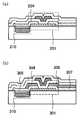
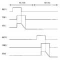
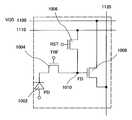
도 1은 본 발명의 하나의 실시 형태인 고체 이미지 센서의 화소 부분의 예를 예시하는 단면도이다. 도 1은 산화물 반도체를 포함하는 박막 트랜지스터가 전달 트랜지스터(101)로서 이용되는 예를 예시하고 있다. 증폭기 트랜지스터(131)는 단결정 실리콘 기판(100)을 이용하여 형성된 n-채널 벌크 트랜지스터를 이용하여 형성된다. 광전 변환 소자(110)는 n-타입 영역(112) 및 얇은 p-타입 영역(114)을 포함하는 포토다이오드를 형성하고, 전달 트랜지스터(101)의 소스 전극(104)에 접속된다. 신호 전하 저장부(116, 또한 플로팅 디퓨전으로 지칭됨)는 전달 트랜지스터(101)의 드레인 전극 아래에 형성된다. 전달 트랜지스터(101)는 산화물 반도체층이 채널 영역으로서 기능하는 톱-게이트 구조를 갖는다. 증폭기 트랜지스터(131)는 n-타입 영역들(132a 및 132b) 및 게이트 전극(138)을 포함하는 n-채널 벌크 트랜지스터이다. 증폭기 트랜지스터(131)의 게이트 전극(138)은 배선(154)을 통해 신호 전하 저장부(116)에 전기적으로 접속된다.1 is a cross-sectional view illustrating an example of a pixel portion of a solid state image sensor that is one embodiment of the present invention. 1 illustrates an example in which a thin film transistor including an oxide semiconductor is used as the
유의할 점은, 도 1에 예시된 구조에서, 벌크 트랜지스터의 게이트 절연층(136)은 박막 트랜지스터인 전달 트랜지스터(101)의 하지 절연층으로서 기능하고, 신호 전하 저장부(116)는 유전체로서 이용된 게이트 절연층(136)과 용량 소자를 형성한다는 점이다. 뿐만 아니라, 박막 트랜지스터의 게이트 절연층(118)은 벌크 트랜지스터의 층간 절연층의 일부로서 기능한다.Note that, in the structure illustrated in FIG. 1, the
채널 형성 영역에서 산화물 반도체를 포함하는 박막 트랜지스터는 하나의 예로서 톱-게이트 박막 트랜지스터로서 기재되어 있고, 그러나 박막 트랜지스터는 역스태거형 박막 트랜지스터 등의 보텀-게이트 박막 트랜지스터일 수 있다. 뿐만 아니라, 광으로 광전 변환 소자(110)를 조사하는 것이 필요하고, 따라서 전달 트랜지스터(101)의 소스 전극의 일부가 광전 변환 소자(110)의 광 수신부에 접속되는 예가 기재되어 있으며, 그러나 소스 전극은 광전 변환 소자(110)에게 상이한 방식으로 접속되도록 광-투과 도전성 재료를 이용하여 형성될 수도 있다. 예를 들면, 도 2의 (a)에 예시된 바와 같이, 광-투과 도전성 재료를 이용하여 형성되는 소스 전극(204)을 포함하는 트랜지스터(201)가 전달 트랜지스터로서 이용되는 경우에, 소스 전극은 광전 변환 소자(210)의 광 수신부의 일부 또는 전체에 접속될 수 있다. 다르게는, 도 2의 (b)에 예시된 바와 같이, 광전 변환 소자(310)에 대한 광 경로를 보장하기 위해, 낮은-저항성 금속층을 이용하여 형성된 소스 전극(304) 및 드레인 전극(306), 및 광-투과 도전성 재료층을 이용하여 형성된 버퍼층들(305 및 307)이 적층되는 트랜지스터(301)가 전달 트랜지스터로서 이용될 수 있다.The thin film transistor including the oxide semiconductor in the channel formation region is described as a top-gate thin film transistor as an example, but the thin film transistor may be a bottom-gate thin film transistor such as an inverted staggered thin film transistor. In addition, it is necessary to irradiate the
광전 변환 소자로 형성된 포토다이오드로서, n-타입 영역이 p-타입 단결정 실리콘 기판(SOI의 경우에, p-타입 단결정 실리콘층)에 형성되고 그 위에 얇은 p-타입 영역이 형성되는 소위 매립된 포토다이오드가 형성된다. 포토다이오드의 표면 위에 p-타입 영역이 형성됨으로써, 표면 위에서 발생하는 암전류로 인한 노이즈가 감소될 수 있다.A photodiode formed of a photoelectric conversion element, in which an n-type region is formed on a p-type single crystal silicon substrate (in the case of SOI, a p-type single crystal silicon layer) and a so-called buried photo in which a thin p-type region is formed thereon. Diode is formed. By forming a p-type region on the surface of the photodiode, noise due to dark current occurring on the surface can be reduced.
단결정 반도체 기판이 이용되는 하나의 예가 상기 기재되어 있지만, SOI 기판이 이용될 수도 있다. 뿐만 아니라, 벌크 트랜지스터의 구조는 상기 구조로 제한되지 않는다. 게이트 전극의 단부들에 측벽들이 제공되는 LDD(저 도핑 드레인) 구조 또는 저-저항성 실리사이드 등이 소스 영역 또는 드레인 영역의 일부에 형성되는 구조가 채용될 수도 있다.One example where a single crystal semiconductor substrate is used is described above, but an SOI substrate may be used. In addition, the structure of the bulk transistor is not limited to the above structure. An LDD (low doping drain) structure in which sidewalls are provided at ends of the gate electrode, or a structure in which a low-resistance silicide or the like is formed in a portion of the source region or the drain region may be employed.
증폭기 트랜지스터(131)에 전기적으로 접속되는 선택 트랜지스터는 화소부에 제공될 수 있다. 증폭기 트랜지스터 및 선택 트랜지스터는 실리콘 반도체 또는 산화물 반도체 중 어느 하나를 이용하여 형성될 수 있다. 유의할 점은, 증폭기 트랜지스터가 바람직하게는 더 높은 증폭률을 갖는 실리콘 반도체층을 포함하는 벌크 트랜지스터를 이용하여 형성된다는 점이다.The selection transistor electrically connected to the
다르게는, 절연층은 벌크 트랜지스터 위에 형성될 수 있고 그 위에 박막 트랜지스터가 형성될 수 있다. 예를 들면, 박막 트랜지스터를 이용하여 형성된 전달 트랜지스터가 벌크 트랜지스터를 이용하여 형성된 증폭기 트랜지스터 위에 제공되는 경우에, 화소당 요구되는 트랜지스터의 면적은 약 1/2 내지 2/3이므로, 통합 레벨이 개선될 수 있고, 수광 면적이 증가될 수 있으며, 노이즈가 감소될 수 있다. 도 3은 그러한 구조의 하나의 예를 예시하고 있다. 광전 변환 소자(510) 및 벌크 트랜지스터를 이용하여 형성된 증폭기 트랜지스터(531)는 하층으로서 형성되고, 박막 트랜지스터를 이용하여 형성된 전달 트랜지스터(501)는 절연막(541)이 개재된 상층으로서 형성된다. 광전 변환 소자 및 벌크 트랜지스터를 형성하는 단계 및 박막 트랜지스터를 형성하는 단계는 서로 분리될 수 있고, 따라서 단계들은 용이하게 제어될 수 있다. 유의할 점은, 신호 전하 저장부(516)를 형성하는 데 이용되는 용량 전극(540)이 바람직하게는 제공된다는 점이다.Alternatively, an insulating layer can be formed over the bulk transistor and a thin film transistor can be formed thereon. For example, in the case where a transfer transistor formed using a thin film transistor is provided over an amplifier transistor formed using a bulk transistor, the area of the transistor required per pixel is about 1/2 to 2/3, so that the integration level can be improved. Can be increased, the light receiving area can be increased, and noise can be reduced. 3 illustrates one example of such a structure. The
여기에서, 본 발명의 하나의 실시 형태에서, 산화물 반도체층을 포함하는 박막 트랜지스터가 제공되고, 고체 이미지 센서인 CMOS(상보형 금속 산화물 반도체) 이미지 센서의 일반적인 컴포넌트인 리세트 트랜지스터는 생략된다. 종래의 CMOS 이미지 센서에서, 신호 전하 저장부의 전위는 리세트 트랜지스터의 동작에 의해 초기화된다. 본 발명의 하나의 실시 형태에서, 신호 전하 저장부는 포토다이오드의 캐소드 전위로 초기화될 수 있다. 우선, 순방향 바이어스가 포토다이오드에 인가되고 전달 트랜지스터가 턴온되는 경우에, 신호 전하 저장부는 포토다이오드의 캐소드와 동일한 전위를 갖는다. 이어서, 역방향 바이어스가 포토다이오드에 인가되고 포토다이오드가 광으로 조사되는 경우에, 신호 전하 저장부의 전위는 방전에 의해 낮아진다. 이때, 전달 트랜지스터가 턴오프되고, 신호는 홀딩된 전위에 따라 증폭기 트랜지스터로부터 출력될 수 있다.Here, in one embodiment of the present invention, a thin film transistor including an oxide semiconductor layer is provided, and a reset transistor which is a general component of a CMOS (complementary metal oxide semiconductor) image sensor which is a solid state image sensor is omitted. In a conventional CMOS image sensor, the potential of the signal charge storage portion is initialized by the operation of the reset transistor. In one embodiment of the invention, the signal charge storage may be initialized to the cathode potential of the photodiode. First, when forward bias is applied to the photodiode and the transfer transistor is turned on, the signal charge storage has the same potential as the cathode of the photodiode. Then, when the reverse bias is applied to the photodiode and the photodiode is irradiated with light, the potential of the signal charge storage portion is lowered by the discharge. At this time, the transfer transistor is turned off, and the signal may be output from the amplifier transistor according to the held potential.
상기 구조들을 갖는 박막 트랜지스터 및 벌크 트랜지스터의 조합으로, 신호 전하 저장부는 더 긴 시간 동안 전위를 홀딩할 수 있고, 넓은 다이나믹 범위를 갖는 고체 이미지 센서의 화소부가 형성될 수 있다. 유의할 점은, 본 발명의 이러한 실시 형태를 실현하기 위해, 그 오프 전류가 크게 낮은 박막 트랜지스터가 바람직하게는 이용된다는 점이다. 그러한 박막 트랜지스터를 제조하기 위한 방법이 아래에 기재된다.With the combination of the thin film transistor and the bulk transistor having the above structures, the signal charge storage portion can hold the potential for a longer time, and the pixel portion of the solid state image sensor having a wide dynamic range can be formed. Note that, in order to realize such an embodiment of the present invention, a thin film transistor having a low off current is preferably used. A method for manufacturing such thin film transistors is described below.
본 발명의 하나의 실시 형태에서, 고체 이미지 센서의 화소부는 단결정 실리콘 반도체를 포함하는 벌크 트랜지스터 및 상당히 유리한 전기적 특성들을 갖는 산화물 반도체를 포함하는 박막 트랜지스터의 조합으로 형성된다. 그러므로, 산화물 반도체를 포함하는 박막 트랜지스터를 형성하기 위한 방법이 주로 상세하게 설명된다.In one embodiment of the present invention, the pixel portion of the solid state image sensor is formed of a combination of a bulk transistor comprising a single crystal silicon semiconductor and a thin film transistor comprising an oxide semiconductor having considerable advantageous electrical properties. Therefore, a method for forming a thin film transistor including an oxide semiconductor is mainly described in detail.
하나의 예로서, 도 1에 예시된 구조를 형성하기 위한 방법은 도 4의 (a) 내지 (c) 및 도 5의 (a) 내지 (c)의 단면도들을 참조하여 설명된다. 우선, 절연막(140, 또한 전계 산화막으로도 지칭됨)으로 분리되는 소자 형성 영역은 p-타입 단결정 실리콘 기판(100) 위에 형성된다. 소자 분리 영역은 실리콘의 로컬 산화(LOCOS), 얕은 트렌치 분리(STI) 등에 의해 형성될 수 있다.As one example, the method for forming the structure illustrated in FIG. 1 is described with reference to the cross-sectional views of FIGS. 4A to 4C and 5A to 5C. First, an element formation region separated by an insulating film 140 (also referred to as an electric field oxide film) is formed on the p-type single
여기에서, 기판은 단결정 실리콘 기판으로 제한되지 않는다. SOI(실리콘 온 절연체) 기판 등이 이용될 수 있다.Here, the substrate is not limited to the single crystal silicon substrate. SOI (silicon on insulator) substrates and the like can be used.
유의할 점은, 본 실시 형태에서, 매립된 포토다이오드 및 n-채널 벌크 트랜지스터가 이용되기 때문에, p-타입 단결정 실리콘 기판이 이용되지만, p-웰이 형성되는 경우에 n-타입 단결정 실리콘 기판이 이용될 수 있다는 점이다.Note that in this embodiment, a p-type single crystal silicon substrate is used because buried photodiodes and n-channel bulk transistors are used, but an n-type single crystal silicon substrate is used when p-wells are formed. Can be.
다음으로, 게이트 절연층(136)은 소자 형성 영역을 피복하도록 형성된다. 예를 들면, 산화 실리콘막은 열 처리로 단결정 실리콘 기판(100)에 제공된 소자 형성 영역의 표면의 산화에 의해 형성될 수 있다. 다르게는, 게이트 절연층(136)은, 열적 산화에 의한 산화 실리콘막의 형성, 및 질화 처리에 의한 산화 실리콘막의 표면의 질화에 의해, 산화 실리콘막 및 산화 질화 실리콘막의 적층 구조를 가질 수 있다.Next, the
또 하나의 방법으로서, 예를 들면, 단결정 실리콘 기판(100)에 제공된 소자 형성 영역의 표면 위에 형성된 고-밀도 플라즈마 처리를 갖는 산화 처리 또는 질화 처리에 의해, 산화 실리콘막 또는 질화 실리콘막은 게이트 절연층(136)으로서 형성될 수 있다. 또한, 고밀도 플라즈마 처리에 의한 소자 형성 영역의 표면 위에 산화 처리가 수행된 이후에, 질화 처리는 고-밀도 플라즈마 처리에 의해 수행될 수 있다. 이 경우에, 산화 실리콘막은 소자 형성 영역의 표면 위에 그리고 그에 접촉하여 형성되고, 산화 질화 실리콘막은 산화 실리콘막 위에 형성되어, 게이트 절연층(136)은 산화 실리콘막 및 산화 질화 실리콘막의 적층 구조를 갖는다.As another method, the silicon oxide film or the silicon nitride film is formed by the gate insulating layer, for example, by an oxidation process or a nitride process having a high-density plasma process formed on the surface of the element formation region provided in the single
다음으로, 도전층은 게이트 절연층(136)을 피복하도록 형성된다. 여기에서, 도전층(138a) 및 도전층(138b)은 순차적으로 적층된다. 물론, 도전층은 단층 구조 또는 2개 이상의 층들을 포함하는 적층 구조를 가져도 된다.Next, the conductive layer is formed to cover the
도전층들(138a 및 138b)은 탄탈륨(Ta), 텅스텐(W), 티타늄(Ti), 몰리브덴(Mo), 알루미늄(Al), 구리(Cu), 크롬(Cr) 또는 니오브(Nb)로부터 선택된 원소, 또는 그 원소를 주요 성분으로서 포함하는 합금 재료 또는 화합물 재료를 이용하여 형성될 수 있다. 다르게는, 상기 원소의 질화에 의해 얻어진 금속 질화막이 이용될 수 있다. 다르게는, 인 등의 불순물 원소로 도핑된 다결정 실리콘으로 전형화되는 반도체 재료가 이용될 수 있다.The
여기에서, 도전층(138a)이 탄탈륨 질화물을 이용하여 형성되고 도전층(138b)이 텅스텐을 이용하여 형성되는 적층 구조가 채용된다. 다르게는, 텅스텐 질화물, 몰리브덴 질화물 또는 티타늄 질화물의 단층 또는 그 적층된 막들은 도전층(138a)으로서 이용될 수 있고, 탄탈륨, 몰리브덴, 또는 티타늄의 단층 또는 그 적층막들은 도전층(138b)으로서 이용될 수 있다.Here, a laminated structure in which the
다음으로, 적층된 도전층들(138a 및 138b)을 선택적으로 에칭하여 제거함으로써, 도전층들(138a 및 138b)은 게이트 전극(138)이 형성되도록 게이트 절연층(136) 위에 부분적으로 남겨진다.Next, by selectively etching and removing the stacked
다음으로, 레지스트 마스크는 소자 형성 영역을 제외한 영역들을 피복하도록 선택적으로 형성되고, n-타입 영역들(132a 및 132b)은 레지스트 마스크 및 게이트 전극(138)을 마스크들로서 이용하여 불순물 원소의 유입에 의해 형성된다. 여기에서, n-채널 벌크 트랜지스터가 형성되므로, n-타입 도전성을 부여하는 불순물 원소(예를 들면, 인(P) 또는 비소(As))가 불순물 원소로서 이용될 수 있다.Next, a resist mask is selectively formed to cover regions other than the element formation region, and the n-
이어서, 광전 변환 소자인 포토다이오드를 형성하기 위해, 레지스트 마스크가 선택적으로 형성된다. 우선, p-n 접합이 n-타입 도전성(예를 들면, 인(P) 또는 비소(As))을 부여하는 불순물 원소의 p-타입 단결정 실리콘 기판으로의 유입에 의해 형성된 이후에, p-타입 도전성(예를 들면, 붕소(B))을 부여하는 불순물 원소가 n-타입 영역의 표면층으로 유입되고, 따라서 매립된 포토다이오드가 형성될 수 있다.Subsequently, a resist mask is selectively formed to form a photodiode as a photoelectric conversion element. First, after the pn junction is formed by the inflow of an impurity element imparting n-type conductivity (e.g., phosphorus (P) or arsenic (As)) to the p-type single crystal silicon substrate, the p-type conductivity ( For example, an impurity element imparting boron (B) is introduced into the surface layer of the n-type region, and thus a buried photodiode can be formed.
이러한 스테이지에서, 도 4의 (a)의 우측에 예시된 벌크 트랜지스터 및 도 4의 (a)의 좌측에 예시된 포토다이오드의 구조들이 완성된다.At this stage, the structures of the bulk transistor illustrated on the right side of FIG. 4A and the photodiode illustrated on the left side of FIG. 4A are completed.
다음으로, 산화물 반도체층이 채널 영역으로서 이용되는 박막 트랜지스터를 형성하기 위한 방법이 기재된다.Next, a method for forming a thin film transistor in which an oxide semiconductor layer is used as a channel region is described.
이러한 실시 형태에서, 박막 트랜지스터는 단결정 실리콘 기판(100) 위에 제공된 벌크 트랜지스터의 게이트 절연층(136) 위에 형성된다. 즉, 게이트 절연층(136)은 박막 트랜지스터의 하지막, 및 벌크 트랜지스터의 게이트 절연층으로서 기능할 수 있다. 유의할 점은, 절연층은 이하의 방법에 의해 형성될 수 있고 적층된 층들은 하지막으로 이용될 수도 있다는 점이다.In this embodiment, the thin film transistor is formed over the
산화물 반도체층과 접촉하고 있는 절연층으로서, 산화 실리콘층, 산화 질화 실리콘층, 산화 알루미늄층, 또는 산화 질화 알루미늄층 등의 산화물 절연층이 바람직하게 이용된다. 절연층을 형성하기 위한 방법으로서, 플라즈마-인핸스드 CVD, 스퍼터링 등이 이용될 수 있다. 절연층에 다량의 수소가 포함되지 않도록, 절연층은 바람직하게는 스퍼터링에 의해 형성된다.As the insulating layer in contact with the oxide semiconductor layer, an oxide insulating layer such as a silicon oxide layer, a silicon oxynitride layer, an aluminum oxide layer, or an aluminum oxynitride layer is preferably used. As a method for forming the insulating layer, plasma-enhanced CVD, sputtering, or the like can be used. The insulating layer is preferably formed by sputtering so that a large amount of hydrogen is not contained in the insulating layer.
산화 실리콘층이 절연층으로서 스퍼터링에 의해 형성되는 하나의 예가 기재되어 있다. 단결정 실리콘 기판(100)이 처리 챔버에 전달되고, 수소 및 습기가 제거된 고-순도 산소를 포함하는 스퍼터링 가스가 유입되며, 실리콘 타겟이 이용되는 방식으로, 산화 실리콘층이 절연층으로서 단결정 실리콘 기판(100) 위에 피착된다. 뿐만 아니라, 단결정 실리콘 기판(100)은 실온에 있거나 가열될 수도 있다.One example is described in which a silicon oxide layer is formed by sputtering as an insulating layer. The single
예를 들면, 산화 실리콘층은 이하의 조건 하에서 RF 스퍼터링에 의해 피착된다. 석영(바람직하게는 합성 석영)이 타겟으로서 이용되고, 기판의 온도는 108℃이며, 기판과 타겟 사이의 거리(T-S 거리)는 60mm이고, 압력은 0.4Pa이며, 고-주파수 전력은 1.5kW이고, 대기는 산소 및 비소(25sccm의 산소 유속 : 25sccm의 비소 유속 = 1:1)를 포함하며, 두께는 100nm이다. 석영 대신에, 실리콘은 산화 실리콘층을 피착하기 위한 타겟으로서 이용될 수 있다. 이 경우에, 산소 또는 산소와 비소의 혼합 가스는 스퍼터링 가스로서 이용된다.For example, a silicon oxide layer is deposited by RF sputtering under the following conditions. Quartz (preferably synthetic quartz) is used as the target, the temperature of the substrate is 108 ° C., the distance between the substrate and the target (TS distance) is 60 mm, the pressure is 0.4 Pa, the high-frequency power is 1.5 kW and , The atmosphere contains oxygen and arsenic (25 sccm oxygen flow rate: 25 sccm arsenic flow rate 1: 1), the thickness is 100nm. Instead of quartz, silicon can be used as a target for depositing a silicon oxide layer. In this case, oxygen or a mixed gas of oxygen and arsenic is used as the sputtering gas.
이 경우에, 수소, 수산기, 또는 습기가 절연층에 포함되지 않도록, 처리 챔버에 남아있는 습기가 제거되는 동안에, 절연층을 형성하는 것이 바람직하다.In this case, it is preferable to form an insulating layer while the moisture remaining in the processing chamber is removed so that hydrogen, hydroxyl groups, or moisture are not included in the insulating layer.
처리 챔버에 남아있는 습기를 제거하기 위해, 바람직하게는 흡착 진공 펌프가 이용된다. 예를 들면, 바람직하게는 크라이오펌프, 이온 펌프, 또는 티타늄 승화 펌프가 이용된다. 배기 수단으로서, 콜드 트랩이 추가되는 터보 펌프가 이용될 수 있다. 예를 들면, 수소 원자, 물(H2O)과 같이 수소 원자를 포함하는 화합물 등은 크라이오펌프를 이용하여 처리 챔버로부터 배기된다. 그러므로, 처리 챔버에서 피착되는 절연층에 포함된 불순물의 농도가 낮아질 수 있다.In order to remove moisture remaining in the processing chamber, an adsorption vacuum pump is preferably used. For example, a cryopump, an ion pump, or a titanium sublimation pump is preferably used. As the exhaust means, a turbo pump to which a cold trap is added can be used. For example, a hydrogen atom, a compound containing a hydrogen atom such as water (H2 O), and the like are exhausted from the processing chamber using a cryopump. Therefore, the concentration of impurities contained in the insulating layer deposited in the processing chamber can be lowered.
절연층의 피착에 이용되는 스퍼터링 가스로서, 바람직하게는 수소, 물, 수산기, 또는 수소화물 등의 불순물이 대략 ppm 또는 ppb의 농도까지 제거되는 고-순도 가스가 이용된다.As the sputtering gas used for the deposition of the insulating layer, a high-purity gas is preferably used in which impurities such as hydrogen, water, hydroxyl groups, or hydrides are removed to a concentration of approximately ppm or ppb.
스퍼터링의 예들은 고-주파수 전력 소스가 스퍼터링 전력 소스에 이용되는 RF 스퍼터링, DC 전력 소스가 이용되는 DC 스퍼터링, 및 바이어스가 펄스 방식으로 인가되는 펄스형 DC 스퍼터링을 포함한다. RF 스퍼터링은 주로 절연막이 피착되는 경우에 이용되고, DC 스퍼터링은 주로 도전막이 피착되는 경우에 이용된다.Examples of sputtering include RF sputtering where a high-frequency power source is used for the sputtering power source, DC sputtering where a DC power source is used, and pulsed DC sputtering where bias is applied in a pulsed manner. RF sputtering is mainly used when an insulating film is deposited, and DC sputtering is mainly used when a conductive film is deposited.
뿐만 아니라, 상이한 재료들의 복수의 타겟들이 설정될 수 있는 멀티-소스 스퍼터링 장치도 있다. 멀티-소스 스퍼터링 장치에 있어서, 상이한 재료들의 막이 동일한 챔버에 적층되도록 피착되거나, 복수 종류의 재료들의 막이 동일한 챔버 내에서 동시에 전기 방전에 의해 피착될 수 있다.In addition, there are multi-source sputtering apparatus in which a plurality of targets of different materials can be set. In a multi-source sputtering apparatus, films of different materials may be deposited to be stacked in the same chamber, or films of plural kinds of materials may be deposited by electric discharge simultaneously in the same chamber.
뿐만 아니라, 챔버 내부에 자석 시스템이 제공되고 마그네트론 스퍼터링에 이용되는 스퍼터링 장치, 및 글로우 방전을 이용하지 않고 마이크로파를 이용하여 생성된 플라즈마가 이용되는 ECR 스퍼터링에 이용되는 스퍼터링 장치가 있다.In addition, there is a sputtering apparatus provided with a magnet system inside the chamber and used for magnetron sputtering, and a sputtering apparatus used for ECR sputtering using plasma generated using microwaves without using glow discharge.
또한, 스퍼터링을 이용하는 피착 방법으로서, 피착 동안에 타겟 물질과 스퍼터링 가스 성분이 서로 화학적으로 반응되어 그 얇은 화합물 막을 형성하는 반응성 스퍼터링, 또는 피착 동안에 전압이 기판에 또한 인가되는 바이어스 스퍼터링이 이용될 수 있다.In addition, as a deposition method using sputtering, reactive sputtering in which the target material and the sputtering gas component chemically react with each other during deposition to form a thin compound film, or bias sputtering in which a voltage is also applied to the substrate during deposition, may be used.
또한, 절연층은 적층 구조를 가질 수 있다. 예를 들면, 절연층은 질화 실리콘층, 질화 산화 실리콘층, 질화 알루미늄층, 또는 질화 산화 알루미늄층 등의 질화물 절연층, 및 상기 산화물 절연층이 기판 측으로부터 그 순서로 적층되는 적층 구조를 가질 수 있다.In addition, the insulating layer may have a laminated structure. For example, the insulating layer may have a nitride insulating layer such as a silicon nitride layer, a silicon nitride oxide layer, an aluminum nitride layer, or an aluminum nitride oxide layer, and a laminate structure in which the oxide insulating layer is laminated in that order from the substrate side. have.
예를 들면, 질화 실리콘층은 수소 및 습기가 제거된 고-순도 질소를 포함하는 스퍼터링 가스가 산화 실리콘층과 기판 사이에 유입되고 실리콘 타겟이 이용되는 방식으로 피착된다. 또한, 이 경우에도, 산화 실리콘층의 경우에서와 같이, 처리 챔버 내에 남아있는 습기가 제거되어 있는 동안에 질화 실리콘층을 피착하는 것이 바람직하다.For example, the silicon nitride layer is deposited in such a manner that a sputtering gas containing hydrogen and high-purity nitrogen from which moisture has been removed is introduced between the silicon oxide layer and the substrate and the silicon target is used. Also in this case, as in the case of the silicon oxide layer, it is preferable to deposit the silicon nitride layer while the moisture remaining in the processing chamber is removed.
또한, 질화 실리콘층이 피착되는 경우에도, 기판은 피착 시에 가열될 수 있다.Further, even when the silicon nitride layer is deposited, the substrate can be heated at the time of deposition.
질화 실리콘층 및 산화 실리콘층이 절연층으로서 적층되는 경우에, 질화 실리콘층 및 산화 실리콘층은 공통 실리콘 타겟을 이용하여 동일한 처리 챔버 내에서 피착될 수 있다. 우선, 질화 실리콘층은 질소를 포함하는 스퍼터링 가스가 유입되고 처리 챔버 위에 장착된 실리콘 타겟이 이용되는 방식으로 피착된다. 이어서, 산화 실리콘층은 가스가 산소를 포함하는 스퍼터링 가스로 변경되고 동일한 실리콘 타겟이 이용되는 방식으로 피착된다. 질화 실리콘층 및 산화 실리콘층은 공기로의 노출없이 연속적으로 피착될 수 있고, 따라서 질화 실리콘층의 표면 위에서 수소 또는 습기 등의 불순물의 흡착이 방지될 수 있다.In the case where the silicon nitride layer and the silicon oxide layer are laminated as the insulating layer, the silicon nitride layer and the silicon oxide layer can be deposited in the same processing chamber using a common silicon target. First, the silicon nitride layer is deposited in such a manner that a sputtering gas containing nitrogen is introduced therein and a silicon target mounted on the processing chamber is used. The silicon oxide layer is then deposited in such a way that the gas is changed to a sputtering gas containing oxygen and the same silicon target is used. The silicon nitride layer and silicon oxide layer can be deposited continuously without exposure to air, and thus adsorption of impurities such as hydrogen or moisture on the surface of the silicon nitride layer can be prevented.
이어서, 2 내지 200nm의 두께를 갖는 산화물 반도체막이 절연층(본 실시 형태에서, 게이트 절연층(136)) 위에 형성된다.Next, an oxide semiconductor film having a thickness of 2 to 200 nm is formed over the insulating layer (
수소, 수산기 및 습기가 산화물 반도체막에 가능한 한 적게 포함되도록, 단결정 실리콘 기판(100) 위에 흡착되는 수소 또는 습기 등의 불순물은, 피착을 위한 사전처리로서, 스퍼터링 장치의 사전가열 챔버 내에서 단결정 실리콘 기판(100)의 사전 가열에 의해 제거되고 배기되는 것이 바람직하다. 사전가열 챔버에 제공된 배기 수단으로서, 크라이오펌프가 바람직하다. 유의할 점은, 사전가열 처리가 생략될 수 있다는 점이다. 뿐만 아니라, 사전가열은 나중에 형성될 박막 트랜지스터의 게이트 절연층(118)의 피착 이전에 수행되거나, 나중에 형성될 소스 전극 및 드레인 전극으로서 기능하는 도전층의 피착 이전에 수행될 수도 있다.Impurities such as hydrogen or moisture adsorbed on the single
유의할 점은, 산화물 반도체막이 스퍼터링에 의해 피착되기 이전에, 절연층의 표면 위의 먼지는 바람직하게는 비소 가스가 유입되고 플라즈마가 생성되는 역방향 스퍼터링에 의해 제거된다는 점이다. 역방향 스퍼터링은 비소 분위기에서 RF 전력 소스를 이용하여 전압이 기판 측에 인가되고 이온화된 비소가 기판과 충돌하여 기판 표면이 개질되는 방법을 지칭한다. 유의할 점은, 질소, 헬륨, 산소 등이 비소 대신에 이용될 수 있다는 점이다.Note that, before the oxide semiconductor film is deposited by sputtering, the dust on the surface of the insulating layer is preferably removed by reverse sputtering in which arsenic gas is introduced and plasma is generated. Reverse sputtering refers to a method in which a voltage is applied to a substrate side using an RF power source in an arsenic atmosphere and ionized arsenic collides with the substrate to modify the substrate surface. Note that nitrogen, helium, oxygen and the like can be used in place of arsenic.
산화물 반도체막은 스퍼터링에 의해 피착된다. 산화물 반도체막으로서, In-Sn-Ga-Zn-O 막 등의 4-성분 금속 산화물, In-Ga-Zn-O 막, In-Sn-Zn-O 막, In-Al-Zn-O 막, Sn-Ga-Zn-O 막, Al-Ga-Zn-O 막, 또는 Sn-Al-Zn-O 막 등의 3-성분 금속 산화물, 또는 In-Zn-O 막, Sn-Zn-O 막, Al-Zn-O 막, Zn-Mg-O 막, Sn-Mg-O 막, In-Mg-O 막, In-O 막, Sn-O 막, 또는 Zn-O 막 등의 2-성분 금속 산화물이 이용될 수 있다. 또한, SiO2는 상기 산화물 반도체막에 포함될 수 있다.An oxide semiconductor film is deposited by sputtering. As the oxide semiconductor film, 4-component metal oxides such as In-Sn-Ga-Zn-O films, In-Ga-Zn-O films, In-Sn-Zn-O films, In-Al-Zn-O films, 3-component metal oxides such as Sn-Ga-Zn-O films, Al-Ga-Zn-O films, or Sn-Al-Zn-O films, or In-Zn-O films, Sn-Zn-O films, 2-component metal oxides such as Al-Zn-O films, Zn-Mg-O films, Sn-Mg-O films, In-Mg-O films, In-O films, Sn-O films, or Zn-O films This can be used. In addition, SiO2 may be included in the oxide semiconductor film.
산화물 반도체막으로서, InMO3(ZnO)m(m>0)에 의해 표현되는 박막이 이용될 수 있다. 여기에서, M은 Ga, Al, Mn, 또는 Co로부터 선택되는 하나 이상의 금속 원소들을 나타낸다. 예를 들면, M은 Ga, Ga 및 Al, Ga 및 Mn, Ga 및 Co 등일 수 있다. 그 조성식이 InMO3(ZnO)m(m>0)에 의해 표현되는 산화물 반도체막들 중에서, M으로서 Ga를 포함하는 산화물 반도체는 In-Ga-Zn-O계 산화물 반도체로서 지칭되고, In-Ga-Zn-O계 산화물 반도체의 박막은 또한 In-Ga-Zn-O계 막으로 지칭된다.As the oxide semiconductor film, a thin film represented by InMO3 (ZnO)m (m> 0) can be used. Here, M represents one or more metal elements selected from Ga, Al, Mn, or Co. For example, M may be Ga, Ga and Al, Ga and Mn, Ga and Co and the like. Of the oxide semiconductor films whose composition formula is represented by InMO3 (ZnO)m (m> 0), an oxide semiconductor containing Ga as M is referred to as an In—Ga—Zn—O based oxide semiconductor, and is referred to as In—Ga. Thin films of -Zn-O based oxide semiconductors are also referred to as In-Ga-Zn-O based films.
이러한 실시 형태에서, 산화물 반도체막은 In-Ga-Zn-O계 금속 산화물 타겟을 이용하여 스퍼터링에 의해 피착된다. 다르게는, 산화물 반도체막은 희가스(통상적으로는 비소) 분위기, 산소 분위기, 또는 희가스(통상적으로는 비소) 및 산소를 포함하는 분위기에서 스퍼터링에 의해 피착될 수 있다.In this embodiment, the oxide semiconductor film is deposited by sputtering using an In—Ga—Zn—O-based metal oxide target. Alternatively, the oxide semiconductor film may be deposited by sputtering in a rare gas (usually arsenic) atmosphere, an oxygen atmosphere, or an atmosphere containing rare gas (usually arsenic) and oxygen.
산화물 반도체막의 피착에 이용되는 스퍼터링 가스로서, 바람직하게는 수소, 물, 수산기 또는 수소화물 등의 불순물이 대략 ppm 또는 ppb의 농도까지 제거되는 고-순도 가스가 이용된다.As the sputtering gas used for the deposition of the oxide semiconductor film, a high-purity gas is preferably used in which impurities such as hydrogen, water, hydroxyl groups or hydrides are removed to a concentration of approximately ppm or ppb.
스퍼터링에 의해 산화물 반도체막을 형성하는 데 이용되는 타겟으로서, 주요 성분으로서 아연 산화물을 포함하는 금속 산화물 타겟이 이용될 수 있다. 예를 들면, In2O3:Ga2O3:ZnO=1:1:1(몰 비율)의 조성 비율을 갖는 금속 산화물 타겟이 이용될 수 있다. 다르게는, In2O3:Ga2O3:ZnO=1:1:2(몰 비율)의 조성 비율을 갖는 금속 산화물 타겟이 이용될 수 있다. 금속 산화물 타겟의 필링 레이트(filling rate)는 90 내지 100%이고, 바람직하게는 95 내지 99.9%이다. 높은 필링 레이트를 갖는 금속 산화물 타겟을 이용함으로써, 피착된 산화물 반도체막은 높은 밀도를 갖는다.As the target used for forming the oxide semiconductor film by sputtering, a metal oxide target containing zinc oxide as the main component can be used. For example, a metal oxide target having a composition ratio of In2 O3 : Ga2 O3 : ZnO = 1: 1: 1 (molar ratio) may be used. Alternatively, a metal oxide target having a composition ratio of In2 O3 : Ga2 O3 : ZnO = 1: 1: 2 (molar ratio) may be used. The filling rate of the metal oxide target is 90 to 100%, preferably 95 to 99.9%. By using a metal oxide target having a high filling rate, the deposited oxide semiconductor film has a high density.
감소된 압력 상태에서 유지된 처리 챔버에 기판이 홀딩되고, 처리 챔버에 유지되는 습기가 제거되며, 수소 및 습기가 제거되는 스퍼터링 가스가 유입되고, 금속 산화물이 타겟으로 이용되는 방식으로, 산화물 반도체막이 절연층 위에 피착된다. 처리 챔버에 남아있는 습기를 제거하기 위해, 바람직하게는 흡착 진공 펌프가 이용된다. 예를 들면, 바람직하게는 크라이오펌프, 이온 펌프, 또는 티타늄 승화 펌프가 이용된다. 배기 수단으로서, 콜드 트랩이 추가되는 터보 펌프가 이용될 수 있다. 예를 들면, 수소 원자, 물(H2O) 등의 수소 원자를 포함하는 화합물 등은 크라이오펌프를 이용하여 처리 챔버로부터 배기된다. 그러므로, 처리 챔버 내에 피착된 산화물 반도체막에 포함된 불순물의 농도가 낮아질 수 있다. 또한, 산화물 반도체막이 피착되는 경우에, 기판이 가열될 수 있다.The oxide semiconductor film is formed in such a manner that the substrate is held in the processing chamber maintained at a reduced pressure, moisture retained in the processing chamber is removed, a sputtering gas from which hydrogen and moisture are removed is introduced, and a metal oxide is used as the target. It is deposited on the insulating layer. In order to remove moisture remaining in the processing chamber, an adsorption vacuum pump is preferably used. For example, a cryopump, an ion pump, or a titanium sublimation pump is preferably used. As the exhaust means, a turbo pump to which a cold trap is added can be used. For example, a compound containing a hydrogen atom such as a hydrogen atom, water (H2 O), or the like is exhausted from the processing chamber using a cryopump. Therefore, the concentration of impurities contained in the oxide semiconductor film deposited in the processing chamber can be lowered. In addition, when the oxide semiconductor film is deposited, the substrate can be heated.
피착 조건의 하나의 예로서, 이하의 조건이 채용된다. 기판 온도는 실온이고, 기판과 타겟 간의 거리는 110mm이며, 압력은 0.4 Pa이고, 직류(DC) 전력은 0.5kW이며, 산소 및 비소를 포함하는 분위기(산소의 유속은 15sccm이고 비소의 유속은 30sccm이다)가 이용된다. 유의할 점은, 피착 시 생성되는 파우더형 물질들(또한 입자 또는 먼지로 지칭됨)이 감소될 수 있고 막 두께가 일정할 수 있기 때문에, 펄스형 직류(DC) 전력이 이용되는 것이 바람직하다는 점이다. 산화물 반도체막의 두께는 바람직하게는 5 내지 30nm이다. 유의할 점은, 산화물 반도체막의 적절한 두께는 산화물 반도체 재료에 따라 상이하고, 두께는 재료에 따라 적절히 설정될 수 있다는 점이다.As one example of deposition conditions, the following conditions are employed. The substrate temperature is room temperature, the distance between the substrate and the target is 110mm, the pressure is 0.4 Pa, the direct current (DC) power is 0.5kW, the atmosphere containing oxygen and arsenic (the flow rate of oxygen is 15sccm and the flow rate of arsenic is 30sccm) ) Is used. Note that the pulsed direct current (DC) power is preferably used because the powdery materials (also referred to as particles or dust) produced during deposition can be reduced and the film thickness can be constant. . The thickness of the oxide semiconductor film is preferably 5 to 30 nm. Note that the appropriate thickness of the oxide semiconductor film is different depending on the oxide semiconductor material, and the thickness can be appropriately set depending on the material.
이어서, 산화물 반도체막은 제1 포토리소그래피 프로세스 및 에칭 프로세스(도 4의 (b) 참조)에 의해 섬 형상의 산화물 반도체층(102)으로 처리된다.Next, the oxide semiconductor film is processed into an island-shaped
유의할 점은, 섬 형상의 산화물 반도체층의 형성에 이용되는 레지스트 마스크가 잉크젯 방법에 의해 형성될 수 있다는 점이다. 레지스트 마스크가 잉크젯 방법에 의해 형성되는 경우, 포토마스크가 이용되지 않고, 따라서 제조 비용이 감소될 수 있다. 또한, 산화물 반도체막의 에칭으로서, 건식 에칭, 습식 에칭, 또는 이들 양쪽 모두가 채용될 수 있다.Note that the resist mask used for forming the island-shaped oxide semiconductor layer can be formed by the inkjet method. When the resist mask is formed by the inkjet method, the photomask is not used, and thus the manufacturing cost can be reduced. In addition, as the etching of the oxide semiconductor film, dry etching, wet etching, or both can be employed.
건식 에칭에 이용된 에칭 가스로서, 염소를 포함하는 가스(염소(Cl2), 염화붕소(BCl3), 염화 실리콘(SiCl4), 또는 사염화탄소(CCl4) 등의 염소계 가스)가 바람직하게는 이용된다.As the etching gas used for the dry etching, a gas containing chlorine (chlorine gas such as chlorine (Cl2 ), boron chloride (BCl3 ), silicon chloride (SiCl4 ), or carbon tetrachloride (CCl4 )) is preferable. Is used.
다르게는, 불소 포함 가스(사불화탄소(CF4), 육불화유황(SF6), 삼불화질소(NF3), 또는 트리플루오로메탄(CHF3) 등의 불소계 가스), 브롬화수소(HBr), 산소(O2), 헬륨(He) 또는 비소(Ar) 등의 희가스가 첨가된 이들 가스들 중 임의의 것 등이 이용될 수 있다.Alternatively, fluorine-containing gas (carbon tetrafluoride (CF4 ), sulfur hexafluoride (SF6 ), fluorine-based gas such as nitrogen trifluoride (NF3 ), or trifluoromethane (CHF3 )), hydrogen bromide (HBr) Any of these gases to which a rare gas such as oxygen (O2 ), helium (He), or arsenic (Ar) is added may be used.
건식 에칭으로서, 평행한 플레이트 RIE(반응성 이온 에칭) 또는 ICP(유도성으로 결합된 플라즈마) 에칭이 이용될 수 있다. 원하는 형태를 갖도록 막을 에칭하기 위해, 에칭 조건들(코일-형태의 전극에 인가되는 전력량, 기판 측 위의 전극에 인가되는 전력량, 기판 측 위의 전극의 온도 등)이 적절하게 조정된다.As a dry etching, parallel plate RIE (reactive ion etching) or ICP (inductively coupled plasma) etching can be used. To etch the film to have the desired shape, the etching conditions (the amount of power applied to the coil-shaped electrode, the amount of power applied to the electrode on the substrate side, the temperature of the electrode on the substrate side, etc.) are appropriately adjusted.
습식 에칭에 이용되는 에칭액으로서, 인산, 아세트산 및 질산의 혼합물, 암모니아 과산화수소 혼합물(31wt%의 과산화수소 용액: 28wt%의 암모니아수: 물 = 5:2:2) 등에 의해 얻어진 용액이 이용될 수 있다. 다르게는, ITO-07N(KANTO CHEMICAL CO., INC.에 의해 생산됨)이 이용될 수 있다.As the etchant used for the wet etching, a solution obtained by a mixture of phosphoric acid, acetic acid and nitric acid, ammonia hydrogen peroxide mixture (31 wt% hydrogen peroxide solution: 28 wt% aqueous ammonia: water = 5: 2: 2) and the like can be used. Alternatively, ITO-07N (produced by KANTO CHEMICAL CO., INC.) May be used.
습식 에칭에 이용되는 에칭액은 세척에 의해 에칭된 재료와 함께 제거된다. 제거된 재료를 포함하는 에칭액의 폐기물 액체는 정화될 수 있고, 폐기물 액체에 포함된 재료가 재이용될 수 있다. 산화물 반도체층에 포함된 인듐 등의 재료가 에칭 후에 폐기물 액체로부터 수집되어 재이용되는 경우에, 자원들이 효율적으로 이용될 수 있고 비용이 감소될 수 있다.The etchant used for the wet etching is removed together with the etched material by washing. The waste liquid of the etchant including the removed material can be purified, and the material contained in the waste liquid can be reused. When a material such as indium contained in the oxide semiconductor layer is collected from the waste liquid after etching and reused, resources can be efficiently used and the cost can be reduced.
원하는 형태를 갖도록 산화물 반도체막을 에칭하기 위해, 에칭 조건들(에칭액, 에칭 시간, 온도 등)은 재료에 따라 적절하게 조정된다.In order to etch the oxide semiconductor film to have a desired shape, the etching conditions (etching liquid, etching time, temperature, etc.) are appropriately adjusted according to the material.
본 실시 형태에서, 산화물 반도체막은 인산, 아세트산 및 질산이 에칭액으로 혼합된 용액을 이용하여, 습식 에칭에 의해 섬 형상의 산화물 반도체층(102)으로 처리된다.In this embodiment, the oxide semiconductor film is treated with an island-shaped
본 실시 형태에서, 산화물 반도체층(102)은 희가스(예를 들면, 질소, 헬륨, 네온 또는 비소) 분위기에서 제1 열처리를 받는다. 제1 열 처리의 온도는 400 내지 750℃이고, 바람직하게는 400℃ 이상 기판의 변형점 미만이다. 여기에서, 기판이 일종의 열 처리 장치인 전기로에 넣어진 후에, 산화물 반도체층은 질소 분위기에서 1시간 동안 450℃에서 열 처리를 받는다. 온도가 열 처리 온도로부터 낮아지는 경우에, 분위기는 산소 분위기로 변경될 수 있다. 제1 열처리를 통해, 산화물 반도체층(102)이 탈수화되거나 탈수소화될 수 있다.In this embodiment, the
열 처리 장치는 전기로로 제한되지 않고, 저항 히터 등의 히터로부터 열 전도 또는 열 방사에 의해 처리될 피처리물을 가열하기 위한 장치를 구비할 수 있다. 예를 들면, GRTA(가스 급속 열적 어닐링) 장치 또는 LRTA(램프 급속 열적 어닐링) 장치 등의 RTA(급속 열적 어닐링) 장치가 이용될 수 있다. LRTA 장치는 할로겐 램프, 금속 핼라이드 램프, 크세논 아크 램프, 탄소 아크 램프, 고압 나트륨 램프, 또는 고압 수은 램프 등의 램프로부터 방출되는 광(전자기파)의 방사에 의해 처리될 피처리물을 가열하기 위한 장치이다. GRTA 장치는 고온 가스를 이용하여 열 처리가 수행되는 장치이다. 가스로서, 질소, 또는 비소 등의 희가스와 같이, 열 처리에 의해 처리될 피처리물과 반응하지 않는 비활성 가스가 이용된다.The heat treatment apparatus is not limited to an electric furnace, and may include an apparatus for heating a workpiece to be treated by heat conduction or heat radiation from a heater such as a resistance heater. For example, a rapid thermal annealing (RTA) apparatus such as a GRTA (gas rapid thermal annealing) apparatus or an LRTA (lamp rapid thermal annealing) apparatus may be used. The LRTA apparatus is for heating a workpiece to be treated by radiation of light (electromagnetic waves) emitted from a lamp such as a halogen lamp, a metal halide lamp, a xenon arc lamp, a carbon arc lamp, a high pressure sodium lamp, or a high pressure mercury lamp. Device. GRTA apparatus is a apparatus in which heat treatment is performed using hot gas. As the gas, an inert gas that does not react with the object to be treated by heat treatment, such as a rare gas such as nitrogen or arsenic, is used.
예를 들면, 제1 열 처리로서, GRTA는 이하와 같이 수행될 수 있다. 기판은 이동되고, 650 내지 700℃의 고온에서 가열된 비활성 가스에 넣어지며, 수 분 동안 가열되고, 이동되어 고온에서 가열된 비활성 가스로부터 빼내어진다. GRTA는 짧은 시간에 고온 열 처리를 가능하게 한다.For example, as the first heat treatment, GRTA can be performed as follows. The substrate is moved, placed in an inert gas heated at a high temperature of 650 to 700 ° C., heated for several minutes, and moved out of the inert gas heated at a high temperature. GRTA enables high temperature heat treatment in a short time.
유의할 점은, 제1 열 처리에서, 물, 수소 등이 질소, 헬륨, 네온 또는 비소 등의 분위기 가스에 포함되지 않는 것이 바람직하다는 점이다. 또한, 분위기 가스의 순도는 바람직하게는 6N(99.9999%) 이상, 더 바람직하게는 7N(99.99999%) 이상(즉, 불순물 농도는 1ppm 이하, 바람직하게는 0.1ppm 이하이다)이다. 산소가 분위기 가스로서 이용되는 경우에, 분위기 가스는 바람직하게는 유사한 순도를 갖는다.Note that, in the first heat treatment, it is preferable that water, hydrogen, or the like is not contained in an atmosphere gas such as nitrogen, helium, neon, or arsenic. In addition, the purity of the atmospheric gas is preferably 6N (99.9999%) or more, more preferably 7N (99.99999%) or more (that is, the impurity concentration is 1 ppm or less, preferably 0.1 ppm or less). When oxygen is used as the atmosphere gas, the atmosphere gas preferably has similar purity.
또한, 산화물 반도체층은 결정화되어 있고, 산화물 반도체층의 결정 구조는 일부 경우들에서, 제1 열처리의 조건 또는 산화물 반도체층의 재료에 따라 미결정(microcrystalline) 구조 또는 다결정 구조로 변경된다. 예를 들면, 산화물 반도체층은 90% 이상 또는 80% 이상의 결정화율을 갖는 미결정(microcrystalline) 산화물 반도체층이 되도록 결정화될 수도 있다. 또한, 제1 열처리의 조건 또는 산화물 반도체층의 재료에 따라, 산화물 반도체층은 어떠한 결정 성분도 포함하지 않는 비정질 산화물 반도체층이 될 수 있다. 산화물 반도체층은 미결정(microcrystalline)부(1 내지 20nm, 통상적으로는 2 내지 4nm의 입자 직경을 가짐)가 비정질 산화물 반도체에 혼합되는 산화물 반도체층이 될 수 있다.In addition, the oxide semiconductor layer is crystallized, and in some cases, the crystal structure of the oxide semiconductor layer is changed into a microcrystalline structure or a polycrystalline structure depending on the conditions of the first heat treatment or the material of the oxide semiconductor layer. For example, the oxide semiconductor layer may be crystallized to be a microcrystalline oxide semiconductor layer having a crystallization rate of 90% or more or 80% or more. Further, depending on the conditions of the first heat treatment or the material of the oxide semiconductor layer, the oxide semiconductor layer may be an amorphous oxide semiconductor layer containing no crystal component. The oxide semiconductor layer may be an oxide semiconductor layer in which microcrystalline portions (having a particle diameter of 1 to 20 nm, typically 2 to 4 nm) are mixed with an amorphous oxide semiconductor.
뿐만 아니라, 산화물 반도체층에 대한 제1 열 처리는 섬 형상의 산화물 반도체층으로 처리되기 이전에 산화물 반도체막 위에 수행될 수 있다.In addition, the first heat treatment for the oxide semiconductor layer may be performed on the oxide semiconductor film before being treated with the island-shaped oxide semiconductor layer.
산화물 반도체층의 탈수화 또는 탈수소화를 위한 열 처리는 이하의 타이밍들: 산화물 반도체층이 형성된 이후, 소스 전극 및 드레인 전극이 산화물 반도체층 위에 형성된 이후, 및 게이트 절연층이 소스 전극 및 드레인 전극 위에 형성된 이후, 중 임의의 하나에서 수행될 수 있다.The heat treatment for dehydration or dehydrogenation of the oxide semiconductor layer is carried out in the following timings: after the oxide semiconductor layer is formed, after the source electrode and the drain electrode are formed over the oxide semiconductor layer, and the gate insulating layer is over the source electrode and the drain electrode. After it is formed, it can be performed in any one of the following.
다음으로, 포토다이오드의 상위층의 p-타입 영역에 도달하는 개구가 제2 포토리소그래피 프로세스 및 에칭 프로세스에 의해 절연층에 형성되고, 도전층은 절연층 및 산화물 반도체층(102) 위에 형성된다. 도전층은 스퍼터링 또는 진공 증착에 의해 형성될 수 있다. 도전층의 재료로서, 이하의 재료들: 알루미늄, 크롬, 구리, 탄탈륨, 티타늄, 몰리브덴, 또는 텅스텐으로부터 선택된 원소, 이들 원소들 중 임의의 것을 포함하는 합금, 상기 원소들을 조합하여 포함하는 합금막 등 중 임의의 것이 이용될 수 있다. 또한, 마그네시아, 마그네슘, 지르코늄, 베릴륨, 또는 이트륨으로부터 선택된 하나 이상의 재료들이 이용될 수 있다. 또한, 금속 도전층은 단층 구조, 또는 2개 이상의 층들의 적층 구조를 가질 수 있다. 예를 들면, 실리콘을 포함하는 알루미늄 막의 단층 구조, 티타늄 막이 알루미늄 막 위에 적층되는 2층 구조, 티타늄 막, 알루미늄 막, 및 티타늄 막이 그 순서로 적층되는 3층 구조 등이 이용될 수 있다. 다르게는, 알루미늄, 및 티타늄, 탄탈륨, 텅스텐, 몰리브덴, 크롬, 네오디뮴, 또는 스캔듐으로부터 선택된 하나 이상의 원소들을 포함하는 막, 합금 막, 또는 질화막이 이용될 수도 있다.Next, an opening reaching the p-type region of the upper layer of the photodiode is formed in the insulating layer by the second photolithography process and the etching process, and the conductive layer is formed over the insulating layer and the
다음으로, 레지스트 마스크는 제3 포토리소그래피 프로세스에서 도전층 위에 형성된다. 박막 트랜지스터의 소스 전극(104) 및 드레인 전극(106)은 선택적 에칭에 의해 형성된 후, 레지스트 마스크가 제거된다(도 4의 (c) 참조). 유의할 점은, 형성된 소스 전극 및 형성된 드레인 전극의 단부들이 테이퍼링되는 경우에, 그 위에 적층되는 게이트 절연층에 있어서의 피복성이 개선되고, 이는 바람직하다.Next, a resist mask is formed over the conductive layer in the third photolithography process. After the
본 실시 형태에서, 150nm 두께의 티타늄 막은 스퍼터링에 의해 소스 전극(104) 및 드레인 전극(106)으로서 형성된다.In this embodiment, a 150 nm thick titanium film is formed as the
유의할 점은, 산화물 반도체층(102)의 일부가 도전층의 에칭 시에 제거되지 않고 산화물 반도체층 아래에 형성된 절연층이 노출되지 않도록, 각 재료 및 에칭 조건들이 적절하게 조정된다는 점이다.Note that each material and etching conditions are appropriately adjusted so that a portion of the
본 실시 형태에서, 티타늄 막은 도전층으로 이용되고, In-Ga-Zn-O계 산화물 반도체는 산화물 반도체층(102)에 이용되고, 암모니아 과산화수소 혼합물(암모니아, 물, 및 과산화수소 용액의 혼합물)은 에칭액으로 이용된다.In this embodiment, the titanium film is used as the conductive layer, the In—Ga—Zn—O-based oxide semiconductor is used for the
유의할 점은, 제3 포토리소그래피 프로세스 및 에칭 프로세스에서, 홈(오목부)을 갖는 산화물 반도체층이 일부 경우들에서 형성되도록 산화물 반도체층(102)의 일부만이 에칭된다는 점이다. 소스 전극(104) 및 드레인 전극(106)을 형성하는데 이용되는 레지스트 마스크는 잉크젯 방법에 의해 형성될 수 있다. 레지스트 마스크가 잉크젯 방법에 의해 형성되는 경우에, 포토마스크는 이용되지 않고, 따라서 제조 비용이 절감될 수 있다.Note that in the third photolithography process and the etching process, only a portion of the
레지스트 마스크가 제3 포토리소그래피 프로세스에서 형성되는 경우에 자외선 광, KrF 레이저 빔, 또는 ArF 레이저 빔이 노출에 이용된다. 나중에 형성될 박막 트랜지스터의 채널 길이 L은 산화물 반도체층(102) 위에서 서로 인접한 소스 전극의 하단 및 드레인 전극의 하단 사이의 피치에 의해 결정된다. 유의할 점은, 채널 길이 L이 25nm보다 작은 조건 하에서 노출이 수행되는 경우에, 레지스트 마스크가 제2 포토리소그래피 프로세스에서 형성되는 노출은 그 파장이 극히 짧은(수 나노미터 내지 수십 나노미터) 극 자외선 광을 이용하여 수행된다는 점이다. 극 자외선광으로 노출 시에, 분해능은 높고 포커스의 깊이가 크다. 그러므로, 나중에 형성될 박막의 채널 길이 L은 10 내지 1000nm일 수 있고, 회로는 더 빠른 속도로 동작할 수 있다. 또한, 오프 전류의 양이 극도로 적으므로, 전력 소비가 감소될 수 있다.Ultraviolet light, KrF laser beams, or ArF laser beams are used for exposure when the resist mask is formed in a third photolithography process. The channel length L of the thin film transistor to be formed later is determined by the pitch between the bottom of the source electrode and the bottom of the drain electrode adjacent to each other over the
다음으로, 게이트 절연층(118)은 절연층, 산화물 반도체층(102), 소스 전극(104) 및 드레인 전극(106) 위에 형성된다(도 5의 (a) 참조). 이 경우에, 게이트 절연층(118)은 또한 벌크 트랜지스터 위에 피착되고 층간 절연막의 일부로서 기능한다.Next, the
여기에서, 불순물의 제거에 의해 진성(i-타입)이거나 거의 진성이 되게 되는 산화물 반도체(고순도화된 산화물 반도체)는 계면 상태 및 계면 전하에 매우 민감하다. 그러므로, 산화물 반도체와 게이트 절연층 사이의 계면이 중요하다. 그러므로, 고순도화된 산화물 반도체와 접촉하고 있는 게이트 절연층(GI)은 높은 품질을 필요로 한다.Here, oxide semiconductors (highly purified oxide semiconductors) which are intrinsic (i-type) or almost intrinsic by the removal of impurities are very sensitive to the interface state and the interface charge. Therefore, the interface between the oxide semiconductor and the gate insulating layer is important. Therefore, the gate insulating layer GI in contact with the highly purified oxide semiconductor needs high quality.
높은 내 전압을 갖는 치밀한 고품질 절연층이 형성될 수 있기 때문에, 예를 들면, 마이크로파(2.45GHz)를 이용하는 고밀도 플라즈마-인핸스드 CVD가 바람직하다. 이것은, 고순도화된 산화물 반도체가 고품질 게이트 절연층과 밀접하게 접촉하는 경우에, 계면 상태가 감소될 수 있고 계면 속성들이 유리할 수 있기 때문이다. 말할 필요도 없이, 고품질 절연층이 게이트 절연층으로서 형성될 수 있는 한, 스퍼터링 또는 플라즈마-인핸스드 CVD 등의 상이한 피착 방법이 이용될 수 있다. 뿐만 아니라, 게이트 절연층의 산화물 반도체와의 계면의 막 품질 및 속성들이 피착 이후에 수행되는 열 처리에 의해 변형되는 한, 임의의 게이트 절연층이 이용될 수 있다. 어느 경우든, 게이트 절연층으로서의 막 품질이 높고, 산화물 반도체와의 계면 상태 밀도가 감소되며, 유리한 계면이 형성될 수 있는 한, 어떠한 게이트 절연층도 이용될 수 있다.For example, high density plasma-enhanced CVD using microwave (2.45 GHz) is preferred because a dense, high quality insulating layer with a high withstand voltage can be formed. This is because when the highly purified oxide semiconductor is in intimate contact with the high quality gate insulating layer, the interface state can be reduced and the interface properties can be advantageous. Needless to say, as long as a high quality insulating layer can be formed as the gate insulating layer, different deposition methods such as sputtering or plasma-enhanced CVD can be used. In addition, any gate insulating layer can be used as long as the film quality and properties of the interface of the gate insulating layer with the oxide semiconductor are modified by heat treatment performed after deposition. In any case, any gate insulating layer can be used as long as the film quality as the gate insulating layer is high, the interface state density with the oxide semiconductor is reduced, and an advantageous interface can be formed.
12시간 동안 85℃ 및 2 x 10⁶V/cm에서의 바이어스 온도 테스트(BT 테스트)에서, 불순물이 산화물 반도체에 첨가되었다면, 불순물과 산화물 반도체의 주요 성분 사이의 결합이 높은 전계(B: 바이어스) 및 높은 온도(T: 온도)에 의해 파괴되므로, 생성된 댕글링(dangling) 결합은 임계 전압(Vth)의 시프트를 유도한다. 이것에 대한 대책으로서, 본 발명의 하나의 실시 형태에서, 산화물 반도체의 불순물, 특히 수소, 물 등은 게이트 절연층과의 계면의 속성들이 상기 설명된 바와 같이 유리하도록 가능한 한 많이 제거된다. 따라서, BT 테스트가 수행되는 경우라도 안정된 박막 트랜지스터를 획득할 수 있다.In a bias temperature test (BT test) at 85 ° C. and 2 × 10⁶ V / cm for 12 hours, if an impurity was added to the oxide semiconductor, a high electric field (B: bias) between the impurity and the main component of the oxide semiconductor And as it is destroyed by a high temperature (T: temperature), the resulting dangling coupling induces a shift of the threshold voltage (Vth ). As a countermeasure against this, in one embodiment of the present invention, impurities of the oxide semiconductor, in particular hydrogen, water, etc., are removed as much as possible so that the properties of the interface with the gate insulating layer are advantageous as described above. Therefore, even when the BT test is performed, a stable thin film transistor can be obtained.
본 실시 형태에서, 게이트 절연층(118)은 마이크로파(2.45GHz)를 이용하는 고밀도 플라즈마-인핸스드 CVD 장치를 이용하여 형성된다. 여기에서, 고밀도 플라즈마-인핸스드 CVD 장치는 1 x 10¹¹ /cm3 이상의 플라즈마 밀도를 실현할 수 있는 장치를 지칭한다. 예를 들면, 플라즈마는 절연층이 형성되도록 3 내지 6kW의 마이크로파 전력의 인가에 의해 생성된다.In this embodiment, the
모노실란 가스(SiH4), 아산화질소(N2O) 및 희가스가 소스 가스로서 챔버에 유입되고, 고밀도 플라즈마가 10 내지 30 Pa의 압력에서 생성되어, 절연층이 기판 위에 형성된다. 그 후에, 모노실란 가스의 공급이 중지되고, 아산화질소(N2O) 및 희가스가 공기로의 노출없이 유입되어, 절연층의 표면에 대해 플라즈마 처리가 수행될 수 있다. 적어도 아산화질소(N2O) 및 희가스의 유입에 의해 절연층의 표면 위에 수행된 플라즈마 처리는 절연층이 형성된 이후에 수행된다. 상기 프로세스를 통해 형성된 절연층은 작은 두께, 예를 들면 100nm보다 작은 두께를 가지더라도 그 신뢰성이 확보될 수 있는 절연층에 대응한다.Monosilane gas (SiH4 ), nitrous oxide (N2 O) and rare gas are introduced into the chamber as source gas, and a high density plasma is generated at a pressure of 10 to 30 Pa, so that an insulating layer is formed on the substrate. After that, the supply of the monosilane gas is stopped, nitrous oxide (N2 O) and the rare gas are introduced without exposure to air, and plasma treatment can be performed on the surface of the insulating layer. Plasma treatment performed on the surface of the insulating layer by at least inflow of nitrous oxide (N2 O) and rare gas is performed after the insulating layer is formed. The insulating layer formed through the process corresponds to an insulating layer whose reliability can be secured even if it has a small thickness, for example, a thickness smaller than 100 nm.
게이트 절연층(118)이 형성되는 경우에, 챔버에 유입되는 모노실란 가스(SiH4) 대 아산화질소(N2O)의 유속은 1:10 내지 1:200의 범위이다. 뿐만 아니라, 챔버에 유입되는 희가스로서, 헬륨, 비소, 크립톤, 크세논 등이 이용될 수 있다. 특히, 바람직하게는 저가의 비소가 이용된다.When the
뿐만 아니라, 고밀도 플라즈마-인핸스드 CVD 장치를 이용하여 형성된 절연층은 일정한 두께를 가질 수 있으므로, 절연층은 뛰어난 스텝 피복성을 갖는다. 또한, 고밀도 플라즈마-인핸스드 CVD 장치를 이용하여 형성된 절연층에 대해서는, 박막의 두께가 정확하게 제어될 수 있다.In addition, since the insulating layer formed using the high density plasma-enhanced CVD apparatus can have a constant thickness, the insulating layer has excellent step coverage. In addition, for the insulating layer formed using the high density plasma-enhanced CVD apparatus, the thickness of the thin film can be accurately controlled.
상기 프로세스를 통해 형성된 절연층의 막 품질은 종래의 평행 플레이트 PECVD 장치를 이용하여 형성된 절연층의 것과 크게 상이하다. 상기 프로세스를 통해 형성된 절연층의 에칭 레이트는, 동일한 에칭액을 갖는 에칭 레이트들이 서로 비교되는 경우에, 종래의 플레이트 PECVD 장치를 이용하여 형성된 절연층보다 10% 이상 또는 20% 이상 낮다. 그러므로, 고밀도 플라즈마-인핸스드 CVD 장치를 이용하여 형성된 절연층이 치밀층이라고 말할 수 있다.The film quality of the insulating layer formed through the above process is greatly different from that of the insulating layer formed using a conventional parallel plate PECVD apparatus. The etching rate of the insulating layer formed through the above process is 10% or more or 20% lower than the insulating layer formed using a conventional plate PECVD apparatus when the etching rates having the same etching solution are compared with each other. Therefore, it can be said that the insulating layer formed using the high density plasma-enhanced CVD apparatus is a dense layer.
본 실시 형태에서, 게이트 절연층(118)으로서, 고밀도 플라즈마-인핸스드 CVD 장치를 이용하여 형성된 100nm 두께의 산화 질화 실리콘층(또한 SiOxNy로 지칭됨, 여기에서 x>y>0)이 이용된다.In the present embodiment, as the
게이트 절연층(118)은 상이한 방법으로서 플라즈마-인핸스드 CVD, 스퍼터링 등에 의해, 단층 구조, 또는 산화 실리콘층, 질화 실리콘층, 산화 질화 실리콘층, 질화 산화 실리콘층, 및 산화 알루미늄층 중 하나 이상을 포함하는 적층 구조를 갖도록 형성될 수 있다. 유의할 점은, 게이트 절연층(118)은 다량의 수소를 포함하지 않도록 바람직하게는 스퍼터링에 의해 형성된다는 점이다. 산화 실리콘층이 스퍼터링에 의해 형성되는 경우에, 실리콘 타겟 또는 석영 타겟이 타겟으로서 이용되고, 산소 또는 산소와 비소의 혼합된 가스가 스퍼터링 가스로서 이용된다.The
게이트 절연층(118)은 소스 전극(104) 및 드레인 전극(106)으로부터 산화 실리콘층 및 질화 실리콘층이 적층되는 구조를 가질 수 있다. 예를 들면, 100nm 두께의 게이트 절연층은, 5 내지 300nm의 두께를 갖는 산화 실리콘층(SiOx(x>0))이 제1 게이트 절연층으로서 형성되고 50 내지 200nm의 두께를 갖는 질화 실리콘층(SiNy(y>0))이 제2 게이트 절연층으로서 스퍼터링에 의해 제1 게이트 절연층 위에 적층되는 방식으로 형성될 수 있다.The
다음으로, 레지스트 마스크는 제4 포토리소그래피 프로세스에서 형성되고, 게이트 절연층(118)의 일부는 선택적 에칭에 의해 제거되어, 벌크 트랜지스터의 소스 전극 및 드레인 전극으로서 기능하는 n-타입 영역들(132a 및 132b)에 도달하는 개구들이 형성된다(도 5의 (b) 참조).Next, a resist mask is formed in the fourth photolithography process, and a portion of the
이어서, 도전층은 개구들이 형성되는 게이트 절연층(118) 위에 형성된 후, 게이트 전극(108) 및 배선층들(152 및 153)이 제5 포토리소그래피 프로세스에서 형성된다. 유의할 점은, 레지스트 마스크는 잉크젯 방법에 의해 형성될 수 있다는 점이다. 레지스트 마스크가 잉크젯 방법에 의해 형성되는 경우에, 포토마스크가 이용되지 않고, 따라서 제조 비용이 감소될 수 있다.Subsequently, the conductive layer is formed over the
게이트 전극(108) 및 배선층들(152 및 153)은 단층, 또는 몰리브덴, 티타늄, 크롬, 탄탈륨, 텅스텐, 알루미늄, 구리, 네오디뮴, 또는 스칸듐 등의 금속 재료 또는 이들 재료들 중 임의의 것을 주요 성분으로서 포함하는 합금 재료의 적층된 층을 갖도록 형성될 수 있다.The
예를 들면, 게이트 전극(108) 및 배선층들(152 및 153)의 2층 구조로서, 이하의 구조들, 몰리브덴층이 알루미늄층 위에 적층되는 2층 구조, 몰리브덴층이 구리층 위에 적층되는 2층 구조, 산화 티타늄층 또는 질화 탄탈륨층이 구리층 위에 적층되는 2층 구조, 및 질화 티타늄층 및 몰리브덴층이 적층되는 2층 구조가 바람직하다. 3층 구조로서, 텅스텐층 또는 질화 텅스텐층, 알루미늄 및 실리콘의 합금 또는 알루미늄 및 티타늄의 합금, 및 질화 티타늄층 또는 티타늄층이 적층되는 3층 구조가 바람직하다. 유의할 점은, 게이트 전극은 광-투과 도전층을 이용하여 형성될 수 있다는 점이다. 광-투과 도전층의 재료의 하나의 예로서, 광-투과 도전성 산화물 등이 제공될 수 있다.For example, as the two-layer structure of the
본 실시 형태에서는, 게이트 전극(108) 및 배선층들(152 및 153)로서, 150nm 두께의 티타늄 막이 스퍼터링에 의해 형성된다.In this embodiment, as the
다음으로, 제2 열 처리(바람직하게는, 200 내지 400℃, 예를 들면 250 내지 350℃)는 비활성 가스 분위기 또는 산소 가스 분위기에서 수행된다. 본 실시 형태에서, 제2 열 처리는 질소 분위기에서 1시간 동안 250℃에서 수행된다. 다르게는, 제2 열 처리는 보호 절연층 또는 평탄화 절연층이 박막 트랜지스터 및 벌크 트랜지스터 위에 형성된 이후에 수행될 수 있다.Next, the second heat treatment (preferably 200 to 400 ° C., for example 250 to 350 ° C.) is carried out in an inert gas atmosphere or an oxygen gas atmosphere. In this embodiment, the second heat treatment is performed at 250 ° C. for 1 hour in a nitrogen atmosphere. Alternatively, the second heat treatment may be performed after the protective or planarization insulating layer is formed over the thin film transistor and the bulk transistor.
또한, 열 처리는 공기 분위기에서 1 내지 30시간 동안 100 내지 200℃에서 수행될 수 있다. 이러한 열 처리는 고정된 가열 온도에서 수행될 수 있다. 다르게는, 가열 온도의 이하의 변경이 복수 회 반복적으로 수행될 수 있다. 가열 온도는 실온에서 100 내지 200℃의 온도로 증가된 후, 실온으로 감소된다. 또한, 이러한 열 처리는 산화물 절연층의 형성 이전에 감소된 압력 하에서 수행될 수 있다. 열 처리가 감소된 압력 하에서 수행되는 경우에, 가열 시간이 짧아질 수 있다.In addition, the heat treatment may be performed at 100 to 200 ° C. for 1 to 30 hours in an air atmosphere. This heat treatment can be carried out at a fixed heating temperature. Alternatively, the following changes in the heating temperature can be performed repeatedly a plurality of times. The heating temperature is increased from room temperature to a temperature of 100 to 200 ° C. and then decreased to room temperature. This heat treatment may also be carried out under reduced pressure prior to the formation of the oxide insulating layer. If the heat treatment is carried out under reduced pressure, the heating time can be shortened.
상기 단계들을 통해, 수소, 습기, 수소화물 또는 수산화물의 농도가 낮아지는 산화물 반도체층을 포함하는 박막 트랜지스터가 형성될 수 있다(도 5의 (c) 참조). 여기에서, 박막 트랜지스터는 전달 트랜지스터(101)로서 이용될 수 있고, 벌크 트랜지스터는 증폭기 트랜지스터(131)로서 이용될 수 있다.Through the above steps, a thin film transistor including an oxide semiconductor layer having a low concentration of hydrogen, moisture, hydride, or hydroxide may be formed (see FIG. 5C). Here, the thin film transistor may be used as the
보호 절연층(142) 또는 평탄화(예시되지 않음)를 위한 평탄화 절연층은 박막 트랜지스터 및 벌크 트랜지스터 위에 제공될 수 있다. 예를 들면, 보호 절연층(142)은 단층 구조, 또는 산화 실리콘층, 질화 실리콘층, 산화 질화 실리콘층, 질화 산화 실리콘층, 또는 산화 알루미늄층을 포함하는 적층 구조를 갖도록 형성될 수 있다.A protective insulating
평탄화 절연층은 폴리이미드, 아크릴, 벤조클로로부텐, 폴리아미드, 또는 에폭시 등의 내열 유기 재료를 이용하여 형성될 수 있다. 그러한 유기 재료들 이외에, 저-유전 상수 재료(로우-k 재료), 실록산계 수지, PSG(포스포실리케이트 유리), BPSG(브롬포스포실리케이트 유리) 등을 이용할 수 있다. 유의할 점은, 이들 재료들을 이용하여 형성된 복수의 절연막들을 적층함으로써 평탄화 절연층이 형성될 수 있다는 점이다.The planarization insulating layer may be formed using a heat resistant organic material such as polyimide, acrylic, benzochlorobutene, polyamide, or epoxy. In addition to such organic materials, low-dielectric constant materials (low-k materials), siloxane-based resins, PSG (phosphosilicate glass), BPSG (bromine phosphosilicate glass), and the like can be used. Note that the planarization insulating layer can be formed by stacking a plurality of insulating films formed using these materials.
유의할 점은, 실록산계 수지는 시작 재료로서 실록산계 재료를 이용하여 형성된 Si-O-Si 결합을 포함하는 수지에 대응한다는 점이다. 실록산계 수지는 치환기로서 유기기(예를 들면, 알킬기 또는 아릴기)를 포함할 수 있다. 또한, 유기기는 플루오르화기를 포함할 수 있다.Note that the siloxane resin corresponds to a resin containing a Si-O-Si bond formed using the siloxane material as a starting material. The siloxane-based resin may include an organic group (eg, an alkyl group or an aryl group) as a substituent. In addition, the organic group may comprise a fluorinated group.
평탄화 절연층을 형성하기 위한 방법에는 어떠한 특정된 제한도 없다. 평탄화 절연층은 재료에 따라, 스퍼터링, SOG 방법, 스핀 코팅 방법, 디핑 방법, 스프레이 코팅 방법, 또는 액적 토출 방법(예를 들면, 잉크젯 방법, 스크린 프린팅, 또는 오프셋 프린팅) 등의 방법, 또는 닥터 나이프, 롤 코터, 커튼 코터, 또는 나이프 코터 등의 툴에 의해 형성될 수 있다.There is no particular limitation on the method for forming the planarization insulating layer. The planarization insulating layer may be sputtered, SOG method, spin coating method, dipping method, spray coating method, or droplet ejection method (for example, inkjet method, screen printing, or offset printing), depending on the material, or doctor knife. , A roll coater, a curtain coater, or a knife coater.
분위기에 남아있는 습기가 산화물 반도체막의 피착 시에 제거되는 경우에, 산화물 반도체막의 수소 및 수소화물의 농도가 저하될 수 있다. 그러므로, 산화물 반도체막이 안정화될 수 있다.When moisture remaining in the atmosphere is removed at the time of deposition of the oxide semiconductor film, the concentrations of hydrogen and hydride of the oxide semiconductor film can be lowered. Therefore, the oxide semiconductor film can be stabilized.
상기 방식으로, 산화물 반도체층을 구비하는 박막 트랜지스터를 포함하는 전기적 특성들을 갖는 고도로 신뢰성있는 반도체 장치가 제공될 수 있다.In this manner, a highly reliable semiconductor device having electrical characteristics including a thin film transistor having an oxide semiconductor layer can be provided.
본 실시 형태 모드는 다른 실시 형태들 중 임의의 것과 적절하게 조합될 수 있다.This embodiment mode may be appropriately combined with any of the other embodiments.
(실시 형태 2)(Embodiment 2)
본 발명의 하나의 실시 형태에서, 산화물 반도체에서 캐리어 도너(또는 억셉터)일 수 있는 불순물의 매우 낮은 레벨로의 제거에 의해 진성이거나 실질적으로 진성인 반도체인 산화물 반도체가 박막 트랜지스터에 이용된다. 본 실시 형태에서, 테스트 소자 그룹(또한 TEG로 지칭됨)의 오프 전류의 측정된 값들이 이하에 기재된다.In one embodiment of the present invention, oxide semiconductors, which are intrinsically or substantially intrinsic semiconductors, are used in thin film transistors by the removal of impurities that may be carrier donors (or acceptors) in oxide semiconductors to very low levels. In this embodiment, the measured values of the off current of the test device group (also referred to as TEG) are described below.
도 6은 각각이 L/W=3㎛/50㎛를 갖는 200개의 박막 트랜지스터들이 병렬로 접속되는 L/W=3㎛/10000㎛를 갖는 박막 트랜지스터의 초기 특성들을 예시하고 있다. 뿐만 아니라, 박막 트랜지스터의 상면도는 도 7의 (a)에 예시되어 있고, 그 부분적으로 확대된 상면도는 도 7의 (b)에 예시되어 있다. 도 7의 (b)에서 점선에 의해 둘러싸인 영역은 L/W=3㎛/50㎛이고 Lov=1.5㎛를 갖는 하나의 스테이지의 박막 트랜지스터이다. 박막 트랜지스터의 초기 특성들을 측정하기 위해, 기판 온도가 실온으로 설정되었고, 소스-드레인 전압(이하에는 드레인 전압 또는 Vd로 지칭됨)이 10V로 설정되었으며, 소스-게이트 전압(이하에는 게이트 전압 또는 Vg로 지칭됨)이 -20에서 +20V로 변경된다는 조건들 하에서, 소스-드레인 전류(이하에, 드레인 전류 또는 Id로 지칭됨)의 변경되는 특성들이 측정되었다. 환언하면, Vg-Id 특성들이 측정되었다. 유의할 점은, 도 7의 (a) 및 7의 (b)는 -20 내지 +5V 범위의 Vg를 예시하고 있다는 점이다.6 illustrates initial characteristics of a thin film transistor having L / W = 3 μm / 10000 μm in which 200 thin film transistors each having L / W = 3 μm / 50 μm are connected in parallel. In addition, a top view of the thin film transistor is illustrated in FIG. 7A, and a partially enlarged top view is illustrated in FIG. 7B. In FIG. 7B, the region surrounded by the dotted line is a thin film transistor of one stage having L / W = 3 μm / 50 μm and Lov = 1.5 μm. To measure the initial characteristics of the thin film transistor, the substrate temperature was set to room temperature, the source-drain voltage (hereinafter referred to as drain voltage or Vd ) was set to 10V, and the source-gate voltage (hereinafter referred to as gate voltage or referred to as Vg) under conditions that change in the -20 to + 20V, the source-to-drain current characteristic is changed to the following (, it referred to as a drain current or Id) were measured. In other words, Vg −Id characteristics were measured. Note that FIGS. 7A and 7B illustrate Vg in the range of -20 to + 5V.
도 6에 예시된 바와 같이, 10000㎛의 채널 폭 W를 갖는 박막 트랜지스터는 1V 및 10V의 Vd에서 1x10-13A 이하의 오프 전류를 갖고, 이는 측정 장치(반도체 파라미터 분석기, 예를 들면 Agilent Technologies Inc.에 의해 제조된 Agilent 4156C)의 분해능(100fA) 이하이다.As illustrated in FIG. 6, a thin film transistor having a channel width W of 10000 μm has an off current of1 ×10 −13 A or less at Vd of 1V and 10V, which is a measurement device (semiconductor parameter analyzer such as Agilent Technologies). Resolution (100 fA) of the Agilent 4156C) manufactured by Inc .;
환언하면, 박막 트랜지스터는 노멀리 오프(normally off)의 전기적 특성을 갖는다. 1 내지 10V의 드레인 전압에서, 박막 트랜지스터는, 채널 폭의 마이크로미터 당 오프 전류가 100aA/㎛ 이하, 바람직하게는 10aA/㎛ 이하, 더 바람직하게는 1aA/㎛ 이하가 되도록 동작할 수 있다.In other words, the thin film transistor has an electrically characteristic of normally off. At drain voltages of 1 to 10V, the thin film transistors can be operated so that the off current per micrometer of the channel width is 100aA / µm or less, preferably 10aA / µm or less, more preferably 1aA / µm or less.
측정에 이용되는 박막 트랜지스터를 제조하기 위한 방법이 기재된다.A method for manufacturing a thin film transistor used for measurement is described.
처음에, 하지층으로서, CVD에 의해, 질화 실리콘층은 유리 기판 위에 형성되었고, 산화 질화 실리콘층은 질화 실리콘층 위에 형성되었다. 산화 질화 실리콘층 위에, 텅스텐층이 스퍼터링에 의해 게이트 전극으로서 형성된다. 여기에서, 텅스텐층은 게이트 전극이 형성되도록 선택적으로 에칭되었다.Initially, as a base layer, by CVD, a silicon nitride layer was formed on the glass substrate, and a silicon oxynitride layer was formed on the silicon nitride layer. On the silicon oxynitride layer, a tungsten layer is formed as a gate electrode by sputtering. Here, the tungsten layer was selectively etched to form the gate electrode.
다음으로, 게이트 전극 위에, 100nm 두께의 산화 질화 실리콘층이 CVD에 의해 게이트 절연층으로서 형성되었다.Next, on the gate electrode, a 100 nm thick silicon oxynitride layer was formed as a gate insulating layer by CVD.
이어서, 50nm 두께의 산화물 반도체층은 In-Ga-Zn-O계 금속 산화물 타겟(In2O3:Ga2O3:ZnO=1:1:2의 몰 비율)을 이용하여, 스퍼터링에 의해 게이트 절연층 위에 형성되었다. 여기에서, 섬 형상의 산화물 반도체층은 산화물 반도체층의 선택적 에칭에 의해 형성되었다.Subsequently, the oxide semiconductor layer having a thickness of 50 nm is gated by sputtering using an In—Ga—Zn—O-based metal oxide target (molar ratio of In2 O3 : Ga2 O3 : ZnO = 1: 1: 2). It was formed over an insulating layer. Here, the island-shaped oxide semiconductor layer was formed by selective etching of the oxide semiconductor layer.
이어서, 제1 열 처리는 질소 분위기에서 1시간 동안 450℃에서 깨끗한 오븐에서 산화물 반도체층에 대해 수행되었다.The first heat treatment was then performed on the oxide semiconductor layer in a clean oven at 450 ° C. for 1 hour in a nitrogen atmosphere.
이어서, 소스 전극 및 드레인 전극으로서, 150nm 두께의 티타늄층이 스퍼터링에 의해 산화물 반도체층 위에 형성되었다. 여기에서, 소스 전극 및 드레인 전극은 티타늄층의 선택적 에칭에 의해 형성되었고, 각각이 3㎛의 채널 길이 L 및 50㎛의 채널 폭 W를 갖는 200개의 박막 트랜지스터들이 병렬로 접속되어 L/W=3㎛/10000㎛를 갖는 박막 트랜지스터를 얻었다.Then, as a source electrode and a drain electrode, a 150 nm thick titanium layer was formed on the oxide semiconductor layer by sputtering. Here, the source electrode and the drain electrode were formed by selective etching of the titanium layer, and 200 thin film transistors each having a channel length L of 3 μm and a channel width W of 50 μm were connected in parallel so that L / W = 3 A thin film transistor having a 탆 / 10000 탆 was obtained.
이어서, 보호성 절연층으로서, 300nm 두께의 산화 실리콘층은 반응성 스퍼터링에 의해 산화물 반도체층과 접촉하는 상태가 되도록 형성되었다. 여기에서, 보호층이었던 산화 실리콘층이 선택적으로 에칭되어, 게이트 전극, 소스 전극 및 드레인 전극 위에 개구들이 형성되었다. 그 후에, 제2 열처리는 질소 분위기에서 1 시간동안 250℃에서 수행되었다.Subsequently, as a protective insulating layer, a 300 nm thick silicon oxide layer was formed so as to be in contact with the oxide semiconductor layer by reactive sputtering. Here, the silicon oxide layer, which was a protective layer, was selectively etched to form openings over the gate electrode, the source electrode, and the drain electrode. Thereafter, the second heat treatment was performed at 250 ° C. for 1 hour in a nitrogen atmosphere.
이어서, 열처리는 Vg-Id 특성들의 측정 이전에 10시간 동안 150℃에서 수행되었다.The heat treatment was then carried out at 150 ° C. for 10 hours before the measurement of the Vg −Id properties.
상기 단계들을 통해, 보텀-게이트 박막 트랜지스터가 제조되었다.Through the above steps, a bottom-gate thin film transistor was manufactured.
박막 트랜지스터의 오프 전류가 도 6에 예시된 바와 같이 대략 1x10-13A인 이유는, 산화물 반도체층의 수소의 농도가 상기 제조 과정들에서 충분히 감소될 수 있기 때문이다. 산화물 반도체층에서 수소의 농도는 5x10¹⁹atoms/cm3 이하, 바람직하게는 5x10¹⁸atoms/cm3 이하, 더 바람직하게는 5x10¹⁷atoms/cm3 이하, 또는 1x10¹⁶/cm3 미만이다. 유의할 점은, 산화물 반도체층의 수소의 농도는 이차 이온 질량 분석법(SIMS)에 의해 측정된다는 점이다.The off current of the thin film transistor is approximately 1 ×10 −13 A as illustrated in FIG. 6 because the concentration of hydrogen in the oxide semiconductor layer can be sufficiently reduced in the manufacturing processes. The concentration of hydrogen in the oxide semiconductor layer is 5x10¹⁹ atoms / cm3 or less, preferably 5x10¹⁸ atoms / cm3 or less, more preferably 5x10¹⁷ atoms / cm3 or less, or 1x10¹⁶ / cm3 or less. Note that the concentration of hydrogen in the oxide semiconductor layer is measured by secondary ion mass spectrometry (SIMS).
In-Ga-Zn-O계 산화물 반도체가 이용되는 예가 기재되어 있지만, 본 실시 형태는 이것으로 특별히 제한되지 않는다. 또 하나의 산화물 반도체 재료, 예를 들면 In-Sn-Zn-O계 산화물 반도체, Sn-Ga-Zn-O계 산화물 반도체, Al-Ga-Zn-O계 산화물 반도체, Sn-Al-Zn-O계 산화물 반도체, In-Zn-O계 산화물 반도체, In-Sn-O계 산화물 반도체, Sn-Zn-O계 산화물 반도체, Al-Zn-O계 산화물 반도체, In-O계 산화물 반도체, Sn-O계 산화물 반도체, Zn-O계 산화물 반도체 등이 이용될 수 있다. 또한, 산화물 반도체 재료로서, Al이 2.5 내지 10wt%로 혼합된 In-Al-Zn-O계 산화물 반도체 또는 Si가 2.5 내지 10wt%로 혼합된 In-Zn-O계 산화물 반도체가 이용될 수 있다.Although an example in which an In—Ga—Zn—O based oxide semiconductor is used has been described, the present embodiment is not particularly limited thereto. Another oxide semiconductor material such as an In—Sn—Zn—O based oxide semiconductor, a Sn—Ga—Zn—O based oxide semiconductor, an Al—Ga—Zn—O based oxide semiconductor, Sn—Al—Zn—O) Oxide semiconductor, In-Zn-O oxide semiconductor, In-Sn-O oxide semiconductor, Sn-Zn-O oxide semiconductor, Al-Zn-O oxide semiconductor, In-O oxide semiconductor, Sn-O Oxide oxide semiconductor, Zn-O oxide semiconductor, and the like can be used. As the oxide semiconductor material, an In—Al—Zn—O based oxide semiconductor in which Al is mixed at 2.5 to 10 wt% or an In—Zn—O based oxide semiconductor in which Si is mixed at 2.5 to 10 wt% may be used.
캐리어 측정 장치에 의해 측정된 산화물 반도체층의 캐리어 농도는 5x10¹⁴/cm3 이하, 바람직하게는 5x10¹²/cm3 이하, 더 바람직하게는 실리콘의 캐리어 농도 1.45x10¹⁰/cm3이하이다. 즉, 산화물 반도체층의 캐리어 농도는 가능한 제로에 근접할 수 있다.The carrier concentration of the oxide semiconductor layer measured by the carrier measuring device is 5x10¹⁴ / cm3 or less, preferably 5x10¹² / cm3 or less, more preferably silicon carrier concentration of 1.45x10¹⁰ / cm3 It is as follows. That is, the carrier concentration of the oxide semiconductor layer can be as close to zero as possible.
또한, 박막 트랜지스터의 채널 길이 L은 10 내지 1000nm일 수 있고, 회로는 더 빠른 속도로 동작할 수 있다. 또한, 오프 전류의 양이 극도로 작으므로, 전력 소비가 더 감소될 수 있다.In addition, the channel length L of the thin film transistor may be 10 to 1000 nm, and the circuit may operate at a higher speed. In addition, since the amount of off current is extremely small, power consumption can be further reduced.
회로 설계에서, 산화물 반도체층은 박막 트랜지스터가 오프인 경우에 절연체로 간주될 수 있다.In the circuit design, the oxide semiconductor layer can be considered an insulator when the thin film transistor is off.
그 후, 본 실시 형태에서 제조된 박막 트랜지스터의 오프 전류의 온도 특성들이 평가되었다. 온도 특성들은 박막 트랜지스터가 이용되는 최종 제품의 환경적 저항, 성능의 유지 등을 고려할 때 중요하다. 더 작은 양의 변화가 바람직하고, 이는 제품 설계에 대한 자유도를 증가시킨다는 것이 자명하다.Then, the temperature characteristics of the off current of the thin film transistor manufactured in this embodiment were evaluated. Temperature characteristics are important when considering the environmental resistance and performance of the final product where thin film transistors are used. It is obvious that smaller amounts of change are desirable, which increases the degree of freedom for product design.
온도 특성들에 대해, Vg-Id 특성들은 박막 트랜지스터들을 구비하는 기판들이 -30℃, 0℃, 25℃, 40℃, 60℃, 80℃, 100℃ 및 120℃의 각 일정 온도들에서 유지되었고 드레인 전압이 6V로 설정되었으며 게이트 전압이 -20에서 +20V로 변경되었다는 조건들 하에서, 일정한-온도 챔버를 이용하여 획득되었다.For temperature characteristics, the Vg -Id characteristics indicate that substrates with thin film transistors at respective constant temperatures of -30 ° C, 0 ° C, 25 ° C, 40 ° C, 60 ° C, 80 ° C, 100 ° C and 120 ° C. Under the conditions that it was maintained and the drain voltage was set to 6V and the gate voltage was changed from -20 to + 20V, it was obtained using a constant-temperature chamber.
도 8의 (a)는 상기 온도들에서 측정되고 서로 중첩된 Vg-Id 특성들을 예시하고 있고, 도 8의 (b)는 도 8의 (a)에서 점선에 의해 둘러싸인 오프 전류의 범위의 확대도를 예시하고 있다. 도에서 화살표에 의해 표시된 최우측 곡선은 -30℃에서 얻어진 곡선이고, 최좌측 곡선은 120℃에서 얻어진 곡선이며, 다른 온도들에서 얻어진 곡선들은 그 사이에 위치한다. 온 전류의 온도 종속성은 거의 관찰될 수 없다. 한편, 도 8의 (b)의 확대도에 명백하게 예시된 바와 같이, 오프 전류는 게이트 전압이 약 20V인 경우를 제외한 모든 온도들에서 1x10-12A 이하로서 측정 장치의 분해능 근처이고, 그 온도 종속성은 관측되지 않는다. 환언하면, 120℃의 고온에서도, 오프 전류는 1x10-12A 이하로 유지되고, 채널 폭 W가 10000㎛인 경우에, 오프 전류가 크게 낮다는 것을 알 수 있다.FIG. 8A illustrates the Vg -Id characteristics measured at the above temperatures and superimposed on each other, and FIG. 8B shows the range of the off current surrounded by the dotted lines in FIG. 8A. An enlarged view is illustrated. The rightmost curve indicated by the arrow in the figure is the curve obtained at −30 ° C., the leftmost curve is the curve obtained at 120 ° C., and the curves obtained at other temperatures are located in between. The temperature dependence of the on current can hardly be observed. On the other hand, as clearly illustrated in the enlarged view of Fig. 8 (b), the off current is near the resolution of the measuring device as 1x10-12 A or less at all temperatures except when the gate voltage is about 20V, and its temperature dependency Is not observed. In other words, even at a high temperature of 120 ° C, the off current is maintained at 1 × 10-12 A or less, and it can be seen that the off current is significantly low when the channel width W is 10000 µm.
고순도화된 산화물 반도체를 포함하는 박막 트랜지스터는 오프 전류의 온도에 대한 어떠한 종속성도 보여주지 않는다. 산화물 반도체는 고순도화되는 경우에, 도전성 타입이 진성 타입에 극도로 근접하게 되고 도 10의 (a)의 대역도에 예시된 바와 같이 페르미 레벨이 금지 대역의 중간에 위치하기 때문에, 온도 종속성을 보여주지 않는다는 것을 알 수 있다. 이것은 또한 산화물 반도체가 3eV 이상의 에너지 갭을 갖고 열적으로 여기된 매우 적은 캐리어들을 포함한다는 사실로부터 기인한다. 뿐만 아니라, 소스 영역 및 드레인 영역은 축퇴 상태에 있고, 이는 어떠한 온도 종속성도 없다는 것을 보여주기 위한 인자이다. 박막 트랜지스터는 축퇴된 소스 영역으로부터 산화물 반도체로 주입되는 캐리어들로 주로 동작되고, 상기 특성들(온도로부터의 오프 전류의 독립성)은 온도로부터 캐리어 밀도의 독립성에 의해 설명될 수 있다. 또한, 이러한 극도로 낮은 오프 전류는 대역도들을 참조하여 이하에 설명된다.Thin film transistors including highly purified oxide semiconductors show no dependence on the temperature of the off current. When the oxide semiconductor is high purity, the conductivity type exhibits temperature dependency because the conductivity type is extremely close to the intrinsic type and the Fermi level is located in the middle of the forbidden band as illustrated in the band diagram of FIG. 10 (a). It can be seen that it is not given. This is also due to the fact that the oxide semiconductor has very little carriers that are thermally excited with an energy gap of 3 eV or more. In addition, the source and drain regions are in a degenerate state, which is a factor to show that there is no temperature dependency. The thin film transistor is mainly operated with carriers injected from the degenerate source region into the oxide semiconductor, and the above characteristics (independence of off current from temperature) can be explained by the independence of carrier density from temperature. This extremely low off current is also described below with reference to the band diagrams.
도 9는 산화물 반도체를 포함하는 역스태거형 박막 트랜지스터의 수직방향 단면도이다. 산화물 반도체층(OS)은 게이트 절연막(GI)이 개재된 상태에서 게이트 전극(GE1) 위에 제공된다. 소스 전극(S) 및 드레인 전극(D)은 그 위에 제공된다.9 is a vertical cross-sectional view of an inverted staggered thin film transistor including an oxide semiconductor. The oxide semiconductor layer OS is provided on the gate electrode GE1 with the gate insulating layer GI interposed therebetween. The source electrode S and the drain electrode D are provided thereon.
도 10의 (a) 및 10의 (b)는 도 9의 A-A' 단면의 에너지 대역도들(개략도들)이다. 도 10의 (a)는 소스의 전압 및 드레인의 전압이 동일한(VD=0V) 경우를 예시하고 있고, 도 10의 (b)는 양의 전위(VD>0V)가 드레인에 인가되는 경우를 예시하고 있다.10 (a) and 10 (b) are energy band diagrams (schematics) of the AA ′ cross section of FIG. 9. FIG. 10A illustrates a case where a source voltage and a drain voltage are the same (VD = 0 V), and FIG. 10B illustrates a case where a positive potential VD > 0 V is applied to the drain. To illustrate.
도 11의 (a) 및 11의 (b)는 도 9의 B-B' 단면의 에너지 대역도들(개략도들)이다. 도 11의 (a)는 양의 전위(+VG)가 게이트(G1)에 인가되고 캐리어들(전자들)이 소스 및 드레인 사이에서 흐르는 상태를 예시하고 있다. 또한, 도 11의 (b)는 음의 전위(-VG)가 게이트(G1)에 인가되고 박막 트랜지스터가 오프인(소수 캐리어들이 흐르지 않는다) 상태를 예시하고 있다.11 (a) and 11 (b) are energy band diagrams (schematic diagrams) of the BB ′ cross section of FIG. 9. FIG. 11A illustrates a state in which a positive potential (+ VG ) is applied to the gate G1 and carriers (electrons) flow between a source and a drain. In addition, FIG. 11B illustrates a state in which a negative potential (-VG ) is applied to the gate G1 and the thin film transistor is off (no minority carriers flow).
도 12는 진공 레벨, 금속의 일함수(φM), 및 산화물 반도체의 전자 친화력(χ) 사이의 관계를 예시하고 있다.12 illustrates the relationship between the vacuum level, the work function φM of the metal, and the electron affinity χ of the oxide semiconductor.
종래의 산화물 반도체는 일반적으로 n-타입 도전성을 갖고, 그 경우에 페르미 레벨(EF)은 대역 갭의 중간에 배치된 진성 페르미 레벨(Ei)로부터 떨어져 있고 도전 대역 근처에 배치된다. 유의할 점은, 산화물 반도체의 수소의 일부는 도너로서 기능하고 산화물 반도체가 n-타입 도전성을 갖도록 하는 인자라는 점이다.Conventional oxide semiconductors generally have n-type conductivity, in which case the Fermi level (EF ) is located near the conduction band and away from the intrinsic Fermi level (Ei ) disposed in the middle of the band gap. Note that some of the hydrogen in the oxide semiconductor functions as a donor and is a factor for the oxide semiconductor to have n-type conductivity.
이에 비해, 본 발명의 하나의 실시 형태에서 산화물 반도체는, 산화물 반도체의 주요 성분들이 가능한 한 많이 포함되지 않도록, 산화물 반도체로부터 n-타입 불순물인 수소의 제거 및 순도의 증가에 의해 얻어진 진성(i-타입) 또는 실질적으로 진성인 산화물 반도체이다. 환언하면, 산화물 반도체는 고순도화된 진성(i-타입) 반도체, 또는 불순물의 첨가에 의해서가 아니라 수소 또는 물 등의 불순물의 가능한 한 많은 제거에 의해 고순도화된 i-타입 반도체에 근접한 반도체이다. 이와 같이, 페르미 레벨(EF)은 진성 페르미 레벨(Ei)과 동일한 레벨일 수 있다.In contrast, in one embodiment of the present invention, the oxide semiconductor is obtained by the intrinsic (i- Type) or a substantially intrinsic oxide semiconductor. In other words, the oxide semiconductor is a highly purified intrinsic (i-type) semiconductor or a semiconductor close to the highly purified i-type semiconductor by removing as much of the impurities as possible, such as hydrogen or water, rather than by the addition of impurities. Thus, the Fermi level EF may be at the same level as the intrinsic Fermi level Ei .
산화물 반도체의 대역 갭(Eg)이 3.15eV인 경우에, 전자 친화력(χ)은 4.3eV라고 할 수 있다. 소스 전극 및 드레인 전극에 이용되는 티타늄(Ti)의 일함수는 산화물 반도체의 전자 친화력(χ)과 실질적으로 동일하다. 이 경우에, 쇼트키 전자 배리어는 금속과 산화물 반도체 사이의 계면에서 형성되지 않는다.When the band gap Eg of the oxide semiconductor is 3.15 eV, the electron affinity χ can be said to be 4.3 eV. The work function of titanium (Ti) used for the source electrode and the drain electrode is substantially the same as the electron affinity χ of the oxide semiconductor. In this case, the Schottky electron barrier is not formed at the interface between the metal and the oxide semiconductor.
환언하면, 금속의 일함수(φM)가 산화물 반도체의 전자 친화력(χ)과 동일한 경우에, 금속 및 산화물 반도체가 서로 접촉하고 있는 상태는 도 10의 (a)에 예시된 에너지 대역도(개략도)로 나타난다.In other words, when the work function φM of the metal is the same as the electron affinity χ of the oxide semiconductor, the state in which the metal and the oxide semiconductor are in contact with each other is shown in the energy band diagram (illustrated in FIG. 10A). Appears.
도 10의 (b)에서, 흑색 원(●)은 전자를 나타낸다. 양의 전위가 드레인에 인가되는 경우에, 전자는 배리어(h) 위에서 산화물 반도체로 주입되고 드레인을 향하여 흐른다. 그 경우에, 배리어(h)의 높이는 게이트 전압 및 드레인 전압에 따라 변경된다. 양의 드레인 전압이 인가되는 경우에, 배리어(h)의 높이는 어떠한 전압도 인가되지 않는 경우의 도 10의 (a)에서의 배리어의 높이, 즉 대역 갭(Eg)의 절반보다 작다.In FIG. 10 (b), black circles ()) represent electrons. When a positive potential is applied to the drain, electrons are injected into the oxide semiconductor over the barrier h and flow toward the drain. In that case, the height of the barrier h is changed in accordance with the gate voltage and the drain voltage. In the case where a positive drain voltage is applied, the height of the barrier h is less than half of the height of the barrier, that is, the band gap Eg in Fig. 10A when no voltage is applied.
이때 산화물 반도체에 주입되는 전자들은 도 11의 (a)에 예시된 바와 같이 산화물 반도체를 통해 흐른다. 또한, 도 11의 (b)에서, 음의 전위가 게이트(G1)에 인가되는 경우에, 소수 캐리어들인 정공들이 실질적으로 제로이고, 따라서 전류가 거의 흐르지 않는다.In this case, electrons injected into the oxide semiconductor flow through the oxide semiconductor as illustrated in FIG. 11A. In addition, in Fig. 11B, when a negative potential is applied to the gate G1, holes which are minority carriers are substantially zero, so that little current flows.
예를 들면, 채널 폭 W가 1x10⁴㎛이고 채널 길이 L이 3㎛인 박막 트랜지스터의 경우에도, 실온에서의 오프 전류는 10-13A 이하이고, 부임계(subthreshold) 스윙(S 값)은 0.1V/dec(게이트 절연막의 두께는 100nm이다).For example, even in a thin film transistor having a channel width W of 1 × 104 μm and a channel length L of 3 μm, the off current at room temperature is 10−13 A or less, and the subthreshold swing (S value) is 0.1. V / dec (the thickness of the gate insulating film is 100 nm).
실리콘 반도체의 진성 캐리어 농도는 1.45x10¹⁰/cm3(300K)이고, 캐리어들은 실온에서도 존재한다. 이것은, 열적으로 여기된 캐리어들이 실온에서도 존재한다는 것을 의미한다. 또한, 실리콘 반도체의 대역갭은 1.12eV이고, 따라서, 실리콘 반도체를 포함하는 트랜지스터의 오프 전류는 온도에 따라 크게 변경된다.The intrinsic carrier concentration of the silicon semiconductor is 1.45x10¹⁰ / cm3 (300K), and the carriers are present even at room temperature. This means that thermally excited carriers are present even at room temperature. In addition, the band gap of the silicon semiconductor is 1.12 eV, and therefore, the off current of the transistor including the silicon semiconductor is greatly changed with temperature.
그러므로, 트랜지스터에 대한 넓은 대역 갭을 갖는 산화물 반도체를 단순히 이용하는 것이 아니라, 산화물 반도체를 고순도화함으로써, 산화물 반도체의 주요 성분들 이외의 불순물이 가능한 한 많이 포함되지 않도록 한다. 그러므로, 그러한 산화물 반도체에서, 캐리어 농도는 1x10¹⁴/cm3 이하, 바람직하게는 1x10¹²/cm3 이하가 되므로, 실제 동작 온도에서 열적으로 여기될 캐리어들은 거의 포함되지 않고, 트랜지스터는 소스 측으로부터 주입된 전자들만으로 동작할 수 있다. 이것은 오프 전류를 1x10-13A 이하로 감소시킬 수 있게 하고, 그 오프 전류가 온도 변경에도 거의 변경되지 않는 극도로 안정된 트랜지스터를 얻을 수 있게 한다.Therefore, rather than simply using an oxide semiconductor having a wide band gap for the transistor, the oxide semiconductor is made highly purified, so that impurities other than the main components of the oxide semiconductor are not contained as much as possible. Therefore, in such an oxide semiconductor, the carrier concentration is 1x10¹⁴ / cm3 or less, preferably 1x10¹² / cm3 or less, so that there are few carriers to be thermally excited at the actual operating temperature, and the transistor is injected from the source side. It can only work with the electrons. This makes it possible to reduce the off current to less than1 ×10 −13 A and to obtain an extremely stable transistor whose off current is hardly changed even with temperature changes.
본 발명의 하나의 실시 형태의 기술적 사상은 불순물이 산화물 반도체에 첨가되지 않고 그 내부에 바람직하지 않게 존재하는 물 또는 수소 등의 불순물의 제거에 의해 산화물 반도체 자체가 고순도화된다는 점이다. 환언하면, 본 발명의 하나의 실시 형태의 특징은, 산화물 반도체 자체가 도너 레벨을 형성하는 물 또는 수소의 제거에 의해, 그리고 제거 시에 산소-부족 상태에 있도록 만드는 산화물 반도체로의 산소의 공급에 의해, 고순도화되어 있다는 점이다.The technical idea of one embodiment of the present invention is that the oxide semiconductor itself is highly purified by the removal of impurities such as water or hydrogen, which are not added to the oxide semiconductor and are present undesirably therein. In other words, a feature of one embodiment of the present invention is the supply of oxygen to the oxide semiconductor which causes the oxide semiconductor itself to be in an oxygen-deficient state by removal of water or hydrogen forming the donor level and upon removal. This is because it is highly purified.
산화물 반도체에서, 피착 직후에도, 수소는 이차 이온 질량 분석계(SIMS)에 의해 1020/cm3 정도에서 관찰된다. 본 발명의 기술적 사상은 산화물 반도체를 고순도화하는 것이고, 도너 레벨을 형성하는 물 또는 수소 등의 불순물의 의도적인 제거에 의해, 그리고 제거 시에 생성되는 산소의 부족에 대한 보상에 의해, 전기적으로 i-타입(진성) 반도체를 얻는 것이다.In oxide semiconductors, even after deposition, hydrogen is observed at about 1020 / cm3 by secondary ion mass spectrometry (SIMS). The technical idea of the present invention is to make an oxide semiconductor highly purified, by intentionally removing impurities such as water or hydrogen forming donor levels, and by compensating for the lack of oxygen generated at the time of removal. To obtain a -type (intrinsic) semiconductor.
결과적으로, 수소의 양은 가능한 한 적은 것이 바람직하고, 또한 산화물 반도체 내의 캐리어들의 개수는 가능한 한 적은 것이 바람직하다. 산화물 반도체는 박막 트랜지스터에 이용될 때 전류를 흐르게 하기 위한 캐리어를 의도적으로 포함시키기보다는, 캐리어들이 제거되고 소스로부터 공급된 캐리어들(전자들)의 경로로서 기능하는 소위 고순도화된 i-타입(진성) 반도체이다.As a result, it is preferable that the amount of hydrogen is as small as possible, and also that the number of carriers in the oxide semiconductor is as small as possible. Oxide semiconductors are so-called highly purified i-types (intrinsic) that act as a path for carriers (electrons) from which the carriers are removed and supplied from the source, rather than intentionally including carriers for flowing current when used in thin film transistors. ) Is a semiconductor.
결과적으로, 산화물 반도체로부터 캐리어들을 제거하거나 그 내부의 캐리어들을 크게 감소시킴으로써, TFT의 오프 전류가 감소될 수 있고, 이는 본 발명의 하나의 실시 형태의 기술적 사상이다. 환언하면, 하나의 기준으로서, 수소의 농도는 5x10¹⁹/cm3 이하, 바람직하게는 5x10¹⁸/cm3 이하, 더 바람직하게는 5x10¹⁷/cm3 이하, 또는 1x10¹⁶/cm3 미만이어야 한다. 캐리어 농도는 1x10¹⁴/cm3미만이어야 하고, 바람직하게는 1x10¹²/cm3 미만이어야 한다.As a result, by removing the carriers from the oxide semiconductor or greatly reducing the carriers therein, the off current of the TFT can be reduced, which is a technical idea of one embodiment of the present invention. In other words, as one criterion, the concentration of hydrogen should be 5x10¹⁹ / cm3 or less, preferably 5x10¹⁸ / cm3 or less, more preferably 5x10¹⁷ / cm3 or less, or 1x10¹⁶ / cm3 or less. Carrier concentration is 1x10¹⁴ / cm3 Should be less than, preferably less than 1x10¹² / cm3 .
뿐만 아니라, 결과적으로, 산화물 반도체는 하나의 경로로서 기능하고, 산화물 반도체 자체는 캐리어들을 공급하지 않도록 고순도화되거나 거의 어떠한 캐리어도 공급하지 않는 i-타입(진성) 반도체이고, 캐리어들은 소스 및 드레인으로부터 공급된다.In addition, as a result, the oxide semiconductor functions as one path, and the oxide semiconductor itself is an i-type (intrinsic) semiconductor that is highly purified to supply no carriers or supplies almost no carriers, the carriers being from source and drain Supplied.
그러므로, 오프 전류는 가능한 한 낮은 것이 바람직하고, 1 내지 10V의 범위의 드레인 전압이 인가되는 트랜지스터의 특성들로서, 오프 전류는 100aA/㎛ 이하(채널 폭 W = 마이크로미터 당 전류)이고, 바람직하게는 10aA/㎛ 이하이며, 더 바람직하게는 1aA/㎛ 이하이다.Therefore, it is preferable that the off current is as low as possible, and as the characteristics of the transistor to which a drain voltage in the range of 1 to 10 V is applied, the off current is 100 aA / µm or less (channel width W = current per micrometer), preferably It is 10aA / micrometer or less, More preferably, it is 1aA / micrometer or less.
메모리 회로(메모리 소자) 등이 극도로 낮은 오프 전류를 갖는 그러한 박막 트랜지스터를 이용하여 형성되는 경우에, 거의 누설이 없다. 그러므로, 전위는 긴 시간 동안 홀딩될 수 있고, 저장된 데이터는 긴 시간동안 홀딩될 수 있다.When a memory circuit (memory element) or the like is formed using such a thin film transistor having an extremely low off current, there is little leakage. Therefore, the potential can be held for a long time, and the stored data can be held for a long time.
본 실시 형태는 다른 실시 형태들에서 설명된 임의의 구조들과 적절하게 조합될 수 있다.This embodiment can be combined with any of the structures described in the other embodiments as appropriate.
(실시 형태 3)(Embodiment 3)
본 발명의 하나의 실시 형태의 박막 트랜지스터를 포함하는 고체 이미지 센서의 동작이 설명된다.The operation of the solid state image sensor including the thin film transistor of one embodiment of the present invention is described.
고체 이미지 센서인 CMOS(상보형 금속 산화물 반도체) 이미지 센서는 신호 전하 저장부에서 전위를 홀딩하고, 증폭기 트랜지스터를 통해 전위를 수직 출력선에 출력한다. 일반적인 CMOS 이미지 센서에서, 리세트 트랜지스터 및/또는 전달 트랜지스터에서 누설 전류가 발생하는 경우에, 충전 또는 방전이 누설 전류로 인해 생성되므로, 신호 전하 저장부의 전위가 변경된다. 신호 전하 저장부의 전위가 변경되는 경우에, 증폭기 트랜지스터의 전위가 또한 변경된다. 그러므로, 전위들의 레벨들은 원래 전위들로부터 편차가 발생하고, 촬상된 화상이 열화되며, 이는 문제가 된다.A CMOS (complementary metal oxide semiconductor) image sensor, which is a solid state image sensor, holds a potential in the signal charge storage section and outputs the potential to the vertical output line through the amplifier transistor. In a typical CMOS image sensor, when leakage current occurs in the reset transistor and / or the transfer transistor, the charge or discharge is generated due to the leakage current, so that the potential of the signal charge storage portion is changed. When the potential of the signal charge storage portion is changed, the potential of the amplifier transistor is also changed. Therefore, the levels of the potentials deviate from the original potentials, and the picked-up image is degraded, which becomes a problem.
본 실시 형태에서, 실시 형태 1 및 2에서 기재된 박막 트랜지스터가 CMOS 이미지 센서에서 전달 트랜지스터로서 이용되는 경우의 효과가 기재된다. 유의할 점은, 실시 형태 1에서 기재된 바와 같이, 리세트 트랜지스터의 제공은 본 발명의 하나의 실시 형태에서 생략될 수 있다는 점이다. 또한, 박막 트랜지스터 또는 벌크 트랜지스터 중 어느 하나는 증폭기 트랜지스터로 이용될 수 있다.In this embodiment, the effect when the thin film transistors described in
도 29는 종래 CMOS 이미지 센서의 화소 구조의 예를 예시하고 있다. 화소는 광전 변환 소자인 포토다이오드(1002), 전달 트랜지스터(1004), 리세트 트랜지스터(1006), 증폭기 트랜지스터(1008), 및 다양한 배선들을 포함한다. 복수의 화소들이 매트릭스로 배열되어 센서를 형성한다.29 illustrates an example of a pixel structure of a conventional CMOS image sensor. The pixel includes a
여기에서, 포토다이오드(1002)는 전달 트랜지스터(1004)의 소스 측에 접속된다. 신호 전하 저장부(1010, 또한 플로팅 디퓨전(FD)으로도 지칭됨)는 전달 트랜지스터(1004)의 드레인 측 위에 형성된다. 리세트 트랜지스터(1006)의 소스 및 증폭기 트랜지스터(1008)의 게이트는 신호 전하 저장부(1010)에 접속된다. 또 하나의 구조로서, 선택 트랜지스터가 증폭 트랜지스터에 접속될 수 있다.Here, the
다음으로, 동작은 도 30의 타이밍 차트를 참조하여 설명된다. 처음에, 전원 전압이 전원 단자에 공급된다. 이어서, 리세트 펄스는 리세트 트랜지스터(1006)의 게이트에 입력되어, 리세트 트랜지스터(1006)가 턴온된다. 리세트 전원 전위는 신호 전하 저장부(1010)에 저장된다. 이어서, 리세트 트랜지스터(1006)가 턴오프되고, 신호 전하 저장부(1010)는 리세트 전원 전위에서 홀딩된다. 다음으로, 전달 트랜지스터(1004)가 턴온되는 경우에, 전류가 신호 전하 저장부(1010)로부터 포토다이오드로 흐르므로, 신호 전자 저장부(1010)의 전위가 낮아진다. 전달 트랜지스터(1004)가 턴오프되는 경우에, 전달 트랜지스터(1004)가 턴오프되는 때의 전위가 신호 전하 저장부(1010)에서 홀딩된다. 이어서, 전위는 증폭기 트랜지스터(1008)를 통해 수직 출력선(1120)에 출력된다. 그 후에, 전원 전압의 전원 단자로의 공급이 중단된다. 이와 같이, 신호가 출력된다.Next, the operation is described with reference to the timing chart of FIG. Initially, a power supply voltage is supplied to the power supply terminal. Subsequently, the reset pulse is input to the gate of the
도 13은 본 발명의 하나의 실시 형태에서, CMOS 이미지 센서의 화소 구조의 예를 예시하고 있다. 화소는 광전 변환 소자인 포토다이오드(1002), 전달 트랜지스터(1004), 증폭기 트랜지스터(1008), 및 다양한 배선들을 포함한다. 복수의 화소들이 매트릭스로 배열되어 센서를 형성한다. 또한, 증폭기 트랜지스터(1008)에 전기적으로 접속된 선택 트랜지스터가 제공될 수 있다. 본 발명의 하나의 실시 형태에서, 리세트 트랜지스터의 제공이 생략된다.FIG. 13 illustrates an example of a pixel structure of a CMOS image sensor in one embodiment of the present invention. The pixel includes a
여기에서, 포토다이오드(1002)는 전달 트랜지스터(1004)의 소스 측에 접속된다. 신호 전하 저장부(1010)는 전달 트랜지스터(1004)의 드레인 측 위에 형성된다. 증폭기 트랜지스터(1008)의 게이트는 신호 전하 저장부(1010)에 접속된다.Here, the
다음으로, 동작은 도 14의 타이밍 차트를 참조하여 설명된다. 우선, 전원 전압은 전원 단자에 공급된다. 이어서, 리세트 신호선(1040)의 전위(RST1)가 하이 레벨로 되는 경우에, 순방향 바이어스가 포토다이오드(1002)에 인가되고, 포토다이오드(1002)의 캐소드의 전위는 포토다이오드(1002)의 순방향 전압(Vf)만큼 리세트 신호선의 하이-레벨 전위보다 낮다. 이어서, 전달 스위치선(1050)의 전위가 하이 레벨이 되고 전달 트랜지스터(1004)가 턴온되는 경우에, 신호 전하 저장부(1010)의 전위(FD)는 포토다이오드(1002)의 캐소드의 전위와 동일하다(기간 T1). 이어서, 리세트 신호선(1040)의 전위(RST1)가 로우 레벨이 되는 경우에, 포토다이오드(1002)의 애노드의 전위는 로우 레벨이 되므로, 역방향 바이어스가 포토다이오드(1002)에 인가된다. 여기에서, 포토다이오드(1002)에 입사하는 광에 대응하는 전류가 포토다이오드(1002) 및 전달 트랜지스터(1004)에 흐르므로, 신호 전하 저장부(1010)의 전위가 낮아진다(기간 T2). 전달 스위치선(1050)의 전위가 로우 레벨이 되고 전달 트랜지스터(1004)가 턴오프되는 경우에, 전달 트랜지스터(1004)가 턴오프되는 경우의 전위가 신호 전하 저장부(1010)에서 홀딩된다(기간 T3). 여기에서, 누설 전류가 전달 트랜지스터(1004)에 거의 흐르지 않는 경우에, 신호 전하 저장부(1010)의 전위(FD)는 트랜지스터의 다음 동작이 시작될 때까지 홀딩된다. 이어서, 전위는 증폭기 트랜지스터(1008)를 통해 수직 출력선(1120)에 출력된다. 그 후에, 전원 단자로의 전원 전압의 공급이 중단된다. 이와 같이, 신호가 출력된다.Next, the operation is described with reference to the timing chart of FIG. First, the power supply voltage is supplied to the power supply terminal. Subsequently, when the potential RST1 of the
환언하면, 동작은 리세트 트랜지스터를 제공하지 않고 수행될 수 있다. 실시 형태들 1 및 2에 기재된 그 오프 전류가 크게 낮은 산화물 반도체를 포함하는 박막 트랜지스터가 전달 트랜지스터(1004)로 이용되는 경우에, 신호 전하 저장부(1010)로부터 박막 트랜지스터를 통해 누설 전류가 거의 흐르지 않고, 전위는 기간 T3의 홀딩 기간에 매우 긴 시간 동안 홀딩될 수 있다.In other words, the operation can be performed without providing the reset transistor. When a thin film transistor including an oxide semiconductor having a significantly low off current described in
다음으로, 포토다이오드(1002)의 동작은 도 15를 참조하여 설명된다. 광이 포토다이오드에 입사하지 않는 경우에, 포토다이오드는 보통 다이오드와 동일한 전압-전류 특성들을 갖는다(도 15의 곡선 A). 광이 포토다이오드에 입사하는 경우에, 광이 포토다이오드에 들어가지 않는 경우와 비교할 때, 특히 역방향 바이어스가 인가되는 경우에, 더 많은 양의 전류가 흐른다(도 15의 곡선 B). 포토다이오드의 동작 포인트의 이동은 도 13에 예시된 화소의 동작을 참조하여 설명된다. 리세트 신호선(1040) 및 전달 트랜지스터(1004)가 오프 상태에 있는 경우에, 전류를 흐르게 하기 위한 경로는 포토다이오드(1002)에 존재하지 않고, 따라서 포토다이오드(1002)의 캐소드는 광이 포토다이오드에 입사되는 경우라도 도 15의 포인트 c에 배치된다. 리세트 신호선(1040)의 전위가 하이 레벨이 되는 경우에, 순방향 바이어스가 포토다이오드(1002)에 인가되고, 포토다이오드의 캐소드의 전위는 포토다이오드의 순방향 전압만큼 리세트 전위보다 낮다. 전달 트랜지스터(1004)가 턴온되는 경우에, 신호 전하 저장부(1010)의 전위는 포토다이오드(1002)의 캐소드의 전위와 동일하다. 여기에서, 리세트 신호선(1040)의 전위가 로우 레벨이 되는 경우에, 역방향 바이어스가 포토다이오드(1002)에 인가되고, 포토다이오드(1002)의 캐소드는 도 15에서 포인트 d에 배치된다. 이어서, 광이 포토다이오드(1002)에 입사하는 경우에, 방전 전류가 신호 전하 저장부(1010)로부터 전달 트랜지스터(1004)를 통해 흐르므로, 신호 전하 저장부(1010)의 전위가 낮아진다. 전달 트랜지스터(1004)가 턴오프되는 경우에, 방전이 중지된다. 도 15에서 이때의 동작 포인트가 e로 표시된다고 가정되는 경우에, 동작 포인트 d와 동작 포인트 e 사이의 전위차는 포토다이오드(1002)의 방전에 의해 얻어지는 신호의 전위차에 대응한다.Next, the operation of the
다음으로, 증폭기 트랜지스터 및 신호선들이 복수의 화소들 사이에서 공통으로 이용되는 경우의 동작이 설명된다. 도 16은 하나의 전달 트랜지스터, 하나의 증폭기 트랜지스터, 하나의 포토다이오드가 각 화소에 제공되고, 리세트 신호선, 전달 스위치선, 및 수직 출력선이 그 화소에 접속되는 기본 구조이다.Next, an operation in the case where the amplifier transistor and the signal lines are commonly used among the plurality of pixels will be described. Fig. 16 is a basic structure in which one transfer transistor, one amplifier transistor, and one photodiode are provided to each pixel, and a reset signal line, a transfer switch line, and a vertical output line are connected to the pixel.
기본 구조의 동작은 도 17의 타이밍 차트를 참조하여 설명된다. 제1 라인의 구동 시에, 우선, 제1 리세트 신호선(1240)의 전위(RST1)가 하이 레벨로 되는 경우에, 순방향 바이어스가 제1 포토다이오드(1212)에 인가되고, 제1 포토다이오드(1212)의 캐소드의 전위는 포토다이오드의 순방향 전압(Vf)만큼 제1 리세트 신호선(1240)의 하이-레벨 전위보다 낮다. 이어서, 제1 전달 스위치선(1250)의 전위(TRF1)가 하이 레벨이 되는 경우에, 제1 전달 트랜지스터(1214)가 턴온되므로, 신호 전하 저장부(1210)의 전위(FD)가 제1 포토다이오드(1212)의 캐소드의 전위와 동일하다. 다음으로, 제1 리세트 신호선(1240)의 전위(RST1)가 로우 레벨이 되는 경우에, 포토다이오드의 애노드의 전위가 로우 레벨이 된다. 이때, 역방향 바이어스가 제1 포토다이오드(1212)에 인가된다. 여기에서, 제1 포토다이오드(1212)에 입사하는 광에 대응하는 전류가 제1 포토다이오드(1212) 및 제1 전달 트랜지스터(1214)에 흐르므로, 신호 전하 저장부(1210)의 전위(FD)는 방전에 의해 낮아진다. 제1 전달 스위치선(1250)의 전위(TRF1)가 로우 레벨이 되는 경우에, 제1 전달 트랜지스터(1214)가 턴오프되므로, 신호 전하 저장부(1210)의 전위(FD)는 전류 경로가 차단되기 때문에 홀딩된다. 이러한 전위는 제1 증폭기 트랜지스터(1218)를 통해 수직 출력선(1220)에 출력된다. 이어서, 제2 라인의 구동이 수행된다. 이와 같이, 순차적인 구동이 수행된다.The operation of the basic structure is described with reference to the timing chart of FIG. At the time of driving of the first line, first, when the potential RST1 of the first
상기 기본 구조와는 달리, 도 18은 수직방향으로 배열된 4개의 화소들의 구조를 예시하고 있고, 여기에서 증폭기 트랜지스터 및 리세트 신호선은 공통으로 이용된다. 트랜지스터들의 개수 및 배선들의 개수가 감소되는 경우에, 화소 면적의 감소에 의한 소형화 및 포토 다이오드의 광 수신 영역의 증가에 의한 노이즈 감소가 실현될 수 있다. 수직방향으로 배열된 4개의 화소들의 전달 트랜지스터들의 드레인들이 서로 전기적으로 접속되어, 신호 전하 저장부(1410)가 형성된다. 증폭기 트랜지스터(1408)의 게이트는 신호 전하 저장부(1410)에 접속된다.Unlike the basic structure, FIG. 18 illustrates a structure of four pixels arranged in the vertical direction, in which an amplifier transistor and a reset signal line are commonly used. When the number of transistors and the number of wirings are reduced, miniaturization by reducing the pixel area and noise reduction by increasing the light receiving area of the photodiode can be realized. Drains of the transfer transistors of the four pixels arranged in the vertical direction are electrically connected to each other to form a signal
수직방향으로 배열된 4개의 화소들의 구조들의 동작은 도 19의 타이밍 차트를 참조하여 설명된다. 제1 라인의 구동 시에, 우선, 제1 리세트 신호선(1461)의 전위(RST1)가 하이 레벨이 되는 경우, 순방향 바이어스가 제1 포토다이오드(1412)에 인가되고, 제1 포토다이오드(1412)의 캐소드의 전위는 제1 리세트 신호선(1461)의 하이-레벨 전위보다 포토다이오드의 순방향 전압(Vf)만큼 낮다. 이어서, 제1 전달 스위치선(1451)의 전위(TRF1)가 하이 레벨이 되는 경우에, 제1 전달 트랜지스터(1414)가 턴온되므로, 신호 전하 저장부(1410)의 전위(FD1)는 제1 포토다이오드(1412)의 캐소드의 전위와 동일하다. 다음으로, 제1 리세트 신호선(1461)의 전위(RST1)가 로우 레벨이 되는 경우에, 포토다이오드의 애노드의 전위가 로우 레벨이 된다. 이때, 역방향 바이어스가 제1 포토다이오드(1412)에 인가된다. 여기에서, 제1 포토다이오드(1412)에 입사하는 광에 대응하는 전류는 제1 포토다이오드(1412) 및 제1 전달 트랜지스터(1414)에 흐르므로, 신호 전하 저장부(1410)의 전위(FD1)가 방전에 의해 낮아진다. 제1 전달 스위치선(1451)의 전위(TRF1)가 로우 레벨이 되는 경우에, 제1 전달 트랜지스터(1414)가 턴오프되므로, 신호 전하 저장부(1410)의 전위(FD1)는 전류 경로가 차단되므로 홀딩된다. 이러한 전위는 제1 증폭기 트랜지스터(1408)를 통해 수직 출력선(1470)에 출력된다.The operation of the structures of the four pixels arranged in the vertical direction is described with reference to the timing chart of FIG. When the first line is driven, first, when the potential RST1 of the first reset signal line 1541 becomes a high level, a forward bias is applied to the
제2 라인의 구동 시에, 우선, 제1 리세트 신호선(1461)의 전위(RST1)가 하이 레벨이 되는 경우에, 순방향 바이어스가 제2 포토다이오드(1422)에 인가되고, 제2 포토다이오드(1422)의 캐소드의 전위는 제1 리세트 신호선(1461)의 하이-레벨 전위보다 포토다이오드의 순방향 전압(Vf)만큼 낮다. 이어서, 제2 전달 스위치선(1452)의 전위(TRF2)가 하이 레벨이 되는 경우에, 제2 전달 트랜지스터(1424)가 턴온되므로, 신호 전하 저장부(1410)의 전위(FD1)가 제2 포토다이오드(1422)의 캐소드의 전위와 동일하다. 다음으로, 제1 리세트 신호선(1461)의 전위(RST1)가 로우 레벨이 되는 경우에, 포토다이오드의 애노드의 전위는 로우 레벨이 된다. 이때, 역방향 바이어스가 제2 포토다이오드(1422)에 인가된다. 여기에서, 제2 포토다이오드(1422)에 입사하는 광에 대응하는 전류는 제2 포토다이오드(1422) 및 제2 전달 트랜지스터(1424)에 흐르므로, 신호 전하 저장부(1410)의 전위(FD1)는 방전에 의해 낮아진다. 제2 전달 스위치선(1452)의 전위(TRF2)가 로우 레벨이 되는 경우에, 제2 전달 트랜지스터(1424)가 턴오프되므로, 신호 전하 저장부(1410)의 전위(FD1)는 전류 경로가 차단되기 때문에 홀딩된다. 이러한 전위는 제1 증폭기 트랜지스터(1408)를 통해 수직 출력선(1470)에 출력된다.When driving the second line, first, when the potential RST1 of the first reset signal line 1462 becomes a high level, a forward bias is applied to the
제3 라인의 구동 시에, 우선, 제1 리세트 신호선(1461)의 전위(RST1)가 하이 레벨이 되는 경우에, 순방향 바이어스가 제3 포토다이오드(1432)에 인가되고, 제3 포토다이오드(1432)의 캐소드의 전위는 제1 리세트 신호선(1461)의 하이-레벨 전위보다 포토다이오드의 순방향 전압(Vf)만큼 낮다. 이어서, 제3 전달 스위치선(1453)의 전위(TRF3)가 하이 레벨이 되는 경우에, 제3 전달 트랜지스터(1434)가 턴온되므로, 신호 전하 저장부(1410)의 전위(FD1)가 제3 포토다이오드(1432)의 캐소드의 전위와 동일하다. 다음으로, 제1 리세트 신호선(1461)의 전위(RST1)가 로우 레벨이 되는 경우에, 포토다이오드의 애노드의 전위는 로우 레벨이 된다. 이때, 역방향 바이어스가 제1 포토다이오드(1412)에 인가된다. 여기에서, 제3 포토다이오드(1432)에 입사하는 광에 대응하는 전류는 제3 포토다이오드(1432) 및 제3 전달 트랜지스터(1434)에 흐르므로, 신호 전하 저장부(1410)의 전위(FD1)는 방전에 의해 낮아진다. 제3 전달 스위치선(1453)의 전위(TRF3)가 로우 레벨이 되는 경우에, 제3 전달 트랜지스터(1434)가 턴오프되므로, 신호 전하 저장부(1410)의 전위(FD1)는 전류 경로가 차단되기 때문에 홀딩된다. 이러한 전위는 제1 증폭기 트랜지스터(1408)를 통해 수직 출력선(1470)에 출력된다.At the time of driving of the third line, first, when the potential RST1 of the first reset signal line 1462 becomes a high level, a forward bias is applied to the
제4 라인의 구동 시에, 우선, 제1 리세트 신호선(1461)의 전위(RST1)가 하이 레벨이 되는 경우에, 순방향 바이어스가 제4 포토다이오드(1442)에 인가되고, 제4 포토다이오드(1442)의 캐소드의 전위는 제1 리세트 신호선(1461)의 하이-레벨 전위보다 포토다이오드의 순방향 전압(Vf)만큼 낮다. 이어서, 제4 전달 스위치선(1454)의 전위(TRF4)가 하이 레벨이 되는 경우에, 제4 전달 트랜지스터(1444)가 턴온되므로, 신호 전하 저장부(1410)의 전위(FD1)가 제4 포토다이오드(1442)의 캐소드의 전위와 동일하다. 다음으로, 제1 리세트 신호선(1461)의 전위(RST1)가 로우 레벨이 되는 경우에, 포토다이오드의 애노드의 전위는 로우 레벨이 된다. 이때, 역방향 바이어스가 제4 포토다이오드(1442)에 인가된다. 여기에서, 제4 포토다이오드(1442)에 입사하는 광에 대응하는 전류는 제4 포토다이오드(1442) 및 제4 전달 트랜지스터(1444)에 흐르므로, 신호 전하 저장부(1410)의 전위(FD1)는 방전에 의해 낮아진다. 제4 전달 스위치선(1454)의 전위(TRF4)가 로우 레벨이 되는 경우에, 제2 전달 트랜지스터(1444)가 턴오프되므로, 신호 전하 저장부(1410)의 전위(FD1)는 전류 경로가 차단되기 때문에 홀딩된다. 이러한 전위는 제1 증폭기 트랜지스터(1408)를 통해 수직 출력선(1470)에 출력된다. 제5 내지 제8 선들을 구동할 때, 제2 리세트 신호선의 전위는 하이 레벨이 되고, 유사한 순차적 구동이 수행된다.When driving the fourth line, first, when the potential RST1 of the first reset signal line 1462 becomes a high level, a forward bias is applied to the
도 20은 도 18의 구조와 상이한, 수직방향 및 수평방향으로 배열된 4개의 화소들의 구조들을 예시하고 있다. 도 20에 예시된 구조들에서, 리세트 신호선 및 증폭기 트랜지스터는 수직방향으로 배열된 2개의 화소들 및 수평방향으로 배열된 2개의 화소들 사이에서 공통으로 이용된다. 수직방향으로 배열된 4개의 화소들의 구조들에서와 같이, 트랜지스터들의 개수 및 배선들의 개수가 감소되는 경우에, 화소 면적의 감소로 인한 소형화 및 포토다이오드의 광 수신 영역의 증가로 인한 노이즈 감소가 실현될 수 있다. 수직방향 및 수평방향으로 배열된 4개의 화소들의 전달 트랜지스터들의 드레인들이 서로 전기적으로 접속되므로, 신호 전하 저장부(1510)가 형성된다. 증폭기 트랜지스터(1508)의 게이트는 신호 전하 저장부(1510)에 접속된다.FIG. 20 illustrates structures of four pixels arranged in a vertical direction and a horizontal direction different from the structure of FIG. 18. In the structures illustrated in Fig. 20, the reset signal line and the amplifier transistor are commonly used between two pixels arranged in the vertical direction and two pixels arranged in the horizontal direction. As in the structure of four pixels arranged in the vertical direction, when the number of transistors and the number of wirings are reduced, miniaturization due to the reduction of the pixel area and noise reduction due to the increase in the light receiving area of the photodiode are realized. Can be. Since the drains of the transfer transistors of the four pixels arranged in the vertical direction and the horizontal direction are electrically connected to each other, the signal
수직방향 및 수평방향으로 배열된 4개의 화소들의 구조들의 동작은 도 21의 타이밍 차트를 참조하여 설명된다. 제1 라인의 구동 시에, 우선, 제1 리세트 신호선(1561)의 전위(RST1)가 하이 레벨이 되는 경우에, 순방향 바이어스가 제1 포토다이오드(1512)에 인가되고, 제1 포토다이오드(1512)의 캐소드의 전위는 제1 리세트 신호선(1561)의 하이-레벨 전위보다 포토다이오드의 순방향 전압(Vf)만큼 낮다. 이어서, 제1 전달 스위치선(1551)의 전위(TRF1)가 하이 레벨이 되는 경우에, 제1 전달 트랜지스터(1514)가 턴온되므로, 신호 전하 저장부(1510)의 전위(FD1)가 제1 포토다이오드(1512)의 캐소드의 전위와 동일하다.The operation of the structures of the four pixels arranged in the vertical direction and the horizontal direction is described with reference to the timing chart of FIG. When driving the first line, first, when the potential RST1 of the first
다음으로, 제1 리세트 신호선(1561)의 전위(RST1)가 로우 레벨이 되는 경우에, 포토다이오드의 애노드의 전위는 로우 레벨이 된다. 이때, 역방향 바이어스가 제1 포토다이오드(1512)에 인가된다. 여기에서, 제1 포토다이오드(1512)에 입사하는 광에 대응하는 전류는 제1 포토다이오드(1512) 및 제1 전달 트랜지스터(1514)에 흐르므로, 신호 전하 저장부(1510)의 전위(FD1)는 방전에 의해 낮아진다. 제1 전달 스위치선(1551)의 전위(TRF1)가 로우 레벨이 되는 경우에, 제1 전달 트랜지스터(1514)가 턴오프되므로, 신호 전하 저장부(1510)의 전위(FD1)는 전류 경로가 차단되기 때문에 홀딩된다. 이러한 전위는 제1 증폭기 트랜지스터(1508)를 통해 수직 출력선(1570)에 출력된다.Next, when the potential RST1 of the first
이어서, 제1 리세트 신호선(1561)의 전위(RST1)가 다시 하이 레벨이 되는 경우에, 순방향 바이어스가 제2 포토다이오드(1522)에 인가되고, 제2 포토다이오드(1522)의 캐소드의 전위는 제1 리세트 신호선(1561)의 하이-레벨 전위보다 포토다이오드의 순방향 전압(Vf)만큼 낮다. 이어서, 제2 전달 스위치선(1552)의 전위(TRF2)가 하이 레벨이 되는 경우에, 제2 전달 트랜지스터(1524)가 턴온되므로, 신호 전하 저장부(1510)의 전위(FD1)가 제2 포토다이오드(1522)의 캐소드의 전위와 동일하다.Subsequently, when the potential RST1 of the first
다음으로, 제1 리세트 신호선(1561)의 전위(RST1)가 로우 레벨이 되는 경우에, 포토다이오드의 애노드의 전위는 로우 레벨이 된다. 이때, 역방향 바이어스가 제2 포토다이오드(1522)에 인가된다. 여기에서, 제2 포토다이오드(1522)에 입사하는 광에 대응하는 전류는 제2 포토다이오드(1522) 및 제2 전달 트랜지스터(1524)에 흐르므로, 신호 전하 저장부(1510)의 전위(FD1)는 방전에 의해 낮아진다. 제2 전달 스위치선(1552)의 전위(TRF2)가 로우 레벨이 되는 경우에, 제2 전달 트랜지스터(1524)가 턴오프되므로, 신호 전하 저장부(1510)의 전위(FD1)는 전류 경로가 차단되기 때문에 홀딩된다. 이러한 전위는 제1 증폭기 트랜지스터(1508)를 통해 수직 출력선(1570)에 출력된다. 제1 라인의 화소들의 출력들은 2개의 동작들을 통해 수직 출력선(1570)에 순차적으로 출력된다.Next, when the potential RST1 of the first
제2 라인의 구동 시에, 우선, 제1 리세트 신호선(1561)의 전위(RST1)가 하이 레벨이 되는 경우에, 순방향 바이어스가 제3 포토다이오드(1532)에 인가되고, 제3 포토다이오드(1532)의 캐소드의 전위는 제1 리세트 신호선(1561)의 하이-레벨 전위보다 포토다이오드의 순방향 전압(Vf)만큼 낮다. 이어서, 제3 전달 스위치선(1553)의 전위(TRF3)가 하이 레벨이 되는 경우에, 제3 전달 트랜지스터(1534)가 턴온되므로, 신호 전하 저장부(1510)의 전위(FD1)가 제3 포토다이오드(1532)의 캐소드의 전위와 동일하다.At the time of driving of the second line, first, when the potential RST1 of the first
다음으로, 제1 리세트 신호선(1561)의 전위(RST1)가 로우 레벨이 되는 경우에, 포토다이오드의 애노드의 전위는 로우 레벨이 된다. 이때, 역방향 바이어스가 제3 포토다이오드(1532)에 인가된다. 여기에서, 제3 포토다이오드(1532)에 입사하는 광에 대응하는 전류는 제3 포토다이오드(1532) 및 제3 전달 트랜지스터(1534)에 흐르므로, 신호 전하 저장부(1510)의 전위(FD1)는 방전에 의해 낮아진다. 제3 전달 스위치선(1553)의 전위(TRF3)가 로우 레벨이 되는 경우에, 제3 전달 트랜지스터(1534)가 턴오프되므로, 신호 전하 저장부(1510)의 전위(FD1)는 전류 경로가 차단되기 때문에 홀딩된다. 이러한 전위는 제1 증폭기 트랜지스터(1508)를 통해 수직 출력선(1570)에 출력된다.Next, when the potential RST1 of the first
이어서, 제1 리세트 신호선(1561)의 전위(RST1)가 다시 하이 레벨이 되는 경우에, 순방향 바이어스가 제4 포토다이오드(1542)에 인가되고, 제4 포토다이오드(1542)의 캐소드의 전위는 제1 리세트 신호선(1561)의 하이-레벨 전위보다 포토다이오드의 순방향 전압(Vf)만큼 낮다. 이어서, 제4 전달 스위치선(1554)의 전위(TRF4)가 하이 레벨이 되는 경우에, 제4 전달 트랜지스터(1544)가 턴온되므로, 신호 전하 저장부(1510)의 전위(FD1)가 제4 포토다이오드(1542)의 캐소드의 전위와 동일하다.Subsequently, when the potential RST1 of the first
다음으로, 제1 리세트 신호선(1561)의 전위(RST1)가 로우 레벨이 되는 경우에, 포토다이오드의 애노드의 전위는 로우 레벨이 된다. 이때, 역방향 바이어스가 제4 포토다이오드(1542)에 인가된다. 여기에서, 제4 포토다이오드(1542)에 입사하는 광에 대응하는 전류는 제4 포토다이오드(1542) 및 제4 전달 트랜지스터(1544)에 흐르므로, 신호 전하 저장부(1510)의 전위(FD1)는 방전에 의해 낮아진다. 제4 전달 스위치선(1554)의 전위(TRF4)가 로우 레벨이 되는 경우에, 제4 전달 트랜지스터(1544)가 턴오프되므로, 신호 전하 저장부(1510)의 전위(FD1)는 전류 경로가 차단되기 때문에 홀딩된다. 이러한 전위는 제1 증폭기 트랜지스터(1508)를 통해 수직 출력선(1570)에 출력된다. 제2 라인의 화소들의 출력들은 2개의 동작들을 통해 수직 출력선(1570)에 순차적으로 출력된다. 다음으로, 제2 리세트 신호선의 전위는 하이 레벨이 되고, 순차적 구동이 마찬가지로 수행된다.Next, when the potential RST1 of the first
도 22는 전달 스위치선이 공통으로 이용되는 구조들을 예시하고 있다. 도 22에 예시된 구조들에서, 리세트 신호선, 전달 스위치선, 및 증폭기 트랜지스터는 수직방향으로 배열된 2개의 화소들 및 수평방향으로 배열된 2개의 화소들 사이에서 공통으로 이용된다. 공통으로 이용되는 전달 스위치는 리세트 신호선 및 증폭기 트랜지스터가 공통으로 이용되는 상기 구조들에 추가된다. 트랜지스터들의 개수 및 배선들의 개수가 감소되는 경우에, 화소 면적의 감소로 인한 소형화 및 포토다이오드의 광 수신 영역의 증가로 인한 노이즈 감소가 실현될 수 있다. 수직방향 및 수평방향으로 배열된 4개의 화소들에서의 전달 트랜지스터들의 드레인들이 서로 전기적으로 접속되어, 신호 전하 저장부가 형성된다. 증폭기 트랜지스터의 게이트는 신호 전하 저장부에 접속된다. 구조들에서, 전달 스위치선은 수직방향으로 배치된 2개의 전달 트랜지스터들 사이에서 공통으로 이용되므로, 수평방향 및 수직방향으로 동시에 동작하는 트랜지스터들이 제공된다.22 illustrates structures in which the transfer switch line is commonly used. In the structures illustrated in Fig. 22, the reset signal line, the transfer switch line, and the amplifier transistor are commonly used between two pixels arranged in the vertical direction and two pixels arranged in the horizontal direction. A commonly used transfer switch is added to the above structures in which the reset signal line and the amplifier transistor are commonly used. When the number of transistors and the number of wirings are reduced, miniaturization due to a reduction in the pixel area and noise reduction due to an increase in the light receiving area of the photodiode can be realized. Drains of the transfer transistors in the four pixels arranged in the vertical direction and the horizontal direction are electrically connected to each other to form a signal charge storage portion. The gate of the amplifier transistor is connected to the signal charge storage. In the structures, since the transfer switch line is commonly used between the two transfer transistors arranged in the vertical direction, transistors which are operated simultaneously in the horizontal direction and the vertical direction are provided.
전달 스위치선이 공통으로 이용되는 구조들의 동작은 도 23의 타이밍 차트를 참조하여 설명된다. 제1 라인 및 제2 라인의 구동 시에, 우선, 제1 리세트 신호선(1665)의 전위(RST1) 및 제2 리세트 신호선(1666)의 전위(RST2)가 하이 레벨이 되는 경우에, 순방향 바이어스들이 제1 포토다이오드(1612) 및 제3 포토다이오드(1632)에 인가되므로, 제1 포토다이오드(1612)의 캐소드의 전위 및 제3 포토다이오드(1632)의 캐소드의 전위는 각각 제1 리세트 신호선(1665)의 하이-레벨 전위 및 제2 리세트 신호선(1666)의 하이-레벨 전위보다 포토다이오드의 순방향 전압(Vf)만큼 낮다.The operation of the structures in which the transfer switch line is commonly used is described with reference to the timing chart of FIG. When driving the first line and the second line, first, when the potential RST1 of the first
다음으로, 제1 전달 스위치선(1751)의 전위(TRF1)가 하이 레벨이 되는 경우에, 제1 전달 트랜지스터(1614)가 턴온되므로, 제1 신호 전하 저장부(1610)의 전위(FD1)가 제1 포토다이오드(1612)의 캐소드의 전위와 동일하고, 제2 신호 전하 저장부(1620)의 전위(FD2)는 제3 포토다이오드(1632)의 캐소드의 전위와 동일하다. 이어서, 제1 리세트 신호선(1665)의 전위(RST1) 및 제2 리세트 신호선(1666)의 전위(RST2)가 로우 레벨이 되는 경우에, 포토다이오드들의 애노드들의 전위들이 로우 레벨이 된다. 이때, 역방향 바이어스가 제1 포토다이오드(1612) 및 제3 포토다이오드(1632)에 인가된다. 여기에서, 제1 포토다이오드(1612)에 입사하는 광에 대응하는 전류는 제1 포토다이오드(1612) 및 제1 전달 트랜지스터(1614)에 흐르고, 제3 포토다이오드(1632)에 입사하는 광에 대응하는 전류는 제3 포토다이오드(1632) 및 제3 전달 트랜지스터(1634)에 흐르므로, 제1 신호 전하 저장부(1610)의 전위(FD1) 및 제2 신호 전하 저장부(1620)의 전위(FD2)는 방전에 의해 낮아진다. 제1 전달 스위치선(1751)의 전위(TRF1)가 로우 레벨이 되는 경우에, 제1 전달 트랜지스터(1614) 및 제3 전달 트랜지스터(1634)가 턴오프되므로, 제1 신호 전하 저장부(1610)의 전위(FD1) 및 제2 신호 전하 저장부(1620)의 전위(FD2)는 전류 경로들이 차단되기 때문에 홀딩된다. 이들 전위들은 제1 증폭기 트랜지스터(1618)를 통해 제1 수직 출력선(1675)에, 그리고 제2 증폭기 트랜지스터(1628)를 통해 제2 수직 출력선(1676)에 출력된다.Next, when the potential TRF1 of the first
다음으로, 제1 리세트 신호선(1665)의 전위(RST1) 및 제2 리세트 신호선(1666)의 전위(RST2)가 다시 하이 레벨이 되는 경우에, 순방향 바이어스가 제2 포토다이오드(1622) 및 제4 포토 다이오드(1642)에 인가되므로, 제2 포토다이오드(1622)의 캐소드의 전위 및 제4 포토다이오드(1642)의 캐소드의 전위는 각각 제1 리세트 신호선(1665)의 하이-레벨 전위, 및 제2 리세트 신호선(1666)의 하이-레벨 전위보다 포토다이오드의 순방향 전압(Vf)만큼 낮다.Next, when the potential RST1 of the first
다음으로, 제2 전달 스위치선(1752)의 전위(TRF2)가 하이 레벨이 되는 경우에, 제2 전달 트랜지스터(1624) 및 제4 전달 트랜지스터(1644)가 턴온되므로, 제1 신호 전하 저장부(1610)의 전위(FD1)가 제2 포토다이오드(1622)의 캐소드의 전위와 동일하고, 제2 신호 전하 저장부(1620)의 전위(FD2)는 제4 포토다이오드(1642)의 캐소드의 전위와 동일하다. 이어서, 제1 리세트 신호선(1665)의 전위(RST1) 및 제2 리세트 신호선(1666)의 전위(RST2)가 로우 레벨이 되는 경우에, 포토다이오드들의 애노드들의 전위들은 로우 레벨이 된다. 이때, 역방향 바이어스가 제2 포토다이오드(1622) 및 제4 포토다이오드(1642)에 인가된다. 여기에서, 제2 포토다이오드(1622)에 입사하는 광에 대응하는 전류는 제2 포토다이오드(1622) 및 제2 전달 트랜지스터(1624)에 흐르고, 제4 포토다이오드(1642)에 입사하는 광에 대응하는 전류는 제4 포토다이오드(1642) 및 제4 전달 트랜지스터(1644)에 흐르므로, 제1 신호 전하 저장부(1610)의 전위(FD1) 및 제2 신호 전하 저장부(1620)의 전위(FD2)는 방전에 의해 낮아진다. 제2 전달 스위치선(1572)의 전위(TRF2)가 로우 레벨이 되는 경우에, 제2 전달 트랜지스터(1624) 및 제4 전달 트랜지스터(1644)가 턴오프되므로, 제1 신호 전하 저장부(1610)의 전위(FD1) 및 제2 신호 전하 저장부(1620)의 전위(FD2)는 전류 경로들이 차단되기 때문에 홀딩된다. 이들 전위들은 제1 증폭기 트랜지스터(1618)를 통해 제1 수직 출력선(1675)에, 그리고 제2 증폭기 트랜지스터(1628)를 통해 제2 수직 출력선(1676)에 출력된다. 제1 라인 및 제2 라인의 화소들의 출력들은 2개의 동작들을 통해 제1 수직 출력선(1675) 및 제2 수직 출력선(1676)에 순차적으로 출력된다.Next, when the potential TRF2 of the second transfer switch line 1702 becomes a high level, the
제3 라인 및 제4 라인의 구동 시의 동작이 설명된다. 우선, 제3 리세트 신호선(1667)의 전위(RST3) 및 제4 리세트 신호선(1668)의 전위(RST4)가 하이 레벨이 되는 경우에, 순방향 바이어스가 제5 포토다이오드(1652) 및 제7 포토다이오드(1672)에 인가되므로, 제5 포토다이오드(1652)의 캐소드의 전위 및 제7 포토다이오드(1672)의 캐소드의 전위는 각각 제3 리세트 신호선(1667)의 하이-레벨 전위 및 제4 리세트 신호선(1668)의 하이-레벨 전위보다 포토다이오드의 순방향 전압(Vf)만큼 낮다.The operation at the time of driving the third line and the fourth line will be described. First, when the potential RST3 of the third
다음으로, 제3 전달 스위치선(1753)의 전위(TRF3)가 하이 레벨이 되는 경우에, 제5 전달 트랜지스터(1654) 및 제7 전달 트랜지스터(1674)가 턴온되므로, 제2 신호 전하 저장부(1620)의 전위(FD2)가 제5 포토다이오드(1652)의 캐소드의 전위와 동일하고, 제3 신호 전하 저장부(1630)의 전위(FD3)는 제7 포토다이오드(1672)의 캐소드의 전위와 동일하다. 이어서, 제3 리세트 신호선(1667)의 전위(RST3) 및 제4 리세트 신호선(1668)의 전위(RST4)가 로우 레벨이 되는 경우에, 포토다이오드들의 애노드들의 전위들이 로우 레벨이 된다. 이때, 역방향 바이어스가 제5 포토다이오드(1652) 및 제7 포토다이오드(1672)에 인가된다. 여기에서, 제5 포토다이오드(1652)에 입사하는 광에 대응하는 전류는 제5 포토다이오드(1652) 및 제5 전달 트랜지스터(1654)에 흐르고, 제7 포토다이오드(1672)에 입사하는 광에 대응하는 전류는 제7 포토다이오드(1672) 및 제7 전달 트랜지스터(1674)에 흐르므로, 제2 신호 전하 저장부(1620)의 전위(FD2) 및 제3 신호 전하 저장부(1630)의 전위(FD3)가 방전에 의해 낮아진다. 제3 전달 스위치선(1753)의 전위(TRF3)가 로우 레벨이 되는 경우에, 제5 전달 트랜지스터(1654) 및 제7 전달 트랜지스터(1674)가 턴오프되므로, 제2 신호 전하 저장부(1620)의 전위(FD2) 및 제3 신호 전하 저장부(1630)의 전위(FD3)는 전류 경로들이 차단되기 때문에 홀딩된다. 이러한 전위는 제2 증폭기 트랜지스터를 통해 제2 수직 출력선(1676)에, 그리고 제3 증폭기 트랜지스터를 통해 제1 수직 출력선(1675)에 출력된다.Next, when the potential TRF3 of the third
다음으로, 제3 리세트 신호선(1667)의 전위(RST3) 및 제4 리세트 신호선(1668)의 전위(RST4)가 다시 하이 레벨이 되는 경우에, 순방향 바이어스들이 제6 포토다이오드(1662) 및 제8 포토 다이오드(1682)에 인가되므로, 제6 포토다이오드(1662)의 캐소드의 전위 및 제8 포토다이오드(1682)의 캐소드의 전위는 각각 제3 리세트 신호선(1667)의 하이-레벨 전위, 및 제4 리세트 신호선(1668)의 하이-레벨 전위보다 포토다이오드의 순방향 전압(Vf)만큼 낮다.Next, when the potential RST3 of the third
다음으로, 제4 전달 스위치선(1754)의 전위(TRF4)가 하이 레벨이 되는 경우에, 제6 전달 트랜지스터(1664) 및 제8 전달 트랜지스터(1684)가 턴온되므로, 제2 신호 전하 저장부(1620)의 전위(FD2)가 제6 포토다이오드(1662)의 캐소드의 전위와 동일하고, 제3 신호 전하 저장부(1630)의 전위(FD3)는 제8 포토다이오드(1682)의 캐소드의 전위와 동일하다. 이어서, 제3 리세트 신호선(1667)의 전위(RST3) 및 제4 리세트 신호선(1668)의 전위(RST4)가 로우 레벨이 되는 경우에, 포토다이오드들의 애노드들의 전위들은 로우 레벨이 된다. 이때, 역방향 바이어스가 제6 포토다이오드(1662) 및 제8 포토다이오드(1682)에 인가된다. 여기에서, 제6 포토다이오드(1662)에 입사하는 광에 대응하는 전류는 제6 포토다이오드(1662) 및 제6 전달 트랜지스터(1664)에 흐르고, 제8 포토다이오드(1682)에 입사하는 광에 대응하는 전류는 제8 포토다이오드(1682) 및 제8 전달 트랜지스터(1684)에 흐르므로, 제2 신호 전하 저장부(1620)의 전위(FD2) 및 제3 신호 전하 저장부(1630)의 전위(FD3)는 방전에 의해 낮아진다. 제4 전달 스위치선(1754)의 전위(TRF4)가 로우 레벨이 되는 경우에, 제6 전달 트랜지스터(1664) 및 제8 전달 트랜지스터(1684)가 턴오프되므로, 제2 신호 전하 저장부(1620)의 전위(FD2) 및 제3 신호 전하 저장부(1630)의 전위(FD3)가 전류 경로들이 차단되기 때문에 홀딩된다. 이러한 전위는 제2 증폭기 트랜지스터를 통해 제2 수직 출력선(1676)에, 그리고 제3 증폭기 트랜지스터를 통해 제1 수직 출력선(1675)에 출력된다. 제3 라인 및 제4 라인의 화소들의 출력들은 2개의 동작들을 통해 제2 수직 출력선(1676) 및 제1 수직 출력선(1675)에 순차적으로 출력된다. 후속되는 동작들은 이와 같이 순차적으로 수행된다.Next, when the potential TRF4 of the fourth
도 24는 전체 CMOS 이미지 센서를 예시하고 있다. 리세트 단자 드라이버 회로(2020) 및 전달 단자 드라이버 회로(2040)는 화소부(2000)를 포함하는 화소 매트릭스(2100)의 반대측들 위에 제공된다. 드라이버 회로들은 도 24에서 화소 매트릭스(2100)의 반대측들 위에 제공되어 있지만, 드라이버 회로들은 단지 하나의 사이드 위에 제공될 수도 있다. 뿐만 아니라, 수직 출력선 드라이버 회로(2060)는 드라이버 회로들로부터 신호들을 출력하기 위해 배선들에 수직인 방향으로 제공된다. 리세트 단자 드라이버 회로(2020) 및 전달 단자 드라이버 회로(2040)는 이진값들(로우 전위 및 하이 전위)을 갖는 신호들을 출력하기 위한 드라이버 회로들이다. 그러므로, 구동은 도 25에 예시된 바와 같이, 시프트 레지스터(2200) 및 버퍼 회로(2300)의 조합으로 수행될 수 있다. 이들 드라이버 회로들은 벌크 트랜지스터들 또는 박막 트랜지스터들을 이용하여 형성될 수 있다. 특히, 이들 드라이버 회로들은 바람직하게는 상보형 트랜지스터들의 형성에 이용될 수 있는 실리콘 반도체들을 포함하는 벌크 트랜지스터들을 이용하여 형성된다.24 illustrates an entire CMOS image sensor. The reset
수직 출력선 드라이버 회로(2060)는 도 26에 예시되어 있는 바와 같이, 시프트 레지스터(2210), 버퍼 회로(2310), 및 아날로그 스위치들(2400)을 포함할 수 있다. 수직 출력선들(2120)은 아날로그 스위치들(2400)로 선택되고, 화상 신호는 화상 출력선(2500)에 출력된다. 아날로그 스위치들(2400)은 시프트 레지스터(2210) 및 버퍼 회로(2310)에 의해 순차적으로 선택된다. 수직 출력선 드라이버 회로(2060)는 벌크 트랜지스터 또는 박막 트랜지스터를 이용하여 형성될 수 있다. 특히, 수직 출력선 드라이버 회로(2060)는 바람직하게는 상보형 트랜지스터의 형성에 이용될 수 있는 실리콘 반도체를 포함하는 벌크 트랜지스터를 이용하여 형성된다.The vertical output
도 27은 시프트 레지스터 및 버퍼 회로의 예들을 예시하고 있다. 특히, 도 27은 클록형 인버터를 포함하는 시프트 레지스터(2220) 및 인버터를 포함하는 버퍼 회로(2320)의 예들을 예시하고 있다. 시프트 레지스터 및 버퍼 회로는 이들 회로들로 제한되지 않는다. 또한, 리세트 단자 드라이버 회로(2020), 전달 단자 드라이버 회로(2040) 및 수직 출력선 드라이버 회로(2060)의 구조들은 상기 구조들로 제한되지 않는다.27 illustrates examples of a shift register and a buffer circuit. In particular, FIG. 27 illustrates examples of a
상기 실시 형태들의 임의의 하나의 고체 이미지 센서는 다양한 전자 장치들(오락기를 포함함)에 이용될 수 있다. 예를 들면, 고체 이미지 센서는 디지털 카메라, 디지털 비디오 카메라, 모바일 폰, 휴대용 게임기, 또는 휴대용 정보 단말기와 같이, 화상 데이터를 획득하기 위한 유닛을 갖는 전자 장치에 이용될 수 있다.Any one solid state image sensor of the above embodiments can be used in various electronic devices (including entertainment devices). For example, a solid state image sensor may be used in an electronic device having a unit for acquiring image data, such as a digital camera, a digital video camera, a mobile phone, a portable game machine, or a portable information terminal.
본 실시 형태 모드는 다른 실시 형태들 중 임의의 것과 적절하게 조합될 수 있다.This embodiment mode may be appropriately combined with any of the other embodiments.
본 출원서는 그 전체 내용이 본 명세서에 참고로 원용되며 2009년 11월 6일에 일본 특허청에 출원된 일본 특허출원번호 제2009-255253호에 기초하고 있다.This application is based on Japanese Patent Application No. 2009-255253, the entire contents of which are incorporated herein by reference and filed with the Japan Patent Office on November 6, 2009.
100: 단결정 실리콘 기판
101: 전달 트랜지스터
102: 산화물 반도체층
104: 소스 전극
106: 드레인 전극
108: 게이트 전극
110: 광전 변환 소자
114: p-타입 영역
116: 신호 전하 저장부
118: 게이트 절연층
131: 증폭기 트랜지스터
136: 게이트 절연층
138: 게이트 전극
140: 절연막
142: 보호 절연막
152: 배선층
154: 배선
132a: n-타입 영역
138a: 도전층
138b: 도전층
201: 트랜지스터
204: 소스 전극
210: 광전변환소자
301: 트랜지스터
304: 소스 전극
305: 버퍼층
306: 드레인 전극
310: 광전 변환 소자
112: n-타입 영역
450: 질소 분위기
501: 전달 트랜지스터
510: 광전 변환 소자
516: 신호 전하 저장부
531: 증폭기 트랜지스터
540: 용량 전극
541: 절연막
600: 렌즈
602: 컬러 필터
604: 배선층
606: 층간 절연막
608: 광전 변환 소자
610: 렌즈
612: 컬러 필터
618: 광전 변환 소자
1002: 포토다이오드
1004: 전달 트랜지스터
1006: 리세트 트랜지스터
1008: 증폭기 트랜지스터
1010: 신호 전하 저장부
1040: 리세트 신호선
1050: 전달 스위치선
1120: 수직 출력선
1210: 신호 전하 저장부
1212: 포토다이오드
1214: 전달 트랜지스터
1218: 증폭기 트랜지스터
1220: 수직 출력선
1240: 리세트 신호선
1250: 전달 스위치선
1408: 증폭기 트랜지스터
1410: 신호 전하 저장부
1412: 포토다이오드
1414: 전달 트랜지스터
1422: 포토다이오드
1424: 전달 트랜지스터
1432: 포토다이오드
1434: 전달 트랜지스터
1442: 포토다이오드
1444: 전달 트랜지스터
1451: 전달 스위치선
1452: 전달 스위치선
1453: 전달 스위치선
1454: 전달 스위치선
1461: 리세트 신호선
1470: 수직 출력선
1508: 증폭기 트랜지스터
1510: 신호 전하 저장부
1512: 포토다이오드
1514: 전달 트랜지스터
1522: 포토다이오드
1524: 전달 트랜지스터
1532: 포토다이오드
1534: 전달 트랜지스터
1542: 포토다이오드
1544: 전달 트랜지스터
1551: 전달 스위치선
1552: 전달 스위치선
1553: 전달 스위치선
1554: 전달 스위치선
1561: 리세트 신호선
1570: 수직 출력선
1572: 전달 스위치선
1610: 신호 전하 저장부
1612: 포토다이오드
1614: 전달 트랜지스터
1618: 증폭기 트랜지스터
1620: 신호 전하 저장부
1622: 포토다이오드
1624: 전달 트랜지스터
1628: 증폭기 트랜지스터
1630: 신호 전하 저장부
1632: 포토다이오드
1634: 전달 트랜지스터
1642: 포토다이오드
1644: 전달 트랜지스터
1652: 포토다이오드
1654: 전달 트랜지스터
1662: 포토다이오드
1664: 전달 트랜지스터
1665: 리세트 신호선
1666: 리세트 신호선
1667: 리세트 신호선
1668: 리세트 신호선
1672: 포토다이오드
1674: 리세트 트랜지스터
1675: 수직 출력선
1676: 수직 출력선
1682: 포토다이오드
1684: 전달 트랜지스터
1751: 전달 스위치선
1753: 전달 스위치선
1754: 전달 스위치선
2000: 화소부
2020: 리세트 단자 드라이버 회로
2040: 전달 단자 드라이버 회로
2060: 수직 출력선 드라이버 회로
2100: 화소 매트릭스
2120: 수직 출력선
2200: 시프트 레지스터
2210: 시프트 레지스터
2220: 시프트 레지스터
2300: 버퍼 회로
2310: 버퍼 회로
2320: 버퍼 회로
2400: 아날로그 스위치
2500: 화상 출력선100: single crystal silicon substrate
101: transfer transistor
102: oxide semiconductor layer
104: source electrode
106: drain electrode
108: gate electrode
110: photoelectric conversion element
114: p-type region
116: signal charge storage unit
118: gate insulating layer
131: amplifier transistor
136: gate insulating layer
138: gate electrode
140: insulating film
142: protective insulating film
152: wiring layer
154: wiring
132a: n-type region
138a: conductive layer
138b: conductive layer
201: transistor
204: source electrode
210: photoelectric conversion element
301: transistor
304: source electrode
305: buffer layer
306: drain electrode
310: photoelectric conversion element
112: n-type region
450: nitrogen atmosphere
501: transfer transistor
510: photoelectric conversion element
516: signal charge storage unit
531: amplifier transistor
540: capacitive electrode
541: an insulating film
600: lens
602 color filter
604: wiring layer
606: interlayer insulating film
608: photoelectric conversion element
610 lens
612: color filter
618 photoelectric conversion element
1002: photodiode
1004: transfer transistor
1006: reset transistor
1008: amplifier transistor
1010: signal charge storage unit
1040: reset signal line
1050: transmission switch wire
1120: vertical output line
1210: signal charge storage unit
1212: photodiode
1214: transfer transistor
1218: amplifier transistor
1220: vertical output line
1240: reset signal line
1250: transmission switch wire
1408: amplifier transistor
1410: signal charge storage unit
1412: photodiode
1414: transfer transistor
1422: photodiode
1424: transfer transistor
1432: photodiode
1434: transfer transistor
1442: photodiode
1444: transfer transistor
1451: transmission switch wire
1452: transmission switch line
1453: transmission switch wire
1454: transmission switch wire
1461: reset signal line
1470 vertical output line
1508: amplifier transistor
1510: signal charge storage unit
1512: photodiode
1514: transfer transistor
1522: photodiode
1524: transfer transistor
1532: photodiode
1534: transfer transistor
1542 photodiode
1544: transfer transistor
1551: transmission switch wire
1552: transmission switch wire
1553: transfer switch wire
1554: transmission switch line
1561: reset signal line
1570: vertical output line
1572 transmission switch wire
1610: signal charge storage unit
1612: photodiode
1614: transfer transistor
1618: amplifier transistor
1620: signal charge storage unit
1622 photodiode
1624: transfer transistor
1628: amplifier transistor
1630: signal charge storage unit
1632: photodiode
1634: transfer transistor
1642: photodiode
1644: transfer transistor
1652: photodiode
1654: transfer transistor
1662: photodiode
1664: transfer transistor
1665: reset signal line
1666: reset signal line
1667: reset signal line
1668: reset signal line
1672: photodiode
1674: reset transistor
1675 vertical output line
1676 vertical output lines
1682: photodiode
1684: transfer transistor
1751: transmission switch wire
1753: transfer switch wire
1754: transfer switch wire
2000: pixel portion
2020: reset terminal driver circuit
2040: transfer terminal driver circuit
2060: vertical output line driver circuit
2100: pixel matrix
2120: vertical output line
2200: shift register
2210: shift register
2220: shift register
2300: buffer circuit
2310: buffer circuit
2320: buffer circuit
2400: analog switch
2500: image output line
Claims (10)
Translated fromKorean실리콘 반도체를 포함하는 기판 위에 화소부를 포함하고,
상기 화소부는,
상기 기판에 매립된 광전 변환 소자부,
상기 광전 변환 소자부에 전기적으로 접속되는 전달 트랜지스터,
상기 전달 트랜지스터에 전기적으로 접속되는 신호 전하 저장부, 및
상기 신호 전하 저장부에 전기적으로 접속되는 증폭기 트랜지스터를 포함하며,
상기 전달 트랜지스터의 채널 형성 영역은 산화물 반도체를 포함하고, 상기 증폭기 트랜지스터의 채널 형성 영역은 상기 실리콘 반도체를 포함하는, 반도체 장치.A semiconductor device comprising:
A pixel portion on a substrate including a silicon semiconductor,
The pixel portion,
A photoelectric conversion element embedded in the substrate,
A transfer transistor electrically connected to the photoelectric conversion element portion,
A signal charge storage portion electrically connected to the transfer transistor, and
An amplifier transistor electrically connected to the signal charge storage unit,
And the channel forming region of the transfer transistor comprises an oxide semiconductor, and the channel forming region of the amplifier transistor comprises the silicon semiconductor.
상기 전달 트랜지스터는 상기 증폭기 트랜지스터 위에 형성되는, 반도체 장치.The method of claim 1,
And the transfer transistor is formed over the amplifier transistor.
상기 전달 트랜지스터의 오프 전류는 1x10-13A 이하인, 반도체 장치.The method of claim 1,
The off current of the transfer transistor is 1x10-13 A or less.
상기 산화물 반도체의 캐리어 농도는 1x10¹⁴/cm3미만인, 반도체 장치.The method of claim 1,
Carrier concentration of the oxide semiconductor is 1x10¹⁴ / cm3 Less than a semiconductor device.
상기 화소부는 채널 형성 영역에 상기 실리콘 반도체를 구비하는 상보형 트랜지스터를 포함하는 주변 회로부에 전기적으로 접속되는, 반도체 장치.The method of claim 1,
And the pixel portion is electrically connected to a peripheral circuit portion including a complementary transistor including the silicon semiconductor in a channel formation region.
상기 신호 전하 저장부는 절연층을 유전체로서 포함하는, 반도체 장치.The method of claim 1,
And the signal charge storage portion comprises an insulating layer as a dielectric.
상기 광전 변환 소자부에 순방향 바이어스를 인가하는 단계;
상기 전달 트랜지스터를 턴온함으로써, 상기 신호 전하 저장부를 상기 광전 변환 소자부의 캐소드 전위로 초기화하는 단계;
상기 광전 변환 소자부에 역방향 바이어스를 인가하는 단계;
광으로 상기 광전 변환 소자부를 조사해서, 상기 신호 전하 저장부의 전위를 변경하는 단계;
상기 전달 트랜지스터를 턴오프함으로써, 상기 신호 전하 저장부의 전위를 홀딩하는 단계; 및
상기 신호 전하 저장부의 전위에 따라 상기 증폭기 트랜지스터로부터 신호를 출력하는 단계
를 포함하는, 반도체 장치의 동작 방법.A photoelectric conversion element portion, a transfer transistor electrically connected to the photoelectric conversion element portion, a signal charge storage portion electrically connected to the transfer transistor, and an amplifier transistor electrically connected to the signal charge storage portion. As an operation method,
Applying a forward bias to the photoelectric conversion element;
Initializing the signal charge storage part to the cathode potential of the photoelectric conversion element part by turning on the transfer transistor;
Applying a reverse bias to the photoelectric conversion element;
Irradiating the photoelectric conversion element portion with light to change the potential of the signal charge storage portion;
Holding the potential of the signal charge storage by turning off the transfer transistor; And
Outputting a signal from the amplifier transistor according to the potential of the signal charge storage unit;
A method of operating a semiconductor device comprising a.
상기 전달 트랜지스터의 채널 형성 영역은 산화물 반도체를 이용하여 형성되는, 반도체 장치의 동작 방법.9. The method of claim 8,
The channel forming region of the transfer transistor is formed using an oxide semiconductor.
실리콘 반도체를 이용하여 상기 증폭기 트랜지스터의 채널 형성 영역을 형성하는 단계를 더 포함하는, 반도체 장치의 동작 방법.9. The method of claim 8,
Forming a channel forming region of the amplifier transistor using a silicon semiconductor.
Applications Claiming Priority (3)
| Application Number | Priority Date | Filing Date | Title |
|---|---|---|---|
| JPJP-P-2009-255253 | 2009-11-06 | ||
| JP2009255253 | 2009-11-06 | ||
| PCT/JP2010/068231WO2011055625A1 (en) | 2009-11-06 | 2010-10-12 | Semiconductor device and operating method thereof |
Related Child Applications (2)
| Application Number | Title | Priority Date | Filing Date |
|---|---|---|---|
| KR1020147013960ADivisionKR101605984B1 (en) | 2009-11-06 | 2010-10-12 | Semiconductor device |
| KR1020177035531ADivisionKR101952065B1 (en) | 2009-11-06 | 2010-10-12 | Semiconductor device and operating method thereof |
Publications (2)
| Publication Number | Publication Date |
|---|---|
| KR20120093947Atrue KR20120093947A (en) | 2012-08-23 |
| KR101810254B1 KR101810254B1 (en) | 2017-12-18 |
Family
ID=43969865
Family Applications (3)
| Application Number | Title | Priority Date | Filing Date |
|---|---|---|---|
| KR1020177035531AActiveKR101952065B1 (en) | 2009-11-06 | 2010-10-12 | Semiconductor device and operating method thereof |
| KR1020147013960AActiveKR101605984B1 (en) | 2009-11-06 | 2010-10-12 | Semiconductor device |
| KR1020127012007AActiveKR101810254B1 (en) | 2009-11-06 | 2010-10-12 | Semiconductor device and operating method thereof |
Family Applications Before (2)
| Application Number | Title | Priority Date | Filing Date |
|---|---|---|---|
| KR1020177035531AActiveKR101952065B1 (en) | 2009-11-06 | 2010-10-12 | Semiconductor device and operating method thereof |
| KR1020147013960AActiveKR101605984B1 (en) | 2009-11-06 | 2010-10-12 | Semiconductor device |
Country Status (5)
| Country | Link |
|---|---|
| US (2) | US9117713B2 (en) |
| JP (12) | JP5489955B2 (en) |
| KR (3) | KR101952065B1 (en) |
| TW (3) | TWI626735B (en) |
| WO (1) | WO2011055625A1 (en) |
Cited By (2)
| Publication number | Priority date | Publication date | Assignee | Title |
|---|---|---|---|---|
| WO2015119418A1 (en)* | 2014-02-04 | 2015-08-13 | 주식회사 레이언스 | Image sensor and method for manufacturing same |
| KR20160133512A (en)* | 2014-03-13 | 2016-11-22 | 가부시키가이샤 한도오따이 에네루기 켄큐쇼 | Imaging device |
Families Citing this family (58)
| Publication number | Priority date | Publication date | Assignee | Title |
|---|---|---|---|---|
| WO2011055625A1 (en)* | 2009-11-06 | 2011-05-12 | Semiconductor Energy Laboratory Co., Ltd. | Semiconductor device and operating method thereof |
| KR101488521B1 (en) | 2009-11-06 | 2015-02-02 | 가부시키가이샤 한도오따이 에네루기 켄큐쇼 | Semiconductor device |
| KR101613701B1 (en) | 2009-12-25 | 2016-04-19 | 가부시키가이샤 한도오따이 에네루기 켄큐쇼 | Method for driving liquid crystal display device |
| CN103985760B (en) | 2009-12-25 | 2017-07-18 | 株式会社半导体能源研究所 | Semiconductor device |
| KR20250048807A (en) | 2009-12-25 | 2025-04-10 | 가부시키가이샤 한도오따이 에네루기 켄큐쇼 | Semiconductor device |
| CN104617105B (en) | 2010-02-19 | 2018-01-26 | 株式会社半导体能源研究所 | Semiconductor device |
| US8664658B2 (en) | 2010-05-14 | 2014-03-04 | Semiconductor Energy Laboratory Co., Ltd. | Semiconductor device |
| US9343480B2 (en)* | 2010-08-16 | 2016-05-17 | Semiconductor Energy Laboratory Co., Ltd. | Semiconductor device |
| JP2012256821A (en) | 2010-09-13 | 2012-12-27 | Semiconductor Energy Lab Co Ltd | Memory device |
| KR101843559B1 (en) | 2010-11-05 | 2018-03-30 | 가부시키가이샤 한도오따이 에네루기 켄큐쇼 | Display device with imaging function and method for driving the same |
| US8546732B2 (en) | 2010-11-10 | 2013-10-01 | Lam Research Corporation | Heating plate with planar heater zones for semiconductor processing |
| US9048788B2 (en) | 2011-05-13 | 2015-06-02 | Semiconductor Energy Laboratory Co., Ltd. | Semiconductor device comprising a photoelectric conversion portion |
| KR102081792B1 (en) | 2011-05-19 | 2020-02-26 | 가부시키가이샤 한도오따이 에네루기 켄큐쇼 | Arithmetic circuit and method of driving the same |
| JP6231735B2 (en)* | 2011-06-01 | 2017-11-15 | 株式会社半導体エネルギー研究所 | Semiconductor device |
| JP6024103B2 (en)* | 2011-06-30 | 2016-11-09 | ソニー株式会社 | Image sensor, image sensor drive method, image sensor manufacturing method, and electronic device |
| KR101900847B1 (en)* | 2011-07-08 | 2018-09-20 | 가부시키가이샤 한도오따이 에네루기 켄큐쇼 | Display device |
| WO2013011844A1 (en)* | 2011-07-15 | 2013-01-24 | Semiconductor Energy Laboratory Co., Ltd. | Semiconductor device and method for driving the same |
| US8836626B2 (en) | 2011-07-15 | 2014-09-16 | Semiconductor Energy Laboratory Co., Ltd. | Semiconductor device and method for driving the same |
| US9307578B2 (en) | 2011-08-17 | 2016-04-05 | Lam Research Corporation | System and method for monitoring temperatures of and controlling multiplexed heater array |
| US10388493B2 (en) | 2011-09-16 | 2019-08-20 | Lam Research Corporation | Component of a substrate support assembly producing localized magnetic fields |
| CN103828061B (en)* | 2011-10-07 | 2018-02-13 | 应用材料公司 | Carry out the method for deposit silicon-containing materials using argon-dilution |
| US9076505B2 (en) | 2011-12-09 | 2015-07-07 | Semiconductor Energy Laboratory Co., Ltd. | Memory device |
| US9324589B2 (en)* | 2012-02-28 | 2016-04-26 | Lam Research Corporation | Multiplexed heater array using AC drive for semiconductor processing |
| US9541386B2 (en)* | 2012-03-21 | 2017-01-10 | Semiconductor Energy Laboratory Co., Ltd. | Distance measurement device and distance measurement system |
| US9208849B2 (en) | 2012-04-12 | 2015-12-08 | Semiconductor Energy Laboratory Co., Ltd. | Semiconductor device and method for driving semiconductor device, and electronic device |
| US8809747B2 (en) | 2012-04-13 | 2014-08-19 | Lam Research Corporation | Current peak spreading schemes for multiplexed heated array |
| US9236408B2 (en) | 2012-04-25 | 2016-01-12 | Semiconductor Energy Laboratory Co., Ltd. | Oxide semiconductor device including photodiode |
| JP5965338B2 (en)* | 2012-07-17 | 2016-08-03 | 出光興産株式会社 | Sputtering target, oxide semiconductor thin film, and manufacturing method thereof |
| WO2014084153A1 (en) | 2012-11-28 | 2014-06-05 | Semiconductor Energy Laboratory Co., Ltd. | Display device |
| US8962377B2 (en)* | 2012-12-13 | 2015-02-24 | Cbrite Inc. | Pixelated imager with motfet and process |
| US9379138B2 (en) | 2013-07-19 | 2016-06-28 | Semiconductor Energy Laboratory Co., Ltd. | Imaging device with drive voltage dependent on external light intensity |
| TWI656631B (en)* | 2014-03-28 | 2019-04-11 | 日商半導體能源研究所股份有限公司 | Imaging device |
| US9674470B2 (en) | 2014-04-11 | 2017-06-06 | Semiconductor Energy Laboratory Co., Ltd. | Semiconductor device, method for driving semiconductor device, and method for driving electronic device |
| KR102380829B1 (en)* | 2014-04-23 | 2022-03-31 | 가부시키가이샤 한도오따이 에네루기 켄큐쇼 | Imaging device |
| KR102418666B1 (en) | 2014-05-29 | 2022-07-11 | 가부시키가이샤 한도오따이 에네루기 켄큐쇼 | Imaging element, electronic appliance, method for driving imaging device, and method for driving electronic appliance |
| US11205669B2 (en) | 2014-06-09 | 2021-12-21 | Semiconductor Energy Laboratory Co., Ltd. | Semiconductor device including photoelectric conversion element |
| TWI757788B (en) | 2014-06-27 | 2022-03-11 | 日商半導體能源研究所股份有限公司 | Imaging device and electronic device |
| US9729809B2 (en) | 2014-07-11 | 2017-08-08 | Semiconductor Energy Laboratory Co., Ltd. | Semiconductor device and driving method of semiconductor device or electronic device |
| JP6581825B2 (en)* | 2014-07-18 | 2019-09-25 | 株式会社半導体エネルギー研究所 | Display system |
| JP6570417B2 (en)* | 2014-10-24 | 2019-09-04 | 株式会社半導体エネルギー研究所 | Imaging apparatus and electronic apparatus |
| JP6685240B2 (en)* | 2015-01-27 | 2020-04-22 | 株式会社半導体エネルギー研究所 | Occupant protection device |
| TWI792065B (en)* | 2015-01-30 | 2023-02-11 | 日商半導體能源研究所股份有限公司 | Imaging device and electronic device |
| CN106033731B (en)* | 2015-03-13 | 2019-11-05 | 联华电子股份有限公司 | Semiconductor element and manufacturing method thereof |
| US9685476B2 (en) | 2015-04-03 | 2017-06-20 | Semiconductor Energy Laboratory Co., Ltd. | Imaging device and electronic device |
| KR20230044327A (en) | 2015-04-22 | 2023-04-03 | 가부시키가이샤 한도오따이 에네루기 켄큐쇼 | Imaging device and electronic device |
| JP6736351B2 (en)* | 2015-06-19 | 2020-08-05 | 株式会社半導体エネルギー研究所 | Semiconductor device |
| JP6986831B2 (en)* | 2015-07-17 | 2021-12-22 | 株式会社半導体エネルギー研究所 | Semiconductor devices and electronic devices |
| US10163948B2 (en) | 2015-07-23 | 2018-12-25 | Semiconductor Energy Laboratory Co., Ltd. | Imaging device and electronic device |
| KR102578673B1 (en)* | 2015-09-10 | 2023-09-13 | 가부시키가이샤 한도오따이 에네루기 켄큐쇼 | Imaging device, module, electronic device, and method of operating the imaging device |
| US11887537B2 (en)* | 2015-12-03 | 2024-01-30 | Innolux Corporation | Driving circuit of active-matrix organic light-emitting diode with hybrid transistors |
| KR102458660B1 (en)* | 2016-08-03 | 2022-10-26 | 가부시키가이샤 한도오따이 에네루기 켄큐쇼 | Display device and electronic device |
| KR102716282B1 (en) | 2016-09-12 | 2024-10-11 | 삼성디스플레이 주식회사 | Display device having test unit |
| JP2018093297A (en)* | 2016-11-30 | 2018-06-14 | キヤノン株式会社 | Photoelectric conversion device and imaging system |
| US10714400B2 (en) | 2017-08-30 | 2020-07-14 | Micron Technology, Inc. | Methods of forming semiconductor structures comprising thin film transistors including oxide semiconductors |
| WO2019050024A1 (en)* | 2017-09-11 | 2019-03-14 | パナソニックIpマネジメント株式会社 | Distance measuring method and distance measuring device |
| WO2021048669A1 (en)* | 2019-09-11 | 2021-03-18 | 株式会社半導体エネルギー研究所 | Imaging device |
| WO2021068220A1 (en)* | 2019-10-12 | 2021-04-15 | Yangtze Memory Technologies Co., Ltd. | Semiconductor device and method of fabrication thereof |
| US12040333B2 (en) | 2020-08-27 | 2024-07-16 | Semiconductor Energy Laboratory Co., Ltd. | Semiconductor device, display device, and electronic device |
Family Cites Families (171)
| Publication number | Priority date | Publication date | Assignee | Title |
|---|---|---|---|---|
| JPS60198861A (en) | 1984-03-23 | 1985-10-08 | Fujitsu Ltd | Thin film transistor |
| JPS60199277A (en)* | 1984-03-23 | 1985-10-08 | Junichi Nishizawa | 2D solid-state imaging device |
| JPH0244256B2 (en) | 1987-01-28 | 1990-10-03 | Kagaku Gijutsucho Mukizaishitsu Kenkyushocho | INGAZN2O5DESHIMESARERUROTSUHOSHOKEINOSOJOKOZOOJUSURUKAGOBUTSUOYOBISONOSEIZOHO |
| JPH0244260B2 (en) | 1987-02-24 | 1990-10-03 | Kagaku Gijutsucho Mukizaishitsu Kenkyushocho | INGAZN5O8DESHIMESARERUROTSUHOSHOKEINOSOJOKOZOOJUSURUKAGOBUTSUOYOBISONOSEIZOHO |
| JPS63210023A (en) | 1987-02-24 | 1988-08-31 | Natl Inst For Res In Inorg Mater | Compound having a hexagonal layered structure represented by InGaZn↓4O↓7 and its manufacturing method |
| JPH0244258B2 (en) | 1987-02-24 | 1990-10-03 | Kagaku Gijutsucho Mukizaishitsu Kenkyushocho | INGAZN3O6DESHIMESARERUROTSUHOSHOKEINOSOJOKOZOOJUSURUKAGOBUTSUOYOBISONOSEIZOHO |
| JPH0244262B2 (en) | 1987-02-27 | 1990-10-03 | Kagaku Gijutsucho Mukizaishitsu Kenkyushocho | INGAZN6O9DESHIMESARERUROTSUHOSHOKEINOSOJOKOZOOJUSURUKAGOBUTSUOYOBISONOSEIZOHO |
| JPH0244263B2 (en) | 1987-04-22 | 1990-10-03 | Kagaku Gijutsucho Mukizaishitsu Kenkyushocho | INGAZN7O10DESHIMESARERUROTSUHOSHOKEINOSOJOKOZOOJUSURUKAGOBUTSUOYOBISONOSEIZOHO |
| JPH02208974A (en)* | 1989-02-09 | 1990-08-20 | Hitachi Ltd | solid-state imaging device |
| JPH04257263A (en) | 1991-02-12 | 1992-09-11 | Matsushita Electric Ind Co Ltd | Solid-state image sensing device |
| JPH05251705A (en) | 1992-03-04 | 1993-09-28 | Fuji Xerox Co Ltd | Thin-film transistor |
| JPH0864795A (en) | 1994-08-19 | 1996-03-08 | Fuji Xerox Co Ltd | Thin film transistor and image sensor |
| JP3479375B2 (en) | 1995-03-27 | 2003-12-15 | 科学技術振興事業団 | Metal oxide semiconductor device in which a pn junction is formed with a thin film transistor made of a metal oxide semiconductor such as cuprous oxide, and methods for manufacturing the same |
| DE69631356T2 (en) | 1995-08-02 | 2004-07-15 | Canon K.K. | Semiconductor image sensor with common output power |
| KR100394896B1 (en) | 1995-08-03 | 2003-11-28 | 코닌클리케 필립스 일렉트로닉스 엔.브이. | A semiconductor device including a transparent switching element |
| JP3625598B2 (en) | 1995-12-30 | 2005-03-02 | 三星電子株式会社 | Manufacturing method of liquid crystal display device |
| JP4170454B2 (en) | 1998-07-24 | 2008-10-22 | Hoya株式会社 | Article having transparent conductive oxide thin film and method for producing the same |
| JP2000150861A (en) | 1998-11-16 | 2000-05-30 | Tdk Corp | Oxide thin film |
| JP3276930B2 (en) | 1998-11-17 | 2002-04-22 | 科学技術振興事業団 | Transistor and semiconductor device |
| JP3410976B2 (en)* | 1998-12-08 | 2003-05-26 | インターナショナル・ビジネス・マシーンズ・コーポレーション | Combined logic and memory integrated circuit chip combining thin film and bulk silicon transistors and method of forming the same |
| TW460731B (en) | 1999-09-03 | 2001-10-21 | Ind Tech Res Inst | Electrode structure and production method of wide viewing angle LCD |
| US6960817B2 (en) | 2000-04-21 | 2005-11-01 | Canon Kabushiki Kaisha | Solid-state imaging device |
| US7129979B1 (en)* | 2000-04-28 | 2006-10-31 | Eastman Kodak Company | Image sensor pixel for global electronic shuttering |
| JP4089858B2 (en) | 2000-09-01 | 2008-05-28 | 国立大学法人東北大学 | Semiconductor device |
| KR20020038482A (en) | 2000-11-15 | 2002-05-23 | 모리시타 요이찌 | Thin film transistor array, method for producing the same, and display panel using the same |
| JP3899236B2 (en)* | 2001-02-16 | 2007-03-28 | シャープ株式会社 | Manufacturing method of image sensor |
| JP3997731B2 (en) | 2001-03-19 | 2007-10-24 | 富士ゼロックス株式会社 | Method for forming a crystalline semiconductor thin film on a substrate |
| JP2002289859A (en) | 2001-03-23 | 2002-10-04 | Minolta Co Ltd | Thin film transistor |
| JP2002353431A (en)* | 2001-05-22 | 2002-12-06 | Canon Inc | Photoelectric conversion device and method of manufacturing the same |
| JP4090716B2 (en) | 2001-09-10 | 2008-05-28 | 雅司 川崎 | Thin film transistor and matrix display device |
| JP3925839B2 (en) | 2001-09-10 | 2007-06-06 | シャープ株式会社 | Semiconductor memory device and test method thereof |
| JP4164562B2 (en) | 2002-09-11 | 2008-10-15 | 独立行政法人科学技術振興機構 | Transparent thin film field effect transistor using homologous thin film as active layer |
| WO2003040441A1 (en) | 2001-11-05 | 2003-05-15 | Japan Science And Technology Agency | Natural superlattice homologous single crystal thin film, method for preparation thereof, and device using said single crystal thin film |
| JP4115128B2 (en)* | 2001-12-26 | 2008-07-09 | キヤノン株式会社 | Photoelectric conversion device and image forming system |
| JP4083486B2 (en) | 2002-02-21 | 2008-04-30 | 独立行政法人科学技術振興機構 | Method for producing LnCuO (S, Se, Te) single crystal thin film |
| JP2003258227A (en) | 2002-02-27 | 2003-09-12 | Canon Inc | Radiation detection device and method of manufacturing the same |
| JP2003264273A (en)* | 2002-03-08 | 2003-09-19 | Canon Inc | Radiation detector |
| CN1445821A (en) | 2002-03-15 | 2003-10-01 | 三洋电机株式会社 | Forming method of ZnO film and ZnO semiconductor layer, semiconductor element and manufacturing method thereof |
| JP3933591B2 (en) | 2002-03-26 | 2007-06-20 | 淳二 城戸 | Organic electroluminescent device |
| US7339187B2 (en) | 2002-05-21 | 2008-03-04 | State Of Oregon Acting By And Through The Oregon State Board Of Higher Education On Behalf Of Oregon State University | Transistor structures |
| JP2004022625A (en) | 2002-06-13 | 2004-01-22 | Murata Mfg Co Ltd | Semiconductor device and method of manufacturing the semiconductor device |
| US7105868B2 (en) | 2002-06-24 | 2006-09-12 | Cermet, Inc. | High-electron mobility transistor with zinc oxide |
| JP4304927B2 (en)* | 2002-07-16 | 2009-07-29 | ソニー株式会社 | Solid-state imaging device and manufacturing method thereof |
| US7067843B2 (en) | 2002-10-11 | 2006-06-27 | E. I. Du Pont De Nemours And Company | Transparent oxide semiconductor thin film transistors |
| JP4166105B2 (en) | 2003-03-06 | 2008-10-15 | シャープ株式会社 | Semiconductor device and manufacturing method thereof |
| JP2004273732A (en) | 2003-03-07 | 2004-09-30 | Sharp Corp | Active matrix substrate and manufacturing method thereof |
| JP2005020716A (en)* | 2003-05-30 | 2005-01-20 | Matsushita Electric Ind Co Ltd | Solid-state imaging device |
| JP4108633B2 (en) | 2003-06-20 | 2008-06-25 | シャープ株式会社 | THIN FILM TRANSISTOR, MANUFACTURING METHOD THEREOF, AND ELECTRONIC DEVICE |
| US7262463B2 (en) | 2003-07-25 | 2007-08-28 | Hewlett-Packard Development Company, L.P. | Transistor including a deposited channel region having a doped portion |
| US7115923B2 (en) | 2003-08-22 | 2006-10-03 | Micron Technology, Inc. | Imaging with gate controlled charge storage |
| US7253392B2 (en)* | 2003-09-08 | 2007-08-07 | Micron Technology, Inc. | Image sensor with photo diode gate |
| JP4578792B2 (en)* | 2003-09-26 | 2010-11-10 | 富士通セミコンダクター株式会社 | Solid-state imaging device |
| US7332786B2 (en)* | 2003-11-26 | 2008-02-19 | Micron Technology, Inc. | Anti-blooming storage pixel |
| JP2005228997A (en)* | 2004-02-13 | 2005-08-25 | Matsushita Electric Ind Co Ltd | Solid-state imaging device and manufacturing method thereof |
| US7145174B2 (en) | 2004-03-12 | 2006-12-05 | Hewlett-Packard Development Company, Lp. | Semiconductor device |
| US7282782B2 (en) | 2004-03-12 | 2007-10-16 | Hewlett-Packard Development Company, L.P. | Combined binary oxide semiconductor device |
| US7297977B2 (en) | 2004-03-12 | 2007-11-20 | Hewlett-Packard Development Company, L.P. | Semiconductor device |
| CN1998087B (en) | 2004-03-12 | 2014-12-31 | 独立行政法人科学技术振兴机构 | Amorphous oxide and thin film transistor |
| US7211825B2 (en) | 2004-06-14 | 2007-05-01 | Yi-Chi Shih | Indium oxide-based thin film transistors and circuits |
| JP2006100760A (en) | 2004-09-02 | 2006-04-13 | Casio Comput Co Ltd | Thin film transistor and manufacturing method thereof |
| US7285501B2 (en) | 2004-09-17 | 2007-10-23 | Hewlett-Packard Development Company, L.P. | Method of forming a solution processed device |
| US7427776B2 (en) | 2004-10-07 | 2008-09-23 | Hewlett-Packard Development Company, L.P. | Thin-film transistor and methods |
| US7298084B2 (en) | 2004-11-02 | 2007-11-20 | 3M Innovative Properties Company | Methods and displays utilizing integrated zinc oxide row and column drivers in conjunction with organic light emitting diodes |
| US7453065B2 (en) | 2004-11-10 | 2008-11-18 | Canon Kabushiki Kaisha | Sensor and image pickup device |
| JP5126730B2 (en)* | 2004-11-10 | 2013-01-23 | キヤノン株式会社 | Method for manufacturing field effect transistor |
| US7863611B2 (en) | 2004-11-10 | 2011-01-04 | Canon Kabushiki Kaisha | Integrated circuits utilizing amorphous oxides |
| US7791072B2 (en) | 2004-11-10 | 2010-09-07 | Canon Kabushiki Kaisha | Display |
| US7829444B2 (en) | 2004-11-10 | 2010-11-09 | Canon Kabushiki Kaisha | Field effect transistor manufacturing method |
| JP5118810B2 (en) | 2004-11-10 | 2013-01-16 | キヤノン株式会社 | Field effect transistor |
| JP2006165530A (en)* | 2004-11-10 | 2006-06-22 | Canon Inc | Sensor and non-planar imaging device |
| EP2453481B1 (en) | 2004-11-10 | 2017-01-11 | Canon Kabushiki Kaisha | Field effect transistor with amorphous oxide |
| JP5126729B2 (en) | 2004-11-10 | 2013-01-23 | キヤノン株式会社 | Image display device |
| AU2005302964B2 (en) | 2004-11-10 | 2010-11-04 | Canon Kabushiki Kaisha | Field effect transistor employing an amorphous oxide |
| KR100953596B1 (en) | 2004-11-10 | 2010-04-21 | 캐논 가부시끼가이샤 | Light emitting device |
| JP5138163B2 (en) | 2004-11-10 | 2013-02-06 | キヤノン株式会社 | Field effect transistor |
| US7579224B2 (en) | 2005-01-21 | 2009-08-25 | Semiconductor Energy Laboratory Co., Ltd. | Method for manufacturing a thin film semiconductor device |
| TWI445178B (en) | 2005-01-28 | 2014-07-11 | Semiconductor Energy Lab | Semiconductor device, electronic device, and method of manufacturing semiconductor device |
| TWI505473B (en) | 2005-01-28 | 2015-10-21 | Semiconductor Energy Lab | Semiconductor device, electronic device, and method of manufacturing semiconductor device |
| US7858451B2 (en) | 2005-02-03 | 2010-12-28 | Semiconductor Energy Laboratory Co., Ltd. | Electronic device, semiconductor device and manufacturing method thereof |
| US7948171B2 (en) | 2005-02-18 | 2011-05-24 | Semiconductor Energy Laboratory Co., Ltd. | Light emitting device |
| US20060197092A1 (en) | 2005-03-03 | 2006-09-07 | Randy Hoffman | System and method for forming conductive material on a substrate |
| JP4224036B2 (en)* | 2005-03-17 | 2009-02-12 | 富士通マイクロエレクトロニクス株式会社 | Image sensor with embedded photodiode region and method of manufacturing the same |
| JP4459099B2 (en) | 2005-03-18 | 2010-04-28 | キヤノン株式会社 | Solid-state imaging device and camera |
| US8681077B2 (en) | 2005-03-18 | 2014-03-25 | Semiconductor Energy Laboratory Co., Ltd. | Semiconductor device, and display device, driving method and electronic apparatus thereof |
| US7544967B2 (en) | 2005-03-28 | 2009-06-09 | Massachusetts Institute Of Technology | Low voltage flexible organic/transparent transistor for selective gas sensing, photodetecting and CMOS device applications |
| US7645478B2 (en) | 2005-03-31 | 2010-01-12 | 3M Innovative Properties Company | Methods of making displays |
| US8300031B2 (en) | 2005-04-20 | 2012-10-30 | Semiconductor Energy Laboratory Co., Ltd. | Semiconductor device comprising transistor having gate and drain connected through a current-voltage conversion element |
| JP2006344849A (en) | 2005-06-10 | 2006-12-21 | Casio Comput Co Ltd | Thin film transistor |
| US7402506B2 (en) | 2005-06-16 | 2008-07-22 | Eastman Kodak Company | Methods of making thin film transistors comprising zinc-oxide-based semiconductor materials and transistors made thereby |
| US7691666B2 (en) | 2005-06-16 | 2010-04-06 | Eastman Kodak Company | Methods of making thin film transistors comprising zinc-oxide-based semiconductor materials and transistors made thereby |
| US7507618B2 (en) | 2005-06-27 | 2009-03-24 | 3M Innovative Properties Company | Method for making electronic devices using metal oxide nanoparticles |
| FR2888989B1 (en)* | 2005-07-21 | 2008-06-06 | St Microelectronics Sa | IMAGE SENSOR |
| KR100711890B1 (en) | 2005-07-28 | 2007-04-25 | 삼성에스디아이 주식회사 | OLED display and manufacturing method thereof |
| JP2007059128A (en) | 2005-08-23 | 2007-03-08 | Canon Inc | Organic EL display device and manufacturing method thereof |
| JP4280736B2 (en) | 2005-09-06 | 2009-06-17 | キヤノン株式会社 | Semiconductor element |
| JP4560502B2 (en) | 2005-09-06 | 2010-10-13 | キヤノン株式会社 | Field effect transistor |
| JP2007073705A (en) | 2005-09-06 | 2007-03-22 | Canon Inc | Oxide semiconductor channel thin film transistor and method for manufacturing the same |
| JP5116225B2 (en) | 2005-09-06 | 2013-01-09 | キヤノン株式会社 | Manufacturing method of oxide semiconductor device |
| JP4850457B2 (en) | 2005-09-06 | 2012-01-11 | キヤノン株式会社 | Thin film transistor and thin film diode |
| JP4599258B2 (en)* | 2005-09-16 | 2010-12-15 | 富士フイルム株式会社 | Solid-state image sensor |
| EP1770788A3 (en) | 2005-09-29 | 2011-09-21 | Semiconductor Energy Laboratory Co., Ltd. | Semiconductor device having oxide semiconductor layer and manufacturing method thereof |
| JP4720414B2 (en) | 2005-10-06 | 2011-07-13 | 日本ビクター株式会社 | Solid-state imaging device and manufacturing method thereof |
| JP5037808B2 (en) | 2005-10-20 | 2012-10-03 | キヤノン株式会社 | Field effect transistor using amorphous oxide, and display device using the transistor |
| JP4752447B2 (en)* | 2005-10-21 | 2011-08-17 | ソニー株式会社 | Solid-state imaging device and camera |
| CN101577231B (en) | 2005-11-15 | 2013-01-02 | 株式会社半导体能源研究所 | Semiconductor device and method of manufacturing the same |
| JP4777772B2 (en) | 2005-12-28 | 2011-09-21 | 富士通セミコンダクター株式会社 | Semiconductor imaging device |
| TWI292281B (en) | 2005-12-29 | 2008-01-01 | Ind Tech Res Inst | Pixel structure of active organic light emitting diode and method of fabricating the same |
| US7867636B2 (en) | 2006-01-11 | 2011-01-11 | Murata Manufacturing Co., Ltd. | Transparent conductive film and method for manufacturing the same |
| JP4894275B2 (en)* | 2006-01-20 | 2012-03-14 | ソニー株式会社 | Solid-state imaging device |
| JP4977478B2 (en) | 2006-01-21 | 2012-07-18 | 三星電子株式会社 | ZnO film and method of manufacturing TFT using the same |
| US7576394B2 (en) | 2006-02-02 | 2009-08-18 | Kochi Industrial Promotion Center | Thin film transistor including low resistance conductive thin films and manufacturing method thereof |
| US7977169B2 (en) | 2006-02-15 | 2011-07-12 | Kochi Industrial Promotion Center | Semiconductor device including active layer made of zinc oxide with controlled orientations and manufacturing method thereof |
| JP5110803B2 (en) | 2006-03-17 | 2012-12-26 | キヤノン株式会社 | FIELD EFFECT TRANSISTOR USING OXIDE FILM FOR CHANNEL AND METHOD FOR MANUFACTURING THE SAME |
| US7419844B2 (en) | 2006-03-17 | 2008-09-02 | Sharp Laboratories Of America, Inc. | Real-time CMOS imager having stacked photodiodes fabricated on SOI wafer |
| KR20070101595A (en) | 2006-04-11 | 2007-10-17 | 삼성전자주식회사 | ZnO TFT |
| US20070252928A1 (en) | 2006-04-28 | 2007-11-01 | Toppan Printing Co., Ltd. | Structure, transmission type liquid crystal display, reflection type display and manufacturing method thereof |
| JP5028033B2 (en) | 2006-06-13 | 2012-09-19 | キヤノン株式会社 | Oxide semiconductor film dry etching method |
| JP5116264B2 (en)* | 2006-07-10 | 2013-01-09 | キヤノン株式会社 | Photoelectric conversion device, method for manufacturing photoelectric conversion device, and imaging system using photoelectric conversion device |
| JP4999400B2 (en) | 2006-08-09 | 2012-08-15 | キヤノン株式会社 | Oxide semiconductor film dry etching method |
| JP4609797B2 (en) | 2006-08-09 | 2011-01-12 | Nec液晶テクノロジー株式会社 | Thin film device and manufacturing method thereof |
| JP5127183B2 (en) | 2006-08-23 | 2013-01-23 | キヤノン株式会社 | Thin film transistor manufacturing method using amorphous oxide semiconductor film |
| US7663165B2 (en)* | 2006-08-31 | 2010-02-16 | Aptina Imaging Corporation | Transparent-channel thin-film transistor-based pixels for high-performance image sensors |
| JP4332545B2 (en) | 2006-09-15 | 2009-09-16 | キヤノン株式会社 | Field effect transistor and manufacturing method thereof |
| JP4274219B2 (en) | 2006-09-27 | 2009-06-03 | セイコーエプソン株式会社 | Electronic devices, organic electroluminescence devices, organic thin film semiconductor devices |
| JP5164357B2 (en) | 2006-09-27 | 2013-03-21 | キヤノン株式会社 | Semiconductor device and manufacturing method of semiconductor device |
| US7622371B2 (en) | 2006-10-10 | 2009-11-24 | Hewlett-Packard Development Company, L.P. | Fused nanocrystal thin film semiconductor and method |
| US7916195B2 (en) | 2006-10-13 | 2011-03-29 | Sony Corporation | Solid-state imaging device, imaging apparatus and camera |
| JP4479736B2 (en)* | 2007-03-02 | 2010-06-09 | ソニー株式会社 | Imaging device and camera |
| JP5116290B2 (en) | 2006-11-21 | 2013-01-09 | キヤノン株式会社 | Thin film transistor manufacturing method |
| US7772021B2 (en) | 2006-11-29 | 2010-08-10 | Samsung Electronics Co., Ltd. | Flat panel displays comprising a thin-film transistor having a semiconductive oxide in its channel and methods of fabricating the same for use in flat panel displays |
| JP2008140684A (en) | 2006-12-04 | 2008-06-19 | Toppan Printing Co Ltd | Color EL display and manufacturing method thereof |
| KR101303578B1 (en) | 2007-01-05 | 2013-09-09 | 삼성전자주식회사 | Etching method of thin film |
| US8207063B2 (en) | 2007-01-26 | 2012-06-26 | Eastman Kodak Company | Process for atomic layer deposition |
| JP2008198648A (en) | 2007-02-08 | 2008-08-28 | Toshiba Corp | X-ray imaging device |
| TWI478347B (en) | 2007-02-09 | 2015-03-21 | Idemitsu Kosan Co | A thin film transistor, a thin film transistor substrate, and an image display device, and an image display device, and a semiconductor device |
| KR100851215B1 (en) | 2007-03-14 | 2008-08-07 | 삼성에스디아이 주식회사 | Thin film transistor and organic light emitting display device using same |
| WO2008117739A1 (en)* | 2007-03-23 | 2008-10-02 | Idemitsu Kosan Co., Ltd. | Semiconductor device, polycrystalline semiconductor thin film, process for producing polycrystalline semiconductor thin film, field effect transistor, and process for producing field effect transistor |
| WO2008126879A1 (en) | 2007-04-09 | 2008-10-23 | Canon Kabushiki Kaisha | Light-emitting apparatus and production method thereof |
| JP5197058B2 (en) | 2007-04-09 | 2013-05-15 | キヤノン株式会社 | Light emitting device and manufacturing method thereof |
| US7795613B2 (en) | 2007-04-17 | 2010-09-14 | Toppan Printing Co., Ltd. | Structure with transistor |
| KR101325053B1 (en) | 2007-04-18 | 2013-11-05 | 삼성디스플레이 주식회사 | Thin film transistor substrate and manufacturing method thereof |
| KR20080094300A (en) | 2007-04-19 | 2008-10-23 | 삼성전자주식회사 | Thin film transistors and methods of manufacturing the same and flat panel displays comprising thin film transistors |
| KR101334181B1 (en) | 2007-04-20 | 2013-11-28 | 삼성전자주식회사 | Thin Film Transistor having selectively crystallized channel layer and method of manufacturing the same |
| CN101663762B (en) | 2007-04-25 | 2011-09-21 | 佳能株式会社 | Oxynitride semiconductor |
| KR101345376B1 (en) | 2007-05-29 | 2013-12-24 | 삼성전자주식회사 | Fabrication method of ZnO family Thin film transistor |
| EP2153468B1 (en) | 2007-05-31 | 2010-12-01 | Canon Kabushiki Kaisha | Manufacturing method of thin film transistor using oxide semiconductor |
| US7759628B2 (en) | 2007-06-22 | 2010-07-20 | Seiko Epson Corporation | Detection device and electronic apparatus having plural scanning lines, detection lines, power supply lines and plural unit circuits arranged on a substrate |
| JP5109687B2 (en) | 2007-06-22 | 2012-12-26 | セイコーエプソン株式会社 | Detection device and electronic device |
| KR20090002841A (en) | 2007-07-04 | 2009-01-09 | 삼성전자주식회사 | Oxide semiconductor, thin film transistor comprising same, and method of manufacturing |
| JP5151375B2 (en) | 2007-10-03 | 2013-02-27 | ソニー株式会社 | Solid-state imaging device, manufacturing method thereof, and imaging device |
| KR20090040158A (en) | 2007-10-19 | 2009-04-23 | 삼성전자주식회사 | CMOS image sensor with transparent transistor |
| JP5292787B2 (en)* | 2007-11-30 | 2013-09-18 | ソニー株式会社 | Solid-state imaging device and camera |
| CN101897031B (en)* | 2007-12-13 | 2013-04-17 | 出光兴产株式会社 | Field-effect transistor using oxide semiconductor and manufacturing method thereof |
| US8202365B2 (en) | 2007-12-17 | 2012-06-19 | Fujifilm Corporation | Process for producing oriented inorganic crystalline film, and semiconductor device using the oriented inorganic crystalline film |
| JP5423396B2 (en) | 2007-12-20 | 2014-02-19 | コニカミノルタ株式会社 | Electronic device and method for manufacturing electronic device |
| WO2009084537A1 (en) | 2007-12-27 | 2009-07-09 | Nippon Mining & Metals Co., Ltd. | Process for producing thin film of a-igzo oxide |
| JP5061915B2 (en) | 2008-01-18 | 2012-10-31 | ソニー株式会社 | Solid-state imaging device and imaging apparatus |
| WO2009093625A1 (en)* | 2008-01-23 | 2009-07-30 | Idemitsu Kosan Co., Ltd. | Field-effect transistor, method for manufacturing field-effect transistor, display device using field-effect transistor, and semiconductor device |
| JP5038188B2 (en) | 2008-02-28 | 2012-10-03 | キヤノン株式会社 | Imaging apparatus and imaging system using the same |
| US8709855B2 (en)* | 2008-06-05 | 2014-04-29 | International Business Machines Corporation | Intralevel conductive light shield |
| JP4623179B2 (en) | 2008-09-18 | 2011-02-02 | ソニー株式会社 | Thin film transistor and manufacturing method thereof |
| JP5451280B2 (en) | 2008-10-09 | 2014-03-26 | キヤノン株式会社 | Wurtzite crystal growth substrate, manufacturing method thereof, and semiconductor device |
| KR101776955B1 (en) | 2009-02-10 | 2017-09-08 | 소니 주식회사 | Solid-state imaging device, method of manufacturing the same, and electronic apparatus |
| JP4835710B2 (en)* | 2009-03-17 | 2011-12-14 | ソニー株式会社 | Solid-state imaging device, method for manufacturing solid-state imaging device, driving method for solid-state imaging device, and electronic apparatus |
| JP4499819B2 (en)* | 2009-04-23 | 2010-07-07 | 国立大学法人東北大学 | Solid-state imaging device |
| KR101584664B1 (en)* | 2009-05-08 | 2016-01-13 | 삼성전자주식회사 | CMOS image sensor |
| KR101490726B1 (en)* | 2009-10-21 | 2015-02-09 | 가부시키가이샤 한도오따이 에네루기 켄큐쇼 | Semiconductor device |
| KR102162746B1 (en)* | 2009-10-21 | 2020-10-07 | 가부시키가이샤 한도오따이 에네루기 켄큐쇼 | Analog circuit and semiconductor device |
| KR101488521B1 (en) | 2009-11-06 | 2015-02-02 | 가부시키가이샤 한도오따이 에네루기 켄큐쇼 | Semiconductor device |
| WO2011055625A1 (en)* | 2009-11-06 | 2011-05-12 | Semiconductor Energy Laboratory Co., Ltd. | Semiconductor device and operating method thereof |
| US9236408B2 (en)* | 2012-04-25 | 2016-01-12 | Semiconductor Energy Laboratory Co., Ltd. | Oxide semiconductor device including photodiode |
- 2010
- 2010-10-12WOPCT/JP2010/068231patent/WO2011055625A1/enactiveApplication Filing
- 2010-10-12KRKR1020177035531Apatent/KR101952065B1/enactiveActive
- 2010-10-12KRKR1020147013960Apatent/KR101605984B1/enactiveActive
- 2010-10-12KRKR1020127012007Apatent/KR101810254B1/enactiveActive
- 2010-10-27TWTW105105938Apatent/TWI626735B/ennot_activeIP Right Cessation
- 2010-10-27TWTW099136689Apatent/TWI512957B/enactive
- 2010-10-27TWTW103119537Apatent/TWI534998B/ennot_activeIP Right Cessation
- 2010-11-02JPJP2010246195Apatent/JP5489955B2/ennot_activeExpired - Fee Related
- 2010-11-03USUS12/938,399patent/US9117713B2/enactiveActive
- 2014
- 2014-02-25JPJP2014033896Apatent/JP5701417B2/ennot_activeExpired - Fee Related
- 2014-05-12USUS14/275,531patent/US9905596B2/ennot_activeExpired - Fee Related
- 2015
- 2015-02-17JPJP2015028322Apatent/JP5980356B2/ennot_activeExpired - Fee Related
- 2016
- 2016-07-26JPJP2016146015Apatent/JP6246278B2/ennot_activeExpired - Fee Related
- 2017
- 2017-11-14JPJP2017218835Apatent/JP6435394B2/ennot_activeExpired - Fee Related
- 2018
- 2018-11-12JPJP2018211919Apatent/JP6879646B2/enactiveActive
- 2020
- 2020-07-06JPJP2020116260Apatent/JP6964165B2/enactiveActive
- 2021
- 2021-09-24JPJP2021155012Apatent/JP6976478B1/enactiveActive
- 2021-11-09JPJP2021182313Apatent/JP6993535B1/enactiveActive
- 2021-12-09JPJP2021199960Apatent/JP7349485B2/enactiveActive
- 2023
- 2023-09-11JPJP2023146874Apatent/JP7664983B2/enactiveActive
- 2025
- 2025-04-08JPJP2025063521Apatent/JP2025096437A/enactivePending
Cited By (3)
| Publication number | Priority date | Publication date | Assignee | Title |
|---|---|---|---|---|
| WO2015119418A1 (en)* | 2014-02-04 | 2015-08-13 | 주식회사 레이언스 | Image sensor and method for manufacturing same |
| KR20160133512A (en)* | 2014-03-13 | 2016-11-22 | 가부시키가이샤 한도오따이 에네루기 켄큐쇼 | Imaging device |
| KR20200130521A (en)* | 2014-03-13 | 2020-11-18 | 가부시키가이샤 한도오따이 에네루기 켄큐쇼 | Imaging device |
Also Published As
Similar Documents
| Publication | Publication Date | Title |
|---|---|---|
| JP7349485B2 (en) | image sensor | |
| US9773814B2 (en) | Semiconductor device |
Legal Events
| Date | Code | Title | Description |
|---|---|---|---|
| PA0105 | International application | Patent event date:20120509 Patent event code:PA01051R01D Comment text:International Patent Application | |
| PG1501 | Laying open of application | ||
| A107 | Divisional application of patent | ||
| PA0104 | Divisional application for international application | Comment text:Divisional Application for International Patent Patent event code:PA01041R01D Patent event date:20140523 | |
| A201 | Request for examination | ||
| PA0201 | Request for examination | Patent event code:PA02012R01D Patent event date:20150930 Comment text:Request for Examination of Application | |
| E902 | Notification of reason for refusal | ||
| PE0902 | Notice of grounds for rejection | Comment text:Notification of reason for refusal Patent event date:20161202 Patent event code:PE09021S01D | |
| E701 | Decision to grant or registration of patent right | ||
| PE0701 | Decision of registration | Patent event code:PE07011S01D Comment text:Decision to Grant Registration Patent event date:20170914 | |
| A107 | Divisional application of patent | ||
| PA0104 | Divisional application for international application | Comment text:Divisional Application for International Patent Patent event code:PA01041R01D Patent event date:20171208 | |
| GRNT | Written decision to grant | ||
| PR0701 | Registration of establishment | Comment text:Registration of Establishment Patent event date:20171212 Patent event code:PR07011E01D | |
| PR1002 | Payment of registration fee | Payment date:20171212 End annual number:3 Start annual number:1 | |
| PG1601 | Publication of registration | ||
| PR1001 | Payment of annual fee | Payment date:20201117 Start annual number:4 End annual number:4 | |
| PR1001 | Payment of annual fee | Payment date:20211118 Start annual number:5 End annual number:5 | |
| PR1001 | Payment of annual fee | Payment date:20221027 Start annual number:6 End annual number:6 | |
| PR1001 | Payment of annual fee | Payment date:20241029 Start annual number:8 End annual number:8 |