KR20120090000A - Semiconductor device and manufacturing method thereof - Google Patents
Semiconductor device and manufacturing method thereofDownload PDFInfo
- Publication number
- KR20120090000A KR20120090000AKR1020110143283AKR20110143283AKR20120090000AKR 20120090000 AKR20120090000 AKR 20120090000AKR 1020110143283 AKR1020110143283 AKR 1020110143283AKR 20110143283 AKR20110143283 AKR 20110143283AKR 20120090000 AKR20120090000 AKR 20120090000A
- Authority
- KR
- South Korea
- Prior art keywords
- oxide semiconductor
- transistor
- oxide
- layer
- insulating layer
- Prior art date
- Legal status (The legal status is an assumption and is not a legal conclusion. Google has not performed a legal analysis and makes no representation as to the accuracy of the status listed.)
- Ceased
Links
Images


Classifications
- H—ELECTRICITY
- H10—SEMICONDUCTOR DEVICES; ELECTRIC SOLID-STATE DEVICES NOT OTHERWISE PROVIDED FOR
- H10D—INORGANIC ELECTRIC SEMICONDUCTOR DEVICES
- H10D30/00—Field-effect transistors [FET]
- H10D30/60—Insulated-gate field-effect transistors [IGFET]
- H10D30/67—Thin-film transistors [TFT]
- H10D30/674—Thin-film transistors [TFT] characterised by the active materials
- H10D30/6755—Oxide semiconductors, e.g. zinc oxide, copper aluminium oxide or cadmium stannate
- H—ELECTRICITY
- H10—SEMICONDUCTOR DEVICES; ELECTRIC SOLID-STATE DEVICES NOT OTHERWISE PROVIDED FOR
- H10B—ELECTRONIC MEMORY DEVICES
- H10B12/00—Dynamic random access memory [DRAM] devices
- H—ELECTRICITY
- H10—SEMICONDUCTOR DEVICES; ELECTRIC SOLID-STATE DEVICES NOT OTHERWISE PROVIDED FOR
- H10D—INORGANIC ELECTRIC SEMICONDUCTOR DEVICES
- H10D30/00—Field-effect transistors [FET]
- H10D30/60—Insulated-gate field-effect transistors [IGFET]
- H10D30/67—Thin-film transistors [TFT]
- H10D30/6704—Thin-film transistors [TFT] having supplementary regions or layers in the thin films or in the insulated bulk substrates for controlling properties of the device
- H10D30/6713—Thin-film transistors [TFT] having supplementary regions or layers in the thin films or in the insulated bulk substrates for controlling properties of the device characterised by the properties of the source or drain regions, e.g. compositions or sectional shapes
- H—ELECTRICITY
- H10—SEMICONDUCTOR DEVICES; ELECTRIC SOLID-STATE DEVICES NOT OTHERWISE PROVIDED FOR
- H10D—INORGANIC ELECTRIC SEMICONDUCTOR DEVICES
- H10D30/00—Field-effect transistors [FET]
- H10D30/60—Insulated-gate field-effect transistors [IGFET]
- H10D30/67—Thin-film transistors [TFT]
- H10D30/6729—Thin-film transistors [TFT] characterised by the electrodes
- H10D30/673—Thin-film transistors [TFT] characterised by the electrodes characterised by the shapes, relative sizes or dispositions of the gate electrodes
- H10D30/6733—Multi-gate TFTs
- H10D30/6734—Multi-gate TFTs having gate electrodes arranged on both top and bottom sides of the channel, e.g. dual-gate TFTs
- H—ELECTRICITY
- H10—SEMICONDUCTOR DEVICES; ELECTRIC SOLID-STATE DEVICES NOT OTHERWISE PROVIDED FOR
- H10D—INORGANIC ELECTRIC SEMICONDUCTOR DEVICES
- H10D30/00—Field-effect transistors [FET]
- H10D30/60—Insulated-gate field-effect transistors [IGFET]
- H10D30/67—Thin-film transistors [TFT]
- H10D30/674—Thin-film transistors [TFT] characterised by the active materials
- H10D30/6755—Oxide semiconductors, e.g. zinc oxide, copper aluminium oxide or cadmium stannate
- H10D30/6756—Amorphous oxide semiconductors
- H—ELECTRICITY
- H10—SEMICONDUCTOR DEVICES; ELECTRIC SOLID-STATE DEVICES NOT OTHERWISE PROVIDED FOR
- H10D—INORGANIC ELECTRIC SEMICONDUCTOR DEVICES
- H10D30/00—Field-effect transistors [FET]
- H10D30/60—Insulated-gate field-effect transistors [IGFET]
- H10D30/67—Thin-film transistors [TFT]
- H10D30/6757—Thin-film transistors [TFT] characterised by the structure of the channel, e.g. transverse or longitudinal shape or doping profile
- H—ELECTRICITY
- H10—SEMICONDUCTOR DEVICES; ELECTRIC SOLID-STATE DEVICES NOT OTHERWISE PROVIDED FOR
- H10D—INORGANIC ELECTRIC SEMICONDUCTOR DEVICES
- H10D86/00—Integrated devices formed in or on insulating or conducting substrates, e.g. formed in silicon-on-insulator [SOI] substrates or on stainless steel or glass substrates
- H10D86/40—Integrated devices formed in or on insulating or conducting substrates, e.g. formed in silicon-on-insulator [SOI] substrates or on stainless steel or glass substrates characterised by multiple TFTs
- H10D86/421—Integrated devices formed in or on insulating or conducting substrates, e.g. formed in silicon-on-insulator [SOI] substrates or on stainless steel or glass substrates characterised by multiple TFTs having a particular composition, shape or crystalline structure of the active layer
- H10D86/423—Integrated devices formed in or on insulating or conducting substrates, e.g. formed in silicon-on-insulator [SOI] substrates or on stainless steel or glass substrates characterised by multiple TFTs having a particular composition, shape or crystalline structure of the active layer comprising semiconductor materials not belonging to the Group IV, e.g. InGaZnO
- H—ELECTRICITY
- H10—SEMICONDUCTOR DEVICES; ELECTRIC SOLID-STATE DEVICES NOT OTHERWISE PROVIDED FOR
- H10D—INORGANIC ELECTRIC SEMICONDUCTOR DEVICES
- H10D86/00—Integrated devices formed in or on insulating or conducting substrates, e.g. formed in silicon-on-insulator [SOI] substrates or on stainless steel or glass substrates
- H10D86/40—Integrated devices formed in or on insulating or conducting substrates, e.g. formed in silicon-on-insulator [SOI] substrates or on stainless steel or glass substrates characterised by multiple TFTs
- H10D86/471—Integrated devices formed in or on insulating or conducting substrates, e.g. formed in silicon-on-insulator [SOI] substrates or on stainless steel or glass substrates characterised by multiple TFTs having different architectures, e.g. having both top-gate and bottom-gate TFTs
- H—ELECTRICITY
- H10—SEMICONDUCTOR DEVICES; ELECTRIC SOLID-STATE DEVICES NOT OTHERWISE PROVIDED FOR
- H10D—INORGANIC ELECTRIC SEMICONDUCTOR DEVICES
- H10D86/00—Integrated devices formed in or on insulating or conducting substrates, e.g. formed in silicon-on-insulator [SOI] substrates or on stainless steel or glass substrates
- H10D86/40—Integrated devices formed in or on insulating or conducting substrates, e.g. formed in silicon-on-insulator [SOI] substrates or on stainless steel or glass substrates characterised by multiple TFTs
- H10D86/60—Integrated devices formed in or on insulating or conducting substrates, e.g. formed in silicon-on-insulator [SOI] substrates or on stainless steel or glass substrates characterised by multiple TFTs wherein the TFTs are in active matrices
- H—ELECTRICITY
- H10—SEMICONDUCTOR DEVICES; ELECTRIC SOLID-STATE DEVICES NOT OTHERWISE PROVIDED FOR
- H10D—INORGANIC ELECTRIC SEMICONDUCTOR DEVICES
- H10D87/00—Integrated devices comprising both bulk components and either SOI or SOS components on the same substrate
- H—ELECTRICITY
- H10—SEMICONDUCTOR DEVICES; ELECTRIC SOLID-STATE DEVICES NOT OTHERWISE PROVIDED FOR
- H10D—INORGANIC ELECTRIC SEMICONDUCTOR DEVICES
- H10D99/00—Subject matter not provided for in other groups of this subclass
- H—ELECTRICITY
- H10—SEMICONDUCTOR DEVICES; ELECTRIC SOLID-STATE DEVICES NOT OTHERWISE PROVIDED FOR
- H10D—INORGANIC ELECTRIC SEMICONDUCTOR DEVICES
- H10D30/00—Field-effect transistors [FET]
- H10D30/60—Insulated-gate field-effect transistors [IGFET]
- H10D30/67—Thin-film transistors [TFT]
- H10D30/6729—Thin-film transistors [TFT] characterised by the electrodes
Landscapes
- Thin Film Transistor (AREA)
- Semiconductor Memories (AREA)
- Metal-Oxide And Bipolar Metal-Oxide Semiconductor Integrated Circuits (AREA)
- Electrodes Of Semiconductors (AREA)
- Non-Volatile Memory (AREA)
Abstract
Translated fromKoreanDescription
Translated fromKorean트랜지스터 등의 반도체 소자를 포함하는 회로를 갖는 반도체 장치 및 그 제작 방법에 관한 것이다. 예를 들면, 전원 회로에 탑재되는 파워 디바이스, 메모리, 사이리스터, 컨버터, 이미지 센서 등을 포함하는 반도체 집적 회로, 액정 표시 패널로 대표되는 전기 광학 장치, 발광 소자를 갖는 발광 표시 장치 등을 부품으로서 탑재한 전자 기기에 관한 것이다.A semiconductor device having a circuit including a semiconductor element such as a transistor and a manufacturing method thereof. For example, a semiconductor integrated circuit including a power device, a memory, a thyristor, a converter, an image sensor, etc. mounted in a power supply circuit, an electro-optical device represented by a liquid crystal display panel, a light emitting display device having a light emitting element, etc. are mounted as components. It relates to an electronic device.
또한, 본 명세서 중에서 반도체 장치란, 반도체 특성을 이용함으로써 기능할 수 있는 장치 전반을 가리키며, 전기 광학 장치, 발광 표시 장치, 반도체 회로 및 전자 기기는 모두 반도체 장치다.In addition, in this specification, a semiconductor device refers to the general apparatus which can function by using a semiconductor characteristic, and an electro-optical device, a light emitting display device, a semiconductor circuit, and an electronic device are all semiconductor devices.
액정 표시 장치로 대표되는 바와 같이, 유리 기판 등에 형성되는 트랜지스터는 아몰퍼스 실리콘, 다결정 실리콘 등에 의해 구성되어 있다. 아몰퍼스 실리콘을 이용한 트랜지스터는 전계 효과 이동도가 낮지만 유리 기판의 대면적화에 대응할 수 있다. 또한, 다결정 실리콘을 이용한 트랜지스터의 전계 효과 이동도는 높지만 유리 기판의 대면적화에는 적합하지 않다는 결점을 갖고 있다.As represented by a liquid crystal display device, a transistor formed in a glass substrate or the like is composed of amorphous silicon, polycrystalline silicon, or the like. A transistor using amorphous silicon has a low field effect mobility but can cope with a large area of a glass substrate. Moreover, the field effect mobility of the transistor using polycrystal silicon is high, but it has the drawback that it is not suitable for the large area of a glass substrate.
실리콘을 이용한 트랜지스터에 대하여, 산화물 반도체를 이용해서 트랜지스터를 제작하여, 전자 디바이스나 광 디바이스에 응용하는 기술이 주목받고 있다. 예를 들면, 산화물 반도체로서 산화 아연, In-Ga-Zn계 산화물을 이용해서 트랜지스터를 제작하여, 표시 장치의 화소의 스위칭 소자 등에 이용하는 기술이 특허 문헌 1 및 특허 문헌 2에서 개시되어 있다.With respect to the transistor using silicon, a technique of producing a transistor using an oxide semiconductor and applying it to an electronic device or an optical device has attracted attention. For example,
특허 문헌 3에서는, 산화물 반도체를 이용한 스태거형의 트랜지스터에 있어서, 소스 영역 및 드레인 영역과 소스 전극 및 드레인 전극의 사이에, 완충층으로서 도전성이 높은 질소를 포함하는 산화물 반도체를 형성하여, 산화물 반도체와 소스 전극 및 드레인 전극의 컨택트 저항을 저감하는 기술이 개시되어 있다.In
또한, 비특허 문헌 1에서는, 노출된 산화물 반도체에 아르곤 플라즈마 처리를 행하는 자기 정합 프로세스에 의해, 그 부분의 산화물 반도체의 저항율을 저하시켜서 소스 영역 및 드레인 영역으로 한 산화물 반도체 트랜지스터가 개시되어 있다.In addition,
그러나, 이 방법에서는, 산화물 반도체 표면을 노출시켜서 아르곤 플라즈마 처리를 행함으로써, 소스 영역 및 드레인 영역으로 되어야 할 부분의 산화물 반도체도 동시에 에칭되어 소스 영역 및 드레인 영역이 박층화된다(비특허 문헌 1의 도 8 참조). 그 결과, 소스 영역 및 드레인 영역의 저항이 증가하고, 또한 박층화에 수반되는 오버 에칭에 의한 불량품 발생의 확률도 증가한다.In this method, however, by performing an argon plasma treatment by exposing the oxide semiconductor surface, the oxide semiconductor of the portion to be the source region and the drain region is also etched at the same time so that the source region and the drain region are made thin (non-patent document 1). See FIG. 8). As a result, the resistances of the source region and the drain region are increased, and the probability of the occurrence of defective products due to overetching accompanied by thinning also increases.
이 현상은, 산화물 반도체에 대한 플라즈마 처리에 이용하는 이온 종의 원자 반경이 큰 경우에 현저해진다.This phenomenon becomes remarkable when the atomic radius of the ionic species used in the plasma processing on the oxide semiconductor is large.
물론, 산화물 반도체층이 충분한 두께라면 문제되지 않지만, 채널 길이를 200nm 이하로 하는 경우에는, 단채널 효과를 방지하는 데 있어서 채널이 되는 부분의 산화물 반도체층의 두께는 20nm 이하, 바람직하게는 10nm 이하일 것이 요구된다. 그러한 얇은 산화물 반도체층을 취급하는 경우에는, 상기한 바와 같은 플라즈마 처리는 바람직하지 못하다.Of course, it is not a problem if the oxide semiconductor layer has a sufficient thickness, but when the channel length is 200 nm or less, the thickness of the oxide semiconductor layer of the portion serving as the channel is 20 nm or less, preferably 10 nm or less, in order to prevent short channel effects. Is required. In the case of handling such a thin oxide semiconductor layer, the plasma treatment as described above is not preferable.
고속 동작 가능한 반도체 장치를 제공하는 것을 과제의 하나로 한다.It is one of the problems to provide a semiconductor device capable of high speed operation.
단채널 효과에 의한 전기 특성의 변동이 생기기 어려운 트랜지스터를 이용한 반도체 장치를 제공하는 것을 과제의 하나로 한다.One object of the present invention is to provide a semiconductor device using a transistor which is hard to cause variations in electrical characteristics due to a short channel effect.
또한, 자기 정합 프로세스에 의해 소스 영역 및 드레인 영역을 형성하여, 미세화하기 쉬운 반도체 장치를 제공하는 것을 과제의 하나로 한다.Another object is to provide a semiconductor device which is easy to be miniaturized by forming a source region and a drain region by a self-aligning process.
또한, 채널 부분보다 저저항인 소스 영역 및 드레인 영역을 형성함으로써, 소스 전극 및 드레인 전극의 접촉 저항을 저감시킬 수 있어, 온 전류를 향상시킨 반도체 장치를 제공하는 것을 과제의 하나로 한다.Further, by forming a source region and a drain region having a lower resistance than the channel portion, it is possible to reduce the contact resistance between the source electrode and the drain electrode, and to provide a semiconductor device having an improved on-current.
신뢰성이 높은 반도체 장치를 제공하는 것을 과제의 하나로 한다.It is one of the problems to provide a highly reliable semiconductor device.
본 발명의 일 양태는, 게이트 전극과, 게이트 절연층과, 결정성을 갖는 산화물 반도체층과, 채널 보호층을 가지며, 게이트 전극 위에 게이트 절연층이 형성되고, 게이트 절연층 위에 산화물 반도체층이 형성되고, 산화물 반도체층 위에 채널 보호층이 형성되고, 산화물 반도체층은, 제1 산화물 반도체 영역과 한 쌍의 제2 산화물 반도체 영역을 가지며, 한 쌍의 제2 산화물 반도체 영역은 제1 산화물 반도체 영역을 사이에 두고 형성되고, 제1 산화물 반도체 영역은 게이트 절연층을 사이에 두고 게이트 전극과 중첩하여, 채널 보호층과 접하고 있는 것을 특징으로 하는 반도체 장치다.An aspect of the present invention includes a gate electrode, a gate insulating layer, an oxide semiconductor layer having crystallinity, a channel protective layer, a gate insulating layer formed on the gate electrode, and an oxide semiconductor layer formed on the gate insulating layer. The channel protective layer is formed on the oxide semiconductor layer, and the oxide semiconductor layer has a first oxide semiconductor region and a pair of second oxide semiconductor regions, and the pair of second oxide semiconductor regions define the first oxide semiconductor region. And a first oxide semiconductor region overlapping the gate electrode with the gate insulating layer interposed therebetween to be in contact with the channel protective layer.
또한, 본 발명의 일 양태는, 결정성을 갖는 산화물 반도체층과, 게이트 절연층과, 게이트 전극을 가지며, 산화물 반도체층은, 제1 산화물 반도체 영역과 한 쌍의 제2 산화물 반도체 영역을 갖고, 한 쌍의 제2 산화물 반도체 영역은 제1 산화물 반도체 영역을 사이에 두고 형성되고, 제1 산화물 반도체 영역은, 게이트 절연층을 사이에 두고 게이트 전극과 중첩하고 있는 것을 특징으로 하는 반도체 장치다.Moreover, one aspect of this invention has the oxide semiconductor layer which has crystallinity, a gate insulating layer, and a gate electrode, and an oxide semiconductor layer has a 1st oxide semiconductor region and a pair of 2nd oxide semiconductor region, The pair of second oxide semiconductor regions are formed with the first oxide semiconductor region interposed therebetween, and the first oxide semiconductor region overlaps the gate electrode with the gate insulating layer interposed therebetween.
산화물 반도체층에 비단결정 반도체를 이용한다.A non-single crystal semiconductor is used for the oxide semiconductor layer.
제1 산화물 반도체 영역은, CAAC-OS(C Axis Aligned Crystalline Oxide Semiconductor)를 갖는다. CAAC-OS는, c축이 CAAC-OS의 피 형성면의 법선 벡터 또는 표면의 법선 벡터에 평행한 방향으로 정렬되는 동시에, 또한 ab면에 수직한 방향으로부터 보아 삼각형상 또는 육각형상의 원자 배열을 가지며, c축에 수직한 방향으로부터 보아 금속 원자가 층 형상 또는 금속 원자와 산소 원자가 층 형상으로 배열되어 있는 결정부를 갖는다.The first oxide semiconductor region has a CAAC-OS (C Axis Aligned Crystalline Oxide Semiconductor). CAAC-OS has a c-axis aligned in a direction parallel to the normal vector of the surface to be formed or the normal vector of the surface of the CAAC-OS, and also has a triangular or hexagonal atomic arrangement as viewed from the direction perpendicular to the ab plane. and a crystal part in which metal atoms are arranged in a layer shape or metal atoms and oxygen atoms are arranged in a layer shape as viewed from the direction perpendicular to the c-axis.
제2 산화물 반도체 영역은, 희 가스 또는 수소(H) 중 적어도 1종류의 원소를 5×10¹⁹atoms/cm3 이상, 1×10²²atoms/cm3 이하의 농도로 포함한다.The second oxide semiconductor region contains at least one element of rare gas or hydrogen (H) at a concentration of 5 × 10¹⁹ atoms / cm3 or more and 1 × 10²² atoms / cm3 or less.
산화물 반도체는, In, Ga, Sn 및 Zn에서 선택된 2종 이상의 원소를 포함할 수 있다.The oxide semiconductor may include two or more elements selected from In, Ga, Sn, and Zn.
제1 산화물 반도체 영역은 트랜지스터의 채널 형성 영역이 되고, 한 쌍의 제2 산화물 반도체 영역은 트랜지스터의 소스 영역 및 드레인 영역이 된다.The first oxide semiconductor region becomes a channel forming region of the transistor, and the pair of second oxide semiconductor regions becomes a source region and a drain region of the transistor.
보텀 게이트 구조의 트랜지스터에 있어서, 소스 영역 및 드레인 영역은, 채널 보호층을 마스크로 하여, 산화물 반도체층에 도펀트를 첨가함으로써 형성할 수 있다. 해당 채널 보호층은, 활성층의 백 채널 부분을 보호하기 위해 형성되며, 산화 실리콘, 질화 실리콘, 산화 알루미늄, 질화 알루미늄 등에서 선택되는 재료를, 단층 혹은 적층시켜서 이용하는 것이 바람직하다.In a transistor having a bottom gate structure, the source region and the drain region can be formed by adding a dopant to the oxide semiconductor layer using the channel protective layer as a mask. The channel protective layer is formed to protect the back channel portion of the active layer, and it is preferable to use a single layer or laminated material selected from silicon oxide, silicon nitride, aluminum oxide, aluminum nitride and the like.
톱 게이트 구조의 트랜지스터에 있어서, 소스 영역 및 드레인 영역은, 게이트 전극을 마스크로 하여, 산화물 반도체층에 도펀트를 첨가함으로써 형성할 수 있다.In a transistor having a top gate structure, the source region and the drain region can be formed by adding a dopant to the oxide semiconductor layer using the gate electrode as a mask.
트랜지스터의 소스 영역, 드레인 영역을 형성하기 위한 도펀트의 첨가는, 이온 도핑법 또는 이온 주입법 등을 이용할 수 있다. 도펀트로는, 희 가스 또는 수소(H) 중 1종류 또는 복수 종류의 원소를 이용할 수 있다. 또한, 이온 도핑법 또는 이온 주입법에 의해 산화물 반도체층에 도펀트를 첨가할 때, 도펀트를, 절연층을 통과시켜 산화물 반도체층에 첨가함으로써, 도펀트 첨가에 있어서의 산화물 반도체층에 대한 과잉 손상을 경감할 수 있다. 또한, 산화물 반도체층과 절연층의 계면도 청정하게 유지되기 때문에, 트랜지스터의 특성이나 신뢰성이 높아진다. 또한, 도펀트의 첨가 깊이(첨가 영역)가 제어하기 쉬워져, 산화물 반도체층에 도펀트를 정밀도 좋게 첨가할 수 있다.For the addition of the dopant for forming the source region and the drain region of the transistor, an ion doping method, an ion implantation method, or the like can be used. As the dopant, one or a plurality of elements of rare gas or hydrogen (H) can be used. In addition, when the dopant is added to the oxide semiconductor layer by the ion doping method or the ion implantation method, the dopant is added to the oxide semiconductor layer through the insulating layer, thereby reducing excessive damage to the oxide semiconductor layer in the dopant addition. Can be. In addition, since the interface between the oxide semiconductor layer and the insulating layer is kept clean, the characteristics and the reliability of the transistor are increased. In addition, the addition depth (addition region) of the dopant can be easily controlled, and the dopant can be added to the oxide semiconductor layer with high accuracy.
첨가하는 도펀트의 농도가 증가하면 산화물 반도체 영역의 캐리어 밀도를 증가시킬 수 있지만, 첨가하는 도펀트의 농도가 너무 높으면, 캐리어의 이동을 저해하여 도전성을 저하시키게 된다.When the concentration of the dopant to be added increases, the carrier density of the oxide semiconductor region can be increased. However, if the concentration of the dopant to be added is too high, the carrier movement is inhibited and the conductivity is lowered.
도펀트가 첨가된 산화물 반도체를 소스 영역 및 드레인 영역에 이용함으로써, 도펀트가 첨가되지 않은 채널 형성 영역의 밴드 단부의 굴곡을 작게 하는 효과를 발휘한다. 한편, 소스 영역 및 드레인 영역을 금속 재료로 형성한 경우, 산화물 반도체 영역인 채널의 밴드 단부의 굴곡을 무시할 수 없게 되어, 실효상의 채널 길이가 짧아지는 경우가 있다. 이러한 경향은 트랜지스터의 채널 길이가 짧을수록 현저하다.By using the oxide semiconductor to which the dopant is added to the source region and the drain region, the effect of reducing the bending of the band end of the channel formation region to which the dopant is not added is exhibited. On the other hand, when the source region and the drain region are formed of a metal material, the bending of the band end of the channel as the oxide semiconductor region cannot be ignored, and the effective channel length may be shortened. This tendency is more pronounced with shorter channel lengths of transistors.
전자 공여체(도너)가 되는 수분 또는 수소 등의 불순물이 저감되어 고순도화된 산화물 반도체(purified OS)는, 그 후, 산화물 반도체에 산소를 공급하여 산화물 반도체 내의 산소 결손을 저감함으로써 i형(진성 반도체) 또는 i형에 한없이 가까운(실질적으로 i형화된) 산화물 반도체로 할 수 있다. 그 때문에, 채널이 형성되는 반도체층에 i형 또는 실질적으로 i형화된 산화물 반도체를 이용한 트랜지스터는, 오프 전류가 현저하게 낮다는 특성을 갖는다. 구체적으로, 고순도화된 산화물 반도체는, 2차 이온 질량 분석법(SIMS:Secondary Ion Mass Spectrometry)에 의한 수소 농도의 측정값이 5×10¹⁸/cm3 미만, 바람직하게는 1×10¹⁸/cm3 이하, 보다 바람직하게는 5×10¹⁷/cm3 이하, 더욱 바람직하게는 1×10¹⁶/cm3 이하로 한다. 또한, 홀 효과 측정에 의해 측정할 수 있는 i형 또는 실질적으로 i형화된 산화물 반도체층의 캐리어 밀도는 1×10¹⁴/cm3 미만, 바람직하게는 1×10¹²/cm3 미만, 더욱 바람직하게는 1×10¹¹/cm3 미만이다. 또한, 산화물 반도체의 밴드갭은 2eV 이상, 바람직하게는 2.5eV 이상, 보다 바람직하게는 3eV 이상이다. 채널이 형성되는 반도체층에, i형 또는 실질적으로 i형화된 산화물 반도체를 이용함으로써, 트랜지스터의 오프 전류를 내릴 수 있다.An oxide semiconductor (purified OS) which has been highly purified by reducing impurities such as moisture or hydrogen, which becomes an electron donor (donor), is then i-type (intrinsic semiconductor) by supplying oxygen to the oxide semiconductor to reduce oxygen vacancies in the oxide semiconductor. ) Or an i-type oxide semiconductor close to the i-type. Therefore, a transistor using an i-type or substantially i-type oxide semiconductor as a semiconductor layer in which a channel is formed has a characteristic that the off current is remarkably low. Specifically, the highly purified oxide semiconductor has a measured value of hydrogen concentration by secondary ion mass spectrometry (SIMS) of less than 5 × 10¹⁸ / cm3 , preferably 1 × 10¹⁸ / cm3 Hereinafter, More preferably, it is 5 * 10 <17> / cm <3> or less, More preferably, you may be 1 * 10 <16> / cm <3> or less. Further, the carrier density of the i-type or substantially i-typed oxide semiconductor layer that can be measured by Hall effect measurement is less than 1 × 10¹⁴ / cm3 , preferably less than 1 × 10¹² / cm3 , more preferably Is less than 1 × 10¹¹ / cm3 . The band gap of the oxide semiconductor is 2 eV or more, preferably 2.5 eV or more, more preferably 3 eV or more. By using an i-type or substantially i-type oxide semiconductor in the semiconductor layer in which the channel is formed, the off current of the transistor can be reduced.
여기서, 산화물 반도체 중의 수소 농도의 SIMS 분석에 대해 언급한다. SIMS 분석은, 그 원리상 시료 표면 근방이나 재질이 서로 다른 막과의 적층 계면 근방의 데이터를 정확하게 얻는 것이 어렵다고 알려져 있다. 따라서, 막 내에서의 수소 농도의 두께 방향의 분포를 SIMS으로 분석하는 경우, 대상이 되는 막이 존재하는 범위에서 값에 극단적인 변동이 없고, 거의 일정한 값이 얻어지는 영역에서의 평균값을 수소 농도로서 채용한다. 또한, 측정의 대상이 되는 막의 두께가 작은 경우, 인접하는 막 내의 수소 농도의 영향을 받아 거의 일정한 값이 얻어지는 영역을 찾아낼 수 없는 경우가 있다. 이 경우, 해당 막이 존재하는 영역에서의 수소 농도의 최대값 또는 최소값을 해당 막 내의 수소 농도로서 채용한다. 또한, 해당 막이 존재하는 영역에 있어서, 최대값을 갖는 산형상 피크, 최소값을 갖는 곡형상 피크가 존재하지 않는 경우, 변곡점의 값을 수소 농도로서 채용한다.Here, the SIMS analysis of the hydrogen concentration in the oxide semiconductor is mentioned. In principle, SIMS analysis is known to make it difficult to accurately obtain data near the sample surface and near the laminated interface with films having different materials. Therefore, when analyzing the distribution of the thickness direction of the hydrogen concentration in a film | membrane by SIMS, the average value in the area | region where an almost constant value is obtained does not have extreme fluctuations in the range in which the target film exists, and employ | adopts as hydrogen concentration. do. In addition, when the thickness of the film to be measured is small, it may not be possible to find an area where an almost constant value is obtained under the influence of the hydrogen concentration in the adjacent film. In this case, the maximum or minimum value of the hydrogen concentration in the region in which the film exists is employed as the hydrogen concentration in the film. Moreover, in the area | region where the said film | membrane exists, when the peak of an acid peak and the curved peak of a minimum value do not exist, the value of an inflection point is employ | adopted as hydrogen concentration.
본 발명의 일 양태에 의해, 전기 특성이 양호하면서 또한 미세화를 행하기 쉬운 산화물 반도체를 이용한 반도체 장치를 제공할 수 있다.According to one aspect of the present invention, a semiconductor device using an oxide semiconductor having good electrical characteristics and easy to miniaturize can be provided.
또한, 단채널 효과에 의한 전기 특성의 변동이 생기기 어려운 반도체 장치를 제공한다.In addition, there is provided a semiconductor device in which variations in electrical characteristics due to a short channel effect are unlikely to occur.
또한, 절연층을 통과시켜 산화물 반도체 중에 도펀트를 첨가함으로써, 산화물 반도체의 박층화를 방지하고, 산화물 반도체와 절연층의 계면도 청정하게 유지되므로, 반도체 장치의 특성이나 신뢰성을 높일 수 있다.In addition, by adding a dopant to the oxide semiconductor by passing the insulating layer, it is possible to prevent thinning of the oxide semiconductor and to keep the interface between the oxide semiconductor and the insulating layer clean, thereby improving the characteristics and reliability of the semiconductor device.
도 1은 본 발명의 일 양태를 설명하는 상면도 및 단면도다.
도 2는 본 발명의 일 양태를 설명하는 상면도 및 단면도다.
도 3은 본 발명의 일 양태를 설명하는 단면도다.
도 4는 본 발명의 일 양태를 설명하는 단면도다.
도 5는 본 발명의 일 양태를 설명하는 상면도 및 단면도다.
도 6은 본 발명의 일 양태를 설명하는 상면도 및 단면도다.
도 7은 본 발명의 일 양태를 설명하는 단면도다.
도 8은 본 발명의 일 양태를 설명하는 단면도다.
도 9는 산화물 반도체 및 금속 재료의 밴드 구조를 설명하는 도면이다.
도 10은 본 발명의 일 양태를 설명하는 회로도다.
도 11은 본 발명의 일 양태를 설명하는 회로도다.
도 12는 본 발명의 일 양태를 설명하는 회로도다.
도 13은 본 발명의 일 양태를 설명하는 회로도다.
도 14는 CPU의 구체예를 도시하는 블록도 및 그 일부의 회로도다.
도 15는 산화물 재료의 결정 구조를 설명하는 도면이다.
도 16은 산화물 재료의 결정 구조를 설명하는 도면이다.
도 17은 산화물 재료의 결정 구조를 설명하는 도면이다.
도 18은 산화물 재료의 결정 구조를 설명하는 도면이다.1 is a top view and a cross-sectional view illustrating one embodiment of the present invention.
2 is a top view and a cross-sectional view illustrating one embodiment of the present invention.
3 is a cross-sectional view illustrating one embodiment of the present invention.
4 is a cross-sectional view illustrating one embodiment of the present invention.
5 is a top view and a cross-sectional view illustrating one embodiment of the present invention.
6 is a top view and a cross-sectional view illustrating one embodiment of the present invention.
7 is a cross-sectional view illustrating one embodiment of the present invention.
8 is a cross-sectional view illustrating one embodiment of the present invention.
It is a figure explaining the band structure of an oxide semiconductor and a metal material.
Fig. 10 is a circuit diagram illustrating one embodiment of the present invention.
11 is a circuit diagram illustrating an aspect of the present invention.
12 is a circuit diagram illustrating an aspect of the present invention.
It is a circuit diagram explaining one aspect of the present invention.
14 is a block diagram showing a specific example of the CPU and a circuit diagram of a part thereof.
It is a figure explaining the crystal structure of an oxide material.
It is a figure explaining the crystal structure of an oxide material.
It is a figure explaining the crystal structure of an oxide material.
It is a figure explaining the crystal structure of an oxide material.
본 발명의 실시 형태에 대해서 도면을 이용하여 상세하게 설명한다. 단, 본 발명은 이하의 설명에 한정되지 않고, 본 발명의 취지 및 그 범위에서 일탈하지 않고 그 형태 및 상세를 다양하게 변경할 수 있는 것은 당업자라면 용이하게 이해된다. 따라서, 본 발명은 이하에 기재하는 실시 형태의 기재 내용에 한정해서 해석되는 것이 아니다. 또한, 이하에 설명하는 본 발명의 구성에서, 동일 부분 또는 마찬가지의 기능을 갖는 부분에는, 동일한 부호를 서로 다른 도면 간에서 공통적으로 이용하고, 그 반복 설명은 생략한다.EMBODIMENT OF THE INVENTION Embodiment of this invention is described in detail using drawing. However, the present invention is not limited to the following description, and it is easily understood by those skilled in the art that various changes in form and details can be made without departing from the spirit and scope of the present invention. Therefore, this invention is not interpreted limited to description content of embodiment described below. In addition, in the structure of this invention demonstrated below, the same code | symbol is used for the part which has the same part or the same function in common between different figures, and the repeated description is abbreviate | omitted.
또한, 도면 등에서 나타내는 각 구성의 위치, 크기, 범위 등은, 간단히 이해하기 위하여 실제 위치, 크기, 범위 등을 나타내지 않은 경우가 있다. 이 때문에, 개시하는 발명은, 반드시 도면 등에 개시된 위치, 크기, 범위 등에 한정되는 것은 아니다.In addition, the position, size, range, etc. of each structure shown by drawing etc. may not show actual position, size, range, etc. for simplicity of understanding. For this reason, the disclosed invention is not necessarily limited to the position, size, range, and the like disclosed in the drawings and the like.
또한, 본 명세서에서 이용하는 제1, 제2, 제3 등의 용어는, 구성 요소의 혼동을 피하기 위해 붙인 것이며, 수적으로 한정하는 것은 아니다. 그 때문에, 예를 들면 "제1"을 "제2" 또는 "제3" 등으로 적절히 치환해서 설명할 수 있다.In addition, the terms such as the first, the second, the third, and the like used in the present specification are given to avoid confusion of components and are not limited in number. Therefore, for example, "first" can be appropriately substituted with "second" or "third", and the like can be described.
트랜지스터는 반도체 장치의 일 형태이며, 전류나 전압의 증폭이나, 도통 또는 비도통을 제어하는 스위칭 동작 등을 실현할 수 있다. 본 명세서에서의 트랜지스터는, IGFET(Insulated Gate Field Effect Transistor)나 박막 트랜지스터(TFT:Thin Film Transistor)를 포함한다.The transistor is one type of semiconductor device, and can realize amplification of current and voltage, switching operation for controlling conduction or non-conduction, and the like. The transistor in the present specification includes an IGFET (Insulated Gate Field Effect Transistor) or a thin film transistor (TFT).
또한, 트랜지스터의 "소스"나 "드레인"의 기능은, 상이한 극성의 트랜지스터를 채용하는 경우나, 회로 동작에 있어서 전류의 방향이 변화하는 경우 등에는 교체될 수 있다. 이 때문에, 본 명세서에서는, "소스"나 "드레인"의 용어는 교체해서 이용할 수 있는 것으로 한다.In addition, the functions of the "source" and "drain" of the transistor can be replaced when a transistor having a different polarity is employed or when the direction of the current changes in the circuit operation. For this reason, in this specification, the terms "source" and "drain" shall be used interchangeably.
또한, 본 명세서 등에서 "전극"이나 "배선"의 용어는, 이것들의 구성 요소를 기능적으로 한정하는 것이 아니다. 예를 들면, "전극"은 "배선"의 일부로서 이용되는 경우가 있으며, 그 반대도 또한 마찬가지이다. 또한, "전극"이나 "배선"의 용어는, 복수의 "전극"이나 "배선"이 일체가 되어 형성되어 있는 경우 등도 포함한다.In addition, in this specification and the like, the terms "electrode" and "wiring" do not functionally limit these components. For example, "electrode" may be used as part of "wiring" and vice versa. The term "electrode" or "wiring" also includes a case where a plurality of "electrodes" or "wiring" are formed integrally with each other.
(실시 형태 1)(Embodiment 1)
본 실시 형태에서는, 산화물 반도체를 채널에 이용한 트랜지스터 및 그 제작 방법에 대해서 도 1 내지 도 4를 이용하여 설명한다.In this embodiment, a transistor using an oxide semiconductor as a channel and a manufacturing method thereof will be described with reference to FIGS. 1 to 4.
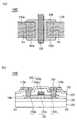
도 1의 (a)는, 반도체 장치의 구성의 일 형태인 트랜지스터(100)의 구조를 설명하는 상면도이며, 도 1의 (b)는, 도 1의 (a)에 A1-A2의 쇄선으로 나타낸 부위의 적층 구조를 설명하는 단면도다. 또한, 도 1의 (a)에서, 기판 및 절연층의 기재는 생략하고 있다.FIG. 1A is a top view illustrating the structure of a
도 1에 도시하는 트랜지스터(100)는, 기판(101) 위에 기초층(102)이 형성되고, 기초층(102) 위에 산화물 반도체층(103)이 형성되어 있다. 또한, 산화물 반도체층(103) 위에 게이트 절연층(104)이 형성되고, 게이트 절연층(104) 위에 게이트 전극(105)이 형성되어 있다. 또한, 게이트 전극(105) 위에 절연층(107)과 절연층(108)이 형성되고, 절연층(108) 위에, 소스 전극(110a) 및 드레인 전극(110b)이 형성되어 있다. 소스 전극(110a) 및 드레인 전극(110b)은, 게이트 절연층(104), 절연층(107) 및 절연층(108)에 형성된 컨택트 홀(109)을 통해 산화물 반도체층(103)에 전기적으로 접속되어 있다.In the
산화물 반도체층(103)은, 게이트 절연층(104)을 통해 게이트 전극(105)과 중첩하는 채널 형성 영역(103c)과, 소스 전극(110a)과 전기적으로 접속하는 소스 영역(103a)과, 드레인 전극(110b)과 전기적으로 접속하는 드레인 영역(103b)을 갖고 있다.The
또한, 게이트 전극(105)은, 게이트 절연층(104)에 접하는 게이트 전극(105a)과, 게이트 전극(105a)에 적층된 게이트 전극(105b)을 갖고 있다.The
또한, 도 1의 (a)에서는, 컨택트 홀(109)을, 소스 영역(103a) 및 드레인 영역(103b) 위에 각각 복수 형성하는 예를 나타내고 있지만, 소스 영역(103a) 및 드레인 영역(103b) 위에 각각 1개 형성하는 구성으로 해도 된다. 또한, 소스 전극(110a)과 소스 영역(103a)의 접촉 저항, 및 드레인 전극(110b)과 드레인 영역(103b)의 접촉 저항을 저감하기 위해서, 컨택트 홀(109)은 매우 크고 또한 컨택트 홀(109)의 수를 많게 하는 것이 바람직하다.In FIG. 1A, an example in which a plurality of contact holes 109 are formed on the
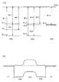
도 2에 도시하는 트랜지스터(140)는, 트랜지스터(100)의 구성 외에 게이트 전극(105)의 측면에 사이드 월(111)을 갖고, 산화물 반도체층(103)의 사이드 월(111)과 중첩하는 영역에, 저농도 영역(103d) 및 저농도 영역(103e)을 갖고 있다. 저농도 영역(103d)은 채널 형성 영역(103c)과 소스 영역(103a)의 사이에 형성되고, 저농도 영역(103e)은 채널 형성 영역(103c)과 드레인 영역(103b)의 사이에 형성되어 있다. 도 2의 (a)는, 트랜지스터(140)의 구성을 설명하는 상면도이며, 도 2의 (b)는, 도 2의 (a)에 B1-B2의 쇄선으로 나타낸 부위의 적층 구조를 설명하는 단면도다.The
저농도 영역(103d) 및 저농도 영역(103e)을 형성함으로써, 트랜지스터 특성의 열화나 단채널 효과에 의한 임계값 전압의 마이너스 시프트를 경감할 수 있다.By forming the
트랜지스터(100) 및 트랜지스터(140)는, 톱 게이트 구조의 트랜지스터의 일 형태다.The
다음으로, 도 1에 도시하는 트랜지스터(100)의 제작 방법에 대해서 도 3 및 도 4를 이용하여 설명한다. 또한, 도 3 및 도 4는, 도 1의 (a)의 A1-A2의 쇄선으로 나타낸 부위의 단면에 상당한다.Next, the manufacturing method of the
우선, 기판(101) 위에 기초층(102)을 50nm 이상 300nm 이하, 바람직하게는 100nm 이상 200nm 이하의 두께로 형성한다. 기판(101)은, 유리 기판, 세라믹 기판 외에, 본 제작 공정의 처리 온도에 견딜 수 있는 정도의 내열성을 갖는 플라스틱 기판 등을 이용할 수 있다. 또한, 기판에 투광성을 필요로 하지 않는 경우에는, 스테인레스 합금 등의 금속 기판의 표면에 절연층을 설치한 것을 이용해도 된다. 유리 기판으로는, 예를 들면, 바륨 붕규산염 유리, 알루미노 붕규산염 유리 혹은 알루미노 규산 유리 등의 무알카리 유리 기판을 이용하면 좋다. 그 외에, 석영 기판, 사파이어 기판 등을 이용할 수 있다. 또한, 실리콘이나 탄화 실리콘 등의 단결정 반도체 기판, 다결정 반도체 기판, 실리콘 게르마늄 등의 화합물 반도체 기판, SOI 기판 등을 적용하는 것도 가능하며, 이들 기판 위에 반도체 소자가 설치된 것을 기판(101)으로서 이용해도 된다.First, the
기초층(102)은, 질화 알루미늄, 산화 알루미늄, 질화산화 알루미늄, 산화질화 알루미늄, 질화 실리콘, 산화 실리콘, 질화산화 실리콘 또는 산화질화 실리콘에서 선택된 재료를, 단층으로 또는 적층해서 형성할 수 있으며, 기판(101)으로부터의 불순물 원소의 확산을 방지하는 기능을 갖는다. 또한, 본 명세서 중에서, 질화 산화물이란, 그 조성으로서 산소보다 질소의 함유량이 많은 것이며, 산화 질화물이란, 그 조성으로서 질소보다 산소의 함유량이 많은 것을 나타낸다. 또한, 각 원소의 함유량은, 예를 들면 러더퍼드 후방 산란법(RBS:Rutherford Backscattering Spectrometry) 등을 이용해서 측정할 수 있다.The
기초층(102)은, 스퍼터링법, CVD법, 도포법, 인쇄법 등을 적절히 이용할 수 있다. 본 실시 형태에서는, 기초층(102)으로서 질화 실리콘과 산화 실리콘의 적층을 이용한다. 구체적으로는, 기판(101) 위에 질화 실리콘을 50nm의 두께로 형성하고, 해당 질화 실리콘 위에 산화 실리콘을 150nm의 두께로 형성한다. 또한, 기초층(102) 중에 인(P)이나 붕소(B)가 도프되어 있어도 좋다.The
또한, 기초층(102)에, 염소, 불소 등의 할로겐 원소를 포함시킴으로써, 기판(101)으로부터의 불순물 원소의 확산을 방지하는 기능을 더욱 높일 수 있다. 기초층(102)에 포함시키는 할로겐 원소의 농도는, SIMS(2차 이온 질량 분석계)를 이용한 분석에 의해 얻어지는 농도 피크에 있어서, 1×10¹⁵/cm3 이상 1×10²⁰/cm3 이하로 하면 된다.In addition, by including halogen elements such as chlorine and fluorine in the
또한, 기초층(102)은, 가열에 의해 산소 방출되는 재료를 이용해도 된다. "가열에 의해 산소 방출되는"이란, TDS(Thermal Desorption Spectroscopy:승온 이탈 가스 분광법) 분석에서, 산소 원자로 환산한 산소의 방출량이 1.0×10¹⁸atoms/cm3 이상, 바람직하게는 3.0×10²⁰atoms/cm3 이상인 것을 말한다.In addition, the
여기서, TDS 분석에서, 산소 원자로 환산한 산소의 방출량의 측정 방법에 대해 이하에 설명한다.Here, the method of measuring the amount of released oxygen converted into oxygen atoms in the TDS analysis will be described below.
TDS 분석했을 때의 기체의 방출량은, 스펙트럼의 적분값에 비례한다. 이 때문에, 절연층의 스펙트럼의 적분값과 표준 시료의 기준값에 대한 비에 의해, 기체의 방출량을 계산할 수 있다. 표준 시료의 기준값이란, 소정의 원자를 포함하는 시료의 스펙트럼의 적분값에 대한 원자의 밀도의 비율이다.The amount of gas released during TDS analysis is proportional to the integral value of the spectrum. For this reason, the discharge | emission amount of gas can be calculated by ratio with respect to the integral value of the spectrum of an insulating layer, and the reference value of a standard sample. The reference value of the standard sample is the ratio of the density of atoms to the integrated value of the spectrum of the sample containing the predetermined atoms.
예를 들면, 표준 시료인 소정의 밀도의 수소를 포함하는 실리콘 웨이퍼의 TDS 분석 결과, 및 절연층의 TDS 분석 결과로부터, 절연층의 산소 분자의 방출량(NO2)은 수학식 1로 구할 수 있다. 여기서, TDS 분석에서 얻어지는 질량수 32로 검출되는 스펙트럼 모두가 산소 분자 유래라고 가정한다. 질량수 32인 것으로서 CH3OH가 있지만, 존재할 가능성이 낮은 것으로서 여기에서는 고려하지 않는다. 또한, 산소 원자의 동위체인 질량수 17의 산소 원자 및 질량수 18의 산소 원자를 포함하는 산소 분자에 대해서도, 자연계에서의 존재 비율이 극미량이기 때문에 고려하지 않는다.For example, from the TDS analysis result of the silicon wafer containing hydrogen of a predetermined density which is a standard sample, and the TDS analysis result of the insulating layer, the amount of oxygen molecules released from the insulating layer (NO2 ) can be obtained from
<수학식 1>&Quot; (1) "
NO2 = NH2/SH2×SO2×αNO2 = NH2 / SH2 × SO2 × α
NH2는, 표준 시료로부터 이탈한 수소 분자를 밀도로 환산한 값이다. SH2는, 표준 시료를 TDS 분석했을 때의 스펙트럼의 적분값이다. 여기서, 표준 시료의 기준값을 NH2/SH2라고 한다. SO2는, 절연층을 TDS 분석했을 때의 스펙트럼의 적분값이다. α는, TDS 분석에서의 스펙트럼 강도에 영향을 주는 계수다. 수학식 1의 상세에 관해서는, 일본 특허 공개 평 6-275697 공보를 참조한다. 또한, 상기 절연층의 산소의 방출량은, 전자과학 주식회사 제조의 승온 이탈 분석 장치 EMD-WA100OS/W를 이용하고, 표준 시료로서 1×10¹⁶atoms/cm3의 수소 원자를 포함하는 실리콘 웨이퍼를 이용해서 측정했다.NH2 is a value obtained by converting hydrogen molecules separated from a standard sample into density. SH2 is an integral value of the spectrum when the TDS analysis of the standard sample is performed. Here, the reference value of the standard sample is referred to as NH2 / SH2 .SO2 is an integral value of the spectrum when the insulating layer is analyzed by TDS. α is a coefficient that affects the spectral intensity in the TDS analysis. For the details of
또한, TDS 분석에서, 산소의 일부는 산소 원자로서 검출된다. 산소 분자와 산소 원자의 비율은, 산소 분자의 이온화율로부터 산출할 수 있다. 또한, 상술한 α는 산소 분자의 이온화율을 포함하기 때문에, 산소 분자의 방출량을 평가함으로써 산소 원자의 방출량에 대해서도 어림할 수 있다.In addition, in TDS analysis, part of the oxygen is detected as an oxygen atom. The ratio of oxygen molecules and oxygen atoms can be calculated from the ionization rate of the oxygen molecules. In addition, since alpha mentioned above contains the ionization rate of an oxygen molecule, the quantity of oxygen atoms can be estimated by evaluating the amount of oxygen molecules released.
또한, NO2는 산소 분자의 방출량이다. 절연층에서는, 산소 원자로 환산했을 때의 산소의 방출량은, 산소 분자의 방출량의 2배가 된다.In addition, NO2 is the amount of oxygen molecules released. In the insulating layer, the amount of oxygen released when converted into oxygen atoms is twice the amount of released oxygen molecules.
상기 구성에서, 가열에 의해 산소 방출되는 절연층은, 산소가 과잉인 산화 실리콘[SiOX(X>2)]이어도 된다. 산소가 과잉인 산화 실리콘[SiOX(X>2)]이란, 실리콘 원자수의 2배보다 많은 산소 원자를 단위 체적당 포함하는 것이다. 단위 체적당의 실리콘 원자수 및 산소 원자수는, 러더퍼드 후방 산란법에 의해 측정한 값이다.In the above configuration, the insulating layer released by oxygen by heating may be silicon oxide [SiOX (X> 2)] with excessive oxygen. The excess silicon oxide [SiOX (X> 2)] contains oxygen atoms per unit volume more than twice the number of silicon atoms. The number of silicon atoms and the number of oxygen atoms per unit volume are values measured by the Rutherford backscattering method.
기초층으로부터 산화물 반도체에 산소가 공급됨으로써, 기초층 및 산화물 반도체의 계면 준위를 저감할 수 있다. 그 결과, 트랜지스터의 동작 등에 기인해서 생길 수 있는 전하 등이, 상술한 기초층 및 산화물 반도체의 계면에 포획되는 것을 억제할 수가 있어, 전기 특성의 열화가 적은 트랜지스터를 얻을 수 있다.By supplying oxygen to the oxide semiconductor from the base layer, the interface levels of the base layer and the oxide semiconductor can be reduced. As a result, it is possible to suppress that charges, etc., which may be generated due to the operation of the transistor and the like, are trapped at the interface between the base layer and the oxide semiconductor described above, and a transistor with less deterioration in electrical characteristics can be obtained.
또한, 산화물 반도체의 산소 결손에 기인해서 전하가 생기는 경우가 있다. 일반적으로 산화물 반도체의 산소 결손은, 일부가 도너가 되어 캐리어인 전자를 발생시킨다. 그 결과, 트랜지스터의 임계값 전압이 마이너스 방향으로 시프트된다. 이러한 경향은 백 채널측에서 생기는 산소 결손에 있어서 현저하다. 또한, 본 명세서에서의 백 채널이란, 산화물 반도체에 있어서 기초층의 계면 근방을 가리킨다. 기초층으로부터 산화물 반도체에 산소가 충분히 방출됨으로써, 임계값 전압이 마이너스 방향으로 시프트하는 요인인 산화물 반도체의 산소 결손을 보충할 수 있다.In addition, charges may occur due to oxygen vacancies in the oxide semiconductor. In general, oxygen vacancies in the oxide semiconductor generate electrons which are carriers, a part of which is a donor. As a result, the threshold voltage of the transistor is shifted in the negative direction. This tendency is remarkable in oxygen deficiency occurring on the back channel side. In addition, the back channel in this specification refers to the interface vicinity of a base layer in an oxide semiconductor. By sufficiently releasing oxygen from the base layer to the oxide semiconductor, oxygen deficiency of the oxide semiconductor, which is a factor in which the threshold voltage shifts in the negative direction, can be compensated.
즉, 산화물 반도체에 산소 결손이 생기면, 기초층과 산화물 반도체의 계면에서의 전하의 포획을 억제하는 것이 곤란해지는 바, 기초층에, 가열에 의해 산소 방출되는 절연층을 설치함으로써, 산화물 반도체 및 기초층의 계면 준위 및 산화물 반도체의 산소 결손을 저감하여, 산화물 반도체 및 기초층의 계면에서의 전하 포획의 영향을 작게 할 수 있다.In other words, when oxygen vacancies occur in the oxide semiconductor, it becomes difficult to suppress charge trapping at the interface between the base layer and the oxide semiconductor. An oxide semiconductor and a foundation are formed in the base layer by providing an insulating layer that is released oxygen by heating. The interface level of the layer and the oxygen vacancies of the oxide semiconductor can be reduced, and the influence of charge trapping at the interface between the oxide semiconductor and the base layer can be reduced.
또한, 기초층(102)에는, 이 후 형성하는 산화물 반도체와 동종의 성분을 포함하는 절연 재료를 이용해도 된다. 기초층(102)을 서로 다른 층의 적층으로 하는 경우에는, 산화물 반도체에 접하는 층을 산화물 반도체와 동종의 성분을 포함하는 절연 재료로 하면 된다. 이러한 재료는 산화물 반도체와의 상성이 좋아, 이것을 기초층(102)에 이용함으로써, 산화물 반도체와의 계면의 상태를 양호하게 유지할 수 있기 때문이다. 여기서, "산화물 반도체와 동종의 성분"이란, 산화물 반도체의 구성 원소에서 선택되는 하나 또는 복수의 원소를 의미한다. 예를 들면, 산화물 반도체가 In-Ga-Zn계의 산화물 반도체 재료에 의해 구성되는 경우, 동종의 성분을 포함하는 절연 재료로는 산화 갈륨 등이 있다.In addition, you may use for the
다음으로, 기초층(102) 위에 산화물 반도체를 형성한다. 또한, 전처리로서, 산화물 반도체에 수소, 수산기 및 수분이 가능한 한 포함되지 않도록 하기 위해서, 성막 장치의 예비 가열실에서 기판(101)을 예비 가열하여, 기판(101)이나 기초층(102)에 흡착된 수소, 수분 등의 불순물을 이탈시켜 배기하는 것이 바람직하다. 또한, 예비 가열실에 설치하는 배기 수단은 크라이오 펌프가 바람직하다. 또한, 상기 예비 가열의 처리는 생략할 수도 있다. 또한 상기 예비 가열은, 기초층(102)의 성막 전에 기판(101)에도 마찬가지로 행해도 된다.Next, an oxide semiconductor is formed on the
산화물 반도체로는, 적어도 인듐(In) 혹은 아연(Zn)을 포함하는 것이 바람직하다. 특히 In과 Zn을 포함하는 것이 바람직하다. 또한, 해당 산화물 반도체를 이용한 트랜지스터의 전기 특성의 변동을 줄이기 위한 스테빌라이저로서, 그것들 외에 갈륨(Ga)을 갖는 것이 바람직하다. 또한, 스테빌라이저로서 주석(Sn)을 갖는 것이 바람직하다. 또한, 스테빌라이저로서 하프늄(Hf)을 갖는 것이 바람직하다. 또한, 스테빌라이저로서 알루미늄(Al)을 갖는 것이 바람직하다.It is preferable that an oxide semiconductor contains at least indium (In) or zinc (Zn). It is particularly preferable to include In and Zn. Moreover, as a stabilizer for reducing the fluctuation | variation of the electrical characteristics of the transistor using this oxide semiconductor, it is preferable to have gallium (Ga) besides them. Further, it is preferable to have tin (Sn) as a stabilizer. Further, it is preferable to have hafnium (Hf) as a stabilizer. Further, it is preferable to have aluminum (Al) as a stabilizer.
또한, 다른 스테빌라이저로서, 란타노이드인 란탄(La), 세륨(Ce), 프라세오디뮴(Pr), 네오디뮴(Nd), 사마륨(Sm), 유로퓸(Eu), 가돌리늄(Gd), 테르븀(Tb), 디스프로슘(Dy), 홀뮴(Ho), 에르븀(Er), 툴륨(Tm), 이테르븀(Yb), 루테튬(Lu) 중 어느 1종 혹은 복수 종을 가져도 좋다.In addition, as other stabilizers, lanthanides such as lanthanum (La), cerium (Ce), praseodymium (Pr), neodymium (Nd), samarium (Sm), europium (Eu), gadolinium (Gd), terbium (Tb), You may have any 1 type or multiple types of dysprosium (Dy), holmium (Ho), erbium (Er), thulium (Tm), ytterbium (Yb), and lutetium (Lu).
예를 들면, 산화물 반도체로서 산화 인듐, 산화 주석, 산화 아연, 2원계 금속의 산화물인 In-Zn계 산화물, Sn-Zn계 산화물, Al-Zn계 산화물, Zn-Mg계 산화물, Sn-Mg계 산화물, In-Mg계 산화물, In-Ga계 산화물, 3원계 금속의 산화물인 In-Ga-Zn계 산화물(IGZO라고도 표기함), In-Al-Zn계 산화물, In-Sn-Zn계 산화물, Sn-Ga-Zn계 산화물, Al-Ga-Zn계 산화물, Sn-Al-Zn계 산화물, In-Hf-Zn계 산화물, In-La-Zn계 산화물, In-Ce-Zn계 산화물, In-Pr-Zn계 산화물, In-Nd-Zn계 산화물, In-Sm-Zn계 산화물, In-Eu-Zn계 산화물, In-Gd-Zn계 산화물, In-Tb-Zn계 산화물, In-Dy-Zn계 산화물, In-Ho-Zn계 산화물, In-Er-Zn계 산화물, In-Tm-Zn계 산화물, In-Yb-Zn계 산화물, In-Lu-Zn계 산화물, 4원계 금속의 산화물인 In-Sn-Ga-Zn계 산화물, In-Hf-Ga-Zn계 산화물, In-Al-Ga-Zn계 산화물, In-Sn-Al-Zn계 산화물, In-Sn-Hf-Zn계 산화물, In-Hf-Al-Zn계 산화물을 이용할 수 있다.For example, indium oxide, tin oxide, zinc oxide, In-Zn oxide, Sn-Zn oxide, Al-Zn oxide, Zn-Mg oxide, Sn-Mg oxide as oxide semiconductors Oxides, In-Mg oxides, In-Ga oxides, In-Ga-Zn oxides (also referred to as IGZO), oxides of ternary metals, In-Al-Zn oxides, In-Sn-Zn oxides, Sn-Ga-Zn oxide, Al-Ga-Zn oxide, Sn-Al-Zn oxide, In-Hf-Zn oxide, In-La-Zn oxide, In-Ce-Zn oxide, In- Pr-Zn oxide, In-Nd-Zn oxide, In-Sm-Zn oxide, In-Eu-Zn oxide, In-Gd-Zn oxide, In-Tb-Zn oxide, In-Dy- Zn oxide, In-Ho-Zn oxide, In-Er-Zn oxide, In-Tm-Zn oxide, In-Yb-Zn oxide, In-Lu-Zn oxide, quaternary metal oxide In-Sn-Ga-Zn oxide, In-Hf-Ga-Zn oxide, In-Al-Ga-Zn oxide, In-Sn-Al-Zn oxide, In-Sn-Hf-Zn oxide, In-Hf-Al-Zn-based oxides can be used The.
산화물 반도체층은, 바람직하게는 In을 함유하는 산화물 반도체, 더욱 바람직하게는 In 및 Ga를 함유하는 산화물 반도체다.The oxide semiconductor layer is preferably an oxide semiconductor containing In, more preferably an oxide semiconductor containing In and Ga.
여기서, 예를 들면 In-Ga-Zn계 산화물이란, 인듐(In), 갈륨(Ga), 아연(Zn)을 갖는 산화물이라는 의미이며, In과 Ga와 Zn의 비율은 상관없다. 또한, In과 Ga와 Zn 이외의 금속 원소를 포함해도 된다.Here, for example, an In—Ga—Zn-based oxide means an oxide having indium (In), gallium (Ga), and zinc (Zn), and the ratio of In, Ga, and Zn does not matter. Moreover, metal elements other than In, Ga, and Zn may be included.
또한, 산화물 반도체층은, 화학식 InMO3(ZnO)m (m>0)으로 표기되는 박막을 이용할 수 있다. 여기서 M은, Sn, Zn, Ga, Al, Mn 및 Co에서 선택된 하나 또는 복수의 금속 원소를 나타낸다. 또한, 산화물 반도체로서, In3SnO5(ZnO)n (n>0)으로 표기되는 재료를 이용해도 된다.As the oxide semiconductor layer, a thin film represented by the formula InMO3 (ZnO)m (m> 0) can be used. M represents one or a plurality of metal elements selected from Sn, Zn, Ga, Al, Mn, and Co. As the oxide semiconductor, a material represented by In3 SnO5 (ZnO)n (n> 0) may be used.
예를 들면, In:Ga:Zn=1:1:1(=1/3:1/3:1/3) 혹은 In:Ga:Zn=2:2:1(=2/5:2/5:1/5)의 원자수비인 In-Ga-Zn계 산화물이나 그 조성 근방의 산화물을 이용할 수 있다. 혹은, In:Sn:Zn=1:1:1(=1/3:1/3:1/3), In:Sn:Zn=2:1:3(=1/3:1/6:1/2) 혹은 In:Sn:Zn=2:1:5(=1/4:1/8:5/8)의 원자수비인 In-Sn-Zn계 산화물이나 그 조성 근방의 산화물을 이용하면 좋다.For example, In: Ga: Zn = 1: 1: 1 (= 1/3: 1/3: 1/3) or In: Ga: Zn = 2: 2: 1 (= 2/5: 2/5 In-Ga-Zn-based oxides having an atomic ratio of: 1/5) and oxides in the vicinity of the composition can be used. Or In: Sn: Zn = 1: 1: 1 (= 1/3: 1/3: 1/3), In: Sn: Zn = 2: 1: 3 (= 1/3: 1/6: 1 / 2) or an In-Sn-Zn-based oxide having an atomic ratio of In: Sn: Zn = 2: 1: 5 (= 1/4: 1/8: 5/8) or an oxide near its composition may be used. .
그러나, 이들에 한정되지 않고, 필요로 하는 반도체 특성(이동도, 임계값, 격차 등)에 따라서 적절한 조성의 것을 이용하면 좋다. 또한, 필요로 하는 반도체 특성을 얻기 위해서, 캐리어 밀도나 불순물 농도, 결함 밀도, 금속 원소와 산소의 원자수비, 원자간 결합 거리, 밀도 등을 적절한 것으로 하는 것이 바람직하다.However, the present invention is not limited to these, and those having an appropriate composition may be used according to the semiconductor characteristics (mobility, threshold value, gap, etc.) required. Moreover, in order to acquire the required semiconductor characteristic, it is preferable to make carrier density, impurity concentration, defect density, atomic ratio of a metal element and oxygen, bond distance between atoms, density, etc. into an appropriate thing.
예를 들면, In-Sn-Zn계 산화물에서는 비교적 용이하게 높은 이동도가 얻어진다. 그러나, In-Ga-Zn계 산화물에서도, 벌크 내 결함 밀도를 저감함으로써 이동 도를 높일 수 있다.For example, in In—Sn—Zn-based oxides, high mobility can be obtained relatively easily. However, even in In—Ga—Zn-based oxides, mobility can be increased by reducing the defect density in the bulk.
또한, 예를 들면, In, Ga, Zn의 원자수비가 In:Ga:Zn=a:b:c (a+b+c=1)인 산화물의 조성이, 원자수비가 In:Ga:Zn=A:B:C (A+B+C=1)인 산화물의 조성의 근방이라는 것은, a, b, c가 (a-A)2+(b-B)2+(c-C)2≤r2를 만족하는 것을 말하며, r는, 예를 들면 0.05로 하면 된다. 다른 산화물에서도 마찬가지이다.For example, the composition of the oxide whose atomic ratio of In, Ga, and Zn is In: Ga: Zn = a: b: c (a + b + c = 1) has an atomic ratio of In: Ga: Zn = The vicinity of the composition of an oxide of A: B: C (A + B + C = 1) means that a, b, and c satisfy (aA)2 + (bB)2 + (cC)2 ≤ r2 . In other words, r may be, for example, 0.05. The same is true for other oxides.
산화물 반도체는 단결정이거나 비단결정이어도 좋다. 후자의 경우, 아몰퍼스이거나 다결정이어도 좋다. 또한, 아몰퍼스 중에 결정성을 갖는 부분을 포함하는 구조이거나 비아몰퍼스이어도 좋다.The oxide semiconductor may be single crystal or non-single crystal. In the latter case, amorphous or polycrystalline may be used. Moreover, the structure containing the part which has crystallinity in amorphous, or via-morphus may be sufficient.
아몰퍼스 상태의 산화물 반도체는, 비교적 용이하게 평탄한 표면을 얻을 수 있기 때문에, 이것을 이용해서 트랜지스터를 제작했을 때의 계면 산란을 저감할 수 있어, 비교적 용이하게 비교적 높은 이동도를 얻을 수 있다.Since the oxide semiconductor in an amorphous state can obtain a flat surface relatively easily, the interfacial scattering when a transistor is fabricated using this can be reduced, and relatively high mobility can be obtained relatively easily.
또한, 결정성을 갖는 산화물 반도체에서는, 보다 벌크 내 결함을 저감할 수 있으며, 표면의 평탄성을 높이면 아몰퍼스 상태의 산화물 반도체 이상의 이동도를 얻을 수 있다. 표면의 평탄성을 높이기 위해서는, 평탄한 표면 위에 산화물 반도체를 형성하는 것이 바람직하고, 구체적으로는 평균 면 거칠기(Ra)가 1nm 이하, 바람직하게는 0.3nm 이하, 보다 바람직하게는 0.1nm 이하의 표면 위에 형성하면 좋다. 또한, Ra는 원자간력 현미경(AFM:Atomic Force Microscope)으로 평가 가능하다.In addition, in the oxide semiconductor having crystallinity, defects in bulk can be further reduced, and the mobility of the oxide semiconductor in an amorphous state can be obtained by increasing the flatness of the surface. In order to increase the flatness of the surface, it is preferable to form an oxide semiconductor on the flat surface, and specifically, the average surface roughness Ra is formed on the surface of 1 nm or less, preferably 0.3 nm or less, more preferably 0.1 nm or less. Do it. Ra can also be evaluated by atomic force microscopy (AFM).
결정성을 갖는 산화물 반도체로는, CAAC-OS(C Axis Aligned Crystalline Oxide Semiconductor)가 바람직하다. CAAC-OS는, 완전한 단결정이 아니며 완전한 비정질도 아니다. CAAC-OS는, 비정질상에 결정부를 갖는 결정-비정질 혼상 구조의 산화물 반도체다. 또한, 해당 결정부는, 한 변이 100nm 미만의 입방체 내에 들어가는 크기인 경우가 많다. 또한, 투과형 전자 현미경(TEM:Transmission Electron Microscope)에 의한 관찰 상에서는, CAAC-OS에 포함되는 비정질부와 결정부의 경계는 명확하지 않다. 또한, TEM에 의해 CAAC-OS에는 입계(그레인 경계라고도 함)를 확인할 수 없다. 그 때문에, CAAC-OS는, 입계에 기인하는 전자 이동도의 저하가 억제된다.As the oxide semiconductor having crystallinity, CA Axis-C (C Axis Aligned Crystalline Oxide Semiconductor) is preferable. CAAC-OS is not a complete single crystal nor is it completely amorphous. CAAC-OS is an oxide semiconductor having a crystal-amorphous mixed phase structure having a crystal part in an amorphous phase. In addition, this crystal part is often the size which one side enters in a cube of less than 100 nm. In addition, on the observation by a transmission electron microscope (TEM), the boundary between the amorphous part and the crystal part included in the CAAC-OS is not clear. In addition, due to TEM, grain boundaries (also called grain boundaries) cannot be identified in CAAC-OS. Therefore, in CAAC-OS, the fall of the electron mobility resulting from a grain boundary is suppressed.
CAAC-OS에 포함되는 결정부는, c축이 CAAC-OS의 피 형성면의 법선 벡터 또는 표면의 법선 벡터에 평행한 방향으로 정렬되고, 또한 ab면에 수직인 방향으로부터 보아 삼각형상 또는 육각형상의 원자 배열을 가지며, c축에 수직인 방향으로부터 보아 금속원자가 층 형상 또는 금속 원자와 산소 원자가 층 형상으로 배열되어 있다. 또한, 서로 다른 결정부 사이에서 각각 a축 및 b축의 방향이 상이해도 좋다. 본 명세서에서, 간단히 수직이라고 기재하는 경우, 85°이상 95°이하의 범위도 포함되는 것으로 한다. 또한, 간단히 평행이라고 기재하는 경우, -5°이상 5°이하의 범위도 포함되는 것으로 한다.The crystal part included in CAAC-OS is a triangular or hexagonal atom whose c-axis is aligned in a direction parallel to the normal vector of the to-be-formed surface of the CAAC-OS or the normal vector of the surface, and also perpendicular to the ab plane. The metal atoms are arranged in a layered form or the metal atoms and oxygen atoms are arranged in a layer form as viewed from a direction perpendicular to the c axis. In addition, the directions of the a-axis and the b-axis may be different between the different crystal parts, respectively. In this specification, when simply described as vertical, the range of 85 degrees or more and 95 degrees or less shall also be included. In addition, when it describes simply as parallel, the range of -5 degrees or more and 5 degrees or less shall also be included.
또한, CAAC-OS에서, 결정부의 분포가 똑같지 않아도 좋다. 예를 들면, CAAC-OS의 형성 과정에서, 산화물 반도체막의 표면측에서 결정 성장시키는 경우, 피 형성면의 근방에 대해 표면의 근방에서는 결정부가 차지하는 비율이 높아지는 경우가 있다. 또한, CAAC-OS에 불순물을 첨가함으로써, 해당 불순물 첨가 영역에서 결정부가 비정질화하는 경우도 있다.In the CAAC-OS, the distribution of crystal parts may not be the same. For example, when crystal growth is carried out on the surface side of the oxide semiconductor film during the formation of the CAAC-OS, the ratio of the crystal portion in the vicinity of the surface to the vicinity of the surface to be formed may increase. In addition, by adding an impurity to the CAAC-OS, the crystal part may be amorphous in the impurity addition region.
CAAC-OS에 포함되는 결정부의 c축은, CAAC-OS의 피 형성면의 법선 벡터 또는 표면의 법선 벡터에 평행한 방향으로 정렬되기 때문에, CAAC-OS의 형상(피 형성면의 단면 형상 또는 표면의 단면 형상)에 따라서는 서로 상이한 방향을 향하는 경우가 있다. 또한, 결정부의 c축의 방향은, CAAC-OS가 형성되었을 때의 피 형성면의 법선 벡터 또는 표면의 법선 벡터에 평행한 방향이 된다. 결정부는, 성막함으로써, 또는 성막 후에 가열 처리 등의 결정화 처리를 행함으로써 형성된다.Since the c-axis of the crystal part included in the CAAC-OS is aligned in a direction parallel to the normal vector of the surface to be formed of CAAC-OS or the normal vector of the surface, the shape of the CAAC-OS (the cross-sectional shape of the surface to be formed or the surface of Depending on the cross-sectional shape), they may face different directions. The c-axis direction of the crystal part is a direction parallel to the normal vector of the surface to be formed or the normal vector of the surface when CAAC-OS is formed. The crystal part is formed by film formation or by performing crystallization treatment such as heat treatment after film formation.
CAAC-OS는, 그 조성 등에 따라서 도체이거나 반도체이거나 절연체이다. 또한, 그 조성 등에 따라서, 가시광에 대해 투명하거나 불투명하다. 또한, CAAC-OS의 일부는 질소로 치환되어도 좋다.CAAC-OS is a conductor, a semiconductor, or an insulator depending on the composition etc. Moreover, depending on the composition etc., it is transparent or opaque with respect to visible light. In addition, a part of CAAC-OS may be substituted with nitrogen.
CAAC-OS를 이용한 트랜지스터는, 가시광이나 자외광의 조사에 의한 전기 특성의 변동을 저감하는 것이 가능하다. 따라서, 해당 트랜지스터는 신뢰성이 높다.The transistor using CAAC-OS can reduce variations in electrical characteristics due to irradiation of visible light or ultraviolet light. Therefore, the transistor is highly reliable.
CAAC-OS에 포함되는 결정 구조의 일례에 대해서 도 15 내지 도 17을 이용해서 상세하게 설명한다. 또한, 특별히 언급이 없는 한, 도 15 내지 도 17은 상방향을 c축 방향으로 하고, c축 방향과 직교하는 면을 ab면이라고 한다. 또한, 간단히 상부 절반, 하부 절반이라고 하는 경우, ab면을 경계로 했을 경우의 상부 절반, 하부 절반을 말한다. 또한, 도 15에서, 원으로 둘러싸인 O는 4배위의 O를 나타내고, 2중원으로 둘러싸인 O는 3배위의 O를 나타낸다.An example of the crystal structure included in CAAC-OS will be described in detail with reference to FIGS. 15 to 17. In addition, unless there is particular notice, FIGS. 15-17 make an upper direction into a c-axis direction, and the surface orthogonal to a c-axis direction is called ab surface. In addition, the upper half and the lower half are simply referred to as the upper half and the lower half when the ab plane is the boundary. In Fig. 15, O surrounded by circles represents O in four coordination, and O surrounded by double circles represents O in three coordination.
도 15의 (a)에, 1개의 6배위의 In과, In에 근접한 6개의 4배위의 산소 원자(이하, 4배위의 O)를 갖는 구조를 나타낸다. 여기서는, 금속 원자가 1개에 대하여 근접한 산소 원자만 나타낸 구조를 소그룹이라고 부른다. 도 15의 (a)의 구조는, 팔면체 구조를 취하지만, 간단하게 하기 위하여 평면 구조로 나타내고 있다. 또한, 도 15의 (a)의 상부 절반 및 하부 절반에는 각각 3개씩 4배위의 O가 있다. 도 15의 (a)에 도시하는 소그룹은 전하가 0이다.In FIG.15 (a), the structure which has one 6th coordination In and six 4th coordination oxygen atoms (hereinafter, the 4th coordination O) close to In is shown. Here, the structure which shows only the oxygen atom which one metal atom adjoins with respect to one is called a small group. Although the structure of FIG. 15A has an octahedral structure, it is shown by planar structure for simplicity. In addition, in the upper half and the lower half of FIG. The small group shown in Fig. 15A has zero charge.
도 15의 (b)에, 1개의 5배위의 Ga와, Ga에 근접한 3개의 3배위의 산소 원자(이하, 3배위의 O)와, Ga에 근접한 2개의 4배위의 O를 갖는 구조를 나타낸다. 3배위의 O은 모두 ab면에 존재한다. 도 15의 (b)의 상부 절반 및 하부 절반에는 각각 1개씩 4배위의 O가 있다. 또한, In도 5배위를 취하기 때문에, 도 15의 (b)에 도시하는 구조를 취할 수 있다. 도 15의 (b)에 도시하는 소그룹은 전하가 0이다.FIG. 15B shows a structure having one 5-coordinate Ga, three tri-coordinate oxygen atoms close to Ga (hereinafter, 3-coordinate O), and two 4-coordinate O close to Ga. . All three coordination O is on the ab plane. In the upper half and the lower half of FIG. Since In also takes 5 coordination, the structure shown in Fig. 15B can be taken. The small group shown in Fig. 15B has zero charge.
도 15의 (c)에, 1개의 4배위의 Zn과, Zn에 근접한 4개의 4배위의 O를 갖는 구조를 나타낸다. 도 15의 (c) 상부 절반에는 1개의 4배위의 O가 있고, 하부 절반에는 3개의 4배위의 O가 있다. 또는, 도 15의 (c)의 상부 절반에 3개의 4배위의 O가 있고, 하부 절반에 1개의 4배위의 O가 있어도 좋다. 도 15의 (c)에 도시하는 소그룹은 전하가 0이다.15 (c) shows a structure having one quadrant of Zn and four quadrants of O close to Zn. In FIG. 15 (c), there is one quadrant of O in the upper half, and there are three quarters of O in the lower half. Alternatively, there may be three quadrupeds of O in the upper half of FIG. 15C and one quadrant of O in the lower half. The small group shown in Fig. 15C has zero charge.
도 15의 (d)에, 1개의 6배위의 Sn과, Sn에 근접한 6개의 4배위의 O를 갖는 구조를 나타낸다. 도 15의 (d)의 상부 절반에는 3개의 4배위의 O가 있고, 하부 절반에는 3개의 4배위의 O가 있다. 도 15의 (d)에 도시하는 소그룹은 전하가 +1이 된다.15 (d) shows a structure having one six coordinating Sn and six four coordinating O close to Sn. In the upper half of FIG. 15D, there are three quadrant O's, and the lower half has three quadrant O's. In the small group shown in Fig. 15D, the charge becomes +1.
도 15의 (e)에, 2개의 Zn을 포함하는 소그룹을 나타낸다. 도 15의 (e)의 상부 절반에는 1개의 4배위의 O가 있고, 하부 절반에는 1개의 4배위의 O가 있다. 도 15의 (e)에 도시하는 소그룹은 전하가 -1이 된다.In Fig. 15E, a small group containing two Zn is shown. In the upper half of FIG. 15E, there is one quadrant of O, and in the lower half there is one quadrant of O. In the small group shown in Fig. 15E, the charge becomes -1.
여기에서는, 복수의 소그룹의 집합체를 중 그룹이라고 하고, 복수 중에서 그룹의 집합체를 대그룹(유닛 셀이라고도 함)이라고 한다.Here, the aggregate of a plurality of small groups is called a middle group, and the aggregate of groups among the plurality is called a large group (also called a unit cell).
여기서, 이들 소그룹끼리 결합하는 규칙에 대해서 설명한다. 도 15의 (a)에 도시하는 6배위의 In의 상부 절반의 3개의 O는, 하방향으로 각각 3개의 근접 In을 가지며, 하부 절반의 3개의 O는, 상방향으로 각각 3개의 근접 In을 갖는다. 도 15의 (b)에 도시하는 5배위의 Ga의 상부 절반의 1개의 O는, 하방향으로 1개의 근접 Ga를 갖고, 하부 절반의 1개의 O는, 상방향으로 1개의 근접 Ga를 갖는다. 도 15의 (c)에 도시하는 4배위의 Zn 상부 절반의 1개의 O는, 하방향으로 1개의 근접 Zn을 갖고, 하부 절반의 3개의 O는, 상방향으로 각각 3개의 근접 Zn을 갖는다. 이와 같이, 금속 원자의 상방향의 4배위의 O의 수와, 그 O의 하방향에 있는 근접 금속 원자의 수는 동일하며, 마찬가지로 금속 원자 하방향의 4배위의 O의 수와, 그 O의 상방향에 있는 근접 금속 원자의 수는 동일하다. O는 4배위므로, 하방향에 있는 근접 금속 원자의 수와 상방향에 있는 근접 금속 원자의 수의 합은 4가 된다. 따라서, 금속 원자의 상방향에 있는 4배위의 O의 수와, 다른 금속 원자의 하방향에 있는 4배위의 O의 수의 합이 4개일 때, 금속 원자를 갖는 2종의 소그룹끼리는 결합할 수 있다. 예를 들면, 6배위의 금속 원자(In 또는 Sn)가 하부 절반의 4배위의 O를 사이에 두고 결합하는 경우, 4배위의 O가 3개이기 때문에, 5배위의 금속 원자(Ga 또는 In) 또는 4배위의 금속 원자(Zn) 중 어느 하나와 결합하게 된다.Here, the rule which combines these small groups is demonstrated. Three O's in the upper half of In coordination in 6 shown in Fig. 15A have three proximal In's in the downward direction, and three O's in the lower half's three O's in the upper direction. Have One O of the upper half of Ga of 5th coordination shown in FIG. 15B has one proximity Ga in the downward direction, and one O of the lower half has one proximity Ga in the upward direction. One O of the upper half of Zn in the 4th coordination shown in FIG. 15C has one adjacent Zn in the downward direction, and three O of the lower half has three adjacent Zn in the upward direction. Thus, the number of O coordination in the upper direction of the metal atom and the number of adjacent metal atoms in the downward direction of the O are the same, and the number of O in coordination of the metal atom in the downward direction of the metal atom is the same, and The number of adjacent metal atoms in the upward direction is the same. Since O is fourfold, the sum of the number of adjacent metal atoms in the downward direction and the number of adjacent metal atoms in the upward direction is four. Therefore, when the sum of the number of 4 coordination O in the upper direction of a metal atom and the number of 4 coordination O in the downward direction of another metal atom is four, two small groups which have a metal atom can combine together. have. For example, when a metal atom of six coordination (In or Sn) is bonded through the O in the lower half of the four coordination, there are three O coordination of three, so the metal atom of five coordination (Ga or In) Or a combination of any one of four coordinating metal atoms (Zn).
이들 배위수를 갖는 금속 원자는, c축 방향에서 4배위의 O를 사이에 두고 결합한다. 또한, 그 외에도 층 구조의 합계 전하가 0이 되도록 복수의 소그룹이 결합해서 중그룹을 구성한다.The metal atom which has these coordination number couple | bonds with O of 4 coordination in c-axis direction. In addition, a plurality of small groups are combined to form a middle group so that the total charge of the layer structure becomes zero.
도 16의 (a)에, In-Sn-Zn계 산화물의 층 구조를 구성하는 중그룹의 모델도를 나타낸다. 도 16의 (b)에, 3개의 중그룹으로 구성되는 대그룹을 나타낸다. 또한, 도 16의 (c)는, 도 16의 (b)의 층 구조를 c축 방향으로부터 관찰했을 경우의 원자 배열을 나타낸다.FIG. 16A shows a model diagram of a middle group constituting a layer structure of an In—Sn—Zn-based oxide. In Fig. 16B, a large group composed of three heavy groups is shown. 16C shows the atomic arrangement when the layer structure of FIG. 16B is observed from the c-axis direction.
도 16의 (a)에서는, 간단하게 하기 위해 3배위의 O는 생략하고, 4배위의 O는 개수만을 나타내고, 예를 들면, Sn 상부 절반 및 하부 절반에는 각각 3개씩 4배위의 O가 있는 것을 둥근 원의 3으로서 나타내고 있다. 마찬가지로, 도 16의 (a)에서, In 상부 절반 및 하부 절반에는 각각 1개씩 4배위의 O가 있으며, 둥근 원의 1로서 나타내고 있다. 또한 마찬가지로, 도 16의 (a)에서, 하부 절반에는 1개의 4배위의 O가 있고, 상부 절반에는 3개의 4배위의 O가 있는 Zn과, 상부 절반에는 1개의 4배위의 O가 있고, 하부 절반에는 3개의 4배위의 O가 있는 Zn을 나타내고 있다.In Fig. 16A, for the sake of simplicity, O in the third coordination is omitted, and O in the fourth coordination represents only the number. For example, there are three coordination O in the upper half and the lower half of Sn, respectively. It is shown as 3 of a round circle. Similarly, in Fig. 16A, the upper half and the lower half of In each have four coordinations of O, one of which is indicated as one of the round circles. Similarly, in Fig. 16A, there is one quadrant of O in the lower half, three quadrants of O in the upper half, and one quadrant of O in the upper half, and the lower half. Half shows Zn with three quadruple O's.
도 16의 (a)에서, In-Sn-Zn계 산화물의 층 구조를 구성하는 중그룹은, 위에서부터 순서대로 4배위의 O가 3개씩 상부 절반 및 하부 절반에 있는 Sn이, 4배위의 O가 1개씩 상부 절반 및 하부 절반에 있는 In과 결합하고, 그 In이, 상부 절반에 3개의 4배위의 O가 있는 Zn과 결합하고, 그 Zn의 하부 절반의 1개의 4배위의 O를 사이에 두고 4배위의 O가 3개씩 상부 절반 및 하부 절반에 있는 In과 결합하고, 그 In이, 상부 절반에 1개의 4배위의 O가 있는 Zn 2개로 이루어지는 소그룹과 결합하고, 이 소그룹 아래 절반의 1개의 4배위의 O를 사이에 두고 4배위의 O가 3개씩 상부 절반 및 하부 절반에 있는 Sn과 결합하고 있는 구성이다. 이 중그룹이 복수 결합해서 대그룹을 구성한다.In (a) of FIG. 16, the middle group constituting the layer structure of the In—Sn—Zn-based oxide includes Sn in the upper half and the lower half of three O coordinations three from the top in order. Is bonded one by one to In in the upper half and the lower half, and that In binds to Zn with three quarter-order O in the upper half, and one quadrant O in the lower half of the Zn Three O coordination O is combined with In in the upper half and the lower half, and the In is combined with two small groups consisting of two Zn with one 4-coordinate O in the upper half, and one half of the lower half of this subgroup. The four coordination O is interposed between three dogs with three coordinations of O and the Sn in the upper half and the lower half. Multiple of these middle groups combine to form a large group.
여기서, 3배위의 O 및 4배위의 O의 경우, 결합 1개당 전하는 각각 -0.667, -0.5로 생각할 수 있다. 예를 들면, In(6배위 또는 5배위), Zn(4배위), Sn(5배위 또는 6배위)의 전하는, 각각 +3, +2, +4이다. 따라서, Sn을 포함하는 소그룹은 전하가 +1이 된다. 그 때문에, Sn을 포함하는 층 구조를 형성하기 위해서는, 전하 +1을 없애는 전하 -1이 필요하다. 전하 -1을 취하는 구조로서, 도 15의 (e)에 도시한 바와 같이, 2개의 Zn을 포함하는 소그룹을 들 수 있다. 예를 들면, Sn을 포함하는 소그룹이 1개에 대하여 2개의 Zn을 포함하는 소그룹이 1개 있으면, 전하가 없어지기 때문에, 층 구조의 합계의 전하를 0으로 할 수 있다.Here, in the case of O in the third coordination and O in the fourth coordination, the charges per bond can be considered as -0.667 and -0.5, respectively. For example, the electric charges of In (6 coordination or 5 coordination), Zn (4 coordination) and Sn (5 coordination or 6 coordination) are +3, +2 and +4, respectively. Thus, a small group containing Sn has a charge of +1. Therefore, in order to form the layer structure containing Sn, the electric charge -1 which removes electric charge +1 is needed. As a structure which takes charge -1, as shown in FIG.15 (e), the small group containing two Zn is mentioned. For example, if there is one small group containing two Zns for one small group containing Sn, the charges are lost, so that the total charge of the layer structure can be zero.
구체적으로는, 도 16의 (b)에 도시한 대그룹이 반복됨으로써, In-Sn-Zn계 산화물의 결정(In2SnZn3O8)을 얻을 수 있다. 또한, 얻어지는 In-Sn-Zn계 산화물의 층 구조는, In2SnZn2O7(ZnO)m (m은 0 또는 자연수)으로 하는 조성식으로 나타낼 수 있다.Specifically, by repeating the large group shown in FIG. 16B, a crystal (In2 SnZn3 O8 ) of an In—Sn—Zn-based oxide can be obtained. Further, the layer structure of the In-SnZn-based oxide isobtained, In 2 SnZn 2 O 7 ( ZnO) m can be expressed by the composition formula as (m is 0 or a natural number).
또한, 그 외에도, 4원계 금속의 산화물인 In-Sn-Ga-Zn계 산화물이나, 3원계 금속의 산화물인 In-Ga-Zn계 산화물(IGZO라고도 표기함.), In-Al-Zn계 산화물, Sn-Ga-Zn계 산화물, Al-Ga-Zn계 산화물, Sn-Al-Zn계 산화물이나, In-Hf-Zn계 산화물, In-La-Zn계 산화물, In-Ce-Zn계 산화물, In-Pr-Zn계 산화물, In-Nd-Zn계 산화물, In-Sm-Zn계 산화물, In-Eu-Zn계 산화물, In-Gd-Zn계 산화물, In-Tb-Zn계 산화물, In-Dy-Zn계 산화물, In-Ho-Zn계 산화물, In-Er-Zn계 산화물, In-Tm-Zn계 산화물, In-Yb-Zn계 산화물, In-Lu-Zn계 산화물이나, 2원계 금속의 산화물인 In-Zn계 산화물, Sn-Zn계 산화물, Al-Zn계 산화물, Zn-Mg계 산화물, Sn-Mg계 산화물, In-Mg계 산화물이나, In-Ga계 산화물 등을 이용한 경우도 마찬가지이다.In addition, In-Sn-Ga-Zn oxides, which are oxides of quaternary metals, In-Ga-Zn oxides (also referred to as IGZO), which are oxides of ternary metals, and In-Al-Zn oxides , Sn-Ga-Zn oxide, Al-Ga-Zn oxide, Sn-Al-Zn oxide, In-Hf-Zn oxide, In-La-Zn oxide, In-Ce-Zn oxide, In-Pr-Zn oxide, In-Nd-Zn oxide, In-Sm-Zn oxide, In-Eu-Zn oxide, In-Gd-Zn oxide, In-Tb-Zn oxide, In- Dy-Zn oxide, In-Ho-Zn oxide, In-Er-Zn oxide, In-Tm-Zn oxide, In-Yb-Zn oxide, In-Lu-Zn oxide, binary metal In-Zn oxides, Sn-Zn oxides, Al-Zn oxides, Zn-Mg oxides, Sn-Mg oxides, In-Mg oxides, In-Ga oxides, etc. It is the same.
예를 들면, 도 17의 (a)에, In-Ga-Zn계 산화물의 층 구조를 구성하는 중그룹의 모델도를 나타낸다.For example, FIG. 17A shows a model diagram of a middle group constituting a layer structure of an In—Ga—Zn-based oxide.
도 17의 (a)에서, In-Ga-Zn계 산화물의 층 구조를 구성하는 중그룹은, 위에서부터 순서대로 4배위의 O가 3개씩 상부 절반 및 하부 절반에 있는 In이, 4배위의 O가 1개 상부 절반에 있는 Zn과 결합하고, 그 Zn의 하부 절반의 3개의 4배위의 O를 사이에 두고, 4배위의 O가 1개씩 상부 절반 및 하부 절반에 있는 Ga와 결합하고, 그 Ga의 하부 절반의 1개의 4배위의 O를 사이에 두고, 4배위의 O가 3개씩 상부 절반 및 하부 절반에 있는 In과 결합하고 있는 구성이다. 이 중그룹이 복수 결합해서 대그룹을 구성한다.In (a) of FIG. 17, the middle group constituting the layer structure of the In—Ga—Zn-based oxide includes In, in which the O in the upper half and the lower half are three in four coordination O in order from the top, and the O in four coordination. Combines with Zn in one upper half, with three quadrant O coordination of the lower half of the Zn, and four coordination O one with Ga in the upper half and lower half, and the Ga The four coordination O's are interposed between three of the four coordination O's in the upper half and the lower half. Multiple of these middle groups combine to form a large group.
도 17의 (b)에 3개의 중그룹으로 구성되는 대그룹을 나타낸다. 또한, 도 17의 (c)은, 도 17의 (b)의 층 구조를 c축 방향으로부터 관찰한 경우의 원자 배열을 나타내고 있다.17B shows a large group composed of three heavy groups. 17C shows the atomic arrangement when the layer structure of FIG. 17B is observed from the c-axis direction.
여기서, In(6배위 또는 5배위), Zn(4배위), Ga(5배위)의 전하는, 각각 +3, +2, +3이기 때문에, In, Zn 및 Ga 중 어느 하나를 포함하는 소그룹은 전하가 0이 된다. 그 때문에, 이들 소그룹의 조합이라면 중그룹의 합계 전하는 항상 0이 된다.Here, since the charges of In (6 or 5 coordination), Zn (4 coordination), and Ga (5 coordination) are +3, +2, and +3, respectively, the small group containing any one of In, Zn, and Ga is The charge is zero. Therefore, in the combination of these small groups, the total charge of the medium group is always zero.
또한, In-Ga-Zn계 산화물의 층 구조를 구성하는 중그룹은, 도 17의 (a)에 도시한 중그룹에 한정되지 않고, In, Ga, Zn의 배열이 서로 다른 중그룹을 조합한 대그룹도 취할 수 있다.In addition, the middle group constituting the layer structure of the In—Ga—Zn-based oxide is not limited to the middle group shown in Fig. 17A, and a combination of heavy groups having different arrangements of In, Ga, and Zn is provided. Large groups can also be taken.
구체적으로는, 도 17의 (b)에 도시한 대그룹이 반복됨으로써, In-Ga-Zn계 산화물의 결정을 얻을 수 있다. 또한, 얻어지는 In-Ga-Zn계 산화물의 층 구조는, InGaO3(ZnO)n (n은 자연수)으로 하는 조성식으로 나타낼 수 있다.Specifically, by repeating the large group shown in FIG. 17B, a crystal of an In—Ga—Zn-based oxide can be obtained. In addition, In-Ga-Zn-based layer structure of the oxide is obtained, InGaO3 (ZnO)n can be represented by the composition formula as (n is a natural number).
n=1(InGaZnO4)인 경우에는, 예를 들면, 도 18의 (a)에 도시하는 결정 구조를 취할 수 있다. 또한, 도 18의 (a)에 도시하는 결정 구조에 있어서, 도 15의 (b)에서 설명한 바와 같이 Ga 및 In은 5배위를 취하기 때문에, Ga가 In으로 치환된 구조도 취할 수 있다.In the case of n = 1 (InGaZnO4 ), for example, the crystal structure shown in Fig. 18A can be taken. In addition, in the crystal structure shown in Fig. 18A, as shown in Fig. 15B, Ga and In take five coordination, so that Ga may be substituted with In.
또한, n=2(InGaZn2O5)인 경우에는, 예를 들면, 도 18의 (b)에 도시하는 결정 구조를 취할 수 있다. 또한, 도 18의 (b)에 도시하는 결정 구조에 있어서, 도 15의 (b)에서 설명한 바와 같이 Ga 및 In은 5배위를 취하기 때문에, Ga가 In으로 치환된 구조도 취할 수 있다.In addition, in the case of n = 2 (InGaZn2 O5 ), for example, the crystal structure shown in Fig. 18B can be taken. In addition, in the crystal structure shown in Fig. 18B, as shown in Fig. 15B, Ga and In take five coordination, so that Ga may be substituted with In.
본 실시 형태에서는, 우선 기초층(102) 위에 스퍼터링법에 의해 1nm 이상 10nm 이하의 제1 산화물 반도체를 형성한다. 제1 산화물 반도체를 형성할 때의 기판 온도는 200℃ 이상 400℃ 이하로 한다.In this embodiment, first, a first oxide semiconductor of 1 nm or more and 10 nm or less is formed on the
여기서, 산화물 반도체를 형성하는 스퍼터링 장치에 대해서 이하에 상세를 설명한다.Here, the sputtering apparatus which forms an oxide semiconductor is explained in full detail below.
산화물 반도체를 형성하는 성막실은, 리크 레이트를 1×10⁻¹⁰Pa?m3/초 이하로 하는 것이 바람직하고, 그에 따라 스퍼터링법에 의해 성막할 때, 막 내로의 불순물의 혼입을 저감할 수 있다.In the film formation chamber forming the oxide semiconductor, the leak rate is preferably 1 × 10⁻¹⁰ Pa · m3 / sec or less, and accordingly, when the film is formed by the sputtering method, the incorporation of impurities into the film can be reduced. .
리크 레이트를 낮게 하기 위해서는, 외부 리크뿐만 아니라 내부 리크를 저감할 필요가 있다. 외부 리크란, 미소한 구멍이나 시일 불량 등에 의해 진공계의 외부에서부터 기체가 유입하는 것이다. 내부 리크란, 진공계 내의 밸브 등의 구획으로부터의 누설이나 내부 부재로부터의 방출 가스에 기인한다. 리크 레이트를 1×10⁻¹⁰Pa?m3/초 이하로 하기 위해서는, 외부 리크 및 내부 리크의 양면에서 대책을 취할 필요가 있다.In order to lower the leak rate, it is necessary to reduce not only the external leak but also the internal leak. An external leak is a gas which flows in from the outside of a vacuum system by a micropore or a seal defect. Internal leaks are due to leakage from compartments such as valves in a vacuum system or discharge gas from internal members. In order to set the leak rate to 1 × 10⁻¹⁰ Pa · m3 / sec or less, it is necessary to take countermeasures on both of the external leak and the internal leak.
외부 리크를 줄이기 위해서는, 성막실의 개폐 부분은 메탈 가스켓으로 시일 하면 좋다. 메탈 가스켓은, 불화철, 산화 알루미늄 또는 산화 크롬에 의해 피복된 금속 재료를 이용하면 바람직하다. 메탈 가스켓은 O링과 비교해서 밀착성이 높아 외부 리크를 저감할 수 있다. 또한, 불화철, 산화 알루미늄, 산화 크롬 등의 부동태에 의해 피복된 금속 재료를 이용함으로써, 메탈 가스켓으로부터 발생하는 수소를 포함하는 방출 가스가 억제되어, 내부 리크도 저감할 수 있다.In order to reduce external leakage, the opening and closing portion of the deposition chamber may be sealed with a metal gasket. It is preferable to use a metal material coated with iron fluoride, aluminum oxide or chromium oxide as the metal gasket. Metal gaskets have high adhesion compared to O-rings and can reduce external leakage. In addition, by using a metal material coated by a passivation such as iron fluoride, aluminum oxide, and chromium oxide, the release gas containing hydrogen generated from the metal gasket can be suppressed, and the internal leak can also be reduced.
성막실의 내벽을 구성하는 부재로서, 수소를 포함하는 방출 가스가 적은 알루미늄, 크롬, 티타늄, 지르코늄, 니켈 또는 바나듐을 이용한다. 또한, 상술한 재료를 철, 크롬 및 니켈 등을 포함하는 합금 재료에 피복해서 이용해도 된다. 철, 크롬 및 니켈 등을 포함하는 합금 재료는 강성이 있으며, 열에 강하고, 또한 가공에 적합하다. 여기서, 표면적을 작게 하기 위해서 부재의 표면 요철을 연마 등에 의해 저감시켜 두면, 방출 가스를 저감할 수 있다. 혹은, 상술한 성막 장치의 부재를 불화철, 산화 알루미늄, 산화 크롬 등의 부동태로 피복해도 좋다.As a member constituting the inner wall of the film formation chamber, aluminum, chromium, titanium, zirconium, nickel or vanadium with a small amount of emission gas containing hydrogen is used. Moreover, you may coat | cover and use the material mentioned above on the alloy material containing iron, chromium, nickel, etc. Alloy materials including iron, chromium, nickel and the like are rigid, heat resistant, and suitable for processing. Here, when the surface unevenness of the member is reduced by polishing or the like in order to reduce the surface area, the emitted gas can be reduced. Or you may coat | cover the member of the film-forming apparatus mentioned above with the passivation type, such as iron fluoride, aluminum oxide, and chromium oxide.
또한, 스퍼터 가스를 성막실에 도입하기 직전에, 스퍼터 가스의 정제기를 설치하는 것이 바람직하다. 이때, 정제기로부터 성막실까지의 배관의 길이를 5m 이하, 바람직하게는 1m 이하로 한다. 배관의 길이를 5m 이하 또는 1m 이하로 함으로써, 배관으로부터의 방출 가스의 영향을 길이에 따라서 저감할 수 있다.Moreover, it is preferable to provide the refiner of sputter gas just before introducing a sputter gas into a film-forming chamber. At this time, the length of the pipe from the refiner to the film forming chamber is 5 m or less, preferably 1 m or less. By setting the length of the pipe to 5 m or less or 1 m or less, the influence of the discharged gas from the pipe can be reduced along the length.
성막실의 배기는, 드라이 펌프 등의 러핑 펌프와, 스퍼터 이온 펌프, 터보 분자 펌프 및 크라이오 펌프 등의 고진공 펌프를 적절히 조합해서 행하면 좋다. 또한, 성막실 내의 잔류 수분을 제거하기 위해서는, 흡착형의 진공 펌프, 예를 들면 크라이오 펌프, 이온 펌프, 티탄 서블리메이션 펌프를 이용하는 것이 바람직하다. 터보 분자 펌프는 큰 사이즈의 분자의 배기가 우수한 한편, 수소나 물의 배기 능력이 낮다. 따라서, 물의 배기 능력이 높은 크라이오 펌프 및 수소의 배기 능력이 높은 스퍼터 이온 펌프를 조합하는 것이 유효하다. 또한, 터보 분자 펌프에 콜드 트랩을 부가한 것이어도 된다. 크라이오 펌프 등의 흡착형의 진공 펌프를 이용해서 배기한 성막실은, 예를 들면 수소원자, 물(H2O) 등 수소 원자를 포함하는 화합물(보다 바람직하게는 탄소 원자를 포함하는 화합물도) 등이 배기되기 때문에, 해당 성막실에서 성막한 산화물 반도체층에 포함되는 불순물의 농도를 저감할 수 있다.The film formation chamber may be exhausted by combining a rough pump such as a dry pump and a high vacuum pump such as a sputter ion pump, a turbo molecular pump, and a cryopump. In addition, in order to remove the residual moisture in the film formation chamber, it is preferable to use an adsorption type vacuum pump, for example, a cryopump, an ion pump, a titanium servation pump. The turbomolecular pump is excellent in exhausting large-sized molecules while having low capacity for exhausting hydrogen or water. Therefore, it is effective to combine a cryopump having a high water exhaust capacity and a sputter ion pump having a high hydrogen exhaust capacity. In addition, a cold trap may be added to the turbomolecular pump. The film formation chamber evacuated using an adsorption type vacuum pump such as a cryo pump is, for example, a compound containing a hydrogen atom such as a hydrogen atom and water (H2 O) (more preferably, a compound containing a carbon atom)) Since the gas is exhausted, the concentration of impurities contained in the oxide semiconductor layer formed in the film formation chamber can be reduced.
성막실의 내측에 존재하는 흡착물은, 내벽에 흡착되어 있기 때문에 성막실의 압력에 영향을 주지 않지만, 성막실을 배기했을 때의 가스 방출의 원인이 된다. 그 때문에, 리크 레이트와 배기 속도에 상관은 없지만, 배기 능력이 높은 펌프를 이용하여 성막실에 존재하는 흡착물을 가능한 한 이탈시켜 미리 배기해 두는 것이 중요하다. 또한, 흡착물의 이탈을 촉진시키기 위해서 성막실을 베이킹해도 좋다. 베이킹함으로써 흡착물의 이탈 속도를 10배 정도 크게 할 수 있다. 베이킹은 100℃ 이상 450℃ 이하로 행하면 좋다. 이때, 불활성 가스를 첨가하면서 흡착물의 제거를 행하면, 배기하는 것 만으로는 이탈시키기 어려운 물 등의 이탈 속도를 더욱 크게 할 수 있다.Since the adsorbate present inside the film formation chamber is adsorbed on the inner wall, it does not affect the pressure in the film formation chamber, but it is the cause of gas release when the film formation chamber is exhausted. Therefore, regardless of the leak rate and the exhaust speed, it is important to evacuate the adsorbate present in the deposition chamber as far as possible by using a pump having a high exhaust capacity and evacuate it in advance. Moreover, you may bake the film-forming chamber in order to accelerate | release the adsorbate. By baking, the removal rate of an adsorbate can be made about 10 times larger. Baking may be performed at 100 ° C or higher and 450 ° C or lower. At this time, if the adsorbate is removed while adding an inert gas, the release rate of water or the like that is difficult to be removed simply by evacuation can be further increased.
스퍼터링법에 있어서, 플라즈마를 발생시키기 위한 전원 장치는, RF 전원 장치, AC 전원 장치, DC 전원 장치 등을 적절히 이용할 수 있다.In the sputtering method, an RF power supply device, an AC power supply device, a DC power supply device, or the like can be suitably used as a power supply device for generating plasma.
산화물 반도체로서 In-Ga-Zn계 산화물 재료를 스퍼터링법으로 형성하기 위한 In-Ga-Zn계 산화물 타깃은, 예를 들면 In2O3:Ga2O3:ZnO=1:1:1 [mol수 비]의 조성비를 갖는 타깃을 이용할 수 있다. 또한, In2O3:Ga2O3:ZnO=1:1:2 [mol수 비]의 조성비를 갖는 타깃, 또는 In2O3:Ga2O3:ZnO=1:1:4 [mol수 비]의 조성비를 갖는 타깃, In2O3:Ga2O3:ZnO=2:1:8 [mol수 비]의 조성비를 갖는 타깃을 이용할 수도 있다. 또한, 원자수 비가 In:Ga:Zn=1:1:1, 4:2:3, 3:1:2, 1:1:2, 2:1:3 또는 3:1:4로 나타내지는 In-Ga-Zn계 산화물 타깃을 이용할 수 있다. 상술한 원자수 비를 갖는 In-Ga-Zn계 산화물 타깃을 이용해서 산화물 반도체를 형성함으로써, 다결정 또는 CAAC-OS가 형성되기 쉬워진다.An In—Ga—Zn oxide target for forming an In—Ga—Zn oxide material as an oxide semiconductor by sputtering may be, for example, In2 O3 : Ga2 O3 : ZnO = 1: 1: 1 [mol A target having a composition ratio of water ratio] can be used. In addition, a target having a composition ratio of In2 O3 : Ga2 O3 : ZnO = 1: 1: 2 [mole number ratio], or In2 O3 : Ga2 O3 : ZnO = 1: 1: 4 [mol Number ratio; and a target having a composition ratio of In2 O3 : Ga2 O3 : ZnO = 2: 1: 8 [mol number ratio]. In addition, the atomic number ratio is represented by In: Ga: Zn = 1: 1: 1, 4: 2: 3, 3: 1: 2, 1: 1: 2, 2: 1: 3 or 3: 1: 4. -Ga-Zn type oxide target can be used. By forming an oxide semiconductor using the In-Ga-Zn-based oxide target having the above-described atomic number ratio, polycrystals or CAAC-OS are easily formed.
또한, In-Sn-Zn계 산화물은 ITZO라고 할 수 있다. 또한, 산화물 반도체로서 In-Sn-Zn계 산화물을 스퍼터링법으로 형성하는 경우, 바람직하게는 원자수 비가 In:Sn:Zn=1:1:1, 2:1:3, 1:2:2 또는 20:45:35로 나타내지는 In-Sn-Zn계 산화물 타깃을 이용한다. 상술한 원자수 비를 갖는 In-Sn-Zn계 산화물 타깃을 이용해서 산화물 반도체를 형성함으로써, 다결정 또는 CAAC-OS가 형성되기 쉬워진다.In-Sn-Zn oxide may be referred to as ITZO. In the case of forming an In—Sn—Zn-based oxide as an oxide semiconductor by the sputtering method, the atomic number ratio is preferably In: Sn: Zn = 1: 1: 1, 2: 1: 3, 1: 2: 2 or An In—Sn—Zn-based oxide target represented by 20:45:35 is used. By forming an oxide semiconductor using the In—Sn—Zn-based oxide target having the atomic number ratio described above, polycrystals or CAAC-OSs are easily formed.
또한, 산화물 반도체를 형성하기 위한 금속 산화물 타깃의 상대 밀도는 90% 이상 100% 이하, 바람직하게는 95% 이상 99.9% 이하다. 상대 밀도가 높은 금속 산화물 타깃을 이용함으로써, 성막한 산화물 반도체층을 치밀한 막으로 할 수 있다.The relative density of the metal oxide target for forming the oxide semiconductor is 90% or more and 100% or less, preferably 95% or more and 99.9% or less. By using the metal oxide target with a high relative density, the oxide semiconductor layer formed into a film can be made into a dense film.
또한, 스퍼터링 가스는, 희 가스(대표적으로는 아르곤) 분위기, 산소 분위기, 희 가스 및 산소의 혼합 가스를 적절히 이용한다. 또한, 스퍼터링 가스에는, 수소, 물, 수산기 또는 수소화물 등의 불순물이 제거된 고순도 가스를 이용하는 것이 바람직하다. 예를 들면, 스퍼터 가스로서 아르곤을 이용하는 경우에는, 순도 9N, 노점 -121℃, 함유 H2O량 0.1ppb 이하, 함유 H2량 0.5ppb 이하가 바람직하고, 산소를 이용하는 경우에는, 순도 8N, 노점 -112℃, 함유 H2O량 1ppb 이하, 함유 H2량 1ppb 이하가 바람직하다.As the sputtering gas, a mixed gas of a rare gas (typically argon) atmosphere, an oxygen atmosphere, a rare gas, and oxygen is appropriately used. As the sputtering gas, it is preferable to use a high-purity gas from which impurities such as hydrogen, water, hydroxyl groups, or hydrides are removed. For example, when argon is used as the sputter gas, purity 9N, dew point -121 DEG C, content H2 O content of 0.1 ppb or less, content H2 content of 0.5 ppb or less are preferred, and when oxygen is used, purity 8N, the dew point of -112 ℃, containing H2 O amount of 1ppb or less, containing H2 amount 1ppb or less.
또한, 성막시의 기판 온도는 150℃ 이상 450℃ 이하, 바람직하게는 200℃ 이상 350℃ 이하다. 150℃ 이상 450℃ 이하, 바람직하게는 200℃ 이상 350℃ 이하로 기판을 가열하면서 성막을 함으로써, 막 내로의 수분(수소를 포함함) 등의 혼입을 방지할 수 있다.Moreover, the substrate temperature at the time of film-forming is 150 degreeC or more and 450 degrees C or less, Preferably it is 200 degreeC or more and 350 degrees C or less. By forming a film while heating the substrate at 150 ° C or more and 450 ° C or less, preferably 200 ° C or more and 350 ° C or less, it is possible to prevent mixing of water (containing hydrogen) and the like into the film.
기판을 가열하면서 성막함으로써, 성막한 산화물 반도체에 포함되는 수소, 수분, 수소화물 또는 수산화물 등의 불순물 농도를 저감할 수 있다. 또한, 스퍼터링에 의한 손상이 경감된다. 그리고, 성막실 내의 잔류 수분을 제거하면서 수소 및 수분이 제거된 스퍼터 가스를 첨가하여, 상기 타깃을 이용해서 1nm 이상 10nm 이하, 바람직하게는 2nm 이상 5nm 이하의 두께로 제1 산화물 반도체를 성막한다.By forming the film while heating the substrate, the impurity concentration of hydrogen, water, hydride or hydroxide contained in the formed oxide semiconductor can be reduced. In addition, damage due to sputtering is reduced. A sputter gas from which hydrogen and water have been removed is added while removing residual water in the film formation chamber, and the first oxide semiconductor is formed to a thickness of 1 nm or more and 10 nm or less, preferably 2 nm or more and 5 nm or less using the target.
본 실시 형태에서는, 산화물 반도체용 타깃으로서, In-Ga-Zn계 산화물 반도체용 타깃(In2O3:Ga2O3:ZnO=1:1:2 [mol수 비])을 이용하여, 기판과 타깃 사이와의 거리를 170mm, 기판 온도 250℃, 압력 0.4Pa, 직류 (DC) 전원 전력 0.5kW, 스퍼터 가스로서 산소만, 아르곤만, 또는 아르곤 및 산소를 이용해서 막 두께 5nm의 제1 산화물 반도체를 성막한다.In this embodiment, a substrate for In-Ga-Zn-based oxide semiconductors (In2 O3 : Ga2 O3 : ZnO = 1: 1: 2 [mol number ratio]) is used as the target for the oxide semiconductor. Distance between the target and the target is 170 mm, substrate temperature 250 ° C., pressure 0.4 Pa, direct current (DC) power supply power 0.5 kW, first oxide having a thickness of 5 nm using only oxygen, argon only, or argon and oxygen as sputter gas. The semiconductor is formed.
다음으로, 기판을 배치하는 챔버 분위기를 질소 또는 건조 공기로 하여 제1 가열 처리를 행한다. 제1 가열 처리의 온도는, 400℃ 이상 750℃ 이하로 한다. 제1 가열 처리에 의해 제1 산화물 반도체가 결정화되어, 제1 결정성 산화물 반도체가 된다.Next, 1st heat processing is performed using the chamber atmosphere which arrange | positions a board | substrate as nitrogen or dry air. The temperature of a 1st heat processing shall be 400 degreeC or more and 750 degrees C or less. The first oxide semiconductor is crystallized by the first heat treatment to form a first crystalline oxide semiconductor.
제1 가열 처리의 온도에도 의존하지만, 제1 가열 처리에 의해 막 표면에서부터 결정화가 일어나서, 막의 표면에서부터 내부를 향해 결정 성장하여, C축 배향한 결정이 얻어진다. 제1 가열 처리에 의해 아연과 산소가 막 표면에 많이 모여, 상부 평면이 6각형을 이루는 아연과 산소로 이루어지는 그래핀 타입의 이차원 결정이 최표면에 1층 또는 복수층 형성되고, 이것이 막 두께 방향으로 성장해서 겹쳐져 적층으로 된다. 가열 처리의 온도를 올리면 표면에서부터 내부, 그리고 내부에서부터 바닥부로 결정 성장이 진행한다.Depending on the temperature of the first heat treatment, crystallization occurs from the surface of the film by the first heat treatment, crystals grow from the surface of the film toward the inside, and C-axis oriented crystals are obtained. By the first heat treatment, a large amount of zinc and oxygen gather on the surface of the film, and a graphene-type two-dimensional crystal composed of zinc and oxygen having a hexagonal upper plane is formed in one or more layers on the outermost surface. It grows and overlaps, and it laminates. When the temperature of the heat treatment is raised, crystal growth proceeds from the surface to the inside and from the inside to the bottom.
제1 가열 처리에 의해, 기초층(102) 중의 산소를 제1 결정성 산화물 반도체와의 계면 또는 그 근방(계면에서부터 ±5nm)으로 확산시켜, 제1 결정성 산화물 반도체의 산소 결손을 저감한다. 따라서, 기초층(102)은, 기초층(102) 중(벌크 중), 또한, 제1 결정성 산화물 반도체와 기초층(102)의 계면 중 어느 하나에 적어도 화학양론비를 초과하는 양의 산소가 존재하는 것이 바람직하다.By the first heat treatment, oxygen in the
다음으로, 제1 결정성 산화물 반도체 위에 10nm보다 두꺼운 제2 산화물 반도체를 형성한다. 제2 산화물 반도체의 형성은, 스퍼터링법을 이용하고, 그 성막시의 기판 온도는 200℃ 이상 400℃ 이하로 한다. 성막시의 기판 온도를 200℃ 이상 400℃ 이하로 함으로써, 제1 결정성 산화물 반도체의 표면 위에 접해서 성막하는 산화물 반도체에 전구체의 정렬이 일어나서, 이른바 질서성을 갖게 할 수 있다.Next, a second oxide semiconductor thicker than 10 nm is formed over the first crystalline oxide semiconductor. Sputtering method is used for formation of a 2nd oxide semiconductor, and the board | substrate temperature at the time of film-forming shall be 200 degreeC or more and 400 degrees C or less. By setting the substrate temperature at the time of film formation to 200 degreeC or more and 400 degrees C or less, alignment of a precursor arises in the oxide semiconductor which contacts and forms on a surface of a 1st crystalline oxide semiconductor, and it can make what is called order.
본 실시 형태에서는, 산화물 반도체용 타깃으로서 In-Ga-Zn계 산화물 반도체용 타깃(In2O3:Ga2O3:ZnO=1:1:2 [mol수 비])을 이용하고, 기판과 타깃 사이와의 거리를 170mm, 기판 온도 400℃, 압력 0.4Pa, 직류 (DC) 전원 전력 0.5kW, 스퍼터 가스로서 산소만, 아르곤만, 또는 아르곤 및 산소를 이용해서 막 두께 25nm의 제2 산화물 반도체를 성막한다.In this embodiment, a target for an In-Ga-Zn-based oxide semiconductor (In2 O3 : Ga2 O3 : ZnO = 1: 1: 2 [mol number ratio]) is used as the target for the oxide semiconductor. The distance between the targets is 170 mm, the substrate temperature is 400 ° C., the pressure is 0.4 Pa, the direct current (DC) power supply power is 0.5 kW, the second oxide semiconductor having a thickness of 25 nm using only oxygen, argon only, or argon and oxygen as the sputter gas. Tabernacle
다음으로, 기판을 배치하는 챔버 분위기를 질소 또는 건조 공기로 해서 제2 가열 처리를 행한다. 제2 가열 처리의 온도는 400℃ 이상 750℃ 이하로 한다. 제2 가열 처리에 의해 제2 결정성 산화물 반도체를 형성한다. 제2 가열 처리는, 질소 분위기하, 산소 분위기하, 혹은 질소와 산소의 혼합 분위기하에서 행함으로써, 제2 결정성 산화물 반도체의 고밀도화 및 결함 수의 감소를 도모한다. 제2 가열 처리에 의해, 제1 결정성 산화물 반도체를 핵으로 해서 막 두께 방향, 즉 바닥부에서부터 내부로 결정 성장이 진행하여 제2 결정성 산화물 반도체가 형성된다. 이때, 제1 결정성 산화물 반도체와 제2 결정성 산화물 반도체가 동일한 원소로 구성되는 것을 호모 성장이라고 한다. 또는, 제1 결정성 산화물 반도체와 제2 결정성 산화물 반도체가 적어도 1종 이상 서로 다른 원소로 구성되는 것을 헤테로 성장이라고 한다.Next, 2nd heat processing is performed using nitrogen or dry air as the chamber atmosphere which arrange | positions a board | substrate. The temperature of a 2nd heat processing may be 400 degreeC or more and 750 degrees C or less. The second crystalline oxide semiconductor is formed by the second heat treatment. The second heat treatment is carried out in a nitrogen atmosphere, an oxygen atmosphere, or a mixed atmosphere of nitrogen and oxygen, thereby increasing the density of the second crystalline oxide semiconductor and reducing the number of defects. By the second heat treatment, crystal growth proceeds from the film thickness direction, that is, from the bottom to the inside, using the first crystalline oxide semiconductor as a nucleus to form a second crystalline oxide semiconductor. At this time, it is called homo growth that a 1st crystalline oxide semiconductor and a 2nd crystalline oxide semiconductor consist of the same element. Or it is called hetero growth that a 1st crystalline oxide semiconductor and a 2nd crystalline oxide semiconductor consist of at least 1 or more types of different elements.
이와 같이 산화물 반도체의 형성 공정에서, 성막실의 압력, 성막실의 리크 레이트 등에 있어서 불순물의 혼입을 극력 억제함으로써, 산화물 반도체에 대한 수소 및 수분 등의 불순물의 혼입을 저감할 수 있다. 산화물 반도체에 포함되는 수소는, 금속 원자와 결합하는 산소와 반응해서 물이 되는 동시에, 산소가 이탈한 격자(혹은 산소가 이탈한 부분)에는 결함이 형성되어 버린다.In this manner, in the oxide semiconductor formation step, the incorporation of impurities in the pressure in the deposition chamber, the leak rate of the deposition chamber, and the like as much as possible can reduce the incorporation of impurities such as hydrogen and moisture into the oxide semiconductor. Hydrogen contained in the oxide semiconductor reacts with oxygen bonded to the metal atom to form water, and defects are formed in the lattice (or the portion from which oxygen is released) from which oxygen is released.
이 때문에, 산화물 반도체의 형성 공정에서, 불순물을 매우 줄임으로써 산화물 반도체의 결함을 저감하는 것이 가능하다. 이로부터, 불순물을 가능한 한 제거하여 고순도화시킨 CAAC-OS로 이루어지는 산화물 반도체를 채널 영역에 이용함으로써, 트랜지스터에 대한 광 조사나 BT 시험 전후에서의 임계값 전압의 변화량이 적기 때문에, 안정된 전기적 특성을 가질 수 있다.For this reason, in the formation process of an oxide semiconductor, it is possible to reduce the defect of an oxide semiconductor by reducing an impurity very much. From this, by using the oxide semiconductor made of CAAC-OS obtained by removing impurities as high as possible in the channel region, since the amount of change in the threshold voltage before and after light irradiation or BT test for the transistor is small, stable electrical characteristics can be obtained. Can have
또한, 제2 가열 처리를 행한 후, 온도를 유지하면서 산화성 분위기로 전환하여 가열 처리를 더 행하면 바람직하다. 산화성 분위기에서의 가열 처리에 의해 산화물 반도체 중의 산소 결함을 저감할 수 있다.Moreover, after performing a 2nd heat processing, it is preferable to switch to an oxidative atmosphere and to further heat-process, maintaining temperature. By the heat treatment in an oxidizing atmosphere, oxygen defects in the oxide semiconductor can be reduced.
또한, 산화물 반도체에 이용하는 것이 가능한 금속 산화물은, 밴드갭이 2eV 이상, 바람직하게는 2.5eV 이상, 보다 바람직하게는 3eV 이상이다. 이와 같이, 밴드갭이 넓은 금속 산화물을 이용함으로써 트랜지스터의 오프 전류를 저감할 수 있다.The metal oxide that can be used for the oxide semiconductor has a bandgap of 2 eV or more, preferably 2.5 eV or more, and more preferably 3 eV or more. In this way, the off current of the transistor can be reduced by using a metal oxide having a wide band gap.
또한, 기초층(102)의 형성에서부터 제2 가열 처리까지의 공정을, 대기에 접촉하지 않고 연속적으로 행하는 것이 바람직하다. 기초층(102)의 형성에서부터 제2 가열 처리까지의 공정은, 수소 및 수분을 거의 포함하지 않는 분위기(불활성 분위기, 감압 분위기, 건조 공기 분위기 등) 하에 제어하는 것이 바람직하고, 예를 들면, 수분에 대해서는 노점 -40℃ 이하, 바람직하게는 노점 -50℃ 이하의 건조 질소 분위기로 한다.Moreover, it is preferable to perform the process from formation of the
다음으로, 제1 결정성 산화물 반도체와 제2 결정성 산화물 반도체로 이루어지는 산화물 반도체의 적층을 가공하여, 섬 형상의 산화물 반도체층(103)을 형성한다[도 3의 (a) 참조].Next, an
산화물 반도체의 가공은, 원하는 형상의 마스크를 산화물 반도체 위에 형성한 후, 해당 산화물 반도체를 에칭함으로써 행할 수 있다. 상술한 마스크는, 포토리소그래피 등의 방법을 이용해서 형성할 수 있다. 또는, 잉크제트법이나 인쇄법 등의 방법을 이용해서 마스크를 형성해도 된다.The oxide semiconductor can be processed by forming a mask having a desired shape on the oxide semiconductor and then etching the oxide semiconductor. The above-mentioned mask can be formed using methods, such as photolithography. Alternatively, the mask may be formed using a method such as an ink jet method or a printing method.
또한, 산화물 반도체의 에칭은, 드라이 에칭법이나 습식 에칭법이어도 좋다. 물론, 이것들을 조합해서 이용해도 된다.The etching of the oxide semiconductor may be a dry etching method or a wet etching method. Of course, you may use these in combination.
또한, 상기 제작 방법에 의해, 얻어지는 제1 결정성 산화물 반도체 및 제2 결정성 산화물 반도체는, C축 배향을 갖고 있는 것을 특징의 하나로 하고 있다. 단, 제1 결정성 산화물 반도체 및 제2 결정성 산화물 반도체는, 단결정 구조가 아니며, 비정질 구조도 아닌 구조이며, C축 배향을 갖은 결정성 산화물 반도체(CAAC-OS)이다.In addition, the 1st crystalline oxide semiconductor and the 2nd crystalline oxide semiconductor obtained by the said manufacturing method have one of the characteristics which have C-axis orientation. The first crystalline oxide semiconductor and the second crystalline oxide semiconductor, however, are not single crystal structures, are not amorphous structures, and are crystalline oxide semiconductors (CAAC-OS) having a C-axis orientation.
또한, 제1 결정성 산화물 반도체 위에 제2 결정성 산화물 반도체를 형성하는 2층 구조에 한정되지 않고, 제2 결정성 산화물 반도체의 형성 후에 제3 결정성 산화물 반도체를 형성하기 위한 성막과 가열 처리의 프로세스를 반복해서 행하여 3층 이상의 적층 구조로 해도 좋다.The film is not limited to a two-layer structure that forms a second crystalline oxide semiconductor on the first crystalline oxide semiconductor, and is formed by the film formation and heat treatment for forming the third crystalline oxide semiconductor after the formation of the second crystalline oxide semiconductor. The process may be repeated to have a laminated structure of three or more layers.
산화물 반도체층(103)과 같이 , 제1 결정성 산화물 반도체와 제2 결정성 산화물 반도체의 적층을 트랜지스터에 이용함으로써, 안정된 전기적 특성을 갖고 또한 신뢰성이 높은 트랜지스터를 실현할 수 있다.Like the
다음으로, 산화물 반도체층(103) 위에 게이트 절연층(104)을 형성한다. 게이트 절연층(104)은, 질화 알루미늄, 산화 알루미늄, 질화산화 알루미늄, 산화질화 알루미늄, 질화 실리콘, 산화 실리콘, 질화산화 실리콘, 산화질화 실리콘, 산화 탄탈, 또는 산화 란탄에서 선택된 재료를, 단층으로 또는 적층해서 형성할 수 있다.Next, the
또한, 게이트 절연층(104)으로서, 하프늄 실리케이트[HfSiOx(x>0)], 질소가 첨가된 하프늄 실리케이트[HfSixOyNz(x>0, y>0, z>0)], 질소가 첨가된 하프늄 알루미네이트[HfAlxOyNz(x>0, y>0, z>0)], 산화 하프늄, 산화 이트륨 등의 high-k 재료를 이용함으로써, 실질적인 (예를 들면, 산화 실리콘 환산의) 게이트 절연막의 두께를 바꾸지 않은 채로 물리적인 게이트 절연막을 두껍게 함으로써, 게이트 리크를 저감할 수 있다. 또한, high-k 재료와, 산화 실리콘, 산화질화 실리콘, 질화 실리콘, 질화산화 실리콘, 산화 알루미늄, 산화질화 알루미늄, 및 산화 갈륨 중 어느 하나 이상과의 적층 구조로 할 수 있다. 게이트 절연층(104)의 두께는 1nm 이상 300nm 이하, 보다 바람직하게는 5nm 이상 50nm 이하로 하면 좋다.Further, as the
게이트 절연층(104)은, 스퍼터링법, CVD법 등에 의해 형성한다. 게이트 절연층(104)의 형성은, 스퍼터링법이나 플라즈마 CVD법 등 외에, μ파 (예를 들면 주파수 2.45GHz)를 이용한 고밀도 플라즈마 CVD법 등의 성막 방법을 적용할 수 있다. 또한, 게이트 절연층(104)은 단층에 한하지 않고 서로 다른 층의 적층이어도 된다. 또한, 게이트 절연층(104)은, 산화물 반도체층(103)과 접하는 부분이 산소를 포함하는 절연층인 것이 바람직하고, 특히 바람직하게는 가열에 의해 산소를 방출하는 산화물 절연층이다. 예를 들면, 게이트 절연층(104)에 산화 실리콘을 이용함으로써, 산화물 반도체층(103)에 산소를 확산시켜서 산화물 반도체층(103) 중의 산소 결손을 저감할 수가 있어, 트랜지스터의 특성을 양호하게 할 수 있다.The
본 실시 형태에 나타내는 구조에서는, 기판 위에 요철을 발생시키는 구조물이 산화물 반도체층(103)뿐이며, 게이트 절연층(104)을 기인으로 하는 리크 전류를 저감하는 동시에 게이트 절연층(104)의 내압을 높일 수 있다. 그 때문에, 게이트 절연층(104)을 5nm 근방까지 박막화해서 이용해도 트랜지스터를 동작시킬 수 있다. 또한, 게이트 절연층(104)을 박막화함으로써, 단채널 효과를 저감하는 동시에 트랜지스터의 동작 속도를 높이는 효과를 발휘한다.In the structure shown in the present embodiment, only the
또한, 게이트 절연층(104)을 형성하기 전에, 산화물 반도체층(103)의 표면을 산소, 오존, 일산화이질소 등의 산화성 가스의 플라즈마에 노출시켜, 산화물 반도체층(103)의 표면을 산화해서 산소 결손을 저감해도 좋다. 본 실시 형태에서는, 게이트 절연층(104)으로서, 산화물 반도체층(103) 위에 산화 실리콘을 100nm의 두께로 형성한다.In addition, before the
다음으로, 게이트 절연층(104) 위에, 스퍼터링법, 진공 증착법 또는 도금법을 이용해서 도전층을 형성하고, 해당 도전층 위에 마스크를 형성하고, 해당 도전층을 선택적으로 에칭해서 게이트 전극(105)을 형성한다. 도전층 위에 형성하는 마스크는 인쇄법, 잉크제트법, 포토리소그래피법을 적절히 이용할 수 있다. 게이트 전극(105)은, 게이트 절연층(104)에 접하는 게이트 전극(105a)과, 게이트 전극(105a) 위에 적층된 게이트 전극(105b)에 의해 형성된다.Next, a conductive layer is formed on the
게이트 전극(105a)을 형성하는 재료로는, 질소를 포함하는 인듐 갈륨 아연 산화물(In-Ga-Zn-O)이나, 질소를 포함하는 인듐 주석 산화물(In-Sn-O)이나, 질소를 포함하는 인듐 갈륨 산화물(In-Ga-O)이나, 질소를 포함하는 인듐 아연 산화물(In-Zn-O)이나, 질소를 포함하는 산화 주석(Sn-O)이나, 질소를 포함하는 인듐 산화물(In-O)이나, 금속 질화물(InN, ZnN 등)을 이용하는 것이 바람직하다.Examples of the material for forming the
이들 재료는 5eV, 바람직하게는 5.5eV 이상의 일함수를 가지며, 게이트 전극(105a)을 게이트 전극(105b)과 게이트 절연층(104)의 사이에 설치하고, 또한, 게이트 전극(105a)을 게이트 절연층(104)을 사이에 두고 산화물 반도체층(103)과 중첩시킴으로써, 트랜지스터의 전기 특성의 임계값 전압을 플러스로 할 수가 있어, 이른바 노멀리 오프의 스위칭 소자를 실현할 수 있다. 예를 들면, 게이트 전극(105a)에 질소를 포함하는 In-Ga-Zn-O를 이용하는 경우, 적어도 산화물 반도체층(103)보다 높은 질소 농도, 구체적으로는 질소 농도가 7원자% 이상의 In-Ga-Zn-O를 이용한다.These materials have a work function of 5 eV, preferably 5.5 eV or more, the
게이트 전극(105b)을 형성하는 재료로는, 알루미늄(Al), 크롬(Cr), 구리(Cu), 탄탈(Ta), 티타늄(Ti), 몰리브덴(Mo), 텅스텐(W), 네오디뮴(Nd), 스칸듐(Sc)에서 선택된 금속 원소, 상술한 금속 원소를 성분으로 하는 합금, 상술한 금속 원소를 조합한 합금, 상술한 금속 원소의 질화물 등을 이용해서 형성할 수 있다. 또한, 망간(Mn), 마그네슘(Mg), 지르코늄(Zr), 베릴륨(Be) 중 어느 하나 또는 복수에서 선택된 금속 원소를 이용해도 된다.Examples of the material for forming the
또한, 게이트 전극(105b)은, 단층 구조이거나 2층 이상의 적층 구조로 해도 좋다. 예를 들면, 실리콘을 포함하는 알루미늄을 이용한 단층 구조, 알루미늄 위에 티타늄을 적층하는 2층 구조, 질화 티타늄 위에 티타늄을 적층하는 2층 구조, 질화 티타늄 위에 텅스텐을 적층하는 2층 구조, 질화 탄탈 위에 텅스텐을 적층하는 2층 구조, Cu-Mg-Al 합금 위에 Cu를 적층하는 2층 구조, 티타늄과, 그 티타늄 위에 알루미늄을 적층하고, 또한 그 위에 티타늄을 형성하는 3층 구조 등이 있다.The
또한, 게이트 전극(105b)은, 인듐 주석 산화물, 산화 텅스텐을 포함하는 인듐 산화물, 산화 텅스텐을 포함하는 인듐 아연 산화물, 산화 티타늄을 포함하는 인듐 산화물, 산화 티타늄을 포함하는 인듐 주석 산화물, 인듐 아연 산화물, 산화 규소를 첨가한 인듐 주석 산화물 등의 투광성을 갖는 도전성 재료를 적용할 수도 있다. 또한, 상기 투광성을 갖는 도전성 재료와, 상기 금속 원소의 적층 구조로 할 수도 있다.Further, the
본 실시 형태에서는, 게이트 전극(105a)으로서 질소를 포함하는 인듐 갈륨 아연 산화물을 이용한다. 또한, 게이트 전극(105b)으로서, 질화 티타늄 위에 텅스텐을 적층하는 2층 구조를 이용한다[도 3의 (b) 참조]. 또한, 형성된 게이트 전극(105)의 단부를 테이퍼 형상으로 하면, 후에 형성되는 층의 피복성이 향상하기 때문에 바람직하다.In this embodiment, indium gallium zinc oxide containing nitrogen is used as the
다음으로, 자기 정합 프로세스에 의해 소스 영역(103a) 및 드레인 영역(103b)을 형성한다. 구체적으로는, 게이트 전극(105)을 마스크로 하여, 이온 도핑법 또는 이온 주입법에 의해 도펀트(106)를 산화물 반도체층(103)에 첨가한다. 산화물 반도체층(103)에 첨가하는 도펀트(106)로는, 희 가스 또는 수소(H) 중 1종류 또는 복수 종류의 원소를 이용할 수 있다.Next, the
수소는, 산화물 반도체 중에서 전자 공여체(도너)가 되어 산화물 반도체를 n형화시킨다. 또한, 희 가스 원소는 산화물 반도체 중에 결함을 만들어 산화물 반도체를 n형화시킨다. 또한, 수소는 확산하기 쉬워 채널 형성 영역에 수소가 확산되면, 트랜지스터 특성이 열화할 우려가 있다. 이 때문에, 도펀트(106)로서 희 가스 원소를 이용하는 것이 반도체 장치의 신뢰성이 좋고 바람직하다.Hydrogen becomes an electron donor (donor) in the oxide semiconductor to n-type the oxide semiconductor. In addition, the rare gas element creates a defect in the oxide semiconductor to n-type the oxide semiconductor. In addition, when hydrogen is easily diffused, when hydrogen is diffused in the channel formation region, there is a fear that the transistor characteristics are deteriorated. For this reason, using the rare gas element as the
또한, 산화물 반도체층(103)의 게이트 전극(105)과 중첩하는 영역은, 게이트 전극(105)이 마스크가 되어 도펀트(106)가 첨가되지 않고 채널 형성 영역(103c)이 된다.The region overlapping with the
도펀트(106)가 첨가된 소스 영역(103a) 및 드레인 영역(103b)은, n형의 산화물 반도체가 되어, 채널 형성 영역(103c)보다 저항율이 저하한다. 이 때문에, 소스 영역(103a) 및 드레인 영역(103b)의 저항값이 작아져 트랜지스터(100)를 고속 동작시키는 것이 가능해진다. 또한, 소스 영역(103a) 및 드레인 영역(103b)과 게이트 전극(105)의 중첩이 거의 생기지 않아, 기생 용량을 저감할 수 있기 때문에, 트랜지스터(100)를 더욱 고속동작시키는 것이 가능해진다.The
또한, 게이트 전극(105)을 마스크로 하여, 소스 영역 및 드레인 영역이 되는 산화물 반도체층(103) 위의 게이트 절연층(104)을 제거해서 산화물 반도체층(103)을 노출시키고, 노출된 산화물 반도체층(103)에 도펀트(106)를 첨가하여 소스 영역(103a) 및 드레인 영역(103b)을 형성해도 좋다. 산화물 반도체층(103) 위의 게이트 절연층(104)의 제거는, 산화물 반도체층(103)이 에칭되기 어려운 조건에서 행한다.In addition, using the
노출된 산화물 반도체층(103)에 대한 도펀트(106)의 첨가는, 이온 도핑법 또는 이온 주입법으로 행할 수 있다. 또한, 도펀트(106)의 첨가는, 첨가하는 원소를 포함하는 가스 분위기에서 플라즈마를 발생시켜, 산화물 반도체층(103)이 노출된 부분에 대해 플라즈마 처리를 행함으로써 행할 수도 있다. 그러나, 플라즈마 처리에 의한 첨가는, 산화물 반도체가 에칭되어 박층화되어버릴 우려가 있다. 이 때문에, 산화물 반도체층(103)에 대한 도펀트(106)의 첨가는, 이온 도핑법 또는 이온 주입법으로 행하는 것이 바람직하다.The addition of the
또한, 산화물 반도체층(103)에 대한 도펀트(106)의 첨가를 이온 도핑법 또는 이온 주입법에 의해 행하는 경우에는, 산화물 반도체층(103)을 노출시키지 않고 게이트 절연층(104)을 남긴 채 행하는 것이 바람직하다. 도펀트(106)를 게이트 절연층(104)을 통과시켜 산화물 반도체층(103)에 첨가함으로써, 도펀트(106)의 첨가에 있어서의 산화물 반도체층(103)에 대한 과잉 손상을 경감할 수 있다. 또한, 산화물 반도체층(103)과 게이트 절연층(104)의 계면도 청정하게 유지되므로, 트랜지스터의 특성이나 신뢰성이 높아진다. 또한, 도펀트(106)의 첨가 깊이(첨가 영역)를 제어하기 쉬워져, 산화물 반도체층(103)에 도펀트(106)을 정밀도 좋게 첨가할 수 있다.When the
본 실시 형태에서는, 도펀트(106)로서 크세논(Xe)을 이용하고, 크세논을 이온 주입법에 의해 게이트 절연층(104)을 통과시켜 산화물 반도체층(103)에 첨가한다. 또한, 크세논의 첨가에 의해 형성되는 소스 영역(103a) 및 드레인 영역(103b) 중의 크세논 농도가 5×10¹⁹atoms/cm3 이상, 1×10²²atoms/cm3 이하가 되도록 한다[도 3의 (c) 참조].In this embodiment, xenon (Xe) is used as the
도펀트(106)의 첨가 후, 감압 분위기하에 질소나 희 가스 등의 불활성 가스 분위기하에서, 300℃ 이상 600℃ 이하의 온도로 열처리를 행해도 된다. 본 실시 형태에서는, 가열 처리 장치의 하나인 전기로를 이용하여 질소 분위기하에서 450℃ 1시간의 열처리를 행한다.After addition of the
또한, 가열 처리 장치는 전기로에 한정되지 않고, 저항 발열체 등의 발열체로부터의 열전도 또는 열복사에 의해 피처리물을 가열하는 장치를 구비하고 있어도 좋다. 예를 들면, GRTA(Gas Rapid Thermal Anneal) 장치, LRTA(Lamp Rapid Thermal Anneal) 장치 등의 RTA(Rapid Thermal Anneal) 장치를 이용할 수 있다. LRTA 장치는, 할로겐 램프, 메탈 할로겐 램프, 크세논 아크 램프, 카본 아크 램프, 고압 나트륨 램프, 고압 수은 램프 등의 램프로부터 발하는 광(전자파)의 복사에 의해 피처리물을 가열하는 장치다. GRTA 장치는, 고온의 가스를 이용해서 가열 처리를 행하는 장치다. 고온의 가스에는, 아르곤 등의 희 가스, 또는 질소와 같은 가열 처리에 의해 피처리물과 반응하지 않는 불활성 가스가 이용된다.The heat treatment apparatus is not limited to an electric furnace but may be provided with a device for heating the article to be treated by heat conduction from a heating element such as a resistance heating element or by thermal radiation. For example, an RTA (Rapid Thermal Anneal) device such as a GRTA (Gas Rapid Thermal Anneal) device or an LRTA (Lamp Rapid Thermal Anneal) device can be used. The LRTA apparatus is an apparatus for heating a target object by radiation of light (electromagnetic waves) emitted from lamps such as halogen lamps, metal halogen lamps, xenon arc lamps, carbon arc lamps, high pressure sodium lamps, and high pressure mercury lamps. A GRTA apparatus is an apparatus which heat-processes using high temperature gas. As the hot gas, a rare gas such as argon or an inert gas which does not react with the object to be processed by heat treatment such as nitrogen is used.
예를 들면, 열처리로서, 고온으로 가열한 불활성 가스 속으로 기판을 이동시켜서 넣고 몇 분간 가열한 후, 기판을 이동시켜 고온으로 가열한 불활성 가스 속에서 꺼내는 GRTA를 행해도 된다.For example, as a heat treatment, the substrate may be moved into an inert gas heated to a high temperature, heated for several minutes, and then GRTA may be performed by moving the substrate to take out the inert gas heated to a high temperature.
상기 열처리를 행하는 경우에는, 도펀트(106) 첨가 후라면 언제 행해도 된다.In the case of performing the heat treatment, any time may be performed after the addition of the
또한, 이온 도핑법 또는 이온 주입법 등에 의해 도펀트(106)를 첨가할 때에 기판을 가열하면서 행해도 된다.In addition, when adding the
다음으로, 산화물 반도체층(103) 및 게이트 전극(105)을 덮어, 스퍼터링법, CVD법 등에 의해 절연층(107) 및 절연층(108)을 형성한다. 절연층(107) 및 절연층(108)은, 질화 알루미늄, 산화 알루미늄, 질화산화 알루미늄, 산화질화 알루미늄, 질화 실리콘, 산화 실리콘, 질화산화 실리콘 또는 산화질화 실리콘에서 선택된 재료를 이용해서 형성할 수 있다. 또한, 절연층(107) 및 절연층(108)은, 각각을 단층 또는 적층해서 이용할 수 있다.Next, the
이때, 적어도 절연층(107)은, 가열에 의해 산소를 방출하기 어려운 재료를 이용하는 것이 바람직하다. 이것은, 소스 영역(103a) 및 드레인 영역(103b)의 도전율을 저하시키지 않기 위함이다. 구체적으로는, CVD법에 의해 실란 가스를 주재료로 하고, 산화 질소 가스, 질소 가스, 수소 가스 및 희 가스로부터 적절한 원료 가스를 혼합해서 성막하면 된다. 또한, 기판 온도를 300℃ 이상 550℃ 이하로 하면 된다. CVD법을 이용함으로써, 가열에 의해 산소를 방출하기 어려운 재료로 할 수 있다. 또한, 실란 가스를 주재료로 함으로써 절연층 중에 수소가 잔류하고, 해당 수소가 확산함으로써 소스 영역(103a) 및 드레인 영역(103b)의 도전율을 더욱 높일 수 있다. 절연층(107) 중의 수소 농도는, 0.1원자% 이상 25원자% 이하로 하면 된다.At this time, it is preferable that at least the insulating
절연층(107) 및 절연층(108)의 막 두께는 50nm 이상, 바람직하게는 200nm 이상 500nm 이하로 한다. 본 실시 형태에서는, 절연층(107)으로서 막 두께 300nm의 산화 실리콘을 형성하고, 절연층(108)으로서 막 두께 100nm의 산화 알루미늄을 형성한다.The film thickness of the insulating
절연층(108)은, 외부로부터의 불순물 등의 침입을 방지하기 위해서, 질화 실리콘 또는 산화 알루미늄을 이용해서 형성하는 것이 바람직하다. 본 실시 형태에서는, 절연층(108)으로서 막 두께 100nm의 산화 알루미늄을 형성한다[도 3의 (d) 참조]. 또한, 절연층(107)과 절연층(108)은 어느 한쪽 또는 양쪽을 생략해도 좋다.The insulating
절연층(108)의 형성 후, 필요하다면 열처리(온도 범위 150℃ 이상 650℃ 이하, 바람직하게는 200℃ 이상 500℃ 이하)를 행해도 된다.After formation of the insulating
다음으로, 절연층(108) 위에 마스크를 형성하고, 해당 마스크를 이용해서 게이트 절연층(104), 절연층(107), 절연층(108)의 일부를 선택적으로 에칭하여, 소스 영역(103a) 및 드레인 영역(103b)의 일부를 노출시켜 컨택트 홀(109)을 형성한다[도 4의 (a) 참조].Next, a mask is formed on the insulating
다음으로, 절연층(108) 위에 도전층을 형성하고, 해당 도전층 위에 마스크를 형성하고, 해당 도전층을 선택적으로 에칭해서 소스 전극(110a) 및 드레인 전극(110b)을 형성한다[도 4의 (b) 참조]. 소스 전극(110a) 및 드레인 전극(110b)을 형성하기 위한 도전층은, 게이트 전극(105b)과 마찬가지의 재료를 적용할 수 있다.Next, a conductive layer is formed over the insulating
본 실시 형태에서는, 소스 전극(110a) 및 드레인 전극(110b)을 형성하기 위한 도전층으로서, Cu-Mg-Al 합금 위에 Cu를 적층한 도전층을 이용한다. 절연층(108)과 접해서 Cu-Mg-Al 합금 재료를 설치함으로써, 도전층의 밀착성을 향상시킬 수 있다.In this embodiment, as a conductive layer for forming the
또한, 트랜지스터(100)의 채널 길이는, 도 1의 (b)에서, 소스 영역(103a)과 드레인 영역(103b) 사이에 끼워져 있는 채널 형성 영역(103c)의 길이에 상당한다. 또한, 트랜지스터(100)의 채널 길이는, 게이트 전극(105)의 폭과 거의 동등해진다.In addition, the channel length of the
이상의 공정에 의해, 트랜지스터를 미세화하여 채널 길이를 축소했을 때에도 전기 특성이 양호하고, 또한 신뢰성이 높은 산화물 반도체를 이용한 트랜지스터(100)를 제작할 수 있다.According to the above steps, even when the transistor is made smaller and the channel length is reduced, the
트랜지스터(140)는, 산화물 반도체층(103) 중에 저농도 영역(103d) 및 저농도 영역(103e)을 갖고 있다. 트랜지스터(140)는, 트랜지스터(100)의 제작 공정에 사이드 월(111)의 제작 공정을 추가하여, 산화물 반도체층(103)에 대한 도펀트(106)의 첨가를 2회로 나누어서 행함으로써 제작할 수 있다.The
저농도 영역(103d) 및 저농도 영역(103e)은, 게이트 전극(105)을 마스크로 하여 이용하는 자기 정합 프로세스에 의해 형성할 수 있다. 구체적으로는, 게이트 전극(105) 형성 후, 게이트 전극(105)을 마스크로 하여, 트랜지스터(100)와 마찬가지의 방법에 의해 도펀트(106)를 산화물 반도체층(103)에 첨가한다(제1 도프 공정이라고도 함). 제1 도프 공정에서 산화물 반도체층(103)에 첨가하는 도펀트(106)로는, 트랜지스터(100)에서 이용하는 도펀트(106)와 마찬가지의 원소를 이용할 수 있다. 제1 도프 공정에서는, 산화물 반도체층(103) 중의 도펀트(106)의 농도가 5×10¹⁸atoms/cm3 이상, 5×10¹⁹atoms/cm3 미만이 되도록 첨가한다.The
다음으로, 게이트 전극(105)의 측면에 사이드 월(111)을 형성한다. 사이드 월(111)은, 기지의 방법에 의해 제작할 수 있다.Next, the
다음으로, 게이트 전극(105) 및 사이드 월(111)을 마스크로 하여, 도펀트(106)를 산화물 반도체층(103)에 첨가한다(제2 도프 공정이라고도 함). 제2 도프 공정에서 산화물 반도체층(103)에 첨가하는 도펀트(106)로는, 트랜지스터(100)에서 이용하는 도펀트(106)와 마찬가지의 원소를 이용할 수 있다. 제2 도프 공정에서는, 산화물 반도체층(103) 중의 도펀트(106)의 농도가 5×10¹⁹atoms/cm3 이상, 1×10²²atoms/cm3 이하가 되도록 한다.Next, the
이와 같이 하여, 트랜지스터(140)에 소스 영역(103a), 드레인 영역(103b), 저농도 영역(103d) 및 저농도 영역(103e)을 형성할 수 있다. 저농도 영역(103d) 및 저농도 영역(103e)은, 소스 영역(103a) 및 드레인 영역(103b)보다 도펀트 농도가 낮고 저항율이 높다.In this manner, the
저농도 영역(103d) 및 저농도 영역(103e)을 형성함으로써, 트랜지스터 특성의 열화나, 단채널 효과에 의한 임계값 전압의 마이너스 시프트를 경감할 수가 있어, 보다 신뢰성이 높은 트랜지스터를 제작할 수 있다.By forming the
또한, 트랜지스터(140)의 채널 길이는, 도 2의 (b)에서, 저농도 영역(103d)과 저농도 영역(103e) 사이에 끼워진 채널 형성 영역(103c)의 길이에 상당한다. 또한, 트랜지스터(140)의 채널 길이는, 게이트 전극(105)의 폭과 거의 동등해진다.In addition, the channel length of the
본 실시 형태는, 다른 실시 형태와 적절히 조합해서 실시하는 것이 가능하다.This embodiment can be implemented in appropriate combination with any of the other embodiments.
(실시 형태 2)(Embodiment 2)
본 실시 형태에서는, 실시 형태 1에서 개시한 트랜지스터와는 다른 구성을 갖는 트랜지스터의 예에 대해서 설명한다.In this embodiment, an example of a transistor having a configuration different from that of the transistor disclosed in the first embodiment will be described.
도 5의 (a)는, 트랜지스터(150)의 구성을 설명하는 상면도이며, 도 5의 (b)는, 도 5의 (a)에 C1-C2의 쇄선으로 나타낸 부위의 적층 구조를 설명하는 단면도다. 또한, 도 5의 (a)에서, 기판 및 절연층의 기재는 생략하고 있다.FIG. 5A is a top view illustrating the structure of the
도 5의 (b)에 도시하는 트랜지스터(150)는, 실시 형태 1에서 개시한 트랜지스터(100)와 비교하여, 소스 전극(110a) 및 드레인 전극(110b)의 적층 위치가 상이하다. 트랜지스터(150)는, 기초층(102) 위에 소스 전극(110a) 및 드레인 전극(110b)이 형성되고, 기초층(102), 소스 전극(110a) 및 드레인 전극(110b) 위에 산화물 반도체층(103)이 형성되어 있다.In the
트랜지스터(150)에서는, 소스 전극(110a) 및 드레인 전극(110b)이, 컨택트 홀(109)을 통하지 않고 산화물 반도체층(103)의 소스 영역(103a) 및 드레인 영역(103b)과 접속하는 구성이기 때문에, 접속 면적을 늘리기 쉬워 접촉 저항의 저감이 용이하다.In the
또한, 트랜지스터(150)의 채널 길이는, 도 5의 (b)에서, 소스 영역(103a)과 드레인 영역(103b) 사이에 끼워진 채널 형성 영역(103c)의 길이에 상당한다. 또한, 트랜지스터(150)의 채널 길이는, 게이트 전극(105)의 폭과 거의 동등해진다.In addition, the channel length of the
도 6에 도시하는 트랜지스터(160)는, 트랜지스터(150)의 구성 외에, 게이트 전극(105)의 측면에 사이드 월(111)을 갖고, 산화물 반도체층(103)의 사이드 월(111)과 중첩하는 영역에, 저농도 영역(103d) 및 저농도 영역(103e)을 갖고 있다. 저농도 영역(103d)은 채널 형성 영역(103c)과 소스 영역(103a)의 사이에 형성되고, 저농도 영역(103e)은 채널 형성 영역(103c)과 드레인 영역(103b)의 사이에 형성되어 있다. 도 6의 (a)는, 트랜지스터(160)의 구성을 설명하는 상면도이며, 도 6의 (b)는, 도 6의 (a)에 D1-D2의 쇄선으로 나타낸 부위의 적층 구조를 설명하는 단면도다.In addition to the configuration of the
산화물 반도체층(103) 중에 저농도 영역(103d) 또는 저농도 영역(103e)을 형성함으로써, 채널 형성 영역(103c)과, 소스 영역(103a) 또는 드레인 영역(103b)의 사이에 생기는 전계를 완화하여 트랜지스터 특성의 열화를 경감할 수 있다. 특히, 채널 형성 영역(103c)과 드레인 영역(103b)에 생기는 전계의 완화는, 트랜지스터 특성의 열화 경감에 유효하다. 또한, 저농도 영역(103d) 또는 저농도 영역(103e)을 형성함으로써, 트랜지스터의 미세화에 수반하는 단채널 효과를 억제할 수 있다.By forming the
또한, 트랜지스터(160)의 채널 길이는, 도 6의 (b)에서, 저농도 영역(103d)과 저농도 영역(103e) 사이에 끼워진 채널 형성 영역(103c)의 길이에 상당한다. 또한, 트랜지스터(160)의 채널 길이는, 게이트 전극(105)의 폭과 거의 동등해진다.The channel length of the
도 7의 (a)에 도시하는 트랜지스터(170)는, 보텀 게이트 구조의 트랜지스터의 일 형태다.The
도 7의 (a)는, 트랜지스터(170)의 단면 구조를 나타내고 있다. 트랜지스터(170)는, 기판(101) 위에 게이트 전극(105)이 형성되고, 게이트 전극(105) 위에 게이트 절연층(104)이 형성되어 있다. 게이트 전극(105)은, 게이트 전극(105b) 위에 게이트 전극(105a)이 적층된 구성을 갖고 있다. 기판(101)과 게이트 전극(105)의 사이에 실시 형태 1에서 설명한 기초층을 설치해도 좋다.FIG. 7A illustrates a cross-sectional structure of the
또한, 게이트 절연층(104) 위에 산화물 반도체층(103)이 형성되고, 산화물 반도체층(103) 위에 채널 보호층(112), 소스 전극(110a), 및 드레인 전극(110b)이 형성되어 있다. 산화물 반도체층(103)은, 채널 보호층(112)과 중첩하는 채널 형성 영역(103c)과, 소스 전극(110a)과 전기적으로 접속하는 소스 영역(103a)과, 드레인 전극(110b)과 전기적으로 접속하는 드레인 영역(103b)을 갖고 있다.The
채널 보호층(112)은, 게이트 절연층(104)과 마찬가지의 재료 및 방법을 이용해서 형성할 수 있다. 채널 보호층(112)의 두께는 10nm 이상 500nm 이하, 보다 바람직하게는 100nm 이상 300nm 이하로 하면 좋다.The channel
소스 영역(103a) 및 드레인 영역(103b)은, 채널 보호층(112)을 마스크로서 이용하여 트랜지스터(100)와 마찬가지로 형성할 수 있다.The
또한, 채널 보호층(112), 소스 전극(110a), 및 드레인 전극(110b) 위에 절연층(108)이 형성되어 있다. 절연층(108)은, 복수의 절연층의 적층으로 해도 좋다.In addition, an insulating
또한, 트랜지스터(170)의 채널 길이는, 도 7의 (a)에서, 소스 영역(103a)과 드레인 영역(103b) 사이에 끼워진 채널 형성 영역(103c)의 길이에 상당한다. 또한, 트랜지스터(170)의 채널 길이는, 채널 보호층(112)의 폭과 거의 동등해진다.In addition, the channel length of the
도 7의 (b)는, 트랜지스터(180)의 단면 구조를 나타내고 있다. 트랜지스터(180)는, 트랜지스터(100)에 백 게이트 전극(115)과 절연층(113)을 설치한 구조를 갖고 있다. 트랜지스터(180)는, 기초층(102) 위에 백 게이트 전극(115)이 형성되고, 백 게이트 전극(115) 위에 절연층(113)이 형성되어 있다. 또한, 트랜지스터(180)의 산화물 반도체층(103)은, 절연층(113)을 사이에 두고 백 게이트 전극(115)과 중첩해서 형성되어 있다.7B illustrates a cross-sectional structure of the
백 게이트 전극(115)은, 게이트 전극(105)과 백 게이트 전극(115)으로 산화물 반도체층(103)의 채널 형성 영역(103c)을 사이에 끼우도록 배치한다. 백 게이트 전극(115)은 도전층으로 형성되고, 게이트 전극(105)과 마찬가지로 기능시킬 수 있다. 또한, 백 게이트 전극(115)의 전위를 변화시킴으로써, 트랜지스터의 임계값 전압을 변화시킬 수 있다.The
백 게이트 전극(115)은, 게이트 전극(105b)과 마찬가지의 재료 및 방법으로 형성할 수 있다. 또한, 백 게이트 전극(115)과 절연층(113)의 사이에 게이트 전극(105a)과 마찬가지의 층을 설치해도 된다.The
절연층(113)은, 게이트 절연층(104)과 마찬가지의 재료 및 방법으로 형성할 수 있다. 또한, 기초층(102)을 형성하지 않고, 절연층(113)으로 기초층(102)을 겸하는 구성으로 할 수도 있다.The insulating
또한, 트랜지스터(180)의 채널 길이는, 도 7의 (b)에서, 소스 영역(103a)과 드레인 영역(103b) 사이에 끼워진 채널 형성 영역(103c)의 길이에 상당한다. 또한, 트랜지스터(180)의 채널 길이는, 게이트 전극(105)의 폭과 거의 동등해진다.In addition, the channel length of the
본 실시 형태는, 다른 실시 형태와 적절히 조합해서 실시하는 것이 가능하다.This embodiment can be implemented in appropriate combination with any of the other embodiments.
(실시 형태 3)(Embodiment 3)
본 실시 형태에서는, CAAC-OS로 이루어지는 산화물 반도체막의 형성 방법에 대해서, 실시 형태 1에서 개시한 것 이외의 방법에 대해 이하에 설명한다.In this embodiment, a method other than the one described in
우선, 기초층(102) 위에 두께 1nm 이상 50nm 이하의 산화물 반도체막을 형성한다.First, an oxide semiconductor film having a thickness of 1 nm or more and 50 nm or less is formed on the
성막시의 기판 온도는 150℃ 이상 450℃ 이하, 바람직하게는 200℃ 이상 350℃ 이하다. 150℃ 이상 450℃ 이하, 바람직하게는 200℃ 이상 350℃ 이하로 기판을 가열하면서 성막함으로써, 막 내에 대한 수분(수소를 포함) 등의 혼입을 방지할 수 있다. 또한, 결정성을 포함하는 산화물 반도체막인 CAAC-OS를 형성할 수 있다.The substrate temperature at the time of film-forming is 150 degreeC or more and 450 degrees C or less, Preferably it is 200 degreeC or more and 350 degrees C or less. By forming a film while heating the substrate at 150 ° C or more and 450 ° C or less, preferably 200 ° C or more and 350 ° C or less, it is possible to prevent mixing of water (including hydrogen) in the film. In addition, CAAC-OS which is an oxide semiconductor film containing crystallinity can be formed.
또한, 산화물 반도체 형성 후에 기판(101)에 가열 처리를 실시하여, 산화물 반도체로부터 보다 수소를 방출시키는 동시에, 기초층(102)에 포함되는 산소의 일부를, 산화물 반도체와, 기초층(102)에서의 산화물 반도체의 계면 근방으로 확산시키는 것이 바람직하다. 또한, 해당 가열 처리를 행함으로써, 보다 결정성이 높은 CAAC-OS를 갖는 산화물 반도체를 형성할 수 있다.In addition, after the oxide semiconductor is formed, the
해당 가열 처리의 온도는, 산화물 반도체로부터 수소를 방출시키는 동시에, 기초층(102)에 포함되는 산소의 일부를 방출시키고, 또한 산화물 반도체로 확산시키는 온도가 바람직하게 대표적으로는 200℃ 이상 기판(101)의 왜곡점 미만, 바람직하게는 250℃ 이상 450℃ 이하로 한다. 산화물 반도체에 산소를 확산시킴으로써, 산화물 반도체 중의 산소 결손을 저감할 수 있다.The temperature of the heat treatment is such that the temperature at which the hydrogen is released from the oxide semiconductor and at the same time the part of oxygen contained in the
또한, 해당 가열 처리는, RTA(Rapid Thermal Anneal) 장치를 이용할 수 있다. RTA를 이용함으로써, 단시간에 한하여 기판의 왜곡점 이상의 온도로 열처리를 행할 수 있다. 그 때문에, 비정질 영역에 대해 결정 영역의 비율이 많은 산화물 반도체를 형성하기 위한 시간을 단축할 수 있다.In addition, the heat processing can use an RTA (Rapid Thermal Anneal) apparatus. By using RTA, heat treatment can be performed at a temperature equal to or higher than the strain point of the substrate for a short time. Therefore, the time for forming an oxide semiconductor with a large ratio of crystal regions to amorphous regions can be shortened.
가열 처리는, 불활성 가스 분위기에서 행할 수 있으며, 대표적으로는 헬륨, 네온, 아르곤, 크세논, 크립톤 등의 희 가스, 또는 질소 분위기에서 행하는 것이 바람직하다. 또한, 산소 분위기 및 감압 분위기에서 행해도 된다. 처리 시간은 3분 내지 24시간으로 한다. 처리 시간을 길게 할수록 비정질 영역에 대하여 결정 영역의 비율이 많은 산화물 반도체를 형성할 수 있지만, 24시간을 초과하는 열처리는 생산성의 저하를 초래하기 때문에 바람직하지 못하다.The heat treatment can be performed in an inert gas atmosphere, and typically, a rare gas such as helium, neon, argon, xenon, krypton, or a nitrogen atmosphere is preferable. Moreover, you may perform in oxygen atmosphere and reduced pressure atmosphere. The treatment time is 3 minutes to 24 hours. The longer the treatment time, the more the oxide semiconductor with a larger ratio of the crystalline region to the amorphous region can be formed. However, heat treatment over 24 hours is not preferable because it causes a decrease in productivity.
이상의 방법으로, CAAC-OS로 이루어지는 산화물 반도체를 형성할 수 있다.By the above method, the oxide semiconductor which consists of CAAC-OS can be formed.
본 실시 형태는, 다른 실시 형태와 적절히 조합해서 실시하는 것이 가능하다.This embodiment can be implemented in appropriate combination with any of the other embodiments.
(실시 형태 4)(Embodiment 4)
본 실시 형태에서는, 실시 형태 1 및 실시 형태 2에 나타낸 산화물 반도체를 이용한 트랜지스터의 전기 특성에 대한 영향에 대해 밴드 도를 이용하여 설명한다.In this embodiment, the influence on the electrical characteristics of the transistor using the oxide semiconductor shown in
도 8은, 도 1에 도시하는 트랜지스터(100)와 동등한 적층 구조를 갖는 트랜지스터의 단면도다. 도 9는, 도 8에 도시하는 X1-X2 단면에서의 에너지 밴드 도(모식도)를 나타낸다. 또한, 도 9의 (b)는 소스와 드레인의 사이의 전압을 등전위(VD=0V)로 한 경우를 나타내고 있다. 도 8은, 제1 산화물 반도체 영역(OS1이라고 함) 및 한 쌍의 제2 산화물 반도체 영역(OS2라고 함)으로 이루어지는 산화물 반도체층과, 소스 전극 및 드레인 전극(메탈이라고 함)에 의해 형성되는 트랜지스터다.FIG. 8 is a cross-sectional view of a transistor having a stacked structure equivalent to the
도 8에서의 트랜지스터의 채널 형성 영역은, OS1에 의해 형성되어 있으며, OS1은, 막 내로부터 수분(수소를 포함) 등의 불순물을 가능한 한 제거, 이탈시켜서 고순도화하고, 또한 막 내의 산소 결손을 저감함으로써 진성(i형)으로 한 것, 또는 한없이 진성에 가깝게 한 산화물 반도체에 의해 형성되어 있다. 그렇게 함으로써, 페르미 준위(Ef)는 진성 페르미 준위(Ei)와 동일한 레벨로 할 수 있다.The channel formation region of the transistor in FIG. 8 is formed of OS1, and OS1 removes and removes impurities such as moisture (including hydrogen) from the film as much as possible to increase the purity, and further eliminates oxygen deficiency in the film. It is formed by the oxide semiconductor which made it intrinsic (i-type) by reducing, or became infinitely close to intrinsic. By doing so, Fermi level Ef can be made into the same level as true Fermi level Ei.
또한, 도 8에서의 트랜지스터의 소스 영역 및 드레인 영역은, 한 쌍의 OS2에 의해 형성되어 있으며, OS2는, 상기 OS1과 마찬가지로 막 내로부터 수분(수소를 포함) 등의 불순물을 가능한 한 제거, 이탈시켜서 고순도화하고, 또한 막 내의 산소 결손을 저감함으로써 진성(i형)으로 한 것, 또는 한없게 진성에 가깝게 한 산화물 반도체로 하여, 그 후, 수소 혹은 희 가스 중 적어도 어느 하나에서 선택된 원소를 첨가함으로써, 도너 혹은 산소 결손을 발생시켜 형성된다. 그에 따라, OS2는, OS1과 비교하여 캐리어 밀도가 높아지고, 페르미 준위의 위치가 전도대의 근처가 된다.In addition, the source region and the drain region of the transistor in FIG. 8 are formed of a pair of OS2, and OS2 removes and detaches impurities such as moisture (including hydrogen) from the film as much as possible in the same manner as in the OS1. To form an intrinsic (i-type) or infinitely intrinsic oxide semiconductor by reducing the oxygen deficiency in the film by increasing the purity thereof, and then adding an element selected from at least one of hydrogen or a rare gas. As a result, donor or oxygen vacancies are generated. As a result, the carrier density of OS2 becomes higher than that of OS1, and the position of the Fermi level becomes near the conduction band.
도 9의 (a)는, 진공 준위(Evac라고 함), 제1 산화물 반도체 영역(OS1이라고 함), 제2 산화물 반도체 영역(OS2라고 함), 및 소스 전극 및 드레인 전극(메탈이라고 함)의 밴드 구조의 관계다. 여기서, IP는 이온화 포텐셜, Ea는 전자 친화력, Eg는 에너지 갭, Wf는 일함수를 나타낸다. 또한, Ec는 전도대의 하단부, Ev는 가전자대의 상단부, Ef는 페르미 준위를 나타낸다. 또한, 각 부호의 말미에 나타내는 기호는, 1이 OS1을, 2가 OS2를, m이 메탈을 각각 나타낸다. 여기서 메탈로서 Wf_m이 4.1eV(티타늄 등)를 상정하고 있다.9A shows a vacuum level (called Evac), a first oxide semiconductor region (called OS1), a second oxide semiconductor region (called OS2), and a source electrode and a drain electrode (called metal). It's a band structure. Where IP is the ionization potential, Ea is the electron affinity, Eg is the energy gap, and Wf is the work function. In addition, Ec represents the lower end of the conduction band, Ev represents the upper end of the valence band, and Ef represents the Fermi level. In addition, the symbol shown at the end of each code | symbol shows that 1 represents OS1, 2 represents OS2, and m represents metal, respectively. Here, Wf_m assumes 4.1 eV (titanium, etc.) as a metal.
OS1은 i형 또는 실질적으로 i형화된 산화물 반도체이며, 매우 캐리어 밀도가 낮기 때문에 Ef_1은 Ec 및 Ev의 대략 중앙에 있는 것으로 한다. 또한, OS2는 캐리어 밀도가 높은 n형의 산화물 반도체이며, Ec_2와 Ef_2가 대략 일치한다. OS1 및 OS2에 나타내는 산화물 반도체는, 에너지 갭(Eg)이 3.15eV, 전자 친화력(Ea)은 4.3eV로 알려져 있다.OS1 is an i-type or substantially i-typed oxide semiconductor, and because of its very low carrier density, Ef_1 is assumed to be approximately in the center of Ec and Ev. In addition, OS2 is an n-type oxide semiconductor having a high carrier density, and Ec_2 and Ef_2 substantially coincide. The oxide semiconductors shown in OS1 and OS2 are known to have an energy gap (Eg) of 3.15 eV and an electron affinity (Ea) of 4.3 eV.
도 9의 (b)에 도시한 바와 같이, 채널 형성 영역인 OS1과, 소스 영역 및 드레인 영역인 OS2가 접촉하면, 페르미 준위가 일치하도록 캐리어의 이동이 일어나고, OS1 및 OS2의 밴드 단부가 구부러진다. 또한, OS2와, 소스 전극 및 드레인 전극인 메탈이 접촉한 경우에도, 페르미 준위가 일치하도록 캐리어의 이동이 일어나고, OS2의 밴드 단부가 구부러진다.As shown in Fig. 9B, when the OS1, which is a channel formation region, and the OS2, which is a source region and a drain region, come into contact with each other, the carrier moves to match the Fermi level, and the band ends of the OS1 and OS2 are bent. . In addition, even when OS2 and the metal which is a source electrode and a drain electrode contact, carrier moves so that a Fermi level may match, and the band edge of OS2 is bent.
이와 같이, 채널 형성 영역이 되는 OS1과 소스 전극 및 드레인 전극이 되는 메탈 사이에, n형의 산화물 반도체인 OS2가 형성됨으로써, 산화물 반도체와 금속의 컨택트를 오믹으로 할 수가 있고, 또한 컨택트 저항을 저감시킬 수 있다. 그 결과로서 트랜지스터의 온 전류를 증가시킬 수 있다.In this way, OS2, which is an n-type oxide semiconductor, is formed between OS1 serving as the channel forming region and the metal serving as the source electrode and the drain electrode, whereby the contact between the oxide semiconductor and the metal can be made ohmic and the contact resistance is reduced. You can. As a result, the on current of the transistor can be increased.
본 실시 형태는, 다른 실시 형태와 적절히 조합해서 실시하는 것이 가능하다.This embodiment can be implemented in appropriate combination with any of the other embodiments.
(실시 형태 5)(Embodiment 5)
도 10의 (a)에 반도체 장치를 구성하는 기억 소자(이하, 메모리 셀이라고도 함)의 회로도의 일례를 나타낸다. 메모리 셀은, 산화물 반도체 이외의 재료를 채널 형성 영역에 이용한 트랜지스터(1160)와 산화물 반도체를 채널 형성 영역에 이용한 트랜지스터(1162)에 의해 구성된다.An example of a circuit diagram of a memory element (hereinafter also referred to as a memory cell) constituting a semiconductor device is shown in FIG. 10A. The memory cell is composed of a
산화물 반도체를 채널 형성 영역에 이용한 트랜지스터(1162)는, 실시 형태 1에 따라서 제작할 수 있다.The
도 10의 (a)에 도시한 바와 같이, 트랜지스터(1160)의 게이트 전극과 트랜지스터(1162)의 소스 전극 또는 드레인 전극의 한쪽은, 전기적으로 접속되어 있다. 또한, 제1 배선(1st Line:소스선이라고도 함)과 트랜지스터(1160)의 소스 전극은, 전기적으로 접속되고, 제2 배선(2nd Line:비트선이라고도 함)과 트랜지스터(1160)의 드레인 전극은, 전기적으로 접속되어 있다. 그리고, 제3 배선 (3rd Line:제1 신호선이라고도 함)과 트랜지스터(1162)의 소스 전극 또는 드레인 전극의 다른 쪽은, 전기적으로 접속되고, 제4 배선(4th Line:제2 신호선이라고도 함)과 트랜지스터(1162)의 게이트 전극은, 전기적으로 접속되어 있다.As shown in FIG. 10A, one of the gate electrode of the
산화물 반도체 이외의 재료, 예를 들면 단결정 실리콘을 채널 형성 영역에 이용한 트랜지스터(1160)는 충분한 고속 동작이 가능하기 때문에, 트랜지스터(1160)를 이용함으로써 기억 내용의 판독 등을 고속으로 행할 수 있다. 또한, 산화물 반도체를 채널 형성 영역에 이용한 트랜지스터(1162)는, 트랜지스터(1160)에 비교하여 오프 전류가 작다는 특징을 갖고 있다. 이 때문에, 트랜지스터(1162)를 오프 상태로 함으로써, 트랜지스터(1160)의 게이트 전극의 전위를 매우 장시간에 걸쳐 유지하는 것이 가능하다.Since the
게이트 전극의 전위가 유지 가능하다는 특징을 살림으로써, 다음과 같이 정보의 기입, 유지, 판독이 가능하다.By utilizing the characteristic that the potential of the gate electrode can be maintained, information can be written, held and read as follows.
먼저, 정보의 기입 및 유지에 대해서 설명한다. 우선, 제4 배선의 전위를 트랜지스터(1162)가 온 상태로 되는 전위로 하여, 트랜지스터(1162)를 온 상태로 한다. 이에 의해, 제3 배선의 전위가 트랜지스터(1160)의 게이트 전극에 공급된다(기입). 그 후, 제4 배선의 전위를, 트랜지스터(1162)가 오프 상태로 되는 전위로 하여, 트랜지스터(1162)를 오프 상태로 함으로써, 트랜지스터(1160)의 게이트 전극의 전위가 유지된다(유지).First, writing and holding of information will be described. First, the
트랜지스터(1162)의 오프 전류는 트랜지스터(1160)에 비해 작기 때문에, 트랜지스터(1160)의 게이트 전극의 전위는 장시간에 걸쳐 유지된다. 예를 들면, 트랜지스터(1160)의 게이트 전극의 전위가 트랜지스터(1160)를 온 상태로 하는 전위이면, 트랜지스터(1160)의 온 상태가 장시간에 걸쳐 유지되게 된다. 또한, 트랜지스터(1160)의 게이트 전극의 전위가 트랜지스터(1160)를 오프 상태로 하는 전위이면, 트랜지스터(1160)의 오프 상태가 장시간에 걸쳐 유지된다.Since the off current of the
다음으로, 정보의 판독에 대해서 설명한다. 상술한 바와 같이, 트랜지스터(1160)의 온 상태 또는 오프 상태가 유지된 상태에서, 제1 배선에 소정의 전위(저전위)가 공급되면, 트랜지스터(1160)의 온 상태 또는 오프 상태에 따라서 제2 배선의 전위는 다른 값을 취한다. 예를 들면, 트랜지스터(1160)가 온 상태인 경우에는, 제1 배선의 전위에 대하여 제2 배선의 전위가 저하하게 된다. 또한, 트랜지스터(1160)가 오프 상태인 경우에는, 제2 배선의 전위는 변화하지 않는다.Next, reading of the information will be described. As described above, when a predetermined potential (low potential) is supplied to the first wiring in a state where the on state or the off state of the
이와 같이, 정보가 유지된 상태에서, 제2 배선의 전위와 소정의 전위를 비교함으로써, 정보를 판독할 수 있다.In this way, the information can be read by comparing the potential of the second wiring with the predetermined potential while the information is held.
다음으로, 정보의 재기입에 대해서 설명한다. 정보의 재기입은, 상기 정보의 기입 및 유지와 마찬가지로 행해진다. 즉, 제4 배선의 전위를, 트랜지스터(1162)가 온 상태로 되는 전위로 하여 트랜지스터(1162)를 온 상태로 한다. 이에 의해, 제3 배선의 전위(새로운 정보에 관한 전위)가 트랜지스터(1160)의 게이트 전극에 공급된다. 그 후, 제4 배선의 전위를, 트랜지스터(1162)가 오프 상태로 되는 전위로 하여 트랜지스터(1162)를 오프 상태로 함으로써, 새로운 정보가 유지된 상태로 된다.Next, the rewriting of information is demonstrated. Rewriting of information is performed similarly to writing and maintaining of the above information. That is, the
이와 같이, 개시하는 발명에 관한 메모리 셀은, 재차 정보의 기입에 의해 직접적으로 정보를 재기입하는 것이 가능하다. 이 때문에 플래시 메모리 등에서 필요하게 되는 소거 동작이 불필요하여, 소거 동작에 기인하는 동작 속도의 저하를 억제할 수 있다. 즉, 메모리 셀을 갖는 반도체 장치의 고속 동작이 실현된다.In this way, the memory cell according to the disclosed invention can directly rewrite information by writing the information again. For this reason, the erase operation required by the flash memory or the like is unnecessary, and a decrease in the operation speed caused by the erase operation can be suppressed. That is, high speed operation of the semiconductor device having the memory cells is realized.
또한, 도 10의 (a)를 발전시킨 메모리 셀의 회로도의 일례를 도 10의 (b)에 도시한다.10 (b) shows an example of a circuit diagram of the memory cell in which FIG. 10 (a) is developed.
도 10의 (b)에 도시하는 메모리 셀(1100)은, 제1 배선(SL)(소스선)과, 제2 배선(BL)(비트선)과, 제3 배선(S1)(제1 신호선)과, 제4 배선(S2)(제2 신호선)과, 제5 배선(WL)(워드선)과, 트랜지스터(1164)(제1 트랜지스터)와, 트랜지스터(1161)(제2 트랜지스터)와, 트랜지스터(1163)(제3 트랜지스터)로 구성되어 있다. 트랜지스터(1164) 및 트랜지스터(1163)는, 산화물 반도체 이외의 재료를 채널 형성 영역에 이용하고 있고, 트랜지스터(1161)는 산화물 반도체를 채널 형성 영역에 이용하고 있다.The
여기서, 트랜지스터(1164)의 게이트 전극과, 트랜지스터(1161)의 소스 전극 또는 드레인 전극의 한쪽은, 전기적으로 접속되어 있다. 또한, 제1 배선(SL)과 트랜지스터(1164)의 소스 전극은, 전기적으로 접속되고, 트랜지스터(1164)의 드레인 전극과 트랜지스터(1163)의 소스 전극은, 전기적으로 접속되어 있다. 그리고, 제2 배선(BL)과 트랜지스터(1163)의 드레인 전극은, 전기적으로 접속되고, 제3 배선(S1)과, 트랜지스터(1161)의 소스 전극 또는 드레인 전극의 다른 쪽은, 전기적으로 접속되고, 제4 배선(S2)과 트랜지스터(1161)의 게이트 전극은, 전기적으로 접속되고, 제5 배선(WL)과 트랜지스터(1163)의 게이트 전극은 전기적으로 접속되어 있다.Here, the gate electrode of the
다음으로, 회로의 동작에 대해서 구체적으로 설명한다.Next, the operation of the circuit will be described in detail.
메모리 셀(1100)에 대한 기입을 행하는 경우에는, 제1 배선(SL)을 0V, 제5 배선(WL)을 0V, 제2 배선(BL)을 0V, 제4 배선(S2)을 2V로 한다. 데이터 "1"을 기입하는 경우에는 제3 배선(S1)을 2V, 데이터 "0"을 기입하는 경우에는 제3 배선(S1)을 0V로 한다. 이때, 트랜지스터(1163)는 오프 상태, 트랜지스터(1161)는 온 상태가 된다. 또한, 기입 종료시에는, 제3 배선(S1)의 전위가 변화하기 전에, 제4 배선(S2)을 0V로 하고 트랜지스터(1161)를 오프 상태로 한다.When writing to the
그 결과, 데이터 "1" 기입 후에는 트랜지스터(1164)의 게이트 전극에 접속되는 노드(이하, 노드 A)의 전위가 약 2V, 데이터 "0" 기입 후에는 노드 A의 전위가 약 0V가 된다. 노드 A에는, 제3 배선(S1)의 전위에 따른 전하가 축적되는데, 트랜지스터(1161)의 오프 전류는, 단결정 실리콘을 채널 형성 영역에 이용한 트랜지스터에 비해 작아, 트랜지스터(1164)의 게이트 전극의 전위는 장시간에 걸쳐 유지된다.As a result, the potential of the node (hereinafter referred to as node A) connected to the gate electrode of the
다음으로, 메모리 셀의 판독을 행하는 경우에는, 제1 배선(SL)을 0V, 제5 배선(WL)을 2V, 제4 배선(S2)을 0V, 제3 배선(S1)을 0V로 하고, 제2 배선(BL)에 접속되어 있는 판독 회로를 동작 상태로 한다. 이때, 트랜지스터(1163)는 온 상태, 트랜지스터(1161)는 오프 상태가 된다.Next, in the case of reading the memory cell, the first wiring SL is 0V, the fifth wiring WL is 2V, the fourth wiring S2 is 0V, the third wiring S1 is 0V, The read circuit connected to the second wiring BL is put into an operating state. At this time, the
데이터 "0", 즉 노드 A가 약 0V인 상태이면 트랜지스터(1164)는 오프 상태이기 때문에, 제2 배선(BL)과 제1 배선(SL) 간의 저항은 높은 상태가 된다. 한편, 데이터 "1", 즉 노드 A가 약 2V의 상태이면 트랜지스터(1164)가 온 상태이기 때문에, 제2 배선(BL)과 제1 배선(SL) 간의 저항은 낮은 상태가 된다. 판독 회로는, 메모리 셀의 저항 상태의 차이로부터, 데이터 "0", "1"을 판독할 수 있다. 또한, 기입시의 제2 배선(BL)은 0V로 했지만, 플로팅 상태나 0V 이상의 전위로 충전되어 있어도 상관없다. 판독시의 제3 배선(S1)은 0V로 했지만, 플로팅 상태나 0V 이상의 전위로 충전되어 있어도 상관없다.When the data "0", that is, the node A is about 0 V, the
또한, 데이터 "1"과 데이터 "0"은 편의상의 정의이며, 반대라도 상관없다. 또한, 상술한 동작 전압은 일례다. 동작 전압은, 데이터 "0"인 경우에 트랜지스터(1164)가 오프 상태로 되고, 데이터 "1"인 경우에 트랜지스터(1164)가 온 상태로 되도록, 또한, 기입시에 트랜지스터(1161)가 온 상태, 기입시 이외에는 오프 상태가 되도록, 또한, 판독시에 트랜지스터(1163)가 온 상태로 되도록 선택하면 좋다. 특히 2V 대신에, 주변의 논리 회로의 전원 전위(VDD)를 이용해도 된다.Note that data "1" and data "0" are definitions for convenience and may be reversed. In addition, the above-mentioned operating voltage is an example. The operating voltage is such that the
본 실시 형태에서는 이해를 간단하게 하기 위하여, 최소 기억 단위(1비트)의 메모리 셀에 대해서 설명했지만, 메모리 셀의 구성은 이것에 한정되는 것이 아니다. 복수의 메모리 셀을 적당하게 접속하여 보다 고도의 반도체 장치를 구성할 수도 있다. 예를 들면, 상기 메모리 셀을 복수 이용하여 NAND형이나 NOR형의 반도체 장치를 구성하는 것이 가능하다. 배선의 구성도 도 10의 (a)나 도 10의 (b)에 한정되지 않고 적절히 변경할 수 있다.In the present embodiment, the memory cell of the minimum storage unit (1 bit) has been described for simplicity of understanding, but the configuration of the memory cell is not limited to this. It is also possible to construct a more advanced semiconductor device by appropriately connecting a plurality of memory cells. For example, it is possible to construct a NAND type or a NOR type semiconductor device by using a plurality of the memory cells. The configuration of the wiring is also not limited to FIG. 10A or FIG. 10B, and can be changed as appropriate.
도 11에, m×n비트의 기억 용량을 갖는 본 발명의 일 양태에 따른 반도체 장치의 블록 회로도를 나타낸다.Fig. 11 shows a block circuit diagram of a semiconductor device of one embodiment of the present invention having a storage capacity of m × n bits.
도 11에 도시하는 반도체 장치는, m개의 제5 배선 및 제4 배선과, n개의 제2 배선 및 제3 배선과, 복수의 메모리 셀(1100)(1, 1) 내지 1100(m, n)이 세로 m개(행)×가로 n개(열)(m, n은 자연수)의 매트릭스 형상으로 배치된 메모리 셀 어레이(1110)와, 제2 배선 및 제3 배선 구동 회로(1111)나, 제4 배선 및 제5 배선 구동 회로(1113)나, 판독 회로(1112)와 같은 주변 회로에 의해 구성되어 있다. 다른 주변 회로로서 리프레시 회로 등이 설치되어도 좋다.The semiconductor device shown in FIG. 11 includes m fifth wirings and fourth wirings, n second wirings and third wirings, and a plurality of memory cells 1100 (1, 1) to 1100 (m, n). The
각 메모리 셀의 대표로서 메모리 셀(1100)(i, j)을 생각한다. 여기서, 메모리 셀(1100)(i, j)(i는 1 이상 m 이하의 정수, j는 1 이상 n 이하의 정수)은, 제2 배선(BL)(j), 제3 배선(S1)(j), 제5 배선(WL)(i) 및 제4 배선(S2)(i), 및 제1 배선에 각각 접속되어 있다. 제1 배선에는 제1 배선 전위(Vs)가 공급되어 있다. 또한, 제2 배선(BL)(1) 내지 (BL)(n) 및 제3 배선(S1)(1) 내지 (S1)(n)은 제2 배선 및 제3 배선 구동 회로(1111) 및 판독 회로(1112)에, 제5 배선(WL)(1) 내지 (WL)(m) 및 제4 배선(S2)(1) 내지 (S2)(m)은 제4 배선 및 제5 배선 구동 회로(1113)에 각각 접속되어 있다.As a representative of each memory cell, memory cells 1100 (i, j) are considered. Here, the memory cells 1100 (i, j) (i is an integer of 1 or more and m or less, j is an integer of 1 or more and n or less) are the second wiring BL (j) and the third wiring S1 ( j), 5th wiring WL (i), 4th wiring S2 (i), and 1st wiring, respectively. The first wiring potential Vs is supplied to the first wiring. In addition, the second wiring BL (1) to (BL) (n) and the third wiring (S1) (1) to (S1) (n) are the second wiring and the third
도 11에 도시한 반도체 장치의 동작에 대해서 설명한다. 본 구성에서는, 행마다 기입 및 판독을 행한다.The operation of the semiconductor device shown in FIG. 11 will be described. In this configuration, writing and reading are performed for each row.
제i 행의 메모리 셀(1100)(i, 1) 내지 (1100)(i, n)에 기입을 행하는 경우에는, 제1 배선 전위(Vs)를 0V, 제5 배선(WL)(i)을 0V, 제2 배선(BL)(1) 내지 (BL)(n)을 0V, 제4 배선(S2)(i)을 2V로 한다. 이때 트랜지스터(1161)는, 온 상태가 된다. 제3 배선(S1)(1) 내지 (S1)(n)은, 데이터 "1"을 기입하는 열은 2V, 데이터 "0"을 기입하는 열은 0V로 한다. 또한, 기입 종료시에는, 제3 배선(S1)(1) 내지 (S1)(n)의 전위가 변화하기 전에, 제4 배선(S2)(i)을 0V로 하여 트랜지스터(1161)를 오프 상태로 한다. 또한, 비선택의 제5 배선(WL)은 0V, 비선택의 제4 배선(S2)은 0V로 한다.When writing to the memory cells 1100 (i, 1) to (1100) (i, n) in the i-th row, the first wiring potential Vs is set to 0V and the fifth wiring WL (i) is set. 0V, 2nd wiring BL (1)-(BL) (n) is 0V, and 4th wiring S2 (i) is 2V. At this time, the
그 결과, 데이터 "1"의 기입을 행한 메모리 셀의 트랜지스터(1164)의 게이트 전극에 접속되는 노드(이하, 노드 A)의 전위는 약 2V, 데이터 "0"의 기입을 행한 메모리 셀의 노드 A의 전위는 약 0V가 된다. 또한, 비선택 메모리 셀의 노드 A의 전위는 변하지 않는다.As a result, the potential of the node (hereinafter referred to as node A) connected to the gate electrode of the
제i 행의 메모리 셀(1100)(i, 1) 내지 (1100)(i, n)의 판독을 행하는 경우에는, 제1 배선 전위(Vs)를 0V, 제5 배선(WL)(i)을 2V, 제4 배선(S2)(i)을 0V, 제3 배선(S1)(1) 내지 (S1)(n)을 0V로 하고, 제2 배선(BL)(1) 내지 (BL)(n)에 접속되어 있는 판독 회로를 동작 상태로 한다. 판독 회로에서는, 예를 들면, 메모리 셀의 저항 상태의 차이로부터 데이터 "0", "1"을 판독할 수 있다. 또한, 비선택의 제5 배선(WL)은 0V, 비선택의 제4 배선(S2)은 0V로 한다. 또한, 기입시의 제2 배선(BL)은 0V로 했지만, 플로팅 상태나 0V 이상의 전위로 충전되어 있어도 상관없다. 판독시의 제3 배선(S1)은 0V로 했지만, 플로팅 상태나 0V 이상의 전위로 충전되어 있어도 상관없다.When reading the memory cells 1100 (i, 1) to (1100) (i, n) in the i-th row, the first wiring potential Vs is set to 0V and the fifth wiring WL (i) is set. 2V, 4th wiring S2 (i) is 0V, 3rd wiring S1 (1)-(S1) (n) is 0V, and 2nd wiring BL (1)-(BL) (n The read circuit connected to Fig. 9) is set to an operating state. In the reading circuit, for example, data "0" and "1" can be read from the difference in the resistance states of the memory cells. In addition, the unselected fifth wiring WL is 0V, and the unselected fourth wiring S2 is 0V. In addition, although the 2nd wiring BL at the time of writing was 0V, it may be charged in the floating state or the potential of 0V or more. Although the 3rd wiring S1 at the time of reading was 0V, it may be charged in the floating state or the potential of 0V or more.
또한, 데이터 "1"과 데이터 "0"은 편의상의 정의이며, 반대라도 상관없다. 또한, 상술한 동작 전압은 일례다. 동작 전압은, 데이터 "0"인 경우에 트랜지스터(1164)가 오프 상태로 되고, 데이터 "1"인 경우에 트랜지스터(1164)가 온 상태로 되도록, 또한, 기입시에 트랜지스터(1161)가 온 상태, 기입시 이외에는 오프 상태가 되도록, 또한, 판독시에 트랜지스터(1163)가 온 상태로 되도록 선택하면 좋다. 특히 2V 대신에, 주변의 논리 회로의 전원 전위(VDD)를 이용해도 된다.Note that data "1" and data "0" are definitions for convenience and may be reversed. In addition, the above-mentioned operating voltage is an example. The operating voltage is such that the
본 실시 형태는, 다른 실시 형태와 적절히 조합해서 실시하는 것이 가능하다.This embodiment can be implemented in appropriate combination with any of the other embodiments.
(실시 형태 6)(Embodiment 6)
본 실시 형태에서는, 용량 소자를 갖는 메모리 셀의 회로도의 일례를 나타낸다. 도 12의 (a)에 도시하는 메모리 셀(1170)은, 제1 배선(SL), 제2 배선(BL), 제3 배선(S1), 제4 배선(S2)과, 제5 배선(WL)과, 트랜지스터(1171)(제1 트랜지스터)와, 트랜지스터(1172)(제2 트랜지스터)와, 용량 소자(1173)로 구성되어 있다. 트랜지스터(1171)는, 산화물 반도체 이외의 재료를 채널 형성 영역에 이용하고 있고, 트랜지스터(1172)는 채널 형성 영역에 산화물 반도체를 이용하고 있다.In this embodiment, an example of a circuit diagram of a memory cell having a capacitor is shown. The
여기서, 트랜지스터(1171)의 게이트 전극과, 트랜지스터(1172)의 소스 전극 또는 드레인 전극의 한쪽과, 용량 소자(1173)의 한쪽 전극은, 전기적으로 접속되어 있다. 또한, 제1 배선(SL)과 트랜지스터(1171)의 소스 전극은, 전기적으로 접속되고, 제2 배선(BL)과 트랜지스터(1171)의 드레인 전극은, 전기적으로 접속되고, 제3 배선(S1)과, 트랜지스터(1172)의 소스 전극 또는 드레인 전극의 다른 쪽은, 전기적으로 접속되고, 제4 배선(S2)과 트랜지스터(1172)의 게이트 전극은, 전기적으로 접속되고, 제5 배선(WL)과 용량 소자(1173)의 다른 쪽의 전극은, 전기적으로 접속되어 있다.Here, the gate electrode of the
다음으로, 회로의 동작에 대해서 구체적으로 설명한다.Next, the operation of the circuit will be described in detail.
메모리 셀(1170)에 대한 기입을 행하는 경우에는, 제1 배선(SL)을 0V, 제5 배선(WL)을 0V, 제2 배선(BL)을 0V, 제4 배선(S2)을 2V로 한다. 데이터 "1"을 기입하는 경우에는 제3 배선(S1)을 2V, 데이터 "0"을 기입하는 경우에는 제3 배선(S1)을 0V로 한다. 이때, 트랜지스터(1172)는 온 상태가 된다. 또한, 기입 종료시에는, 제3 배선(S1)의 전위가 변화하기 전에, 제4 배선(S2)을 0V로 하여 트랜지스터(1172)를 오프 상태로 한다.When writing to the
그 결과, 데이터 "1"의 기입 후에는 트랜지스터(1171)의 게이트 전극에 접속되는 노드(이하, 노드 A)의 전위가 약 2V, 데이터 "0"의 기입 후에는 노드 A의 전위가 약 0V가 된다.As a result, after writing data "1", the potential of the node (hereinafter referred to as node A) connected to the gate electrode of
메모리 셀(1170)의 판독을 행하는 경우에는, 제1 배선(SL)을 0V, 제5 배선(WL)을 2V, 제4 배선(S2)을 0V, 제3 배선(S1)을 0V로 하고, 제2 배선(BL)에 접속되어 있는 판독 회로를 동작 상태로 한다. 이때, 트랜지스터(1172)는 오프 상태가 된다.When the
제5 배선(WL)을 2V로 한 경우의 트랜지스터(1171)의 상태에 대해서 설명한다. 트랜지스터(1171)의 상태를 결정하는 노드 A의 전위는, 제5 배선(WL)과 노드 A 간의 용량(C1)과, 트랜지스터(1171)의 게이트 전극과 소스 전극 및 드레인 전극 사이의 용량(C2)에 의존한다.The state of the
또한, 판독시의 제3 배선(S1)은 0V로 했지만, 플로팅 상태나 0V 이상의 전위로 충전되어 있어도 상관없다. 데이터 "1"과 데이터 "0"은 편의상의 정의이며, 반대라도 상관없다.In addition, although the 3rd wiring S1 at the time of reading was 0V, it may be charged in the floating state or the potential of 0V or more. The data "1" and the data "0" are definitions for convenience and may be reversed.
기입시의 제3 배선(S1)의 전위는, 기입 후에 트랜지스터(1172)가 오프 상태로 되고, 또한, 제5 배선 전위가 0V인 경우에 트랜지스터(1171)가 오프 상태인 범위에서, 데이터 "0", "1"의 전위를 각각 선택하면 좋다. 판독시의 제5 배선 전위는, 데이터 "0"인 경우에 트랜지스터(1171)가 오프 상태로 되고, 데이터 "1"인 경우에 트랜지스터(1171)가 온 상태로 되도록 선택하면 좋다. 또한, 트랜지스터(1171)의 임계값 전압도 일례다. 상술한 트랜지스터(1171)의 상태를 바꾸지 않는 범위이면, 어떤 임계값이라도 상관없다.The potential of the third wiring S1 at the time of writing is in the range in which the
또한, 제1 게이트 전극 및 제2 게이트 전극을 갖는 선택 트랜지스터와, 용량 소자를 갖는 메모리 셀을 이용하는 NOR형의 반도체 기억 장치의 예에 대해서 도 12의 (b)를 이용하여 설명한다.An example of an NOR semiconductor memory device using a selection transistor having a first gate electrode and a second gate electrode and a memory cell having a capacitor is described with reference to FIG. 12B.
도 12의 (b)에 도시하는 본 발명의 일 양태에 따른 반도체 장치는, I행(I는 2 이상의 자연수) J열(J는 자연수)에 매트릭스 형상으로 배열된 복수의 메모리 셀을 구비한 메모리 셀 어레이를 구비한다.A semiconductor device according to an aspect of the present invention shown in FIG. 12B has a memory including a plurality of memory cells arranged in a matrix form in row I (I is two or more natural numbers) and J column (J is a natural number). A cell array is provided.
도 12의 (b)에 도시하는 메모리 셀 어레이는, i행(i는 3 이상의 자연수) j열(j는 3 이상의 자연수)에 매트릭스 형상으로 배열된 복수의 메모리 셀(1180)과, i개의 워드선(WL)[워드선(WL_1) 내지 워드선(WL_i)]과, i개의 용량선(CL)[용량선(CL_1) 내지 용량선(CL_i)]과, i개의 게이트선(BGL)[게이트선(BGL_1) 내지 게이트선(BGL_i)]과, j개의 비트선(BL)[비트선(BL_1) 내지 비트선(BL_j)]과, 소스선(SL)을 구비한다.The memory cell array shown in Fig. 12B includes a plurality of
또한, 복수의 메모리 셀(1180)의 각각[메모리 셀(1180)(M, N)(단, M은 1 이상 i 이하의 자연수, N은 1 이상 j 이하의 자연수)이라고도 함]은, 트랜지스터(1181)(M, N)와, 용량 소자(1183)(M, N)와, 트랜지스터(1182)(M, N)를 구비한다.Each of the plurality of memory cells 1180 (also referred to as memory cells 1180 (M, N) (where M is a natural number of 1 or more and i or less, N is a natural number of 1 or more and j or less)) is a transistor ( 1181 (M, N), capacitors 1183 (M, N), and transistors 1118 (M, N).
또한, 반도체 기억 장치에 있어서, 용량 소자는, 제1 용량 전극, 제2 용량 전극, 및 제1 용량 전극 및 제2 용량 전극에 중첩하는 유전체층에 의해 구성된다. 용량 소자는, 제1 용량 전극 및 제2 용량 전극의 사이에 인가되는 전압에 따라서 전하가 축적된다.In the semiconductor memory device, the capacitor is formed of a first capacitor electrode, a second capacitor electrode, and a dielectric layer overlapping the first capacitor electrode and the second capacitor electrode. In the capacitor, charges are stored in accordance with the voltage applied between the first capacitor electrode and the second capacitor electrode.
트랜지스터(1181)(M, N)는, N채널형 트랜지스터이며, 소스 전극, 드레인 전극, 제1 게이트 전극 및 제2 게이트 전극을 갖는다. 또한, 본 실시 형태의 반도체 기억 장치에 있어서, 반드시 트랜지스터(1181)를 N채널형 트랜지스터로 하지 않아도 좋다.The transistors 1181 (M, N) are N-channel transistors and have a source electrode, a drain electrode, a first gate electrode, and a second gate electrode. Note that in the semiconductor memory device of the present embodiment, the
트랜지스터(1181)(M, N)의 소스 전극 및 드레인 전극의 한쪽은, 비트선(BL_N)에 접속되고, 트랜지스터(1181)(M, N)의 제1 게이트 전극은, 워드선(WL_M)에 접속되고, 트랜지스터(1181)(M, N)의 제2 게이트 전극은, 게이트선(BGL_M)에 접속된다. 트랜지스터(1181)(M, N)의 소스 전극 및 드레인 전극의 한쪽이 비트선(BL_N)에 접속되는 구성으로 함으로써, 메모리 셀마다 선택적으로 데이터를 판독할 수 있다.One of the source electrode and the drain electrode of the transistor 1181 (M, N) is connected to the bit line BL_N, and the first gate electrode of the transistor 1181 (M, N) is connected to the word line WL_M. The second gate electrode of the transistor 1181 (M, N) is connected to the gate line BGL_M. One of the source and drain electrodes of the transistors 1181 (M, N) is connected to the bit line BL_N, whereby data can be selectively read for each memory cell.
트랜지스터(1181)(M, N)는, 메모리 셀(1180)(M, N)에 있어서 선택 트랜지스터로서의 기능을 갖는다.The transistors 1181 (M, N) have a function as a selection transistor in the memory cells 1180 (M, N).
트랜지스터(1181)(M, N)로는, 산화물 반도체를 채널 형성 영역에 이용한 트랜지스터를 이용할 수 있다.As the transistors 1181 (M, N), transistors using an oxide semiconductor in the channel formation region can be used.
트랜지스터(1182)(M, N)는 P채널형 트랜지스터다. 또한, 본 실시 형태의 반도체 기억 장치에 있어서, 반드시 트랜지스터(1182)를 P채널형 트랜지스터로 하지 않아도 좋다.Transistors 1182 (M, N) are P-channel transistors. In the semiconductor memory device of this embodiment, the
트랜지스터(1182)(M, N)의 소스 전극 및 드레인 전극의 한쪽은, 소스선(SL)에 접속되고, 트랜지스터(1182)(M, N)의 소스 전극 및 드레인 전극의 다른 쪽은, 비트선(BL_N)에 접속되고, 트랜지스터(1182)(M, N)의 게이트 전극은, 트랜지스터(1181)(M, N)의 소스 전극 및 드레인 전극의 다른 쪽에 접속된다.One of the source electrode and the drain electrode of the transistor 1182 (M, N) is connected to the source line SL, and the other of the source electrode and the drain electrode of the transistor 1118 (M, N) is a bit line. It is connected to BL_N, and the gate electrodes of the transistors 1182 (M, N) are connected to the other of the source electrode and the drain electrode of the transistors 1181 (M, N).
트랜지스터(1182)(M, N)는, 메모리 셀(1180)(M, N)에 있어서 출력 트랜지스터로서의 기능을 갖는다. 트랜지스터(1182)(M, N)로는, 예를 들면 단결정 실리콘을 채널 형성 영역에 이용하는 트랜지스터를 이용할 수 있다.The transistors 1182 (M, N) have a function as an output transistor in the memory cells 1180 (M, N). As the transistors 1182 (M, N), for example, a transistor using single crystal silicon in a channel formation region can be used.
용량 소자(1183)(M, N)의 제1 용량 전극은, 용량선(CL_M)에 접속되고, 용량 소자(1183)(M, N)의 제2 용량 전극은, 트랜지스터(1181)(M, N)의 소스 전극 및 드레인 전극의 다른 쪽에 접속된다. 또한, 용량 소자(1183)(M, N)는, 축적 용량으로서의 기능을 갖는다.The first capacitor electrode of the capacitor elements 1183 (M, N) is connected to the capacitor line CL_M, and the second capacitor electrode of the capacitor elements 1183 (M, N) is the transistor 1181 (M, N). It is connected to the other of the source electrode and the drain electrode of N). In addition, the capacitors 1183 (M, N) have a function as a storage capacitor.
워드선(WL_1) 내지 워드선(WL_i)의 각각의 전압은, 예를 들면 디코더를 이용한 구동 회로에 의해 제어된다.The voltage of each of the word lines WL_1 to WL_i is controlled by a driving circuit using a decoder, for example.
비트선(BL_1) 내지 비트선(BL_j)의 각각의 전압은, 예를 들면 디코더를 이용한 구동 회로에 의해 제어된다.The voltage of each of the bit lines BL_1 to BL_j is controlled by a driving circuit using a decoder, for example.
용량선(CL_1) 내지 용량선(CL_i)의 각각의 전압은, 예를 들면 디코더를 이용한 구동 회로에 의해 제어된다.The voltage of each of the capacitor lines CL_1 to CL_i is controlled by a driving circuit using a decoder, for example.
게이트선(BGL_1) 내지 게이트선(BGL_i)의 각각의 전압은, 예를 들면 게이트선 구동 회로를 이용해서 제어된다.The voltage of each of the gate lines BGL_1 to BGL_i is controlled using, for example, a gate line driving circuit.
게이트선 구동 회로는, 예를 들면 다이오드 및 제1 용량 전극이 다이오드 애노드 및 게이트선(BGL)에 전기적으로 접속되는 용량 소자를 구비하는 회로에 의해 구성된다.The gate line driver circuit is configured by, for example, a circuit including a capacitor and a diode and a first capacitor electrode electrically connected to the diode anode and the gate line BGL.
트랜지스터(1181)의 제2 게이트 전극의 전압을 조정함으로써, 트랜지스터(1181)의 임계값 전압을 조정할 수 있다. 따라서, 선택 트랜지스터로서 기능하는 트랜지스터(1181)의 임계값 전압을 조정하여, 오프 상태에서의 트랜지스터(1181)의 소스 전극 및 드레인 전극의 사이에 흐르는 전류를 매우 작게 할 수 있다. 따라서, 기억 회로에 있어서의 데이터의 유지 기간을 길게 할 수 있다. 또한, 데이터의 기입 및 판독에 필요한 전압을 종래의 반도체 장치보다 낮게 할 수 있기 때문에, 소비 전력을 저감할 수 있다.By adjusting the voltage of the second gate electrode of the
본 실시 형태는, 다른 실시 형태와 적절히 조합해서 실시하는 것이 가능하다.This embodiment can be implemented in appropriate combination with any of the other embodiments.
(실시 형태 7)(Seventh Embodiment)
본 실시 형태에서는, 상술한 실시 형태에 나타내는 트랜지스터를 이용한 반도체 장치의 예에 대해서, 도 13을 참조하여 설명한다.In this embodiment, an example of a semiconductor device using the transistor shown in the above-described embodiment will be described with reference to FIG. 13.
도 13의 (a)에는, 이른바 DRAM(Dynamic Random Access Memory)에 상당하는 구성의 반도체 장치의 일례를 나타낸다. 도 13의 (a)에 도시하는 메모리 셀 어레이(1120)는, 복수의 메모리 셀(1130)이 매트릭스 형상으로 배열된 구성을 갖고 있다. 또한, 메모리 셀 어레이(1120)는, m개의 제1 배선 및 n개의 제2 배선을 갖는다. 또한, 본 실시 형태에서는, 제1 배선을 비트선(BL)이라고 하고, 제2 배선을 워드선(WL)이라고 한다.FIG. 13A shows an example of a semiconductor device having a configuration corresponding to so-called DRAM (Dynamic Random Access Memory). The
메모리 셀(1130)은, 트랜지스터(1131)와 용량 소자(1132)로 구성되어 있다. 트랜지스터(1131)의 게이트 전극은, 제1 배선[워드선(WL)]과 접속되어 있다. 또한, 트랜지스터(1131)의 소스 전극 또는 드레인 전극의 한쪽은, 제2 배선[비트선(BL)]과 접속되어 있고, 트랜지스터(1131)의 소스 전극 또는 드레인 전극의 다른 쪽은, 용량 소자의 전극의 한쪽과 접속되어 있다. 또한, 용량 소자의 전극의 다른 쪽은 용량선(CL)과 접속되어 일정한 전위가 공급되어 있다. 트랜지스터(1131)에는, 상술한 실시 형태에 나타내는 트랜지스터가 적용된다.The
상술한 실시 형태에서 나타낸 산화물 반도체를 채널 형성 영역에 이용하는 트랜지스터는, 단결정 실리콘을 채널 형성 영역에 이용한 트랜지스터에 비해 오프 전류가 작다는 특징을 갖는다. 이 때문에, 이른바 DRAM으로서 인식되어 있는 도 13의 (a)에 도시하는 반도체 장치에 해당 트랜지스터를 적용하는 경우, 실질적인 불휘발성 메모리를 얻는 것이 가능하다.The transistor using the oxide semiconductor shown in the above embodiment for the channel formation region has a feature that the off current is smaller than that of the transistor using single crystal silicon in the channel formation region. For this reason, when the transistor is applied to the semiconductor device shown in Fig. 13A recognized as a so-called DRAM, it is possible to obtain a substantially nonvolatile memory.
도 13의 (b)에는, 이른바 SRAM(Static Random Access Memory)에 상당하는 구성의 반도체 장치의 일례를 나타낸다. 도 13의 (b)에 도시하는 메모리 셀 어레이(1140)는, 복수의 메모리 셀(1150)이 매트릭스 형상으로 배열된 구성으로 할 수 있다. 또한, 메모리 셀 어레이(1140)는, 제1 배선[워드선(WL)], 제2 배선[비트선(BL)] 및 제3 배선[반전 비트선(/BL)]을 각각 복수 개 갖는다.FIG. 13B shows an example of a semiconductor device having a configuration corresponding to a so-called static random access memory (SRAM). The
메모리 셀(1150)은, 제1 트랜지스터(1151), 제2 트랜지스터(1152), 제3 트랜지스터(1153), 제4 트랜지스터(1154), 제5 트랜지스터(1155) 및 제6 트랜지스터(1156)를 갖고 있다. 제1 트랜지스터(1151)와 제2 트랜지스터(1152)는, 선택 트랜지스터로서 기능한다. 또한, 제3 트랜지스터(1153)와 제4 트랜지스터(1154) 중 한쪽은 n채널형 트랜지스터[여기서는, 제4 트랜지스터(1154)]이며, 다른 쪽은 p채널형 트랜지스터[여기서는, 제3 트랜지스터(1153)]이다. 즉, 제3 트랜지스터(1153)와 제4 트랜지스터(1154)에 의해 CMOS 회로가 구성되어 있다. 마찬가지로, 제5 트랜지스터(1155)와 제6 트랜지스터(1156)에 의해 CMOS 회로가 구성되어 있다.The
제1 트랜지스터(1151), 제2 트랜지스터(1152), 제4 트랜지스터(1154), 제6 트랜지스터(1156)는 n채널형의 트랜지스터이며, 상술한 실시 형태에서 나타낸 트랜지스터를 적용할 수 있다. 제3 트랜지스터(1153)와 제5 트랜지스터(1155)는 p채널형의 트랜지스터이며, 산화물 반도체 이외의 재료(예를 들면, 단결정 실리콘 등)를 채널 형성 영역에 이용한다.The
본 실시 형태에 나타내는 구성, 방법 등은, 다른 실시 형태에 나타내는 구성, 방법 등과 적절히 조합해서 이용할 수 있다.The structure, method, etc. which are shown in this embodiment can be used suitably in combination with the structure, method, etc. which are shown in another embodiment.
본 실시 형태는, 다른 실시 형태와 적절히 조합해서 실시하는 것이 가능하다.This embodiment can be implemented in appropriate combination with any of the other embodiments.
(실시 형태 8)(Embodiment 8)
산화물 반도체를 채널 형성 영역에 이용한 트랜지스터를 적어도 일부에 이용해서 CPU(Central Processing Unit)를 구성할 수 있다.A CPU (Central Processing Unit) can be configured by using at least a portion of the transistor using an oxide semiconductor in the channel formation region.
도 14의 (a)는, CPU의 구체적인 구성을 도시하는 블록도다. 도 14의 (a)에 도시하는 CPU는, 기판(1190) 위에 연산 회로(ALU:Arithmetic logic unit)(1191), ALU 컨트롤러(1192), 인스트럭션 디코더(1193), 인터럽트 컨트롤러(1194), 타이밍 컨트롤러(1195), 레지스터(1196), 레지스터 컨트롤러(1197), 버스 인터페이스(Bus I/F)(1198), 재기입 가능한 ROM(1199), 및 ROM 인터페이스(ROM I/F)(1189)를 갖고 있다. 기판(1190)은, 반도체 기판, SOI 기판, 유리 기판 등을 이용한다. ROM(1199) 및 ROM 인터페이스(1189)는, 별도 칩에 설치해도 좋다. 물론, 도 14의 (a)에 도시하는 CPU는, 그 구성을 간략화해서 나타낸 일례에 지나지 않으며, 실제의 CPU는 그 용도에 따라 다종 다양한 구성을 갖고 있다.FIG. 14A is a block diagram showing a specific configuration of a CPU. The CPU illustrated in FIG. 14A includes an arithmetic logic unit (ALU) 1191, an
버스 인터페이스(1198)를 통해 CPU에 입력된 명령은, 인스트럭션 디코더(1193)에 입력되고, 디코드된 후 ALU 컨트롤러(1192), 인터럽트 컨트롤러(1194), 레지스터 컨트롤러(1197), 타이밍 컨트롤러(1195)에 입력된다.Instructions input to the CPU via the
ALU 컨트롤러(1192), 인터럽트 컨트롤러(1194), 레지스터 컨트롤러(1197), 타이밍 컨트롤러(1195)는, 디코드된 명령에 기초하여 각종 제어를 행한다. 구체적으로 ALU 컨트롤러(1192)는, ALU(1191)의 동작을 제어하기 위한 신호를 생성한다. 또한, 인터럽트 컨트롤러(1194)는, CPU의 프로그램 실행 중에, 외부의 입출력 장치나 주변 회로로부터의 인터럽트 요구를, 그 우선도나 마스크 상태로부터 판단하여 처리한다. 레지스터 컨트롤러(1197)는, 레지스터(1196)의 어드레스를 생성하고, CPU의 상태에 따라서 레지스터(1196)의 판독이나 기입을 행한다.The
또한, 타이밍 컨트롤러(1195)는, ALU(1191), ALU 컨트롤러(1192), 인스트럭션 디코더(1193), 인터럽트 컨트롤러(1194) 및 레지스터 컨트롤러(1197)의 동작의 타이밍을 제어하는 신호를 생성한다. 예를 들면 타이밍 컨트롤러(1195)는, 기준 클럭 신호(CLK1)를 바탕으로, 내부 클럭 신호(CLK2)를 생성하는 내부 클럭 생성부를 구비하고 있어, 클럭 신호(CLK2)를 상기 각종 회로에 공급한다.The
도 14의 (a)에 도시하는 CPU에서는, 레지스터(1196)에 기억 소자가 설치되어 있다. 레지스터(1196)의 기억 소자에는, 실시 형태 5에 기재되어 있는 기억 소자를 이용할 수 있다.In the CPU illustrated in FIG. 14A, a memory device is provided in the
도 14의 (a)에 도시하는 CPU에 있어서, 레지스터 컨트롤러(1197)는, ALU(1191)로부터의 지시에 따라서 레지스터(1196)에서의 유지 동작의 선택을 행한다. 즉, 레지스터(1196)가 갖는 기억 소자에 있어서, 위상 반전 소자에 의한 데이터의 유지를 행할지, 용량 소자에 의한 데이터의 유지를 행할지를 선택한다. 위상 반전 소자에 의한 데이터의 유지가 선택되어 있는 경우, 레지스터(1196) 내의 기억 소자에 대한 전원 전압의 공급이 행해진다. 용량 소자에 있어서의 데이터의 유지가 선택되어 있는 경우, 용량 소자에 대한 데이터의 재기입이 행해지고, 레지스터(1196) 내의 기억 소자에 대한 전원 전압의 공급을 정지할 수 있다.In the CPU shown in FIG. 14A, the
전원 정지에 관해서는, 도 14의 (b) 또는 도 14의 (c)에 도시한 바와 같이, 기억 소자군과, 전원 전위(VDD) 또는 전원 전위(VSS)가 공급되어 있는 노드 간에, 스위칭 소자를 설치함으로써 행할 수 있다. 이하에 도 14의 (b) 및 도 14의 (c)의 회로의 설명을 행한다.Regarding power supply stop, as shown in Fig. 14B or 14C, the switching element is between the memory element group and the node to which the power supply potential VDD or the power supply potential VSS is supplied. This can be done by providing a. The circuits of FIGS. 14B and 14C will be described below.
도 14의 (b) 및 도 14의 (c)에서는, 기억 소자에 대한 전원 전위의 공급을 제어하는 스위칭 소자에, 산화물 반도체를 채널 형성 영역에 이용한 트랜지스터를 포함하는 기억 회로의 구성의 일례를 나타낸다.14B and 14C show an example of the configuration of a memory circuit including a transistor in which an oxide semiconductor is used in a channel formation region in a switching element that controls the supply of a power supply potential to the memory element. .
도 14의 (b)에 도시하는 기억 장치는, 스위칭 소자(1141)와, 기억 소자(1142)를 복수 갖는 기억 소자군(1143)을 갖고 있다. 구체적으로, 각 기억 소자(1142)에는, 실시 형태 5에 기재되어 있는 기억 소자를 이용할 수 있다. 기억 소자군(1143)이 갖는 각 기억 소자(1142)에는, 스위칭 소자(1141)를 통해 하이 레벨의 전원 전위(VDD)가 공급되어 있다. 또한, 기억 소자군(1143)이 갖는 각 기억 소자(1142)에는, 신호(IN)의 전위와, 로우 레벨의 전원 전위(VSS)의 전위가 공급되어 있다.The memory device shown in FIG. 14B has a
도 14의 (b)에서는, 스위칭 소자(1141)로서, 산화물 반도체를 채널 형성 영역에 갖는 트랜지스터를 이용하고 있고, 해당 트랜지스터는, 그 게이트 전극에 공급되는 신호(SigA)에 의해 스위칭이 제어된다.In FIG. 14B, a transistor having an oxide semiconductor in the channel formation region is used as the
또한, 도 14의 (b)에서는, 스위칭 소자(1141)가 트랜지스터를 하나만 갖는 구성을 나타내고 있지만, 특별히 한정되지 않으며, 트랜지스터를 복수 갖고 있어도 좋다. 스위칭 소자(1141)가, 스위칭 소자로서 기능하는 트랜지스터를 복수 갖고 있는 경우, 상기 복수의 트랜지스터는 병렬로 접속되어 있어도 좋고, 직렬로 접속되어 있어도 좋고, 직렬과 병렬이 조합되어 접속되어 있어도 좋다.In addition, although the structure which has only one transistor is shown in FIG.14 (b), the
또한, 도 14의 (b)에서는, 스위칭 소자(1141)에 의해, 기억 소자군(1143)이 갖는 각 기억 소자(1142)에 대한 하이 레벨의 전원 전위(VDD)의 공급이 제어되어 있지만, 스위칭 소자(1141)에 의해, 로우 레벨의 전원 전위(VSS)의 공급이 제어되어 있어도 좋다.In FIG. 14B, although the supply of the high-level power supply potential VDD to each
또한, 도 14의 (c)에는, 기억 소자군(1143)이 갖는 각 기억 소자(1142)에, 스위칭 소자(1141)를 통해 로우 레벨의 전원 전위(VSS)가 공급되어 있는 기억 장치의 일례를 나타낸다. 스위칭 소자(1141)에 의해, 기억 소자군(1143)이 갖는 각 기억 소자(1142)에 대한 로우 레벨의 전원 전위(VSS)의 공급을 제어할 수 있다.14C illustrates an example of a memory device in which a low level power supply potential VSS is supplied to each
기억 소자군과, 전원 전위(VDD) 또는 전원 전위(VSS)가 공급되어 있는 노드 간에 스위칭 소자를 설치하여, 일시적으로 CPU의 동작을 정지해서 전원 전압의 공급을 정지한 경우에도 데이터를 유지하는 것이 가능하여, 소비 전력의 저감을 행할 수 있다. 구체적으로는, 예를 들면, 퍼스널 컴퓨터의 유저가, 키보드 등의 입력 장치에 대한 정보의 입력을 정지하고 있는 동안에도 CPU의 동작을 정지할 수가 있어, 그에 따라 소비 전력을 저감할 수 있다.A switching element is provided between the storage element group and the node to which the power supply potential VDD or the power supply potential VSS is supplied, and the data is retained even when the supply of the power supply voltage is stopped by temporarily stopping the operation of the CPU. It is possible to reduce the power consumption. Specifically, for example, the user of the personal computer can stop the operation of the CPU even while stopping input of information on an input device such as a keyboard, thereby reducing power consumption.
여기서는, CPU를 예로 들어 설명했지만, DSP(Digital Signal Processor), 커스텀 LSI, FPGA(Field Programmable Gate Array) 등의 LSI에도 응용 가능하다.Although the CPU has been described as an example, the present invention can also be applied to LSIs such as a digital signal processor (DSP), a custom LSI, a field programmable gate array (FPGA), and the like.
본 실시 형태는, 다른 실시 형태와 적절히 조합해서 실시하는 것이 가능하다.This embodiment can be implemented in appropriate combination with any of the other embodiments.
100 : 트랜지스터101 : 기판
102 : 기초층103 : 산화물 반도체층
104 : 게이트 절연층105 : 게이트 전극
106 : 도펀트107 : 절연층
108 : 절연층109 : 컨택트 홀
111 : 사이드 월112 : 채널 보호층
113 : 절연층115 : 백 게이트 전극
140 : 트랜지스터150 : 트랜지스터
160 : 트랜지스터170 : 트랜지스터
180 : 트랜지스터190 : 트랜지스터
1100 : 메모리 셀1110 : 메모리 셀 어레이
1111 : 배선 구동 회로1112 : 회로
1113 : 배선 구동 회로1120 : 메모리 셀 어레이
1130 : 메모리 셀1131 : 트랜지스터
1132 : 용량 소자1140 : 메모리 셀 어레이
1141 : 스위칭 소자1142 : 기억 소자
1143 : 기억 소자군1150 : 메모리 셀
1151 : 트랜지스터1152 : 트랜지스터
1153 : 트랜지스터1154 : 트랜지스터
1155 : 트랜지스터1156 : 트랜지스터
1160 : 트랜지스터1161 : 트랜지스터
1162 : 트랜지스터1163 : 트랜지스터
1164 : 트랜지스터1170 : 메모리 셀
1171 : 트랜지스터1172 : 트랜지스터
1173 : 용량 소자1180 : 메모리 셀
1181 : 트랜지스터1182 : 트랜지스터
1183 : 용량 소자1189 : ROM 인터페이스
1190 : 기판1191 : ALU
1192 : ALU 컨트롤러1193 : 인스트럭션 디코더
1194 : 인터럽트 컨트롤러1195 : 타이밍 컨트롤러
1196 : 레지스터1197 : 레지스터 컨트롤러
1198 : 버스 인터페이스1199 : ROM
103a : 소스 영역103b : 드레인 영역
103c : 채널 형성 영역103d : 저농도 영역
103e : 저농도 영역105a : 게이트 전극
105b : 게이트 전극110a : 소스 전극
110b : 드레인 전극100
102
104: gate insulating layer 105: gate electrode
106: dopant 107: insulating layer
108: insulating layer 109: contact hole
111: sidewall 112: channel protective layer
113: insulating layer 115: back gate electrode
140: transistor 150: transistor
160: transistor 170: transistor
180: transistor 190: transistor
1100: memory cell 1110: memory cell array
1111: wiring driving circuit 1112: circuit
1113: wiring driving circuit 1120: memory cell array
1130: memory cell 1131: transistor
1132: Capacitive Element 1140: Memory Cell Array
1141: switching element 1142: memory element
1143: memory device group 1150: memory cell
1151
1153: transistor 1154: transistor
1155: transistor 1156: transistor
1160: transistor 1161: transistor
1162: transistor 1163: transistor
1164: transistor 1170: memory cell
1171: transistor 1172: transistor
1173: Capacitive element 1180: memory cell
1181: transistor 1182: transistor
1183
1190: substrate 1191: ALU
1192: ALU controller 1193: instruction decoder
1194: interrupt controller 1195: timing controller
1196: Register 1197: Register Controller
1198: bus interface 1199: ROM
103a:
103c:
103e:
105b:
110b: drain electrode
Claims (14)
Translated fromKorean게이트 전극,
상기 게이트 전극 위에 형성된 게이트 절연층,
결정성을 갖고, 상기 게이트 절연층 위에 형성된 산화물 반도체층, 및
상기 산화물 반도체층 위에 형성된 절연층
을 포함하고,
상기 산화물 반도체층은 제1 산화물 반도체 영역과 한 쌍의 제2 산화물 반도체 영역들을 포함하고,
상기 제1 산화물 반도체 영역은 상기 한 쌍의 제2 반도체 산화물 영역들 사이에 끼어 있고,
상기 제1 산화물 반도체 영역은, 상기 게이트 절연층을 개재하여 상기 게이트 전극과 중첩하며, 상기 절연층과 접하고,
상기 한 쌍의 제2 산화물 반도체 영역들은 희가스 및 수소 중에서 선택된 적어도 1종류의 원소를 포함하는, 반도체 장치.A semiconductor device comprising:
Gate electrode,
A gate insulating layer formed on the gate electrode,
An oxide semiconductor layer having crystallinity and formed on the gate insulating layer, and
An insulating layer formed on the oxide semiconductor layer
Including,
The oxide semiconductor layer includes a first oxide semiconductor region and a pair of second oxide semiconductor regions,
The first oxide semiconductor region is sandwiched between the pair of second semiconductor oxide regions,
The first oxide semiconductor region overlaps with the gate electrode through the gate insulating layer, and contacts the insulating layer,
The pair of second oxide semiconductor regions include at least one element selected from rare gases and hydrogen.
게이트 전극,
상기 게이트 전극 위에 형성된 게이트 절연층,
결정성을 갖고, 상기 게이트 절연층 위에 형성된 산화물 반도체층, 및
상기 산화물 반도체층 위에 형성된 절연층
을 포함하고,
상기 산화물 반도체층은 제1 산화물 반도체 영역과 한 쌍의 제2 산화물 반도체 영역들을 포함하고,
상기 제1 산화물 반도체 영역은 상기 한 쌍의 제2 반도체 산화물 영역들 사이에 끼어 있고,
상기 제1 산화물 반도체 영역은, 상기 게이트 절연층을 개재하여 상기 게이트 전극과 중첩하며, 상기 절연층과 접하고,
상기 한 쌍의 제2 산화물 반도체 영역들은 희가스 및 수소 중에서 선택된 적어도 1종류의 원소를 포함하고,
상기 산화물 반도체층은 아연, 인듐 또는 갈륨을 포함하는, 반도체 장치.A semiconductor device comprising:
Gate electrode,
A gate insulating layer formed on the gate electrode,
An oxide semiconductor layer having crystallinity and formed on the gate insulating layer, and
An insulating layer formed on the oxide semiconductor layer
Including,
The oxide semiconductor layer includes a first oxide semiconductor region and a pair of second oxide semiconductor regions,
The first oxide semiconductor region is sandwiched between the pair of second semiconductor oxide regions,
The first oxide semiconductor region overlaps with the gate electrode through the gate insulating layer, and contacts the insulating layer,
The pair of second oxide semiconductor regions include at least one element selected from rare gases and hydrogen,
And the oxide semiconductor layer comprises zinc, indium, or gallium.
게이트 전극을 형성하는 단계,
상기 게이트 전극 위에 게이트 절연층을 형성하는 단계,
상기 게이트 절연층 위에 산화물 반도체층을 형성하는 단계,
상기 산화물 반도체층 위에 절연층을 형성하는 단계, 및
상기 절연층을 마스크로 사용하여, 희가스와 수소 중에서 선택된 적어도 1종류의 원소를 상기 산화물 반도체층에 첨가하는 단계
를 포함하는, 반도체 장치의 제조 방법.As a method of manufacturing a semiconductor device,
Forming a gate electrode,
Forming a gate insulating layer on the gate electrode;
Forming an oxide semiconductor layer on the gate insulating layer;
Forming an insulating layer on the oxide semiconductor layer, and
Adding at least one element selected from rare gas and hydrogen to the oxide semiconductor layer using the insulating layer as a mask
A manufacturing method of a semiconductor device comprising a.
게이트 전극을 형성하는 단계,
상기 게이트 전극 위에 게이트 절연층을 형성하는 단계,
상기 게이트 절연층 위에 산화물 반도체층을 형성하는 단계,
상기 산화물 반도체층 위에 절연층을 형성하는 단계, 및
상기 절연층을 마스크로 사용하여, 희가스와 수소 중에서 선택된 적어도 1종류의 원소를 상기 산화물 반도체층에 첨가하는 단계
를 포함하고,
상기 산화물 반도체층은 아연, 인듐 또는 갈륨을 포함하는, 반도체 장치의 제조 방법.As a method of manufacturing a semiconductor device,
Forming a gate electrode,
Forming a gate insulating layer on the gate electrode;
Forming an oxide semiconductor layer on the gate insulating layer;
Forming an insulating layer on the oxide semiconductor layer, and
Adding at least one element selected from rare gas and hydrogen to the oxide semiconductor layer using the insulating layer as a mask
Including,
And the oxide semiconductor layer comprises zinc, indium, or gallium.
Applications Claiming Priority (2)
| Application Number | Priority Date | Filing Date | Title |
|---|---|---|---|
| JP2010293246 | 2010-12-28 | ||
| JPJP-P-2010-293246 | 2010-12-28 |
Related Child Applications (1)
| Application Number | Title | Priority Date | Filing Date |
|---|---|---|---|
| KR1020190066788ADivisionKR102141015B1 (en) | 2010-12-28 | 2019-06-05 | Semiconductor device and manufacturing method thereof |
Publications (1)
| Publication Number | Publication Date |
|---|---|
| KR20120090000Atrue KR20120090000A (en) | 2012-08-16 |
Family
ID=46315543
Family Applications (2)
| Application Number | Title | Priority Date | Filing Date |
|---|---|---|---|
| KR1020110143283ACeasedKR20120090000A (en) | 2010-12-28 | 2011-12-27 | Semiconductor device and manufacturing method thereof |
| KR1020200094260AActiveKR102295449B1 (en) | 2010-12-28 | 2020-07-29 | Semiconductor device and manufacturing method thereof |
Family Applications After (1)
| Application Number | Title | Priority Date | Filing Date |
|---|---|---|---|
| KR1020200094260AActiveKR102295449B1 (en) | 2010-12-28 | 2020-07-29 | Semiconductor device and manufacturing method thereof |
Country Status (4)
| Country | Link |
|---|---|
| US (5) | US9443984B2 (en) |
| JP (13) | JP5975639B2 (en) |
| KR (2) | KR20120090000A (en) |
| TW (2) | TWI574410B (en) |
Cited By (4)
| Publication number | Priority date | Publication date | Assignee | Title |
|---|---|---|---|---|
| US10680117B2 (en) | 2017-11-29 | 2020-06-09 | Lg Display Co., Ltd. | Thin film transistor, method for manufacturing the same and display device comprising the same |
| JP2021168390A (en)* | 2015-11-20 | 2021-10-21 | 株式会社半導体エネルギー研究所 | Semiconductor device |
| US11997887B2 (en) | 2019-09-03 | 2024-05-28 | Samsung Display Co., Ltd. | Display device and method of manufacturing display device |
| US12289909B2 (en) | 2019-10-30 | 2025-04-29 | Lg Display Co., Ltd. | Thin film transistor, gate driver including the same, and display device including the same |
Families Citing this family (87)
| Publication number | Priority date | Publication date | Assignee | Title |
|---|---|---|---|---|
| WO2011074407A1 (en) | 2009-12-18 | 2011-06-23 | Semiconductor Energy Laboratory Co., Ltd. | Semiconductor device and method for manufacturing the same |
| US8941112B2 (en) | 2010-12-28 | 2015-01-27 | Semiconductor Energy Laboratory Co., Ltd. | Semiconductor device and method for manufacturing the same |
| JP5975635B2 (en) | 2010-12-28 | 2016-08-23 | 株式会社半導体エネルギー研究所 | Semiconductor device |
| US8883556B2 (en) | 2010-12-28 | 2014-11-11 | Semiconductor Energy Laboratory Co., Ltd. | Semiconductor device and manufacturing method thereof |
| WO2012090799A1 (en) | 2010-12-28 | 2012-07-05 | Semiconductor Energy Laboratory Co., Ltd. | Semiconductor device and method for manufacturing the same |
| US9443984B2 (en) | 2010-12-28 | 2016-09-13 | Semiconductor Energy Laboratory Co., Ltd. | Semiconductor device and manufacturing method thereof |
| US9911858B2 (en) | 2010-12-28 | 2018-03-06 | Semiconductor Energy Laboratory Co., Ltd. | Semiconductor device and method for manufacturing the same |
| TWI866652B (en) | 2011-01-26 | 2024-12-11 | 日商半導體能源研究所股份有限公司 | Semiconductor device and manufacturing method thereof |
| US20120298998A1 (en) | 2011-05-25 | 2012-11-29 | Semiconductor Energy Laboratory Co., Ltd. | Method for forming oxide semiconductor film, semiconductor device, and method for manufacturing semiconductor device |
| US8716073B2 (en) | 2011-07-22 | 2014-05-06 | Semiconductor Energy Laboratory Co., Ltd. | Method for processing oxide semiconductor film and method for manufacturing semiconductor device |
| US9082663B2 (en) | 2011-09-16 | 2015-07-14 | Semiconductor Energy Laboratory Co., Ltd. | Semiconductor device and manufacturing method thereof |
| TWI613822B (en) | 2011-09-29 | 2018-02-01 | 半導體能源研究所股份有限公司 | Semiconductor device and method of manufacturing same |
| JP6022880B2 (en) | 2011-10-07 | 2016-11-09 | 株式会社半導体エネルギー研究所 | Semiconductor device and manufacturing method of semiconductor device |
| US9018629B2 (en) | 2011-10-13 | 2015-04-28 | Semiconductor Energy Laboratory Co., Ltd. | Semiconductor device and method for manufacturing semiconductor device |
| JP6026839B2 (en) | 2011-10-13 | 2016-11-16 | 株式会社半導体エネルギー研究所 | Semiconductor device |
| US10026847B2 (en) | 2011-11-18 | 2018-07-17 | Semiconductor Energy Laboratory Co., Ltd. | Semiconductor element, method for manufacturing semiconductor element, and semiconductor device including semiconductor element |
| US8860023B2 (en) | 2012-05-01 | 2014-10-14 | Semiconductor Energy Laboratory Co., Ltd. | Semiconductor device |
| KR20130136063A (en) | 2012-06-04 | 2013-12-12 | 삼성디스플레이 주식회사 | Thin film transistor, thin film transistor array panel including the same and manufacturing method thereof |
| KR102113160B1 (en)* | 2012-06-15 | 2020-05-20 | 가부시키가이샤 한도오따이 에네루기 켄큐쇼 | Semiconductor device |
| KR102099445B1 (en) | 2012-06-29 | 2020-04-09 | 가부시키가이샤 한도오따이 에네루기 켄큐쇼 | Semiconductor device and method for manufacturing semiconductor device |
| US9929276B2 (en) | 2012-08-10 | 2018-03-27 | Semiconductor Energy Laboratory Co., Ltd. | Semiconductor device and method for manufacturing the same |
| CN104584229B (en)* | 2012-08-10 | 2018-05-15 | 株式会社半导体能源研究所 | Semiconductor device and manufacturing method thereof |
| JP6220597B2 (en)* | 2012-08-10 | 2017-10-25 | 株式会社半導体エネルギー研究所 | Semiconductor device |
| KR20140032155A (en)* | 2012-09-06 | 2014-03-14 | 삼성디스플레이 주식회사 | Thin-film transistor substrate and method of manufacturing the same |
| US9444041B2 (en) | 2013-03-15 | 2016-09-13 | Globalfoundries Singapore Pte. Ltd. | Back-gated non-volatile memory cell |
| TWI565044B (en)* | 2013-03-15 | 2017-01-01 | 格羅方德半導體私人有限公司 | Back-gated non-volatile memory cell |
| JP2014187181A (en)* | 2013-03-22 | 2014-10-02 | Toshiba Corp | Semiconductor device and manufacturing method of the same |
| KR102222344B1 (en)* | 2013-05-02 | 2021-03-02 | 가부시키가이샤 한도오따이 에네루기 켄큐쇼 | Semiconductor device |
| JP6475424B2 (en)* | 2013-06-05 | 2019-02-27 | 株式会社半導体エネルギー研究所 | Semiconductor device |
| US20150001533A1 (en)* | 2013-06-28 | 2015-01-01 | Semiconductor Energy Laboratory Co., Ltd. | Semiconductor device |
| DE102014220672A1 (en)* | 2013-10-22 | 2015-05-07 | Semiconductor Energy Laboratory Co., Ltd. | Semiconductor device |
| US9455349B2 (en) | 2013-10-22 | 2016-09-27 | Semiconductor Energy Laboratory Co., Ltd. | Oxide semiconductor thin film transistor with reduced impurity diffusion |
| JP2016001712A (en) | 2013-11-29 | 2016-01-07 | 株式会社半導体エネルギー研究所 | Method for manufacturing semiconductor device |
| JP2016027597A (en)* | 2013-12-06 | 2016-02-18 | 株式会社半導体エネルギー研究所 | Semiconductor device |
| JP6506545B2 (en)* | 2013-12-27 | 2019-04-24 | 株式会社半導体エネルギー研究所 | Semiconductor device |
| US9653487B2 (en) | 2014-02-05 | 2017-05-16 | Semiconductor Energy Laboratory Co., Ltd. | Semiconductor device, manufacturing method thereof, module, and electronic device |
| TWI665778B (en)* | 2014-02-05 | 2019-07-11 | 日商半導體能源研究所股份有限公司 | Semiconductor device, module and electronic device |
| US9670232B2 (en)* | 2014-02-06 | 2017-06-06 | Transtron Solutions Llc | Molecular precursor compounds for zinc-group 13 mixed oxide materials |
| US9455142B2 (en)* | 2014-02-06 | 2016-09-27 | Transtron Solutions Llc | Molecular precursor compounds for ABIGZO zinc-group 13 mixed oxide materials |
| JP2015188062A (en) | 2014-02-07 | 2015-10-29 | 株式会社半導体エネルギー研究所 | semiconductor device |
| JP6722980B2 (en) | 2014-05-09 | 2020-07-15 | 株式会社半導体エネルギー研究所 | Display device, light emitting device, and electronic device |
| TWI772799B (en)* | 2014-05-09 | 2022-08-01 | 日商半導體能源研究所股份有限公司 | Semiconductor device |
| TWI584479B (en)* | 2014-06-06 | 2017-05-21 | 財團法人國家實驗研究院 | Transistor device structure |
| WO2016009715A1 (en)* | 2014-07-16 | 2016-01-21 | 株式会社Joled | Transistor, display device, and electronic apparatus |
| US20160155803A1 (en)* | 2014-11-28 | 2016-06-02 | Semiconductor Energy Laboratory Co., Ltd. | Semiconductor Device, Method for Manufacturing the Semiconductor Device, and Display Device Including the Semiconductor Device |
| KR102653836B1 (en)* | 2015-03-03 | 2024-04-03 | 가부시키가이샤 한도오따이 에네루기 켄큐쇼 | Semiconductor device, method for manufacturing the same, or display device including the same |
| KR20160114511A (en) | 2015-03-24 | 2016-10-05 | 가부시키가이샤 한도오따이 에네루기 켄큐쇼 | Method for manufacturing semiconductor device |
| TWI695513B (en)* | 2015-03-27 | 2020-06-01 | 日商半導體能源研究所股份有限公司 | Semiconductor device and electronic device |
| US10056497B2 (en) | 2015-04-15 | 2018-08-21 | Semiconductor Energy Laboratory Co., Ltd. | Semiconductor device and manufacturing method thereof |
| US9837547B2 (en) | 2015-05-22 | 2017-12-05 | Semiconductor Energy Laboratory Co., Ltd. | Semiconductor device comprising oxide conductor and display device including the semiconductor device |
| JP2016225505A (en)* | 2015-06-01 | 2016-12-28 | 株式会社神戸製鋼所 | Thin film transistor, method of manufacturing the same, and sputtering target |
| JP6736351B2 (en)* | 2015-06-19 | 2020-08-05 | 株式会社半導体エネルギー研究所 | Semiconductor device |
| KR102593883B1 (en)* | 2015-06-19 | 2023-10-24 | 가부시키가이샤 한도오따이 에네루기 켄큐쇼 | Semiconductor device, manufacturing method thereof, and electronic device |
| TWI569327B (en)* | 2015-07-03 | 2017-02-01 | 友達光電股份有限公司 | Thin film transistor and manufacturing method thereof |
| WO2017009738A1 (en)* | 2015-07-14 | 2017-01-19 | 株式会社半導体エネルギー研究所 | Semiconductor device and method for manufacturing same |
| US10978489B2 (en)* | 2015-07-24 | 2021-04-13 | Semiconductor Energy Laboratory Co., Ltd. | Semiconductor device, display panel, method for manufacturing semiconductor device, method for manufacturing display panel, and information processing device |
| US11024725B2 (en) | 2015-07-24 | 2021-06-01 | Semiconductor Energy Laboratory Co., Ltd. | Semiconductor device including metal oxide film |
| KR20180093000A (en)* | 2015-12-11 | 2018-08-20 | 가부시키가이샤 한도오따이 에네루기 켄큐쇼 | Display device and separation method |
| JP6802701B2 (en) | 2015-12-18 | 2020-12-16 | 株式会社半導体エネルギー研究所 | Display devices, modules and electronic devices |
| DE112017000905T5 (en) | 2016-02-18 | 2018-10-25 | Semiconductor Energy Laboratory Co., Ltd. | Semiconductor device, manufacturing method therefor, display device and electronic device |
| JP6561366B2 (en) | 2016-03-16 | 2019-08-21 | 株式会社Joled | Semiconductor device and manufacturing method thereof |
| JP6758884B2 (en) | 2016-04-01 | 2020-09-23 | 株式会社ジャパンディスプレイ | Display device |
| WO2017208119A1 (en)* | 2016-06-03 | 2017-12-07 | Semiconductor Energy Laboratory Co., Ltd. | Metal oxide and field-effect transistor |
| TW201804613A (en)* | 2016-07-26 | 2018-02-01 | 聯華電子股份有限公司 | Oxide semiconductor device |
| KR102458660B1 (en) | 2016-08-03 | 2022-10-26 | 가부시키가이샤 한도오따이 에네루기 켄큐쇼 | Display device and electronic device |
| CN107706242B (en)* | 2016-08-09 | 2021-03-12 | 元太科技工业股份有限公司 | Transistor and method of making the same |
| JP2018133398A (en)* | 2017-02-14 | 2018-08-23 | 株式会社ジャパンディスプレイ | Semiconductor device |
| CN110383434B (en)* | 2017-03-07 | 2023-05-02 | 夏普株式会社 | Active matrix substrate manufacturing method, organic EL display device manufacturing method, and active matrix substrate |
| CN107146816B (en)* | 2017-04-10 | 2020-05-15 | 华南理工大学 | Oxide semiconductor film and thin film transistor prepared from same |
| CN107369716B (en)* | 2017-07-17 | 2021-02-12 | 京东方科技集团股份有限公司 | Thin film transistor, manufacturing method and display device |
| KR102704499B1 (en)* | 2017-12-22 | 2024-09-11 | 가부시키가이샤 한도오따이 에네루기 켄큐쇼 | semiconductor devices |
| WO2019150224A1 (en) | 2018-02-01 | 2019-08-08 | 株式会社半導体エネルギー研究所 | Display device and electronic apparatus |
| JP7300442B2 (en)* | 2018-03-01 | 2023-06-29 | 株式会社半導体エネルギー研究所 | Manufacturing method of semiconductor device |
| WO2019175704A1 (en) | 2018-03-16 | 2019-09-19 | 株式会社半導体エネルギー研究所 | Electrical module, display panel, display device, input/output device, information processing device, and production method for electrical module |
| JPWO2020084415A1 (en)* | 2018-10-26 | 2021-10-28 | 株式会社半導体エネルギー研究所 | Semiconductor devices and methods for manufacturing semiconductor devices |
| JP2019125789A (en)* | 2019-01-23 | 2019-07-25 | 株式会社半導体エネルギー研究所 | Semiconductor device |
| JP2020126200A (en)* | 2019-02-06 | 2020-08-20 | 株式会社ジャパンディスプレイ | Display device |
| JP7387475B2 (en)* | 2020-02-07 | 2023-11-28 | キオクシア株式会社 | Semiconductor devices and semiconductor storage devices |
| JP7026717B2 (en)* | 2020-04-01 | 2022-02-28 | 株式会社半導体エネルギー研究所 | Semiconductor device |
| JP2021190599A (en)* | 2020-06-01 | 2021-12-13 | 日本放送協会 | Thin film transistor and its manufacturing method |
| JP2021007152A (en)* | 2020-09-02 | 2021-01-21 | 株式会社ジャパンディスプレイ | Semiconductor device |
| KR102835255B1 (en)* | 2020-10-12 | 2025-07-16 | 엘지디스플레이 주식회사 | Thin film transistor, method for manufacturing the thin film transistor and display device comprising the thin film transistor |
| US10998486B1 (en)* | 2020-11-10 | 2021-05-04 | Quantala LLC | Reducing qubit energy decay and correlated errors from cosmic rays in quantum processors |
| US20240040836A1 (en)* | 2020-12-08 | 2024-02-01 | Sharp Kabushiki Kaisha | Display device and method for manufacturing same |
| JP2022135619A (en)* | 2021-03-05 | 2022-09-15 | シャープディスプレイテクノロジー株式会社 | Active matrix substrate and manufacturing method thereof |
| CN116058106A (en) | 2021-04-30 | 2023-05-02 | 京东方科技集团股份有限公司 | Display substrate and display device |
| WO2023249450A1 (en)* | 2022-06-24 | 2023-12-28 | 주식회사 에이치피에스피 | Dram cell manufacturing method |
Family Cites Families (201)
| Publication number | Priority date | Publication date | Assignee | Title |
|---|---|---|---|---|
| JPS60130160A (en) | 1983-12-19 | 1985-07-11 | Hitachi Ltd | Semiconductor memory device |
| JPS60198861A (en) | 1984-03-23 | 1985-10-08 | Fujitsu Ltd | Thin film transistor |
| JPS62274773A (en) | 1986-05-23 | 1987-11-28 | Hitachi Ltd | semiconductor storage device |
| JPH0244256B2 (en) | 1987-01-28 | 1990-10-03 | Kagaku Gijutsucho Mukizaishitsu Kenkyushocho | INGAZN2O5DESHIMESARERUROTSUHOSHOKEINOSOJOKOZOOJUSURUKAGOBUTSUOYOBISONOSEIZOHO |
| JPH0244260B2 (en) | 1987-02-24 | 1990-10-03 | Kagaku Gijutsucho Mukizaishitsu Kenkyushocho | INGAZN5O8DESHIMESARERUROTSUHOSHOKEINOSOJOKOZOOJUSURUKAGOBUTSUOYOBISONOSEIZOHO |
| JPS63210023A (en) | 1987-02-24 | 1988-08-31 | Natl Inst For Res In Inorg Mater | Compound having a hexagonal layered structure represented by InGaZn↓4O↓7 and its manufacturing method |
| JPH0244258B2 (en) | 1987-02-24 | 1990-10-03 | Kagaku Gijutsucho Mukizaishitsu Kenkyushocho | INGAZN3O6DESHIMESARERUROTSUHOSHOKEINOSOJOKOZOOJUSURUKAGOBUTSUOYOBISONOSEIZOHO |
| JPH0244262B2 (en) | 1987-02-27 | 1990-10-03 | Kagaku Gijutsucho Mukizaishitsu Kenkyushocho | INGAZN6O9DESHIMESARERUROTSUHOSHOKEINOSOJOKOZOOJUSURUKAGOBUTSUOYOBISONOSEIZOHO |
| JPH0244263B2 (en) | 1987-04-22 | 1990-10-03 | Kagaku Gijutsucho Mukizaishitsu Kenkyushocho | INGAZN7O10DESHIMESARERUROTSUHOSHOKEINOSOJOKOZOOJUSURUKAGOBUTSUOYOBISONOSEIZOHO |
| JPH0456165A (en)* | 1990-06-22 | 1992-02-24 | Oki Electric Ind Co Ltd | Semiconductor memory device and its manufacture |
| JPH05251705A (en) | 1992-03-04 | 1993-09-28 | Fuji Xerox Co Ltd | Thin-film transistor |
| JP3298974B2 (en) | 1993-03-23 | 2002-07-08 | 電子科学株式会社 | Thermal desorption gas analyzer |
| JP3479375B2 (en) | 1995-03-27 | 2003-12-15 | 科学技術振興事業団 | Metal oxide semiconductor device in which a pn junction is formed with a thin film transistor made of a metal oxide semiconductor such as cuprous oxide, and methods for manufacturing the same |
| KR100394896B1 (en) | 1995-08-03 | 2003-11-28 | 코닌클리케 필립스 일렉트로닉스 엔.브이. | A semiconductor device including a transparent switching element |
| US5817548A (en) | 1995-11-10 | 1998-10-06 | Sony Corporation | Method for fabricating thin film transistor device |
| JP3625598B2 (en) | 1995-12-30 | 2005-03-02 | 三星電子株式会社 | Manufacturing method of liquid crystal display device |
| JP4318768B2 (en) | 1997-07-23 | 2009-08-26 | 株式会社半導体エネルギー研究所 | Method for manufacturing semiconductor device |
| JPH11233789A (en)* | 1998-02-12 | 1999-08-27 | Semiconductor Energy Lab Co Ltd | Semiconductor device |
| JP3597468B2 (en) | 1998-06-19 | 2004-12-08 | シン フイルム エレクトロニクス エイエスエイ | Integrated inorganic / organic complementary type thin film transistor circuit and method of manufacturing the same |
| JP2000026119A (en) | 1998-07-09 | 2000-01-25 | Hoya Corp | Article having transparent conductive oxide thin film and method for producing the same |
| JP4170454B2 (en) | 1998-07-24 | 2008-10-22 | Hoya株式会社 | Article having transparent conductive oxide thin film and method for producing the same |
| JP2000150861A (en) | 1998-11-16 | 2000-05-30 | Tdk Corp | Oxide thin film |
| JP3276930B2 (en) | 1998-11-17 | 2002-04-22 | 科学技術振興事業団 | Transistor and semiconductor device |
| EP1063693B1 (en) | 1998-12-14 | 2016-06-29 | LG Display Co., Ltd. | Method for manufacturing a wiring member on a thin-film transistor substate suitable for a liquid crystal display |
| TW460731B (en) | 1999-09-03 | 2001-10-21 | Ind Tech Res Inst | Electrode structure and production method of wide viewing angle LCD |
| JP4118484B2 (en)* | 2000-03-06 | 2008-07-16 | 株式会社半導体エネルギー研究所 | Method for manufacturing semiconductor device |
| JP4089858B2 (en) | 2000-09-01 | 2008-05-28 | 国立大学法人東北大学 | Semiconductor device |
| KR20020038482A (en) | 2000-11-15 | 2002-05-23 | 모리시타 요이찌 | Thin film transistor array, method for producing the same, and display panel using the same |
| JP3997731B2 (en) | 2001-03-19 | 2007-10-24 | 富士ゼロックス株式会社 | Method for forming a crystalline semiconductor thin film on a substrate |
| JP2002289859A (en) | 2001-03-23 | 2002-10-04 | Minolta Co Ltd | Thin film transistor |
| JP2002368226A (en) | 2001-06-11 | 2002-12-20 | Sharp Corp | Semiconductor device, semiconductor storage device and manufacturing method thereof, and portable information device |
| JP4090716B2 (en) | 2001-09-10 | 2008-05-28 | 雅司 川崎 | Thin film transistor and matrix display device |
| JP3925839B2 (en) | 2001-09-10 | 2007-06-06 | シャープ株式会社 | Semiconductor memory device and test method thereof |
| WO2003040441A1 (en) | 2001-11-05 | 2003-05-15 | Japan Science And Technology Agency | Natural superlattice homologous single crystal thin film, method for preparation thereof, and device using said single crystal thin film |
| JP4164562B2 (en) | 2002-09-11 | 2008-10-15 | 独立行政法人科学技術振興機構 | Transparent thin film field effect transistor using homologous thin film as active layer |
| JP4083486B2 (en) | 2002-02-21 | 2008-04-30 | 独立行政法人科学技術振興機構 | Method for producing LnCuO (S, Se, Te) single crystal thin film |
| CN1445821A (en) | 2002-03-15 | 2003-10-01 | 三洋电机株式会社 | Forming method of ZnO film and ZnO semiconductor layer, semiconductor element and manufacturing method thereof |
| JP3933591B2 (en) | 2002-03-26 | 2007-06-20 | 淳二 城戸 | Organic electroluminescent device |
| US7339187B2 (en) | 2002-05-21 | 2008-03-04 | State Of Oregon Acting By And Through The Oregon State Board Of Higher Education On Behalf Of Oregon State University | Transistor structures |
| CN100369267C (en) | 2002-05-22 | 2008-02-13 | 夏普株式会社 | Semiconductor device and display device using the same |
| JP2004022625A (en) | 2002-06-13 | 2004-01-22 | Murata Mfg Co Ltd | Semiconductor device and method of manufacturing the semiconductor device |
| US7105868B2 (en) | 2002-06-24 | 2006-09-12 | Cermet, Inc. | High-electron mobility transistor with zinc oxide |
| JP2004079843A (en)* | 2002-08-20 | 2004-03-11 | Renesas Technology Corp | Semiconductor storage device |
| US7067843B2 (en) | 2002-10-11 | 2006-06-27 | E. I. Du Pont De Nemours And Company | Transparent oxide semiconductor thin film transistors |
| KR20050094474A (en) | 2003-02-03 | 2005-09-27 | 코닌클리즈케 필립스 일렉트로닉스 엔.브이. | Method of manufacturing a semiconductor device with mos transistors comprising gate electrodes formed in a packet of metal layers deposited upon one another |
| JP2004265944A (en) | 2003-02-21 | 2004-09-24 | Handotai Rikougaku Kenkyu Center:Kk | Semiconductor storage device |
| JP4166105B2 (en) | 2003-03-06 | 2008-10-15 | シャープ株式会社 | Semiconductor device and manufacturing method thereof |
| JP2004273732A (en) | 2003-03-07 | 2004-09-30 | Sharp Corp | Active matrix substrate and manufacturing method thereof |
| JP4108633B2 (en) | 2003-06-20 | 2008-06-25 | シャープ株式会社 | THIN FILM TRANSISTOR, MANUFACTURING METHOD THEREOF, AND ELECTRONIC DEVICE |
| US7262463B2 (en) | 2003-07-25 | 2007-08-28 | Hewlett-Packard Development Company, L.P. | Transistor including a deposited channel region having a doped portion |
| JP4418254B2 (en)* | 2004-02-24 | 2010-02-17 | 株式会社ルネサステクノロジ | Semiconductor integrated circuit |
| US7282782B2 (en) | 2004-03-12 | 2007-10-16 | Hewlett-Packard Development Company, L.P. | Combined binary oxide semiconductor device |
| CN1998087B (en) | 2004-03-12 | 2014-12-31 | 独立行政法人科学技术振兴机构 | Amorphous oxide and thin film transistor |
| US7297977B2 (en) | 2004-03-12 | 2007-11-20 | Hewlett-Packard Development Company, L.P. | Semiconductor device |
| US7145174B2 (en) | 2004-03-12 | 2006-12-05 | Hewlett-Packard Development Company, Lp. | Semiconductor device |
| US7211825B2 (en) | 2004-06-14 | 2007-05-01 | Yi-Chi Shih | Indium oxide-based thin film transistors and circuits |
| JP2006100760A (en) | 2004-09-02 | 2006-04-13 | Casio Comput Co Ltd | Thin film transistor and manufacturing method thereof |
| US7285501B2 (en) | 2004-09-17 | 2007-10-23 | Hewlett-Packard Development Company, L.P. | Method of forming a solution processed device |
| US7298084B2 (en) | 2004-11-02 | 2007-11-20 | 3M Innovative Properties Company | Methods and displays utilizing integrated zinc oxide row and column drivers in conjunction with organic light emitting diodes |
| US7829444B2 (en) | 2004-11-10 | 2010-11-09 | Canon Kabushiki Kaisha | Field effect transistor manufacturing method |
| KR100953596B1 (en) | 2004-11-10 | 2010-04-21 | 캐논 가부시끼가이샤 | Light emitting device |
| US7453065B2 (en) | 2004-11-10 | 2008-11-18 | Canon Kabushiki Kaisha | Sensor and image pickup device |
| US7791072B2 (en) | 2004-11-10 | 2010-09-07 | Canon Kabushiki Kaisha | Display |
| EP2453481B1 (en) | 2004-11-10 | 2017-01-11 | Canon Kabushiki Kaisha | Field effect transistor with amorphous oxide |
| US7863611B2 (en) | 2004-11-10 | 2011-01-04 | Canon Kabushiki Kaisha | Integrated circuits utilizing amorphous oxides |
| AU2005302964B2 (en) | 2004-11-10 | 2010-11-04 | Canon Kabushiki Kaisha | Field effect transistor employing an amorphous oxide |
| US7579224B2 (en) | 2005-01-21 | 2009-08-25 | Semiconductor Energy Laboratory Co., Ltd. | Method for manufacturing a thin film semiconductor device |
| TWI505473B (en) | 2005-01-28 | 2015-10-21 | Semiconductor Energy Lab | Semiconductor device, electronic device, and method of manufacturing semiconductor device |
| TWI445178B (en) | 2005-01-28 | 2014-07-11 | Semiconductor Energy Lab | Semiconductor device, electronic device, and method of manufacturing semiconductor device |
| US7858451B2 (en) | 2005-02-03 | 2010-12-28 | Semiconductor Energy Laboratory Co., Ltd. | Electronic device, semiconductor device and manufacturing method thereof |
| US7948171B2 (en) | 2005-02-18 | 2011-05-24 | Semiconductor Energy Laboratory Co., Ltd. | Light emitting device |
| US20060197092A1 (en) | 2005-03-03 | 2006-09-07 | Randy Hoffman | System and method for forming conductive material on a substrate |
| US8681077B2 (en) | 2005-03-18 | 2014-03-25 | Semiconductor Energy Laboratory Co., Ltd. | Semiconductor device, and display device, driving method and electronic apparatus thereof |
| US7544967B2 (en) | 2005-03-28 | 2009-06-09 | Massachusetts Institute Of Technology | Low voltage flexible organic/transparent transistor for selective gas sensing, photodetecting and CMOS device applications |
| US8030643B2 (en)* | 2005-03-28 | 2011-10-04 | Semiconductor Energy Laboratory Co., Ltd. | Memory device and manufacturing method the same |
| US7645478B2 (en) | 2005-03-31 | 2010-01-12 | 3M Innovative Properties Company | Methods of making displays |
| US8300031B2 (en) | 2005-04-20 | 2012-10-30 | Semiconductor Energy Laboratory Co., Ltd. | Semiconductor device comprising transistor having gate and drain connected through a current-voltage conversion element |
| JP4896588B2 (en) | 2005-05-31 | 2012-03-14 | 株式会社半導体エネルギー研究所 | Semiconductor device |
| JP2006344849A (en) | 2005-06-10 | 2006-12-21 | Casio Comput Co Ltd | Thin film transistor |
| US7402506B2 (en) | 2005-06-16 | 2008-07-22 | Eastman Kodak Company | Methods of making thin film transistors comprising zinc-oxide-based semiconductor materials and transistors made thereby |
| US7691666B2 (en) | 2005-06-16 | 2010-04-06 | Eastman Kodak Company | Methods of making thin film transistors comprising zinc-oxide-based semiconductor materials and transistors made thereby |
| US7507618B2 (en) | 2005-06-27 | 2009-03-24 | 3M Innovative Properties Company | Method for making electronic devices using metal oxide nanoparticles |
| KR100711890B1 (en) | 2005-07-28 | 2007-04-25 | 삼성에스디아이 주식회사 | OLED display and manufacturing method thereof |
| JP2007059128A (en) | 2005-08-23 | 2007-03-08 | Canon Inc | Organic EL display device and manufacturing method thereof |
| JP4958253B2 (en) | 2005-09-02 | 2012-06-20 | 財団法人高知県産業振興センター | Thin film transistor |
| JP4280736B2 (en) | 2005-09-06 | 2009-06-17 | キヤノン株式会社 | Semiconductor element |
| JP2007073705A (en) | 2005-09-06 | 2007-03-22 | Canon Inc | Oxide semiconductor channel thin film transistor and method for manufacturing the same |
| JP4850457B2 (en) | 2005-09-06 | 2012-01-11 | キヤノン株式会社 | Thin film transistor and thin film diode |
| JP5116225B2 (en) | 2005-09-06 | 2013-01-09 | キヤノン株式会社 | Manufacturing method of oxide semiconductor device |
| JP5064747B2 (en) | 2005-09-29 | 2012-10-31 | 株式会社半導体エネルギー研究所 | Semiconductor device, electrophoretic display device, display module, electronic device, and method for manufacturing semiconductor device |
| EP1770788A3 (en) | 2005-09-29 | 2011-09-21 | Semiconductor Energy Laboratory Co., Ltd. | Semiconductor device having oxide semiconductor layer and manufacturing method thereof |
| JP5078246B2 (en) | 2005-09-29 | 2012-11-21 | 株式会社半導体エネルギー研究所 | Semiconductor device and manufacturing method of semiconductor device |
| JP5037808B2 (en) | 2005-10-20 | 2012-10-03 | キヤノン株式会社 | Field effect transistor using amorphous oxide, and display device using the transistor |
| CN101577231B (en) | 2005-11-15 | 2013-01-02 | 株式会社半导体能源研究所 | Semiconductor device and method of manufacturing the same |
| TWI292281B (en) | 2005-12-29 | 2008-01-01 | Ind Tech Res Inst | Pixel structure of active organic light emitting diode and method of fabricating the same |
| US7867636B2 (en) | 2006-01-11 | 2011-01-11 | Murata Manufacturing Co., Ltd. | Transparent conductive film and method for manufacturing the same |
| JP4977478B2 (en) | 2006-01-21 | 2012-07-18 | 三星電子株式会社 | ZnO film and method of manufacturing TFT using the same |
| US7576394B2 (en) | 2006-02-02 | 2009-08-18 | Kochi Industrial Promotion Center | Thin film transistor including low resistance conductive thin films and manufacturing method thereof |
| US7977169B2 (en) | 2006-02-15 | 2011-07-12 | Kochi Industrial Promotion Center | Semiconductor device including active layer made of zinc oxide with controlled orientations and manufacturing method thereof |
| JP5015470B2 (en) | 2006-02-15 | 2012-08-29 | 財団法人高知県産業振興センター | Thin film transistor and manufacturing method thereof |
| JP5110803B2 (en) | 2006-03-17 | 2012-12-26 | キヤノン株式会社 | FIELD EFFECT TRANSISTOR USING OXIDE FILM FOR CHANNEL AND METHOD FOR MANUFACTURING THE SAME |
| KR20070101595A (en) | 2006-04-11 | 2007-10-17 | 삼성전자주식회사 | ZnO TFT |
| US8648403B2 (en)* | 2006-04-21 | 2014-02-11 | International Business Machines Corporation | Dynamic memory cell structures |
| US20070252928A1 (en) | 2006-04-28 | 2007-11-01 | Toppan Printing Co., Ltd. | Structure, transmission type liquid crystal display, reflection type display and manufacturing method thereof |
| KR101192626B1 (en)* | 2006-05-12 | 2012-10-18 | 삼성디스플레이 주식회사 | Display substrate, method of manufacturing thereof and display apparatus having the same |
| WO2007142167A1 (en) | 2006-06-02 | 2007-12-13 | Kochi Industrial Promotion Center | Semiconductor device including an oxide semiconductor thin film layer of zinc oxide and manufacturing method thereof |
| JP5028033B2 (en) | 2006-06-13 | 2012-09-19 | キヤノン株式会社 | Oxide semiconductor film dry etching method |
| JP4609797B2 (en) | 2006-08-09 | 2011-01-12 | Nec液晶テクノロジー株式会社 | Thin film device and manufacturing method thereof |
| JP4999400B2 (en) | 2006-08-09 | 2012-08-15 | キヤノン株式会社 | Oxide semiconductor film dry etching method |
| US9022293B2 (en) | 2006-08-31 | 2015-05-05 | Semiconductor Energy Laboratory Co., Ltd. | Semiconductor device and power receiving device |
| JP5386074B2 (en)* | 2006-08-31 | 2014-01-15 | 株式会社半導体エネルギー研究所 | Power receiving device |
| JP4332545B2 (en) | 2006-09-15 | 2009-09-16 | キヤノン株式会社 | Field effect transistor and manufacturing method thereof |
| JP5164357B2 (en) | 2006-09-27 | 2013-03-21 | キヤノン株式会社 | Semiconductor device and manufacturing method of semiconductor device |
| JP4274219B2 (en) | 2006-09-27 | 2009-06-03 | セイコーエプソン株式会社 | Electronic devices, organic electroluminescence devices, organic thin film semiconductor devices |
| US7622371B2 (en) | 2006-10-10 | 2009-11-24 | Hewlett-Packard Development Company, L.P. | Fused nanocrystal thin film semiconductor and method |
| JP5090708B2 (en) | 2006-10-20 | 2012-12-05 | 株式会社ジャパンディスプレイイースト | Image display device and manufacturing method thereof |
| JP2008117863A (en) | 2006-11-01 | 2008-05-22 | Sharp Corp | Semiconductor element and display device |
| KR101416876B1 (en) | 2006-11-17 | 2014-07-08 | 가부시키가이샤 한도오따이 에네루기 켄큐쇼 | Semiconductor device and method for manufacturing the same |
| US7772021B2 (en) | 2006-11-29 | 2010-08-10 | Samsung Electronics Co., Ltd. | Flat panel displays comprising a thin-film transistor having a semiconductive oxide in its channel and methods of fabricating the same for use in flat panel displays |
| JP2008140684A (en) | 2006-12-04 | 2008-06-19 | Toppan Printing Co Ltd | Color EL display and manufacturing method thereof |
| WO2008069255A1 (en) | 2006-12-05 | 2008-06-12 | Canon Kabushiki Kaisha | Method for manufacturing thin film transistor using oxide semiconductor and display apparatus |
| KR101146574B1 (en)* | 2006-12-05 | 2012-05-16 | 캐논 가부시끼가이샤 | Method for manufacturing thin film transistor using oxide semiconductor and display apparatus |
| JP5305630B2 (en) | 2006-12-05 | 2013-10-02 | キヤノン株式会社 | Manufacturing method of bottom gate type thin film transistor and manufacturing method of display device |
| JP5086625B2 (en)* | 2006-12-15 | 2012-11-28 | ルネサスエレクトロニクス株式会社 | Manufacturing method of semiconductor device |
| KR101303578B1 (en) | 2007-01-05 | 2013-09-09 | 삼성전자주식회사 | Etching method of thin film |
| KR100877153B1 (en) | 2007-01-09 | 2009-01-09 | 한국전자통신연구원 | A method of forming a nano semiconductor film for an electronic device and a thin film transistor including the semiconductor film |
| US8207063B2 (en) | 2007-01-26 | 2012-06-26 | Eastman Kodak Company | Process for atomic layer deposition |
| KR100851215B1 (en) | 2007-03-14 | 2008-08-07 | 삼성에스디아이 주식회사 | Thin film transistor and organic light emitting display device using same |
| US7795613B2 (en) | 2007-04-17 | 2010-09-14 | Toppan Printing Co., Ltd. | Structure with transistor |
| KR101325053B1 (en) | 2007-04-18 | 2013-11-05 | 삼성디스플레이 주식회사 | Thin film transistor substrate and manufacturing method thereof |
| KR20080094300A (en) | 2007-04-19 | 2008-10-23 | 삼성전자주식회사 | Thin film transistors and methods of manufacturing the same and flat panel displays comprising thin film transistors |
| KR101334181B1 (en) | 2007-04-20 | 2013-11-28 | 삼성전자주식회사 | Thin Film Transistor having selectively crystallized channel layer and method of manufacturing the same |
| CN101663762B (en) | 2007-04-25 | 2011-09-21 | 佳能株式会社 | Oxynitride semiconductor |
| JP5043499B2 (en) | 2007-05-02 | 2012-10-10 | 財団法人高知県産業振興センター | Electronic device and method for manufacturing electronic device |
| WO2008142911A1 (en) | 2007-05-18 | 2008-11-27 | Semiconductor Energy Laboratory Co., Ltd. | Semiconductor device and method for manufacturing the same |
| KR100873081B1 (en)* | 2007-05-29 | 2008-12-09 | 삼성모바일디스플레이주식회사 | Thin film transistor, its manufacturing method, and flat panel display device comprising thin film transistor |
| KR101345376B1 (en) | 2007-05-29 | 2013-12-24 | 삼성전자주식회사 | Fabrication method of ZnO family Thin film transistor |
| JP5406449B2 (en)* | 2007-05-30 | 2014-02-05 | キヤノン株式会社 | Thin film transistor manufacturing method and display device using oxide semiconductor |
| JP2010530634A (en) | 2007-06-19 | 2010-09-09 | サムスン エレクトロニクス カンパニー リミテッド | Oxide semiconductor and thin film transistor including the same |
| US7935964B2 (en) | 2007-06-19 | 2011-05-03 | Samsung Electronics Co., Ltd. | Oxide semiconductors and thin film transistors comprising the same |
| US8354674B2 (en)* | 2007-06-29 | 2013-01-15 | Semiconductor Energy Laboratory Co., Ltd. | Semiconductor device wherein a property of a first semiconductor layer is different from a property of a second semiconductor layer |
| US8334537B2 (en) | 2007-07-06 | 2012-12-18 | Semiconductor Energy Laboratory Co., Ltd. | Light-emitting device |
| WO2009011084A1 (en)* | 2007-07-17 | 2009-01-22 | Sharp Kabushiki Kaisha | Semiconductor device provided with thin film transistor and method for manufacturing the semiconductor device |
| KR101275758B1 (en)* | 2007-07-20 | 2013-06-14 | 삼성전자주식회사 | Semiconductor device including a plurality of stacked transistors and method of fabricating the same |
| JP5430846B2 (en)* | 2007-12-03 | 2014-03-05 | 株式会社半導体エネルギー研究所 | Method for manufacturing semiconductor device |
| JP5213422B2 (en) | 2007-12-04 | 2013-06-19 | キヤノン株式会社 | Oxide semiconductor element having insulating layer and display device using the same |
| US8202365B2 (en) | 2007-12-17 | 2012-06-19 | Fujifilm Corporation | Process for producing oriented inorganic crystalline film, and semiconductor device using the oriented inorganic crystalline film |
| JP5264197B2 (en)* | 2008-01-23 | 2013-08-14 | キヤノン株式会社 | Thin film transistor |
| US8586979B2 (en)* | 2008-02-01 | 2013-11-19 | Samsung Electronics Co., Ltd. | Oxide semiconductor transistor and method of manufacturing the same |
| JP5305696B2 (en) | 2008-03-06 | 2013-10-02 | キヤノン株式会社 | Semiconductor device processing method |
| JP2009267399A (en) | 2008-04-04 | 2009-11-12 | Fujifilm Corp | Semiconductor device, manufacturing method therefor, display device, and manufacturing method therefor |
| JP5704790B2 (en) | 2008-05-07 | 2015-04-22 | キヤノン株式会社 | Thin film transistor and display device |
| KR101496148B1 (en) | 2008-05-15 | 2015-02-27 | 삼성전자주식회사 | Semiconductor device and manufacturing method thereof |
| US8053253B2 (en) | 2008-06-06 | 2011-11-08 | Semiconductor Energy Laboratory Co., Ltd. | Method for manufacturing semiconductor device |
| JP5584960B2 (en)* | 2008-07-03 | 2014-09-10 | ソニー株式会社 | Thin film transistor and display device |
| TWI627757B (en) | 2008-07-31 | 2018-06-21 | 半導體能源研究所股份有限公司 | Semiconductor device |
| JP5608347B2 (en) | 2008-08-08 | 2014-10-15 | 株式会社半導体エネルギー研究所 | Semiconductor device and manufacturing method of semiconductor device |
| US9082857B2 (en) | 2008-09-01 | 2015-07-14 | Semiconductor Energy Laboratory Co., Ltd. | Semiconductor device comprising an oxide semiconductor layer |
| JP5537787B2 (en) | 2008-09-01 | 2014-07-02 | 株式会社半導体エネルギー研究所 | Method for manufacturing semiconductor device |
| JP4623179B2 (en) | 2008-09-18 | 2011-02-02 | ソニー株式会社 | Thin film transistor and manufacturing method thereof |
| EP2172804B1 (en) | 2008-10-03 | 2016-05-11 | Semiconductor Energy Laboratory Co, Ltd. | Display device |
| JP5430113B2 (en) | 2008-10-08 | 2014-02-26 | キヤノン株式会社 | Field effect transistor and manufacturing method thereof |
| JP5451280B2 (en) | 2008-10-09 | 2014-03-26 | キヤノン株式会社 | Wurtzite crystal growth substrate, manufacturing method thereof, and semiconductor device |
| JP5484853B2 (en)* | 2008-10-10 | 2014-05-07 | 株式会社半導体エネルギー研究所 | Method for manufacturing semiconductor device |
| US8106400B2 (en)* | 2008-10-24 | 2012-01-31 | Semiconductor Energy Laboratory Co., Ltd. | Semiconductor device and method for manufacturing the same |
| EP2184783B1 (en) | 2008-11-07 | 2012-10-03 | Semiconductor Energy Laboratory Co, Ltd. | Semiconductor device and method for manufacturing the same |
| US8384439B2 (en) | 2008-11-28 | 2013-02-26 | Samsung Electronics Co., Ltd. | Semiconductor devices and methods of fabricating the same |
| KR101413657B1 (en) | 2008-11-28 | 2014-07-02 | 성균관대학교산학협력단 | Semiconductor device and method of manufacturing the same |
| JP5781720B2 (en) | 2008-12-15 | 2015-09-24 | ルネサスエレクトロニクス株式会社 | Semiconductor device and manufacturing method of semiconductor device |
| CN103456794B (en)* | 2008-12-19 | 2016-08-10 | 株式会社半导体能源研究所 | How Transistors Are Made |
| KR101182403B1 (en) | 2008-12-22 | 2012-09-13 | 한국전자통신연구원 | The transparent transistor and the manufacturing method thereof |
| TWI501319B (en) | 2008-12-26 | 2015-09-21 | Semiconductor Energy Lab | Semiconductor device and manufacturing method thereof |
| JP5328414B2 (en) | 2009-02-25 | 2013-10-30 | 富士フイルム株式会社 | Top gate type field effect transistor, method of manufacturing the same, and display device including the same |
| JP2010205987A (en) | 2009-03-04 | 2010-09-16 | Sony Corp | Thin film transistor, method for manufacturing the same, and display |
| JP5305989B2 (en)* | 2009-03-06 | 2013-10-02 | 株式会社東芝 | Manufacturing method of semiconductor device |
| TWI511288B (en) | 2009-03-27 | 2015-12-01 | Semiconductor Energy Lab | Semiconductor device |
| JP5615018B2 (en) | 2009-04-10 | 2014-10-29 | 株式会社半導体エネルギー研究所 | Semiconductor device and manufacturing method of semiconductor device |
| JP5760298B2 (en) | 2009-05-21 | 2015-08-05 | ソニー株式会社 | Thin film transistor, display device, and electronic device |
| KR101638978B1 (en) | 2009-07-24 | 2016-07-13 | 삼성전자주식회사 | Thin film transistor and manufacturing method of the same |
| JP5500907B2 (en) | 2009-08-21 | 2014-05-21 | 株式会社日立製作所 | Semiconductor device and manufacturing method thereof |
| KR101969279B1 (en)* | 2009-10-29 | 2019-04-15 | 가부시키가이샤 한도오따이 에네루기 켄큐쇼 | Semiconductor device |
| CN102576708B (en)* | 2009-10-30 | 2015-09-23 | 株式会社半导体能源研究所 | Semiconductor device |
| WO2011074407A1 (en) | 2009-12-18 | 2011-06-23 | Semiconductor Energy Laboratory Co., Ltd. | Semiconductor device and method for manufacturing the same |
| KR101675113B1 (en) | 2010-01-08 | 2016-11-11 | 삼성전자주식회사 | Transistor and method of manufacturing the same |
| KR20180043383A (en) | 2010-01-22 | 2018-04-27 | 가부시키가이샤 한도오따이 에네루기 켄큐쇼 | Method for manufacturing semiconductor device |
| KR20120121931A (en) | 2010-02-19 | 2012-11-06 | 가부시키가이샤 한도오따이 에네루기 켄큐쇼 | Semiconductor device and method for manufacturing the same |
| JP2011187506A (en)* | 2010-03-04 | 2011-09-22 | Sony Corp | Thin-film transistor, method of manufacturing the thin-film transistor, and display device |
| WO2011145634A1 (en)* | 2010-05-21 | 2011-11-24 | Semiconductor Energy Laboratory Co., Ltd. | Semiconductor device |
| JP5705559B2 (en) | 2010-06-22 | 2015-04-22 | ルネサスエレクトロニクス株式会社 | Semiconductor device and method for manufacturing semiconductor device |
| JP2012015436A (en) | 2010-07-05 | 2012-01-19 | Sony Corp | Thin film transistor and display device |
| JP2012033836A (en) | 2010-08-03 | 2012-02-16 | Canon Inc | Top gate type thin film transistor and display device including the same |
| US8530273B2 (en) | 2010-09-29 | 2013-09-10 | Guardian Industries Corp. | Method of making oxide thin film transistor array |
| CN102130009B (en) | 2010-12-01 | 2012-12-05 | 北京大学深圳研究生院 | Manufacturing method of transistor |
| US8883556B2 (en) | 2010-12-28 | 2014-11-11 | Semiconductor Energy Laboratory Co., Ltd. | Semiconductor device and manufacturing method thereof |
| US9911858B2 (en) | 2010-12-28 | 2018-03-06 | Semiconductor Energy Laboratory Co., Ltd. | Semiconductor device and method for manufacturing the same |
| US8941112B2 (en) | 2010-12-28 | 2015-01-27 | Semiconductor Energy Laboratory Co., Ltd. | Semiconductor device and method for manufacturing the same |
| WO2012090799A1 (en) | 2010-12-28 | 2012-07-05 | Semiconductor Energy Laboratory Co., Ltd. | Semiconductor device and method for manufacturing the same |
| US9443984B2 (en) | 2010-12-28 | 2016-09-13 | Semiconductor Energy Laboratory Co., Ltd. | Semiconductor device and manufacturing method thereof |
| US8797303B2 (en) | 2011-03-21 | 2014-08-05 | Qualcomm Mems Technologies, Inc. | Amorphous oxide semiconductor thin film transistor fabrication method |
| US20130037793A1 (en) | 2011-08-11 | 2013-02-14 | Qualcomm Mems Technologies, Inc. | Amorphous oxide semiconductor thin film transistor fabrication method |
| US9379254B2 (en) | 2011-11-18 | 2016-06-28 | Qualcomm Mems Technologies, Inc. | Amorphous oxide semiconductor thin film transistor fabrication method |
- 2011
- 2011-12-20USUS13/330,811patent/US9443984B2/enactiveActive
- 2011-12-22JPJP2011281550Apatent/JP5975639B2/enactiveActive
- 2011-12-23TWTW100148369Apatent/TWI574410B/enactive
- 2011-12-23TWTW105140884Apatent/TWI615980B/ennot_activeIP Right Cessation
- 2011-12-27KRKR1020110143283Apatent/KR20120090000A/ennot_activeCeased
- 2014
- 2014-02-05JPJP2014019992Apatent/JP2014096607A/ennot_activeWithdrawn
- 2014-12-10JPJP2014249849Apatent/JP5973540B2/enactiveActive
- 2016
- 2016-07-14JPJP2016139017Apatent/JP6283397B2/ennot_activeExpired - Fee Related
- 2016-07-19JPJP2016141277Apatent/JP6174764B2/ennot_activeExpired - Fee Related
- 2016-09-08USUS15/259,389patent/US10714625B2/enactiveActive
- 2018
- 2018-01-26JPJP2018011283Apatent/JP2018088538A/ennot_activeWithdrawn
- 2020
- 2020-06-09JPJP2020100300Apatent/JP2020141150A/ennot_activeWithdrawn
- 2020-07-14USUS16/928,254patent/US11430896B2/enactiveActive
- 2020-07-29KRKR1020200094260Apatent/KR102295449B1/enactiveActive
- 2021
- 2021-08-05JPJP2021128748Apatent/JP2021180334A/ennot_activeWithdrawn
- 2022
- 2022-02-28JPJP2022028863Apatent/JP2022063362A/ennot_activeWithdrawn
- 2022-08-08USUS17/882,728patent/US20220384443A1/ennot_activeAbandoned
- 2023
- 2023-06-06JPJP2023092931Apatent/JP2023107851A/ennot_activeWithdrawn
- 2023-12-07JPJP2023206602Apatent/JP7575563B2/enactiveActive
- 2023-12-08USUS18/533,358patent/US20240222517A1/enactivePending
- 2024
- 2024-04-08JPJP2024062150Apatent/JP2024096824A/ennot_activeWithdrawn
- 2024-10-17JPJP2024181415Apatent/JP2025003487A/enactivePending
Cited By (6)
| Publication number | Priority date | Publication date | Assignee | Title |
|---|---|---|---|---|
| JP2021168390A (en)* | 2015-11-20 | 2021-10-21 | 株式会社半導体エネルギー研究所 | Semiconductor device |
| US11682733B2 (en) | 2015-11-20 | 2023-06-20 | Semiconductor Energy Laboratory Co., Ltd. | Semiconductor device, manufacturing method of the semiconductor device, or display device including the semiconductor device |
| US12170337B2 (en) | 2015-11-20 | 2024-12-17 | Semiconductor Energy Laboratory Co., Ltd. | Semiconductor device, manufacturing method of the semiconductor device, or display device including the semiconductor device |
| US10680117B2 (en) | 2017-11-29 | 2020-06-09 | Lg Display Co., Ltd. | Thin film transistor, method for manufacturing the same and display device comprising the same |
| US11997887B2 (en) | 2019-09-03 | 2024-05-28 | Samsung Display Co., Ltd. | Display device and method of manufacturing display device |
| US12289909B2 (en) | 2019-10-30 | 2025-04-29 | Lg Display Co., Ltd. | Thin film transistor, gate driver including the same, and display device including the same |
Also Published As
| Publication number | Publication date |
|---|---|
| US10714625B2 (en) | 2020-07-14 |
| JP7575563B2 (en) | 2024-10-29 |
| US20120161125A1 (en) | 2012-06-28 |
| JP2016219818A (en) | 2016-12-22 |
| JP2025003487A (en) | 2025-01-09 |
| JP2012151460A (en) | 2012-08-09 |
| JP2016197747A (en) | 2016-11-24 |
| JP2022063362A (en) | 2022-04-21 |
| JP2021180334A (en) | 2021-11-18 |
| JP2023107851A (en) | 2023-08-03 |
| KR102295449B1 (en) | 2021-08-27 |
| JP5973540B2 (en) | 2016-08-23 |
| JP6283397B2 (en) | 2018-02-21 |
| TWI574410B (en) | 2017-03-11 |
| US20200381558A1 (en) | 2020-12-03 |
| JP2024028883A (en) | 2024-03-05 |
| US20240222517A1 (en) | 2024-07-04 |
| JP6174764B2 (en) | 2017-08-02 |
| US9443984B2 (en) | 2016-09-13 |
| JP2018088538A (en) | 2018-06-07 |
| JP5975639B2 (en) | 2016-08-23 |
| JP2014096607A (en) | 2014-05-22 |
| TWI615980B (en) | 2018-02-21 |
| TW201717404A (en) | 2017-05-16 |
| US11430896B2 (en) | 2022-08-30 |
| JP2020141150A (en) | 2020-09-03 |
| US20220384443A1 (en) | 2022-12-01 |
| TW201242025A (en) | 2012-10-16 |
| US20160380107A1 (en) | 2016-12-29 |
| KR20200095439A (en) | 2020-08-10 |
| JP2024096824A (en) | 2024-07-17 |
| JP2015046642A (en) | 2015-03-12 |
| KR20190068504A (en) | 2019-06-18 |
Similar Documents
| Publication | Publication Date | Title |
|---|---|---|
| KR102295449B1 (en) | Semiconductor device and manufacturing method thereof | |
| JP7320107B2 (en) | semiconductor equipment | |
| KR102141015B1 (en) | Semiconductor device and manufacturing method thereof |
Legal Events
| Date | Code | Title | Description |
|---|---|---|---|
| PA0109 | Patent application | Patent event code:PA01091R01D Comment text:Patent Application Patent event date:20111227 | |
| PG1501 | Laying open of application | ||
| A201 | Request for examination | ||
| AMND | Amendment | ||
| PA0201 | Request for examination | Patent event code:PA02012R01D Patent event date:20161213 Comment text:Request for Examination of Application Patent event code:PA02011R01I Patent event date:20111227 Comment text:Patent Application | |
| E902 | Notification of reason for refusal | ||
| PE0902 | Notice of grounds for rejection | Comment text:Notification of reason for refusal Patent event date:20180418 Patent event code:PE09021S01D | |
| AMND | Amendment | ||
| E601 | Decision to refuse application | ||
| PE0601 | Decision on rejection of patent | Patent event date:20190122 Comment text:Decision to Refuse Application Patent event code:PE06012S01D Patent event date:20180418 Comment text:Notification of reason for refusal Patent event code:PE06011S01I | |
| AMND | Amendment | ||
| PX0901 | Re-examination | Patent event code:PX09011S01I Patent event date:20190122 Comment text:Decision to Refuse Application Patent event code:PX09012R01I Patent event date:20180918 Comment text:Amendment to Specification, etc. Patent event code:PX09012R01I Patent event date:20161213 Comment text:Amendment to Specification, etc. | |
| PX0601 | Decision of rejection after re-examination | Comment text:Decision to Refuse Application Patent event code:PX06014S01D Patent event date:20190307 Comment text:Amendment to Specification, etc. Patent event code:PX06012R01I Patent event date:20190222 Comment text:Decision to Refuse Application Patent event code:PX06011S01I Patent event date:20190122 Comment text:Amendment to Specification, etc. Patent event code:PX06012R01I Patent event date:20180918 Comment text:Notification of reason for refusal Patent event code:PX06013S01I Patent event date:20180418 Comment text:Amendment to Specification, etc. Patent event code:PX06012R01I Patent event date:20161213 | |
| PA0107 | Divisional application | Comment text:Divisional Application of Patent Patent event date:20190605 Patent event code:PA01071R01D |