KR20120085775A - Power light emitting diode and method with current density operation - Google Patents
Power light emitting diode and method with current density operationDownload PDFInfo
- Publication number
- KR20120085775A KR20120085775AKR1020127009980AKR20127009980AKR20120085775AKR 20120085775 AKR20120085775 AKR 20120085775AKR 1020127009980 AKR1020127009980 AKR 1020127009980AKR 20127009980 AKR20127009980 AKR 20127009980AKR 20120085775 AKR20120085775 AKR 20120085775A
- Authority
- KR
- South Korea
- Prior art keywords
- light emitting
- emitting diode
- active
- diode device
- led
- Prior art date
- Legal status (The legal status is an assumption and is not a legal conclusion. Google has not performed a legal analysis and makes no representation as to the accuracy of the status listed.)
- Granted
Links
- 238000000034methodMethods0.000titleclaimsdescription143
- 239000000758substrateSubstances0.000claimsabstractdescription88
- 229910052733galliumInorganic materials0.000claimsabstractdescription44
- GYHNNYVSQQEPJS-UHFFFAOYSA-NGalliumChemical compound[Ga]GYHNNYVSQQEPJS-UHFFFAOYSA-N0.000claimsabstractdescription39
- QJGQUHMNIGDVPM-UHFFFAOYSA-Nnitrogen groupChemical group[N]QJGQUHMNIGDVPM-UHFFFAOYSA-N0.000claimsabstractdescription37
- 239000000463materialSubstances0.000claimsdescription56
- 239000013078crystalSubstances0.000claimsdescription38
- 230000004907fluxEffects0.000claimsdescription9
- 230000003287optical effectEffects0.000claimsdescription9
- 238000004519manufacturing processMethods0.000claimsdescription8
- OAICVXFJPJFONN-UHFFFAOYSA-NPhosphorusChemical compound[P]OAICVXFJPJFONN-UHFFFAOYSA-N0.000claimsdescription6
- 230000001186cumulative effectEffects0.000claimsdescription3
- 239000012535impuritySubstances0.000claimsdescription3
- 229910052792caesiumInorganic materials0.000claimsdescription2
- 229910052791calciumInorganic materials0.000claimsdescription2
- 230000005670electromagnetic radiationEffects0.000claimsdescription2
- 229910052731fluorineInorganic materials0.000claimsdescription2
- 229910052744lithiumInorganic materials0.000claimsdescription2
- 229910052749magnesiumInorganic materials0.000claimsdescription2
- 229910052700potassiumInorganic materials0.000claimsdescription2
- 229910052701rubidiumInorganic materials0.000claimsdescription2
- 229910052708sodiumInorganic materials0.000claimsdescription2
- 238000010521absorption reactionMethods0.000claims1
- 229910002601GaNInorganic materials0.000description77
- JMASRVWKEDWRBT-UHFFFAOYSA-NGallium nitrideChemical compound[Ga]#NJMASRVWKEDWRBT-UHFFFAOYSA-N0.000description53
- 239000002243precursorSubstances0.000description22
- QGZKDVFQNNGYKY-UHFFFAOYSA-NAmmoniaChemical compoundNQGZKDVFQNNGYKY-UHFFFAOYSA-N0.000description20
- 238000010586diagramMethods0.000description15
- 230000001965increasing effectEffects0.000description15
- 239000010408filmSubstances0.000description14
- 239000004065semiconductorSubstances0.000description13
- 229910052751metalInorganic materials0.000description12
- 239000002184metalSubstances0.000description12
- 238000012986modificationMethods0.000description11
- 230000004048modificationEffects0.000description11
- 229910021529ammoniaInorganic materials0.000description10
- 239000012159carrier gasSubstances0.000description10
- 239000007789gasSubstances0.000description10
- 241000894007speciesSpecies0.000description10
- 238000013459approachMethods0.000description9
- 238000005286illuminationMethods0.000description9
- 230000007423decreaseEffects0.000description8
- 229910052738indiumInorganic materials0.000description8
- 150000004767nitridesChemical class0.000description8
- 230000008569processEffects0.000description8
- 239000000047productSubstances0.000description8
- 229910052594sapphireInorganic materials0.000description8
- 239000010980sapphireSubstances0.000description8
- HBMJWWWQQXIZIP-UHFFFAOYSA-Nsilicon carbideChemical compound[Si+]#[C-]HBMJWWWQQXIZIP-UHFFFAOYSA-N0.000description8
- 230000007547defectEffects0.000description7
- 238000013461designMethods0.000description7
- 239000002019doping agentSubstances0.000description7
- 238000002248hydride vapour-phase epitaxyMethods0.000description7
- -1hydrogen halidesChemical class0.000description7
- 229910010271silicon carbideInorganic materials0.000description7
- 229910052736halogenInorganic materials0.000description6
- 150000002367halogensChemical class0.000description6
- 239000010936titaniumSubstances0.000description6
- 239000003513alkaliSubstances0.000description5
- 229910052782aluminiumInorganic materials0.000description5
- 230000015572biosynthetic processEffects0.000description5
- 239000002178crystalline materialSubstances0.000description5
- 239000000203mixtureSubstances0.000description5
- XKRFYHLGVUSROY-UHFFFAOYSA-NArgonChemical compound[Ar]XKRFYHLGVUSROY-UHFFFAOYSA-N0.000description4
- XLOMVQKBTHCTTD-UHFFFAOYSA-NZinc monoxideChemical compound[Zn]=OXLOMVQKBTHCTTD-UHFFFAOYSA-N0.000description4
- 239000002585baseSubstances0.000description4
- 239000002775capsuleSubstances0.000description4
- 230000015556catabolic processEffects0.000description4
- 238000006243chemical reactionMethods0.000description4
- 238000006731degradation reactionMethods0.000description4
- 238000005516engineering processMethods0.000description4
- 238000002347injectionMethods0.000description4
- 239000007924injectionSubstances0.000description4
- 230000009467reductionEffects0.000description4
- 239000010409thin filmSubstances0.000description4
- 229910002704AlGaNInorganic materials0.000description3
- BLRPTPMANUNPDV-UHFFFAOYSA-NSilaneChemical compound[SiH4]BLRPTPMANUNPDV-UHFFFAOYSA-N0.000description3
- 230000000903blocking effectEffects0.000description3
- 238000005229chemical vapour depositionMethods0.000description3
- 238000007796conventional methodMethods0.000description3
- 238000011161developmentMethods0.000description3
- 230000018109developmental processEffects0.000description3
- PZPGRFITIJYNEJ-UHFFFAOYSA-NdisilaneChemical compound[SiH3][SiH3]PZPGRFITIJYNEJ-UHFFFAOYSA-N0.000description3
- 230000000694effectsEffects0.000description3
- 238000000605extractionMethods0.000description3
- 229910052739hydrogenInorganic materials0.000description3
- 239000001257hydrogenSubstances0.000description3
- APFVFJFRJDLVQX-UHFFFAOYSA-Nindium atomChemical compound[In]APFVFJFRJDLVQX-UHFFFAOYSA-N0.000description3
- AMGQUBHHOARCQH-UHFFFAOYSA-Nindium;oxotinChemical compound[In].[Sn]=OAMGQUBHHOARCQH-UHFFFAOYSA-N0.000description3
- 230000031700light absorptionEffects0.000description3
- 230000005693optoelectronicsEffects0.000description3
- 230000005855radiationEffects0.000description3
- 229910000077silaneInorganic materials0.000description3
- IJGRMHOSHXDMSA-UHFFFAOYSA-NAtomic nitrogenChemical compoundN#NIJGRMHOSHXDMSA-UHFFFAOYSA-N0.000description2
- UFHFLCQGNIYNRP-UHFFFAOYSA-NHydrogenChemical compound[H][H]UFHFLCQGNIYNRP-UHFFFAOYSA-N0.000description2
- XEEYBQQBJWHFJM-UHFFFAOYSA-NIronChemical compound[Fe]XEEYBQQBJWHFJM-UHFFFAOYSA-N0.000description2
- XUIMIQQOPSSXEZ-UHFFFAOYSA-NSiliconChemical compound[Si]XUIMIQQOPSSXEZ-UHFFFAOYSA-N0.000description2
- 235000005811Viola aduncaNutrition0.000description2
- 235000013487Viola odorataNutrition0.000description2
- 235000002254Viola papilionaceaNutrition0.000description2
- 229910052784alkaline earth metalInorganic materials0.000description2
- 150000001342alkaline earth metalsChemical class0.000description2
- 150000001408amidesChemical class0.000description2
- 229910052786argonInorganic materials0.000description2
- 150000001540azidesChemical class0.000description2
- 230000004888barrier functionEffects0.000description2
- 239000000460chlorineSubstances0.000description2
- 229910052801chlorineInorganic materials0.000description2
- 150000001875compoundsChemical class0.000description2
- 238000001816coolingMethods0.000description2
- 229910001873dinitrogenInorganic materials0.000description2
- 238000010894electron beam technologyMethods0.000description2
- 239000008393encapsulating agentSubstances0.000description2
- 238000000407epitaxyMethods0.000description2
- 238000010438heat treatmentMethods0.000description2
- 150000004678hydridesChemical class0.000description2
- 239000011261inert gasSubstances0.000description2
- 238000004943liquid phase epitaxyMethods0.000description2
- 238000001459lithographyMethods0.000description2
- QSHDDOUJBYECFT-UHFFFAOYSA-NmercuryChemical compound[Hg]QSHDDOUJBYECFT-UHFFFAOYSA-N0.000description2
- 150000002739metalsChemical class0.000description2
- 238000001451molecular beam epitaxyMethods0.000description2
- 238000004806packaging method and processMethods0.000description2
- 239000012071phaseSubstances0.000description2
- 230000010287polarizationEffects0.000description2
- 238000011160researchMethods0.000description2
- 229910052710siliconInorganic materials0.000description2
- 239000010703siliconSubstances0.000description2
- 239000000243solutionSubstances0.000description2
- 239000007858starting materialSubstances0.000description2
- JLTRXTDYQLMHGR-UHFFFAOYSA-NtrimethylaluminiumChemical compoundC[Al](C)CJLTRXTDYQLMHGR-UHFFFAOYSA-N0.000description2
- XCZXGTMEAKBVPV-UHFFFAOYSA-NtrimethylgalliumChemical compoundC[Ga](C)CXCZXGTMEAKBVPV-UHFFFAOYSA-N0.000description2
- IBEFSUTVZWZJEL-UHFFFAOYSA-NtrimethylindiumChemical compoundC[In](C)CIBEFSUTVZWZJEL-UHFFFAOYSA-N0.000description2
- WFKWXMTUELFFGS-UHFFFAOYSA-NtungstenChemical compound[W]WFKWXMTUELFFGS-UHFFFAOYSA-N0.000description2
- 229910052721tungstenInorganic materials0.000description2
- 239000010937tungstenSubstances0.000description2
- 239000011787zinc oxideSubstances0.000description2
- ZAMOUSCENKQFHK-UHFFFAOYSA-NChlorine atomChemical compound[Cl]ZAMOUSCENKQFHK-UHFFFAOYSA-N0.000description1
- VYZAMTAEIAYCRO-UHFFFAOYSA-NChromiumChemical compound[Cr]VYZAMTAEIAYCRO-UHFFFAOYSA-N0.000description1
- 229910005540GaPInorganic materials0.000description1
- 208000012868OvergrowthDiseases0.000description1
- 206010035148PlagueDiseases0.000description1
- 244000258044Solanum giloSpecies0.000description1
- 235000018650Solanum giloNutrition0.000description1
- RTAQQCXQSZGOHL-UHFFFAOYSA-NTitaniumChemical compound[Ti]RTAQQCXQSZGOHL-UHFFFAOYSA-N0.000description1
- 244000154870Viola aduncaSpecies0.000description1
- 240000009038Viola odorataSpecies0.000description1
- 241000607479Yersinia pestisSpecies0.000description1
- QCWXUUIWCKQGHC-UHFFFAOYSA-NZirconiumChemical compound[Zr]QCWXUUIWCKQGHC-UHFFFAOYSA-N0.000description1
- 239000002253acidSubstances0.000description1
- 229910052783alkali metalInorganic materials0.000description1
- 150000001340alkali metalsChemical class0.000description1
- 239000000956alloySubstances0.000description1
- 229910045601alloyInorganic materials0.000description1
- XAGFODPZIPBFFR-UHFFFAOYSA-NaluminiumChemical compound[Al]XAGFODPZIPBFFR-UHFFFAOYSA-N0.000description1
- AJGDITRVXRPLBY-UHFFFAOYSA-Naluminum indiumChemical compound[Al].[In]AJGDITRVXRPLBY-UHFFFAOYSA-N0.000description1
- QVGXLLKOCUKJST-UHFFFAOYSA-Natomic oxygenChemical compound[O]QVGXLLKOCUKJST-UHFFFAOYSA-N0.000description1
- 230000008859changeEffects0.000description1
- 239000003795chemical substances by applicationSubstances0.000description1
- 229910052804chromiumInorganic materials0.000description1
- 239000011651chromiumSubstances0.000description1
- 229910017052cobaltInorganic materials0.000description1
- 239000010941cobaltSubstances0.000description1
- GUTLYIVDDKVIGB-UHFFFAOYSA-Ncobalt atomChemical compound[Co]GUTLYIVDDKVIGB-UHFFFAOYSA-N0.000description1
- 238000005520cutting processMethods0.000description1
- 230000002939deleterious effectEffects0.000description1
- 238000005137deposition processMethods0.000description1
- 230000001627detrimental effectEffects0.000description1
- 239000010432diamondSubstances0.000description1
- 229910003460diamondInorganic materials0.000description1
- HQWPLXHWEZZGKY-UHFFFAOYSA-NdiethylzincChemical compoundCC[Zn]CCHQWPLXHWEZZGKY-UHFFFAOYSA-N0.000description1
- 238000006073displacement reactionMethods0.000description1
- 238000001312dry etchingMethods0.000description1
- 230000009977dual effectEffects0.000description1
- 230000005684electric fieldEffects0.000description1
- 238000005401electroluminescenceMethods0.000description1
- 238000012053enzymatic serum creatinine assayMethods0.000description1
- 239000012467final productSubstances0.000description1
- HZXMRANICFIONG-UHFFFAOYSA-Ngallium phosphideChemical compound[Ga]#PHZXMRANICFIONG-UHFFFAOYSA-N0.000description1
- 239000011521glassSubstances0.000description1
- 239000003292glueSubstances0.000description1
- 229910052735hafniumInorganic materials0.000description1
- VBJZVLUMGGDVMO-UHFFFAOYSA-Nhafnium atomChemical compound[Hf]VBJZVLUMGGDVMO-UHFFFAOYSA-N0.000description1
- 230000017525heat dissipationEffects0.000description1
- 125000005842heteroatomChemical group0.000description1
- 239000012433hydrogen halideSubstances0.000description1
- 229910000039hydrogen halideInorganic materials0.000description1
- 150000003949imidesChemical class0.000description1
- 230000001939inductive effectEffects0.000description1
- 238000009616inductively coupled plasmaMethods0.000description1
- 229910052742ironInorganic materials0.000description1
- 238000000608laser ablationMethods0.000description1
- WPBNNNQJVZRUHP-UHFFFAOYSA-Lmanganese(2+);methyl n-[[2-(methoxycarbonylcarbamothioylamino)phenyl]carbamothioyl]carbamate;n-[2-(sulfidocarbothioylamino)ethyl]carbamodithioateChemical compound[Mn+2].[S-]C(=S)NCCNC([S-])=S.COC(=O)NC(=S)NC1=CC=CC=C1NC(=S)NC(=O)OCWPBNNNQJVZRUHP-UHFFFAOYSA-L0.000description1
- 238000010297mechanical methods and processMethods0.000description1
- 230000005226mechanical processes and functionsEffects0.000description1
- 239000000155meltSubstances0.000description1
- 229910052753mercuryInorganic materials0.000description1
- 229910044991metal oxideInorganic materials0.000description1
- 150000004706metal oxidesChemical class0.000description1
- 238000001465metallisationMethods0.000description1
- 230000000116mitigating effectEffects0.000description1
- 239000006225natural substrateSubstances0.000description1
- 229910052758niobiumInorganic materials0.000description1
- 239000010955niobiumSubstances0.000description1
- GUCVJGMIXFAOAE-UHFFFAOYSA-Nniobium atomChemical compound[Nb]GUCVJGMIXFAOAE-UHFFFAOYSA-N0.000description1
- 239000001301oxygenSubstances0.000description1
- 229910052760oxygenInorganic materials0.000description1
- 238000000206photolithographyMethods0.000description1
- 125000002924primary amino groupChemical group[H]N([H])*0.000description1
- 239000010453quartzSubstances0.000description1
- 230000002285radioactive effectEffects0.000description1
- 229910052761rare earth metalInorganic materials0.000description1
- 150000002910rare earth metalsChemical class0.000description1
- 230000006798recombinationEffects0.000description1
- 238000005215recombinationMethods0.000description1
- 229910052706scandiumInorganic materials0.000description1
- SIXSYDAISGFNSX-UHFFFAOYSA-Nscandium atomChemical compound[Sc]SIXSYDAISGFNSX-UHFFFAOYSA-N0.000description1
- VYPSYNLAJGMNEJ-UHFFFAOYSA-Nsilicon dioxideInorganic materialsO=[Si]=OVYPSYNLAJGMNEJ-UHFFFAOYSA-N0.000description1
- 238000005549size reductionMethods0.000description1
- 239000007787solidSubstances0.000description1
- 239000011029spinelSubstances0.000description1
- 229910052596spinelInorganic materials0.000description1
- 239000007921spraySubstances0.000description1
- 239000000126substanceSubstances0.000description1
- 230000003746surface roughnessEffects0.000description1
- 230000002194synthesizing effectEffects0.000description1
- 229910052715tantalumInorganic materials0.000description1
- GUVRBAGPIYLISA-UHFFFAOYSA-Ntantalum atomChemical compound[Ta]GUVRBAGPIYLISA-UHFFFAOYSA-N0.000description1
- 229910052719titaniumInorganic materials0.000description1
- 238000012546transferMethods0.000description1
- RGGPNXQUMRMPRA-UHFFFAOYSA-NtriethylgalliumChemical compoundCC[Ga](CC)CCRGGPNXQUMRMPRA-UHFFFAOYSA-N0.000description1
- OTRPZROOJRIMKW-UHFFFAOYSA-NtriethylindiganeChemical compoundCC[In](CC)CCOTRPZROOJRIMKW-UHFFFAOYSA-N0.000description1
- JOYRKODLDBILNP-UHFFFAOYSA-Nurethane groupChemical groupNC(=O)OCCJOYRKODLDBILNP-UHFFFAOYSA-N0.000description1
- 229910052720vanadiumInorganic materials0.000description1
- GPPXJZIENCGNKB-UHFFFAOYSA-NvanadiumChemical compound[V]#[V]GPPXJZIENCGNKB-UHFFFAOYSA-N0.000description1
- 229910052727yttriumInorganic materials0.000description1
- VWQVUPCCIRVNHF-UHFFFAOYSA-Nyttrium atomChemical compound[Y]VWQVUPCCIRVNHF-UHFFFAOYSA-N0.000description1
- 229910052984zinc sulfideInorganic materials0.000description1
- 229910052726zirconiumInorganic materials0.000description1
Images


Classifications
- H—ELECTRICITY
- H05—ELECTRIC TECHNIQUES NOT OTHERWISE PROVIDED FOR
- H05B—ELECTRIC HEATING; ELECTRIC LIGHT SOURCES NOT OTHERWISE PROVIDED FOR; CIRCUIT ARRANGEMENTS FOR ELECTRIC LIGHT SOURCES, IN GENERAL
- H05B47/00—Circuit arrangements for operating light sources in general, i.e. where the type of light source is not relevant
- H05B47/10—Controlling the light source
- H—ELECTRICITY
- H10—SEMICONDUCTOR DEVICES; ELECTRIC SOLID-STATE DEVICES NOT OTHERWISE PROVIDED FOR
- H10H—INORGANIC LIGHT-EMITTING SEMICONDUCTOR DEVICES HAVING POTENTIAL BARRIERS
- H10H20/00—Individual inorganic light-emitting semiconductor devices having potential barriers, e.g. light-emitting diodes [LED]
- H10H20/80—Constructional details
- H10H20/81—Bodies
- H10H20/811—Bodies having quantum effect structures or superlattices, e.g. tunnel junctions
- H—ELECTRICITY
- H10—SEMICONDUCTOR DEVICES; ELECTRIC SOLID-STATE DEVICES NOT OTHERWISE PROVIDED FOR
- H10H—INORGANIC LIGHT-EMITTING SEMICONDUCTOR DEVICES HAVING POTENTIAL BARRIERS
- H10H20/00—Individual inorganic light-emitting semiconductor devices having potential barriers, e.g. light-emitting diodes [LED]
- H10H20/80—Constructional details
- H10H20/81—Bodies
- H10H20/822—Materials of the light-emitting regions
- H10H20/824—Materials of the light-emitting regions comprising only Group III-V materials, e.g. GaP
- H10H20/825—Materials of the light-emitting regions comprising only Group III-V materials, e.g. GaP containing nitrogen, e.g. GaN
- H—ELECTRICITY
- H10—SEMICONDUCTOR DEVICES; ELECTRIC SOLID-STATE DEVICES NOT OTHERWISE PROVIDED FOR
- H10H—INORGANIC LIGHT-EMITTING SEMICONDUCTOR DEVICES HAVING POTENTIAL BARRIERS
- H10H20/00—Individual inorganic light-emitting semiconductor devices having potential barriers, e.g. light-emitting diodes [LED]
- H10H20/80—Constructional details
- H10H20/83—Electrodes
- H10H20/832—Electrodes characterised by their material
- H10H20/835—Reflective materials
- H—ELECTRICITY
- H01—ELECTRIC ELEMENTS
- H01L—SEMICONDUCTOR DEVICES NOT COVERED BY CLASS H10
- H01L2224/00—Indexing scheme for arrangements for connecting or disconnecting semiconductor or solid-state bodies and methods related thereto as covered by H01L24/00
- H01L2224/01—Means for bonding being attached to, or being formed on, the surface to be connected, e.g. chip-to-package, die-attach, "first-level" interconnects; Manufacturing methods related thereto
- H01L2224/10—Bump connectors; Manufacturing methods related thereto
- H01L2224/15—Structure, shape, material or disposition of the bump connectors after the connecting process
- H01L2224/16—Structure, shape, material or disposition of the bump connectors after the connecting process of an individual bump connector
- H—ELECTRICITY
- H01—ELECTRIC ELEMENTS
- H01L—SEMICONDUCTOR DEVICES NOT COVERED BY CLASS H10
- H01L2224/00—Indexing scheme for arrangements for connecting or disconnecting semiconductor or solid-state bodies and methods related thereto as covered by H01L24/00
- H01L2224/01—Means for bonding being attached to, or being formed on, the surface to be connected, e.g. chip-to-package, die-attach, "first-level" interconnects; Manufacturing methods related thereto
- H01L2224/42—Wire connectors; Manufacturing methods related thereto
- H01L2224/47—Structure, shape, material or disposition of the wire connectors after the connecting process
- H01L2224/48—Structure, shape, material or disposition of the wire connectors after the connecting process of an individual wire connector
- H—ELECTRICITY
- H10—SEMICONDUCTOR DEVICES; ELECTRIC SOLID-STATE DEVICES NOT OTHERWISE PROVIDED FOR
- H10H—INORGANIC LIGHT-EMITTING SEMICONDUCTOR DEVICES HAVING POTENTIAL BARRIERS
- H10H20/00—Individual inorganic light-emitting semiconductor devices having potential barriers, e.g. light-emitting diodes [LED]
- H10H20/80—Constructional details
- H10H20/81—Bodies
- H10H20/817—Bodies characterised by the crystal structures or orientations, e.g. polycrystalline, amorphous or porous
Landscapes
- Led Devices (AREA)
- Led Device Packages (AREA)
- Non-Portable Lighting Devices Or Systems Thereof (AREA)
Abstract
Translated fromKoreanDescription
Translated fromKorean본 출원은 2009년 9월 18일자로 출원된 미국 출원번호 제61/243,988호(대리인 사건 번호 027364-007100US)의 우선권을 주장하고, 공동으로 양도되었으며, 본 명세서에는 참조로 포함된다.This application claims the priority of US application Ser. No. 61 / 243,988 (Representative Case No. 027364-007100US), filed Sep. 18, 2009, which was jointly assigned and is hereby incorporated by reference.
본 발명은 일반적으로 조명 기술들에 관한 것으로, 특히, 벌크 갈륨 및 질소 함유 극성, 반-극성 또는 무-극성 재료들 상에 제조되는 고 전류 밀도(high current density) LED 장치들을 위한 기술들에 관한 것이다. 본 발명은 백색 조명, 다색 조명, 평판 디스플레이들을 위한 조명, 다른 광전자 장치들, 및 유사한 제품들과 같은 응용들에 적용될 수 있다.FIELD OF THE INVENTION The present invention relates generally to lighting techniques, and more particularly to techniques for high current density LED devices fabricated on bulk gallium and nitrogen containing polar, semi-polar or non-polar materials. will be. The present invention can be applied to applications such as white illumination, multicolor illumination, illumination for flat panel displays, other optoelectronic devices, and similar products.
1800년대 말기에, 토마스 에디슨은 백열 전구를 발명했다. 일반적으로 "에디슨 전구"라 지칭되는 상기 종래의 백열 전구는 100년을 넘게 사용되어 왔다. 상기 종래의 백열 전구는 소켓에 돌려서 조여지는 베이스로 밀봉된 유리 전구 내에 수납되는 텅스텐 필라멘트를 사용한다. 상기 소켓은 AC 전력 또는 DC 전력에 결합된다. 상기 종래의 백열 전구는 주택들, 빌딩들, 및 옥외 조명뿐만 아니라, 다른 구역들의 필요한 전등에서 찾을 수 있다. 유감스럽게도, 상기 종래의 백열 전구를 위해 사용되는 에너지의 90% 이상이 열 에너지로서 소멸된다. 게다가, 상기 종래의 백열 전구는 열 팽창 및 상기 필라멘트 엘리먼트의 수축에 기인하여 일상적으로 종종 고장 난다.In the late 1800s, Thomas Edison invented the incandescent bulb. The conventional incandescent bulbs, generally referred to as "edison bulbs", have been used for over 100 years. The conventional incandescent bulb uses tungsten filaments that are housed in a hermetically sealed glass bulb that is screwed into a socket. The socket is coupled to AC power or DC power. Such conventional incandescent bulbs can be found in houses, buildings, and outdoor lighting, as well as the necessary lights in other areas. Unfortunately, at least 90% of the energy used for the conventional incandescent bulb is dissipated as thermal energy. In addition, the conventional incandescent bulbs are routinely broken down due to thermal expansion and shrinkage of the filament elements.
형광등은 상기 종래의 백열 전구의 문제점들의 일부를 극복한다. 형광등은 불활성 기체 및 수은으로 충진된 시각적으로 투명한 튜브 구조를 사용한다. 한 쌍의 전극들은 상기 할로겐 가스 사이에 결합되고 안정기를 통해 교류 전원에 결합한다. 일단 상기 가스가 여기되면, 상기 결과로 생기는(resulting) 수은 증기는 UV 광을 방출하도록 방전한다. 일반적으로 상기 튜브는 백색광을 생성하기 위해 UV 방출에 의해 여기 가능한 형광체들로 코팅된다. 많은 빌딩 건물들은 형광등을 사용하고, 보다 최근에는, 형광등은 표준 소켓에 결합하는 베이스 구조 상에 적합하게 되어 왔다.Fluorescent lamps overcome some of the problems of the conventional incandescent bulbs. Fluorescent lamps use a visually transparent tube structure filled with inert gas and mercury. The pair of electrodes is coupled between the halogen gas and is coupled to an alternating current power source through a ballast. Once the gas is excited, the resulting mercury vapor discharges to emit UV light. Typically the tube is coated with phosphors that can be excited by UV emission to produce white light. Many building buildings use fluorescent lamps, and more recently, fluorescent lamps have been fitted on base structures that couple to standard sockets.
또한, 반도체를 이용한(solid state) 조명 기술들이 알려져 있다. 반도체를 이용한 조명은 일반적으로 LED들로 지칭되는 발광 다이오드들을 제조하기 위한 반도체 재료들에 의존한다. 처음에는, 적색 LED들이 입증되었고 상업에 도입되었다. 적색 LED들은 알루미늄 인듐 갈륨 인화물 또는 AlInGaP 반도체 재료들을 사용한다. 보다 최근에, 수지 나카무라(Shuji Nakamura)는 청색 방출 LED들을 위해 청색 범위에서 발광하는 LED들을 제조하기 위해 InGaN 재료들의 사용을 개척했다. 상기 청색 LED들은 공식(state) 백색 조명과 같은 혁신들 및 다른 발달들을 선도한다. 또한, 반도체를 이용한 조명이 갖는 제한들이 여전히 존재하지만, 다른 색의 LED들이 제안되어 왔다. 이러한 제한들의 추가 세부사항은 본 명세서에 걸쳐 보다 상세하게는 아래에 설명된다.In addition, solid state lighting techniques are known. Illumination using a semiconductor relies on semiconductor materials for manufacturing light emitting diodes, commonly referred to as LEDs. Initially, red LEDs were demonstrated and introduced to the market. Red LEDs use aluminum indium gallium phosphide or AlInGaP semiconductor materials. More recently, Shiji Nakamura pioneered the use of InGaN materials to manufacture LEDs emitting in the blue range for blue emitting LEDs. The blue LEDs lead to innovations and other developments such as state white lighting. In addition, although there are still limitations with illumination using semiconductors, other color LEDs have been proposed. Further details of these limitations are described below in more detail throughout this specification.
반도체를 이용한 조명에 대한 도전은 LED-기반 조명의 높은 비용이다. 비용은 종종 일정한 양의 광을 생성하는데 사용되는 상기 반도체 재료의 실제 면적(real estate)에 직접 비례한다. 비용을 감소시키기 위해, 반도체 재료의 단위 면적 당 더 많은 루멘이 생성되어야만 한다. 그러나, 종래의 InGaN LED들은 전류 밀도가 증가함에 따라 내부 양자 효율이 감소하는 효율 "드루프(droop)"를 겪는다. 최대 효율에 대한 전류밀도, Jmax는 일반적으로 매우 낮은 전류 밀도인 1 - 10 A/㎠이다. 또한, 더 높은 전력 밀도들에서, 전류 집중(current crowding) 및 열 경사도들(thermal gradients)들은 열등한 성능 및 신뢰성 문제들을 초래할 수 있다. 최소 효율이 형광등 및 백열 조명과 같은 상기 종래의 접근법들의 LED들에 대한 에너지 절약을 제공하는데 필요하지만, 이러한 현상들은 전류 밀도를 증가시킴으로써 비용의 감소를 곤란하게 한다. 이러한 및 다른 제한들은 본 명세서에 걸쳐, 보다 상세하게는 아래에 더 상세하게 설명된다.The challenge for lighting with semiconductors is the high cost of LED-based lighting. The cost is often directly proportional to the real estate of the semiconductor material used to produce a certain amount of light. To reduce costs, more lumens must be produced per unit area of semiconductor material. However, conventional InGaN LEDs suffer from an efficiency "droop" in which the internal quantum efficiency decreases with increasing current density. The current density for maximum efficiency, J max, is typically 1-10 A /
상기에 의해, 광학 장치들을 개선하기 위한 기술들이 크게 요구되고 있음이 이해된다.By the above, it is understood that techniques for improving optical devices are greatly demanded.
본 발명에 따르면, 일반적으로 조명에 관한 기술들이 제공된다. 특히, GaN-기반 반도체 재료의 단위 면적당 증가된 광 출력을 생성하기 위한 기술이 설명된다. 더욱 상세하게는, 본 발명의 실시예들은 높은 활성 면적 활용도(즉, 다이싱 피치(dicing pitch)에 대한 활성 영역 면적의 비)를 가지며, 벌크 갈륨 및 질소 함유 극성, 반-극성 또는 무-극성 재료들 상에 제조되는 고 전류 밀도 LED 장치들을 포함한다.According to the present invention, there are generally provided techniques relating to lighting. In particular, techniques for generating increased light output per unit area of GaN-based semiconductor material are described. More specifically, embodiments of the present invention have high active area utilization (ie, the ratio of active area area to dicing pitch) and include bulk gallium and nitrogen containing polar, semi-polar or non-polar High current density LED devices fabricated on materials.
종래의 GaN-기반 LED들은 사파이어, 실리콘 탄화물(SiC), 또는 실리콘(Si)과 같은 이질 기판들(foreign substrates) 상의 장치 층들의 에피택셜 성장에 의해 제조된다. 사파이어의 경우, 사파이어의 전기적 절연 특성들에 기인하여 수평형 분사 기하형상(lateral injection geometry)이 요구된다. 상기 수평형 기하형상은 반-투명 오믹 콘택(ohmic contact) 금속박막(metallization)을 통한 상부-방출, 또는 하부-방출(즉, "플립-칩" 또는 FC 기하형상)일 수 있다. 그외에, 상기 사파이어 기판은 제거되고, 박막 접근법이 사용될 수 있으며, 여기서, 상기 에피택셜 장치 층들은 캐리어 기판 또는 패키지 엘리먼트 위로 이송된다. Si에 대하여, 높은 광 추출 효율은 상기 Si 기판이 제거되는 것이 필요하며, 박막 접근법을 요구한다. SiC에 대하여, 수평형 또는 박막 접근법이 실행 가능하다.Conventional GaN-based LEDs are manufactured by epitaxial growth of device layers on foreign substrates such as sapphire, silicon carbide (SiC), or silicon (Si). In the case of sapphire, lateral injection geometry is required due to the electrical insulating properties of sapphire. The horizontal geometry can be top-release, or bottom-release (ie, "flip-chip" or FC geometry) through semi-transparent ohmic contact metallization. In addition, the sapphire substrate is removed, and a thin film approach can be used, wherein the epitaxial device layers are transferred onto a carrier substrate or package element. For Si, high light extraction efficiency requires the Si substrate to be removed and requires a thin film approach. For SiC, a horizontal or thin film approach is feasible.
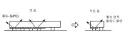
고정된 광 출력 레벨에 대하여, 비용을 감소시키기 위한 주요 수단은 상기 조명 제품에 필요한 상기 LED 반도체 면적을 감소시키는 것이다. 전체 LED 칩 면적의 감소는 최종 제품 조립체에 사용되는 광학 및 다른 컴포넌트들의 크기를 감소시키는 동시에 반도체 제조 설비 생산량을 효과적으로 증가시킨다. 칩 크기의 감소는 전류 밀도를 증가시키지만, 이하 설명되는 본 발명의 에피택셜 기술들을 이용하여 높은 외부 양자 효율이 고 전류 밀도에서 유지될 수 있다. 또한, 칩 설계는 중요한 역할을 한다. 칩 크기가 감소함에 따라 제조 공차들이 활성 면적 활용도를 감소시킬 수 있기 때문에, 수평형 칩들(상부 또는 기판 방출)에 대한 칩 크기 감소는 문제가 있다.For a fixed light output level, the main means for reducing costs is to reduce the LED semiconductor area required for the lighting product. Reducing the overall LED chip area effectively increases semiconductor manufacturing equipment yield while reducing the size of the optics and other components used in the final product assembly. Reducing the chip size increases the current density, but high external quantum efficiency can be maintained at high current density using the epitaxial techniques of the present invention described below. In addition, chip design plays an important role. Chip size reduction for horizontal chips (top or substrate emission) is problematic because manufacturing tolerances can reduce active area utilization as chip size decreases.
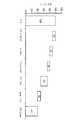
이러한 효과는 도 1에 도시된다. 수평형-분사 장치들(상부 접촉되든지 하부 접촉되든지)은 상기 장치의 동일 측 상에 애노드 및 캐소드 모두를 형성하기 위한 면적이 필요하다. 이는 본질적으로 활성 면적 활용도를 감소시키고(상기 다이 풋 프린트(footprint)의 일부들이 상기 캐소드를 위해 필요하다), 다이 크기를 실질적으로 제한한다. 5 ㎛의 리소그래피 오차, 25 ㎛의 다이-접착 오차, 및 75 ㎛의 범프 직경을 가정하면, 상기 활성 면적 활용도 대 칩 폭은 상기 도면에 도시된 바와 같다. SiC에 대하여, 전도성 버퍼층 접근법은 수직형 분사 설계의 사용을 허용한다. 그러나, SiC와 GaN 사이의 격자 부조화는 고 전력 밀도(high power density)들에서 비신뢰성을 야기할 수 있는 고 전위 밀도들(high dislocation densities)(> 1x10⁸ ㎝2)을 초래한다. 또한, SiC는 GaN 보다 더 높은 굴절률을 가지며, 광 추출의 문제를 더욱 어려운 문제로 만든다.This effect is shown in FIG. Horizontal-injection devices (whether top contacted or bottom contacted) require an area to form both an anode and a cathode on the same side of the device. This essentially reduces active area utilization (some of the die footprint is needed for the cathode) and substantially limits die size. Assuming a lithography error of 5 μm, a die-adhesion error of 25 μm, and a bump diameter of 75 μm, the active area utilization versus chip width is as shown in the figure. For SiC, the conductive buffer layer approach allows the use of a vertical spray design. However, the lattice mismatch between SiC and GaN results in high dislocation densities (> 1 ×10 8 cm2 ) which can cause unreliability at high power densities. In addition, SiC has a higher refractive index than GaN, making the problem of light extraction more difficult.
본 발명은 표면 영역을 갖는 벌크 갈륨 및 질소 함유 기판을 포함하는 발광 다이오드를 제공한다. 하나 이상의 활성 영역들이 상기 표면 영역 위에 놓여 형성되며, 상기 하나 이상의 활성 영역들의 특징인 약 175 암페어/㎠보다 큰 전류 밀도를 갖는다. 상기 장치는 40%(또는 50%, 60%, 70%, 80%, 90%) 이상의 외부 양자 효율(external quantum efficiency; EQE)을 갖는다.The present invention provides a light emitting diode comprising a bulk gallium and nitrogen containing substrate having a surface area. One or more active regions are formed overlying the surface region and have a current density greater than about 175 amps /
대안적인 실시예에서, 본 발명은 대안적인 형태의 발광 다이오드를 제공하지만, 이는 또한 벌크 갈륨 및 질소 함유 기판 및 상기 표면 영역 위에 놓여 형성되는 하나 이상의 활성 영역들을 포함한다. 또한, 상기 장치는 상기 활성 영역들의 특징인 200 A/㎠보다 큰 전류 밀도, 및 385 - 480 ㎚의 파장을 특징으로 하는 방출을 갖는다. 특정 실시예에서, 상기 장치는 백색 광원을 제공하기 위해 상기 주 장치에 실시 가능하게 결합되는 원하는 적색, 녹색, 청색 및 다른 방출 형광체 재료들을 갖는다.In an alternative embodiment, the present invention provides an alternative type of light emitting diode, but it also includes a bulk gallium and nitrogen containing substrate and one or more active regions formed over the surface region. The device also has a current density greater than 200 A /
다른 실시예에서, 본 발명은 무-극성 배향을 갖는 벌크 갈륨 및 질소 함유 기판을 갖는 발광 다이오드를 제공한다. 또한, 상기 장치는 상기 표면 영역 위에 놓여 형성되는 활성 영역들 및 상기 활성 영역들의 특징인 약 500 A/㎠보다 큰 전류 밀도를 갖는다. 상기 장치는 385 - 415 ㎚의 파장을 특징으로 하는 방출 및 백색 광원을 제공하기 위해 실시 가능하게 결합되는 하나 이상의 RGB 또는 다른 색 형광체 재료들을 갖는다. 추가 특정 실시예에서, 상기 장치는 상기 활성 영역들의 특징인 약 500 A/㎠보다 큰 전류 밀도 및 385 - 415 ㎚의 파장을 특징을 하는 방출을 갖는다.In another embodiment, the present invention provides a light emitting diode having a bulk gallium and nitrogen containing substrate having a non-polar orientation. In addition, the device has active regions overlying the surface area and a current density greater than about 500 A /
추가 실시예들에서, 본 발명은 상술한 형태의 발광 다이오드를 작동하는 방법을 제공한다. 상기 방법은 상기 활성 영역들의 접합 영역이 약 200 A/㎠보다 큰 전류 밀도를 제공하고, 385 -480 ㎚의 파장을 갖는 전자기 방사를 출력하도록 상기 장치를 전류 하에 둔다(subject). 상기 장치는 바람직하게는 적어도 상기 벌크 갈륨 및 질소 함유 기판 및 상기 활성 영역들을 둘러쌓는(enclosing) 패키지를 포함한다. 바람직하게는, 상기 패키지는 와트당 15 또는 10 또는 5 또는 1 도 이하의 열 저항을 특징으로 한다.In further embodiments, the present invention provides a method of operating a light emitting diode of the type described above. The method subjects the device under current such that the junction area of the active regions provides a current density of greater than about 200 A /
다른 실시예에서, 상기 발광 다이오드는 상기 하나 이상의 활성 영역들의 특징인 175 암페어/㎠보다 큰 전류 밀도를 갖는다. 게다가, 상기 장치는 적어도 50%의 내부 양자 효율(internal quantum efficiency; IQE); 및 상기 전류 밀도에서 동작 가능한 적어도 약 5000 시간의 수명을 갖는다.In another embodiment, the light emitting diode has a current density greater than 175 amps /
게다가, 본 발명은 발광 다이오드를 제조하기 위한 방법을 제공한다. 상기 방법은 표면 영역을 갖는 벌크 갈륨 및 질소 함유 기판을 제공하는 단계 및 상기 표면 영역 위에 제 1 에피택셜 재료를 형성하는 단계를 포함한다. 또한, 상기 장치는 약 175 암페어/㎠보다 큰 전류 밀도를 위해 바람직하게 구성된 상기 에피택셜 재료 위에 놓여 형성되는 하나 이상의 활성 영역들을 포함한다. 또한, 상기 방법은 상기 활성 영역들 위에 놓여 제 2 에피택셜 재료를 형성하는 단계 및 콘택 영역들을 형성하는 단계를 포함할 수 있다.In addition, the present invention provides a method for manufacturing a light emitting diode. The method includes providing a bulk gallium and nitrogen containing substrate having a surface area and forming a first epitaxial material over the surface area. The device also includes one or more active regions formed overlying the epitaxial material, which are preferably configured for current densities greater than about 175 amps /
본 발명은 상기 활성 면적의 특징인 50%보다 큰 활성 면적 활용도를 갖는 LED 광학 장치를 제공한다. 다른 실시예들에서, 상기 활용도는 > 80%, > 90%, 또는 > 95%이다. 또한, 본 발명은 활성 영역 면적에 대한 상기 방출 외부 표면적의 특징인 1보다 큰 비율을 갖는 장치를 허용하며, 다른 실시예들에서, 상기 비율은 > 5, > 10 , 또는 > 100이다.The present invention provides an LED optical device having an active area utilization greater than 50% that is characteristic of the active area. In other embodiments, the utilization is> 80%,> 90%, or> 95%. In addition, the present invention allows devices having a ratio greater than 1, which is characteristic of the emission outer surface area to active area area, in other embodiments, the ratio is> 5,> 10, or> 100.
게다가, 본 발명은 장치, 예를 들면, 백열 전구 또는 등기구(fixture)를 제공한다. 상기 장치는 약 1 ㎟보다 작은 누적 다이 표면적을 갖고, 적어도 300 루멘을 방출도록 구성되는 하나 이상의 LED들을 갖는다. 특정 실시예에서, 상기 LED들은 반-극성, 극성 또는 무-극성 배향을 갖는 벌크 갈륨 및 질소 함유 재료로 제조되는 단일 LED로 구성된다. 하나 보다 많은 LED가 제공되는 경우, 이들은 바람직하게는 배열로 구성된다.In addition, the present invention provides an apparatus, for example an incandescent bulb or a fixture. The apparatus has a cumulative die surface area of less than about 1
일반적으로 상기 LED는 약 1 ㎜2보다 작은 활성 접합 면적을 갖는 크기의 활성 접합 면적을 갖으며, 이는 약 0.75 ㎜2보다 작고, 약 0.5 ㎜2보다 작으며, 약 0.3 ㎜2보다 작다. 특정 실시예에서, 상기 장치는 적어도 300 루멘, 적어도 500 루멘, 적어도 700 루멘을 방출한다. 특정 실시예에서, 상기 방출은 실질적으로 백색광, 또는 390 - 415 ㎚, 415 - 440 ㎚, 440 - 470 ㎚ 등의 범위이다. 다른 실시예들에서, 상기 LED는 2 와트/㎜2보다 크거나, 3 와트/㎜2보다 크거나, 5 와트/㎜2보다 크거나, 10 와트/㎜2보다 크거나, 15 와트/㎜2보다 크거나, 20와트/㎜2보다 크거나, 또는 그외의 활성 접합 면적당 입력 전력을 특징으로 한다. 상기 실시예에 따르면, 상기 LED는 약 5000K보다 작은 CCT 및 약 75보다 큰 CRI를 갖는 온백색(warm white) 방출에 대하여 300 ㏐/㎜2,보다 큰 활성 접합 면적당 루멘을 특징으로 한다. 대안적으로, 상기 LED는 약 5000K보다 큰 CCT 및 약 75보다 큰 CRI를 갖는 온백색 방출에 대하여 400 ㏐/㎜2보다 큰 활성 접합 면적당 루멘을 특징으로 한다. 대안적으로, 상기 LED는 약 5000K보다 큰 CCT 및 약 75보다 큰 CRI를 갖는 온백색 방출에 대하여 600 ㏐/㎜2보다 큰 활성 접합 면적당 루멘을 특징으로 한다. 대안적으로, 상기 LED는 약 5000K보다 큰 CCT 및 약 75보다 큰 CRI를 갖는 온백색 방출에 대하여 800 ㏐/㎜2보다 큰 활성 접합 면적당 루멘을 특징으로 한다.Generally the LED has an active junction area of a size having an active junction area of less than about 1 mm2 , which is less than about 0.75 mm2, less than about 0.5 mm2, and less than about 0.3 mm2 . In certain embodiments, the device emits at least 300 lumens, at least 500 lumens, at least 700 lumens. In certain embodiments, the emission is substantially white light, or in the range of 390-415 nm, 415-440 nm, 440-470 nm, and the like. In other embodiments, the LED is greater than 2 Watts / mm2, greater than 3 Watts / mm2, greater than 5 Watts / mm2, greater than 10 Watts / mm2 , or 15 Watts / mm2 Or input power per active junction area greater than 20 watts / mm2 or otherwise. According to this embodiment, the LED is characterized by a lumen per active junction area of greater than 300 mW / mm2 for warm white emission with a CCT less than about 5000K and a CRI greater than about 75K. Alternatively, the LEDs are characterized by lumens per active junction area greater than 400 mm3 / mm2 for warm white emission with a CCT greater than about 5000K and a CRI greater than about 75K. Alternatively, the LEDs are characterized by lumens per active junction area greater than 600 mm3 / mm2 for warm white emission with a CCT greater than about 5000K and a CRI greater than about 75K. Alternatively, the LEDs are characterized by lumens per active junction area greater than 800 mm3 / mm2 for warm white emission with a CCT greater than about 5000K and a CRI greater than about 75K.
본 명세서에서 설명되는 상기 LED들은 상기 활성 영역들의 특징인 175 암페어/㎠보다 큰 전류 밀도 및 미리 결정된 증가된 동작 전류 밀도에서 상기 값과 비교하여 최대값에서 측정될 때, 절대 효율로 약 5%보다 작은 롤오프(roll-off)를 특징으로 하는 외부 양자 효율, 및 390 - 480 ㎚의 파장을 특징으로 하는 방출을 가질 수 있다.The LEDs described herein are greater than about 5% in absolute efficiency when measured at maximum value compared to the value at a predetermined increased operating current density and a current density greater than 175 amps /
본 LED는 100℃보다 크거나, 150℃보다 크거나, 및/또는 200℃보다 크거나, 및 훨씬 높은 접합 온도에서 동작 가능하다. 바람직한 실시예들에서, 본 장치는 비냉각(un-cooled) 상태로 및 연속파(continuous wave) 동작하에서 동작 가능하다. 또한, 본 LED는 약 175 A/㎠에서 약 1KA/㎠ 이상까지의 범위일 수 있는 전류 밀도를 갖는다. 하나 이상의 바람직한 실시예들에서, 상기 전류 밀도는 또한 약 400 A/㎠ 내지 800 A/㎠이다.The LED is operable at junction temperatures greater than 100 ° C., greater than 150 ° C., and / or greater than 200 ° C., and much higher. In preferred embodiments, the apparatus is operable in an un-cooled state and under continuous wave operation. The LED also has a current density that can range from about 175 A /
본 명세서의 상기 장치 및 방법은 LED들의 제조시 종래의 기술들에 비하여 높은 수율을 제공한다. 다른 실시예들에서, 본 방법 및 결과로 생기는 구조는 종래의 기술들 및 극성, 무-극성 또는 반-극성 표면 배향들을 갖는 갈륨 및 질소 함유 기판 재료들을 사용하여 형성하기가 더 용이하다. 본 발명은 더 작은 최소 배선 폭들(feature sizes) 및 실질적으로 "드루프" 없는 고 전류 밀도 LED 장치들을 위한 결과로 생기는 장치 및 방법을 제공한다. 바람직한 실시예에서, 상기 장치는 종래의 장치들과 비교하여 실질적으로 감소된 LED 반도체 면적을 사용하는 결과로 생기는 백색광 등기구를 제공한다. 바람직한 실시예에서, 본 LED 활성 영역 설계들은 드루프를 감소시키도록 구성되고, 고 전류 밀도들에서 효율적으로 동작하는 칩 아키텍쳐들을 허용한다.The apparatus and method herein provide higher yields compared to conventional techniques in the manufacture of LEDs. In other embodiments, the present method and resulting structure is easier to form using conventional techniques and gallium and nitrogen containing substrate materials having polar, non-polar or semi-polar surface orientations. The present invention provides the resulting apparatus and method for smaller current sizes and high current density LED devices that are substantially "drop-free". In a preferred embodiment, the device provides a white light luminaire resulting from using a substantially reduced LED semiconductor area compared to conventional devices. In a preferred embodiment, the present LED active area designs are configured to reduce droop and allow chip architectures to operate efficiently at high current densities.
본 발명의 특성 및 장점들의 추가 이해는 명세서 및 첨부된 도면들을 참조하여 달성될 수 있다.Further understanding of the features and advantages of the present invention may be achieved with reference to the specification and the accompanying drawings.
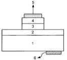
도 1은 본 발명의 실시예에 따른 (a) 수평형 분사(예를 들면, 도시된 플립-칩), (b) 수직형 박막, 및 (c) 벌크-기판 기반 LED들에 대한 칩 크기의 간략화된 도시이다.
도 2는 5 ㎛의 리소그래피 오차, 25 ㎛의 다이-접착 오차, 및 75 ㎛의 범프 직경을 가정하고, 본 발명과 비교하여 수평형 칩 설계들에 대한 칩 폭의 함수로서 활성 면적 활용도(장치 풋 프린트에 대한 활성 면적의 비)를 도시한다.
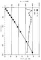
도 3은 25 ℃의 접합 온도를 갖는 종래의 LED, 크리(Cree) XP-E 백색 LED에 대한 분사 전류의 함수로서 상대 광속의 예시 플롯(plot)을 도시한다.
도 4는 (a) 2개의 2.5 나노미터 우물들을 갖는 다중 양자 우물 LED, (b) 6개의 2.5 나노미터 양자 우물들을 갖는 다중 양자 우물 LED, 및 (c) 13 나노미터 활성 영역을 갖는 이중 헤테로구조(double heterostructure) LED에 대한 전류 밀도의 함수로서 외부 양자 효율을 도시한다. LED들의 각각은 ~430 ㎚에서의 방출을 나타내었다.
도 4A는 본 발명의 실시예에 따른 LED 장치들에 대한 전류 밀도에 대비하여 그려진 양자 효율을 도시한다.
도 5는 본 발명의 실시예에 따른 고 전류 밀도 에피택셜적으로(epitaxially) 성장된 LED 구조의 간략화된 다이어그램이다.
도 5A는 본 발명의 하나 이상의 실시예들에 따른 에피택셜 증착 공정의 간략화된 흐름도이다.
도 6은 본 발명의 실시예에 따른 전기적 연결들을 갖는 고 전류 밀도 LED 구조를 도시하는 간략화된 다이어그램이다.
도 7은 본 발명의 실시예에 따른 하부-방출 수평 전도 고 전류 밀도 LED 장치의 간략화된 다이어그램이다.
도 8은 본 발명의 특정 실시예에 따른 하부-방출 수직 전도 고 전류 밀도 LED 장치의 간략화된 다이어그램이다.
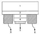
도 9는 본 발명의 실시예에 따른 고 전류 밀도 LED를 함유하는 패키징된 백색 LED의 간략화된 예시이다.
도 10은 본 발명의 실시예들에 따른 ~405 ㎚의 발광 파장을 갖는 무-극성 GaN 상에 제조된 LED에 대한 펄스 출력 전력 대 전류 밀도 및 외부 양자 효율 대 전류 밀도를 도시하는 간략화된 다이어그램이다.
도 11 내지 도 15는 본 발명의 실시예들에 따른 LED 장치들에 대한 실험 결과들이다.1 illustrates chip size for (a) horizontal jet (eg, flip-chip shown), (b) vertical thin film, and (c) bulk-substrate based LEDs in accordance with an embodiment of the present invention. It is a simplified city.
FIG. 2 assumes a lithography error of 5 μm, a die-glue error of 25 μm, and a bump diameter of 75 μm, and active area utilization (device foot) as a function of chip width for horizontal chip designs compared to the present invention. Ratio of active area to print).
3 shows an example plot of relative luminous flux as a function of injection current for a conventional LED, Cree XP-E white LED, having a junction temperature of 25 ° C. FIG.
4 shows (a) a multi quantum well LED with two 2.5 nanometer wells, (b) a multi quantum well LED with six 2.5 nanometer quantum wells, and (c) a dual heterostructure with 13 nanometer active area (double heterostructure) Shows external quantum efficiency as a function of current density for the LED. Each of the LEDs exhibited an emission at ˜430 nm.
4A shows quantum efficiency plotted against current density for LED devices in accordance with an embodiment of the present invention.
5 is a simplified diagram of a high current density epitaxially grown LED structure in accordance with an embodiment of the present invention.
5A is a simplified flow diagram of an epitaxial deposition process in accordance with one or more embodiments of the present invention.
6 is a simplified diagram illustrating a high current density LED structure with electrical connections in accordance with an embodiment of the present invention.
7 is a simplified diagram of a bottom-emitting horizontal conducting high current density LED device according to an embodiment of the present invention.
8 is a simplified diagram of a bottom-emitting vertical conduction high current density LED device in accordance with certain embodiments of the present invention.
9 is a simplified illustration of a packaged white LED containing a high current density LED according to an embodiment of the invention.
FIG. 10 is a simplified diagram showing pulse output power versus current density and external quantum efficiency versus current density for LEDs fabricated on non-polar GaN with emission wavelengths of 405 nm in accordance with embodiments of the present invention. .
11 to 15 are experimental results of LED devices according to embodiments of the present invention.
본 발명은 일반적으로 조명 기술들에 관한 것으로, 특히, 벌크 갈륨 및 질소 함유 극성, 반-극성 또는 무-극성 재료들 상에 제조되는 고 전류 밀도 LED 장치들용 기술들에 관한 것이다. 본 발명은 백색 조명, 다색 조명, 평판 디스플레이들을 위한 조명, 다른 광전자 장치들, 및 유사한 제품들과 같은 응용들에 적용될 수 있다.FIELD OF THE INVENTION The present invention relates generally to lighting techniques, and more particularly to techniques for high current density LED devices fabricated on bulk gallium and nitrogen containing polar, semi-polar or non-polar materials. The present invention can be applied to applications such as white illumination, multicolor illumination, illumination for flat panel displays, other optoelectronic devices, and similar products.
본 출원인은 GaN-기반 광전자 공학 분야에서 최근의 큰 발전이 벌크 극성, 무-극성 및 반-극성 GaN 기판들 상에 제조된 장치들의 탁월한 잠재력을 증명하였음을 알게 되었다. 특히, 무-극성 및 반-극성 배향들에 대해, c-평면 GaN 상의 종래의 장치들을 괴롭히는 전계들이 유도되는 강한 분극화의 부족은 상기 발광 InGaN 층들에서 크게 향상된 방사성 재결합 효율을 초래한다. 극성 재료들에 대하여, 분극장들(polarization fields)의 유해한 효과들은 상기 활성 영역의 InN 함량을 감소시키고, 및/또는 다중 양자 우물(multi-quantum well; MQW) 활성 영역 구조들에서 배리어 두께를 감소시킴으로써 감소될 수 있다. 또한, 임의의 표면 배향에 대하여, 상기 벌크 천연 기판은 사파이어 SiC 또는 Si 와 같은 이질 기판들에 기반한 접근법들과 비교하여 적은 비용(루멘당 달라로)을 제공하기 위해 축소시킬 수 있는 간략화된 장치 기하형상을 제공한다. 게다가, 벌크 GaN에 의해 제공되는 감소된 전위 밀도들은 고 전류 밀도들에서 고 신뢰성의 보증을 제공하는데, 이는 이질 기판 접근법들에 의해 보증되지 않다.Applicant has found that recent significant developments in the field of GaN-based optoelectronics have demonstrated the excellent potential of devices fabricated on bulk polar, non-polar and semi-polar GaN substrates. In particular, for non-polar and semi-polar orientations, the lack of strong polarization inducing electric fields that plague conventional devices on c-plane GaN results in greatly improved radioactive recombination efficiency in the luminescent InGaN layers. For polar materials, the deleterious effects of polarization fields reduce the InN content of the active region and / or reduce the barrier thickness in multi-quantum well (MQW) active region structures. Can be reduced. In addition, for any surface orientation, the bulk natural substrate is a simplified device geometry that can be scaled down to provide lower cost (in different per lumen) compared to approaches based on heterogeneous substrates such as sapphire SiC or Si. Provide the shape. In addition, the reduced dislocation densities provided by bulk GaN provide a guarantee of high reliability at high current densities, which is not guaranteed by heterogeneous substrate approaches.
무-극성 및 반-극성 GaN 기판들 상에 제조되는 발광 다이오드(LED)의 발전은 조명의 분야에 대해 특히 중요하다. InGaN 발광층들을 사용하는 이런 장치들은 청자색 영역(390 - 430 ㎚), 청색 영역(430 - 490 ㎚), 녹색 영역(490 - 560 ㎚), 및 황색 영역(560 - 600 ㎚)으로 확장되는 동작 파장들에서 기록적인 출력 전력들 나타내왔다. 예를 들면, 402 ㎚의 피크 방출 파장을 갖는 청자색 LED는 최근 m-평면(1-110) GaN 기판 상에서 제조되었고, 광 추출 향상 특징들을 갖지 않음에도 불구하고 45%보다 큰 외부 양자 효율을 증명하였으며, 고 전류 밀도들에서 최소한의 롤오버(roll-over)를 갖는 우수한 성능을 나타내었다[K.-C.Kim, M.C.Schmidt, H.Sato, F.Wu, N.Fellows, M.Saito, K.Fujito, J.S.Speck, S.Nakamura, and S.P.DenBaars, "Improved electroluminescence on nonpolar m-plane InGaN/GaN quantum well LEDs", Phys.Stat.Sol.(RRL) 1, No.3, 125 (2007).]. 유사하게, 468 ㎚의 피크 방출 파장을 갖는 청색 LED는 고 전력 밀도들에서 우수한 효율 및 c-평면 LED들에 대해 일반적으로 관찰되는 것보다 상당히 적은 롤오버를 나타내었다[K.Iso, H.Yamada, H.Hirasawa, N.Fellows, M.Saito, K.Fujito, S.P.DenBaars, J.S.Speck, and S.Nakamura, "High brightness blue InGaN/GaN light emitting diode on nonpolar m-plane bulk GaN substrate", Japanese Journal of Applied Physics 46, L960 (2007).]. 2개의 유망한 반-극성 배향들은 (10-1-1) 및 (11-22) 평면들이다. 이 평면들은 상기 c-평면에 대하여 각각 62.0 도 및 58.4 도로 경사진다. 캘리포니아 산타 바바라 대학(University of California, Santa Barbara; UCSB)은 청색-방출 장치들에 대해 100 ㎃에서 65 ㎽ 이상의 출력 전력을 갖는(10-1-1) GaN[H.Zhong, A.Tyagi, N.Fellows, F.Wu, R.B.Chung, M.Saito, K.Fujito, J.S.Speck, S.P.DenBaars, and S.Nakamura, "High power and high efficiency blue light emitting diode on freestanding semipolar (1011) bulk GaN substrate", Applied Physics Letters 90, 233504 (2007)] 및 청-녹색 방출 장치들에 대해 100 ㎃에서 35 ㎽ 이상의 출력 전력[H.Zhong, A.Tyagi, N.N.Fellows, R.B.Chung, M.Saito, K.Fujito, J.S.Speck, S.P.DenBaars, and S.Nakamura, Electronics Lett.43, 825 (2007)], 녹색-방출 장치들에 대해 100 ㎃에서 15 ㎽ 이상의 출력[H.Sato, A.Tyagi, H.Zhong, N.Fellows, R.B.Chung, M.Saito, K.Fujito, J.S.Speck, S.P.DenBaars, and S.Nakamura, "High power and high efficiency green light emitting diode on free-standing semipolar (1122) bulk GaN substrate", Physical Status Solidi - Rapid Research Letters 1, 162 (2007)] 및 황색 장치들에 대해 15 ㎽ 이상[H.Sato, R.B.Chung, H.Hirasawa, N.Fellows, H.Masui, F.Wu, M.Saito, K.Fujito, J.S.Speck, S.P.DenBaars, and S.Nakamura, "Optical properties of yellow light-emitting diodes grown on semipolar (1122) bulk GaN substrates," Applied Physics Letters 92, 221110 (2008).]을 갖는 (11-22) GaN 상에서 매우 효율적인 LED들을 제조했었다. 상기 UCSB 그룹은 반-극성 (11-22) GaN 상의 인듐 결합이 c-평면 GaN의 것보다 동등하거나 크다는 것을 제시했었으며, 이는 InGaN 층들에서 방출하는 파장이 확장된 높은 결정 품질을 달성하기 위한 추가 가능성을 제공한다.The development of light emitting diodes (LEDs) fabricated on non-polar and semi-polar GaN substrates is particularly important for the field of lighting. Such devices using InGaN emitting layers extend operating wavelengths to the blue violet region (390-430 nm), the blue region (430-490 nm), the green region (490-560 nm), and the yellow region (560-600 nm). The record output powers are shown in. For example, a blue-violet LED with a peak emission wavelength of 402 nm was recently fabricated on an m-plane (1-110) GaN substrate and demonstrated external quantum efficiencies greater than 45% despite no light extraction enhancement features. , Good performance with minimal roll-over at high current densities [K.-C.Kim, MCSchmidt, H.Sato, F.Wu, N.Fellows, M.Saito, K. Fujito, JSSpeck, S. Nakamura, and SPDenBaars, "Improved electroluminescence on nonpolar m-plane InGaN / GaN quantum well LEDs", Phys. Stat. Sol. (RRL) 1, No. 3, 125 (2007).] . Similarly, blue LEDs with a peak emission wavelength of 468 nm exhibited good efficiency at high power densities and significantly less rollover than generally observed for c-plane LEDs [K.Iso, H.Yamada, H.Hirasawa, N.Fellows, M.Saito, K.Fujito, SPDenBaars, JSSpeck, and S.Nakamura, "High brightness blue InGaN / GaN light emitting diode on nonpolar m-plane bulk GaN substrate", Japanese Journal of Applied Physics 46, L960 (2007).]. Two promising semi-polar orientations are (10-1-1) and (11-22) planes. These planes are inclined at 62.0 degrees and 58.4 degrees with respect to the c-plane, respectively. The University of California, Santa Barbara (UCSB), GaN [H.Zhong, A.Tyagi, N, has an output power of 100 to 65 mA or more for blue-emitting devices (10-1-1). Fellows, F.Wu, RBChung, M.Saito, K.Fujito, JSSpeck, SPDenBaars, and S. Nakamura, "High power and high efficiency blue light emitting diode on freestanding semipolar (1011) bulk GaN substrate", Applied Physics Letters 90, 233504 (2007) and more than 35 kW output power for H.Zhong, A.Tyagi, NNFellows, RBChung, M.Saito, K.Fujito, JSSpeck, SPDenBaars, and S. Nakamura, Electronics Lett. 43, 825 (2007)], outputs from 100 Hz to more than 15 Hz for green-emitting devices [H.Sato, A.Tyagi, H.Zhong, N Fellows, RBChung, M. Saito, K.Fujito, JSSpeck, SPDenBaars, and S. Nakamura, "High power and high efficiency green light emitting diode on free-standing semipolar (1122) bulk GaN substrate", Physical Status Solidi-Rapid Research Letters 1, 162 (2007)] and at least 15 mm for yellow devices [H.Sato, RBChung, H.Hirasawa, N.Fellows, H.Masui, F.Wu, M.Saito, K.Fujito, JSSpeck, SPDenBaars, and S. Nakamura, (11-22) GaN with "Optical properties of yellow light-emitting diodes grown on semipolar (1122) bulk GaN substrates," Applied Physics Letters 92, 221110 (2008).] LEDs have been made very efficient. The UCSB group suggested that the indium bonds on the semi-polar (11-22) GaN are equal or larger than those of c-plane GaN, which is a further possibility to achieve high crystal quality with extended wavelengths emitted in InGaN layers. To provide.
무-극성 또는 반-극성 LED는 벌크 갈륨 질화물 기판 상에 제조될 수 있다. 상기 갈륨 질화물 기판은 공지된 방법에 따라 수소화물 기상 에피택시에 의해 또는 아모노서멀적으로(ammonothermally) 성장되었던 부울(boule)로부터 슬라이스될(sliced) 수 있다. 일 특정 실시예에서, 공동으로 양도되었으며, 본 명세서에는 참조로 포함되는 미국 특허 출원 제61/078,704호에 개시된 바와 같이, 상기 갈륨 질화물 기판은 수소화물 기상 에피택시와 아모노서멀 성장의 조합에 의해 제조된다. 상기 부울은 단결정 시드(seed) 결정상에서 c-방향, m-방향, a-방향 또는 반-극성 방향으로 성장될 수 있다. 반-극성 평면들은 (hkil) 밀러 지수들에 의해 표기될 수 있으며, 여기서 i=-(h+k), l은 0이 아니며, h 및 k 중 적어도 하나는 영이 아니다. 상기 갈륨 질화물 기판은 절단(cut), 래핑(lapped), 연마 및 기계-화학적으로 연마될 수 있다. 상기 갈륨 질화물 기판 배향은 {1 -1 0 0} m 평면, {1 1 -2 0} a 평면, {1 1 -2 2} 평면, {2 0 -2 ±1} 평면, {1 -1 0 ±1} 평면, {1 0 -1 ±1} 평면, {1 -1 0 ±2} 평면 또는 {1 -1 0 ±3} 평면의 ±5 도, ±2 도, ±1 도 또는 ±0.5 도 이내 일 수 있다. 상기 갈륨 질화물 기판은 대면적 표면의 평면에서 106 ㎝-2보다 작거나, 105 ㎝-2보다 작거나, 104 ㎝-2보다 작거나, 또는 103 ㎝-2보다 작은 전위 밀도를 가질 수 있다. 상기 갈륨 질화물 기판은 c 평면에서 106 ㎝-2보다 작거나, 105 ㎝-2보다 작거나, 104 ㎝-2보다 작거나, 또는 103 ㎝-2보다 작은 전위 밀도를 가질 수 있다.Non-polar or semi-polar LEDs can be fabricated on bulk gallium nitride substrates. The gallium nitride substrate can be sliced from boules that have been grown by hydride gas phase epitaxy or ammonothermally according to known methods. In one particular embodiment, the gallium nitride substrate is formed by a combination of hydride vapor phase epitaxy and anothermal growth, as disclosed in US patent application Ser. No. 61 / 078,704, which is commonly assigned and is incorporated herein by reference. Are manufactured. The boolean can be grown in c-, m-, a- or semi-polar directions on a single crystal seed crystal. Semi-polar planes can be denoted by (hkil) Miller indices, where i =-(h + k), l is not zero and at least one of h and k is not zero. The gallium nitride substrate can be cut, lapped, polished and mechano-chemically polished. The gallium nitride substrate orientation is {1 -1 0 0} m plane, {1 1 -2 0} a plane, {1 1 -2 2} plane, {2 0 -2 ± 1} plane, {1 -1 0 ± 1 degree plane, {1 0 -1 ± 1} plane, {1 -1 0 ± 2} plane, or {1 -1 0 ± 3} plane ± 5 degrees, ± 2 degrees, ± 1 degrees, or ± 0.5 degrees Can be within. The gallium nitride substrate has a dislocation density of less than 106 cm-2, less than 105 cm-2, less than 104 cm-2 , or less than 103 cm-2 in the plane of the large area surface. Can be. The gallium nitride substrate may have a dislocation density of less than 106 cm−2, less than 105 cm−2, less than 104 cm−2 , or less than 103 cm−2 in the c plane.
호모에피택셜(homoepitaxial) 무-극성 또는 반-극성 LED는 공지된 방법들, 예를 들면, 그 전체가 참조로 포함되는 미국 특허 제7,053,413호에 개시된 다음의 방법들에 따라 상기 갈륨 질화물 기판 상에 제조된다. 적어도 하나의 AlxInyGa1-x-yN 층, 여기서, 0 ≤ x ≤ 1, 0 ≤ y ≤ 1, 및 0 ≤ x+y ≤ 1,은 예를 들면, 그 전체가 참조로 포함되는 미국 특허들 제7,338,828호 및 제 7,220,324호에 의해 개시되는 다음의 방법들로 상기 기판 상에 증착된다. 상기 적어도 하나의 AlxInyGa1-x-yN 층은 금속 유기 화학적 기상 증착, 분자선 에피택시, 수소화물 기상 에피택시, 또는 이들의 조합에 의해 증착될 수 있다. 일 실시예에서, 상기 AlxInyGa1-x-yN 층은 전류가 그것을 통과할 때 광을 우선적으로 방출하는 활성층을 포함한다. 일 특정 실시예에서, 상기 활성층은 약 0.5 ㎚와 약 40 ㎚ 사이의 두께를 갖는 단일 양자 우물을 포함한다. 특정 실시예에서, 상기 활성층은 약 1 ㎚와 약 5 ㎚ 사이의 두께를 갖는 단일 양자 우물을 포함한다. 다른 실시예들에서, 상기 활성층은 약 5 ㎚와 약 10 ㎚ 사이, 약 10 ㎚와 약 15 ㎚ 사이, 약 15 ㎚와 약 20 ㎚ 사이, 약 20 ㎚와 약 25 ㎚ 사이, 약 25 ㎚와 약 30 ㎚ 사이, 약 30 ㎚와 약 35 ㎚ 사이, 또는 약 35 ㎚와 약 40 ㎚ 사이의 두께를 갖는 단일 양자 우물을 포함한다. 다른 일련의 실시예들에서, 상기 활성층은 다중 양자 우물을 포함한다. 또 다른 실시예에서, 상기 활성층은 약 40 ㎚와 약 500 ㎚ 사이의 두께를 갖는 이중 헤테로구조를 포함한다. 일 특정 실시예에서, 상기 활성층은 InyGa1-yN 층을 포함하는데, 여기서, 0 ≤ y ≤ 1이다. 물론, 다른 변형들, 수정들 및 대안들이 있을 수 있다.A homoepitaxial non-polar or semi-polar LED is mounted on the gallium nitride substrate according to known methods, for example, the following methods disclosed in US Pat. No. 7,053,413, which is incorporated by reference in its entirety. Are manufactured. At least one Alx Iny Ga1-xy N layer, where 0 ≦ x ≦ 1, 0 ≦ y ≦ 1, and 0 ≦ x + y ≦ 1, for example, the United States of which is incorporated by reference in its entirety. It is deposited on the substrate by the following methods disclosed by patents 7,338,828 and 7,220,324. The at least one ofAl x In y Ga 1 -x- y N layer may be deposited by metal organic chemical vapor deposition, molecular beam epitaxy, hydride vapor phase epitaxy, or a combination thereof. In one embodiment, the Alx Iny Ga1-xy N layer comprises an active layer that preferentially emits light as current passes through it. In one particular embodiment, the active layer comprises a single quantum well having a thickness between about 0.5 nm and about 40 nm. In certain embodiments, the active layer comprises a single quantum well having a thickness between about 1 nm and about 5 nm. In other embodiments, the active layer is between about 5 nm and about 10 nm, between about 10 nm and about 15 nm, between about 15 nm and about 20 nm, between about 20 nm and about 25 nm, about 25 nm and about A single quantum well having a thickness between 30 nm, between about 30 nm and about 35 nm, or between about 35 nm and about 40 nm. In other series of embodiments, the active layer comprises multiple quantum wells. In yet another embodiment, the active layer comprises a double heterostructure having a thickness between about 40 nm and about 500 nm. In a particular embodiment, the active layer is Iny Ga1- comprises ay N layer, where a 0 ≤ y ≤ 1. Of course, there may be other variations, modifications and alternatives.
게다가, 발광 다이오드 내의 입력 전류가 증가됨에 따라, 관련된 보다 큰 수의 분사된 전자들이 광자로 변환되기 때문에 광 출력 전력이 증가한다. "이상적인" LED에서, 상기 광 출력은 작은 LED들이 고 출력 전력을 달성하기 위해 매우 높은 전류 밀도들로 구동될 수 있도록 증가된 전류에 대해 선형적인 증가가 지속될 것이다. 그러나, 실제로 발광 다이오드들의 이러한 광 출력 대 전류 입력 특성은 종래의 발광 다이오드들의 방사 효율이 상기 전류 밀도가 증가함에 따라 감소하는 현상에 의해 근본적으로 제한되어 버린다. 이런 형상들은 출력 전력 대 전류의 롤오버 또는 서브리니어(sublinear) 증가를 초래함이 알려져 왔다. 이는 상기 입력 전류가 증가됨에 따라 전체 유속(flux)에서의 단지 한계적(marginal) 증가를 초래한다.In addition, as the input current in the light emitting diode increases, the light output power increases because the associated larger number of injected electrons are converted to photons. In an "ideal" LED, the light output will continue to increase linearly with increased current so that small LEDs can be driven at very high current densities to achieve high output power. In practice, however, this light output versus current input characteristic of light emitting diodes is fundamentally limited by the phenomenon that the radiation efficiency of conventional light emitting diodes decreases as the current density increases. Such shapes have been known to result in rollover or sublinear increase in output power versus current. This results in only a marginal increase in overall flux as the input current is increased.
도 3은 종래의 LED, 25 ℃의 접합 온도를 갖는 크리 XP-E 백색 LED에 대한 분사 전류의 함수로서 상대 광속의 예시적인 플롯을 도시한다. 상기 플롯은 700 ㎃에서 상기 상대 광속이 단지 대략 170 %인 반면, 350 ㎃에서 상대 광속(대략 30 - 50 A/㎠)이 100%임을 나타낸다. 이는 종래의 LED에 대하여 상기 LED에 대한 효율에서의 대략 15%의 롤오프는 대략 30 - 50 A/㎠에서 60 - 100 A/㎠까지의 동작 범위를 넘어 발생함을 나타낸다. 게다가, 이러한 다이오드에 대한 피크 효율은 훨씬 낮은 동작 전류 밀도에서 발생하고, 700 ㎃에서 동작되는 상기 다이오드는 피크값으로부터의 효율의 롤오프가 15%보다 훨씬 크다는 것을 보여주고 있었다.FIG. 3 shows an exemplary plot of relative luminous flux as a function of injection current for a conventional LED, CREE XP-E white LED with junction temperature of 25 ° C. FIG. The plot shows that the relative luminous flux is only approximately 170% at 700 Hz, while the relative luminous flux (approximately 30-50 A / cm 2) is 100% at 350 Hz. This indicates that for a conventional LED, a rolloff of approximately 15% in efficiency for the LED occurs over an operating range from approximately 30-50 A /
상기 현상들에 기인하여, 종래의 발광 다이오드들은 일반적으로 본 발명 및 장치들에 의해 제공되는 것보다 낮은 전류 밀도들, 10 A/㎠에서 100 A/㎠까지의 범위에서 동작된다. 이러한 동작 전류 밀도 제한은 단일의 종래 발광 다이오드로부터 가능한 전체 유속에 대한 실제적인 한계들로 평가되어 왔다. LED 패키지로부터 상기 유속을 증가시키는 보통의 접근법들은 상기 LED의 활성 면적의 증가(이에 의해 상기 LED가 적합한 낮은 전류밀도를 유지하면서 더 높은 동작 전류를 갖도록 함), 및 상기 전체 전류가 상기 패키지 내의 상기 LED들 사이에서 분할되도록 다수의 LED 다이를 LED들의 배열로 패키징함을 포함한다. 적절하게 낮은 전류 밀도를 유지하는 동안 이러한 접근법들이 LED 패키지당 더 많은 전체 유속을 발생하는 효과를 갖지만, 이들은 증가된 전체 LED 다이 면적의 요구에 기인하여 본질적으로 보다 많은 비용이 든다. 하나 이상의 실시예들에서, 본 출원인은 긴 동작 수명을 유지하면서도 종래의 LED들을 초과한 전류 밀도들에서 동작하는 고 효율을 제공하는 하나 이상의 작은-칩 고 휘도 LED들에 기반한 조명에 대한 방법 및 장치를 제안한다.Due to the above phenomena, conventional light emitting diodes are generally operated at lower current densities, ranging from 10 A /
효율적인 동작으로 고 전류 밀도에서 동작하는 LED의 제한들의 종래의 지식을 확립하는 광범위한 많은 연구가 있다. 이러한 많은 연구는 가장 큰 LED 제조사들에 상업화되어 왔던 고 휘도 LED들에 대한 동작 전류 밀도에서의 유사성, 및 "LED 드루프" 현상들을 참조한 광범위한 많은 연구를 포함한다. 상용 LED들의 예시들은 도 1에 도시된 하나의 이러한 예시를 갖는 크리의 XP-E, XR-E 및 MC-E 패키지들 및 루미네즈(Lumileds) K2 및 레벨(Rebel) 패키지들을 포함한다. 유사한 고 휘도 LED들은 오스람(Osram), 니치아(Nichia), 아바고(Avago), 브릿지룩스(Bridgelux) 등과 같은 회사로부터 입수할 수 있는데, 이들 모두는 상기 전체 전류의 제한, 1 ㎟ 이상의 다이 크기의 증가, 또는 상기 LED 접합 면적을 효과적으로 증가시키기 위한 다수의 LED 칩들의 패키징 중 어느 하나를 통하여 본 발명에서 제안되는 것보다 훨씬 낮은 전류 밀도 범위에서 동작한다. 상기 LED "드루프" 현상들을 참조 및 제시하는 문헌들의 예시들은 쉔(Shen) 등의 Applied Physics Letters, 91, 141101 (2007) 및 미치유(Michiue) 등의 the Proceedings of the SPIE Vol. 7216, 72161Z-1 (2009)에 의해 예로서 설명된다. 게다가, 가드너(Gardner) 등의 Applied Physics Letters, 91, 243506 (2007)은 이러한 현상들 및 대략 200 A/㎠에서 피크 효율을 나타내고 다음 그 동작점 위에서 롤오프하는 사파이어 기판 상에 성장된 이들의 이중 헤테로구조 LED를 갖는 LED들에 대해 중요한 일반적인 전류 밀도들이 20 - 400 A/㎠임을 극복하기 위한 시도들에 관하여 명쾌하게 명시한다. 게다가, 고 전류 밀도에서 동작하는 동시에 장치 효율을 유지할 때의 제한들에 더하여, 상기 전류 밀도가 발광 장치들에서 증가되기 때문에, 상기 장치들의 수명이 허용할 수 있는 레벨들 아래로 저하되며, 이러한 저하가 상기 재료들 내의 전위들과 서로 연관됨이 제시되어 왔다. IEEE J. of Quantum Elec., Vol. 10, No. 6 (2004)에서, 토미야(Tomiya) 등은 감소된 전위 밀도 재료들 상에 제조된 발광 장치들은 고 전위 재료 상에 제조된 장치들에 대해 관찰되었던 수명의 감소 없이 더 높은 동작 전류를 허용했음을 입증했다. 이들의 연구들에서, 전위 감소는 헤테로에피택셜적으로(heteroepitaxially) 성장된 재료 상에서 수평 에피택셜 초과성장(overgrowth)에 의해 달성되었다. 현재까지, 상기 드루프 현상들을 완화사키거나 최소화시키는 것에 관한 발광 다이오드들과 관련된 종래의 방법들은 벌크 기판들 상에서 성장 및 제조된 발광 다이오드들의 성장 및 장치 설계를 다루지 않았었다. 종래의 LED 장치들 및 그들의 양자 효율들의 추가 설명 및 은 아래에 보다 상세히 설명된다.There is a wide variety of studies establishing conventional knowledge of the limitations of LEDs operating at high current densities with efficient operation. Many of these studies include similarities in operating current densities for high brightness LEDs that have been commercialized to the largest LED manufacturers, and many extensive studies referring to "LED droop" phenomena. Examples of commercial LEDs include Cree's XP-E, XR-E and MC-E packages and Lumileds K2 and Rebel packages with one such example shown in FIG. 1. Similar high-brightness LEDs are available from companies such as Osram, Nichia, Avago, Bridgelux, etc., all of which limit the overall current, increasing die size above 1
도 4는 엔 에프 가드너(N.F.Gardner) 등의 "Blue-emitting InGaN-GaN double-heterostructure light-emitting diodes reaching maximum quantum efficiency above 200 A/㎠", Applied Physics Letters 91, 243506 (2007)로부터 인용되며, 종래 기술에서 공지된 전류 밀도의 함수로서 외부 양자 효율의 두 종류의 변형들을 도시한다. 도 4의 참조 문자들 (a) 및 (b)로 도시된 거동은 종래의 LED들의 거동을 대표한다. 예를 들면, 약 4 나노미터보다 두껍지 않은 하나 이상의 비교적 얇은 양자 우물들에 대하여, 상기 외부 양자 효율은 약 제곱 센티미터당 10 암페어 이하의 전류 밀도에서 정점에 도달하고, 더 높은 전류 밀도들에서 상대적으로 급격하게 떨어진다. 더 높은 전류 밀도들에서 상기 외부 양자 효율은 도 2(c)에 도시된 바와 같이, 활성층의 두께를 예를 들면, 대략 13 나노미터로 증가시킴으로써 증가될 수 있다. 그러나, 이러한 경우, 상기 외부 양자 효율은 대략 30 제곱 센티미터당 암페어(A/㎠) 이하의 전류 밀도에서 및 또한, 약 300 A/㎠ 이상의 전류 밀도들에서 매우 낮고, 그 사이에 비교적 급격한 최대값을 갖는다. 약 20 A/cm2의 전류 밀도들에서 약 200 A/㎠ 이상, 약 300 A/㎠ 이상, 약 400 A/㎠ 이상, 약 500 A/㎠ 이상, 또는 약 1000 A/㎠ 이상의 전류 밀도들까지 대략 상수였던 외부 양자 효율을 갖는 LED가 이상적일 것이다.FIG. 4 is cited from "Blue-emitting InGaN-GaN double-heterostructure light-emitting diodes reaching maximum quantum efficiency above 200 A / cm <2>, Applied Physics Letters 91, 243506 (2007) by NFGardner et al. Two types of variations of external quantum efficiency are shown as a function of current density known in the art. The behavior shown by reference characters (a) and (b) of FIG. 4 represents the behavior of conventional LEDs. For example, for one or more relatively thin quantum wells not thicker than about 4 nanometers, the external quantum efficiency peaks at current densities of about 10 amps per square centimeter or less, and relatively higher at higher current densities. Drops sharply The external quantum efficiency at higher current densities can be increased by increasing the thickness of the active layer, for example to approximately 13 nanometers, as shown in FIG. In this case, however, the external quantum efficiency is very low at current densities of approximately 30 amperes per square centimeter (A / cm 2) or less and also at current densities of about 300 A /
Jap.J. of Appl.Phys. Vol. 46, No. 7, 2007에서, 엠 슈미트(M.Schmidt) 등은 1 x 10⁶ ㎝-2보다 작은 스레딩(threading) 전위 밀도를 갖는 벌크 무-극성 m-평면 기판 상에 성장되었고 408 ㎚의 피크 방출 파장을 갖는 LED를 이전에 입증했다. 무-극성 배향을 갖는 고품질 벌크 기판의 사용에도 불구하고, 이러한 연구에서 입증된 상기 장치들은 본 발명에서 달성되는 값들보다 훨씬 낮은 11 내지 111 A/㎠의 상대적으로 좁은 동작 전류 밀도에 비하여 대략 5%의 피크 외부 양자 효율에서의 롤오프를 나타내었다. 종래의 기술들의 이런 및 다른 제한들은 본 명세서에 걸쳐 그리고 아래에 보다 상세하게 설명되는 본 방법 및 장치들에 의해 부분적으로 극복되었었다.Jap.J. of Appl. Phys. Vol. 46, No. In 7, 2007, M. Schmidt et al. Were grown on bulk non-polar m-plane substrates with a threading dislocation density of less than 1 × 106 cm−2 and produced a peak emission wavelength of 408 nm. LEDs have been demonstrated previously. Despite the use of high quality bulk substrates with non-polar orientation, the devices demonstrated in this study are approximately 5% compared to relatively narrow operating current densities of 11 to 111 A /
도 4A는 본 발명의 실시예에 따른 LED 장치들에 대한 전류 밀도에 대비하여 그려진 양자 효율을 도시한다. 도시된 바와 같이, 본 장치들은 전류 드루프가 실질적으로 없고, 약 10 퍼센트의 오차 범위 내에 있으며, 이는 중요하다. 본 장치의 추가 세부사항들은 본 명세서에 걸쳐 그리고 아래에 보다 상세하게 알 수 있다.4A shows quantum efficiency plotted against current density for LED devices in accordance with an embodiment of the present invention. As shown, the devices are substantially free of current droop and are within about 10 percent margin of error, which is important. Further details of the apparatus can be found in more detail throughout this specification and below.
도 5는 본 발명의 실시예에 따른 고 전류 밀도 에피택셜적으로 성장된 LED 구조의 간략화된 다이어그램이다. 이러한 다이어그램은 단지 예시이며, 이는 본 명세서의 청구항들의 범위를 과도하게 제한하지 않아야 한다. 당업자는 다른 변형들, 수정들, 및 대안들을 이해할 것이다. 하나 이상의 실시예에서, 상기 LED 구조는 적어도 아래를 포함한다:5 is a simplified diagram of a high current density epitaxially grown LED structure according to an embodiment of the invention. This diagram is merely an example, which should not unduly limit the scope of the claims herein. Those skilled in the art will understand other variations, modifications, and alternatives. In one or more embodiments, the LED structure includes at least the following:
1. 극성, 반-극성 또는 무-극성 표면 배향을 포함하는 벌크 GaN 기판. 아래에 제공되는 세부사항들을 더 포함한다.1. Bulk GaN substrate comprising polar, semi-polar or non-polar surface orientation. It also includes more details provided below.
임의의 배향, 예를 들면, 극성, 무-극성, 반-극성, c-평면.Any orientation, eg, polar, non-polar, semi-polar, c-plane.
(Al,Ga,In)N 기반 재료들(Al, Ga, In) N based materials
스레딩 변위(TD) 밀도 < 108 ㎝-2Threading Displacement (TD) Density <108 cm-2
적층 결함(Stacking fault; SF) 밀도 < 104 ㎝-1Stacking fault (SF) density <104 cm-1
도핑 > 1017 ㎝-3Doping> 1017 cm-3
2.약 1 ㎚에서 약 10 ㎛까지 범위의 두께 및 약 1 x 10¹⁶ ㎝-3에서 약 5 x 10²⁰ ㎝-3까지 범위의 도펀트(dopant) 농도를 갖는 n형 (Al)(In)GaN 에피택셜 층(들). 아래에 제공되는 세부사항들을 더 포함한다.2. n-type (Al) (In) GaN having a thickness in the range from about 1 nm to about 10 μm and a dopant concentration in the range from about 1 × 1016 cm−3 to about 5 × 1020 cm−3 Epitaxial layer (s). It also includes more details provided below.
두께 < 2 ㎛, < 1 ㎛, < 0.5 ㎛, < 0.2 ㎛Thickness <2 μm, <1 μm, <0.5 μm, <0.2 μm
(Al,Ga,In)N 기반 재료(Al, Ga, In) N based materials
성장 T < 1200 ℃, < 1000 ℃Grow T <1200 ℃, <1000 ℃
비의도적으로 도핑됨(Un-intentionally doped; UID) 또는 도핑됨Un-intentionally doped (UID) or doped
3.다수의 도핑된 및/또는 언도핑된(undoped) (Al)(In)GaN 활성 영역 층들. 아래에 제공되는 세부사항들을 더 포함한다.3. Multiple doped and / or undoped (Al) (In) GaN active region layers. It also includes more details provided below.
적어도 하나의 (Al,Ga,In)N 기반 층At least one (Al, Ga, In) N based layer
하나 이상의 우물들을 갖는 양자 우물(QW) 구조QW structure with one or more wells
QW들은 두께에서 > 20 Å, > 50 Å, > 80 Å 이다QWs are> 20 Å,> 50 Å,> 80 에서 in thickness
동일 또는 유사한 QW 및 n- 및 p-층 성장 온도Same or similar QW and n- and p-layer growth temperatures
방출 파장 < 575 ㎚, < 500 ㎚, < 450 ㎚, < 410 ㎚Emission wavelength <575 nm, <500 nm, <450 nm, <410 nm
4.약 10 ㎚에서 약 500 ㎚까지 범위의 두께 및 약 1 x 10¹⁶ ㎝-3에서 약 1 x 10²¹ ㎝-3까지 범위의 도펀트 농도를 갖는 p형 (Al)(In)GaN 에피택셜 층(들). 아래에 제공되는 세부사항들을 더 포함한다.4. p-type (Al) (In) GaN epitaxial layer with thickness ranging from about 10 nm to about 500 nm and dopant concentration ranging from about 1 x 1016 cm-3 to about 1 x 1021 cm-3 (field). It also includes more details provided below.
적어도 하나의 Mg 도핑된 층At least one Mg doped layer
두께 < 0.3 ㎛, < 0.1 ㎛Thickness <0.3 μm, <0.1 μm
(Al,Ga,In)N 기반(Al, Ga, In) N based
성장 T < 1100 ℃, < 1000 ℃, < 900 ℃Grow T <1100 ℃, <1000 ℃, <900 ℃
전자 차단층으로 역할하는 적어도 하나의 층At least one layer that serves as an electron blocking layer
콘택층으로 역할하는 적어도 하나의 층At least one layer that serves as a contact layer
도 5를 참조하며 특정 실시예에서, 상기 벌크 GaN 기판은 공지된 방법들에 따라 갈륨 질화물 부울로부터 슬라이스, 래핑, 연마, 및 화학적 기계적으로 연마된다. 일부 실시예들에서, 상기 갈륨 질화물 부울은 시드 결정 상에 에피택셜 성장된다. 일부 실시예들에서, 상기 갈륨 질화물 부울은 아모노서멀적으로 성장된다. 다른 실시예들에서, 상기 갈륨 질화물 부울은 수소화물 기상 에피택시(HVPE)에 의해 성장된다. 대안적으로, 이들 기술들의 조합들이 또한 존재할 수 있다. 다결정 갈륨 질화물 소스 재료는 암모니아, 수소 할로겐화물, 및 아르곤과 같은 불활성 가스 중 적어도 하나를 포함하는 분위기에서 적어도 갈륨을 함유하는 도가니를 가열함으로써 형성될 수 있다. 상기 도가니는 상기 갈륨에 대하여 적어도 약 100 백만분의 일(ppm)의 레벨의 게터(getter) 재료를 더 함유할 수 있다. 상기 게터는 적어도 알칼리토류 금속들, 스칸듐, 티타늄, 바나듐, 크롬, 이트륨, 지르코늄, 니오브, 희토류 금속들, 하프늄, 탄탈, 및 텅스텐 중에서 선택될 수 있다. 상기 도가니는 하나 이상의 실시예들에 따라 반응기 내에 배치되고, 암모니아 및 수소 할로겐화물을 포함하는 분위기에서 약 30분과 약 72 시간 사이의 시간 동안 적어도 약 섭씨 400 도(degrees Celsius)의 온도로 가열되며, 냉각될 수 있다. 다결정 인듐 갈륨 질화물을 합성하는 공정의 추가 세부사항들은 그 전체가 참조로 포함되는 미국 특허 출원번호 제61/122322호에 설명된다. 결과로 생기는 다결정 갈륨 질화물은 상기 갈륨 질화물 내의 Ⅲ족 금속 산화물 또는 대용의 불순물로서 제공되며 약 10 백만분의 일(ppm)보다 작거나, 약 1 ppm보다 작거나, 또는 약 0.1 ppm보다 작은 산소 함량을 가질 수 있다. 물론, 다른 변형들, 수정들, 및 대안들이 있을 수 있다.Referring to FIG. 5 and in certain embodiments, the bulk GaN substrate is sliced, wrapped, polished, and chemically mechanically polished from gallium nitride boolean according to known methods. In some embodiments, the gallium nitride boolean is epitaxially grown on seed crystals. In some embodiments, the gallium nitride boolean is grown monosomally. In other embodiments, the gallium nitride boolean is grown by hydride vapor phase epitaxy (HVPE). Alternatively, combinations of these techniques may also exist. The polycrystalline gallium nitride source material may be formed by heating a crucible containing at least gallium in an atmosphere containing at least one of an inert gas such as ammonia, hydrogen halide, and argon. The crucible may further contain a getter material at a level of at least about 100 parts per million (ppm) relative to the gallium. The getter may be selected from at least alkaline earth metals, scandium, titanium, vanadium, chromium, yttrium, zirconium, niobium, rare earth metals, hafnium, tantalum, and tungsten. The crucible is disposed in a reactor according to one or more embodiments and heated to a temperature of at least about 400 degrees Celsius for a time between about 30 minutes and about 72 hours in an atmosphere containing ammonia and hydrogen halides, Can be cooled. Further details of the process for synthesizing polycrystalline indium gallium nitride are described in US Patent Application No. 61/122322, which is incorporated by reference in its entirety. The resulting polycrystalline gallium nitride is provided as a Group III metal oxide or surrogate impurity in the gallium nitride and has an oxygen content of less than about ten million parts per million (ppm), less than about 1 ppm, or less than about 0.1 ppm. Can have Of course, there may be other variations, modifications, and alternatives.
적어도 하나의 시드 결정은 특정 실시예에 따른 아모노서멀 결정 성장에 제공될 수 있다. 일부 실시예들에서, 상기 시드 결정은 갈륨 질화물 단결정이다. 상기 시드 결정은 우르짜이트(wurtzite) 결정 구조를 가질 수 있다. 상기 시드 결정은 약 108 ㎝-2보다 작거나, 약 107 ㎝-2보다 작거나, 약 106 ㎝-2보다 작거나, 약 105 ㎝-2보다 작거나, 약 104 ㎝-2보다 작거나, 또는 약 103 ㎝-2보다 작은 전위 밀도를 가질 수 있다. 상기 시드 결정의 대면적 표면들은 c-평면 (0001) 및/또는 (000-1), m-평면 (10-10), a-평면 (11-20), 또는 반-극성 배향, 예를 들면, {10-1-1} 또는 {11-22} 또는 보다 일반적으로 브라베이-밀러(Bravais-Miller) 표기에 의해 명시되는 바와 같은 (hkil)을 포함할 수 있으며, 여기서, h 및 k 중 적어도 하나는 영이 아니며 l도 영이 아니다. 상기 시드 결정은 사파이어, 실리콘 탄화물, 스피넬(spinel) 등과 같은 비-갈륨 질화물 재료를 포함할 수 있다. 상기 시드 결정은 적어도 하나의 갈륨 질화물의 막을 포함할 수 있다. 상기 적어도 하나의 갈륨 질화물 막은 금속 유기 화학적 기상 증착(MOCVD), 분자선 에피택시(MBE), 수소화물 기상 에피택시(HVPE), 또는 액상 에피택시(LPE)에 의해 성장될 수 있다. 일부 실시예들에서, 그 전체가 참조로 포함되는 미국 특허 출원번호 제61/096,304호에 설명된 바와 같이, 헤테로에피택셜(heteroepitaxial) 시드 재료의 앞면 및 배면 모두는 갈륨 질화물의 막에 의해 코팅된다. 바람직한 실시예에서, 상기 시드 결정의 대면적 표면들의 격자 상수들은 상기 시드 결정 상에 성장된 벌크 갈륨 질화물 결정의 격자 상수들의 1%, 0.3%, 0.1%, 0.03%, 0.01%, 0.003%, 또는 0.001%의 범위 내이다. 적어도 두 개의 시드 결정들은, 그 전체가 참조로 포함되는 미국 특허 출원번호 제61/087,135호에 설명된 바와 같이, 시드 랙(rack) 상에 탑재될 수 있다.At least one seed crystal may be provided for the growth of the amino thermal crystals according to certain embodiments. In some embodiments, the seed crystal is gallium nitride single crystal. The seed crystal may have a wurtzite crystal structure. The seed crystals are less than about 108 cm-2, less than about 107 cm-2, less than about 106 cm-2, less than about 105 cm-2 , or about 104 cm-2 It may have a dislocation density of less than or less than about 103 cm−2 . The large area surfaces of the seed crystals may be c-plane (0001) and / or (000-1), m-plane (10-10), a-plane (11-20), or semi-polar orientations, for example , {10-1-1} or {11-22} or more generally (hkil) as specified by Bravais-Miller notation, wherein at least h and k One is not spirit and l is not spirit. The seed crystals may comprise non-gallium nitride materials such as sapphire, silicon carbide, spinel and the like. The seed crystals may comprise a film of at least one gallium nitride. The at least one gallium nitride film may be grown by metal organic chemical vapor deposition (MOCVD), molecular beam epitaxy (MBE), hydride gas phase epitaxy (HVPE), or liquid phase epitaxy (LPE). In some embodiments, both the front and back surfaces of the heteroepitaxial seed material are coated by a film of gallium nitride, as described in US Patent Application No. 61 / 096,304, which is incorporated by reference in its entirety. . In a preferred embodiment, the lattice constants of the large area surfaces of the seed crystals are 1%, 0.3%, 0.1%, 0.03%, 0.01%, 0.003%, or of the lattice constants of the bulk gallium nitride crystals grown on the seed crystals, or It is in the range of 0.001%. At least two seed crystals may be mounted on a seed rack, as described in US Patent Application No. 61 / 087,135, which is incorporated by reference in its entirety.
상기 다결정 갈륨 질화물 및 적어도 하나의 시드 결정은 내부적으로 가열되는 고압 장치 내에 배치하기 위해 오토클레이브(autoclave) 또는 캡슐에 제공될 수 있다. 적합한 고압 장치의 예시들은 그 전체가 참조로 포함되는 미국 특허 출원번호들 제12/133,364호, 제12/133,365호, 제61/073,687호, 제61/087,122호에 설명된다. 또한, 광화제(mineralizer)는 상기 오토클레이브 또는 캡슐에 제공된다. 상기 광화제는 알칼리 금속, 알칼리 아미드, 알칼리 이미드, 알칼리 아미도-이미드(amido-imide), 알칼리 아지드, 알칼리 질화물, 알칼리토류 금속, 알칼리토류 아미드, 알칼리토류 아지드, 또는 알칼리토류 질화물 중 적어도 하나와 같은 염기(base)를 포함할 수 있다. 상기 광화제는 암모늄 할로겐화물, 수소 할로겐화물, 갈륨 할로겐화물, 또는 갈륨 금속, 인듐 금속, 암모니아 및 수소 할로겐화물 중 둘 이상의 반응에 의해 형성될 수 있는 화합물 중 적어도 하나와 같은 산(acid)을 포함할 수 있다. 일부 실시예들에서, 상기 광화제는 둘 이상의 금속 조성물들, 둘 이상의 할로겐 조성물들, 및/또는 둘 이상의 화합물들을 포함한다. 또한, 암모니아는 약 50%와 약 98% 사이, 또는 약 60%와 약 90% 사이를 충족시키는 퍼센트에서 제공될 수 있고, 상기 캡슐 또는 오토클레이브가 밀봉될 수 있다. 상기 캡슐 또는 오토클레이브는 적어도 하나의 시드 결정 상에 결정 성장을 야기하도록 적어도 약 섭씨 400 도의 온도 및 적어도 약 100 메가파스칼(MPa)의 압력으로 가열될 수 있다. 상기 결정 성장 공정의 추가 세부사항들은 미국 특허출원 공개번호 제2008/0087919호에서 알 수 있다.The polycrystalline gallium nitride and at least one seed crystal may be provided in an autoclave or capsule for placement in an internally heated high pressure device. Examples of suitable high pressure devices are described in US Patent Application Nos. 12 / 133,364, 12 / 133,365, 61 / 073,687, 61 / 087,122, which are incorporated by reference in their entirety. Also, a mineralizer is provided in the autoclave or capsule. The mineralizer may be an alkali metal, an alkali amide, an alkali imide, an alkali amido-imide, an alkali azide, an alkali nitride, an alkaline earth metal, an alkaline earth amide, an alkaline earth azide, or an alkaline earth nitride It may include a base such as at least one of. The mineralizer comprises an acid such as at least one of ammonium halides, hydrogen halides, gallium halides, or compounds which may be formed by the reaction of two or more of gallium metal, indium metal, ammonia and hydrogen halides. can do. In some embodiments, the mineralizer comprises two or more metal compositions, two or more halogen compositions, and / or two or more compounds. In addition, ammonia may be provided at a percentage that meets between about 50% and about 98%, or between about 60% and about 90%, and the capsule or autoclave may be sealed. The capsule or autoclave may be heated to a temperature of at least about 400 degrees Celsius and a pressure of at least about 100 megapascals (MPa) to cause crystal growth on at least one seed crystal. Further details of the crystal growth process can be found in US Patent Application Publication No. 2008/0087919.
아모노서벌적으로-성장된 결정체 Ⅲ족 금속 질화물은 실질적으로 임의의 입방 독립체(cubic entities)가 없는 우르짜이트 구조를 특징으로 할 수 있으며, 약 385 나노미터와 약 750 나노미터 사이의 파장들에서 약 3 ㎝-1이하의 광 흡수 계수를 가질 수 있다. 아모노서멀적으로-성장된 갈륨 질화물 결정은 약 5 밀리미터보다 큰 길이를 갖는 결정체 기판 부재를 포함할 수 있고, 우르짜이트 구조를 가질 수 있으며, 실질적으로 다른 결정 구조들이 없을 수 있고, 상기 다른 구조들은 상기 실질적으로 우르짜이트 구조, 1014 ㎝-1보다 크거나, 1015 ㎝-1보다 크거나, 또는 1016 ㎝-1보다 큰 Li, Na, K, Rb, Cs, Mg, Ca, F, 및 Cl 중 적어도 하나의 불순물 농도, 및 약 385 나노미터와 약 750 나노미터 사이의 파장들에서 약 2 ㎝-1 이하의 광 흡수 계수에 관하여 체적에서 약 0.1%보다 작을 수 있다. 상기 갈륨 질화물 결정은 약 385 나노미터와 약 750 나노미터 사이의 파장들에서 약 0.5 ㎝-1 이하의 광 흡수 계수를 가질 수 있다. 상기 아모노서멀적으로-성장된 갈륨 질화물 결정은 약 1016 ㎝-3과 1020 ㎝-3 사이의 캐리어 농도 n 및 볼트-초당 제곱센티미터의 단위인 캐리어 이동도 η을 갖는 n-형 반도체일 수 있으며, 따라서, 기수 10의 η에 대한 로그는 약 = -0.018557n3 + 1.0671n2 - 20.599n + 135.48보다 크다. 상기 아모노서멀적으로-성장된 갈륨 질화물 결정은 약 0.050 Ω-㎝보다 작거나, 약 0.025 Ω-㎝보다 작거나, 또는 약 0.010 Ω-㎝보다 작은 저항률을 가질 수 있다. 상기 아모노서멀적으로-성장된 갈륨 질화물 결정은 약 1016 ㎝-3과 1020 ㎝-3 사이의 캐리어 농도 n 및 볼트-초당 제곱센티미터의 단위인 캐리어 이동도 η을 갖는 p-형 반도체일 수 있으며, 따라서, 기수 10의 η에 대한 로그가 약 -0.6546n + 12.809보다 크다.Amorpho-grown crystalline Group III metal nitrides can be characterized by a Urtzite structure substantially free of any cubic entities, with wavelengths between about 385 nanometers and about 750 nanometers. about 3 ㎝in-can have a light absorption coefficient of not more than1. Aminothermally-grown gallium nitride crystals may comprise a crystalline substrate member having a length greater than about 5 millimeters, may have a urtzite structure, may be substantially free of other crystal structures, and The structures are substantially urethane structures, Li, Na, K, Rb, Cs, Mg, Ca, greater than 1014 cm−1, greater than 1015 cm−1 , or greater than 1016 cm−1 . It may be less than about 0.1% in volume with respect to the impurity concentration of at least one of F, and Cl, and the light absorption coefficient of about 2 cm−1 or less at wavelengths between about 385 nanometers and about 750 nanometers. The gallium nitride crystals may have a light absorption coefficient of about 0.5 cm−1 or less at wavelengths between about 385 nanometers and about 750 nanometers. The amorphous thermally-grown gallium nitride crystal is an n-type semiconductor having a carrier concentration n between about 1016 cm−3 and 1020 cm−3 and a carrier mobility η in units of square centimeters per volt-second. number, and thus, the log η of the
다른 특정 실시예에서, 상기 벌크 GaN 기판은 유속 방법에 의해 성장되었던 부울로부터 준비된다. 적합한 유속 방법들의 예시들은 이들 각각이 그 전체가 참조로 포함되는 미국 특허 제7,063,741호 및 미국 특허 출원 공개번호 제2006/0037529호에서 설명된다. 다결정 Ⅲ족 금속 질화물 및 적어도 하나의 유속이 도가니에 배치되고, 용광로에 삽입된다. 상기 다결정 Ⅲ족 금속 질화물의 적어도 일부가 식각되고, 적어도 하나의 Ⅲ족 질화물 결정으로 재결정되는 동안, 상기 용광로가 가열되며, 상기 다결정 Ⅲ족 금속 질화물은 약 섭씨 400 도보다 높은 온도 및 약 1 기압보다 큰 압력에서 용융 유속 내에서 처리된다. 또 다른 특정 실시예에서, 상기 벌크 GaN 기판은 수소화물 기상 에피택시(HVPE)에 의해 성장되었던 부울로부터 준비된다. 물론, 다른 변형들, 수정들, 및 대안들이 있을 수 있다. 성장 순서들을 포함하는 다음 단계들의 추가 세부사항들은 본 명세서에 걸쳐 그리고 아래에 보다 상세하게 설명된다.In another particular embodiment, the bulk GaN substrate is prepared from booleans that have been grown by a flow rate method. Examples of suitable flow rate methods are described in US Pat. No. 7,063,741 and US Patent Application Publication No. 2006/0037529, each of which is incorporated by reference in its entirety. Polycrystalline Group III metal nitride and at least one flow rate are placed in the crucible and inserted in the furnace. While at least a portion of the polycrystalline Group III metal nitride is etched and recrystallized into at least one Group III nitride crystal, the furnace is heated and the polycrystalline Group III metal nitride is at a temperature higher than about 400 degrees Celsius and higher than about 1 atmosphere. It is processed in the melt flow rate at high pressure. In another specific embodiment, the bulk GaN substrate is prepared from a Boolean that was grown by hydride vapor phase epitaxy (HVPE). Of course, there may be other variations, modifications, and alternatives. Further details of the following steps, including growth sequences, are described in more detail throughout and below.
특정 실시예에서, 상기 성장 순서는 적어도 (1) n-형 에피택셜 재료; (2) 활성 영역; (3) 전자 차단 영역; 및 (4) p-형 에피택셜 재료를 포함한다. 물론, 다른 변형들, 수정들, 및 대안들이 있을 수 있다. 다시, 본 방법의 추가 세부사항들은 본 명세서에 걸쳐 그리고 아래에 보다 상세하게 알 수 있다.In certain embodiments, the growth order is at least (1) n-type epitaxial material; (2) active area; (3) electron blocking region; And (4) p-type epitaxial material. Of course, there may be other variations, modifications, and alternatives. Again, further details of the method can be found in more detail throughout this specification and below.
특정 실시예에서, 에피택셜 층들은 대기압(atmospheric pressure)에서 금속 유기 화학적 기상 증착(MOCVD)에 의해 상기 기판 상에 증착된다. 성장 동안 Ⅲ족 전구체(트리메틸(trimethyl) 갈륨, 트리메틸 인듐, 트리메틸 알루미늄)의 유량에 대한 Ⅴ족 전구체(암모니아)의 유량의 비는 약 3000과 약 12000 사이이다. 특정 실시예에서, n-형(실리콘-도핑된) GaN의 콘택층은 5 미크론보다 작은 두께 및 약 2 x 10¹⁸ ㎝-3의 도핑 레벨로 상기 기판 상에 증착된다.In a particular embodiment, epitaxial layers are deposited on the substrate by metal organic chemical vapor deposition (MOCVD) at atmospheric pressure. The ratio of the flow rate of the Group V precursor (ammonia) to the flow rate of the Group III precursors (trimethyl gallium, trimethyl indium, trimethyl aluminum) during growth is between about 3000 and about 12000. In certain embodiments, a contact layer of n-type (silicon-doped) GaN is deposited on the substrate at a thickness of less than 5 microns and a doping level of about 2 × 1018 cm−3 .
특정 실시예에서, 언도핑된 InGaN/GaN 다중 양자 우물(MQW)은 상기 활성층으로서 증착된다. 상기 MQW 활성 영역은 20의 제곱 주기를 가지며, 2 - 12 ㎚의 InGaN과 배리어층들로서 1 - 20 ㎚의 GaN이 교번하는(alternating) 층들을 포함한다. 다음, 5 - 30 ㎚ 언도핑된 AlGaN 전자 차단층이 상기 활성 영역의 상부에 증착된다. 다른 실시예들에서, 상기 다중 양자 우물들은 조금 상이하도록 구성될 수 있다. 물로, 다른 변형들, 수정들 및 대안들이 있을 수 있다. 상기 기판 및 결과로 생기는 에피택셜 표면 배향은 극성, 무-극성 또는 반-극성일 수 있다. 하나 이상의 다른 실시예들에서, 상기 벌크 웨이퍼는 하나 이상의 매끄러운 막들의 형성을 야기하는 비-축(off-axis) 구성일 수 있다. 또는 보다 바람직한 실시예들에서, 위에 놓인 에피택셜 막 및 구조들은 매끄럽고 피라미드 힐록들(hillocks)이 상대적으로 없는 형태를 특징으로 한다. 상기 비-축 구성 및 표면 형태의 추가 세부사항들은 명세서에 걸쳐 그리고 아래에 보다 상세하게 알 수 있다. 그러나, 예시로서, 오프컷(off cut) 실시예의 세부사항들은 제임스 레어링(James Raring) 등의 "Method and Surface Morphology of Non-Polar Gallium Nitride Containing Substrates,", 2009년 7월 2일자로 출원되고, 그 전체가 참조로 포함되는 미국 출원번호 제12/497,289호에 설명된다.In a particular embodiment, an undoped InGaN / GaN multiple quantum well (MQW) is deposited as the active layer. The MQW active region has a square period of 20 and includes alternating layers of InGaN of 2-12 nm and GaN of 1-20 nm as barrier layers. Next, a 5-30 nm undoped AlGaN electron blocking layer is deposited on top of the active region. In other embodiments, the multiple quantum wells can be configured to be slightly different. Of course, there may be other variations, modifications and alternatives. The substrate and resulting epitaxial surface orientation can be polar, non-polar or semi-polar. In one or more other embodiments, the bulk wafer may be in an off-axis configuration resulting in the formation of one or more smooth films. Or in more preferred embodiments, the overlying epitaxial films and structures are characterized by being smooth and relatively free of pyramid hillocks. Further details of the non-axial configuration and surface morphology can be found in more detail throughout and below the specification. However, as an example, the details of an off cut embodiment are filed on July 2, 2009, published by James Raring et al., "Method and Surface Morphology of Non-Polar Gallium Nitride Containing Substrates," , US Application No. 12 / 497,289, which is incorporated by reference in its entirety.
오프컷 또는 미스컷(miscut) 또는 비-축 기판을 사용하여 매끄러운 에피택셜 막을 형성하기 위한 실시예들에 따른 방법은 아래에 개요가 서술된다.A method according to embodiments for forming a smooth epitaxial film using offcut or miscut or non-axial substrates is outlined below.
1. GaN 기판 또는 부울 제공;1. Provide GaN substrate or Boolean;
2. 원하는 표면 영역을 노출시키는 GaN 기판 또는 공정 기판 또는 비-축 방향성 표면 영역을 노출시키는 부울의 비-축 미스컷 수행(예를 들면, 기계적 공정);2. Non-axis miscutting of a GaN substrate or process substrate exposing a desired surface area or a Boolean exposing a non-axial directional surface area (eg, a mechanical process);
3. GaN 기판을 MOCVD 공정 챔버로 이송;3. Transfer the GaN substrate to the MOCVD process chamber;
4. 질소 가스, 수소 가스, 또는 이들의 혼합물 중에서 선택되는 캐리어 가스를 제공;4. providing a carrier gas selected from nitrogen gas, hydrogen gas, or mixtures thereof;
5. 암모니아 등과 같은 질소 함유 종들(bearing species)을 제공;5. providing nitrogenous bearing species such as ammonia and the like;
4. MOCVD 공정 챔버를 성장 온도, 예를 들면, 섭씨 700 내지 1200 도로 올림;4. Raise the MOCVD process chamber to a growth temperature, eg, 700 to 1200 degrees Celsius;
5. 미리 결정된 범위 내에서 성장 온도 유지;5. maintain growth temperature within a predetermined range;
6. 상기 캐리어 가스 및 암모니아와 같은 질소 함유 종들과 Ⅲ족 전구체들, 예를 들면, 인듐 전구체 종들 트리-메틸-인듐 및/또는 트리-에틸-인듐, 갈륨 전구체 종들 트리-메틸-갈륨 및/또는 트리-에틸-갈륨, 및/또는 알루미늄 전구체 트리-메틸-알루미늄을 챔버 안으로 결합;6. Nitrogen containing species such as the carrier gas and ammonia and Group III precursors, for example indium precursor species tri-methyl-indium and / or tri-ethyl-indium, gallium precursor species tri-methyl-gallium and / or Combining tri-ethyl-gallium, and / or aluminum precursor tri-methyl-aluminum into the chamber;
7. 다음의 층들 GaN, InGaN, AlGaN, InAlGaN 중 하나 이상을 함유하는 에피택셜 막을 형성;7. forming an epitaxial film containing one or more of the following layers GaN, InGaN, AlGaN, InAlGaN;
8. 실질적으로 힐록들이 없는 에피택셜 갈륨 질화물 막의 표면 영역 및 다른 표면 거칠기 구조들 및/또는 특징들의 형성을 야기;8. causing formation of surface regions and other surface roughness structures and / or features of the epitaxial gallium nitride film substantially free of hillocks;
9. 하나 이상의 장치 구조들을 형성하기 위해 다른 에피택셜 막들에 대해 단계 (7) 및 (8)을 반복; 및9. Repeat steps (7) and (8) for other epitaxial films to form one or more device structures; And
10. 다른 원하는 공정 단계들을 수행.10. Perform other desired process steps.
일 특정 실시예에서, 무-극성 배향(10-10)에 대해, 단계 2의 상기 미스컷 기판은 (10-10)에서 (0001)로 약 0.1 도로 기울어진 표면 배향을 갖는다. 다른 특정 실시예에서, 단계 2의 상기 미스컷 기판은 (10-10)에서 (0001)로 약 0.1 도와 약 0.5 도 사이로 기울어진 표면 배향을 갖는다. 또 다른 특정 실시예에서, 단계 2의 상기 미스컷 기판은 (10-10)에서 (0001)로 약 0.2 도와 약 1 도 사이로 기울어진 표면 배향을 갖는다. 또 다른 특정 실시예에서, 도 2의 상기 미스컷 기판은 (10-10)에서 (0001)로 약 1 도와 약 3 도 사이로 기울어진 표면 배향을 갖는다.In one particular embodiment, for the non-polar orientation 10-10, the miscut substrate in
다른 특정 실시예에서, 단계 2의 상기 미스컷 기판은 (10-10)에서 (1-210)으로 약 0.1 도로 기울어진 표면 배향을 갖는다. 다른 특정 실시예에서, 단계 2의 상기 미스컷 기판은 (10-10)에서 (1-210)으로 약 0.1 도와 약 0.5 도 사이로 기울어진 표면 배향을 갖는다. 또 다른 특정 실시예에서, 단계 2의 상기 미스컷 기판은 (10-10)에서 (1-210)으로 약 0.2 도와 약 1 도 사이로 기울어진 표면 배향을 갖는다. 또 다른 특정 실시예에서, 도 2의 상기 미스컷 기판은 (10-10)에서 (1-210)으로 약 1 도와 약 3 도 사이로 기울어진 표면 배향을 갖는다.In another specific embodiment, the miscut substrate of
상기 연속적인 단계들은 본 발명의 실시예에 따른 방법을 제공한다. 특정 실시예에서, 본 발명은 개선된 장치 성능을 위한 방법 및 실질적으로 매끄럽고 힐록들이 없는 표면 영역을 갖는 결과로 생기는 결정체 에피택셜 재료 등을 제공한다. 상술한 것이 비-축 표면 구성에 대하여 설명되었었지만, 하나 이상의 선택된 공정 비결들(recipes)을 사용한 축-상(on-axis) 구성을 갖는 다른 실시예들이 있을 수 있으며, 이는 본 명세서에 걸쳐 그리고 특히 아래에 보다 상세하게 설명되었다. 또한, 본 명세서의 청구항들의 범위를 벗어나지 않고 단계들이 부가되고, 하나 이상의 단계들이 제거되며, 또한 하나 이상의 단계들이 상이한 순서로 제공되는 다른 대안들이 제공될 수 있다.The successive steps provide a method according to an embodiment of the invention. In certain embodiments, the present invention provides methods for improved device performance and resulting crystalline epitaxial materials and the like having substantially smooth, hillock-free surface areas. Although the foregoing has been described with respect to non-axis surface configurations, there may be other embodiments having on-axis configurations using one or more selected process recipes, which are throughout this specification and In particular, it is described in more detail below. In addition, other alternatives may be provided in which steps are added, one or more steps are removed, and one or more steps are provided in a different order without departing from the scope of the claims herein.
단지 예시로서, 일부 실시예들에서, 본 방법은 대기압, 또는 저압에서 동작 가능한 MOCVD 수단을 사용하여 에피택셜 성장 영역들 중 하나 이상을 형성할 때, 다음의 연속적인 단계들을 사용할 수 있다.By way of example only, in some embodiments, the method may use the following successive steps when forming one or more of the epitaxial growth regions using MOCVD means operable at atmospheric or low pressure.
1. 시작;1. Start up;
2. 배면 영역 및 표면 영역을 포함하며 오프컷 또는 미스컷 또는 비축되었던 결정체 기판 부재를 제공;2. providing a crystalline substrate member that includes a back region and a surface region and has been offcut or miscut or stockpiled;
3. 기판 부재를 MOCVD 챔버로 로딩(load);3. loading the substrate member into the MOCVD chamber;
4. 상기 기판 부재의 오프컷 또는 미스컷 또는 비축 표면 영역을 노출시키기 위해 상기 챔버 내에 제공되는 기판 부재를 서셉터(susceptor) 상에 배치;4. Placing a substrate member on a susceptor provided in the chamber to expose an offcut or miscut or stockpile surface area of the substrate member;
5. 실질적으로 상기 표면 영역에 평행한 제 1 방향으로 상기 표면 영역을 제 1 유동(flow)(예를 들면, 적어도 암모니아 함유 종들, Ⅲ족 종들, 및 제 1 캐리어 가스를 포함하는 하나 이상의 전구체 가스들로부터 유도됨) 하에 둠;5. One or more precursor gases comprising a first flow (eg, at least ammonia containing species, Group III species, and a first carrier gas in a first direction substantially parallel to the surface area; Derived from them);
6. 제 1 경계층을 상기 표면 영역의 부근 내에 형성;6. forming a first boundary layer within the vicinity of the surface area;
7. 제 2 유동(예를 들면, 적어도 제 2 캐리어 가스로부터 유도됨)을 상기 제 1 경계층에서 제 2 경계층으로 변화를 야기하도록 구성된 제 2 방향으로 제공;7. providing a second flow (eg, derived from at least a second carrier gas) in a second direction configured to cause a change from the first boundary layer to a second boundary layer;
8. 상기 결정체 기판 부재의 표면 영역 위에 놓여 형성되는 결정체 재료의 성장률을 증가;8. increase the growth rate of the crystalline material formed overlying the surface region of the crystalline substrate member;
9. 실질적으로 힐록들 및/또는 다른 결함들이 없도록 결정체 재료 성장을 지속; 9. Continue crystal material growth to be substantially free of hillocks and / or other defects;
10. 결정체 성장을 중단하기 위해 전구체 가스들의 유동을 중지;10. Stop the flow of precursor gases to stop crystal growth;
11. 원함에 따라 다른 단계들 및 상기의 반복을 수행;11. Perform other steps and repetition as above if desired;
12. 종료.12. Termination.
상기 연속한 단계들은 본 발명의 실시예에 따른 방법들을 제공한다. 도시된 바와 같이, 상기 방법은 MOCVD를 이용하여 결정체 재료의 막을 형성하는 방식을 포함하는 단계들의 조합을 사용한다. 바람직한 실시예들에서, 본 발명은 매끄럽고 힐록들, 피라미드 힐록들, 및 상기 장치의 전기적 또는 광학적 성능의 저하를 유도하며 드루프를 포함하는 다른 결점들이 실질적으로 없는 고품질 갈륨 질화물 함유 결정체 막들의 형성을 위해 대기압(예를 들면, 700 - 800 토르) 성장을 포함한다. 일부 실시예들에서, 멀티플로우(multiflow) 기술이 제공된다.The subsequent steps provide methods according to an embodiment of the present invention. As shown, the method uses a combination of steps including the manner of forming a film of crystalline material using MOCVD. In preferred embodiments, the present invention provides for the formation of high quality gallium nitride containing crystalline films that are smooth and substantially induce the degradation of the electrical or optical performance of the device and other defects including droop. To atmospheric pressure (eg, 700-800 Torr) growth. In some embodiments, a multiflow technique is provided.
도 5A는 본 발명의 실시예에 따른 개선된 GaN 막을 제조하기 위한 방법에 대한 간략화된 흐름도의 일예이다. 본 발명은 배면 영역 및 표면 영역을 갖는 결정체 기판 부재를 제공한다(단계 503). 상기 결정체 기판 부재는 갈륨 질화물 웨이퍼 등을 포함할 수 있다. 바람직한 실시예에서, 상기 기판은 벌크 무-극성 (10-10) GaN 기판이다.5A is an example of a simplified flow diagram for a method for manufacturing an improved GaN film according to an embodiment of the present invention. The present invention provides a crystalline substrate member having a back region and a surface region (step 503). The crystal substrate member may include a gallium nitride wafer or the like. In a preferred embodiment, the substrate is a bulk non-polar (10-10) GaN substrate.
특정 실시예에서, 본 방법은 미스컷 또는 오프컷 결정체 기판 부재 또는 GaN의 부울을 사용하지만, 다른 재료들일 수 있고 상기 미스컷 또는 오프컷을 달성하는 공정의 사용을 암시하지 않는다. 본 명세서에서 사용된 바와 같이, 용어 "미스컷"은 당업자에 의해 이해되는 바와 같은 통상의 의미에 따라 해석되어야 한다. 상기 용어 미스컷은 예를 들면, 상기 결정 평면들, 예를 들면, c-평면, a-평면 중 어느 하나에 관한 임의의 원하지 않는 컷을 의미하도록 의도되지 않는다. 상기 용어 미스컷은 무-극성 (10-10) GaN 평면과 같은 낮은-밀러-지수 표면 결정 평면에 대하여 약간 경사지는 또는 그에 인접한 표면 배향을 설명하도록 의도된다. 다른 실시예들에서, 상기 미스컷 표면 배향은 (10-1-1) 패밀리(family)의 평면들, (11-22) 패밀리의 평면들, {20-21} 패밀리의 평면들 또는 {30-31} 패밀리의 평면들과 같은 반-극성 배향에 인접하지만, 다른 것이 있을 수 있다. 게다가, 용어 "오프컷"은 다른 변형들, 수정들 및 대안들이 있을 수 있지만, 미스컷과 유사한 의미를 갖도록 의도된다. 또 다른 실시예들에서, 상기 결정체 표면 평면은 미스컷 및/또는 오프컷이 아니지만, 기계적 및/또는 화학적 및/또는 물리적 공정을 사용하여 본 명세서에서 명백하게 및/또는 함축적으로 설명되는 상기 결정체 표면들 중 어느 하나를 노출시키도록 구성될 수 있다. 특정 실시예들에서, 용어 미스컷 및/또는 오프컷 및/또는 비축은 다른 변형들, 수정들, 및 대안들이 있을 수 있지만, 적어도 하나 이상의 방향들 및 대응하는 크기들(magnitudes)을 특징으로 한다.In certain embodiments, the method uses a miscut or offcut crystalline substrate member or a Boolean of GaN, but may be other materials and does not imply the use of a process to achieve the miscut or offcut. As used herein, the term "miscut" is to be interpreted according to the conventional meaning as understood by one of ordinary skill in the art. The term miscut is not intended to mean, for example, any unwanted cut with respect to any one of the crystal planes, eg, c-plane, a-plane. The term miscut is intended to describe a surface orientation that is slightly inclined or adjacent to a low-miller-index surface crystal plane, such as a non-polar (10-10) GaN plane. In other embodiments, the miscut surface orientation is a plane of the (10-1-1) family, planes of the (11-22) family, planes of the {20-21} family or {30- 31} is adjacent to the same semi-polar orientation as the planes of the family, but there may be others. In addition, the term “offcut” is intended to have a similar meaning to miscut, although there may be other variations, modifications, and alternatives. In still other embodiments, the crystalline surface plane is not miscut and / or offcut, but the crystalline surfaces described herein explicitly and / or implicitly using mechanical and / or chemical and / or physical processes. Can be configured to expose either. In certain embodiments, the term miscut and / or offcut and / or stockpile is characterized by at least one or more directions and corresponding magnitudes, although there may be other variations, modifications, and alternatives. .
도시된 바와 같이, 상기 방법은 상기 기판 부재를 MOCVD 챔버 내로 배치 또는 로딩하는 단계(단계 505)를 포함한다. 특정 실시예에서, 상기 방법은 하나 이상의 캐리어 가스들, 단계 507, 하나 이상의 질소 함유 전구체 가스들, 단계 509, 을 공급하는데, 이는 아래에 보다 상세하게 설명된다. 하나 이상의 실시예들에서, 상기 결정체 기판 부재는 상기 기판 부재의 표면 영역을 노출하기 위해 배면으로부터 서셉터 상에 제공된다. 상기 서셉터는 바람직하게는 저항성 엘리먼트들 또는 적합한 기술들을 사용하여 가열된다. 특정 실시예에서, 상기 서셉터는 섭씨 약 700에서 약 1200 도까지 범위의 성장 온도로 가열되지만(단계 511), 다른 것일 수 있다.As shown, the method includes placing or loading the substrate member into the MOCVD chamber (step 505). In a particular embodiment, the method supplies one or more carrier gases, step 507, one or more nitrogen containing precursor gases,
특정 실시예에서, 본 발명은 상기 결정체 기판의 표면 영역을 상기 표면 영역에 실질적으로 평행한 제 1 방향으로 제 1 유동 하에 두는 단계를 포함한다. 특정 실시예에서, 상기 방법은 상기 표면 영역의 부근 내에서 제 1 경계층을 형성한다. 특정 실시예에서, 상기 제 1 경계층은 약 1 밀리미터에서 약 1센티미터 범위의 두께를 갖는다고 생각되지만, 다른 것일 수 있다. 본 방법의 추가 세부사항들은 아래에서 알 수 있다.In a particular embodiment, the present invention includes placing a surface area of the crystalline substrate under a first flow in a first direction substantially parallel to the surface area. In a particular embodiment, the method forms a first boundary layer in the vicinity of the surface area. In certain embodiments, the first boundary layer is thought to have a thickness in the range of about 1 millimeter to about 1 centimeter, but may be other. Further details of the method can be found below.
상기 실시예에 따르면, 유동은 바람직하게는 적어도 암모니아 함유 종들, Ⅲ족 종들, 제 1 캐리어 가스, 및 가능한 다른 독립체들(entities)을 포함하는 하나 이상의 전구체 가스들로부터 유도된다(단계 513). 암모니아는 특정 실시예에 따른 Ⅴ족 전구체이다. 다른 Ⅴ족 전구체들은 N2를 포함한다. 특정 실시예에서, 상기 제 1 캐리어 가스는 수소 가스, 질소 가스, 아르곤 가스, 또는 조합들을 포함하는 다른 불활성 종들을 포함할 수 있다. 특정 실시예에서, 상기 Ⅲ족 전구체들은 TMGa, TEGa, TMIn, TMAl, 도펀트들(예를 들면, Cp2Mg, 디실란, 시레인, diethelyl(디에틸) 아연, 철, 망간, 또는 코발트 함유 전구체들), 및 다른 종들을 포함한다. 단지 예시로서, 미스컷/오프컷/기판 표면 구성들, 전구체들, 및 캐리어 가스들의 바람직한 조합이 아래에 제공된다.According to this embodiment, the flow is preferably derived from one or more precursor gases comprising at least ammonia containing species, group III species, first carrier gas, and possibly other entities (step 513). Ammonia is a Group V precursor in accordance with certain embodiments. Other Group V precursors include N2 . In certain embodiments, the first carrier gas may include hydrogen gas, nitrogen gas, argon gas, or other inert species, including combinations. In certain embodiments, the Group III precursors are TMGa, TEGa, TMIn, TMAl, dopants (eg, Cp2 Mg, disilane, silane, diethelyl (diethyl) zinc, iron, manganese, or cobalt containing precursor) , And other species. By way of example only, a preferred combination of miscut / offcut / substrate surface configurations, precursors, and carrier gases is provided below.
c-평면 (0001)을 향하여 -0.6 도 이상 또는 바람직하게는 -0.8 도 이상( 및 -1.2 보다 작음) 크기로 구성되는 무-극성(10-10) GaN 기판 표면;a non-polar (10-10) GaN substrate surface configured to be at least -0.6 degrees or preferably at least -0.8 degrees (and less than -1.2) size towards the c-plane (0001);
캐리어 가스 : N2 및 H2의 임의의 혼합물, 바람직하게는 모두 H2;Carrier gas: any mixture of N2 and H2 , preferably both H2 ;
Ⅴ족 전구체 : NH3; Ⅲ족 전구체 : TMGa 및/또는 TEGa 및/또는 TMIn 및/또는 TEIn 및/또는 TMAl; 및Group V precursor: NH3 ; Group III precursors: TMGa and / or TEGa and / or TMIn and / or TEIn and / or TMAl; And
선택적 도펀트 전구체 : 디실란, 시레인, Cp2Mg;Selective dopant precursors: disilane, silane, Cp2 Mg;
또는or
오프컷 또는 미스컷이 없는 무-극성 GaN 기판;Non-polar GaN substrate without offcut or miscut;
캐리어 가스 : 모두 N2; Ⅴ족 전구체 : NH3; Ⅲ족 전구체 : TMGa 및/또는 TEGa 및/또는 TMIn 및/또는 TEIn 및/또는 TMAl; 및Carrier gas: all N2; Group V precursor: NH3 ; Group III precursors: TMGa and / or TEGa and / or TMIn and / or TEIn and / or TMAl; And
선택적 도펀트 전구체 : 디실란, 시레인, Cp2Mg.Selective dopant precursors: disilane, silane, Cp2 Mg.
상기 실시예에 따르면, 상기 방법은 또한 실질적으로 매끄럽고 힐록들 또는 다른 결점들이 없는 에피택셜 결정체 재료 성장을 계속한다(단계 515). 특정 실시예에서, 상기 방법은 또한 성장을 정지하기 위해 및/또는 다른 단계들을 수행하기 위해 전구체 가스들의 유동을 중지할 수 있다. 특정 실시예에서, 상기 방법은 단계 517에서 종료한다. 바람직한 실시예에서, 본 방법은 실질적으로 힐록들 및 다른 결점들이 없는 표면 영역을 갖는 갈륨 질화물 함유 결정체 재료의 형성을 초래하는데, 이는 더 불량한 결정 품질을 초래하고 장치 성능에 해로울 수 있다. 특정 실시예에서, 상기 결정체 재료의 표면 면적의 적어도 90%는 피라미드 힐록 구조들이 없다.According to this embodiment, the method also continues to grow epitaxial crystal material substantially smooth and free of hillocks or other defects (step 515). In certain embodiments, the method may also stop the flow of precursor gases to stop growth and / or to perform other steps. In a particular embodiment, the method ends at step 517. In a preferred embodiment, the method results in the formation of a gallium nitride containing crystalline material having a surface area substantially free of hillocks and other defects, which results in poorer crystal quality and can be detrimental to device performance. In certain embodiments, at least 90% of the surface area of the crystalline material is devoid of pyramid hillock structures.
상기 연속적인 단계들은 본 발명의 실시예에 따른 방법들을 제공한다. 도시된 바와 같이, 상기 방법은 MOCVD를 이용하여 결정체 재료의 막을 형성하는 방식을 포함하는 단계들의 조합을 사용한다. 바람직한 실시예에서, 본 발명은 대기압에서 고품질 갈륨 질화물 함유 결정체 막들의 형성이 제공되는 유동 기술을 포함하는데, 이는 실질적으로 매끄럽고 힐록들 및 다른 결점들 또는 결함들이 없는 표면 영역들을 가진다. 상기 연속적인 단계들은 본 발명의 실시예에 따른 방법을 제공한다. 특정 실시예에서, 결과로 생기는 결정체 재료는 장치 성능을 개선하기 위해 실질적으로 힐록들이 없다.The subsequent steps provide methods according to an embodiment of the present invention. As shown, the method uses a combination of steps including the manner of forming a film of crystalline material using MOCVD. In a preferred embodiment, the present invention includes a flow technique in which the formation of high quality gallium nitride containing crystalline films at atmospheric pressure is provided, which has surface areas that are substantially smooth and free of hillocks and other defects or defects. The successive steps provide a method according to an embodiment of the invention. In certain embodiments, the resulting crystal material is substantially free of hillocks to improve device performance.
하나 이상의 실시예들에서, p-형 GaN 콘택층이 약 200 ㎚의 두께 및 약 5 x 10¹⁷ ㎝-3 보다 큰 홀 농도로 증착된다. 오믹 콘택층은 상기 p-형 콘택과 같이 상기 p-형 콘택층 위에 증착되며 원하는 특성들을 제공하기 위해 소둔(anneal)될 수 있다. 오믹 콘택층들은 Ag-기반 단층 또는 다층 콘택층, 인듐-주석-산화물(ITO) 기반 콘택들, Pd 기반 콘택들, Au 기반 콘택들 등을 포함한다. 약 250 x 250 ㎛2의 크기를 갖는 LED 메사들(mesas)은 염소 기반 유도-결합 플라즈마(ICP) 기술을 사용하여 포토리소그래피 및 건식 에칭에 의해 형성된다. 예시로서, Ti/Al/Ni/Au는 n-형 콘택을 형성하기 위해 노출된 n-GaN 층 위에 전자빔 증착된다. Ti/Au는 p-형 콘택 패드를 형성하기 위해 상기 p-형 콘택층의 일부 위에 전자빔 증착되고, 상기 웨이퍼는 레이저 스크라이브(scribe) 및 브레이크(break), 다이아몬드 스크라이브 및 브레이크, 쏘잉(sawing), 물분사 절단(water-jet cutting), 레이저 절삭(ablation) 등과 같은 기술을 이용하여 개별 LED 다이들로 다이싱(diced)된다. 전기적 연결들은 종래의 다이-부착 및 와이어 본딩 단계들에 의해 형성된다.In one or more embodiments, the p-type GaN contact layer is deposited at a thickness of about 200 nm and a hole concentration greater than about 5 x 1017 cm-3 . An ohmic contact layer may be deposited over the p-type contact layer, such as the p-type contact, and annealed to provide the desired properties. Ohmic contact layers include Ag-based single or multilayer contact layers, indium-tin-oxide (ITO) based contacts, Pd based contacts, Au based contacts, and the like. LED mesas having a size of about 250 × 250 μm2 are formed by photolithography and dry etching using chlorine based inductively coupled plasma (ICP) technology. As an example, Ti / Al / Ni / Au is electron beam deposited onto an exposed n-GaN layer to form an n-type contact. Ti / Au is electron beam deposited onto a portion of the p-type contact layer to form a p-type contact pad, and the wafer is laser scribe and break, diamond scribe and break, sawing, Dicing into individual LED dies using techniques such as water-jet cutting, laser ablation, and the like. Electrical connections are formed by conventional die-attach and wire bonding steps.
도 6은 본 발명의 실시예에 따른 전기적 연결들을 갖는 고 전류 밀도 LED 구조를 도시하는 간략화된 다이어그램이다. 이러한 다이어그램은 단지 실례에 불과한데, 이는 본 명세서의 청구항들의 범위를 과도하게 제한하지 않아야 한다. 당업자는 다른 변형들, 수정들, 및 대안들을 이해할 것이다. 도시된 바와 같이, 상기 LED 구조는 특정 실시예에 따른 상부-방출 수평 전도 고 전류 밀도 LED를 특징으로 한다. 바람직하게는, 상기 LED 구조는 적어도 다음을 포함한다:6 is a simplified diagram illustrating a high current density LED structure with electrical connections in accordance with an embodiment of the present invention. This diagram is merely an example, which should not unduly limit the scope of the claims herein. Those skilled in the art will understand other variations, modifications, and alternatives. As shown, the LED structure features a top-emitting horizontal conducting high current density LED according to certain embodiments. Advantageously, said LED structure comprises at least:
1. 극성, 반-극성 또는 무-극성 표면 배향을 포함하는 벌크 GaN 기판;1. a bulk GaN substrate comprising polar, semi-polar or non-polar surface orientation;
2. 약 1 ㎚에서 약 10 ㎛n 까지 범위의 두께 및 약 1 x 10¹⁶ ㎝-3에서 약 5 x 10²⁰ ㎝-3까지 범위의 도펀트 농도를 갖는 n-형 (Al)(In)GaN 에피택셜 층(들);2. n-type (Al) (In) GaN epi having a thickness ranging from about 1 nm to about 10 μm n and dopant concentrations ranging from about 1 × 1016 cm−3 to about 5 × 1020 cm−3 Tactile layer (s);
3. 다수의 도핑된 및/또는 언도핑된 (Al)(In)GaN 활성 영역 층들;3. multiple doped and / or undoped (Al) (In) GaN active region layers;
4. 약 10 ㎚에서 약 500 ㎚까지 범위의 두께 및 약 1 x 10¹⁶ ㎝-3에서 약 1 x 10²¹ ㎝-3까지 범위의 도펀트 농도를 갖는 p-형 (Al)(In)GaN 에피택셜 층(들);4. p-type (Al) (In) GaN epitaxial having a thickness in the range from about 10 nm to about 500 nm and a dopant concentration in the range from about 1 × 1016 cm−3 to about 1 × 1021 cm−3 Layer (s);
5. 인듐 주석 산화물, 아연 산화물과 같은 적합한 재료로 구성되고, 약 5 ㎚에서 약 500 ㎚ 범위의 두께를 갖는 반투명 p-형 콘택; 및5. translucent p-type contact composed of a suitable material such as indium tin oxide, zinc oxide, and having a thickness in the range from about 5 nm to about 500 nm; And
6. Ti/Al/Ni/Au 또는 이 금속들의 조합들, Ti/Al/Ti/Au 또는 이 금속들의 조합들과 같은 적합한 재료로 구성되고, 약 100 ㎚에서 약 7㎛까지 범위의 두께를 갖는 n-형 콘택.6. composed of a suitable material such as Ti / Al / Ni / Au or combinations of these metals, Ti / Al / Ti / Au or combinations of these metals, having a thickness in the range from about 100 nm to about 7 μm n-type contacts.
도 7은 본 발명의 실시예에 따른 기판-방출 수평 전도(즉, "플립-칩") 고 전류 밀도 LED 장치의 간략화된 다이어그램이다. 이러한 실시예에서, 상기 LED 장치는 적어도 다음을 포함한다:7 is a simplified diagram of a substrate-emitting horizontal conduction (ie, "flip-chip") high current density LED device according to an embodiment of the present invention. In this embodiment, the LED device comprises at least:
1. 벌크 GaN 기판;1. Bulk GaN substrate;
2. n-형 (Al)(In)GaN 에피택셜 층(들);2. n-type (Al) (In) GaN epitaxial layer (s);
3. 다수의 도핑된 및/또는 언도핑된 (Al)(In)GaN 활성 영역 층들;3. multiple doped and / or undoped (Al) (In) GaN active region layers;
4. p-형 (Al)(In)GaN 에피택셜 층(들);4. p-type (Al) (In) GaN epitaxial layer (s);
5. 반사 p-형 콘택; 및5. reflective p-type contact; And
6. n-형 콘택.6. n-type contact.
도 8은 본 발명의 특정 실시예에 따른 기판-방출 수직 전도 고 전류 밀도 LED 장치의 간략화된 다이어그램이다. 상기 LED 장치는 적어도 다음을 포함한다:8 is a simplified diagram of a substrate-emitting vertical conduction high current density LED device in accordance with certain embodiments of the present invention. The LED device includes at least:
1. 벌크 GaN 기판;1. Bulk GaN substrate;
2. n-형 (Al)(In)GaN 에피택셜 층(들);2. n-type (Al) (In) GaN epitaxial layer (s);
3. 다수의 도핑된 및/또는 언도핑된 (Al)(In)GaN 활성 영역 층들;3. multiple doped and / or undoped (Al) (In) GaN active region layers;
4. p-형 (Al)(In)GaN 에피택셜 층(들);4. p-type (Al) (In) GaN epitaxial layer (s);
5. 반사 p-형 콘택; 및5. reflective p-type contact; And
6. n-형 콘택.6. n-type contact.
도 9는 본 발명의 실시예에 따른 고 전류 밀도 LED 장치를 함유하는 패키징된 백색 LED의 간략화된 예시이다. 특정 실시예에서, 상기 패키징된 LED 장치는 적어도 다음을 포함한다;9 is a simplified illustration of a packaged white LED containing a high current density LED device according to an embodiment of the invention. In a particular embodiment, the packaged LED device includes at least the following;
1. 고 전류 밀도 LED 장치;1. High current density LED device;
2. 구성에서 적색, 녹색, 청색, 주황색, 황색 방출 또는 다른 색 하향 변환(down-conversion) 재료들의 조합을 함유할 수 있거나 함유할 수 없는 인캡슐런트(encapsulant) 또는 렌즈 재료 - 상기 하향 변환 재료들이 상기 인캡슐런트 또는 렌즈에 함유되는 경우 백색광이 생성됨; 및2. Encapsulant or lens material which may or may not contain a combination of red, green, blue, orange, yellow emission or other color down-conversion materials in the configuration-the downconversion material White light is produced when they are contained in the encapsulant or lens; And
3. 전기적 연결을 상기 LED에 제공하고 본 발명으로부터 주위 환경으로 열 방출(dissipation)을 위한 경로를 제공하는 LED 패키지.3. An LED package that provides an electrical connection to the LED and provides a path for heat dissipation from the invention to the surrounding environment.
패키징된 장치들의 다른 예시들은 트로티어(Trottier) 등의 "Reflection Mode Wavelength Conversion Material for Optical Devices Using Non-Polar or Semipolar Gallium Containing Materials,"라는 제목으로 2009년 9월 21일자로 출원되고, 공동으로 소유되었으며, 본 명세서에는 참조로 포함되는 미국 출원번호 제61/244,443호(대리인 사건 번호 027364-007200US)에서 알 수 있다. 다른 실시예들에서, 상기 패키징된 장치는 슘(Shum)의 "White Light Apparatus and Method,", 2010년 2월 2일자로 출원되고, 공동으로 양도되었으며, 본 명세서에는 참조로 포함되는 출원번호 제61/301193호에 설명된 바와 같은 배열 구성을 포함한다. 본 LED 장치는 기판 부재 상에 형성되는 배열로 구성될 수 있다.Other examples of packaged devices are filed on September 21, 2009, entitled "Reflection Mode Wavelength Conversion Material for Optical Devices Using Non-Polar or Semipolar Gallium Containing Materials," by Trotier, et al. And US Application No. 61 / 244,443 (agent case number 027364-007200US) which is incorporated herein by reference. In other embodiments, the packaged device is filed as commonly incorporated by reference in Shum's “White Light Apparatus and Method,” February 2, 2010, and is incorporated herein by reference. Array configuration as described in 61/301193. The present LED device may be configured in an array formed on the substrate member.
도 10은 하나 이상의 실시예들에 따른 ~405 ㎚의 방출 파장을 갖는 무-극성 GaN 상에 제조되는 LED에 대한 펄스 출력 전력 대 전류 밀도 및 외부 양자 효율 대 전류 밀도를 도시하는 간략화된 다이어그램이다. 이러한 다이어그램은 단지 실례에 불과한데, 이는 본 명세서의 청구항들의 범위를 과도하게 제한하지 않아야 한다. 당업자는 다른 변형들, 수정들, 및 대안들을 이해할 것이다. 종래의 기술로 제조되어 왔던 종래의 LED들에 대해서보다 대략 4배 더 높은 동작 전류 밀도까지 외부 양자 효율에서의 작은 감소가 특별히 언급된다. 다른 예시들은 도 4A에 제공되었다.FIG. 10 is a simplified diagram showing pulse output power versus current density and external quantum efficiency versus current density for LEDs fabricated on non-polar GaN with emission wavelengths of ˜405 nm in accordance with one or more embodiments. This diagram is merely an example, which should not unduly limit the scope of the claims herein. Those skilled in the art will understand other variations, modifications, and alternatives. Particular mention is made of small reductions in external quantum efficiency up to approximately four times higher operating current density than for conventional LEDs which have been manufactured in the prior art. Other examples are provided in FIG. 4A.
바람직한 실시예에서, 상기 장치는 고 전류 밀도에서 동작하도록 구성된 콘택 재료로서 인듐 주석 산화물(ITO)을 사용한다. 바람직한 실시예에서, 상기 고 전류 밀도는 200 암페어/㎠, 예를 들면, 500 암페어/㎠ 와 같이 높은, 또는 심지어 1000 암페어/㎠ 이상이다. 상기 ITO 재료는 실질적으로 저하가 없고, 결함들이 없다.In a preferred embodiment, the device uses indium tin oxide (ITO) as the contact material configured to operate at high current densities. In a preferred embodiment, the high current density is as high as 200 amps /
동작 조건들 하에서 상기 LED의 접합 온도는 약 섭씨 100 도보다 크고, 종종 약 섭씨 150 도보다 크며, 또는 심지어 약 섭씨 200 도 이상이다. 일부 실시예들에서, 상기 LED는 연속파(CW) 모드에서 능동 냉각 없이, 경우에 따라서는 수동 냉각 없이도 동작할 수 있다.Under operating conditions, the junction temperature of the LED is greater than about 100 degrees Celsius, often greater than about 150 degrees Celsius, or even about 200 degrees Celsius or more. In some embodiments, the LED can operate without active cooling in some continuous wave (CW) mode, and in some cases without passive cooling.
다른 실시예들에서, 본 발명은 개선된 신뢰성을 위해 벌크 갈륨 및 질소 함유 재료를 사용하여 결과로 생기는 장치 및 방법을 제공한다. 즉, 벌크 GaN 기판들 상의 성장은 상기 고 전류 밀도들에서 신뢰성을 증가시킨다. 그에 반하여, 이질 기판들 상에 성장되는 종래의 LED들은 불완전하며 다수의 결점들을 포함한다. 상기 헤테로에피텍셜 성장에 기인한 이러한 결점들은 상기 장치 수명을 제한하고, 따라서 고 전류 밀도들에서 동작하지 못하게 한다고 생각된다. 하나 이상의 실시예들에 따른 상기 LED들은 동일한 결점들로 나빠지지 않아야 한다. 바람직한 실시예에서, 상기 수명 기간들(windows)은 > 500 시간 CW, > 100 시간 CW, > 2000 시간 CW, > 5000 시간 CW 등이다.In other embodiments, the present invention provides the resulting apparatus and method using bulk gallium and nitrogen containing materials for improved reliability. That is, growth on bulk GaN substrates increases reliability at the high current densities. In contrast, conventional LEDs grown on heterogeneous substrates are incomplete and include a number of drawbacks. It is believed that these drawbacks due to the heteroepitaxial growth limit the device life and thus render it inoperable at high current densities. The LEDs according to one or more embodiments should not deteriorate with the same drawbacks. In a preferred embodiment, the life windows are> 500 hours CW,> 100 hours CW,> 2000 hours CW,> 5000 hours CW and the like.
특정 실시예에서, 본 발명은 또한 LED 기반 조명 등기구들 및 대체 램프들을 포함한다. 예시로서, 이러한 조명 등기구들의 목적들은 저가격으로 고 효능(㏐/W)을 가지며 바람직한 외관(색 온도 및 CRI)의 광의 허용할 수 있는 레벨(전체 루멘)을 생산하는 것이다. 이러한 특성들이 모두 바람직할지라도, 일반적으로 필요조건들이 모두 만족되지 않지만, 일부를 초래하는 고려되어야만 하는 설계 트레이드(trade)들이 있다. 본 발명에서, 본 출원인은 벌크 갈륨 질화물 기판과 같은 벌크 Ⅲ족 질화물 기판들 상에 성장되는 발광 다이오드에 기반하는 LED 기반 등기구들 및 램프들을 제안한다. 이러한 LED들은 사파이어, 실리콘 탄화물, 실리콘, 아연 산화물 등과 같은 이질 기판들 상에 헤테로에피텍셜적으로 성장되는 종래의 LED들에 비하여 대단히 상이한 성능 특성들을 나타낸다. 이러한 벌크 Ⅲ족-질화물 기반 LED들이 나타내는 특성들은 현재 종래의 LED들로 가능하다고 여겨지지 않는 매우 상이한 램프/등기구 설계들을 허용한다.In a particular embodiment, the present invention also includes LED based lighting luminaires and replacement lamps. As an example, the purpose of such lighting luminaires is to produce a high efficiency (kW / W) at low cost and to produce acceptable levels of light of the desired appearance (color temperature and CRI) (total lumens). Although all of these characteristics are desirable, there are generally design trades that must be considered that result in some but not all requirements. In the present invention, the applicant proposes LED-based luminaires and lamps based on light emitting diodes grown on bulk Group III nitride substrates, such as bulk gallium nitride substrates. Such LEDs exhibit significantly different performance characteristics compared to conventional LEDs grown heteroepitaxially on heterogeneous substrates such as sapphire, silicon carbide, silicon, zinc oxide and the like. The properties exhibited by these bulk III-nitride based LEDs allow for very different lamp / luminaire designs that are not currently considered possible with conventional LEDs.
종래의 광원들, 백열등, 할로겐, 형광등, HID 등은 표준 특성들을 잘 정의하였다. 이러한 표준화는 의무적인 기술들을 대체하도록 제작되는 광원들을 설계시 LED 기반 램프들로부터 요구되는 동작 특성들에 관한 고급의 지식을 허용한다. 시장에 굉장히 많은 조명 제품들이 있는 한편, LED 기반 대체 해결책들(solutions)에 대한 철저한 연구의 대상이 되어왔던 상당수의 표준 램프들 또는 등기구들이 있다. 완전하지는 않지만, 이러한 램프/등기구들의 일부 예시들은 A-램프들, 형광등들, 소형 CFL들, 다양한 크기들의 금속 반사체(metallic reflectors; MR), 다양한 크기들의 파라볼라 반사체들(PAR), 반사구들(reflector bulbs)(R), 단일 및 이중 엔드 석영 할로겐(ended quartz halogen)들, 나뭇가지 모양의 전등들(candelabras), 글로브 벌브들(globe bulbs), 하이 베이(high bay), 반원형 갓들(troffers), 및 코브라 헤드(cobra-head)들을 포함한다. 소정의 램프는 입력 전력에 의해 상기 램프로 영향을 주는 특징적인 광 출력들을 가질 수 있다. 예를 들면, 20W MR-16 등기구는 일반적으로 대략 300 ㏐을 방출할 것이고, 30W MR-16은 450 ㏐, 및 50W MR-16은 700 ㏐을 방출할 것이다. 이러한 등기구들을 LED 해결책으로 적합하게 대체하기 위해, 상기 램프는 MR 16 램프들 전용의 기하학적 크기에 따라야만 하며, 광속의 최소 레벨들에 도달해야 한다.Conventional light sources, incandescent, halogen, fluorescent, HID and the like have well defined standard properties. This standardization allows advanced knowledge of the operating characteristics required from LED-based lamps in designing light sources that are manufactured to replace mandatory technologies. While there are so many lighting products on the market, there are a number of standard lamps or luminaires that have been the subject of thorough research into LED-based alternative solutions. Some examples of such lamps / luminaires, although not exhaustive, include A-lamps, fluorescent lights, small CFLs, metallic reflectors of various sizes (MR), parabola reflectors (PAR) of various sizes, and reflectors. bulbs (R), single and ended quartz halogens, candelabras, globe bulbs, high bays, semicircular troffers, And cobra-heads. Certain lamps may have characteristic light outputs that affect the lamp by input power. For example, a 20W MR-16 luminaire will typically emit approximately 300 Hz, a 30W MR-16 will emit 450 Hz, and a 50W MR-16 will emit 700 Hz. In order to suitably replace these luminaires with LED solutions, the lamp must conform to the geometric size dedicated to MR 16 lamps and reach the minimum levels of luminous flux.
이러한 명시된 지침들에도 불구하고, 상기 원하는 광속에 도달하며, 비슷하거나 더 높은 광 효능을 갖는 LED들로 설계되고, 최종 수요자에게 의무인 기술들로부터 교환하도록 동기를 부여하는 진정한 대체 램프들은 비교적 많지 않다. 이러한 요구들을 만족하는 그러한 제품들은 엄청나게 고가이며, 이는 매우 느린 채용을 초래해 왔다. 이러한 비용의 대부분은 현재 기술의 광속 및 광 효능에 도달하기 위해 LED 기반 램프들에 대해 요구되는 LED들의 수에 영향을 받는다. 이는 LED들에 대해 일반적으로 알려진 고 광 효능에도 불구하고 발생되어 왔는데, 이는 개별 장치로 명시된 것보다 SSL 램프에서 훨씬 낮다.Notwithstanding these specified guidelines, there are relatively few genuine replacement lamps that reach the desired luminous flux, are designed with LEDs with similar or higher light efficacy, and motivate exchanges from technologies that are mandatory for end users. . Such products that meet these requirements are incredibly expensive, which has resulted in very slow adoption. Most of these costs are affected by the number of LEDs required for LED-based lamps to reach the luminous flux and light efficacy of the current technology. This has occurred in spite of the generally known high light efficacy for LEDs, which is much lower in SSL lamps than specified as individual devices.
도 11은 SSL 사용자들이 SSL 응용에서 LED들을 사용하는 경우를 가정하는 일반적인 LED 디레이팅(de-rating)을 도시한다. 일반적으로 상기 LED들은 동작 동안 시간이 지남에 따라 증가된 온도, 광 손실, 전기 변환 손실들, 및 루멘 저하의 원인을 설명하기 위해 그들의 명시된 성능으로부터 디레이팅될 것이다. 가열뿐만 아니라 상기 최종 수요자가 출력 유속을 증가시키려는 시도로 입력 전류를 증가함에 따라 발생하는 추가 가열은 일반적인 램프 등기구들에서의 최소 히트 싱크 체적이 원인이기 때문에, 온도의 함수로서 감소된 효능 및 전체 유속은 매우 문제가 많다.FIG. 11 shows a typical LED de-rating assuming the case where SSL users use LEDs in an SSL application. In general, the LEDs will be de-rated from their stated performance to account for the causes of increased temperature, light loss, electrical conversion losses, and lumen degradation over time during operation. Reduced efficacy and overall flow rate as a function of temperature, as well as additional heating that occurs as the end consumer increases the input current in an attempt to increase the output flow rate, is due to the minimum heat sink volume in typical lamp luminaires. Is very problematic.
현재의 LED 기반 램프들의 성능 한계들의 예시로서, 도 12는 MR 16 전등들에 대하여 미국 에너지국 캘리퍼 테스팅(Caliper testing) 프로그램의 일부로서 측정되었던 누적 데이터를 도시한다. 도 12는 20W 할로겐 전구의 출력 전력을 복제하기 위해, 상기 LED 등가물이 13 ㏐/W를 초과하는 광 효능을 갖는 적어도 270 루멘의 유속을 생성해야함을 나타낸다. 디레이팅을 갖더라도, 상기 결과들은 대부분의 제품들이 할로겐 의무의 광 효능을 초과함을 나타내지만, 단지 하나의 제품만이 20W MR16에 대한 등가를 승인하는 충분한 전체 유속을 생성하였다. 게다가, 이러한 제품은 많은 수(>4)의 고 전력 LED들을 상기 MR 16 등기구에 탑재함으로써 이러한 유속을 달성했고, 그 결과 4 ㎟ 보다 큰 LED 접합 활성 면적을 갖는 등기구를 초래했다. 상기 램프의 가격은 상기 LED들에 대한 상기 전체 접합 활성 면적이 증가함에 따라 대략 선형적으로 증가한다. 따라서, 원하는 전체 유속 및 효능을 여전히 유지하면서도 소정의 램프 내에 포함되는 LED의 전체 활성 접합 면적을 감소시키는 것은 매우 바람직하다.As an example of the performance limitations of current LED-based lamps, FIG. 12 shows cumulative data that was measured as part of the US Department of Energy's Caliper testing program for MR 16 lamps. FIG. 12 shows that in order to replicate the output power of a 20 W halogen bulb, the LED equivalents should produce a flow rate of at least 270 lumens with light efficacy in excess of 13 kW / W. Even with derating, the results indicate that most products exceed the light efficacy of halogen duty, but only one product has produced a sufficient overall flow rate to approve an equivalent for 20W MR16. In addition, this product achieved this flow rate by mounting a large number (> 4) of high power LEDs in the MR 16 luminaire, resulting in a luminaire having an LED junction active area greater than 4
헤테로에피택셜적으로 성장되는 일반적인 LED는 전류 및 열적 "드루프" 때문에 활성 면적 크기를 감소시키는 동시에 고 유속을 유지할 수 없다. 상기 전류 밀도가 LED에서 증가됨에 따라, 상기 상대 효율은 감소하는 것으로 도시되었었다. 이러한 효과는 상대적인 방사 효율이 ~10 A/㎠에서의 100%에서 ~100 A/㎠에서의 50%까지 감소함을 초래할 수 있다.Heteroepitaxially grown conventional LEDs cannot maintain high flow rates while reducing active area size due to current and thermal "drop". As the current density is increased in the LED, the relative efficiency has been shown to decrease. This effect may result in a decrease in relative radiation efficiency from 100% at ˜10 A /
또한, LED 방사 효율은 상기 LED의 접합 온도의 함수로서 감소하는 것으로 도시되었었다. 상기 LED 접합 면적이 감소함에 따라, 패키지 접착(bond)에 대한 상기 LED의 열 저항은 열 유동에 대한 면적이 감소하기 때문에 증가한다. 이에 부가하여, 면적 감소와 관련되는 상기 전류 밀도 증가는 상술한 바와 같이 더 낮은 방사 효율 및 그에 따라 열로서 소멸되는데 필요한 더 많은 전력을 초래한다. 본 기술들과 비교하여 종래의 LED 장치들의 성능 특성들의 추가 세부사항들은 아래에 제공된다. 도시된 바와 같이, 본 기술들 및 장치는 더 높은 제곱면적당 루멘을 초래한다.In addition, LED emission efficiency has been shown to decrease as a function of the junction temperature of the LED. As the LED junction area decreases, the thermal resistance of the LED to package bond increases because the area for thermal flow decreases. In addition, the increase in current density associated with area reduction results in lower radiation efficiency and thus more power needed to dissipate as heat, as described above. Further details of the performance characteristics of conventional LED devices in comparison with the present techniques are provided below. As shown, the present techniques and apparatus result in higher lumens per square area.
본 명세서에서 사용된 바와 같이, 용어 GaN 기판은 GaN, InGaN, AlGaN 또는 다른 Ⅲ족 함유 합금들 또는 출발 물질들로 사용되는 조성물들을 포함하는 Ⅲ족-질화물 기반 재료들과 관련된다. 이러한 출발 물질들은 극성 GaN 기판들(즉, 가장 큰 면적 표면이 명목상 (h K l) 평면인 기판, 여기서 h=k=0, l은 영이 아님), 무-극성 GaN 기판들(즉, 가장 큰 면적 표면이 상술한 극성 배향으로부터 약 80 - 100 도에서 (h k l) 평면까지 범위의 각도로 배향되는 기판 재료, 여기서, l=0, 및 h 및 k 중 적어도 하나는 영이 아님) 또는 반-극성 GaN 기판들(즉, 가장 큰 면적 표면이 상술한 극성 배향으로부터 약 +0.1 내지 80 도 또는 110 - 179.9 도에서 (h k l) 평면까지 범위의 각도로 배향되는 기판 재료, 여기서, l=0, 및 h 및 k 중 적어도 하나는 영이 아님)을 포함한다.As used herein, the term GaN substrate refers to Group III-nitride based materials including compositions used as GaN, InGaN, AlGaN or other Group III containing alloys or starting materials. These starting materials are polar GaN substrates (ie, substrates with the largest area surface nominal (h K l) plane, where h = k = 0, l is not zero), and non-polar GaN substrates (ie, the largest Substrate material whose area surface is oriented at an angle ranging from the aforementioned polar orientation to the (hkl) plane at about 80-100 degrees, wherein l = 0, and at least one of h and k is not zero) or semi-polar GaN Substrates (i.e., substrate material with the largest area surface oriented at an angle ranging from the polar orientation described above to the (hkl) plane from about +0.1 to 80 degrees or from 110 to 179.9 degrees, where l = 0, and h and at least one of k is non-zero).
상기는 특정 실시예들의 충분한 설명이지만, 다양한 수정들, 대안적인 구조들 및 등가물이 사용될 수 있다. 상기 명세서는 하나 이상의 특정 갈륨 및 질소 함유 표면 배향들을 설명하지만, 평면 배향들의 다수의 패밀리 중 어느 하나가 사용될 수 있음을 이해할 것이다. 따라서, 첨부된 청구범위에 의해 정의되는 본 발명의 범위.Although the above is a sufficient description of certain embodiments, various modifications, alternative structures and equivalents may be used. While the specification describes one or more specific gallium and nitrogen containing surface orientations, it will be understood that any one of a number of families of planar orientations may be used. Accordingly, the scope of the invention as defined by the appended claims.
Claims (84)
Translated fromKorean표면 영역을 갖는 벌크 갈륨 및 질소 함유 기판; 및
상기 표면 영역 위에 놓여 형성되는 적어도 하나의 활성 영역;
상기 활성 영역의 특징인 약 175 암페어/㎠보다 큰 전류 밀도; 및
50% 이상의 외부 양자 효율(external quantum efficiency; EQE)을 포함하는 발광 다이오드 장치.As a light emitting diode device,
Bulk gallium and nitrogen containing substrates having a surface area; And
At least one active region overlying the surface region;
A current density greater than about 175 amps / cm 2, characterized by the active region; And
A light emitting diode device comprising an external quantum efficiency (EQE) of at least 50%.
상기 벌크 갈륨 및 질소 함유 기판은 무-극성 배향 성장을 특징으로 하는 발광 다이오드 장치.The method of claim 1,
Wherein said bulk gallium and nitrogen containing substrate is characterized by non-polar orientation growth.
상기 벌크 갈륨 및 질소 함유 기판은 적어도 (10-1-1) 및 (11-22)을 포함하는 다수의 반-극성 결정면들 중 적어도 하나의 성장 배향을 특징으로 하는 발광 다이오드 장치.The method of claim 1,
Wherein said bulk gallium and nitrogen containing substrate is characterized by a growth orientation of at least one of a plurality of semi-polar crystal faces comprising at least (10-1-1) and (11-22).
385 ㎚와 420 ㎚ 사이의 방출 파장을 더 특징으로 하는 발광 다이오드 장치.The method of claim 1,
A light emitting diode device, further characterized by an emission wavelength between 385 nm and 420 nm.
420 ㎚와 460 ㎚ 사이의 방출 파장을 더 특징으로 하는 발광 다이오드 장치.The method of claim 1,
A light emitting diode device, further characterized by an emission wavelength between 420 nm and 460 nm.
460 ㎚와 520 ㎚ 사이의 방출 파장을 더 특징으로 하는 발광 다이오드 장치.The method of claim 1,
A light emitting diode device, further characterized by an emission wavelength between 460 nm and 520 nm.
520 ㎚와 600 ㎚ 사이의 방출 파장을 더 특징으로 하는 발광 다이오드 장치.The method of claim 1,
A light emitting diode device, further characterized by an emission wavelength between 520 nm and 600 nm.
600 ㎚와 700 ㎚ 사이의 방출 파장을 더 특징으로 하는 발광 다이오드 장치.The method of claim 1,
A light emitting diode device, further characterized by an emission wavelength between 600 nm and 700 nm.
백색 발광을 조사(illuminate)하는 적어도 하나의 활성 영역에 동작 가능하게 결합되는 적어도 하나의 형광체를 더 포함하는 발광 다이오드 장치.The method of claim 1,
And at least one phosphor operably coupled to at least one active region that illuminates white light emission.
상기 장치의 특징인 200 A/㎠보다 큰 전류 밀도를 더 포함하는 발광 다이오드 장치.The method of claim 1,
And a current density greater than 200 A / cm 2, which is characteristic of the device.
상기 장치의 특징인 200 - 400 A/㎠ 에서의 전류 밀도를 더 포함하는 발광 다이오드 장치.The method of claim 1,
Further comprising a current density at 200-400 A / cm 2, which is characteristic of the device.
상기 장치의 특징인 400 - 1100 A/㎠ 에서의 전류 밀도를 더 포함하는 발광 다이오드 장치.The method of claim 1,
And a current density at 400-1100 A / cm 2, which is characteristic of the device.
상기 장치의 특징인 1000 - 2000 A/㎠ 에서의 전류 밀도를 더 포함하는 발광 다이오드 장치.The method of claim 1,
Further comprising a current density at 1000-2000 A / cm 2, which is characteristic of the device.
상기 장치의 특징인 2000 A/㎠ 이상의 전류 밀도를 더 포함하는 발광 다이오드 장치.The method of claim 1,
A light emitting diode device further comprising a current density of at least 2000 A / cm 2, which is characteristic of the device.
0.0002 - 0.01 ㎜2 에서의 접합 면적을 더 포함하는 발광 다이오드 장치.The method of claim 1,
A light emitting diode device, further comprising a junction area at 0.0002-0.01 mm2 .
0.01 - 0.1 ㎜2 에서의 접합 면적을 더 포함하는 발광 다이오드 장치.The method of claim 1,
A light emitting diode device, further comprising a junction area at 0.01-0.1 mm2 .
0.1 - 0.25 ㎜2 에서의 접합 면적을 더 포함하는 발광 다이오드 장치.The method of claim 1,
A light emitting diode device, further comprising a junction area at 0.1-0.25 mm2 .
0.25 - 1 ㎜2 에서의 접합 면적을 더 포함하는 발광 다이오드 장치.The method of claim 1,
A light emitting diode device, further comprising a junction area at 0.25-1 mm2 .
1 ㎜2보다 큰 접합 면적을 더 포함하는 발광 다이오드 장치.The method of claim 1,
A light emitting diode device further comprising a junction area greater than 1 mm2 .
연속파 동작 하에서 비냉각 동작하는 발광 다이오드 장치.The method of claim 1,
A light emitting diode device operating uncooled under continuous wave operation.
100℃보다 큰 접합 온도를 더 포함하는 발광 다이오드 장치.The method of claim 1,
A light emitting diode device further comprising a junction temperature greater than 100 ° C.
150℃보다 큰 접합 온도를 더 포함하는 발광 다이오드 장치.The method of claim 1,
A light emitting diode device further comprising a junction temperature greater than 150 ° C.
200℃보다 큰 접합 온도를 더 포함하는 발광 다이오드 장치.The method of claim 1,
A light emitting diode device further comprising a junction temperature greater than 200 ° C.
상기 벌크 갈륨 및 질소 함유 기판은 약 106 ㎝-2 이하의 표면 전위 밀도(surface dislocation density) 및 약 1014 ㎝-1보다 큰 Li, Na, K, Rb, Cs, Mg, Ca, F, 및 Cl 중 적어도 하나의 불순물 농도를 갖는 발광 다이오드 장치.The method of claim 1,
The bulk gallium and nitrogen containing substrates have a surface dislocation density of about 106 cm−2 or less and Li, Na, K, Rb, Cs, Mg, Ca, F, and greater than about 1014 cm−1 , and A light emitting diode device having an impurity concentration of at least one of Cl.
상기 벌크 갈륨 및 질소 함유 기판은 약 385 나노미터와 약 750 나노미터 사이의 파장들에서 약 2 ㎝-1 이하의 광 흡수 계수(optical absorption coefficient)를 갖는 발광 다이오드 장치.The method of claim 1,
Wherein the bulk gallium and nitrogen containing substrate has an optical absorption coefficient of about 2 cm−1 or less at wavelengths between about 385 nanometers and about 750 nanometers.
상기 벌크 갈륨 및 질소 함유 기판은 약 0.050 Ω-㎝보다 작은 저항률을 갖는 발광 다이오드 장치.The method of claim 1,
Wherein said bulk gallium and nitrogen containing substrate has a resistivity of less than about 0.050 kV-cm.
수직으로 전도하는 특성을 형성하도록 상기 적어도 하나의 활성 영역의 제 1 측 위에 놓인 n-형 콘택 및 상기 적어도 하나의 활성 영역의 제 2측 위에 놓인 p-형 콘택을 더 포함하는 발광 다이오드 장치.The method of claim 1,
And an n-type contact overlying a first side of said at least one active region and a p-type contact overlying a second side of said at least one active region to form a vertically conducting characteristic.
상기 적어도 하나의 활성 영역 위에 놓인 p-형 콘택 영역을 형성하도록 공간적으로 배열되는 n-형 콘택 영역을 더 포함하는 발광 다이오드 장치.The method of claim 1,
And an n-type contact region spatially arranged to form a p-type contact region overlying said at least one active region.
적어도 상기 적어도 하나의 활성 영역을 위해 구성되는 플립 칩 패키지를 더 포함하는 발광 다이오드 장치.The method of claim 1,
And a flip chip package configured for at least the at least one active region.
상기 벌크 갈륨 및 질소 함유 기판은 얇은 구성(thinned configuration)으로 제공되는 발광 다이오드 장치.The method of claim 1,
Wherein said bulk gallium and nitrogen containing substrate is provided in a thinned configuration.
상기 적어도 하나의 활성 영역은 성장의 부분의 상당한 제거 없이 제공되는 발광 다이오드 장치.The method of claim 1,
Wherein said at least one active region is provided without significant removal of a portion of the growth.
상기 하나 이상의 활성 영역들 위에 놓인 p-형 에피택셜 영역을 더 포함하고, 상기 p-형 에피택셜 영역이 패키지의 상부 영역을 대향하도록 상기 패키지 내에서 구성되며; 및 상기 벌크 갈륨 및 질소 함유 기판은 제거된 상당한 부분을 갖도록 구성되는 발광 다이오드 장치.The method of claim 1,
Further comprising a p-type epitaxial region overlying the one or more active regions, wherein the p-type epitaxial region is configured in the package to face an upper region of the package; And the bulk gallium and nitrogen containing substrate is configured to have a substantial portion removed.
상기 하나 이상의 활성 영역들 위에 놓인 p-형 에피택셜 영역을 더 포함하고, 상기 p-형 에피택셜 영역이 패키지의 상부 영역을 대향하도록 상기 패키지 내에서 구성되며; 및 상기 벌크 갈륨 및 질소 함유 기판은 손상되지 않은 상당한 부분을 갖도록 구성되는 발광 다이오드 장치.The method of claim 1,
Further comprising a p-type epitaxial region overlying the one or more active regions, wherein the p-type epitaxial region is configured in the package to face an upper region of the package; And the bulk gallium and nitrogen containing substrate is configured to have a substantial portion undamaged.
상대 광속이 그 초기값의 70% 이하로 떨어지는 시간으로 측정될 때 175 암페어/㎠ 이상의 상기 전류 밀도에서 약 5000 시간보다 큰 동작 수명을 특징으로 하는 발광 다이오드 장치.The method of claim 1,
A light emitting diode device characterized by an operating life greater than about 5000 hours at said current density of at least 175 amps / cm 2 when measured at a time when the relative luminous flux falls below 70% of its initial value.
무-극성 배향된 표면 영역을 갖는 벌크 갈륨 및 질소 함유 기판;
상기 표면 영역 위에 놓여 형성되는 적어도 하나의 활성 영역;
적어도 상기 적어도 하나의 활성 영역들의 특징인 약 500 A/㎠보다 큰 전류 밀도; 및
385 - 415 ㎚의 파장이 특징인 방출; 및
백색 광원을 제공하도록 상기 방출에 동작 가능하게 결합되는 적어도 하나의 형광체 재료를 포함하는 발광 다이오드 장치.As a light emitting diode device,
Bulk gallium and nitrogen containing substrates having a non-polar oriented surface area;
At least one active region overlying the surface region;
A current density greater than about 500 A / cm 2, characterized by at least the at least one active regions; And
Emission characterized by a wavelength of 385-415 nm; And
At least one phosphor material operatively coupled to said emission to provide a white light source.
무-극성 배향된 표면 영역을 갖는 벌크 갈륨 및 질소 함유 기판;
상기 표면 영역 위에 놓여 형성되는 적어도 하나의 활성 영역;
상기 적어도 하나의 활성 영역들의 특징인 약 500 A/㎠보다 큰 전류 밀도; 및
385 - 415 ㎚의 파장이 특징인 방출; 및
백색 광원을 제공하도록 상기 방출에 동작 가능하게 결합되는 적어도 하나의 RGB 또는 다른 색의 형광체 재료를 포함하는 발광 다이오드 장치.As a light emitting diode device,
Bulk gallium and nitrogen containing substrates having a non-polar oriented surface area;
At least one active region overlying the surface region;
A current density greater than about 500 A / cm 2 characterized by the at least one active regions; And
Emission characterized by a wavelength of 385-415 nm; And
At least one RGB or other color phosphor material operably coupled to said emission to provide a white light source.
무-극성 배향된 표면 영역을 갖는 벌크 갈륨 및 질소 함유 기판;
상기 표면 영역 위에 놓여 형성되는 적어도 하나의 활성 영역;
상기 적어도 하나의 활성 영역들의 특징인 약 500 A/㎠보다 큰 전류 밀도; 및
385 - 415 ㎚의 파장이 특징인 방출을 포함하는 발광 다이오드 장치.As a light emitting diode device,
Bulk gallium and nitrogen containing substrates having a non-polar oriented surface area;
At least one active region overlying the surface region;
A current density greater than about 500 A / cm 2 characterized by the at least one active regions; And
A light emitting diode device comprising emission characterized by a wavelength of 385-415 nm.
백색 광원을 제공하도록 상기 방출에 동작 가능하게 결합하는 RGB 또는 다른 색의 형광체 재료들을 더 포함하는 발광 다이오드 장치.39. The method of claim 37,
Further comprising RGB or other colored phosphor materials operatively coupled to the emission to provide a white light source.
적어도 상기 벌크 갈륨 및 질소 함유 기판 및 상기 적어도 하나의 활성 영역을 둘러쌓는 패키지를 더 포함하고, 상기 패키지는 와트당 15 도 이하의 열 저항을 특징으로 하는 발광 다이오드 장치.39. The method of claim 37,
And a package surrounding at least said bulk gallium and nitrogen containing substrate and said at least one active region, said package characterized by a thermal resistance of less than 15 degrees per watt.
표면 영역을 갖는 벌크 갈륨 및 질소 함유 기판; 및 상기 표면 영역 위에 놓인 적어도 하나의 활성 영역을 포함하는 발광 장치를 제공하는 단계;
상기 적어도 하나의 활성 영역의 접합 영역이 약 200 암페어/㎠보다 큰 전류 밀도를 제공하도록 상기 광 장치를 전류 하에 두는 단계(subjecting); 및
385 - 415 ㎚의 범위 내의 파장을 갖는 전자기 방사를 출력하는 단계를 포함하는 발광 다이오드 장치를 작동하는 방법.A method of operating a light emitting diode device,
Bulk gallium and nitrogen containing substrates having a surface area; And at least one active region overlying the surface region;
Subjecting the optical device to a current such that a junction region of the at least one active region provides a current density greater than about 200 amps / cm 2; And
Outputting electromagnetic radiation having a wavelength in the range of 385-415 nm.
50% 이상의 외부 양자 효율(IQE)을 제공하는 단계를 더 포함하는 발광 다이오드 장치를 작동하는 방법.41. The method of claim 40,
Providing at least 50% external quantum efficiency (IQE).
40% 이상의 EQE를 더 포함하는 발광 다이오드 장치를 작동하는 방법.41. The method of claim 40,
A method of operating a light emitting diode device further comprising at least 40% EQE.
상기 적어도 하나의 활성 영역을 약 100℃보다 큰 온도에서 더 유지하는 발광 다이오드 장치를 작동하는 방법.41. The method of claim 40,
And operating the light emitting diode device further maintaining the at least one active region at a temperature greater than about 100 ° C.
상기 적어도 하나의 활성 영역을 약 150C보다 큰 온도에서더 유지하는 발광 다이오드 장치를 작동하는 방법.41. The method of claim 40,
Method of operating a light-emitting diode devicefurther maintaining the at least one active region in the greater temperature than about 150C.
상기 발광 다이오드를 약 1000 시간보다 큰 시간 동안 작동시키는 단계를 더 포함하는 발광 다이오드 장치를 작동하는 방법.41. The method of claim 40,
Operating the light emitting diode for a time greater than about 1000 hours.
상기 발광 다이오드를 약 5000 시간보다 큰 시간 동안 작동시키는 단계를 더 포함하는 발광 다이오드 장치를 작동하는 방법.41. The method of claim 40,
Operating the light emitting diode for a time greater than about 5000 hours.
상기 발광 다이오드를 약 10,000 시간보다 큰 시간 동안 작동시키는 단계를 더 포함하는 발광 다이오드 장치를 작동하는 방법.41. The method of claim 40,
Operating the light emitting diode for a time greater than about 10,000 hours.
표면 영역을 갖는 벌크 갈륨 및 질소 함유 기판;
상기 표면 영역 위에 놓인 적어도 하나의 활성 영역;
상기 하나 이상의 활성 영역들의 특징인 약 175 암페어/㎠보다 큰 전류 밀도;
50% 이상의 내부 양자 효율(internal quantum efficiency; IQE); 및
약 175 암페어/㎠보다 큰 상기 전류 밀도에서 동작 가능한 약 5000 시간보다 큰 수명을 포함하는 발광 다이오드 장치.As a light emitting diode device,
Bulk gallium and nitrogen containing substrates having a surface area;
At least one active region overlying the surface region;
A current density greater than about 175 amps / cm 2 characterized by the one or more active regions;
Internal quantum efficiency (IQE) of at least 50%; And
And a lifetime greater than about 5000 hours operable at said current density of greater than about 175 amps / cm 2.
약 40%보다 큰 EQE를 더 포함하는 발광 다이오드 장치.49. The method of claim 48,
A light emitting diode device further comprising an EQE greater than about 40%.
표면 영역을 갖는 벌크 갈륨 및 질소 함유 기판을 준비하는 단계;
상기 표면 영역 위에 제 1 에피택셜 재료를 형성하는 단계;
상기 에피택셜 재료 위에 놓여 적어도 하나의 활성 영역을 형성하는 단계 - 상기 적어도 하나의 활성 영역은 약 175 암페어/㎠보다 큰 전류 밀도에 대해 구성됨 -;
상기 적어도 하나의 활성 영역 위에 놓여 제 2 에피택셜 재료를 형성하는 단계; 및
콘택 영역들을 형성하는 단계를 포함하는 발광 다이오드 장치를 제조하기 위한 방법.As a method for manufacturing a light emitting diode device,
Preparing a bulk gallium and nitrogen containing substrate having a surface area;
Forming a first epitaxial material over the surface area;
Overlying the epitaxial material to form at least one active region, the at least one active region configured for a current density greater than about 175 amps / cm 2;
Overlying the at least one active region to form a second epitaxial material; And
Forming contact regions.
표면 영역을 갖는 벌크 갈륨 및 질소 함유 기판; 및
상기 표면 영역 위에 놓여 형성되는 적어도 하나의 활성 영역;
상기 적어도 하나의 활성 영역의 특징인 약 175암페어/㎠보다 큰 전류 밀도;
최대값에서 상기 최대값에서 미리 결정된 값까지 증가하는 동작 전류 밀도까지 측정될 때 약 5% 절대 효율보다 작은 롤오프(roll off)를 특징으로 하는 외부 양자 효율; 및
390 - 415 ㎚ 사이의 파장을 특징으로 하는 방출을 포함하는 발광 다이오드 장치.As a light emitting diode device,
Bulk gallium and nitrogen containing substrates having a surface area; And
At least one active region overlying the surface region;
A current density greater than about 175 amps / cm 2, characterized by the at least one active region;
External quantum efficiency characterized by a roll off less than about 5% absolute efficiency as measured from maximum to operating current density that increases from the maximum to a predetermined value; And
A light emitting diode device comprising emission characterized by a wavelength between 390-415 nm.
상기 미리 결정된 값은 175 암페어/㎠인 발광 다이오드 장치.52. The method of claim 51,
Wherein said predetermined value is 175 amps / cm 2.
상기 미리 결정된 값은 200 암페어/㎠ 이상인 발광 다이오드 장치.52. The method of claim 51,
Wherein said predetermined value is at least 200 amps / cm 2.
상기 미리 결정된 값은 300 암페어/㎠ 이상인 발광 다이오드 장치.52. The method of claim 51,
Wherein said predetermined value is at least 300 amps / cm 2.
상기 미리 결정된 값은 400 암페어/㎠ 이상인 발광 다이오드 장치.52. The method of claim 51,
Wherein said predetermined value is at least 400 amps / cm 2.
상기 미리 결정된 값은 600 암페어/㎠ 이상인 발광 다이오드 장치.52. The method of claim 51,
Wherein said predetermined value is at least 600 amps / cm 2.
표면 영역을 갖는 벌크 갈륨 및 질소 함유 재료;
상기 표면 영역 위에 놓여 형성되는 활성 영역;
상기 활성 영역의 특징인 활성 면적;
상기 활성 면적의 특징인 활성 면적 활용도;를 포함하고,
상기 활성 면적 활용도는 50%보다 큰 광학 장치.As an optical device,
Bulk gallium and nitrogen containing materials having a surface area;
An active region overlying the surface region;
An active area characteristic of the active area;
An active area utilization characteristic of the active area;
The active area utilization is greater than 50%.
상기 활용도는 80%보다 큰 광학 장치.58. The method of claim 57,
The utilization is greater than 80%.
표면 영역을 갖는 벌크 갈륨 및 질소 함유 기판;
상기 표면 영역 위에 놓여 형성되는 활성 영역;
활성 영역 면적;
방출 외부 표면적;
활성 영역 면적에 대한 상기 방출 외부 표면적의 특징인 비율을 포함하고,
상기 비율은 1보다 큰 광학 장치.As an optical device,
Bulk gallium and nitrogen containing substrates having a surface area;
An active region overlying the surface region;
Active area area;
Emission external surface area;
A ratio characteristic of said emission outer surface area to an active area area,
Wherein said ratio is greater than one.
상기 비율은 5보다 큰 광학 장치.60. The method of claim 59,
Said ratio being greater than five.
상기 LED는 갈륨 및 질소 함유 재료로 제조되는 장치.62. The method of claim 61,
Wherein the LED is made of gallium and nitrogen containing materials.
상기 갈륨 및 질소 함유 재료는 반-극성 또는 무-극성 배향으로 구성되는 장치.63. The method of claim 62,
The gallium and nitrogen containing material is configured in a semi-polar or non-polar orientation.
상기 LED의 활성 접합 면적은 약 1 ㎟보다 작은 장치.62. The method of claim 61,
The device has an active junction area of less than about 1 mm 2.
상기 LED(들)의 상기 활성 접합 면적은 약 0.75 ㎟보다 작은 장치.62. The method of claim 61,
The active junction area of the LED (s) is less than about 0.75 mm 2.
상기 LED(들)의 상기 활성 접합 면적은 약 0.5 ㎟보다 작은 장치.62. The method of claim 61,
The active junction area of the LED (s) is less than about 0.5 mm 2.
상기 LED(들)의 상기 활성 접합 면적은 약 0.3 ㎟보다 작은 장치.62. The method of claim 61,
The active junction area of the LED (s) is less than about 0.3 mm 2.
상기 방출은 적어도 300 루멘인 장치.62. The method of claim 61,
And said release is at least 300 lumens.
상기 방출은 적어도 500 루멘인 장치.62. The method of claim 61,
And said release is at least 500 lumens.
상기 방출은 적어도 700 루멘인 장치.62. The method of claim 61,
And said release is at least 700 lumens.
상기 방출은 실질적으로 백색 광인 장치.62. The method of claim 61,
Wherein said emission is substantially white light.
상기 LED는 390 - 415 ㎚ 범위의 방출을 포함하는 장치.62. The method of claim 61,
Wherein the LED comprises an emission in the range of 390-415 nm.
상기 LED는 415 - 440 ㎚ 범위의 방출을 포함하는 장치.62. The method of claim 61,
Wherein the LED comprises an emission in the range of 415-440 nm.
상기 LED는 440 - 470 ㎚ 범위의 방출을 포함하는 장치.62. The method of claim 61,
Wherein the LED comprises an emission in the range of 440-470 nm.
상기 LED는 2 와트/㎜2보다 큰 활성 접합 면적당 입력 전력을 특징으로 하는 장치.62. The method of claim 61,
Wherein the LED is characterized by an input power per active junction area of greater than 2 Watts / mm2 .
상기 LED는 3 와트/㎜2보다 큰 활성 접합 면적당 입력 전력을 특징으로 하는 장치.62. The method of claim 61,
Wherein the LED is characterized by an input power per active junction area of greater than 3 Watts / mm2 .
상기 LED는 5 와트/㎜2보다 큰 활성 접합 면적당 입력 전력을 특징으로 하는 장치.62. The method of claim 61,
Wherein the LED is characterized by an input power per active junction area of greater than 5 Watts / mm2 .
상기 LED는 10 와트/㎜2보다 큰 활성 접합 면적당 입력 전력을 특징으로 하는 장치.62. The method of claim 61,
Wherein the LED is characterized by an input power per active junction area of greater than 10 Watts / mm2 .
상기 LED는 15 와트/㎜2보다 큰 활성 접합 면적당 입력 전력을 특징으로 하는 장치.62. The method of claim 61,
Wherein the LED is characterized by an input power per active junction area of greater than 15 watts / mm2 .
상기 LED는 20 와트/㎜2보다 큰 활성 접합 면적당 입력 전력을 특징으로 하는 장치.62. The method of claim 61,
Wherein the LED is characterized by an input power per active junction area of greater than 20 watts / mm2 .
상기 LED는 약 5000K보다 작은 CCT 및 약 75보다 큰 CRI를 갖는 온백색(warm white) 방출에 대하여 300 ㏐/㎜2보다 큰 활성 접합 면적당 루멘을 특징으로 하는 장치.62. The method of claim 61,
Wherein the LEDs are characterized by lumens per active junction area greater than 300 mm3 / mm2 for warm white emission with a CCT less than about 5000K and a CRI greater than about 75K.
상기 LED는 약 5000K보다 큰 CCT 및 약 75보다 큰 CRI를 갖는 온백색 방출에 대하여 400 ㏐/㎜2보다 큰 활성 접합 면적당 루멘을 특징으로 하는 장치.62. The method of claim 61,
Wherein the LED is characterized by lumens per active junction area greater than 400 mm3 / mm2 for warm white emission with a CCT greater than about 5000K and a CRI greater than about 75K.
상기 LED는 약 5000K보다 큰 CCT 및 약 75보다 큰 CRI를 갖는 온백색 방출에 대하여 600 ㏐/㎜2보다 큰 활성 접합 면적당 루멘을 특징으로 하는 장치.62. The method of claim 61,
Wherein the LED is characterized by lumens per active junction area greater than 600 dB / mm2 for warm white emission with a CCT greater than about 5000K and a CRI greater than about 75K.
상기 LED는 약 5000K보다 큰 CCT 및 약 75보다 큰 CRI를 갖는 온백색 방출에 대하여 800 ㏐/㎜2보다 큰 활성 접합 면적당 루멘을 특징으로 하는 장치.62. The method of claim 61,
Wherein the LED is characterized by lumens per active junction area greater than 800 mm3 / mm2 for warm white emission with a CCT greater than about 5000K and a CRI greater than about 75K.
Applications Claiming Priority (3)
| Application Number | Priority Date | Filing Date | Title |
|---|---|---|---|
| US24398809P | 2009-09-18 | 2009-09-18 | |
| US61/243,988 | 2009-09-18 | ||
| PCT/US2010/049531WO2011035265A1 (en) | 2009-09-18 | 2010-09-20 | Power light emitting diode and method with current density operation |
Publications (2)
| Publication Number | Publication Date |
|---|---|
| KR20120085775Atrue KR20120085775A (en) | 2012-08-01 |
| KR101368906B1 KR101368906B1 (en) | 2014-02-28 |
Family
ID=43759053
Family Applications (1)
| Application Number | Title | Priority Date | Filing Date |
|---|---|---|---|
| KR1020127009980AActiveKR101368906B1 (en) | 2009-09-18 | 2010-09-20 | Power light emitting diode and method with current density operation |
Country Status (6)
| Country | Link |
|---|---|
| US (2) | US8502465B2 (en) |
| JP (3) | JP2013505588A (en) |
| KR (1) | KR101368906B1 (en) |
| CN (2) | CN102630349B (en) |
| DE (1) | DE112010003700T5 (en) |
| WO (1) | WO2011035265A1 (en) |
Cited By (1)
| Publication number | Priority date | Publication date | Assignee | Title |
|---|---|---|---|---|
| WO2017138707A1 (en)* | 2016-02-11 | 2017-08-17 | 서울바이오시스주식회사 | High-power light-emitting diode and light-emitting module having same |
Families Citing this family (61)
| Publication number | Priority date | Publication date | Assignee | Title |
|---|---|---|---|---|
| US9293656B2 (en) | 2012-11-02 | 2016-03-22 | Epistar Corporation | Light emitting device |
| US8716723B2 (en) | 2008-08-18 | 2014-05-06 | Tsmc Solid State Lighting Ltd. | Reflective layer between light-emitting diodes |
| US9589792B2 (en)* | 2012-11-26 | 2017-03-07 | Soraa, Inc. | High quality group-III metal nitride crystals, methods of making, and methods of use |
| US8247886B1 (en) | 2009-03-09 | 2012-08-21 | Soraa, Inc. | Polarization direction of optical devices using selected spatial configurations |
| US8299473B1 (en) | 2009-04-07 | 2012-10-30 | Soraa, Inc. | Polarized white light devices using non-polar or semipolar gallium containing materials and transparent phosphors |
| US8837545B2 (en)* | 2009-04-13 | 2014-09-16 | Soraa Laser Diode, Inc. | Optical device structure using GaN substrates and growth structures for laser applications |
| US8791499B1 (en) | 2009-05-27 | 2014-07-29 | Soraa, Inc. | GaN containing optical devices and method with ESD stability |
| US9000466B1 (en) | 2010-08-23 | 2015-04-07 | Soraa, Inc. | Methods and devices for light extraction from a group III-nitride volumetric LED using surface and sidewall roughening |
| US8933644B2 (en) | 2009-09-18 | 2015-01-13 | Soraa, Inc. | LED lamps with improved quality of light |
| US9293644B2 (en) | 2009-09-18 | 2016-03-22 | Soraa, Inc. | Power light emitting diode and method with uniform current density operation |
| US9583678B2 (en) | 2009-09-18 | 2017-02-28 | Soraa, Inc. | High-performance LED fabrication |
| US20130313516A1 (en)* | 2012-05-04 | 2013-11-28 | Soraa, Inc. | Led lamps with improved quality of light |
| US10147850B1 (en) | 2010-02-03 | 2018-12-04 | Soraa, Inc. | System and method for providing color light sources in proximity to predetermined wavelength conversion structures |
| US8905588B2 (en) | 2010-02-03 | 2014-12-09 | Sorra, Inc. | System and method for providing color light sources in proximity to predetermined wavelength conversion structures |
| US8740413B1 (en) | 2010-02-03 | 2014-06-03 | Soraa, Inc. | System and method for providing color light sources in proximity to predetermined wavelength conversion structures |
| US9450143B2 (en) | 2010-06-18 | 2016-09-20 | Soraa, Inc. | Gallium and nitrogen containing triangular or diamond-shaped configuration for optical devices |
| US8786053B2 (en) | 2011-01-24 | 2014-07-22 | Soraa, Inc. | Gallium-nitride-on-handle substrate materials and devices and method of manufacture |
| US10147853B2 (en) | 2011-03-18 | 2018-12-04 | Cree, Inc. | Encapsulant with index matched thixotropic agent |
| US8686431B2 (en) | 2011-08-22 | 2014-04-01 | Soraa, Inc. | Gallium and nitrogen containing trilateral configuration for optical devices |
| KR20130022595A (en)* | 2011-08-25 | 2013-03-07 | 서울옵토디바이스주식회사 | Light emitting device for high current operation |
| JP5870887B2 (en)* | 2011-09-30 | 2016-03-01 | 三菱化学株式会社 | Annealing method of nitride single crystal |
| CN102378451B (en)* | 2011-09-30 | 2016-08-31 | 晶能光电(江西)有限公司 | There is the manufacture method of the LED light device of stable state SQW |
| US8971370B1 (en) | 2011-10-13 | 2015-03-03 | Soraa Laser Diode, Inc. | Laser devices using a semipolar plane |
| US8912025B2 (en) | 2011-11-23 | 2014-12-16 | Soraa, Inc. | Method for manufacture of bright GaN LEDs using a selective removal process |
| KR102022659B1 (en)* | 2012-02-20 | 2019-11-04 | 서울바이오시스 주식회사 | High efficiency light emitting diode and method of fabricating the same |
| JP2015509669A (en) | 2012-03-06 | 2015-03-30 | ソラア インコーポレーテッドSoraa Inc. | Light emitting diode with low refractive index material layer to reduce guided light effect |
| US20130299777A1 (en)* | 2012-05-09 | 2013-11-14 | The Regents Of The University Of California | Light-emitting diodes with low temperature dependence |
| US20130299776A1 (en)* | 2012-05-09 | 2013-11-14 | The Regents Of The University Of California | High output power, high efficiency blue light-emitting diodes |
| US9887327B2 (en) | 2012-06-11 | 2018-02-06 | Cree, Inc. | LED package with encapsulant having curved and planar surfaces |
| US10468565B2 (en)* | 2012-06-11 | 2019-11-05 | Cree, Inc. | LED package with multiple element light source and encapsulant having curved and/or planar surfaces |
| US10424702B2 (en) | 2012-06-11 | 2019-09-24 | Cree, Inc. | Compact LED package with reflectivity layer |
| US9818919B2 (en) | 2012-06-11 | 2017-11-14 | Cree, Inc. | LED package with multiple element light source and encapsulant having planar surfaces |
| US8971368B1 (en) | 2012-08-16 | 2015-03-03 | Soraa Laser Diode, Inc. | Laser devices having a gallium and nitrogen containing semipolar surface orientation |
| US9978904B2 (en) | 2012-10-16 | 2018-05-22 | Soraa, Inc. | Indium gallium nitride light emitting devices |
| US9761763B2 (en) | 2012-12-21 | 2017-09-12 | Soraa, Inc. | Dense-luminescent-materials-coated violet LEDs |
| US8802471B1 (en) | 2012-12-21 | 2014-08-12 | Soraa, Inc. | Contacts for an n-type gallium and nitrogen substrate for optical devices |
| EP2948977B1 (en)* | 2013-01-24 | 2020-09-16 | Lumileds Holding B.V. | Control of p-contact resistance in a semiconductor light emitting device |
| US20140348197A1 (en)* | 2013-05-21 | 2014-11-27 | Lsi Corporation | Semiconductor optical emitting device with lens structure formed in a cavity of a substrate of the device |
| US8994033B2 (en) | 2013-07-09 | 2015-03-31 | Soraa, Inc. | Contacts for an n-type gallium and nitrogen substrate for optical devices |
| EP3033776A4 (en)* | 2013-08-16 | 2017-01-25 | Massachusetts Institute of Technology | Thermo-electrically pumped light-emitting diodes |
| US9410664B2 (en) | 2013-08-29 | 2016-08-09 | Soraa, Inc. | Circadian friendly LED light source |
| US9236947B2 (en) | 2013-09-03 | 2016-01-12 | Avago Technologies General Ip (Singapore) Pte. Ltd. | Fast thin-film light emitting diode |
| US9419189B1 (en) | 2013-11-04 | 2016-08-16 | Soraa, Inc. | Small LED source with high brightness and high efficiency |
| WO2015089379A1 (en)* | 2013-12-13 | 2015-06-18 | The Regents Of The University Of California | High power semipolar {30-3-1} light-emitting diodes with low current droop and low thermal droop |
| US9768345B2 (en) | 2013-12-20 | 2017-09-19 | Apple Inc. | LED with current injection confinement trench |
| US10431568B2 (en) | 2014-12-18 | 2019-10-01 | Cree, Inc. | Light emitting diodes, components and related methods |
| JP2017005215A (en)* | 2015-06-15 | 2017-01-05 | 豊田合成株式会社 | Group III nitride semiconductor light emitting device and method for manufacturing the same |
| KR102335452B1 (en)* | 2015-06-16 | 2021-12-07 | 서울바이오시스 주식회사 | Light emitting device |
| US20160380045A1 (en)* | 2015-06-25 | 2016-12-29 | Tivra Corporation | Crystalline semiconductor growth on amorphous and poly-crystalline substrates |
| CN109196147B (en)* | 2016-04-22 | 2021-09-07 | 普林斯顿大学托管委员会 | Organic-inorganic hybrid perovskite nanocrystals and preparation method thereof |
| JP6683972B2 (en) | 2016-08-26 | 2020-04-22 | 学校法人法政大学 | Semiconductor device, method of manufacturing the same, and semiconductor laminate |
| JP6870304B2 (en)* | 2016-12-05 | 2021-05-12 | 住友電気工業株式会社 | Manufacturing method of semiconductor devices |
| KR102318335B1 (en)* | 2017-04-13 | 2021-10-28 | 제이드 버드 디스플레이(상하이) 리미티드 | LED-OLED Hybrid Self-Emissive Display |
| TWI635480B (en)* | 2017-10-05 | 2018-09-11 | 友達光電股份有限公司 | Display device and method for controlling the same |
| CN107975691A (en)* | 2017-12-01 | 2018-05-01 | 哈尔滨鎏霞光电技术有限公司 | A kind of full angle LED filament trap lamp |
| US10874876B2 (en) | 2018-01-26 | 2020-12-29 | International Business Machines Corporation | Multiple light sources integrated in a neural probe for multi-wavelength activation |
| JP7216270B2 (en) | 2018-09-28 | 2023-02-01 | 日亜化学工業株式会社 | semiconductor light emitting device |
| US20210126164A1 (en)* | 2019-10-29 | 2021-04-29 | Facebook Technologies, Llc | Red micro-led with dopants in active region |
| CN112083306B (en)* | 2020-10-29 | 2021-03-02 | 深圳市星汉激光科技股份有限公司 | A method and system for evaluating the heat dissipation performance of a semiconductor laser |
| US20230215939A1 (en)* | 2021-12-31 | 2023-07-06 | Innoscience (Suzhou) Technology Co., Ltd. | Semiconductor device and method for manufacturing the same |
| WO2023123378A1 (en)* | 2021-12-31 | 2023-07-06 | Innoscience (Suzhou) Technology Co., Ltd. | Semiconductor device and method for manufacturing the same |
Family Cites Families (269)
| Publication number | Priority date | Publication date | Assignee | Title |
|---|---|---|---|---|
| US4341592A (en) | 1975-08-04 | 1982-07-27 | Texas Instruments Incorporated | Method for removing photoresist layer from substrate by ozone treatment |
| US4065688A (en) | 1977-03-28 | 1977-12-27 | Westinghouse Electric Corporation | High-pressure mercury-vapor discharge lamp having a light output with incandescent characteristics |
| FR2596070A1 (en) | 1986-03-21 | 1987-09-25 | Labo Electronique Physique | DEVICE COMPRISING A PLANAR SUSCEPTOR ROTATING PARALLEL TO A REFERENCE PLANE AROUND A PERPENDICULAR AXIS AT THIS PLAN |
| US4873696A (en)* | 1988-10-31 | 1989-10-10 | The Regents Of The University Of California | Surface-emitting lasers with periodic gain and a parallel driven nipi structure |
| US5449930A (en)* | 1990-08-01 | 1995-09-12 | Zhou; Guo-Gang | High power, compound semiconductor device and fabrication process |
| US5334277A (en) | 1990-10-25 | 1994-08-02 | Nichia Kagaky Kogyo K.K. | Method of vapor-growing semiconductor crystal and apparatus for vapor-growing the same |
| US5560700A (en)* | 1992-01-31 | 1996-10-01 | Massachusetts Institute Of Technology | Light coupler |
| JP3148004B2 (en) | 1992-07-06 | 2001-03-19 | 株式会社東芝 | Optical CVD apparatus and method for manufacturing semiconductor device using the same |
| US5578839A (en) | 1992-11-20 | 1996-11-26 | Nichia Chemical Industries, Ltd. | Light-emitting gallium nitride-based compound semiconductor device |
| JPH06267846A (en) | 1993-03-10 | 1994-09-22 | Canon Inc | Diamond electronic device and its manufacturing method |
| JPH06334215A (en) | 1993-05-18 | 1994-12-02 | Daido Steel Co Ltd | Surface emitting light emitting diode |
| JP3623001B2 (en) | 1994-02-25 | 2005-02-23 | 住友電気工業株式会社 | Method for forming single crystalline thin film |
| US5536953A (en)* | 1994-03-08 | 1996-07-16 | Kobe Steel Usa | Wide bandgap semiconductor device including lightly doped active region |
| JPH07254732A (en) | 1994-03-15 | 1995-10-03 | Toshiba Corp | Semiconductor light emitting device |
| US5523589A (en)* | 1994-09-20 | 1996-06-04 | Cree Research, Inc. | Vertical geometry light emitting diode with group III nitride active layer and extended lifetime |
| US5821555A (en) | 1995-03-27 | 1998-10-13 | Kabushiki Kaisha Toshiba | Semicoductor device having a hetero interface with a lowered barrier |
| JP3360265B2 (en) | 1996-04-26 | 2002-12-24 | 東京エレクトロン株式会社 | Plasma processing method and plasma processing apparatus |
| US6183565B1 (en) | 1997-07-08 | 2001-02-06 | Asm International N.V | Method and apparatus for supporting a semiconductor wafer during processing |
| US6104450A (en) | 1996-11-07 | 2000-08-15 | Sharp Kabushiki Kaisha | Liquid crystal display device, and methods of manufacturing and driving same |
| US6533874B1 (en) | 1996-12-03 | 2003-03-18 | Advanced Technology Materials, Inc. | GaN-based devices using thick (Ga, Al, In)N base layers |
| US6677619B1 (en)* | 1997-01-09 | 2004-01-13 | Nichia Chemical Industries, Ltd. | Nitride semiconductor device |
| AU6665598A (en) | 1997-02-24 | 1998-09-09 | Superior Micropowders Llc | Sulfur-containing phosphor powders, methods for making phosphor powders and devices incorporating same |
| WO1998039827A1 (en) | 1997-03-07 | 1998-09-11 | Sharp Kabushiki Kaisha | Gallium nitride semiconductor light emitting element with active layer having multiplex quantum well structure and semiconductor laser light source device |
| EP0871228A3 (en) | 1997-04-09 | 2001-10-24 | Matsushita Electric Industrial Co., Ltd. | Semiconductor substrate, semiconductor device and method of manufacturing the same |
| EP2234142A1 (en) | 1997-04-11 | 2010-09-29 | Nichia Corporation | Nitride semiconductor substrate |
| US5813753A (en) | 1997-05-27 | 1998-09-29 | Philips Electronics North America Corporation | UV/blue led-phosphor device with efficient conversion of UV/blues light to visible light |
| DE69842052D1 (en) | 1997-10-30 | 2011-01-27 | Sumitomo Electric Industries | GAN CRYSTAL SUBSTRATE AND MANUFACTURING METHOD |
| JP3653169B2 (en) | 1998-01-26 | 2005-05-25 | シャープ株式会社 | Gallium nitride semiconductor laser device |
| US6147953A (en) | 1998-03-25 | 2000-11-14 | Duncan Technologies, Inc. | Optical signal transmission apparatus |
| TW413956B (en)* | 1998-07-28 | 2000-12-01 | Sumitomo Electric Industries | Fluorescent substrate LED |
| EP1111026B1 (en) | 1998-08-18 | 2010-03-10 | Nichia Corporation | Red light-emitting afterglow photoluminescence phosphor and afterglow lamp using the phosphor |
| US6108937A (en) | 1998-09-10 | 2000-08-29 | Asm America, Inc. | Method of cooling wafers |
| US6300557B1 (en)* | 1998-10-09 | 2001-10-09 | Midwest Research Institute | Low-bandgap double-heterostructure InAsP/GaInAs photovoltaic converters |
| KR100304881B1 (en) | 1998-10-15 | 2001-10-12 | 구자홍 | GaN system compound semiconductor and method for growing crystal thereof |
| JP2000138168A (en) | 1998-10-29 | 2000-05-16 | Shin Etsu Handotai Co Ltd | Semiconductor wafer and vapor growth device |
| ATE452445T1 (en) | 1999-03-04 | 2010-01-15 | Nichia Corp | NITRIDE SEMICONDUCTOR LASER ELEMENT |
| US6592663B1 (en)* | 1999-06-09 | 2003-07-15 | Ricoh Company Ltd. | Production of a GaN bulk crystal substrate and a semiconductor device formed on a GaN bulk crystal substrate |
| WO2001018872A1 (en) | 1999-09-07 | 2001-03-15 | Sixon Inc. | SiC WAFER, SiC SEMICONDUCTOR DEVICE, AND PRODUCTION METHOD OF SiC WAFER |
| US6451157B1 (en) | 1999-09-23 | 2002-09-17 | Lam Research Corporation | Gas distribution apparatus for semiconductor processing |
| US6452220B1 (en) | 1999-12-09 | 2002-09-17 | The Regents Of The University Of California | Current isolating epitaxial buffer layers for high voltage photodiode array |
| US6573537B1 (en)* | 1999-12-22 | 2003-06-03 | Lumileds Lighting, U.S., Llc | Highly reflective ohmic contacts to III-nitride flip-chip LEDs |
| TW580735B (en) | 2000-02-21 | 2004-03-21 | Hitachi Ltd | Plasma treatment apparatus and treating method of sample material |
| WO2001064591A1 (en) | 2000-03-01 | 2001-09-07 | Heraeus Amersil, Inc. | Method, apparatus, and article of manufacture for determining an amount of energy needed to bring a quartz workpiece to a fusion weldable condition |
| CN1252837C (en)* | 2000-04-26 | 2006-04-19 | 奥斯兰姆奥普托半导体股份有限两合公司 | Light emitting diode chip on GaN substrate and method of manufacturing light emitting diode element using light emitting diode chip on GaN substrate |
| JP2001356701A (en) | 2000-06-15 | 2001-12-26 | Fuji Photo Film Co Ltd | Optical element, light source unit and display device |
| JP3906653B2 (en) | 2000-07-18 | 2007-04-18 | ソニー株式会社 | Image display device and manufacturing method thereof |
| US6680959B2 (en) | 2000-07-18 | 2004-01-20 | Rohm Co., Ltd. | Semiconductor light emitting device and semiconductor laser |
| US7053413B2 (en) | 2000-10-23 | 2006-05-30 | General Electric Company | Homoepitaxial gallium-nitride-based light emitting device and method for producing |
| US6534797B1 (en) | 2000-11-03 | 2003-03-18 | Cree, Inc. | Group III nitride light emitting devices with gallium-free layers |
| US7015516B2 (en) | 2000-11-16 | 2006-03-21 | Gelcore Llc | Led packages having improved light extraction |
| US6939730B2 (en) | 2001-04-24 | 2005-09-06 | Sony Corporation | Nitride semiconductor, semiconductor device, and method of manufacturing the same |
| US6734530B2 (en) | 2001-06-06 | 2004-05-11 | Matsushita Electric Industries Co., Ltd. | GaN-based compound semiconductor EPI-wafer and semiconductor element using the same |
| JP3639807B2 (en) | 2001-06-27 | 2005-04-20 | キヤノン株式会社 | Optical element and manufacturing method |
| US6379985B1 (en) | 2001-08-01 | 2002-04-30 | Xerox Corporation | Methods for cleaving facets in III-V nitrides grown on c-face sapphire substrates |
| JP3785970B2 (en) | 2001-09-03 | 2006-06-14 | 日本電気株式会社 | Method for manufacturing group III nitride semiconductor device |
| EP2017901A1 (en)* | 2001-09-03 | 2009-01-21 | Panasonic Corporation | Semiconductor light emitting device, light emitting apparatus and production method for semiconductor light emitting DEV |
| US6616734B2 (en) | 2001-09-10 | 2003-09-09 | Nanotek Instruments, Inc. | Dynamic filtration method and apparatus for separating nano powders |
| US7303630B2 (en) | 2003-11-05 | 2007-12-04 | Sumitomo Electric Industries, Ltd. | Method of growing GaN crystal, method of producing single crystal GaN substrate, and single crystal GaN substrate |
| MY148924A (en) | 2001-09-29 | 2013-06-14 | Cree Inc | Apparatus for inverted multi-wafer mocvd fabrication |
| US6498355B1 (en) | 2001-10-09 | 2002-12-24 | Lumileds Lighting, U.S., Llc | High flux LED array |
| JP4383172B2 (en)* | 2001-10-26 | 2009-12-16 | アンモノ・スプウカ・ジ・オグラニチョノン・オドポヴィエドニアウノシツィオン | Light emitting device structure using nitride bulk single crystal layer and manufacturing method thereof |
| US6833564B2 (en) | 2001-11-02 | 2004-12-21 | Lumileds Lighting U.S., Llc | Indium gallium nitride separate confinement heterostructure light emitting devices |
| AU2002359708A1 (en)* | 2001-12-14 | 2003-07-15 | Digital Optics International Corporation | Uniform illumination system |
| WO2003058726A1 (en) | 2001-12-28 | 2003-07-17 | Sanken Electric Co., Ltd. | Semiconductor light-emitting device, light-emitting display, method for manufacturing semiconductor light-emitting device, and method for manufacturing light-emitting display |
| JP2003218034A (en) | 2002-01-17 | 2003-07-31 | Sony Corp | Selective growth method, semiconductor light emitting device and method of manufacturing the same |
| JP3898537B2 (en) | 2002-03-19 | 2007-03-28 | 日本電信電話株式会社 | Nitride semiconductor thin film forming method and nitride semiconductor light emitting device |
| US7063741B2 (en) | 2002-03-27 | 2006-06-20 | General Electric Company | High pressure high temperature growth of crystalline group III metal nitrides |
| AU2003224977A1 (en) | 2002-04-19 | 2003-11-03 | Mattson Technology, Inc. | System for depositing a film onto a substrate using a low vapor pressure gas precursor |
| US7008484B2 (en) | 2002-05-06 | 2006-03-07 | Applied Materials Inc. | Method and apparatus for deposition of low dielectric constant materials |
| AUPS240402A0 (en) | 2002-05-17 | 2002-06-13 | Macquarie Research Limited | Gallium nitride |
| US6828596B2 (en)* | 2002-06-13 | 2004-12-07 | Lumileds Lighting U.S., Llc | Contacting scheme for large and small area semiconductor light emitting flip chip devices |
| US6995032B2 (en) | 2002-07-19 | 2006-02-07 | Cree, Inc. | Trench cut light emitting diodes and methods of fabricating same |
| JP3861036B2 (en) | 2002-08-09 | 2006-12-20 | 三菱重工業株式会社 | Plasma CVD equipment |
| US6809781B2 (en) | 2002-09-24 | 2004-10-26 | General Electric Company | Phosphor blends and backlight sources for liquid crystal displays |
| US7009199B2 (en) | 2002-10-22 | 2006-03-07 | Cree, Inc. | Electronic devices having a header and antiparallel connected light emitting diodes for producing light from AC current |
| US8089097B2 (en) | 2002-12-27 | 2012-01-03 | Momentive Performance Materials Inc. | Homoepitaxial gallium-nitride-based electronic devices and method for producing same |
| TWI230978B (en) | 2003-01-17 | 2005-04-11 | Sanken Electric Co Ltd | Semiconductor device and the manufacturing method thereof |
| US7118438B2 (en) | 2003-01-27 | 2006-10-10 | 3M Innovative Properties Company | Methods of making phosphor based light sources having an interference reflector |
| JP2004241570A (en) | 2003-02-05 | 2004-08-26 | Fujitsu Ltd | Semiconductor laser |
| JP3778186B2 (en) | 2003-02-18 | 2006-05-24 | 株式会社豊田自動織機 | Light guide plate |
| JP2004273798A (en) | 2003-03-10 | 2004-09-30 | Toyoda Gosei Co Ltd | Light emitting device |
| JP2004304111A (en) | 2003-04-01 | 2004-10-28 | Sharp Corp | Multi-wavelength laser device |
| US7118781B1 (en) | 2003-04-16 | 2006-10-10 | Cree, Inc. | Methods for controlling formation of deposits in a deposition system and deposition methods including the same |
| US7157745B2 (en) | 2004-04-09 | 2007-01-02 | Blonder Greg E | Illumination devices comprising white light emitting diodes and diode arrays and method and apparatus for making them |
| WO2004111297A1 (en) | 2003-06-10 | 2004-12-23 | Tokyo Electron Limited | Treatment gas supply mechanism, film-forming device, and film-forming method |
| US7622742B2 (en)* | 2003-07-03 | 2009-11-24 | Epivalley Co., Ltd. | III-nitride compound semiconductor light emitting device |
| ITTO20030610A1 (en)* | 2003-08-05 | 2005-02-06 | Fiat Ricerche | LOW DEPTH LIGHTING ARRANGEMENT FOR |
| JP4011569B2 (en) | 2003-08-20 | 2007-11-21 | 株式会社東芝 | Semiconductor light emitting device |
| EP1658642B1 (en) | 2003-08-28 | 2014-02-26 | Panasonic Corporation | Semiconductor light emitting device, light emitting module, lighting apparatus, display element and manufacturing method of semiconductor light emitting device |
| US7341880B2 (en) | 2003-09-17 | 2008-03-11 | Luminus Devices, Inc. | Light emitting device processes |
| US7012279B2 (en) | 2003-10-21 | 2006-03-14 | Lumileds Lighting U.S., Llc | Photonic crystal light emitting device |
| US7009215B2 (en) | 2003-10-24 | 2006-03-07 | General Electric Company | Group III-nitride based resonant cavity light emitting devices fabricated on single crystal gallium nitride substrates |
| US7128849B2 (en) | 2003-10-31 | 2006-10-31 | General Electric Company | Phosphors containing boron and metals of Group IIIA and IIIB |
| EP2320482B1 (en) | 2003-12-09 | 2016-11-16 | The Regents of The University of California | Highly efficient gallium nitride based light emitting diodes via surface roughening |
| US20060038542A1 (en) | 2003-12-23 | 2006-02-23 | Tessera, Inc. | Solid state lighting device |
| US7384481B2 (en) | 2003-12-29 | 2008-06-10 | Translucent Photonics, Inc. | Method of forming a rare-earth dielectric layer |
| JP4279698B2 (en) | 2004-01-30 | 2009-06-17 | シャープ株式会社 | LED element driving method and driving device, lighting device and display device |
| US6943381B2 (en)* | 2004-01-30 | 2005-09-13 | Lumileds Lighting U.S., Llc | III-nitride light-emitting devices with improved high-current efficiency |
| TWI229463B (en) | 2004-02-02 | 2005-03-11 | South Epitaxy Corp | Light-emitting diode structure with electro-static discharge protection |
| AU2005219978B2 (en) | 2004-03-03 | 2010-08-26 | S.C. Johnson & Son, Inc. | LED light bulb with active ingredient emission |
| US20050199899A1 (en) | 2004-03-11 | 2005-09-15 | Ming-Der Lin | Package array and package unit of flip chip LED |
| TWI241042B (en)* | 2004-03-11 | 2005-10-01 | Chen-Lun Hsingchen | A low thermal resistance LED device |
| US7408201B2 (en) | 2004-03-19 | 2008-08-05 | Philips Lumileds Lighting Company, Llc | Polarized semiconductor light emitting device |
| JP2005285925A (en)* | 2004-03-29 | 2005-10-13 | Stanley Electric Co Ltd | LED |
| US7285801B2 (en) | 2004-04-02 | 2007-10-23 | Lumination, Llc | LED with series-connected monolithically integrated mesas |
| KR101041311B1 (en)* | 2004-04-27 | 2011-06-14 | 파나소닉 주식회사 | Phosphor composition, its manufacturing method, and light-emitting device using the phosphor composition |
| EP1598681A3 (en) | 2004-05-17 | 2006-03-01 | Carl Zeiss SMT AG | Optical component with curved surface and multi-layer coating |
| US9130119B2 (en) | 2006-12-11 | 2015-09-08 | The Regents Of The University Of California | Non-polar and semi-polar light emitting devices |
| US6956246B1 (en) | 2004-06-03 | 2005-10-18 | Lumileds Lighting U.S., Llc | Resonant cavity III-nitride light emitting devices fabricated by growth substrate removal |
| WO2005124859A2 (en) | 2004-06-10 | 2005-12-29 | Avansys, Inc. | Methods and apparatuses for depositing uniform layers |
| JP2006049855A (en)* | 2004-06-28 | 2006-02-16 | Matsushita Electric Ind Co Ltd | Semiconductor light emitting device and manufacturing method thereof |
| JP4841550B2 (en) | 2004-06-30 | 2011-12-21 | ソウル オプト デバイス カンパニー リミテッド | LIGHT EMITTING ELEMENT, ITS MANUFACTURING METHOD, AND LIGHT EMITTING DEVICE USING THE SAME |
| US8017035B2 (en)* | 2004-08-04 | 2011-09-13 | Intematix Corporation | Silicate-based yellow-green phosphors |
| KR20070058465A (en) | 2004-08-06 | 2007-06-08 | 미쓰비시 가가꾸 가부시키가이샤 | Baa-containing nitride semiconductor single crystal, its production method, and substrate and device using the crystal |
| JP2006086516A (en) | 2004-08-20 | 2006-03-30 | Showa Denko Kk | Manufacturing method of semiconductor light emitting device |
| US7259402B2 (en)* | 2004-09-22 | 2007-08-21 | Cree, Inc. | High efficiency group III nitride-silicon carbide light emitting diode |
| US7737459B2 (en)* | 2004-09-22 | 2010-06-15 | Cree, Inc. | High output group III nitride light emitting diodes |
| US8298624B2 (en)* | 2004-09-27 | 2012-10-30 | Gallium Enterprises Pty Ltd. | Method and apparatus for growing a group (III) metal nitride film and a group (III) metal nitride film |
| JP2006108435A (en) | 2004-10-06 | 2006-04-20 | Sumitomo Electric Ind Ltd | Nitride semiconductor wafer |
| US7858408B2 (en) | 2004-11-15 | 2010-12-28 | Koninklijke Philips Electronics N.V. | LED with phosphor tile and overmolded phosphor in lens |
| US7753149B2 (en)* | 2004-11-22 | 2010-07-13 | Toyota Jidosha Kabushiki Kaisha | Vehicle driving apparatus |
| US7326963B2 (en) | 2004-12-06 | 2008-02-05 | Sensor Electronic Technology, Inc. | Nitride-based light emitting heterostructure |
| EP1681712A1 (en) | 2005-01-13 | 2006-07-19 | S.O.I. Tec Silicon on Insulator Technologies S.A. | Method of producing substrates for optoelectronic applications |
| US7221044B2 (en) | 2005-01-21 | 2007-05-22 | Ac Led Lighting, L.L.C. | Heterogeneous integrated high voltage DC/AC light emitter |
| US7358542B2 (en) | 2005-02-02 | 2008-04-15 | Lumination Llc | Red emitting phosphor materials for use in LED and LCD applications |
| US7535028B2 (en) | 2005-02-03 | 2009-05-19 | Ac Led Lighting, L.Lc. | Micro-LED based high voltage AC/DC indicator lamp |
| US7932111B2 (en) | 2005-02-23 | 2011-04-26 | Cree, Inc. | Substrate removal process for high light extraction LEDs |
| JP2006270028A (en) | 2005-02-25 | 2006-10-05 | Mitsubishi Electric Corp | Semiconductor light emitting device |
| US7872285B2 (en)* | 2005-03-04 | 2011-01-18 | Sumitomo Electric Industries, Ltd. | Vertical gallium nitride semiconductor device and epitaxial substrate |
| TWI453813B (en) | 2005-03-10 | 2014-09-21 | Univ California | Technology for growing flat semipolar gallium nitride |
| US20090159869A1 (en) | 2005-03-11 | 2009-06-25 | Ponce Fernando A | Solid State Light Emitting Device |
| JP5010108B2 (en) | 2005-03-25 | 2012-08-29 | 株式会社沖データ | Semiconductor composite device, print head, and image forming apparatus using the same |
| US7574791B2 (en) | 2005-05-10 | 2009-08-18 | Hitachi Global Storage Technologies Netherlands B.V. | Method to fabricate side shields for a magnetic sensor |
| JP4636501B2 (en) | 2005-05-12 | 2011-02-23 | 株式会社沖データ | Semiconductor device, print head, and image forming apparatus |
| US7358543B2 (en) | 2005-05-27 | 2008-04-15 | Avago Technologies Ecbu Ip (Singapore) Pte. Ltd. | Light emitting device having a layer of photonic crystals and a region of diffusing material and method for fabricating the device |
| TWI377602B (en) | 2005-05-31 | 2012-11-21 | Japan Science & Tech Agency | Growth of planar non-polar {1-100} m-plane gallium nitride with metalorganic chemical vapor deposition (mocvd) |
| WO2007002151A2 (en) | 2005-06-21 | 2007-01-04 | The Regents Of The University Of California | Packaging technique for the fabrication of polarized light emitting diodes |
| US8148713B2 (en) | 2008-04-04 | 2012-04-03 | The Regents Of The University Of California | Method for fabrication of semipolar (Al, In, Ga, B)N based light emitting diodes |
| WO2007009035A2 (en) | 2005-07-13 | 2007-01-18 | The Regents Of The University Of California | Lateral growth method for defect reduction of semipolar nitride films |
| US20070045638A1 (en)* | 2005-08-24 | 2007-03-01 | Lumileds Lighting U.S., Llc | III-nitride light emitting device with double heterostructure light emitting region |
| US7799236B2 (en) | 2005-08-30 | 2010-09-21 | Lg Chem, Ltd. | Gathering method and apparatus of powder separated soluble component |
| EP1938385B1 (en) | 2005-09-07 | 2014-12-03 | Cree, Inc. | Transistors with fluorine treatment |
| US7535031B2 (en)* | 2005-09-13 | 2009-05-19 | Philips Lumiled Lighting, Co. Llc | Semiconductor light emitting device with lateral current injection in the light emitting region |
| JP2007110090A (en)* | 2005-09-13 | 2007-04-26 | Sony Corp | GaN-based semiconductor light emitting device, light emitting device, image display device, planar light source device, and liquid crystal display device assembly |
| US20080099777A1 (en)* | 2005-10-19 | 2008-05-01 | Luminus Devices, Inc. | Light-emitting devices and related systems |
| US20070096239A1 (en) | 2005-10-31 | 2007-05-03 | General Electric Company | Semiconductor devices and methods of manufacture |
| JP4720441B2 (en)* | 2005-11-02 | 2011-07-13 | 日立電線株式会社 | GaN substrate for blue light emitting diode |
| JP5048236B2 (en)* | 2005-11-10 | 2012-10-17 | 住友電気工業株式会社 | Semiconductor light emitting device and method for manufacturing semiconductor light emitting device |
| JP4879563B2 (en) | 2005-11-16 | 2012-02-22 | パナソニック株式会社 | Group III nitride semiconductor light emitting device |
| US20070114561A1 (en)* | 2005-11-22 | 2007-05-24 | Comanzo Holly A | High efficiency phosphor for use in LEDs |
| JP4696886B2 (en) | 2005-12-08 | 2011-06-08 | 日立電線株式会社 | Method for manufacturing self-supporting gallium nitride single crystal substrate and method for manufacturing nitride semiconductor device |
| JP5191650B2 (en) | 2005-12-16 | 2013-05-08 | シャープ株式会社 | Nitride semiconductor light emitting device and method for manufacturing nitride semiconductor light emitting device |
| JP4534978B2 (en) | 2005-12-21 | 2010-09-01 | トヨタ自動車株式会社 | Semiconductor thin film manufacturing equipment |
| EP1801855B1 (en) | 2005-12-22 | 2009-01-14 | Freiberger Compound Materials GmbH | Processes for selective masking of III-N layers and for the preparation of free-standing III-N layers or of devices |
| US8044412B2 (en) | 2006-01-20 | 2011-10-25 | Taiwan Semiconductor Manufacturing Company, Ltd | Package for a light emitting element |
| KR100896576B1 (en) | 2006-02-24 | 2009-05-07 | 삼성전기주식회사 | Nitride-based semiconductor light emitting device and its manufacturing method |
| WO2007143197A2 (en)* | 2006-06-02 | 2007-12-13 | Qd Vision, Inc. | Light-emitting devices and displays with improved performance |
| JP4660400B2 (en) | 2006-03-14 | 2011-03-30 | シャープ株式会社 | Manufacturing method of nitride semiconductor laser device |
| KR100765075B1 (en) | 2006-03-26 | 2007-10-09 | 엘지이노텍 주식회사 | Nitride semiconductor light emitting device and manufacturing method thereof |
| JP4819577B2 (en) | 2006-05-31 | 2011-11-24 | キヤノン株式会社 | Pattern transfer method and pattern transfer apparatus |
| JP4854566B2 (en) | 2006-06-15 | 2012-01-18 | シャープ株式会社 | Nitride semiconductor light emitting device manufacturing method and nitride semiconductor light emitting device |
| KR101113878B1 (en) | 2006-06-23 | 2012-03-09 | 엘지이노텍 주식회사 | Light emitting diode having vertical topology and method of making the same |
| JP2008028042A (en)* | 2006-07-19 | 2008-02-07 | Toshiba Corp | Light emitting device |
| US20090273005A1 (en) | 2006-07-24 | 2009-11-05 | Hung-Yi Lin | Opto-electronic package structure having silicon-substrate and method of forming the same |
| JP4957110B2 (en) | 2006-08-03 | 2012-06-20 | 日亜化学工業株式会社 | Light emitting device |
| JP4865525B2 (en)* | 2006-08-03 | 2012-02-01 | イッツウェル カンパニー リミテッド | SML type light emitting diode lamp element and manufacturing method thereof |
| EP2060155A2 (en) | 2006-08-23 | 2009-05-20 | Cree Led Lighting Solutions, Inc. | Lighting device and lighting method |
| US7374960B1 (en) | 2006-08-23 | 2008-05-20 | Applied Materials, Inc. | Stress measurement and stress balance in films |
| JP2008084973A (en) | 2006-09-26 | 2008-04-10 | Stanley Electric Co Ltd | Semiconductor light emitting device |
| JP4246242B2 (en) | 2006-09-27 | 2009-04-02 | 三菱電機株式会社 | Semiconductor light emitting device |
| JP2008109066A (en) | 2006-09-29 | 2008-05-08 | Rohm Co Ltd | Light emitting element |
| US7714348B2 (en) | 2006-10-06 | 2010-05-11 | Ac-Led Lighting, L.L.C. | AC/DC light emitting diodes with integrated protection mechanism |
| US7642122B2 (en) | 2006-10-08 | 2010-01-05 | Momentive Performance Materials Inc. | Method for forming nitride crystals |
| KR100837404B1 (en) | 2006-10-18 | 2008-06-12 | 삼성전자주식회사 | Semiconductor photoelectric device |
| JP2008135697A (en) | 2006-10-23 | 2008-06-12 | Rohm Co Ltd | Semiconductor light emitting device |
| US7518139B2 (en)* | 2006-10-31 | 2009-04-14 | Lehigh University | Gallium nitride-based device and method |
| TWI371870B (en) | 2006-11-08 | 2012-09-01 | Epistar Corp | Alternate current light-emitting device and fabrication method thereof |
| EP1921669B1 (en) | 2006-11-13 | 2015-09-02 | Cree, Inc. | GaN based HEMTs with buried field plates |
| JP2008141118A (en) | 2006-12-05 | 2008-06-19 | Rohm Co Ltd | Semiconductor white light emitting device |
| US8338273B2 (en) | 2006-12-15 | 2012-12-25 | University Of South Carolina | Pulsed selective area lateral epitaxy for growth of III-nitride materials over non-polar and semi-polar substrates |
| US20080217745A1 (en) | 2006-12-19 | 2008-09-11 | Sumitomo Electric Industries, Ltd. | Nitride Semiconductor Wafer |
| US8742251B2 (en) | 2006-12-20 | 2014-06-03 | Jds Uniphase Corporation | Multi-segment photovoltaic power converter with a center portion |
| WO2008083073A1 (en) | 2006-12-28 | 2008-07-10 | Saint-Gobain Ceramics & Plastics, Inc. | Sapphire substrates and methods of making same |
| KR101464228B1 (en) | 2007-01-12 | 2014-11-21 | 비코 인스트루먼츠 인코포레이티드 | Gas treatment systems |
| JP2008172040A (en)* | 2007-01-12 | 2008-07-24 | Sony Corp | Semiconductor light emitting element, method of manufacturing semiconductor light emitting element, backlight, display and electronic equipment |
| US7834367B2 (en)* | 2007-01-19 | 2010-11-16 | Cree, Inc. | Low voltage diode with reduced parasitic resistance and method for fabricating |
| TWI440210B (en) | 2007-01-22 | 2014-06-01 | Cree Inc | Illumination device using external interconnection array of light-emitting device and manufacturing method thereof |
| TW200834962A (en) | 2007-02-08 | 2008-08-16 | Touch Micro System Tech | LED array package structure having Si-substrate and method of making the same |
| JP2010518625A (en) | 2007-02-12 | 2010-05-27 | ザ リージェンツ オブ ザ ユニバーシティ オブ カリフォルニア | Cleaved facet (Ga, Al, In) N edge emitting laser diode grown on semipolar {11-2n} bulk gallium nitride substrate |
| JP5162926B2 (en) | 2007-03-07 | 2013-03-13 | 三菱電機株式会社 | Manufacturing method of semiconductor laser device |
| EP2135302A2 (en)* | 2007-03-08 | 2009-12-23 | Sensors For Medicine And Science, Inc. | Light emitting diode for harsh environments |
| KR20110110867A (en) | 2007-03-13 | 2011-10-07 | 서울옵토디바이스주식회사 | AC LED |
| KR100974923B1 (en) | 2007-03-19 | 2010-08-10 | 서울옵토디바이스주식회사 | Light emitting diode |
| JP2008235802A (en) | 2007-03-23 | 2008-10-02 | Rohm Co Ltd | Light-emitting device |
| JP5032171B2 (en) | 2007-03-26 | 2012-09-26 | 株式会社東芝 | Semiconductor light emitting device, method for manufacturing the same, and light emitting device |
| JP2008258503A (en)* | 2007-04-06 | 2008-10-23 | Sumitomo Electric Ind Ltd | Nitride-based semiconductor light-emitting device and method for manufacturing nitride-based semiconductor light-emitting device |
| US20080258165A1 (en)* | 2007-04-23 | 2008-10-23 | Goldeneye, Inc. | Light emitting diode chip |
| US7843980B2 (en) | 2007-05-16 | 2010-11-30 | Rohm Co., Ltd. | Semiconductor laser diode |
| US20080303033A1 (en) | 2007-06-05 | 2008-12-11 | Cree, Inc. | Formation of nitride-based optoelectronic and electronic device structures on lattice-matched substrates |
| JP5118392B2 (en) | 2007-06-08 | 2013-01-16 | ローム株式会社 | Semiconductor light emitting device and manufacturing method thereof |
| EP2003696B1 (en) | 2007-06-14 | 2012-02-29 | Sumitomo Electric Industries, Ltd. | GaN substrate, substrate with epitaxial layer, semiconductor device and method of manufacturing GaN substrate |
| KR101459752B1 (en) | 2007-06-22 | 2014-11-13 | 엘지이노텍 주식회사 | Semiconductor light emitting device and manufacturing method thereof |
| GB2450377A (en)* | 2007-06-23 | 2008-12-24 | Ian Charles Williamson | Vehicle load and parking warning system |
| US7709811B2 (en)* | 2007-07-03 | 2010-05-04 | Conner Arlie R | Light emitting diode illumination system |
| US7733571B1 (en) | 2007-07-24 | 2010-06-08 | Rockwell Collins, Inc. | Phosphor screen and displays systems |
| JP2009049121A (en)* | 2007-08-17 | 2009-03-05 | Oki Electric Ind Co Ltd | Heterojunction field effect transistor and manufacturing method thereof |
| KR101012514B1 (en)* | 2007-08-20 | 2011-02-08 | 렌슬러 폴리테크닉 인스티튜트 | Nitride semiconductor light emitting device |
| JP4584293B2 (en) | 2007-08-31 | 2010-11-17 | 富士通株式会社 | Nitride semiconductor device, Doherty amplifier, drain voltage control amplifier |
| JP5044329B2 (en) | 2007-08-31 | 2012-10-10 | 株式会社東芝 | Light emitting device |
| JP2009065048A (en) | 2007-09-07 | 2009-03-26 | Rohm Co Ltd | Semiconductor light-emitting element and method of manufacturing the same |
| WO2009035648A1 (en)* | 2007-09-14 | 2009-03-19 | Kyma Technologies, Inc. | Non-polar and semi-polar gan substrates, devices, and methods for making them |
| US8058663B2 (en) | 2007-09-26 | 2011-11-15 | Iii-N Technology, Inc. | Micro-emitter array based full-color micro-display |
| US8783887B2 (en) | 2007-10-01 | 2014-07-22 | Intematix Corporation | Color tunable light emitting device |
| US7792171B2 (en) | 2007-11-12 | 2010-09-07 | Rohm Co., Ltd. | Nitride semiconductor laser device |
| US20110017298A1 (en) | 2007-11-14 | 2011-01-27 | Stion Corporation | Multi-junction solar cell devices |
| JP5083817B2 (en)* | 2007-11-22 | 2012-11-28 | シャープ株式会社 | Group III nitride semiconductor light-emitting device and method for manufacturing the same |
| TW201442280A (en) | 2007-11-30 | 2014-11-01 | Univ California | Nitride-based light-emitting diode using high light extraction efficiency of surface roughness |
| US20090140279A1 (en)* | 2007-12-03 | 2009-06-04 | Goldeneye, Inc. | Substrate-free light emitting diode chip |
| JP2009200178A (en) | 2008-02-20 | 2009-09-03 | Hitachi Cable Ltd | Semiconductor light-emitting device |
| JP5003527B2 (en)* | 2008-02-22 | 2012-08-15 | 住友電気工業株式会社 | Group III nitride light emitting device and method for fabricating group III nitride semiconductor light emitting device |
| US20090221106A1 (en)* | 2008-03-01 | 2009-09-03 | Goldeneye, Inc. | Article and method for color and intensity balanced solid state light sources |
| JP5053893B2 (en)* | 2008-03-07 | 2012-10-24 | 住友電気工業株式会社 | Method for fabricating a nitride semiconductor laser |
| JP2009252861A (en) | 2008-04-03 | 2009-10-29 | Rohm Co Ltd | Semiconductor laser device |
| KR101092079B1 (en) | 2008-04-24 | 2011-12-12 | 엘지이노텍 주식회사 | Semiconductor light emitting device and fabrication method thereof |
| JP2009283912A (en) | 2008-04-25 | 2009-12-03 | Sanyo Electric Co Ltd | Nitride-based semiconductor device and method of manufacturing the same |
| KR100998011B1 (en) | 2008-05-22 | 2010-12-03 | 삼성엘이디 주식회사 | Chemical Vapor Deposition Equipment |
| US20090301388A1 (en) | 2008-06-05 | 2009-12-10 | Soraa Inc. | Capsule for high pressure processing and method of use for supercritical fluids |
| US8097081B2 (en) | 2008-06-05 | 2012-01-17 | Soraa, Inc. | High pressure apparatus and method for nitride crystal growth |
| US20090309127A1 (en) | 2008-06-13 | 2009-12-17 | Soraa, Inc. | Selective area epitaxy growth method and structure |
| US8847249B2 (en) | 2008-06-16 | 2014-09-30 | Soraa, Inc. | Solid-state optical device having enhanced indium content in active regions |
| TWI384898B (en) | 2008-06-18 | 2013-02-01 | Delta Electronics Inc | Dimmable led driving circuit |
| US8303710B2 (en) | 2008-06-18 | 2012-11-06 | Soraa, Inc. | High pressure apparatus and method for nitride crystal growth |
| US20100006873A1 (en) | 2008-06-25 | 2010-01-14 | Soraa, Inc. | HIGHLY POLARIZED WHITE LIGHT SOURCE BY COMBINING BLUE LED ON SEMIPOLAR OR NONPOLAR GaN WITH YELLOW LED ON SEMIPOLAR OR NONPOLAR GaN |
| CN101621101A (en) | 2008-06-30 | 2010-01-06 | 展晶科技(深圳)有限公司 | LED and production method thereof |
| WO2010005914A1 (en) | 2008-07-07 | 2010-01-14 | Soraa, Inc. | High quality large area bulk non-polar or semipolar gallium based substrates and methods |
| CN105762249A (en) | 2008-08-04 | 2016-07-13 | Soraa有限公司 | White Light Devices Using Non-polar Or Semipolar Gallium Containing Materials And Phosphors |
| KR101332794B1 (en) | 2008-08-05 | 2013-11-25 | 삼성전자주식회사 | Light emitting device, light emitting system comprising the same, and fabricating method of the light emitting device and the light emitting system |
| US20100117118A1 (en) | 2008-08-07 | 2010-05-13 | Dabiran Amir M | High electron mobility heterojunction device |
| US8979999B2 (en) | 2008-08-07 | 2015-03-17 | Soraa, Inc. | Process for large-scale ammonothermal manufacturing of gallium nitride boules |
| JP4599442B2 (en) | 2008-08-27 | 2010-12-15 | 株式会社東芝 | Manufacturing method of semiconductor light emitting device |
| CN101874309B (en) | 2008-09-11 | 2013-01-30 | 住友电气工业株式会社 | Nitride-based semiconductor optical element, epitaxial wafer for nitride-based semiconductor optical element, and method for manufacturing semiconductor light-emitting element |
| US20100295088A1 (en) | 2008-10-02 | 2010-11-25 | Soraa, Inc. | Textured-surface light emitting diode and method of manufacture |
| US8455894B1 (en) | 2008-10-17 | 2013-06-04 | Soraa, Inc. | Photonic-crystal light emitting diode and method of manufacture |
| WO2010051537A1 (en) | 2008-10-31 | 2010-05-06 | The Regents Of The University Of California | Optoelectronic device based on non-polar and semi-polar aluminum indium nitride and aluminum indium gallium nitride alloys |
| US8062916B2 (en) | 2008-11-06 | 2011-11-22 | Koninklijke Philips Electronics N.V. | Series connected flip chip LEDs with growth substrate removed |
| US8461071B2 (en) | 2008-12-12 | 2013-06-11 | Soraa, Inc. | Polycrystalline group III metal nitride with getter and method of making |
| US7923741B1 (en) | 2009-01-05 | 2011-04-12 | Lednovation, Inc. | Semiconductor lighting device with reflective remote wavelength conversion |
| US8247886B1 (en) | 2009-03-09 | 2012-08-21 | Soraa, Inc. | Polarization direction of optical devices using selected spatial configurations |
| US8252662B1 (en) | 2009-03-28 | 2012-08-28 | Soraa, Inc. | Method and structure for manufacture of light emitting diode devices using bulk GaN |
| CN102396083B (en) | 2009-04-13 | 2015-12-16 | 天空激光二极管有限公司 | For the structure of optical means of the use GAN substrate of laser application |
| US8337030B2 (en) | 2009-05-13 | 2012-12-25 | Cree, Inc. | Solid state lighting devices having remote luminescent material-containing element, and lighting methods |
| US8207554B2 (en) | 2009-09-11 | 2012-06-26 | Soraa, Inc. | System and method for LED packaging |
| US8355418B2 (en) | 2009-09-17 | 2013-01-15 | Soraa, Inc. | Growth structures and method for forming laser diodes on {20-21} or off cut gallium and nitrogen containing substrates |
| US20110186887A1 (en) | 2009-09-21 | 2011-08-04 | Soraa, Inc. | Reflection Mode Wavelength Conversion Material for Optical Devices Using Non-Polar or Semipolar Gallium Containing Materials |
| CN102598314A (en) | 2009-11-03 | 2012-07-18 | 加利福尼亚大学董事会 | Superluminescent diodes obtained by crystallographic etching |
| JP5251893B2 (en) | 2010-01-21 | 2013-07-31 | 日立電線株式会社 | Method for producing conductive group III nitride crystal and method for producing conductive group III nitride substrate |
| US20110186874A1 (en) | 2010-02-03 | 2011-08-04 | Soraa, Inc. | White Light Apparatus and Method |
| US20110182056A1 (en) | 2010-06-23 | 2011-07-28 | Soraa, Inc. | Quantum Dot Wavelength Conversion for Optical Devices Using Nonpolar or Semipolar Gallium Containing Materials |
| KR101064020B1 (en) | 2010-04-23 | 2011-09-08 | 엘지이노텍 주식회사 | Light emitting device and manufacturing method |
| CN102237454A (en) | 2010-04-29 | 2011-11-09 | 展晶科技(深圳)有限公司 | Semiconductor photoelectric element and manufacturing method thereof |
| US8293551B2 (en) | 2010-06-18 | 2012-10-23 | Soraa, Inc. | Gallium and nitrogen containing triangular or diamond-shaped configuration for optical devices |
| US9450143B2 (en) | 2010-06-18 | 2016-09-20 | Soraa, Inc. | Gallium and nitrogen containing triangular or diamond-shaped configuration for optical devices |
| US20110317397A1 (en) | 2010-06-23 | 2011-12-29 | Soraa, Inc. | Quantum dot wavelength conversion for hermetically sealed optical devices |
| US20120007102A1 (en) | 2010-07-08 | 2012-01-12 | Soraa, Inc. | High Voltage Device and Method for Optical Devices |
| US8786053B2 (en) | 2011-01-24 | 2014-07-22 | Soraa, Inc. | Gallium-nitride-on-handle substrate materials and devices and method of manufacture |
| US8686431B2 (en) | 2011-08-22 | 2014-04-01 | Soraa, Inc. | Gallium and nitrogen containing trilateral configuration for optical devices |
| US8912025B2 (en) | 2011-11-23 | 2014-12-16 | Soraa, Inc. | Method for manufacture of bright GaN LEDs using a selective removal process |
| US20130022758A1 (en) | 2012-01-27 | 2013-01-24 | Soraa, Inc. | Method and Resulting Device for Processing Phosphor Materials in Light Emitting Diode Applications |
| JP2015509669A (en) | 2012-03-06 | 2015-03-30 | ソラア インコーポレーテッドSoraa Inc. | Light emitting diode with low refractive index material layer to reduce guided light effect |
- 2010
- 2010-09-20CNCN201080052148.XApatent/CN102630349B/enactiveActive
- 2010-09-20DEDE112010003700Tpatent/DE112010003700T5/ennot_activeCeased
- 2010-09-20USUS12/936,238patent/US8502465B2/ennot_activeExpired - Fee Related
- 2010-09-20KRKR1020127009980Apatent/KR101368906B1/enactiveActive
- 2010-09-20WOPCT/US2010/049531patent/WO2011035265A1/enactiveApplication Filing
- 2010-09-20JPJP2012529969Apatent/JP2013505588A/enactivePending
- 2010-09-20CNCN201710364981.1Apatent/CN107256915A/enactivePending
- 2013
- 2013-06-28USUS13/931,359patent/US8686458B2/enactiveActive
- 2015
- 2015-04-04JPJP2015077282Apatent/JP2015165573A/enactivePending
- 2017
- 2017-05-10JPJP2017093624Apatent/JP2017183734A/enactivePending
Cited By (2)
| Publication number | Priority date | Publication date | Assignee | Title |
|---|---|---|---|---|
| WO2017138707A1 (en)* | 2016-02-11 | 2017-08-17 | 서울바이오시스주식회사 | High-power light-emitting diode and light-emitting module having same |
| US10559720B2 (en) | 2016-02-11 | 2020-02-11 | Seoul Viosys Co., Ltd. | High-power light-emitting diode and light-emitting module having the same |
Also Published As
| Publication number | Publication date |
|---|---|
| CN102630349A (en) | 2012-08-08 |
| JP2015165573A (en) | 2015-09-17 |
| US8502465B2 (en) | 2013-08-06 |
| US20140021883A1 (en) | 2014-01-23 |
| US8686458B2 (en) | 2014-04-01 |
| US20110279054A1 (en) | 2011-11-17 |
| KR101368906B1 (en) | 2014-02-28 |
| JP2013505588A (en) | 2013-02-14 |
| DE112010003700T5 (en) | 2013-02-28 |
| CN102630349B (en) | 2017-06-13 |
| JP2017183734A (en) | 2017-10-05 |
| WO2011035265A1 (en) | 2011-03-24 |
| CN107256915A (en) | 2017-10-17 |
Similar Documents
| Publication | Publication Date | Title |
|---|---|---|
| KR101368906B1 (en) | Power light emitting diode and method with current density operation | |
| US10553754B2 (en) | Power light emitting diode and method with uniform current density operation | |
| EP3444841B1 (en) | Light-emitting device | |
| US9806233B2 (en) | Light emitting device | |
| US9406838B2 (en) | Light-emitting device | |
| US7973303B2 (en) | Nitride semiconductor device | |
| US20150207034A1 (en) | Semiconductor light emitting device | |
| KR20140061827A (en) | Semiconductor light emitting device and manufacturing method of semiconductor light emitting device | |
| US20230093367A1 (en) | Light emitting device and light emitting module having the same | |
| KR20180051848A (en) | Semiconductor device | |
| US10475966B2 (en) | Lighting emitting apparatus | |
| EP3103144A1 (en) | High-performance led fabrication | |
| KR20160075162A (en) | Light emitting device | |
| KR20140090786A (en) | Light emittng device and light emitting device including the same | |
| KR20140145369A (en) | Light Emitting Device | |
| KR20120035577A (en) | A light emitting device |
Legal Events
| Date | Code | Title | Description |
|---|---|---|---|
| PA0105 | International application | Patent event date:20120418 Patent event code:PA01051R01D Comment text:International Patent Application | |
| A201 | Request for examination | ||
| PA0201 | Request for examination | Patent event code:PA02012R01D Patent event date:20120419 Comment text:Request for Examination of Application | |
| PG1501 | Laying open of application | ||
| E902 | Notification of reason for refusal | ||
| PE0902 | Notice of grounds for rejection | Comment text:Notification of reason for refusal Patent event date:20130415 Patent event code:PE09021S01D | |
| E701 | Decision to grant or registration of patent right | ||
| PE0701 | Decision of registration | Patent event code:PE07011S01D Comment text:Decision to Grant Registration Patent event date:20131126 | |
| GRNT | Written decision to grant | ||
| PR0701 | Registration of establishment | Comment text:Registration of Establishment Patent event date:20140224 Patent event code:PR07011E01D | |
| PR1002 | Payment of registration fee | Payment date:20140225 End annual number:3 Start annual number:1 | |
| PG1601 | Publication of registration | ||
| FPAY | Annual fee payment | Payment date:20170201 Year of fee payment:4 | |
| PR1001 | Payment of annual fee | Payment date:20170201 Start annual number:4 End annual number:4 | |
| FPAY | Annual fee payment | Payment date:20180201 Year of fee payment:5 | |
| PR1001 | Payment of annual fee | Payment date:20180201 Start annual number:5 End annual number:5 | |
| FPAY | Annual fee payment | Payment date:20190201 Year of fee payment:6 | |
| PR1001 | Payment of annual fee | Payment date:20190201 Start annual number:6 End annual number:6 | |
| FPAY | Annual fee payment | Payment date:20200129 Year of fee payment:7 | |
| PR1001 | Payment of annual fee | Payment date:20200129 Start annual number:7 End annual number:7 | |
| PR1001 | Payment of annual fee | Payment date:20210802 Start annual number:8 End annual number:8 | |
| PR1001 | Payment of annual fee | Payment date:20220808 Start annual number:9 End annual number:9 | |
| PR1001 | Payment of annual fee | Payment date:20230215 Start annual number:10 End annual number:10 |