KR20120084554A - Light emitting device package and method of manufacturing the light emitting device package - Google Patents
Light emitting device package and method of manufacturing the light emitting device packageDownload PDFInfo
- Publication number
- KR20120084554A KR20120084554AKR1020110005985AKR20110005985AKR20120084554AKR 20120084554 AKR20120084554 AKR 20120084554AKR 1020110005985 AKR1020110005985 AKR 1020110005985AKR 20110005985 AKR20110005985 AKR 20110005985AKR 20120084554 AKR20120084554 AKR 20120084554A
- Authority
- KR
- South Korea
- Prior art keywords
- light emitting
- emitting device
- wiring board
- opening
- molding member
- Prior art date
- Legal status (The legal status is an assumption and is not a legal conclusion. Google has not performed a legal analysis and makes no representation as to the accuracy of the status listed.)
- Granted
Links
Images


Classifications
- H—ELECTRICITY
- H10—SEMICONDUCTOR DEVICES; ELECTRIC SOLID-STATE DEVICES NOT OTHERWISE PROVIDED FOR
- H10H—INORGANIC LIGHT-EMITTING SEMICONDUCTOR DEVICES HAVING POTENTIAL BARRIERS
- H10H20/00—Individual inorganic light-emitting semiconductor devices having potential barriers, e.g. light-emitting diodes [LED]
- H10H20/80—Constructional details
- H10H20/85—Packages
- H10H20/8506—Containers
- B—PERFORMING OPERATIONS; TRANSPORTING
- B29—WORKING OF PLASTICS; WORKING OF SUBSTANCES IN A PLASTIC STATE IN GENERAL
- B29C—SHAPING OR JOINING OF PLASTICS; SHAPING OF MATERIAL IN A PLASTIC STATE, NOT OTHERWISE PROVIDED FOR; AFTER-TREATMENT OF THE SHAPED PRODUCTS, e.g. REPAIRING
- B29C45/00—Injection moulding, i.e. forcing the required volume of moulding material through a nozzle into a closed mould; Apparatus therefor
- B29C45/14—Injection moulding, i.e. forcing the required volume of moulding material through a nozzle into a closed mould; Apparatus therefor incorporating preformed parts or layers, e.g. injection moulding around inserts or for coating articles
- B29C45/14336—Coating a portion of the article, e.g. the edge of the article
- B29C45/14344—Moulding in or through a hole in the article, e.g. outsert moulding
- B—PERFORMING OPERATIONS; TRANSPORTING
- B29—WORKING OF PLASTICS; WORKING OF SUBSTANCES IN A PLASTIC STATE IN GENERAL
- B29C—SHAPING OR JOINING OF PLASTICS; SHAPING OF MATERIAL IN A PLASTIC STATE, NOT OTHERWISE PROVIDED FOR; AFTER-TREATMENT OF THE SHAPED PRODUCTS, e.g. REPAIRING
- B29C45/00—Injection moulding, i.e. forcing the required volume of moulding material through a nozzle into a closed mould; Apparatus therefor
- B29C45/14—Injection moulding, i.e. forcing the required volume of moulding material through a nozzle into a closed mould; Apparatus therefor incorporating preformed parts or layers, e.g. injection moulding around inserts or for coating articles
- B29C45/14639—Injection moulding, i.e. forcing the required volume of moulding material through a nozzle into a closed mould; Apparatus therefor incorporating preformed parts or layers, e.g. injection moulding around inserts or for coating articles for obtaining an insulating effect, e.g. for electrical components
- B29C45/14655—Injection moulding, i.e. forcing the required volume of moulding material through a nozzle into a closed mould; Apparatus therefor incorporating preformed parts or layers, e.g. injection moulding around inserts or for coating articles for obtaining an insulating effect, e.g. for electrical components connected to or mounted on a carrier, e.g. lead frame
- H—ELECTRICITY
- H10—SEMICONDUCTOR DEVICES; ELECTRIC SOLID-STATE DEVICES NOT OTHERWISE PROVIDED FOR
- H10H—INORGANIC LIGHT-EMITTING SEMICONDUCTOR DEVICES HAVING POTENTIAL BARRIERS
- H10H20/00—Individual inorganic light-emitting semiconductor devices having potential barriers, e.g. light-emitting diodes [LED]
- H10H20/01—Manufacture or treatment
- H10H20/036—Manufacture or treatment of packages
- H—ELECTRICITY
- H10—SEMICONDUCTOR DEVICES; ELECTRIC SOLID-STATE DEVICES NOT OTHERWISE PROVIDED FOR
- H10H—INORGANIC LIGHT-EMITTING SEMICONDUCTOR DEVICES HAVING POTENTIAL BARRIERS
- H10H20/00—Individual inorganic light-emitting semiconductor devices having potential barriers, e.g. light-emitting diodes [LED]
- H10H20/80—Constructional details
- H10H20/85—Packages
- H10H20/852—Encapsulations
- H10H20/853—Encapsulations characterised by their shape
- H—ELECTRICITY
- H10—SEMICONDUCTOR DEVICES; ELECTRIC SOLID-STATE DEVICES NOT OTHERWISE PROVIDED FOR
- H10H—INORGANIC LIGHT-EMITTING SEMICONDUCTOR DEVICES HAVING POTENTIAL BARRIERS
- H10H20/00—Individual inorganic light-emitting semiconductor devices having potential barriers, e.g. light-emitting diodes [LED]
- H10H20/80—Constructional details
- H10H20/85—Packages
- H10H20/855—Optical field-shaping means, e.g. lenses
- H10H20/856—Reflecting means
- H—ELECTRICITY
- H10—SEMICONDUCTOR DEVICES; ELECTRIC SOLID-STATE DEVICES NOT OTHERWISE PROVIDED FOR
- H10H—INORGANIC LIGHT-EMITTING SEMICONDUCTOR DEVICES HAVING POTENTIAL BARRIERS
- H10H20/00—Individual inorganic light-emitting semiconductor devices having potential barriers, e.g. light-emitting diodes [LED]
- H10H20/80—Constructional details
- H10H20/85—Packages
- H10H20/857—Interconnections, e.g. lead-frames, bond wires or solder balls
- H—ELECTRICITY
- H10—SEMICONDUCTOR DEVICES; ELECTRIC SOLID-STATE DEVICES NOT OTHERWISE PROVIDED FOR
- H10H—INORGANIC LIGHT-EMITTING SEMICONDUCTOR DEVICES HAVING POTENTIAL BARRIERS
- H10H20/00—Individual inorganic light-emitting semiconductor devices having potential barriers, e.g. light-emitting diodes [LED]
- H10H20/80—Constructional details
- H10H20/85—Packages
- H10H20/858—Means for heat extraction or cooling
- H10H20/8585—Means for heat extraction or cooling being an interconnection
- B—PERFORMING OPERATIONS; TRANSPORTING
- B29—WORKING OF PLASTICS; WORKING OF SUBSTANCES IN A PLASTIC STATE IN GENERAL
- B29C—SHAPING OR JOINING OF PLASTICS; SHAPING OF MATERIAL IN A PLASTIC STATE, NOT OTHERWISE PROVIDED FOR; AFTER-TREATMENT OF THE SHAPED PRODUCTS, e.g. REPAIRING
- B29C45/00—Injection moulding, i.e. forcing the required volume of moulding material through a nozzle into a closed mould; Apparatus therefor
- B29C45/14—Injection moulding, i.e. forcing the required volume of moulding material through a nozzle into a closed mould; Apparatus therefor incorporating preformed parts or layers, e.g. injection moulding around inserts or for coating articles
- B29C45/14836—Preventing damage of inserts during injection, e.g. collapse of hollow inserts, breakage
- H—ELECTRICITY
- H01—ELECTRIC ELEMENTS
- H01L—SEMICONDUCTOR DEVICES NOT COVERED BY CLASS H10
- H01L2224/00—Indexing scheme for arrangements for connecting or disconnecting semiconductor or solid-state bodies and methods related thereto as covered by H01L24/00
- H01L2224/01—Means for bonding being attached to, or being formed on, the surface to be connected, e.g. chip-to-package, die-attach, "first-level" interconnects; Manufacturing methods related thereto
- H01L2224/26—Layer connectors, e.g. plate connectors, solder or adhesive layers; Manufacturing methods related thereto
- H01L2224/31—Structure, shape, material or disposition of the layer connectors after the connecting process
- H01L2224/32—Structure, shape, material or disposition of the layer connectors after the connecting process of an individual layer connector
- H01L2224/321—Disposition
- H01L2224/32151—Disposition the layer connector connecting between a semiconductor or solid-state body and an item not being a semiconductor or solid-state body, e.g. chip-to-substrate, chip-to-passive
- H01L2224/32221—Disposition the layer connector connecting between a semiconductor or solid-state body and an item not being a semiconductor or solid-state body, e.g. chip-to-substrate, chip-to-passive the body and the item being stacked
- H01L2224/32225—Disposition the layer connector connecting between a semiconductor or solid-state body and an item not being a semiconductor or solid-state body, e.g. chip-to-substrate, chip-to-passive the body and the item being stacked the item being non-metallic, e.g. insulating substrate with or without metallisation
- H—ELECTRICITY
- H01—ELECTRIC ELEMENTS
- H01L—SEMICONDUCTOR DEVICES NOT COVERED BY CLASS H10
- H01L2224/00—Indexing scheme for arrangements for connecting or disconnecting semiconductor or solid-state bodies and methods related thereto as covered by H01L24/00
- H01L2224/01—Means for bonding being attached to, or being formed on, the surface to be connected, e.g. chip-to-package, die-attach, "first-level" interconnects; Manufacturing methods related thereto
- H01L2224/26—Layer connectors, e.g. plate connectors, solder or adhesive layers; Manufacturing methods related thereto
- H01L2224/31—Structure, shape, material or disposition of the layer connectors after the connecting process
- H01L2224/32—Structure, shape, material or disposition of the layer connectors after the connecting process of an individual layer connector
- H01L2224/321—Disposition
- H01L2224/32151—Disposition the layer connector connecting between a semiconductor or solid-state body and an item not being a semiconductor or solid-state body, e.g. chip-to-substrate, chip-to-passive
- H01L2224/32221—Disposition the layer connector connecting between a semiconductor or solid-state body and an item not being a semiconductor or solid-state body, e.g. chip-to-substrate, chip-to-passive the body and the item being stacked
- H01L2224/32245—Disposition the layer connector connecting between a semiconductor or solid-state body and an item not being a semiconductor or solid-state body, e.g. chip-to-substrate, chip-to-passive the body and the item being stacked the item being metallic
- H—ELECTRICITY
- H01—ELECTRIC ELEMENTS
- H01L—SEMICONDUCTOR DEVICES NOT COVERED BY CLASS H10
- H01L2224/00—Indexing scheme for arrangements for connecting or disconnecting semiconductor or solid-state bodies and methods related thereto as covered by H01L24/00
- H01L2224/01—Means for bonding being attached to, or being formed on, the surface to be connected, e.g. chip-to-package, die-attach, "first-level" interconnects; Manufacturing methods related thereto
- H01L2224/42—Wire connectors; Manufacturing methods related thereto
- H01L2224/47—Structure, shape, material or disposition of the wire connectors after the connecting process
- H01L2224/48—Structure, shape, material or disposition of the wire connectors after the connecting process of an individual wire connector
- H01L2224/4805—Shape
- H01L2224/4809—Loop shape
- H01L2224/48091—Arched
- H—ELECTRICITY
- H01—ELECTRIC ELEMENTS
- H01L—SEMICONDUCTOR DEVICES NOT COVERED BY CLASS H10
- H01L2224/00—Indexing scheme for arrangements for connecting or disconnecting semiconductor or solid-state bodies and methods related thereto as covered by H01L24/00
- H01L2224/01—Means for bonding being attached to, or being formed on, the surface to be connected, e.g. chip-to-package, die-attach, "first-level" interconnects; Manufacturing methods related thereto
- H01L2224/42—Wire connectors; Manufacturing methods related thereto
- H01L2224/47—Structure, shape, material or disposition of the wire connectors after the connecting process
- H01L2224/48—Structure, shape, material or disposition of the wire connectors after the connecting process of an individual wire connector
- H01L2224/481—Disposition
- H01L2224/48151—Connecting between a semiconductor or solid-state body and an item not being a semiconductor or solid-state body, e.g. chip-to-substrate, chip-to-passive
- H01L2224/48221—Connecting between a semiconductor or solid-state body and an item not being a semiconductor or solid-state body, e.g. chip-to-substrate, chip-to-passive the body and the item being stacked
- H01L2224/48225—Connecting between a semiconductor or solid-state body and an item not being a semiconductor or solid-state body, e.g. chip-to-substrate, chip-to-passive the body and the item being stacked the item being non-metallic, e.g. insulating substrate with or without metallisation
- H01L2224/4824—Connecting between the body and an opposite side of the item with respect to the body
- H—ELECTRICITY
- H01—ELECTRIC ELEMENTS
- H01L—SEMICONDUCTOR DEVICES NOT COVERED BY CLASS H10
- H01L2224/00—Indexing scheme for arrangements for connecting or disconnecting semiconductor or solid-state bodies and methods related thereto as covered by H01L24/00
- H01L2224/01—Means for bonding being attached to, or being formed on, the surface to be connected, e.g. chip-to-package, die-attach, "first-level" interconnects; Manufacturing methods related thereto
- H01L2224/42—Wire connectors; Manufacturing methods related thereto
- H01L2224/47—Structure, shape, material or disposition of the wire connectors after the connecting process
- H01L2224/48—Structure, shape, material or disposition of the wire connectors after the connecting process of an individual wire connector
- H01L2224/481—Disposition
- H01L2224/48151—Connecting between a semiconductor or solid-state body and an item not being a semiconductor or solid-state body, e.g. chip-to-substrate, chip-to-passive
- H01L2224/48221—Connecting between a semiconductor or solid-state body and an item not being a semiconductor or solid-state body, e.g. chip-to-substrate, chip-to-passive the body and the item being stacked
- H01L2224/48245—Connecting between a semiconductor or solid-state body and an item not being a semiconductor or solid-state body, e.g. chip-to-substrate, chip-to-passive the body and the item being stacked the item being metallic
- H01L2224/4826—Connecting between the body and an opposite side of the item with respect to the body
- H—ELECTRICITY
- H01—ELECTRIC ELEMENTS
- H01L—SEMICONDUCTOR DEVICES NOT COVERED BY CLASS H10
- H01L2224/00—Indexing scheme for arrangements for connecting or disconnecting semiconductor or solid-state bodies and methods related thereto as covered by H01L24/00
- H01L2224/73—Means for bonding being of different types provided for in two or more of groups H01L2224/10, H01L2224/18, H01L2224/26, H01L2224/34, H01L2224/42, H01L2224/50, H01L2224/63, H01L2224/71
- H01L2224/732—Location after the connecting process
- H01L2224/73201—Location after the connecting process on the same surface
- H01L2224/73215—Layer and wire connectors
- H—ELECTRICITY
- H01—ELECTRIC ELEMENTS
- H01L—SEMICONDUCTOR DEVICES NOT COVERED BY CLASS H10
- H01L2924/00—Indexing scheme for arrangements or methods for connecting or disconnecting semiconductor or solid-state bodies as covered by H01L24/00
- H01L2924/15—Details of package parts other than the semiconductor or other solid state devices to be connected
- H01L2924/151—Die mounting substrate
- H01L2924/153—Connection portion
- H01L2924/1531—Connection portion the connection portion being formed only on the surface of the substrate opposite to the die mounting surface
- H01L2924/15311—Connection portion the connection portion being formed only on the surface of the substrate opposite to the die mounting surface being a ball array, e.g. BGA
Landscapes
- Engineering & Computer Science (AREA)
- Manufacturing & Machinery (AREA)
- Mechanical Engineering (AREA)
- Led Device Packages (AREA)
Abstract
Translated fromKoreanDescription
Translated fromKorean개시된 발명은 발광소자 패키지의 구조 및 그 제조 방법에 관한 것으로, 더욱 상세하게는 후몰딩(post-molding) 방식으로 제조하여 본딩 와이어의 접속 신뢰성, 열방출 성능 및 광 품질이 향상된 발광소자 패키지의 구조 및 상기 발광소자 패키지의 제조 방법에 관한 것이다.The disclosed invention relates to a structure of a light emitting device package and a manufacturing method thereof, and more particularly, to a structure of a light emitting device package manufactured by a post-molding method to improve connection reliability, heat emission performance, and light quality of a bonding wire. And it relates to a method of manufacturing the light emitting device package.
발광 다이오드(light emitting diode; LED)는 예를 들어 화합물 반도체의 특성을 이용하여 전기적인 신호를 빛으로 변화시키는 반도체 발광소자이다. 발광 다이오드와 같은 반도체 발광소자는 기존의 다른 발광체에 비해 수명이 길며, 낮은 전압을 사용하는 동시에 소비전력이 작다는 특성이 있다. 또한, 응답속도 및 내충격성이 우수할 뿐만 아니라 소형 경량화가 가능하다는 장점도 가지고 있다. 이러한 반도체 발광소자는 사용하는 반도체의 종류와 조성에 따라 각기 다른 파장의 빛을 발생할 수 있어서 필요에 따라 여러 가지 다른 파장의 빛을 만들어 사용할 수 있다. 최근에는 고휘도의 발광소자 칩을 이용한 조명 장치가 기존의 형광등이나 백열등을 대체하는 추세이다.A light emitting diode (LED) is a semiconductor light emitting device that converts an electrical signal into light using, for example, properties of a compound semiconductor. Semiconductor light emitting devices such as light emitting diodes have a longer lifespan than other light emitting devices, and use a low voltage and have low power consumption. In addition, it has the advantages of excellent response speed and impact resistance as well as small size and light weight. The semiconductor light emitting device may generate light having different wavelengths according to the type and composition of the semiconductor to be used, so that light having various wavelengths may be used as needed. Recently, a lighting device using a high brightness light emitting chip has been replaced by a conventional fluorescent lamp or incandescent lamp.
이러한 반도체 발광소자를 이용한 조명 장치를 제공하기 위해서는, 발광소자 칩을 리드 프레임에 연결시키고 봉지하는 패키징 작업이 요구된다. 예를 들어, 일반적인 발광소자의 패키징 작업에서, 컵 형태의 몰딩 부재가 선몰딩(pre-molding)되어 있는 리드 프레임을 먼저 마련한다. 그런 다음, 몰딩 부재 내의 리드 프레임 위에 발광소자 칩을 접착하여 와이어 본딩을 한 후, 발광소자 칩을 둘러싸도록 몰딩 부재 내에 형광체를 채우고, 마지막으로 렌즈 형태의 광방출 부재로 몰딩 부재 위를 봉지하는 방식으로 발광소자 패키지가 제조된다.In order to provide a lighting device using the semiconductor light emitting device, a packaging operation is required in which the light emitting device chip is connected to and sealed by a lead frame. For example, in a packaging operation of a general light emitting device, a lead frame in which a cup-shaped molding member is pre-molded is first prepared. Then, after bonding the light emitting device chip on the lead frame in the molding member to wire bonding, filling the phosphor in the molding member so as to surround the light emitting device chip, and finally encapsulated on the molding member with a lens-shaped light emitting member The light emitting device package is manufactured.
그런데, 위와 같은 방식으로 제조된 발광소자 패키지의 경우, 형광체가 분산되어 있는 바인더 수지 내에 본딩 와이어가 봉지되어 있기 때문에, 고온/고습의 환경에서 본딩 와이어의 접속 신뢰성을 확보하는데 어려움이 있다. 예를 들어, 형광체와 바인더 수지 사이의 열팽창 계수의 불일치는 본딩 와이어의 변형을 초래할 수 있다. 또한, 리드 프레임에 몰딩 부재가 미리 형성되어 있기 때문에, 발광소자 칩의 주변을 몰딩 부재로 둘러쌀 수 없다. 발광소자 칩을 리드 프레임 위에 실장하고 발광소자 칩과 리드 프레임 사이에 본딩 와이어를 연결하기 위해서는, 발광소자 칩과 몰딩 부재 사이에 어느 정도 간격이 필요하기 때문이다. 따라서, 발광소자 칩의 측면을 통해 방출되는 일부의 광을 이용하기 어려워서 발광소자 패키지의 휘도가 저하될 수 있다. 또한, 발광소자 칩의 측면을 통해 방출되는 광은 색 품질의 균일성을 저하시킬 수 있다.However, in the light emitting device package manufactured in the above manner, since the bonding wire is encapsulated in the binder resin in which the phosphor is dispersed, it is difficult to secure the connection reliability of the bonding wire in a high temperature / high humidity environment. For example, a mismatch in the coefficient of thermal expansion between the phosphor and the binder resin can lead to deformation of the bonding wire. In addition, since the molding member is formed in the lead frame in advance, it is impossible to surround the light emitting device chip with the molding member. This is because, in order to mount the light emitting device chip on the lead frame and to connect the bonding wire between the light emitting device chip and the lead frame, some distance is required between the light emitting device chip and the molding member. Therefore, it is difficult to use some light emitted through the side surface of the light emitting device chip, so that the brightness of the light emitting device package may be lowered. In addition, the light emitted through the side of the light emitting device chip may reduce the uniformity of the color quality.
본딩 와이어의 접속 신뢰성을 확보할 수 있고, 열방출 성능 및 광 품질을 향상시킬 수 있는 발광소자 패키지의 구조 및 상기 발광소자 패키지의 제조 방법을 제공한다.Provided are a structure of a light emitting device package capable of securing connection reliability of a bonding wire, and improving heat dissipation performance and light quality, and a method of manufacturing the light emitting device package.
본 발명의 일 유형에 따르면, 개구부를 갖는 배선 기판; 상기 개구부를 덮도록 상기 배선 기판 위에 배치된 발광소자; 상기 개구부를 통하여 상기 배선 기판의 저면과 상기 발광소자의 저면 사이를 전기적으로 연결하는 본딩 와이어; 및 상기 발광소자의 발광면인 상부 표면을 제외한 상기 발광소자의 측면을 둘러싸도록 상기 배선 기판의 상면에 형성되어 있으며, 또한 상기 본딩 와이어를 덮도록 상기 배선 기판의 개구부 주위에 형성되어 있는 몰딩 부재;를 포함하는 발광소자 패키지가 제공될 수 있다.According to one type of the invention, there is provided a wiring board having an opening; A light emitting element disposed on the wiring substrate to cover the opening; A bonding wire electrically connecting the bottom surface of the wiring board and the bottom surface of the light emitting device through the opening; And a molding member formed on an upper surface of the wiring board so as to surround side surfaces of the light emitting device except for an upper surface, which is a light emitting surface of the light emitting device, and formed around an opening of the wiring board to cover the bonding wire. A light emitting device package may be provided.
예를 들어, 상기 배선 기판은 상기 개구부를 중심으로 양측에 전기적으로 분리되어 각각 배치된 한쌍의 리드 프레임이며, 상기 개구부는 상기 분리된 리드 프레임들 사이의 공간일 수 있다.For example, the wiring board may be a pair of lead frames that are electrically separated on both sides of the opening, respectively, and the openings may be spaces between the separated lead frames.
일 실시예에 따르면, 상기 개구부 주위에 형성된 몰딩 부재는 상기 배선 기판의 저면과 동일한 높이로 평탄하게 형성될 수 있다.According to one embodiment, the molding member formed around the opening may be formed flat to the same height as the bottom surface of the wiring board.
일 실시예에 따르면, 상기 개구부의 폭이 상기 발광소자와 가까운 부분에서 상대적으로 좁고 상기 배선 기판의 저면과 가까운 부분에서 상대적으로 넓어지도록, 상기 배선 기판은 상기 개구부의 양측에 단차를 가질 수 있다.According to one embodiment, the wiring board may have a step on both sides of the opening so that the width of the opening is relatively narrow in the portion close to the light emitting element and relatively wide in the portion close to the bottom surface of the wiring substrate.
다른 실시예에 따르면, 상기 배선 기판은 상기 개구부를 갖는 절연성 수지 기판 및 상기 개구부의 양측으로 전기적으로 분리되어 상기 절연성 수지 기판의 저면에 배치된 한 쌍의 금속 배선 패턴을 포함할 수 있다.According to another embodiment, the wiring board may include an insulating resin substrate having the opening and a pair of metal wiring patterns electrically separated from both sides of the opening and disposed on the bottom surface of the insulating resin substrate.
또한, 상기 발광소자 패키지는, 상기 배선 기판의 저면에 소정의 패턴을 갖도록 형성된 솔더 레지스트 및 상기 솔더 레지스트 사이에서 상기 배선 기판의 저면에 형성된 솔더 범프를 더 포함할 수 있다.The light emitting device package may further include a solder resist formed to have a predetermined pattern on the bottom surface of the wiring board and a solder bump formed on the bottom surface of the wiring board between the solder resists.
예를 들어, 상기 개구부는 상기 발광소자의 폭보다 좁은 폭을 가지며, 상기 발광소자의 폭보다 긴 길이를 가질 수 있다.For example, the opening may have a width narrower than the width of the light emitting device, and may have a length longer than the width of the light emitting device.
또한, 상기 발광소자 패키지는 상기 발광소자의 발광면 위에 형성된 형광층을 더 포함할 수 있다.The light emitting device package may further include a fluorescent layer formed on the light emitting surface of the light emitting device.
일 실시예에 따르면, 상기 몰딩 부재는 상기 형광층의 측면을 둘러싸도록 형성될 수 있다.According to one embodiment, the molding member may be formed to surround the side of the fluorescent layer.
다른 실시예에 따르면, 상기 몰딩 부재는 상부 표면의 높이가 상기 발광소자의 상부 표면의 높이와 일치하도록 형성되어 있으며, 상기 발광소자 위의 형광층은 상기 몰딩 부재의 상부 표면보다 높게 형성될 수 있다.According to another embodiment, the molding member is formed such that a height of an upper surface of the molding member corresponds to a height of an upper surface of the light emitting device, and a fluorescent layer on the light emitting device may be formed higher than an upper surface of the molding member. .
또한, 상기 발광소자 패키지는 상기 몰딩 부재와 발광소자 위로 배치된 렌즈 형태의 투명한 봉지 부재를 더 포함할 수 있다.The light emitting device package may further include a transparent sealing member having a lens shape disposed on the molding member and the light emitting device.
일 실시예에 따르면, 상기 몰딩 부재는 상기 배선 기판의 측면까지 덮도록 형성될 수 있다.According to one embodiment, the molding member may be formed to cover the side of the wiring board.
예컨대, 상기 몰딩 부재는 백색 또는 유색 몰딩 재료로 이루어질 수 있다.For example, the molding member may be made of a white or colored molding material.
일 실시예에 따르면, 상기 몰딩 부재는 상기 발광소자의 측면을 직접 접촉하여 둘러싸는 제 1 몰딩 부재, 및 상기 제 1 몰딩 부재를 둘러싸도록 상기 배선 기판 위에 형성되어 있으며 또한 상기 본딩 와이어를 둘러싸도록 상기 개구부 주위에 형성되어 있는 제 2 몰딩 부재를 포함할 수 있다.According to one embodiment, the molding member is formed on the wiring substrate so as to surround the first molding member and the first molding member to directly contact and surround the side surface of the light emitting element, and to surround the bonding wire It may include a second molding member formed around the opening.
이 경우, 예를 들어 상기 제 1 몰딩 부재는 백색 몰딩 재료로 이루어지며 상기 제 2 몰딩 재료는 유색 몰딩 재료로 이루어질 수 있다.In this case, for example, the first molding member may be made of a white molding material and the second molding material may be made of a colored molding material.
일 실시예에 따르면, 상기 배선 기판은 다수의 개구부를 가질 수 있으며, 상기 본딩 와이어는 각각의 개구부를 통해 상기 발광소자와 배선 기판을 전기적으로 연결할 수 있다.In example embodiments, the wiring board may have a plurality of openings, and the bonding wire may electrically connect the light emitting element and the wiring board through each opening.
예를 들어, 각각의 개구부의 길이는 상기 발광소자의 폭보다 짧으며, 상기 다수의 개구부들은 상기 발광소자의 경계를 가로질러 걸쳐 있도록 형성될 수 있다.For example, the length of each opening may be shorter than the width of the light emitting device, and the plurality of openings may be formed to span the boundary of the light emitting device.
한편, 본 발명의 다른 유형에 따르면, 개구부를 갖는 배선 기판을 배치시키는 단계; 상기 배선 기판 위에 상기 개구부를 덮도록 발광소자를 배치하는 단계; 상기 개구부를 통해 상기 발광소자의 저면과 상기 배선 기판의 저면 사이에 본딩 와이어를 연결하는 단계; 및 상기 발광소자의 발광면인 상부 표면을 제외한 상기 발광소자의 측면을 둘러싸도록 상기 배선 기판의 상면에 몰딩 부재를 형성하는 동시에, 상기 본딩 와이어를 덮도록 상기 배선 기판의 개구부 주위에 몰딩 부재를 형성하는 단계;를 포함하는 발광소자 패키지의 제조 방법이 제공될 수 있다.Meanwhile, according to another type of the present invention, there is provided a method, comprising: arranging a wiring board having an opening; Disposing a light emitting device on the wiring substrate to cover the opening; Connecting a bonding wire between the bottom of the light emitting device and the bottom of the wiring board through the opening; And forming a molding member on an upper surface of the wiring board so as to surround side surfaces of the light emitting device except for an upper surface, which is a light emitting surface of the light emitting device, and forming a molding member around an opening of the wiring board to cover the bonding wire. A method of manufacturing a light emitting device package may be provided.
예를 들어, 상기 몰딩 부재를 형성하는 단계는, 상기 발광소자가 부착된 상기 배선 기판을 금형틀 내에 배치시킨 후 트랜스퍼 몰딩(transfer molding) 방식으로 몰딩 부재를 형성하는 것을 포함할 수 있다.For example, the forming of the molding member may include forming the molding member by a transfer molding method after disposing the wiring board to which the light emitting device is attached in a mold.
일 실시예에 따르면, 상기 몰딩 부재를 형성하는 단계는, 상기 발광소자가 부착된 상기 배선 기판을 하부 주형틀 위에 배열하는 단계; 상기 하부 주형틀 위로 상부 주형틀을 덮어서, 유입구와 배출구를 제외한 상기 하부 주형틀과 상부 주형틀 사이의 공동을 밀폐시키는 단계; 상기 유입구를 통해 공동 내에 몰딩 재료를 주입하는 단계; 및 상기 몰딩 재료를 냉각시킨 후, 상기 하부 및 상부 주형틀을 제거하는 단계를 포함할 수 있다.According to an embodiment, the forming of the molding member may include: arranging the wiring substrate to which the light emitting element is attached on a lower mold; Covering the upper mold over the lower mold to seal a cavity between the lower mold and the upper mold except for an inlet and an outlet; Injecting molding material into the cavity through the inlet; And after cooling the molding material, removing the lower and upper molds.
일 실시예에 따르면, 상기 발광소자의 상부 표면은 상기 상부 주형틀의 저면과 밀착되어 있으며, 상기 하부 주형틀과 배선 기판의 사이를 밀폐함으로써, 상기 유입구를 통해 주입되는 몰딩 재료가 상기 배선 기판의 상부로 흐르도록 할 수 있다.According to one embodiment, the upper surface of the light emitting device is in close contact with the bottom surface of the upper mold, the sealing material between the lower mold and the wiring board, the molding material injected through the inlet port of the wiring board It can flow upward.
또한, 상기 개구부는 상기 발광소자의 폭보다 좁은 폭을 가지며 상기 발광소자의 폭보다 긴 길이를 갖고, 상기 몰딩 재료는 상기 개구부를 통해 상기 배선 기판의 아래로 흘러서 상기 본딩 와이어를 덮도록 상기 개구부 주위를 채울 수 있다.Further, the opening has a width narrower than the width of the light emitting device and has a length longer than the width of the light emitting device, and the molding material flows down the wiring board through the opening to cover the bonding wire. Can be filled.
또한, 일 실시예에 따르면, 상기 개구부 주위에 몰딩 부재가 형성될 공간이 마련될 수 있도록, 상기 배선 기판의 개구부와 대향하는 상기 하부 주형틀의 상면에 홈이 형성될 수 있다.In addition, according to an embodiment, a groove may be formed on an upper surface of the lower mold frame facing the opening of the wiring board so that a space for forming the molding member may be provided around the opening.
개시된 발광소자 패키지의 경우, 발광소자의 발광면의 반대쪽 면을 통해 배선 기판의 아래쪽으로 와이어 본딩이 이루어진다. 따라서, 기계적 물성이 우수한 몰딩 재료로 본딩 와이어를 봉지할 수 있으므로, 본딩 와이어의 접속 신뢰성을 확보할 수 있다. 또한, 후몰딩(post-molding) 방식으로 몰딩 부재가 형성되기 때문에, 몰딩 부재는 발광소자의 발광면을 제외한 발광소자의 측면 전체를 직접 둘러싸도록 형성될 수 있다. 따라서, 발광소자의 측면으로 방출되는 일부 광을 반사하여 발광소자의 상부로 방출시킬 수 있기 때문에, 광 휘도를 증가시킬 수 있으며 색 품질의 균일성을 향상시킬 수 있다. 또한, 발광소자와 몰딩 부재 사이에 간격이 없기 때문에 발광소자 패키지의 소형화가 가능하다.In the case of the disclosed light emitting device package, wire bonding is performed on the lower side of the wiring board through the opposite side of the light emitting surface of the light emitting device. Therefore, since the bonding wire can be encapsulated with a molding material excellent in mechanical properties, connection reliability of the bonding wire can be ensured. In addition, since the molding member is formed by a post-molding method, the molding member may be formed to directly surround the entire side surface of the light emitting device except for the light emitting surface of the light emitting device. Therefore, since some light emitted to the side of the light emitting device can be reflected and emitted to the top of the light emitting device, the light brightness can be increased and the uniformity of color quality can be improved. In addition, since there is no gap between the light emitting device and the molding member, the light emitting device package can be miniaturized.
도 1은 본 발명의 일 실시예에 따른 발광소자 패키지의 구조를 개략적으로 보이는 단면도이다.
도 2는 도 1에 도시된 발광소자 패키지의 배선 기판 및 금속 배선 패턴을 개략적으로 보이는 저면도이다.
도 3a 내지 도 3e는 도 1에 도시된 배선 기판의 다양한 하부 구조들을 개략적으로 보이는 저면도이다.
도 4a 내지 도 4f는 도 1에 도시된 발광소자 패키지의 제조 방법을 개략적으로 도시하는 단면도이다.
도 5는 도 1에 도시된 발광소자 패키지의 제조 과정 중에서 몰딩 부재를 형성하는 방법을 개략적으로 보이는 단면도이다.
도 6 내지 도 11은 본 발명의 다른 실시예에 따른 다양한 발광소자 패키지들의 구조를 개략적으로 보이는 단면도이다.1 is a cross-sectional view schematically showing the structure of a light emitting device package according to an embodiment of the present invention.
FIG. 2 is a bottom view schematically illustrating a wiring board and a metal wiring pattern of the light emitting device package illustrated in FIG. 1.
3A through 3E are bottom views schematically illustrating various substructures of the wiring board illustrated in FIG. 1.
4A to 4F are cross-sectional views schematically illustrating a method of manufacturing the light emitting device package shown in FIG. 1.
FIG. 5 is a cross-sectional view schematically illustrating a method of forming a molding member during a manufacturing process of the light emitting device package illustrated in FIG. 1.
6 to 11 are cross-sectional views schematically illustrating structures of various light emitting device packages according to another exemplary embodiment of the present invention.
이하, 첨부된 도면들을 참조하여, 발광소자 패키지 및 그 제조 방법에 대해 상세하게 설명한다. 이하의 도면들에서 동일한 참조부호는 동일한 구성요소를 지칭하며, 도면상에서 각 구성요소의 크기는 설명의 명료성과 편의상 과장되어 있을 수 있다.Hereinafter, a light emitting device package and a method of manufacturing the same will be described in detail with reference to the accompanying drawings. In the following drawings, like reference numerals refer to like elements, and the size of each element in the drawings may be exaggerated for clarity and convenience of explanation.
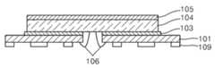
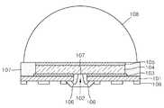
도 1은 본 발명의 일 실시예에 따른 발광소자 패키지(100)의 구조를 개략적으로 보이는 단면도이다. 도 1을 참조하면, 본 발명의 일 실시예에 따른 발광소자 패키지(100)는 개구부(102)를 갖는 배선 기판(101), 배선 기판(101) 위에 배치된 발광소자(104), 상기 개구부(102)를 통해 발광소자(104)의 저면과 배선 기판(101)의 저면 사이를 전기적으로 연결하는 한 쌍의 본딩 와이어(106), 및 발광소자(104)의 상부의 발광면을 제외한 발광소자(104)의 측면을 둘러싸도록 배선 기판(101)의 위에 형성되어 있으며 또한 본딩 와이어(106)를 덮도록 상기 배선 기판(101)의 개구부(102)의 주위에 형성되어 있는 몰딩 부재(107)를 포함할 수 있다. 또한, 발광소자 패키지(100)는 상기 몰딩 부재(107)와 발광소자(104) 위로 배치된, 예를 들어, 반구형 렌즈의 형태를 갖는 투명한 봉지 부재(108)를 더 포함할 수 있다. 또한, 발광소자 패키지(100)는 배선 기판(101)의 저면에 형성된 솔더 레지스트(soler resist)(109)와 솔더 범프(soler bump)(110)를 더 포함할 수 있다.1 is a cross-sectional view schematically showing the structure of a light
발광소자(104)는 예를 들어 발광 다이오드(light emitting diode; LED)와 같은 반도체 발광소자일 수 있다. 도 1에 도시된 바와 같이, 발광소자(104)는 개구부(102)를 덮도록 배선 기판(101) 위에 배치될 수 있다. 이러한 발광소자(104)는 예를 들어 접착층(103)을 이용하여 배선 기판(101) 위에 고정될 수 있다. 또한, 발광소자(104)의 상부 표면 위에는 형광층(105)이 더 도포될 수 있다. 형광층(105)은 발광소자(104)에서 방출되는 광에 의해 여기되어 백색광을 발생시키는 역할을 한다. 이를 위해 형광층(105)은 단수 또는 복수 종의 형광체를 소정의 배합비에 따라 수지 내에 분산시켜 형성될 수 있다. 실리콘 수지 또는 에폭시 수지와 같은 수지 내에 분산된 형광체의 종류 및 배합비는 발광소자(104)의 발광 특성에 따라 선택될 수 있다. 형광층(105)은 발광소자(104)의 상부 표면인 발광면 위에 전체적으로 도포될 수 있다. 그러나, 백색 발광이 요구되지 않는 경우에는 형광층(105)은 생략될 수도 있다.The
도 1에 도시된 발광소자(104)의 경우, 발광소자(104)의 발광면과 반대쪽 면인 발광소자(104)의 저면에 전극 패드(도시되지 않음)가 형성될 수 있다. 따라서, 본딩 와이어(106)의 일측 단부는 발광소자(104)의 저면에 형성된 전극 패드와 연결된다. 본딩 와이어(106)의 타측 단부는 배선 기판(101)의 개구부(102)를 통과하여 배선 기판(101)의 저면에 연결된다. 본딩 와이어(106)와의 전기적 접속을 위하여, 상기 배선 기판(101)의 저면에는 본딩 패드가 형성될 수 있다. 도 1에 도시된 실시예에서, 본딩 와이어(106)가 발광소자(104)의 상부면에 연결되지 않고 저면에 연결되기 때문에, 발광소자(104)의 상부면에는 전극 패드가 형성될 필요가 없다. 따라서 발광소자(104)의 상부면인 발광면의 면적이 상대적으로 증가할 수 있다. 또한, 발광소자(104)의 측면 주의에 와이어 본딩을 위한 추가적인 공간을 마련할 필요가 없기 때문에, 발광소자 패키지(100)의 전체적인 크기를 더 작게 할 수 있다.In the case of the
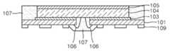
배선 기판(101)은 외부의 전원(도시되지 않음)과 연결되어, 외부의 전원으로부터 본딩 와이어(106)를 통해 발광소자(104)에 전류를 인가하는 역할을 한다. 또한, 배선 기판(101)은 발광소자(104)에서 발생하는 열을 외부로 발산시키는 역할을 할 수 있다. 이를 위하여 배선 기판(101)은 도전성을 갖는 금속 배선을 포함할 수 있다. 예를 들어, 배선 기판(101)은 전체적으로 금속으로 이루어진 리드 프레임 그 자체일 수 있다. 이 경우, 배선 기판(101)은 개구부(102)를 중심으로 양측에 전기적으로 분리되어 각각 배치된 한쌍의 리드 프레임을 포함할 수 있다. 여기서, 개구부(102)는 분리된 두 리드 프레임 사이의 공간일 수 있다. 다른 실시예에서, 배선 기판(101)은 예를 들어 인쇄회로기판(PCB)과 같이, 절연성 수지 기판 및 상기 절연성 수지 기판의 저면에 형성되어 있는 금속 배선 패턴을 포함할 수 있다. 이 경우 절연성 수지 기판의 중심부에는 절연성 수지 기판을 관통하는 개구부(102)가 형성되어 있으며, 개구부(102)의 양측으로 한 쌍의 금속 배선 패턴이 전기적으로 분리되어 각각 형성될 수 있다. 그러면 본딩 와이어(106)는 상기 한 쌍의 리드 프레임 또는 금속 배선 패턴에 각각 연결될 수 있다.The
도 2는 상술한 배선 기판(101) 및 상기 배선 기판(101)의 저면에 형성된 금속 배선 패턴을 예시적으로 보이는 개략적인 저면도이다. 도 2를 참조하면, 배선 기판(101)은 예를 들어 중심부에 개구부(102)를 갖는 절연성 수지 기판(101c) 및 상기 절연성 수지 기판(101c)의 저면에서 개구부(102)의 양측에 각각 형성된 두 개의 금속 배선 패턴(101a, 101b)을 포함할 수 있다. 도 2에는 다수의 발광소자 패키지(100)를 일괄 공정으로 형성하기 위한 다수의 절연성 수지 기판(101c) 및 다수의 금속 배선 패턴(101a, 101b)들의 어레이가 도시되어 있다. 예를 들어 다수의 금속 배선 패턴(101a, 101b)들은 다수의 타이 바(tie bar)(120)를 통해 2차원 매트릭스의 형태로 서로 연결될 수 있다. 또한, 도 2에는 다수의 절연성 수지 기판(101c)이 점선으로 표시되어 있으나, 다수의 절연성 수지 기판(101c)은 실제로는 하나의 큰 기판일 수 있다. 다수의 발광소자 패키지(100)가 완성된 후에는 타이 바(120)가 있는 부분을 절단하여 각각의 발광소자 패키지(100)를 분리할 수 있다. 따라서, 이러한 구조는 발광소자 패키지(100)의 대량 생산에 유리할 수 있다. 만약, 상기 배선 기판(101)이 리드 프레임 그 자체인 경우, 배선 기판(101)은 금속 배선 패턴(101a, 101b)만을 포함할 수도 있다.2 is a schematic bottom view illustrating an example of the
도 2에는 배선 기판(101)의 상면 위에 발광소자(104)가 배치될 영역(104a)이 점선 사각형으로 표시되어 있다. 도 2에 도시된 바와 같이, 개구부(102)는 폭이 좁고 길이가 긴 슬롯의 형태를 갖는다. 예컨대, 개구부(102)의 폭은 발광소자(104)의 폭보다 좁으며, 길이는 발광소자(104)의 폭보다 길다. 따라서, 배선 기판(101) 위에 발광소자(104)가 배치된 뒤에도, 개구부(102)가 발광소자(104)에 의해 막히지 않는다. 이는 이후의 몰딩 부재(107)를 형성하는 공정에서 몰딩 부재(107)의 재료가 개구부(102)를 통해 배선 기판(101)의 상하부 사이를 흐를 수 있도록 하기 위한 것이다.In FIG. 2, a
도 1에 도시된 바와 같이, 배선 기판(101)의 저면에는 솔더 레지스트(109)와 솔더 범프(110)가 더 형성될 수 있다. 솔더 범프(110)는 발광소자 패키지(100)를 사용하는 조명 장치와 같은 다른 장치의 회로 기판 위에 발광소자 패키지(100)가 표면 실장될 수 있도록 한다. 솔더 범프(110)의 형성을 위해, 예를 들어 소정의 패턴을 갖는 솔더 레지스트(109)를 배선 기판(101)의 저면에 먼저 형성할 수 있다. 그런 후에, 솔더 범프(110)는 상기 솔더 레지스트(109)가 형성되어 있지 않은 배선 기판(101)의 저면에 부착될 수 있다.As shown in FIG. 1, a solder resist 109 and a
도 3a 내지 도 3e는 이러한 솔더 범프(110)의 형성을 위한 배선 기판(101)의 다양한 하부 구조들을 개략적으로 보이는 저면도이다. 예를 들어, 도 3a를 참조하면, 배선 기판(101)의 저면에는 솔더 레지스트(109)가 전체적으로 형성되어 있으며, 솔더 레지스트(109)가 형성되어 있지 않은 본딩 패드(116)와 볼 랜드(ball land)(110a)들이 부분적으로 존재한다. 솔더 레지스트(109)가 형성되어 있지 않은 상기 본딩 패드(116)와 볼 랜드(110a)에는, 예를 들어, 배선 기판(101)의 금속 배선 패턴(101a, 101b)이 노출될 수 있다. 개구부(102)의 양측에 형성된 본딩 패드(116)는 본딩 와이어(106)와 금속 배선 패턴(101a, 101b) 사이의 연결을 위한 영역이다. 그리고, 다수의 볼 랜드(110a)는 솔더 범프(110)가 형성될 영역이다. 이와 같이, 본딩 패드(116)와 볼 랜드(110a)의 영역에는 솔더 레지스트(109)가 형성되어 있지 않고 금속 배선 패턴(101a, 101b)이 노출되기 때문에, 본딩 와이어(106)와 솔더 범프(101)가 금속 배선 패턴(101a, 101b)에 부착될 수 있다. 또한, 솔더 레지스트(109)를 사용함으로써 금속 배선 패턴(101a, 101b) 상의 원하는 영역에만 솔더 범프(101)를 형성시킬 수 있다.3A to 3E are bottom views schematically showing various substructures of the
도 3a에는 두 개의 본딩 패드(116)가 개구부(102)의 양측 중앙에 서로 대향하도록 도시되어 있으나, 본 발명은 이에 한정되지 않는다. 예를 들어, 도 3b에 도시된 바와 같이, 두 개의 본딩 패드(116)는 개구부(102)의 양측 반대쪽 가장자리에서 서로 엇갈리에 배치될 수도 있다. 또한, 본딩 패드(116)는 도 3c에 도시된 바와 같이, 개구부(102)를 향해 돌출되어 형성될 수도 있다. 이를 위해, 금속 배선 패턴(101a, 101b)의 일부분이 개구부(102)를 향해 돌출하여 연장되도록 패터닝될 수 있다. 또한, 솔더 레지스트(109)는 개구부(102)를 향해 연장된 금속 배선 패턴(101a, 101b)의 일부분 위에는 형성되지 않는다. 이렇게 개구부(102)를 향해 돌출되어 형성된 본딩 패드(116)는 도 3d에 도시된 바와 같이 다수 개가 존재할 수도 있다. 또한, 도 3e에 도시된 바와 같이, 배선 기판(101)에는 다수의 개구부(102)가 존재할 수도 있으며, 각각의 개구부(102)마다 본딩 패드(116)가 형성될 수 있다. 다수의 개구부(102)가 존재하는 경우, 각각의 개구부(102)의 길이는 발광소자(104)가 배치될 영역(104a)의 폭보다 짧을 수도 있다. 이 경우, 개구부(102)들은 발광소자(104)가 배치될 영역(104a)의 경계를 가로질러 걸쳐 있어서, 발광소자(104)가 배선 기판(101) 위에 부착된 후에도 각각의 개구부(102)들은 부분적으로만 막히게 된다. 한편, 도 3a 내지 도 3e에는 개구부(102)의 주위에 몰딩 부재(107)가 형성될 영역(107a)이 표시되어 있다. 몰딩 부재(107)는 와이어 본딩이 완료된 후 개구부(102) 주위의 상기 영역(107a)에 형성되어 개구부(102)와 본딩 와이어(106)를 완전히 덮을 수 있다.In FIG. 3A, two
도 4a 내지 도 4f는 도 1에 도시된 발광소자 패키지(100)의 제조 방법을 개략적으로 도시하는 단면도이다. 먼저, 도 4a를 참조하면, 중심부에 개구부(102)가 형성되어 있는 배선 기판(101)을 마련하고, 상기 배선 기판(101)의 저면에 소정의 패턴을 갖는 솔더 레지스트(109)를 형성한다. 그런 후, 도 4b에 도시된 바와 같이, 접착층(103)을 이용하여 배선 기판(101) 위에 발광소자(104)를 부착시킨다. 여기서, 발광소자(104)의 상부 표면에는 형광층(105)이 미리 도포되어 있을 수 있다. 그러나, 발광소자(104)를 배선 기판(101) 위에 먼저 부착시킨 후에, 형광층(105)을 발광소자(104)의 상부 표면에 도포하는 것도 가능하다. 만약 발광소자(104)가 자체적으로 백색광을 방출하는 경우에는 형광층(105)이 없을 수도 있다. 또한, 특정한 색의 광을 방출하는 발광소자 패키지(100)를 제조하는 경우에도, 발광소자(104) 위에 형광층(105)이 도포되지 않을 수 있다.4A to 4F are cross-sectional views schematically illustrating a method of manufacturing the light emitting
다음으로, 도 4c에 도시된 바와 같이, 발광소자(104)의 저면과 배선 기판(101)의 저면 사이를 본딩 와이어(106)로 연결한다. 이를 위해, 발광소자(104)의 저면에는 전극 패드(도시되지 않음)가 형성될 수 있으며, 배선 기판(101)의 저면에도 본딩 패드(116, 도 3 참조)가 개구부(102)의 양측으로 형성될 수 있다. 그러면 본딩 와이어(106)는 개구부(102)를 통과하여 상기 발광소자(104)의 전극 패드와 배선 기판(101)의 본딩 패드에 전기적으로 연결될 수 있다.Next, as shown in FIG. 4C, a
그런 후에는, 도 4d에 도시된 바와 같이, 배선 기판(101) 위의 발광소자(104)의 측면을 둘러싸도록 몰딩 부재(107)를 형성한다. 이때, 몰딩 부재(107)는 개구부(102) 주위에도 함께 형성되어 개구부(102)와 본딩 와이어(106)를 덮을 수 있다. 예를 들어, 발광소자(104)가 부착된 배선 기판(101)을 금형틀 내에 배치시키고, 트랜스퍼 몰딩(transfer molding) 방식으로 몰딩 부재(107)를 형성할 수 있다.Thereafter, as shown in FIG. 4D, the
도 5에는 몰딩 부재(107)를 형성하기 위한 트랜스퍼 몰딩 방법이 예시적으로 도시되어 있다. 도 5를 참조하면, 도 4c의 단계까지 진행된 제조 과정 중의 발광소자 패키지를 하부 주형틀(bottom die)(131) 위에 배열한 후, 하부 주형틀(131) 위로 상부 주형틀(132)을 덮어서 하부 주형틀(131)과 상부 주형틀(132) 사이의 몰딩을 위한 공동(cavity)을 완전히 밀폐시킨다. 다만 주형틀(131, 132)의 좌측의 유입구(136)와 우측의 배출구(137)만이 열려 있는 상태가 된다. 이때, 발광소자(104)의 상부 표면은 상부 주형틀(132)의 저면과 완전히 밀착된다. 상부 주형틀(132)의 저면에는 몰딩 필름(133)이 형성되어 있어서, 발광소자(104)의 상부 표면을 보호하고 몰딩 재료(117)가 상부 주형틀(132)의 저면에 달라붙지 않게 한다. 또한, 하부 주형틀(131)과 배선 기판(101)의 사이를 밀폐함으로써, 유입구(136)를 통해 공동에 주입되는 몰딩 재료(117)가 배선 기판(101)의 위쪽으로 흐르도록 한다. 그리고, 배선 기판(101)의 개구부(102)와 대향하는 하부 주형틀(131)의 상면에는 홈(134)이 형성되어 있어서, 개구부(102) 주위에 몰딩 부재(107)가 형성될 공간이 마련된다.5 illustrates an exemplary transfer molding method for forming the
그런 후, 몰딩 재료(117)를 제공하기 위한 폿 블록(pot block)(138)을 유입구(136)에 고정시키고, 플런저(135)로 몰딩 재료(117)를 가압하여 유입구(136)를 통해 공동 내부로 몰딩 재료(117)를 주입한다. 그러면, 몰딩 재료(117)는 배선 기판(101)의 상부로 흘러서 발광소자(104)의 측면을 완전히 채우게 된다. 또한, 몰딩 재료(117)는 개구부(102)를 통해 배선 기판(101)의 아래로 흘러서 개구부(102)와 본딩 와이어(106)의 주위를 완전히 채우게 된다. 용융 상태의 몰딩 재료(117)가 완전히 채워진 후에는 몰딩 재료(117)를 냉각시켜 경화시킨다. 냉각이 완료된 후, 하부 및 상부 주형틀(131, 132)을 제거하면, 도 4d에 도시된 바와 같이 몰딩 부재(107)가 형성될 수 있다.Thereafter, a
이어서, 도 4e에 도시된 바와 같이, 몰딩 부재(107) 위로 투명한 봉지 부재(108)를 형성한다. 봉지 부재(108)는 예를 들어 반구형 렌즈의 형태로 형성될 수 있다. 이러한 봉지 부재(108)는 투명한 실리콘 수지 등으로 이루어질 수 있다. 마지막으로, 도 4f에 도시된 바와 같이, 솔더 레지스트(109)가 형성되어 있지 않은 배선 기판(101)의 저면에 솔더 범프(110)를 형성할 수 있다. 이렇게 함으로써 발광소자 패키지(100)가 완성될 수 있다.Subsequently, as shown in FIG. 4E, a
상술한 바와 같이, 본 발명의 일 실시예에 따른 발광소자 패키지(100)는 발광소자(104)를 배선 기판(101) 위에 먼저 실장한 후, 나중에 몰딩 부재(107)를 형성하는 후몰딩(post-molding) 방식으로 제조될 수 있다. 따라서, 몰딩 부재(107)를 배선 기판(101) 위에 먼저 형성하는 선몰딩 방식에 비하여, 발광소자(104)를 위치시키기 위한 공간이 절약될 수 있다. 이로 인해, 발광소자 패키지(100)의 크기를 더 소형화할 수 있다. 또한, 후몰딩 방식의 경우, 몰딩 부재(107)가 발광소자(104)의 상부 표면을 제외한 측면 전체를 완전히 밀착하여 둘러쌀 수 있다. 따라서, 광반사율이 우수한 몰딩 재료를 사용할 경우, 발광소자(104)의 측면으로 부분적으로 방출되는 광을 몰딩 부재(107)가 반사하여 광의 재활용이 가능하다. 이를 위해, 본 발명의 일 실시예에서, 몰딩 부재(107)는 우수한 광반사율을 갖는 백색 몰딩 재료로 이루어질 수 있다. 예를 들어, 몰딩 부재(107)는 몰딩 수지 내에 TiO2와 같은 재료를 혼합하여 형성될 수 있다. 그러면 발광소자 패키지(100)의 광 방출 효율이 향상될 수 있다. 또한, 발광소자(104)의 측면으로 부분적으로 광이 방출되는 경우에도, 발광소자(104)의 상부 표면에만 형광층(105)을 도포하여도 되므로, 발광소자 패키지(100)의 광 품질의 산포를 줄일 수 있다.As described above, the light emitting
도 6은 본 발명의 다른 실시예에 따른 발광소자 패키지(200)의 구조를 개략적으로 보이는 단면도이다. 도 1의 발광소자 패키지(100)와 비교할 때, 도 6에 도시된 발광소자 패키지(200)의 몰딩 부재(107)는 상부 표면의 높이가 발광소자(104)의 상부 표면의 높이와 일치하도록 형성되어 있다는 점에서 차이가 있다. 도 1에 도시된 발광소자 패키지(100)의 경우, 몰딩 부재(107)는 발광소자(104)의 측면뿐만 아니라 형광층(105)의 측면까지 둘러싸도록, 발광소자(104)보다 높게 형성되어 있다. 반면, 도 6에 도시된 실시예의 경우, 몰딩 부재(107)는 발광소자(104)의 측면만을 둘러싸며 형광층(105)의 측면은 둘러싸지 않는다. 따라서, 발광소자(104) 위에 도포된 형광층(105)은 몰딩 부재(107)의 상부 표면보다 높게 형성되어 있다. 본 실시예의 경우에는, 몰딩 부재(107)의 형성이 먼저 완료된 후에 발광소자(104) 위에 형광층(105)이 형성된다. 그러면 몰딩 부재(107)의 형성 과정에서 발생할 수도 있는 형광층(105)의 손상이나 오염을 방지할 수 있다. 도 6에 도시된 발광소자 패키지(200)의 나머지 구성은 도 1에 도시된 발광소자 패키지(100)에 대해 설명한 것과 동일하다.6 is a cross-sectional view schematically showing the structure of a light emitting
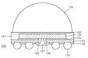
또한, 도 7은 본 발명의 또 다른 실시예에 따른 발광소자 패키지(300)의 구조를 개략적으로 도시하고 있다. 도 7에 도시된 발광소자 패키지(300)의 경우, 배선 기판(101)의 하부에 솔더 레지스트(109) 및 솔더 범프(110)가 형성되어 있지 않다. 대신에 배선 기판(101)은 리드 프레임 그 자체일 수 있다. 이 경우, 리드 프레임이 발광소자(104)와 직접 접촉하므로 열 방출 효과를 향상시킬 수 있다. 또한, 도 1에 도시된 발광소자 패키지(100)의 실시예에서는 개구부(102) 주위의 몰딩 부재(107)가 배선 기판(101)으로부터 돌출되어 있는 반면, 도 7에 도시된 실시예에서는 배선 기판(101)의 개구부(102) 주위에 형성된 몰딩 부재(107)는 배선 기판(101)의 저면과 동일한 높이로 평탄하게 형성되어 있다. 이때, 본딩 와이어(106)가 개구부(102) 주위의 몰딩 부재(107)에 의해 완전히 덮일 수 있도록, 배선 기판(101)은 개구부(102)의 양측에서 단차를 갖도록 형성될 수 있다. 따라서, 개구부(102)의 폭은 발광소자(104)와 가까운 부분에서 상대적으로 좁고, 배선 기판(101)의 저면과 가까운 부분에서 상대적으로 넓어진다.In addition, Figure 7 schematically shows the structure of a light emitting
도 8은 본 발명의 또 다른 실시예에 따른 발광소자 패키지(400)의 구조를 개략적으로 도시하고 있다. 도 7의 실시예와 비교할 때, 도 8에 도시된 실시예의 경우에는 몰딩 부재(107)가 배선 기판(101)의 측면까지 완전히 덮고 있다. 이 경우, 다수의 발광소자 패키지(400)들을 한꺼번에 어레이의 형태로 제조한 후, 이들을 개별적으로 분리하는 과정에서 블레이드와 같은 절단 도구의 수명을 증가시킬 수 있다. 다수의 발광소자 패키지(400)들 사이의 절단면에 금속과 같은 재료가 없고 상대적으로 경도가 낮은 몰딩 부재(107)가 존재하기 때문이다.8 schematically shows the structure of a light emitting
도 9는 본 발명의 또 다른 실시예에 따른 발광소자 패키지(500)의 구조를 개략적으로 도시하고 있다. 도 9에 도시된 발광소자 패키지(500)는 발광소자(104)를 직접 접촉하여 둘러싸는 제 1 몰딩 부재(107) 및 상기 제 1 몰딩 부재(107)를 둘러싸는 제 2 몰딩 부재(127)를 포함할 수 있다. 제 2 몰딩 부재(127)는 또한 본딩 와이어(106)를 둘러싸도록 개구부(102) 주위에도 형성될 수 있다. 여기서, 제 1 몰딩 부재(107)는 백색 몰딩 재료로 이루어지며, 제 2 몰딩 부재(127)는 백색이 아닌 유색 몰딩 재료로 이루어질 수 있다. 유색 몰딩 재료는 백색 몰딩 재료에 비하여 값이 싸고 기계적 물성 및 작업성이 우수하므로, 유색 몰딩 재료를 사용하면 발광소자 패키지(500)의 제조 비용을 절감할 수 있다. 예를 들어, 유색 몰딩 재료로는 반도체 칩의 봉지재로 주로 사용되는 EMC(epoxy molding compound)를 사용할 수 있다. 다만, 발광소자(104)의 측면으로 방출되는 일부의 광을 반사하기 위하여, 백색 몰딩 재료로 이루어진 제 1 몰딩 부재(107)를 발광소자(104)의 측면에 먼저 형성한 후, 나머지 부분에는 제 2 몰딩 부재(127)를 형성할 수 있다. 그러나, 만약 발광소자(104)의 측면으로 전혀 광이 방출되지 않는다면, 유색 몰딩 재료로 이루어진 하나의 몰딩 부재만을 형성할 수도 있다. 예를 들어, 도 1 및 도 6 내지 도 8에 도시된 몰딩 부재(107)는 백색 몰딩 재료가 아닌 유색 몰딩 재료로 이루어질 수 있다.9 schematically illustrates the structure of a light emitting
도 10은 본 발명의 또 다른 실시예에 따른 발광소자 패키지(600)의 구조를 개략적으로 도시하고 있다. 도 10에 도시된 발광소자 패키지(600)의 경우, 전극 패드가 발광소자(104)의 중심부에 모여 있지 않고 양쪽 가장자리에 배치되어 있다. 이에 따라, 배선 기판(101)은 발광소자(104)의 전극 패드에 대응하는 위치에 다수의 개구부(102)를 갖는다. 본딩 와이어(106)는 각각의 개구부(102)를 통해 발광소자(104)와 배선 기판(101)을 전기적으로 연결한다.10 schematically illustrates a structure of a light emitting
마지막으로 도 11은 본 발명의 또 다른 실시예에 따른 발광소자 패키지(700)의 구조를 개략적으로 도시하고 있다. 도 11에 도시된 발광소자 패키지(700)는 다수의 발광소자(104)들을 가지며, 각의각 발광소자(104)들을 배선 기판(101)과 전기적으로 연결시키기 위하여 다수 쌍의 본딩 와이어(106) 및 다수의 개구부(102)를 가질 수 있다. 본 실시예에 따르면, 하나의 발광소자 패키지(700) 내에 다수의 발광소자(104)들이 배치되기 때문에, 발광소자 패키지(700)의 휘도를 향상시킬 수 있다.Finally, FIG. 11 schematically shows the structure of a light emitting
지금까지, 본 발명의 이해를 돕기 위하여 발광소자 패키지 및 그 제조 방법에 대한 예시적인 실시예가 설명되고 첨부된 도면에 도시되었다. 그러나, 이러한 실시예는 단지 본 발명을 예시하기 위한 것이고 이를 제한하지 않는다는 점이 이해되어야 할 것이다. 그리고 본 발명은 도시되고 설명된 설명에 국한되지 않는다는 점이 이해되어야 할 것이다. 이는 다양한 다른 변형이 본 기술분야에서 통상의 지식을 가진 자에게 일어날 수 있기 때문이다.Thus far, exemplary embodiments of a light emitting device package and a method of manufacturing the same have been described and illustrated in the accompanying drawings in order to facilitate understanding of the present invention. However, it should be understood that such embodiments are merely illustrative of the invention and do not limit it. And it is to be understood that the invention is not limited to the details shown and described. This is because various other modifications may occur to those skilled in the art.
100, 200, 300, 400, 500, 600, 700.....발광소자 패키지
101.....배선 기판102.....개구부
103.....접착층104.....발광소자
105.....형광층106.....본딩 와이어
107, 127.....몰딩 부재108.....봉지 부재
109.....솔더 레지스트110.....솔더 범프
116.....본딩 패드117.....몰딩 재료
120.....타이 바(tie bar)131,132.....주형틀(die)
133.....몰딩 필름135.....플런저(plunger)100, 200, 300, 400, 500, 600, 700 ..... LED package
101 ..... wiring
103 .....
105 .....
107, 127 .....
109 ..... solder resist 110 ..... solder bump
116 .....
120 ..... tie bar 131,132 ..... die
133 .....
Claims (23)
Translated fromKorean상기 개구부를 덮도록 상기 배선 기판 위에 배치된 발광소자;
상기 개구부를 통하여 상기 배선 기판의 저면과 상기 발광소자의 저면 사이를 전기적으로 연결하는 본딩 와이어; 및
상기 발광소자의 발광면인 상부 표면을 제외한 상기 발광소자의 측면을 둘러싸도록 상기 배선 기판의 상면에 형성되어 있으며, 또한 상기 본딩 와이어를 덮도록 상기 배선 기판의 개구부 주위에 형성되어 있는 몰딩 부재;를 포함하는 발광소자 패키지.A wiring board having an opening;
A light emitting element disposed on the wiring substrate to cover the opening;
A bonding wire electrically connecting the bottom surface of the wiring board and the bottom surface of the light emitting device through the opening; And
A molding member formed on an upper surface of the wiring board so as to surround a side surface of the light emitting device except for an upper surface which is a light emitting surface of the light emitting device, and formed around an opening of the wiring board to cover the bonding wire; Light emitting device package comprising.
상기 배선 기판은 상기 개구부를 중심으로 양측에 전기적으로 분리되어 각각 배치된 한쌍의 리드 프레임이며, 상기 개구부는 상기 분리된 리드 프레임들 사이의 공간인 발광소자 패키지.The method of claim 1,
The wiring board is a pair of lead frames that are electrically separated on both sides of the opening, respectively, and are disposed, and the opening is a space between the separated lead frames.
상기 개구부 주위에 형성된 몰딩 부재는 상기 배선 기판의 저면과 동일한 높이로 평탄하게 형성되어 있는 발광소자 패키지.The method of claim 2,
The molding member package formed around the opening is formed to be flat to the same height as the bottom surface of the wiring board.
상기 개구부의 폭이 상기 발광소자와 가까운 부분에서 상대적으로 좁고 상기 배선 기판의 저면과 가까운 부분에서 상대적으로 넓어지도록, 상기 배선 기판은 상기 개구부의 양측에 단차를 갖는 발광소자 패키지.The method of claim 3, wherein
And the wiring board has steps on both sides of the opening such that the width of the opening is relatively narrow at the portion close to the light emitting element and relatively wide at the portion close to the bottom surface of the wiring substrate.
상기 배선 기판은 상기 개구부를 갖는 절연성 수지 기판 및 상기 개구부의 양측으로 전기적으로 분리되어 상기 절연성 수지 기판의 저면에 배치된 한 쌍의 금속 배선 패턴을 포함하는 발광소자 패키지.The method of claim 1,
The wiring board includes an insulating resin substrate having the opening and a pair of metal wiring patterns electrically separated from both sides of the opening and disposed on a bottom surface of the insulating resin substrate.
상기 배선 기판의 저면에 소정의 패턴을 갖도록 형성된 솔더 레지스트 및 상기 솔더 레지스트 사이에서 상기 배선 기판의 저면에 형성된 솔더 범프를 더 포함하는 발광소자 패키지.The method of claim 1,
And a solder bump formed on the bottom surface of the wiring board between the solder resist formed to have a predetermined pattern on the bottom surface of the wiring board and the solder resist.
상기 개구부는 상기 발광소자의 폭보다 좁은 폭을 가지며, 상기 발광소자의 폭보다 긴 길이를 갖는 발광소자 패키지.The method of claim 1,
The opening has a width narrower than the width of the light emitting device, the light emitting device package having a length longer than the width of the light emitting device.
상기 발광소자의 발광면 위에 형성된 형광층을 더 포함하는 발광소자 패키지.The method of claim 1,
Light emitting device package further comprising a fluorescent layer formed on the light emitting surface of the light emitting device.
상기 몰딩 부재는 상기 형광층의 측면을 둘러싸도록 형성된 발광소자 패키지.The method of claim 8,
The molding member package is formed so as to surround the side of the fluorescent layer.
상기 몰딩 부재는 상부 표면의 높이가 상기 발광소자의 상부 표면의 높이와 일치하도록 형성되어 있으며, 상기 발광소자 위의 형광층은 상기 몰딩 부재의 상부 표면보다 높게 형성되어 있는 발광소자 패키지.The method of claim 8,
The molding member has a height of the upper surface is formed to match the height of the upper surface of the light emitting device, and the fluorescent layer on the light emitting device is formed higher than the upper surface of the molding member.
상기 몰딩 부재와 발광소자 위로 배치된 렌즈 형태의 투명한 봉지 부재를 더 포함하는 발광소자 패키지.The method of claim 1,
The light emitting device package further comprises a transparent sealing member in the form of a lens disposed on the molding member and the light emitting device.
상기 몰딩 부재는 상기 배선 기판의 측면까지 덮도록 형성되어 있는 발광소자 패키지.The method of claim 1,
The molding member package is formed so as to cover the side of the wiring board.
상기 몰딩 부재는 백색 또는 유색 몰딩 재료로 이루어지는 발광소자 패키지.The method of claim 1,
The molding member is a light emitting device package made of a white or colored molding material.
상기 몰딩 부재는 상기 발광소자의 측면을 직접 접촉하여 둘러싸는 제 1 몰딩 부재, 및 상기 제 1 몰딩 부재를 둘러싸도록 상기 배선 기판 위에 형성되어 있으며 또한 상기 본딩 와이어를 둘러싸도록 상기 개구부 주위에 형성되어 있는 제 2 몰딩 부재를 포함하는 발광소자 패키지.The method of claim 1,
The molding member is formed on the wiring substrate so as to surround the first molding member and the first molding member which directly contacts and surrounds the side surface of the light emitting element, and is formed around the opening to surround the bonding wire. A light emitting device package comprising a second molding member.
상기 제 1 몰딩 부재는 백색 몰딩 재료로 이루어지며, 상기 제 2 몰딩 재료는 유색 몰딩 재료로 이루어지는 발광소자 패키지.15. The method of claim 14,
The first molding member is made of a white molding material, the second molding material is a light emitting device package made of a colored molding material.
상기 배선 기판은 다수의 개구부를 가지며, 상기 본딩 와이어는 각각의 개구부를 통해 상기 발광소자와 배선 기판을 전기적으로 연결하는 발광소자 패키지.The method of claim 1,
The wiring board has a plurality of openings, and the bonding wire electrically connects the light emitting device and the wiring board through each opening.
각각의 개구부의 길이는 상기 발광소자의 폭보다 짧으며, 상기 다수의 개구부들은 상기 발광소자의 경계를 가로질러 걸쳐 있도록 형성되는 발광소자 패키지.17. The method of claim 16,
The length of each opening is shorter than the width of the light emitting device, wherein the plurality of openings are formed so as to cross the boundary of the light emitting device.
상기 배선 기판 위에 상기 개구부를 덮도록 발광소자를 배치하는 단계;
상기 개구부를 통해 상기 발광소자의 저면과 상기 배선 기판의 저면 사이에 본딩 와이어를 연결하는 단계; 및
상기 발광소자의 발광면인 상부 표면을 제외한 상기 발광소자의 측면을 둘러싸도록 상기 배선 기판의 상면에 몰딩 부재를 형성하는 동시에, 상기 본딩 와이어를 덮도록 상기 배선 기판의 개구부 주위에 몰딩 부재를 형성하는 단계;를 포함하는 발광소자 패키지의 제조 방법.Disposing a wiring board having an opening;
Disposing a light emitting device on the wiring substrate to cover the opening;
Connecting a bonding wire between the bottom of the light emitting device and the bottom of the wiring board through the opening; And
Forming a molding member on an upper surface of the wiring board so as to surround a side surface of the light emitting device except for an upper surface which is a light emitting surface of the light emitting device, and forming a molding member around an opening of the wiring board to cover the bonding wire. Method of manufacturing a light emitting device package comprising a.
상기 몰딩 부재를 형성하는 단계는, 상기 발광소자가 부착된 상기 배선 기판을 금형틀 내에 배치시킨 후 트랜스퍼 몰딩(transfer molding) 방식으로 몰딩 부재를 형성하는 것을 포함하는 발광소자 패키지의 제조 방법.The method of claim 18,
The forming of the molding member may include forming the molding member by a transfer molding method after disposing the wiring board to which the light emitting device is attached in a mold.
상기 몰딩 부재를 형성하는 단계는:
상기 발광소자가 부착된 상기 배선 기판을 하부 주형틀 위에 배열하는 단계;
상기 하부 주형틀 위로 상부 주형틀을 덮어서, 유입구와 배출구를 제외한 상기 하부 주형틀과 상부 주형틀 사이의 공동을 밀폐시키는 단계;
상기 유입구를 통해 공동 내에 몰딩 재료를 주입하는 단계; 및
상기 몰딩 재료를 냉각시킨 후, 상기 하부 및 상부 주형틀을 제거하는 단계를 포함하는 발광소자 패키지의 제조 방법.The method of claim 19,
Forming the molding member is:
Arranging the wiring board to which the light emitting element is attached on a lower mold;
Covering the upper mold over the lower mold to seal a cavity between the lower mold and the upper mold except for an inlet and an outlet;
Injecting molding material into the cavity through the inlet; And
After cooling the molding material, removing the lower and upper molds.
상기 발광소자의 상부 표면은 상기 상부 주형틀의 저면과 밀착되어 있으며, 상기 하부 주형틀과 배선 기판의 사이를 밀폐함으로써, 상기 유입구를 통해 주입되는 몰딩 재료가 상기 배선 기판의 상부로 흐르도록 하는 발광소자 패키지의 제조 방법.21. The method of claim 20,
The upper surface of the light emitting device is in close contact with the bottom surface of the upper mold, and the sealing between the lower mold and the wiring board, the light emitting to flow the molding material injected through the inlet to the upper portion of the wiring board Method of manufacturing device package.
상기 개구부는 상기 발광소자의 폭보다 좁은 폭을 가지며 상기 발광소자의 폭보다 긴 길이를 갖고, 상기 몰딩 재료는 상기 개구부를 통해 상기 배선 기판의 아래로 흘러서 상기 본딩 와이어를 덮도록 상기 개구부 주위를 채우는 발광소자 패키지의 제조 방법.22. The method of claim 21,
The opening has a width narrower than the width of the light emitting device and has a length longer than the width of the light emitting device, wherein the molding material flows down the wiring substrate through the opening and fills around the opening to cover the bonding wire. Method of manufacturing a light emitting device package.
상기 개구부 주위에 몰딩 부재가 형성될 공간이 마련될 수 있도록, 상기 배선 기판의 개구부와 대향하는 상기 하부 주형틀의 상면에 홈이 형성되어 있는 발광소자 패키지의 제조 방법.The method of claim 22,
And a groove formed on an upper surface of the lower mold frame facing the opening of the wiring board so that a space for forming the molding member may be provided around the opening.
Priority Applications (4)
| Application Number | Priority Date | Filing Date | Title |
|---|---|---|---|
| KR1020110005985AKR101766299B1 (en) | 2011-01-20 | 2011-01-20 | Light emitting device package and method of manufacturing the light emitting device package |
| US13/348,369US8952404B2 (en) | 2011-01-20 | 2012-01-11 | Light-emitting device package and method of manufacturing the light-emitting device package |
| EP12151738.7AEP2479810B1 (en) | 2011-01-20 | 2012-01-19 | Light-emitting device package and method of manufacturing the same |
| CN201210019906.9ACN102610599B (en) | 2011-01-20 | 2012-01-20 | Light emitting device packaging piece and manufacture method thereof |
Applications Claiming Priority (1)
| Application Number | Priority Date | Filing Date | Title |
|---|---|---|---|
| KR1020110005985AKR101766299B1 (en) | 2011-01-20 | 2011-01-20 | Light emitting device package and method of manufacturing the light emitting device package |
Publications (2)
| Publication Number | Publication Date |
|---|---|
| KR20120084554Atrue KR20120084554A (en) | 2012-07-30 |
| KR101766299B1 KR101766299B1 (en) | 2017-08-08 |
Family
ID=45491468
Family Applications (1)
| Application Number | Title | Priority Date | Filing Date |
|---|---|---|---|
| KR1020110005985AExpired - Fee RelatedKR101766299B1 (en) | 2011-01-20 | 2011-01-20 | Light emitting device package and method of manufacturing the light emitting device package |
Country Status (4)
| Country | Link |
|---|---|
| US (1) | US8952404B2 (en) |
| EP (1) | EP2479810B1 (en) |
| KR (1) | KR101766299B1 (en) |
| CN (1) | CN102610599B (en) |
Cited By (1)
| Publication number | Priority date | Publication date | Assignee | Title |
|---|---|---|---|---|
| KR20160088674A (en)* | 2015-01-16 | 2016-07-26 | 이우필 | Reflector, and manufacturing method for same |
Families Citing this family (13)
| Publication number | Priority date | Publication date | Assignee | Title |
|---|---|---|---|---|
| KR20120062302A (en)* | 2010-12-06 | 2012-06-14 | 삼성엘이디 주식회사 | Light emitting device package and method of manufacturing the same |
| US10074779B2 (en)* | 2011-03-11 | 2018-09-11 | Seoul Semiconductor Co., Ltd. | LED module, method for manufacturing the same, and LED channel letter including the same |
| DE102011078906A1 (en)* | 2011-07-11 | 2013-01-17 | Osram Opto Semiconductors Gmbh | METHOD FOR PRODUCING AN OPTOELECTRONIC SEMICONDUCTOR COMPONENT BY MEANS OF SPRAYING |
| CN104103748B (en)* | 2013-04-10 | 2016-12-07 | 重庆市路迪机械厂 | Package structure for LED and manufacture method thereof |
| DE102013106689B4 (en)* | 2013-06-26 | 2022-02-03 | OSRAM Opto Semiconductors Gesellschaft mit beschränkter Haftung | Optoelectronic semiconductor component |
| JP6608359B2 (en)* | 2013-07-19 | 2019-11-20 | ルミレッズ ホールディング ベーフェー | PCLED with optical element without substrate carrier |
| CN104701446A (en)* | 2013-12-04 | 2015-06-10 | 展晶科技(深圳)有限公司 | Light emitting diode packaging body manufacturing method |
| DE102014103034A1 (en)* | 2014-03-07 | 2015-09-10 | Osram Opto Semiconductors Gmbh | Optoelectronic component and method for its production |
| EP3370938B1 (en)* | 2015-11-06 | 2020-05-27 | Tactotek Oy | Multilayer structure and related method of manufacturing |
| CN106252471B (en)* | 2016-08-31 | 2019-09-06 | 珠海市一芯半导体科技有限公司 | A multi-I/O flip-chip LED chip array bump packaging structure and packaging method thereof |
| US12002907B2 (en)* | 2018-09-28 | 2024-06-04 | Nichia Corporation | Light emitting module and method for manufacturing same |
| CN109952641B (en)* | 2019-01-15 | 2023-01-10 | 泉州三安半导体科技有限公司 | Light emitting diode package device and light emitting apparatus |
| US12021017B2 (en)* | 2021-10-01 | 2024-06-25 | Nanya Technology Corporation | Semiconductor package and manufacturing method thereof |
Family Cites Families (20)
| Publication number | Priority date | Publication date | Assignee | Title |
|---|---|---|---|---|
| JPH05138691A (en) | 1991-07-19 | 1993-06-08 | Toshiba Chem Corp | Mold for injection molding of liquid resin |
| US5286679A (en)* | 1993-03-18 | 1994-02-15 | Micron Technology, Inc. | Method for attaching a semiconductor die to a leadframe using a patterned adhesive layer |
| EP0632511A3 (en) | 1993-06-29 | 1996-11-27 | Mitsubishi Cable Ind Ltd | Light emitting diode module and method for its manufacture. |
| JPH09312374A (en)* | 1996-05-24 | 1997-12-02 | Sony Corp | Semiconductor package and manufacture thereof |
| DE19901918A1 (en) | 1998-01-28 | 1999-07-29 | Rohm Co Ltd | Light emitting semiconductor device e.g. an LED component |
| US6734465B1 (en)* | 2001-11-19 | 2004-05-11 | Nanocrystals Technology Lp | Nanocrystalline based phosphors and photonic structures for solid state lighting |
| US7264378B2 (en)* | 2002-09-04 | 2007-09-04 | Cree, Inc. | Power surface mount light emitting die package |
| US6835960B2 (en)* | 2003-03-03 | 2004-12-28 | Opto Tech Corporation | Light emitting diode package structure |
| CN101789482B (en)* | 2003-03-10 | 2013-04-17 | 丰田合成株式会社 | Solid element device and method for manufacture thereof |
| DE102004021233A1 (en) | 2004-04-30 | 2005-12-01 | Osram Opto Semiconductors Gmbh | LED array |
| TWI277223B (en) | 2004-11-03 | 2007-03-21 | Chen-Lun Hsingchen | A low thermal resistance LED package |
| JP5219331B2 (en)* | 2005-09-13 | 2013-06-26 | 株式会社住田光学ガラス | Method for manufacturing solid element device |
| KR100726969B1 (en) | 2005-11-28 | 2007-06-14 | 한국광기술원 | Light-Emitting Diode Package with High Heat-Dissipation Board without Submount |
| US7662672B2 (en)* | 2006-10-13 | 2010-02-16 | Chipmos Technologies (Bermuda) Ltd. | Manufacturing process of leadframe-based BGA packages |
| JP2008251644A (en)* | 2007-03-29 | 2008-10-16 | Sharp Corp | Semiconductor light emitting device |
| KR100967965B1 (en) | 2008-03-25 | 2010-07-07 | 삼성전기주식회사 | Manufacturing method of light emitting diode package |
| KR101468961B1 (en) | 2008-08-29 | 2014-12-05 | 삼성전자주식회사 | Light emitting device and backlight unit having the same |
| KR101521260B1 (en) | 2008-11-25 | 2015-05-18 | 삼성전자주식회사 | Light emitting diode package and manufacturing method thereof |
| CN102194985B (en)* | 2010-03-04 | 2013-11-06 | 展晶科技(深圳)有限公司 | Wafer level package method |
| KR20120062302A (en) | 2010-12-06 | 2012-06-14 | 삼성엘이디 주식회사 | Light emitting device package and method of manufacturing the same |
- 2011
- 2011-01-20KRKR1020110005985Apatent/KR101766299B1/ennot_activeExpired - Fee Related
- 2012
- 2012-01-11USUS13/348,369patent/US8952404B2/ennot_activeExpired - Fee Related
- 2012-01-19EPEP12151738.7Apatent/EP2479810B1/ennot_activeNot-in-force
- 2012-01-20CNCN201210019906.9Apatent/CN102610599B/ennot_activeExpired - Fee Related
Cited By (1)
| Publication number | Priority date | Publication date | Assignee | Title |
|---|---|---|---|---|
| KR20160088674A (en)* | 2015-01-16 | 2016-07-26 | 이우필 | Reflector, and manufacturing method for same |
Also Published As
| Publication number | Publication date |
|---|---|
| EP2479810A2 (en) | 2012-07-25 |
| CN102610599B (en) | 2016-10-26 |
| EP2479810B1 (en) | 2017-04-19 |
| KR101766299B1 (en) | 2017-08-08 |
| EP2479810A3 (en) | 2012-11-07 |
| US8952404B2 (en) | 2015-02-10 |
| US20120187437A1 (en) | 2012-07-26 |
| CN102610599A (en) | 2012-07-25 |
Similar Documents
| Publication | Publication Date | Title |
|---|---|---|
| KR101766299B1 (en) | Light emitting device package and method of manufacturing the light emitting device package | |
| TWI441350B (en) | Resin-filled illuminator and method of manufacturing same | |
| US8324646B2 (en) | Chip coated light emitting diode package and manufacturing method thereof | |
| KR101488448B1 (en) | LED package and manufacturing method thereof | |
| CN101222010B (en) | Photoelectric component packaging structure and packaging method | |
| CN100570913C (en) | Manufacturing method of light emitting diode | |
| KR200373718Y1 (en) | High Brightness LED With Protective Function of Electrostatic Damage | |
| CN101114689A (en) | Semiconductor light emitting device and manufacturing method thereof | |
| CN102593336A (en) | Light-emitting device package and method of manufacturing the same | |
| WO2012163086A1 (en) | Submount with cavities and through vias for led packaging | |
| KR20120119395A (en) | Light emitting device package and method of manufacturing the same | |
| KR20120094279A (en) | Light emitting device package and method of fabricating the same | |
| KR20090104577A (en) | Multichip LED Package | |
| KR20120094280A (en) | Light emitting device package and method of fabricating the same | |
| KR20120084553A (en) | Package of light emitting device and method of manufacturing the same and lead frame | |
| KR20120085085A (en) | Cob type light emitting module and method of the light emitting module | |
| KR20120083080A (en) | Light emitting device package and method of manufacturing the light emitting device package | |
| CN101226975A (en) | High-power light-emitting diode chip packaging structure and manufacturing method | |
| KR20150042954A (en) | Side-view light emitting device and method of making the same | |
| KR100878398B1 (en) | High output LED package and manufacturing method | |
| CN118431218A (en) | Package structure of semiconductor device and method for manufacturing the same | |
| KR101423455B1 (en) | Led package and method for fabricating the same | |
| CN118431219A (en) | Semiconductor device packaging structure and manufacturing method thereof | |
| KR20120095651A (en) | Light emitting device package and method of manufacturing the same | |
| KR20130091102A (en) | Led package and manufacturing method for the same |
Legal Events
| Date | Code | Title | Description |
|---|---|---|---|
| PA0109 | Patent application | St.27 status event code:A-0-1-A10-A12-nap-PA0109 | |
| R18-X000 | Changes to party contact information recorded | St.27 status event code:A-3-3-R10-R18-oth-X000 | |
| PG1501 | Laying open of application | St.27 status event code:A-1-1-Q10-Q12-nap-PG1501 | |
| N231 | Notification of change of applicant | ||
| PN2301 | Change of applicant | St.27 status event code:A-3-3-R10-R13-asn-PN2301 St.27 status event code:A-3-3-R10-R11-asn-PN2301 | |
| A201 | Request for examination | ||
| E13-X000 | Pre-grant limitation requested | St.27 status event code:A-2-3-E10-E13-lim-X000 | |
| P11-X000 | Amendment of application requested | St.27 status event code:A-2-2-P10-P11-nap-X000 | |
| P13-X000 | Application amended | St.27 status event code:A-2-2-P10-P13-nap-X000 | |
| PA0201 | Request for examination | St.27 status event code:A-1-2-D10-D11-exm-PA0201 | |
| P22-X000 | Classification modified | St.27 status event code:A-2-2-P10-P22-nap-X000 | |
| P22-X000 | Classification modified | St.27 status event code:A-2-2-P10-P22-nap-X000 | |
| E902 | Notification of reason for refusal | ||
| PE0902 | Notice of grounds for rejection | St.27 status event code:A-1-2-D10-D21-exm-PE0902 | |
| E13-X000 | Pre-grant limitation requested | St.27 status event code:A-2-3-E10-E13-lim-X000 | |
| P11-X000 | Amendment of application requested | St.27 status event code:A-2-2-P10-P11-nap-X000 | |
| P13-X000 | Application amended | St.27 status event code:A-2-2-P10-P13-nap-X000 | |
| E701 | Decision to grant or registration of patent right | ||
| PE0701 | Decision of registration | St.27 status event code:A-1-2-D10-D22-exm-PE0701 | |
| GRNT | Written decision to grant | ||
| PR0701 | Registration of establishment | St.27 status event code:A-2-4-F10-F11-exm-PR0701 | |
| PR1002 | Payment of registration fee | St.27 status event code:A-2-2-U10-U11-oth-PR1002 Fee payment year number:1 | |
| PG1601 | Publication of registration | St.27 status event code:A-4-4-Q10-Q13-nap-PG1601 | |
| PR1001 | Payment of annual fee | St.27 status event code:A-4-4-U10-U11-oth-PR1001 Fee payment year number:4 | |
| PR1001 | Payment of annual fee | St.27 status event code:A-4-4-U10-U11-oth-PR1001 Fee payment year number:5 | |
| PC1903 | Unpaid annual fee | St.27 status event code:A-4-4-U10-U13-oth-PC1903 Not in force date:20220803 Payment event data comment text:Termination Category : DEFAULT_OF_REGISTRATION_FEE | |
| PC1903 | Unpaid annual fee | St.27 status event code:N-4-6-H10-H13-oth-PC1903 Ip right cessation event data comment text:Termination Category : DEFAULT_OF_REGISTRATION_FEE Not in force date:20220803 | |
| P22-X000 | Classification modified | St.27 status event code:A-4-4-P10-P22-nap-X000 |