KR20120080908A - Apparatus for controlling bleed switch, power supply, and method for driving power supply - Google Patents
Apparatus for controlling bleed switch, power supply, and method for driving power supplyDownload PDFInfo
- Publication number
- KR20120080908A KR20120080908AKR1020110002378AKR20110002378AKR20120080908AKR 20120080908 AKR20120080908 AKR 20120080908AKR 1020110002378 AKR1020110002378 AKR 1020110002378AKR 20110002378 AKR20110002378 AKR 20110002378AKR 20120080908 AKR20120080908 AKR 20120080908A
- Authority
- KR
- South Korea
- Prior art keywords
- switch
- time interval
- signal
- level
- current
- Prior art date
- Legal status (The legal status is an assumption and is not a legal conclusion. Google has not performed a legal analysis and makes no representation as to the accuracy of the status listed.)
- Withdrawn
Links
- 238000000034methodMethods0.000titleclaimsdescription23
- 238000005070samplingMethods0.000claimsdescription44
- 239000003990capacitorSubstances0.000description27
- 238000010586diagramMethods0.000description16
- 230000000630rising effectEffects0.000description4
- 230000007423decreaseEffects0.000description3
- 230000001960triggered effectEffects0.000description2
- 241000270730Alligator mississippiensisSpecies0.000description1
- 230000003139buffering effectEffects0.000description1
- 230000001934delayEffects0.000description1
- 238000001914filtrationMethods0.000description1
Images


Classifications
- H—ELECTRICITY
- H02—GENERATION; CONVERSION OR DISTRIBUTION OF ELECTRIC POWER
- H02M—APPARATUS FOR CONVERSION BETWEEN AC AND AC, BETWEEN AC AND DC, OR BETWEEN DC AND DC, AND FOR USE WITH MAINS OR SIMILAR POWER SUPPLY SYSTEMS; CONVERSION OF DC OR AC INPUT POWER INTO SURGE OUTPUT POWER; CONTROL OR REGULATION THEREOF
- H02M5/00—Conversion of AC power input into AC power output, e.g. for change of voltage, for change of frequency, for change of number of phases
- H02M5/02—Conversion of AC power input into AC power output, e.g. for change of voltage, for change of frequency, for change of number of phases without intermediate conversion into DC
- H02M5/04—Conversion of AC power input into AC power output, e.g. for change of voltage, for change of frequency, for change of number of phases without intermediate conversion into DC by static converters
- H02M5/22—Conversion of AC power input into AC power output, e.g. for change of voltage, for change of frequency, for change of number of phases without intermediate conversion into DC by static converters using discharge tubes with control electrode or semiconductor devices with control electrode
- H02M5/25—Conversion of AC power input into AC power output, e.g. for change of voltage, for change of frequency, for change of number of phases without intermediate conversion into DC by static converters using discharge tubes with control electrode or semiconductor devices with control electrode using devices of a thyratron or thyristor type requiring extinguishing means
- H02M5/257—Conversion of AC power input into AC power output, e.g. for change of voltage, for change of frequency, for change of number of phases without intermediate conversion into DC by static converters using discharge tubes with control electrode or semiconductor devices with control electrode using devices of a thyratron or thyristor type requiring extinguishing means using semiconductor devices only
- H02M5/2573—Conversion of AC power input into AC power output, e.g. for change of voltage, for change of frequency, for change of number of phases without intermediate conversion into DC by static converters using discharge tubes with control electrode or semiconductor devices with control electrode using devices of a thyratron or thyristor type requiring extinguishing means using semiconductor devices only with control circuit
- H—ELECTRICITY
- H02—GENERATION; CONVERSION OR DISTRIBUTION OF ELECTRIC POWER
- H02M—APPARATUS FOR CONVERSION BETWEEN AC AND AC, BETWEEN AC AND DC, OR BETWEEN DC AND DC, AND FOR USE WITH MAINS OR SIMILAR POWER SUPPLY SYSTEMS; CONVERSION OF DC OR AC INPUT POWER INTO SURGE OUTPUT POWER; CONTROL OR REGULATION THEREOF
- H02M5/00—Conversion of AC power input into AC power output, e.g. for change of voltage, for change of frequency, for change of number of phases
- H02M5/02—Conversion of AC power input into AC power output, e.g. for change of voltage, for change of frequency, for change of number of phases without intermediate conversion into DC
- H02M5/04—Conversion of AC power input into AC power output, e.g. for change of voltage, for change of frequency, for change of number of phases without intermediate conversion into DC by static converters
- H02M5/22—Conversion of AC power input into AC power output, e.g. for change of voltage, for change of frequency, for change of number of phases without intermediate conversion into DC by static converters using discharge tubes with control electrode or semiconductor devices with control electrode
- H02M5/275—Conversion of AC power input into AC power output, e.g. for change of voltage, for change of frequency, for change of number of phases without intermediate conversion into DC by static converters using discharge tubes with control electrode or semiconductor devices with control electrode using devices of a triode or transistor type requiring continuous application of a control signal
- H02M5/293—Conversion of AC power input into AC power output, e.g. for change of voltage, for change of frequency, for change of number of phases without intermediate conversion into DC by static converters using discharge tubes with control electrode or semiconductor devices with control electrode using devices of a triode or transistor type requiring continuous application of a control signal using semiconductor devices only
- H—ELECTRICITY
- H05—ELECTRIC TECHNIQUES NOT OTHERWISE PROVIDED FOR
- H05B—ELECTRIC HEATING; ELECTRIC LIGHT SOURCES NOT OTHERWISE PROVIDED FOR; CIRCUIT ARRANGEMENTS FOR ELECTRIC LIGHT SOURCES, IN GENERAL
- H05B45/00—Circuit arrangements for operating light-emitting diodes [LED]
- H05B45/30—Driver circuits
- H05B45/357—Driver circuits specially adapted for retrofit LED light sources
- H05B45/3574—Emulating the electrical or functional characteristics of incandescent lamps
- H05B45/3575—Emulating the electrical or functional characteristics of incandescent lamps by means of dummy loads or bleeder circuits, e.g. for dimmers
- Y—GENERAL TAGGING OF NEW TECHNOLOGICAL DEVELOPMENTS; GENERAL TAGGING OF CROSS-SECTIONAL TECHNOLOGIES SPANNING OVER SEVERAL SECTIONS OF THE IPC; TECHNICAL SUBJECTS COVERED BY FORMER USPC CROSS-REFERENCE ART COLLECTIONS [XRACs] AND DIGESTS
- Y02—TECHNOLOGIES OR APPLICATIONS FOR MITIGATION OR ADAPTATION AGAINST CLIMATE CHANGE
- Y02B—CLIMATE CHANGE MITIGATION TECHNOLOGIES RELATED TO BUILDINGS, e.g. HOUSING, HOUSE APPLIANCES OR RELATED END-USER APPLICATIONS
- Y02B20/00—Energy efficient lighting technologies, e.g. halogen lamps or gas discharge lamps
- Y02B20/30—Semiconductor lamps, e.g. solid state lamps [SSL] light emitting diodes [LED] or organic LED [OLED]
Landscapes
- Engineering & Computer Science (AREA)
- Power Engineering (AREA)
- Circuit Arrangement For Electric Light Sources In General (AREA)
Abstract
Translated fromKorean
Description
Translated fromKorean본 발명은 전원 장치에 관한 것이다. 특히 본 발명은 트라이액 딤머(TRIAC dimmer)로 제어되는 LED 조명을 위한 블리드 스위치를 포함하는 전원 장치에 관한 것이다.The present invention relates to a power supply device. In particular, the present invention relates to a power supply comprising a bleed switch for an LED light controlled by a triac dimmer.
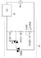
로드에 제공되는 전류의 양을 조절하기 위하여 트라이액 딤머가 널리 사용된다. 트라이액 딤머에 대해 도 1 및 도 2를 참고하여 설명한다.Triac dimmers are widely used to control the amount of current provided to the load. The triac dimmer will be described with reference to FIGS. 1 and 2.
도 1은 종래의 트라이액 딤머를 포함하는 회로도를 보여주고, 도 2는 트라이액 딤머의 동작을 보여주는 파형도이다.Figure 1 shows a circuit diagram comprising a conventional triac dimmer, Figure 2 is a waveform diagram showing the operation of the triac dimmer.
도 1에 도시된 바와 같이, 트라이액 딤머(10)는 교류 전원(Vac) 및 로드(20)와 직렬로 연결된다. 트라이액 딤머(10)는 가변 저항(R1), 저항(R2), 커패시터(C1), 다이액(DIAC), 트라이액(TRIAC)을 포함한다.As shown in FIG. 1, the
교류 전원(Vac)는 도 2의 (A)에 도시된 바와 같은 교류파형의 전압 소스를 제공한다. 가변 저항(R1), 저항(R2), 커패시터(C1)으로 구성된 RC 네트워크는 커패시터(C1)의 전압이 다이액(DIAC)의 트리거 전압에 이를 때까지 트라이액(TRIAC)의 턴온을 지연시킨다. 이에 따라 로드(20)의 양단에는 도 2의 (B)와 같은 파형의 전압이 제공된다.The AC power supply Vac provides an AC waveform voltage source as shown in Fig. 2A. The RC network consisting of the variable resistor R1, resistor R2, and capacitor C1 delays the turn-on of the triac until the voltage of capacitor C1 reaches the trigger voltage of the diac DIAC. Accordingly, the voltage of the waveform as shown in FIG. 2B is provided at both ends of the
한편, 가변 저항(R1)의 저항값이 증가하면, 트라이액(TRIAC)의 턴온의 지연도 증가한다. 즉, 트라이액(TRIAC)의 온타임이 감소하므로, 로드(20)에 전달되는 평균 파워는 줄어든다.On the other hand, when the resistance value of the variable resistor R1 increases, the delay of turn-on of the triac TRIAC also increases. That is, since the on time of the TRIAC is reduced, the average power delivered to the
이처럼, 트라이액 딤머(10)를 이용하는 경우 가변 저항(R1)의 값을 조절하여 로드(20)에 전달되는 파워를 조절할 수 있다.As such, when the
특히, 로드(20)가 교류-직류 변환 장치 및 LED 조명인 경우에 트라이액(TRIAC)의 온타임이 일정한 시간보다 짧아 지는 경우에 깜빡임이 발생할 수 있다. 이러한 현상을 방지하기 위하여 지속적으로 일정한 전류를 흘리게 되는데 이 전류를 블리드 전류라 한다.In particular, when the
그러나, 지속적으로 전류를 흘림으로써 교류-직류 변환 장치의 효율은 떨어진다.However, by continuously flowing a current, the efficiency of the AC-DC converter decreases.
본 발명이 이루고자 하는 기술적 과제는 효율을 향상시키는 전원 장치를 제공하는 것이다.The technical problem to be achieved by the present invention is to provide a power supply device that improves the efficiency.
본 발명의 한 특징에 따라 블리드 스위치를 제어하는 제어 장치는 제1 시간 구간에서 제1 레벨을 갖고 제2 시간 구간에서 제2 레벨을 갖는 제1제어 신호를 생성하는 제1 제어부; 및 상기 제1 제어 신호를 이용하여 제2 제어 신호를 생성하여 상기 블리드 스위치에 제공하는 제2 제어부를 포함한다.According to an aspect of the present invention, a control device for controlling a bleed switch includes: a first controller configured to generate a first control signal having a first level in a first time interval and a second level in a second time interval; And a second control unit generating a second control signal using the first control signal and providing the second control signal to the bleed switch.
상기 제1 시간 구간에서 상기 블리드 스위치는 턴오프되고, 상기 제2 시간 구간에서 상기 블리드 스위치는 턴온된다.The bleed switch is turned off in the first time interval, and the bleed switch is turned on in the second time interval.
상기 제1 시간 구간에서 전력 스위치의 전류의 세기는 상기 제2 시간 구간에서 전력 스위치의 전류의 세기보다 클 수 있다.The strength of the current of the power switch in the first time period may be greater than the strength of the current of the power switch in the second time period.
상기 제2 제어 신호는 상기 제1 시간 구간에서 제3 레벨을 갖고, 상기 제2 시간 구간 내의 제3 시간 구간에서 제4 레벨을 갖고, 상기 제2 시간 구간 내의 제4 시간 구간에서 제5 레벨을 가질 수 있다.The second control signal has a third level in the first time interval, has a fourth level in the third time interval in the second time interval, and has a fifth level in the fourth time interval in the second time interval. Can have
상기 제3 시간 구간에서 전력 스위치의 전류의 세기는 상기 제4 시간 구간에서 전력 스위치의 전류의 세기보다 클 수 있다.The strength of the current of the power switch in the third time interval may be greater than the strength of the current of the power switch in the fourth time interval.
상기 제4 레벨에서 상기 블리드 스위치의 전류의 세기는 상기 제5 레벨에서 상기 블리드 스위치의 전류의 세기보다 작을 수 있다.The strength of the current of the bleed switch at the fourth level may be less than the strength of the current of the bleed switch at the fifth level.
상기 제2 제어부는 상기 전력 스위치의 전류에 해당하는 전압을 샘플링하여 샘플링 신호를 출력하는 샘플링부; 상기 샘플링 신호를 반전하여 반전된 신호를 생성하는 인버터; 및 상기 제1 제어 신호 및 상기 반전된 신호를 이용하여 상기 제2 제어 신호를 생성하는 제3 제어부를 포함할 수 있다.The second controller may include a sampling unit configured to output a sampling signal by sampling a voltage corresponding to a current of the power switch; An inverter configured to invert the sampling signal to generate an inverted signal; And a third controller configured to generate the second control signal using the first control signal and the inverted signal.
상기 제3 제어부는 상기 전력 스위치의 제어 신호를 이용하여 클럭 신호를 생성하는 클럭 생성부; 상기 제1 제어 신호가 상기 제1 레벨을 갖는 경우 제3 레벨을 갖고, 상기 제1 제어 신호가 제2 레벨을 갖는 경우 상기 클럭 신호의 에지에 해당하는 상기 샘플링 신호의 레벨을 갖는 트랙킹 신호를 생성하는 트랙킹부; 및 상기 트랙킹 신호를 증폭하여 상기 제2 제어 신호를 생성하는 증폭부를 포함할 수 있다.The third controller may include a clock generator configured to generate a clock signal using a control signal of the power switch; Generating a tracking signal having a third level when the first control signal has the first level and having a level of the sampling signal corresponding to an edge of the clock signal when the first control signal has a second level; Tracking unit to; And an amplifier configured to amplify the tracking signal to generate the second control signal.
상기 샘플링 신호는 상기 전력 스위치의 상태가 턴오프일 때에 상기 전력 스위치의 상태가 턴오프되기 직전의 상기 전력 스위치의 전류에 해당하는 레벨을 가질 수 있다.The sampling signal may have a level corresponding to the current of the power switch immediately before the state of the power switch is turned off when the state of the power switch is turned off.
상기 샘플링 신호는 상기 전력 스위치의 상태가 턴온일 때에 상기 전력 스위치의 전류에 해당하는 레벨을 가질 수 있다.The sampling signal may have a level corresponding to the current of the power switch when the state of the power switch is turned on.
본 발명의 다른 특징에 따른 전원 장치는 트라이액 딤머; 및 상기 트라이액 딤머와 연결된 AC-DC 컨버터를 포함한다. 상기 AC-DC 컨버터는 전력 스위치와, 블리드 스위치와, 제1 시간 구간에서 상기 블리드 스위치를 턴오프하고 제2 시간 구간에서 상기 블리드 스위치를 턴온하는 블리드 스위치 제어부를 포함한다.According to another aspect of the present invention, a power supply apparatus includes a triac dimmer; And an AC-DC converter connected to the triac dimmer. The AC-DC converter includes a power switch, a bleed switch, and a bleed switch controller to turn off the bleed switch in a first time interval and turn on the bleed switch in a second time interval.
상기 제1 시간 구간에서 상기 전력 스위치의 전류의 세기는 상기 제2 시간 구간에서 상기 전력 스위치의 전류의 세기보다 클 수 있다.The strength of the current of the power switch in the first time period may be greater than the strength of the current of the power switch in the second time period.
상기 블리드 스위치 제어부는 상기 제2 시간 구간 내의 제3 시간 구간에서 상기 블리드 스위치의 전류의 세기를 상기 제2 시간 구간 내의 제4 시간 구간에서 상기 블리드 스위치의 전류의 세기 보다 작도록 상기 블리드 스위치를 제어할 수 있다.The bleed switch controller controls the bleed switch so that the intensity of the current of the bleed switch is smaller than the intensity of the current of the bleed switch in a fourth time interval in the second time interval within the second time interval. can do.
상기 제3 시간 구간에서 상기 전력 스위치의 전류의 세기는 상기 제4 시간 구간에서 상기 전력 스위치의 전류의 세기보다 클 수 있다.The strength of the current of the power switch in the third time interval may be greater than the strength of the current of the power switch in the fourth time interval.
본 발명의 또 다른 특징에 따른 구동 방법은 트라이액 딤머에 의해 소모 전력이 제어되고, 블리드 스위치를 포함하는 전원 장치의 구동 방법에 관한 것으로, 제1 시간 구간에서 제1 레벨을 갖고 제2 시간 구간에서 제2 레벨을 갖는 제1제어 신호를 생성하는 단계; 및 상기 제1 제어 신호를 이용하여 제2 제어 신호를 생성하여 상기 블리드 스위치에 제공하는 단계를 포함한다. 상기 제1 시간 구간에서 상기 블리드 스위치는 턴오프되고, 상기 제2 시간 구간에서 상기 블리드 스위치는 턴온된다.A driving method according to another aspect of the present invention relates to a driving method of a power supply device in which power consumption is controlled by a triac dimmer and including a bleed switch. Generating a first control signal having a second level at; And generating a second control signal using the first control signal and providing the second control signal to the bleed switch. The bleed switch is turned off in the first time interval, and the bleed switch is turned on in the second time interval.
상기 제1 시간 구간에서 전력 스위치의 전류의 세기는 상기 제2 시간 구간에서 전력 스위치의 전류의 세기보다 클 수 있다.The strength of the current of the power switch in the first time period may be greater than the strength of the current of the power switch in the second time period.
상기 제2 제어 신호는 상기 제1 시간 구간에서 제3 레벨을 갖고, 상기 제2 시간 구간 내의 제3 시간 구간에서 제4 레벨을 갖고, 상기 제2 시간 구간 내의 제4 시간 구간에서 제5 레벨을 가질 수 있다.The second control signal has a third level in the first time interval, has a fourth level in the third time interval in the second time interval, and has a fifth level in the fourth time interval in the second time interval. Can have
상기 제3 시간 구간에서 전력 스위치의 전류의 세기는 상기 제4 시간 구간에서 전력 스위치의 전류의 세기보다 클 수 있다.The strength of the current of the power switch in the third time interval may be greater than the strength of the current of the power switch in the fourth time interval.
상기 제4 레벨에서 상기 블리드 스위치의 전류의 세기는 상기 제5 레벨에서 상기 블리드 스위치의 전류의 세기보다 작을 수 있다.The strength of the current of the bleed switch at the fourth level may be less than the strength of the current of the bleed switch at the fifth level.
상기 제2 제어 신호를 생성하는 단계는, 상기 전력 스위치의 상태가 턴오프일 때에 상기 전력 스위치의 상태가 턴오프되기 직전의 상기 전력 스위치의 전류에 해당하는 레벨을 갖고, 상기 전력 스위치의 상태가 턴온일 때에 상기 전력 스위치의 전류에 해당하는 레벨을 갖는 샘플링 신호를 생성하는 단계와, 상기 샘플링 신호를 반전하여 반전된 신호를 생성하는 단계와, 상기 전력 스위치의 제어 신호를 이용하여 클럭 신호를 생성하는 단계와, 상기 제1 제어 신호가 상기 제1 레벨을 갖는 경우 제3 레벨을 갖고, 상기 제1 제어 신호가 제2 레벨을 갖는 경우 상기 클럭 신호의 에지에 해당하는 상기 샘플링 신호의 레벨을 갖는 트랙킹 신호를 생성하는 단계와, 상기 트랙킹 신호를 증폭하여 상기 제2 제어 신호를 생성하는 단계를 포함할 수 있다.The generating of the second control signal may include a level corresponding to a current of the power switch immediately before the state of the power switch is turned off when the state of the power switch is turned off, and the state of the power switch is Generating a sampling signal having a level corresponding to a current of the power switch when turned on; generating an inverted signal by inverting the sampling signal; and generating a clock signal using a control signal of the power switch; And a third level when the first control signal has the first level, and a level of the sampling signal corresponding to an edge of the clock signal when the first control signal has a second level. The method may include generating a tracking signal and generating the second control signal by amplifying the tracking signal.
본 발명의 특징에 따르면, 트라이액 딤머에 의해 제어되는 LED 조명의 깜빡임을 방지하면서도 교류-직류 변환 장치의 효율을 개선할 수 있다.According to a feature of the invention, it is possible to improve the efficiency of the AC-DC converter while preventing flicker of the LED lighting controlled by the triac dimmer.
도 1은 종래의 트라이액 딤머를 포함하는 회로도를 보여준다.
도 2는 트라이액 딤머의 동작을 보여주는 파형도이다.
도 3은 본 발명의 실시예에 따른 교류-직류 변환기를 포함하는 회로도를 나타낸다.
도 4는 본 발명의 한 실시예에 따른 블리드 스위치 제어부와 블리드 스위치 회로를 보여주는 회로도이다.
도 5는 본 발명의 다른 실시예에 따른 블리드 스위치 제어부와 블리드 스위치 회로를 보여주는 회로도이다.
도 6은 본 발명의 실시예에 따른 디지털 제어부를 보여주는 회로도이다.
도 7은 본 발명의 실시예에 따른 아날로그 제어부를 보여주는 회로도이다.
도 8은 본 발명의 실시예에 따른 블리드 스위치 제어부의 동작을 보여주는 파형도이다.1 shows a circuit diagram comprising a conventional triac dimmer.
Figure 2 is a waveform diagram showing the operation of the triac dimmer.
3 shows a circuit diagram comprising an AC-DC converter according to an embodiment of the present invention.
4 is a circuit diagram illustrating a bleed switch controller and a bleed switch circuit according to an exemplary embodiment of the present invention.
5 is a circuit diagram illustrating a bleed switch controller and a bleed switch circuit according to another exemplary embodiment of the present invention.
6 is a circuit diagram illustrating a digital controller according to an embodiment of the present invention.
7 is a circuit diagram illustrating an analog controller according to an exemplary embodiment of the present invention.
8 is a waveform diagram illustrating an operation of a bleed switch controller according to an exemplary embodiment of the present invention.
아래에서는 첨부한 도면을 참고로 하여 본 발명의 실시예에 대하여 본 발명이 속하는 기술 분야에서 통상의 지식을 가진 자가 용이하게 실시할 수 있도록 상세히 설명한다. 그러나 본 발명은 여러 가지 상이한 형태로 구현될 수 있으며 여기에서 설명하는 실시예에 한정되지 않는다. 그리고 도면에서 본 발명을 명확하게 설명하기 위해서 설명과 관계없는 부분은 생략하였으며, 명세서 전체를 통하여 유사한 부분에 대해서는 유사한 도면 부호를 붙였다.DETAILED DESCRIPTION Hereinafter, exemplary embodiments of the present invention will be described in detail with reference to the accompanying drawings so that those skilled in the art may easily implement the present invention. The present invention may, however, be embodied in many different forms and should not be construed as limited to the embodiments set forth herein. In the drawings, parts irrelevant to the description are omitted in order to clearly describe the present invention, and like reference numerals designate like parts throughout the specification.
명세서 전체에서, 어떤 부분이 다른 부분과 "연결"되어 있다고 할 때, 이는 "직접적으로 연결"되어 있는 경우뿐 아니라, 그 중간에 다른 소자를 사이에 두고 "전기적으로 연결"되어 있는 경우도 포함한다.Throughout the specification, when a part is referred to as being "connected" to another part, it includes not only "directly connected" but also "electrically connected" with another part in between .
명세서 전체에서, 어떤 부분이 어떤 구성요소를 "포함"한다고 할 때, 이는 특별히 반대되는 기재가 없는 한 다른 구성요소를 제외하는 것이 아니라 다른 구성요소를 더 포함할 수 있는 것을 의미한다.Throughout the specification, when a part is said to "include" a certain component, it means that it can further include other components, without excluding other components unless specifically stated otherwise.
다음은 도 3 내지 도 8을 참조하여 본 발명의 실시예에 따른 전원 장치를 설명한다.Next, a power supply apparatus according to an embodiment of the present invention will be described with reference to FIGS. 3 to 8.
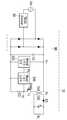
도 3은 본 발명의 실시예에 따른 교류-직류 변환기를 포함하는 회로도를 나타낸다.3 shows a circuit diagram comprising an AC-DC converter according to an embodiment of the present invention.
도 3에 도시된 바와 같이 본 발명의 실시예에 따른 교류-직류 변환기(30)는 입력단에 교류 전원(Vac) 및 트라이액 딤머(10)가 직렬로 연결되어 있고, 출력단에 로드(RL)이 연결되어 있다.As shown in FIG. 3, in the AC-
교류-직류 변환기(30)는 브리지 다이오드(BD), 입력 커패시터(C2), 블리드 스위치 회로(200), 블리드 스위치 제어부(100), 전력 스위치(T1), 저항(R3), 트랜스포머(TX), 다이오드(D1)를 포함한다.The AC-
브리지 다이오드(BD)는 4개의 다이오드로 구성되며, 교류 전원(Vac)과 트라이액 딤머(10)가 각각 연결된 2개의 입력단 및 정류된 교류 전압(V+)을 출력하는 2개의 출력단을 가진다.The bridge diode BD is composed of four diodes, and has two input terminals connected to the AC power source Vac and the
입력 커패시터(C2)는 정류된 교류 전압(V+)에 연결되어 정류된 교류 전압(V+)을 안정화시키고 전자파 잡음(Electromagnetic Interference, EMI)을 감소시킨다.The input capacitor C2 is connected to the rectified AC voltage V + to stabilize the rectified AC voltage V + and reduce electromagnetic interference (EMI).
블리드 스위치 제어부(100)는 전력 스위치(T1)의 소스 전압(V1)을 이용해서 블리드 스위치 제어 신호(Vg)를 생성한다.The
트랜스포머(TX)는 1차 코일(Co1)과 2차 코일(Co2)을 포함한다. 1차 코일(Co1)의 일단은 브리지 다이오드(BD)의 출력단 중 하나와 연결되고, 1차 코일(Co1)의 타단은 전력 스위치(T1)의 드레인 전극과 연결된다. 2차 코일(Co2)의 일단은 다이오드(D1)의 애노드에 연결되어 있다. 로드(RL)의 일단은 다이오드(D1)의 타단에 연결되고, 로드(RL)의 타단은 2차 코일(Co2)의 타단에 연결된다.The transformer TX includes a primary coil Co1 and a secondary coil Co2. One end of the primary coil Co1 is connected to one of the output terminals of the bridge diode BD, and the other end of the primary coil Co1 is connected to the drain electrode of the power switch T1. One end of the secondary coil Co2 is connected to the anode of the diode D1. One end of the rod RL is connected to the other end of the diode D1, and the other end of the rod RL is connected to the other end of the secondary coil Co2.
전력 스위치(T1)의 게이트 전극은 전력 스위치 제어 신호(Vout)가 공급되고, 전력 스위치(T1)의 소스는 저항(R3)의 일단과 연결된다.The gate electrode of the power switch T1 is supplied with the power switch control signal Vout, and the source of the power switch T1 is connected to one end of the resistor R3.
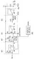
다음은 도 4와 도 5를 참고하여 본 발명의 실시예에 따른 블리드 스위치 제어부(100)와 블리드 스위치 회로(200)를 설명한다. 특히, 도 4와 도 5에서 보여주는 블리드 스위치 제어부(100)는 하나의 IC로 구현될 수 있으나, 이에 한정될 필요는 없다.Next, the
도 4는 본 발명의 한 실시예에 따른 블리드 스위치 제어부와 블리드 스위치 회로를 보여주는 회로도이다.4 is a circuit diagram illustrating a bleed switch controller and a bleed switch circuit according to an exemplary embodiment of the present invention.
도 4에 도시된 바와 같이, 블리드 스위치 제어부(100)는 디지털 제어부(120), 아날로그 제어부(130)를 포함하고, 블리드 스위치 회로(200)는 저항(R11), 고전압 스위치(Ta), 블리드 저항(RBLEED)을 포함한다.As illustrated in FIG. 4, the
디지털 제어부(120)는 블리드 스위치 온-오프 제어 신호(Vd)를 생성한다. 아날로그 제어부(130)는 전력 스위치(T1)의 소스 전압(V1) 및 블리드 스위치 온-오프 제어 신호(Vd)를 입력으로 하여, 블리드 스위치 제어 신호(Vg)를 생성한다.The
도 4의 실시예에 따르면, 고전압 스위치(Ta)는 저항(R11)의 일단에 연결된 드레인 전극, 블리드 스위치 제어 신호(Vg)에 연결된 게이트 전극 및 블리드 저항(RBLEED)의 일단에 연결된 소스 전극을 포함한다. 저항(R11)은 고전압 스위치(Ta)의 드레인 전극에 연결된 일단 및 정류된 교류 전압(V+)에 연결된 타단을 포함한다.According to the embodiment of FIG. 4, the high voltage switch Ta may include a drain electrode connected to one end of the resistor R11, a gate electrode connected to the bleed switch control signal Vg, and a source electrode connected to one end of the bleed resistor RBLEED . Include. The resistor R11 includes one end connected to the drain electrode of the high voltage switch Ta and the other end connected to the rectified AC voltage V +.
도 5는 본 발명의 다른 실시예에 따른 블리드 스위치 제어부와 블리드 스위치 회로를 보여주는 회로도이다.5 is a circuit diagram illustrating a bleed switch controller and a bleed switch circuit according to another exemplary embodiment of the present invention.
도 5에 도시된 바와 같이, 블리드 스위치 제어부(100)는 디지털 제어부(120), 아날로그 제어부(130), 저전압 NMOS 트랜지스터(Tb), 블리드 저항(RBLEED)을 포함한다. 이 경우, 고전압이 저전압 NMOS 트랜지스터(Tb)에 입력되는 것을 방지하기 위하여, 고전압 스위치(Tc), 저항(R21), 저항(R22), 제너 다이오드(D21), 및 커패시터(C21)를 포함하는 블리드 스위치 회로(200)가 저전압 NMOS 트랜지스터(Tb)에 연결된다.As illustrated in FIG. 5, the
디지털 제어부(120)는 블리드 스위치 온-오프 제어 신호(Vd)를 생성한다. 아날로그 제어부(130)는 전력 스위치(T1)의 소스 전압(V1) 및 블리드 스위치 온-오프 제어 신호(Vd)를 입력으로 하여, 블리드 스위치 제어 신호(Vg)를 생성한다.The
도 5의 실시예에 따르면, 고전압 스위치(Tc)의 소스 전극에 연결된 드레인 전극, 블리드 스위치 제어 신호(Vg)에 연결된 게이트 전극 및 블리드 저항(RBLEED)의 일단에 연결된 소스 전극을 포함한다. 고전압 스위치(Tc)는 저항(R21)의 일단에 연결된 드레인 전극, 커패시터(C21)의 일단에 연결된 게이트 전극, 저전압 NMOS 트랜지스터(Tb)의 드레인 전극에 연결된 소스 전극을 포함한다. 저항(R21)은 고전압 스위치(Tc)의 소스 전극에 연결된 일단 및 정류된 교류 전압(V+)에 연결된 타단을 포함한다. 저항(R22)은 커패시터(C21)의 일단에 연결된 일단 및 정류된 교류 전압(V+)에 연결된 타단을 포함한다. 커패시터(C21)는 고전압 스위치(Tc)의 게이트 전극에 연결된 일단 및 그라운드에 연결된 타단을 포함한다. 제너 다이오드(D21)는 커패시터의 일단에 연결된 애노드 및 그라운드에 연결된 캐소드를 포함한다.5 includes a drain electrode connected to the source electrode of the high voltage switch Tc, a gate electrode connected to the bleed switch control signal Vg, and a source electrode connected to one end of the bleed resistor RBLEED . The high voltage switch Tc includes a drain electrode connected to one end of the resistor R21, a gate electrode connected to one end of the capacitor C21, and a source electrode connected to the drain electrode of the low voltage NMOS transistor Tb. The resistor R21 includes one end connected to the source electrode of the high voltage switch Tc and the other end connected to the rectified AC voltage V +. The resistor R22 includes one end connected to one end of the capacitor C21 and the other end connected to the rectified AC voltage V +. The capacitor C21 includes one end connected to the gate electrode of the high voltage switch Tc and the other end connected to the ground. Zener diode D21 includes an anode connected to one end of a capacitor and a cathode connected to ground.
다음은 도 6을 참조하여 본 발명의 실시예에 따른 블리드 스위치 제어부(100)를 상세히 설명한다.Next, the
도 6은 본 발명의 실시예에 따른 디지털 제어부를 보여주는 회로도이다.6 is a circuit diagram illustrating a digital controller according to an embodiment of the present invention.
디지털 제어부(120)는 블리드 스위치 온-오프 제어 신호(Vd)를 생성한다. 예를 들어, 블리드 스위치 온-오프 제어 신호(Vd)는 2개의 레벨을 가질 수 있다. 블리드 스위치 온-오프 제어 신호(Vd)가 2개의 레벨 중 하나인 경우, 블리드 스위치 회로(200)는 턴온되고, 블리드 스위치 온-오프 제어 신호(Vd)가 2개의 레벨 중 다른 하나인 경우, 블리드 스위치 회로(200)는 턴오프될 수 있다. 후술하겠지만, 본 발명의 실시예에서 블리드 스위치 온-오프 신호(Vd)가 하이 레벨에 해당하는 경우, 블리드 스위치 회로(200)는 턴오프된다.The
도 6에 도시된 바와 같이, 디지털 제어부(120)는 트랜지스터(T2), 비교기(U1a), NOT 게이트(U1b), AND 게이트(U1c), 카운터(U1d), 비교기(U1e), 숏 펄스 트리거(U1f), NOT 게이트(U1g), AND 게이트(U1h), 래치(U1i), 및 NAND 게이트(U1j)를 포함한다.As shown in FIG. 6, the
비교기(U1a)는 참조 전압(CS_REF)에 연결된 비반전 단자(+), 아날로그 제어부(130)가 출력하는 샘플링 신호(Vs)에 연결된 반전 단자(-), 및 출력 단자를 포함한다. NOT 게이트(U1b)는 전력 스위치 제어 신호(Vout)에 연결된 입력 단자 및 출력 단자를 포함한다. AND 게이트(U1c)는 비교기(U1a)의 출력 단자 및 NOT 게이트(U1b)의 출력 단자에 각각 연결된 2개의 입력 단자 및 출력 단자를 포함한다. 카운터(U1d)는 AND 게이트(U1c)의 출력 단자에 연결된 입력 단자, NOT 게이트(U1h)의 출력 단자에 연결된 리셋 단자, 및 출력 단자를 포함한다. 트랜지스터(T2)는 정류된 교류 전압(V+)에 연결된 드레인 전극, 그라운드에 연결된 게이트 전극, 및 소스 전극을 포함한다. 비교기(U1e)는 트랜지스터(T2)의 소스 전극에 연결된 비반전 단자(+), 참조 전압(V+_REF)에 연결된 반전 단자(-), 및 출력 단자를 포함한다. 숏 펄스 트리거(U1f)는 비교기(U1e)의 출력 단자에 연결된 입력 단자 및 출력 단자를 포함한다. NOT 게이트(U1g)는 숏 펄스 트리거(U1f)의 출력 단자에 연결된 입력 단자 및 출력 단자를 포함한다. AND 게이트(U1h)는 카운터(U1d)의 출력 단자 및 NOT 게이트(U1g)의 출력 단자에 각각 연결된 2개의 입력 단자 및 출력 단자를 포함한다. 래치(U1i)는 AND 게이트(U1h)의 출력 단자에 연결된 셋 단자(S), 숏 펄스 트리거(U1f)의 출력 단자에 연결된 리셋 단자(R), 및 출력 단자(Q)를 포함한다. NAND 게이트(U1j)는 래치(U1i)의 출력 단자(Q)와 비교기(U1e)의 출력 단자에 각각 연결된 2개의 입력 단자 및 블리드 스위치 온-오프 제어 신호(Vd)를 출력하는 출력 단자를 포함한다. 디지털 제어부(120)의 동작에 대해서는 후술한다.The comparator U1a includes a non-inverting terminal + connected to the reference voltage CS_REF, an inverting terminal (-) connected to the sampling signal Vs output from the
도 7은 본 발명의 실시예에 따른 아날로그 제어부를 보여주는 회로도이다.7 is a circuit diagram illustrating an analog controller according to an exemplary embodiment of the present invention.
아날로그 제어부(130)는 전력 스위치(T1)의 소스 전압(V1) 및 블리드 스위치 온-오프 제어 신호(Vd)를 입력으로 하여, 블리드 스위치 제어 신호(Vg)를 생성한다.The
도 7에 도시된 바와 같이, 본 발명의 실시예에 따른 아날로그 제어부(130)는 로우 패스 필터(131a), 아날로그 버퍼(131b), 샘플링부(132), 인버터 앰프(133), 트랙킹부(134), 앰프(135) 및 트랙킹 클럭 신호 생성부(136)를 포함한다.As shown in FIG. 7, the
로우 패스 필터(131a)는 전력 스위치(T1)의 소스 전압(V1)을 로우 패스 필터링하여 필터링된 신호(Vcs)를 출력한다. 로우 패스 필터(110)는 전력 스위치(T1)의 소스 전압(V1)의 노이즈를 제거하기 위한 목적 등으로 사용될 수 있다. 본 발명의 실시예에 따른 로우 패스 필터(131a)는 저항(R4), 커패시터(C3)를 포함한다. 저항(R4)은 전력 스위치(T1)의 소스 전극에 연결된 일단 및 커패시터(C3)의 일단에 연결된 타단을 포함한다. 커패시터(C3)는 저항(R4)의 타단에 연결되어 필터링된 신호(Vcs)를 출력하는 일단 및 그라운드에 연결된 타단을 포함한다.The
아날로그 버퍼(131b)는 필터링된 신호(Vcs)가 임피던스의 변화에 의해 변하지 않도록 하는 것으로, OP 앰프(U4)를 포함한다. OP 앰프(U4)는 필터링된 신호(Vcs)에 연결된 비반전 단자(+), OP 앰프(operational amplifier)(U4)의 출력 단자에 연결된 반전 단자(-), 및 버퍼링된 신호를 출력하는 출력 단자를 포함한다.The
샘플링부(132)는 아날로그 버퍼(131)의 출력 전압을 샘플링하여 샘플링 신호(Vs)를 생성한다. 샘플링부(132)는 트랜지스터(T3), 저항(R6), 커패시터(C4)를 포함한다. 트랜지스터(T3)는 OP 앰프(U4)의 출력 단자에 연결된 드레인 전극, 전력 스위치 제어 신호(Vout)에 연결된 게이터 전극을 포함한다. 저항(R6)은 트랜지스터(T3)의 소스 전극에 연결된 일단 및 커패시터(T4)의 일단에 연결된 타단을 포함한다. 커패시터(T4)는 샘플링 신호(Vs)를 출력하는 일단 및 그라운드에 연결된 타단을 포함한다.The
인버터 앰프(133)는 샘플링 신호(Vs)의 위상을 반전하여 반전된 샘플링 신호를 출력한다. 인버터 앰프(133)는 OP 앰프(U5), 트랜지스터(T4), 저항(Ra), 및 저항(Rb)를 포함한다. OP 앰프(U5)는 샘플링 신호(Vs)가 입력되는 비반전 단자(+),트랜지스터(T4)의 소스 전극에 연결된 반전 단자(-), 및 트랜지스터(T4)의 게이트 전극에 연결된 출력 단자를 포함한다. 트랜지스터(T4)는 저항(Ra)의 일단에 연결되어 반전된 샘플링 신호를 출력하는 드레인 전극, OP 앰프(U5)의 출력 단자에 연결된 게이트 전극 및 저항(Ra)의 일단에 연결된 소스 전극을 포함한다. 저항(Ra)은 트랜지스터(T4)의 드레인 전극에 연결된 일단 및 전압(Vsource)에 연결된 타단을 포함한다. 저항(Rb)은 트랜지스터(T4)의 소스 전극에 연결된 일단 및 그라운드에 연결된 타단을 포함한다.The
트랙킹 클럭 신호 생성부(136)는 전력 스위치 제어 신호(Vout)를 이용하여 트랙킹을 위한 클럭 신호(Vt_clk)를 생성한다.The tracking
트랙킹부(134)는 트랙킹을 위한 클럭 신호(Vt_clk), 인버터 앰프(133)가 출력하는 반전된 샘플링 신호, 블리드 스위치 온-오프 제어 신호(Vd)를 입력으로 하여 트랙킹 신호(Vt)를 출력한다. 트랙킹부(134)는 트랜지스터(T5), 트랜지스터(T6), 저항(R7), 커패시터(C5)를 포함한다. 트랜지스터(T5)는 트랜지스터(T4)의 드레인 전극에 연결된 드레인 전극, 트랙킹을 위한 클럭 신호(Vt_clk)에 연결된 게이트 전극 및 저항(R7)의 일단에 연결된 소스 전극을 포함한다. 저항(R7)은 트랜지스터(T5)의 소스 전극에 연결된 일단 및 커패시터(C5)의 일단에 연결되고 트랙킹 신호(Vt)를 출력하는 타단을 포함한다. 트랜지스터(T6)는 커패시터(C5)의 일단에 연결된 드레인 전극, 블리드 스위치 온-오프 제어 신호(Vd)에 연결된 게이트 전극 및 그라운드에 연결된 소스 전극을 포함한다. 커패시터(C5)는 트랜지스터(T6)의 드레인 전극에 연결된 일단 및 그라운드에 연결된 타단을 포함한다.The
앰프(135)는 트랙킹 신호(Vt)를 블리드 스위치 회로(200)에 적합한 크기로 증폭하여 블리드 스위치 제어 신호(Vg)를 출력한다. 앰프(135)는 OP 앰프(U6), 저항(Rc), 저항(Rd)를 포함한다. OP 앰프(U6)는 트랙킹 신호(Vt)에 연결된 비반전 단자(+), 저항(Rd)의 일단 및 저항(Rc)의 일단에 연결된 반전 단자(-), 및 저항(Rd)의 타단에 연결되고 블리드 스위치 제어 신호(Vg)를 출력하는 출력 단자를 포함한다. 저항(Rc)은 OP 앰프(U6)의 반전 단자(-)에 연결된 일단 및 그라운드에 연결된 타단을 포함한다. 저항(Rd)은 OP 앰프(U6)의 반전 단자(-)에 연결된 일단 및 OP 앰프(U6)의 출력 단자에 연결된 타단을 포함한다.The
다음은 도 8을 참조하여 본 발명의 실시예에 따른 블리드 스위치 제어부(100)의 동작을 설명한다.Next, an operation of the
도 8은 본 발명의 실시예에 따른 블리드 스위치 제어부의 동작을 보여주는 파형도이다.8 is a waveform diagram illustrating an operation of a bleed switch controller according to an exemplary embodiment of the present invention.
먼저, 아날로그 제어부(130)의 동작을 설명한다.First, the operation of the
정류된 교류 전압(V+)는 트라이액 딤머(10)에 의해 도 8에 도시된 형상을 갖는다. 정류된 교류 전압(V+)의 크기가 작아질수록 일정한 전력의 변환을 위하여 전력 스위치(T1)의 온타임 펄스들 사이의 간격은 줄어든다.The rectified AC voltage V + has the shape shown in FIG. 8 by the
전력 스위치(T1)가 턴온되는 시간 동안 트랜스포머(TX)의 1차 코일(Co1)에 의해 저항(R3)에 흐르는 전류의 크기는 V+/L의 기울기로 증가하므로 전력 스위치(T1)의 소스 전압(V1)에 해당하는 필터링된 신호(Vcs)의 파형은 도 8과 같이 나타난다. 특히, 정류된 교류 전압(V+)의 크기가 작은 구간에서는 1차 코일(Co1)에 인가되는 전압의 크기가 작으므로 필터링된 신호(Vcs)의 피크 값 또한 작아진다.During the time that the power switch T1 is turned on, the magnitude of the current flowing through the resistor R3 by the primary coil Co1 of the transformer TX increases with a slope of V + / L, so that the source voltage of the power switch T1 ( The waveform of the filtered signal Vcs corresponding to V1) is shown in FIG. 8. In particular, in the section where the rectified AC voltage V + is small, the magnitude of the voltage applied to the primary coil Co1 is small, so that the peak value of the filtered signal Vcs is also reduced.
아날로그 버퍼(131b)는 필터링된 신호(Vcs)에 대해 아날로그 버퍼링을 수행하여 버퍼링된 신호를 출력한다. 샘플링부(132)의 트랜지스터(T3)는 전력 스위치 제어 신호(Vout)가 하이 레벨을 갖는 경우 턴온된다. 따라서, 전력 스위치 제어 신호(Vout)가 하이 레벨을 갖는 구간에서 샘플링 신호(Vs)는 아날로그 버퍼(131b)의 출력 신호에 트랜지스터(T3)의 드레인-소스 간 전압(Vds)을 더한 것과 같다. 한편, 전력 스위치 제어 신호(Vout)가 로우 레벨을 갖는 경우 트랜지스터(T3)는 턴오프되므로, 커패시터(C4)에 충전된 전압값이 샘플링 신호(Vs)의 크기와 같다. 따라서, 전력 스위치 제어 신호(Vout)가 로우 레벨을 갖는 구간에서 샘플링 신호(Vs)는 전력 스위치 제어 신호(Vout)의 폴링 에지 순간의 샘플링 신호(Vs)의 크기로 유지된다.The
다음, 디지털 제어부(120)의 동작을 설명한다.Next, the operation of the
비교기(U1a)는 샘플링 신호(Vs)를 참조 전압(CS_REF)와 비교하여 신호(V3)를 출력한다. 구체적으로 본 발명의 실시예에 따른 비교기(U1a)는 참조 전압(CS_REF)이 샘플링 신호(Vs)보다 큰 경우에 하이 레벨의 신호를 출력하고, 반대의 경우에 로우 레벨의 신호를 출력한다.The comparator U1a outputs the signal V3 by comparing the sampling signal Vs with the reference voltage CS_REF. In detail, the comparator U1a according to the embodiment of the present invention outputs a high level signal when the reference voltage CS_REF is greater than the sampling signal Vs and a low level signal when the reference voltage CS_REF is greater than the sampling signal Vs.
NOT 게이트(U1b)는 전력 스위치 제어 신호(Vout)를 인버팅하여 신호(V2)를 출력한다.The NOT gate U1b outputs the signal V2 by inverting the power switch control signal Vout.
AND 게이트(U1c)는 NOT 게이트(U1b)의 출력 신호(V2)와 비교기(U1a)의 출력 신호(V3)를 AND 연산하여 도 8에 도시된 바와 같은 신호(V4)를 출력한다. AND 게이트(U1c)의 출력 신호(V4)는 전력 스위치 제어 신호(Vout)가 하이 레벨인 동안 샘플링 신호(Vs)가 참조 전압(CS_REF)보다 작은 조건을 검출하여 생성된 신호이며, 카운터(U1d)와 래치(U1i)에 의해 노이즈 필터링된다.The AND gate U1c performs an AND operation on the output signal V2 of the NOT gate U1b and the output signal V3 of the comparator U1a, and outputs a signal V4 as shown in FIG. 8. The output signal V4 of the AND gate U1c is a signal generated by detecting a condition in which the sampling signal Vs is less than the reference voltage CS_REF while the power switch control signal Vout is at a high level, and the counter U1d. And noise are filtered by the latch U1i.
한편, 비교기(U1e)는 정류된 교류 신호(V+)와 참조 전압(V+_REF)를 비교하여 신호(V5)를 출력한다. 구체적으로 비교기(U1e)는 참조 전압(V+_REF)이 정류된 교류 신호(V+)보다 큰 경우에 로우 레벨의 신호를 출력하고, 반대의 경우에 하이 레벨의 신호를 출력한다. 비교기(U1e)의 출력 신호(V5)는 트라이액(TRIAC)이 턴 오프되어 있는 경우에 블리드 스위치 회로(200)를 턴 오프하기 위하여 사용된다.On the other hand, the comparator U1e compares the rectified AC signal V + with the reference voltage V + _REF and outputs a signal V5. Specifically, the comparator U1e outputs a low level signal when the reference voltage V + _REF is greater than the rectified AC signal V +, and outputs a high level signal when the reference voltage V + _REF is larger than the rectified AC signal V +. The output signal V5 of the comparator U1e is used to turn off the
트라이액(TRIAC)이 트리거되면 숏 펄스 트리거(U1f)는 비교기(U1e)의 출력 신호(V5)의 라이징 에지에서 숏 펄스를 생성하여 신호(V6)을 출력한다. NOT 게이트(U1g)는 숏 펄스 트리거(U1f)의 출력 신호(V6)를 인버팅하여 신호(V7)을 출력한다. 숏 펄스 트리거(U1f)의 출력 신호(V6)과 NOT 게이트(U1g)의 출력 신호(V7)는 트라이액(TRIAC)이 트리거될 때 래치(U1i)와 카운터(U1d)를 각각 리셋하는데 사용된다.When the triac TRIAC is triggered, the short pulse trigger U1f generates a short pulse at the rising edge of the output signal V5 of the comparator U1e and outputs a signal V6. The NOT gate U1g inverts the output signal V6 of the short pulse trigger U1f to output the signal V7. The output signal V6 of the short pulse trigger U1f and the output signal V7 of the NOT gate U1g are used to reset the latch U1i and the counter U1d, respectively, when the triac TRAC is triggered.
카운터(U1d)는 NOT 게이트(U1g)의 출력 신호(V7)의 폴링 에지에서 로우 레벨을 출력하고 AND 게이트(U1c)의 출력 신호(V4)의 라이징 에지에서 위상을 전환하여, 신호(V8)을 출력한다. AND 게이트(U1h)는 카운터(U1d)의 출력 신호(V8)와 NOT 게이트(U1g)의 출력 신호(V7)을 AND 연산하여 도 8에 도시된 바와 같은 신호(V9)를 출력한다.The counter U1d outputs a low level at the falling edge of the output signal V7 of the NOT gate U1g and shifts the phase at the rising edge of the output signal V4 of the AND gate U1c to convert the signal V8. Output The AND gate U1h performs an AND operation on the output signal V8 of the counter U1d and the output signal V7 of the NOT gate U1g, and outputs a signal V9 as shown in FIG. 8.
래치(U1i)는 AND 게이트(U1h)의 출력 신호(V9)의 라이징 에지에서 하이 레벨의 신호(V10)를 출력하고, 숏 펄스 트리거(U1f)의 출력 신호(V6)의 라이징 에지에서 로우 레벨의 신호(V10)를 출력한다.The latch U1i outputs a high level signal V10 at the rising edge of the output signal V9 of the AND gate U1h, and has a low level at the rising edge of the output signal V6 of the short pulse trigger U1f. Output the signal V10.
NAND 게이트(U1j)는 래치(U1i)의 출력 신호(V10)와 비교기(U1e)의 출력 신호(V5)를 NAND 연산하여 도 8에 도시된 바와 같은 블리드 스위치 온-오프 제어 신호(Vd)를 출력한다.The NAND gate U1j performs an NAND operation on the output signal V10 of the latch U1i and the output signal V5 of the comparator U1e to output the bleed switch on-off control signal Vd as shown in FIG. 8. do.
다시, 아날로그 제어부(130)의 동작을 설명한다.The operation of the
인버터 앰프(133)는 샘플링 신호(Vs)를 -Ra/Rb의 이득으로 반전 증폭하여 반전된 샘플링 신호를 생성한다.The
한편, 트랙킹 클럭 신호 생성부(136)는 전력 스위치 제어 신호(Vout)의 폴링 에지에서 펄스를 생성하여 트랙킹 클럭 신호(Vt_clk)를 생성한다.The tracking
이로 인하여 전력 스위치 제어 신호(Vout)의 폴링 에지에서 트랜지스터(T5)가 턴온되므로, 트랙킹 신호(Vt)는 전력 스위치 제어 신호(Vout)의 폴링 에지에서의 반전된 샘플링 신호의 크기를 갖는다. 그러나, 블리드 스위치 온-오프 신호가 하이 레벨을 갖는 경우, 트랜지스터(T6)가 턴온되므로 트랙킹 신호(Vt)는 로우 레벨을 갖는다. 즉, 블리드 스위치 온-오프 신호가 하이 레벨을 갖는 구간에서 트랙킹 신호(Vt)는 로우 레벨을 갖고, 블리드 스위치 온-오프 신호가 로우 레벨을 갖는 구간에서 정류된 교류 신호(V+)의 크기가 작을수록 트랙킹 신호(Vt)는 큰 값을 갖는다.As a result, since the transistor T5 is turned on at the falling edge of the power switch control signal Vout, the tracking signal Vt has the magnitude of the inverted sampling signal at the falling edge of the power switch control signal Vout. However, when the bleed switch on-off signal has a high level, the tracking signal Vt has a low level because the transistor T6 is turned on. That is, in the section in which the bleed switch on-off signal has a high level, the tracking signal Vt has a low level, and the magnitude of the rectified AC signal V + in the section in which the bleed switch on-off signal has a low level is small. The recording tracking signal Vt has a large value.
앰프(135)는 트랙킹 신호(Vt)를 샘플링 신호(Vs)를 Rd/Rc의 이득으로 증폭하여 블리드 스위치 제어 신호(Vg)를 생성한다.The
이상에서 설명한 본 발명의 실시예는 장치 및 방법을 통해서만 구현이 되는 것은 아니며, 본 발명의 실시예의 구성에 대응하는 기능을 실현하는 프로그램 또는 그 프로그램이 기록된 기록 매체를 통해 구현될 수도 있으며, 이러한 구현은 앞서 설명한 실시예의 기재로부터 본 발명이 속하는 기술분야의 전문가라면 쉽게 구현할 수 있는 것이다.The embodiments of the present invention described above are not only implemented by the apparatus and method but may be implemented through a program for realizing the function corresponding to the configuration of the embodiment of the present invention or a recording medium on which the program is recorded, The embodiments can be easily implemented by those skilled in the art from the description of the embodiments described above.
이상에서 본 발명의 실시예에 대하여 상세하게 설명하였지만 본 발명의 권리범위는 이에 한정되는 것은 아니고 다음의 청구범위에서 정의하고 있는 본 발명의 기본 개념을 이용한 당업자의 여러 변형 및 개량 형태 또한 본 발명의 권리범위에 속하는 것이다.While the present invention has been particularly shown and described with reference to exemplary embodiments thereof, it is to be understood that the invention is not limited to the disclosed exemplary embodiments, It belongs to the scope of right.
트라이액 딤머(10), 교류 전원(Vac), 로드(20),
가변 저항(R1), 저항(R2), 커패시터(C1), 다이액(DIAC), 트라이액(TRIAC)
교류-직류 변환기(30), 브리지 다이오드(BD), 입력 커패시터(C2),
블리드 스위치 회로(200), 블리드 스위치 제어부(100), 전력 스위치(T1),
저항(R3), 트랜스포머(TX), 다이오드(D1), 디지털 제어부(120),
아날로그 제어부(130), 저항(R11), 고전압 스위치(Ta),
블리드 저항(RBLEED), 저전압 NMOS 트랜지스터(Tb), 고전압 스위치(Tc),
저항(R21), 저항(R22), 제너 다이오드(D21), 커패시터(C21),
트랜지스터(T2), 비교기(U1a), NOT 게이트(U1b), AND 게이트(U1c),
카운터(U1d), 비교기(U1e), 숏 펄스 트리거(U1f), NOT 게이트(U1g),
AND 게이트(U1h), 래치(U1i), NAND 게이트(U1j),
로우 패스 필터(131a), 아날로그 버퍼(131b), 샘플링부(132),
인버터 앰프(133), 트랙킹부(134), 앰프(135),
트랙킹 클럭 신호 생성부(136), 저항(R4), 커패시터(C3), OP 앰프(U4),
트랜지스터(T3), 저항(R6), 커패시터(C4), OP 앰프(U5), 트랜지스터(T4),
저항(Ra), 저항(Rb), 트랜지스터(T5), 트랜지스터(T6), 저항(R7),
커패시터(C5), OP 앰프(U6), 저항(Rc), 저항(Rd)Triac Dimmer (10), AC Power (Vac), Rod (20),
Variable resistor (R1), resistor (R2), capacitor (C1), diac (DIAC), triac (TRIAC)
AC-
Bleed
Resistor (R3), transformer (TX), diode (D1), digital controller (120),
Bleed resistor (RBLEED ), low voltage NMOS transistor (Tb), high voltage switch (Tc),
Resistor R21, resistor R22, zener diode D21, capacitor C21,
Transistor T2, comparator U1a, NOT gate U1b, AND gate U1c,
Counter U1d, Comparator U1e, Short Pulse Trigger U1f, NOT Gate U1g,
AND gate U1h, latch U1i, NAND gate U1j,
Tracking
Transistor T3, resistor R6, capacitor C4, OP amplifier U5, transistor T4,
Resistor Ra, resistor Rb, transistor T5, transistor T6, resistor R7,
Capacitor (C5), OP Amp (U6), Resistor (Rc), Resistor (Rd)
Claims (19)
Translated fromKorean제1 시간 구간에서 제1 레벨을 갖고 제2 시간 구간에서 제2 레벨을 갖는 제1제어 신호를 생성하는 제1 제어부; 및
상기 제1 제어 신호를 이용하여 제2 제어 신호를 생성하여 상기 블리드 스위치에 제공하는 제2 제어부를 포함하고,
상기 제1 시간 구간에서 상기 블리드 스위치는 턴오프되고,
상기 제2 시간 구간에서 상기 블리드 스위치는 턴온되는 제어 장치.In the control device for controlling the bleed switch,
A first control unit generating a first control signal having a first level in a first time interval and having a second level in a second time interval; And
A second control unit generating a second control signal using the first control signal and providing the second control signal to the bleed switch;
The bleed switch is turned off in the first time interval,
And the bleed switch is turned on in the second time interval.
상기 제1 시간 구간에서 전력 스위치의 전류의 세기는 상기 제2 시간 구간에서 전력 스위치의 전류의 세기보다 큰 제어 장치.The method of claim 1,
The control device of the current intensity of the power switch in the first time interval is greater than the intensity of the current of the power switch in the second time interval.
상기 제2 제어 신호는 상기 제1 시간 구간에서 제3 레벨을 갖고, 상기 제2 시간 구간 내의 제3 시간 구간에서 제4 레벨을 갖고, 상기 제2 시간 구간 내의 제4 시간 구간에서 제5 레벨을 갖는 제어 장치.The method of claim 2,
The second control signal has a third level in the first time interval, has a fourth level in the third time interval in the second time interval, and has a fifth level in the fourth time interval in the second time interval. Having a control device.
상기 제3 시간 구간에서 전력 스위치의 전류의 세기는 상기 제4 시간 구간에서 전력 스위치의 전류의 세기보다 큰 제어 장치.The method of claim 3,
The strength of the current of the power switch in the third time interval is a control device larger than the strength of the current of the power switch in the fourth time interval.
상기 제4 레벨에서 상기 블리드 스위치의 전류의 세기는 상기 제5 레벨에서 상기 블리드 스위치의 전류의 세기보다 작은 제어 장치.The method of claim 4, wherein
The control device of the current level of the bleed switch at the fourth level is less than the intensity of the current of the bleed switch at the fifth level.
상기 제2 제어부는
상기 전력 스위치의 전류에 해당하는 전압을 샘플링하여 샘플링 신호를 출력하는 샘플링부;
상기 샘플링 신호를 반전하여 반전된 신호를 생성하는 인버터; 및
상기 제1 제어 신호 및 상기 반전된 신호를 이용하여 상기 제2 제어 신호를 생성하는 제3 제어부를 포함하는 제어 장치.The method of claim 2,
The second control unit
A sampling unit configured to output a sampling signal by sampling a voltage corresponding to a current of the power switch;
An inverter configured to invert the sampling signal to generate an inverted signal; And
And a third controller configured to generate the second control signal using the first control signal and the inverted signal.
상기 제3 제어부는
상기 전력 스위치의 제어 신호를 이용하여 클럭 신호를 생성하는 클럭 생성부;
상기 제1 제어 신호가 상기 제1 레벨을 갖는 경우 제3 레벨을 갖고, 상기 제1 제어 신호가 제2 레벨을 갖는 경우 상기 클럭 신호의 에지에 해당하는 상기 샘플링 신호의 레벨을 갖는 트랙킹 신호를 생성하는 트랙킹부; 및
상기 트랙킹 신호를 증폭하여 상기 제2 제어 신호를 생성하는 증폭부를 포함하는 제어 장치.The method of claim 6,
The third control unit
A clock generator configured to generate a clock signal using the control signal of the power switch;
Generating a tracking signal having a third level when the first control signal has the first level and having a level of the sampling signal corresponding to an edge of the clock signal when the first control signal has a second level; Tracking unit to; And
And an amplifier configured to amplify the tracking signal to generate the second control signal.
상기 샘플링 신호는 상기 전력 스위치의 상태가 턴오프일 때에 상기 전력 스위치의 상태가 턴오프되기 직전의 상기 전력 스위치의 전류에 해당하는 레벨을 갖는 제어 장치.The method of claim 6,
And the sampling signal has a level corresponding to a current of the power switch immediately before the state of the power switch is turned off when the state of the power switch is turned off.
상기 샘플링 신호는 상기 전력 스위치의 상태가 턴온일 때에 상기 전력 스위치의 전류에 해당하는 레벨을 갖는 제어 장치.The method of claim 8,
And the sampling signal has a level corresponding to a current of the power switch when the state of the power switch is turned on.
상기 트라이액 딤머와 연결된 AC-DC 컨버터를 포함하고,
상기 AC-DC 컨버터는
전력 스위치와,
블리드 스위치와,
제1 시간 구간에서 상기 블리드 스위치를 턴오프하고 제2 시간 구간에서 상기 블리드 스위치를 턴온하는 블리드 스위치 제어부를 포함하는 전원 장치.Triac dimmers; And
An AC-DC converter connected to the triac dimmer,
The AC-DC converter
With power switch,
Bleed switch,
And a bleed switch controller to turn off the bleed switch in a first time interval and turn on the bleed switch in a second time interval.
상기 제1 시간 구간에서 상기 전력 스위치의 전류의 세기는 상기 제2 시간 구간에서 상기 전력 스위치의 전류의 세기보다 큰 전원 장치.The method of claim 10,
The power supply of the current of the power switch in the first time interval is greater than the power of the current of the power switch in the second time interval.
상기 블리드 스위치 제어부는 상기 제2 시간 구간 내의 제3 시간 구간에서 상기 블리드 스위치의 전류의 세기를 상기 제2 시간 구간 내의 제4 시간 구간에서 상기 블리드 스위치의 전류의 세기 보다 작도록 상기 블리드 스위치를 제어하는 전원 장치.The method of claim 11,
The bleed switch controller controls the bleed switch so that the intensity of the current of the bleed switch is smaller than the intensity of the current of the bleed switch in a fourth time interval in the second time interval within the second time interval. Power unit.
상기 제3 시간 구간에서 상기 전력 스위치의 전류의 세기는 상기 제4 시간 구간에서 상기 전력 스위치의 전류의 세기보다 큰 전원 장치.The method of claim 12,
The power supply of the current of the power switch in the third time interval is greater than the power of the current of the power switch in the fourth time interval.
제1 시간 구간에서 제1 레벨을 갖고 제2 시간 구간에서 제2 레벨을 갖는 제1제어 신호를 생성하는 단계; 및
상기 제1 제어 신호를 이용하여 제2 제어 신호를 생성하여 상기 블리드 스위치에 제공하는 단계를 포함하고,
상기 제1 시간 구간에서 상기 블리드 스위치는 턴오프되고,
상기 제2 시간 구간에서 상기 블리드 스위치는 턴온되는 구동 방법.In the driving method of the power supply device, the power consumption is controlled by the triac dimmer, and including a bleed switch,
Generating a first control signal having a first level in a first time interval and having a second level in a second time interval; And
Generating a second control signal using the first control signal and providing the second control signal to the bleed switch;
The bleed switch is turned off in the first time interval,
And the bleed switch is turned on in the second time interval.
상기 제1 시간 구간에서 전력 스위치의 전류의 세기는 상기 제2 시간 구간에서 전력 스위치의 전류의 세기보다 큰 구동 방법.15. The method of claim 14,
And a strength of the current of the power switch in the first time period is greater than the strength of the current of the power switch in the second time period.
상기 제2 제어 신호는 상기 제1 시간 구간에서 제3 레벨을 갖고, 상기 제2 시간 구간 내의 제3 시간 구간에서 제4 레벨을 갖고, 상기 제2 시간 구간 내의 제4 시간 구간에서 제5 레벨을 갖는 구동 방법.16. The method of claim 15,
The second control signal has a third level in the first time interval, has a fourth level in the third time interval in the second time interval, and has a fifth level in the fourth time interval in the second time interval. Having a driving method.
상기 제3 시간 구간에서 전력 스위치의 전류의 세기는 상기 제4 시간 구간에서 전력 스위치의 전류의 세기보다 큰 구동 방법.The method of claim 16,
The strength of the current of the power switch in the third time period is greater than the strength of the current of the power switch in the fourth time interval.
상기 제4 레벨에서 상기 블리드 스위치의 전류의 세기는 상기 제5 레벨에서 상기 블리드 스위치의 전류의 세기보다 작은 구동 방법.18. The method of claim 17,
And the intensity of the current of the bleed switch at the fourth level is less than the intensity of the current of the bleed switch at the fifth level.
상기 제2 제어 신호를 생성하는 단계는,
상기 전력 스위치의 상태가 턴오프일 때에 상기 전력 스위치의 상태가 턴오프되기 직전의 상기 전력 스위치의 전류에 해당하는 레벨을 갖고, 상기 전력 스위치의 상태가 턴온일 때에 상기 전력 스위치의 전류에 해당하는 레벨을 갖는 샘플링 신호를 생성하는 단계와,
상기 샘플링 신호를 반전하여 반전된 신호를 생성하는 단계와,
상기 전력 스위치의 제어 신호를 이용하여 클럭 신호를 생성하는 단계와,
상기 제1 제어 신호가 상기 제1 레벨을 갖는 경우 제3 레벨을 갖고, 상기 제1 제어 신호가 제2 레벨을 갖는 경우 상기 클럭 신호의 에지에 해당하는 상기 샘플링 신호의 레벨을 갖는 트랙킹 신호를 생성하는 단계와,
상기 트랙킹 신호를 증폭하여 상기 제2 제어 신호를 생성하는 단계를 포함하는 구동 방법.19. The method of claim 18,
Generating the second control signal,
When the state of the power switch is turned off has a level corresponding to the current of the power switch immediately before the state of the power switch is turned off, and when the state of the power switch is turned on corresponding to the current of the power switch Generating a sampling signal having a level,
Inverting the sampling signal to generate an inverted signal;
Generating a clock signal using a control signal of the power switch;
Generating a tracking signal having a third level when the first control signal has the first level and having a level of the sampling signal corresponding to an edge of the clock signal when the first control signal has a second level; To do that,
Amplifying the tracking signal to generate the second control signal.
Priority Applications (3)
| Application Number | Priority Date | Filing Date | Title |
|---|---|---|---|
| KR1020110002378AKR20120080908A (en) | 2011-01-10 | 2011-01-10 | Apparatus for controlling bleed switch, power supply, and method for driving power supply |
| US13/238,944US8803434B2 (en) | 2011-01-10 | 2011-09-21 | Apparatus for controlling bleed switch, power supply, and method for driving power supply |
| CN2011103549394ACN102595691A (en) | 2011-01-10 | 2011-11-10 | Apparatus for controlling bleed switch, power supply, and method for driving power supply |
Applications Claiming Priority (1)
| Application Number | Priority Date | Filing Date | Title |
|---|---|---|---|
| KR1020110002378AKR20120080908A (en) | 2011-01-10 | 2011-01-10 | Apparatus for controlling bleed switch, power supply, and method for driving power supply |
Publications (1)
| Publication Number | Publication Date |
|---|---|
| KR20120080908Atrue KR20120080908A (en) | 2012-07-18 |
Family
ID=46454753
Family Applications (1)
| Application Number | Title | Priority Date | Filing Date |
|---|---|---|---|
| KR1020110002378AWithdrawnKR20120080908A (en) | 2011-01-10 | 2011-01-10 | Apparatus for controlling bleed switch, power supply, and method for driving power supply |
Country Status (3)
| Country | Link |
|---|---|
| US (1) | US8803434B2 (en) |
| KR (1) | KR20120080908A (en) |
| CN (1) | CN102595691A (en) |
Cited By (2)
| Publication number | Priority date | Publication date | Assignee | Title |
|---|---|---|---|---|
| CN103219874A (en)* | 2013-03-20 | 2013-07-24 | 北京市信息技术研究所 | Direct-current modulation power supply drain electrode modulation device of unmanned machine |
| CN116250376A (en)* | 2020-08-14 | 2023-06-09 | 赤多尼科两合股份有限公司 | Control circuit, LED driver and control method |
Families Citing this family (15)
| Publication number | Priority date | Publication date | Assignee | Title |
|---|---|---|---|---|
| US9093903B2 (en) | 2011-09-28 | 2015-07-28 | Monolithic Power Systems, Inc. | Power converter with voltage window and the method thereof |
| US20130343090A1 (en)* | 2012-06-21 | 2013-12-26 | Fairchild Korea Semiconductor Ltd. | Active bleeder, active bleeding method, and power supply device where the active bleeder is applied |
| US8742672B2 (en)* | 2012-07-26 | 2014-06-03 | Iml International | Light source dimming control circuit |
| CN102892224A (en)* | 2012-09-13 | 2013-01-23 | 南京中电熊猫照明有限公司 | Circuit for implementing more than two switch information on single phase line by utilizing phase method |
| EP2890220B1 (en)* | 2013-12-24 | 2023-10-25 | Silergy Semiconductor (Hong Kong) Limited | Bleeder circuit controller |
| CN103841725B (en)* | 2014-03-05 | 2016-01-20 | 上海晶丰明源半导体有限公司 | To release control module, controllable silicon light modulation LED drive circuit and system |
| CN104020377A (en)* | 2014-06-13 | 2014-09-03 | 成都芯源系统有限公司 | LED driving device, controller thereof and dimming mode detection method |
| US9214851B1 (en) | 2014-07-02 | 2015-12-15 | Power Integrations, Inc. | Trailing edge detector using current collapse |
| KR20160055694A (en)* | 2014-11-10 | 2016-05-18 | 페어차일드코리아반도체 주식회사 | Standby current supplier |
| FR3045270B1 (en)* | 2015-12-14 | 2019-11-22 | Delta Dore | METHOD AND DEVICE FOR MANAGING THE OPERATION OF A LIGHTING DEVICE |
| CN106912144B (en)* | 2017-04-06 | 2018-01-23 | 矽力杰半导体技术(杭州)有限公司 | LED drive circuit, circuit module and control method with controllable silicon dimmer |
| US10237932B1 (en)* | 2018-05-02 | 2019-03-19 | Iml International | Light-emitting diode lighting system with automatic bleeder current control |
| CN109673079B (en)* | 2018-12-19 | 2024-06-04 | 宁波格立光电科技有限公司 | Silicon controlled rectifier dimming active bleeder control circuit |
| CN110582144B (en)* | 2019-10-14 | 2024-07-16 | 深圳市明微电子股份有限公司 | Self-adaptive bleeder control circuit and method |
| CN111864714B (en)* | 2020-09-02 | 2025-01-24 | 厦门金龙联合汽车工业有限公司 | An electric energy discharge device and method for electric vehicle bus capacitor |
Family Cites Families (10)
| Publication number | Priority date | Publication date | Assignee | Title |
|---|---|---|---|---|
| US4234819A (en)* | 1979-06-14 | 1980-11-18 | Purex Corporation | Underwater light circuit and installation |
| US5512810A (en)* | 1994-05-27 | 1996-04-30 | Eaton Corporation | Variable speed control for a hand-held electric power tool |
| US5914591A (en)* | 1996-12-25 | 1999-06-22 | Matsushita Electric Industrial Co., Ltd. | Switching power supply |
| JP4774903B2 (en)* | 2005-10-17 | 2011-09-21 | サンケン電気株式会社 | Switching power supply |
| WO2007088577A1 (en)* | 2006-01-31 | 2007-08-09 | Mitsumi Electric Co., Ltd. | Switching power supply apparatus and semiconductor integrated circuit for controlling power supply |
| US7880445B2 (en)* | 2006-02-16 | 2011-02-01 | Summit Microelectronics, Inc. | System and method of charging a battery using a switching regulator |
| EP2286637B1 (en)* | 2008-06-04 | 2016-11-16 | Nxp B.V. | Dc-dc converter |
| US8169165B2 (en)* | 2009-01-14 | 2012-05-01 | Mag Instrument, Inc. | Multi-mode portable lighting device |
| US8299730B2 (en)* | 2010-02-09 | 2012-10-30 | Power Integrations, Inc. | Integrated on-time extension for non-dissipative bleeding in a power supply |
| US8111017B2 (en)* | 2010-07-12 | 2012-02-07 | O2Micro, Inc | Circuits and methods for controlling dimming of a light source |
- 2011
- 2011-01-10KRKR1020110002378Apatent/KR20120080908A/ennot_activeWithdrawn
- 2011-09-21USUS13/238,944patent/US8803434B2/enactiveActive
- 2011-11-10CNCN2011103549394Apatent/CN102595691A/enactivePending
Cited By (2)
| Publication number | Priority date | Publication date | Assignee | Title |
|---|---|---|---|---|
| CN103219874A (en)* | 2013-03-20 | 2013-07-24 | 北京市信息技术研究所 | Direct-current modulation power supply drain electrode modulation device of unmanned machine |
| CN116250376A (en)* | 2020-08-14 | 2023-06-09 | 赤多尼科两合股份有限公司 | Control circuit, LED driver and control method |
Also Published As
| Publication number | Publication date |
|---|---|
| US20120176055A1 (en) | 2012-07-12 |
| US8803434B2 (en) | 2014-08-12 |
| CN102595691A (en) | 2012-07-18 |
Similar Documents
| Publication | Publication Date | Title |
|---|---|---|
| KR20120080908A (en) | Apparatus for controlling bleed switch, power supply, and method for driving power supply | |
| US10448469B2 (en) | Systems and methods for intelligent dimming control using TRIAC dimmers | |
| CN102412727B (en) | Switching power supply, control circuit thereof and dimming method | |
| US10952300B2 (en) | LED driver and controller thereof, and LED lighting device | |
| US9660519B2 (en) | Switching power supply circuit and power factor correction circuit | |
| US20200389958A1 (en) | Systems and methods for current regulation in light-emitting-diode lighting systems | |
| US9485816B2 (en) | Method and apparatus for dimmable LED driver | |
| US10849201B2 (en) | Driving circuit and driving method for driving light-emitting diode load | |
| US20120299572A1 (en) | Input current regulator, driving method thereof, and disable circuit thereof | |
| KR20100023770A (en) | Circuit arrangement for operating at least one semiconductor light source | |
| RU2604640C2 (en) | High efficiency light-emitting diode circuit | |
| KR20160116275A (en) | Currrent compensation circuit and light apparatus comprising the same | |
| US9590615B1 (en) | Integrated circuit and switching power-supply device performing output control through switching operation | |
| JP7256384B2 (en) | Power supply device, semiconductor integrated circuit and ripple suppression method | |
| US9220138B1 (en) | Soft bleeder to remove step dimming | |
| KR102207626B1 (en) | Currrent compensation circuit and light apparatus comprising the same | |
| KR101188236B1 (en) | Apparatus for lighting control of lighting device | |
| KR20170010957A (en) | Trigger circuit, light apparatus comprising the same and trigger method | |
| KR20150078614A (en) | Power driver for LED(light emitting diode) illumination and control method thereof | |
| JP5810306B2 (en) | LED lighting device and lighting apparatus using the same | |
| KR20160147177A (en) | Switching contorl circuit, light apparatus comprising the same and switching control method |
Legal Events
| Date | Code | Title | Description |
|---|---|---|---|
| PA0109 | Patent application | Patent event code:PA01091R01D Comment text:Patent Application Patent event date:20110110 | |
| PG1501 | Laying open of application | ||
| PC1203 | Withdrawal of no request for examination | ||
| WITN | Application deemed withdrawn, e.g. because no request for examination was filed or no examination fee was paid |