KR20120076816A - Optical sheet, ptical apparatus and method for manufacturing the optical sheet - Google Patents
Optical sheet, ptical apparatus and method for manufacturing the optical sheetDownload PDFInfo
- Publication number
- KR20120076816A KR20120076816AKR1020100138537AKR20100138537AKR20120076816AKR 20120076816 AKR20120076816 AKR 20120076816AKR 1020100138537 AKR1020100138537 AKR 1020100138537AKR 20100138537 AKR20100138537 AKR 20100138537AKR 20120076816 AKR20120076816 AKR 20120076816A
- Authority
- KR
- South Korea
- Prior art keywords
- pattern
- prism
- resin
- pitch
- prism pattern
- Prior art date
- Legal status (The legal status is an assumption and is not a legal conclusion. Google has not performed a legal analysis and makes no representation as to the accuracy of the status listed.)
- Ceased
Links
Images


Classifications
- G—PHYSICS
- G02—OPTICS
- G02B—OPTICAL ELEMENTS, SYSTEMS OR APPARATUS
- G02B5/00—Optical elements other than lenses
- G02B5/02—Diffusing elements; Afocal elements
- G02B5/0268—Diffusing elements; Afocal elements characterized by the fabrication or manufacturing method
- B—PERFORMING OPERATIONS; TRANSPORTING
- B29—WORKING OF PLASTICS; WORKING OF SUBSTANCES IN A PLASTIC STATE IN GENERAL
- B29D—PRODUCING PARTICULAR ARTICLES FROM PLASTICS OR FROM SUBSTANCES IN A PLASTIC STATE
- B29D11/00—Producing optical elements, e.g. lenses or prisms
- B29D11/0074—Production of other optical elements not provided for in B29D11/00009- B29D11/0073
- B29D11/00788—Producing optical films
- G—PHYSICS
- G02—OPTICS
- G02B—OPTICAL ELEMENTS, SYSTEMS OR APPARATUS
- G02B5/00—Optical elements other than lenses
- G02B5/02—Diffusing elements; Afocal elements
- G02B5/0205—Diffusing elements; Afocal elements characterised by the diffusing properties
- G02B5/021—Diffusing elements; Afocal elements characterised by the diffusing properties the diffusion taking place at the element's surface, e.g. by means of surface roughening or microprismatic structures
- G02B5/0231—Diffusing elements; Afocal elements characterised by the diffusing properties the diffusion taking place at the element's surface, e.g. by means of surface roughening or microprismatic structures the surface having microprismatic or micropyramidal shape
- G—PHYSICS
- G02—OPTICS
- G02B—OPTICAL ELEMENTS, SYSTEMS OR APPARATUS
- G02B5/00—Optical elements other than lenses
- G02B5/04—Prisms
- G02B5/045—Prism arrays
- G—PHYSICS
- G02—OPTICS
- G02B—OPTICAL ELEMENTS, SYSTEMS OR APPARATUS
- G02B6/00—Light guides; Structural details of arrangements comprising light guides and other optical elements, e.g. couplings
- G02B6/0001—Light guides; Structural details of arrangements comprising light guides and other optical elements, e.g. couplings specially adapted for lighting devices or systems
- G02B6/0011—Light guides; Structural details of arrangements comprising light guides and other optical elements, e.g. couplings specially adapted for lighting devices or systems the light guides being planar or of plate-like form
- G02B6/0033—Means for improving the coupling-out of light from the light guide
- G02B6/005—Means for improving the coupling-out of light from the light guide provided by one optical element, or plurality thereof, placed on the light output side of the light guide
- G02B6/0053—Prismatic sheet or layer; Brightness enhancement element, sheet or layer
- G—PHYSICS
- G02—OPTICS
- G02F—OPTICAL DEVICES OR ARRANGEMENTS FOR THE CONTROL OF LIGHT BY MODIFICATION OF THE OPTICAL PROPERTIES OF THE MEDIA OF THE ELEMENTS INVOLVED THEREIN; NON-LINEAR OPTICS; FREQUENCY-CHANGING OF LIGHT; OPTICAL LOGIC ELEMENTS; OPTICAL ANALOGUE/DIGITAL CONVERTERS
- G02F1/00—Devices or arrangements for the control of the intensity, colour, phase, polarisation or direction of light arriving from an independent light source, e.g. switching, gating or modulating; Non-linear optics
- G02F1/01—Devices or arrangements for the control of the intensity, colour, phase, polarisation or direction of light arriving from an independent light source, e.g. switching, gating or modulating; Non-linear optics for the control of the intensity, phase, polarisation or colour
- G02F1/13—Devices or arrangements for the control of the intensity, colour, phase, polarisation or direction of light arriving from an independent light source, e.g. switching, gating or modulating; Non-linear optics for the control of the intensity, phase, polarisation or colour based on liquid crystals, e.g. single liquid crystal display cells
- G02F1/133—Constructional arrangements; Operation of liquid crystal cells; Circuit arrangements
- G02F1/1333—Constructional arrangements; Manufacturing methods
- G02F1/1335—Structural association of cells with optical devices, e.g. polarisers or reflectors
- G02F1/1336—Illuminating devices
- G02F1/133602—Direct backlight
- G02F1/133606—Direct backlight including a specially adapted diffusing, scattering or light controlling members
- G02F1/133607—Direct backlight including a specially adapted diffusing, scattering or light controlling members the light controlling member including light directing or refracting elements, e.g. prisms or lenses
Landscapes
- Physics & Mathematics (AREA)
- General Physics & Mathematics (AREA)
- Optics & Photonics (AREA)
- Engineering & Computer Science (AREA)
- Manufacturing & Machinery (AREA)
- Health & Medical Sciences (AREA)
- Ophthalmology & Optometry (AREA)
- Mechanical Engineering (AREA)
- Optical Elements Other Than Lenses (AREA)
Abstract
Description
Translated fromKorean본 발명은 광학 시트, 광학 장치 및 광학 시트의 제조방법에 관한 것으로, 보다 상세하게는 휘도 향상 및 열에 의한 시트의 변형을 방지할 수 있는 광학 시트, 광학 장치 및 광학 시트의 제조방법에 관한 것이다.
The present invention relates to an optical sheet, an optical device, and a manufacturing method of the optical sheet, and more particularly, to an optical sheet, an optical device, and a manufacturing method of the optical sheet which can prevent deformation of the sheet due to brightness enhancement and heat.
액정 디스플레이(liquid crystal display, LCD)는 현재 가장 널리 사용되고 있는 평판 디스플레이(flat panel display) 중 하나이다. 일반적으로 액정 디스플레이는 TFT(Thin Film Transistor) 어레이 기판과 칼라필터 기판 사이에 액정층이 봉입된 구조를 취한다. 상기 어레이 기판과 칼라필터 기판에 존재하는 전극에 전기장을 인가하면 그 사이에 봉입된 액정층의 액정 분자의 배열이 변하게 되고, 이를 이용해 영상을 표시하게 된다.Liquid crystal displays (LCDs) are one of the most widely used flat panel displays. In general, a liquid crystal display has a structure in which a liquid crystal layer is enclosed between a thin film transistor (TFT) array substrate and a color filter substrate. When an electric field is applied to the electrodes on the array substrate and the color filter substrate, the arrangement of the liquid crystal molecules of the liquid crystal layer enclosed therebetween changes, thereby displaying an image.
액정 디스플레이는 자체 발광하지 않으므로 백라이트 유닛이 필요하며, 상기 백라이트 유닛은 통상 발광다이오드(LED) 또는 형광 램프(CCFL) 등의 광원, 도광판, 휘도향상시트(프리즘시트), 확산시트, 보호시트 등으로 구성되어 있다.The liquid crystal display does not emit light by itself, and thus requires a backlight unit. The backlight unit is a light source such as a light emitting diode (LED) or a fluorescent lamp (CCFL), a light guide plate, a brightness enhancement sheet (prism sheet), a diffusion sheet, a protective sheet, or the like. Consists of.
그런데, 상기 광원에 의해 발생하는 열에 의해 상기 시트들의 변형이 발생하는 문제점이 있으며, 최근의 대형화, 고휘도화 추세에 따라 휘도가 더욱 개선된 광학 시트 및 백라이트 유닛이 필요하다. 아울러, 상기 광학 시트에 형성된 패턴 내지 액정패널의 주기적인 픽셀 구조에 기인한 모아레 현상이 발생하지 않는 광학 시트 및 백라이트 유닛, 액정 디스플레이 등의 광학 장치가 필요하다.
However, there is a problem in that deformation of the sheets occurs due to heat generated by the light source, and an optical sheet and a backlight unit having a further improved luminance in accordance with the recent trend toward larger size and higher luminance are needed. In addition, there is a need for an optical sheet, such as a back light unit, a liquid crystal display, and an optical sheet, in which a moire phenomenon does not occur due to a periodic pixel structure of a liquid crystal panel or a pattern formed on the optical sheet.
본 발명의 하나의 목적은 휘도 특성 및 내열성이 우수하면서도 모아레가 발생하지 않는 광학 시트, 광학 장치 및 광학 시트의 제조방법을 제공하는 것이다.One object of the present invention is to provide an optical sheet, an optical device, and a method for manufacturing the optical sheet, which are excellent in luminance characteristics and heat resistance but do not generate moiré.
본 발명의 다른 목적은 제조공정이 간단하고 제조비용과 시간을 절감할 수 있는 광학 시트 제조방법 및 이에 의해 제조된 광학 시트, 이를 구비한 광학 장치를 제공하는 것이다.
Another object of the present invention is to provide an optical sheet manufacturing method which can simplify the manufacturing process and reduce manufacturing cost and time, and an optical sheet manufactured thereby, and an optical device having the same.
본 발명의 하나의 관점은 광학 시트에 관한 것이다. 상기 광학 시트는 상면 및 이에 대향하는 하면을 갖는 베이스 시트, 상기 베이스 시트의 하면에 존재하는 제1프리즘 패턴 및 상기 베이스 시트의 상면에 존재하는 상부 패턴을 포함하되, 상기 상부 패턴은 상기 제1프리즘 패턴과 그 피치가 다른 제2프리즘 패턴, 렌티큘러 패턴, 상기 제1프리즘 패턴의 피치와 다른 직경을 갖는 마이크로렌즈 패턴 또는 피치가 존재하지 않는 불규칙한 엠보 패턴인 것을 특징으로 한다.One aspect of the invention relates to an optical sheet. The optical sheet includes a base sheet having an upper surface and a lower surface opposite thereto, a first prism pattern present on a lower surface of the base sheet, and an upper pattern present on an upper surface of the base sheet, wherein the upper pattern is the first prism. And a second prism pattern, a lenticular pattern, a microlens pattern having a diameter different from that of the first prism pattern, or an irregular embossed pattern without a pitch.
구체예에서, 상기 베이스 시트, 상기 제1프리즘 패턴 및 상기 상부 패턴은 동일한 물질로 이루어질 수 있다.In some embodiments, the base sheet, the first prism pattern, and the upper pattern may be made of the same material.
구체예에서, 상기 제1프리즘 패턴은 동일한 프리즘이 서로 인접해 배열되어 있는 규칙적인 패턴일 수 있다.In embodiments, the first prism pattern may be a regular pattern in which the same prism is arranged adjacent to each other.
구체예에서, 상기 제1프리즘 패턴을 형성하는 프리즘은 적어도 2개의 프리즘면을 갖는 다각프리즘일 수 있다.In embodiments, the prism forming the first prism pattern may be a polygonal prism having at least two prism faces.
구체예에서, 상기 제1프리즘 패턴을 형성하는 프리즘은 삼각프리즘이며, 상기 삼각프리즘의 꼭지각이 70도 내지 110도일 수 있다.In embodiments, the prism forming the first prism pattern is a triangular prism, the vertex of the triangular prism may be 70 degrees to 110 degrees.
구체예에서, 상기 제1프리즘 패턴의 피치, 제2프리즘 패턴의 피치, 렌티큘러 패턴의 피치 또는 마이크로렌즈 패턴을 형성하는 마이크로렌즈의 직경이 5㎛ 내지 150㎛일 수 있다.In embodiments, the pitch of the first prism pattern, the pitch of the second prism pattern, the pitch of the lenticular pattern or the diameter of the microlens forming the microlens pattern may be 5㎛ to 150㎛.
구체예에서, 상기 제1프리즘 패턴의 피치와 상기 제2프리즘 패턴의 피치의 차이의 절대값 또는 상기 제1프리즘 패턴의 피치와 상기 렌티큘러 패턴의 피치의 차이의 절대값이 0.1㎛ 내지 50㎛일 수 있다.In embodiments, the absolute value of the difference between the pitch of the first prism pattern and the pitch of the second prism pattern or the absolute value of the difference between the pitch of the first prism pattern and the pitch of the lenticular pattern is 0.1㎛ to 50㎛ Can be.
구체예에서, 상기 제1프리즘 패턴의 피치와 상기 마이크로렌즈 패턴을 형성하는 마이크로렌즈의 직경(D)의 차이의 절대값이 0.1㎛ 내지 70㎛일 수 있다.In embodiments, the absolute value of the difference between the pitch of the first prism pattern and the diameter (D) of the microlens forming the microlens pattern may be 0.1 μm to 70 μm.
구체예에서, 상기 베이스 시트, 제1프리즘 패턴 또는 상부 패턴은 폴리아세탈 수지, 아크릴계 수지, 폴리카보네이트 수지, 스티렌계 수지, 폴리에스테르 수지, 비닐계 수지, 폴리페닐렌에테르 수지, 폴리올레핀 수지, 시클로올레핀계 수지, 아크릴로니트릴-부타디엔-스티렌 공중합체 수지, 폴리아릴레이트 수지, 폴리아릴설폰 수지, 폴리에테르설폰 수지, 폴리페닐렌 설피드 수지, 폴리에틸렌 나프탈레이트 수지, 폴리에틸렌 수지 또는 불소계 수지 중 어느 하나 이상을 포함할 수 있다.
In embodiments, the base sheet, the first prism pattern or the upper pattern is a polyacetal resin, acrylic resin, polycarbonate resin, styrene resin, polyester resin, vinyl resin, polyphenylene ether resin, polyolefin resin, cycloolefin Any one or more of a series resin, acrylonitrile-butadiene-styrene copolymer resin, polyarylate resin, polyarylsulfone resin, polyethersulfone resin, polyphenylene sulfide resin, polyethylene naphthalate resin, polyethylene resin or fluorine-based resin It may include.
본 발명의 다른 관점은 광학 장치에 관한 것이다. 상기 광학 장치는 전술한 광학 시트를 포함한다.
Another aspect of the invention relates to an optical device. The optical device includes the optical sheet described above.
본 발명의 또 다른 관점은 광학 시트 제조방법에 관한 것이다. 상기 광학 시트 제조방법은 제1용융수지공급부에서 제1용융수지를 공급하며 용융 상태의 웹을 형성하는 단계, 상기 웹을 제1패턴형성롤러와 제2패턴형성롤러 사이로 통과시켜 상기 하면에 제1프리즘 패턴, 상기 하면에 대향하는 상면에 상부 패턴을 형성하는 단계 및 상기 제1프리즘 패턴과 상부 패턴이 형성된 웹을 냉각시키는 단계를 포함하되, 상기 상부 패턴은 상기 제1프리즘 패턴과 그 피치가 다른 제2프리즘 패턴, 렌티큘러 패턴, 상기 제1프리즘 패턴의 피치와 다른 직경을 갖는 마이크로렌즈 패턴 또는 피치가 존재하지 않는 불규칙한 엠보 패턴인 것을 특징으로 한다.Another aspect of the invention relates to a method for producing an optical sheet. In the optical sheet manufacturing method, a first molten resin is supplied from a first molten resin supply unit to form a web in a molten state, and the web is passed between a first pattern forming roller and a second pattern forming roller to form a first on the lower surface. Forming an upper pattern on an upper surface opposite to the lower surface of the prism pattern, and cooling the web on which the first prism pattern and the upper pattern are formed, wherein the upper pattern is different in pitch from the first prism pattern. A second prism pattern, a lenticular pattern, a microlens pattern having a diameter different from the pitch of the first prism pattern, or an irregular embossed pattern without a pitch may be present.
구체예에서, 상기 제1용융수지공급부에서 제1용융수지를 공급하며 용융 상태의 웹을 형성하는 단계 이후, 상기 웹의 하면에 제2용융수지를, 상기 하면에 대향하는 상면에 제3용융수지를 도포하는 단계를 더 포함할 수 있다.In an embodiment, after the forming of the molten web by supplying the first molten resin from the first molten resin supply unit, the second molten resin on the lower surface of the web, the third molten resin on the upper surface opposite to the lower surface It may further comprise the step of applying.
구체예에서, 상기 제1용융수지공급부에서 제1용융수지를 공급하며 용융 상태의 웹을 형성하는 단계와 상기 웹의 하면에 제2용융수지를, 상기 하면에 대향하는 상면에 제3용융수지를 도포하는 단계 사이에, 상기 용융 상태의 웹을 냉각시키는 단계를 더 포함할 수 있다.
In an embodiment, the first molten resin supply unit supplies the first molten resin to form a molten web, a second molten resin on a lower surface of the web, and a third molten resin on an upper surface opposite to the lower surface. Between the step of applying, it may further comprise the step of cooling the web of the molten state.
본 발명의 광학 시트 및 이를 포함하는 광학 장치는 휘도 특성 및 내열성이 우수하면서도 모아레가 발생하지 않으며, 제1프리즘 패턴과 제2프리즘 패턴의 정렬이 필요없는 제조 공정상의 잇점이 있다.The optical sheet of the present invention and the optical device including the same have advantages in manufacturing process that are excellent in brightness characteristics and heat resistance, do not generate moiré, and do not require alignment of the first prism pattern and the second prism pattern.
또한, 간단한 제조공정으로 양면에 패턴이 형성된 광학 시트를 제공함으로써 광학 시트 및 이를 포함하는 광학 장치의 제조비용과 제조시간을 절감하고 생산단가를 크게 낮출 수 있다.
In addition, by providing an optical sheet having a pattern formed on both sides by a simple manufacturing process, it is possible to reduce the manufacturing cost and manufacturing time of the optical sheet and the optical device including the same, and to significantly reduce the production cost.
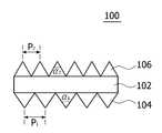
도 1은 본 발명의 한 구체예에 따른 광학 시트의 사시도이며, 도 2는 도 1의 A-A' 단면도이다.
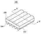
도 3은 본 발명의 다른 구체예에 따른 광학 시트의 사시도이며, 도 4는 도 3의 B-B' 단면도이다.
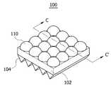
도 5는 본 발명의 또 다른 구체예에 따른 광학 시트의 사시도이며, 도 6은 도 5의 C-C' 단면도이다.
도 7은 본 발명의 또 다른 구체예에 따른 광학 시트의 사시도이다.
도 8은 본 발명의 제1프리즘 패턴의 다양한 실시예를 나타낸 것이다.
도 9는 본 발명의 한 구체예에 따른 광학 시트 제조방법을 나타낸 개념도이다.
도 10은 본 발명의 다른 구체예에 따른 광학 시트 제조방법을 나타낸 개념도이다.1 is a perspective view of an optical sheet according to an embodiment of the present invention, and FIG. 2 is a cross-sectional view taken along line AA ′ of FIG. 1.
3 is a perspective view of an optical sheet according to another embodiment of the present invention, and FIG. 4 is a cross-sectional view taken along line BB ′ of FIG. 3.
5 is a perspective view of an optical sheet according to another embodiment of the present invention, and FIG. 6 is a cross-sectional view taken along line CC ′ of FIG. 5.
7 is a perspective view of an optical sheet according to another embodiment of the present invention.
8 illustrates various embodiments of the first prism pattern of the present invention.
9 is a conceptual diagram illustrating a method of manufacturing an optical sheet according to an embodiment of the present invention.
10 is a conceptual diagram showing a method for manufacturing an optical sheet according to another embodiment of the present invention.
도 1은 본 발명의 한 구체예에 따른 광학 시트의 사시도이며, 도 2는 도 1의 A-A' 단면도이다. 도 1 및 도 2에 도시된 것과 같이, 본 발명의 한 구체예에 따른 광학 시트(100)는 베이스 시트(102), 제1프리즘 패턴 및 상부 패턴을 포함한다. 상기 제1프리즘 패턴은 그 피치가 존재하는 규칙적인 프리즘 패턴일 수 있으며 상부 패턴의 피치와는 다르게 구성될 수 있다. 상기 프리즘의 꼭지각은 1개 이상일 수 있는데, 도 1 및 도 2에는 제1프리즘 패턴의 일례로 꼭지각이 1개인(2개의 프리즘면을 갖는) 삼각프리즘 패턴(104)을 나타내었고, 상부 패턴의 일례로서 제2프리즘 패턴(106)을 나타내었다.1 is a perspective view of an optical sheet according to an embodiment of the present invention, and FIG. 2 is a cross-sectional view taken along line AA ′ of FIG. 1. As shown in FIGS. 1 and 2, the
베이스 시트(102), 삼각프리즘 패턴(104) 및 제2프리즘 패턴(106)은 서로 동일한 물질로 이루어질 수도 있고 서로 다른 물질로 이루어질 수도 있으며, 일부만 동일한 물질로 이루어질 수도 있다. 예를 들어, 상기 베이스 시트(102), 삼각프리즘 패턴(104) 및 제2프리즘 패턴(106)은 가시광선 영역에서 투명한 재료로서 열가소성 수지 또는 그 조성물로 이루어질 수 있다. 구체적으로, 폴리아세탈 수지, 아크릴계 수지, 폴리카보네이트 수지, 스티렌계 수지, 폴리에스테르 수지, 비닐계 수지, 폴리페닐렌에테르 수지, 폴리올레핀 수지, 시클로올레핀계 수지, 아크릴로니트릴-부타디엔-스티렌 공중합체 수지, 폴리아릴레이트 수지, 폴리아릴설폰 수지, 폴리에테르설폰 수지, 폴리페닐렌 설피드 수지, 폴리에틸렌 나프탈레이트 수지, 폴리에틸렌 수지 또는 불소계 수지 중 어느 하나 이상을 포함할 수 있다.The
베이스 시트(102)의 하면(일면)에는 삼각프리즘 패턴(104)이 존재하며, 삼각프리즘 패턴(104)은 동일한 프리즘이 서로 인접하여 배열되는 프리즘 패턴일 수 있다. 상기 베이스 시트(102)의 하면과 대향하는 상면(타면)에는 제2프리즘 패턴(106)이 존재하되, 상기 삼각프리즘 패턴(104)의 피치(P1)와 제2프리즘 패턴의 피치(P2)는 서로 다르게 구성될 수 있다. 즉, 제1프리즘 패턴의 피치(P1)는 제2프리즘 패턴의 피치(P2)보다 크거나 작게 형성될 수 있다.A
또한, 삼각프리즘 패턴(104)과 제2프리즘 패턴(106)을 구성하는 프리즘의 길이 방향은 서로 동일한 것이 바람직하다. 즉, 삼각프리즘 패턴(104)과 제2프리즘 패턴(106)을 구성하는 프리즘의 산(또는 골)이 서로 나란하게 배열되는 것이 바람직하다. 다만, 본 발명에서 나란하게 배열된다는 의미는 반드시 상기 프리즘의 산(또는 골)이 일직선으로 평행해야 하는 것은 아니며, 상기 프리즘의 산(또는 골)이 곡선을 이루면서 동일 방향으로 향하는 경우도 포함되는 등 실질적으로 나란하게 배열되는 경우를 포함한다.In addition, it is preferable that the longitudinal directions of the prisms constituting the
구체예에서, 삼각프리즘 패턴(104)의 피치(P1)와 제2프리즘 패턴(106)의 피치(P2)는1㎛ 내지 200㎛, 바람직하게는 5㎛ 내지 150㎛일 수 있으며,삼각프리즘 패턴(104)의 피치(P1)와 제2프리즘 패턴(106)의 피치(P2)의 차이의 절대값(│P1-P2│)은0.1㎛ 내지 50㎛일 수 있다.또한, 삼각프리즘 패턴(104)과 제2프리즘 패턴(106)을 형성하는 프리즘의 꼭지각(α1,α2)은 60도 내지 120도, 바람직하게는 70도 내지 110도일 수 있다.In embodiments, the pitch (P2) of the pitch (P1) and a
전술한 예는 제2프리즘 패턴(106)을 형성하는 프리즘이 삼각프리즘인 경우이나 제2프리즘 패턴(106)을 형성하는 프리즘은 상기 삼각프리즘 외에 꼭지각인 2개 이상, 즉 프리즘면이 3개 이상인 다각프리즘일 수도 있다.In the above-described example, the prism forming the
상기와 같이, 베이스 시트(102)의 상면과 하면에 존재하는 프리즘 패턴을 통해 휘도 향상 및 내열성 향상을 꾀할 수 있고, 상기 두 패턴의 피치를 서로 다르게 그리고 규칙적인 정렬 없이 구성함으로써 패턴 피치가 동일하거나 정렬을 해야 하는 경우에 비해 제조공정의 간략화도 꾀할 수 있고, 아울러 규칙적인 프리즘 패턴에 의해 발생하는 모아레 현상을 방지할 수 있다.
As described above, the brightness and heat resistance may be improved through the prism patterns existing on the upper and lower surfaces of the
도 3은 본 발명의 다른 구체예에 따른 광학 시트의 사시도이며, 도 4는 도 3의 B-B' 단면도이다. 도시된 것과 같이, 본 발명의 다른 구체예에 따른 광학 시트(100)는 베이스 시트(102), 제1프리즘 패턴 및 상부 패턴을 포함한다. 상기 제1프리즘 패턴은 그 피치가 존재하는 규칙적인 프리즘 패턴일 수 있으며, 상기 프리즘의 꼭지각은 1개 이상일 수 있다. 도 3 및 도 4에는 제1프리즘 패턴의 일례로 꼭지각이 1개인 삼각프리즘 패턴(104)을 나타내었고, 상부 패턴의 일례로서 렌티큘러 패턴(108)을 나타내었다.3 is a perspective view of an optical sheet according to another embodiment of the present invention, and FIG. 4 is a cross-sectional view taken along line BB ′ of FIG. 3. As shown, the
베이스 시트(102), 삼각프리즘 패턴(104) 및 렌티큘러 패턴(108)은 가시광선 영역에서 투명한 재료로서 열가소성 수지 또는 그 조성물로 이루어질 수 있다. 예를 들어 폴리아세탈 수지, 아크릴계 수지, 폴리카보네이트 수지, 스티렌계 수지, 폴리에스테르 수지, 비닐계 수지, 폴리페닐렌에테르 수지, 폴리올레핀 수지, 시클로올레핀계 수지, 아크릴로니트릴-부타디엔-스티렌 공중합체 수지, 폴리아릴레이트 수지, 폴리아릴설폰 수지, 폴리에테르설폰 수지, 폴리페닐렌 설피드 수지, 폴리에틸렌 나프탈레이트 수지, 폴리에틸렌 수지 또는 불소계 수지 중 어느 하나 이상을 포함할 수 있다.The
베이스 시트(102)의 하면에는 삼각프리즘 패턴(104)이 존재하며, 상기 베이스 시트의 하면(일면)과 대향하는 상면(타면)에는 렌티큘러 패턴(108)이 존재하되, 상기 삼각프리즘 패턴(104)의 피치(P1)와 렌티큘러 패턴(108)의 피치(P3)는 서로 다르게 구성될 수 있다. 즉, 삼각프리즘 패턴(104)의 피치(P1)는 렌티큘러 패턴(108)의 피치(P3)보다 크거나 작게 형성된다. 또한 상기 렌티큘러 패턴(108)을 형성하는 렌티큘러는 동일한 렌티큘러가 인접하여 배열되는 형태일 수 있다.A
또한, 삼각프리즘 패턴(104)을 형성하는 프리즘과 렌티큘러 패턴(108)을 형성하는 렌티큘러의 방향은 서로 동일한 것이 바람직하다. 즉, 삼각프리즘 패턴(104)의 형성하는 프리즘의 산(또는 골)과 렌티큘러 패턴(108)을 형성하는 렌티큘러의 골(또는 마루)이 서로 나란하게 배열되는 것이 바람직하다. 다만, 본 발명에서 나란하게 배열된다는 의미는 프리즘의 산(또는 골)과 렌트큘러의 골(또는 마루)이 일직선으로 평행해야 하는 것은 아니며, 상기 프리즘의 산(또는 골)과 렌트큘러의 골(또는 마루)이 곡선을 이루면서 동일 방향으로 향하는 경우도 포함되는 등 실질적으로 나란하게 배열되는 경우를 포함하는 의미이다.In addition, it is preferable that the prism forming the
구체예에서, 렌티큘러 패턴(108)의 피치(P3)는 1㎛ 내지 200㎛, 바람직하게는 5㎛ 내지 150㎛일 수 있으며, 삼각프리즘 패턴(104)의 피치(P1)와 렌티큘러 패턴(108)의 피치(P3)의 차이의 절대값(│P1-P3│)은 0.1㎛ 내지 50㎛일 수 있다.
In an embodiment, the pitch P3 of the
도 5는 본 발명의 또 다른 구체예에 따른 광학 시트의 사시도이며, 도 6은 도 5의 C-C' 단면도이다. 도시된 것과 같이, 본 발명의 다른 구체예에 따른 광학 시트(100)는 베이스 시트(102), 제1프리즘 패턴 및 상부 패턴을 포함한다. 상기 제1프리즘 패턴은 그 피치가 존재하는 규칙적인 프리즘 패턴일 수 있으며, 상기 프리즘의 꼭지각은 1개 이상일 수 있다. 도 5 및 도 6에는 제1프리즘 패턴의 일례로 꼭지각이 1개인 삼각프리즘 패턴(104)을 나타내었고, 상부 패턴의 일례로서 마이크로렌즈 패턴(110)을 나타내었다.5 is a perspective view of an optical sheet according to another embodiment of the present invention, and FIG. 6 is a cross-sectional view taken along line C-C 'of FIG. 5. As shown, the
베이스 시트(102), 삼각프리즘 패턴(104) 및 마이크로렌즈 패턴(110)은 가시광선 영역에서 투명한 재료로서 열가소성 수지 또는 그 조성물로 이루어질 수 있다. 상기 재료의 구체적 예는 전술한 바와 같다.The
베이스 시트(102)의 하면에는 삼각프리즘 패턴(104)이 존재하며, 상기 베이스 시트의 하면(일면)과 이에 대향하는 상면(타면)에는 마이크로렌즈 패턴(110)이 존재하되, 상기 삼각프리즘 패턴(104)의 피치(P1)와 마이크로렌즈 패턴(110)의 렌즈의 직경(D)은 서로 다르게 구성될 수 있다. 즉, 삼각프리즘 패턴(104)의 피치(P1)는 마이크로렌즈 패턴(110)의 렌즈의 직경(D)보다 크거나 작게 형성될 수 있다. 구체예에서, 삼각프리즘 패턴(104)의 피치(P1)와 마이크로렌즈 패턴(110)의 마이크로렌즈의 직경(D)은 각각 1㎛ 내지 200㎛, 바람직하게는 5㎛ 내지 150㎛일 수 있으며, 삼각프리즘 패턴의 피치(P1)와 마이크로렌즈의 직경(D)의 차이의 절대값(│P1-D│)은 0.01㎛ 내지 100㎛, 바람직하게는 0.1㎛ 내지 70㎛일 수 있다.
A
도 7은 본 발명의 또 다른 구체예에 따른 광학 시트의 사시도이다. 도시된 것과 같이, 본 발명의 또 다른 구체예에 따른 광학 시트(100)는 베이스 시트(102), 제1프리즘 패턴 및 상부 패턴을 포함한다. 상기 제1프리즘 패턴은 그 피치가 존재하는 규칙적인 프리즘 패턴일 수 있으며, 상기 프리즘의 꼭지각은 1개 이상일 수 있다. 도 7에는 제1프리즘 패턴의 일례로 꼭지각이 1개인 삼각프리즘 패턴(104)을 나타내었고, 상부 패턴의 일례로서 엠보 패턴(112)을 나타내었다.7 is a perspective view of an optical sheet according to another embodiment of the present invention. As shown, the
엠보 패턴(112)은 그 직경, 높이 등이 불규칙한 요철부가 배열되어 있는 형태이며, 기타 베이스 시트(102), 삼각프리즘 패턴(104) 및 엠보 패턴(112)의 재질, 삼각프리즘 패턴(104)의 형태 등은 전술한 바와 동일하므로 그 자세한 설명을 생략하도록 한다.
The
도 8은 본 발명의 제1프리즘 패턴의 다양한 실시예를 나타낸 것이다. 도시된 것과 같이, 본 발명의 제1프리즘 패턴을 형성하는 프리즘의 꼭지각은 1개 이상, 바람직하게는 1개 내지 3개일 수 있다. 제1프리즘 패턴은 피치 P1을 갖는 규칙적인 패턴일 수 있으며, 도 8에 도시하지 않았으나 제1프리즘 패턴의 상부로 베이스 시트, 상부 패턴이 존재하며, 상부 패턴은 제1프리즘 패턴과 그 피치가 다른 제2프리즘 패턴, 렌티큘러 패턴, 상기 제1프리즘 패턴의 피치와 다른 직경을 갖는 마이크로렌즈 패턴 또는 피치가 존재하지 않는 불규칙한 엠보 패턴 등일 수 있으며 그 구체적 내용은 전술하였으므로 자세한 설명을 생략하도록 한다.8 illustrates various embodiments of the first prism pattern of the present invention. As shown, the vertex angle of the prism forming the first prism pattern of the present invention may be one or more, preferably one to three. The first prism pattern may be a regular pattern having a pitch P1 , and although not shown in FIG. 8, a base sheet and an upper pattern exist as an upper portion of the first prism pattern, and the upper pattern may have a first prism pattern and a pitch thereof. Another second prism pattern, a lenticular pattern, a microlens pattern having a diameter different from the pitch of the first prism pattern, or an irregular embossed pattern without a pitch may be used, and detailed description thereof will be omitted.
구체예에서, 상기 제1프리즘 패턴을 형성하는 프리즘은 그 꼭지각이 1개인 삼각프리즘일 수 있다(도 8(A)). 상기 삼각프리즘은 전술한 삼각프리즘 패턴(104)을 형성하는 프리즘일 수 있다. 상기 삼각프리즘은 두 개의 프리즘면(F1, F2)를 가질 수 있으며 상기 프리즘면의 단면은 직선을 이룰 수 있다. 이러한 삼각프리즘에 대해서는 전술하였으므로 그 자세한 설명을 생략하도록 한다.In an embodiment, the prism forming the first prism pattern may be a triangular prism having one vertex (FIG. 8A). The triangular prism may be a prism forming the
다른 구체예에서, 상기 제1프리즘 패턴을 형성하는 프리즘은 그 꼭지각이 1개, 즉 두 개의 프리즘면(F3, F4)이 존재하는 삼각프리즘이나 적어도 하나의 프리즘면은 곡선을 이룰 수 있다(도 8(B)). 그 단면이 곡선을 이루는 프리즘면(F4)은 하나의 곡률반경을 가질 수도 있고, 2개 이상의 곡률반경을 가질 수도 있으며, 곡률반경이 연속적으로 변하는 형태일 수도 있으며, 포물선 형태일 수도 있다. 이 경우 빛(광원)은 도면의 좌측에서 입사되어 상기 곡선 프리즘면(F4)에서 반사 또는 전반사되어 상측으로 출광될 수 있다.In another embodiment, the prism forming the first prism pattern may have one vertex angle, that is, a triangular prism having two prism faces F3 and F4 or at least one prism face may be curved. (FIG. 8 (B)). The prism surface F4 whose cross section is curved may have one radius of curvature, two or more radius of curvature, or may have a shape in which the radius of curvature is continuously changed or may be a parabolic shape. In this case, light (a light source) may be incident on the left side of the drawing and may be reflected or totally reflected on the curved prism surface F4 to be emitted upward.
또 다른 구체예에서, 상기 제1프리즘 패턴을 형성하는 프리즘은 2개의 꼭지각, 즉 3개의 프리즘면(F5, F6, F7)을 갖는 사각프리즘일 수 있다(도 8(C)).In another embodiment, the prism forming the first prism pattern may be a rectangular prism having two vertices, that is, three prism faces F5 , F6 , and F7 (FIG. 8C).
또 다른 구체예에서, 상기 제1프리즘 패턴을 형성하는 프리즘은 3개의 꼭지각, 즉 4개의 프리즘면(F8, F9, F10, F11)을 갖는 오각프리즘일 수도 있다(도 8(D)). 이때, 각 프리즘면(F8, F9, F10, F11)이 그 상부에 존재하는 베이스 시트의 평활면과 이루는 각(θ1, θ2, ….θn-1)은 아래 조건을 만족할 수 있다.In another embodiment, the prism forming the first prism pattern may be an pentagonal prism having three vertices, that is, four prism faces F8 , F9 , F10 , and F11 (FIG. 8D). )). At this time, the angles θ1 , θ2 ,... Θn-1 that each prism face F8 , F9 , F10 , F11 form with the smooth surface of the base sheet existing thereon are Can be satisfied.
θi ≠ θj.θi ≠ θj .
여기서, i ≠ j이고, 1≤i(또는 j)≤n-1이며, n은 5 이상의 자연수이다.
Here, i? J, 1? I (or j)? N-1, and n is a natural number of 5 or more.
또 다른 구체예에서, 도 8에 도시되지 않았으나, 제1프리즘 패턴을 형성하는 프리즘은 5개 이상의 프리즘면을 갖는 다각프리즘일 수 있다.
In another embodiment, although not shown in FIG. 8, the prism forming the first prism pattern may be a polygonal prism having five or more prism faces.
본 발명의 다른 관점은 광학 장치에 관한 것이다. 상기 광학 장치는 전술한 광학 시트를 포함하는 백라이트 유닛일 수 있다. 상기 백라이트 유닛으로 에지(edge)형 또는 직하형 백라이트 유닛이 가능하나, 에지형 백라이트 유닛이 보다 바람직하다. 상기 백라이트 유닛은 발광다이오드(LED), CCFL(Cold Cathode Fluorescent Lamp) 등의 광원, 도광판, 확산 시트, 보호 시트 등을 더 포함할 수 있으며, 본 발명의 광학 시트를 사용함으로써 휘도향상을 위해 종래에 2장 이상 사용하던 프리즘 시트를 1장으로 줄일 수 있는 이점이 존재한다.Another aspect of the invention relates to an optical device. The optical device may be a backlight unit including the optical sheet described above. The backlight unit may be an edge type or a direct type backlight unit, but an edge type backlight unit is more preferable. The backlight unit may further include a light source such as a light emitting diode (LED), a cold cathode fluorescent lamp (CCFL), a light guide plate, a diffusion sheet, a protective sheet, and the like. There is an advantage that the prism sheet used more than two sheets can be reduced to one sheet.
본 발명의 광학 장치는 상기 백라이트 유닛의 일명에 액정패널(도시하지 않음)이 존재하는 액정 디스플레이일 수 있다. 상기 액정패널은 상부기판과 하부기판 사이의 액정층을 포함하며, 상부기판과 하부기판 각각에는 상부 편광판과 하부 편광판이 위치할 수 있다. 상기 액정층은 TN(Twisted Nematic), STN(Super Twisted Nematic) 액정을 포함할 수도 있으며, IPS(In-Plane Switching), Super-IPS, FFS(Fringe Field Switching) 등의 수평배향 모드 액정을 포함할 수도 있고, 수직배향(VA: Vertical Alignment) 모드 액정을 포함할 수도 있다. 상기 액정패널은 패시브 매트릭스일 수도 액티브 매트릭스일 수도 있으나, TFT(Thin Film Transistor) 액티브 매트릭스 액정패널이 바람직하다. 상기 액정 디스플레이 장치는 휴대폰, 모니터, TV, 태블릿 PC, 노트북 등 전자장치의 화상표시용으로 사용될 수 있다.The optical device of the present invention may be a liquid crystal display in which a liquid crystal panel (not shown) exists in one name of the backlight unit. The liquid crystal panel may include a liquid crystal layer between an upper substrate and a lower substrate, and an upper polarizer and a lower polarizer may be positioned on each of the upper and lower substrates. The liquid crystal layer may include twisted nematic (TN) and super twisted nematic (STN) liquid crystals, and may include horizontal alignment mode liquid crystals such as IPS (In-Plane Switching), Super-IPS, and FFS (Fringe Field Switching). It may also include a vertical alignment (VA) mode liquid crystal. The liquid crystal panel may be a passive matrix or an active matrix, but a TFT (Thin Film Transistor) active matrix liquid crystal panel is preferable. The liquid crystal display device may be used for image display of an electronic device such as a mobile phone, a monitor, a TV, a tablet PC, a notebook computer, and the like.
또한, 전술한 백라이트 유닛의 일면에 액정패널 대신 사진 등을 부착하면 전자 액자가 될 수 있으며, 광고용 그림을 배치하면 광고판이 될 수도 있다.
In addition, by attaching a photo or the like instead of the liquid crystal panel to one surface of the above-described backlight unit may be an electronic picture frame, it may be an advertisement board if the advertising picture is placed.
본 발명의 다른 관점은 광학 시트 제조방법에 관한 것이다. 도 9는 본 발명의 한 구체예에 따른 광학 시트 제조방법을 나타낸 개념도이다. 도시된 것과 같이, 본 발명의 한 구체예에 따른 광학 시트 제조방법은 수지 용융체를 제1제1용융수지공급부(202)에서 공급하여 용융 상태의 웹(web)을 형성하는 단계, 상기 용융 상태의 웹을 제1패턴형성롤러(204)와 제2패턴형성롤러(206) 사이로 통과시켜 상기 웹의 하면(일면)에 제1프리즘 패턴과 상기 하면에 대향하는 상면(타면)에 상부 패턴을 형성하는 단계 및 상기 제1프리즘 패턴과 상부 패턴이 형성된 웹을 냉각하는 단계를 포함할 수 있다. 상기 상면과 하면은 편의상 붙여진 명칭이며 반드시 상, 하를 지칭하는 의미는 아니다.Another aspect of the invention relates to a method for producing an optical sheet. 9 is a conceptual diagram illustrating a method of manufacturing an optical sheet according to an embodiment of the present invention. As shown, the optical sheet manufacturing method according to an embodiment of the present invention is a step of supplying a resin melt from the first first melt
본 발명의 한 구체예에 따른 광학 시트 제조방법은 전술한 베이스 시트, 제1프리즘 패턴 및 상부 패턴을 동일한 물질로 압출하여 제조할 수 있다.Optical sheet manufacturing method according to an embodiment of the present invention can be produced by extruding the above-described base sheet, the first prism pattern and the upper pattern with the same material.
구체적으로, 먼저 베이스 시트(102)와 제1프리즘 패턴 및 상부 패턴을 구성하는 수지의 용융체를 제1용융수지공급부(202)에서 공급하여 용융 상태의 웹(100a)을 형성한다. 상기 제1용융수지공급부(202)에서 용융 상태의 수지(제1용융수지)를 공급하여 압출하는 온도는 200℃ 내지 300℃일 수 있다. 상기 제1용융수지는 열가소성 수지이고 가시광선에 투광성을 보이는 재질이면 제한이 없으며 구체적 예는 전술하였으므로 그 자세한 설명을 생략하도록 한다.Specifically, first, the melt of the resin constituting the
다음, 상기 용융 상태의 웹(100a)을 제1패턴형성롤러(204)와 제2패턴형성롤러(206) 사이로 통과시켜 하면(일면)에 제1프리즘 패턴이 그리고 상면(타면)에는 상부 패턴이 형성된 웹(100b)을 얻는다. 이때, 제1패턴형성롤러(204)와 제2패턴형성롤러(206)의 온도는 120℃ 내지 150℃일 수 있다. 상기 온도범위에서 패턴 전사율이 우수할 수 있으며 패턴형성롤러에서 수지가 쉽게 떨어질 수 있다.Next, the
다음, 제1프리즘 패턴과 상부 패턴이 형성된 웹(100b)을 냉각장치(214)에 의해 냉각시킨 후 원하는 크기로 재단하여 광학 시트를 제조할 수 있다. 이와 같이 제조된 광학 시트는 전술한 구조 및 특징을 갖는 것으로서 그 자세한 설명은 생략하도록 한다.
Next, the optical sheet may be manufactured by cooling the
도 9는 본 발명의 다른 구체예에 따른 광학 시트 제조방법을 나타낸 개념도이다. 본 발명의 다른 구체예에 따른 광학 시트 제조방법을 살펴보면, 먼저 제1용융수지공급부(202)에서 베이스 시트 형성용 용융수지(제1용융수지)를 공급하여 용융 상태의 웹(102a)을 형성(압출)할 수 있다.9 is a conceptual diagram illustrating a method of manufacturing an optical sheet according to another embodiment of the present invention. Looking at the optical sheet manufacturing method according to another embodiment of the present invention, first, the molten resin (first molten resin) for forming the base sheet from the first molten
다음, 상기 용융 상태의 웹(102a)을 제1냉각장치(208)에 의해 냉각시켜 경화시킬 수 있다. 상기 제1냉각장치(208) 및 제1냉각장치(208)에 의한 냉각 공정은 생략될 수 있다.Next, the
다음, 제2용융수지공급부(210)에 의해 상기 웹(100a)의 하면(일면)에 제1프리즘 패턴 형성용 제2용융수지(104a)를 공급하며, 제3용융수지공급부(212)를 통해 상기 하면에 대향하는 상면(타면)에 상부 패턴 형성용 제3용융수지(120a)를 공급하여 도포할 수 있다.Next, the second molten
다음, 상기 제2용융수지(104a) 및 제3용융수지(120a)가 도포된 웹(102a)을 제1패턴형성롤러(204)와 제2패턴형성롤러(206) 사이로 통과시켜 상기 하면에 제1프리즘 패턴(104b), 상기 상면에 상부 패턴(120b)을 형성할 수 있다.Next, the
다음, 상기 패턴이 형성된 웹을 제2냉각장치(214)에 의해 냉각시켜 경화한 후 소정 크기로 재단하여 광학 시트를 제조할 수 있다.
Next, the web on which the pattern is formed may be cooled and cured by the
<<실시예Example 및 And비교예Comparative example>>
실시예1 내지 실시예3, 비교예1 내지 비교예5에서 사용된 광학 시트의 하면과 상면의 패턴 형태 및 코팅 여부를 표 1에 나타내었고, 표 1에 사용된 패턴들의 구체적 데이터를 표 2에 나타내었다.
Table 1 shows the pattern form of the lower surface and the upper surface of the optical sheet used in Examples 1 to 3 and Comparative Examples 1 to 5 and whether or not the coating was performed, and specific data of the patterns used in Table 1 are shown in Table 2. Indicated.
(Solid)Refractive index
(Solid)
- 오각프리즘Pitch: 23 μm
-Pentaprism
- 피치: 50㎛-Triangular prism with 90 degree vertex
Pitch: 50 μm
- 렌즈 직경: 70㎛Microlens Pattern
Lens diameter: 70㎛
- 오각프리즘Pitch: 50 μm
-Pentaprism
Chamber를 통과시킴(약 2分 체류)110 ℃ Floating Type Drying
Pass through chamber (stay 2 minutes)
아래 표 3에는 실시예1 내지 실시예3, 비교예1 내지 비교예5의 광학 시트의 광학특성 및 내열성 평가 결과를 나타낸 것이며, 그 특성 평가는 아래와 같이 수행하였다.
Table 3 below shows the optical properties and the heat resistance evaluation results of the optical sheets of Examples 1 to 3 and Comparative Examples 1 to 5, and the characteristics were evaluated as follows.
[휘도 측정][Luminance measurement]
LED 광원을 사용하는 32" LCD用 에지(edge)형 백라이트 유닛에 샘플을 조립한 후 TOPCON社의 SR3 분광방사계를 사용하여 휘도를 측정하였다.
After assembling the sample into a 32 "LCD backlight unit using an LED light source, luminance was measured using an SR3 spectroradiometer of TOPCON.
[내열성 평가][Heat resistance evaluation]
백라이트 유닛 및 LCD 모듈까지 조립한 상태에서, 60℃×75%RH×250hr 조건 下에서 환경처리 후, 상온/상습 조건 하에서 2hr 방치한 다음, Edge-LED 광원을 사용하는 32" LCD 모듈을 점등한 상태에서 시트 변형(욺)을 평가하였다.
After assembling up to backlight unit and LCD module, after environmental treatment under 60 ℃ × 75% RH × 250hr condition, let stand for 2hr under normal temperature / humidity condition, and then turn on 32 ”LCD module using Edge-LED light source. Sheet deformation was evaluated in the state.
(强시인)With
(强 poet)
(中시인)With
(Middle poet)
(弱시인)With
(弱 poet)
(Haze 7%)Matte coating
(Haze 7%)
(弱시인)With
(弱 poet)
표 3에 나타난 바와 같이, 상면에 제2프리즘 패턴만 존재하는 비교예1에 비해 하면에 제1프리즘 패턴이 존재하고 상면에 제2프리즘 패턴, 렌티큘러 패턴 또는 마이크로렌즈 패턴이 존재하는 실시예1 내지 실시예3의 휘도가 더 높게 나타났으며, 시트 변형(욺) 현상도 나타나지 않아 내열성 특성이 우수한 것으로 나타났다. 그리고, 상면에 제2프리즘 패턴이 존재하고 하드코팅, 매트 코팅이 된 경우는 실시예1 내지 실시예3에 비해 휘도가 낮고 내열성이 좋지 않은 것으로 나타났다. 또한, 상면과 하면에 서로 피치가 동일한 제3프리즘 패턴과 제2프리즘 패턴이 존재하는 비교예5의 경우는 휘도는 실시예1과 유사하지만, 상면과 하면이 서로 간섭무늬(모아레)를 발생시키는 문제가 발생하였다.
As shown in Table 3, the first prism pattern is present on the lower surface and the second prism pattern, the lenticular pattern or the microlens pattern is present on the lower surface compared to Comparative Example 1 in which only the second prism pattern is present on the upper surface. In Example 3, the luminance was higher and the sheet was not deformed, and thus, the heat resistance was excellent. In addition, when the second prism pattern is present on the top surface, and the hard coating and the matte coating are applied, the luminance is lower and the heat resistance is not good compared to Examples 1 to 3. In addition, in Comparative Example 5 in which the third prism pattern and the second prism pattern having the same pitch are present on the upper and lower surfaces, the luminance is similar to that of Example 1, but the upper and lower surfaces generate interference patterns (moire). A problem occurred.
100 : 광학 시트 102 : 베이스 시트
104 : 삼각프리즘 패턴106 : 제2프리즘 패턴
108 : 렌티큘러 패턴110 : 마이크로렌즈 패턴
112 : 엠보 패턴202 : 제1용융수지공급부
204 : 제1패턴형성롤러206 : 제2패턴형성롤러
208 : 제1냉각장치210 : 제2용융수지공급부
212 : 제3용융수지공급부214 : 제2냉각장치100: optical sheet 102: base sheet
104: triangular prism pattern 106: second prism pattern
108: lenticular pattern 110: microlens pattern
112: embossed pattern 202: first molten resin supply unit
204: first pattern forming roller 206: second pattern forming roller
208: first cooling device 210: second molten resin supply unit
212: third molten resin supply unit 214: second cooling device
Claims (13)
Translated fromKorean상기 베이스 시트의 하면에 존재하는 제1프리즘 패턴; 및
상기 베이스 시트의 상면에 존재하는 상부 패턴을 포함하되,
상기 상부 패턴은 상기 제1프리즘 패턴과 그 피치가 다른 제2프리즘 패턴, 렌티큘러 패턴, 상기 제1프리즘 패턴의 피치와 다른 직경을 갖는 마이크로렌즈 패턴 또는 피치가 존재하지 않는 불규칙한 엠보 패턴인 광학 시트.
A base sheet having an upper surface and a lower surface opposite thereto;
A first prism pattern on the bottom surface of the base sheet; And
Including an upper pattern present on the upper surface of the base sheet,
The upper pattern may include a second prism pattern, a lenticular pattern, a microlens pattern having a different diameter from the pitch of the first prism pattern, or an irregular embossed pattern without a pitch.
The optical sheet of claim 1, wherein the base sheet, the first prism pattern, and the upper pattern are made of the same material.
The optical sheet of claim 1, wherein the first prism pattern is a regular pattern in which the same prisms are arranged adjacent to each other.
The optical sheet of claim 1, wherein the prism forming the first prism pattern is a polygonal prism having at least two prism faces.
The optical sheet of claim 1, wherein the prism forming the first prism pattern is a triangular prism, and a vertex angle of the triangular prism is 70 degrees to 110 degrees.
The optical sheet of claim 1, wherein the pitch of the first prism pattern, the pitch of the second prism pattern, the pitch of the lenticular pattern, or the diameter of the microlens forming the microlens pattern is 5 μm to 150 μm.
The absolute value of the difference between the pitch of the first prism pattern and the pitch of the second prism pattern, or the absolute value of the difference between the pitch of the first prism pattern and the pitch of the lenticular pattern. 50 micrometers optical sheet.
The optical sheet according to claim 1, wherein an absolute value of a difference between the pitch of the first prism pattern and the diameter (D) of the microlenses forming the microlens pattern is 0.1 µm to 70 µm.
The method of claim 1, wherein the base sheet, the first prism pattern or the upper pattern is a polyacetal resin, acrylic resin, polycarbonate resin, styrene resin, polyester resin, vinyl resin, polyphenylene ether resin, polyolefin resin, Cycloolefin resin, acrylonitrile-butadiene-styrene copolymer resin, polyarylate resin, polyarylsulfone resin, polyethersulfone resin, polyphenylene sulfide resin, polyethylene naphthalate resin, polyethylene resin or fluorine resin An optical sheet comprising one or more.
An optical device comprising the optical sheet of claim 1.
상기 웹을 제1패턴형성롤러와 제2패턴형성롤러 사이로 통과시켜 상기 하면에 제1프리즘 패턴, 상기 하면에 대향하는 상면에 상부 패턴을 형성하는 단계; 및
상기 제1프리즘 패턴과 상부 패턴이 형성된 웹을 냉각시키는 단계를 포함하되,
상기 상부 패턴은 상기 제1프리즘 패턴과 그 피치가 다른 제2프리즘 패턴, 렌티큘러 패턴, 상기 제1프리즘 패턴의 피치와 다른 직경을 갖는 마이크로렌즈 패턴 또는 피치가 존재하지 않는 불규칙한 엠보 패턴인 광학 시트 제조방법.
Supplying the first molten resin from the first molten resin supply unit to form a web in a molten state;
Passing the web between the first pattern forming roller and the second pattern forming roller to form a first prism pattern on the lower surface and an upper pattern on an upper surface opposite to the lower surface; And
Cooling the web on which the first prism pattern and the upper pattern are formed;
The upper pattern may include a second prism pattern different from the first prism pattern, a lenticular pattern, a microlens pattern having a diameter different from that of the first prism pattern, or an irregular emboss pattern without a pitch. Way.
The method of claim 11, wherein after the forming of the molten web by supplying the first molten resin from the first molten resin supply unit, the second molten resin on the lower surface of the web, the third surface on the upper surface opposite to the lower surface Optical sheet manufacturing method further comprising the step of applying a molten resin.
The method of claim 11, wherein the first molten resin supply unit supplies the first molten resin to form a web in a molten state, and a second molten resin on a lower surface of the web and a third molten resin on an upper surface opposite to the lower surface. Between the step of applying a resin, further comprising the step of cooling the web of the molten state.
Priority Applications (1)
| Application Number | Priority Date | Filing Date | Title |
|---|---|---|---|
| KR1020100138537AKR20120076816A (en) | 2010-12-30 | 2010-12-30 | Optical sheet, ptical apparatus and method for manufacturing the optical sheet |
Applications Claiming Priority (1)
| Application Number | Priority Date | Filing Date | Title |
|---|---|---|---|
| KR1020100138537AKR20120076816A (en) | 2010-12-30 | 2010-12-30 | Optical sheet, ptical apparatus and method for manufacturing the optical sheet |
Related Child Applications (1)
| Application Number | Title | Priority Date | Filing Date |
|---|---|---|---|
| KR1020140163813ADivisionKR20140145105A (en) | 2014-11-21 | 2014-11-21 | Optical sheet and optical apparatus using the same |
Publications (1)
| Publication Number | Publication Date |
|---|---|
| KR20120076816Atrue KR20120076816A (en) | 2012-07-10 |
Family
ID=46710383
Family Applications (1)
| Application Number | Title | Priority Date | Filing Date |
|---|---|---|---|
| KR1020100138537ACeasedKR20120076816A (en) | 2010-12-30 | 2010-12-30 | Optical sheet, ptical apparatus and method for manufacturing the optical sheet |
Country Status (1)
| Country | Link |
|---|---|
| KR (1) | KR20120076816A (en) |
Cited By (5)
| Publication number | Priority date | Publication date | Assignee | Title |
|---|---|---|---|---|
| CN103760626A (en)* | 2013-12-26 | 2014-04-30 | 明基材料有限公司 | Dimming thin film |
| KR101491467B1 (en)* | 2013-07-26 | 2015-02-11 | 희성전자 주식회사 | Backlight Unit with Improved Viewing Angle |
| KR20150034839A (en)* | 2013-09-25 | 2015-04-06 | 엘지디스플레이 주식회사 | Optical sheet and liquid crystal display device having the same |
| CN106526727A (en)* | 2016-12-23 | 2017-03-22 | 合肥乐凯科技产业有限公司 | High-brightness high-haze composite optical plate |
| KR20180001239A (en)* | 2016-06-27 | 2018-01-04 | 주식회사 케이에이피에스 | Optical sheet and method of manufacturing the same |
- 2010
- 2010-12-30KRKR1020100138537Apatent/KR20120076816A/ennot_activeCeased
Cited By (7)
| Publication number | Priority date | Publication date | Assignee | Title |
|---|---|---|---|---|
| KR101491467B1 (en)* | 2013-07-26 | 2015-02-11 | 희성전자 주식회사 | Backlight Unit with Improved Viewing Angle |
| KR20150034839A (en)* | 2013-09-25 | 2015-04-06 | 엘지디스플레이 주식회사 | Optical sheet and liquid crystal display device having the same |
| CN103760626A (en)* | 2013-12-26 | 2014-04-30 | 明基材料有限公司 | Dimming thin film |
| CN103760626B (en)* | 2013-12-26 | 2016-03-02 | 明基材料有限公司 | dimming film |
| KR20180001239A (en)* | 2016-06-27 | 2018-01-04 | 주식회사 케이에이피에스 | Optical sheet and method of manufacturing the same |
| KR101868522B1 (en)* | 2016-06-27 | 2018-07-19 | 주식회사 케이에이피에스 | Optical sheet and method of manufacturing the same |
| CN106526727A (en)* | 2016-12-23 | 2017-03-22 | 合肥乐凯科技产业有限公司 | High-brightness high-haze composite optical plate |
Similar Documents
| Publication | Publication Date | Title |
|---|---|---|
| KR102199264B1 (en) | Optical sheet, backlight unit, liquid crystal display and information equipment | |
| US8279370B2 (en) | Optical laminate film, backlight unit including the same, and liquid crystal display including the same | |
| JP7506640B2 (en) | Optical sheet laminate, backlight unit, liquid crystal display device, information device, and method for manufacturing backlight unit | |
| KR20090123418A (en) | Optical sheet, backlight unit and liquid crystal display including the same | |
| US20240295678A9 (en) | Light diffusion sheet, backlight unit, liquid crystal display device, information apparatus, and method for manufacturing light diffusion sheet | |
| JP2024056804A (en) | Light diffusion sheet | |
| JP2024123030A (en) | Optical sheet laminate, backlight unit, liquid crystal display device, information device, and method for manufacturing backlight unit | |
| KR20120076816A (en) | Optical sheet, ptical apparatus and method for manufacturing the optical sheet | |
| KR20120075059A (en) | Optical sheet and optical apparatus including the same | |
| JP7509721B2 (en) | Optical sheet laminate, backlight unit, liquid crystal display device, information device, and method for manufacturing backlight unit | |
| KR20140145105A (en) | Optical sheet and optical apparatus using the same | |
| WO2022196162A1 (en) | Light diffusion sheet, backlight unit, liquid crystal display device, and information equipment | |
| KR20130076617A (en) | Optical sheet and back light unit comprising the same | |
| KR101374362B1 (en) | Optical film, backlight unit and display apparatus using the same | |
| JP7732916B2 (en) | Backlight unit, liquid crystal display device and information device | |
| JP7429248B2 (en) | Optical sheet laminate, backlight unit, liquid crystal display device, information equipment, and method for manufacturing backlight unit | |
| TWI882803B (en) | Light diffusion sheet, backlight unit, liquid crystal display device, information device and method for manufacturing backlight unit | |
| TWI894381B (en) | Light diffusing sheet, backlight unit, liquid crystal display device, information device, and method for manufacturing light diffusing sheet | |
| WO2024154698A1 (en) | Optical sheet laminate, backlight unit, liquid-crystal display device, and information appliance | |
| JP2024101556A (en) | Optical sheet laminate, backlight unit, liquid crystal display device and information device | |
| JP2025004222A (en) | Light diffusion sheet laminate, backlight unit, liquid crystal display device and information device | |
| WO2023228684A1 (en) | Light-diffusing sheet, backlight unit, liquid crystal display device, and information apparatus | |
| JP2023174543A (en) | Light diffusion sheet, backlight unit, liquid crystal display device, and information apparatus | |
| TW202532945A (en) | Light diffusion sheet, backlight unit, liquid crystal display device, information device, and method for manufacturing backlight unit | |
| CN118265931A (en) | Composite light diffusion sheet, backlight unit, liquid crystal display device and information equipment |
Legal Events
| Date | Code | Title | Description |
|---|---|---|---|
| PA0109 | Patent application | Patent event code:PA01091R01D Comment text:Patent Application Patent event date:20101230 | |
| A201 | Request for examination | ||
| PA0201 | Request for examination | Patent event code:PA02012R01D Patent event date:20120228 Comment text:Request for Examination of Application Patent event code:PA02011R01I Patent event date:20101230 Comment text:Patent Application | |
| PG1501 | Laying open of application | ||
| E902 | Notification of reason for refusal | ||
| PE0902 | Notice of grounds for rejection | Comment text:Notification of reason for refusal Patent event date:20130502 Patent event code:PE09021S01D | |
| E90F | Notification of reason for final refusal | ||
| PE0902 | Notice of grounds for rejection | Comment text:Final Notice of Reason for Refusal Patent event date:20131216 Patent event code:PE09021S02D | |
| E601 | Decision to refuse application | ||
| PE0601 | Decision on rejection of patent | Patent event date:20140923 Comment text:Decision to Refuse Application Patent event code:PE06012S01D Patent event date:20131216 Comment text:Final Notice of Reason for Refusal Patent event code:PE06011S02I Patent event date:20130502 Comment text:Notification of reason for refusal Patent event code:PE06011S01I | |
| A107 | Divisional application of patent | ||
| N231 | Notification of change of applicant | ||
| PA0107 | Divisional application | Comment text:Divisional Application of Patent Patent event date:20141121 Patent event code:PA01071R01D | |
| PN2301 | Change of applicant | Patent event date:20141121 Comment text:Notification of Change of Applicant Patent event code:PN23011R01D |