KR20120068186A - Semiconductor memory device - Google Patents
Semiconductor memory deviceDownload PDFInfo
- Publication number
- KR20120068186A KR20120068186AKR1020100129687AKR20100129687AKR20120068186AKR 20120068186 AKR20120068186 AKR 20120068186AKR 1020100129687 AKR1020100129687 AKR 1020100129687AKR 20100129687 AKR20100129687 AKR 20100129687AKR 20120068186 AKR20120068186 AKR 20120068186A
- Authority
- KR
- South Korea
- Prior art keywords
- signal
- bit line
- power line
- driving
- control signal
- Prior art date
- Legal status (The legal status is an assumption and is not a legal conclusion. Google has not performed a legal analysis and makes no representation as to the accuracy of the status listed.)
- Withdrawn
Links
Images


Classifications
- G—PHYSICS
- G11—INFORMATION STORAGE
- G11C—STATIC STORES
- G11C11/00—Digital stores characterised by the use of particular electric or magnetic storage elements; Storage elements therefor
- G11C11/21—Digital stores characterised by the use of particular electric or magnetic storage elements; Storage elements therefor using electric elements
- G11C11/34—Digital stores characterised by the use of particular electric or magnetic storage elements; Storage elements therefor using electric elements using semiconductor devices
- G11C11/40—Digital stores characterised by the use of particular electric or magnetic storage elements; Storage elements therefor using electric elements using semiconductor devices using transistors
- G11C11/401—Digital stores characterised by the use of particular electric or magnetic storage elements; Storage elements therefor using electric elements using semiconductor devices using transistors forming cells needing refreshing or charge regeneration, i.e. dynamic cells
- G11C11/4063—Auxiliary circuits, e.g. for addressing, decoding, driving, writing, sensing or timing
- G11C11/407—Auxiliary circuits, e.g. for addressing, decoding, driving, writing, sensing or timing for memory cells of the field-effect type
- G11C11/4074—Power supply or voltage generation circuits, e.g. bias voltage generators, substrate voltage generators, back-up power, power control circuits
- G—PHYSICS
- G11—INFORMATION STORAGE
- G11C—STATIC STORES
- G11C11/00—Digital stores characterised by the use of particular electric or magnetic storage elements; Storage elements therefor
- G11C11/21—Digital stores characterised by the use of particular electric or magnetic storage elements; Storage elements therefor using electric elements
- G11C11/34—Digital stores characterised by the use of particular electric or magnetic storage elements; Storage elements therefor using electric elements using semiconductor devices
- G11C11/40—Digital stores characterised by the use of particular electric or magnetic storage elements; Storage elements therefor using electric elements using semiconductor devices using transistors
- G11C11/401—Digital stores characterised by the use of particular electric or magnetic storage elements; Storage elements therefor using electric elements using semiconductor devices using transistors forming cells needing refreshing or charge regeneration, i.e. dynamic cells
- G11C11/4063—Auxiliary circuits, e.g. for addressing, decoding, driving, writing, sensing or timing
- G11C11/407—Auxiliary circuits, e.g. for addressing, decoding, driving, writing, sensing or timing for memory cells of the field-effect type
- G11C11/409—Read-write [R-W] circuits
- G11C11/4091—Sense or sense/refresh amplifiers, or associated sense circuitry, e.g. for coupled bit-line precharging, equalising or isolating
- G—PHYSICS
- G11—INFORMATION STORAGE
- G11C—STATIC STORES
- G11C11/00—Digital stores characterised by the use of particular electric or magnetic storage elements; Storage elements therefor
- G11C11/21—Digital stores characterised by the use of particular electric or magnetic storage elements; Storage elements therefor using electric elements
- G11C11/34—Digital stores characterised by the use of particular electric or magnetic storage elements; Storage elements therefor using electric elements using semiconductor devices
- G11C11/40—Digital stores characterised by the use of particular electric or magnetic storage elements; Storage elements therefor using electric elements using semiconductor devices using transistors
- G11C11/401—Digital stores characterised by the use of particular electric or magnetic storage elements; Storage elements therefor using electric elements using semiconductor devices using transistors forming cells needing refreshing or charge regeneration, i.e. dynamic cells
- G11C11/4063—Auxiliary circuits, e.g. for addressing, decoding, driving, writing, sensing or timing
- G11C11/407—Auxiliary circuits, e.g. for addressing, decoding, driving, writing, sensing or timing for memory cells of the field-effect type
- G11C11/409—Read-write [R-W] circuits
- G11C11/4094—Bit-line management or control circuits
- G—PHYSICS
- G11—INFORMATION STORAGE
- G11C—STATIC STORES
- G11C5/00—Details of stores covered by group G11C11/00
- G11C5/14—Power supply arrangements, e.g. power down, chip selection or deselection, layout of wirings or power grids, or multiple supply levels
- G—PHYSICS
- G11—INFORMATION STORAGE
- G11C—STATIC STORES
- G11C7/00—Arrangements for writing information into, or reading information out from, a digital store
- G11C7/06—Sense amplifiers; Associated circuits, e.g. timing or triggering circuits
- G—PHYSICS
- G11—INFORMATION STORAGE
- G11C—STATIC STORES
- G11C7/00—Arrangements for writing information into, or reading information out from, a digital store
- G11C7/12—Bit line control circuits, e.g. drivers, boosters, pull-up circuits, pull-down circuits, precharging circuits, equalising circuits, for bit lines
Landscapes
- Engineering & Computer Science (AREA)
- Microelectronics & Electronic Packaging (AREA)
- Computer Hardware Design (AREA)
- Power Engineering (AREA)
- Dram (AREA)
Abstract
Translated fromKorean
Description
Translated fromKorean본 발명은 반도체 설계 기술에 관한 것으로서, 구체적으로 반도체 메모리 장치의 오버 드라이빙 동작에 관한 것이다.
BACKGROUND OF THE
반도체 메모리 칩을 구성하는 선폭 및 셀 사이즈의 지속적인 스케일링 다운이 진행됨에 따라 전원전압의 저전압화가 가속되고 있으며, 이에 따라 저전압 환경에서 요구되는 성능을 만족시키기 위한 설계 기술이 요구되고 있다.As the continuous scaling down of the line width and the cell size constituting the semiconductor memory chip proceeds, the voltage reduction of the power supply voltage is accelerated, and accordingly, a design technique for satisfying the performance required in a low voltage environment is required.
현재 대부분의 반도체 메모리 칩은 외부전압(전원전압)을 인가 받아 내부전압을 발생시키기 위한 내부전압 발생회로를 칩 내에 탑재하여 칩 내부회로의 동작에 필요한 전압을 자체적으로 공급하도록 하고 있다. 그 중에서도 DRAM과 같이 비트라인 감지증폭기를 사용하는 메모리 소자의 경우, 셀 데이터를 감지하기 위하여 코어전압(VCORE)을 사용하고 있다.Currently, most semiconductor memory chips are provided with an internal voltage generator circuit for generating an internal voltage by receiving an external voltage (power supply voltage) to supply a voltage necessary for the operation of the chip internal circuit. In particular, in the case of a memory device using a bit line sense amplifier such as DRAM, a core voltage VCORE is used to detect cell data.
로우 어드레스에 의해서 선택된 워드라인이 활성화되면 그 워드라인에 연결된 다수개의 메모리 셀의 데이터가 비트라인에 전달되고, 비트라인 감지증폭기는 비트라인 쌍의 전압 차이를 감지 및 증폭하게 된다. 이러한 수천 개의 비트라인 감지증폭기가 한꺼번에 동작하게 되는데, 이때 비트라인 감지증폭기의 풀업 전원라인(통상 RTO라 함)을 구동하는데 사용되는 코어전압단(VCORE)으로부터 많은 양의 전류가 소모된다. 그런데, 동작 전압이 낮아지는 추세에서 코어전압(VCORE)을 이용하여 짧은 시간에 많은 셀의 데이터를 증폭하는데는 무리가 따른다.When the word line selected by the row address is activated, data of a plurality of memory cells connected to the word line is transferred to the bit line, and the bit line sense amplifier senses and amplifies the voltage difference between the pair of bit lines. Thousands of such bitline sense amplifiers operate at a time, consuming a large amount of current from the core voltage stage (VCORE) used to drive the pull-up power line (commonly referred to as RTO) of the bitline sense amplifier. However, it is difficult to amplify the data of many cells in a short time by using the core voltage VCORE in the trend that the operating voltage decreases.
이러한 문제점을 해결하기 위해, 비트라인 감지증폭기의 동작 초기(메모리 셀과 비트라인간 전하공유 직후)에 비트라인 감지증폭기의 RTO 전원라인을 일정 시간 동안 코어전압(VCORE)보다 높은 전압(통상적으로 전원전압(VDD))으로 구동하는 비트라인 감지증폭기 오버드라이빙 방식을 채택하게 되었다.
In order to solve this problem, the RTO power line of the bit line sense amplifier is initially higher than the core voltage (VCORE) for a predetermined period of time at the beginning of operation of the bit line sense amplifier (just after the charge sharing between the memory cell and the bit line). A bit line sense amplifier overdriving method driven by voltage (VDD) is adopted.
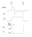
도 1은 종래기술에 따라 오버 드라이빙 방식을 채택한 반도체 메모리 장치의 비트라인 감지증폭기 어레이의 구성을 나타낸 도면이다.1 is a diagram illustrating a configuration of a bit line sense amplifier array of a semiconductor memory device employing an overdriving scheme according to the related art.
도 1을 참조하면, 비트라인 감지증폭기 어레이는 오버 드라이빙의 채택 여부와 관계없이 비트라인 감지증폭기(30)와, 상위 비트라인 분리부(10) 및 하위 비트라인 분리부(50)와, 비트라인 이퀄라이즈/프리차지부(20)와, 컬럼 선택부(40)와, 비트라인 감지증폭기 전원라인 구동부(60)를 포함한다.Referring to FIG. 1, the bit line sense amplifier array may include a bit
여기서, 상위 비트라인 분리부(10)는 상위 분리신호(BISH)에 응답하여 상위 메모리 셀 어레이와 감지증폭기(30)를 분리/연결하기 위한 것이며, 하위 비트라인 분리부(50)는 하위 분리신호(BISL)에 응답하여 하위 메모리 셀 어레이와 감지증폭기(30)를 분리/연결하기 위한 것이다.Here, the upper bit
그리고, 비트라인 감지증폭기(30)는 인에이블 신호가 활성화되어 풀다운 전원라인(통상 SB라 함) 및 풀업 전원라인(RTO)이 예정된 전압 레벨로 구동되면 비트라인 쌍(BL, BLB) - 전하공유 상태로 미세한 전압차를 가짐 - 의 전압차를 감지하여, 하나는 접지전압(VSS)으로 하나는 코어전압(VCORE)으로 증폭한다.When the enable signal is activated and the pull-down power line (commonly referred to as SB) and the pull-up power line (RTO) are driven to a predetermined voltage level, the bit line sense amplifier 30 (BL, BLB)-charge sharing With a slight voltage difference as a state, a voltage difference of-is sensed and one is amplified to ground voltage VSS and one to core voltage VCORE.
또한, 비트라인 이퀄라이즈/프리차지부(20)는 비트라인에 대한 감지/증폭 및 재저장 과정을 종료한 후에 비트라인 이퀄라이즈 신호(BLEQ)에 응답하여 비트라인 쌍(BL, BLB)을 비트라인 프리차지 전압(VBLP) - 통상 VCORE/2 - 으로 프리차지하기 위한 것이다.In addition, the bit line equalizer /
그리고, 컬럼 선택부(40)는 리드 커맨드가 인가되면 컬럼 선택신호(YI)에 응답하여 감지증폭기(30)에 의해 감지/증폭된 데이터를 세그먼트 데이터 버스(SIO, SIOB)에 전달한다.When the read command is applied, the
한편, 비트라인 감지증폭기 전원라인 구동부(60)는 풀업 전원라인 구동 제어신호(SAP)에 응답하여 코어전압단(VCORE)에 걸린 전압으로 RTO 전원라인을 구동하기 위한 NMOS 트랜지스터(M2)와, 풀다운 전원라인 구동 제어신호(SAN)에 응답하여 접지전압(VSS)으로 SB 전원라인을 구동하기 위한 NMOS 트랜지스터(M3)와, 오버 드라이빙 펄스(SAOVDP) - 오버 드라이버 제어신호 - 에 응답하여 RTO 전원라인을 전원전압(VDD)으로 구동하기 위한 NMOS 트랜지스터(M1) - 오버 드라이버 - 와, 비트라인 이퀄라이즈 신호(BLEQ)에 응답하여 비트라인 감지증폭기(30)의 RTO 전원라인 및 SB 전원라인을 비트라인 프리차지 전압(VBLP)으로 프리차지하기 위한 비트라인 감지증폭기(BLSA) 전원라인 이퀄라이즈/프리차지부(62)를 구비한다.On the other hand, the bit line sense amplifier
여기에서는, 오버 드라이빙 펄스(SAOVDP)를 하이 액티브 펄스로 규정하고 오버 드라이버를 NMOS 트랜지스터(M1)로 구현하는 경우를 예시하고 있으나, 오버 드라이버로 PMOS 트랜지스터를 사용할 수도 있다. 풀업 전원라인 구동 제어신호(SAP)에 제어 받는 NMOS 트랜지스터(M2) 역시 마찬가지다.
Here, the case where the over driving pulse SAOVDP is defined as a high active pulse and the over driver is implemented as the NMOS transistor M1 is illustrated. However, the PMOS transistor may be used as the over driver. The same applies to the NMOS transistor M2 controlled by the pull-up power line driving control signal SAP.
도 2는 도 1에 도시된 종래기술에 따른 비트라인 감지증폭기의 전원라인 구동 동작을 설명하기 위해 도시한 타이밍 다이어그램이다.FIG. 2 is a timing diagram illustrating a power line driving operation of the bit line sense amplifier according to the related art shown in FIG. 1.
도 2를 참조하면, 우선 액티브 커맨드(ACT)가 인가되어 워드라인이 활성화되고 셀에 저장된 데이터가 전하공유에 의해 비트라인 쌍(BL, BLB)에 각각 유기된 후, 오버 드라이빙 펄스(SAOVDP)가 로직'하이'(High)로 활성화되고, 풀다운 전원라인 구동 제어신호(SAN)가 로직'하이'(High)로 활성화된다.Referring to FIG. 2, first, an active command ACT is applied to activate a word line, and data stored in a cell is induced in the bit line pairs BL and BLB by charge sharing, and then an overdriving pulse SAOVDP is generated. Logic 'High' is activated, and pull-down power line driving control signal SAN is activated with logic 'High'.
즉, 로직'하이'(High)로 활성화되는 오버 드라이빙 펄스(SAOVDP)에 의해 RTO 전원라인이 외부전원전압(VDD)으로 오버 드라이빙되고, 로직'하이'(High)로 활성화되는 풀다운 전원라인 구동 제어신호(SAN)에 의해 SB 전원라인이 외부접지전압(VSS)으로 드라이빙된다.In other words, the RTO power line is overdriven to the external power supply voltage VDD by the overdrive pulse SAOVDP, which is activated at logic 'high', and the pull-down power line drive control is activated at logic 'high'. The SB power line is driven to the external ground voltage VSS by the signal SAN.
예정된 시간이 흐른 후, 오버 드라이빙 펄스(SAOVDP)가 로직'로우'(Low)로 비활성화되고, 동시에 풀업 전원라인 구동 제어신호(SAP)가 로직'하이'(High)로 활성화되며, 풀다운 전원라인 구동 제어신호(SAN)은 로직'하이'(High)로 활성화 상태를 계속 유지한다.After the predetermined time has elapsed, the overdriving pulse SAOVDP is deactivated to logic 'Low' and at the same time the pull-up power line drive control signal (SAP) is activated to logic 'High' and the pull-down power line is driven. The control signal SAN is maintained at an active state with logic 'high'.
즉, 로직'로우'(Low)로 비활성화되는 오버 드라이빙 펄스(SAOVDP) 및 로직'하이'(High)로 활성화되는 풀업 전원라인 구동 제어신호(SAP)에 의해 RTO 전원라인이 코어전압(VCORE)으로 노말 드라이빙되고, 로직'하이'(High)로 활성화된 상태를 유지하는 풀다운 전원라인 구동 제어신호(SAN)에 의해 SB 전원라인이 외부접지전압(VSS)으로 드라이빙된다.That is, the RTO power line is driven to the core voltage VCORE by the overdrive pulse SAOVDP deactivated by logic 'low' and the pull-up power line drive control signal SAP activated by logic 'high'. The SB power line is driven to the external ground voltage VSS by a pull-down power line driving control signal SAN that is normally driven and maintains a logic 'high' active state.
이후, 일정 시간이 지나면 프리차지 커맨드(PCG)가 인가되어 풀업 및 풀다운 전원라인 구동 제어신호(SAP, SAN)가 비활성화되고 BLSA 전원라인 이퀄라이즈/프리차지부(62)에 의해 RTO 전원라인과 SB 전원라인이 비트라인 프리차지 전압(VBLP) 레벨로 프리차지 된다. 비트라인 프리차지 전압(VBLP)은 통상 VCORE/2 레벨을 가진다.Then, after a predetermined time, the precharge command PCG is applied to deactivate the pull-up and pull-down power line driving control signals SAP and SAN, and the RTO power line and SB by the BLSA power line equalization / precharge unit 62. The power supply line is precharged to the bit line precharge voltage (VBLP) level. The bit line precharge voltage VBLP typically has a VCORE / 2 level.
전술한 바와 같은 방식으로 종래기술에 따른 반도체 메모리 장치의 오버 드라이빙 동작이 이루어지는데, 그 중 RTO 전원라인이 외부전원전압(VDD)으로 오버 드라이빙 구간에서 RTO 전원라인의 전압레벨은 코어전압(VCORE)보다 높은 전압레벨을 갖는 상태가 되지만, RTO 전원라인의 전압레벨이 내부의 셀 어레이에 도달하는 전위량은 RC Delay에 의해 손실을 가지기 때문에 보다 낮은 전압레벨을 가지게 된다.As described above, the overdriving operation of the semiconductor memory device according to the related art is performed, wherein the RTO power line is the external power supply voltage VDD, and the voltage level of the RTO power supply line is the core voltage VCORE in the overdriving period. The voltage level of the RTO power line reaches the internal cell array, but the voltage level of the RTO power line reaches a lower voltage level because of the loss due to the RC delay.
따라서, 오버 드라이빙 펄스(SAOVDP)를 로직'하이'(High)에서 로직'로우'(Low)로 비활성화시키고 풀업 전원전압 드라이빙 펄스(SAP)를 로직'로우'(Low)에서 로직'하이'(High)로 활성화시키는 시점을 결정할 때 주로 셀 어레이의 전압레벨이 코어전압(VCORE)의 전압레벨에 도달하였는지를 기준으로 하게 된다.Therefore, the overdrive pulse SAOVDP is disabled from logic 'high' to logic 'low' and the pull-up supply voltage driving pulse (SAP) is disabled from logic 'low' to logic 'high'. In determining the time point of activation, the reference is mainly based on whether the voltage level of the cell array reaches the voltage level of the core voltage VCORE.
즉, 오버 드라이빙 펄스(SAOVDP)를 로직'하이'(High)에서 로직'로우'(Low)로 비활성화시키고 풀업 전원전압 드라이빙 펄스(SAP)를 로직'로우'(Low)에서 로직'하이'(High)로 활성화시키는 시점이 RTO 전원라인의 전압레벨이 어떤 상태인지와는 상관없이 셀 어레이의 전압레벨이 코어전압(VCORE)에 도달하는 시점을 기준으로 하게 된다.That is, the overdrive pulse SAOVDP is deactivated from logic 'high' to logic 'low' and the pull-up supply voltage driving pulse (SAP) is disabled from logic 'low' to logic 'high'. ) Is based on the time when the voltage level of the cell array reaches the core voltage VCORE, regardless of the state of the voltage level of the RTO power line.
따라서, 오버 드라이빙 펄스(SAOVDP)를 로직'하이'(High)에서 로직'로우'(Low)로 비활성화시키고 풀업 전원전압 드라이빙 펄스(SAP)를 로직'로우'(Low)에서 로직'하이'(High)로 활성화시키는 시점에서 RTO 전원라인의 전압레벨은 코어전압(VCORE)의 전압레벨보다 높은 상태 - 외부전원전압(VDD)의 레벨에 가까움 - 가 된다.Therefore, the overdrive pulse SAOVDP is disabled from logic 'high' to logic 'low' and the pull-up supply voltage driving pulse (SAP) is disabled from logic 'low' to logic 'high'. At the time of activation, the voltage level of the RTO power line becomes higher than the voltage level of the core voltage VCORE, which is close to the level of the external power supply voltage VDD.
이로 인해, RTO 전원라인에서 코어전압(VCORE)단으로 전류가 역류하게 되는 현상이 발생하여 코어전압(VCORE)단의 전압레벨이 상승하게 되며, 이를 보상하기 위해 코어전압(VCORE)을 생성하는 회로에서는 코어전압(VCORE)단의 전압레벨을 방전(Release)하는 동작을 수행하게 문제가 발생한다.As a result, a phenomenon occurs in which current flows backward from the RTO power line to the core voltage VCORE stage, thereby increasing the voltage level of the core voltage VCORE stage, and generating a core voltage VCORE to compensate for this. In this case, a problem arises in that an operation of discharging the voltage level of the core voltage VCORE stage is performed.
전술한 바와 같은 일련의 동작을 하는 동안에 반도체 메모리 장치 내부의 코어전압(VCORE)을 생성하는 회로에서 발생하는 노이즈(noise) 및 전류의 손실은 반도체 메모리 장치 전체의 퍼포먼스저하로 이어지게 된다.
During a series of operations as described above, the loss of noise and current generated in a circuit that generates the core voltage VCORE inside the semiconductor memory device leads to a decrease in performance of the entire semiconductor memory device.
본 발명은 전술한 종래기술의 문제점을 해결하기 위해 제안된 것으로서, 오버 드라이빙 동작으로 인해 소모되는 전류량을 최소한으로 유지하는 반도체 메모리 장치를 제공하는데 그 목적이 있다.
SUMMARY OF THE INVENTION The present invention has been proposed to solve the above-mentioned problems of the prior art, and an object thereof is to provide a semiconductor memory device which maintains a minimum amount of current consumed due to an overdriving operation.
상기의 해결하고자 하는 과제를 달성하기 위한 본 발명의 일 측면에 따르면, 비트 라인에 실린 데이터를 감지증폭하기 위한 비트 라인 감지증폭부; 감지증폭 인에이블 신호에 응답하여 순차적으로 오버 드라이빙 신호와 노말 드라이빙 신호를 생성하되, 상기 오버 드라이빙 신호의 활성화구간과 상기 노말 드라이빙 신호의 활성화구간이 예정된 제1 시간만큼 차이를 갖도록 하는 드라이빙 신호 생성부; 및 상기 오버 드라이빙 신호의 활성화구간에서 상기 비트 라인 감지증폭부의 전원라인을 외부전원전압으로 구동하고, 상기 노말 드라이빙 신호의 활성화구간에서 상기 비트 라인 감지증폭부의 전원라인을 코어전압으로 구동하는 전원라인 구동부를 구비하는 반도체 메모리 장치를 제공한다.
According to an aspect of the present invention for achieving the above object to be solved, the bit line sense amplifier for sensing and amplifying data carried on the bit line; A driving signal generator configured to sequentially generate an overdriving signal and a normal driving signal in response to the detection amplification enable signal, so that an activation section of the overdriving signal and an activation section of the normal driving signal differ by a predetermined first time. ; And a power line driver driving the power line of the bit line detection amplifier part to an external power supply voltage during an activation period of the overdriving signal, and driving the power line of the bit line detection amplifier part to a core voltage in an activation period of the normal driving signal. It provides a semiconductor memory device having a.
전술한 본 발명은 RTO 전원라인을 오버 드라이빙하는 과정에서 RTO 전원라인에 어떠한 전원전압도 공급되는 않는 예정된 제1 시간(tVDLY)이 존재하도록 제어함으로써 RTO 전원라인이 외부전원전압(VDD)의 전압레벨에서 코어전압(VCORE)의 전압레벨로 완만하게 변동하도록 한다.The present invention described above controls the voltage level of the external power supply voltage (VDD) by controlling the RTO power supply line to have a predetermined first time tVDLY in which no power supply voltage is supplied to the RTO power supply line in the course of overdriving the RTO power supply line. The voltage fluctuates slowly to the voltage level of the core voltage VCORE at.
따라서, RTO 전원라인과 코어전압(VCORE)단 사이에 전압레벨 차이가 거의 없는 상태에서 코어전압(VCORE)으로 RTO 전원라인을 구동하게 되며, RTO 전원라인에서 코어전압(VCORE)단으로 역류하는 전류의 양을 최소한으로 유지하는 것이 효과가 있다.Therefore, the RTO power line is driven with the core voltage VCORE in a state where there is almost no difference in voltage level between the RTO power line and the core voltage VCORE stage, and the current flowing back from the RTO power line to the core voltage VCORE stage. Keeping the amount to a minimum is effective.
이로 인해, 오버 드라이빙 동작이 수행될 때에도 코어전압(VCORE)을 생성하는 회로의 동작을 충분히 안정화시켜 노이즈(noise)의 발생을 최소화하고 소모되는 전류의 크기를 최소화 할 수 있도록 하는 효과가 있다.
Therefore, even when the overdriving operation is performed, the operation of the circuit generating the core voltage VCORE is sufficiently stabilized, thereby minimizing the occurrence of noise and minimizing the amount of current consumed.
도 1은 종래기술에 따라 오버 드라이빙 방식을 채택한 반도체 메모리 장치의 비트라인 감지증폭기 어레이의 구성을 나타낸 도면.
도 2는 도 1에 도시된 종래기술에 따른 비트라인 감지증폭기의 전원라인 구동 동작을 설명하기 위해 도시한 타이밍 다이어그램.
도 3은 본 발명의 실시예에 따라 오버 드라이빙 방식을 채택한 반도체 메모리 장치의 비트라인 감지증폭기 어레이의 구성을 나타낸 도면.
도 4 및 도 5는 도 3에 도시된 본 발명의 실시예에 따른 비트라인 감지증폭기의 전원라인 구동 동작을 설명하기 위해 도시한 타이밍 다이어그램.1 is a diagram illustrating a configuration of a bit line sense amplifier array of a semiconductor memory device employing an overdriving scheme according to the related art.
2 is a timing diagram illustrating a power line driving operation of a bit line sense amplifier according to the related art shown in FIG.
3 is a diagram illustrating a configuration of an array of bit line sense amplifiers of a semiconductor memory device employing an overdriving scheme according to an exemplary embodiment of the present invention.
4 and 5 are timing diagrams for explaining a power line driving operation of the bit line sense amplifier according to the embodiment of the present invention shown in FIG.
이하, 첨부된 도면을 참조하여 본 발명의 바람직한 실시예를 설명하기로 한다. 그러나, 본 발명은 이하에서 개시되는 실시예에 한정되는 것이 아니라 서로 다른 다양한 형태로 구성될 수 있으며, 단지 본 실시예는 본 발명의 개시가 완전하도록하며 통상의 지식을 가진자에게 본 발명의 범주를 완전하게 알려주기 위해 제공되는 것이다.
Hereinafter, preferred embodiments of the present invention will be described with reference to the accompanying drawings. However, the present invention is not limited to the embodiments disclosed below, but may be configured in various different forms, only this embodiment is intended to complete the disclosure of the present invention and to those skilled in the art the scope of the present invention It is provided to inform you completely.
도 3은 본 발명의 실시예에 따라 오버 드라이빙 방식을 채택한 반도체 메모리 장치의 비트라인 감지증폭기 어레이의 구성을 나타낸 도면이다.3 is a block diagram illustrating a configuration of an array of bit line sense amplifiers of a semiconductor memory device employing an overdriving scheme according to an exemplary embodiment of the present invention.
도 3을 참조하면, 본 발명의 실시예에 따른 비트라인 감지증폭기는, 비트 라인(BL, BLB)에 실린 데이터를 감지증폭하기 위한 비트 라인 감지증폭부(360)와, 감지증폭 인에이블 신호(SAEN)에 응답하여 순차적으로 오버 드라이빙 신호(SAOVDP)와 노말 드라이빙 신호(SAP)를 생성하되, 오버 드라이빙 신호(SAOVDP)의 활성화구간과 노말 드라이빙 신호(SAP)의 활성화구간이 예정된 제1 시간(tVDLY)만큼 차이를 갖도록 하는 드라이빙 신호 생성부(300), 및 오버 드라이빙 신호(SAOVDP)의 활성화구간에서 비트 라인 감지증폭부(360)의 RTO 전원라인을 외부전원전압(VDD)으로 구동하고, 노말 드라이빙 신호(SAP)의 활성화구간에서 비트 라인 감지증폭부(360)의 RTO 전원라인을 코어전압(VCORE)으로 구동하는 전원라인 구동부(320)를 구비한다.Referring to FIG. 3, a bit line sense amplifier according to an embodiment of the present invention includes a bit
여기서, 드라이빙 신호 생성부(300)는, 감지증폭 인에이블 신호(SAEN)에 응답하여 제1 제어신호(SAE_P)를 생성하고, 제1 제어신호(SAE_P)를 예정된 제2 시간(tSDLY)만큼 지연시켜 제2 제어신호(SAE_O)를 생성하며, 제2 제어신호(SAE_O)를 예정된 제1 시간(tVDLY)만큼 지연시켜 제3 제어신호(SAE_C)를 생성하는 드라이빙 제어신호 생성부(302), 및 제1 제어신호(SAE_P)에 응답하여 오버 드라이빙 신호(SAOVDP)를 활성화시키고 제2 제어신호(SAE_O)에 응답하여 오버 드라이빙 신호(SAOVDP)를 비활성화시키며 제3 제어신호(SAE_C)에 응답하여 노말 드라이빙 신호(SAP)를 활성화시키는 드라이빙 신호 활성화 제어부(304)를 구비한다.Here, the driving
또한, 드라이빙 제어신호 생성부(302)는, 감지증폭 인에이블 신호(SAEN)가 활성화되는 것에 응답하여 제1 제어신호(SAE_P)를 활성화시키기 위한 제어신호 출력부(3022)와, 제1 제어신호(SAE_P)를 예정된 제1 시간(tVDLY)만큼 지연시켜 제3 제어신호(SAE_C)로서 출력하기 위한 제1 지연부(3024), 및 제1 제어신호(SAE_P)를 예정된 제2 시간(tSDLY)만큼 지연시켜 제2 제어신호(SAE_O)로서 출력하기 위한 제2 지연부(3026)를 구비한다.In addition, the driving
그리고, 드라이빙 신호 활성화 제어부(304)는, 제1 제어신호(SAE_P)와 제2 제어신호(SAE_O)를 입력받아 논리곱 연산을 수행하여 오버 드라이빙 신호(SAOVDP)로서 출력하기 위한 낸드게이트(ND1) 및 인버터(INV1)와, 오버 드라이빙 신호(SAOVDP)와 제3 제어신호(SAE_C)를 입력받아 부정 논리합 연산을 수행하여 노말 드라이빙 신호(SAP)로서 출력하기 위한 노아게이트(NOR1)를 구비한다.The driving signal
또한, 드라이빙 제어신호 생성부(302)는, 테스트 신호(TM)에 응답하여 예정된 제1 시간(tVDLY)의 크기를 조절하는 것이 가능하다. 즉, 드라이빙 제어신호 생성부(302)의 구성요소 중 제1 지연부(3024)의 지연량(tVDLY)을 테스트 신호(TM)에 따라 조절하는 것이 가능하다. 예컨대, 제1 지연부(3024)는 테스트 신호(TM)가 활성화될 때 제1 제어신호(SAE_P)를 예정된 제1 시간(tVDLY)만큼 지연시켜 제3 제어신호(SAE_C)로서 출력하고, 비활성화될 때 제1 제어신호(SAE_P)를 지연시키지 않고 그대로 제3 제어신호(SAE_C)로서 출력하도록 제어되는 것이 가능하다.In addition, the driving
참고로, 제어신호 출력부(3022)는 감지증폭 인에이블 신호(SAEN)가 활성화되는 구간동안 활성화상태를 유지하는 풀다운 노말 드라이빙 신호(SAN)도 생성한다. 즉, 풀다운 노말 드라이빙 신호(SAN)는 종래기술에서 설명했던 '풀다운 전원라인 구동 제어신호(SAN)'와 완전히 동일한 신호이다. 따라서, SB 전원라인은 종래기술에서와 마찬가지로 외부접지전압(VSS)으로 드라이빙 된다.
For reference, the control
도 4는 도 3에 도시된 본 발명의 실시예에 따른 비트라인 감지증폭기의 전원라인 구동 동작을 설명하기 위해 도시한 타이밍 다이어그램이다.4 is a timing diagram illustrating a power line driving operation of the bit line sense amplifier according to the embodiment of the present invention shown in FIG.
도 4를 참조하면, 우선 액티브 커맨드(ACT)가 인가되어 워드라인이 활성화되고 셀에 저장된 데이터가 전하공유에 의해 비트라인(BL, BLB)에 각각 유기된 후, 오버 드라이빙 신호(SAOVDP)가 로직'하이'(High)로 활성화되고, 풀다운 노말 드라이빙 신호(SAN)가 로직'하이'(High)로 활성화된다.Referring to FIG. 4, first, an active command ACT is applied to activate a word line, and data stored in a cell is induced on the bit lines BL and BLB by charge sharing, respectively, and then the overdriving signal SAOVDP is logic. 'High' is activated, and the pull-down normal driving signal (SAN) is activated at logic 'High'.
즉, 로직'하이'(High)로 활성화되는 오버 드라이빙 신호(SAOVDP)에 의해 RTO 전원라인이 외부전원전압(VDD)으로 오버 드라이빙되고, 로직'하이'(High)로 활성화되는 풀다운 전원라인 구동 제어신호(SAN)에 의해 SB 전원라인이 외부접지전압(VSS)으로 드라이빙된다.In other words, the RTO power line is overdriven to the external power supply voltage VDD by the overdrive signal SAOVDP, which is activated at logic 'high', and the pull-down power line drive control is activated at logic 'high'. The SB power line is driven to the external ground voltage VSS by the signal SAN.
예정된 제2 시간(tSDLY)이 흐른 후, 오버 드라이빙 신호(SAOVDP)가 로직'로우'(Low)로 비활성화되더라도 노말 드라이빙 신호(SAP)는 로직'로우'(Low)로 비활성화된 상태를 유지한다.After the second predetermined time tSDLY passes, the normal driving signal SAP remains inactivated to the logic 'low' even if the overdriving signal SAOVDP is deactivated to the logic 'low'.
예정된 제1 시간(tVDLY)이 흐른 후, 오버 드라이빙 펄스(SAOVDP)는 계속 로직'로우'(Low)로 비활성화된 상태를 유지하고, 노말 드라이빙 신호(SAP)가 로직'하이'(High)로 활성화된다.After the first predetermined time tVDLY has passed, the overdriving pulse SAOVDP continues to be deactivated to logic 'low', and the normal driving signal SAP is activated to logic 'high'. do.
따라서, RTO 전원라인에는 예정된 제1 시간(tVDLY)동안 외부전원전압(VDD)단으로부터 전하를 공급받지도 않고 코어전압(VCORE)단으로부터 전하를 공급받지도 않는다. 때문에, 도면에 도시된 것처럼 오버 드라이빙 신호(SAOVDP)가 로직'로우'(Low)로 비활성화되는 시점에서부터 RTO 전원라인의 전압레벨이 천천히 하강 - 외부전원전압(VDD)의 레벨에서 코어전압(VCORE)의 레벨로 하강함 - 하다가 노말 드라이빙 신호(SAP)가 로직'하이'(High)로 활성화될 때 완전히 코어전압(VCORE)의 레벨과 동일한 상태가 된다.Therefore, the RTO power line does not receive charge from the external power supply voltage VDD terminal or charge from the core voltage VCORE terminal for the first predetermined time tVDLY. Therefore, as shown in the figure, the voltage level of the RTO power line slowly drops from the time when the overdriving signal SAOVDP is deactivated to logic 'low'-the core voltage VCORE at the level of the external power supply voltage VDD. Descends to the level of-When the normal driving signal SAP is activated to logic 'high', it is completely at the same level as the core voltage VCORE.
이와 같이 RTO 전원라인의 레벨이 변동하고 있는 과정에서도 풀다운 노말 드라이빙 신호(SAN)는 로직'하이'(High)로 활성화된 상태를 유지하므로 SB 전원라인은 외부접지전압(VSS)으로 드라이빙된 상태를 유지하게 된다.In this process, the pull-down normal driving signal (SAN) remains active at logic 'high' even when the level of the RTO power line is changing. Therefore, the SB power line is driven by the external ground voltage (VSS). Will be maintained.
이후, 일정 시간이 지나면 프리차지 커맨드(PCG)가 인가되어 풀업 및 풀다운 전원라인 구동 제어신호(SAP, SAN)가 비활성화되고 BLSA 전원라인 이퀄라이즈/프리차지부(62)에 의해 RTO 전원라인과 SB 전원라인이 비트라인 프리차지 전압(VBLP) 레벨로 프리차지 된다. 비트라인 프리차지 전압(VBLP)은 통상 VCORE/2 레벨을 가진다.Then, after a predetermined time, the precharge command PCG is applied to deactivate the pull-up and pull-down power line driving control signals SAP and SAN, and the RTO power line and SB by the BLSA power line equalization / precharge unit 62. The power supply line is precharged to the bit line precharge voltage (VBLP) level. The bit line precharge voltage VBLP typically has a VCORE / 2 level.
전술한 바와 같은 방식으로 본 발명의 실시예에 따른 반도체 메모리 장치의 오버 드라이빙 동작이 이루어지는데, 그 중 RTO 전원라인이 외부전원전압(VDD)의 전압레벨로 오버 드라이빙 된 후 코어전압(VCORE)의 전압레벨로 노말 드라이빙 되는 과정이 종래기술에 비해 완만하게 이루어지는 것을 알 수 있다. 이는, RTO 전원라인에 어떠한 전원전압도 공급되는 않는 예정된 제1 시간(tVDLY)이 존재하기 때문에 RTO 전원라인에서 셀 어레이까지의 로딩(loading)이 차지 쉐어링(charge sharing)되는 시간을 충분히 갖게 되면서 발생하는 현상이다.As described above, an overdriving operation of the semiconductor memory device according to an exemplary embodiment of the present invention is performed, in which the RTO power line is overdriven to a voltage level of the external power supply voltage VDD, and then the It can be seen that the normal driving process at a voltage level is smoother than in the prior art. This occurs because there is a predetermined first time tVDLY in which no power voltage is supplied to the RTO power line, so that the loading from the RTO power line to the cell array has sufficient time for charge sharing. It is a phenomenon.
따라서, 노말 드라이빙 신호(SAP)가 로직'하이'(High)로 활성화되는 시점에서 RTO 전원라인의 전압레벨은 종래기술에 비해 충분히 낮은 상태가 된다는 것을 알 수 있다. 이로 인해, RTO 전원라인과 코어전압(VCORE)단 사이에 전압레벨 차이가 거의 없는 상태가 될 수 있으며, 따라서, RTO 전원라인에서 코어전압(VCORE)단으로 역류하는 전류의 양을 최소한으로 유지하는 것이 가능하고, 코어전압(VCORE)단의 전압레벨이 상승하는 것을 최소한으로 유지하는 것이 가능하다. 즉, 오버 드라이빙 동작으로 인해 코어전압(VCORE)을 생성하는 회로에서 코어전압(VCORE)단의 전압레벨을 방전(Release)하는 동작이 발생하는 것을 최소화할 수 있으며, 이는, 코어전압(VCORE)을 생성하는 회로의 동작을 안정화시켜 노이즈(noise)의 발생을 최소화하고 소모되는 전류의 크기를 최소화 할 수 있도록 한다.Accordingly, it can be seen that the voltage level of the RTO power line is sufficiently low compared to the prior art when the normal driving signal SAP is activated at logic 'high'. As a result, there may be almost no voltage level difference between the RTO power line and the core voltage VCORE stage. Therefore, the amount of current flowing back from the RTO power line to the core voltage VCORE stage is kept to a minimum. It is possible to keep the voltage level at the core voltage VCORE stage rise to a minimum. That is, in the circuit which generates the core voltage VCORE due to the overdriving operation, an operation of releasing the voltage level of the core voltage VCORE stage may be minimized, which may reduce the core voltage VCORE. By stabilizing the operation of the circuit to be generated to minimize the occurrence of noise (noise) and to minimize the amount of current consumed.
또한, 본 발명의 실시예에 따른 반도체 메모리 장치의 오버 드라이빙 동작이 도 5와 같이 되도록 제어하는 것도 가능하다.In addition, it is also possible to control the overdriving operation of the semiconductor memory device according to the embodiment of the present invention as shown in FIG. 5.
즉, 오버 드라이빙 신호(SAOVDP)의 활성화구간 길이에 대응하는 예정된 제2 시간(tSDLY)의 길이를 도 4에 도시된 제어동작보다 더 감소시켜 외부전원전압(VDD)단에서 RTO 전원라인으로 공급되는 전류의 크기를 도 4에 도시된 제어동작보다 더 감소시키고, 동시에 RTO 전원라인의 전압레벨이 외부전원전압(VDD)의 전압레벨에서 코어전압(VCORE)의 전압레벨로 변동해가는 과정이 도 4에 도시된 제어동작보다 더 완만해지도록 할 수 있다.That is, the length of the second predetermined time tSDLY corresponding to the length of the activation period of the overdriving signal SAOVDP is further reduced than the control operation shown in FIG. 4 to be supplied from the external power supply voltage VDD to the RTO power line. The process of reducing the magnitude of the current more than the control operation shown in FIG. 4 and simultaneously changing the voltage level of the RTO power line from the voltage level of the external power supply voltage VDD to the voltage level of the core voltage VCORE is shown in FIG. 4. It can be made more gentle than the control operation shown in.
이렇게, 도 5에 도시된 것과 같이 본 발명의 실시예에 따른 반도체 메모리 장치의 오버 드라이빙 동작을 제어하게 될 경우, 도 4에 도시된 제어동작보다 좀 더 전류소모를 줄이는 것이 가능하다.
As such, when the overdriving operation of the semiconductor memory device according to the exemplary embodiment of the present invention is controlled as shown in FIG. 5, it is possible to reduce the current consumption more than the control operation shown in FIG. 4.
이상에서 설명한 본 발명은 전술한 실시예 및 첨부된 도면에 의해 한정되는 것이 아니고, 본 발명의 기술적 사상을 벗어나지 않는 범위 내에서 여러 가지 치환, 변형 및 변경이 가능하다는 것이 본 발명이 속한 기술분야에서 통상의 지식을 가진자에게 있어 명백할 것이다.The present invention described above is not limited to the above-described embodiments and the accompanying drawings, and various substitutions, modifications, and changes are possible in the art without departing from the technical spirit of the present invention. It will be apparent to those of ordinary skill.
예컨대, 전술한 실시예에서 예시한 논리 게이트 및 트랜지스터는 입력되는 신호의 극성에 따라 그 위치 및 종류가 다르게 구현되어야 할 것이다.
For example, the logic gate and the transistor illustrated in the above-described embodiment should be implemented differently in position and type depending on the polarity of the input signal.
300 : 드라이빙 신호 생성부
320 : 전원라인 구동부
360 : 비트라인 감지증폭부300: driving signal generation unit
320: power line drive unit
360: bit line detection amplifier
Claims (3)
Translated fromKorean감지증폭 인에이블 신호에 응답하여 순차적으로 오버 드라이빙 신호와 노말 드라이빙 신호를 생성하되, 상기 오버 드라이빙 신호의 활성화구간과 상기 노말 드라이빙 신호의 활성화구간이 예정된 제1 시간만큼 차이를 갖도록 하는 드라이빙 신호 생성부; 및
상기 오버 드라이빙 신호의 활성화구간에서 상기 비트 라인 감지증폭부의 전원라인을 외부전원전압으로 구동하고, 상기 노말 드라이빙 신호의 활성화구간에서 상기 비트 라인 감지증폭부의 전원라인을 코어전압으로 구동하는 전원라인 구동부
를 구비하는 반도체 메모리 장치.
A bit line sense amplifier configured to sense and amplify data carried on the bit line;
A driving signal generator configured to sequentially generate an overdriving signal and a normal driving signal in response to the detection amplification enable signal, so that an activation section of the overdriving signal and an activation section of the normal driving signal differ by a predetermined first time. ; And
A power line driver for driving the power line of the bit line detection amplifier part with an external power supply voltage in an activation period of the overdriving signal, and driving the power line of the bit line detection amplifier part with a core voltage in an activation period of the normal driving signal;
And the semiconductor memory device.
상기 드라이빙 신호 생성부는,
상기 감지증폭 인에이블 신호에 응답하여 제1 제어신호를 생성하고, 상기 제1 제어신호를 예정된 제2 시간만큼 지연시켜 제2 제어신호를 생성하며, 상기 제2 제어신호를 상기 예정된 제1 시간만큼 지연시켜 제3 제어신호를 생성하는 드라이빙 제어신호 생성부; 및
상기 제1 및 제2 제어신호에 응답하여 상기 오버 드라이빙 신호를 활성화 및 비활성화시키고, 상기 제3 제어신호에 응답하여 상기 노말 드라이빙 신호를 활성화시키는 드라이빙 신호 활성화 제어부를 구비하는 것을 특징으로 하는 반도체 메모리 장치.
The method of claim 1,
The driving signal generator,
A first control signal is generated in response to the sensing amplification enable signal, a second control signal is generated by delaying the first control signal by a predetermined second time, and the second control signal is generated by the predetermined first time. A driving control signal generator configured to delay and generate a third control signal; And
And a driving signal activation controller configured to activate and deactivate the overdriving signal in response to the first and second control signals, and to activate the normal driving signal in response to the third control signal. .
상기 드라이빙 제어신호 생성부는,
테스트 신호에 응답하여 상기 예정된 제1 시간의 크기를 조절하는 것을 특징으로 하는 반도체 메모리 장치.The method of claim 2,
The driving control signal generator,
And adjusting the size of the predetermined first time in response to a test signal.
Priority Applications (1)
| Application Number | Priority Date | Filing Date | Title |
|---|---|---|---|
| KR1020100129687AKR20120068186A (en) | 2010-12-17 | 2010-12-17 | Semiconductor memory device |
Applications Claiming Priority (1)
| Application Number | Priority Date | Filing Date | Title |
|---|---|---|---|
| KR1020100129687AKR20120068186A (en) | 2010-12-17 | 2010-12-17 | Semiconductor memory device |
Publications (1)
| Publication Number | Publication Date |
|---|---|
| KR20120068186Atrue KR20120068186A (en) | 2012-06-27 |
Family
ID=46686935
Family Applications (1)
| Application Number | Title | Priority Date | Filing Date |
|---|---|---|---|
| KR1020100129687AWithdrawnKR20120068186A (en) | 2010-12-17 | 2010-12-17 | Semiconductor memory device |
Country Status (1)
| Country | Link |
|---|---|
| KR (1) | KR20120068186A (en) |
- 2010
- 2010-12-17KRKR1020100129687Apatent/KR20120068186A/ennot_activeWithdrawn
Similar Documents
| Publication | Publication Date | Title |
|---|---|---|
| JP4993912B2 (en) | Semiconductor memory device and method for driving bit line sense amplifier of semiconductor memory device | |
| US8339872B2 (en) | Semiconductor memory apparatus and method of driving bit-line sense amplifier | |
| JP5595236B2 (en) | Semiconductor device | |
| KR101175249B1 (en) | Semiconductor memory device and operation method thereof | |
| US20070153592A1 (en) | Over driving control signal generator in semiconductor memory device | |
| KR20160124582A (en) | Sense amplifier and semiconductor device including the same | |
| KR20170055596A (en) | Semiconductor device | |
| KR100625793B1 (en) | Semiconductor memory device | |
| KR20160069218A (en) | Semiconductor memory device | |
| KR20160148346A (en) | Sense amplifier driving device and semiconductor device including the same | |
| KR100546188B1 (en) | Semiconductor memory device having a sense amplifier and method for over driving its sense amplifier | |
| KR20110025487A (en) | Semiconductor memory device | |
| KR100780633B1 (en) | Over driver control signal generation circuit of semiconductor memory device | |
| KR102468819B1 (en) | Semiconductor memory device and operating method thereof | |
| KR100838364B1 (en) | Amplification Enable Signal Generation Circuit of Semiconductor Memory Device | |
| KR101470529B1 (en) | Semiconductor memory device and method of controlling the sense amplifier of the device | |
| KR100892727B1 (en) | Semiconductor memory device and bitline sensing amplification method thereof | |
| US20080079472A1 (en) | Over driver control signal generator in semiconductor memory device | |
| KR20190063885A (en) | Semiconductor Memory Apparatus | |
| US20080080273A1 (en) | Over-drive control signal generator for use in semiconductor memory device | |
| KR102034614B1 (en) | Semiconductor memory device | |
| KR100612951B1 (en) | Semiconductor memory device | |
| KR20120068186A (en) | Semiconductor memory device | |
| KR100855275B1 (en) | Semiconductor memory device including sense amplifier controller | |
| KR100780634B1 (en) | Over driver control signal generation circuit of semiconductor memory device |
Legal Events
| Date | Code | Title | Description |
|---|---|---|---|
| PA0109 | Patent application | Patent event code:PA01091R01D Comment text:Patent Application Patent event date:20101217 | |
| PG1501 | Laying open of application | ||
| PC1203 | Withdrawal of no request for examination | ||
| WITN | Application deemed withdrawn, e.g. because no request for examination was filed or no examination fee was paid |