KR20120067525A - Semiconductor device and method of manufacturing the same - Google Patents
Semiconductor device and method of manufacturing the sameDownload PDFInfo
- Publication number
- KR20120067525A KR20120067525AKR20100128972AKR20100128972AKR20120067525AKR 20120067525 AKR20120067525 AKR 20120067525AKR 20100128972 AKR20100128972 AKR 20100128972AKR 20100128972 AKR20100128972 AKR 20100128972AKR 20120067525 AKR20120067525 AKR 20120067525A
- Authority
- KR
- South Korea
- Prior art keywords
- pattern
- insulating layer
- substrate
- opening
- electrode
- Prior art date
- Legal status (The legal status is an assumption and is not a legal conclusion. Google has not performed a legal analysis and makes no representation as to the accuracy of the status listed.)
- Withdrawn
Links
Images


Classifications
- H—ELECTRICITY
- H01—ELECTRIC ELEMENTS
- H01L—SEMICONDUCTOR DEVICES NOT COVERED BY CLASS H10
- H01L21/00—Processes or apparatus adapted for the manufacture or treatment of semiconductor or solid state devices or of parts thereof
- H01L21/70—Manufacture or treatment of devices consisting of a plurality of solid state components formed in or on a common substrate or of parts thereof; Manufacture of integrated circuit devices or of parts thereof
- H01L21/71—Manufacture of specific parts of devices defined in group H01L21/70
- H01L21/768—Applying interconnections to be used for carrying current between separate components within a device comprising conductors and dielectrics
- H01L21/76898—Applying interconnections to be used for carrying current between separate components within a device comprising conductors and dielectrics formed through a semiconductor substrate
- H—ELECTRICITY
- H01—ELECTRIC ELEMENTS
- H01L—SEMICONDUCTOR DEVICES NOT COVERED BY CLASS H10
- H01L21/00—Processes or apparatus adapted for the manufacture or treatment of semiconductor or solid state devices or of parts thereof
- H01L21/70—Manufacture or treatment of devices consisting of a plurality of solid state components formed in or on a common substrate or of parts thereof; Manufacture of integrated circuit devices or of parts thereof
- H01L21/71—Manufacture of specific parts of devices defined in group H01L21/70
- H01L21/768—Applying interconnections to be used for carrying current between separate components within a device comprising conductors and dielectrics
- H01L21/76801—Applying interconnections to be used for carrying current between separate components within a device comprising conductors and dielectrics characterised by the formation and the after-treatment of the dielectrics, e.g. smoothing
- H01L21/7682—Applying interconnections to be used for carrying current between separate components within a device comprising conductors and dielectrics characterised by the formation and the after-treatment of the dielectrics, e.g. smoothing the dielectric comprising air gaps
- H—ELECTRICITY
- H01—ELECTRIC ELEMENTS
- H01L—SEMICONDUCTOR DEVICES NOT COVERED BY CLASS H10
- H01L23/00—Details of semiconductor or other solid state devices
- H01L23/48—Arrangements for conducting electric current to or from the solid state body in operation, e.g. leads, terminal arrangements ; Selection of materials therefor
- H01L23/481—Internal lead connections, e.g. via connections, feedthrough structures
- H—ELECTRICITY
- H01—ELECTRIC ELEMENTS
- H01L—SEMICONDUCTOR DEVICES NOT COVERED BY CLASS H10
- H01L25/00—Assemblies consisting of a plurality of semiconductor or other solid state devices
- H01L25/03—Assemblies consisting of a plurality of semiconductor or other solid state devices all the devices being of a type provided for in a single subclass of subclasses H10B, H10D, H10F, H10H, H10K or H10N, e.g. assemblies of rectifier diodes
- H01L25/04—Assemblies consisting of a plurality of semiconductor or other solid state devices all the devices being of a type provided for in a single subclass of subclasses H10B, H10D, H10F, H10H, H10K or H10N, e.g. assemblies of rectifier diodes the devices not having separate containers
- H01L25/065—Assemblies consisting of a plurality of semiconductor or other solid state devices all the devices being of a type provided for in a single subclass of subclasses H10B, H10D, H10F, H10H, H10K or H10N, e.g. assemblies of rectifier diodes the devices not having separate containers the devices being of a type provided for in group H10D89/00
- H01L25/0657—Stacked arrangements of devices
- H—ELECTRICITY
- H01—ELECTRIC ELEMENTS
- H01L—SEMICONDUCTOR DEVICES NOT COVERED BY CLASS H10
- H01L21/00—Processes or apparatus adapted for the manufacture or treatment of semiconductor or solid state devices or of parts thereof
- H01L21/70—Manufacture or treatment of devices consisting of a plurality of solid state components formed in or on a common substrate or of parts thereof; Manufacture of integrated circuit devices or of parts thereof
- H01L21/71—Manufacture of specific parts of devices defined in group H01L21/70
- H01L21/768—Applying interconnections to be used for carrying current between separate components within a device comprising conductors and dielectrics
- H01L21/76801—Applying interconnections to be used for carrying current between separate components within a device comprising conductors and dielectrics characterised by the formation and the after-treatment of the dielectrics, e.g. smoothing
- H01L21/76829—Applying interconnections to be used for carrying current between separate components within a device comprising conductors and dielectrics characterised by the formation and the after-treatment of the dielectrics, e.g. smoothing characterised by the formation of thin functional dielectric layers, e.g. dielectric etch-stop, barrier, capping or liner layers
- H01L21/76831—Applying interconnections to be used for carrying current between separate components within a device comprising conductors and dielectrics characterised by the formation and the after-treatment of the dielectrics, e.g. smoothing characterised by the formation of thin functional dielectric layers, e.g. dielectric etch-stop, barrier, capping or liner layers in via holes or trenches, e.g. non-conductive sidewall liners
- H—ELECTRICITY
- H01—ELECTRIC ELEMENTS
- H01L—SEMICONDUCTOR DEVICES NOT COVERED BY CLASS H10
- H01L2224/00—Indexing scheme for arrangements for connecting or disconnecting semiconductor or solid-state bodies and methods related thereto as covered by H01L24/00
- H01L2224/01—Means for bonding being attached to, or being formed on, the surface to be connected, e.g. chip-to-package, die-attach, "first-level" interconnects; Manufacturing methods related thereto
- H01L2224/02—Bonding areas; Manufacturing methods related thereto
- H01L2224/04—Structure, shape, material or disposition of the bonding areas prior to the connecting process
- H01L2224/0401—Bonding areas specifically adapted for bump connectors, e.g. under bump metallisation [UBM]
- H—ELECTRICITY
- H01—ELECTRIC ELEMENTS
- H01L—SEMICONDUCTOR DEVICES NOT COVERED BY CLASS H10
- H01L2224/00—Indexing scheme for arrangements for connecting or disconnecting semiconductor or solid-state bodies and methods related thereto as covered by H01L24/00
- H01L2224/01—Means for bonding being attached to, or being formed on, the surface to be connected, e.g. chip-to-package, die-attach, "first-level" interconnects; Manufacturing methods related thereto
- H01L2224/02—Bonding areas; Manufacturing methods related thereto
- H01L2224/04—Structure, shape, material or disposition of the bonding areas prior to the connecting process
- H01L2224/04042—Bonding areas specifically adapted for wire connectors, e.g. wirebond pads
- H—ELECTRICITY
- H01—ELECTRIC ELEMENTS
- H01L—SEMICONDUCTOR DEVICES NOT COVERED BY CLASS H10
- H01L2224/00—Indexing scheme for arrangements for connecting or disconnecting semiconductor or solid-state bodies and methods related thereto as covered by H01L24/00
- H01L2224/01—Means for bonding being attached to, or being formed on, the surface to be connected, e.g. chip-to-package, die-attach, "first-level" interconnects; Manufacturing methods related thereto
- H01L2224/02—Bonding areas; Manufacturing methods related thereto
- H01L2224/04—Structure, shape, material or disposition of the bonding areas prior to the connecting process
- H01L2224/05—Structure, shape, material or disposition of the bonding areas prior to the connecting process of an individual bonding area
- H01L2224/05001—Internal layers
- H01L2224/05005—Structure
- H01L2224/05009—Bonding area integrally formed with a via connection of the semiconductor or solid-state body
- H—ELECTRICITY
- H01—ELECTRIC ELEMENTS
- H01L—SEMICONDUCTOR DEVICES NOT COVERED BY CLASS H10
- H01L2224/00—Indexing scheme for arrangements for connecting or disconnecting semiconductor or solid-state bodies and methods related thereto as covered by H01L24/00
- H01L2224/01—Means for bonding being attached to, or being formed on, the surface to be connected, e.g. chip-to-package, die-attach, "first-level" interconnects; Manufacturing methods related thereto
- H01L2224/02—Bonding areas; Manufacturing methods related thereto
- H01L2224/04—Structure, shape, material or disposition of the bonding areas prior to the connecting process
- H01L2224/06—Structure, shape, material or disposition of the bonding areas prior to the connecting process of a plurality of bonding areas
- H01L2224/061—Disposition
- H01L2224/0618—Disposition being disposed on at least two different sides of the body, e.g. dual array
- H01L2224/06181—On opposite sides of the body
- H—ELECTRICITY
- H01—ELECTRIC ELEMENTS
- H01L—SEMICONDUCTOR DEVICES NOT COVERED BY CLASS H10
- H01L2224/00—Indexing scheme for arrangements for connecting or disconnecting semiconductor or solid-state bodies and methods related thereto as covered by H01L24/00
- H01L2224/01—Means for bonding being attached to, or being formed on, the surface to be connected, e.g. chip-to-package, die-attach, "first-level" interconnects; Manufacturing methods related thereto
- H01L2224/10—Bump connectors; Manufacturing methods related thereto
- H01L2224/12—Structure, shape, material or disposition of the bump connectors prior to the connecting process
- H01L2224/13—Structure, shape, material or disposition of the bump connectors prior to the connecting process of an individual bump connector
- H01L2224/13001—Core members of the bump connector
- H01L2224/1302—Disposition
- H01L2224/13022—Disposition the bump connector being at least partially embedded in the surface
- H—ELECTRICITY
- H01—ELECTRIC ELEMENTS
- H01L—SEMICONDUCTOR DEVICES NOT COVERED BY CLASS H10
- H01L2224/00—Indexing scheme for arrangements for connecting or disconnecting semiconductor or solid-state bodies and methods related thereto as covered by H01L24/00
- H01L2224/01—Means for bonding being attached to, or being formed on, the surface to be connected, e.g. chip-to-package, die-attach, "first-level" interconnects; Manufacturing methods related thereto
- H01L2224/10—Bump connectors; Manufacturing methods related thereto
- H01L2224/15—Structure, shape, material or disposition of the bump connectors after the connecting process
- H01L2224/16—Structure, shape, material or disposition of the bump connectors after the connecting process of an individual bump connector
- H01L2224/161—Disposition
- H01L2224/16135—Disposition the bump connector connecting between different semiconductor or solid-state bodies, i.e. chip-to-chip
- H01L2224/16145—Disposition the bump connector connecting between different semiconductor or solid-state bodies, i.e. chip-to-chip the bodies being stacked
- H01L2224/16146—Disposition the bump connector connecting between different semiconductor or solid-state bodies, i.e. chip-to-chip the bodies being stacked the bump connector connecting to a via connection in the semiconductor or solid-state body
- H—ELECTRICITY
- H01—ELECTRIC ELEMENTS
- H01L—SEMICONDUCTOR DEVICES NOT COVERED BY CLASS H10
- H01L2224/00—Indexing scheme for arrangements for connecting or disconnecting semiconductor or solid-state bodies and methods related thereto as covered by H01L24/00
- H01L2224/01—Means for bonding being attached to, or being formed on, the surface to be connected, e.g. chip-to-package, die-attach, "first-level" interconnects; Manufacturing methods related thereto
- H01L2224/10—Bump connectors; Manufacturing methods related thereto
- H01L2224/15—Structure, shape, material or disposition of the bump connectors after the connecting process
- H01L2224/16—Structure, shape, material or disposition of the bump connectors after the connecting process of an individual bump connector
- H01L2224/161—Disposition
- H01L2224/16151—Disposition the bump connector connecting between a semiconductor or solid-state body and an item not being a semiconductor or solid-state body, e.g. chip-to-substrate, chip-to-passive
- H01L2224/16221—Disposition the bump connector connecting between a semiconductor or solid-state body and an item not being a semiconductor or solid-state body, e.g. chip-to-substrate, chip-to-passive the body and the item being stacked
- H01L2224/16225—Disposition the bump connector connecting between a semiconductor or solid-state body and an item not being a semiconductor or solid-state body, e.g. chip-to-substrate, chip-to-passive the body and the item being stacked the item being non-metallic, e.g. insulating substrate with or without metallisation
- H01L2224/16227—Disposition the bump connector connecting between a semiconductor or solid-state body and an item not being a semiconductor or solid-state body, e.g. chip-to-substrate, chip-to-passive the body and the item being stacked the item being non-metallic, e.g. insulating substrate with or without metallisation the bump connector connecting to a bond pad of the item
- H—ELECTRICITY
- H01—ELECTRIC ELEMENTS
- H01L—SEMICONDUCTOR DEVICES NOT COVERED BY CLASS H10
- H01L2224/00—Indexing scheme for arrangements for connecting or disconnecting semiconductor or solid-state bodies and methods related thereto as covered by H01L24/00
- H01L2224/01—Means for bonding being attached to, or being formed on, the surface to be connected, e.g. chip-to-package, die-attach, "first-level" interconnects; Manufacturing methods related thereto
- H01L2224/42—Wire connectors; Manufacturing methods related thereto
- H01L2224/44—Structure, shape, material or disposition of the wire connectors prior to the connecting process
- H01L2224/45—Structure, shape, material or disposition of the wire connectors prior to the connecting process of an individual wire connector
- H01L2224/45001—Core members of the connector
- H01L2224/45099—Material
- H01L2224/451—Material with a principal constituent of the material being a metal or a metalloid, e.g. boron (B), silicon (Si), germanium (Ge), arsenic (As), antimony (Sb), tellurium (Te) and polonium (Po), and alloys thereof
- H—ELECTRICITY
- H01—ELECTRIC ELEMENTS
- H01L—SEMICONDUCTOR DEVICES NOT COVERED BY CLASS H10
- H01L2224/00—Indexing scheme for arrangements for connecting or disconnecting semiconductor or solid-state bodies and methods related thereto as covered by H01L24/00
- H01L2224/01—Means for bonding being attached to, or being formed on, the surface to be connected, e.g. chip-to-package, die-attach, "first-level" interconnects; Manufacturing methods related thereto
- H01L2224/42—Wire connectors; Manufacturing methods related thereto
- H01L2224/47—Structure, shape, material or disposition of the wire connectors after the connecting process
- H01L2224/48—Structure, shape, material or disposition of the wire connectors after the connecting process of an individual wire connector
- H01L2224/481—Disposition
- H01L2224/48151—Connecting between a semiconductor or solid-state body and an item not being a semiconductor or solid-state body, e.g. chip-to-substrate, chip-to-passive
- H01L2224/48221—Connecting between a semiconductor or solid-state body and an item not being a semiconductor or solid-state body, e.g. chip-to-substrate, chip-to-passive the body and the item being stacked
- H01L2224/48245—Connecting between a semiconductor or solid-state body and an item not being a semiconductor or solid-state body, e.g. chip-to-substrate, chip-to-passive the body and the item being stacked the item being metallic
- H01L2224/48247—Connecting between a semiconductor or solid-state body and an item not being a semiconductor or solid-state body, e.g. chip-to-substrate, chip-to-passive the body and the item being stacked the item being metallic connecting the wire to a bond pad of the item
- H—ELECTRICITY
- H01—ELECTRIC ELEMENTS
- H01L—SEMICONDUCTOR DEVICES NOT COVERED BY CLASS H10
- H01L2225/00—Details relating to assemblies covered by the group H01L25/00 but not provided for in its subgroups
- H01L2225/03—All the devices being of a type provided for in the same main group of the same subclass of class H10, e.g. assemblies of rectifier diodes
- H01L2225/04—All the devices being of a type provided for in the same main group of the same subclass of class H10, e.g. assemblies of rectifier diodes the devices not having separate containers
- H01L2225/065—All the devices being of a type provided for in the same main group of the same subclass of class H10
- H01L2225/06503—Stacked arrangements of devices
- H01L2225/0651—Wire or wire-like electrical connections from device to substrate
- H—ELECTRICITY
- H01—ELECTRIC ELEMENTS
- H01L—SEMICONDUCTOR DEVICES NOT COVERED BY CLASS H10
- H01L2225/00—Details relating to assemblies covered by the group H01L25/00 but not provided for in its subgroups
- H01L2225/03—All the devices being of a type provided for in the same main group of the same subclass of class H10, e.g. assemblies of rectifier diodes
- H01L2225/04—All the devices being of a type provided for in the same main group of the same subclass of class H10, e.g. assemblies of rectifier diodes the devices not having separate containers
- H01L2225/065—All the devices being of a type provided for in the same main group of the same subclass of class H10
- H01L2225/06503—Stacked arrangements of devices
- H01L2225/06513—Bump or bump-like direct electrical connections between devices, e.g. flip-chip connection, solder bumps
- H—ELECTRICITY
- H01—ELECTRIC ELEMENTS
- H01L—SEMICONDUCTOR DEVICES NOT COVERED BY CLASS H10
- H01L2225/00—Details relating to assemblies covered by the group H01L25/00 but not provided for in its subgroups
- H01L2225/03—All the devices being of a type provided for in the same main group of the same subclass of class H10, e.g. assemblies of rectifier diodes
- H01L2225/04—All the devices being of a type provided for in the same main group of the same subclass of class H10, e.g. assemblies of rectifier diodes the devices not having separate containers
- H01L2225/065—All the devices being of a type provided for in the same main group of the same subclass of class H10
- H01L2225/06503—Stacked arrangements of devices
- H01L2225/06517—Bump or bump-like direct electrical connections from device to substrate
- H—ELECTRICITY
- H01—ELECTRIC ELEMENTS
- H01L—SEMICONDUCTOR DEVICES NOT COVERED BY CLASS H10
- H01L2225/00—Details relating to assemblies covered by the group H01L25/00 but not provided for in its subgroups
- H01L2225/03—All the devices being of a type provided for in the same main group of the same subclass of class H10, e.g. assemblies of rectifier diodes
- H01L2225/04—All the devices being of a type provided for in the same main group of the same subclass of class H10, e.g. assemblies of rectifier diodes the devices not having separate containers
- H01L2225/065—All the devices being of a type provided for in the same main group of the same subclass of class H10
- H01L2225/06503—Stacked arrangements of devices
- H01L2225/06541—Conductive via connections through the device, e.g. vertical interconnects, through silicon via [TSV]
- H01L2225/06544—Design considerations for via connections, e.g. geometry or layout
- H—ELECTRICITY
- H01—ELECTRIC ELEMENTS
- H01L—SEMICONDUCTOR DEVICES NOT COVERED BY CLASS H10
- H01L2225/00—Details relating to assemblies covered by the group H01L25/00 but not provided for in its subgroups
- H01L2225/03—All the devices being of a type provided for in the same main group of the same subclass of class H10, e.g. assemblies of rectifier diodes
- H01L2225/04—All the devices being of a type provided for in the same main group of the same subclass of class H10, e.g. assemblies of rectifier diodes the devices not having separate containers
- H01L2225/065—All the devices being of a type provided for in the same main group of the same subclass of class H10
- H01L2225/06503—Stacked arrangements of devices
- H01L2225/06555—Geometry of the stack, e.g. form of the devices, geometry to facilitate stacking
- H01L2225/06565—Geometry of the stack, e.g. form of the devices, geometry to facilitate stacking the devices having the same size and there being no auxiliary carrier between the devices
- H—ELECTRICITY
- H01—ELECTRIC ELEMENTS
- H01L—SEMICONDUCTOR DEVICES NOT COVERED BY CLASS H10
- H01L23/00—Details of semiconductor or other solid state devices
- H01L23/28—Encapsulations, e.g. encapsulating layers, coatings, e.g. for protection
- H01L23/31—Encapsulations, e.g. encapsulating layers, coatings, e.g. for protection characterised by the arrangement or shape
- H01L23/3157—Partial encapsulation or coating
- H01L23/3171—Partial encapsulation or coating the coating being directly applied to the semiconductor body, e.g. passivation layer
- H—ELECTRICITY
- H01—ELECTRIC ELEMENTS
- H01L—SEMICONDUCTOR DEVICES NOT COVERED BY CLASS H10
- H01L24/00—Arrangements for connecting or disconnecting semiconductor or solid-state bodies; Methods or apparatus related thereto
- H01L24/01—Means for bonding being attached to, or being formed on, the surface to be connected, e.g. chip-to-package, die-attach, "first-level" interconnects; Manufacturing methods related thereto
- H01L24/02—Bonding areas ; Manufacturing methods related thereto
- H01L24/04—Structure, shape, material or disposition of the bonding areas prior to the connecting process
- H01L24/05—Structure, shape, material or disposition of the bonding areas prior to the connecting process of an individual bonding area
- H—ELECTRICITY
- H01—ELECTRIC ELEMENTS
- H01L—SEMICONDUCTOR DEVICES NOT COVERED BY CLASS H10
- H01L24/00—Arrangements for connecting or disconnecting semiconductor or solid-state bodies; Methods or apparatus related thereto
- H01L24/01—Means for bonding being attached to, or being formed on, the surface to be connected, e.g. chip-to-package, die-attach, "first-level" interconnects; Manufacturing methods related thereto
- H01L24/42—Wire connectors; Manufacturing methods related thereto
- H01L24/44—Structure, shape, material or disposition of the wire connectors prior to the connecting process
- H01L24/45—Structure, shape, material or disposition of the wire connectors prior to the connecting process of an individual wire connector
- H—ELECTRICITY
- H01—ELECTRIC ELEMENTS
- H01L—SEMICONDUCTOR DEVICES NOT COVERED BY CLASS H10
- H01L24/00—Arrangements for connecting or disconnecting semiconductor or solid-state bodies; Methods or apparatus related thereto
- H01L24/01—Means for bonding being attached to, or being formed on, the surface to be connected, e.g. chip-to-package, die-attach, "first-level" interconnects; Manufacturing methods related thereto
- H01L24/42—Wire connectors; Manufacturing methods related thereto
- H01L24/47—Structure, shape, material or disposition of the wire connectors after the connecting process
- H01L24/48—Structure, shape, material or disposition of the wire connectors after the connecting process of an individual wire connector
- H—ELECTRICITY
- H01—ELECTRIC ELEMENTS
- H01L—SEMICONDUCTOR DEVICES NOT COVERED BY CLASS H10
- H01L25/00—Assemblies consisting of a plurality of semiconductor or other solid state devices
- H01L25/18—Assemblies consisting of a plurality of semiconductor or other solid state devices the devices being of the types provided for in two or more different main groups of the same subclass of H10B, H10D, H10F, H10H, H10K or H10N
- H—ELECTRICITY
- H01—ELECTRIC ELEMENTS
- H01L—SEMICONDUCTOR DEVICES NOT COVERED BY CLASS H10
- H01L2924/00—Indexing scheme for arrangements or methods for connecting or disconnecting semiconductor or solid-state bodies as covered by H01L24/00
- H01L2924/0001—Technical content checked by a classifier
- H01L2924/00013—Fully indexed content
- H—ELECTRICITY
- H01—ELECTRIC ELEMENTS
- H01L—SEMICONDUCTOR DEVICES NOT COVERED BY CLASS H10
- H01L2924/00—Indexing scheme for arrangements or methods for connecting or disconnecting semiconductor or solid-state bodies as covered by H01L24/00
- H01L2924/013—Alloys
- H01L2924/0132—Binary Alloys
- H01L2924/01327—Intermediate phases, i.e. intermetallics compounds
Landscapes
- Engineering & Computer Science (AREA)
- Microelectronics & Electronic Packaging (AREA)
- Power Engineering (AREA)
- Physics & Mathematics (AREA)
- Condensed Matter Physics & Semiconductors (AREA)
- General Physics & Mathematics (AREA)
- Computer Hardware Design (AREA)
- Manufacturing & Machinery (AREA)
- Internal Circuitry In Semiconductor Integrated Circuit Devices (AREA)
Abstract
Translated fromKoreanDescription
Translated fromKorean본 발명은 반도체 소자 및 이의 제조 방법에 관한 것이다. 보다 상세하게는, 관통 전극을 갖는 반도체 소자 및 이를 제조하는 방법에 관한 것이다.The present invention relates to a semiconductor device and a manufacturing method thereof. More specifically, it relates to a semiconductor device having a through electrode and a method of manufacturing the same.
최근 반도체 소자는 고도로 집약되고 대용량화됨에 따라 둘 이상의 단위 반도체 칩들을 적층시키는 패키지 기술이 개발되고 있다. 특히, 관통 실리콘 비아(Through Silicon Via, TSV) 콘택 기술은 기판을 관통하는 비아홀을 형성하고 상기 비아홀 내에 관통 전극 혹은 플러그를 형성하는 패키지 기술이다.Recently, as a semiconductor device is highly concentrated and has a large capacity, a package technology for stacking two or more unit semiconductor chips has been developed. In particular, through silicon via (TSV) contact technology is a package technology for forming a via hole through a substrate and forming a through electrode or a plug in the via hole.
상기 관통 전극은 금속 범프와 같은 접속 부재와 접촉하여 복수의 반도체 칩들을 서로 전기적으로 연결할 수 있다. 상기 관통 전극은 저저항을 가짐으로써 빠른 데이터 전송이 가능하다. 그러나 관통 전극의 저항이 감소됨에 따라 상기 관통 전극과 반도체 기판 사이에 기생 커패시턴스가 발생하고, 이에 따라 반도체 소자의 신뢰성이 저하될 수 있다.The through electrode may contact the connection member such as the metal bump to electrically connect the plurality of semiconductor chips to each other. The through electrode has a low resistance to enable fast data transmission. However, as the resistance of the through electrode decreases, parasitic capacitance may be generated between the through electrode and the semiconductor substrate, thereby reducing the reliability of the semiconductor device.
본 발명의 일 목적은 기생 커패시턴스가 감소되고 높은 신뢰성을 갖는 반도체 소자를 제공하는 것이다.One object of the present invention is to provide a semiconductor device having reduced parasitic capacitance and high reliability.
본 발명의 다른 목적은 상기의 반도체 소자의 제조 방법을 제공하는 것이다.Another object of the present invention is to provide a method for manufacturing the semiconductor device.
상기 본 발명의 일 목적을 달성하기 위해 본 발명의 실시예들에 따른 반도체 소자는, 기판, 절연막 패턴, 관통 전극 및 금속 배선을 포함한다. 상기 기판은 제1 면 및 상기 제1 면에 반대하는 제2 면을 가지며, 상기 제1 면으로부터 내부로 연장하는 개구부를 구비한다. 상기 절연막 패턴은 상기 개구부 내부의 측벽 상에 형성되고, 내부에 에어 갭을 갖는다. 상기 관통 전극은 상기 개구부를 매립한다. 상기 금속 배선은 상기 관통 전극과 전기적으로 연결된다.In order to achieve the above object of the present invention, a semiconductor device according to embodiments of the present invention includes a substrate, an insulating layer pattern, a through electrode, and a metal wiring. The substrate has a first side and a second side opposite to the first side and has an opening extending inwardly from the first side. The insulating layer pattern is formed on sidewalls of the opening and has an air gap therein. The through electrode fills the opening. The metal wire is electrically connected to the through electrode.
예시적인 실시예들에 따르면, 상기 절연막 패턴은 상기 개구부 내부의 측벽 상에 형성되는 제1 절연막 및 상기 제1 절연막 상에 형성되는 제2 절연막을 포함할 수 있으며, 상기 제1 절연막 및 상기 제2 절연막 사이에 상기 에어 갭이 정의될 수 있다.In example embodiments, the insulating layer pattern may include a first insulating layer formed on a sidewall of the opening and a second insulating layer formed on the first insulating layer. The air gap may be defined between the insulating layers.
예시적인 실시예들에 따르면, 상기 제1 절연막 및 제2 절연막은 실리콘 산화물 및 탄소 도핑된 실리콘 산화물을 포함할 수 있다.In example embodiments, the first insulating layer and the second insulating layer may include silicon oxide and carbon-doped silicon oxide.
예시적인 실시예들에 따르면, 상기 관통 전극은 구리 혹은 텅스텐을 포함할 수 있다.In example embodiments, the through electrode may include copper or tungsten.
예시적인 실시예들에 따르면, 상기 반도체 소자는 상기 절연막 패턴과 상기 관통 전극 사이에 배리어 금속막을 더 포함할 수 있다.In example embodiments, the semiconductor device may further include a barrier metal layer between the insulating layer pattern and the through electrode.
예시적인 실시예들에 따르면, 상기 기판의 제1 면 상에는 회로 패턴이 형성될 수 있고, 상기 반도체 소자는 상기 회로 패턴과 상기 금속 배선을 서로 전기적으로 연결시키는 콘택 플러그를 더 포함할 수 있다.In example embodiments, a circuit pattern may be formed on the first surface of the substrate, and the semiconductor device may further include a contact plug electrically connecting the circuit pattern and the metal wire to each other.
예시적인 실시예들에 따르면, 상기 반도체 소자는 상기 기판의 제1 면 상에 회로 패턴 및 상기 회로 패턴을 덮는 층간 절연막을 더 포함할 수 있고, 상기 개구부는 상기 층간 절연막의 상면으로부터 상기 기판 내부로 연장할 수 있다.In example embodiments, the semiconductor device may further include an interlayer insulating layer covering the circuit pattern and the circuit pattern on the first surface of the substrate, and the opening may be formed into the substrate from an upper surface of the interlayer insulating layer. Can be extended.
상기 본 발명의 다른 목적을 달성하기 위해 본 발명의 실시예들에 따른 반도체 소자의 제조 방법에 있어서, 기판 상에 회로 패턴을 형성한다. 상기 기판 상에 상기 회로 패턴을 덮는 층간 절연막을 형성한다. 상기 층간 절연막의 상면으로부터 상기 기판 내부까지 연장하는 개구부를 형성한다. 상기 개구부 내부의 측벽 상에 에어 갭을 갖는 절연막 패턴을 형성한다. 상기 절연막 패턴 상에 상기 개구부를 매립하는 관통 전극을 형성한다.In order to achieve the another object of the present invention, in the method of manufacturing a semiconductor device according to the embodiments of the present invention, a circuit pattern is formed on a substrate. An interlayer insulating layer covering the circuit pattern is formed on the substrate. An opening is formed extending from the upper surface of the interlayer insulating film to the inside of the substrate. An insulating layer pattern having an air gap is formed on sidewalls of the opening. A through electrode filling the opening is formed on the insulating layer pattern.
예시적인 실시예들에 따르면, 상기 에어 갭을 갖는 절연막 패턴을 형성함에 있어서, 상기 개구부의 측벽, 저면 및 상기 층간 절연막의 상부면 상에 제1 절연막을 형성한다. 상기 개구부의 측벽 상에 형성된 상기 제1 절연막 부분 상에 희생막 패턴을 형성한다. 상기 제1 절연막 및 상기 희생막 패턴 상에 제2 절연막을 형성한다. 상기 희생막 패턴을 제거한다.In example embodiments, in forming the insulating layer pattern having the air gap, a first insulating layer is formed on the sidewall, the bottom surface of the opening, and the upper surface of the interlayer insulating layer. A sacrificial layer pattern is formed on the portion of the first insulating layer formed on the sidewall of the opening. A second insulating layer is formed on the first insulating layer and the sacrificial layer pattern. The sacrificial layer pattern is removed.
예시적인 실시예들에 따르면, 상기 희생막 패턴을 형성함에 있어서, 상기 개구부의 측벽 및 저면 상에 형성된 상기 제1 절연막 부분 상에 희생막을 형성한다. 상기 희생막을 이방성 식각하여 상기 개구부의 측벽 상에 상기 희생막 패턴을 형성한다.In example embodiments, in forming the sacrificial layer pattern, a sacrificial layer is formed on a portion of the first insulating layer formed on sidewalls and a bottom surface of the opening. The sacrificial layer is anisotropically etched to form the sacrificial layer pattern on sidewalls of the opening.
예시적인 실시예들에 따르면, 상기 희생막은 탄화수소(hydrocarbon, CxHy) 계열의 물질을 사용하여 형성될 수 있다.In example embodiments, the sacrificial layer may be formed using a hydrocarbon (CxHy) -based material.
예시적인 실시예들에 따르면, 상기 희생막은 테르핀(terpine)계 혹은 노르보넨(norbornene)계 물질을 사용하여 형성될 수 있다.In example embodiments, the sacrificial layer may be formed using a terpine-based or norbornene-based material.
예시적인 실시예들에 따르면, 상기 희생막 패턴은 열처리 및 자외선 노광 공정 혹은 전자빔(electron beam) 조사 공정을 통해 상기 희생막 패턴을 기화시켜 제거할 수 있다.In example embodiments, the sacrificial layer pattern may be removed by vaporizing the sacrificial layer pattern through a heat treatment, an ultraviolet exposure process, or an electron beam irradiation process.
예시적인 실시예들에 따르면, 상기 자외선 노광 공정은 300℃ 내지 500℃의 온도 조건에서 200nm 내지 600nm의 파장을 갖는 광원을 사용하여 수행할 수 있다.According to exemplary embodiments, the ultraviolet exposure process may be performed using a light source having a wavelength of 200nm to 600nm at a temperature condition of 300 ℃ to 500 ℃.
예시적인 실시예들에 따르면, 상기 제1 절연막 및 상기 제2 절연막은 실리콘 산화물 혹은 탄소 도핑된 실리콘 산화물을 사용하여 형성될 수 있다.In example embodiments, the first insulating film and the second insulating film may be formed using silicon oxide or carbon doped silicon oxide.
예시적인 실시예들에 따르면, 상기 제1 절연막 및 상기 제2 절연막은 TEOS 또는 오존 TEOS를 사용하여 형성될 수 있다.In example embodiments, the first insulating layer and the second insulating layer may be formed using TEOS or ozone TEOS.
예시적인 실시예들에 따르면, 상기 층간 절연막을 형성한 이후에 상기 층간 절연막을 관통하여 상기 회로 패턴 일부와 전기적으로 연결되는 콘택 플러그를 형성한다.In example embodiments, after the interlayer insulating layer is formed, a contact plug is formed through the interlayer insulating layer to be electrically connected to a portion of the circuit pattern.
예시적인 실시예들에 따르면, 상기 관통 전극을 형성한 이후, 상기 관통 전극 및 상기 절연막 패턴 상에 버퍼막 및 금속간 절연막을 순차적으로 형성한다. 상기 금속간 절연막 및 버퍼막을 관통하여 상기 관통 전극과 전기적으로 연결되고, 상기 금속간 절연막, 상기 버퍼막 및 상기 절연막 패턴을 관통하여 상기 콘택 플러그와 전기적으로 연결되는 금속 배선을 형성한다.In example embodiments, after the through electrode is formed, a buffer layer and an intermetallic insulating layer are sequentially formed on the through electrode and the insulating layer pattern. A metal wire is formed through the intermetallic insulating film and the buffer film to be electrically connected to the through electrode, and is electrically connected to the contact plug through the intermetallic insulating film, the buffer film, and the insulating film pattern.
예시적인 실시예들에 따르면, 상기 관통 전극을 형성한 이후에, 상기 관통 전극 및 상기 절연막 패턴 상에 버퍼막을 형성한다. 상기 버퍼막, 상기 절연막 패턴 및 상기 층간 절연막을 관통하여 상기 회로 패턴 일부와 전기적으로 연결되는 콘택 플러그를 형성한다. 상기 버퍼막을 관통하여 상기 관통 전극 및 상기 콘택 플러그와 전기적으로 연결되는 금속 배선을 형성한다.In example embodiments, after the through electrode is formed, a buffer layer is formed on the through electrode and the insulating layer pattern. A contact plug is formed through the buffer layer, the insulating layer pattern, and the interlayer insulating layer to be electrically connected to a portion of the circuit pattern. A metal wire is formed through the buffer layer to be electrically connected to the through electrode and the contact plug.
예시적인 실시예들에 따르면, 상기 관통 전극을 형성함에 있어서, 상기 절연막 패턴 상에 배리어 금속막을 형성한다. 상기 배리어 금속막 상에 씨드막을 형성한다. 상기 씨드막 상에 상기 관통 홀을 매립하는 도전막을 형성한다. 상기 절연막 패턴의 상면이 노출될 때까지 상기 도전막, 씨드막 및 배리어 금속막을 연마한다. 상기 씨드막 및 상기 도전막은 구리 혹은 텅스텐을 사용하여 형성될 수 있다.In example embodiments, a barrier metal layer may be formed on the insulating layer pattern in forming the through electrode. A seed film is formed on the barrier metal film. A conductive film for filling the through hole is formed on the seed film. The conductive film, the seed film and the barrier metal film are polished until the top surface of the insulating film pattern is exposed. The seed film and the conductive film may be formed using copper or tungsten.
전술한 바와 같이 본 발명의 실시예들에 따르면, 관통 전극이 형성되는 개구부의 측벽상에 에어 갭을 포함하는 절연막 패턴을 형성한다. 따라서, 관통 전극과 반도체 기판 사이의 기생 커패시턴스를 최소화 할 수 있으며, 반도체 소자의 신호 및 데이터 전송 속도가 향상될 수 있다.As described above, according to the exemplary embodiments of the present invention, an insulating layer pattern including an air gap is formed on the sidewall of the opening in which the through electrode is formed. Therefore, parasitic capacitance between the through electrode and the semiconductor substrate can be minimized, and the signal and data transfer speed of the semiconductor device can be improved.
다만, 본 발명의 효과는 상기 언급한 효과에 한정되는 것이 아니며, 본 발명의 사상 및 영역으로부터 벗어나지 않는 범위에서 다양하게 확장될 수 있을 것이다.However, the effects of the present invention are not limited to the above-mentioned effects, and may be variously expanded without departing from the spirit and scope of the present invention.
도 1은 제1 실시예에 따른 반도체 소자를 나타내는 단면도이다.
도 2 내지 도 12는 제1 실시예에 따른 반도체 소자의 제조 방법을 설명하기 위한 단면도들이다.
도 13 내지 도 17은 다른 실시예들에 따른 반도체 소자의 제조 방법을 설명하기 위한 단면도들이다.
도 18은 제2 실시예에 따른 반도체 소자를 나타내는 단면도이다.
도 19 내지 도 21은 제2 실시예에 따른 반도체 소자의 제조 방법을 설명하기 위한 단면도들이다.
도 22는 예시적인 실시예들에 따른 적층형 반도체 소자를 나타내는 단면도이다.
도 23 내지 도 24는 예시적인 실시예들에 따른 적층형 반도체 소자의 제조 방법을 나타내는 단면도들이다.1 is a cross-sectional view illustrating a semiconductor device according to a first embodiment.
2 to 12 are cross-sectional views illustrating a method of manufacturing a semiconductor device in accordance with a first embodiment.
13 to 17 are cross-sectional views illustrating a method of manufacturing a semiconductor device in accordance with other embodiments.
18 is a cross-sectional view illustrating a semiconductor device according to a second embodiment.
19 to 21 are cross-sectional views illustrating a method of manufacturing a semiconductor device in accordance with a second embodiment.
22 is a cross-sectional view illustrating a stacked semiconductor device in accordance with example embodiments.
23 to 24 are cross-sectional views illustrating a method of manufacturing a stacked semiconductor device in accordance with example embodiments.
이하, 첨부한 도면을 참조하여 본 발명의 바람직한 실시예들을 상세히 설명하고자 한다.Hereinafter, exemplary embodiments of the present invention will be described in detail with reference to the accompanying drawings.
본 발명의 각 도면에 있어서, 구조물들의 치수는 본 발명의 명확성을 기하기 위하여 실제보다 확대하여 도시한 것이다.In the drawings of the present invention, the dimensions of the structures are enlarged to illustrate the present invention in order to clarify the present invention.
본 발명에서, 제1, 제2 등의 용어는 다양한 구성요소들을 설명하는데 사용될 수 있지만, 상기 구성요소들은 상기 용어들에 의해 한정되어서는 안 된다. 상기 용어들은 하나의 구성요소를 다른 구성요소로부터 구별하는 목적으로만 사용된다.In the present invention, the terms first, second, etc. may be used to describe various elements, but the elements should not be limited by the terms. The terms are used only for the purpose of distinguishing one component from another.
본 발명에서 사용한 용어는 단지 특정한 실시예를 설명하기 위해 사용된 것으로, 본 발명을 한정하려는 의도가 아니다. 단수의 표현은 문맥상 명백하게 다르게 뜻하지 않는 한, 복수의 표현을 포함한다. 본 출원에서, "포함하다" 또는 "가지다" 등의 용어는 명세서 상에 기재된 특징, 숫자, 단계, 동작, 구성요소, 부품 또는 이들을 조합한 것이 존재함을 지정하려는 것이지, 하나 또는 그 이상의 다른 특징들이나 숫자, 단계, 동작, 구성요소, 부품 또는 이들을 조합한 것들의 존재 또는 부가 가능성을 미리 배제하지 않는 것으로 이해되어야 한다.The terminology used herein is for the purpose of describing particular embodiments only and is not intended to be limiting of the invention. Singular expressions include plural expressions unless the context clearly indicates otherwise. In the present application, the terms "comprises" or "having" and the like are used to specify that there is a feature, a number, a step, an operation, an element, a component or a combination thereof described in the specification, But do not preclude the presence or addition of one or more other features, integers, steps, operations, elements, components, or combinations thereof.
본 발명에 있어서, 각 층(막), 영역, 전극, 패턴 또는 구조물들이 대상체, 기판, 각 층(막), 영역, 전극 또는 패턴들의 "상에", "상부에" 또는 "하부"에 형성되는 것으로 언급되는 경우에는 각 층(막), 영역, 전극, 패턴 또는 구조물들이 직접 기판, 각 층(막), 영역, 또는 패턴들 위에 형성되거나 아래에 위치하는 것을 의미하거나, 다른 층(막), 다른 영역, 다른 전극, 다른 패턴 또는 다른 구조물들이 대상체나 기판 상에 추가적으로 형성될 수 있다.In the present invention, it is to be understood that each layer (film), region, electrode, pattern or structure may be formed on, over, or under the object, substrate, layer, Means that each layer (film), region, electrode, pattern or structure is directly formed or positioned below a substrate, each layer (film), region, or pattern, , Other regions, other electrodes, other patterns, or other structures may additionally be formed on the object or substrate.
본문에 개시되어 있는 본 발명의 실시예들에 대해서, 특정한 구조적 내지 기능적 설명들은 단지 본 발명의 실시예를 설명하기 위한 목적으로 예시된 것으로, 본 발명의 실시예들은 다양한 형태로 실시될 수 있으며 본문에 설명된 실시예들에 한정되는 것으로 해석되어서는 안 된다.With respect to the embodiments of the present invention disclosed in the text, specific structural to functional descriptions are merely illustrated for the purpose of describing embodiments of the present invention, embodiments of the present invention may be implemented in various forms and It should not be construed as limited to the embodiments described in.
즉, 본 발명은 다양한 변경을 가할 수 있고 여러 가지 형태를 가질 수 있는 바, 특정 실시예들을 도면에 예시하고 본문에 상세하게 설명하고자 한다. 그러나, 이는 본 발명을 특정한 개시 형태에 대해 한정하려는 것이 아니며, 본 발명의 사상 및 기술 범위에 포함되는 모든 변경, 균등물 내지 대체물을 포함하는 것으로 이해되어야 한다.
That is, the present invention may be modified in various ways and may have various forms. Specific embodiments are illustrated in the drawings and described in detail in the text. It should be understood, however, that the invention is not intended to be limited to the particular forms disclosed, but includes all modifications, equivalents, and alternatives falling within the spirit and scope of the invention.
실시예 1Example 1
도 1은 제1 실시예에 따른 따른 반도체 소자를 나타내는 단면도이다.1 is a cross-sectional view illustrating a semiconductor device according to a first embodiment.
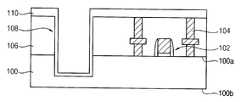
도 1을 참조하면, 회로 패턴(102)들이 구비된 기판(100)을 마련한다. 기판(100)은 제1 면(100a) 및 제1 면(100a)에 반대하는 제2 면(100b)을 갖는다. 기판(100)은 반도체 물질로 이루어진 기판일 수 있으며, 일 예로, 단결정 실리콘 기판일 수 있다.Referring to FIG. 1, a
회로 패턴(102)들은 기판(100)의 제1 면(100a) 상에 형성되며, 회로 패턴(102)들은 트랜지스터, 다이오드 등을 포함할 수 있다. 또한 회로 패턴(102)들은 다수개의 메모리 소자들을 포함할 수도 있다. 상기 메모리 소자의 예로써 휘발성 반도체 메모리 소자와 비휘발성 반도체 메모리 소자를 들 수 있다. 상기 휘발성 반도체 메모리 소자의 예로는 DRAM, SRAM 등이 있으며, 상기 비휘발성 반도체 메모리 소자의 예로는 EPROM, EEPROM, Flash EEPROM 등이 있다.The
상기 기판(100) 상에는 회로 패턴(102)들을 덮는 층간 절연막(106)이 구비된다. 회로 패턴(102)들은 폴리실리콘 혹은 금속을 포함하는 콘택 플러그(104)들에 의해 전기적으로 연결될 수 있다.An interlayer insulating
층간 절연막(106) 및 기판(100) 내에는, 층간 절연막(106)을 관통하여 기판(100) 내부까지 연장되는 개구부(108)가 구비될 수 있다. 하나의 반도체 칩을 이루는 기판(100)에는 복수개의 개구부(108)가 구비될 수 있다.In the interlayer insulating
개구부(108) 내부의 측벽 및 저면과 층간 절연막(106) 상부면 프로파일을 따라 절연막 패턴(114a)이 구비된다. 절연막 패턴(114a)은 기판(100)과 개구부(108)를 매립하는 도전 물질 사이를 절연시키는 역할을 한다.An insulating
개구부(108)의 측벽 상에 형성된 절연막 패턴(114a) 부분은 내부에 에어 갭(air gap, 112a)을 포함할 수 있다. 에어 갭(112a)이 형성됨으로써 개구부(108)를 매립하는 도전 물질과 기판(100) 사이의 기생 커패시턴스를 현격하게 감소시킬 수 있다.A portion of the insulating
개구부(108)의 측벽 및 저면 상에 형성된 절연막 패턴(114a) 상에는 배리어 금속막 패턴(120)이 구비된다. 배리어 금속막 패턴(120)은 Ta, TaN, Ti, TiN, Ru, Co, Ni, NiB, WN 등의 물질을 포함할 수 있다. 이들은 단독으로 사용되거나 또는 2 이상을 적층하여 사용할 수도 있다.The barrier
배리어 금속막 패턴(120) 상에는 개구부(108)의 나머지 부분을 채우는 관통 전극(125)이 구비된다. 관통 전극(125)은 저저항을 갖는 금속을 포함할 수 있다. 예시적인 실시예들에 있어서, 관통 전극(125)은 구리(Cu) 또는 텅스텐(W)을 포함할 수 있다.The through
배리어 금속막 패턴(120), 관통 전극(125) 및 절연막 패턴(114a) 상에 버퍼막(130)이 구비된다. 버퍼막(130)은 관통 전극(125)의 도전 물질이 확산되는 것을 방지하는 역할을 한다. 버퍼막(130)은 실리콘 질화물, 실리콘 탄질화물, SiCON 등을 포함할 수 있다. 이들은 단독으로 사용되거나 또는 2 이상을 적층하여 사용할 수도 있다.The
버퍼막(130) 상에는 제1 금속간 절연막(IMD, Inter Metal Dielectric, 135)이 구비된다. 제1 금속간 절연막(135)은 저유전율을 갖는 물질을 포함할 수 있으며, 예를 들어 실리콘 산화물, 탄소 도핑된 실리콘 산화물 등을 포함할 수 있다.The first intermetal dielectric (IMD, Inter Metal Dielectric) 135 is provided on the
제1 금속간 절연막(135) 및 버퍼막(130)을 관통하여 관통 전극(125)과 전기적으로 연결되며, 제1 금속간 절연막(135), 버퍼막(130) 및 절연막 패턴(114a)을 관통하여 콘택 플러그(104)들과 전기적으로 연결되는 제1 금속 배선(145)들이 구비된다.The first intermetallic insulating
제1 금속간 절연막(135) 및 제1 금속 배선(145) 상에, 제2 금속간 절연막(150) 및 제1 금속 배선(145)과 전기적으로 연결되는 제2 금속 배선(155)이 구비된다. 도시하지는 않았으나, 상기 제2 금속간 절연막(150) 및 제2 금속 배선(155) 상에 제3 금속간 절연막 및 제3 배선을 더 구비할 수도 있다.On the first intermetallic insulating
도 2 내지 도 12는 제1 실시예에 따른 반도체 소자 제조 방법을 설명하기 위한 단면도들이다.2 to 12 are cross-sectional views illustrating a method of manufacturing a semiconductor device in accordance with a first embodiment.
도 2를 참조하면, 기판(100)의 제1 면(100a) 상에 회로 패턴(102)을 형성하고, 회로 패턴(102)들을 덮는 층간 절연막(106)을 기판(100) 상에 형성한다.Referring to FIG. 2, a
기판(100)은 실리콘 기판, 게르마늄 기판, 실리콘-게르마늄 기판, 실리콘-온-인슐레이터(Silicon-On-Insulator: SOI) 기판, 게르마늄-온-인슐레이터(Germanium-On-Insulator: GOI) 기판 등 반도체 기판을 포함할 수 있다. 한편, 도시하지는 않았으나, 기판(100)은 p형 혹은 n형 불순물을 포함하는 웰(well)을 더 포함할 수도 있다.The
회로 패턴(102)은 CMOS 트랜지터, 다이오드 등을 포함할 수 있다.The
층간 절연막(106)은 실리콘 산화물 등을 사용하여 화학 기상 증착(Chemical Vapor Deposition : CVD) 공정 등을 통해 형성할 수 있다.The interlayer insulating
도 2를 계속하여 참조하면, 층간 절연막(106)을 관통하여 회로 패턴(102)의 일부와 전기적으로 연결되는 콘택 플러그(104)를 형성한다.With continued reference to FIG. 2, a
구체적으로, 층간 절연막(106)의 일부를 식각하여 회로 패턴(102)의 일부를 노출시키는 콘택 홀(도시되지 않음)을 형성한다. 상기 콘택 홀 내부를 채우는 금속막을 형성하고 층간 절연막(106)의 상면이 노출될 때까지 상기 금속막을 연마하여 콘택 플러그(104)을 형성한다.Specifically, a portion of the interlayer insulating
예시적인 실시예들에 있어서, 상기 금속막은 구리(Cu) 혹은 텅스텐(W)을 사용하여 형성할 수 있다.In example embodiments, the metal layer may be formed using copper (Cu) or tungsten (W).
본 발명의 예시적인 실시예들에 따르면, 전공정(front-end-of-line, FEOL)이라 불리는 웨이퍼 공정을 수행하여 기판(100) 상에 회로 패턴(102)들을 형성한다. 후술하는 바와 같이, 기판(100) 상에 회로 패턴들(102)을 형성한 후, 후공정(back-end-of-line, BEOL)이라 불리는 배선 공정을 수행하기 전에 관통 전극(도 8 참조, 125)을 형성한다.In accordance with exemplary embodiments of the present invention, a wafer process called front-end-of-line (FEOL) is performed to form
도 3을 참조하면, 층간 절연막(106)을 관통하고 기판(100) 내부까지 연장하는 개구부(108)를 형성한다. 개구부(108)의 측벽은 층간 절연막(106) 및 기판(100)에 의해 정의되고, 개구부(108)의 저면은 기판(100)에 의해 정의된다.Referring to FIG. 3, an
구체적으로, 층간 절연막(106) 상에 포토 레지스트 패턴(도시되지 않음)을 형성하고, 상기 포토 레지스트 패턴을 식각 마스크로 사용하여 층간 절연막(106)을 식각하고, 계속하여 기판(100)의 일부를 건식 식각한다.Specifically, a photoresist pattern (not shown) is formed on the
상기 포토레지스트 패턴은 애싱 및/또는 스트립 공정을 통해 제거될 수 있다.The photoresist pattern may be removed through an ashing and / or strip process.
도 4를 참조하면, 층간 절연막(106)의 상면과 개구부(108) 내부의 측벽 및 저면의 프로파일을 따라 제1 절연막(110)을 형성한다.Referring to FIG. 4, the first insulating
제1 절연막(110)은 실리콘 산화물 또는 탄소 도핑된 실리콘 산화물을 이용하여 형성할 수 있다. 예시적인 실시예들에 있어서, 제1 절연막(110)은 플라즈마 산화 공정을 통해 형성하거나 CVD 공정등을 통해 형성할 수 있으며, 스텝 커버리지 특성이 우수한 TEOS막, 오존 TEOS 막 등을 이용하여 형성할 수 있다. 제1 절연막(110)은 기판(100)과 개구부(108) 내부의 도전 물질을 절연시키는 역할을 수행할 수 있다.The first insulating
도 5를 참조하면, 개구부(108)의 측벽 상에 형성된 제1 절연막(110) 부분 상에 희생막 패턴(112)을 형성한다.Referring to FIG. 5, a
희생막 패턴(112)은 제1 절연막(110) 상에 희생막(도시되지 않음)을 형성하고 상기 희생막을 이방성 식각함으로써 형성될 수 있다. 상기 희생막은 탄화수소(hydrocarbon, CxHy) 계열의 물질을 사용하여 형성할 수 있다. 예시적인 실시예들에 있어서, 상기 탄화수소 계열 물질은 방향족 혹은 비방향족의 고리형 또는 다리형 탄화수소 물질을 포함할 수 있다. 예를 들면, 상기 희생막은 테르핀(terpine) 혹은 노르보넨(norbornene) 계열의 물질을 사용하여 형성할 수 있다.The
도 6을 참조하면, 제1 절연막(110) 및 희생막 패턴(112) 상에 제2 절연막을 증착하여 예비 절연막 패턴(114)을 형성한다.Referring to FIG. 6, a second insulating layer is deposited on the first insulating
예시적인 실시예들에 있어서, 상기 제2 절연막은 실리콘 산화물 또는 탄소 도핑된 실리콘 산화물을 이용하여 형성할 수 있으며, 도 5에 도시된 제1 절연막(110)과 동일한 물질을 사용하여 형성될 수도 있다. 제1 절연막(110) 상에 형성되는 상기 제2 절연막 부분은 제1 절연막(110)과 병합되어 형성될 수 있다. 따라서 제1 절연막(110) 및 상기 제2 절연막이 병합되며, 개구부(108)의 측벽 상에서는 내부에 희생막 패턴(112)을 포함하는 예비 절연막 패턴(114)을 형성할 수 있다.In example embodiments, the second insulating layer may be formed using silicon oxide or carbon doped silicon oxide, or may be formed using the same material as the first insulating
도 7을 참조하면, 희생막 패턴(112)을 제거함으로써 에어 갭(112a)을 포함하는 절연막 패턴(114a)을 형성한다.Referring to FIG. 7, the insulating
희생막 패턴(112)은 예비 절연막 패턴(114) 상에 열처리를 수반한 광 조사 처리를 수행하여 제거될 수 있다. 예시적인 실시예들에 있어서, 상기 광 조사 처리는 200nm 내지 600nm 범위의 파장을 갖는 자외선(ultra violet, UV) 광원을 사용하여 수행될 수 있다. 자외선 광에 의해 희생막 패턴(112)에 포함된 탄화수소 계열의 물질들은 기화되거나 분자들의 결합이 깨어져 제거될 수 있다. 상기 자외선 광의 파장이 200nm 미만일 경우 예비 절연막 패턴(114)이 손상될 수 있고, 상기 자외선 광의 파장이 600nm를 초과하는 경우 희생막 패턴(112)이 용이하게 제거되지 않을 수 있다.The
일 실시예에 따르면, 상기 광 조사 처리는 300 내지 500℃의 온도 조건에서 수행될 수 있다. 상기 광 조사 처리가 300℃ 미만의 온도에서 수행될 경우 희생막 패턴(112)이 용이하게 제거되기 곤란하고, 500℃를 초과하는 온도에서 수행될 경우는 예비 절연막 패턴(114)이 손상될 수 있다.According to one embodiment, the light irradiation treatment may be performed at a temperature condition of 300 to 500 ℃. When the light irradiation treatment is performed at a temperature below 300 ° C., the
이와는 달리, 희생막 패턴(112)은 전자빔(electron beam) 조사 공정을 수행하여 제거될 수도 있다.Alternatively, the
도 7에 도시된 바와 같이, 희생막 패턴(112)이 제거된 공간에는 에어 갭(112a)이 정의되며, 따라서 개구부(108)의 측벽 상에 에어갭(112a)을 포함하는 절연막 패턴(114a)이 형성된다.As shown in FIG. 7, the
에어 갭(112a)이 절연막 패턴(114a) 내부에 형성됨으로써, 후속 공정에 의해 형성되는 관통 전극(125) 및 기판(100) 사이의 기생 커패시턴스를 현격히 감소시킬 수 있다.Since the
도 8을 참조하면, 절연막 패턴(114a)이 형성된 개구부(108)를 매립하는 배리어 금속막 패턴(120) 및 관통 전극(125)을 형성한다.Referring to FIG. 8, the barrier
구체적으로, 절연막 패턴(114a) 상에 배리어 금속막을 형성한다. 상기 배리어 금속막은 Ta, TaN, Ru, Co, Mn, TiN, Ti/TiN, WN, Ni, NB 등의 물질을 사용하여 형성할 수 있다. 이들은 단독 혹은 2이상이 적층되어 형성될 수도 있다.Specifically, a barrier metal film is formed on the insulating
상기 배리어 금속막 상에 시드막(도시되지 않음)을 형성한다. 상기 시드막은 후속 공정에서 도전막을 형성하기 위한 도금 공정에서 전극으로 사용될 수 있다. 상기 시드막은 구리(Cu), 알루미늄(Al), 티타늄(Ti), 탄탈륨(Ta), 텅스텐(W) 등의 금속 물질을 사용하여 물리기상증착 공정 등을 통해 형성할 수 있다. 예를 들면, 상기 시드막은 저저항을 갖는 구리를 사용하여 형성할 수 있다.A seed film (not shown) is formed on the barrier metal film. The seed film may be used as an electrode in a plating process for forming a conductive film in a subsequent process. The seed layer may be formed through a physical vapor deposition process using metal materials such as copper (Cu), aluminum (Al), titanium (Ti), tantalum (Ta), and tungsten (W). For example, the seed layer may be formed using copper having low resistance.
상기 시드막 상에 개구부(108) 내부를 채우는 도전막을 형성한다. 상기 도전막은 상기 시드막과 같이 금속 물질을 사용하여 형성할 수 있으며,예를 들면, 저저항의 구리를 사용하여 형성할 수 있다.A conductive film filling the inside of the
상기 도전막은 전해 도금법, 무전해 도금법, 전자 융합법(electrografting) 등을 통해 형성할 수 있다. 상기 도전막 형성 이후, 열처리(annealing) 공정을 더 수행할 수도 있다.The conductive film may be formed by an electroplating method, an electroless plating method, an electron fusion method, or the like. After the conductive film is formed, annealing may be further performed.
이어서, 상기 도전막 및 배리어 금속막을 화학 기계적 연마(chemical mechanical polishing, CMP) 공정을 통해 절연막 패턴(114a)의 상면이 노출될 때까지 평탄화하여 배리어 금속막 패턴(120) 및 관통 전극(125)을 형성한다.Subsequently, the conductive film and the barrier metal film are planarized through a chemical mechanical polishing (CMP) process until the top surface of the insulating
이와는 다르게, 도시되지는 않았으나, 개구부(108)를 매립하는 도전막을 절연막 패턴(114a) 상에 화학기상증착, 물리기상증착 공정등을 통해 형성한 후, 이를 CMP 공정등을 통해 평탄화하여 관통 전극(125)을 형성할 수도 있다.Unlike this, although not shown, a conductive film filling the
도 9를 참조하면, 절연막 패턴(114a) 상에 배리어 금속막 패턴(120) 및 관통 전극(125)을 덮는 버퍼막(130)을 형성한다.Referring to FIG. 9, a
버퍼막(130)은 실리콘 질화물, 실리콘 탄질화물, SiCON 등의 물질을 사용하여 형성할 수 있다. 이들은 단독 혹은 2 이상을 적층하여 형성할 수 있다. 버퍼막(130)을 형성함으로써, 관통 전극(125)에 포함되는 금속 물질의 확산을 억제할 수 있다.The
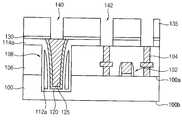
도 10을 참조하면, 각각 관통 전극(125) 및 콘택 플러그(104) 상면을 노출시키는 제1 트렌치(140) 및 제2 트렌치(142)를 형성한다.Referring to FIG. 10, first and
구체적으로, 버퍼막(130) 상에 제1 금속간 절연막(Inter Metal Dielectric, IMD, 135)을 형성한다. 제1 금속간 절연막(135) 및 버퍼막(130)을 부분적으로 식각함으로써 관통 전극(125)의 상면을 일부 노출시키는 제1 트렌치(140)를 형성한다. 한편, 계속하여 콘택 플러그(104)의 상면이 노출될 때까지 절연막 패턴(114a)을 부분적으로 식각하여 제2 트렌치(142)를 형성한다. 예시적인 실시예들에 있어서, 제1 및 제2 트렌치(140, 142)들은 습식 식각 공정을 통해 형성될 수 있다.In detail, a first intermetal dielectric (IMD) 135 is formed on the
도 11을 참조하면, 제1 및 제2 트렌치들(140, 142)을 채우며 관통 전극(125) 및 콘택 플러그(104)와 전기적으로 연결되는 제1 금속 배선(145)을 형성한다.Referring to FIG. 11, a
제1 금속 배선(145)은 제1 및 제2 트렌치들(140, 142)를 채우는 도전막을 제1 금속간 절연막(135) 상에 형성한 후 제1 금속간 절연막(135) 상면이 노출될 때까지 평탄화하여 형성할 수 있다.When the upper surface of the first intermetallic insulating
도 12를 참조하면, 제1 금속간 절연막(135) 및 제1 금속 배선(145) 상에 제2 금속간 절연막(150) 및 제2 금속 배선(155)을 형성한다.12, a second intermetallic insulating
구체적으로, 제1 금속간 절연막(135) 및 제1 금속 배선(145) 상에 제2 금속간 절연막(150)을 형성하고 이를 일부 식각하여 제1 금속 배선(145)의 상면 일부를 노출시키는 제3 트렌치(도시되지 않음)을 형성한다. 상기 제3 개구부 내에 도전 물질을 채워 제1 금속 배선(145)과 전기적으로 연결되는 제2 금속 배선을 형성한다.Specifically, the second intermetallic insulating
도시하지는 않았지만, 상기와 동일한 공정을 수행하여 제3 금속간 절연막 및 제3 금속 배선을 더 형성할 수도 있다.Although not shown, the same process as above may be performed to further form the third intermetallic insulating film and the third metal wiring.
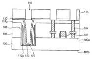
도 13 내지 도 17은 다른 실시예들에 따른 반도체 소자의 제조 방법을 설명하기 위한 단면도들이다. 도 2 내지 도 12를 참조로 설명한 제1 실시예와는 콘택 플러그(104)가 형성되는 단계 및 높이에 있어서 차이가 있고, 나머지는 실질적으로 동일하므로 중복되는 부분에 대해서는 자세한 설명을 생략한다. 또한 동일 혹은 유사한 구성요소에 대해서는 동일한 참조번호를 사용한다.13 to 17 are cross-sectional views illustrating a method of manufacturing a semiconductor device in accordance with other embodiments. The first embodiment described with reference to FIGS. 2 to 12 has a difference in steps and heights at which the
도 13을 참조하면, 기판(100)의 제1 면(100a) 상에 회로 패턴(102)을 형성하고, 회로 패턴(102)들을 덮는 층간 절연막(106)을 기판(100) 상에 형성한다.Referring to FIG. 13, a
이후, 층간 절연막(106)을 관통하고 기판(100) 내부까지 연장하는 개구부(108)를 형성한다.Thereafter, an
도 14를 참조하면, 도 4 내지 도 9를 참조로 설명한 공정들과 실질적으로 동일한 공정들을 수행하여, 에어 갭(114a)을 포함하는 절연막 패턴(114a)과 개구부(108)를 매립하는 배리어 금속막 패턴(120) 및 관통 전극(125)을 형성한다. 이후, 절연막 패턴(114a), 배리어 금속막 패턴(120) 및 관통 전극(125)을 덮는 버퍼막(130)을 형성한다.Referring to FIG. 14, the barrier metal film filling the
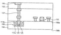
도 15를 참조하면, 버퍼막(130), 절연막 패턴(114a) 및 층간 절연막(106)을 관통하고 회로 패턴(102) 일부와 전기적으로 연결되는 콘택 플러그(104)를 형성한다.Referring to FIG. 15, a
구체적으로, 사진 식각 공정을 통해 버퍼막(130), 절연막 패턴(114a) 및 층간 절연막(106)을 순차적으로 식각하여, 버퍼막(130), 절연막 패턴(114a) 및 층간 절연막(106)을 관통하며 회로 패턴(102) 일부의 상면을 노출시키는 콘택홀(도시되지 않음)을 형성한다. 상기 콘택홀을 매립하는 도전막을 버퍼막(130) 상에 형성하고 상기 도전막 상부를 평탄화하여 콘택 플러그(104)를 형성할 수 있다. 예시적인 실시예들에 있어서, 상기 도전막은 구리 또는 텅스텐을 포함할 수 있다.In detail, the
일 실시예에 있어서, 상기 도전막을 형성하기 전에 상기 콘택홀의 측벽 및 저면 상에 배리어 금속막을 형성할 수도 있다.In example embodiments, a barrier metal layer may be formed on sidewalls and bottom surfaces of the contact hole before the conductive layer is formed.
콘택 플러그(104)를 형성함으로써 FEOL 공정이 완료되고 금속 배선들을 형성하는 BEOL 공정을 수행한다.By forming the
도 16을 참조하면, 관통전극(125) 및 콘택 플러그 상면을 노출시키는 트렌치(140)들을 형성한다.Referring to FIG. 16,
구체적으로, 버퍼막(130) 상에 콘택 플러그(104)를 덮는 제1 금속간 절연막(135)을 형성하고, 제1 금속간 절연막(135) 및 버퍼막(130)의 일부를 식각함으로써 트렌치(140)들을 형성할 수 있다. 이 때, 콘택 플러그(104)의 상부의 일부가 함께 제거될 수도 있으며, 이에 따라 관통 전극(125) 및 콘택 플러그(104)의 상면은 절연막 패턴(114a)의 상면과 동일한 높이를 갖도록 형성될 수 있다.In detail, a trench may be formed by forming a first intermetallic insulating
예시적인 실시예들에 있어서, 트렌치(140)들의 형성을 위한 식각 공정은 건식 식각 공정을 통해 수행될 수 있다.In example embodiments, an etching process for forming the
도 17을 참조하면, 트렌치(140)들을 채우며 관통 전극(125) 및 콘택 플러그(104)와 전기적으로 연결되는 제1 금속배선(145)을 형성한다.Referring to FIG. 17, the
이후, 도시하지는 않았으나, 도 12를 참조로 설명한 공정들과 동일한 공정들을 수행하여 제1 금속간 절연막(135) 및 제1 금속 배선(145) 상에 제2 금속간 절연막 및 제2 금속 배선을 더 형성할 수도 있다. 또한 상기와 동일한 공정을 수행하여, 제3 금속간 절연막 및 제3 금속 배선을 더 형성할 수도 있다.
Subsequently, although not shown, the second intermetallic insulating film and the second metal wiring are further formed on the first intermetallic insulating
실시예 2Example 2
도 18은 제2 실시예에 따른 반도체 소자를 나타내기 위한 단면도이다.18 is a cross-sectional view illustrating a semiconductor device according to a second embodiment.
도 1을 참조로 설명한 제1 실시예에 따른 반도체 소자와는 달리, 제2 실시예의 반도체 소자에 따르면 개구부(108)는 기판(100)의 제1 면(100a)에서 기판 내부로 연장한다.Unlike the semiconductor device according to the first embodiment described with reference to FIG. 1, according to the semiconductor device of the second embodiment, the
개구부(108) 내부의 측벽 및 저면 상에는 에어 갭(112a)을 포함하는 절연막 패턴(114a)이 구비되고, 절연막 패턴(114a) 상에는 배리어 금속막(120)이 구비되며, 개구부(108)의 나머지 부분을 채우는 관통 전극(125)이 구비된다.An insulating
기판(100) 상에는 회로 패턴(102)들이 구비되고, 회로 패턴(102)들을 덮는 층간 절연막(106)이 구비된다. 층간 절연막(127)은 관통 전극(125)과 전기적으로 연결되는 하부 배선(127)을 포함한다.
층간 절연막(106) 및 하부 배선(127) 상에는 제1 금속간 절연막(135) 및 제1 금속 배선(145)이 구비된다.The first intermetallic insulating
도시되지는 않았으나, 제1 금속간 절연막(135) 및 제1 금속 배선(145) 상에는 복수의 금속간 절연막들 및 금속 배선들이 더 구비될 수도 있다.Although not shown, a plurality of intermetallic insulating layers and metal lines may be further provided on the first intermetallic insulating
도 19 내지 도 21은 제2 실시예에 따른 반도체 소자의 제조 방법을 설명하기 위한 단면도들이다.19 to 21 are cross-sectional views illustrating a method of manufacturing a semiconductor device in accordance with a second embodiment.
도 19를 참조하면 기판(100)의 제1 면(100a)으로부터 기판(100) 내부로 연장하는 개구부(108)를 형성하고, 기판(100)의 제1 면(100a), 개구부(108)의 측벽 및 저면의 프로파일을 따라 절연막 패턴(114a)을 형성한다. 개구부(108)의 측벽 상에 형성된 절연막 패턴(114a) 부분은 내부에 에어 갭(112a)을 포함할 수 있다.Referring to FIG. 19, an
절연막 패턴(114a) 및 에어 갭(112a)의 형성 공정은 도 4 내지 도 7을 참조로 설명한 공정들과 실질적으로 유사하므로 자세한 설명은 생략한다.Since the process of forming the insulating
도 20을 참조하면, 도 8을 참조로 설명한 공정들과 실질적으로 유사한 공정을 수행함으로써, 개구부(108) 내부를 채우는 배리어 금속막(120) 및 관통 전극(125)을 형성한다.Referring to FIG. 20, a
도 21을 참조하면, 관통 전극(125)과 전기적으로 연결되는 하부 배선(127)을 형성하고, 하부 배선(127)과 연결되는 제1 금속 배선(145)을 형성한다.Referring to FIG. 21, a
구체적으로, 절연막 패턴(114a), 배리어 금속막(120) 및 관통 전극(125)의 상부를 연마하여 기판(100)의 제1 면(100a)을 노출시킨다.In detail, the upper surface of the insulating
기판(100)의 제1 면(100a) 상에 회로 패턴(102)들을 형성하고 회로 패턴(102)들을 덮는 층간 절연막(106)을 형성한다. 층간 절연막(106) 내부에 관통 전극(108)과 전기적으로 연결되는 하부 배선(127)을 형성한다.
층간 절연막(106) 및 하부 배선(127) 상에 제1 금속간 절연막(135)을 형성하고 제1 금속간 절연막(135) 내부에 하부 배선(127)과 연결되는 제1 금속 배선(145)을 형성한다.The first intermetallic insulating
도시되지는 않았지만, 제1 금속간 절연막(135) 및 제1 금속 배선(145) 상에 복수의 금속간 절연막 및 금속 배선들이 더 형성될 수도 있다.Although not shown, a plurality of intermetallic insulating films and metal wires may be further formed on the first intermetallic insulating
도 22는 예시적인 실시예들에 따른 도 1에 도시된 반도체 소자를 포함하는 적층형 반도체 소자를 나타내는 단면도이다.FIG. 22 is a cross-sectional view illustrating a stacked semiconductor device including the semiconductor device illustrated in FIG. 1 according to example embodiments.
도 22를 참조하면, 상기 적층형 반도체 소자는 제1 반도체 칩(A), 제2 반도체 칩(B) 및 접촉 패턴들(175, 240)을 포함한다.Referring to FIG. 22, the stacked semiconductor device includes a first semiconductor chip A, a second semiconductor chip B, and
상기 제1 반도체 칩(A)은 제1 회로 패턴(102)를 포함하며, 제1 회로 패턴(102)은 메모리 소자, 로직 소자 혹은 이미지 소자등을 포함할 수 있다. 제1 반도체 칩(A)은 제1 기판(100)에 형성되며, 배리어 금속막 패턴(120) 및 관통 전극(125)의 저면이 제1 기판(100)의 제2 면(100b)에 노출되어 있는 것을 제외하고는 도 1에 도시된 상기 반도체 소자와 실질적으로 동일한 구성을 가질 수 있다. 따라서, 도 1에 도시된 상기 반도체 소자와 차이점에 대해서만 설명하고자 한다.The first semiconductor chip A may include a
예시적인 실시예들에 있어서, 도 1에 도시된 반도체 소자의 기판(100)의 제2 면(100b)을 관통 전극(125)의 저면이 노출될 때까지 연마함으로써, 배리어 금속막 패턴(120) 및 관통 전극(125)의 저면을 노출시킬 수 있다.In example embodiments, the barrier
한편, 이에 더하여, 제1 반도체 칩(A)의 최상부에 위치한 제3 금속 배선(165) 및 제3 금속간 절연막(160) 상에는 제1 보호막(170)이 구비될 수 있다. 제1 보호막(170)은 절연 물질을 포함하며, 예를 들면, 폴리이미드를 포함할 수 있다. 제1 보호막(170)은 패드 전극으로 제공되는 최상부의 제3 금속 배선(하기에서는 이를 제1 패드 전극으로 지칭한다, 165)과 전기적으로 연결되는 제1 접촉 패턴(175)를 포함할 수 있다.In addition, the
제1 접촉 패턴(175)은 인쇄 회로 기판과 접촉할 수 있다. 이와는 달리, 도시하지는 않았지만, 와이어 본딩에 의해 제1 패드 전극(165)이 리드 프레임과 전기적으로 연결될 수도 있다.The
제2 반도체 칩(B)은 제2 기판(200), 제2 기판(200) 상에 구비되는 제2 회로 패턴들(202), 배선들(220), 층간 절연막들(210) 및 관통 전극(125)을 통해 신호가 인가되는 제2 패드 전극(230)을 포함한다.The second semiconductor chip B may include the second substrate 200, the second circuit patterns 202, the
제2 반도체 칩(B)에 포함되는 반도체 소자는 제1 반도체 칩(A)에 포함된 것과 동일한 반도체 소자일 수도 있고, 상이한 반도체 소자일 수도 있다.The semiconductor element included in the second semiconductor chip B may be the same semiconductor element as that included in the first semiconductor chip A, or may be a different semiconductor element.
도 22에 도시된 바와 같이, 제2 반도체 칩(B)의 최상부에 형성된 층간 절연막(210)에는 배선들(220)과 연결되는 제2 패드 전극(230)이 구비된다. 제2 패드 전극(230)은 제1 기판(100)의 관통 전극(125)의 저면과 접합되어 전기적으로 연결되어 있다.As illustrated in FIG. 22, a
최상부의 층간 절연막(210) 및 제2 패드 전극(230) 상에는 제2 보호막(235)이 구비된다. 제2 보호막(235)은 폴리이미드 물질을 포함할 수 있다.The
제2 보호막(235)은 관통 전극(125) 및 제2 패드 전극(230)을 전기적으로 연결하는 제2 접촉 패턴(240)을 포함한다. 제2 접촉 패턴(240)으로 사용될 수 있는 물질의 예로는 은(Ag) 솔더 페이스트 등을 들 수 있다.The
도 22에 도시된 실시예에 따른 적층형 반도체 소자는 절연막 패턴(114a) 내에 형성된 에어 갭(112a)에 의해 기생 커패시턴스가 감소되어 빠른 신호 전달 속도를 갖는다.In the stacked semiconductor device according to the exemplary embodiment illustrated in FIG. 22, the parasitic capacitance is reduced by the
한편, 도시하지는 않았지만, 관통 전극(125)을 포함하는 동일한 제1 반도체 칩(A)이 3개 이상 수직으로 적층될 수도 있다. 이 때, 각 반도체 칩 내의 관통 전극(125)의 저면은 다른 칩의 최상부 패드 전극과 솔더, 범프 등을 통해 전기적으로 접촉되는 형상을 가질 수 있다.Although not shown, three or more identical first semiconductor chips A including the through
도 23 내지 도 24는 도 22에 도시된 적층형 반도체 소자의 제조 방법을 설명하기 위한 부분 단면도이다.23 to 24 are partial cross-sectional views for describing a method of manufacturing the stacked semiconductor device illustrated in FIG. 22.
도 23을 참조하면, 도 2 내지 도 12를 참조로 설명한 공정들과 동일한 공정을 수행하여, 관통 전극(125) 측부에 에어 갭(112a)을 구비하고 관통전극과 전기적으로 연결되는 금속배선들(145, 155, 165)을 포함하는 반도체 소자를 제조한다.Referring to FIG. 23, metal wires having an
최상부의 제3 금속간 절연막(160) 및 제3 금속 배선(165) 상에 폴리이미드 물질들을 사용하여 제1 보호막(170)을 형성한다.The
제1 보호막(170)의 일부를 제거하여 제3 금속 배선(165)을 노출시키는 개구부를 형성하고, 제1 보호막(170) 상에 제3 금속 배선(165)과 접촉하는 제1 접촉 패턴(175)을 형성한다.A portion of the
이후, 기판(100)의 제2 면(100b)을 연마하여 관통 전극(125) 및 배리어 금속막(120)의 하면을 노출시킴으로써 제1 반도체 칩(A)을 형성한다.Thereafter, the
도 24를 참조하면, 제1 반도체 칩(A)을 관통 전극(125)을 이용하여 제2 반도체 칩(B)과 적층시킨다.Referring to FIG. 24, the first semiconductor chip A is stacked with the second semiconductor chip B using the through
관통 전극(125)을 제2 반도체 칩(B)의 제2 접촉 패턴(240)에 부착시킴으로서 제1 반도체 칩(A)을 제2 반도체 칩(B) 상에 적층시킬 수 있다.The first semiconductor chip A may be stacked on the second semiconductor chip B by attaching the through
제2 반도체 칩(B)은 제1 반도체 칩(A)과 동일한 반도체 소자일 수도 있고, 상이한 반도체 소자일 수도 있다.The second semiconductor chip B may be the same semiconductor element as the first semiconductor chip A or may be a different semiconductor element.
도시되지는 않았지만 범프를 제2 접촉 패턴(240)에 부착시켜 상기 범프를 매개로 제1 반도체 칩(A)을 제2 반도체 칩(B) 상에 적층시킬 수도 있다.Although not shown, a bump may be attached to the
한편, 제1 반도체 칩(A) 상에도 제1 접촉 패턴(175)을 매개로 동일한 혹은 다른 반도체 소자를 적층시킬 수도 있다.Meanwhile, the same or different semiconductor elements may be stacked on the first semiconductor chip A via the
본 발명의 실시예들에 따르면, 기판 내부로 연장하는 개구부 내부에 에어 갭을 포함하는 절연막 패턴을 형성하고, 상기 개구부 내부를 채우는 관통 전극을 형성한다. 상기 에어 갭을 형성함으로써 기존의 저유전 물질을 사용하여 상기 절연막 패턴을 형성하는 것보다 상기 관통 전극 및 기판 사이의 기생 커패시턴스를 현격하게 감소시킬 수 있다. 이에 따라 반도체 소자의 신호 전달 속도를 향상시킬 수 있으며, 반도체 소자의 안정적이고 신뢰성 있는 동작 특성을 확보할 수 있다.According to embodiments of the present invention, an insulating film pattern including an air gap is formed in an opening extending into the substrate, and a through electrode filling the inside of the opening is formed. By forming the air gap, the parasitic capacitance between the through electrode and the substrate may be significantly reduced, rather than using the existing low dielectric material to form the insulating layer pattern. Accordingly, the signal transmission speed of the semiconductor device can be improved, and stable and reliable operation characteristics of the semiconductor device can be secured.
상술한 바와 같이 본 발명의 예시적인 실시예들을 참조하여 설명하였지만 해당 기술 분야에서 통상의 지식을 가진 자라면 하기의 특허 청구 범위에 기재된 본 발명의 사상 및 영역으로부터 벗어나지 않는 범위 내에서 본 발명을 다양하게 수정 및 변경시킬 수 있음을 이해할 수 있을 것이다.Although described with reference to exemplary embodiments of the present invention as described above, those skilled in the art to which the present invention pertains without departing from the spirit and scope of the present invention as set forth in the claims below It will be understood that modifications and changes can be made.
100 : 기판102 : 회로 패턴
104 : 콘택 플러그106 : 층간 절연막
108 : 개구부110 : 제1 절연막
112 : 희생막 패턴114 : 예비 절연막 패턴
112a : 에어 갭114a : 절연막 패턴
120 : 배리어 금속막 패턴125 : 관통전극
127 : 하부 배선130 : 버퍼막
135 : 제1 금속간 절연막140 : 제1 트렌치
142 : 제2 트렌치145 : 제1 금속 배선
150 : 제2 금속간 절연막155 : 제2 금속 배선
160 : 제3 금속간 절연막165 : 제3 금속 배선
170 : 제1 보호막175 : 제1 접촉패턴
200 : 제2 기판202 : 제2 회로 패턴
220 : 배선210 : 층간절연막
230 : 제2 패드 전극235 : 제2 보호막
240 : 제2 접촉 패턴100: substrate 102: circuit pattern
104: contact plug 106: interlayer insulating film
108: opening 110: first insulating film
112: sacrificial film pattern 114: preliminary insulating film pattern
112a:
120: barrier metal film pattern 125: through electrode
127: lower wiring 130: buffer film
135: first intermetallic insulating film 140: first trench
142: second trench 145: first metal wiring
150: second intermetallic insulating film 155: second metal wiring
160: third intermetallic insulating film 165: third metal wiring
170: first protective film 175: first contact pattern
200: second substrate 202: second circuit pattern
220: wiring 210: interlayer insulating film
230: second pad electrode 235: second protective film
240: second contact pattern
Claims (10)
Translated fromKorean상기 개구부 내부의 측벽 상에 형성되고, 에어 갭을 내부에 갖는 절연막 패턴;
상기 개구부를 매립하는 관통 전극; 및
상기 관통 전극과 전기적으로 연결되는 금속 배선을 포함하는 반도체 소자.A substrate having a first surface and a second surface opposite the first surface, the substrate having an opening extending inwardly from the first surface;
An insulating film pattern formed on a sidewall of the opening and having an air gap therein;
A through electrode filling the opening; And
And a metal wire electrically connected to the through electrode.
상기 제1 절연막 및 상기 제2 절연막 사이에 상기 에어 갭이 정의되는 것을 특징으로 하는 반도체 소자.The method of claim 1, wherein the insulating layer pattern includes a first insulating layer formed on a sidewall of the opening and a second insulating layer formed on the first insulating layer.
The air gap is defined between the first insulating film and the second insulating film.
상기 개구부는 상기 층간 절연막의 상면으로부터 상기 기판 내부로 연장하는 것을 특징으로 하는 반도체 소자.The semiconductor device of claim 1, further comprising an interlayer insulating layer covering the circuit pattern and the circuit pattern on the first surface of the substrate,
And the opening extends from an upper surface of the interlayer insulating film into the substrate.
상기 기판 상에 상기 회로 패턴을 덮는 층간 절연막을 형성하는 단계;
상기 층간 절연막의 상면으로부터 상기 기판 내부까지 연장하는 개구부를 형성하는 단계;
상기 개구부 내부의 측벽 상에 에어 갭을 갖는 절연막 패턴을 형성하는 단계; 및
상기 절연막 패턴 상에 상기 개구부를 매립하는 관통 전극을 형성하는 단계를 포함하는 반도체 소자의 제조 방법.Forming a circuit pattern on the substrate;
Forming an interlayer insulating film covering the circuit pattern on the substrate;
Forming an opening extending from an upper surface of the interlayer insulating film to the inside of the substrate;
Forming an insulating layer pattern having an air gap on sidewalls of the opening; And
And forming a through electrode filling the opening on the insulating layer pattern.
상기 개구부의 측벽, 저면 및 상기 층간 절연막의 상부면 상에 제1 절연막을 형성하는 단계;
상기 개구부의 측벽 상에 형성된 상기 제1 절연막 부분 상에 희생막 패턴을 형성하는 단계;
상기 제1 절연막 및 상기 희생막 패턴 상에 제2 절연막을 형성하는 단계; 및
상기 희생막 패턴을 제거하는 단계를 포함하는 것을 특징으로 하는 반도체 소자의 제조 방법.The method of claim 6, wherein the forming of the insulating layer pattern having the air gap comprises:
Forming a first insulating film on the sidewalls, the bottom surface of the opening, and the top surface of the interlayer insulating film;
Forming a sacrificial layer pattern on the portion of the first insulating layer formed on the sidewall of the opening;
Forming a second insulating film on the first insulating film and the sacrificial film pattern; And
And removing the sacrificial layer pattern.
상기 개구부의 측벽 및 저면 상에 형성된 상기 제1 절연막 부분 상에 희생막을 형성하는 단계; 및
상기 희생막을 이방성 식각하여 상기 개구부의 측벽 상에 상기 희생막 패턴을 형성하는 단계를 포함하는 것을 특징으로 하는 반도체 소자의 제조 방법.The method of claim 7, wherein forming the sacrificial layer pattern,
Forming a sacrificial layer on the sidewalls and bottoms of the openings; And
And anisotropically etching the sacrificial layer to form the sacrificial layer pattern on the sidewalls of the openings.
Priority Applications (2)
| Application Number | Priority Date | Filing Date | Title |
|---|---|---|---|
| KR20100128972AKR20120067525A (en) | 2010-12-16 | 2010-12-16 | Semiconductor device and method of manufacturing the same |
| US13/314,575US8736018B2 (en) | 2010-12-16 | 2011-12-08 | Semiconductor devices and methods of manufacturing semiconductor devices |
Applications Claiming Priority (1)
| Application Number | Priority Date | Filing Date | Title |
|---|---|---|---|
| KR20100128972AKR20120067525A (en) | 2010-12-16 | 2010-12-16 | Semiconductor device and method of manufacturing the same |
Publications (1)
| Publication Number | Publication Date |
|---|---|
| KR20120067525Atrue KR20120067525A (en) | 2012-06-26 |
Family
ID=46233339
Family Applications (1)
| Application Number | Title | Priority Date | Filing Date |
|---|---|---|---|
| KR20100128972AWithdrawnKR20120067525A (en) | 2010-12-16 | 2010-12-16 | Semiconductor device and method of manufacturing the same |
Country Status (2)
| Country | Link |
|---|---|
| US (1) | US8736018B2 (en) |
| KR (1) | KR20120067525A (en) |
Families Citing this family (21)
| Publication number | Priority date | Publication date | Assignee | Title |
|---|---|---|---|---|
| WO2013160976A1 (en)* | 2012-04-26 | 2013-10-31 | パナソニック株式会社 | Semiconductor device and method for manufacturing same |
| US8847401B2 (en)* | 2012-10-31 | 2014-09-30 | International Business Machines Corporation | Semiconductor structure incorporating a contact sidewall spacer with a self-aligned airgap and a method of forming the semiconductor structure |
| US8742587B1 (en)* | 2012-11-18 | 2014-06-03 | United Microelectronics Corp. | Metal interconnection structure |
| US8802551B1 (en) | 2013-02-21 | 2014-08-12 | Samsung Electronics Co., Ltd. | Methods of fabricating a semiconductor device using voids in a sacrificial layer |
| CN104241249B (en)* | 2013-06-21 | 2017-03-22 | 中芯国际集成电路制造(上海)有限公司 | Silicon through hole interconnection structure and manufacturing method thereof |
| KR102111474B1 (en) | 2013-11-20 | 2020-06-08 | 삼성전자주식회사 | Semiconductor devices having through electrodes and methods for fabricating the same |
| US9583417B2 (en)* | 2014-03-12 | 2017-02-28 | Invensas Corporation | Via structure for signal equalization |
| WO2017064937A1 (en)* | 2015-10-16 | 2017-04-20 | ソニー株式会社 | Semiconductor device and method for manufacturing semiconductor device |
| US10573552B2 (en)* | 2018-03-15 | 2020-02-25 | Samsung Electronics Co., Ltd. | Semiconductor device and method of fabricating the same |
| KR102615701B1 (en)* | 2018-06-14 | 2023-12-21 | 삼성전자주식회사 | Semiconductor device comprising a through via, semiconductor package and method of fabricating the same |
| US11244898B2 (en)* | 2018-06-29 | 2022-02-08 | Taiwan Semiconductor Manufacturing Co., Ltd | Integrated circuit interconnect structures with air gaps |
| KR102815080B1 (en) | 2019-08-07 | 2025-05-30 | 삼성전자주식회사 | Vertical semiconductor devices |
| US12125777B2 (en)* | 2019-10-28 | 2024-10-22 | Intel Corporation | Minimizing package impedance discontinuity through dielectric structure optimizations |
| JP2020102656A (en)* | 2020-04-06 | 2020-07-02 | キヤノン株式会社 | Semiconductor device and method of manufacturing semiconductor device |
| US12107050B2 (en)* | 2020-08-28 | 2024-10-01 | Micron Technology, Inc. | Front end of line interconnect structures and associated systems and methods |
| US11862569B2 (en) | 2020-08-28 | 2024-01-02 | Micron Technology, Inc. | Front end of line interconnect structures and associated systems and methods |
| US11817305B2 (en) | 2020-08-28 | 2023-11-14 | Micron Technology, Inc. | Front end of line interconnect structures and associated systems and methods |
| CN114725005B (en)* | 2021-01-04 | 2025-04-04 | 长鑫存储技术有限公司 | Semiconductor structure manufacturing method and semiconductor structure |
| EP4254475B1 (en)* | 2021-01-04 | 2025-05-14 | Changxin Memory Technologies, Inc. | Manufacturing method for semiconductor structure and semiconductor structure |
| CN115172327B (en)* | 2021-04-01 | 2025-01-10 | 长鑫存储技术有限公司 | Semiconductor structure, forming method thereof and stacking structure |
| CN115172326B (en)* | 2021-04-01 | 2025-02-07 | 长鑫存储技术有限公司 | Semiconductor structure and method for forming the same |
Family Cites Families (12)
| Publication number | Priority date | Publication date | Assignee | Title |
|---|---|---|---|---|
| US5571751A (en)* | 1994-05-09 | 1996-11-05 | National Semiconductor Corporation | Interconnect structures for integrated circuits |
| US6492245B1 (en)* | 2001-10-16 | 2002-12-10 | Taiwan Semiconductor Manufacturing Company | Method of forming air gap isolation between a bit line contact structure and a capacitor under bit line structure |
| JP4263953B2 (en) | 2003-06-23 | 2009-05-13 | 三洋電機株式会社 | Semiconductor device and manufacturing method thereof |
| KR100579893B1 (en) | 2003-12-31 | 2006-05-12 | 동부일렉트로닉스 주식회사 | Semiconductor device and manufacturing method thereof |
| US7064043B1 (en)* | 2004-12-09 | 2006-06-20 | Texas Instruments Incorporated | Wafer bonded MOS decoupling capacitor |
| JP4918778B2 (en) | 2005-11-16 | 2012-04-18 | 株式会社日立製作所 | Manufacturing method of semiconductor integrated circuit device |
| JP2009212218A (en)* | 2008-03-03 | 2009-09-17 | Toshiba Corp | Semiconductor storage device and method for manufacturing the same |
| US7910473B2 (en)* | 2008-12-31 | 2011-03-22 | Taiwan Semiconductor Manufacturing Company, Ltd. | Through-silicon via with air gap |
| US8399354B2 (en)* | 2009-01-13 | 2013-03-19 | Taiwan Semiconductor Manufacturing Company, Ltd. | Through-silicon via with low-K dielectric liner |
| US8492817B2 (en)* | 2009-02-13 | 2013-07-23 | International Business Machines Corporation | Highly scalable trench capacitor |
| US20100270668A1 (en)* | 2009-04-28 | 2010-10-28 | Wafer-Level Packaging Portfolio Llc | Dual Interconnection in Stacked Memory and Controller Module |
| US8647920B2 (en)* | 2010-07-16 | 2014-02-11 | Imec Vzw | Method for forming 3D-interconnect structures with airgaps |
- 2010
- 2010-12-16KRKR20100128972Apatent/KR20120067525A/ennot_activeWithdrawn
- 2011
- 2011-12-08USUS13/314,575patent/US8736018B2/enactiveActive
Also Published As
| Publication number | Publication date |
|---|---|
| US20120153500A1 (en) | 2012-06-21 |
| US8736018B2 (en) | 2014-05-27 |
Similar Documents
| Publication | Publication Date | Title |
|---|---|---|
| KR20120067525A (en) | Semiconductor device and method of manufacturing the same | |
| US12034037B2 (en) | Backside capacitor techniques | |
| US11694997B2 (en) | Backside contact for thermal displacement in a multi-wafer stacked integrated circuit | |
| US11222814B2 (en) | Integrated circuit (IC) structure for high performance and functional density | |
| US9379042B2 (en) | Integrated circuit devices having through silicon via structures and methods of manufacturing the same | |
| US10886245B2 (en) | Semiconductor structure, 3DIC structure and method of fabricating the same | |
| US9559002B2 (en) | Methods of fabricating semiconductor devices with blocking layer patterns | |
| US9728490B2 (en) | Semiconductor devices and methods of manufacturing the same | |
| US9543257B2 (en) | 3DIC interconnect devices and methods of forming same | |
| KR101677507B1 (en) | Method of manufacturing semiconductor devices | |
| US8592310B2 (en) | Methods of manufacturing a semiconductor device | |
| KR102833169B1 (en) | Semiconductor device and method of manufacturing the semiconductor device | |
| US11335610B2 (en) | Semiconductor structure including interconnection to probe pad with probe mark and method of manufacturing the same | |
| KR102677511B1 (en) | Semiconductor device and semiconductor package | |
| KR20120090417A (en) | Semiconductor device and method of manufacturing a semiconductor device | |
| CN115528008A (en) | 3D device structure | |
| CN112599488A (en) | Semiconductor device including thick metal layer | |
| US12347799B2 (en) | Bond pad structure coupled to multiple interconnect conductive\ structures through trench in substrate | |
| US12249531B2 (en) | Method for forming semiconductor structure | |
| US20250070011A1 (en) | Power Switches in Interconnect Structures and the Method Forming the Same | |
| US20250118662A1 (en) | Semiconductor device including a through via and a wiring layer |
Legal Events
| Date | Code | Title | Description |
|---|---|---|---|
| PA0109 | Patent application | Patent event code:PA01091R01D Comment text:Patent Application Patent event date:20101216 | |
| PG1501 | Laying open of application | ||
| PC1203 | Withdrawal of no request for examination | ||
| WITN | Application deemed withdrawn, e.g. because no request for examination was filed or no examination fee was paid |