KR20120067288A - Liquid crystal display device - Google Patents
Liquid crystal display deviceDownload PDFInfo
- Publication number
- KR20120067288A KR20120067288AKR1020110131721AKR20110131721AKR20120067288AKR 20120067288 AKR20120067288 AKR 20120067288AKR 1020110131721 AKR1020110131721 AKR 1020110131721AKR 20110131721 AKR20110131721 AKR 20110131721AKR 20120067288 AKR20120067288 AKR 20120067288A
- Authority
- KR
- South Korea
- Prior art keywords
- insulating film
- interlayer insulating
- tft
- electrode
- signal line
- Prior art date
- Legal status (The legal status is an assumption and is not a legal conclusion. Google has not performed a legal analysis and makes no representation as to the accuracy of the status listed.)
- Granted
Links
Images


Classifications
- G—PHYSICS
- G02—OPTICS
- G02F—OPTICAL DEVICES OR ARRANGEMENTS FOR THE CONTROL OF LIGHT BY MODIFICATION OF THE OPTICAL PROPERTIES OF THE MEDIA OF THE ELEMENTS INVOLVED THEREIN; NON-LINEAR OPTICS; FREQUENCY-CHANGING OF LIGHT; OPTICAL LOGIC ELEMENTS; OPTICAL ANALOGUE/DIGITAL CONVERTERS
- G02F1/00—Devices or arrangements for the control of the intensity, colour, phase, polarisation or direction of light arriving from an independent light source, e.g. switching, gating or modulating; Non-linear optics
- G02F1/01—Devices or arrangements for the control of the intensity, colour, phase, polarisation or direction of light arriving from an independent light source, e.g. switching, gating or modulating; Non-linear optics for the control of the intensity, phase, polarisation or colour
- G02F1/13—Devices or arrangements for the control of the intensity, colour, phase, polarisation or direction of light arriving from an independent light source, e.g. switching, gating or modulating; Non-linear optics for the control of the intensity, phase, polarisation or colour based on liquid crystals, e.g. single liquid crystal display cells
- G02F1/133—Constructional arrangements; Operation of liquid crystal cells; Circuit arrangements
- G02F1/136—Liquid crystal cells structurally associated with a semi-conducting layer or substrate, e.g. cells forming part of an integrated circuit
- G02F1/1362—Active matrix addressed cells
- G02F1/136286—Wiring, e.g. gate line, drain line
- G—PHYSICS
- G02—OPTICS
- G02F—OPTICAL DEVICES OR ARRANGEMENTS FOR THE CONTROL OF LIGHT BY MODIFICATION OF THE OPTICAL PROPERTIES OF THE MEDIA OF THE ELEMENTS INVOLVED THEREIN; NON-LINEAR OPTICS; FREQUENCY-CHANGING OF LIGHT; OPTICAL LOGIC ELEMENTS; OPTICAL ANALOGUE/DIGITAL CONVERTERS
- G02F1/00—Devices or arrangements for the control of the intensity, colour, phase, polarisation or direction of light arriving from an independent light source, e.g. switching, gating or modulating; Non-linear optics
- G02F1/01—Devices or arrangements for the control of the intensity, colour, phase, polarisation or direction of light arriving from an independent light source, e.g. switching, gating or modulating; Non-linear optics for the control of the intensity, phase, polarisation or colour
- G02F1/13—Devices or arrangements for the control of the intensity, colour, phase, polarisation or direction of light arriving from an independent light source, e.g. switching, gating or modulating; Non-linear optics for the control of the intensity, phase, polarisation or colour based on liquid crystals, e.g. single liquid crystal display cells
- G02F1/133—Constructional arrangements; Operation of liquid crystal cells; Circuit arrangements
- G02F1/1333—Constructional arrangements; Manufacturing methods
- G02F1/133345—Insulating layers
- G—PHYSICS
- G02—OPTICS
- G02F—OPTICAL DEVICES OR ARRANGEMENTS FOR THE CONTROL OF LIGHT BY MODIFICATION OF THE OPTICAL PROPERTIES OF THE MEDIA OF THE ELEMENTS INVOLVED THEREIN; NON-LINEAR OPTICS; FREQUENCY-CHANGING OF LIGHT; OPTICAL LOGIC ELEMENTS; OPTICAL ANALOGUE/DIGITAL CONVERTERS
- G02F1/00—Devices or arrangements for the control of the intensity, colour, phase, polarisation or direction of light arriving from an independent light source, e.g. switching, gating or modulating; Non-linear optics
- G02F1/01—Devices or arrangements for the control of the intensity, colour, phase, polarisation or direction of light arriving from an independent light source, e.g. switching, gating or modulating; Non-linear optics for the control of the intensity, phase, polarisation or colour
- G02F1/13—Devices or arrangements for the control of the intensity, colour, phase, polarisation or direction of light arriving from an independent light source, e.g. switching, gating or modulating; Non-linear optics for the control of the intensity, phase, polarisation or colour based on liquid crystals, e.g. single liquid crystal display cells
- G02F1/133—Constructional arrangements; Operation of liquid crystal cells; Circuit arrangements
- G02F1/136—Liquid crystal cells structurally associated with a semi-conducting layer or substrate, e.g. cells forming part of an integrated circuit
- G02F1/1362—Active matrix addressed cells
- G02F1/1368—Active matrix addressed cells in which the switching element is a three-electrode device
- G—PHYSICS
- G02—OPTICS
- G02F—OPTICAL DEVICES OR ARRANGEMENTS FOR THE CONTROL OF LIGHT BY MODIFICATION OF THE OPTICAL PROPERTIES OF THE MEDIA OF THE ELEMENTS INVOLVED THEREIN; NON-LINEAR OPTICS; FREQUENCY-CHANGING OF LIGHT; OPTICAL LOGIC ELEMENTS; OPTICAL ANALOGUE/DIGITAL CONVERTERS
- G02F1/00—Devices or arrangements for the control of the intensity, colour, phase, polarisation or direction of light arriving from an independent light source, e.g. switching, gating or modulating; Non-linear optics
- G02F1/01—Devices or arrangements for the control of the intensity, colour, phase, polarisation or direction of light arriving from an independent light source, e.g. switching, gating or modulating; Non-linear optics for the control of the intensity, phase, polarisation or colour
- G02F1/13—Devices or arrangements for the control of the intensity, colour, phase, polarisation or direction of light arriving from an independent light source, e.g. switching, gating or modulating; Non-linear optics for the control of the intensity, phase, polarisation or colour based on liquid crystals, e.g. single liquid crystal display cells
- G02F1/133—Constructional arrangements; Operation of liquid crystal cells; Circuit arrangements
- G02F1/1333—Constructional arrangements; Manufacturing methods
- G02F1/1343—Electrodes
- G02F1/134309—Electrodes characterised by their geometrical arrangement
- G02F1/134363—Electrodes characterised by their geometrical arrangement for applying an electric field parallel to the substrate, i.e. in-plane switching [IPS]
- G—PHYSICS
- G02—OPTICS
- G02F—OPTICAL DEVICES OR ARRANGEMENTS FOR THE CONTROL OF LIGHT BY MODIFICATION OF THE OPTICAL PROPERTIES OF THE MEDIA OF THE ELEMENTS INVOLVED THEREIN; NON-LINEAR OPTICS; FREQUENCY-CHANGING OF LIGHT; OPTICAL LOGIC ELEMENTS; OPTICAL ANALOGUE/DIGITAL CONVERTERS
- G02F1/00—Devices or arrangements for the control of the intensity, colour, phase, polarisation or direction of light arriving from an independent light source, e.g. switching, gating or modulating; Non-linear optics
- G02F1/01—Devices or arrangements for the control of the intensity, colour, phase, polarisation or direction of light arriving from an independent light source, e.g. switching, gating or modulating; Non-linear optics for the control of the intensity, phase, polarisation or colour
- G02F1/13—Devices or arrangements for the control of the intensity, colour, phase, polarisation or direction of light arriving from an independent light source, e.g. switching, gating or modulating; Non-linear optics for the control of the intensity, phase, polarisation or colour based on liquid crystals, e.g. single liquid crystal display cells
- G02F1/133—Constructional arrangements; Operation of liquid crystal cells; Circuit arrangements
- G02F1/136—Liquid crystal cells structurally associated with a semi-conducting layer or substrate, e.g. cells forming part of an integrated circuit
- G02F1/1362—Active matrix addressed cells
- G02F1/136227—Through-hole connection of the pixel electrode to the active element through an insulation layer
- G—PHYSICS
- G02—OPTICS
- G02F—OPTICAL DEVICES OR ARRANGEMENTS FOR THE CONTROL OF LIGHT BY MODIFICATION OF THE OPTICAL PROPERTIES OF THE MEDIA OF THE ELEMENTS INVOLVED THEREIN; NON-LINEAR OPTICS; FREQUENCY-CHANGING OF LIGHT; OPTICAL LOGIC ELEMENTS; OPTICAL ANALOGUE/DIGITAL CONVERTERS
- G02F1/00—Devices or arrangements for the control of the intensity, colour, phase, polarisation or direction of light arriving from an independent light source, e.g. switching, gating or modulating; Non-linear optics
- G02F1/01—Devices or arrangements for the control of the intensity, colour, phase, polarisation or direction of light arriving from an independent light source, e.g. switching, gating or modulating; Non-linear optics for the control of the intensity, phase, polarisation or colour
- G02F1/13—Devices or arrangements for the control of the intensity, colour, phase, polarisation or direction of light arriving from an independent light source, e.g. switching, gating or modulating; Non-linear optics for the control of the intensity, phase, polarisation or colour based on liquid crystals, e.g. single liquid crystal display cells
- G02F1/133—Constructional arrangements; Operation of liquid crystal cells; Circuit arrangements
- G02F1/1333—Constructional arrangements; Manufacturing methods
- G02F1/133354—Arrangements for aligning or assembling substrates
Landscapes
- Physics & Mathematics (AREA)
- Nonlinear Science (AREA)
- Mathematical Physics (AREA)
- Chemical & Material Sciences (AREA)
- Crystallography & Structural Chemistry (AREA)
- General Physics & Mathematics (AREA)
- Optics & Photonics (AREA)
- Engineering & Computer Science (AREA)
- Microelectronics & Electronic Packaging (AREA)
- Geometry (AREA)
- Liquid Crystal (AREA)
Abstract
Translated fromKoreanDescription
Translated fromKorean본 발명은 표시 장치에 관한 것이며, 특히 횡전계 방식의 액정 표시 장치에 있어서 유기 패시베이션막 위에 형성된 막의 박리를 해결하기 위한 액정 표시 장치에 관한 것이다.BACKGROUND OF THE
액정 표시 장치에서는 화소 전극 및 박막 트랜지스터(TFT) 등을 갖는 화소가 매트릭스 형상으로 형성된 TFT 기판과, TFT 기판에 대향하며, TFT 기판의 화소 전극과 대응하는 장소에 컬러 필터 등이 형성된 대향 기판이 배치되고, TFT 기판과 대향 기판 사이에 액정이 끼움 지지되어 있다. 또한, 액정 분자에 의한 광의 투과율을 화소마다 제어함으로써 화상을 형성하고 있다.In a liquid crystal display device, a TFT substrate in which pixels having a pixel electrode, a thin film transistor (TFT), and the like are formed in a matrix form, and an opposite substrate on which a color filter and the like are formed at a position corresponding to the pixel electrode of the TFT substrate are disposed. The liquid crystal is sandwiched between the TFT substrate and the counter substrate. In addition, an image is formed by controlling the transmittance of light by the liquid crystal molecules for each pixel.
액정 표시 장치는 편평하고 경량이기 때문에, 다양한 분야로 용도가 확대되고 있다. 휴대 전화나 DSC(Digital Still Camera) 등에는, 소형의 액정 표시 장치가 널리 사용되고 있다. 액정 표시 장치에서는 시야각 특성이 문제이다. 시야각 특성은, 화면을 정면으로부터 본 경우와 경사 방향으로부터 본 경우에 휘도가 변화되거나 색도가 변화되는 현상이다. 시야각 특성은, 액정 분자를 수평 방향의 전계에 의해 동작시키는 IPS(In Plane Switching) 방식이 우수한 특성을 갖고 있다.Because liquid crystal displays are flat and lightweight, their use is expanding to various fields. BACKGROUND ART Small liquid crystal displays are widely used in mobile phones, digital still cameras (DSCs), and the like. The viewing angle characteristic is a problem in a liquid crystal display device. The viewing angle characteristic is a phenomenon in which luminance changes or chromaticity changes when the screen is viewed from the front and when viewed from an inclined direction. The viewing angle characteristic is excellent in the IPS (In Plane Switching) system which operates a liquid crystal molecule by the electric field of a horizontal direction.
IPS 방식도 다양하게 존재하지만, 예를 들어 커먼 전극을 메워진 평면 형태로 형성하고, 그 위에 절연막을 끼워서 슬릿을 갖는 화소 전극을 배치하고, 화소 전극과 커먼 전극의 사이에 발생하는 전계에 의해 액정 분자를 회전시키는 방식이 투과율을 크게 할 수 있기 때문에, 현재 주류를 이루고 있다. 커먼 전극이 형성되는 베이스를 평평하게 하기 위해, 유기 패시베이션막이 사용되고 있다. 그러나, 유기 패시베이션 막은 흡습성이 높고, 외기에 방치되면 수분을 흡수하고, 그 후의 막 형성에 있어서 가열 공정을 거치면, 유기 패시베이션막에 흡수되어 있었던 수분이 방출되고, 이 영향에 의해 유기 패시베이션막 위에 형성된 막이 박리된다는 문제가 발생한다.Although various IPS methods exist, for example, the common electrode is formed in a planar shape in which it is filled, an insulating film is interposed therebetween, and a pixel electrode having a slit is disposed, and liquid crystal molecules are formed by an electric field generated between the pixel electrode and the common electrode. Since the method of rotating can increase the transmittance, it is currently mainstream. In order to flatten the base on which the common electrode is formed, an organic passivation film is used. However, the organic passivation film has high hygroscopicity, absorbs moisture when left to the outside, and undergoes a heating step in subsequent film formation to release moisture absorbed by the organic passivation film, thereby forming on the organic passivation film. The problem arises that the film is peeled off.
이러한 문제를 해결하는 방법으로서, 「특허문헌 1」에서는 영상 신호선 위에 있어서 유기 패시베이션막 위에 형성된 층간 절연막에 대하여 영상 신호선을 따라 스루홀을 형성하고, 이 스루홀로부터 유기 패시베이션막에 존재하는 수분을 방출시키는 구성이 기재되어 있다. 「특허문헌 1」에서는 이 스루홀을 커먼 전극과 도통한 투명 전극에 의해 덮고 있다.As a method of solving such a problem, in "
종래 기술의 문제를 설명하기 위해, 우선 IPS 액정 표시 장치의 단면 구조에 대하여 설명한다. 도 9는 액정 표시 장치의 표시 영역(10)의 화소부의 구조를 도시하는 단면도이다. 또한, 도 9의 단면도는 기본적인 구조의 예이며, 나중에 도시하는 실시예의 평면도인 도 2 등과 1:1로 대응하는 것은 아니다. 도 9에 도시한 바와 같이, 본 발명이 대상으로 하는 액정 표시 장치는 톱 게이트의 TFT이며, 반도체층(103)에는 poly-Si를 사용하고 있다. 도 9에 있어서, 유리 기판(100) 위에 SiN으로 이루어지는 제1 하지막(101) 및 SiO2로 이루어지는 제2 하지막(102)이 CVD(Chemical Vapor Deposition)에 의해 형성된다. 제1 하지막(101) 및 제2 하지막(102)의 역할은 유리 기판(100)으로부터의 불순물이 반도체층(103)을 오염시키는 것을 방지하는 것이다.In order to explain the problem of the prior art, the cross-sectional structure of an IPS liquid crystal display device is first described. 9 is a cross-sectional view showing the structure of a pixel portion of the
제2 하지막(102) 위에는 반도체층(103)이 형성된다. 이 반도체층(103)은 제2 하지막(102) 위에 CVD에 의해 a-Si막을 형성하고, 이것을 레이저 어닐함으로써 poly-Si막으로 변환한 것이다. 이 poly-Si막을 포토리소그래피에 의해 패터닝한다.The
반도체막 위에는 게이트 절연막(104)이 형성된다. 이 게이트 절연막(104)은 TEOS(테트라에톡시실란)에 의한 SiO2막이다. 이 막도 CVD에 의해 형성된다. 그 위에 게이트 전극(105)이 형성된다. 게이트 전극(105)은 주사 신호선(30)과 동일한 층에서 동시에 형성된다. 게이트 전극(105)은, 예를 들어 MoW막에 의해 형성된다. 주사선(30)의 저항을 작게 할 필요가 있을 때에는 Al 합금이 사용된다.The
게이트 전극(105)은 포토리소그래피에 의해 패터닝되지만, 이 패터닝 시에 이온 임플랜테이션에 의해 인 또는 붕소 등의 불순물을 poly-Si층에 도프하여, poly-Si층에 소스(S) 또는 드레인(D)을 형성한다. 또한, 게이트 전극(105)의 패터닝 시의 포토레지스트를 이용하여 poly-Si층의 채널층과 소스(S) 또는 드레인(D) 사이에 LDD(Lightly Doped Drain)층을 형성한다.The
그 후, 게이트 전극(105)을 덮어서 제1 층간 절연막(106)을 SiO2에 의해 형성한다. 제1 층간 절연막(106)은 게이트 배선(105)과 소스 전극(107)을 절연하기 때문이다. 제1 층간 절연막(106) 위에 소스 전극(107)이 형성된다. 소스 전극(107)은, 콘택트 홀(130)을 통해 화소 전극(112)과 접속한다. 도 9에 있어서는 소스 전극(107)이 넓게 형성되고, TFT를 덮는 형태가 되어 있다. 한편, TFT의 드레인(D)은, 도시하지 않은 부분에서 영상 신호선과 접속하고 있다.Thereafter, the first
소스 전극(107)은 영상 신호선과 동일한 층에서 동시에 형성된다. 소스 전극(107) 또는 영상 신호선은, 저항을 작게 하기 위해 AlSi 합금이 사용된다. AlSi 합금은 힐록을 발생하거나 Al이 다른 층에 확산되기 때문에, MoW에 의한 배리어층 및 캡층에 의해 AlSi를 샌드위치하는 구조가 취해지고 있다. 또는, Al을 사용하지 않고, MoW 또는 MoCr이 사용되는 경우도 있다.The
소스 전극(107)과 TFT의 소스(S)를 접속하기 위해 게이트 절연막(104)과 제1 층간 절연막(106)에 콘택트 홀(130)이 형성되고, TFT의 소스(S)와 소스 전극(107)이 접속된다. 소스 전극(107)을 덮어서 무기 패시베이션막(108)이 피복되어, TFT 전체를 보호한다. 무기 패시베이션막(108)은 제1 하지막(101)과 마찬가지로 CVD에 의해 형성된다.A
무기 패시베이션막(108)을 덮어서 유기 패시베이션막(109)이 형성된다. 유기 패시베이션막(109)은 감광성의 아크릴 수지로 형성된다. 유기 패시베이션막은, 아크릴 수지 이외에 실리콘 수지, 에폭시 수지, 폴리이미드 수지 등으로도 형성할 수 있다. 유기 패시베이션막(109)은 평탄화막으로서의 역할을 갖고 있기 때문에, 두껍게 형성된다. 유기 패시베이션막(109)의 막 두께는 1 내지 4㎛이지만, 대부분의 경우에는 2㎛ 정도이다.The
화소 전극(110)과 소스 전극(107)의 도통을 취하기 위해, 무기 패시베이션막(108) 및 유기 패시베이션막(109)에 콘택트 홀(130)이 형성된다. 유기 패시베이션막(109)으로서 사용하는 감광성의 수지를 도포 부착한 후, 이 수지를 노광하면, 광이 닿은 부분만이 특정한 현상액에 용해된다. 즉, 감광성 수지를 사용함으로써, 포토레지스트의 형성을 생략할 수 있다. 유기 패시베이션막(109)에 콘택트 홀을 형성한 후, 230℃ 정도에서 유기 패시베이션막을 소성함으로써 유기 패시베이션막(109)이 완성된다.In order to achieve conduction between the
유기 패시베이션막(109)을 레지스트로서 건식 에칭에 의해 무기 패시베이션막(108)에 콘택트 홀을 형성한다. 이렇게 하여 소스 전극(107)과 화소 전극(110)을 도통하기 위한 콘택트 홀(130)이 형성된다.Contact holes are formed in the
이와 같이 하여 형성된 유기 패시베이션막(109)의 상면은 평탄해져 있다. 유기 패시베이션막(109) 위에 아몰퍼스 ITO(Indium Tin Oxide)를 스퍼터링에 의해 피착하고, 포토레지스트에 의해 패터닝한 후, 옥살산으로 에칭하여, 커먼 전극(110)의 패터닝을 행한다. 커먼 전극(110)은 콘택트 홀(130)을 피하여 메워진 평면 형태로 형성된다. 그 후, 230℃에서 소성하여 ITO를 다결정화함으로써, 전기 저항을 저하시킨다. 커먼 전극(110)은 투명 전극인 ITO에 의해 형성되고, 두께는 예를 들어 77㎛이다.The upper surface of the
그 후, 커먼 전극(110)을 덮고, 제2 층간 절연막(111)을 CVD에 의해 성막한다. 이때의 CVD의 온도 조건은 230℃ 정도이고, 이것은 저온 CVD라고 불린다. 그 후, 포토리소그래피 공정에 의해 층간 절연막(111)의 패터닝을 행한다. 도 9에 있어서는, 제2 층간 절연막(111)이 콘택트 홀(130)의 측벽은 덮지 않는 구성이 되어 있지만, 제2 층간 절연막(111)이 콘택트 홀(130)의 측벽을 덮는 경우도 있다.Thereafter, the
그러나, 다른 막, 예를 들어 제1 하지막(101), 무기 패시베이션막(108) 등을 CVD로 형성할 때에는 300℃ 이상에서 행해진다. 일반적으로, CVD막 등은 고온에서 형성한 것이 하지막과의 접착력을 강하게 할 수 있다. 그러나, 제2 층간 절연막(111) 아래에는 유기 패시베이션막(109)이 이미 형성되어 있으므로, 230℃ 이상의 고온으로 하면 유기 패시베이션막(109)의 특성이 변화되기 때문에, 제2 층간 절연막(111)의 형성은 저온 CVD로 행해진다. 저온 CVD로 제2 층간 절연막(111)을 형성함으로써 다른 막, 특히 커먼 전극(110) 또는 제2 층간 절연막(111)과 유기 패시베이션막(109)의 접착력이 문제가 된다.However, when forming another film, for example, the
제2 층간 절연막(111) 위에 아몰퍼스 ITO를 스퍼터링하고, 포토리소그래피 공정에 의해 슬릿(115)을 갖는 화소 전극(112)을 형성한다. 화소 전극(112)은 콘택트 홀(113)을 통해 소스 전극(107)과 접속한다. 화소 전극(112)에 신호 전압이 인가되면, 커먼 전극(110)과의 사이에 슬릿을 통해 전기력선이 발생한다. 이 전계에 의해 액정 분자를 회전시키고, 화소마다 액정층의 광의 투과량을 제어하여 화상을 형성한다. 화소 전극(112)은 투명 도전막인 ITO에 의해 형성되고, 막 두께는 예를 들어 40nm 내지 70nm 정도이다. 화소 전극을 덮어서 배향막(113)이 형성된다.The amorphous ITO is sputtered on the second
액정층(300)을 끼워서 대향 기판(200)이 배치되어 있다. 대향 기판(200)의 내측에는, 컬러 필터(201)가 형성되어 있다. 컬러 필터(201)는 화소마다 적색, 녹색, 청색의 컬러 필터가 형성되어 있으며, 컬러 화상이 형성된다. 컬러 필터(201)와 컬러 필터(201) 사이에는 블랙 매트릭스(202)가 형성되어 있으며, 화상의 콘트라스트를 향상시키고 있다. 또한, 블랙 매트릭스(202)는 TFT의 차광막으로서의 역할도 갖고, TFT에 광 전류가 흐르는 것을 방지하고 있다.The opposing
컬러 필터(201) 및 블랙 매트릭스(202)를 덮어서 오버 코트막(203)이 형성되어 있다. 컬러 필터(201) 및 블랙 매트릭스(202)의 표면은 요철이 되어 있기 때문에, 오버 코트막(203)에 의해 표면을 평평하게 하고 있다. 오버 코트막(203) 위에는, 액정 분자를 초기 배향시키기 위한 배향막(113)이 형성되어 있다. 또한, 도 2는 IPS이기 때문에, 대향 전극은 TFT 기판(100)측에 형성되어 있고, 대향 기판측에는 형성되어 있지 않다.The
도 9에 도시한 바와 같이, IPS에서는 대향 기판(200)의 내측에는 도전막이 형성되어 있지 않다. 따라서, 대향 기판(200)의 전위가 불안정해진다. 또한, 외부로부터의 전자 노이즈가 액정층(300)에 침입하여, 화상에 대하여 영향을 준다. 이러한 문제를 제거하기 위해, 대향 기판(200)의 외측에 외부 도전막(210)이 형성된다. 외부 도전막(210)은, 투명 도전막인 ITO를 스퍼터링함으로써 형성된다.As shown in FIG. 9, in the IPS, no conductive film is formed inside the
이상 설명한 바와 같이, 유기 패시베이션막 위에 형성된 제2 층간 절연막은 230℃ 정도의 저온 CVD로 형성되기 때문에, 하지막과의 접착력이 약하다. 한편, 제2 층간 절연막의 아래에 형성되어 있는 유기 패시베이션막은 방치하면 대기 중의 수분을 흡수한다. 그 후, 유기 패시베이션막 위에 다양한 막을 형성할 때, 유기 패시베이션 막을 가열하면 흡수된 수분이 방출된다. 이때, 접착력이 약한 제2 층간 절연막이 박리되는 현상이 발생한다.As described above, since the second interlayer insulating film formed on the organic passivation film is formed by low temperature CVD of about 230 ° C., the adhesion to the underlying film is weak. On the other hand, the organic passivation film formed under the second interlayer insulating film absorbs moisture in the atmosphere when left unattended. Then, when various films are formed on the organic passivation film, the absorbed moisture is released when the organic passivation film is heated. At this time, a phenomenon occurs in which the second interlayer insulating film having weak adhesive strength is peeled off.
이것을 해결하기 위해, 「특허문헌 1」에서는 영상 신호선을 따라 제2 층간 절연막에 가늘고 긴 스루홀을 형성하고, 이 스루홀로부터 유기 패시베이션막에 흡수되어 있는 수분을 방출하는 구성이 기재되어 있다. 「특허문헌 1」에서는, 이 스루홀을 ITO막으로 덮고, 이 ITO막을 커먼 전극과 도통시킴으로써 실드 효과를 갖게 하고 있다.In order to solve this problem, "
그러나, 「특허문헌 1」의 구성은 다음과 같은 문제가 존재한다. 즉, 제2 층간 절연막은 저온 CVD로 형성되어, 막 구조가 고온 CVD의 경우에 비해 치밀하지 않기 때문에, 영상 신호선을 따라 에칭하여 콘택트 홀을 형성하고자 하면, 에칭 레이트가 불안정하여 스루홀의 폭이 안정되지 않고, 화소 전극에까지 도달할 위험이 크다. 스루홀이 화소 전극에 달하면, 이 부분에서의 전계의 혼란이 발생하여 액정 분자를 적정하게 제어할 수 없게 되어, 광 누설 등이 발생한다. 또한, 스루홀을 커먼 전극과 도통한 ITO막에 의해 덮으면, 화소 전극과 커먼 전극이 도통하여 그 화소는 불량이 된다.However, the following problem exists with the structure of "
「특허문헌 1」의 다른 문제는, 영상 신호선을 따라 형성한 스루홀을 ITO에 의해 덮음으로써, 모처럼 제2 층간 절연막에 형성된 스루홀의 효과를 작게 하고 있는 것이다. 즉, 제2 층간 절연막 위에 ITO에 의한 화소 전극을 더 형성할 때에도, ITO의 저항을 작게 하기 위해 230℃에서 어닐된다. 또한, 배향막도 이미드화를 위해 소성된다. 따라서, 이들 막을 형성할 때에도 유기 패시베이션막에 흡수된 수분이 방출되게 되기 때문에, 제2 층간 절연막에 형성된 스루홀로부터는 효율적으로 수분을 방출시킬 필요가 있다.Another problem of "
본 발명은 이상의 과제를 해결하는 것이며, 프로세스 여유도를 감소시키지 않고, 화질을 열화시키지 않고 제2 층간 절연막의 막 박리를 방지하는 것이다.SUMMARY OF THE INVENTION The present invention solves the above problems and prevents film peeling of the second interlayer insulating film without degrading the process margin and degrading the image quality.
본 발명은 상기 문제를 극복하는 것이며, 구체적인 수단은 다음과 같다. 즉, IPS 방식의 액정 표시 장치이며, 스위칭 소자로서 톱 게이트의 TFT를 사용한다. TFT는 반도체층으로서 poly-Si를 사용한다. TFT를 덮어서 무기 패시베이션막과 유기 패시베이션막이 형성되고, 유기 패시베이션막 위에 커먼 전극이 형성되고, 커먼 전극 위에 층간 절연막이 형성되고, 그 위에 슬릿을 갖는 화소 전극이 형성되어 있다.The present invention overcomes the above problems, and the specific means are as follows. That is, the liquid crystal display device of the IPS system uses a TFT of a top gate as a switching element. TFT uses poly-Si as a semiconductor layer. An inorganic passivation film and an organic passivation film are formed to cover the TFT, a common electrode is formed on the organic passivation film, an interlayer insulating film is formed on the common electrode, and a pixel electrode having slits is formed thereon.
영상 신호선은 TFT의 부근에서 폭이 넓어지고 있으며, 이 부분에서 콘택트 홀에 의해 영상 신호선과 TFT의 드레인부 또는 소스부와 도통을 취한다. 영상 신호선의 폭이 넓어진 부분에 있어서 커먼 전극 위에 형성된 층간 절연막에 스루홀을 형성하고, 유기 패시베이션막에서 발생하는 가스를 방출시킨다. 가스 배출을 위한 스루홀은 영상 신호선의 폭이 넓어진 부분에 형성되어 있기 때문에, 에칭에 의한 스루홀의 직경에 편차가 발생하여도 액정 분자의 구동에 대하여 영향을 주지 않는다. 또한, 가스 배출을 위한 스루홀의 직경은 영상 신호선과 소스부 또는 드레인부와 도통을 취하기 위한 콘택트 홀의 직경보다 크다. 또한, 가스 배출을 위한 스루홀은 ITO 등의 도전막에 의해 덮여 있지 않다. 따라서, 유기 패시베이션막으로부터의 가스를 효율적으로 외부로 방출시킬 수 있다.The video signal line has become wider in the vicinity of the TFT, and in this part, the contact hole is connected to the video signal line and the drain or source portion of the TFT. Through holes are formed in the interlayer insulating film formed on the common electrode in the portion where the width of the video signal line is widened, and gas generated in the organic passivation film is released. Since the through hole for gas discharge is formed in the portion where the width of the video signal line is widened, even if a deviation occurs in the diameter of the through hole by etching, it does not affect the driving of the liquid crystal molecules. Further, the diameter of the through hole for gas discharge is larger than the diameter of the contact hole for conducting conduction with the image signal line and the source or drain portion. In addition, the through hole for gas discharge is not covered by a conductive film such as ITO. Therefore, the gas from the organic passivation film can be efficiently discharged to the outside.
상기 구성은 화소 전극이 유기 패시베이션막 위에 형성되고, 그 위에 층간 절연막이 형성되고, 그 위에 슬릿을 갖는 커먼 전극이 형성되어 있는 타입의 IPS에 대해서도 적용할 수 있다.The above configuration is also applicable to an IPS of a type in which a pixel electrode is formed on an organic passivation film, an interlayer insulating film is formed thereon, and a common electrode having a slit is formed thereon.
또한, 층간 절연막에 있어서의 가스 배출을 위한 스루홀은, 표시 영역 주변에 형성된 주변 회로를 덮는 층간 절연막에 형성하여도 좋다. 또한, TFT 기판의 단자부 부근에 형성된 TEG(Testing Elemet Group) 패턴 또는 위치 정렬 마크가 형성된 부분을 덮는 층간 절연막에 형성할 수도 있다.In addition, the through hole for discharging the gas in the interlayer insulating film may be formed in the interlayer insulating film covering the peripheral circuit formed around the display area. Further, it may be formed in an interlayer insulating film covering a portion where a TEG (Testing Elemet Group) pattern or a alignment mark formed near the terminal portion of the TFT substrate is formed.
본 발명에 따르면, 층간 절연막의 막 박리를 방지할 수 있기 때문에, 액정 표시 장치의 제조 수율을 향상시킬 수 있다.According to the present invention, since the film peeling of the interlayer insulating film can be prevented, the production yield of the liquid crystal display device can be improved.
도 1은 액정 표시 장치의 평면도이다.
도 2는 실시예 1의 화소부의 평면도이다.
도 3은 도 2의 A-A 단면도이다.
도 4는 실시예 2의 단면도이다.
도 5는 TEG 패턴부에 본 발명을 적용한 예의 평면도이다.
도 6은 도 5의 B-B 단면도이다.
도 7은 위치 정렬 마크부에 본 발명을 적용한 예의 평면도이다.
도 8은 도 7의 C-C 단면도이다.
도 9는 톱 게이트 타입의 TFT를 갖는 액정 표시 장치의 표시 영역의 단면도이다.1 is a plan view of a liquid crystal display device.
2 is a plan view of the pixel portion of the first embodiment.
3 is a cross-sectional view taken along AA of FIG. 2.
4 is a cross-sectional view of Example 2. FIG.
5 is a plan view of an example in which the present invention is applied to a TEG pattern portion.
6 is a cross-sectional view taken along line BB of FIG. 5.
7 is a plan view of an example in which the present invention is applied to a position alignment mark portion.
8 is a cross-sectional view taken along line CC of FIG. 7.
9 is a cross-sectional view of a display area of a liquid crystal display device having a top gate type TFT.
이하에 실시예를 이용하여 본 발명의 내용을 상세하게 설명한다.The content of this invention is demonstrated in detail using an Example below.
[실시예 1]Example 1
도 1은, 본 발명이 적용되는 제품의 예인 휴대 전화 등에 사용되는 소형의 액정 표시 장치의 평면도이다. 도 1에 있어서, TFT 기판(100) 위에 대향 기판(200)이 배치되어 있다. TFT 기판(100)과 대향 기판(200) 사이에 도시하지 않은 액정층이 끼움 지지되어 있다. TFT 기판(100)과 대향 기판(200)은 프레임부에 형성된 시일재(20)에 의해 접착되어 있다. 도 1에 있어서는, 액정은 적하 방식에 의해 봉입되기 때문에 봉입 구멍은 형성되어 있지 않다.1 is a plan view of a compact liquid crystal display device used in a mobile telephone or the like which is an example of a product to which the present invention is applied. In FIG. 1, the
TFT 기판(100)은 대향 기판(200)보다 크게 형성되어 있고, TFT 기판(100)이 대향 기판(200)보다 커져 있는 부분에는, 액정 셀(1)에 전원, 영상 신호, 주사 신호 등을 공급하기 위한 단자부(150)가 형성되고, 그 외측에는 회로의 특성을 검사하기 위한 TEG(Testing Elemet Group) 또는 제조 공정에 있어서, 상부 기판과 하부 기판을 위치 정렬하기 위한 위치 정렬 마크가 형성되어 있다.The
도 2는 도 1에 도시하는 표시 영역(10)의 화소부의 일부의 구조를 도시하는 평면도이다. 도 2에 있어서, 슬릿(115)을 갖는 화소 전극(112)은 영상 신호선(40)과 주사선(30)으로 둘러싸인 영역에 형성되어 있다. 화소 전극(112)의 하측에는, 도시하지 않은 제2 층간 절연막을 통해 도시하지 않은 커먼 전극이 형성되어 있다. 화소 전극(112)에는 영상 신호선(40)으로부터 TFT를 통해 영상 신호가 공급된다.FIG. 2 is a plan view showing a structure of a part of the pixel portion of the
도 2에서, 영상 신호선(40)으로부터 화소 전극(112)까지는 제1 TFT와 제2 TFT의 2개의 TFT가 직렬로 존재하고 있다. 도 2에서, 영상 신호선(40)의 폭이 넓어진 부분에 반도체층(103)과 영상 신호선(40)을 접속하기 위한 콘택트 홀(130)이 형성되어 있다. 반도체층(103)은 주사선(30)을 초과하여 연장되고, 굴곡되어 다시 주사선(30)을 초과하여 화소 전극(112)과 접속한다.In FIG. 2, two TFTs, a first TFT and a second TFT, exist in series from the
반도체층(103)은, 게이트 전극으로서의 역할을 갖는 주사선(30)의 아래가 채널부로 되어 있으며, 주사선(30)의 양 옆이 드레인부 또는 소스부로 되어 있다. 도 2에 있어서, 편의상 TFT에서 영상 신호선(40)에 가까운 측을 드레인부라고 하고, 화소 전극(112)에 가까운 쪽을 소스부라고 한다. 따라서, 제1 TFT에서 영상 신호선(40)과 접속하는 측이 드레인부이고, 제2 TFT와 접속하는 측이 소스부이고, 제2 TFT에서 제1 TFT와 접속하는 측이 드레인부이고, 화소 전극(112)과 접속하는 측이 소스부이다.The
도 2에서, 주사선(30)이 게이트 전극을 겸하고 있으며, 주사선(30) 아래에 반도체층(103)의 채널부가 형성되어 있다. 이에 따라, 도 2에서는 영상 신호선(40)으로부터 화소 전극(112)까지 2개의 TFT가 존재하게 된다. 도 2에서, 영상 신호선(40)과 반도체층(103)의 콘택트부와 중복되어 콘택트 홀(130)보다 면적이 큰 스루홀(140)이 형성되어 있다. 이 스루홀(140)은 도 2에서는 도시하지 않은 유기 패시베이션막(109)으로부터의 가스를 배출하기 위해서이다.In FIG. 2, the
이상에서 설명한 TFT 기판(100)에 형성된 영상 신호선(40), 주사선(30), 스루홀(140), 콘택트 홀(130), TFT의 채널부 등을 덮어서 대향 기판(200)에는 도 2에 도시하는 영역에 블랙 매트릭스가 형성되어 있다.The
도 3은 도 2의 A-A 단면도이다. 제1 하지막 및 제2 하지막 위에 반도체층(103)이 형성되어 있다. 반도체층(103)을 덮어서 게이트 절연막(104), 제1 층간 절연막(106)이 형성되고, 그 위에 영상 신호선(40)이 형성되어 있다. 영상 신호선(40)은 게이트 절연막(104) 및 제1 층간 절연막(106)에 형성된 콘택트 홀(130)을 통해 반도체층(103)과 접속되어 있다. 영상 신호선(40) 또는 제1 층간 절연막(106)을 덮어서 무기 패시베이션막(108)이 형성되고, 그 위에 유기 패시베이션막(109)이 형성되어 있다.3 is a cross-sectional view taken along the line A-A of FIG. The
유기 패시베이션막(109) 위에는 커먼 전극(110)이 형성되어 있으며, 커먼 전극(110) 위에는 제2 층간 절연막(111)이 형성되어 있다. 제2 층간 절연막(111)은 커먼 전극(110)과 화소 전극(112)을 절연하는 것이지만, 영상 신호선(40) 위에는 화소 전극(112)은 없다. 본 발명에서는, 이 부분의 제2 층간 절연막(111)에 스루홀(140)을 형성하여, 유기 패시베이션막(109)이 흡수된 수분 등을 용이하게 방출할 수 있도록 하고 있다. 또한, 도 3에서는 배향막의 기재를 생략하였다.The
도 2, 도 3에 도시한 바와 같이, 스루홀(140)의 직경은 콘택트 홀(130)의 직경보다 크다. 유기 패시베이션막(109)이 흡수하고 있었던 가스를 더 효과적으로 방출할 수 있도록 하기 위해서이다. 콘택트 홀(130)이 형성된 부분은 오목부가 되어 있기 때문에, 제2 층간 절연막(111)의 막 박리는 보다 발생하기 쉽다. 따라서, 이 부분에 가스 배출을 위한 스루홀(140)을 형성하는 것은 효과적이다.As illustrated in FIGS. 2 and 3, the diameter of the through
도 2에 도시한 바와 같이, 가스 배출을 위한 스루홀(140)이 형성된 부분은 영상 신호선(40)의 폭이 넓어져 있으며, 이것이 차광 전극(135)을 겸용하고 있다. 따라서, 가령 가스 배출을 위한 스루홀(140)의 영향에 의해 액정 분자의 배향에 혼란이 발생하여도 이 부분에 있어서 광 누설이 발생하지 않는다.As shown in FIG. 2, the width of the
가스 배출을 위한 스루홀(140)은 에칭에 의해 형성된다. 제2 층간 절연막(111)은 저온 CVD로 형성되어 있기 때문에, 에칭에 의한 치수 제어가 고온 CVD로 형성된 막보다 어렵다. 그러나, 도 2에 도시한 바와 같이, 가스 배출을 위한 스루홀(140) 아래에는 넓은 면적의 차광 전극(135)이 형성되어 있기 때문에, 가스 배출을 위한 스루홀(140)의 치수에 편차가 발생하여도 광 누설이 발생하지 않는다.Through-
또한, 도 2에서, 가스 배출을 위한 스루홀(140)은 주사선(30)에 매우 가까이 형성되어 있다. 대향 기판(200)에 있어서, 주사선(30)에 대응하는 부분에는 블랙 매트릭스(202)가 형성되어 있기 때문에, 가령 가스 배출을 위한 스루홀(140)에 의한 광 누설이 발생하여도 블랙 매트릭스(202)에 의해 차광할 수 있다.In addition, in FIG. 2, the through
이상과 같이 본 발명에 따르면, 주사선(30) 근방이며, 영상 신호선(40)의 폭이 넓어진 부분에 가스 배출을 위한 스루홀(140)이 형성되어 있기 때문에, 제2 층간 절연막(111)의 막 박리를 방지할 수 있다. 또한, 영상 신호선(40)의 폭이 넓어진 부분이 차광 전극(135)을 겸용하기 때문에, 가스 배출을 위한 스루홀(140)을 형성함에 따른 광 누설 등의 부작용도 방지할 수 있다.As described above, according to the present invention, since the through
또한, 본 발명에 있어서는, 제2 층간 절연막(111)에 형성된 가스 배출을 위한 스루홀(140)은 ITO에 의해 덮여 있지 않다. 따라서, 유기 패시베이션막으로부터 방출되는 가스를 더 효과적으로 외부로 방출할 수 있다.In the present invention, the through
[실시예 2][Example 2]
도 1에 있어서의 표시 영역(10)의 상측에서 사선을 그은 부분인 상부 배선 회로(160)에는, 보호 배선 회로 또는 구동 회로의 일부가 형성되어 있다. 이들 보호 회로 등은 TFT를 갖고 있다. TFT를 덮어서 무기 패시베이션막(108), 유기 패시베이션막(109)이 형성되고, 그 위에 커먼 전극(110)이 형성되고, 이것을 덮어서 제2 층간 절연막(111)이 형성되어 있다. 제2 층간 절연막(111)의 접착력이 문제가 되는 것은 실시예 1에서 설명한 표시 영역(10)과 동일하다.A part of a protective wiring circuit or a driving circuit is formed in the
도 4는, 보호 회로 등이 형성된 영역에서의 단면도이다. 도 4는 TFT를 포함하는 단면도이다. 도 4는 도 9에서 설명한 것과 마찬가지이기 때문에, 상세한 설명은 생략한다. 도 4에서, 반도체층(103)을 덮는 게이트 절연막(104) 및 제1 층간 절연막(106)에 형성된 콘택트 홀(130)을 통해 소스 전극(107) 또는 드레인 전극이 접속되어 있다. 소스 전극(107) 또는 드레인 전극은 영상 신호선(40)과 동일한 층에서 형성된 배선이다. 소스 전극(107) 또는 드레인 전극을 덮어서 무기 패시베이션막(108)이 형성되고, 그 위에 유기 패시베이션막(109)이 형성되어 있다.4 is a cross-sectional view in a region where a protection circuit or the like is formed. 4 is a sectional view including the TFT. Since FIG. 4 is the same as that described with reference to FIG. 9, detailed descriptions thereof will be omitted. In FIG. 4, the
무기 패시베이션막(108) 위에는, ITO에 의해 커먼 전극(110)과 동시에 형성된 전극이 존재하고 있다. 이 전극은 커먼 전극(110)과 도통하고 있기 때문에, 이후 이 전극도 커먼 전극(110)으로 칭한다. 이 커먼 전극(110)은 도 9에서와 같이 액정 분자를 구동시키는 것은 아니며, 단순한 접속 선이나 실드 전극으로서의 역할을 갖고 있다. 커먼 전극(110)을 덮어서 제2 층간 절연막(111)이 형성되어 있다. TFT 부근에는 콘택트 홀(130)이 형성되고, 이 부분에서 제2 층간 절연막(111)의 접착력이 특히 약하기 때문에 대응하는 부분의 제2 층간 절연막(111)에 유기 패시베이션막(109)으로부터 방출되는 가스를 방출하기 위한 스루홀(140)을 형성하고 있다.On the
도 4에 형성되는 가스 배출을 위한 스루홀(140)은 표시 영역(10) 외에 형성되기 때문에, 가스 배출을 위한 스루홀(140)의 치수가 다소 변동되어도 광 누설 등의 문제는 발생하지 않는다. 따라서, 표시 영역(10) 내보다 비교적 크게 형성할 수 있으며, 제2 층간 절연막(111)의 막 박리를 보다 확실하게 방지할 수 있다.Since the through
또한, 본 실시예에서도 제2 층간 절연막(111)에 형성된 가스 배출을 위한 스루홀(140)은 ITO에 의해 덮여 있지 않다. 따라서, 유기 패시베이션막으로부터 방출되는 가스를 더 효과적으로 외부로 방출할 수 있다.Also, in the present embodiment, the through
[실시예 3][Example 3]
본 발명이 대상으로 하는 액정 표시 장치에 있어서의 TFT는 poly-Si로 형성되어 있으며, 액정 표시 패널 내에 구동 회로를 내장할 수 있다. 구동 회로를 액정 표시 패널 내에 제조하여 넣는 경우, 회로의 특성 변동을 공정 중에서 체크할 필요가 있다. 그 때문에, 도 1에 도시한 바와 같이 단자부(150)의 더욱 외측에 TEG(170)를 형성한다. 이 TEG(170)에 의해 TFT 등의 특성을 체크한다. 따라서, TEG(170)에서도 표시 영역(10), 또는 구동 회로 부분과 동일한 구조를 형성하여 둘 필요가 있다.The TFT in the liquid crystal display device of the present invention is formed of poly-Si, and a driving circuit can be incorporated in the liquid crystal display panel. In the case where the driving circuit is manufactured into the liquid crystal display panel, it is necessary to check the characteristic variation of the circuit during the process. Therefore, as shown in FIG. 1, the
TEG(170)에 있어서도, 유기 패시베이션막(109) 위에 ITO에 의해 형성된 커먼 전극(110)이 존재하고, 그 위에 제 2 층간 절연막(111)이 존재한다는 것은 표시 영역(10) 등과 마찬가지이다. TEG(170)의 예인 도 5에 있어서, 단자(1501)와 단자(1502) 사이에 커먼 전극(110)에 의해 형성된 저항값을 측정하기 위해 긴 저항이 형성되어 있다. 이 긴 저항 위에는, 도시하지 않은 제2 층간 절연막(111)이 형성되어 있다. 커먼 전극(110)은 유기 패시베이션막(109) 위에 형성되어 있기 때문에, 유기 패시베이션막(109)으로부터 수분이 방출되면 제2 층간 절연막(111)이 박리되어, TEG(170)로서의 역할을 달성할 수 없게 된다. 본 실시예에서는, 도 5에 도시한 바와 같이 직사각 형상의 가스 배출을 위한 스루홀(140)을 다수 형성함으로써, 유기 패시베이션막(109)으로부터 가스를 방출하기 쉽게 하여 제2 층간 절연막(111)의 박리를 방지하고 있다.Also in the
도 6은 도 5의 B-B 단면도이다. 도 6에 있어서, 제1 하지막, 제2 하지막은 생략되어 있다. 도 6에 아래서부터 반도체층(103), 게이트 절연막(104), 제1 층간 절연막(106), 무기 패시베이션막(108), 유기 패시베이션막(109)이 적층되어 있으며, 유기 패시베이션막(109) 위에 커먼 전극(110)이 형성되어 있다. 커먼 전극(110) 위에는 제2 층간 절연막(111)이 형성되어 있으나, 제2 층간 절연막(111)에는 가스 배출을 위한 스루홀(140)이 형성되고, 유기 패시베이션막(109)으로부터의 수분 등을 방출하기 쉽게 함으로써 제2 층간 절연막(111)의 박리를 방지하고 있다.FIG. 6 is a cross-sectional view taken along line B-B in FIG. 5. In FIG. 6, the first underlayer and the second underlayer are omitted. In FIG. 6, the
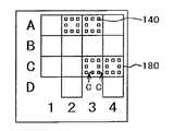
액정 표시 장치는, 다수의 TFT 기판(100)이 형성된 마더 TFT 기판 및 다수의 대향 기판(200)이 형성된 마더 대향 기판을 부착하여 마더 기판으로 하고, 그 후, 스크라이빙 등에 의해 개개의 액정 표시 패널로 분리하는 것이 행해지고 있다. 마더 TFT 기판과 마더 대향 기판을 시일재를 통해 접착할 때에 위치 정렬 마크(180)가 필요하다.The liquid crystal display device attaches a mother TFT substrate on which a plurality of
도 7은 위치 정렬 마크(180)의 예이다. 도 7에 있어서, 위치 정렬 마크(180)는 정사각형의 유닛의 조합으로 형성되어 있다. 위치 정렬 마크(180)의 유닛의 일부에는, 직사각형 형상의 가스 배출을 위한 스루홀(140)이 형성되어 있다. 이 스루홀은 제2 층간 절연막(111)에 형성되어 있다. 이 가스 배출을 위한 스루홀(140)에 의해 유기 패시베이션막(109)에 흡수된 수분 등의 방출을 쉽게 하여, 제2 층간 절연막(111)의 박리를 방지하고 있다.7 is an example of the
도 8은, 도 7에 있어서의 C-C 단면이다. 도 8은, 반도체층(103)이 없는 것 이외에는 도 6에 기재한 것과 마찬가지의 구성이기 때문에, 설명은 생략한다. 또한, 도 6 또는 도 8은 단면의 예이며, 도 6에서 반도체층(103)이 항상 존재하고, 도 8에서 반도체층(103)이 항상 존재하지 않는다는 것은 아니다.8 is a cross-sectional view taken along the line C-C in FIG. 7. Since FIG. 8 is the structure similar to what was described in FIG. 6 except having no
이상과 같이, 액정 표시 패널에 있어서의 액정이 밀봉된 영역 이외에도 유기 패시베이션막(109) 및 제2 층간 절연막(111)이 형성되어 있는 경우에는, 이 부분의 제2 층간 절연막(111)에도 가스 배출을 위한 스루홀(140)을 형성함으로써 TEG(170) 또는 위치 정렬 마크(180)로서의 역할을 확실하게 달성시킬 수 있다. 또한, 도 1에 도시하는 TEG(170) 또는 위치 정렬 마크(180)는, 액정 표시 장치가 완성된 후에는 필요가 없어지기 때문에 이 부분을 스크라이브를 행할 때에 제거하는 경우도 많다.As described above, when the
또한, 본 실시예에 있어서도, 제2 층간 절연막(111)에 형성된 가스 배출을 위한 스루홀(140)은 ITO에 의해 덮여 있지 않다. 따라서, 유기 패시베이션막으로부터 방출되는 가스를 더 효과적으로 외부로 방출할 수 있다.Also, in this embodiment, the through
이상의 예에서는, 유기 패시베이션막(109) 위에 커먼 전극(110)을 형성하고, 그 위에 제 2 층간 절연막(111)을 통해 슬릿(115)을 갖는 화소 전극(112)이 형성되어 있는 타입의 IPS에 대하여 설명하였다. 그러나, 본 발명은, 유기 패시베이션막(109) 위에 화소 전극(112)을 형성하고, 그 위에 제 2 층간 절연막(111)을 통해 슬릿(115)을 갖는 커먼 전극을 배치하는 타입의 IPS에 대해서도 마찬가지로 적용할 수 있다.In the above example, in the IPS of the type in which the
10 : 표시 영역
20 : 시일재
30 : 주사 신호선
31 : 주사 신호선 인출선
40 : 영상 신호선
100 : TFT 기판
101 : 제1 하지막
102 : 제2 하지막
103 : 반도체층
104 : 게이트 절연막
105 : 게이트 전극
106 : 제1 층간 절연막
107 : 소스 전극
108 : 무기 패시베이션막
109 : 유기 패시베이션막
110 : 커먼 전극
111 : 제2 층간 절연막
112 : 화소 전극
113 : 배향막
115 : 슬릿
130 : 콘택트 홀
135 : 차광 전극
150 : 단자부
140 : 스루홀
160 : 상부 주변 회로
170 : TEG
180 : 위치 정렬 마크
200 : 대향 기판
201 : 컬러 필터
202 : 블랙 매트릭스
203 : 오버 코트막
210 : 외부 도전막
300 : 액정층
301 : 액정 분자
S : 소스부
D : 드레인부10: display area
20: sealing material
30: scanning signal line
31: scanning signal line leader
40: video signal line
100: TFT substrate
101: first lower film
102: second base film
103: semiconductor layer
104: gate insulating film
105: gate electrode
106: first interlayer insulating film
107 source electrode
108: weapon passivation film
109 organic passivation film
110: common electrode
111: second interlayer insulating film
112: pixel electrode
113: alignment layer
115: slit
130: contact hole
135: light blocking electrode
150: terminal portion
140: through hole
160: upper peripheral circuit
170: TEG
180: position alignment mark
200: opposing substrate
201: color filter
202: black matrix
203: overcoat film
210: outer conductive film
300: liquid crystal layer
301: liquid crystal molecules
S: sauce part
D: drain part
Claims (8)
Translated fromKorean상기 TFT는 채널부와 상기 영상 신호선측에 형성된 드레인부와 상기 화소 전극측에 형성된 소스부를 갖는 반도체층과, 상기 반도체층을 덮어서 게이트 절연막이 형성되고, 상기 게이트 절연막 위이며 또한 상기 채널부의 상측에 형성된 게이트 전극과, 상기 게이트 전극을 덮는 제1 층간 절연막에 의해 형성되고,
상기 영상 신호선은 상기 제1 층간 절연막 위에 배치하고,
상기 영상 신호선을 덮어서 무기 패시베이션막과 유기 패시베이션막이 이 순서대로 형성되고, 상기 유기 패시베이션막 위에 커먼 전극이 형성되고, 상기 커먼 전극 위에 제2 층간 절연막이 형성되고, 상기 제2 층간 절연막 위에 상기 화소 전극이 형성되고, 상기 화소 전극은 슬릿을 갖고,
상기 영상 신호선은 상기 TFT의 상기 드레인부와 접속하는 부분은 폭이 넓게 형성되고, 상기 영상 신호선은 상기 폭이 넓어진 부분에서 콘택트 홀을 통해 상기 드레인부와 접속하고,
상기 영상 신호선의 폭이 넓어진 부분에서 상기 제2 층간 절연막에 스루홀이 형성되고, 상기 스루홀의 직경은 상기 콘택트 홀의 직경보다 큰 것을 특징으로 하는 액정 표시 장치.A pixel electrode is formed in an area surrounded by a scanning line extending in a first direction and arranged in a second direction and an image signal line extending in a second direction and arranged in the first direction, and the pixel electrode is connected to the image from the image signal line through a TFT. A liquid crystal display device to which a signal is supplied,
The TFT includes a semiconductor layer having a channel portion, a drain portion formed on the side of the image signal line, and a source portion formed on the pixel electrode side, and a gate insulating film covering the semiconductor layer to be formed on the gate insulating film and above the channel portion. A gate electrode formed and a first interlayer insulating film covering the gate electrode,
The image signal line is disposed on the first interlayer insulating layer,
An inorganic passivation film and an organic passivation film are formed in this order by covering the image signal line, a common electrode is formed on the organic passivation film, a second interlayer insulating film is formed on the common electrode, and the pixel electrode is formed on the second interlayer insulating film. Is formed, and the pixel electrode has a slit,
The portion of the video signal line which is connected to the drain portion of the TFT is formed to have a wide width, and the image signal line is connected to the drain portion via a contact hole at the portion of which the width is widened.
A through hole is formed in the second interlayer insulating layer in a portion where the width of the image signal line is widened, and the diameter of the through hole is larger than the diameter of the contact hole.
상기 TFT는 상기 영상 신호선과 접속하는 드레인부를 갖는 제1 TFT와, 상기 제1 TFT와 접속하고, 소스부가 화소 전극과 접속하는 제2 TFT로부터 구성되며, 상기 제1 TFT와 상기 제2 TFT의 게이트 전극은 상기 주사선이 겸하고 있는 것을 특징으로 하는 액정 표시 장치.The method of claim 1,
The TFT is composed of a first TFT having a drain portion connected to the video signal line, and a second TFT connected to the first TFT, and a source portion connected to a pixel electrode, the gate of the first TFT and the second TFT. An electrode is a liquid crystal display device, which serves as the scan line.
상기 TFT는 채널부와 상기 영상 신호선측에 형성된 드레인부와 상기 화소 전극측에 형성된 소스부를 갖는 반도체층과, 상기 반도체층을 덮어서 게이트 절연막이 형성되고, 상기 게이트 절연막 위이며 또한 상기 채널부의 상측에 형성된 게이트 전극과, 상기 게이트 전극을 덮는 제1 층간 절연막에 의해 형성되고,
상기 영상 신호선은 상기 제1 층간 절연막 위에 배치하고,
상기 영상 신호선을 덮어서 무기 패시베이션막과 유기 패시베이션막이 이 순서대로 형성되고, 상기 유기 패시베이션막 위에 화소 전극이 형성되고, 상기 화소 전극 위에 제2 층간 절연막이 형성되고, 상기 제2 층간 절연막 위에 커먼 전극이 형성되고, 상기 커먼 전극은 슬릿을 갖고,
상기 영상 신호선은 상기 TFT의 상기 드레인부와 접속하는 부분은 폭이 넓게 형성되고, 상기 영상 신호선은 상기 폭이 넓어진 부분에서 콘택트 홀을 통해 상기 드레인부와 접속하고,
상기 영상 신호선의 폭이 넓어진 부분에서 상기 제2 층간 절연막에 스루홀이 형성되고, 상기 스루홀의 직경은 상기 콘택트 홀의 직경보다 큰 것을 특징으로 하는 액정 표시 장치.A pixel electrode is formed in an area surrounded by a scanning line extending in a first direction and arranged in a second direction and an image signal line extending in a second direction and arranged in the first direction, and the pixel electrode is connected to the image from the image signal line through a TFT. A liquid crystal display device to which a signal is supplied,
The TFT includes a semiconductor layer having a channel portion, a drain portion formed on the side of the image signal line, and a source portion formed on the pixel electrode side, and a gate insulating film covering the semiconductor layer to be formed on the gate insulating film and above the channel portion. A gate electrode formed and a first interlayer insulating film covering the gate electrode,
The image signal line is disposed on the first interlayer insulating layer,
An inorganic passivation film and an organic passivation film are formed in this order to cover the video signal line, a pixel electrode is formed on the organic passivation film, a second interlayer insulating film is formed on the pixel electrode, and a common electrode is formed on the second interlayer insulating film. Formed, the common electrode has a slit,
The portion of the video signal line which is connected to the drain portion of the TFT is formed to have a wide width, and the image signal line is connected to the drain portion via a contact hole at the portion of which the width is widened.
A through hole is formed in the second interlayer insulating layer in a portion where the width of the image signal line is widened, and the diameter of the through hole is larger than the diameter of the contact hole.
상기 TFT는 상기 영상 신호선과 접속하는 드레인부를 갖는 제1 TFT와, 상기 제1 TFT와 접속하고, 소스부가 화소 전극과 접속하는 제2 TFT로부터 구성되며, 상기 제1 TFT와 상기 제2 TFT의 게이트 전극은 상기 주사선이 겸하고 있는 것을 특징으로 하는 액정 표시 장치.The method of claim 3,
The TFT is composed of a first TFT having a drain portion connected to the video signal line, and a second TFT connected to the first TFT, and a source portion connected to a pixel electrode, the gate of the first TFT and the second TFT. An electrode is a liquid crystal display device, which serves as the scan line.
상기 주변 회로부는 채널부와 소스부와 드레인부를 갖는 반도체층과, 상기 반도체층을 덮어서 게이트 절연막이 형성되고, 상기 게이트 절연막 위이며 또한 상기 채널부의 상측에 형성된 게이트 전극과, 상기 게이트 전극을 덮는 제1 층간 절연막에 의해 형성된 TFT를 갖고,
상기 제1 층간 절연막 위에 금속에 의한 배선이 형성되고, 상기 금속에 의한 배선은 상기 제1 층간 절연막 및 게이트 절연막에 형성된 콘택트 홀을 통해 상기 드레인부 또는 상기 소스부와 접속하고,
상기 금속에 의한 배선을 덮어서 무기 패시베이션막과 유기 패시베이션막이 이 순서대로 형성되고,
상기 유기 패시베이션막 위에 ITO로 이루어지는 배선이 형성되고, 상기 ITO로 이루어지는 배선 위에 제2 층간 절연막이 형성되고, 상기 제2 층간 절연막에는 스루홀이 형성되고, 상기 스루홀의 직경은 상기 콘택트 홀의 직경보다 큰 것을 특징으로 하는 액정 표시 장치.A liquid crystal display device having a display area and a peripheral circuit portion,
The peripheral circuit portion includes a semiconductor layer having a channel portion, a source portion, and a drain portion, a gate insulating film covering the semiconductor layer, a gate electrode formed on the gate insulating film and above the channel portion, and covering the gate electrode. Has a TFT formed by an interlayer insulating film,
A metal wiring is formed on the first interlayer insulating film, and the metal wiring is connected to the drain portion or the source portion through a contact hole formed in the first interlayer insulating film and the gate insulating film;
An inorganic passivation film and an organic passivation film are formed in this order by covering the wiring by the metal.
A wiring made of ITO is formed on the organic passivation film, a second interlayer insulating film is formed on the wiring made of ITO, a through hole is formed in the second interlayer insulating film, and the diameter of the through hole is larger than the diameter of the contact hole. A liquid crystal display device, characterized in that.
상기 TEG에 있어서는 TFT 기판 위에 반도체층, 게이트 절연막, 제1 층간 절연막, 무기 패시베이션막, 유기 패시베이션막이 이 순서대로 적층되고,
상기 유기 패시베이션막 위에는 ITO로 형성된 전극이 형성되고, 상기 ITO로 형성된 전극 위에 제2 층간 절연막이 형성되고, 상기 제2 층간 절연막에는 상기 TEG가 형성되어 있는 영역에서 스루홀이 형성되어 있는 것을 특징으로 하는 액정 표시 장치.A liquid crystal display device in which a TFT substrate and an opposing substrate are opposed to each other, a liquid crystal layer is formed therein, and a terminal portion and a TEG are formed in a portion of the TFT substrate not facing the opposing electrode.
In the TEG, a semiconductor layer, a gate insulating film, a first interlayer insulating film, an inorganic passivation film, and an organic passivation film are stacked in this order on the TFT substrate,
An electrode formed of ITO is formed on the organic passivation film, a second interlayer insulating film is formed on the electrode formed of ITO, and a through hole is formed in a region where the TEG is formed on the second interlayer insulating film. Liquid crystal display.
상기 위치 정렬 마크에서는 TFT 기판 위에 게이트 절연막, 제1 층간 절연막, 무기 패시베이션막, 유기 패시베이션막이 이 순서대로 적층되고,
상기 유기 패시베이션막 위에는 ITO로 형성된 전극이 형성되고, 상기 ITO로 형성된 전극 위에 제2 층간 절연막이 형성되고, 상기 제2 층간 절연막에는 상기 위치 정렬 마크가 형성되어 있는 영역에서 스루홀이 형성되어 있는 것을 특징으로 하는 액정 표시 장치.A liquid crystal display device in which a TFT substrate and an opposing substrate are opposed to each other, a liquid crystal layer is formed therein, and a terminal portion and an alignment mark are formed in a portion of the TFT substrate not facing the opposing electrode.
In the positioning mark, a gate insulating film, a first interlayer insulating film, an inorganic passivation film, and an organic passivation film are stacked in this order on the TFT substrate,
An electrode formed of ITO is formed on the organic passivation film, a second interlayer insulating film is formed on the electrode formed of ITO, and a through hole is formed in a region where the alignment mark is formed on the second interlayer insulating film. A liquid crystal display device characterized by the above-mentioned.
상기 제2 층간 절연막에 형성된 상기 스루홀은 ITO에 의해 덮여 있지 않은 것을 특징으로 하는 액정 표시 장치.The method according to any one of claims 1 to 7,
And said through hole formed in said second interlayer insulating film is not covered by ITO.
Applications Claiming Priority (2)
| Application Number | Priority Date | Filing Date | Title |
|---|---|---|---|
| JP2010279155AJP5372900B2 (en) | 2010-12-15 | 2010-12-15 | Liquid crystal display |
| JPJP-P-2010-279155 | 2010-12-15 |
Publications (2)
| Publication Number | Publication Date |
|---|---|
| KR20120067288Atrue KR20120067288A (en) | 2012-06-25 |
| KR101322563B1 KR101322563B1 (en) | 2013-10-28 |
Family
ID=45491245
Family Applications (1)
| Application Number | Title | Priority Date | Filing Date |
|---|---|---|---|
| KR1020110131721AActiveKR101322563B1 (en) | 2010-12-15 | 2011-12-09 | Liquid crystal display device |
Country Status (6)
| Country | Link |
|---|---|
| US (3) | US8563982B2 (en) |
| EP (1) | EP2466365B1 (en) |
| JP (1) | JP5372900B2 (en) |
| KR (1) | KR101322563B1 (en) |
| CN (1) | CN102540603B (en) |
| TW (1) | TWI463214B (en) |
Cited By (4)
| Publication number | Priority date | Publication date | Assignee | Title |
|---|---|---|---|---|
| US9030620B2 (en) | 2013-06-14 | 2015-05-12 | Samsung Display Co., Ltd. | Display panel and method of manufacturing the same |
| US9097925B2 (en) | 2012-07-20 | 2015-08-04 | Semiconductor Energy Laboratory Co., Ltd. | Display device |
| US9298057B2 (en) | 2012-07-20 | 2016-03-29 | Semiconductor Energy Laboratory Co., Ltd. | Display device and electronic device including the display device |
| US9915844B2 (en) | 2015-06-08 | 2018-03-13 | Samsung Display Co., Ltd. | Liquid crystal display and method of manufacturing the same |
Families Citing this family (21)
| Publication number | Priority date | Publication date | Assignee | Title |
|---|---|---|---|---|
| JPWO2013008359A1 (en)* | 2011-07-13 | 2015-02-23 | パナソニック株式会社 | Liquid crystal display device and manufacturing method thereof |
| KR101900915B1 (en)* | 2011-10-14 | 2018-09-27 | 삼성디스플레이 주식회사 | Display device |
| US9046722B2 (en) | 2012-09-20 | 2015-06-02 | Shanghai Avic Optoelectronics Co., Ltd. | Method of fabricating In-Plane Switching (IPS) screen electrode |
| CN103676344B (en)* | 2012-09-20 | 2017-03-22 | 上海中航光电子有限公司 | Method for manufacturing IPS (In-panel Switching) screen electrode |
| JP5714676B2 (en)* | 2013-09-18 | 2015-05-07 | 株式会社ジャパンディスプレイ | Liquid crystal display device and manufacturing method thereof |
| KR102275519B1 (en)* | 2013-12-16 | 2021-07-12 | 삼성디스플레이 주식회사 | Display substrate and method of manufacturing the same |
| KR102150033B1 (en) | 2014-01-14 | 2020-10-15 | 삼성디스플레이 주식회사 | Array substrate, display panel having the same and method of manufacturing the same |
| KR102183564B1 (en) | 2014-04-23 | 2020-11-27 | 삼성디스플레이 주식회사 | Display device and manufacturing method thereof |
| TWI553388B (en)* | 2014-09-11 | 2016-10-11 | 群創光電股份有限公司 | Liquid crystal display device and component substrate thereof |
| CN106598314B (en)* | 2015-10-15 | 2023-07-04 | 京东方科技集团股份有限公司 | Embedded touch screen, display device and driving method of display device |
| WO2017063444A1 (en) | 2015-10-15 | 2017-04-20 | 京东方科技集团股份有限公司 | Touch panel, display device, and driving method therefor |
| CN205787504U (en) | 2016-05-31 | 2016-12-07 | 京东方科技集团股份有限公司 | A kind of array base palte and display device |
| JP6885134B2 (en)* | 2017-03-24 | 2021-06-09 | セイコーエプソン株式会社 | Electro-optic equipment, manufacturing method of electro-optic equipment, electronic equipment |
| GB2568515A (en)* | 2017-11-17 | 2019-05-22 | Flexenable Ltd | Display devices |
| US20200073155A1 (en)* | 2018-08-31 | 2020-03-05 | Sharp Kabushiki Kaisha | Electronic component board, display panel, and method of producing them |
| TWI688988B (en)* | 2018-11-01 | 2020-03-21 | 友達光電股份有限公司 | Device substrate and manufacturing mehod thereof |
| CN110673386A (en)* | 2019-10-15 | 2020-01-10 | 深圳市华星光电技术有限公司 | Array substrate and liquid crystal display panel |
| WO2022027506A1 (en)* | 2020-08-06 | 2022-02-10 | 京东方科技集团股份有限公司 | Display panel and display apparatus |
| CN115968590A (en)* | 2021-07-30 | 2023-04-14 | 京东方科技集团股份有限公司 | Array substrate and display device |
| JP7488807B2 (en) | 2021-11-30 | 2024-05-22 | シャープディスプレイテクノロジー株式会社 | Active matrix substrate, liquid crystal display device, and method for manufacturing active matrix substrate |
| CN116224642A (en)* | 2023-03-16 | 2023-06-06 | 惠科股份有限公司 | Color filter substrate and manufacturing method thereof, liquid crystal display panel and liquid crystal display device |
Family Cites Families (21)
| Publication number | Priority date | Publication date | Assignee | Title |
|---|---|---|---|---|
| JPH05121570A (en)* | 1991-10-25 | 1993-05-18 | Nec Corp | Semiconductor device |
| JP3625598B2 (en)* | 1995-12-30 | 2005-03-02 | 三星電子株式会社 | Manufacturing method of liquid crystal display device |
| JP2001324725A (en) | 2000-05-12 | 2001-11-22 | Hitachi Ltd | Liquid crystal display device and manufacturing method thereof |
| JP4041336B2 (en)* | 2001-06-29 | 2008-01-30 | シャープ株式会社 | Substrate for liquid crystal display device, liquid crystal display device including the same, and manufacturing method thereof |
| JP4199501B2 (en)* | 2002-09-13 | 2008-12-17 | Nec液晶テクノロジー株式会社 | Manufacturing method of liquid crystal display device |
| JP3722141B2 (en)* | 2002-12-20 | 2005-11-30 | セイコーエプソン株式会社 | ELECTRO-OPTICAL DEVICE WITH MOUNTING CASE, PROJECTION TYPE DISPLAY DEVICE, AND MOUNTING CASE |
| JP2004325953A (en)* | 2003-04-25 | 2004-11-18 | Nec Lcd Technologies Ltd | Liquid crystal display |
| KR100675631B1 (en) | 2003-06-27 | 2007-02-01 | 엘지.필립스 엘시디 주식회사 | Transverse electric field liquid crystal display device and manufacturing method thereof |
| JP2006018185A (en)* | 2004-07-05 | 2006-01-19 | Nec Lcd Technologies Ltd | Liquid crystal display |
| US7479655B2 (en)* | 2006-01-31 | 2009-01-20 | Semiconductor Energy Laboratory Co., Ltd. | Semiconductor device |
| JP4717672B2 (en)* | 2006-03-17 | 2011-07-06 | ソニー株式会社 | Liquid crystal device and electronic device |
| KR101331942B1 (en)* | 2007-05-03 | 2013-11-21 | 삼성디스플레이 주식회사 | Display device and method of manufacturing for the same |
| JP2009042292A (en) | 2007-08-06 | 2009-02-26 | Hitachi Displays Ltd | Liquid crystal display |
| US7916247B2 (en)* | 2007-08-30 | 2011-03-29 | Seiko Epson Corporation | Electro-optic device, and electronic apparatus including the same |
| EP2230658A4 (en)* | 2008-01-09 | 2011-09-14 | Sharp Kk | Display device |
| JP2009271103A (en)* | 2008-04-30 | 2009-11-19 | Hitachi Displays Ltd | Liquid crystal display device |
| JP5121570B2 (en) | 2008-05-23 | 2013-01-16 | 日本圧着端子製造株式会社 | Connector terminal and connector provided with this connector terminal |
| JP5172508B2 (en) | 2008-07-09 | 2013-03-27 | 株式会社ジャパンディスプレイセントラル | Liquid crystal display |
| JP5553513B2 (en)* | 2009-02-09 | 2014-07-16 | 株式会社ジャパンディスプレイ | Liquid crystal display device and manufacturing method thereof |
| JP5335628B2 (en) | 2009-09-09 | 2013-11-06 | 株式会社ジャパンディスプレイ | Liquid crystal display |
| JP5193328B2 (en)* | 2011-03-02 | 2013-05-08 | 株式会社ジャパンディスプレイイースト | Liquid crystal display |
- 2010
- 2010-12-15JPJP2010279155Apatent/JP5372900B2/enactiveActive
- 2011
- 2011-11-29TWTW100143788Apatent/TWI463214B/enactive
- 2011-12-06USUS13/311,595patent/US8563982B2/enactiveActive
- 2011-12-09KRKR1020110131721Apatent/KR101322563B1/enactiveActive
- 2011-12-14CNCN201110430612.0Apatent/CN102540603B/enactiveActive
- 2011-12-14EPEP11193409.7Apatent/EP2466365B1/enactiveActive
- 2013
- 2013-10-17USUS14/056,545patent/US9170463B2/enactiveActive
- 2015
- 2015-07-07USUS14/746,102patent/US9568795B2/enactiveActive
Cited By (20)
| Publication number | Priority date | Publication date | Assignee | Title |
|---|---|---|---|---|
| US10877338B2 (en) | 2012-07-20 | 2020-12-29 | Semiconductor Energy Laboratory Co., Ltd. | Display device |
| US9097925B2 (en) | 2012-07-20 | 2015-08-04 | Semiconductor Energy Laboratory Co., Ltd. | Display device |
| US9298057B2 (en) | 2012-07-20 | 2016-03-29 | Semiconductor Energy Laboratory Co., Ltd. | Display device and electronic device including the display device |
| US9366894B2 (en) | 2012-07-20 | 2016-06-14 | Semiconductor Energy Laboratory Co., Ltd. | Display device |
| US12210257B2 (en) | 2012-07-20 | 2025-01-28 | Semiconductor Energy Laboratory Co., Ltd. | Display device and electronic device including the display device |
| US10018887B2 (en) | 2012-07-20 | 2018-07-10 | Semiconductor Energy Laboratory Co., Ltd. | Display device |
| US10437091B2 (en) | 2012-07-20 | 2019-10-08 | Semiconductor Energy Laboratory Co., Ltd. | Display device |
| US10514580B2 (en) | 2012-07-20 | 2019-12-24 | Semiconductor Energy Laboratory Co., Ltd. | Display device and electronic device including the display device |
| US10852576B2 (en) | 2012-07-20 | 2020-12-01 | Semiconductor Energy Laboratory Co., Ltd. | Display device |
| US10514579B2 (en) | 2012-07-20 | 2019-12-24 | Semiconductor Energy Laboratory Co., Ltd. | Display device and electronic device including the display device |
| US11209710B2 (en) | 2012-07-20 | 2021-12-28 | Semiconductor Energy Laboratory Co., Ltd. | Display device and electronic device including the display device |
| US11137651B2 (en) | 2012-07-20 | 2021-10-05 | Semiconductor Energy Laboratory Co., Ltd. | Display device |
| US12117704B2 (en) | 2012-07-20 | 2024-10-15 | Semiconductor Energy Laboratory Co., Ltd. | Display device |
| US11327376B2 (en) | 2012-07-20 | 2022-05-10 | Semiconductor Energy Laboratory Co., Ltd. | Display device |
| US11531243B2 (en) | 2012-07-20 | 2022-12-20 | Semiconductor Energy Laboratory Co., Ltd. | Display device and electronic device including the display device |
| US11543718B2 (en) | 2012-07-20 | 2023-01-03 | Semiconductor Energy Laboratory Co., Ltd. | Display device |
| US11841595B2 (en) | 2012-07-20 | 2023-12-12 | Semiconductor Energy Laboratory Co., Ltd. | Display device |
| US11899328B2 (en) | 2012-07-20 | 2024-02-13 | Semiconductor Energy Laboratory Co., Ltd. | Display device and electronic device including the display device |
| US9030620B2 (en) | 2013-06-14 | 2015-05-12 | Samsung Display Co., Ltd. | Display panel and method of manufacturing the same |
| US9915844B2 (en) | 2015-06-08 | 2018-03-13 | Samsung Display Co., Ltd. | Liquid crystal display and method of manufacturing the same |
Also Published As
| Publication number | Publication date |
|---|---|
| JP5372900B2 (en) | 2013-12-18 |
| US20160011478A1 (en) | 2016-01-14 |
| KR101322563B1 (en) | 2013-10-28 |
| EP2466365A3 (en) | 2012-09-26 |
| JP2012128159A (en) | 2012-07-05 |
| TWI463214B (en) | 2014-12-01 |
| US20140043555A1 (en) | 2014-02-13 |
| TW201229627A (en) | 2012-07-16 |
| EP2466365A2 (en) | 2012-06-20 |
| US9170463B2 (en) | 2015-10-27 |
| US20120153292A1 (en) | 2012-06-21 |
| US9568795B2 (en) | 2017-02-14 |
| US8563982B2 (en) | 2013-10-22 |
| CN102540603B (en) | 2015-06-17 |
| EP2466365B1 (en) | 2013-09-18 |
| CN102540603A (en) | 2012-07-04 |
Similar Documents
| Publication | Publication Date | Title |
|---|---|---|
| KR101322563B1 (en) | Liquid crystal display device | |
| JP5335628B2 (en) | Liquid crystal display | |
| US9612487B2 (en) | Array substrate, manufacturing method thereof and display device | |
| US20200301181A1 (en) | Liquid crystal display device | |
| TWI574081B (en) | Liquid crystal display device and manufacturing method thereof | |
| CN104749841B (en) | Thin-film transistor array base-plate and its manufacture method | |
| JP6340193B2 (en) | Liquid crystal display | |
| US8531637B2 (en) | Liquid crystal display device and manufacturing method thereof | |
| US20240162245A1 (en) | Array substrate, method for manufacturing array substrate and display panel | |
| KR20130053592A (en) | Thin film transistor substrate and method of fabricating the same | |
| JP5714676B2 (en) | Liquid crystal display device and manufacturing method thereof | |
| US9703152B2 (en) | Liquid crystal display device | |
| KR102084398B1 (en) | Liquid crystal display device and method of fabricating the same | |
| KR101747721B1 (en) | Liquid crystal display device and manufacturing method thereof | |
| WO2017031805A1 (en) | Array substrate and display device | |
| US11294249B2 (en) | Liquid crystal display panel and manufacturing method | |
| JP2013127562A (en) | Liquid crystal display device and method for manufacturing the same | |
| KR101264864B1 (en) | Liquid crystal display device and manufacturing method thereof | |
| JP2011164199A (en) | Liquid crystal display device | |
| KR20160092423A (en) | Color filter array substrate and method for fabricating the same, and liquid crystal display device and method for fabricating the same | |
| KR20140076919A (en) | Thin film transistor array substrate | |
| JP2012242496A (en) | Liquid crystal display |
Legal Events
| Date | Code | Title | Description |
|---|---|---|---|
| A201 | Request for examination | ||
| PA0109 | Patent application | St.27 status event code:A-0-1-A10-A12-nap-PA0109 | |
| PA0201 | Request for examination | St.27 status event code:A-1-2-D10-D11-exm-PA0201 | |
| PN2301 | Change of applicant | St.27 status event code:A-3-3-R10-R13-asn-PN2301 St.27 status event code:A-3-3-R10-R11-asn-PN2301 | |
| PG1501 | Laying open of application | St.27 status event code:A-1-1-Q10-Q12-nap-PG1501 | |
| D13-X000 | Search requested | St.27 status event code:A-1-2-D10-D13-srh-X000 | |
| D14-X000 | Search report completed | St.27 status event code:A-1-2-D10-D14-srh-X000 | |
| R18-X000 | Changes to party contact information recorded | St.27 status event code:A-3-3-R10-R18-oth-X000 | |
| E902 | Notification of reason for refusal | ||
| PE0902 | Notice of grounds for rejection | St.27 status event code:A-1-2-D10-D21-exm-PE0902 | |
| P11-X000 | Amendment of application requested | St.27 status event code:A-2-2-P10-P11-nap-X000 | |
| P13-X000 | Application amended | St.27 status event code:A-2-2-P10-P13-nap-X000 | |
| E701 | Decision to grant or registration of patent right | ||
| PE0701 | Decision of registration | St.27 status event code:A-1-2-D10-D22-exm-PE0701 | |
| GRNT | Written decision to grant | ||
| PR0701 | Registration of establishment | St.27 status event code:A-2-4-F10-F11-exm-PR0701 | |
| PR1002 | Payment of registration fee | St.27 status event code:A-2-2-U10-U11-oth-PR1002 Fee payment year number:1 | |
| PG1601 | Publication of registration | St.27 status event code:A-4-4-Q10-Q13-nap-PG1601 | |
| PR1001 | Payment of annual fee | St.27 status event code:A-4-4-U10-U11-oth-PR1001 Fee payment year number:4 | |
| PR1001 | Payment of annual fee | St.27 status event code:A-4-4-U10-U11-oth-PR1001 Fee payment year number:5 | |
| PR1001 | Payment of annual fee | St.27 status event code:A-4-4-U10-U11-oth-PR1001 Fee payment year number:6 | |
| PR1001 | Payment of annual fee | St.27 status event code:A-4-4-U10-U11-oth-PR1001 Fee payment year number:7 | |
| PR1001 | Payment of annual fee | St.27 status event code:A-4-4-U10-U11-oth-PR1001 Fee payment year number:8 | |
| PR1001 | Payment of annual fee | St.27 status event code:A-4-4-U10-U11-oth-PR1001 Fee payment year number:9 | |
| PR1001 | Payment of annual fee | St.27 status event code:A-4-4-U10-U11-oth-PR1001 Fee payment year number:10 | |
| PR1001 | Payment of annual fee | St.27 status event code:A-4-4-U10-U11-oth-PR1001 Fee payment year number:11 | |
| PR1001 | Payment of annual fee | St.27 status event code:A-4-4-U10-U11-oth-PR1001 Fee payment year number:12 | |
| PN2301 | Change of applicant | St.27 status event code:A-5-5-R10-R11-asn-PN2301 | |
| PN2301 | Change of applicant | St.27 status event code:A-5-5-R10-R14-asn-PN2301 |