KR20120065854A - Method of fabricating oxide thin film transistor - Google Patents
Method of fabricating oxide thin film transistorDownload PDFInfo
- Publication number
- KR20120065854A KR20120065854AKR1020100127171AKR20100127171AKR20120065854AKR 20120065854 AKR20120065854 AKR 20120065854AKR 1020100127171 AKR1020100127171 AKR 1020100127171AKR 20100127171 AKR20100127171 AKR 20100127171AKR 20120065854 AKR20120065854 AKR 20120065854A
- Authority
- KR
- South Korea
- Prior art keywords
- insulating layer
- etch stopper
- layer
- active layer
- substrate
- Prior art date
- Legal status (The legal status is an assumption and is not a legal conclusion. Google has not performed a legal analysis and makes no representation as to the accuracy of the status listed.)
- Withdrawn
Links
Images


Classifications
- H—ELECTRICITY
- H10—SEMICONDUCTOR DEVICES; ELECTRIC SOLID-STATE DEVICES NOT OTHERWISE PROVIDED FOR
- H10D—INORGANIC ELECTRIC SEMICONDUCTOR DEVICES
- H10D30/00—Field-effect transistors [FET]
- H10D30/60—Insulated-gate field-effect transistors [IGFET]
- H10D30/67—Thin-film transistors [TFT]
- H10D30/674—Thin-film transistors [TFT] characterised by the active materials
- H10D30/6755—Oxide semiconductors, e.g. zinc oxide, copper aluminium oxide or cadmium stannate
- H—ELECTRICITY
- H10—SEMICONDUCTOR DEVICES; ELECTRIC SOLID-STATE DEVICES NOT OTHERWISE PROVIDED FOR
- H10D—INORGANIC ELECTRIC SEMICONDUCTOR DEVICES
- H10D30/00—Field-effect transistors [FET]
- H10D30/01—Manufacture or treatment
- H10D30/021—Manufacture or treatment of FETs having insulated gates [IGFET]
- H10D30/031—Manufacture or treatment of FETs having insulated gates [IGFET] of thin-film transistors [TFT]
- H—ELECTRICITY
- H10—SEMICONDUCTOR DEVICES; ELECTRIC SOLID-STATE DEVICES NOT OTHERWISE PROVIDED FOR
- H10D—INORGANIC ELECTRIC SEMICONDUCTOR DEVICES
- H10D30/00—Field-effect transistors [FET]
- H10D30/60—Insulated-gate field-effect transistors [IGFET]
- H10D30/67—Thin-film transistors [TFT]
- H10D30/6704—Thin-film transistors [TFT] having supplementary regions or layers in the thin films or in the insulated bulk substrates for controlling properties of the device
- H—ELECTRICITY
- H10—SEMICONDUCTOR DEVICES; ELECTRIC SOLID-STATE DEVICES NOT OTHERWISE PROVIDED FOR
- H10D—INORGANIC ELECTRIC SEMICONDUCTOR DEVICES
- H10D86/00—Integrated devices formed in or on insulating or conducting substrates, e.g. formed in silicon-on-insulator [SOI] substrates or on stainless steel or glass substrates
- H10D86/40—Integrated devices formed in or on insulating or conducting substrates, e.g. formed in silicon-on-insulator [SOI] substrates or on stainless steel or glass substrates characterised by multiple TFTs
- H10D86/421—Integrated devices formed in or on insulating or conducting substrates, e.g. formed in silicon-on-insulator [SOI] substrates or on stainless steel or glass substrates characterised by multiple TFTs having a particular composition, shape or crystalline structure of the active layer
- H10D86/423—Integrated devices formed in or on insulating or conducting substrates, e.g. formed in silicon-on-insulator [SOI] substrates or on stainless steel or glass substrates characterised by multiple TFTs having a particular composition, shape or crystalline structure of the active layer comprising semiconductor materials not belonging to the Group IV, e.g. InGaZnO
- H—ELECTRICITY
- H10—SEMICONDUCTOR DEVICES; ELECTRIC SOLID-STATE DEVICES NOT OTHERWISE PROVIDED FOR
- H10D—INORGANIC ELECTRIC SEMICONDUCTOR DEVICES
- H10D86/00—Integrated devices formed in or on insulating or conducting substrates, e.g. formed in silicon-on-insulator [SOI] substrates or on stainless steel or glass substrates
- H10D86/40—Integrated devices formed in or on insulating or conducting substrates, e.g. formed in silicon-on-insulator [SOI] substrates or on stainless steel or glass substrates characterised by multiple TFTs
- H10D86/60—Integrated devices formed in or on insulating or conducting substrates, e.g. formed in silicon-on-insulator [SOI] substrates or on stainless steel or glass substrates characterised by multiple TFTs wherein the TFTs are in active matrices
Landscapes
- Thin Film Transistor (AREA)
Abstract
Translated fromKoreanDescription
Translated fromKorean본 발명은 산화물 박막 트랜지스터의 제조방법에 관한 것으로, 보다 상세하게는 AxByCzO (A, B, C = Zn, Cd, Ga, In, Sn, Hf, Zr; x, y, z ≥ 0)의 조합으로 이루어진 삼성분계 또는 사성분계 산화물 반도체를 액티브층으로 사용한 산화물 박막 트랜지스터의 제조방법에 관한 것이다.BACKGROUND OF THE INVENTION 1. Field of the Invention The present invention relates to a method for manufacturing an oxide thin film transistor, and more particularly, in combination with AxByCzO (A, B, C = Zn, Cd, Ga, In, Sn, Hf, Zr; x, y, z ≥ 0). The present invention relates to a method for manufacturing an oxide thin film transistor using an integrative quarter- or tetracomponent oxide semiconductor as an active layer.
최근 정보 디스플레이에 관한 관심이 고조되고 휴대가 가능한 정보매체를 이용하려는 요구가 높아지면서 기존의 표시장치인 브라운관(Cathode Ray Tube; CRT)을 대체하는 경량 박막형 평판표시장치(Flat Panel Display; FPD)에 대한 연구 및 상업화가 중점적으로 이루어지고 있다. 특히, 이러한 평판표시장치 중 액정표시장치(Liquid Crystal Display; LCD)는 액정의 광학적 이방성을 이용하여 이미지를 표현하는 장치로서, 해상도와 컬러표시 및 화질 등에서 우수하여 노트북이나 데스크탑 모니터 등에 활발하게 적용되고 있다.Recently, with increasing interest in information display and increasing demand for using a portable information carrier, a lightweight flat panel display (FPD), which replaces a conventional display device, a cathode ray tube (CRT), is used. The research and commercialization of Korea is focused on. In particular, the liquid crystal display (LCD) of the flat panel display device is an image representing the image using the optical anisotropy of the liquid crystal, is excellent in resolution, color display and image quality, and is actively applied to notebooks or desktop monitors have.
상기 액정표시장치는 크게 컬러필터(color filter) 기판과 어레이(array) 기판 및 상기 컬러필터 기판과 어레이 기판 사이에 형성된 액정층(liquid crystal layer)으로 구성된다.The liquid crystal display is largely composed of a color filter substrate and an array substrate, and a liquid crystal layer formed between the color filter substrate and the array substrate.
상기 액정표시장치에 주로 사용되는 구동 방식인 능동 매트릭스(Active Matrix; AM) 방식은 비정질 실리콘 박막 트랜지스터(Amorphous Silicon Thin Film Transistor; a-Si TFT)를 스위칭소자로 사용하여 화소부의 액정을 구동하는 방식이다.The active matrix (AM) method, which is a driving method mainly used in the liquid crystal display device, uses an amorphous silicon thin film transistor (a-Si TFT) as a switching device to drive the liquid crystal in the pixel portion. to be.
이하, 도 1을 참조하여 일반적인 액정표시장치의 구조에 대해서 상세히 설명한다.Hereinafter, a structure of a general liquid crystal display device will be described in detail with reference to FIG. 1.
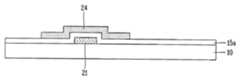
도 1은 일반적인 액정표시장치를 개략적으로 나타내는 분해사시도이다.1 is an exploded perspective view schematically illustrating a general liquid crystal display.
도면에 도시된 바와 같이, 상기 액정표시장치는 크게 컬러필터 기판(5)과 어레이 기판(10) 및 상기 컬러필터 기판(5)과 어레이 기판(10) 사이에 형성된 액정층(liquid crystal layer)(30)으로 구성된다.As shown in the figure, the liquid crystal display device is largely a liquid crystal layer (liquid crystal layer) formed between the
상기 컬러필터 기판(5)은 적(Red; R), 녹(Green; G) 및 청(Blue; B)의 색상을 구현하는 다수의 서브-컬러필터(7)로 구성된 컬러필터(C)와 상기 서브-컬러필터(7) 사이를 구분하고 액정층(30)을 투과하는 광을 차단하는 블랙매트릭스(black matrix)(6), 그리고 상기 액정층(30)에 전압을 인가하는 투명한 공통전극(8)으로 이루어져 있다.The
또한, 상기 어레이 기판(10)은 종횡으로 배열되어 복수개의 화소영역(P)을 정의하는 복수개의 게이트라인(16)과 데이터라인(17), 상기 게이트라인(16)과 데이터라인(17)의 교차영역에 형성된 스위칭소자인 박막 트랜지스터(T) 및 상기 화소영역(P) 위에 형성된 화소전극(18)으로 이루어져 있다.In addition, the
상기의 컬러필터 기판(5)과 어레이 기판(10)은 화상표시 영역의 외곽에 형성된 실런트(sealant)(미도시)에 의해 대향하도록 합착되어 액정표시패널을 구성하며, 상기 컬러필터 기판(5)과 어레이 기판(10)의 합착은 상기 컬러필터 기판(5) 또는 어레이 기판(10)에 형성된 합착키(미도시)를 통해 이루어진다.The
한편, 전술한 액정표시장치는 가볍고 전력소모가 작아 지금가지 가장 주목받는 디스플레이 소자지만, 상기 액정표시장치는 발광소자가 아니라 수광소자이며 밝기, 명암비(contrast ratio) 및 시야각 등에 기술적 한계가 있기 때문에 이러한 단점을 극복할 수 있는 새로운 디스플레이 소자에 대한 개발이 활발하게 전개되고 있다.On the other hand, the above-mentioned liquid crystal display device is the most attracting display device until now because of the light weight and low power consumption, but the liquid crystal display device is not a light emitting device, but a light receiving device and because of technical limitations such as brightness, contrast ratio and viewing angle, Development of new display devices that can overcome the disadvantages is actively being developed.
새로운 평판표시장치 중 하나인 유기전계발광소자(Organic Light Emitting Diode; OLED)는 자체발광형이기 때문에 액정표시장치에 비해 시야각과 명암비 등이 우수하며 백라이트(backlight)가 필요하지 않기 때문에 경량 박형이 가능하고, 소비전력 측면에서도 유리하다. 그리고, 직류 저전압 구동이 가능하고 응답속도가 빠르다는 장점이 있으며, 특히 제조비용 측면에서도 유리한 장점을 가지고 있다.Organic Light Emitting Diode (OLED), one of the new flat panel displays, is self-luminous, so it has better viewing angle and contrast ratio than liquid crystal displays, and it is lightweight because it does not require backlight. It is also advantageous in terms of power consumption. In addition, there is an advantage that the DC low-voltage drive is possible and the response speed is fast, in particular, it has an advantage in terms of manufacturing cost.
최근 유기전계발광 디스플레이의 대면적화에 관한 연구가 활발하게 진행되고 있으며, 이를 달성하기 위하여 유기전계발광소자의 구동 트랜지스터로서 정전류 특성을 확보하여 안정된 작동 및 내구성이 확보된 박막 트랜지스터 개발이 요구되고 있다.Recently, research on the large area of the organic light emitting display has been actively conducted, and in order to achieve this, there is a demand for developing a thin film transistor having a stable current and stable operation as a driving transistor of the organic light emitting display.
전술한 액정표시장치에 사용되는 비정질 실리콘 박막 트랜지스터는 저온 공정에서 제작할 수 있지만 이동도(mobility)가 매우 작고 정전류 테스트(constant current bias) 조건을 만족하지 않는다. 반면에 다결정 실리콘 박막 트랜지스터는 높은 이동도와 만족스러운 정전류 테스트 조건을 가지는 반면에 균일한 특성 확보가 어려워 대면적화가 어렵고 고온 공정이 필요하다.Amorphous silicon thin film transistors used in the above-described liquid crystal display device can be fabricated in a low temperature process, but have very low mobility and do not satisfy the constant current bias condition. Polycrystalline silicon thin film transistors, on the other hand, have high mobility and satisfactory constant current test conditions, and are difficult to obtain uniform characteristics, making it difficult to large area and require high temperature processes.
이에 산화물 반도체로 액티브층을 형성한 산화물 박막 트랜지스터가 개발되고 있는데, 이때 상기 산화물 반도체를 기존의 하부 게이트(bottom gate) 구조의 박막 트랜지스터에 적용하는 경우 소오스/드레인전극의 식각공정, 특히 플라즈마를 이용한 건식각(dry etching) 중에 산화물 반도체가 손상을 받아 변성을 일으키는 문제점이 있다.Accordingly, an oxide thin film transistor having an active layer formed of an oxide semiconductor has been developed. In this case, when the oxide semiconductor is applied to a thin film transistor having a bottom gate structure, an etching process of a source / drain electrode, in particular, plasma is used. There is a problem in that the oxide semiconductor is damaged during dry etching, causing denaturation.
이를 방지하기 위해 배리어 층(barrier layer)으로 에치 스타퍼(etch stopper)를 액티브층 상부에 추가로 형성하기도 하는데, 이 경우에도 액티브층의 백 채널(back channel)영역이 액티브층과 에치 스타퍼를 형성하기 위한 포토리소그래피(photolithography)공정(이하, 포토공정이라 함)에 사용되는 감광막과 스트리퍼와 같은 화학물질 및 자외선(ultraviolet; UV)에 노출되어 산화물 반도체의 특성이 변하게 되어 소자특성의 저하를 유발하게 된다.In order to prevent this, an etch stopper may be additionally formed on the active layer as a barrier layer. In this case, the back channel region of the active layer may form the active layer and the etch stopper. Exposure to chemicals such as photoresist film and stripper and ultraviolet light (UV) used in photolithography process (hereinafter referred to as photo process) to change the characteristics of the oxide semiconductor, causing deterioration of device characteristics Done.
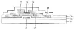
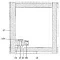
도 2는 일반적인 산화물 박막 트랜지스터의 구조를 개략적으로 나타내는 단면도이다.2 is a cross-sectional view schematically illustrating a structure of a general oxide thin film transistor.
도면에 도시된 바와 같이, 일반적인 산화물 박막 트랜지스터는 소정의 기판(10) 위에 형성된 게이트전극(21), 상기 게이트전극(21) 위에 형성된 게이트절연막(15a), 상기 게이트절연막(15a) 위에 산화물 반도체로 형성된 액티브층(24)과 소정의 절연물질로 형성된 에치 스타퍼(25), 상기 액티브층(24)의 소정영역과 전기적으로 접속하는 소오스/드레인전극(22, 23), 상기 소오스/드레인전극(22, 23) 위에 형성된 보호막(15b) 및 상기 드레인전극(23)과 전기적으로 접속하는 화소전극(18)으로 이루어져 있다.As shown in the drawing, a general oxide thin film transistor includes a
도 3a 내지 도 3f는 상기 도 2에 도시된 일반적인 산화물 박막 트랜지스터의 제조공정을 순차적으로 나타내는 단면도이다.3A through 3F are cross-sectional views sequentially illustrating a manufacturing process of the general oxide thin film transistor illustrated in FIG. 2.
도 3a에 도시된 바와 같이, 소정의 기판(10) 전면에 제 1 도전막을 증착한 후, 포토공정을 통해 선택적으로 패터닝함으로써 상기 기판(10) 위에 상기 제 1 도전막으로 이루어진 게이트전극(21)을 형성한다.As shown in FIG. 3A, a first conductive film is deposited on the entire surface of a
다음으로, 도 3b에 도시된 바와 같이, 상기 기판(10) 전면에 차례대로 게이트절연막(15a)과 소정의 산화물 반도체로 이루어진 산화물 반도체층을 증착한 후, 포토공정을 이용하여 선택적으로 패터닝함으로써 상기 게이트전극(21) 상부에 상기 산화물 반도체로 이루어진 액티브층(24)을 형성한다.Next, as illustrated in FIG. 3B, an oxide semiconductor layer including a
그리고, 도 3c에 도시된 바와 같이, 상기 기판(10) 전면에 소정의 절연물질로 이루어진 절연층을 증착한 후, 포토공정을 이용하여 선택적으로 패터닝함으로써 상기 액티브층(24) 상부에 상기 절연물질로 이루어진 에치 스타퍼(25)를 형성한다.As shown in FIG. 3C, an insulating layer made of a predetermined insulating material is deposited on the entire surface of the
다음으로, 도 3d에 도시된 바와 같이, 상기 에치 스타퍼(25)가 형성된 기판(10) 전면에 제 2 도전막을 형성한 후, 포토공정을 통해 선택적으로 패터닝함으로써 상기 액티브층(24)과 에치 스타퍼(25) 상부에 상기 제 2 도전막으로 이루어지며 상기 액티브층(24)의 소오스/드레인영역과 전기적으로 접속하는 소오스/드레인전극(22, 23)을 형성하게 된다.Next, as illustrated in FIG. 3D, a second conductive film is formed on the entire surface of the
다음으로, 도 3e에 도시된 바와 같이, 상기 소오스/드레인전극(22, 23)이 형성된 기판(10) 전면에 소정의 보호층(15b)을 형성한 후, 포토공정을 통해 선택적으로 패터닝함으로써 상기 드레인전극(23)의 일부를 노출시키는 콘택홀(40)을 형성하게 된다.Next, as shown in FIG. 3E, a predetermined
그리고, 도 3f에 도시된 바와 같이, 상기 기판(10) 전면에 제 3 도전막을 형성한 후, 포토공정을 통해 선택적으로 패터닝함으로써 상기 콘택홀을 통해 상기 드레인전극(23)과 전기적으로 접속하는 화소전극(18)을 형성하게 된다.As shown in FIG. 3F, a third conductive film is formed on the entire surface of the
즉, 종래기술은 산화물 반도체층의 증착 후, 포토공정을 통해 액티브층을 형성한 다음 에치 스타퍼를 형성하기 위한 절연층을 증착하게 된다. 그리고, 또 다른 포토공정을 통해 상기 절연층을 패터닝하여 에치 스타퍼를 형성하게 된다.That is, in the prior art, after the deposition of the oxide semiconductor layer, an active layer is formed through a photo process, and then an insulating layer for forming an etch stopper is deposited. In addition, the insulating layer is patterned through another photo process to form an etch stopper.
이때, 이러한 액티브층의 패터닝 및 절연층의 증착은 진공 챔버의 진공을 해제하고 나서 진행됨에 따라 산화물 반도체가 대기에 노출되는 한편, 액티브층과 에치 스타퍼를 패터닝하기 위한 포토공정을 거치면서 감광막과 스트리퍼와 같은 화학물질 및 UV에 노출됨으로써 백 채널영역이 손상을 받게 된다. 그 결과 소자특성이 저하되게 된다.At this time, the patterning of the active layer and the deposition of the insulating layer are performed after releasing the vacuum of the vacuum chamber, so that the oxide semiconductor is exposed to the atmosphere, and the photoresist film is subjected to a photo process for patterning the active layer and the etch stopper. Exposure to chemicals such as strippers and UV damage the back channel region. As a result, device characteristics are reduced.
일반적으로 산화물 반도체는 도체와 반도체의 2가지 특성을 모두 가지고 있으며, 박막 내 캐리어(carrier) 농도를 조절하여 전이시킬 수 있다. 상기 캐리어 농도를 조절하는 주 메커니즘(mechanism)은 산소 공격자점(空格子點)(vacancy)이 생성되며 만들어진 전자(electron) 때문이며, 산소 공격자점의 생성은 여러 공정에서의 산화물 반도체의 손상(damage)에 의해 발생하게 된다. 연구 결과 산화물 반도체는 일반적으로 알려진 산 이외에 염기성 물질의 솔벤트(solvent)에 의해서도 손상이 발생하는 것으로 판단된다.In general, an oxide semiconductor has both characteristics of a conductor and a semiconductor, and can be transferred by controlling a carrier concentration in a thin film. The main mechanism for controlling the carrier concentration is due to the electrons produced by the generation of oxygen vacancies, and the generation of oxygen attacking points results in damage of oxide semiconductors in various processes. Is caused by. As a result, oxide semiconductors are thought to be damaged by solvents of basic materials in addition to commonly known acids.
본 발명은 상기한 문제를 해결하기 위한 것으로, AxByCzO (A, B, C = Zn, Cd, Ga, In, Sn, Hf, Zr; x, y, z ≥ 0)의 조합으로 이루어진 삼성분계 또는 사성분계 산화물 반도체를 액티브층으로 사용한 산화물 박막 트랜지스터의 제조방법을 제공하는데 목적이 있다.The present invention has been made to solve the above problems, a ternary system consisting of a combination of AxByCzO (A, B, C = Zn, Cd, Ga, In, Sn, Hf, Zr; x, y, z ≥ 0) It is an object to provide a method for producing an oxide thin film transistor using a component oxide semiconductor as an active layer.
본 발명의 다른 목적은 공정 중에 액티브층의 백 채널이 손상 받는 것을 최소화하도록 한 산화물 박막 트랜지스터의 제조방법을 제공하는데 있다.Another object of the present invention is to provide a method of manufacturing an oxide thin film transistor to minimize damage to the back channel of the active layer during the process.
본 발명의 다른 목적은 절연층의 식각을 통해 노출된 산화물 반도체층의 저항을 감소시켜 소오스/드레인전극과의 콘택영역을 형성하도록 한 산화물 박막 트랜지스터의 제조방법을 제공하는데 있다.Another object of the present invention is to provide a method of manufacturing an oxide thin film transistor to form a contact region with a source / drain electrode by reducing the resistance of the oxide semiconductor layer exposed through etching the insulating layer.
본 발명의 다른 목적 및 특징들은 후술되는 발명의 구성 및 특허청구범위에서 설명될 것이다.Other objects and features of the present invention will be described in the configuration and claims of the invention described below.
상기한 목적을 달성하기 위하여, 본 발명의 산화물 박막 트랜지스터의 제조방법은 기판 위에 게이트전극을 형성하는 단계; 상기 기판 위에 연속하여 게이트절연막, 산화물 반도체층 및 제 1 절연층을 형성하는 단계; 상기 산화물 반도체층과 제 1 절연층을 선택적으로 패터닝하여 상기 게이트전극 상부에 액티브층과 절연층패턴을 형성하는 단계; 상기 액티브층과 절연층패턴이 형성된 기판 위에 제 2 절연층을 형성하는 단계; 상기 절연층패턴과 제 2 절연층을 선택적으로 패터닝하여 상기 액티브층 위에 제 1 에치 스타퍼와 제 2 에치 스타퍼를 형성하는 단계; 및 상기 제 1 에치 스타퍼와 제 2 에치 스타퍼가 형성된 기판 위에 상기 액티브층의 소오스/드레인영역과 전기적으로 접속하는 소오스/드레인전극을 형성하는 단계를 포함하며, 상기 산화물 반도체층은 AxByCzO (A, B, C = Zn, Cd, Ga, In, Sn, Hf, Zr; x, y, z ≥ 0)의 조합으로 이루어진 삼성분계 또는 사성분계 산화물 반도체로 이루어진 것을 특징으로 한다.In order to achieve the above object, the manufacturing method of the oxide thin film transistor of the present invention comprises the steps of forming a gate electrode on the substrate; Continuously forming a gate insulating film, an oxide semiconductor layer, and a first insulating layer on the substrate; Selectively patterning the oxide semiconductor layer and the first insulating layer to form an active layer and an insulating layer pattern on the gate electrode; Forming a second insulating layer on the substrate on which the active layer and the insulating layer pattern are formed; Selectively patterning the insulating layer pattern and the second insulating layer to form a first etch stopper and a second etch stopper on the active layer; And forming a source / drain electrode electrically connected to the source / drain regions of the active layer on the substrate on which the first etch stopper and the second etch stopper are formed, wherein the oxide semiconductor layer includes AxByCzO (A, B). , C = Zn, Cd, Ga, In, Sn, Hf, Zr; x, y, z?
이때, 상기 소오스/드레인전극이 형성된 기판 위에 보호층을 형성하는 단계; 상기 보호층을 제거하여 상기 드레인전극을 노출시키는 콘택홀을 형성하는 단계; 및 상기 콘택홀을 통해 상기 드레인전극과 전기적으로 접속하는 화소전극을 형성하는 단계를 추가로 포함하는 것을 특징으로 한다.At this time, forming a protective layer on the substrate on which the source / drain electrode is formed; Removing the protective layer to form a contact hole exposing the drain electrode; And forming a pixel electrode electrically connected to the drain electrode through the contact hole.
상기 산화물 반도체층은 비정질 아연 산화물계 반도체로 형성하는 것을 특징으로 한다.The oxide semiconductor layer is characterized by being formed of an amorphous zinc oxide-based semiconductor.
상기 기판은 유리기판 또는 플라스틱 기판으로 형성하는 것을 특징으로 한다.The substrate may be formed of a glass substrate or a plastic substrate.
상기 제 1 절연층과 제 2 절연층의 패터닝은 산소 플라즈마 처리와 같은 건식각을 이용하는 것을 특징으로 한다.The patterning of the first insulating layer and the second insulating layer is characterized by using a dry etching, such as oxygen plasma treatment.
이때, 상기 제 1 절연층과 제 2 절연층을 패터닝할 때 상기 제 1 에치 스타퍼와 제 2 에치 스타퍼에 의해 가려지지 않고 노출된 액티브층은 산소 플라즈마에 의해 저항이 감소되어 상기 소오스/드레인전극과의 콘택영역인 소오스/드레인영역을 형성하는 것을 특징으로 한다.In this case, when the first insulating layer and the second insulating layer are patterned, the active layer that is not covered by the first etch stopper and the second etch stopper is exposed to the source / drain electrodes by decreasing resistance by oxygen plasma. And forming a source / drain region which is a contact region with the.
상기 에치 스타퍼의 형성 후 표면처리 또는 열처리를 진행하여 노출된 상기 산화물 반도체층의 저항을 감소시키는 단계를 추가로 포함하는 것을 특징으로 한다.The method may further include reducing the resistance of the exposed oxide semiconductor layer by performing surface treatment or heat treatment after the formation of the etch stopper.
상기 절연층패턴은 그 하부의 액티브층과 실질적으로 동일한 형태로 패터닝되는 것을 특징으로 한다.The insulating layer pattern may be patterned to have substantially the same shape as the active layer thereunder.
상기 절연층패턴과 제 2 절연층을 선택적으로 패터닝하여, 상기 액티브층의 소오스/드레인영역을 제외한 액티브층 상부에 각각 상기 제 1 절연층과 제 2 절연층으로 이루어진 제 1 에치 스타퍼와 제 2 에치 스타퍼를 형성하는 것을 특징으로 한다.By selectively patterning the insulating layer pattern and the second insulating layer, a first etch stopper and a second etch comprising the first insulating layer and the second insulating layer on the active layer except for the source / drain regions of the active layer, respectively. It is characterized by forming a stopper.
상기 액티브층과 제 2 에치 스타퍼는 서로 직교하는 방향으로 배열되는 것을 특징으로 한다.The active layer and the second etch stopper may be arranged in directions perpendicular to each other.
상기 제 2 에치 스타퍼는 그 하부의 제 1 에치 스타퍼와 실질적으로 동일한 폭을 가지도록 패터닝되는 것을 특징으로 한다.The second etch stopper is patterned to have a substantially same width as the first etch stopper thereunder.
상술한 바와 같이, 본 발명에 따른 산화물 박막 트랜지스터의 제조방법은 비정질 산화물 반도체를 액티브층으로 사용함에 따라 균일도가 우수하여 대면적 디스플레이에 적용 가능한 효과를 제공한다.As described above, the method of manufacturing the oxide thin film transistor according to the present invention has an excellent uniformity by using an amorphous oxide semiconductor as an active layer, thereby providing an effect applicable to a large area display.
이때, 상기의 비정질 산화물 반도체는 후(後)공정에서 플라즈마에 반응을 하여 채널영역의 캐리어 농도가 변화하게 되는데, 본 발명에 따른 산화물 박막 트랜지스터의 제조방법은 에치 스타퍼를 적용하여 상기 채널영역의 캐리어 농도변화를 방지함으로써 산화물 반도체의 열화를 방지하는 효과를 제공한다.In this case, the amorphous oxide semiconductor reacts to the plasma in a subsequent process to change the carrier concentration of the channel region. In the method of manufacturing an oxide thin film transistor according to the present invention, an etch stopper is used to By preventing the carrier concentration change, it provides an effect of preventing the deterioration of the oxide semiconductor.
특히, 본 발명에 따른 산화물 박막 트랜지스터의 제조방법은 산화물 반도체층과 절연층을 연속으로 증착하여 액티브층을 형성한 후, 다시 절연층을 증착하고 패터닝하여 에치 스타퍼를 형성함으로써 공정 중에 액티브층의 백 채널이 손상 받는 것을 최소화함으로써 소자특성이 향상되는 효과를 제공한다.In particular, in the method of manufacturing the oxide thin film transistor according to the present invention, the oxide semiconductor layer and the insulating layer are continuously deposited to form an active layer, and then the insulating layer is further deposited and patterned to form an etch stopper. By minimizing damage to the back channel, the device characteristics are improved.
도 1은 일반적인 액정표시장치를 개략적으로 나타내는 분해사시도.
도 2는 일반적인 산화물 박막 트랜지스터의 구조를 개략적으로 나타내는 단면도.
도 3a 내지 도 3f는 상기 도 2에 도시된 일반적인 산화물 박막 트랜지스터의 제조공정을 순차적으로 나타내는 단면도.
도 4는 본 발명의 실시예에 따른 액정표시장치의 어레이 기판 일부를 개략적으로 나타내는 평면도.
도 5는 본 발명의 실시예에 따른 산화물 박막 트랜지스터의 구조를 개략적으로 나타내는 단면도.
도 6a 내지 도 6f는 상기 도 4에 도시된 본 발명의 실시예에 따른 어레이 기판의 제조공정을 순차적으로 나타내는 평면도.
도 7a 내지 도 7g는 상기 도 5에 도시된 본 발명의 실시예에 따른 산화물 박막 트랜지스터의 제조공정을 순차적으로 나타내는 단면도.
도 8 및 도 9는 산화물 박막 트랜지스터의 트랜스퍼 특성을 나타내는 그래프.1 is an exploded perspective view schematically showing a general liquid crystal display device.
2 is a cross-sectional view schematically showing the structure of a typical oxide thin film transistor.
3A to 3F are cross-sectional views sequentially illustrating a process of manufacturing the general oxide thin film transistor illustrated in FIG. 2.
4 is a plan view schematically illustrating a portion of an array substrate of a liquid crystal display according to an exemplary embodiment of the present invention.
5 is a cross-sectional view schematically showing the structure of an oxide thin film transistor according to an embodiment of the present invention.
6A to 6F are plan views sequentially illustrating a manufacturing process of the array substrate according to the embodiment of the present invention shown in FIG.
7A to 7G are cross-sectional views sequentially illustrating a manufacturing process of an oxide thin film transistor according to an exemplary embodiment of the present invention illustrated in FIG. 5.
8 and 9 are graphs showing transfer characteristics of an oxide thin film transistor.
이하, 첨부한 도면을 참조하여 본 발명에 따른 산화물 박막 트랜지스터의 제조방법의 바람직한 실시예를 상세히 설명한다.Hereinafter, exemplary embodiments of a method of manufacturing an oxide thin film transistor according to the present invention will be described in detail with reference to the accompanying drawings.
도 4는 본 발명의 실시예에 따른 액정표시장치의 어레이 기판 일부를 개략적으로 나타내는 평면도이다.4 is a plan view schematically illustrating a portion of an array substrate of a liquid crystal display according to an exemplary embodiment of the present invention.
이때, 실제의 액정표시장치에서는 N개의 게이트라인과 M개의 데이터라인이 교차하여 MxN개의 화소가 존재하지만 설명을 간단하게 하기 위해 도면에는 하나의 화소를 나타내고 있다.At this time, in the actual liquid crystal display device, N gate lines and M data lines cross each other, and there are M × N pixels. However, for simplicity, one pixel is shown in the drawing.
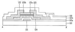
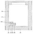
도 5는 본 발명의 실시예에 따른 산화물 박막 트랜지스터의 구조를 개략적으로 나타내는 단면도로써, 상기 도 4에 도시된 어레이 기판의 A-A'선에 따른 일부 단면을 나타내고 있다.FIG. 5 is a cross-sectional view schematically illustrating a structure of an oxide thin film transistor according to an exemplary embodiment of the present invention, and illustrates a partial cross section taken along line AA ′ of the array substrate illustrated in FIG. 4.
이때, 상기 도 5는 AxByCzO (A, B, C = Zn, Cd, Ga, In, Sn, Hf, Zr; x, y, z ≥ 0)의 조합으로 이루어진 삼성분계 또는 사성분계 산화물 반도체를 액티브층으로 사용한 산화물 박막 트랜지스터의 구조를 개략적으로 나타내고 있다.At this time, FIG. 5 is an active layer of a ternary or tetracomponent oxide semiconductor composed of a combination of AxByCzO (A, B, C = Zn, Cd, Ga, In, Sn, Hf, Zr; x, y, z ≥ 0). The structure of the oxide thin film transistor used is schematically shown.
도면에 도시된 바와 같이, 본 발명의 실시예에 따른 어레이 기판(110)에는 상기 어레이 기판(110) 위에 종횡으로 배열되어 화소영역을 정의하는 게이트라인(116)과 데이터라인(117)이 형성되어 있다. 또한, 상기 게이트라인(116)과 데이터라인(117)의 교차영역에는 스위칭소자인 박막 트랜지스터가 형성되어 있으며, 상기 화소영역 내에는 상기 박막 트랜지스터에 연결되어 컬러필터 기판(미도시)의 공통전극과 함께 액정층(미도시)을 구동시키는 화소전극(118)이 형성되어 있다.As shown in the figure, a
이때, 상기 본 발명의 실시예에 따른 산화물 박막 트랜지스터는 상기 어레이 기판(110) 위에 형성된 게이트전극(121), 상기 게이트전극(121) 위에 형성된 게이트절연막(115a), 상기 게이트전극(121) 상부에 산화물 반도체로 형성된 액티브층(124)과 소정의 절연물질로 형성된 제 1 에치 스타퍼(125a)와 제 2 에치 스타퍼(125b) 및 상기 액티브층(124)의 소오스/드레인영역과 전기적으로 접속하는 소오스/드레인전극(122, 123)으로 이루어져 있다.In this case, the oxide thin film transistor according to the exemplary embodiment of the present invention may include a
그리고, 상기 본 발명의 실시예에 따른 산화물 박막 트랜지스터는 상기 소오스/드레인전극(122, 123)이 형성된 어레이 기판(110) 위에 형성된 보호층(115b) 및 상기 보호층(115b)에 형성된 콘택홀(140)을 통해 상기 드레인전극(123)과 전기적으로 접속하는 화소전극(118)을 포함한다.In addition, the oxide thin film transistor according to the embodiment of the present invention may include a
이때, 상기 게이트전극(121)은 상기 게이트라인(116)에 연결되고 상기 소오스전극(122)의 일부는 일 방향으로 연장되어 데이터라인(117)에 연결되며, 전술한 바와 같이 상기 게이트라인(116)과 데이터라인(117)은 상기 어레이 기판(110) 위에 종횡으로 배열되어 화소영역을 정의하게 된다.In this case, the
여기서, 상기 본 발명의 실시예에 따른 산화물 박막 트랜지스터는 AxByCzO (A, B, C = Zn, Cd, Ga, In, Sn, Hf, Zr; x, y, z ≥ 0)의 조합으로 이루어진 삼성분계 또는 사성분계 산화물 반도체를 이용하여 액티브층(124)을 형성함에 따라 높은 이동도와 정전류 테스트 조건을 만족하는 한편 균일한 특성이 확보되어 액정표시장치와 유기전계발광 디스플레이를 포함하는 대면적 디스플레이에 적용 가능한 장점을 가지고 있다.Here, the oxide thin film transistor according to the embodiment of the present invention is a ternary system consisting of a combination of AxByCzO (A, B, C = Zn, Cd, Ga, In, Sn, Hf, Zr; x, y, z ≥ 0) Alternatively, as the
또한, 최근 투명 전자회로에 엄청난 관심과 활동이 집중되고 있는데, 상기 산화물 반도체를 액티브층(124)으로 적용한 산화물 박막 트랜지스터는 높은 이동도를 가지는 한편 저온에서 제작이 가능함에 따라 상기 투명 전자회로에 사용될 수 있는 장점이 있다.In addition, a tremendous interest and activity has recently been focused on transparent electronic circuits, and oxide thin film transistors using the oxide semiconductor as the
또한, 상기 산화물 반도체는 넓은 밴드 갭을 가질 수 있어 높은 색순도를 갖는 UV 발광 다이오드(Light Emitting Diode; LED), 백색 LED와 그밖에 다른 부품들을 제작할 수 있으며, 저온에서 공정이 가능하여 가볍고 유연한 제품을 생산할 수 있는 특징을 가지고 있다.In addition, since the oxide semiconductor may have a wide band gap, it is possible to manufacture UV light emitting diodes (LEDs), white LEDs, and other components having high color purity, and may be processed at low temperatures to produce light and flexible products. It has features that can be.
이와 같은 특징을 가진 상기 본 발명의 실시예에 따른 산화물 박막 트랜지스터는 상기 액티브층(124)의 채널영역 상부에 소정의 절연물질로 이루어진 상기 제 1 에치 스타퍼(125a)와 제 2 에치 스타퍼(125b)가 형성되어 있는데, 상기 제 1 에치 스타퍼(125a)와 제 2 에치 스타퍼(125b)는 후(後)공정의 플라즈마 처리에 의해 채널영역의 캐리어 농도가 변화하는 것을 방지하는 역할을 한다.In the oxide thin film transistor according to the embodiment of the present invention having the above characteristics, the
또한, 상기 본 발명의 실시예에 따른 산화물 박막 트랜지스터는 산화물 반도체층을 증착한 후 바로 절연층을 증착하여 상기 제 1 에치 스타퍼(125a)를 형성함으로써 공정 중에 화학물질 또는 UV에 의해 액티브층(124)의 백 채널이 손상 받는 것을 최소화할 수 있게 되다. 즉, 산화물 반도체층과 절연층을 연속으로 증착하여 액티브층(124)을 형성한 후, 다시 절연층을 증착하고 패터닝하여 제 1 에치 스타퍼(125a)와 제 2 에치 스타퍼(125b)를 형성하게 되는데, 이를 다음의 산화물 박막 트랜지스터의 제조방법을 통해 상세히 설명한다.In addition, the oxide thin film transistor according to the exemplary embodiment of the present invention forms the
이때, 도면에는 자세히 도시하지 않았지만, 상기 액티브층(124)과 제 2 에치 스타퍼(125b)는 서로 직교하는 방향으로 배열되는 한편, 상기 제 1 에치 스타퍼(125a)와 제 2 에치 스타퍼(125b)에 의해 가려지지 않고 노출되는 액티브층(124)의 좌우 영역은 상기 소오스/드레인전극(122, 123)과의 콘택영역을 형성하는 소오스/드레인영역을 이루게 된다.In this case, although not shown in detail, the
또한, 상기 제 1 에치 스타퍼(125a)와 제 2 에치 스타퍼(125b) 및 액티브층(124)은 아일랜드(island) 형태를 가지며, 상기 제 2 에치 스타퍼(125b)는 그 하부의 제 1 에치 스타퍼(125a)와 실질적으로 동일한 폭을 가지도록 패터닝되는 것을 특징으로 한다.In addition, the
도 6a 내지 도 6f는 상기 도 4에 도시된 본 발명의 실시예에 따른 어레이 기판의 제조공정을 순차적으로 나타내는 평면도이다.6A through 6F are plan views sequentially illustrating a process of manufacturing an array substrate according to an exemplary embodiment of the present invention illustrated in FIG. 4.
또한, 도 7a 내지 도 7g는 상기 도 5에 도시된 본 발명의 실시예에 따른 산화물 박막 트랜지스터의 제조공정을 순차적으로 나타내는 단면도이다.7A to 7G are cross-sectional views sequentially illustrating a manufacturing process of an oxide thin film transistor according to an exemplary embodiment of the present invention illustrated in FIG. 5.
도 6a 및 도 7a에 도시된 바와 같이, 투명한 절연물질로 이루어진 어레이 기판(110) 위에 소정의 게이트전극(121)과 게이트라인(116)을 형성한다.As shown in FIGS. 6A and 7A, a
이때, 본 발명의 산화물 박막 트랜지스터에 적용되는 산화물 반도체는 저온 증착이 가능하여, 플라스틱 기판, 소다라임 글라스 등의 저온 공정에 적용이 가능한 기판을 사용할 수 있다. 또한, 비정질 특성을 나타냄으로 인해 대면적 디스플레이용 기판의 사용이 가능하다.At this time, the oxide semiconductor applied to the oxide thin film transistor of the present invention can be a low temperature deposition, it is possible to use a substrate that can be applied to low-temperature processes such as plastic substrate, soda lime glass. In addition, because of the amorphous properties, it is possible to use a substrate for a large area display.
또한, 상기 게이트전극(121)과 게이트라인(116)은 제 1 도전막을 상기 어레이 기판(110) 전면에 증착한 후 포토공정을 통해 선택적으로 패터닝하여 형성하게 된다.In addition, the
여기서, 상기 제 1 도전막으로 알루미늄(aluminium; Al), 알루미늄 합금(Al alloy), 텅스텐(tungsten; W), 구리(copper; Cu), 니켈(nickel; Ni), 크롬(chromium; Cr), 몰리브덴(molybdenum; Mo), 몰리브덴 합금(Mo alloy), 티타늄(titanium; Ti), 백금(platinum; Pt), 탄탈(tantalum; Ta) 등과 같은 저저항 불투명 도전물질을 사용할 수 있다. 또한, 상기 제 1 도전막은 인듐-틴-옥사이드(Indium Tin Oxide; ITO), 인듐-징크-옥사이드(Indium Zinc Oxide; IZO)와 같은 투명한 도전물질을 사용할 수 있으며, 상기 도전물질이 2가지 이상 적층된 다층구조로 형성할 수 있다.The first conductive layer may include aluminum (Al), aluminum alloy (Al alloy), tungsten (W), copper (Cu), nickel (Ni), chromium (Cr), Low resistance opaque conductive materials such as molybdenum (Mo), molybdenum alloy (Mo alloy), titanium (Ti), platinum (Pt), tantalum (Ta), and the like may be used. In addition, the first conductive layer may be a transparent conductive material such as indium tin oxide (ITO) or indium zinc oxide (IZO), and the conductive material may be stacked in two or more kinds. It can be formed in a multi-layered structure.
다음으로, 도 7b에 도시된 바와 같이, 상기 게이트전극(121)과 게이트라인(116)이 형성된 어레이 기판(110) 전면에 차례대로 게이트절연막(115a)과 소정의 산화물 반도체로 이루어진 산화물 반도체층(120) 및 소정의 절연물질로 이루어진 제 1 절연층(125)을 형성한다.Next, as illustrated in FIG. 7B, an oxide semiconductor layer including a
이때, 상기 게이트절연막(115a)으로 실리콘질화막(SiNx), 실리콘산화막(SiO2)과 같은 무기절연막 또는 하프늄(hafnium; Hf) 옥사이드, 알루미늄 옥사이드와 같은 고유전성 산화막을 사용할 수 있으며, 상기 제 1 절연층(125)으로 실리콘산화막을 사용할 수 있다.In this case, an inorganic insulating film such as silicon nitride film (SiNx) or silicon oxide film (SiO2 ), or a high dielectric oxide film such as hafnium (Hf) oxide or aluminum oxide may be used as the
또한, 상기 산화물 반도체층(120)은 예를 들어 AxByCzO (A, B, C = Zn, Cd, Ga, In, Sn, Hf, Zr; x, y, z ≥ 0)의 조합으로 이루어진 삼성분계 또는 사성분계 산화물 반도체로 형성할 수 있다.In addition, the
그리고, 상기 게이트절연막(115a) 및 제 절연층(125)은 플라즈마 화학기상증착(Plasma Enhanced Chemical Vapour Deposition; PECVD)과 같은 화학기상증착방식으로 형성할 수 있으며, 스퍼터링(sputtering)과 같은 물리기상증착(Physical Vapour Deposition; PVD)방식으로 형성할 수도 있다.In addition, the
다음으로, 도 6b 및 도 7c에 도시된 바와 같이, 포토공정을 통해 상기 제 1 절연층과 산화물 반도체층을 선택적으로 패터닝하게 되면, 상기 어레이 기판(110)의 게이트전극(121) 상부에 상기 산화물 반도체로 이루어진 액티브층(124)이 형성되게 된다.Next, as shown in FIGS. 6B and 7C, when the first insulating layer and the oxide semiconductor layer are selectively patterned through a photo process, the oxide is disposed on the
이때, 상기 액티브층(124) 위에는 상기 절연물질로 이루어지며 상기 액티브층(124)과 실질적으로 동일한 형태로 패터닝된 절연층패턴(125')이 형성되게 된다.In this case, an insulating
이때, 상기 제 1 절연층의 식각에는 산소 플라즈마 처리와 같은 건식각을 이용할 수 있으며, 상기 절연층패턴(125')은 그 하부의 액티브층(124)과 실질적으로 동일한 형태로 패터닝됨에 따라 상기 제 1 절연층이 식각되는 동안 그 하부의 산화물 반도체층, 즉 상기 액티브층(124)의 전 영역은 노출이 완전하게 방지되어 노출에 의한 불안정성이 제거되는 동시에 상기 절연층패턴(125')의 패터닝에 의한 손상을 방지할 수 있게 된다.In this case, dry etching, such as an oxygen plasma treatment, may be used for etching the first insulating layer, and the insulating
다음으로, 도 6c 및 도 7d에 도시된 바와 같이, 상기 액티브층(124)과 절연층패턴이 형성된 어레이 기판(110) 전면에 소정의 절연물질로 이루어진 제 2 절연층을 증착한 후, 포토공정을 통해 상기 절연층패턴과 제 2 절연층을 선택적으로 패터닝하게 되면, 상기 액티브층(124)의 좌우 영역, 즉 소오스/드레인영역을 제외한 액티브층(124) 상부에 상기 절연물질로 이루어진 제 1 에치 스타퍼(125a)와 제 2 에치 스타퍼(125b)가 차례대로 형성되게 된다.Next, as illustrated in FIGS. 6C and 7D, a second insulating layer made of a predetermined insulating material is deposited on the entire surface of the
이때, 상기 제 2 절연층으로 실리콘질화막, 실리콘산화막과 같은 무기절연막 또는 하프늄 옥사이드, 알루미늄 옥사이드와 같은 고유전성 산화막을 사용할 수 있다.In this case, an inorganic insulating layer such as a silicon nitride film or a silicon oxide film or a high dielectric oxide film such as hafnium oxide or aluminum oxide may be used as the second insulating layer.
여기서, 상기 액티브층(124)과 제 2 에치 스타퍼(125b)는 서로 직교하는 방향으로 배열되는 한편, 상기 제 1 에치 스타퍼(125a)와 제 2 에치 스타퍼(125b) 및 액티브층(124)은 아일랜드 형태를 가지며, 상기 제 2 에치 스타퍼(125b)는 그 하부의 제 1 에치 스타퍼(125a)와 실질적으로 동일한 폭을 가지도록 패터닝되게 된다.Here, the
또한, 상기 제 1 에치 스타퍼(125a)와 제 2 에치 스타퍼(125b)에 의해 가려지지 않고 노출되는 액티브층(124)의 소오스/드레인영역은 상기 제 1 에치 스타퍼(125a)와 제 2 에치 스타퍼(125b)를 형성하기 위해 산소 플라즈마 처리를 통해 상기 절연층패턴과 제 2 절연층을 식각할 때 상기 산소 플라즈마에 의해 저항이 감소됨에 따라 후술할 소오스/드레인전극과의 콘택영역을 형성하게 된다. 다만, 본 발명이 이에 한정되는 것은 아니며, 상기 제 1 에치 스타퍼(125a)와 제 2 에치 스타퍼(125b)를 형성한 후 산소 플라즈마와 같은 표면처리 또는 열처리를 통해 노출된 액티브층(124)의 저항을 감소시켜 콘택영역인 소오스/드레인영역을 형성할 수도 있다.In addition, the source / drain regions of the
그리고, 본 발명의 실시예에 따른 상기 액티브층(124)은 게이트전극(121)과 직교하는 방향으로 배열되는 경우를 예를 들어 설명하고 있으나, 본 발명이 이에 한정되는 것은 아니며, 상기 액티브층(124)은 상기 게이트전극(121)과 동일한 방향으로 배열되도록 패터닝할 수도 있으며, 이 경우 상기 제 2 에치 스타퍼(125b)는 그 하부의 액티브층(124)과 직교하는 방향, 즉 상기 게이트전극(121)과 직교하는 방향으로 배열되도록 패터닝하게 된다.In addition, the
이와 같이 본 발명의 실시예의 경우에는 게이트절연막(115a)과 산화물 반도체층 및 제 1 절연층을 연속 증착하여 액티브층(124)을 형성한 후, 다시 제 2 절연층을 증착하고 패터닝하여 제 1 에치 스타퍼(125a)와 제 2 에치 스타퍼(125b)를 형성함으로써 액티브층(124)의 백 채널영역의 노출을 완전히 방지하는 한편, 노출에 의한 불안정성을 제거하는 동시에 게이트절연막(115a)의 손실을 방지할 수 있게 된다.As described above, in the exemplary embodiment of the present invention, the
다음으로, 도 6d 및 도 7e에 도시된 바와 같이, 상기 액티브층(124)과 제 1 에치 스타퍼(125a) 및 제 2 에치 스타퍼(125b)가 형성된 어레이 기판(110) 전면에 제 2 도전막을 형성한다.Next, as illustrated in FIGS. 6D and 7E, a second conductive layer is formed on the entire surface of the
이때, 상기 제 2 도전막은 소오스전극과 드레인전극 및 데이터라인을 형성하기 위해 알루미늄, 알루미늄 합금, 텅스텐, 구리, 니켈, 크롬, 몰리브덴, 몰리브덴 합금, 티타늄, 백금, 탄탈 등과 같은 저저항 불투명 도전물질을 사용할 수 있다. 또한, 상기 제 2 도전막은 인듐-틴-옥사이드, 인듐-징크-옥사이드와 같은 투명한 도전물질을 사용할 수 있으며, 상기 도전물질이 2가지 이상 적층된 다층구조로 형성할 수 있다.In this case, the second conductive layer may be formed of a low resistance opaque conductive material such as aluminum, aluminum alloy, tungsten, copper, nickel, chromium, molybdenum, molybdenum alloy, titanium, platinum, tantalum, or the like to form a source electrode, a drain electrode, and a data line. Can be used. In addition, the second conductive layer may use a transparent conductive material such as indium tin oxide or indium zinc oxide, and may have a multilayer structure in which two or more conductive materials are stacked.
그리고, 포토공정을 통해 상기 제 2 도전막을 선택적으로 패터닝함으로써 상기 액티브층(124)의 소오스영역 및 드레인영역과 각각 전기적으로 접속하는 소오스전극(122) 및 드레인전극(123)을 형성하게 된다.The second conductive film is selectively patterned through a photo process to form source and drain
다음으로, 도 6e 및 도 7f에 도시된 바와 같이, 상기 소오스/드레인전극(122, 123)이 형성된 어레이 기판(110) 전면에 보호막(115b)을 형성한 후, 포토공정을 통해 선택적으로 제거함으로써 상기 어레이 기판(110)에 상기 드레인전극(123)의 일부를 노출시키는 콘택홀(140)을 형성한다.Next, as shown in FIGS. 6E and 7F, the
그리고, 도 6f 및 도 7g에 도시된 바와 같이, 상기 보호막(115b)이 형성된 어레이 기판(110) 전면에 제 3 도전막을 형성한 후, 포토공정을 통해 선택적으로 제거함으로써 상기 어레이 기판(110)에 상기 제 3 도전막으로 이루어지며, 상기 콘택홀(140)을 통해 드레인전극(123)과 전기적으로 접속하는 화소전극(118)을 형성한다.6F and 7G, after forming a third conductive film on the entire surface of the
이때, 상기 제 3 도전막은 상기 화소전극(118)을 구성하기 위해 인듐-틴-옥사이드 또는 인듐-징크-옥사이드와 같은 투과율이 뛰어난 투명한 도전물질을 포함한다.In this case, the third conductive layer includes a transparent conductive material having excellent transmittance such as indium tin oxide or indium zinc oxide to form the
한편, 도 8 및 도 9는 산화물 박막 트랜지스터의 트랜스퍼(transfer) 특성을 나타내는 그래프로써, 상기 도 8은 일반적인 산화물 박막 트랜지스터의 트랜스퍼 특성을 나타내고, 상기 도 9는 본 발명의 실시예에 따른 산화물 박막 트랜지스터의 트랜스퍼 특성을 나타내고 있다.8 and 9 are graphs showing transfer characteristics of an oxide thin film transistor, and FIG. 8 shows transfer characteristics of a general oxide thin film transistor, and FIG. 9 is an oxide thin film transistor according to an embodiment of the present invention. The transfer characteristics of are shown.
이때, 상기 도 8 및 도 9는 초기 상태(INI)와 스트레스(stress)를 가한 상태(FIN)에 있어 각각의 산화물 박막 트랜지스터에 대한 트랜스퍼 특성을 측정한 결과를 나타내고 있다.8 and 9 illustrate results of measuring transfer characteristics of the oxide thin film transistors in the initial state INI and the stress FIN.
예를 들어, 상기 스트레스 테스트는 게이트전압에 -30V의 네거티브 바이어스를 가하는 것으로, 60℃의 온도 및 5,000nit의 백라이트 조사 하에서 1시간 동안 네거티브 바이어스를 가하게 된다.For example, the stress test is to apply a negative bias of -30V to the gate voltage, a negative bias for 1 hour under a temperature of 60 ℃ and a backlight of 5,000 nit.
도면에 도시된 바와 같이, 일반적인 산화물 박막 트랜지스터는 본 발명의 실시예에 따른 산화물 박막 트랜지스터에 비해 트랜스퍼 곡선의 기울기(slop)가 보다 완만하고 온 전류(on current)도 낮은 한편, 스트레스 테스트에 의해 소자 특성이 저하되는 것을 알 수 있는데, 이는 액티브층과 에치 스타퍼를 형성하기 위한 포토공정에 의해 액티브층의 백 채널영역이 어느 정도 손상을 받았기 때문이다.As shown in the figure, a typical oxide thin film transistor has a more gentle slop of the transfer curve and a lower on current than the oxide thin film transistor according to the embodiment of the present invention, It can be seen that the characteristics are deteriorated because the back channel region of the active layer is damaged to some extent by the photo process for forming the active layer and the etch stopper.
이에 비해 본 발명의 실시예에 따른 산화물 박막 트랜지스터는 트랜스퍼 곡선의 기울기가 급하고 온 전류도 향상되어 트랜스퍼 특성이 향상되었음을 알 수 있으며, 스트레스 테스트에 의한 소자 특성의 저하가 일어나지 않음을 알 수 있다.On the other hand, the oxide thin film transistor according to the embodiment of the present invention shows that the slope of the transfer curve is steep and the on-current is also improved, and thus the transfer characteristics are improved, and the deterioration of the device characteristics due to the stress test does not occur.
전술한 바와 같이 본 발명은 액정표시장치뿐만 아니라 박막 트랜지스터를 이용하여 제작하는 다른 표시장치, 예를 들면 구동 트랜지스터에 유기전계발광소자가 연결된 유기전계발광 디스플레이장치에도 이용될 수 있다.As described above, the present invention can be used not only in a liquid crystal display device but also in another display device manufactured using a thin film transistor, for example, an organic light emitting display device in which an organic light emitting element is connected to a driving transistor.
또한, 본 발명은 높은 이동도를 가지는 한편 저온에서 공정이 가능한 비정질 산화물 반도체 물질을 액티브층으로 적용함에 따라 투명 전자회로나 플렉서블(flexible) 디스플레이에 사용될 수 있는 장점이 있다.In addition, the present invention has an advantage that it can be used in a transparent electronic circuit or a flexible display by applying an amorphous oxide semiconductor material capable of processing at low temperature while having high mobility as an active layer.
상기한 설명에 많은 사항이 구체적으로 기재되어 있으나 이것은 발명의 범위를 한정하는 것이라기보다 바람직한 실시예의 예시로서 해석되어야 한다. 따라서 발명은 설명된 실시예에 의하여 정할 것이 아니고 특허청구범위와 특허청구범위에 균등한 것에 의하여 정하여져야 한다.Many details are set forth in the foregoing description but should be construed as illustrative of preferred embodiments rather than to limit the scope of the invention. Therefore, the invention should not be defined by the described embodiments, but should be defined by the claims and their equivalents.
110 : 어레이 기판118 : 화소전극
121 : 게이트전극122 : 소오스전극
123 : 드레인전극124 : 액티브층
125a,125b : 에치 스타퍼110: array substrate 118: pixel electrode
121: gate electrode 122: source electrode
123: drain electrode 124: active layer
125a, 125b: etch stopper
Claims (11)
Translated fromKorean상기 기판 위에 연속하여 게이트절연막, 산화물 반도체층 및 제 1 절연층을 형성하는 단계;
상기 산화물 반도체층과 제 1 절연층을 선택적으로 패터닝하여 상기 게이트전극 상부에 액티브층과 절연층패턴을 형성하는 단계;
상기 액티브층과 절연층패턴이 형성된 기판 위에 제 2 절연층을 형성하는 단계;
상기 절연층패턴과 제 2 절연층을 선택적으로 패터닝하여 상기 액티브층 위에 제 1 에치 스타퍼와 제 2 에치 스타퍼를 형성하는 단계; 및
상기 제 1 에치 스타퍼와 제 2 에치 스타퍼가 형성된 기판 위에 상기 액티브층의 소오스/드레인영역과 전기적으로 접속하는 소오스/드레인전극을 형성하는 단계를 포함하며, 상기 산화물 반도체층은 AxByCzO (A, B, C = Zn, Cd, Ga, In, Sn, Hf, Zr; x, y, z ≥ 0)의 조합으로 이루어진 삼성분계 또는 사성분계 산화물 반도체로 이루어진 것을 특징으로 하는 산화물 박막 트랜지스터의 제조방법.Forming a gate electrode on the substrate;
Continuously forming a gate insulating film, an oxide semiconductor layer, and a first insulating layer on the substrate;
Selectively patterning the oxide semiconductor layer and the first insulating layer to form an active layer and an insulating layer pattern on the gate electrode;
Forming a second insulating layer on the substrate on which the active layer and the insulating layer pattern are formed;
Selectively patterning the insulating layer pattern and the second insulating layer to form a first etch stopper and a second etch stopper on the active layer; And
And forming a source / drain electrode electrically connected to the source / drain regions of the active layer on the substrate on which the first etch stopper and the second etch stopper are formed, wherein the oxide semiconductor layer comprises AxByCzO (A, B, C = Zn, Cd, Ga, In, Sn, Hf, Zr; x, y, z ≥ 0) method of manufacturing an oxide thin film transistor, characterized in that consisting of a quarter- or quad-component oxide semiconductor.
Priority Applications (3)
| Application Number | Priority Date | Filing Date | Title |
|---|---|---|---|
| KR1020100127171AKR20120065854A (en) | 2010-12-13 | 2010-12-13 | Method of fabricating oxide thin film transistor |
| CN2011104625450ACN102543754A (en) | 2010-12-13 | 2011-12-12 | Oxide thin film transistor and method of fabricating the same |
| US13/324,751US8735883B2 (en) | 2010-12-13 | 2011-12-13 | Oxide thin film transistor and method of fabricating the same |
Applications Claiming Priority (1)
| Application Number | Priority Date | Filing Date | Title |
|---|---|---|---|
| KR1020100127171AKR20120065854A (en) | 2010-12-13 | 2010-12-13 | Method of fabricating oxide thin film transistor |
Publications (1)
| Publication Number | Publication Date |
|---|---|
| KR20120065854Atrue KR20120065854A (en) | 2012-06-21 |
Family
ID=46198420
Family Applications (1)
| Application Number | Title | Priority Date | Filing Date |
|---|---|---|---|
| KR1020100127171AWithdrawnKR20120065854A (en) | 2010-12-13 | 2010-12-13 | Method of fabricating oxide thin film transistor |
Country Status (3)
| Country | Link |
|---|---|
| US (1) | US8735883B2 (en) |
| KR (1) | KR20120065854A (en) |
| CN (1) | CN102543754A (en) |
Cited By (1)
| Publication number | Priority date | Publication date | Assignee | Title |
|---|---|---|---|---|
| KR20140129618A (en)* | 2013-04-30 | 2014-11-07 | 엘지디스플레이 주식회사 | Oxide thin film transistor and method for fabricating the same |
Families Citing this family (14)
| Publication number | Priority date | Publication date | Assignee | Title |
|---|---|---|---|---|
| TWI613822B (en) | 2011-09-29 | 2018-02-01 | 半導體能源研究所股份有限公司 | Semiconductor device and method of manufacturing same |
| KR20130136063A (en) | 2012-06-04 | 2013-12-12 | 삼성디스플레이 주식회사 | Thin film transistor, thin film transistor array panel including the same and manufacturing method thereof |
| CN103178021B (en)* | 2013-02-28 | 2015-02-11 | 京东方科技集团股份有限公司 | Oxide thin-film transistor array substrate, manufacturing method for same and display panel |
| KR102148957B1 (en) | 2013-09-02 | 2020-08-31 | 삼성디스플레이 주식회사 | Display substrate and method of manufacturing a display substrate |
| TW201515234A (en)* | 2013-10-11 | 2015-04-16 | E Ink Holdings Inc | Active device and manufacturing method thereof |
| KR102230301B1 (en) | 2014-01-06 | 2021-03-22 | 삼성디스플레이 주식회사 | Thin film transistor and manufacturing method thereof |
| CN103915379B (en)* | 2014-03-24 | 2017-07-04 | 京东方科技集团股份有限公司 | A kind of manufacture method of oxide film transistor array substrate |
| TWI563669B (en)* | 2014-08-04 | 2016-12-21 | Innolux Corp | Thin film transistor and display panel using the same |
| CN104347643B (en)* | 2014-09-04 | 2017-07-28 | 上海天马微电子有限公司 | Driving circuit and forming method thereof, organic light emitting display device and forming method thereof |
| CN105914150A (en)* | 2016-04-29 | 2016-08-31 | 京东方科技集团股份有限公司 | Film transistor and the manufacturing method thereof, array substrate and the manufacturing method of, display panel and display apparatus |
| CN109244085A (en)* | 2018-09-27 | 2019-01-18 | 惠科股份有限公司 | Array substrate and display panel |
| CN113345924B (en)* | 2021-06-03 | 2024-06-11 | 京东方科技集团股份有限公司 | Display panel, manufacturing method thereof, and display device |
| CN114373682A (en)* | 2022-01-06 | 2022-04-19 | 上海大学 | A kind of preparation method of back channel etched structure oxide thin film transistor |
| CN114709173A (en)* | 2022-03-30 | 2022-07-05 | 广州华星光电半导体显示技术有限公司 | Array substrate, preparation method thereof and display panel |
Family Cites Families (4)
| Publication number | Priority date | Publication date | Assignee | Title |
|---|---|---|---|---|
| JP3880568B2 (en)* | 2002-10-25 | 2007-02-14 | 鹿児島日本電気株式会社 | Manufacturing method of liquid crystal display device |
| JP5704790B2 (en)* | 2008-05-07 | 2015-04-22 | キヤノン株式会社 | Thin film transistor and display device |
| KR101496148B1 (en)* | 2008-05-15 | 2015-02-27 | 삼성전자주식회사 | Semiconductor device and manufacturing method thereof |
| JP2010182819A (en) | 2009-02-04 | 2010-08-19 | Sony Corp | Thin-film transistor, and display device |
- 2010
- 2010-12-13KRKR1020100127171Apatent/KR20120065854A/ennot_activeWithdrawn
- 2011
- 2011-12-12CNCN2011104625450Apatent/CN102543754A/enactivePending
- 2011-12-13USUS13/324,751patent/US8735883B2/enactiveActive
Cited By (1)
| Publication number | Priority date | Publication date | Assignee | Title |
|---|---|---|---|---|
| KR20140129618A (en)* | 2013-04-30 | 2014-11-07 | 엘지디스플레이 주식회사 | Oxide thin film transistor and method for fabricating the same |
Also Published As
| Publication number | Publication date |
|---|---|
| US8735883B2 (en) | 2014-05-27 |
| CN102543754A (en) | 2012-07-04 |
| US20120146017A1 (en) | 2012-06-14 |
Similar Documents
| Publication | Publication Date | Title |
|---|---|---|
| KR101218090B1 (en) | Oxide thin film transistor and method of fabricating the same | |
| US8735883B2 (en) | Oxide thin film transistor and method of fabricating the same | |
| KR101578694B1 (en) | Manufacturing method of oxide thin film transistor | |
| JP5129228B2 (en) | Array substrate and manufacturing method thereof | |
| JP6262276B2 (en) | Oxide thin film transistor and method for manufacturing the same | |
| KR101593443B1 (en) | Method of fabricating array substrate | |
| KR101019048B1 (en) | Array substrate and its manufacturing method | |
| KR101658533B1 (en) | Oxide thin film transistor and method of fabricating the same | |
| KR20110125105A (en) | Oxide thin film transistor and its manufacturing method | |
| KR20120136695A (en) | Oxide thin film transistor and method of fabricating the same | |
| KR101622733B1 (en) | Method of fabricating oxide thin film transistor | |
| KR101697586B1 (en) | Oxide thin film transistor and method of fabricating the same | |
| KR20100002899A (en) | Method of fabricating oxide thin film transistor | |
| KR101605723B1 (en) | Method of fabricating oxide thin film transistor | |
| KR101375854B1 (en) | Oxide thin film transistor and method of fabricating the same | |
| KR102039424B1 (en) | Method of fabricating oxide thin film transistor | |
| KR101545923B1 (en) | Oxide thin film transistor and method of fabricating the same | |
| KR101640812B1 (en) | Method of fabricating oxide thin film transistor | |
| KR101298611B1 (en) | Oxide thin film transistor and method of fabricating the same | |
| KR20110055274A (en) | Method of manufacturing oxide thin film transistor | |
| KR101375853B1 (en) | Oxide thin film transistor and method of fabricating the same | |
| KR101875940B1 (en) | Oxide thin film transistor and method for fabricating the same | |
| KR20110027470A (en) | Method of manufacturing oxide thin film transistor | |
| KR20120075110A (en) | Method of fabricating oxide thin film transistor | |
| KR20110073038A (en) | Oxide thin film transistor and its manufacturing method |
Legal Events
| Date | Code | Title | Description |
|---|---|---|---|
| PA0109 | Patent application | Patent event code:PA01091R01D Comment text:Patent Application Patent event date:20101213 | |
| PG1501 | Laying open of application | ||
| PC1203 | Withdrawal of no request for examination | ||
| WITN | Application deemed withdrawn, e.g. because no request for examination was filed or no examination fee was paid |