KR20120050282A - Light emitting device package and method of manufacturing the same - Google Patents
Light emitting device package and method of manufacturing the sameDownload PDFInfo
- Publication number
- KR20120050282A KR20120050282AKR1020100111706AKR20100111706AKR20120050282AKR 20120050282 AKR20120050282 AKR 20120050282AKR 1020100111706 AKR1020100111706 AKR 1020100111706AKR 20100111706 AKR20100111706 AKR 20100111706AKR 20120050282 AKR20120050282 AKR 20120050282A
- Authority
- KR
- South Korea
- Prior art keywords
- light emitting
- emitting device
- device package
- reflective wall
- electrodes
- Prior art date
- Legal status (The legal status is an assumption and is not a legal conclusion. Google has not performed a legal analysis and makes no representation as to the accuracy of the status listed.)
- Ceased
Links
Images


Classifications
- H—ELECTRICITY
- H10—SEMICONDUCTOR DEVICES; ELECTRIC SOLID-STATE DEVICES NOT OTHERWISE PROVIDED FOR
- H10H—INORGANIC LIGHT-EMITTING SEMICONDUCTOR DEVICES HAVING POTENTIAL BARRIERS
- H10H20/00—Individual inorganic light-emitting semiconductor devices having potential barriers, e.g. light-emitting diodes [LED]
- H10H20/80—Constructional details
- H10H20/85—Packages
- H10H20/851—Wavelength conversion means
- H10H20/8514—Wavelength conversion means characterised by their shape, e.g. plate or foil
- H—ELECTRICITY
- H10—SEMICONDUCTOR DEVICES; ELECTRIC SOLID-STATE DEVICES NOT OTHERWISE PROVIDED FOR
- H10H—INORGANIC LIGHT-EMITTING SEMICONDUCTOR DEVICES HAVING POTENTIAL BARRIERS
- H10H20/00—Individual inorganic light-emitting semiconductor devices having potential barriers, e.g. light-emitting diodes [LED]
- H10H20/01—Manufacture or treatment
- H10H20/036—Manufacture or treatment of packages
- H—ELECTRICITY
- H10—SEMICONDUCTOR DEVICES; ELECTRIC SOLID-STATE DEVICES NOT OTHERWISE PROVIDED FOR
- H10H—INORGANIC LIGHT-EMITTING SEMICONDUCTOR DEVICES HAVING POTENTIAL BARRIERS
- H10H20/00—Individual inorganic light-emitting semiconductor devices having potential barriers, e.g. light-emitting diodes [LED]
- H10H20/80—Constructional details
- H10H20/85—Packages
- H10H20/8506—Containers
- H—ELECTRICITY
- H10—SEMICONDUCTOR DEVICES; ELECTRIC SOLID-STATE DEVICES NOT OTHERWISE PROVIDED FOR
- H10H—INORGANIC LIGHT-EMITTING SEMICONDUCTOR DEVICES HAVING POTENTIAL BARRIERS
- H10H20/00—Individual inorganic light-emitting semiconductor devices having potential barriers, e.g. light-emitting diodes [LED]
- H10H20/80—Constructional details
- H10H20/85—Packages
- H10H20/851—Wavelength conversion means
- H10H20/8515—Wavelength conversion means not being in contact with the bodies
- H—ELECTRICITY
- H10—SEMICONDUCTOR DEVICES; ELECTRIC SOLID-STATE DEVICES NOT OTHERWISE PROVIDED FOR
- H10H—INORGANIC LIGHT-EMITTING SEMICONDUCTOR DEVICES HAVING POTENTIAL BARRIERS
- H10H20/00—Individual inorganic light-emitting semiconductor devices having potential barriers, e.g. light-emitting diodes [LED]
- H10H20/80—Constructional details
- H10H20/85—Packages
- H10H20/855—Optical field-shaping means, e.g. lenses
- H10H20/856—Reflecting means
- H—ELECTRICITY
- H10—SEMICONDUCTOR DEVICES; ELECTRIC SOLID-STATE DEVICES NOT OTHERWISE PROVIDED FOR
- H10H—INORGANIC LIGHT-EMITTING SEMICONDUCTOR DEVICES HAVING POTENTIAL BARRIERS
- H10H20/00—Individual inorganic light-emitting semiconductor devices having potential barriers, e.g. light-emitting diodes [LED]
- H10H20/80—Constructional details
- H10H20/85—Packages
- H10H20/857—Interconnections, e.g. lead-frames, bond wires or solder balls
- H—ELECTRICITY
- H01—ELECTRIC ELEMENTS
- H01L—SEMICONDUCTOR DEVICES NOT COVERED BY CLASS H10
- H01L2224/00—Indexing scheme for arrangements for connecting or disconnecting semiconductor or solid-state bodies and methods related thereto as covered by H01L24/00
- H01L2224/01—Means for bonding being attached to, or being formed on, the surface to be connected, e.g. chip-to-package, die-attach, "first-level" interconnects; Manufacturing methods related thereto
- H01L2224/42—Wire connectors; Manufacturing methods related thereto
- H01L2224/47—Structure, shape, material or disposition of the wire connectors after the connecting process
- H01L2224/48—Structure, shape, material or disposition of the wire connectors after the connecting process of an individual wire connector
- H01L2224/4805—Shape
- H01L2224/4809—Loop shape
- H01L2224/48091—Arched
- H—ELECTRICITY
- H01—ELECTRIC ELEMENTS
- H01L—SEMICONDUCTOR DEVICES NOT COVERED BY CLASS H10
- H01L2224/00—Indexing scheme for arrangements for connecting or disconnecting semiconductor or solid-state bodies and methods related thereto as covered by H01L24/00
- H01L2224/01—Means for bonding being attached to, or being formed on, the surface to be connected, e.g. chip-to-package, die-attach, "first-level" interconnects; Manufacturing methods related thereto
- H01L2224/42—Wire connectors; Manufacturing methods related thereto
- H01L2224/47—Structure, shape, material or disposition of the wire connectors after the connecting process
- H01L2224/48—Structure, shape, material or disposition of the wire connectors after the connecting process of an individual wire connector
- H01L2224/481—Disposition
- H01L2224/48151—Connecting between a semiconductor or solid-state body and an item not being a semiconductor or solid-state body, e.g. chip-to-substrate, chip-to-passive
- H01L2224/48221—Connecting between a semiconductor or solid-state body and an item not being a semiconductor or solid-state body, e.g. chip-to-substrate, chip-to-passive the body and the item being stacked
- H01L2224/48245—Connecting between a semiconductor or solid-state body and an item not being a semiconductor or solid-state body, e.g. chip-to-substrate, chip-to-passive the body and the item being stacked the item being metallic
- H01L2224/48247—Connecting between a semiconductor or solid-state body and an item not being a semiconductor or solid-state body, e.g. chip-to-substrate, chip-to-passive the body and the item being stacked the item being metallic connecting the wire to a bond pad of the item
Landscapes
- Led Device Packages (AREA)
Abstract
Translated fromKoreanDescription
Translated fromKorean본 발명은 발광 소자 패키지 및 그 제조 방법에 관한 것이다.The present invention relates to a light emitting device package and a method of manufacturing the same.
광원의 일종인 발광 다이오드(LED)는 전류가 가해지면 p, n형 의 접합 부분에서 전자와 정공의 재결합에 기하여, 다양한 색상의 빛을 발생시킬 수 있는 장치이다. A light emitting diode (LED), which is a kind of light source, is a device that can generate light of various colors based on the recombination of electrons and holes at p- and n-type junctions when a current is applied.
보편적인 발광 소자 패키지 제조방법은 패키지 본체에 발광 다이오드 소자를 실장하고, 발광 다이오드 소자 표면과 패키지 본체 사이의 공간에 형광체를 분산시킨 몰딩 수지로 채워 넣고 이를 경화시키는 것이다.A common method of manufacturing a light emitting device package is to mount a light emitting diode device on a package body, and to fill with a molding resin in which phosphors are dispersed in a space between the surface of the light emitting diode device and the package body and to cure it.
그러나, 종래의 몰딩 수지를 사용하는 발광 소자 패키지는 측면으로 방출된 빛이 형광체와 많은 반응을 하게 되어 적색 및 녹황색 빛이 많아지게 되고, 따라서, 이러한 흡수 및 방출 현상에 의해서 방출 방향에 따라 원하지 않는 파장대의 빛이 생성되어 방출되는 현상이 나타나게 된다. 또한 각 발광 다이오드 패키지 각각에 몰딩 수지를 주입하는 공정이 필요하므로, 생산시간이 증가하게 되며, 몰딩 수지 내부에 분산된 형광체의 침전 및, 열 경화 공정 중 열의 분포에 따라 형광체의 분산 정도가 달라짐으로 인하여 제품의 품질이 낮아지는 문제점이 있다.However, in the light emitting device package using the conventional molding resin, the light emitted from the side reacts with the phosphors a lot, resulting in a lot of red and greenish yellow light. Light generated in the wavelength band is emitted. In addition, since a process of injecting molding resin into each light emitting diode package is required, production time increases, and the degree of dispersing of the phosphor varies according to precipitation of phosphor dispersed in the molding resin and heat distribution during the heat curing process. There is a problem that the quality of the product is lowered.
본 발명은 목적은 색편차 특성이 개선되고 공정 단축이 가능하며, 광효율이 향상된 발광 소자 패키지 및 그 제조 방법을 제공하는 것이다.SUMMARY OF THE INVENTION An object of the present invention is to provide a light emitting device package and a method of manufacturing the same, which can improve color deviation and shorten a process and have improved light efficiency.
상기 기술적 과제를 실현하기 위해서, 본 발명의 일 측면은,In order to realize the above technical problem, an aspect of the present invention,
적어도 일부의 하면이 외부로 노출된 제1 및 제2 전극과, 상기 제1 및 제2 전극 중 적어도 하나의 상면에 배치되는 발광 소자와, 상기 제1 및 제2 전극의 상면에 배치되되 상기 발광 소자의 주변을 둘러싸 실장부를 형성하는 반사벽 및 상기 반사벽 상에 배치되어 상기 실장부의 상부를 덮는 형광 필름을 포함하며, 상기 실장부에는 공기가 충진된 것을 특징으로 하는 발광 소자 패키지를 제공한다.First and second electrodes at least partially exposed to the outside, a light emitting device disposed on an upper surface of at least one of the first and second electrodes, and an upper surface of the first and second electrodes, wherein the light emission It includes a reflective wall surrounding the periphery of the device to form a mounting portion and a fluorescent film disposed on the reflective wall to cover the upper portion of the mounting portion, the mounting portion is provided with a light emitting device package characterized in that the air is filled.
본 발명의 일 실시 예에서, 상기 제1 및 제2 전극, 상기 반사벽 및 상기 형광 필름이 적어도 일부 영역에서 서로 공면(co-plane)을 이루어 형성되는 측면을 가질 수 있다.In an embodiment of the present disclosure, the first and second electrodes, the reflective wall, and the fluorescent film may have side surfaces formed by co-planes with each other in at least some regions.
본 발명의 일 실시 예에서, 상기 발광 소자는 도전성 와이어를 통하여 상기 제1 및 제2 전극과 전기적으로 연결될 수 있다.In one embodiment of the present invention, the light emitting device may be electrically connected to the first and second electrodes through a conductive wire.
본 발명의 일 실시 예에서, 상기 발광 소자는 솔더층을 통하여 상기 제1 및 제2 전극과 전기적으로 연결될 수 있다.In one embodiment of the present invention, the light emitting device may be electrically connected to the first and second electrodes through a solder layer.
본 발명의 일 실시 예에서, 상기 발광 소자는 복수개 배치되되, 상기 제1 및 제2 전극을 통하여 서로 전기적으로 연결되고, 상기 반사벽은 상기 복수개의 발광 소자 각각을 둘러싸는 복수개의 실장부를 형성할 수 있다.In one embodiment of the present invention, a plurality of light emitting devices are disposed, and are electrically connected to each other through the first and second electrodes, and the reflective wall may form a plurality of mounting parts surrounding each of the plurality of light emitting devices. Can be.
본 발명의 일 실시 예에서, 상기 제1 및 제2 전극은 서로 거리를 두고 이격되어 사이에 공간을 형성하며 상기 공간에는 광반사물질이 형성될 수 있다.In one embodiment of the present invention, the first and second electrodes are spaced apart from each other to form a space therebetween, the light reflecting material may be formed in the space.
이 경우, 상기 광반사물질은 상기 반사벽과 동일한 소재로 이루어질 수 있다.In this case, the light reflecting material may be made of the same material as the reflective wall.
본 발명의 일 실시 예에서, 상기 형광 필름은 복수의 필름이 다층 적층되어 이루어질 수 있다.In one embodiment of the present invention, the fluorescent film may be formed by stacking a plurality of films.
본 발명의 일 실시 예에서, 상기 형광 필름은 상기 발광 소자에서 방출된 빛을 황색, 적색 및 녹색 중 적어도 하나로 파장을 변환시킬 수 있다.In one embodiment of the present invention, the fluorescent film may convert the wavelength of the light emitted from the light emitting device to at least one of yellow, red and green.
본 발명의 일 실시 예에서, 상기 형광 필름은 봉지재 및 그 내부에 혼합된 형광체를 포함하여 이루어질 수 있다.In one embodiment of the present invention, the fluorescent film may include an encapsulant and a phosphor mixed therein.
본 발명의 일 실시 예에서, 상기 반사벽은 상기 발광 소자 주변을 사각형으로 둘러쌀 수 있다.In one embodiment of the present invention, the reflective wall may surround the light emitting device in a rectangle.
본 발명의 일 실시 예에서, 상기 제1 및 제2 전극은 투광성을 갖는 물질로 이루어질 수 있다.In one embodiment of the present invention, the first and second electrodes may be made of a light transmitting material.
본 발명의 일 실시 예에서, 상기 반사벽은 실리콘에 분산제가 첨가될 수 있다.In one embodiment of the present invention, the reflecting wall may be a dispersant added to the silicon.
본 발명의 일 실시 예에서, 상기 실장부에는 공기가 충진될 수 있다.In one embodiment of the present invention, the mounting portion may be filled with air.
상기 형광 필름의 적어도 일부는 상기 발광 소자에 접착 될 수 있다.At least a portion of the fluorescent film may be attached to the light emitting device.
한편, 본 발명의 다른 측면은,On the other hand, another aspect of the present invention,
형광체가 분산된 형광필름을 준비하는 단계와, 제1 및 제2 전극을 형성하는 단계와, 상기 제1 및 제2 전극 상면의 적어도 일부 영역에 반사벽을 형성하여 상기 반사벽으로 둘러싸이며 상부가 외부로 연결된 실장부를 형성하는 단계와, 상기 실장부 내부에 발광 소자를 배치하는 단계와, 상기 반사벽 상에 실장부의 상부를 덮도록 상기 형광 필름을 접착하는 단계를 포함하는 발광 소자 패키지 제조 방법을 제공한다.Preparing a fluorescent film in which phosphors are dispersed, forming first and second electrodes, and forming a reflective wall on at least a portion of the upper surface of the first and second electrodes to surround the reflective wall, A method of manufacturing a light emitting device package comprising: forming a mounting unit connected to the outside; disposing a light emitting device inside the mounting unit; and bonding the fluorescent film to cover an upper portion of the mounting unit on the reflective wall. to provide.
본 발명의 일 실시 예에서, 상기 형광필름을 준비하는 단계는,In one embodiment of the present invention, the step of preparing the fluorescent film,
제1 및 제2 필름을 준비하는 단계와, 제1 액상 봉지재와 형광체를 혼합하여 혼합 봉지재를 준비하는 단계와, 상기 혼합 봉지재를 상기 제1 필름 상에 균일한 두께로 형성하는 단계와, 상기 제1 필름 상에 형성된 상기 혼합 봉지재 표면에 상기 제2 필름을 부착하는 단계 및 상기 제1 및 제2필름이 부착된 상기 혼합 봉지재를 냉장 또는 냉동 보관하는 단계를 포함할 수 있다.Preparing first and second films, preparing a mixed encapsulant by mixing the first liquid encapsulant and the phosphor, and forming the mixed encapsulant to a uniform thickness on the first film; The method may include attaching the second film to a surface of the mixed encapsulation material formed on the first film, and refrigerating or freezing the mixed encapsulation material having the first and second films attached thereto.
본 발명의 일 실시 예에서, 상기 반사벽 상에 상기 형광 필름을 접착하는 단계는, 상기 제1 또는 제2필름을 제거하는 단계와, 상기 혼합 봉지재를 상기 반사벽 상에 부착시키는 단계 및 상기 혼합 봉지재를 경화시켜, 상기 반사벽 상에 접착시키는 단계를 포함할 수 있다.In an embodiment of the present disclosure, the bonding of the fluorescent film on the reflective wall may include removing the first or second film, attaching the mixed encapsulant on the reflective wall, and Hardening the mixed encapsulant may include the step of adhering on the reflective wall.
본 발명의 일 실시 예에서, 상기 형광필름을 준비하는 단계는, 필름을 준비하는 단계와, 제2 액상 봉지재와 형광체를 혼합하여 혼합 봉지재를 준비하는 단계와, 상기 혼합 봉지재를 상기 필름 상에 균일한 두께로 형성하는 단계 및 상기 혼합 봉지재를 경화시키는 단계를 포함할 수 있다.In an embodiment of the present invention, the preparing of the fluorescent film may include preparing a film, mixing a second liquid encapsulant and a phosphor to prepare a mixed encapsulant, and using the mixed encapsulant as the film. Forming to a uniform thickness on the phase and may include the step of curing the mixed encapsulant.
본 발명의 일 실시 예에서, 상기 반사벽 상에 상기 형광 필름을 접착하는 단계는, 접착제를 통해 상기 경화된 혼합 봉지재를 상기 반사벽 상에 접착시킬 수 있다.In one embodiment of the present invention, the step of adhering the fluorescent film on the reflective wall, it is possible to adhere the cured mixed encapsulant on the reflective wall through an adhesive.
본 발명의 일 실시 예에서, 상기 형광필름을 준비하는 단계는, 제1 및 제2 필름을 준비하는 단계와, UV 경화제를 포함하는 봉지재와 형광체를 혼합하여 혼합 봉지재를 준비하는 단계와, 상기 혼합 봉지재를 상기 제1필름 상에 균일한 두께로 형성하는 단계와, 상기 제1필름 상에 형성된 상기 혼합 봉지재 표면에 상기 제2필름을 부착하는 단계 및 상기 제1 및 제2필름이 부착된 상기 혼합 봉지재를 냉장 또는 냉동 보관하는 단계를 포함할 수 있다.In one embodiment of the present invention, the step of preparing the fluorescent film, the step of preparing the first and second film, the step of preparing a mixed encapsulant by mixing the encapsulant and the phosphor containing a UV curing agent, Forming the mixed encapsulant to a uniform thickness on the first film, attaching the second film to a surface of the mixed encapsulant formed on the first film, and the first and second films It may include the step of refrigeration or freezing the mixed encapsulant attached.
본 발명의 일 실시 예에서, 상기 반사벽 상에 형광필름을 접착시키는 단계는, 상기 제1 또는 제2필름을 제거하는 단계와, 상기 혼합 봉지재를 상기 반사벽 상에 부착시키는 단계 및 상기 혼합 봉지재를 UV 경화를 통해, 상기 반사벽 상에 접착시키는 단계를 포함할 수 있다.In one embodiment of the present invention, the step of bonding the fluorescent film on the reflective wall, the step of removing the first or second film, the step of attaching the mixing encapsulant on the reflective wall and the mixing Bonding the encapsulant on the reflective wall through UV curing.
본 발명의 일 실시 예에서, 상기 제1 및 제2 전극과, 상기 반사벽 및 상기 형광 필름이 중첩된 영역을 두께방향으로 절단하여 적어도 하나 이상의 발광 소자 패키지를 획득하는 단계를 더 포함할 수 있다.In an embodiment of the present disclosure, the method may further include obtaining at least one light emitting device package by cutting the region in which the first and second electrodes, the reflective wall and the fluorescent film overlap, in a thickness direction. .
본 발명의 일 실시 예에서, 상기 발광 소자 패키지는, 상기 발광 소자가 복수개 배치되어 상기 제1 및 제2 전극을 통하여 서로 전기적으로 연결되고, 상기 반사벽은 상기 복수개의 발광 소자 각각을 둘러싸는 복수개의 실장부를 포함하도록 절단할 수 있다.In one embodiment of the present invention, the light emitting device package, a plurality of the light emitting device is disposed is electrically connected to each other through the first and second electrodes, the plurality of reflecting walls surround each of the plurality of light emitting devices It can be cut to include two mounting parts.
본 발명의 일 실시 예에서, 상기 실장부를 형성하는 단계는, 상기 반사벽이 상기 발광 소자 주변을 사각형으로 둘러싸도록 상기 반사벽을 형성할 수 있다.In an embodiment of the present disclosure, the forming of the mounting part may include forming the reflective wall such that the reflective wall surrounds the light emitting device in a rectangular shape.
본 발명의 일 실시 예에서, 상기 발광 소자는, 청색, 적색, 녹색 및 UV 파장을 발생시키는 발광 소자 중 적어도 하나 이상을 포함할 수 있다.In one embodiment of the present invention, the light emitting device may include at least one or more of the light emitting device for generating blue, red, green and UV wavelengths.
본 발명의 일 실시 예에서, 상기 형광체는, 황색, 적색 및 녹색 중 적어도 하나로 파장을 변환시키는 형광체로 이루어질 수 있다.In one embodiment of the present invention, the phosphor, may be made of a phosphor for converting the wavelength to at least one of yellow, red and green.
본 발명에서 제안하는 발광 소자 패키지 및 그 제조 방법을 사용하는 경우, 색편차 특성이 개선되고 공정 단축이 가능하며, 광효율이 향상되는 효과를 얻을 수 있다.In the case of using the light emitting device package and the manufacturing method proposed by the present invention, the color deviation characteristics can be improved, the process can be shortened, and the light efficiency can be obtained.
도1은 본 발명의 일 실시 형태에 따른 발광 소자 패키지를 개략적으로 나타낸 단면도이다.
도2 내지 도5는 본 발명의 일 실시 형태에 따른 발광 소자 패키지를 개략적으로 나타낸 단면도이다.
도6a 내지 도6e는, 본 발명의 일 실시 형태에 따른 발광 소자 패키지 제조방법을 나타낸 공정 단면도이다.
도7a 내지 도7c는, 본 발명의 일 실시 형태에 따른 발광 소자 패키지에서 형광필름의 제조방법을 나타낸 공정 단면도이다.1 is a cross-sectional view schematically showing a light emitting device package according to an embodiment of the present invention.
2 to 5 are cross-sectional views schematically showing a light emitting device package according to an embodiment of the present invention.
6A to 6E are cross-sectional views illustrating a method of manufacturing a light emitting device package according to an embodiment of the present invention.
7A to 7C are cross-sectional views illustrating a method of manufacturing a fluorescent film in a light emitting device package according to an embodiment of the present invention.
이하, 첨부된 도면을 참조하여 본 발명의 바람직한 실시형태들을 설명한다.Hereinafter, preferred embodiments of the present invention will be described with reference to the accompanying drawings.
그러나, 본 발명의 실시형태는 여러 가지 다른 형태로 변형될 수 있으며, 본 발명의 범위가 이하 설명하는 실시 형태로 한정되는 것은 아니다. 또한, 본 발명의 실시형태는 당해 기술 분야에서 평균적인 지식을 가진 자에게 본 발명을 더욱 완전하게 설명하기 위해서 제공되는 것이다. 따라서, 도면에서의 요소들의 형상 및 크기 등은 명확한 설명을 위해 과장될 수 있으며, 도면상의 동일한 부호로 표시되는 요소는 동일한 요소이다.
However, embodiments of the present invention may be modified in various other forms, and the scope of the present invention is not limited to the embodiments described below. Further, the embodiments of the present invention are provided to more fully explain the present invention to those skilled in the art. Accordingly, the shape and size of elements in the drawings may be exaggerated for clarity, and the elements denoted by the same reference numerals in the drawings are the same elements.
도1은 본 발명의 일 실시 형태에 따른 발광 소자 패키지를 개략적으로 나타낸 단면도이다.
1 is a cross-sectional view schematically showing a light emitting device package according to an embodiment of the present invention.
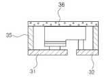
도1을 참조하면, 본 실시 형태에서 제공되는 발광 소자 패키지는, 하면이 외부로 노출된 제1 및 제2 전극(11, 12)과, 상기 제1 전극(11)상에 배치된 발광 소자(13)와, 상기 제1 및 제2 전극(11, 12)의 상면 일부 영역에 배치되되, 상기 발광 소자(13)의 주변을 둘러싸 실장부를 형성하는 반사벽(15) 및, 상기 반사벽(15)에 의하여 지지되며 상기 실장부의 상부를 덮는 형광 필름(16)을 포함하며, 상기 실장부에는 공기가 충진되어 있는 형태로 제공될 수 있다. 이하에서는 본 실시 형태에서 제공되는 발광 소자 패키지를 이루는 각 구성 요소 및 상호간의 결합관계에 대하여 도1을 계속하여 참조하면서 상세히 설명한다.
Referring to FIG. 1, the light emitting device package provided in the present embodiment includes first and
상기 제1 및 제2 전극(11, 12)은 상기 발광 소자(13)와 전기적으로 연결되어 외부로부터 인가되는 전원을 용이하게 공급할 수 있도록 하면이 노출된 구조로 제공될 수 있으며, 바람직하게는, 넓은 판형으로 제공될 수 있고, 더욱 바람직하게는 제1 및 제2 전극(11, 12) 각각이 상부에서 보았을 때 직사각형의 형상을 이루는 형태가 될 수 있다. 또한, 상기 제1 및 제2 전극(11, 12)은 서로 소정 간격을 두고 이격된 형태로 제공되는데, 예를 들어, 제1 및 제2 전극(11, 12) 각각이 상부에서 보았을 때 직사각형 형태를 이루면서, 서로 일 변을 마주하면서 나란히 배치된 형태로 제공될 수 있다. 이와 같이 함으로써, 제1 및 제2 전극(11, 12)은 물리적으로 이격되어 절연될 수 있고, 또한 바람직하게는, 그 사이에 광반사물질이 형성되어 추가적인 기술적 효과를 기대할 수 있는데, 자세한 사항은 후술한다.The first and
또한 이 경우, 상기 제1 및 제2 전극(11, 12)을 이루는 소재로서는, 전기 전도성이 높은 물질, 예를 들어, Cu등을 사용할 수 있으며, 이외에도 투광성을 가지는 물질, 예를 들어 ITO(Indium Tin Oxide)등을 사용할 수 있을 것이다.
In this case, a material having high electrical conductivity, such as Cu, may be used as a material forming the first and
상기 발광 소자(13)는 상기 제1 전극(11) 상에 배치될 수 있다. 본 실시예에서는, 상기 발광 소자(13)와 상기 제1 및 제2 전극(11, 12)의 전기적 연결이 2 개의 도전성 와이어(14)를 통하여 이루어지는 형태로 제공될 수 있다. 그러나, 본 발명은 이에 한정되는 것은 아니며, 실시 형태에 따라 한 개의 도전성 와이어를 형성할 수도 있고, 솔더층을 이용하여 연결되는 형태이거나, 또는 발광 소자 자체가 직접 제1 및 제2 전극(11, 12)와 전기적 연결을 형성하도록 제공될 수도 있을 것이다.
The
상기 반사벽(15)은 상기 제1 및 제2 전극(11, 12)상에 형성되어, 발광 소자 패키지의 측면을 형성하고, 동시에 상기 발광 소자(13)를 둘러싸는 형태로 제공된다. 이 경우, 바람직하게는, 상기 반사벽(15)은 상부에서 보았을때 직사각형 형상을 이루면서 사면을 감싸 일정 공간을 형성하는 벽체의 형상을 갖는다. 이와 같이 함으로써, 복수의 발광 소자(13)를 생산함에 있어 유리한 효과를 얻을 수 있는데, 자세한 사항은 후술한다. 또한, 본 실시예에서는 상기 반사벽(15)이 모든 높이에서 일정한 폭으로 형성되는 것으로 예시되었으나, 본 발명은 반드시 이에 한정되는 것은 아니며, 실시 형태에 따라 다양한 형태의 반사벽 형성이 가능하다.The
또한, 상기 반사벽(15)은, 예를 들어, 실리콘에 분산제를 첨가하여 사출을 통하여 형성할 수 있으며, 그 밖에 공지된 방법을 이용하여 형성할 수 있을 것이다.
In addition, the
상기 형광필름(16)은 상기 반사벽(15)상에 형성되며, 상기 반사벽(15)이 상기 발광 소자(13)를 둘러싸서 형성한 공간 위를 덮으면서 상기 발광 소자(13)가 상부로 방출하는 빛 또는 상기 반사벽(13)에서 반사된 빛이 입사되어, 내부에 분산된 형광체를 통하여 산란될 수 있는 구조로 제공될 수 있다. 즉, 상기 반사벽(15)이 형성한 벽체에 의하여 지지되면서 배치되는 형태로 구성될 수 있다. 이와 같이 상기 형광필름(16)은 반사벽과 접착되는 부분 이외에는 지지되는 부분이 없으므로, 상기 형광필름(16)자체의 강도 및 상기 반사벽(16)으로 둘러싸여 형성되는 공간의 폭을 적절히 형성함으로써 반도체 패키지의 내구성이 충분히 보장될 수 있도록 하는 것이 바람직하다.The
또한 상기 형광필름(16)은 복수의 필름이 다층 적층되어 형성될 수 있으며, 상기 발광 소자에서 방출된 빛에 대하여 파장 변환이 가능하도록 형성될 수 있다.또한, 예를 들어, 봉지재 및 그 내부에 혼합된 형광체를 포함하는 형태로 제공될 수 있다. 이와 같은 형광 필름의 상세한 구성에 대하여는 상기 형광 필름의 제조 방법을 설명하면서 후술하기로 한다.In addition, the
이와 같이 형광필름(16)을 이용한 구성을 채택함으로써, 종래기술에 비하여 색편차를 줄이는 효과를 얻을 수 있다. 즉, 종래의 발광 소자 패키지에서는 발광 소자의 주변 영역을 몰딩 수지로 밀봉함으로써 공정 중 몰딩 수지에 가해지는 열에 따라 형광체의 분산 정도가 달라져 색편차가 발생되는 문제점이 있으나, 몰딩 수지를 사용하지 않는 본 실시예에서는 이와 같은 문제점이 해결된다.
By adopting the configuration using the
또한, 상기 제1 및 제2 전극(11, 12)과, 상기 반사벽(15) 및 상기 형광 필름(16)의 측면은 각각 상기 발광 소자 패키지의 측면을 구성하는데, 본 실시 형태의 경우 상기 세 구성 요소의 측면이 공면(co-plane)을 이루는 형태로 제공될 수 있다. 구체적으로, 상기 제1 및 제2 전극(11, 12)과, 상기 반사벽(15) 및 상기 형광 필름(16)은 순차 적층되며, 상기 세 구성 요소가 중첩되는 영역에서 수직 방향으로 절단된 형태로 제공됨으로써, 상술한 바와 같이 공면을 이루는 형태로 제공될 수 있다. 이와 같이 함으로써 발광 소자 패키지는 균일한 형태의 측면을 형성할 수 있어 대량생산에 유리한 효과를 얻을 수 있고, 광추출효율 면에서도 의도하지 않는 난반사나 굴절등에 대한 영향을 최소화하여 고품질의 발광 소자 패키지의 제작이 가능하다.
In addition, side surfaces of the first and
이하에서는 본 발명에서 제공하는 발광 소자 패키지에 대하여 예시될 수 있는 다양한 실시 형태에 대하여 도면을 참조하여 상세히 설명한다.
Hereinafter, various exemplary embodiments of the light emitting device package provided by the present invention will be described in detail with reference to the accompanying drawings.
도2 내지 도5는 본 발명의 일 실시 형태에 따른 발광 소자 패키지를 개략적으로 나타낸 단면도이다.
2 to 5 are cross-sectional views schematically showing a light emitting device package according to an embodiment of the present invention.
도2를 참조하면, 본 실시 형태에서 제공하는 발광 소자 패키지는, 상기 발광 소자가 길이방향으로 배열되면서 복수개 배치되되, 상기 제1 및 제2 전극을 통하여 서로 전기적으로 직렬 연결되고, 상기 반사벽은 상기 복수개의 발광 소자 각각을 둘러싸는 복수개의 실장부를 형성하는 형태로 제공될 수 있다. 구체적으로, 어느 한 발광 소자와 전기적으로 연결되는 제2 전극은, 그와 이웃한 발광 소자 패키지에서는 제1전극으로서 정의되어 전기적으로 연결되는 형태로 제공될 수 있다. 즉, 상기 제1 및 제2 전극(21, 22)은, 길이방향으로 배열된 발광 소자 패키지간을 직렬로 연결시키는 전류의 통로 역할을 할 수 있다.Referring to FIG. 2, a plurality of light emitting device packages provided in the present embodiment may be disposed while the light emitting devices are arranged in a longitudinal direction, and are electrically connected in series to each other through the first and second electrodes. It may be provided in the form of forming a plurality of mounting portion surrounding each of the plurality of light emitting elements. In detail, the second electrode electrically connected to any one of the light emitting devices may be provided in a form in which the second electrode is defined as the first electrode and electrically connected to the adjacent light emitting device package. That is, the first and
또한, 바람직하게는 상기 제1 및 제2 전극은 행과 열을 이루면서 규칙적으로 배열될 수 있으며, 이와 같이 함으로써 넓은 면적에 행과 열을 이루는 발광 소자 패키지를 동시에 생산하여 생산 효율을 높일 수 있다.In addition, preferably, the first and second electrodes may be regularly arranged in rows and columns. In this way, the production efficiency may be improved by simultaneously producing light emitting device packages having rows and columns in a large area.
또한, 상기 반사벽(25)역시 하나의 발광 소자 패키지(23)와 그와 이웃한 발광 소자 패키지 사이에서 공유될 수 있고, 상기 형광 필름(26)은 발광 소자 패키지 전체를 덮는 단일한 형광 필름(26)의 형태로 제공될 수 있다.
In addition, the
도3을 참조하면, 본 발명의 일 실시 형태에 따른 발광 소자 패키지는, 광 추출 효율의 향상을 위하여 하부 방향으로 두 개의 전극을 가지면서 각 전극이 제1 및 제2 전극(51, 52)에 각각 접속하는 형태로 제공될 수도 있다. 또한, 발광 소자의 일측 및 이와 대향하는 타측에 각각 하나씩의 전극을 구비하는 형태로 실시될 수도 있을 것이다. 이와 같이, 본 발명이 제공하는 발광 소자 패키지는 특정한 형태의 발광 소자에 적용될 수 있도록 한정되는 것이 아니고, 상술한 바와 같이 다양한 형태의 발광 소자에 있어서도, 상기 제1 및 제2 전극(51, 52)이 상기 발광 소자의 전극과 전기적 연결이 이루어질 수 있는 구성이라면 적용될 수 있을 것이다.Referring to FIG. 3, the light emitting device package according to the exemplary embodiment of the present invention has two electrodes in the downward direction for improving light extraction efficiency, and each electrode is provided to the first and
또한, 이와 같은 경우에는 상기 형광필름(16)을 상기 반도체 발광 소자(13)표면에 직접 접착하여 패키지를 견고하게 구성하고 및 고른 광 분포를 실현시키는 구조로 제공될 수도 있을 것이다.
In this case, the
도4를 참조하면, 본 발명의 일 실시 형태에 따른 발광 소자 패키지는, 반사벽(45)을 상기 제1 및 제2 전극(41, 42)에 가까운 영역은 넓은 폭으로 형성하고, 위로 갈수로 작은 폭으로 형성하여 상기 발광 소자(43)로부터 방출되는 빛이 용이하게 반사되어 발광 소자 패키지 상부로 방출될 수 있도록 하는 형태로 제공될 수 있다. 그러나, 상기 발광 소자(43)에서 방출되는 측면광을 반사시키기 용이한 형태라면, 반드시 본 실시 형태에서와 같이 단면이 사다리꼴 형상을 갖는 형태로 제공될 필요는 없으며, 예를 들어, 완만한 곡선을 이루면서 상기 발광 소자가 형성된 영역을 초점으로 갖는 반포물선 형태의 측면을 구비하도록 제공될 수도 있을 것이다.
Referring to FIG. 4, in the light emitting device package according to the exemplary embodiment of the present invention, the
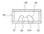
도5를 참조하면, 본 발명의 일 실시 형태에 따른 발광 소자 패키지는, 상기 제1 및 제2 전극(51, 52)이 서로 소정 간격을 두고 이격된 형태로 제공되는데, 이와 같이 이격되어 형성된 공간에 광반사물질(55A)이 형성된 형태로 제공될 수 있다. 이와 같이 함으로써, 상기 광반사물질(55A)에 입사되는 빛을 반사하여 상기 광반사물질(55A)이 형성되지 않은 경우에 비하여 광추출효율을 향상시킬 수 있다.Referring to FIG. 5, in the light emitting device package according to the exemplary embodiment of the present invention, the first and
또한 바람직하게는, 상기 광반사물질(55A)은 상기 반사벽(55)와 동일한 물질로 이루어질 수 있어, 별도의 공정을 마련하지 않고도 상기 반사벽(55)의 형성과 동시에 상기 광반사물질(55A)을 형성하여 공정을 단순화할 수 있다.
Also, preferably, the
도6은, 본 발명의 일 실시 형태에 따른 발광 소자 패키지 제조 방법을 단계별로 나타낸 단면도이다. 이 경우, 도6a는 제1 및 제2 전극을 형성하는 과정을, 도6b는 상기 제1 및 제2 전극 상에 반사벽을 형성하는 단계를, 도6c는 상기 제1 및 제2 전극 상에 발광 소자를 실장하는 단계를, 도6d는 상기 반사벽 상에 형광 필름을 부착하는 단계를, 도6e는 상기 반사벽을 두께방향으로 절단하여 적어도 하나 이상의 발광 소자 패키지를 획득하는 단계를 각각 나타낸다.
6 is a cross-sectional view showing step by step a method of manufacturing a light emitting device package according to an embodiment of the present invention. In this case, FIG. 6A illustrates a process of forming first and second electrodes, FIG. 6B illustrates a process of forming reflective walls on the first and second electrodes, and FIG. 6C illustrates the first and second electrodes. 6D illustrates attaching a fluorescent film on the reflective wall, and FIG. 6E illustrates cutting the reflective wall in a thickness direction to obtain at least one light emitting device package.
우선 도6a를 참조하면, 본 발명의 일 실시 형태에 따른 발광 소자 패키지 제조 방법은, 제1 및 제2 전극(61, 62)을 평면상에 형성하는 단계로 제공될 수 있다. 이 경우, 상기 '제1 및 제2'의 표현은 이해를 돕기 위하여 도면상에서 가장 우측에 위치한 한 쌍의 전극을 기준으로 한 것이며, 발광 소자 패키지 각각에서 정의되는 모든 제1 및 제2 전극을 대표하는 개념임에 유의하여야 한다.First, referring to FIG. 6A, a method of manufacturing a light emitting device package according to an exemplary embodiment of the present disclosure may be provided by forming first and
또한, 상기 제1 및 제2 전극(61, 62)은, 상면에서 보았을 때 직사각형을 이루는 복수의 도금판을 사이에 일정 거리를 이격하여 공간을 갖는 형태로 형성하여 반복되는 구성을 갖도록 할 수 있는데, 각각은 동일한 형상을 가지면서 일정 패턴을 이루면서 길이방향으로 배열될 수 있고, 바람직하게는 행과 열을 이루면서 배치되어 형성되는 것이 바람직하다.In addition, the first and
또한, 상기 제1 및 제2 전극(61, 62)의 형성을 위해, 기판을 형성하고 상기 기판 상에 제1 및 제2 전극(61, 62)을 형성시키도록 제공될 수 있다.
In addition, to form the first and
다음으로, 도6b를 참조하면, 상기 제1 및 제2 전극(61, 62) 상에 반사벽(65)을 형성할 수 있고, 상기 반사벽(65)은 일정한 공간이 형성되도록 둘러싸는 벽면의 형상을 갖도록 할 수 있으며, 바람직하게는 상부에서 보았을 때 직사각형 형상을 갖도록 제공될 수 있다. 또한 상기 반사벽(65)은, 상기 제1 전극 및 제2 전극(61, 62)에 대응하여 동일한 패턴으로 형성되는 것이 바람직하며, 도시되지는 않았으나, 상기 제1 및 제2 전극(61, 62) 사이의 공간에 상기 반사벽(65)과 동일한 구성성분을 갖는 광반사물질을 추가로 형성하는 단계를 포함할 수 있다.
Next, referring to FIG. 6B, a
다음으로, 도6c를 참조하면, 상기 제1 및 제2 전극(61, 62) 상에 발광 소자(63)를 실장하는 단계로 제공될 수 있다. 이 경우, 상기 발광 소자(63)는, 상기 반사벽(65)으로 둘러싸여 이루어진 하나의 공간에 하나의 발광 소자(63)가 실장되도록 하는 것이 바람직하다. 이와 같이 구성함으로써, 상기 제1 및 제2 전극(61, 62), 상기 반사벽(65) 및 상기 반사벽(65)으로 둘러싸여 형성되는 공간에 실장되는 발광 소자(63)가 각각 대응되어 독자적인 발광 소자 패키지를 구성할 수 있다.Next, referring to FIG. 6C, the
또한 본 실시예에서는 일측 면에 두 개의 전극이 형성된 발광 소자와 상기 발광 소자의 전극 및 제1 및 제2 전극과 전기적으로 연결되는 도전성 와이어로 이루어진 구성을 예시하였으나, 본 발명은 이에 한정하지 아니하고 다양한 형태의 발광 소자 및 전기적 연결 수단을 포함하여 실시될 수 있다.
In addition, in the present exemplary embodiment, a light emitting device having two electrodes formed on one side thereof and a conductive wire electrically connected to the electrodes of the light emitting device and the first and second electrodes are illustrated, but the present invention is not limited thereto. It can be implemented including a light emitting device of the form and electrical connection means.
다음으로, 도6d를 참조하면, 상기 반사벽(65) 상에 실장부의 상부를 덮도록 상기 형광 필름(66)을 접착하는 단계가 제공될 수 있다. 여기서 상기 형광 필름(66)은 일체로 형성된 단일의 형광 필름(66)인 것이 바람직하며, 이와 같이 함으로써 단일한 공정으로 상기 형광 필름(66)의 부착을 완료할 수 있고, 나아가 상기 반사벽(65) 상에 견고하게 부착되는 효과를 기대할 수 있다.
Next, referring to FIG. 6D, the step of adhering the
다음으로, 도6e를 참조하면, 상기 반사벽(65)이 형성된 영역을 두께방향으로 절단하여 적어도 하나 이상의 발광 소자 패키지를 획득하는 단계가 제공될 수 있다. 이 경우, 바람직하게는 상기 절단면은 상기 제1 및 제2 전극(61, 62)과 수직 방향의 직선형태로서, 상기 제1 및 제2 전극(61, 62)과, 상기 반사벽(65)과, 상기 형광 필름(66)이 모두 공면(co-plane)을 이루면서 발광 소자 패키지의 측면을 형성하도록 절단하는 것이 바람직하다. 이와 같이 함으로써, 본 공정을 통하여 획득되는 각 발광 소자 패키지는 그 외부 형태가 모두 균일하도록 규격화된 형태로 얻어질 수 있다.
Next, referring to FIG. 6E, a step of obtaining at least one light emitting device package by cutting the region in which the
상기와 같은 과정을 통하여 얻어지는 발광 소자 패키지는, 내부에 몰딩 수지를 충진하지 아니하고 형광 필름(66)을 사용하여 공정 과정에서 발생할 수 있는 열에 의한 색편차 문제를 해결할 수 있으며, 상기 제1 및 제2 전극(61, 62), 상기 반사벽(65) 및 상기 형광 필름(66) 각각을 한꺼번에 복수개 패턴을 이루도록 제작한 후, 일정 간격으로 절단함으로써 개별적으로 패키지를 생산하는 경우에 비하여 생산 효율을 증대할 수 있다.
The light emitting device package obtained through the above process may solve the color deviation problem due to heat that may occur in the process process by using the
도7a 내지 도7c는, 본 발명의 일 실시 형태에 따른 발광 소자 패키지에서 형광필름의 제조방법을 나타낸 공정 단면도이다.
7A to 7C are cross-sectional views illustrating a method of manufacturing a fluorescent film in a light emitting device package according to an embodiment of the present invention.
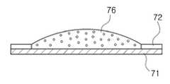
우선, 도 7a에 도시된 바와 같이, 형광필름을 형성할 필름(71)을 준비한 후, 상기 필름(71) 상에 형광필름을 형성하고자 하는 영역이 오픈된 마스크(72)를 준비한다. 그리고, 상기 마스크(72)에 의해 노출된 상기 필름(71) 상에 디스펜싱 등의 방법을 통해 형광체를 포함하는 혼합 봉지재(76)를 도포한다.First, as shown in FIG. 7A, after preparing a
본 실시 형태에서는, 상기 혼합 봉지재(76)는 제2 액상 봉지재에 형광체가 혼합된 것으로 제공될 수 있다. 여기서, 제2 액상 봉지재란, 열경화성 수지를 포함하고 있는 봉지재를 의미하며, 에폭시, 실리콘, 변형 실리콘, 우레탄수지, 옥세탄수지, 아크릴, 폴리카보네이트, 및 폴리이미드 중 어느 하나를 포함할 수 있다.
In the present embodiment, the
다음으로, 도7b에 도시된 바와 같이, 닥터 블레이드(74)를 사용하며, 상기 필름(71) 상에 도포된 혼합 봉지재(76)의 표면을 평평하게 밀어줌으로써, 상기 필름(71) 상에 도포된 혼합 봉지재(76)의 두께를 균일하게 해준다.
Next, as shown in FIG. 7B, the
다음으로, 도7c를 참조하면, 상기 필름(71)에 균일한 두께로 도포된 혼합 봉지재(76)를 경화시킨 후, 상기 마스크(72)를 제거함으로써, 형광체가 균일하게 분산된 형광필름을 제작한다.
Next, referring to FIG. 7C, after curing the
상기한 바와 같이 제작된 형광필름은 상술한 바와 같이, 반사벽 혹은 발광 소자 상에 부착되는데, 이때, 상기 형광필름은 접착제 등을 사용하여 부착할 수 있다.The fluorescent film produced as described above is attached to the reflective wall or the light emitting device, as described above, wherein the fluorescent film may be attached using an adhesive or the like.
한편, 형광필름을 제작하기 위해 사용되는 혼합 봉지재(76)는 제2 액상 봉지재 이외에도, 경화제를 포함하지 않는 제1 액상 봉지재 또는, UV 경화제를 포함하는 UV 봉지재를 사용할 수도 있다.On the other hand, the
이와 같이 제1 액상 봉지재 또는 혼합 봉지재를 사용하는 경우, 필름 상에 도포된 혼합 봉지재를 바로 경화하지 않고, 그 표면에 또 다른 필름을 입힌 후, 이를 냉장 혹은 냉동 보관하게 되며, 추후에 필름을 제거하고, 반사벽 혹은 발광 소자 상에 부착시킨 후, 열경화 공정을 통해, 상기 봉지재와 접착된다.When using the first liquid encapsulant or mixed encapsulant as described above, the mixed encapsulant applied on the film is not immediately cured, and another film is coated on the surface thereof, and then it is refrigerated or frozen and then stored. The film is removed, adhered onto the reflective wall or the light emitting element, and then adhered to the encapsulant through a thermosetting process.
또한, UV 봉지재를 포함하는 혼합 봉지재의 경우에도, UV 경화를 통해 반사벽 혹은 발광 소자 상에 부착될 수 있다.In addition, even in the case of a mixed encapsulant including the UV encapsulant, it may be attached onto the reflective wall or the light emitting device through UV curing.
또한, 본 실시예에서는 마스크를 이용하여 형광 필름을 형성하는 것으로 예시되었으나, 실시 형태에 따라, 마스크를 사용하지 않고, 대형의 형광필름을 제작한 후, 이를 필요한 크기로 잘라서 사용하는 것도 가능하다는 점은 해당 기술분야에서 통상의 지식을 가진 자에게는 용이하게 이해될 수 있을 것이다.In addition, in the present embodiment, it was illustrated that a fluorescent film is formed using a mask, but according to the embodiment, it is also possible to cut and use a fluorescent film of a large size without using a mask, and then cut it to a required size. Will be readily understood by those of ordinary skill in the art.
상기한 바와 같이, 본 발명은, 형광체를 필름형태로 제작한 후, 이를 반사벽 혹은 발광 소자 상에 부착함으로써, 형광체의 균일한 분산을 가능하도록 하여 색 균일도를 향상시킨다. 즉, 종래에는, 디스펜싱 방식을 통해 봉지재를 형성하기 때문에, 투명수지에 혼합되어 있는 형광체의 침전으로 인해 봉지재 내부의 형광체의 농도가 불균일하게 분포되어 색균일도가 떨어지는 문제가 있었으나, 본 발명에서는 얇은 시트 형태의 형광필름을 제작함으로써, 형광필름 내의 형광체의 침전을 원천적으로 차단하고, 필름 내의균일한 형광체의 분포를 통해, 색의 균일도를 향상시키고, 색 재현성을 높일 수 있는 효과를 달성할 수 있다.
As described above, according to the present invention, the fluorescent substance is produced in the form of a film, and then attached to the reflective wall or the light emitting device to enable uniform dispersion of the fluorescent substance, thereby improving color uniformity. That is, in the related art, since the encapsulant is formed through the dispensing method, the concentration of the phosphor in the encapsulant is unevenly distributed due to the precipitation of the phosphor mixed in the transparent resin, thereby decreasing the color uniformity. In the present invention, a thin sheet-shaped fluorescent film is produced, thereby preventing the precipitation of the phosphor in the fluorescent film at the source and improving the uniformity of the color and improving the color reproducibility through the uniform distribution of the phosphor in the film. Can be.
본 발명의 기본 개념은 발광 소자 패키지를 제작함에 있어서, 몰딩 수지를 사용하지 않고, 균일한 두께의 형광필름을 별도로 제작한 후, 이를 발광 소자 칩의 반사벽 상에 부착하여 사용하는 것으로, 발광 소자의 실장방식 및 이의 패키지 구조에 상관없이 형광필름을 별도 제작하고 몰딩 수지를 사용하지 않는 것이라면, 본 발명에 모두 포함될 것이다.The basic concept of the present invention is to manufacture a light emitting device package, and to manufacture a fluorescent film having a uniform thickness without using a molding resin, and then attach it to a reflective wall of a light emitting device chip to use the light emitting device. Irrespective of the mounting method and its package structure, if the fluorescent film is manufactured separately and does not use a molding resin, all will be included in the present invention.
또한, 본 발명은 상술한 실시형태 및 첨부된 도면에 의해 한정되는 것이 아니며, 첨부된 청구범위에 의해 한정된다. 따라서, 청구범위에 기재된 본 발명의 기술적 사상을 벗어나지 않는 범위 내에서 다양한 형태의 치환, 변형 및 변경이 가능하다는 것은 당 기술분야의 통상의 지식을 가진 자에게는 자명할 것이며, 이 또한 첨부된 청구범위에 기재된 기술적 사상에 속한다 할 것이다.In addition, the present invention is not limited by the above-described embodiment and the accompanying drawings, but by the appended claims. Therefore, it will be apparent to those skilled in the art that various forms of substitution, modification, and alteration are possible without departing from the technical spirit of the present invention described in the claims, and the appended claims. Will belong to the technical spirit described in.
11, 21, 31, 41, 51, 61: 제1 전극12, 22, 32, 42, 52, 62: 제2 전극
13, 23, 33, 43, 53, 63: 발광 소자14, 24, 44, 54, 64: 도전성 와이어
15, 25, 35, 45, 55, 65: 반사벽16, 26, 36, 46, 56, 66: 형광 필름
71: 필름72: 마스크
76: 혼합 봉지재11, 21, 31, 41, 51, 61:
13, 23, 33, 43, 53, 63:
15, 25, 35, 45, 55, 65:
71: film 72: mask
76: mixed encapsulant
Claims (27)
Translated fromKorean상기 제1 및 제2 전극 중 적어도 하나의 상면에 배치되는 발광 소자;
상기 제1 및 제2 전극의 상면에 배치되되 상기 발광 소자의 주변을 둘러싸 실장부를 형성하는 반사벽; 및
상기 반사벽 상에 배치되어 상기 실장부의 상부를 덮는 형광 필름;
을 포함하는 발광 소자 패키지.First and second electrodes having at least a portion of a lower surface exposed to the outside;
A light emitting device disposed on an upper surface of at least one of the first and second electrodes;
A reflection wall disposed on upper surfaces of the first and second electrodes and surrounding the periphery of the light emitting device to form a mounting portion; And
A fluorescent film disposed on the reflective wall to cover an upper portion of the mounting part;
Light emitting device package comprising a.
상기 제1 및 제2 전극, 상기 반사벽 및 상기 형광 필름이 적어도 일부 영역에서 서로 공면(co-plane)을 이루어 형성되는 측면을 갖는 것을 특징으로 하는 발광 소자 패키지.The method of claim 1,
The light emitting device package of claim 1, wherein the first and second electrodes, the reflective wall, and the fluorescent film have co-planes formed in at least some regions.
상기 발광 소자는 도전성 와이어를 통하여 상기 제1 및 제2 전극과 전기적으로 연결된 것을 특징으로 하는 발광 소자 패키지.The method of claim 1,
The light emitting device package of claim 1, wherein the light emitting device is electrically connected to the first and second electrodes through a conductive wire.
상기 발광 소자는 솔더층을 통하여 상기 제1 및 제2 전극과 전기적으로 연결된 것을 특징으로 하는 발광 소자 패키지.The method of claim 1,
The light emitting device package of claim 1, wherein the light emitting device is electrically connected to the first and second electrodes through a solder layer.
상기 발광 소자는 복수개 배치되되, 상기 제1 및 제2 전극을 통하여 서로 전기적으로 연결되고, 상기 반사벽은 상기 복수개의 발광 소자 각각을 둘러싸는 복수개의 실장부를 형성하는 것을 특징으로 하는 발광 소자 패키지.The method according to claim 1,
A plurality of light emitting devices are disposed, the light emitting device package, characterized in that the first and second electrodes are electrically connected to each other, the reflective wall forms a plurality of mounting portion surrounding each of the plurality of light emitting devices.
상기 제1 및 제2 전극은 서로 거리를 두고 이격되어 사이에 공간을 형성하며 상기 공간에는 광반사물질이 형성되는 것을 특징으로 하는 발광 소자 패키지.The method of claim 1,
The first and second electrodes are spaced apart from each other to form a space therebetween, the light emitting device package, characterized in that the light reflecting material is formed in the space.
상기 광반사물질은 상기 반사벽과 동일한 소재로 이루어진 것을 특징으로 하는 발광 소자 패키지.The method of claim 5,
The light reflecting material is a light emitting device package, characterized in that made of the same material as the reflective wall.
상기 형광 필름은 복수의 필름이 다층 적층되어 이루어지는 것을 특징으로 하는 발광 소자 패키지.The method of claim 1,
The fluorescent film is a light emitting device package, characterized in that a plurality of films are laminated in a stack.
상기 형광 필름은 상기 발광 소자에서 방출된 빛을 황색, 적색 및 녹색 중 적어도 하나로 파장을 변환시키는 것을 특징으로 하는 발광 소자 패키지.The method of claim 1,
The fluorescent film is a light emitting device package, characterized in that for converting the wavelength of the light emitted from the light emitting device to at least one of yellow, red and green.
상기 형광 필름은 봉지재 및 그 내부에 혼합된 형광체를 포함하여 이루어지는 것을 특징으로 하는 발광 소자 패키지.The method of claim 1,
The fluorescent film comprises an encapsulant and a phosphor mixed therein.
상기 반사벽은 상기 발광 소자 주변을 사각형으로 둘러싸는 것을 특징으로 하는 발광 소자 패키지.The method of claim 1,
The reflective wall is a light emitting device package, characterized in that surrounding the light emitting device around the rectangle.
상기 제1 및 제2 전극은 투광성을 갖는 물질로 이루어진 것을 특징으로 하는 발광 소자 패키지.The method of claim 1,
The first and second electrodes are light-emitting device package, characterized in that made of a light transmitting material.
상기 반사벽은 실리콘에 분산제가 첨가된 것을 특징으로 하는 발광 소자 패키지.The method of claim 1,
The reflective wall is a light emitting device package, characterized in that the dispersant is added to the silicon.
상기 실장부에는 공기가 충진된 것을 특징으로 하는 발광 소자 패키지.The method of claim 1,
Light emitting device package, characterized in that the mounting portion is filled with air.
상기 형광 필름의 적어도 일부는 상기 발광 소자에 접착되는 것을 특징으로 하는 발광 소자 패키지.The method of claim 1,
At least a portion of the fluorescent film is a light emitting device package, characterized in that adhered to the light emitting device.
제1 및 제2 전극을 형성하는 단계;
상기 제1 및 제2 전극 상면의 적어도 일부 영역에 반사벽을 형성하여 상기 반사벽으로 둘러싸이며 상부가 외부로 연결된 실장부를 형성하는 단계;
상기 실장부 내부에 발광 소자를 배치하는 단계;
상기 반사벽 상에 실장부의 상부를 덮도록 상기 형광 필름을 접착하는 단계;
를 포함하는 발광 소자 패키지 제조 방법.Preparing a fluorescent film in which phosphors are dispersed;
Forming first and second electrodes;
Forming a mounting wall on at least some regions of the upper surfaces of the first and second electrodes to form a mounting portion surrounded by the reflective wall and connected to an outside thereof;
Disposing a light emitting device in the mounting unit;
Bonding the fluorescent film to cover an upper portion of a mounting part on the reflective wall;
Light emitting device package manufacturing method comprising a.
상기 형광필름을 준비하는 단계는,
제1 및 제2 필름을 준비하는 단계;
제1 액상 봉지재와 형광체를 혼합하여 혼합 봉지재를 준비하는 단계;
상기 혼합 봉지재를 상기 제1 필름 상에 균일한 두께로 형성하는 단계;
상기 제1 필름 상에 형성된 상기 혼합 봉지재 표면에 상기 제2 필름을 부착하는 단계; 및
상기 제1 및 제2필름이 부착된 상기 혼합 봉지재를 냉장 또는 냉동 보관하는 단계;
를 포함하는 발광 소자 패키지 제조 방법.The method of claim 16,
Preparing the fluorescent film,
Preparing first and second films;
Preparing a mixed encapsulant by mixing the first liquid encapsulant and the phosphor;
Forming the mixed encapsulant to a uniform thickness on the first film;
Attaching the second film to the surface of the mixed encapsulant formed on the first film; And
Refrigerating or freezing the mixed encapsulant having the first and second films attached thereto;
Light emitting device package manufacturing method comprising a.
상기 반사벽 상에 상기 형광 필름을 접착하는 단계는,
상기 제1 또는 제2필름을 제거하는 단계;
상기 혼합 봉지재를 상기 반사벽 상에 부착시키는 단계; 및
상기 혼합 봉지재를 경화시켜, 상기 반사벽 상에 접착시키는 단계;
를 포함하는 발광 소자 패키지 제조 방법.The method of claim 17,
Bonding the fluorescent film on the reflective wall,
Removing the first or second film;
Attaching the mixed encapsulant onto the reflective wall; And
Curing the mixed encapsulant and attaching the mixed encapsulant to the reflective wall;
Light emitting device package manufacturing method comprising a.
상기 형광필름을 준비하는 단계는,
필름을 준비하는 단계;
제2 액상 봉지재와 형광체를 혼합하여 혼합 봉지재를 준비하는 단계;
상기 혼합 봉지재를 상기 필름 상에 균일한 두께로 형성하는 단계; 및
상기 혼합 봉지재를 경화시키는 단계;
를 포함하는 발광 소자 패키지 제조 방법.The method of claim 16,
Preparing the fluorescent film,
Preparing a film;
Preparing a mixed encapsulant by mixing the second liquid encapsulant and the phosphor;
Forming the mixed encapsulant to a uniform thickness on the film; And
Curing the mixed encapsulant;
Light emitting device package manufacturing method comprising a.
상기 반사벽 상에 상기 형광 필름을 접착하는 단계는,
접착제를 통해 상기 경화된 혼합 봉지재를 상기 반사벽 상에 접착시키는 것을 특징으로 하는 발광 소자 패키지 제조 방법.20. The method of claim 19,
Bonding the fluorescent film on the reflective wall,
And bonding the cured mixed encapsulant onto the reflective wall through an adhesive.
상기 형광필름을 준비하는 단계는,
제1 및 제2 필름을 준비하는 단계;
UV 경화제를 포함하는 봉지재와 형광체를 혼합하여 혼합 봉지재를 준비하는 단계;
상기 혼합 봉지재를 상기 제1필름 상에 균일한 두께로 형성하는 단계;
상기 제1필름 상에 형성된 상기 혼합 봉지재 표면에 상기 제2필름을 부착하는 단계; 및
상기 제1 및 제2필름이 부착된 상기 혼합 봉지재를 냉장 또는 냉동 보관하는 단계;
를 포함하는 발광 소자 패키지 제조 방법.The method of claim 16,
Preparing the fluorescent film,
Preparing first and second films;
Preparing a mixed encapsulant by mixing an encapsulant including a UV curing agent and a phosphor;
Forming the mixed encapsulant to a uniform thickness on the first film;
Attaching the second film to a surface of the mixed encapsulant formed on the first film; And
Refrigerating or freezing the mixed encapsulant having the first and second films attached thereto;
Light emitting device package manufacturing method comprising a.
상기 반사벽 상에 형광필름을 접착시키는 단계는,
상기 제1 또는 제2필름을 제거하는 단계;
상기 혼합 봉지재를 상기 반사벽 상에 부착시키는 단계; 및
상기 혼합 봉지재를 UV 경화를 통해, 상기 반사벽 상에 접착시키는 단계;
를 포함하는 발광 소자 패키지 제조 방법.The method of claim 21,
Bonding the fluorescent film on the reflective wall,
Removing the first or second film;
Attaching the mixed encapsulant onto the reflective wall; And
Adhering the mixed encapsulant onto the reflective wall through UV curing;
Light emitting device package manufacturing method comprising a.
상기 제1 및 제2 전극과, 상기 반사벽 및 상기 형광 필름이 적어도 일부 영역에서 서로 공면(co-plane)을 이루도록 중첩된 영역을 두께방향으로 절단하여, 적어도 하나 이상의 발광 소자 패키지를 획득하는 단계를 더 포함하는 것을 특징으로 하는 발광 소자 패키지 제조 방법.The method of claim 16,
Obtaining at least one light emitting device package by cutting the overlapped regions in a thickness direction such that the first and second electrodes, the reflective wall, and the fluorescent film are co-plane with each other in at least some regions Light emitting device package manufacturing method comprising a further.
상기 획득된 발광 소자 패키지는, 상기 발광 소자가 복수개 배치되어 상기 제1 및 제2 전극을 통하여 서로 전기적으로 연결되고, 상기 반사벽이 상기 복수개의 발광 소자 각각을 둘러싸서 형성하는 복수개의 실장부가 포함되도록 절단하는 것을 특징으로 하는 발광 소자 패키지 제조 방법.The method of claim 23, wherein
The obtained light emitting device package includes a plurality of mounting parts in which a plurality of light emitting devices are disposed and electrically connected to each other through the first and second electrodes, and the reflective wall surrounds each of the plurality of light emitting devices. Method for producing a light emitting device package, characterized in that the cutting to.
상기 실장부를 형성하는 단계는, 상기 반사벽이 상기 발광 소자 주변을 사각형으로 둘러싸도록 형성하는 것을 특징으로 하는 발광 소자 패키지 제조 방법.The method of claim 16,
The forming of the mounting part may include forming the reflective wall so as to surround the light emitting device in a rectangular shape.
상기 발광 소자는, 청색, 적색, 녹색 및 UV 파장을 발생시키는 발광 소자 중 적어도 하나 이상을 포함하는 하는 것을 특징으로 하는 발광 소자 패키지 제조 방법.The method of claim 16,
The light emitting device is a light emitting device package manufacturing method characterized in that it comprises at least one or more of the light emitting device for generating blue, red, green and UV wavelengths.
상기 형광체는, 황색, 적색 및 녹색 중 적어도 하나로 파장을 변환시키는 형광체로 이루어진 것을 특징으로 하는 발광 소자 패키지 제조 방법.The method of claim 16,
The phosphor is made of a phosphor for converting the wavelength to at least one of yellow, red and green light emitting device package manufacturing method.
Priority Applications (5)
| Application Number | Priority Date | Filing Date | Title |
|---|---|---|---|
| KR1020100111706AKR20120050282A (en) | 2010-11-10 | 2010-11-10 | Light emitting device package and method of manufacturing the same |
| US13/290,639US8890188B2 (en) | 2010-11-10 | 2011-11-07 | Light emitting device surrounded by reflection wall and covered with fluorescent film |
| EP11188523.2AEP2453488B1 (en) | 2010-11-10 | 2011-11-10 | Light emitting device package and method of manufacturing the same |
| CN201110372560.6ACN102468417B (en) | 2010-11-10 | 2011-11-10 | Light emitting device package and method of manufacturing the same |
| US14/543,785US9142737B2 (en) | 2010-11-10 | 2014-11-17 | Light emitting device surrounded by reflection wall and covered with fluorescent film |
Applications Claiming Priority (1)
| Application Number | Priority Date | Filing Date | Title |
|---|---|---|---|
| KR1020100111706AKR20120050282A (en) | 2010-11-10 | 2010-11-10 | Light emitting device package and method of manufacturing the same |
Publications (1)
| Publication Number | Publication Date |
|---|---|
| KR20120050282Atrue KR20120050282A (en) | 2012-05-18 |
Family
ID=45094439
Family Applications (1)
| Application Number | Title | Priority Date | Filing Date |
|---|---|---|---|
| KR1020100111706ACeasedKR20120050282A (en) | 2010-11-10 | 2010-11-10 | Light emitting device package and method of manufacturing the same |
Country Status (4)
| Country | Link |
|---|---|
| US (2) | US8890188B2 (en) |
| EP (1) | EP2453488B1 (en) |
| KR (1) | KR20120050282A (en) |
| CN (1) | CN102468417B (en) |
Cited By (2)
| Publication number | Priority date | Publication date | Assignee | Title |
|---|---|---|---|---|
| WO2014182104A1 (en)* | 2013-05-09 | 2014-11-13 | 서울반도체 주식회사 | Light source module and backlight unit having same |
| WO2017116136A1 (en)* | 2015-12-31 | 2017-07-06 | 서울반도체주식회사 | Display device |
Families Citing this family (15)
| Publication number | Priority date | Publication date | Assignee | Title |
|---|---|---|---|---|
| TWI528596B (en)* | 2012-03-16 | 2016-04-01 | 鴻海精密工業股份有限公司 | Light-emitting diode package structure and manufacturing method thereof |
| CN102931180A (en)* | 2012-11-19 | 2013-02-13 | 上舜照明(中国)有限公司 | LED light source and manufacturing method thereof |
| CN103022323A (en)* | 2012-12-10 | 2013-04-03 | 中国海洋大学 | Preparation and application for white light light emitting diode (LED) fluorescent powder prefabricated components |
| DE102012113003A1 (en)* | 2012-12-21 | 2014-04-03 | Osram Opto Semiconductors Gmbh | Method for producing an optoelectronic semiconductor component and optoelectronic semiconductor component |
| KR102075993B1 (en)* | 2013-12-23 | 2020-02-11 | 삼성전자주식회사 | Method of Fabricating White LED Devices |
| US9997676B2 (en) | 2014-05-14 | 2018-06-12 | Genesis Photonics Inc. | Light emitting device and manufacturing method thereof |
| US10439111B2 (en) | 2014-05-14 | 2019-10-08 | Genesis Photonics Inc. | Light emitting device and manufacturing method thereof |
| TWI557952B (en) | 2014-06-12 | 2016-11-11 | 新世紀光電股份有限公司 | Light-emitting element |
| JP2016181689A (en) | 2015-03-18 | 2016-10-13 | 新世紀光電股▲ふん▼有限公司Genesis Photonics Inc. | Light emitting diode structure and method for manufacturing the same |
| TWI657597B (en) | 2015-03-18 | 2019-04-21 | 新世紀光電股份有限公司 | Edge lighting light emitting diode structure and method of manufacturing the same |
| CN106407881B (en)* | 2015-07-29 | 2020-07-31 | 财团法人工业技术研究院 | Biometric identification device and method and wearable carrier |
| US10679081B2 (en)* | 2015-07-29 | 2020-06-09 | Industrial Technology Research Institute | Biometric device and wearable carrier |
| CN106549092A (en) | 2015-09-18 | 2017-03-29 | 新世纪光电股份有限公司 | Light emitting device and method for manufacturing the same |
| CN107968142A (en) | 2016-10-19 | 2018-04-27 | 新世纪光电股份有限公司 | Light-emitting device and its manufacture method |
| CN109994458B (en) | 2017-11-05 | 2022-07-01 | 新世纪光电股份有限公司 | light-emitting device |
Family Cites Families (48)
| Publication number | Priority date | Publication date | Assignee | Title |
|---|---|---|---|---|
| KR100537349B1 (en) | 1996-06-26 | 2006-02-28 | 오스람 게젤샤프트 미트 베쉬랭크터 하프퉁 | Light-emitting semiconductor component with luminescence conversion element |
| DE19638667C2 (en) | 1996-09-20 | 2001-05-17 | Osram Opto Semiconductors Gmbh | Mixed-color light-emitting semiconductor component with luminescence conversion element |
| CN1143394C (en) | 1996-08-27 | 2004-03-24 | 精工爱普生株式会社 | Peeling method, thin film device transfer method and thin film device |
| USRE38466E1 (en) | 1996-11-12 | 2004-03-16 | Seiko Epson Corporation | Manufacturing method of active matrix substrate, active matrix substrate and liquid crystal display device |
| JP3378465B2 (en) | 1997-05-16 | 2003-02-17 | 株式会社東芝 | Light emitting device |
| US7208725B2 (en) | 1998-11-25 | 2007-04-24 | Rohm And Haas Electronic Materials Llc | Optoelectronic component with encapsulant |
| HK1041367A1 (en) | 2000-02-09 | 2002-07-05 | Nippon Leiz Corporation | Light source |
| JP3906654B2 (en) | 2000-07-18 | 2007-04-18 | ソニー株式会社 | Semiconductor light emitting device and semiconductor light emitting device |
| US6747406B1 (en) | 2000-08-07 | 2004-06-08 | General Electric Company | LED cross-linkable phospor coating |
| MY145695A (en)* | 2001-01-24 | 2012-03-30 | Nichia Corp | Light emitting diode, optical semiconductor device, epoxy resin composition suited for optical semiconductor device, and method for manufacturing the same |
| US6737681B2 (en)* | 2001-08-22 | 2004-05-18 | Nichia Corporation | Light emitting device with fluorescent member excited by semiconductor light emitting element |
| US6818465B2 (en) | 2001-08-22 | 2004-11-16 | Sony Corporation | Nitride semiconductor element and production method for nitride semiconductor element |
| JP2003218034A (en) | 2002-01-17 | 2003-07-31 | Sony Corp | Selective growth method, semiconductor light emitting device and method of manufacturing the same |
| JP3815335B2 (en) | 2002-01-18 | 2006-08-30 | ソニー株式会社 | Semiconductor light emitting device and manufacturing method thereof |
| KR100499129B1 (en) | 2002-09-02 | 2005-07-04 | 삼성전기주식회사 | Light emitting laser diode and fabricatin method thereof |
| US7002182B2 (en) | 2002-09-06 | 2006-02-21 | Sony Corporation | Semiconductor light emitting device integral type semiconductor light emitting unit image display unit and illuminating unit |
| KR20050113200A (en) | 2003-02-26 | 2005-12-01 | 크리, 인코포레이티드 | Composite white light source and method for fabricating |
| CN100511732C (en) | 2003-06-18 | 2009-07-08 | 丰田合成株式会社 | Light emitting device |
| US7029935B2 (en) | 2003-09-09 | 2006-04-18 | Cree, Inc. | Transmissive optical elements including transparent plastic shell having a phosphor dispersed therein, and methods of fabricating same |
| KR100714639B1 (en) | 2003-10-21 | 2007-05-07 | 삼성전기주식회사 | Light emitting element |
| KR100506740B1 (en) | 2003-12-23 | 2005-08-08 | 삼성전기주식회사 | Nitride semiconductor light emitting device and method of manufacturing the same |
| US7239080B2 (en) | 2004-03-11 | 2007-07-03 | Avago Technologies Ecbu Ip (Singapore) Pte. Ltd | LED display with overlay |
| DE102005046420B4 (en)* | 2004-10-04 | 2019-07-11 | Stanley Electric Co. Ltd. | A method of manufacturing a semiconductor light-emitting device |
| KR100664985B1 (en) | 2004-10-26 | 2007-01-09 | 삼성전기주식회사 | Nitride-based semiconductor device |
| WO2006087660A1 (en) | 2005-02-17 | 2006-08-24 | Philips Intellectual Property & Standards Gmbh | Illumination system comprising a green-emitting ceramic luminescence converter |
| US7294861B2 (en) | 2005-06-30 | 2007-11-13 | 3M Innovative Properties Company | Phosphor tape article |
| KR100665222B1 (en) | 2005-07-26 | 2007-01-09 | 삼성전기주식회사 | LED package using diffusion material and manufacturing method thereof |
| JP2007116138A (en) | 2005-09-22 | 2007-05-10 | Lexedis Lighting Gmbh | Light emitting device |
| KR100661614B1 (en) | 2005-10-07 | 2006-12-26 | 삼성전기주식회사 | Nitride-based semiconductor light emitting device and its manufacturing method |
| KR100723247B1 (en) | 2006-01-10 | 2007-05-29 | 삼성전기주식회사 | Chip coated LED package and manufacturing method thereof |
| KR100735325B1 (en) | 2006-04-17 | 2007-07-04 | 삼성전기주식회사 | Light emitting diode package and its manufacturing method |
| KR20080045880A (en) | 2006-11-21 | 2008-05-26 | 삼성전기주식회사 | LED Package |
| KR100930171B1 (en) | 2006-12-05 | 2009-12-07 | 삼성전기주식회사 | White light emitting device and white light source module using same |
| US20080169480A1 (en) | 2007-01-11 | 2008-07-17 | Visera Technologies Company Limited | Optoelectronic device package and packaging method thereof |
| KR100855065B1 (en) | 2007-04-24 | 2008-08-29 | 삼성전기주식회사 | Light emitting diode package |
| KR100982980B1 (en) | 2007-05-15 | 2010-09-17 | 삼성엘이디 주식회사 | Surface light source device and LCD backlight unit having same |
| KR20100028115A (en) | 2007-07-11 | 2010-03-11 | 씨. 아이. 카세이 가부시기가이샤 | Light-emitting device |
| KR101164026B1 (en) | 2007-07-12 | 2012-07-18 | 삼성전자주식회사 | Nitride semiconductor light emitting device and fabrication method thereof |
| KR100891761B1 (en) | 2007-10-19 | 2009-04-07 | 삼성전기주식회사 | Semiconductor light emitting device, manufacturing method thereof and semiconductor light emitting device package using same |
| KR20090058169A (en) | 2007-12-04 | 2009-06-09 | 삼성전기주식회사 | Manufacturing method of white light emitting device |
| JP4613947B2 (en) | 2007-12-07 | 2011-01-19 | ソニー株式会社 | Illumination device, color conversion element, and display device |
| WO2009130957A1 (en)* | 2008-04-23 | 2009-10-29 | シーアイ化成株式会社 | Package for light emitting diode, light emitting device, and light emitting device manufacturing method |
| US7988311B2 (en)* | 2008-06-30 | 2011-08-02 | Bridgelux, Inc. | Light emitting device having a phosphor layer |
| KR101332794B1 (en) | 2008-08-05 | 2013-11-25 | 삼성전자주식회사 | Light emitting device, light emitting system comprising the same, and fabricating method of the light emitting device and the light emitting system |
| KR20100030470A (en) | 2008-09-10 | 2010-03-18 | 삼성전자주식회사 | Light emitting device and system providing white light with various color temperatures |
| KR101530876B1 (en) | 2008-09-16 | 2015-06-23 | 삼성전자 주식회사 | Light emitting device with increased light emitting amount, light emitting device including same, method of manufacturing light emitting device and light emitting device |
| US8008683B2 (en) | 2008-10-22 | 2011-08-30 | Samsung Led Co., Ltd. | Semiconductor light emitting device |
| KR101144351B1 (en)* | 2010-09-30 | 2012-05-11 | 서울옵토디바이스주식회사 | wafer level LED package and fabrication method thereof |
- 2010
- 2010-11-10KRKR1020100111706Apatent/KR20120050282A/ennot_activeCeased
- 2011
- 2011-11-07USUS13/290,639patent/US8890188B2/enactiveActive
- 2011-11-10CNCN201110372560.6Apatent/CN102468417B/enactiveActive
- 2011-11-10EPEP11188523.2Apatent/EP2453488B1/enactiveActive
- 2014
- 2014-11-17USUS14/543,785patent/US9142737B2/enactiveActive
Cited By (4)
| Publication number | Priority date | Publication date | Assignee | Title |
|---|---|---|---|---|
| WO2014182104A1 (en)* | 2013-05-09 | 2014-11-13 | 서울반도체 주식회사 | Light source module and backlight unit having same |
| US11056622B2 (en) | 2013-05-09 | 2021-07-06 | Seoul Semiconductor Co., Ltd. | Light source module and backlight unit having the same |
| WO2017116136A1 (en)* | 2015-12-31 | 2017-07-06 | 서울반도체주식회사 | Display device |
| US10050026B2 (en) | 2015-12-31 | 2018-08-14 | Seoul Semiconductor Co., Ltd. | Display apparatus |
Also Published As
| Publication number | Publication date |
|---|---|
| EP2453488A3 (en) | 2014-06-11 |
| CN102468417B (en) | 2015-02-04 |
| US20150069454A1 (en) | 2015-03-12 |
| CN102468417A (en) | 2012-05-23 |
| US9142737B2 (en) | 2015-09-22 |
| US20120112229A1 (en) | 2012-05-10 |
| EP2453488A2 (en) | 2012-05-16 |
| US8890188B2 (en) | 2014-11-18 |
| EP2453488B1 (en) | 2018-09-19 |
Similar Documents
| Publication | Publication Date | Title |
|---|---|---|
| KR20120050282A (en) | Light emitting device package and method of manufacturing the same | |
| US10768353B2 (en) | Method of manufacturing light emitting module and light emitting module | |
| US7906892B2 (en) | Light emitting device | |
| CN111384226B (en) | Light module | |
| JP6248431B2 (en) | Manufacturing method of semiconductor light emitting device | |
| KR101618029B1 (en) | Light Emitting Device Package and Manufacturing Method thereof | |
| CN108206233B (en) | Light emitting diode package and method of making the same | |
| CN104282814A (en) | Light emitting diode packaging structure | |
| KR20120119395A (en) | Light emitting device package and method of manufacturing the same | |
| TW201516541A (en) | Integrated back light unit | |
| JP2019016821A (en) | Semiconductor light-emitting device | |
| KR101974348B1 (en) | Light emitting device package and method of manufacturing the same | |
| US20240105757A1 (en) | Pixel device and display apparatus having the same | |
| JP7116331B2 (en) | Light-emitting module manufacturing method and light-emitting module | |
| JP2015012144A (en) | Light-emitting device and method of manufacturing the same | |
| JP7208470B2 (en) | Light-emitting module manufacturing method and light-emitting module | |
| WO2018168473A1 (en) | Method for manufacturing optical module, and optical module | |
| JP7111993B2 (en) | Method for manufacturing light-emitting module | |
| JP5811770B2 (en) | Light emitting device and manufacturing method thereof | |
| CN216389361U (en) | LED chip packaging structure and LED display device | |
| WO2013168037A1 (en) | Remote phosphor and led package | |
| KR100748707B1 (en) | Manufacturing method of light emitting device | |
| KR20090051508A (en) | White light emitting device and its manufacturing method | |
| KR20130094911A (en) | Light emitting device package | |
| US8878216B2 (en) | Light emitting diode module and method for manufacturing the same |
Legal Events
| Date | Code | Title | Description |
|---|---|---|---|
| PA0109 | Patent application | Patent event code:PA01091R01D Comment text:Patent Application Patent event date:20101110 | |
| PG1501 | Laying open of application | ||
| N231 | Notification of change of applicant | ||
| PN2301 | Change of applicant | Patent event date:20120629 Comment text:Notification of Change of Applicant Patent event code:PN23011R01D | |
| A201 | Request for examination | ||
| PA0201 | Request for examination | Patent event code:PA02012R01D Patent event date:20151109 Comment text:Request for Examination of Application Patent event code:PA02011R01I Patent event date:20101110 Comment text:Patent Application | |
| E902 | Notification of reason for refusal | ||
| PE0902 | Notice of grounds for rejection | Comment text:Notification of reason for refusal Patent event date:20161028 Patent event code:PE09021S01D | |
| E601 | Decision to refuse application | ||
| PE0601 | Decision on rejection of patent | Patent event date:20170420 Comment text:Decision to Refuse Application Patent event code:PE06012S01D Patent event date:20161028 Comment text:Notification of reason for refusal Patent event code:PE06011S01I |