KR20120041568A - Method for manufacturing a film structure - Google Patents
Method for manufacturing a film structureDownload PDFInfo
- Publication number
- KR20120041568A KR20120041568AKR1020100103074AKR20100103074AKR20120041568AKR 20120041568 AKR20120041568 AKR 20120041568AKR 1020100103074 AKR1020100103074 AKR 1020100103074AKR 20100103074 AKR20100103074 AKR 20100103074AKR 20120041568 AKR20120041568 AKR 20120041568A
- Authority
- KR
- South Korea
- Prior art keywords
- precursor
- layer
- forming
- liquid crystal
- irradiating
- Prior art date
- Legal status (The legal status is an assumption and is not a legal conclusion. Google has not performed a legal analysis and makes no representation as to the accuracy of the status listed.)
- Withdrawn
Links
Images


Classifications
- H—ELECTRICITY
- H01—ELECTRIC ELEMENTS
- H01L—SEMICONDUCTOR DEVICES NOT COVERED BY CLASS H10
- H01L21/00—Processes or apparatus adapted for the manufacture or treatment of semiconductor or solid state devices or of parts thereof
- H01L21/02—Manufacture or treatment of semiconductor devices or of parts thereof
- H01L21/04—Manufacture or treatment of semiconductor devices or of parts thereof the devices having potential barriers, e.g. a PN junction, depletion layer or carrier concentration layer
- H01L21/18—Manufacture or treatment of semiconductor devices or of parts thereof the devices having potential barriers, e.g. a PN junction, depletion layer or carrier concentration layer the devices having semiconductor bodies comprising elements of Group IV of the Periodic Table or AIIIBV compounds with or without impurities, e.g. doping materials
- H01L21/30—Treatment of semiconductor bodies using processes or apparatus not provided for in groups H01L21/20 - H01L21/26
- H01L21/324—Thermal treatment for modifying the properties of semiconductor bodies, e.g. annealing, sintering
- H—ELECTRICITY
- H10—SEMICONDUCTOR DEVICES; ELECTRIC SOLID-STATE DEVICES NOT OTHERWISE PROVIDED FOR
- H10D—INORGANIC ELECTRIC SEMICONDUCTOR DEVICES
- H10D30/00—Field-effect transistors [FET]
- H10D30/01—Manufacture or treatment
- H10D30/021—Manufacture or treatment of FETs having insulated gates [IGFET]
- H10D30/031—Manufacture or treatment of FETs having insulated gates [IGFET] of thin-film transistors [TFT]
- H10D30/0312—Manufacture or treatment of FETs having insulated gates [IGFET] of thin-film transistors [TFT] characterised by the gate electrodes
- H10D30/0316—Manufacture or treatment of FETs having insulated gates [IGFET] of thin-film transistors [TFT] characterised by the gate electrodes of lateral bottom-gate TFTs comprising only a single gate
- H—ELECTRICITY
- H10—SEMICONDUCTOR DEVICES; ELECTRIC SOLID-STATE DEVICES NOT OTHERWISE PROVIDED FOR
- H10D—INORGANIC ELECTRIC SEMICONDUCTOR DEVICES
- H10D30/00—Field-effect transistors [FET]
- H10D30/01—Manufacture or treatment
- H10D30/021—Manufacture or treatment of FETs having insulated gates [IGFET]
- H10D30/031—Manufacture or treatment of FETs having insulated gates [IGFET] of thin-film transistors [TFT]
- H10D30/0321—Manufacture or treatment of FETs having insulated gates [IGFET] of thin-film transistors [TFT] comprising silicon, e.g. amorphous silicon or polysilicon
- H—ELECTRICITY
- H10—SEMICONDUCTOR DEVICES; ELECTRIC SOLID-STATE DEVICES NOT OTHERWISE PROVIDED FOR
- H10D—INORGANIC ELECTRIC SEMICONDUCTOR DEVICES
- H10D30/00—Field-effect transistors [FET]
- H10D30/60—Insulated-gate field-effect transistors [IGFET]
- H10D30/67—Thin-film transistors [TFT]
- H10D30/6704—Thin-film transistors [TFT] having supplementary regions or layers in the thin films or in the insulated bulk substrates for controlling properties of the device
- H10D30/6723—Thin-film transistors [TFT] having supplementary regions or layers in the thin films or in the insulated bulk substrates for controlling properties of the device having light shields
- H—ELECTRICITY
- H10—SEMICONDUCTOR DEVICES; ELECTRIC SOLID-STATE DEVICES NOT OTHERWISE PROVIDED FOR
- H10D—INORGANIC ELECTRIC SEMICONDUCTOR DEVICES
- H10D30/00—Field-effect transistors [FET]
- H10D30/60—Insulated-gate field-effect transistors [IGFET]
- H10D30/67—Thin-film transistors [TFT]
- H10D30/674—Thin-film transistors [TFT] characterised by the active materials
- H10D30/6755—Oxide semiconductors, e.g. zinc oxide, copper aluminium oxide or cadmium stannate
- H—ELECTRICITY
- H10—SEMICONDUCTOR DEVICES; ELECTRIC SOLID-STATE DEVICES NOT OTHERWISE PROVIDED FOR
- H10D—INORGANIC ELECTRIC SEMICONDUCTOR DEVICES
- H10D99/00—Subject matter not provided for in other groups of this subclass
- H—ELECTRICITY
- H01—ELECTRIC ELEMENTS
- H01L—SEMICONDUCTOR DEVICES NOT COVERED BY CLASS H10
- H01L21/00—Processes or apparatus adapted for the manufacture or treatment of semiconductor or solid state devices or of parts thereof
- H01L21/02—Manufacture or treatment of semiconductor devices or of parts thereof
- H01L21/02104—Forming layers
- H01L21/02365—Forming inorganic semiconducting materials on a substrate
- H01L21/02656—Special treatments
- H01L21/02664—Aftertreatments
- H01L21/02667—Crystallisation or recrystallisation of non-monocrystalline semiconductor materials, e.g. regrowth
- H—ELECTRICITY
- H10—SEMICONDUCTOR DEVICES; ELECTRIC SOLID-STATE DEVICES NOT OTHERWISE PROVIDED FOR
- H10D—INORGANIC ELECTRIC SEMICONDUCTOR DEVICES
- H10D30/00—Field-effect transistors [FET]
- H10D30/60—Insulated-gate field-effect transistors [IGFET]
- H10D30/67—Thin-film transistors [TFT]
- H10D30/6729—Thin-film transistors [TFT] characterised by the electrodes
Landscapes
- Engineering & Computer Science (AREA)
- Physics & Mathematics (AREA)
- Condensed Matter Physics & Semiconductors (AREA)
- General Physics & Mathematics (AREA)
- Manufacturing & Machinery (AREA)
- Computer Hardware Design (AREA)
- Microelectronics & Electronic Packaging (AREA)
- Power Engineering (AREA)
- Liquid Crystal (AREA)
Abstract
Description
Translated fromKorean본 발명은 막 구조물 제조 방법에 관한 것이다.
The present invention relates to a method for producing a membrane structure.
액정 표시 장치는 현재 가장 널리 사용되고 있는 평판 표시 장치 중 하나로서, 화소 전극과 공통 전극 등 전기장 생성 전극(field generating electrode)이 형성되어 있는 두 장의 표시판과 그 사이에 들어 있는 액정층을 포함한다. 액정 표시 장치는 전기장 생성 전극에 전압을 인가하여 액정층에 전기장을 생성하고 이를 통하여 액정층의 액정 분자들의 방향을 결정하고 입사광의 편광을 제어함으로써 영상을 표시한다.2. Description of the Related Art [0002] A liquid crystal display device is one of the most widely used flat panel display devices, and includes two display panels having field generating electrodes such as a pixel electrode and a common electrode, and a liquid crystal layer interposed therebetween. The liquid crystal display displays an image by applying a voltage to the electric field generating electrode to generate an electric field in the liquid crystal layer, thereby determining the direction of the liquid crystal molecules in the liquid crystal layer and controlling the polarization of the incident light.
액정 표시 장치를 형성하기 위해 다양한 막들이 형성되거나 패턴 형성을 위해 사용되는 포토 레지스트 막은 형성되었다가 제거되기도 한다. 예를 들면, 박막 트랜지스터의 채널층을 형성하기 위한 반도체층이 형성되고, 색필터, 차광막, 배향막 및 컬럼 스페이서가 형성된다. 그리고, 포토 레지스트 막은 게이트선, 데이터선 등의 패터닝 이후에 제거될 수 있다.Various films may be formed to form a liquid crystal display or a photoresist film used for pattern formation may be formed and then removed. For example, a semiconductor layer for forming a channel layer of a thin film transistor is formed, and a color filter, a light shielding film, an alignment film and a column spacer are formed. The photoresist film may be removed after the patterning of the gate line, the data line, and the like.
반도체층을 형성하는 방법으로 용액 공정(Sol-Gel법)을 이용하는 경우에는 높은 온도의 열처리(annealing)가 필요하다. 그리고, 색필터, 차광막, 배향막 및 컬럼 스페이서를 형성하기 위한 물질은 일반적으로 용매와 고형분(단량체)으로 이루어져 있으며, 코팅후 용매의 제거 및 경화를 위해 열과 광조사가 필요하다.
When using a solution process (Sol-Gel method) as a method of forming a semiconductor layer, high temperature annealing is needed. In addition, a material for forming a color filter, a light shielding film, an alignment film, and a column spacer generally consists of a solvent and a solid (monomer), and heat and light irradiation are required for removing and curing the solvent after coating.
열과 광조사를 이용하여 열처리 또는 경화하는 경우에 과도한 에너지 흡수로 인한 기체방출(outgassing)이 발생하거나 생산성이 떨어지는 문제가 있다.In the case of heat treatment or curing using heat and light irradiation, outgassing occurs due to excessive energy absorption or there is a problem in that productivity is lowered.
따라서, 본 발명이 해결하고자 하는 과제는 상기 문제를 해결할 수 있도록 저온 공정으로 수행할 수 있는 마이크로파를 이용한 막 구조물 제조 방법을 제공하는데 있다.
Therefore, the problem to be solved by the present invention is to provide a film structure manufacturing method using a microwave that can be performed by a low temperature process to solve the problem.
본 발명의 한 실시예에 따른 막 구조물 제조 방법은 기판 위에 전구체를 형성하는 단계, 상기 전구체를 예열하는 단계 그리고 상기 전구체에 마이크로파(microwave)를 조사하여 막 구조물을 형성하는 단계를 포함한다.A method of manufacturing a film structure according to an embodiment of the present invention includes forming a precursor on a substrate, preheating the precursor, and irradiating microwave to the precursor to form a film structure.
상기 전구체를 예열하는 단계는 100℃ 내지 200℃의 온도로 수행할수 있다.Preheating the precursor may be performed at a temperature of 100 ℃ to 200 ℃.
상기 전구체를 예열하는 단계는 적외선 히터를 이용하거나 광조사하는 것을 포함할 수 있다.Preheating the precursor may include using an infrared heater or irradiating light.
상기 전구체에 마이크로파를 조사하는 단계는 350℃ 이하의 온도에서 수행할 수 있다.Irradiating the microwave to the precursor may be performed at a temperature of 350 ℃ or less.
상기 전구체에 마이크로파를 조사하는 단계에서 상기 마이크로파는 300MHz 내지 300GHz의 주파수 범위를 갖도록 할 수 있다.In the step of irradiating the microwave to the precursor may be such that the microwave has a frequency range of 300MHz to 300GHz.
상기 막 구조물은 용액 공정을 이용한 반도체로 형성될 수 있다.The film structure may be formed of a semiconductor using a solution process.
상기 막 구조물은 유기막으로 형성될 수 있다.The film structure may be formed of an organic film.
상기 유기막은 색필터, 차광막, 배향막, 포토 레지스트막, 컬럼 스페이서, 오버코트층 및 간격재 중 적어도 하나로 형성될 수 있다.The organic layer may be formed of at least one of a color filter, a light shielding layer, an alignment layer, a photoresist layer, a column spacer, an overcoat layer, and a spacer.
상기 유기막은 쌍극자(dipole)를 포함하는 유기 물질로 형성될 수 있다.The organic layer may be formed of an organic material including a dipole.
상기 유기막은 폴리 스티렌(Poly-styrene), 메틸 메타아크릴레이트(Methyl Methacrylate), 메타크릴산(Methacrylic acid), 하이드록시에틸 메타아크릴레이트(Hydroxyethyl methacrylate), 3-에톡시프로판산 에틸(Ethyl 3-Ethoxypropionate), 프로필렌글리콜-모노에틸에테르 (Propyleneglycol-monoethylether), 사이클로헥사논 (Cyclohexanone), 프로필렌글리콜 모노메틸에테르아세테이트 (PGMEA), 폴리이미드(Polyimide) 중 하나일 수 있다.The organic layer may be made of polystyrene, methyl methacrylate, methacrylic acid, hydroxyethyl methacrylate, ethyl 3-ethoxypropane. Ethoxypropionate), propylene glycol monoethyl ether (Propyleneglycol-monoethylether), cyclohexanone (Cyclohexanone), propylene glycol monomethyl ether acetate (PGMEA), polyimide (Polyimide).
본 발명의 다른 실시예에 따른 액정 표시 장치의 제조 방법은 제1 기판 및 상기 제1 기판과 마주보는 제2 기판 중 적어도 하나 위에 전기장 생성 전극을 형성하는 단계, 상기 전기장 생성 전극 위에 배향막을 형성하는 단계, 상기 제1 기판과 상기 제2 기판 사이에 액정 및 배향 보조제를 포함하는 액정층을 형성하는 단계 그리고 상기 배향막과 상기 액정층에 마이크로파를 조사하여 배향 중합체를 형성하는 단계를 포함한다.According to another aspect of the present invention, there is provided a method of manufacturing a liquid crystal display device, including forming an electric field generating electrode on at least one of a first substrate and a second substrate facing the first substrate, and forming an alignment layer on the electric field generating electrode. Forming a liquid crystal layer comprising a liquid crystal and an alignment aid between the first substrate and the second substrate and irradiating microwaves to the alignment layer and the liquid crystal layer to form an alignment polymer.
상기 배향 중합체를 형성하는 단계 이전에 상기 배향막과 상기 액정층을 예열하는 단계를 더 포함할 수 있다.The method may further include preheating the alignment layer and the liquid crystal layer before forming the alignment polymer.
상기 배향막과 상기 액정층을 예열하는 단계는 100℃ 내지 200℃의 온도로 수행할 수 있다.Preheating the alignment layer and the liquid crystal layer may be performed at a temperature of 100 ℃ to 200 ℃.
상기 배향막과 상기 액정층에 마이크로파를 조사하는 단계는 350℃ 이하의 온도에서 수행할 수 있다.Irradiating microwaves to the alignment layer and the liquid crystal layer may be carried out at a temperature of 350 ℃ or less.
상기 배향막과 상기 액정층에 마이크로파를 조사하는 단계에서 상기 마이크로파는 300MHz 내지 300GHz의 주파수 범위를 갖도록 할 수 있다.In the irradiating microwaves to the alignment layer and the liquid crystal layer, the microwaves may have a frequency range of 300 MHz to 300 GHz.
본 발명의 또 다른 실시예에 따른 박막 트랜지스터의 제조 방법은 기판 위에 게이트선을 형성하는 단계, 상기 게이트선 위에 게이트 절연막을 형성하는 단계, 상기 게이트 절연막 위에 전구체를 형성하는 단계, 상기 전구체를 예열하는 단계, 상기 예열된 전구체에 마이크로파를 조사하여 반도체층을 형성하는 단계 그리고 상기 반도체층 위에 서로 마주하도록 소스 전극 및 드레인 전극을 형성하는 단계를 포함한다.In another embodiment, a method of manufacturing a thin film transistor includes forming a gate line on a substrate, forming a gate insulating film on the gate line, forming a precursor on the gate insulating film, and preheating the precursor. Irradiating microwaves to the preheated precursor to form a semiconductor layer, and forming a source electrode and a drain electrode to face each other on the semiconductor layer.
상기 전구체를 예열하는 단계는 적외선 히터를 이용하거나 광조사하는 것을 포함할 수 있다.Preheating the precursor may include using an infrared heater or irradiating light.
상기 전구체에 마이크로파를 조사하는 단계는 350℃ 이하의 온도에서 수행할 수 있다.Irradiating the microwave to the precursor may be performed at a temperature of 350 ℃ or less.
상기 전구체에 마이크로파를 조사하는 단계에서 상기 마이크로파는 300MHz 내지 300GHz의 주파수 범위를 갖도록 할 수 있다.In the step of irradiating the microwave to the precursor may be such that the microwave has a frequency range of 300MHz to 300GHz.
상기 반도체층은 용액 공정을 이용한 산화물 반도체로 형성될 수 있다.
The semiconductor layer may be formed of an oxide semiconductor using a solution process.
이와 같이 본 발명의 한 실시예에 따르면, 마이크로파를 이용하여 열처리함으로써 저온에서 공정을 수행할 수 있고, 예열을 통해 마이크로파 조사에 의한 열흡수를 증가시켜 효율을 향상시킬 수 있다.
As described above, according to one embodiment of the present invention, the process may be performed at low temperature by heat treatment using microwaves, and the efficiency may be improved by increasing the heat absorption by microwave irradiation through preheating.
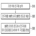
도 1은 본 발명의 한 실시예에 따른 막 구조물 제조 방법을 나타내는 개략적인 흐름도이다.
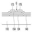
도 2는 본 발명의 다른 실시예에 따른 박막 트랜지스터를 나타내는 평면도이다.
도 3은 도 2의 절단선 Ⅲ-Ⅲ'을 따라 자른 단면도이다.
도 4는 적외선 히터를 사용하여 반도체를 열처리한 경우의 디바이스(device) 특성을 나타내는 그래프이다.
도 5는 도 2의 실시예에 따라 반도체를 열처리한 경우의 디바이스(device) 특성을 나타내는 그래프이다.
도 6은 본 발명의 또 다른 실시예에 따른 액정 표시 장치를 나타내는 단면도이다.
도 7은 도 6의 실시예에 따라 막 구조물을 형성하는 과정에서의 두께 변화를 나타내는 그래프이다.
도 8 및 도 9는 본 발명의 또 다른 실시예에 따른 액정 표시 장치의 제조 방법을 나타내는 개략도들이다.1 is a schematic flowchart illustrating a method of manufacturing a membrane structure according to an embodiment of the present invention.
2 is a plan view illustrating a thin film transistor according to another exemplary embodiment of the present invention.
3 is a cross-sectional view taken along the line III-III ′ of FIG. 2.
4 is a graph showing device characteristics when a semiconductor is heat-treated using an infrared heater.
FIG. 5 is a graph illustrating device characteristics when the semiconductor is heat treated according to the exemplary embodiment of FIG. 2.
6 is a cross-sectional view illustrating a liquid crystal display according to another exemplary embodiment of the present invention.
7 is a graph illustrating a change in thickness in the process of forming a membrane structure according to the embodiment of FIG. 6.
8 and 9 are schematic views illustrating a method of manufacturing a liquid crystal display according to still another embodiment of the present invention.
첨부한 도면들을 참조하여 본 발명의 바람직한 실시예들을 상세히 설명하기로 한다. 그러나, 본 발명은 여기서 설명되는 실시예에 한정되지 않고 다른 형태로 구체화될 수도 있다. 오히려, 여기서 소개되는 실시예들은 개시된 내용이 철저하고 완전해질 수 있도록 그리고 당업자에게 본 발명의 사상이 충분히 전달될 수 있도록 하기 위해 제공되는 것이다.Hereinafter, exemplary embodiments of the present invention will be described in detail with reference to the accompanying drawings. However, the present invention is not limited to the embodiments described herein and may be embodied in other forms. Rather, the embodiments disclosed herein are provided so that the disclosure can be thorough and complete, and will fully convey the scope of the invention to those skilled in the art.
도면들에 있어서, 층 및 영역들의 두께는 명확성을 기하기 위하여 과장된 것이다. 또한, 층이 다른 층 또는 기판 "상"에 있다고 언급되는 경우에 그것은 다른 층 또는 기판 상에 직접 형성될 수 있거나 또는 그들 사이에 제 3의 층이 개재될 수도 있다. 명세서 전체에 걸쳐서 동일한 참조번호로 표시된 부분들은 동일한 구성요소들을 의미한다.In the drawings, the thicknesses of layers and regions are exaggerated for clarity. Also, when a layer is referred to as being "on" another layer or substrate, it may be formed directly on another layer or substrate, or a third layer may be interposed therebetween. Portions denoted by like reference numerals denote like elements throughout the specification.
도 1은 본 발명의 한 실시예에 따른 막 구조물 제조 방법을 나타내는 개략적인 흐름도이다.1 is a schematic flowchart illustrating a method of manufacturing a membrane structure according to an embodiment of the present invention.
도 1을 참고하면, 기판 위에 전구체 물질을 성막한다(S10).Referring to FIG. 1, a precursor material is deposited on a substrate (S10).
상기 전구체 물질은 기판 위에 최종적으로 형성되는 막 구조물의 열처리에 의한 반응이 일어나기 전의 물질에 해당한다. 구체적으로, 상기 전구체 물질은 용매와 고형분을 포함한다.The precursor material corresponds to a material before the reaction by heat treatment of the film structure finally formed on the substrate. Specifically, the precursor material includes a solvent and a solid.
상기 전구체 물질은 스핀 코팅법, 스퍼터링법 등의 방법을 이용하여 기판 위에 형성할 수 있다.The precursor material may be formed on a substrate using a method such as spin coating or sputtering.
상기 전구체를 100℃ 내지 200℃ 온도로 예열한다(S20).The precursor is preheated to a temperature of 100 ℃ to 200 ℃ (S20).
상기 전구체를 예열하기 위해 적외선 히터를 이용하거나 광조사를 할 수 있다. 상기 광조사는 자외선 조사일 수 있다.An infrared heater may be used or light irradiation may be used to preheat the precursor. The light irradiation may be ultraviolet irradiation.
350℃ 이하의 온도에서 상기 전구체에 마이크로파(microwave)를 조사하여 막 구조물을 형성한다(S30).The precursor is microwaved at a temperature of 350 ° C. or less to form a film structure (S30).
대류식 오븐(Convection oven) 또는 노(Furnace)를 이용한 열처리의 경우, 열전달은 외부로부터 전도를 통해 이루어지게 되며, 이로 인해 기판 및 다른 구조들에도 설정 온도 또는 그 이상의 열이 가해져야만 타겟(Target)으로 하는 막(전구체)에 열이 전달된다. 따라서, 기판이 받게 되는 열 로드(thermal load)가 증가하며 가열 시간도 늘어나게 된다. 하지만, 본 발명의 실시예처럼 마이크로파를 이용할 경우 극성 분자 레벨에 열에너지가 전달되어 기판이나 다른 구조에 가해지는 열적 손실을 막을 수 있다.In the case of heat treatment using a convection oven or furnace, heat transfer is conducted through conduction from the outside, so that the substrate and other structures must be heated at a set temperature or higher to be targeted. Heat is transferred to the membrane (precursor). Thus, the thermal load the substrate receives increases and the heating time also increases. However, when the microwave is used as in the embodiment of the present invention, thermal energy is transmitted at the polar molecular level to prevent thermal loss on the substrate or other structure.
마이크로파의 흡수는 온도 의존성을 갖는다. 다시 말해, 온도가 상승함에 따라 마이크로파의 흡수는 증가한다. 이와 관련하여 본 발명의 실시예에 따르면, 마이크로파를 조사하기 이전에 상기 전구체 및 기판을 100℃ 내지 200℃ 온도로 예열함으로써 마이크로파를 조사하는 공정의 파워 손실도 줄일 수 있으며 공정 시간 단축 및 효율적인 열처리가 가능해진다.The absorption of microwaves is temperature dependent. In other words, the absorption of microwaves increases as the temperature rises. In this regard, according to an embodiment of the present invention, by preheating the precursor and the substrate to a temperature of 100 ℃ to 200 ℃ prior to the microwave irradiation, it is possible to reduce the power loss of the process of irradiating the microwave and to reduce the process time and efficient heat treatment It becomes possible.
본 발명의 실시예에 따른 막 구조물은 반도체층 또는 유기막일 수 있다. 용액 공정(졸겔법)을 이용하여 반도체층을 형성할 수 있고, 용액 공정 중에 열처리하는 과정은 본 발명의 실시예처럼 예열 후에 마이크로파 조사를 포함할 수 있다. 상기 반도체층은 산화물 반도체로 형성할 수 있다.The film structure according to the embodiment of the present invention may be a semiconductor layer or an organic film. The semiconductor layer may be formed using a solution process (sol-gel method), and the heat treatment during the solution process may include microwave irradiation after preheating as in the embodiment of the present invention. The semiconductor layer may be formed of an oxide semiconductor.
또한, 표시 장치를 형성하기 위해 다양한 막들이 형성될 수 있다. 특히 색필터, 차광막, 배향막 및 컬럼 스페이서(간격재) 등은 유기막으로 형성될 수 있는데 이러한 유기막들은 대부분 용매와 고형분(단량체)로 이루어져 있다. 이러한 유기막을 형성하기 위해 각각의 전구체 물질을 기판 위에 코팅한 후 용매의 제거 및 경화를 위해 열 또는 자외선 조사 대신에 본 발명의 실시예에 따라 예열 후에 마이크로파를 조사할 수 있다.In addition, various films may be formed to form a display device. In particular, the color filter, the light shielding film, the alignment film, and the column spacer (spacer) may be formed of an organic film, and these organic films mostly consist of a solvent and a solid (monomer). Each precursor material may be coated onto a substrate to form such an organic film and then microwaved after preheating according to an embodiment of the present invention instead of heat or ultraviolet radiation for removal and curing of the solvent.
상기 유기막을 형성하기 위한 각각의 전구체 물질은 하기의 화학식 (1) 내지 화학식 (9)로 표시한 물질일 수 있다.Each precursor material for forming the organic layer may be a material represented by the following Chemical Formulas (1) to (9).


화학식 (4)
Formula (4)


상기 화학식 (1) 내지 화학식 (9)로 표시된 물질은 음영 처리한 부분에 쌍극자(dipole)를 가진 유기재료의 분자들이다. 마이크로파의 전계가 진동(oscillation)함에 따라 쌍극자들이 동일하게 회전을 하게 된다. 이러한 쌍극자의 회전은 매우 효과적으로 재료의 가열이 가능하게 한다. 따라서, 이러한 쌍극자가 많을수록 효율적인 가열이 가능하다.The substances represented by the formulas (1) to (9) are molecules of an organic material having a dipole in the shaded portion. As the electric field of the microwave oscillates, the dipoles rotate equally. This dipole rotation makes it possible to heat the material very effectively. Therefore, the more such dipoles, the more efficient heating is possible.
도 2는 본 발명의 다른 실시예에 따른 박막 트랜지스터를 나타내는 평면도이다. 도 3은 도 2의 절단선 Ⅲ-Ⅲ'을 따라 자른 단면도이다.2 is a plan view illustrating a thin film transistor according to another exemplary embodiment of the present invention. 3 is a cross-sectional view taken along the line III-III ′ of FIG. 2.
도 2 및 도 3을 참고하면, 본 발명의 실시예에 따른 박막 트랜지스터는 절연 기판(110) 위에 게이트 전극(124)을 포함하는 게이트선(121)이 형성되어 있다. 게이트선(121)은 알루미늄 계열 금속, 은 계열 금속, 구리 계열 금속, 몰리브덴 계열 금속, 크롬(Cr), 탄탈륨(Ta) 및 티타늄(Ti) 따위로 만들어질 수 있으며, 서로 다른 두 개의 도전막을 포함하는 다중막 구조를 가질 수도 있다.2 and 3, in the thin film transistor according to the exemplary embodiment of the present invention, a
게이트선(121) 위에는 게이트 절연막(140)이 형성되어 있다.The
게이트 절연막(140) 위에는 반도체층(154)이 형성되어 있다.The
반도체층(154) 위에는 서로 마주하는 소스 전극(173) 및 드레인 전극(175)이 형성되어 있다. 박막 트랜지스터의 채널은 소스 전극(173)과 드레인 전극(175) 사이의 반도체층(154)에 형성된다.The
도 2 및 도 3에 도시한 박막 트랜지스터를 제조하는 방법에 대해 설명하면, 우선 절연 기판(110) 위에 알루미늄 계열 금속, 은 계열 금속, 구리 계열 금속, 몰리브덴 계열 금속, 크롬(Cr), 탄탈륨(Ta) 및 티타늄(Ti) 따위로 게이트 도전층을 적층하고 패터닝하여 게이트 전극(124)을 포함하는 게이트선(121)을 형성한다.Referring to the method of manufacturing the thin film transistors shown in FIGS. 2 and 3, first, an aluminum-based metal, a silver-based metal, a copper-based metal, a molybdenum-based metal, chromium (Cr), and tantalum (Ta) are disposed on the insulating substrate 110. ) And the gate conductive layer is stacked and patterned with titanium (Ti) to form a
다음, 게이트선(121) 위에 산화규소(SiOx), 질화규소(SiNx) 또는 유기 절연막 따위를 적층하여 게이트 절연막(140)을 형성한다.Next, silicon oxide (SiOx), silicon nitride (SiNx), or an organic insulating layer is stacked on the
다음, 게이트 절연막(140) 위에 앞에서 설명한 본 발명의 한 실시예에 따른 예열 및 마이크로파 조사에 의한 막 구조물 제조 방법을 이용하여 전구체 물질을 열처리하고 패터닝하여 반도체층(154)를 형성한다.Next, the
다음, 반도체층(154) 위에 도전층을 스퍼터링 등의 방법으로 적층한 후 이를 패터닝하여 소스 전극(173) 및 드레인 전극(175)을 형성한다.Next, the conductive layer is stacked on the
도 4는 적외선 히터를 사용하여 반도체를 열처리한 경우의 디바이스(device) 특성을 나타내는 그래프이다. 도 5는 도 2의 실시예에 따라 반도체를 열처리한 경우의 디바이스(device) 특성을 나타내는 그래프이다.4 is a graph showing device characteristics when a semiconductor is heat-treated using an infrared heater. FIG. 5 is a graph illustrating device characteristics when the semiconductor is heat treated according to the exemplary embodiment of FIG. 2.
도 4의 비교예는 용액 산화물 반도체를 스핀 코팅법으로 기판 위에 성막한 후 350℃ 온도로 열처리 공정을 진행하였고, 도 5의 실시예는 용액 산화물 반도체를 스핀 코팅법으로 성막한 후 적외선 히터를 사용하여 125℃로 예열한 후 마이크로파의 VFM(variable frequency microwave) 파워를 500W로 하여 표면의 온도를 350℃로 10분 동안 열처리 공정을 진행하였다.In the comparative example of FIG. 4, a solution oxide semiconductor was deposited on a substrate by spin coating, followed by a heat treatment at a temperature of 350 ° C., and the embodiment of FIG. 5 used an infrared heater after forming a solution oxide semiconductor by spin coating. After preheating to 125 ° C., the microwave was subjected to a VFM (variable frequency microwave) power of 500 W, followed by a heat treatment process at 350 ° C. for 10 minutes.
도 4 및 도 5를 참고하면, 각각 게이트 온이 될 때의 드레인 전류값(ld)을 나타낸다. 도 4 및 도 5에서 보는 바와 같이 350℃에서 예열 없이 열처리한 것보다 본 발명의 실시예와 같이 마이크로파에 의한 열처리 이전에 100℃ 내지 200℃ 온도로 예열한 경우에 게이트 온이 될 때의 드레인 전류값이 크게 상승한 것으로 비추어 볼 때, 도 5의 실시예의 경우에 디바이스(device)의 특성이 향상된 것을 알 수 있다. 또한, 도 4의 비교예의 경우 통상 400℃ 이상의 열처리를 해야 디바이스 특성을 얻을 수 있고, 350℃ 와 같이 열처리 온도가 낮을 경우 그 특성을 확보하기 어렵다.4 and 5, the drain current values ld when the gates are turned on, respectively, are shown. As shown in FIGS. 4 and 5, the drain current when the gate is turned on when preheated to a temperature of 100 ° C. to 200 ° C. prior to heat treatment by microwaves, as compared to heat treatment without preheating at 350 ° C., as shown in FIGS. In view of the large increase in the value, it can be seen that the characteristics of the device are improved in the case of the embodiment of FIG. 5. In addition, in the comparative example of FIG. 4, the device characteristics may be obtained only by heat treatment of 400 ° C. or higher, and when the heat treatment temperature is low, such as 350 ° C., it is difficult to secure the characteristics.
도 6은 본 발명의 또 다른 실시예에 따른 액정 표시 장치를 나타내는 단면도이다.6 is a cross-sectional view illustrating a liquid crystal display according to another exemplary embodiment of the present invention.
도 6을 참고하면, 본 발명의 한 실시예에 따른 액정 표시 장치는 서로 마주하는 하부 표시판(100)과 상부 표시판(200) 및 이들 두 표시판(100, 200) 사이에 위치하는 액정층(3)을 포함한다.Referring to FIG. 6, a liquid crystal display according to an exemplary embodiment of the present invention includes a
먼저, 하부 표시판(100)에 대하여 설명한다.First, the
절연 기판(110) 위에 게이트선(121) 및 유지 전극선(135)가 형성되어 있다. 게이트선(121)은 박막 트랜지스터를 구성하는 게이트 전극(124)을 포함한다.The
게이트선(121) 및 유지 전극선(135) 위에는 게이트 절연막(140)이 형성되어 있으며, 게이트 절연막(140) 위에는 반도체층(154)이 형성되어 있다. 반도체층(154)은 용액 공정(졸겔법)을 이용한 산화물 반도체로 형성할 수 있다. 반도체층(154)은 도 2 및 도 3의 실시예에서 설명한 막 구조물 제조 방법을 이용하여 형성한다.A
반도체층(154) 위에는 저항성 접촉 부재(163, 165)가 형성되어 있으며, 저항성 접촉 부재(163, 165)는 실리사이드(silicide) 또는 n형 불순물이 고농도로 도핑되어 있는 n+ 수소화 비정질 규소 따위의 물질로 만들어질 수 있다.The
저항성 접촉 부재(163, 165) 또는 게이트 절연막(140) 위에는 데이터선(171a, 171b)과 드레인 전극(175)이 형성되어 있다. 데이터선(171a, 171b)은 박막 트랜지스터를 구성하는 소스 전극(173)을 포함하며, 소스 전극(173)은 게이트 전극(124)를 중심으로 드레인 전극(175)과 마주한다.The
그러나 드레인 전극(175)을 비롯한 데이터선(171a, 171b)의 모양 및 배치는 여러 형태로 변형될 수 있다.However, the shape and arrangement of the
게이트 전극(124), 소스 전극(173) 및 드레인 전극(175)은 반도체층(154)과 함께 박막 트랜지스터(thin film transistor, TFT)를 구성한다.The
게이트 전극(124), 소스 전극(173) 및 드레인 전극(175)은 포토 공정을 통해 형성될 수 있다. 이 때, 포토 레지스트막을 이용할 수 있고, 포토 레지스트막은 유기막으로 형성할 수 있다. 포토 공정에서 포토 레지스트를 경화하여 상기 포토 레지스트막을 형성하기 위해 상기 포토 레지스트를 100℃ 내지 200℃ 온도로 예열을 한 후 350℃ 이하의 온도에서 상기 포토 레지스트에 마이크로파(microwave)를 조사하여 포토 레지스트막을 형성할 수 있다.The
데이터선(171a, 171b), 드레인 전극(175) 및 반도체층(154) 부분 위에는 질화 규소 또는 산화 규소 따위로 만들어진 하부 보호막(180p)이 형성되어 있다.A
하부 보호막(180p) 위에는 리소그라피 방법으로 형성된 색필터(230)가 형성되어 있다. 색필터(230)는 게이트선(121)과 데이터선(171a, 171b)이 교차하여 정의되는 화소 영역에 형성될 수 있고, 각 색필터(230)는 적색, 녹색 및 청색의 삼원색 등 기본색(primary color) 중 하나를 표시할 수 있다. 색필터(230)의 좌우 경계는 데이터선(171a, 171b) 위에 위치하며 데이터선(171a, 171b)을 따라 세로로 길게 뻗을 수 있다. 이 경우 색필터(230)는 띠 모양이 될 수 있다. 동일한 색의 색필터(230)는 인접하지 않을 수 있다.The
색필터(230)는 감광성 유기 조성물에 색을 구현하기 위한 안료가 포함된 구조를 가질 수 있다. 예를 들어, 색필터(230)는 감광성 유기 조성물에 적색, 녹색 또는 청색의 안료가 각각 포함된 적색, 녹색 및 청색 컬러 필터들을 포함한다.The
특히, 색필터(230)는 개구부(G1)와 그루브(G2)를 가질 수 있다. 개구부(G1)는 드레인 전극(175)과 화소 전극(191)이 접촉하는 영역에서 하부 보호막(180p)을 드러낸다. 그루브(G2)는 이웃하는 화소 영역 사이에서 서로 인접한 데이터선(171a, 171b) 사이에 형성되어 있다. 다른 실시예에서는 이웃하는 화소 영역 사이에서 서로 인접한 데이터선(171a, 171b) 사이에 서로 다른 색을 나타내는 색필터(230)가 중첩하고, 그루브(G2)가 형성되지 않는다.In particular, the
하부 보호막(180p) 및 색필터(230) 위에는 유기 물질 또는 무기 물질로 형성된 상부 보호막(180q)이 형성되어 있다. 상부 보호막(180q)은 색필터(230)를 보호하는 동시에 하단에 형성된 층들을 평탄화 역할을 할 수 있다.An upper passivation layer 180q formed of an organic material or an inorganic material is formed on the
색필터(230)는 용매와 고형분으로 이루어진 전구체를 경화하여 형성될 수 있다. 상기 전구체를 경화하기 위해 100℃ 내지 200℃ 온도로 예열을 한 후 350℃ 이하의 온도에서 상기 전구체에 마이크로파(microwave)를 조사하여 색필터(230)를 형성할 수 있다.The
상부 보호막(180q)은 드레인 전극(175)을 노출하는 접촉 구멍(185)을 갖는다. 접촉 구멍(185)은 색필터(230)가 갖는 개구부(G1)와 연결되어 중첩하고 있다.The upper passivation layer 180q has a
상부 보호막(180q) 위에는 화소 전극(191)이 형성되어 있다. 화소 전극(191)은 ITO 또는 IZO 등의 투명한 도전 물질이나 알루미늄, 은, 크롬 또는 그 합금 등의 반사성 금속으로 만들어질 수 있다.The
상부 보호막(180q) 위에 차광 부재(220), 화소 전극(191) 위에 간격재(363M)가 형성되어 있다. 차광 부재(220)는 화소 영역의 경계와 박막 트랜지스터에 대응하는 부분에 형성한다. 하지만, 화소 전극(191)과 드레인 전극(175)이 접촉하는 접촉 구멍(185)에는 차광 부재(220)가 아닌 간격재(363M)가 형성되어 있다.The
간격재(363M)는 접촉 구멍(185)을 채우며, 상부 표시판(200)을 향해 돌출되어 있다. 간격재(363M)는 상부 표시판(200)과 하부 표시판(100) 사이의 간격을 유지하는 역할을 한다. 간격재(363M)는 상부 표시판(200)과 접촉할 수 있다.The
차광 부재(220)와 간격재(363M)는 동시에 형성될 수 있고, 착색 유기막과 같은 물질로 형성될 수 있다.The
차광 부재(220)는 간격재(363M)보다 낮은 높이로 형성된다.The
다음, 상부 표시판(200)에 대해서 설명한다.Next, the
상부 표시판(200)은 투명한 절연 기판(210) 위에 공통 전극(270)이 전면에 형성되어 있고, 공통 전극(270) 위에 배향막(미도시)이 형성되어 있다. 상기 배향막은 폴리 이미드로 형성할 수 있다.In the
상기 배향막은 도 1의 실시예에서 설명한 것처럼 배향막 전구체를 공통 전극(270) 위에 성막하고, 상기 배향막 전구체를 100℃ 내지 200℃ 온도로 예열한 후 350℃ 이하의 온도에서 상기 배향막 전구체에 마이크로파(microwave)를 조사하여 상기 배향막을 형성할 수 있다.As described in the embodiment of FIG. 1, the alignment layer is formed by depositing an alignment layer precursor on the
이상에서 설명한 간격재(363M), 차광 부재(220)는 유기막으로 형성될 수 있다. 이러한 유기막을 형성하기 위해 각각의 전구체 물질을 기판 위에 코팅한 후 용매의 제거 및 경화를 위해 열 또는 자외선 조사 대신에 도 1의 실시예에 따라 예열 후에 마이크로파를 조사할 수 있다.The
이상에서 설명한 실시예에서는 차광 부재(220)가 하부 표시판(100)에형성되지만, 이와 달리 상부 표시판(200) 위에 차광 부재를 형성할 수 있다. 상부 표시판(200) 위에 차광 부재를 형성하는 실시예를 간략히 설명하면 다음과 같다.In the exemplary embodiment described above, the
절연 기판(210) 위에 화소 영역의 경계와 박막 트랜지스터에 대응하는 부분에 차광 부재를 형성할 수 있다. 상기 차광 부재 위에 막의 평탄화를 위해 오버 코트층을 형성할 수 있다. 상기 오버 코트층 위에 공통 전극을 형성할 수 있다. 오버 코트층은 유기막으로 형성할 수 있고, 이러한 유기막을 형성하기 위해 오버 코트층의 전구체 물질을 기판 위에 코팅한 후 용매의 제거 및 경화를 위해 열 또는 자외선 조사 대신에 도 1의 실시예에 따라 예열 후에 마이크로파를 조사할 수 있다.A light blocking member may be formed on the insulating
도 7은 도 6의 실시예에 따라 막 구조물을 형성하는 과정에서의 두께 변화를 나타내는 그래프이다.7 is a graph illustrating a change in thickness in the process of forming a membrane structure according to the embodiment of FIG. 6.
도 7은 구체적으로 적색 색필터(red), 녹색 색필터(green), 청색 색필터(blue), 차광막(유기 BM), 본 발명의 실시예에서 설명한 간격재에 대응하는 컬럼 스페이서(CS)에 마이크로파를 조사하는 시간에 따른 두께 변화를 나타낸다. 차광막, 컬럼 스페이서는 두께 변화가 거의 없고, 색필터의 경우에는 미세한 두께 변화가 존재하나 오차 범위 이내 수준이다.7 illustrates a red, green, blue, blue, light-shielding (organic BM), and column spacer (CS) corresponding to the spacer described in the embodiment of the present invention. The thickness change with time of microwave irradiation is shown. The light shielding film and the column spacer have almost no thickness change, and in the case of the color filter, there is a slight thickness change but is within an error range.
결과적으로 마이크로파를 조사하여 유기막 구조물을 형성하는 경우에 균일한 두께의 막을 형성할 수 있음을 알 수 있다.As a result, it can be seen that a film having a uniform thickness can be formed when the organic film structure is formed by irradiating microwaves.
도 8 및 도 9는 본 발명의 또 다른 실시예에 따른 액정 표시 장치의 제조 방법을 나타내는 개략도들이다.8 and 9 are schematic views illustrating a method of manufacturing a liquid crystal display according to still another embodiment of the present invention.
구체적으로, 도 8 및 도 9는 배향 보조제에 의해 액정의 선경사를 형성하는 방법을 나타낸다.Specifically, FIGS. 8 and 9 show a method of forming the pretilt of the liquid crystal by the alignment aid.
도 8 및 도 9를 참고하면, 화소 전극(191)과 공통 전극(270) 사이에 배향 보조제(50) 및 액정 분자(310)를 포함하는 액정층이 위치한다. 화소 전극(191)과 공통 전극(270) 위에는 배향 물질을 도포하여 형성된 배향막(11, 21)이 위치하고 있다.8 and 9, a liquid crystal layer including an
배향막(11, 21)은 폴리 아믹산(Polyamic acid), 폴리실록산(Polysiloxane) 또는 폴리 이미드(Polyimide) 등의 액정 배향막으로써 일반적으로 사용되는 물질들 중 적어도 하나를 포함하여 형성될 수 있다.The alignment layers 11 and 21 may include at least one of materials generally used as liquid crystal alignment layers such as polyamic acid, polysiloxane, or polyimide.
액정 분자(310)는 전압을 인가하지 않았을 때 화소 전극(191) 및 공통 전극(270)에 대해 수직인 방향으로 배열되어 있다.The
이 때, 화소 전극(191)과 공통 전극(270)에 전압을 인가한다. 전압 인가에 의해 액정 분자(310) 및 배향 보조제(50)는 경사각을 가지면서 기울어진다.In this case, a voltage is applied to the
이와 같이 화소 전극(191)과 공통 전극(270) 사이에 전압이 인가된 상태에서 100℃ 내지 200℃ 온도로 배향 보조제(50) 및 액정 분자(310)를 포함하는 액정층을 예열한다. 이후에 350℃ 이하의 온도에서 상기 액정층에 마이크로파(microwave)를 조사하여 배향 보조제(50)를 중합시킨다. 배향 보조제(50)는 반응성 메소겐(Reactive mesogen; RM)으로 표현될 수 있다.As described above, the liquid crystal layer including the
이상에서 본 발명의 바람직한 실시예에 대하여 상세하게 설명하였지만 본 발명의 권리범위는 이에 한정되는 것은 아니고 다음의 청구범위에서 정의하고 있는 본 발명의 기본 개념을 이용한 당업자의 여러 변형 및 개량 형태 또한 본 발명의 권리범위에 속하는 것이다.
While the present invention has been particularly shown and described with reference to exemplary embodiments thereof, it is to be understood that the invention is not limited to the disclosed exemplary embodiments, Of the right.
11, 12배향막50배향 보조제
110, 210 절연 기판 154반도체
173소스 전극175드레인 전극
191화소 전극270공통 전극
310액정 분자11, 12
110, 210
191
310 liquid crystal molecules
Claims (20)
Translated fromKorean상기 전구체를 예열하는 단계 그리고
상기 전구체에 마이크로파(microwave)를 조사하여 막 구조물을 형성하는 단계를 포함하는 막 구조물 제조 방법.
Forming a precursor on the substrate,
Preheating the precursor and
Irradiating microwave to the precursor to form a film structure.
상기 전구체를 예열하는 단계는 100℃ 내지 200℃의 온도로 수행하는 막 구조물 제조 방법.
In claim 1,
Preheating the precursor is a film structure manufacturing method performed at a temperature of 100 ℃ to 200 ℃.
상기 전구체를 예열하는 단계는 적외선 히터를 이용하거나 광조사하는 것을 포함하는 막 구조물 제조 방법.
In claim 2,
Preheating the precursor comprises using an infrared heater or irradiating light.
상기 전구체에 마이크로파를 조사하는 단계는 350℃ 이하의 온도에서 수행하는 막 구조물 제조 방법.
4. The method of claim 3,
Irradiating the microwave to the precursor is a film structure manufacturing method performed at a temperature of 350 ℃ or less.
상기 전구체에 마이크로파를 조사하는 단계에서 상기 마이크로파는 300MHz 내지 300GHz의 주파수 범위를 갖도록 하는 막 구조물 제조 방법.
In claim 4,
And irradiating the precursor with microwaves such that the microwaves have a frequency range of 300 MHz to 300 GHz.
상기 막 구조물은 용액 공정을 이용한 반도체로 형성되는 막 구조물 제조 방법.
In claim 1,
The film structure is a film structure manufacturing method of forming a semiconductor using a solution process.
상기 막 구조물은 유기막으로 형성되는 막 구조물 제조 방법.
In claim 1,
The membrane structure manufacturing method of the membrane structure is formed of an organic layer.
상기 유기막은 색필터, 차광막, 배향막, 포토 레지스트막, 컬럼 스페이서, 오버코트층 및 간격재 중 적어도 하나로 형성되는 막 구조물 제조 방법.
In claim 7,
And the organic film is formed of at least one of a color filter, a light shielding film, an alignment film, a photoresist film, a column spacer, an overcoat layer, and a spacer.
상기 유기막은 쌍극자(dipole)를 포함하는 유기 물질로 형성되는 막 구조물 제조 방법.
In claim 7,
And the organic film is formed of an organic material including a dipole.
상기 유기막은 폴리 스티렌(Poly-styrene), 메틸 메타아크릴레이트(Methyl Methacrylate), 메타크릴산(Methacrylic acid), 하이드록시에틸 메타아크릴레이트(Hydroxyethyl methacrylate), 3-에톡시프로판산 에틸(Ethyl 3-Ethoxypropionate), 프로필렌글리콜-모노에틸에테르 (Propyleneglycol-monoethylether), 사이클로헥사논 (Cyclohexanone), 프로필렌글리콜 모노메틸에테르아세테이트 (PGMEA), 폴리이미드(Polyimide) 중 하나인 막 구조물 제조 방법.
In claim 9,
The organic layer may be made of polystyrene, methyl methacrylate, methacrylic acid, hydroxyethyl methacrylate, ethyl 3-ethoxypropane. Method of producing a membrane structure which is one of Ethoxypropionate, Propyleneglycol-monoethylether, Cyclohexanone, Propylene glycol monomethyl ether acetate (PGMEA), Polyimide.
상기 전기장 생성 전극 위에 배향막을 형성하는 단계,
상기 제1 기판과 상기 제2 기판 사이에 액정 및 배향 보조제를 포함하는 액정층을 형성하는 단계 그리고
상기 배향막과 상기 액정층에 마이크로파를 조사하여 배향 중합체를 형성하는 단계를 포함하는 액정 표시 장치의 제조 방법.
Forming an electric field generating electrode on at least one of a first substrate and a second substrate facing the first substrate,
Forming an alignment layer on the field generating electrode;
Forming a liquid crystal layer comprising a liquid crystal and an alignment aid between the first substrate and the second substrate, and
And irradiating microwaves to the alignment layer and the liquid crystal layer to form an alignment polymer.
상기 배향 중합체를 형성하는 단계 이전에 상기 배향막과 상기 액정층을 예열하는 단계를 더 포함하는 액정 표시 장치의 제조 방법.
In claim 11,
And preheating the alignment layer and the liquid crystal layer prior to the forming of the alignment polymer.
상기 배향막과 상기 액정층을 예열하는 단계는 100℃ 내지 200℃의 온도로 수행하는 액정 표시 장치의 제조 방법.
In claim 12,
The pre-heating of the alignment layer and the liquid crystal layer is carried out at a temperature of 100 ℃ to 200 ℃ manufacturing method of a liquid crystal display device.
상기 배향막과 상기 액정층에 마이크로파를 조사하는 단계는 350℃ 이하의 온도에서 수행하는 액정 표시 장치의 제조 방법.
In claim 13,
Irradiating microwaves to the alignment layer and the liquid crystal layer is performed at a temperature of 350 ℃ or less.
상기 배향막과 상기 액정층에 마이크로파를 조사하는 단계에서 상기 마이크로파는 300MHz 내지 300GHz의 주파수 범위를 갖도록 하는 액정 표시 장치의 제조 방법.
The method of claim 14,
And irradiating microwaves to the alignment layer and the liquid crystal layer so that the microwaves have a frequency range of 300 MHz to 300 GHz.
상기 게이트선 위에 게이트 절연막을 형성하는 단계,
상기 게이트 절연막 위에 전구체를 형성하는 단계,
상기 전구체를 예열하는 단계,
상기 예열된 전구체에 마이크로파를 조사하여 반도체층을 형성하는 단계 그리고
상기 반도체층 위에 서로 마주하도록 소스 전극 및 드레인 전극을 형성하는 단계를 포함하는 박막 트랜지스터의 제조 방법.
Forming a gate line on the substrate,
Forming a gate insulating film on the gate line;
Forming a precursor on the gate insulating film,
Preheating the precursor,
Irradiating microwaves to the preheated precursor to form a semiconductor layer;
Forming a source electrode and a drain electrode to face each other on the semiconductor layer.
상기 전구체를 예열하는 단계는 적외선 히터를 이용하거나 광조사하는 것을 포함하는 박막 트랜지스터의 제조 방법.
The method of claim 16,
Preheating the precursor comprises using an infrared heater or irradiating light.
상기 전구체에 마이크로파를 조사하는 단계는 350℃ 이하의 온도에서 수행하는 박막 트랜지스터의 제조 방법.
The method of claim 17,
Irradiating the microwave to the precursor is a method of manufacturing a thin film transistor is carried out at a temperature of 350 ℃ or less.
상기 전구체에 마이크로파를 조사하는 단계에서 상기 마이크로파는 300MHz 내지 300GHz의 주파수 범위를 갖도록 하는 박막 트랜지스터의 제조 방법.
The method of claim 18,
And irradiating microwaves to the precursors such that the microwaves have a frequency range of 300 MHz to 300 GHz.
상기 반도체층은 용액 공정을 이용한 산화물 반도체로 형성되는 박막 트랜지스터의 제조 방법.
The method of claim 16,
And the semiconductor layer is formed of an oxide semiconductor using a solution process.
Priority Applications (2)
| Application Number | Priority Date | Filing Date | Title |
|---|---|---|---|
| KR1020100103074AKR20120041568A (en) | 2010-10-21 | 2010-10-21 | Method for manufacturing a film structure |
| US13/100,149US20120100649A1 (en) | 2010-10-21 | 2011-05-03 | Method for manufacturing a film structure |
Applications Claiming Priority (1)
| Application Number | Priority Date | Filing Date | Title |
|---|---|---|---|
| KR1020100103074AKR20120041568A (en) | 2010-10-21 | 2010-10-21 | Method for manufacturing a film structure |
Publications (1)
| Publication Number | Publication Date |
|---|---|
| KR20120041568Atrue KR20120041568A (en) | 2012-05-02 |
Family
ID=45973357
Family Applications (1)
| Application Number | Title | Priority Date | Filing Date |
|---|---|---|---|
| KR1020100103074AWithdrawnKR20120041568A (en) | 2010-10-21 | 2010-10-21 | Method for manufacturing a film structure |
Country Status (2)
| Country | Link |
|---|---|
| US (1) | US20120100649A1 (en) |
| KR (1) | KR20120041568A (en) |
Families Citing this family (1)
| Publication number | Priority date | Publication date | Assignee | Title |
|---|---|---|---|---|
| US10224258B2 (en)* | 2013-03-22 | 2019-03-05 | Applied Materials, Inc. | Method of curing thermoplastics with microwave energy |
Family Cites Families (1)
| Publication number | Priority date | Publication date | Assignee | Title |
|---|---|---|---|---|
| JP5644111B2 (en)* | 2007-12-26 | 2014-12-24 | コニカミノルタ株式会社 | METAL OXIDE SEMICONDUCTOR AND ITS MANUFACTURING METHOD, SEMICONDUCTOR ELEMENT, THIN FILM TRANSISTOR |
- 2010
- 2010-10-21KRKR1020100103074Apatent/KR20120041568A/ennot_activeWithdrawn
- 2011
- 2011-05-03USUS13/100,149patent/US20120100649A1/ennot_activeAbandoned
Also Published As
| Publication number | Publication date |
|---|---|
| US20120100649A1 (en) | 2012-04-26 |
Similar Documents
| Publication | Publication Date | Title |
|---|---|---|
| US12072581B2 (en) | Liquid crystal display device and manufacturing method thereof | |
| JP3911929B2 (en) | Manufacturing method of liquid crystal display device | |
| JP4290905B2 (en) | Organic film planarization method | |
| KR101799528B1 (en) | Black matrix material for off-set printing apparatus and method of fabricating color filter substrate using the same | |
| KR20100026202A (en) | Liquid crystal display device and the manufacturing method thereof | |
| KR101473792B1 (en) | Liquid crystal display device manufacturing method and liquid crystal display device therefor | |
| US20160041441A1 (en) | Display panel and method for manufacturing the same | |
| KR101281756B1 (en) | Method for manufacturing liquid crystal display device and liquid crystal display device manufactured using the same | |
| JP5889704B2 (en) | Manufacturing method of liquid crystal display device | |
| KR20120041568A (en) | Method for manufacturing a film structure | |
| WO2012086159A1 (en) | Display device, thin-film transistor substrate, and method for producing same | |
| KR102282217B1 (en) | Liquid crystal display and method of manufacturing the same | |
| KR20090051824A (en) | LCD and its manufacturing method | |
| US9134573B2 (en) | Method of producing photo-alignment layer of liquid crystal display | |
| KR101467215B1 (en) | Liquid crystal disply device having in cell retardation film and method for fabricating the same | |
| KR20070025447A (en) | Liquid Crystal Display and Manufacturing Method Thereof | |
| KR20130057594A (en) | Method of fabricating array substrate for in-plane switching mode liquid crystal display device | |
| JPS59172627A (en) | Display panel | |
| JP3924992B2 (en) | Color filter and electro-optical device including the color filter | |
| JP4156343B2 (en) | Method for manufacturing substrate for liquid crystal display device and method for manufacturing liquid crystal display device using the same | |
| KR101030532B1 (en) | Manufacturing Method of TFT Array Substrate | |
| KR20070070403A (en) | Liquid crystal display device and manufacturing method thereof | |
| CN1437055A (en) | Liquid crystal display plate with reflective electrode and producing method thereof | |
| WO2019116745A1 (en) | Liquid crystal display device and method of manufacture therefor | |
| JP2000066242A (en) | Liquid crystal electro-optical device |
Legal Events
| Date | Code | Title | Description |
|---|---|---|---|
| PA0109 | Patent application | Patent event code:PA01091R01D Comment text:Patent Application Patent event date:20101021 | |
| PG1501 | Laying open of application | ||
| N231 | Notification of change of applicant | ||
| PN2301 | Change of applicant | Patent event date:20120913 Comment text:Notification of Change of Applicant Patent event code:PN23011R01D | |
| PC1203 | Withdrawal of no request for examination | ||
| WITN | Application deemed withdrawn, e.g. because no request for examination was filed or no examination fee was paid |