KR20120029291A - Semiconductor devices and methods of fabricating the same - Google Patents
Semiconductor devices and methods of fabricating the sameDownload PDFInfo
- Publication number
- KR20120029291A KR20120029291AKR1020100091300AKR20100091300AKR20120029291AKR 20120029291 AKR20120029291 AKR 20120029291AKR 1020100091300 AKR1020100091300 AKR 1020100091300AKR 20100091300 AKR20100091300 AKR 20100091300AKR 20120029291 AKR20120029291 AKR 20120029291A
- Authority
- KR
- South Korea
- Prior art keywords
- pattern
- patterns
- gap fill
- semiconductor
- gapfill
- Prior art date
- Legal status (The legal status is an assumption and is not a legal conclusion. Google has not performed a legal analysis and makes no representation as to the accuracy of the status listed.)
- Withdrawn
Links
Images


Classifications
- H—ELECTRICITY
- H10—SEMICONDUCTOR DEVICES; ELECTRIC SOLID-STATE DEVICES NOT OTHERWISE PROVIDED FOR
- H10B—ELECTRONIC MEMORY DEVICES
- H10B43/00—EEPROM devices comprising charge-trapping gate insulators
- H10B43/20—EEPROM devices comprising charge-trapping gate insulators characterised by three-dimensional arrangements, e.g. with cells on different height levels
- H10B43/23—EEPROM devices comprising charge-trapping gate insulators characterised by three-dimensional arrangements, e.g. with cells on different height levels with source and drain on different levels, e.g. with sloping channels
- H10B43/27—EEPROM devices comprising charge-trapping gate insulators characterised by three-dimensional arrangements, e.g. with cells on different height levels with source and drain on different levels, e.g. with sloping channels the channels comprising vertical portions, e.g. U-shaped channels
- H—ELECTRICITY
- H10—SEMICONDUCTOR DEVICES; ELECTRIC SOLID-STATE DEVICES NOT OTHERWISE PROVIDED FOR
- H10D—INORGANIC ELECTRIC SEMICONDUCTOR DEVICES
- H10D30/00—Field-effect transistors [FET]
- H10D30/60—Insulated-gate field-effect transistors [IGFET]
- H10D30/69—IGFETs having charge trapping gate insulators, e.g. MNOS transistors
- H10D30/693—Vertical IGFETs having charge trapping gate insulators
- H—ELECTRICITY
- H10—SEMICONDUCTOR DEVICES; ELECTRIC SOLID-STATE DEVICES NOT OTHERWISE PROVIDED FOR
- H10D—INORGANIC ELECTRIC SEMICONDUCTOR DEVICES
- H10D84/00—Integrated devices formed in or on semiconductor substrates that comprise only semiconducting layers, e.g. on Si wafers or on GaAs-on-Si wafers
- H10D84/01—Manufacture or treatment
- H10D84/0123—Integrating together multiple components covered by H10D12/00 or H10D30/00, e.g. integrating multiple IGBTs
- H10D84/0126—Integrating together multiple components covered by H10D12/00 or H10D30/00, e.g. integrating multiple IGBTs the components including insulated gates, e.g. IGFETs
- H10D84/0149—Manufacturing their interconnections or electrodes, e.g. source or drain electrodes
- H—ELECTRICITY
- H10—SEMICONDUCTOR DEVICES; ELECTRIC SOLID-STATE DEVICES NOT OTHERWISE PROVIDED FOR
- H10D—INORGANIC ELECTRIC SEMICONDUCTOR DEVICES
- H10D84/00—Integrated devices formed in or on semiconductor substrates that comprise only semiconducting layers, e.g. on Si wafers or on GaAs-on-Si wafers
- H10D84/01—Manufacture or treatment
- H10D84/0123—Integrating together multiple components covered by H10D12/00 or H10D30/00, e.g. integrating multiple IGBTs
- H10D84/0126—Integrating together multiple components covered by H10D12/00 or H10D30/00, e.g. integrating multiple IGBTs the components including insulated gates, e.g. IGFETs
- H10D84/016—Integrating together multiple components covered by H10D12/00 or H10D30/00, e.g. integrating multiple IGBTs the components including insulated gates, e.g. IGFETs the components including vertical IGFETs
- H—ELECTRICITY
- H10—SEMICONDUCTOR DEVICES; ELECTRIC SOLID-STATE DEVICES NOT OTHERWISE PROVIDED FOR
- H10D—INORGANIC ELECTRIC SEMICONDUCTOR DEVICES
- H10D88/00—Three-dimensional [3D] integrated devices
Landscapes
- Semiconductor Memories (AREA)
- Non-Volatile Memory (AREA)
Abstract
Translated fromKoreanDescription
Translated fromKorean본 발명은 반도체 소자 및 그 제조 방법에 관한 것이다.The present invention relates to a semiconductor device and a method of manufacturing the same.
반도체 소자를 구성하는 요소들이 차지하는 평면적을 줄이기 위한 연구가 진행되고 있다.Research is underway to reduce the planar area occupied by elements constituting semiconductor devices.
본 발명이 해결하고자 하는 기술적 과제는 제1 결정질 실리콘으로 이루어진 반도체 패턴과 제2 결정질 실리콘으로 이루어진 패드 패턴이 안정적으로 접촉을 할 수 있는 반도체 소자의 구조를 제공하는데 있다.The present invention has been made in an effort to provide a structure of a semiconductor device in which a semiconductor pattern made of first crystalline silicon and a pad pattern made of second crystalline silicon can be stably contacted.
본 발명이 해결하고자 하는 기술적 과제는 결정질 실리콘으로 이루어진 막들에 의해 상부, 하부 및 측벽이 덮이며 내부에 보이드(void)가 없는 갭필 구조체를 포함하는 반도체 소자를 제공하는데 있다.SUMMARY The present invention has been made in an effort to provide a semiconductor device including a gapfill structure in which tops, bottoms, and sidewalls are covered by films made of crystalline silicon, and voids are not formed therein.
본 발명이 해결하고자 하는 또 다른 기술적 과제는 채널 영역으로 이용되는 반도체 패턴의 특성 열화를 방지할 수 있는 방법에 의해 제조된 반도체 소자를 제공하는데 있다.Another technical problem to be solved by the present invention is to provide a semiconductor device manufactured by a method capable of preventing the deterioration of characteristics of the semiconductor pattern used as the channel region.
본 발명이 해결하고자 하는 과제들은 이상에서 언급한 과제로 제한되지 않으며, 언급되지 않은 또 다른 과제들은 아래의 기재로부터 당 업자에게 명확하게 이해될 수 있을 것이다.Problems to be solved by the present invention are not limited to the above-mentioned problems, and other tasks not mentioned will be clearly understood by those skilled in the art from the following description.
본 발명의 일 양태에 따르면, 패드 패턴과 반도체 패턴을 갖는 반도체 소자를 제공한다. 이 소자는 기판 상에 제공되며 하나 또는 복수의 개구부를 갖는 수평 패턴들을 포함한다. 상기 개구부의 상부 영역 내에 패드 패턴이 제공된다. 상기 패드 패턴과 상기 기판 사이의 상기 개구부 내에 절연성의 갭필 구조체가 제공된다. 상기 갭필 구조체는 제1 산화물을 포함하는 제1 갭필 패턴 및 상기 제1 산화물과 다른 식각 선택비를 갖는 제2 갭필 패턴들을 포함한다.According to one aspect of the present invention, a semiconductor device having a pad pattern and a semiconductor pattern is provided. The device includes horizontal patterns provided on a substrate and having one or a plurality of openings. A pad pattern is provided in the upper region of the opening. An insulating gapfill structure is provided in the opening between the pad pattern and the substrate. The gapfill structure may include a first gapfill pattern including a first oxide and second gapfill patterns having an etching selectivity different from that of the first oxide.
상기 수평 패턴들의 측벽들과 상기 갭필 구조체의 측벽과 상기 수평 패턴들의 측벽들 사이 및 상기 패드 패턴과 상기 수평 패턴들의 측벽들 사이에 반도체 패턴이 제공된다.A semiconductor pattern is provided between sidewalls of the horizontal patterns, sidewalls of the gapfill structure and sidewalls of the horizontal patterns, and between the pad pattern and sidewalls of the horizontal patterns.
몇몇 실시예들에서, 상기 반도체 패턴으로부터 연장되어 상기 갭필 구조체와 상기 기판 사이에 개재된 반도체 패턴의 바닥 부(bottom portion)를 더 포함할 수 있다.In some embodiments, the semiconductor device may further include a bottom portion of the semiconductor pattern extending from the semiconductor pattern and interposed between the gap fill structure and the substrate.
다른 실시예에서, 상기 제1 및 제2 갭필 패턴들은 서로 다른 불순물을 함유한 실리콘 산화물을 포함할 수 있다. 여기서, 상기 제1 갭필 패턴은 수소 원소 및 염소 원소를 함유하는 실리콘 산화물을 포함하고, 상기 제2 갭필 패턴은 질소 원소, 수소 원소 및 탄소 원소 중 적어도 하나를 포함하는 실리콘 산화물을 포함할 수 있다.In another embodiment, the first and second gapfill patterns may include silicon oxide containing different impurities. Here, the first gap fill pattern may include silicon oxide containing a hydrogen element and a chlorine element, and the second gap fill pattern may include a silicon oxide including at least one of a nitrogen element, a hydrogen element, and a carbon element.
또 다른 실시예에서, 상기 제1 갭필 패턴은 상부면의 가운데 부분이 오목하게 함몰된 모양이고, 상기 제2 갭필 패턴은 상기 제1 갭필 패턴과 상기 패드 패턴 사이에 개재될 수 있다.In another embodiment, the first gap fill pattern may have a shape in which a center portion of the upper surface is concave, and the second gap fill pattern may be interposed between the first gap fill pattern and the pad pattern.
또 다른 실시예에서, 상기 제2 갭필 패턴은 기둥 모양이고, 상기 제1 갭필 패턴은 상기 제2 갭필 패턴의 측벽을 둘러싸도록 형성될 수 있다.In another embodiment, the second gapfill pattern may have a pillar shape, and the first gapfill pattern may be formed to surround sidewalls of the second gapfill pattern.
또 다른 실시예에서, 상기 제1 갭필 패턴은 상부면의 가운데 부분이 상기 개구부의 중간 또는 하부 영역까지 함몰된 모양이고, 상기 제2 갭필 패턴은 상기 제1 갭필 패턴과 상기 패드 패턴 사이에 개재될 수 있다.In another embodiment, the first gap fill pattern may have a shape in which a center portion of an upper surface of the first gap fill pattern is recessed to a middle or lower region of the opening, and the second gap fill pattern may be interposed between the first gap fill pattern and the pad pattern. Can be.
또 다른 실시예에서, 상기 개구부는 홀 형상일 수 있다.In another embodiment, the opening may have a hole shape.
또 다른 실시예에서, 상기 개구부는, 평면에서, 라인 형상으로써 상기 수평 패턴들을 가로지를 수 있다.In another embodiment, the opening may cross the horizontal patterns in a line shape in a plane.
또 다른 실시예에서, 상기 수평 패턴들은 복수의 도전성 패턴들과 복수의 절연 패턴들이 교대로 적층되어 형성되되, 상기 수평 패턴들의 최상층은 절연 패턴이고, 상기 도전성 패턴들 중 최하부에 위치한 도전성 패턴은 상기 기판과 이격될 수 있다.In another embodiment, the horizontal patterns are formed by alternately stacking a plurality of conductive patterns and a plurality of insulating patterns, wherein the uppermost layer of the horizontal patterns is an insulating pattern, and the conductive patterns positioned at the lowermost of the conductive patterns are the It may be spaced apart from the substrate.
또한, 상기 제1 갭필 패턴은 상기 도전성 패턴들과 인접하는 상기 반도체 패턴을 덮을 수 있다.In addition, the first gap fill pattern may cover the semiconductor pattern adjacent to the conductive patterns.
또한, 상기 도전성 패턴들과 상기 반도체 패턴 사이에 개재된 게이트 절연막을 더 포함할 수 있다.The gate insulating layer may further include a gate insulating layer interposed between the conductive patterns and the semiconductor pattern.
또한, 상기 게이트 절연막은 상기 도전성 패턴들과 상기 절연 패턴들 사이로 연장될 수 있다.In addition, the gate insulating layer may extend between the conductive patterns and the insulating patterns.
또한, 상기 게이트 절연막은 상기 반도체 패턴과 상기 도전성 패턴들 사이에 개재됨과 아울러, 상기 반도체 패턴과 상기 절연 패턴들 사이에 개재될 수 있다.The gate insulating layer may be interposed between the semiconductor pattern and the conductive patterns and may be interposed between the semiconductor pattern and the insulating patterns.
또한, 상기 반도체 패턴은 트랜지스터의 채널 영역으로 정의되고, 상기 게이트 절연막은 비휘발성 메모리 셀의 정보 저장을 위한 막을 포함하고, 상기 도전성 패턴들은 게이트 전극들로 정의될 수 있다.In addition, the semiconductor pattern may be defined as a channel region of a transistor, the gate insulating layer may include a film for storing information of a nonvolatile memory cell, and the conductive patterns may be defined as gate electrodes.
또 다른 실시예에서, 상기 반도체 패턴은 결정질 실리콘을 포함하고, 상기 패드 패턴은 폴리 실리콘을 포함할 수 있다.
In another embodiment, the semiconductor pattern may include crystalline silicon, and the pad pattern may include polysilicon.
본 발명의 또 다른 양태에 따르면, 갭필 구조체를 갖는 반도체 소자를 제공한다. 이 소자는 반도체 기판 상에 제공된 수평 패턴들을 포함한다. 상기 수평 패턴들은 교대로 적층된 게이트 전극들 및 절연 패턴들을 포함한다. 상기 수평 패턴들을 관통하며 상기 기판을 노출시키는 하나 또는 복수의 개구부가 제공된다. 상기 개구부의 상부 영역 내에 결정질 실리콘을 포함하는 패드 패턴이 제공된다. 상기 패드 패턴과 상기 반도체 기판 사이의 상기 개구부 내에 갭필 구조체가 제공된다. 상기 갭필 구조체는 제1 산화물을 포함하는 제1 갭필 패턴 및 상기 제1 산화물과 다른 식각 선택비를 갖는 제2 산화물을 포함한다. 상기 갭필 구조체의 측벽과 상기 수평 패턴들의 측벽들 사이 및 상기 패드 패턴과 상기 수평 패턴들의 측벽들 사이에 형성되며, 결정질 실리콘을 포함하는 반도체 패턴이 제공된다. 상기 패드 패턴 및 상기 패드 패턴과 인접하는 상기 반도체 패턴 내에 불순물 영역이 제공된다. 상기 반도체 패턴과 상기 게이트 전극들 사이에 정보 저장 막을 갖는 게이트 절연막이 제공된다.According to still another aspect of the present invention, a semiconductor device having a gapfill structure is provided. This device includes horizontal patterns provided on a semiconductor substrate. The horizontal patterns include gate electrodes and insulating patterns that are alternately stacked. One or a plurality of openings are provided through the horizontal patterns to expose the substrate. A pad pattern including crystalline silicon is provided in an upper region of the opening. A gapfill structure is provided in the opening between the pad pattern and the semiconductor substrate. The gapfill structure includes a first gapfill pattern including a first oxide and a second oxide having an etching selectivity different from that of the first oxide. A semiconductor pattern is formed between the sidewalls of the gapfill structure and the sidewalls of the horizontal patterns and between the pad pattern and the sidewalls of the horizontal patterns and includes crystalline silicon. An impurity region is provided in the pad pattern and the semiconductor pattern adjacent to the pad pattern. A gate insulating film having an information storage film is provided between the semiconductor pattern and the gate electrodes.
몇몇 실시예들에서, 상기 반도체 패턴으로부터 연장되어 상기 갭필 구조체와 상기 기판 사이에 개재된 반도체 패턴의 바닥부(bottom portion)를 더 포함할 수 있다.In some embodiments, the semiconductor device may further include a bottom portion of the semiconductor pattern extending from the semiconductor pattern and interposed between the gap fill structure and the substrate.
다른 실시예에서, 상기 개구부 내에서, 상기 도전성 패턴들의 측벽들은 상기 절연성 패턴들의 측벽들과 수직 정렬 되지 않을 수 있다.In another embodiment, within the opening, sidewalls of the conductive patterns may not be vertically aligned with sidewalls of the insulating patterns.
또 다른 실시예에서, 상기 개구부 내에서, 상기 도전성 패턴들의 측벽들은 상기 절연성 패턴들의 측벽들과 수직 정렬될 수 있다.
In another embodiment, within the opening, sidewalls of the conductive patterns may be vertically aligned with sidewalls of the insulating patterns.
본 발명의 또 다른 양태에 따르면, 채널 영역으로 이용되는 반도체 패턴의 특성 열화를 방지할 수 있는 방법에 의해 제조된 반도체 소자를 제공한다. 이 소자는 기판 상에 개구부를 갖는 구조체를 형성하고, 상기 개구부의 측벽을 덮는 반도체 패턴을 형성하고, 상기 반도체 패턴을 갖는 기판 상에 제1 산화물을 포함하는 제1 예비 갭필 막을 형성하고, 상기 제1 예비 갭필 막을 부분 식각하여 상기 개구부를 부분적으로 채우는 제1 갭필 패턴을 형성하고, 상기 제1 갭필 패턴을 갖는 기판 상에 제2 산화물을 포함하는 제2 예비 갭필 막을 형성하되, 상기 제2 산화물은 상기 제1 산화물에 비하여 식각 속도가 빠른 산화물로 형성되고, 상기 개구부의 상부 영역에 위치하는 상기 반도체 패턴의 측벽이 노출되도록 상기 제2 예비 갭필 막을 부분 식각하여 제2 갭필 패턴을 형성하고, 상기 제2 갭필 패턴 상에 상기 개구부의 나머지 부분을 채우며 상기 반도체 패턴과 전기적으로 연결되는 패드 패턴을 형성하는 것을 포함하는 방법에 의해 제조된다.According to still another aspect of the present invention, a semiconductor device manufactured by a method capable of preventing the deterioration of characteristics of a semiconductor pattern used as a channel region is provided. The device forms a structure having an opening on a substrate, forms a semiconductor pattern covering the sidewalls of the opening, forms a first preliminary gap fill film including a first oxide on the substrate having the semiconductor pattern, 1 by partially etching the preliminary gapfill film to form a first gapfill pattern partially filling the opening, and forming a second preliminary gapfill film including a second oxide on the substrate having the first gapfill pattern, wherein the second oxide The second preliminary gapfill layer is partially etched to form a second gapfill pattern to expose sidewalls of the semiconductor pattern positioned in the upper region of the opening, and to form a second gapfill pattern. Forming a pad pattern on the gapfill pattern to fill the remaining portion of the opening and to be electrically connected to the semiconductor pattern. It is manufactured by the method of containing.
본 발명의 실시예들에 따르면, 제1 결정질 실리콘으로 이루어진 반도체 패턴과 제2 결정질 실리콘으로 이루어진 패드 패턴이 안정적으로 접촉을 할 수 있는 반도체 소자의 구조를 제공할 수 있다. 따라서, 패드 패턴과 반도체 패턴 사이의 접촉 저항 특성을 개선할 수 있다. 또한, 결정질 실리콘으로 이루어진 막들에 의해 상부, 하부 및 측벽이 덮이며 내부에 보이드(void)가 없는 갭필 구조체를 포함하는 반도체 소자를 제공할 수 있다.According to embodiments of the present invention, it is possible to provide a structure of a semiconductor device in which a semiconductor pattern made of first crystalline silicon and a pad pattern made of second crystalline silicon can be stably contacted. Therefore, the contact resistance characteristic between the pad pattern and the semiconductor pattern can be improved. In addition, it is possible to provide a semiconductor device including a gapfill structure in which top, bottom, and sidewalls are covered by films made of crystalline silicon and there is no void therein.
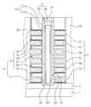
도 1은 본 발명의 실시예들에 따른 반도체소자를 설명하기 위한 평면도이다.
도 2는 본 발명의 일 실시예에 따른 반도체소자를 나타낸 수직 단면도이다.
도 3은 본 발명의 다른 실시예에 따른 반도체소자를 나타낸 수직 단면도이다.
도 4는 본 발명의 또 다른 실시예에 따른 반도체소자를 나타낸 수직 단면도이다.
도 5는 본 발명의 또 다른 실시예에 따른 반도체소자를 나타낸 수직 단면도이다.
도 6은 본 발명의 또 다른 실시예에 따른 반도체소자를 나타낸 수직 단면도이다.
도 7a는 본 발명의 또 다른 실시예에 따른 반도체소자를 나타낸 수직 단면도이다.
도 7b는 본 발명의 또 다른 실시예에 따른 반도체소자를 나타낸 수직 단면도이다.
도 7c는 본 발명의 또 다른 실시예에 따른 반도체소자를 나타낸 수직 단면도이다.
도 8은 본 발명의 또 다른 실시예에 따른 반도체소자를 나타낸 수직 단면도이다.
도 9는 본 발명의 또 다른 실시예에 따른 반도체소자를 설명하기 위한 평면도이다.
도 10a는 본 발명의 또 다른 실시예에 따른 반도체소자를 나타낸 수직 단면도이다.
도 10b는 본 발명의 또 다른 실시예에 따른 반도체소자를 나타낸 수직 단면도이다.
도 11은 본 발명의 실시예들에 따른 반도체소자의 제조방법을 설명하기 위한 평면도이다.
도 12a 내지 도 12k는 본 발명의 일 실시예에 따른 반도체소자의 제조방법을 설명하기 위한 수직 단면도들이다.
도 13a 및 도 13b는 본 발명의 다른 실시예에 따른 반도체소자의 제조방법을 설명하기 위한 수직 단면도들이다.
도 14a 및 도 14d는 본 발명의 또 다른 실시예에 따른 반도체소자의 제조방법을 설명하기 위한 수직 단면도들이다.
도 15a 내지 도 15c는 본 발명의 또 다른 실시예에 따른 반도체소자의 제조방법을 설명하기 위한 수직 단면도들이다.
도 16은 본 발명의 또 다른 실시예들에 따른 반도체소자의 제조방법을 설명하기 위한 평면도이다.
도 17a 내지 도 17e는 본 발명의 또 다른 실시예에 따른 반도체소자의 제조방법을 설명하기 위한 수직 단면도들이다.
도 18은 본 발명의 실시예에 따른 반도체 소자를 포함하는 전자 시스템을 도시한 블록도이다.
도 19는 본 발명의 실시예에 따른 반도체 소자를 구비한 메모리 카드를 도시한 블록도이다.
도 20은 본 발명 실시예에 따른 정보 처리 시스템을 도시한 블록도이다.1 is a plan view illustrating a semiconductor device according to example embodiments.
2 is a vertical cross-sectional view showing a semiconductor device according to an embodiment of the present invention.
3 is a vertical sectional view showing a semiconductor device according to another embodiment of the present invention.
4 is a vertical cross-sectional view of a semiconductor device according to still another embodiment of the present invention.
5 is a vertical cross-sectional view of a semiconductor device according to still another embodiment of the present invention.
6 is a vertical cross-sectional view of a semiconductor device according to still another embodiment of the present invention.
7A is a vertical cross-sectional view of a semiconductor device according to still another embodiment of the present invention.
7B is a vertical cross-sectional view of a semiconductor device according to still another embodiment of the present invention.
7C is a vertical cross-sectional view of a semiconductor device according to still another embodiment of the present invention.
8 is a vertical sectional view showing a semiconductor device according to another embodiment of the present invention.
9 is a plan view illustrating a semiconductor device according to still another embodiment of the present invention.
10A is a vertical cross-sectional view of a semiconductor device according to still another embodiment of the present invention.
10B is a vertical cross-sectional view of a semiconductor device according to still another embodiment of the present invention.
11 is a plan view illustrating a method of manufacturing a semiconductor device in accordance with embodiments of the present invention.
12A through 12K are vertical cross-sectional views illustrating a method of manufacturing a semiconductor device in accordance with an embodiment of the present invention.
13A and 13B are vertical cross-sectional views illustrating a method of manufacturing a semiconductor device in accordance with another embodiment of the present invention.
14A and 14D are vertical cross-sectional views illustrating a method of manufacturing a semiconductor device in accordance with still another embodiment of the present invention.
15A to 15C are vertical cross-sectional views illustrating a method of manufacturing a semiconductor device in accordance with still another embodiment of the present invention.
16 is a plan view illustrating a method of manufacturing a semiconductor device in accordance with still another embodiment of the present invention.
17A to 17E are vertical cross-sectional views illustrating a method of manufacturing a semiconductor device in accordance with still another embodiment of the present invention.
18 is a block diagram illustrating an electronic system including a semiconductor device according to an exemplary embodiment of the present invention.
19 is a block diagram illustrating a memory card including a semiconductor device according to an embodiment of the present invention.
20 is a block diagram illustrating an information processing system according to an embodiment of the present invention.
본 발명의 이점 및 특징, 그리고 그것들을 달성하는 방법은 첨부되는 도면과 함께 상세하게 후술되어 있는 실시예들을 참조하면 명확해질 것이다. 그러나 본 발명은 이하에서 개시되는 실시예들에 한정되는 것이 아니라 서로 다른 다양한 형태로 구현될 것이며, 단지 본 실시예들은 본 발명의 개시가 완전하도록 하며, 본 발명이 속하는 기술분야에서 통상의 지식을 가진 자에게 발명의 범주를 완전하게 알려주기 위해 제공되는 것이며, 본 발명은 청구항의 범주에 의해 정의될 뿐이다. 도면에서 층 및 영역들의 크기 및 상대적인 크기는 설명의 명료성을 위해 과장된 것일 수 있다. 명세서 전체에 걸쳐 동일 참조 부호는 동일 구성 요소를 지칭한다.Advantages and features of the present invention and methods for achieving them will be apparent with reference to the embodiments described below in detail with the accompanying drawings. However, the present invention is not limited to the embodiments disclosed below, but will be implemented in various forms, and only the present embodiments are intended to complete the disclosure of the present invention, and the general knowledge in the art to which the present invention pertains. It is provided to fully convey the scope of the invention to those skilled in the art, and the present invention is defined only by the scope of the claims. In the drawings, the sizes and relative sizes of layers and regions may be exaggerated for clarity. Like reference numerals refer to like elements throughout.
본 명세서에서 기술하는 실시예들은 본 발명의 이상적인 개략도인 단면도를 참고하여 설명될 것이다. 따라서, 제조 기술 및/또는 허용 오차 등에 의해 예시도의 형태가 변형될 수 있다. 따라서, 본 발명의 실시예들은 도시된 특정 형태로 제한되는 것이 아니라 제조 공정에 따라 생성되는 형태의 변화도 포함하는 것이다. 따라서, 도면에서 예시된 영역들은 개략적인 속성을 가지며, 도면에서 예시된 영역들의 모양은 소자의 영역의 특정 형태를 예시하기 위한 것이고, 발명의 범주를 제한하기 위한 것은 아니다.Embodiments described herein will be described with reference to cross-sectional views, which are ideal schematic diagrams of the invention. Accordingly, shapes of the exemplary views may be modified by manufacturing techniques and / or tolerances. Accordingly, the embodiments of the present invention are not limited to the specific forms shown, but also include variations in forms generated by the manufacturing process. Thus, the regions illustrated in the figures have schematic attributes, and the shape of the regions illustrated in the figures is intended to illustrate a particular form of region of the device, and is not intended to limit the scope of the invention.
도 1은 본 발명의 실시예들에 따른 반도체소자를 설명하기 위한 평면도이고, 도 2 내지 도 8은 도 1의 I-I'선을 따라 취해진 영역을 나타낸 수직 단면도들이다. 여기서, 도 2는 본 발명의 일 실시예에 따른 반도체소자를 나타낸 수직 단면도이고, 도 3은 본 발명의 다른 실시예에 따른 반도체소자를 나타낸 수직 단면도이고, 도 4는 본 발명의 또 다른 실시예에 따른 반도체소자를 나타낸 수직 단면도이고, 도 5는 본 발명의 또 다른 실시예에 따른 반도체소자를 나타낸 수직 단면도이고, 도 6은 본 발명의 또 다른 실시예에 따른 반도체소자를 나타낸 수직 단면도이고, 도 7a은 본 발명의 또 다른 실시예에 따른 반도체소자를 나타낸 수직 단면도이고, 도 7b는 본 발명의 또 다른 실시예에 따른 반도체소자를 나타낸 수직 단면도이고, 도 7c는 본 발명의 또 다른 실시예에 따른 반도체소자를 나타낸 수직 단면도이고, 도 8은 본 발명의 또 다른 실시예에 따른 반도체소자를 나타낸 수직 단면도이다.1 is a plan view illustrating a semiconductor device according to example embodiments of the inventive concept, and FIGS. 2 to 8 are vertical cross-sectional views illustrating regions taken along line II ′ of FIG. 1. 2 is a vertical sectional view showing a semiconductor device according to an embodiment of the present invention, Figure 3 is a vertical sectional view showing a semiconductor device according to another embodiment of the present invention, Figure 4 is another embodiment of the present invention 5 is a vertical cross-sectional view showing a semiconductor device according to another embodiment of the present invention, FIG. 6 is a vertical cross-sectional view showing a semiconductor device according to another embodiment of the present invention. 7A is a vertical sectional view showing a semiconductor device according to another embodiment of the present invention, FIG. 7B is a vertical sectional view showing a semiconductor device according to another embodiment of the present invention, and FIG. 7C is another embodiment of the present invention. 8 is a vertical cross-sectional view showing a semiconductor device according to the present invention, and FIG. 8 is a vertical cross-sectional view showing a semiconductor device according to another embodiment of the present invention.
우선, 도 1 및 도 2를 참조하여 본 발명의 일 실시예에 따른 반도체 소자에 대하여 설명하기로 한다.First, a semiconductor device according to an exemplary embodiment of the present invention will be described with reference to FIGS. 1 and 2.
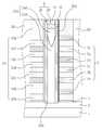
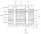
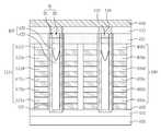
도 1 및 도 2를 참조하면, 기판(1)이 제공될 수 있다. 상기 기판(1)은 반도체 기판일 수 있다. 상기 기판(1)은 메모리 셀들이 형성되는 메모리 셀 영역(또는 셀 어레이 영역) 및 상기 메모리 셀들을 동작시키기 위한 주변 회로들이 형성되는 주변 회로 영역을 포함할 수 있다. 상기 기판(1)은 단결정 구조의 반도체 웨이퍼, 예를 들어 P형 실리콘 웨이퍼일 수 있다. 한편, 상기 기판(1)은 SOI층(silicon on insulating layer) 같은 반도체 박막(semiconductor film)을 포함할 수 있다.1 and 2, a
상기 기판(1) 내에 불순물 영역(3)이 제공될 수 있다. 상기 불순물 영역(3)은 포켓 웰 구조(pocket well structure) 또는 다중 웰 구조(multiple well structure) 일 수 있다. 상기 불순물 영역(3)은 p-형 웰을 포함할 수 있다.An
몇몇 실시예들에서, 상기 불순물 영역(3)은 표면 영역에 N+형, 즉 트랜지스터의 소오스 영역으로 정의되는 고농도의 N 형 영역을 포함할 수 있다. 예를 들어, 상기 불순물 영역(3)은 p-형의 웰 영역 및 상기 웰 영역의 일부 영역에 형성된 고농도의 N형 소오스 영역을 포함할 수 있다.In some embodiments, the
상기 기판(1) 상에 수평 패턴들(12)이 제공될 수 있다. 상기 수평 패턴들(12)의 각각은 상기 기판(1)의 주 표면에 대하여 수평일 수 있다. 상기 수평 패턴들(12)은 도전성 패턴들(6a, 6b, 6c, 6d, 6e, 6f) 및 층간 절연 패턴들(9a, 9b, 9c, 9d, 9e, 9f)을 포함할 수 있다. 상기 도전성 패턴들(6a, 6b, 6c, 6d, 6e, 6f)은 도전성 구조체(6)로 정의하고, 상기 층간 절연 패턴들(9a, 9b, 9c, 9d, 9e, 9f)은 층간 절연 구조체(9)로 정의할 수 있다.
상기 도전성 패턴들(6a, 6b, 6c, 6d, 6e, 6f)은 상기 층간 절연 패턴들(9a, 9b, 9c, 9d, 9e, 9f)에 의해 서로 이격되면서 적층될 수 있다. 그리고, 상기 도전성 패턴들(6a, 6b, 6c, 6d, 6e, 6f)은 상기 층간 절연 패턴들(9a, 9b, 9c, 9d, 9e, 9f)사이에 개재될 수 있다. 상기 층간 절연 패턴들(9a, 9b, 9c, 9d, 9e, 9f)은 실리콘 산화물, 실리콘 산질화물 또는 실리콘 질화물 등과 같은 절연성 물질로 형성될 수 있다. 상기 도전성 패턴들(6a, 6b, 6c, 6d, 6e, 6f)은 폴리 실리콘 또는 텅스텐 등을 포함하는 금속과 같은 도전성 물질로 형성될 수 있다.The
상기 수평 패턴들(12) 중 최상층에 위치하는 패턴은 층간 절연 패턴(9f)일 수 있다. 그리고, 상기 도전성 패턴들(6a, 6b, 6c, 6d, 6e, 6f) 중에서, 최하부에 위치하는 도전성 패턴(6a)은 상기 기판(1)과 이격될 수 있다.The pattern positioned on the uppermost layer of the
상기 수평 패턴들(12)을 관통하며 상기 기판(1)의 소정영역을 노출시키는 하나 또는 복수의 개구부(15)가 제공될 수 있다. 상기 개구부(15)는 홀 형상일 수 있다. 상기 수평 패턴들(15)의 각각은, 평면에서, 원 또는 다각형 형상의 상기 개구부(15)를 정의하는 플레이트 모양일 수 있다. 한편, 상기 수평 패턴들(15)의 각각은, 평면도에서, 가운데 부분에 상기 개구부(15)가 형성된 라인 형상일 수 있다.One or a plurality of
상기 개구부(15)의 상부 영역 내에 패드 패턴(18)이 제공될 수 있다. 상기 패드 패턴(18)의 상기 개구부(15) 내의 상기 수평 패턴들(12)의 측벽에 의해 둘러싸일 수 있다. 상기 패드 패턴(18)은 결정질 실리콘을 포함할 수 있다. 예를 들어, 상기 패드 패턴(18)은 폴리 실리콘막으로 형성될 수 있다.The
상기 패드 패턴(18) 하부에 제공되며 제1 갭필 패턴(21) 및 제2 갭필 패턴(24)을 포함하는 절연성의 갭필 구조체(27)가 제공될 수 있다. 상기 제1 및 제2 갭필 패턴들(21, 24)은 서로 다른 식각 선택비를 갖는 산화물들로 형성될 수 있다. 상기 제2 갭필 패턴(24)은, 산화물 에쳔트에 대하여, 상기 제1 갭필 패턴(21)보다 식각속도가 빠른 산화물로 형성될 수 있다. 여기서, 산화물 에쳔트는 불산(HF)을 포함하는 식각 용액일 수 있다.An insulating
상기 제1 갭필 패턴(21)은 제1 산화물을 포함할 수 있고, 상기 제2 갭필 패턴(24)은 상기 제1 산화물을 형성하기 위한 방법과 다른 방법으로 형성된 제2 산화물을 포함할 수 있다. 예를 들어, 상기 제1 갭필 패턴(21)은 ALD(atomic layer deposition) 방법과 같은 증착 방법에 의해 형성된 제1 산화물이고, 상기 제2 갭필 패턴(24)은 유동성 산화물(flowable oxide)을 이용하여 형성된 제2 산화물일 수 있다. 여기서, 상기 유동성 산화물은 F-CVD(flowable CVD) 방법에 의한 F-CVD 산화물(FCVD Oxide) 또는 스핀 코팅 방법에 의한 TOSZ(Tonen SilaZene) 일 수 있다. ALD 등과 같은 증착 방법에 의한 제1 산화물로 이루어진 제1 갭필 패턴(21)과 유동성 산화물을 이용하여 형성된 제2 산화물로 이루어진 제2 갭필 패턴(24)을 포함하는 상기 갭필 구조체(27)는 내부에 보이드(void) 등과 같은 결함이 없을 수 있다.The first
상기 제1 갭필 패턴(21)과 상기 제2 갭필 패턴(24)은 실리콘(Si) 및 산소(O)를 공통적으로 포함하면서, 서로 다른 원소를 포함할 수 있다. 예를 들어, 상기 제1 갭필 패턴(21)은 수소(H) 및 염소(Cl) 중 적어도 하나를 포함하고, 상기 제2 갭필 패턴(24)은 질소(N), 수소(H) 및 탄소(C) 중 적어도 하나를 포함할 수 있다.The first
상기 제1 및 제2 갭필 패턴들(21, 24)은 불순물을 함유한 실리콘 산화물로 형성되되, 상기 제1 갭필 패턴(21)은 수소 원소 및 염소 원소를 함유하는 실리콘 산화물(Si-H-Cl-O)로 형성될 수 있고, 상기 제2 갭필 패턴(24)은 질소 원소, 수소 원소 및 탄소 원소 중 적어도 하나를 포함하는 실리콘 산화물(Si-N-H-C-O 또는 Si-N-H-O)로 형성될 수 있다. 상기 제2 갭필 패턴(24)은 상기 제1 갭필 패턴(21)보다 낮은 밀도를 가질 수 있다.The first and second
상기 제1 갭필 패턴(21)은 상부면의 가운데 부분이 오목하게 함몰된 모양이고, 상기 제2 갭필 패턴(24)은 상기 제1 갭필 패턴(21)과 상기 패드 패턴(24) 사이에 개재될 수 있다.The first
상기 갭필 구조체(27)와 상기 개구부(15)의 측벽 사이에 개재됨과 아울러, 상기 패드 패턴(24)의 측벽과 상기 개구부(15)의 측벽 사이에 개재된 반도체 패턴(30)이 제공될 수 있다. 즉, 상기 반도체 패턴(30)은 상기 갭필 구조체(27)의 측벽 및 상기 패드 패턴(24)의 측벽을 둘러싸도록 제공될 수 있다.A
상기 반도체 패턴(30)으로부터 연장되어 상기 갭필 구조체(27)와 상기 기판(1) 사이에 개재된 반도체 패턴의 바닥부(30')가 제공될 수 있다. 즉, 상기 반도체 패턴(30)과 상기 반도체 패턴의 바닥부(30')는 연속적으로 연결된 하나의 막으로 형성될 수 있다. 상기 반도체 패턴(30)은 결정질 실리콘으로 이루어질 수 있다. 예를 들어, 상기 반도체 패턴(30)은 싱글 또는 폴리 실리콘으로 이루어질 수 있다.A
상기 기판(1)과 상기 반도체 패턴(30)은 다른 결정질의 실리콘으로 이루어질 수 있다. 예를 들어, 상기 기판(1)은 단결정 실리콘으로 이루어지고, 상기 반도체 패턴(30)은 폴리 실리콘으로 이루어질 수 있다.The
상기 패드 패턴(18)과 인접하는 상기 반도체 패턴 내에 제1 불순물 영역(D1)이 제공되고, 상기 패드 패턴(18) 내에 제2 불순물 영역(D2)이 제공될 수 있다. 상기 제1 및 제2 불순물 영역들(D1, D2)은 고농도의 N+ 불순물 영역(D)을 구성할 수 있다. 여기서, 상기 N+ 불순물 영역(D)은 드레인 영역으로 정의할 수 있다.A first impurity region D1 may be provided in the semiconductor pattern adjacent to the
한편, 상기 패드 패턴(18)과 상기 반도체 패턴(30)은 안정적인 콘택을 형성할 수 있다. 이에 대한 자세한 설명은 이후 도 12e 및 도 12f에서 설명 하기로 한다.Meanwhile, the
상기 반도체 패턴(30)과 상기 도전성 패턴들(6) 사이에 개재된 게이트 절연막(33)이 제공될 수 있다. 상기 게이트 절연막(33)은 터널 절연막(33t), 정보 저장 막(33s) 및 블로킹 절연막(33b)을 포함할 수 있다. 상기 터널 절연막(33t)은 상기 반도체 패턴(30)과 인접하고, 상기 블로킹 절연막(33b)은 상기 도전성 패턴들(6)에 인접하고, 상기 정보 저장 막(33s)은 상기 터널 절연막(30t)과 상기 블로킹 절연막(30b) 사이에 개재될 수 있다.A
상기 터널 절연막(30t)은 실리콘 산화막, 실리콘 산화 질화막(SiON layer), 질소 도핑된 실리콘 산화막(nitrogen doped Si Oxide layer) 및 고유전막 그룹(high-k dielectric group)으로 하나를 포함할 수 있다. 상기 고유전막 그룹은 알루미늄 산화막 (AlO layer), 지르코늄 산화막(ZrO layer), 하프늄 산화막(HfO layer) 및 란타늄 산화막(LaO layer) 등과 같이 실리콘 산화막보다 높은 유전 상수를 갖는 유전막을 포함할 수 있다.The tunnel insulating layer 30t may include one of a silicon oxide layer, a silicon oxynitride layer, a nitrogen doped silicon oxide layer, and a high-k dielectric group. The high dielectric layer group may include a dielectric layer having a higher dielectric constant than a silicon oxide layer, such as an aluminum oxide layer (AlO layer), a zirconium oxide layer (ZrO layer), a hafnium oxide layer (HfO layer), and a lanthanum oxide layer (LaO layer).
상기 정보 저장막(33s)은 플래시 메모리 소자 등과 같은 비휘발성 메모리 소자에서 정보를 저장하기 위한 막일 수 있다. 예를 들어, 상기 정보 저장막(33s)은 전하를 저장할 수 있는 트랩들을 갖는 막일 수 있다. 상기 정보 저장막(33s)은, 소자의 동작 조건에 따라, 상기 반도체 패턴(30)으로부터 상기 터널 절연막(30t)을 통하여 주입된 전자를 트랩하여 보유(retention) 하거나, 트랩된 전자를 소거할 수 있는 물질로 이루어질 수 있다. 예를 들어, 상기 정보 저장 막(33s)은 실리콘 산화 질화막(SiON), 실리콘 질화막 및 고유전막 그룹으로 구성된 일군에서 선택된 적어도 하나를 포함할 수 있다. 상기 블로킹 절연막(33b)은 실리콘 산화막 및 고유전막 그룹에서 적어도 하나를 포함할 수 있다.The
상기 게이트 절연막(33)은 상기 반도체 패턴(30)과 상기 도전성 패턴들(6) 사이에 개재되면서, 상기 도전성 패턴들(6)과 상기 절연 패턴들(9) 사이로 연장될 수 있다. 또한, 상기 게이트 절연막(33)은 상기 도전성 패턴들(6) 중 최하부의 도전성 패턴(6a)과 상기 기판(1) 사이에 개재될 수 있다.The
몇몇 실시예들에서, 상기 도전성 패턴들(6)의 측벽들과 상기 절연 패턴들(9)의 측벽들은 수직 정렬되지 않을 수 있다. In some embodiments, the sidewalls of the
상기 수평 패턴들(12)은 게이트 분리 절연막(36)에 의해 한정될 수 있다. 즉, 게이트 분리 절연막(36)은 상기 수평 패턴들(36)의 외측벽들을 둘러싸도록 형성될 수 있다. 상기 게이트 분리 절연막(36)은 실리콘 산화물 등과 같은 절연성 물질로 형성될 수 있다.The
상기 도전성 패턴들(6) 중에서, 최하부에 위치하는 도전성 패턴(6a)은 하부 선택 라인(LSL)으로 사용되고, 최상부에 위치하는 도전성 패턴(6f)은 상부 선택 라인(USL)으로 사용되고, 상기 하부 및 상부 선택 라인들(LSL, USL) 사이에 위치하는 도전성 패턴들(6b, 6c, 6d, 6e)은 비휘발성 메모리 소자의 워드라인들로 사용될 수 있다. 상기 하부 선택 라인(LSL)은 접지 선택 라인일 수 있고, 상기 상부 선택 라인은 스트링 선택 라인일 수 있다.
Of the
다른 실시예에서, 도 2에서 설명한 상기 반도체 패턴(30, 30')은 도 3에 도시된 바와 같은 반도체 패턴(30a)으로 변형될 수 있다. 좀더 구체적으로, 도 3에 도시된 바와 같이, 변형된 반도체 패턴(30a)은 상기 갭필 구조체(27)의 측벽 및 상기 패드 패턴(18)의 측벽을 둘러싸도록 형성되지만, 상기 갭필 구조체(27)와 상기 기판(1) 사이에 개재되지 않을 수 있다. 즉, 상기 기판(1) 또는 상기 불순물 영역(3)의 표면 또는 내부의 일부가 노출될 수 있고, 상기 갭필 구조체(27)와 직접적으로 접촉할 수 있다.
In another embodiment, the
또 다른 실시예에서, 도 2 에서 설명한 상기 갭필 구조체(27)는 도 4에 도시된 것과 같은 갭필 구조체(27a)로 변형될 수 있다. 좀더 구체적으로, 도 4에 도시된 것과 같이 변형된 갭필 구조체(27a)는 상기 패드 패턴(18)과 상기 기판(1) 사이에 형성된 기둥 형상의 제2 갭필 패턴(24a) 및 상기 제2 갭필 패턴(24a)의 측벽을 둘러싸는 제1 갭필 패턴(21a)을 포함할 수 있다.
In another embodiment, the
또 다른 실시예에서, 도 2에서 설명한 상기 반도체 패턴(30, 30') 및 상기 갭필 구조체(27)는 도 5에 도시된 것과 같은 반도체 패턴(30b) 및 갭필 구조체(27b)로 변형될 수 있다. 좀더 구체적으로, 도 5에 도시된 바와 같이 변형된 갭필 구조체(27b)는 상기 패드 패턴(18)과 상기 기판(1) 사이에 형성된 기둥 형상의 제2 갭필 패턴(24b) 및 상기 제2 갭필 패턴(24b)의 측벽을 둘러싸는 제1 갭필 패턴(21b)을 포함하고, 변형된 반도체 패턴(30b)은 상기 변형된 갭필 구조체(27b)의 측벽 및 상기 패드 패턴(18)의 측벽을 둘러싸도록 형성되지만, 상기 갭필 구조체(27b)와 상기 기판(1) 사이에 개재되지 않을 수 있다. 즉, 상기 기판(1) 또는 상기 불순물 영역(3)의 표면 또는 내부의 일부가 노출될 수 있고, 상기 갭필 구조체(27b)와 직접적으로 접촉할 수 있다.
In another embodiment, the
또 다른 실시예에서, 도 2에서 설명한 상기 갭필 구조체(27)는 도 6에 도시된 바와 같은 갭필 구조체(27c)로 변형될 수 있다. 좀더 구체적으로, 도 6에 도시된 바와 같이, 변형된 갭필 구조체(27c)는 상부면의 가운데 부분이 상기 개구부(15)의 중간 또는 그 이하의 하부 영역까지 오목하게 함몰된 제1 갭필 패턴(21c) 및 상기 제1 갭필 패턴(21c)과 상기 패드 패턴(18) 사이에 개재된 제2 갭필 패턴(24c)을 포함할 수 있다. 즉, 상기 제1 갭필 패턴(21c)의 일부는 상기 도전성 패턴들(6) 중 최상층에 위치한 도전성 패턴(67f)과 수평적으로 중첩될 수 있다. 그리고, 상기 제1 갭필 패턴(21c)의 상부면의 가운데 부분은 상기 개구부(15)의 하부 영역까지 함몰될 수 있다.
In another embodiment, the
다음으로, 도 7a를 참조하여 본 발명의 또 다른 실시예에 따른 반도체소자를 설명하기로 한다.Next, a semiconductor device according to still another embodiment of the present invention will be described with reference to FIG. 7A.
도 7a를 참조하면, 도 2에서와 마찬가지로, 기판(1) 내에 불순물 영역(3)이 제공될 수 있다. 상기 기판(1) 상에 수평 패턴들(12')이 제공될 수 있다. 상기 수평 패턴들(12')과 상기 기판(1) 사이에 버퍼 절연막(4)이 제공될 수 있다. 상기 버퍼 절연막(4)은 실리콘 산화물, 실리콘 질화물 또는 실리콘산질화물 등과 같은 절연성 물질로 형성될 수 있다.Referring to FIG. 7A, as in FIG. 2, an
상기 수평 패턴들(12')은 도전성 패턴들(6a', 6b', 6c', 6d', 6e', 6f') 및 층간 절연 패턴들(9a', 9b', 9c', 9d', 9e', 9f')을 포함할 수 있다. 상기 도전성 패턴들(6a', 6b', 6c', 6d', 6e', 6f')은 도전성 구조체(6')로 정의하고, 상기 층간 절연 패턴들(9a', 9b', 9c', 9d', 9e', 9f')은 층간 절연 구조체(9')로 정의할 수 있다. 상기 도전성 패턴들(6a', 6b', 6c', 6d', 6e', 6f')은 상기 층간 절연 패턴들(9a', 9b', 9c', 9d', 9e', 9f')에 의해 서로 이격되면서 적층될 수 있다.The horizontal patterns 12 'include
몇몇 실시예들에서, 상기 도전성 패턴들(6a', 6b', 6c', 6d', 6e', 6f')과 상기 층간 절연 패턴들(9a', 9b', 9c', 9d', 9e', 9f')의 측벽들은 수직 정렬될 수 있다. 도 2에서 설명한 것과 같이 상기 수평 패턴들(12')을 관통하며 상기 기판(1)의 소정영역을 노출시키는 하나 또는 복수의 개구부(15')가 제공될 수 있다.In some embodiments, the
상기 개구부(15')의 상부 영역 내에 패드 패턴(18)이 제공될 수 있다. 상기 패드 패턴(18)은 폴리 실리콘을 포함할 수 있다.The
도 2에서와 마찬가지로, 상기 패드 패턴(18)과 상기 기판(1) 사이에 형성되며 제1 갭필 패턴(21d) 및 제2 갭필 패턴(24d)을 포함하는 절연성의 갭필 구조체(27d)가 제공될 수 있다.As in FIG. 2, an insulating
다른 실시예들에서, 상기 갭필 구조체(27d)는 도 4 및 도 6에서와 같은 변형된 갭필 구조체(27a, 27b)로 변형될 수도 있다.In other embodiments, the
상기 갭필 구조체(27d) 및 상기 패드 패턴(18)의 측벽을 둘러싸는 반도체 패턴(30d)이 제공될 수 있다.A
한편, 상기 반도체 패턴(30d)은, 도 2에서의 상기 반도체 패턴(30)과 같이, 상기 반도체 패턴(30d)으로부터 연장되어 상기 갭필 구조체(27d)와 상기 기판(1) 사이에 개재된 반도체 패턴의 바닥부를 포함하도록 변형될 수 있다. 즉, 상기 기판(1) 또는 상기 불순물 영역(3) 상에 직접적으로 연장될 수 있다.Meanwhile, like the
상기 반도체 패턴(30d)과 상기 수평 패턴들(12') 사이에 개재된 게이트 절연막(33d)이 제공될 수 있다. 상기 게이트 절연막(33d)은 도 2에서와 마찬가지로 터널 절연막, 정보 저장 막 및 블로킹 절연막을 포함할 수 있다. 여기서, 상기 터널 절연막은 상기 반도체 패턴(30d)과 인접하고, 상기 블로킹 절연막은 상기 수평 패턴들(12')에 인접하고, 상기 정보 저장 막은 상기 터널 절연막과 상기 블로킹 절연막 사이에 개재될 수 있다.A
상기 수평 패턴들(12')은 게이트 분리 절연막(36')에 의해 한정될 수 있다. 즉, 게이트 분리 절연막(36')은 상기 수평 패턴들(36')의 외측벽들을 둘러싸도록 형성될 수 있다.The
다음으로, 도 7b를 참조하여 본 발명의 또 다른 실시예에 따른 반도체 소자를 설명하기로 한다.Next, a semiconductor device according to still another embodiment of the present invention will be described with reference to FIG. 7B.
도 7b를 참조하면, 도 2에서와 같이 불순물 영역(3)을 갖는 기판(1)이 제공될 수 있다. 상기 기판(1) 상에 수평 패턴들(7, 10)이 제공될 수 있다. 상기 수평 패턴들(7, 10)은 도전성 패턴들(7a, 7b, 7c, 7d, 7e, 7f) 및 층간 절연 패턴들(10a, 10b, 10c, 10d, 10e, 10f, 10g)을 포함할 수 있다. 상기 도전성 패턴들(7a, 7b, 7c, 7d, 7e, 7f)은 도전성 구조체(7)로 정의하고, 상기 층간 절연 패턴들(10a, 10b, 10c, 10d, 10e, 10f, 10g)은 층간 절연 구조체(10)로 정의할 수 있다. 상기 도전성 패턴들(7a, 7b, 7c, 7d, 7e, 7f)은 상기 층간 절연 패턴들(10a, 10b, 10c, 10d, 10e, 10f, 10g)에 의해 서로 이격되면서 적층될 수 있다. 상기 층간 절연 패턴들(10a, 10b, 10c, 10d, 10e, 10f, 10g) 중 최하부의 절연 패턴(10a)은 상기 도전성 패턴들(7a, 7b, 7c, 7d, 7e, 7f) 중 최하부의 도전성 패턴(7a) 하부에 위치할 수 있다. 상기 수평 패턴들(7, 10)의 측벽들에 의해 한정되는 개구부(16)가 제공될 수 있다. 상기 개구부(16)를 한정하는 상기 수평 패턴들(7, 10)의 측벽들은 수직정렬될 수 있다.Referring to FIG. 7B, a
상기 개구부(16) 내에 도 7a에서와 같은 반도체 패턴(30d), 게이트 절연막(33d), 갭필 구조체(27d), 패드 패턴(18)이 제공될 수 있다. 여기서, 상기 갭필 구조체(27d)는 도 5 및 도 6에서와 같은 갭필 구조체(27b, 27c)로 변형될 수 있다. 또한, 상기 반도체 패턴(30d)은 도 2에서와 같이 바닥부(30')를 갖는 반도체 패턴(30)으로 변형될 수 있다.The
다음으로, 도 7c를 참조하여 본 발명의 또 다른 실시예에 따른 반도체 소자를 설명하기로 한다.Next, a semiconductor device according to still another embodiment of the present invention will be described with reference to FIG. 7C.
도 7c를 참조하면, 도 2에서와 같이 불순물 영역(3)을 갖는 기판(1)이 제공될 수 있다. 상기 기판(1) 상에 수평 패턴들(7', 10')이 제공될 수 있다. 상기 수평 패턴들(7', 10')은 도전성 패턴들(7a', 7b', 7c', 7d', 7e', 7f') 및 층간 절연 패턴들(10a', 10b', 10c', 10d', 10e', 10f', 10g')을 포함할 수 있다. 상기 도전성 패턴들(7a', 7b', 7c', 7d', 7e', 7f')은 도전성 구조체(7')로 정의하고, 상기 층간 절연 패턴들(10a', 10b', 10c', 10d', 10e', 10f', 10g')은 층간 절연 구조체(10')로 정의할 수 있다. 상기 수평 패턴들(7', 10')의 측벽들에 의해 한정되는 개구부(16a)가 제공될 수 있다. 여기서, 상기 개구부(16a)를 한정하는 상기 수평 패턴들(7', 10')의 측벽들은 수직정렬되지 않을 수 있다. 즉, 상기 개구부(16a)를 한정하는 상기 도전성 구조체(8')의 측벽과 상기 층간 절연 구조체(10')의 측벽은 수직 정렬하지 않을 수 있다. 상기 개구부(16a) 내에서, 수평적으로 서로 마주보는 상기 도전성 패턴들(7a', 7b', 7c', 7d', 7e', 7f')의 측벽들 사이의 거리는, 수평적으로 서로 마주보는 상기 층간 절연 패턴들(10a', 10b', 10c', 10d', 10e', 10f', 10g')의 측벽들 사이의 거리보다 클 수 있다. 상기 도전성 구조체(8')의 측벽은 상기 층간 절연 구조체(10')와 수직적으로 중첩하며, 상기 층간 절연 구조체(10')의 측벽은 상기 도전성 구조체(8')와 수직적으로 중첩하지 않을 수 있다. 따라서, 상기 수평 패턴들(7', 10')에서, 상기 도전성 구조체(7')의 측벽이 옆으로 리세스되어 언더컷 영역이 정의될 수 있다.Referring to FIG. 7C, a
도 7c에서와 같이, 상기 개구부(16a)를 한정하는 상기 수평 패턴들(7', 10')의 측벽들이 수직정렬되지 않기 때문에, 상기 수평 패턴들(7', 10')의 측벽들과 인접하는 상기 반도체 패턴(31)의 측벽은 수직하지 않을 수 있다. 상기 반도체 패턴(31)과 상기 수평 패턴들(7', 10') 사이에 게이트 절연막(34a)이 제공될 수 있다. 상기 게이트 절연막(34a)은 도 2에서와 마찬가지로 터널 절연막, 정보 저장 막 및 블로킹 절연막을 포함할 수 있다. 상기 게이트 절연막(34a)은 상기 도전성 구조체(7')의 언더컷 영역에 형성될 수 있다.As shown in FIG. 7C, the sidewalls of the
상기 반도체 패턴(31)은 상기 개구부(16a)의 측벽에만 형성될 수 있다. 그렇지만, 본 발명은 이에 한정되지 않는다. 예를 들어, 상기 반도체 패턴(31)은 도 2에서의 상기 반도체 패턴(30)과 같이, 상기 반도체 패턴(31)으로부터 연장되어 상기 갭필 구조체(28a)와 상기 기판(1) 사이에 개재된 반도체 패턴의 바닥부를 포함할 수 있다.The
상기 개구부(16a)의 상부 영역 내에 도 7a에서와 같은 패드 패턴(19)이 제공될 수 있다. 도 2에서와 마찬가지로, 상기 패드 패턴(19)과 상기 기판(1) 사이에 형성되며 제1 갭필 패턴(22a) 및 제2 갭필 패턴(25a)을 포함하는 절연성의 갭필 구조체(28a)가 제공될 수 있다.A
다른 실시예에서, 상기 갭필 구조체(28a)는 도 4 및 도 6에서와 같은 변형된 갭필 구조체(27a, 27b)로 변형될 수도 있다.In other embodiments, the
도 8을 참조하여 본 발명의 또 다른 실시예에 따른 반도체 소자를 설명하기로 한다. 도 8을 참조하면, 도 2에서 설명한 것과 같이, 기판(1) 내에 불순물 영역(3)이 제공될 수 있다. 도 7a에서 설명한 것과 같이 상기 기판(1) 상에 수평 패턴들(12')이 제공되고, 상기 수평 패턴들(12')과 상기 기판(1) 사이에 버퍼 절연막(4)이 제공될 수 있다A semiconductor device according to another embodiment of the present invention will be described with reference to FIG. 8. Referring to FIG. 8, as described with reference to FIG. 2, an
상기 수평 패턴들(12')은, 도 7a에서와 마찬가지로, 도전성 패턴들(6a'~ 6f') 및 층간 절연 패턴들(9a'~9f')을 포함할 수 있다. 상기 도전성 패턴들(6a'~6f')은 도전성 구조체(6')로 정의하고, 상기 층간 절연 패턴들(9a'~ 9f')은 층간 절연 구조체(9')로 정의할 수 있다.As in FIG. 7A, the
상기 수평 패턴들(12')의 외측벽들을 둘러싸는 게이트 분리 절연막(36)이 제공될 수 있다. 상기 게이트 분리 절연막(36)은 실리콘 산화물 등과 같은 절연성 물질로 형성될 수 있다.A gate
상기 수평 패턴들(12') 및 상기 게이트 분리 절연막(36)을 덮는 캡핑 절연 패턴(39)이 제공될 수 있다. 따라서, 상기 캡핑 절연 패턴(39)은 상기 수평 패턴들(12')보다 넓은 평면적 및 넓은 폭을 가질 수 있다. 상기 캡핑 절연 패턴(39)은 실리콘 산화물, 실리콘 질화물 또는 실리콘산질화물 등과 같은 절연성 물질로 이루어질 수 있다.A capping insulating
상기 캡핑 절연 패턴(39) 및 상기 수평 패턴들(12')을 관통하는 하나 또는 복수의 개구부(15')가 제공될 수 있다. 상기 개구부(15')의 상부 영역 내에 패드 패턴(18e)이 제공될 수 있다. 상기 패드 패턴(18e)은 폴리 실리콘을 포함할 수 있다. 도 2에서와 마찬가지로, 상기 패드 패턴(18e)과 상기 기판(1) 사이에 형성되며 제1 갭필 패턴(21e) 및 제2 갭필 패턴(24e)을 포함하는 절연성의 갭필 구조체(27e)가 제공될 수 있다. 다른 실시예들에서, 상기 갭필 구조체(27e)는 도 4 및 도 6에서와 같은 변형된 갭필 구조체(27a, 27b)로 변형될 수도 있다.One or a plurality of
상기 갭필 구조체(27e)의 측벽 및 상기 패드 패턴(18e)의 측벽을 둘러싸는 반도체 패턴(30e)이 제공될 수 있다. 상기 반도체 패턴(30e)으로부터 연장되어 상기 갭필 구조체(27e)와 상기 기판(1) 사이에 개재된 반도체 패턴의 바닥부(30e')가 제공될 수 있다. 즉, 상기 반도체 패턴(30e)과 상기 반도체 패턴의 바닥부(30')는 연속적으로 연결된 하나의 막으로 형성될 수 있다. 다른 실시예에서, 상기 바닥부(30')는 생략될 수 있다.A
상기 반도체 패턴(30e)과 상기 수평 패턴들(12') 사이에 개재된 게이트 절연막(33e)이 제공될 수 있다. 상기 게이트 절연막(33e)은 도 2에서와 같이 터널 절연막, 정보 저장 막 및 블로킹 절연막을 포함할 수 있다. 즉, 상기 기판(1) 또는 상기 불순물 영역(3)의 표면 또는 내부의 일부가 노출될 수 있고, 상기 갭필 구조체(27e)와 직접적으로 접촉할 수 있다.
A
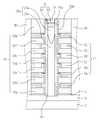
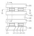
다음으로, 도 9, 도 10a 및 도 10b를 참조하여 본 발명의 또 다른 실시예들에 따른 반도체소자를 설명하기로 한다. 도 10a 및 도 10b에서, "E"로 표시된 부분은 도 9의 II-II'선을 따라 취해진 영역이고, "F"로 표시된 부분은 도 9의 III-III'선을 따라 취해진 영역이다.Next, a semiconductor device according to still other embodiments of the present invention will be described with reference to FIGS. 9, 10A, and 10B. In Figs. 10A and 10B, the portion indicated by "E" is a region taken along the line II-II 'of Fig. 9, and the portion denoted by "F" is the region taken along the line III-III' of Fig. 9.
도 9 및 도 10a을 참조하면, 도 2에서와 같이 반도체 물질로 이루어진 기판(50) 내에 불순물 영역(53)이 제공될 수 있다. 상기 기판(50) 상에 수평 패턴들(50)이 제공될 수 있다. 상기 수평 패턴들(50)은 도전성 패턴들(56a, 56b, 56c, 56d, 56e, 56f) 및 층간 절연 패턴들(59a, 59b, 59c, 59d, 59e, 59f)을 포함할 수 있다. 상기 도전성 패턴들(56a, 56b, 56c, 56d, 56e, 56f)은 도전성 구조체(56)로 정의하고, 상기 층간 절연 패턴들(59a, 59b, 59c, 59d, 59e, 59f)은 층간 절연 구조체(59)로 정의할 수 있다. 상기 도전성 패턴들(56a, 56b, 56c, 56d, 56e, 56f)은 상기 층간 절연 패턴들(59a, 59b, 59c, 59d, 59e, 59f)에 의해 서로 이격되면서 적층될 수 있다. 그리고, 상기 도전성 패턴들(56a, 56b, 56c, 56d, 56e, 56f)은 상기 층간 절연 패턴들(59a, 59b, 59c, 59d, 59e, 59f)사이에 개재될 수 있다.9 and 10A, an
상기 수평 패턴들(62)을 관통하며 상기 기판(50)의 소정영역을 노출시키는 하나 또는 복수의 개구부(65)가 제공될 수 있다. 상기 개구부(65)는 라인 형상일 수 있다. 따라서, 평면도로 보았을 때, 상기 수평 패턴들(62)은 서로 이격된 라인 형상일 수 있다. 상기 개구부(65)를 한정하는 상기 도전성 패턴들(56)과 상기 절연성 패턴들(59)의 측벽들은 수직 정렬되지 않을 수 있다.One or a plurality of
상기 개구부(65) 내에 서로 이격된 절연성 기둥들(89)이 제공될 수 있다. 상기 절연성 기둥들(89)은 실리콘 산화물, 실리콘 질화물 또는 실리콘산질화물 등과 같은 절연성 물질로 이루어질 수 있다.Insulating
상기 절연성 기둥들(89) 사이의 상기 개구부(65) 내에 갭필 구조체(77)가 제공될 수 있다. 상기 갭필 구조체(77)는 제1 갭필 패턴(71) 및 제2 갭필 패턴(77)을 포함할 수 있다. 상기 갭필 구조체(77)는, 수직 단면도로 보았을 때, 도 2에서의 갭필 구조체(27)와 동일한 형태일 수 있다. 따라서, 상기 갭필 구조체(77)는 도 2에서의 갭필 구조체(27)와 마찬가지로, 도 4에서와 같은 갭필 구조체(27a)도 6에서와 같은 갭필 구조체(27c)로 변형될 수 있다.A
상기 절연성 기둥들(89) 사이의 상기 갭필 구조체(77) 상부에 패드 패턴(68)이 제공될 수 있다. 즉, 상기 패드 패턴(68)은 상기 갭필 구조체(77) 상부에 형성되며 상기 절연성 기둥들(89) 사이에 위치할 수 있다. 상기 패드 패턴(68)은 폴리 실리콘으로 형성될 수 있다.A
상기 패드 패턴(68)의 측벽과 상기 수평 패턴들(62)의 측벽들 사이에 개재됨과 아울러, 상기 갭필 구조체(77)의 측벽과 상기 수평 패턴들(62)의 측벽들 사이에 개재된 반도체 패턴(80)이 제공될 수 있다. 상기 반도체 패턴(80)은 결정질 실리콘으로 이루어질 수 있다. 예를 들어, 상기 반도체 패턴(80)은 폴리 실리콘으로 이루어질 수 있다.A semiconductor pattern interposed between the sidewall of the
상기 반도체 패턴(80)으로부터 연장되어 상기 갭필 구조체(77)와 상기 기판(1) 사이에 개재된 반도체 패턴의 바닥부(80')가 제공될 수 있다. 다른 실시예에서, 상기 반도체 패턴의 바닥부(80')는 생략될 수 있다.A
상기 반도체 패턴(80)과 상기 도전성 패턴들(56) 사이에 게이트 절연막(83)이 제공될 수 있다. 상기 게이트 절연막(80)은 도 2에서와 같이 터널 절연막, 정보 저장 막 및 블로킹 절연막을 포함할 수 있다.A
상기 게이트 절연막(80)은 상기 반도체 패턴(80)과 상기 도전성 패턴들(56) 사이에 개재되면서, 상기 도전성 패턴들(56)과 상기 절연 패턴들(59) 사이로 연장될 수 있다. 또한, 상기 게이트 절연막(83)은 상기 도전성 패턴들(56) 중 최하부의 도전성 패턴(56a)과 상기 기판(50) 사이에 개재될 수 있다.The
상기 수평 패턴들(62)의 외측벽들을 둘러싸는 게이트 분리 절연막(89)이 제공될 수 있다. 상기 게이트 분리 절연막(89)은 실리콘 산화물 등과 같은 절연성 물질로 형성될 수 있다.
A gate
다른 실시예에서, 상기 개구부(65)을 한정하는 상기 도전성 패턴들(56) 및 상기 층간 절연 패턴들(59)은 도 10b에 도시된 바와 같이 변형될 수 있다. 좀더 구체적으로, 도 10b에 도시된 바와 같이, 상기 개구부(65)를 한정하는 변형된 도전성 패턴들(56') 및 변형된 층간 절연 패턴들(59')의 측벽들은 수직정렬될 수 있다. 또한, 상기 게이트 절연막(83)은 변형된 도전성 패턴들(56')과 변형된 층간 절연 패턴들(59') 사이로 연장되지 않고, 상기 개구부(65)를 한정하는 변형된 도전성 패턴들(56') 및 변형된 층간 절연 패턴들(59')의 측벽들과 상기 반도체 패턴(80) 사이에 개재되도록 변형될 수 있다.
In another embodiment, the
이하에서, 본 발명의 실시예들에 따른 반도체소자의 제조방법들을 설명하기로 한다.Hereinafter, methods of manufacturing semiconductor devices according to embodiments of the present invention will be described.
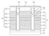
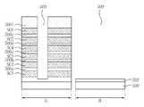
도 11은 본 발명의 실시예들에 따른 반도체소자의 제조방법을 설명하기 위한 평면도이고, 도 12a 내지 도 12k는 본 발명의 일 실시예에 따른 반도체소자의 제조방법을 설명하기 위한 수직 단면도들이다.11 is a plan view illustrating a method of manufacturing a semiconductor device in accordance with embodiments of the present invention, and FIGS. 12A to 12K are vertical cross-sectional views illustrating a method of manufacturing a semiconductor device in accordance with an embodiment of the present invention.
도 12a를 참조하면, 도 2에서와 같은 기판(100)이 제공될 수 있다. 상기 기판(100)은 반도체 기판일 수 있다. 상기 기판(100)은 메모리 셀들이 형성되는 메모리 셀 영역(또는 셀 어레이 영역) 및 상기 메모리 셀들을 동작시키기 위한 주변 회로들이 형성되는 주변 회로 영역을 포함할 수 있다. 상기 기판(100)은 단결정 구조의 반도체, 예를 들어 P형 실리콘 웨이퍼일 수 있다. 상기 기판(100) 내에 불순물 영역(103)이 형성될 수 있으며, 상기 불순물 영역(103)은 포켓 웰 구조(pocket well structure) 또는 다중 웰 구조(multiple well structure)로 형성될 수 있다.Referring to FIG. 12A, a
몇몇 실시예들에서, 상기 불순물 영역(103)은 표면 영역에 N+형, 즉 트랜지스터의 소오스 영역으로 정의되는 고농도의 N 형 영역을 포함할 수 있다. 예를 들어, 상기 불순물 영역(103)은 p-형의 웰 영역 및 상기 웰 영역의 일부 영역에 형성된 고농도의 N형 소오스 영역을 포함할 수 있다.In some embodiments, the
상기 기판(100) 상에 희생 막들(SC1, SC2, SC3, SC4, SC5, SC6) 및 층간 절연막들(106a, 106b, 106c, 106d, 106e, 106f)을 교대로 형성할 수 있다. 따라서, 희생막 구조체(SC)를 구성하는 상기 희생 막들(SC1~SC6)은 상기 층간 절연막들(106a~106f)에 의해 서로 이격되면서 적층될 수 있다. 그리고, 상기 희생 막들(SC1~SC6) 사이에 개재되는 상기 층간 절연막들(106a~106f)은 층간 절연 구조체(106)를 구성할 수 있다.Sacrificial layers SC1, SC2, SC3, SC4, SC5 and SC6 and interlayer insulating
상기 층간 절연막들(106a~106f)은 실리콘 산화물, 실리콘 산질화물 또는 실리콘 질화물 등과 같은 절연성 물질로 형성할 수 있다. 상기 희생 막들(SC1~SC6)은 상기 층간절연막들(106a~106f)의 식각을 최소화하면서 선택적으로 제거할 수 있는 물질로 형성할 수 있다.The
한편, 상기 층간절연막 보다 상기 희생 막을 먼저 형성할 수 있다. 예를 들어, 도시된 것처럼 상기 희생 막들(SC1~SC6) 중에서 가장 먼저 형성되는 희생막(SC1)은 상기 층간절연막들(106a~106f) 중에서 가정 먼저 형성되는 층간절연막(106a) 보다 상기 기판(100)에 인접하게 형성될 수 있다. 또한, 상기 희생 막들(SC1~SC6) 중에서 가장 마지막에 형성되는 희생막(SC6)은 상기 층간 절연막들(106a~106f) 중에서 가장 마지막에 형성되는 층간 절연막(106f)에 의해 덮이도록 형성될 수 있다.The sacrificial film may be formed before the interlayer insulating film. For example, as illustrated, the first sacrificial film SC1 formed of the sacrificial films SC1 to SC6 is formed on the
몇몇 실시예들에서, 가장 먼저 형성되는 상기 희생막(SC1)과 기판(100) 사이에 버퍼 막(미도시)이 형성될 수 있다. 예를 들어, 상기 버퍼 막은 실리콘 산화물로 형성할 수 있다.In some embodiments, a buffer layer (not shown) may be formed between the first sacrificial layer SC1 and the
도 11 및 도 12b를 참조하면, 상기 층간절연 구조체(106) 및 상기 희생막 구조체(SC)를 패터닝하여 상기 기판(100)의 상부면을 노출시키는 개구부들(109)을 형성할 수 있다. 즉, 상기 개구부들(109)은 상기 층간절연 구조체(106), 상기 희생막 구조체(SC)을 관통하며 상기 기판(100)의 상부면을 노출시킬 수 있다. 상기 개구부들(109)은 홀 형태로 형성될 수 있다.11 and 12B, the
도 11 및 도 12c를 참조하면, 상기 개구부들(109)을 갖는 기판을 콘포멀하게 덮는 예비 반도체 막을 형성할 수 있다. 따라서, 상기 예비 반도체 막은 상기 개구부들(109)의 측벽들 및 상기 개구부들(109)에 의해 노출된 상기 기판(100)을 덮도록 형성되며, 상기 개구부들(109)의 측벽들 사이의 가운데 부분을 채우지 않도록 형성될 수 있다. 즉, 각각의 상기 개구부들(109)의 폭은 상기 예비 반도체 막의 두께보다 2배 이상 클 수 있다.11 and 12C, a preliminary semiconductor film conformally covering a substrate having the
상기 예비 반도체 막은 화학기상 증착(CVD) 기술 또는 원자층 증착(ALD) 기술을 사용하여 실리콘 및 실리콘 저마늄 중 적어도 하나를 포함하는 물질로 형성할 수 있다. 예를 들어, 상기 예비 반도체 막은 비결정질 실리콘막으로 형성할 수 있다.The preliminary semiconductor film may be formed of a material including at least one of silicon and silicon germanium using chemical vapor deposition (CVD) or atomic layer deposition (ALD). For example, the preliminary semiconductor film may be formed of an amorphous silicon film.
상기 예비 반도체 막을 결정화시키기 위한 열처리 공정을 진행하여, 반도체 막(112)을 형성할 수 있다. 상기 열처리 공정은 약500℃ 내지 약1000℃의 온도로 수행될 수 있다.The heat treatment process for crystallizing the preliminary semiconductor film may be performed to form the
상기 예비 반도체 막은 열처리 공정에 의하여 결정질의 반도체 막(112)으로 형성될 수 있다. 예를 들어, 상기 반도체 막(112)은 다결정 구조의 반도체 물질로 형성될 수 있다. 상기 반도체 막(112)은 폴리 실리콘막으로 형성될 수 있다. The preliminary semiconductor film may be formed of the
상기 반도체 막(112)을 갖는 기판 상에 상기 개구부(109)를 채우는 절연성의 제1 예비 갭필 막을 형성하고, 상기 제1 예비 갭필 막을 부분 식각하여 제1 갭필 패턴(115)을 형성할 수 있다. 상기 제1 갭필 패턴(115)은 상부면의 가운데 부분이 오목하게 함몰된 모양으로 형성될 수 있다.An insulating first preliminary gap fill layer may be formed on the substrate having the
상기 제1 갭필 패턴(115)은 절연성 산화물로 형성할 수 있다. 예를 들어, 상기 제1 갭필 패턴(115)을 형성하는 것은 ALD(atomic layer deposition) 또는 CVD(chemical vapor deposition)와 같은 증착 방법을 이용하여 실리콘 산화물 등과 같은 절연성 산화물을 형성하고, 상기 개구부들(109)을 부분적으로 채우도록 상기 절연성 산화물을 부분 식각하는 것을 포함할 수 있다. 여기서, 상기 절연성 산화물을 부분식각 하는 것은 건식 식각(dry etch) 공정을 이용할 수 있다.The first
다른 실시예에서, 상기 제1 갭필 패턴(115)은 도 3에서 설명한 제1 갭필 패턴(21a)과 같은 형태로 변형될 수 있다. 보다 구체적으로, 상기 반도체 막(112)을 갖는 기판 상에 상기 개구부(109)를 완전히 채우지 않도록 상기 개구부(109)의 측벽 및 바닥면을 따라 일정한 두께로 제1 예비 갭필 막을 형성하고, 상기 제1 예비 갭필 막을 이방성 식각하여 상기 개구부(109)의 측벽에 잔존하는 제1 갭필 패턴을 형성할 수 있다.In another embodiment, the first
또 다른 실시예에서, 상기 제1 갭필 패턴(115)은 도 6에서 설명한 제1 갭필 패턴(21c)과 같은 형태로 변형될 수 있다. 보다 구체적으로, 상기 반도체 막(112)을 갖는 기판 상에 상기 개구부(109)를 채우되, 내부에 보이드(void) 또는 심(seam)이 형성된 제1 예비 갭필 막을 형성하고, 상기 제1 예비 갭필 막을 이방성 식각하여 도 6에서 설명한 제1 갭필 패턴(21c)과 같은 형태로 변형된 제1 갭필 패턴을 형성할 수 있다. 이 경우에, 상기 예비 갭필 막 내의 보이드 또는 심(seam) 등을 통하여 침투하는 식각 가스에 의하여 상기 예비 갭필 막은 보다 깊이 식각되어, 제1 갭필 패턴의 상부면의 가운데 부분이 상기 개구부(109)의 중간 또는 하부 영역까지 함몰될 수 있다. 이와는 달리, 상기 반도체 막(112)을 갖는 기판 상에 상기 개구부(109)의 하부 영역은 완전히 채우면서 상기 개구부(109)의 상부 영역은 완전히 채우지 않는 제1 예비 갭필 막을 형성하고, 상기 제1 예비 갭필 막을 이방성 식각하여 도 6에서 설명한 제1 갭필 패턴(21c)과 같은 형태로 변형된 제1 갭필 패턴을 형성할 수 있다.
In another embodiment, the first
도 11 및 도 12d를 참조하면, 상기 제1 갭필 패턴(115) 상에 제2 예비 갭필 막을 형성할 수 있다. 상기 제2 예비 갭필 막은 상기 제1 갭필 패턴(115)과 다른 방법으로 형성된 산화물일 수 잇다. 예를 들어, 상기 제1 갭필 패턴(115)은 ALD(atomic layer deposition) 또는 CVD(chemical vapor deposition)와 같은 증착 방법에 의한 산화물로 형성하고, 상기 제2 예비 갭필 막은 유동성 산화물(flowable oxide)로 형성할 수 있다. 여기서, 상기 유동성 산화물은 F-CVD(floawable CVD) 방법 또는 스핀 코팅 방법에 의한 산화물일 수 있다. 예를 들어, 상기 유동성 산화물은 F-CVD 산화물(FCVD Oxide) 또는 TOSZ(Tonen SilaZene)일 수 있다.11 and 12D, a second preliminary gap fill layer may be formed on the first
이어서, 상기 유동성 산화물로 형성된 상기 제2 예비 갭필 막을 경화시키기 위한 열처리 공정을 진행할 수 있다. 상기 경화된 제2 예비 갭필 막은 상기 제1 갭필 패턴(115)보다 낮은 밀도를 가질 수 있다. 상기 제2 예비 갭필 막을 경화시키기 위한 열처리 공정은 약500℃ 내지 약1000℃의 온도 범위에서 수행될 수 있다. 여기서, 상기 제2 예비 갭필 막을 경화시키기 위한 열처리 온도는, 상기 반도체 막(112)의 특성을 변화시키지 않게 하기 위하여, 상기 예비 반도체 막을 결정화시키기 위한 열처리 온도와 같거나 낮을 수 있다. 여기서, 상기 예비 갭필 막을 경화시키기 위한 열처리 공정 동안에, 상대적으로 밀도가 높은 상기 제1 갭필 패턴(115)의 부피 변화는 없거나 무시해도 좋을 정도로 미세할 수 있다.Subsequently, a heat treatment process may be performed to cure the second preliminary gapfill film formed of the flowable oxide. The cured second preliminary gap fill layer may have a lower density than the first
한편, 상기 예비 갭필 막이 경화되면서, 상기 예비 갭필 막은 수축(shrink)될 수 있다. 이 경우에, 상기 개구부(109)의 대부분을, 상대적으로 밀도가 높고 상기 예비 갭필 막을 경화시키기 위한 열처리 동안에 영향을 받지 않는 상기 제1 갭필 패턴(115)이 채우고 있기 때문에, 상기 예비 갭필 막의 수축으로 인한 소자의 열화를 방지할 수 있다.Meanwhile, as the preliminary gapfill film is cured, the preliminary gapfill film may shrink. In this case, since most of the
한편, 상기 제1 갭필 패턴(115)이 도 4 또는 도 6에서의 제1 갭필 패턴들(21a, 21c)과 같이 변형될지라도, 채널 영역으로 사용되는 상기 반도체 막(112)을 상기 제1 갭필 패턴(115)이 덮고 있기 때문에, 상기 예비 갭필 막의 수축으로 인한 소자의 특성, 특히 상기 반도체 막(112)의 열화를 방지할 수 있다.Meanwhile, even if the first
경화된 상기 제2 예비 갭필 막에 대하여, 상기 층간 절연막들(106a~106f) 상의 상기 반도체 막(112)이 노출될 때까지 평탄화하여 제2 갭필 막(118)을 형성할 수 있다. 따라서, 상기 제2 갭필 막(118)은 상기 제1 갭필 패턴(115)에 대하여 식각 선택비를 갖는 산화물로 형성될 수 있다. 즉, 상기 제2 갭필 막(118)은 상기 제1 갭필 패턴(115)보다, 산화물 에쳔트에 대하여 식각속도가 빠른 산화물로 형성될 수 있다. 예를 들어, 상기 제2 갭필 막(118)은 상기 제1 갭필 패턴(115)보다, 불산(HF)을 포함하는 습식 식각 용액에 대하여 식각속도가 약 10배 이상 빠른 산화물로 형성될 수 있다.The cured second preliminary gap fill layer may be planarized to form a second
상기 제1 갭필 패턴(115)과 상기 제2 갭필 막(118)은 실리콘(Si) 및 산소 원소(O)를 공통적으로 포함하면서, 서로 다른 원소를 포함할 수 있다. 예를 들어, 상기 제1 갭필 패턴(115)은 수소(H) 및 염소(Cl)를 포함하고, 상기 제2 갭필 막(118)은 질소(N), 수소(H) 및 탄소(C) 중 적어도 하나를 포함할 수 있다. 상기 제1 갭필 패턴(115)은 수소 원소 및 염소 원소를 함유하는 실리콘 산화물(Si-H-Cl-O)로 이루어지고, 상기 제2 갭필 막(118)은 질소 원소, 수소 원소 및 탄소 원소 중 적어도 하나를 포함하는 실리콘 산화물(Si-N-H-C-O 또는 Si-N-H-O)로 이루어질 수 있다.
The first
도 11 및 도 12e를 참조하면, 상기 제2 갭필 막(118)을 부분 식각하여 제2 갭필 패턴(119)을 형성할 수 있다. 상기 제1 및 제2 갭필 패턴들(115, 119)은 갭필 구조체(121)를 구성할 수 있다. 상기 제2 갭필 막(118)에 대하여 등방성 또는 이방성 식각 공정을 진행하여 상기 제2 갭필 막(118)을 부분 식각할 수 있다.11 and 12E, the second
상기 제2 갭필 패턴(119) 하부에는 ALD 기술에 의한 산화물로 이루어진 상기 제1 갭필 패턴(115)이 형성되고, 상기 제1 갭필 패턴(115) 상에 형성되는 상기 제2 갭필 패턴(119)은 열처리에 의해 경화되는 과정에서 수축 량이 최소화되기 때문에, 상기 갭필 구조체(121)의 내부에 보이드(void) 등과 같은 결함이 형성되는 것은 방지될 수 있다.The first
상기 제2 갭필 막(118)을 부분 식각하는 것은 상기 반도체 막(112)을 식각 손상시키지 않는 습식 식각 공정을 이용하여 수행될 수 있다. 예를 들어, 상기 제2 갭필 막(118)을 F-CVD 산화물 또는 TOSZ로 형성하는 경우에, 상기 제2 갭필 막(118)은 불산(HF)을 함유하는 식각 용액을 사용하여 식각할 수 있다. 그러나, 건식 이방성 식각 공정이 배제된다는 의미는 아니다.Partial etching of the
상기 제2 갭필 막(118)을 부분 식각함으로 인하여 상기 반도체 막(112)의 일부 표면이 노출될 수 있다. 상기 제2 갭필 막(118)은 상기 제1 갭필 패턴(115) 보다 쉽게 식각될 수 있는 산화물로 형성되기 때문에, 상기 제2 갭필 막(118)을 부분 식각함으로 인하여 노출되는 상기 반도체 막(112)의 표면에 산화물이 잔류하지 않는다.Partial etching of the
또한, 상기 제2 갭필 막(118)을 부분 식각함으로 인하여 노출되는 상기 반도체 막(112)의 표면에 산화물이 잔류하지 않기 때문에, 과도한 과 식각(over etch)을 하지 않는다. 즉, 상기 제2 갭필 막(118)의 식각량을 쉽게 제어할 수 있기 때문에, 산포 특성을 향상시킬 수 있다.
In addition, since no oxide remains on the surface of the
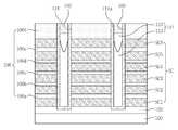
도 11 및 도 12f를 참조하면, 상기 제2 갭필 패턴(119)을 갖는 기판 상에 상기 개구부(109)의 나머지 부분을 채우며 상기 층간 절연막(106)을 덮는 패드 막을 형성하고, 상기 층간 절연막들(106a~106f) 중 최상부에 위치하는 층간 절연막(106f)이 노출될 때까지 평탄화할 수 있다. 그 결과, 상기 제2 갭필 패턴(119) 상에 상기 개구부(109)의 나머지 부분을 채우는 패드 패턴(124)이 형성될 수 있다. 또한, 상기 반도체 막(112)은 상기 개구부(109) 내에 잔존하여 반도체 패턴(112a)으로 형성될 수 있다. 즉, 상기 반도체 패턴(112a)은 상기 갭필 구조체(121)의 측벽 및 상기 패드 패턴(124)의 측벽을 둘러싸면서 상기 갭필 구조체(121)의 바닥면을 덮도록 형성될 수 있다. 상기 평탄화는 화학기계적 연마 기술(CMP) 및/또는 에치백 기술을 이용하여 수행할 수 있다. 상기 패드 패턴(124)은 결정질 실리콘으로 형성할 수 있다. 예를 들어, 상기 패드 패턴(124)은 폴리 실리콘막으로 형성할 수 있다.
11 and 12F, a pad film is formed on the substrate having the second
도 11 및 도 12g를 참조하면, 상기 층간 절연 구조체(106) 및 상기 희생막 구조체(SC)를 패터닝하여, 상기 개구부들(109) 사이에 상기 기판(100) 또는 상기 버퍼 막(미도시)의 상부면을 노출시키는 예비 게이트 분리 영역(127)을 형성할 수 있다. 즉, 상기 예비 게이트 분리 영역(127)은 인접하는 상기 반도체 패턴들(112a) 사이에 형성될 수 있다. 그 결과, 상기 예비 게이트 분리 영역(127)에 의해서 상기 층간 절연 구조체(106) 및 상기 희생막 구조체(SC)의 측벽들이 노출될 수 있다.
11 and 12G, the
도 11 및 도 12h를 참조하면, 상기 예비 게이트 분리 영역(127)에 의해 노출된 상기 희생막들(SC1~SC6)을 제거할 수 있다. 그 결과, 상기 층간 절연 막들(106a~106f) 사이에 상기 반도체 패턴(112a)의 측벽을 노출시키는 빈 공간, 즉 게이트 영역들이 형성될 수 있다.11 and 12H, the sacrificial layers SC1 ˜ SC6 exposed by the preliminary
상기 희생막들(SC1~SC6)은 상기 층간 절연 막들(106a~106f), 상기 기판(100), 상기 반도체 패턴(112a) 및 상기 패드 패턴(124)의 식각을 최소화하면서 선택적으로 제거할 수 있는 물질로 형성될 수 있다. 예를 들어, 상기 희생 막들(SC1~SC6)은 실리콘 질화물로 형성하고, 상기 기판(100) 및 상기 반도체 패턴(112a)은 결정질 실리콘으로 형성하고, 상기 패드 패턴(124)은 폴리 실리콘으로 형성할 수 있다. 따라서, 상기 희생 막들(SC1~SC6)은 등방성 식각 공정을 이용하여 선택적으로 제거할 수 있다.The sacrificial layers SC1 to SC6 may be selectively removed while minimizing etching of the
상기 희생막들(SC1~SC6)이 제거된 기판 상에 게이트 절연막(130)을 형성할 수 있다. 상기 게이트 절연막(130)은, 도 2에서와 마찬가지로, 터널 절연막, 정보 저장막 및 블로킹 절연막을 포함할 수 있다. 상기 터널 절연막은 상기 희생막들(SC1~SC6)이 제거됨으로써 형성되는 빈 공간에 의해 노출되는 상기 반도체 패턴(112a)의 측벽을 덮도록 형성되고, 상기 정보 저장막 및 상기 블로킹 절연막은 상기 터널 절연막이 형성된 결과물을 콘포멀하게 덮도록 형성될 수 있다.The
상기 게이트 절연막(130)이 형성된 결과물 상에 상기 희생막들(SC1~SC6)을 제거함으로써 형성되는 빈 공간 및 상기 예비 게이트 분리 영역(127)을 채우는 도전막(133)을 형성할 수 있다. 상기 도전막(133)은 단차 도포성이 우수한 박막 형성기술들, 예를 들어 화학기상증착(CVD) 또는 원자층 증착(ALD) 기술들 중 하나를 사용하여 도전성의 도우프트 폴리 실리콘막, 금속 질화막 및 금속막 중 적어도 하나를 포함하도록 형성할 수 있다.
An empty space formed by removing the sacrificial layers SC1 ˜ SC6 and a
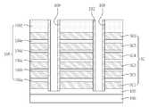
도 11 및 도 12i를 참조하면, 상기 도전막(133)을 이방성 식각하여, 게이트 분리 영역(127')을 형성할 수 있다. 상기 도전막(133)은 상기 희생막들(SC1~SC6)을 제거함으로써 형성되는 빈 공간에 잔존하여 도전성 패턴들(134a, 134b, 134c, 134d, 134e, 134f)을 형성할 수 있다. 상기 도전성 패턴들(134a, 134b, 134c, 134d, 134e, 134f)은 도전성 구조체(134)로 정의될 수 있다. 한편, 상기 층간 절연막들(106a~106b)은 층간 절연 패턴들(106a'~106f')로 정의될 수 있다.11 and 12I, the
상기 도전성 패턴들(134a~134f)은 상기 층간 절연 패턴들(106a'~106f')에 의해 서로 이격되면서 적층될 수 있다. 그리고, 상기 도전성 패턴들(106a'~106f')은 상기 층간 절연 패턴들(106a'~106f') 사이에 개재될 수 있다.The
본 실시예에서, 상기 층간 절연 패턴들(106a'~106f')로 이루어진 층간 절연 구조체(106')와 상기 도전성 패턴들(106a'~106f')로 이루어진 상기 도전성 구조체(134)는 수평 패턴들(135)로 정의할 수 있다. 따라서, 상기 수평 패턴들(135)은 상기 기판(100)의 상부 표면에 대하여 수평인 상기 도전성 패턴들(134a~134f) 및 상기 층간 절연 패턴들(106a'~106f')을 포함할 수 있다.
In the present exemplary embodiment, the
도 11 및 도 12j를 참조하면, 상기 게이트 분리 영역(127')을 채우는 게이트 분리 절연막(136)을 형성할 수 있다. 상기 게이트 분리 절연막(136)은 실리콘 산화막 등과 같은 절연성 물질로 형성할 수 있다. 상기 게이트 분리 절연막(136)을 형성하는 것은 상기 게이트 분리 영역(127')을 갖는 기판 상에 절연막을 형성하고, 상기 절연막을 평탄화하는 것을 포함할 수 있다. 한편, 상기 평탄화 공정 동안에, 상기 패드 패턴(124) 상의 게이트 절연막이 제거되어, 상기 패드 패턴(124)이 노출될 수 있다.11 and 12J, a gate
한편, 상기 반도체 패턴(112a) 및 상기 패드 패턴(124)을 갖는 기판 내에 불순물을 주입할 수 있다. 그 결과, 상기 패드 패턴(124)과 인접하는 상기 반도체 패턴(112a) 내에 제1 불순물 영역(D1)이 형성되고, 상기 패드 패턴(124) 내에 제2 불순물 영역(D2)이 형성될 수 있다. 상기 제1 및 제2 불순물 영역들(D1, D2)은 트랜지스터의 드레인 영역(D)을 구성할 수 있다. 상기 드레인 영역(D)은 고농도의 N+형일 수 있다.An impurity may be implanted into a substrate having the
한편, 도면에서 상기 드레인 영역(D)의 하부 경계를 점선으로 표시하였지만, 상기 드레인 영역(D)은 점선으로 표시된 경계에 한정되지 않는다. 예를 들어, 상기 드레인 영역(D)은 상기 패드 패턴(124)의 전체 영역에 걸쳐서 불순물 영역이 형성됨과 아울러 상기 패드 패턴(124)에 인접하는 상기 반도체 패턴(112a) 내에 불순물 영역이 형성될 수 있다.Meanwhile, although the lower boundary of the drain region D is indicated by a dotted line in the drawing, the drain region D is not limited to the boundary indicated by the dotted line. For example, in the drain region D, an impurity region may be formed over the entire area of the
한편, 상기 드레인 영역(D)은 게이트 분리 절연막(136)을 형성한 후에, 형성할 수 있지만, 이에 한정되지 않는다. 예를 들어, 상기 드레인 영역(D)은 도 12f에서와 같이 상기 패드 패턴(124)을 형성한 직후에 형성할 수도 있다.
The drain region D may be formed after the gate
도 11 및 도 12k를 참조하면, 상기 게이트 분리 절연막(136)을 갖는 기판 상에 상부 층간 절연막(139)을 형성할 수 있다. 상기 상부 층간 절연막(139)은 실리콘 산화막으로 형성할 수 있다. 상기 상부 층간 절연막(139)을 관통하며 상기 패드 패턴(124)과 전기적으로 연결된 비트라인 플러그(142)를 형성할 수 있다. 상기 상부 층간절연막(139) 상에 도전성 물질로 형성된 비트라인(145)을 형성할 수 있다. 한편, 상기 상부 층간 절연막(139)을 생략하고, 상기 비트라인(145)을 상기 패드 패턴(124)과 전기적으로 연결되도록 형성할 수도 있다.
11 and 12K, an upper
도 12a 내지 도 12k의 실시예에서 설명한 반도체 소자의 제조방법 중에서, 상기 반도체 패턴(112a)은 다른 형태로 변형되어 제조될 수 있다. 이하에서, 도 13a 내지 도 13b를 참조하여 도 12a 내지 도 12k의 실시예에서 변형된 부분에 대하여 설명하기로 한다.In the method of manufacturing the semiconductor device described with reference to FIGS. 12A through 12K, the
도 13a를 참조하면, 도 12c에서 설명한 상기 반도체 막(112)까지 형성된 기판을 준비할 수 있다. 이어서, 도 12d에서 설명한 상기 제1 갭필 패턴(115)를 형성하기 전에, 상기 반도체 막(112)을 이방성 식각할 수 있다. 그 결과, 상기 개구부(109)의 측벽 상에 잔존하는 반도체 패턴(212)이 형성될 수 있다.Referring to FIG. 13A, a substrate formed up to the
도 13b를 참조하면, 도 12d 내지 도 12e에서 설명한 것과 같은 방법으로 제1 및 제2 갭필 패턴들(115, 119)을 포함하는 갭필 구조체(121)를 형성하고, 도 12f에와 마찬가지로 패드 패턴(124)을 형성할 수 있다. 따라서, 도 12a 내지 도 12k의 실시예에서의 상기 반도체 패턴(112a)은 상기 갭필 구조체(121) 및 상기 패드 패턴들(124)의 측벽들을 둘러싸면서 상기 갭필 구조체(121)의 바닥면을 덮을 수 있는 반면에, 도 13b에서의 변형된 반도체 패턴(212)은 상기 갭필 구조체(121)의 바닥면을 덮지 않고, 상기 갭필 구조체(121) 및 상기 패드 패턴들(124)의 측벽들을 둘러싸도록 형성될 수 있다. 이어서, 도 12g 내지 도 12j에서 설명한 것과 같은 공정을 진행할 수 있다.
Referring to FIG. 13B, the
도 14a 내지 도 14d를 참조하여 본 발명의 또 다른 실시예에 따른 반도체소자의 제조방법에 대하여 설명하기로 한다.A method of manufacturing a semiconductor device according to still another embodiment of the present invention will be described with reference to FIGS. 14A through 14D.
도 14a를 참조하면, 도 12a에서와 같은 기판(300)이 제공될 수 있다. 상기 기판(300) 내에 불순물 영역(303)이 형성될 수 있다.Referring to FIG. 14A, a
상기 기판(300) 상에 버퍼 막(306)을 형성할 수 있다. 상기 버퍼 막(306)은 실리콘 산화막 및 고유전막 중 적어도 하나를 포함하는 절연막일 수 있다.A
상기 버퍼 막(306) 상에 도전성 막들(309a, 309b, 309b, 309c, 309e, 309f) 및 층간 절연막들(312a, 312b, 312c, 312d, 312e, 312f)을 교대로 형성할 수 있다. 따라서, 도전막 구조체(309)를 구성하는 상기 도전성 막들(309a~309f)은 상기 층간 절연막들(312a~312f)에 의해 서로 이격되면서 적층될 수 있다. 그리고, 상기 층간 절연막들(312a~312f)은 층간 절연 구조체(312)를 구성할 수 있다.
상기 도전성 막들(309a~309f)은 폴리실리콘 등과 같은 물질로 형성될 수 있다. 상기 층간 절연막들(312a~312f)은 실리콘 산화물, 실리콘 산질화물 또는 실리콘 질화물 등과 같은 절연성 물질로 형성될 수 있다. 상기 층간 절연막들(312a~312f) 중 최상부에 위치하는 층간절연막(312f)은 나머지 층간 절연막들(312a~312e) 각각의 두께보다 두꺼울 수 있다. 상기 층간 절연막들(312a~312f) 중 최상부에 위치하는 층간절연막(312f)의 두께가 상대적으로 두꺼운 이유는 후속 공정에서 형성될 패드 패턴이 형성될 공간을 확보하기 위함이다.The
도 14b를 참조하면, 상기 도전성 구조체(309) 및 상기 층간 절연 구조체(312)를 관통하는 개구부(315)를 형성할 수 있다. 상기 개구부(315)는 홀 형태일 수 있다.Referring to FIG. 14B, an
상기 개구부(315)의 측벽 상에 게이트 절연막(315)을 형성할 수 있다. 좀더 구체적으로, 상기 개구부(315)를 갖는 기판 상에 절연성 물질막을 형성하고, 상기 개구부(315)의 측벽 상에 잔존하면서 상기 개구부(315)의 바닥면에서의 상기 기판(300)이 노출되도록 상기 절연성 물질막을 식각하여 게이트 절연막(315)을 형성할 수 있다. 상기 게이트 절연막(315)은 도 2에서 설명한 것과 같이 터널 절연막, 정보 저장 막 및 블로킹 절연막을 포함할 수 있다.A
한편, 상기 게이트 절연막(315)을 형성한 후에, 상기 개구부(315)에 의해 노출된 상기 기판(300)을 식각하여 함몰 영역을 형성할 수도 있다. 즉, 상기 개구부(315)의 바닥 영역이 상기 기판(300)의 주표면 보다 아래에 위치하도록 형성할 수 있다.Meanwhile, after the
도 14c를 참조하면, 도 12c 내지 도 12f에서 설명한 상기 반도체 막(112)을 형성하는 공정부터 상기 패드 패턴(124)을 형성하는 공정을 상기 게이트 절연막(315)이 형성된 결과물에 대하여 수행할 수 있다. 그 결과, 상기 개구부(315) 내에 도 12f에서의 반도체 패턴(112a), 제1 및 제2 갭필 패턴들(115, 119)을 포함하는 갭필 구조체(121) 및 패드 패턴(124)에 각각 대응하는 반도체 패턴(319), 제1 및 제2 갭필 패턴들(321, 324)을 포함하는 갭필 구조체(327) 및 패드 패턴(330)이 형성될 수 있다. 도 12j에서 설명한 것과 같이, 상기 패드 패턴(330) 내에 그리고 상기 반도체 패턴(319) 내에 고농도의 불순물 영역(D)을 형성할 수 있다.Referring to FIG. 14C, the process of forming the
도 14d를 참조하면, 상기 도전성 구조체(309) 및 상기 층간 절연 구조체(312)를 패터닝하여, 도 12g에서 설명한 예비 게이트 분리 영역(127)에 대응하는 게이트 분리 영역(333)을 형성할 수 있다. 이어서, 상기 게이트 분리 영역(333)을 채우는 게이트 분리 절연막(336)을 형성할 수 있다. 상기 게이트 분리 절연막(336)은 실리콘 산화물 등과 같은 절연막으로 형성할 수 있다.Referring to FIG. 14D, the
따라서, 상기 게이트 분리 절연막(336)에 의해 상기 도전성 막들(309a~309f) 및 상기 층간 절연막들(312a~312f)은 각각 도전성 패턴들(309a'~309f') 및 층간 절연 패턴들(312a'~312f')로 정의될 수 있다. 상기 도전성 패턴들(309a'~309f')은 게이트 전극 구조체(312')로 정의하고, 상기 층간 절연 패턴들(312a'~312f')은 절연성 구조체(312')로 정의할 수 있다. 상기 도전성 패턴들(309a'~309f') 및 상기 층간 절연 패턴들(312a'~312f')은 수평 패턴들(313)로 정의할 수 있다.
Accordingly, the
다음으로, 도 15a 내지 도 15c를 참조하여 본 발명의 또 다른 실시예에 따른 반도체소자의 제조방법을 설명하기로 한다.Next, a method of manufacturing a semiconductor device according to still another embodiment of the present invention will be described with reference to FIGS. 15A to 15C.
도 15a를 참조하면, 도 14a에서 설명한 것과 같이 기판(400) 내에 불순물 영역(403)을 형성할 수 있다. 상기 기판(400) 상에 버퍼 막(406)을 형성할 수 있다. 상기 버퍼 막(406)은 실리콘 산화막 및 고유전막 중 적어도 하나를 포함하는 절연막일 수 있다.Referring to FIG. 15A, an
도 14a에서와 마찬가지로, 상기 버퍼 막(406) 상에 도전성 막들(409a, 409b, 409b, 409c, 409e, 409f) 및 층간 절연막들(412a, 412b, 412c, 412d, 412e, 412f)을 교대로 형성할 수 있다. 따라서, 도전막 구조체(409)를 구성하는 상기 도전성 막들(409a~409f)은 상기 층간 절연막들(412a~412f)에 의해 서로 이격되면서 적층될 수 있다. 그리고, 상기 층간 절연막들(412a~412f)은 층간 절연 구조체(412)를 구성할 수 있다.As in FIG. 14A,
상기 도전성 구조체(409) 및 상기 층간 절연 구조체(412)를 패터닝하여, 도 12g에서 설명한 예비 게이트 분리 영역(127)에 대응하는 게이트 분리 영역(415)을 형성할 수 있다. 상기 게이트 분리 영역(415)은, 평면도로 보았을 때, 라인 형상일 수 있다.The
상기 게이트 분리 영역(415)을 채우는 게이트 분리 절연막(418)을 형성할 수 있다. 상기 게이트 분리 절연막(418)은 실리콘 산화물 등과 같은 절연막으로 형성할 수 있다.A gate
상기 게이트 분리 절연막(418)을 갖는 기판 상에 상기 게이트 분리 절연막(418) 및 상기 층간 절연 구조체(412)를 덮는 캡핑 절연막(421)을 형성할 수 있다. 상기 캡핑 절연막(421)은 실리콘 질화물, 실리콘 산화 질화물 또는 실리콘 산화물 등과 같은 절연성 물질로 형성할 수 있다.A capping insulating
도 15b를 참조하면, 상기 캡핑 절연막(421), 상기 도전성 구조체(409) 및 상기 층간 절연 구조체(412)을 패터닝하여, 도 14b에서 설명한 상기 개구부(315)에 대응하는 개구부(424)를 형성할 수 있다.Referring to FIG. 15B, the capping insulating
상기 도전성 막들(409a~409f) 및 상기 층간 절연막들(412a~412f)은 상기 게이트 분리 절연막(418)에 의하여 라인 형상으로 정의된 도전성 패턴들(409a'~409f') 및 층간 절연 패턴들(412a'~412f')로 형성될 수 있다. 그리고, 상기 개구부(424)는 상기 도전성 패턴들(409a'~409f') 및 상기 층간 절연 패턴들(412a'~412f')을 수직적으로 관통하여 상기 기판(400)을 노출시킬 수 있다.The
도 15c를 참조하면, 도 14b에서와 같이 상기 개구부(424)의 측벽 상에 게이트 절연막(315)을 형성할 수 있다. 이어서, 도 12c 내지 도 12f에서 설명한 상기 반도체 막(112)을 형성하는 공정부터 상기 패드 패턴(124)을 형성하는 공정을 상기 게이트 절연막(424)이 형성된 결과물에 대하여 수행할 수 있다. 그 결과, 상기 개구부(424) 내에 도 12f에서의 반도체 패턴(112a), 제1 및 제2 갭필 패턴들(115, 119)을 포함하는 갭필 구조체(121) 및 패드 패턴(124)에 각각 대응하는 반도체 패턴(430), 제1 및 제2 갭필 패턴들(433, 436)을 포함하는 갭필 구조체(437) 및 패드 패턴(440)이 형성될 수 있다.Referring to FIG. 15C, as shown in FIG. 14B, a
상기 패드 패턴(440)을 갖는 기판 상에 상부 층간 절연막(443)을 형성할 수 있다. 상기 상부 층간 절연막(443)은 실리콘 산화막으로 형성할 수 있다. 상기 상부 층간 절연막(443)을 관통하며 상기 패드 패턴(440)과 전기적으로 연결된 비트라인 플러그(446)를 형성할 수 있다. 상기 상부 층간절연막(443) 상에 도전성 물질로 형성된 비트라인(449)을 형성할 수 있다. 한편, 상기 상부 층간 절연막(443)을 생략하고, 상기 비트라인(443)을 상기 패드 패턴(440)과 전기적으로 연결되도록 형성할 수도 있다.
An upper
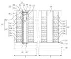
다음으로, 도 16 및 도 17a 내지 도 17e를 참조하여 본 발명의 또 다른 실시예에 따른 반도체소자의 제조방법을 설명하기로 한다. 도 17a 및 도 17e에서, 참조 부호 "G"로 표시된 부분은 도 16의 V-V'선을 따라 취해진 영역을 나타내고, 참조부호 "H"로 표시된 부분은 도 16의 VI-VI'선을 따라 취해진 영역을 나타낸다.Next, a method of manufacturing a semiconductor device according to still another embodiment of the present invention will be described with reference to FIGS. 16 and 17A to 17E. In Figs. 17A and 17E, the portion denoted by reference numeral "G" denotes an area taken along the line V-V 'of Fig. 16, and the portion denoted by reference numeral "H" is along the line VI-VI' of Fig. 16. Indicate the area taken.
도 16 및 도 17a를 참조하면, 도 12a에서와 같이 기판(500) 내에 불순물 영역(503)을 형성할 수 있다. 도 12a에서와 마찬가지로, 상기 기판(500) 상에 희생 막들(SC1, SC2, SC3, SC4, SC5, SC6) 및 층간 절연막들(506a, 506b, 506c, 506d, 506e, 506f)을 교대로 형성할 수 있다.16 and 17A, an
이어서, 상기 층간 절연막들(506a~506f) 및 상기 희생 막들(SC1~SC6)을 수직적으로 관통하며 가로지르는 라인 형상의 개구부(509)를 형성할 수 있다. 도 12a에서의 개구부(109)는 홀 형태이지만, 이번 실시예에서의 개구부(509)는 라인 형태일 수 있다.Subsequently, a line-shaped
도 16 및 도 17b를 참조하면, 상기 개구부(509)를 갖는 기판 상에 반도체 막(512)을 형성할 수 있다. 상기 반도체 막(512)은 결정질 실리콘 막으로 형성할 수 있다. 예를 들어, 상기 반도체 막(512)은 폴리 실리콘막으로 형성할 수 있다.16 and 17B, a
도 12d 내지 도 12e에서의 상기 제1 및 제2 갭필 패턴들(115, 119)을 형성하기 위한 공정과 동일한 공정을 진행하여, 상기 반도체 막(512) 상에 상기 개구부(509)를 부분적으로 채우는 제1 예비 갭필 패턴(515)을 형성하고, 상기 제1 예비 갭필 패턴(515) 상에 제2 예비 갭필 패턴(519)을 형성할 수 있다. 상기 제1 및 제2 예비 갭필 패턴들(515, 519)은 예비 갭필 구조체(521)로 정의할 수 있다.A process of forming the first and second
상기 예비 갭필 구조체(521)를 갖는 기판 상에 도전성 물질막을 형성하고, 상기 층간 절연막들(506a~506f) 중 최상부의 층간 절연막(506f)이 노출될 때까지 평탕화하여 패드 도전막(524)을 형성할 수 있다. 상기 패드 도전막(524)을 형성하기 위한 평탄화 공정 동안에, 상기 층간 절연막들(506a~506f) 중 최상부의 층간 절연막(506f) 상에 위치하는 반도체 막이 제거될 수 있다. 따라서, 상기 반도체 막(512)은 상기 개구부(509)의 측벽을 덮으면서 상기 예비 갭필 구조체(521)의 바닥면을 덮는 바닥부(512')를 가질 수 있다.A conductive material film is formed on the substrate having the preliminary
이어서, 상기 층간 절연막들(506a~506f) 및 상기 희생 막들(SC1~SC6)을 패터닝하여, 상기 개구부들(509) 사이에 위치하며 상기 기판(100)의 상부면을 노출시키는 예비 게이트 분리 영역(527)을 형성할 수 있다. 여기서, 상기 예비 게이트 분리 영역(527)은, 평면도로 보았을 때, 라인 형상일 수 있다.
Subsequently, the
도 16 및 도 17c를 참조하면, 상기 예비 게이트 분리 영역(527)가 형성된 결과물에 대하여, 도 12h에서 설명한 상기 희생 막들(SC1~SC6)을 제거하고, 상기 게이트 절연막(130)을 형성하고, 상기 도전막(133)을 형성하는 공정을 진행하고, 도 12i에서 설명한 상기 도전막(133)을 이방성 식각하는 공정을 진행하고, 도 12j에서 설명한 상기 게이트 분리 절연막(136)을 형성하는 공정을 진행할 수 있다. 그 결과, 상기 층간 절연막들(506a~506f)은 도 12j에서와 같이 층간 절연 패턴들(506')로 형성될 수 있고, 상기 희생 막들(SC1~SC6)이 제거된 결과물 상에 도 12h에서 설명한 것과 같은 게이트 절연막(530)이 형성될 수 있고, 도 12i에서 설명한 것과 같이 상기 희생 막들(SC1~SC6)이 제거되어 형성된 빈 공간에 도전성 패턴들(534)이 형성될 수 있다. 여기서, 상기 도전성 패턴들(534) 및 상기 층간 절연 패턴들(506')은 수평 패턴들(535)로 정의할 수 있다.Referring to FIGS. 16 and 17C, the sacrificial layers SC1 ˜ SC6 described with reference to FIG. 12H are removed and the
이어서, 도 12j에서 설명한 것과 같이 상기 예비 게이트 분리 영역(527)을 채우는 게이트 분리 절연막(536)을 형성할 수 있다.
Subsequently, as described with reference to FIG. 12J, a gate
도 17d를 참조하면, 라인 형상의 상기 개구부(509) 내에 형성된 상기 반도체 막(512), 상기 예비 갭필 구조체(521) 및 상기 패드 도전막(524)를 패터닝하여, 상기 개구부(509) 내에 반도체 패턴(512a), 갭필 구조체(521') 및 패드 패턴(524')을 각각 형성할 수 있다. 그리고, 상기 수평 패턴들(535) 사이에 그리고 상기 반도체 패턴(512a), 상기 갭필 구조체(521') 및 상기 패드 패턴(524')으로 이루어진 구조체들 사이에 빈 공간들(539)이 형성될 수 있다.Referring to FIG. 17D, the
상기 반도체 패턴(512a)은 상기 개구부(509)에 인접하는 상기 수평 패턴들(535)의 측벽을 따라 형성되며 상기 개구부(509)의 바닥면으로 연장된 바닥부(512a')를 가질 수 있다.The
상기 갭필 구조체(521')는 대향하는 양 측벽이 상기 반도체 패턴(512a)에 덮이며, 상기 반도체 패턴(512a)에 의해 덮이지 않은 상기 갭필 구조체(521')의 측벽들은 상기 빈 공간(539)에 의해 노출될 수 있다. 상기 갭필 구조체(521')는 앞의 실시예들, 특히 도 10a에서 설명한 것과 마찬가지로 제1 갭필 패턴(515') 및 제2 갭필 패턴(519')을 포함할 수 있다. 상기 패드 패턴(524')은 상기 갭필 구조체(521')의 상부면을 덮을 수 있다.
Opposite sidewalls of the
도 17e를 참조하면, 상기 빈 공간들(539)을 채우는 절연성 기둥들(542)을 형성할 수 있다. 상기 절연성 기둥들(542)은 상기 수평 패턴들(535) 사이에 위치함과 동시에 상기 반도체 패턴(512a), 상기 갭필 구조체(521') 및 상기 패드 패턴(524')으로 이루어진 구조체들 사이에 위치할 수 있다.
Referring to FIG. 17E, insulating
도 18은 본 발명의 실시예들에 따른 반도체 소자를 채택하는 전자 시스템(electronic system)의 개략적인 블록도이다. 상기 전자 시스템은 솔리드 스테이트 디스크(Solid State Disk; SSD; 810)와 같은 데이터 저장장치일 수 있다.18 is a schematic block diagram of an electronic system employing a semiconductor device in accordance with embodiments of the present invention. The electronic system may be a data storage device such as a solid state disk (SSD) 810.
도 18을 참조하면, 상기 솔리드 스테이트 디스크(SSD; 810)는 인터페이스(820), 제어기(controller; 830), 비휘발성 메모리(non-volatile memory; 840), 및 버퍼 메모리(buffer memory; 850)를 구비할 수 있다. 상기 비휘발성 메모리(non-volatile memory; 840)는 본 발명의 실시 예들 중 어느 하나의 실시예에 따라 제조된 소자일 수 있다.Referring to FIG. 18, the solid state disk (SSD) 810 may include an
상기 솔리드 스테이트 디스크(810)는 반도체를 이용하여 정보를 저장하는 장치이다. 상기 솔리드 스테이트 디스크(810)는 하드디스크드라이브(Hard Disk Drive; HDD)에 비하여 속도가 빠르고 기계적 지연이나 실패율, 발열ㅇ소음도 적으며, 소형화ㅇ경량화할 수 있는 장점이 있다. 상기 솔리드 스테이트 디스크(810)는 노트북PC, 데스크톱PC, MP3 플레이어, 또는 휴대용 저장장치에 사용될 수 있다.The
상기 제어기(830)는 상기 인터페이스(820)에 인접하게 형성되고 전기적으로 접속될 수 있다. 상기 제어기(830)는 메모리제어기 및 버퍼제어기를 구비할 수 있다. 상기 비휘발성 메모리(840)는 상기 제어기(830)에 인접하게 형성되고 전기적으로 접속될 수 있다. 상기 솔리드 스테이트 디스크(810)의 데이터 저장용량은 상기 비휘발성 메모리(840)에 대응할 수 있다. 상기 버퍼 메모리(850)는 상기 제어기(830)에 인접하게 형성되고 전기적으로 접속될 수 있다.The
상기 인터페이스(820)는 호스트(Host; 800)에 접속될 수 있으며 데이터와 같은 전기신호들을 송수신하는 역할을 할 수 있다. 예를 들면, 상기 인터페이스(820)는 SATA, IDE, SCSI, 및/또는 이들의 조합과 같은 규격을 사용하는 장치일 수 있다. 상기 비휘발성 메모리(840)는 상기 제어기(830)를 경유하여 상기 인터페이스(820)에 접속될 수 있다. 상기 비휘발성 메모리(840)는 상기 인터페이스(820)를 통하여 수신된 데이터를 저장하는 역할을 할 수 있다. 상기 솔리드 스테이트 디스크(810)에 전원공급이 차단된다 할지라도, 상기 비휘발성 메모리(840)에 저장된 데이터는 보존되는 특성이 있다.The
상기 버퍼 메모리(850)는 휘발성 메모리(volatile memory)를 구비할 수 있다. 상기 휘발성 메모리는 디램(Dynamic Random Access Memory; DRAM), 및/또는 에스램(Static Random Access Memory; SRAM)일 수 있다. 상기 버퍼 메모리(850)는 상기 비휘발성 메모리(840)에 비하여 상대적으로 빠른 동작속도를 보인다.The
상기 인터페이스(820)의 데이터 처리속도는 상기 비휘발성 메모리(840)의 동작속도에 비하여 상대적으로 빠를 수 있다. 여기서, 상기 버퍼 메모리(850)는 데이터를 임시 저장하는 역할을 할 수 있다. 상기 인터페이스(820)를 통하여 수신된 데이터는, 상기 제어기(830)를 경유하여 상기 버퍼 메모리(850)에 임시 저장된 후, 상기 비휘발성 메모리(840)의 데이터 기록(write) 속도에 맞추어 상기 비휘발성 메모리(840)에 영구 저장될 수 있다. 또한, 상기 비휘발성 메모리(840)에 저장된 데이터들 중 자주 사용되는 데이터들은 사전에 읽기(read) 하여 상기 버퍼 메모리(850)에 임시 저장할 수 있다. 즉, 상기 버퍼 메모리(850)는 상기 솔리드 스테이트 디스크(810)의 유효 동작속도를 증가시키고 에러(error) 발생률을 감소하는 역할을 할 수 있다.
The data processing speed of the
도 19는 본 발명의 실시예들에 따른 비휘발성 메모리 소자를 구비한 메모리 카드를 도시한 블록도이다.FIG. 19 is a block diagram illustrating a memory card including a nonvolatile memory device according to example embodiments. FIG.
도 19를 참조하면, 메모리 카드(1000; memory card)는 고용량의 데이터 저장 능력을 지원하기 위한 것으로 플래시 메모리(1010)를 포함한다. 플래시 메모리(1010)는 상술한 본 발명의 실시예들 중 어느 하나의 실시예에 따른 반도체 소자, 즉 비휘발성 메모리 소자를 포함할 수 있다. 예를 들어, 플래시 메모리(1010)는 상술한 본 발명의 실시예들 중 어느 하나의 실시예에 따른 낸드형 플래시 메모리 소자를 포함할 수 있다.Referring to FIG. 19, a memory card 1000 supports a high capacity data storage capability and includes a
메모리 카드(1000)는 호스트(HOST)와 플래시 메모리(1010:FALSH MEMORY) 사이의 제반 데이터 교환을 제어하는 메모리 컨트롤러(1020:MEMORY CONTROLLER)를 포함할 수 있다. 에스램(1021:SRAM)은 중앙처리장치(1022:CPU)의 동작 메모리로서 사용될 수 있다. 호스트 인터페이스(1023:HOST INTERFACE)는 메모리 카드(1000)와 접속되는 호스트(HOST)의 데이터 교환 프로토콜을 구비할 수 있다. 오류 수정 코드(1024:ECC)는 플래시 메모리(1010)로부터 독출된 데이터에 포함되는 오류를 검출 및 정정할 수 있다. 메모리 인터페이스(1025:MEMORY INTERFACE)는 플래시 메모리(1010)와 인터페이싱 할 수 있다. 중앙처리장치(1022)는 메모리 컨트롤러(1020)의 데이터 교환을 위한 제반제어 동작을 수행한다. 비록 도면에는 도시되지 않았지만, 메모리 카드(1000)는 호스트(HOST)와의 인터페이싱을 위한 코드 데이터를 저장하는 롬(ROM)을 더 포함할 수 있다.
The memory card 1000 may include a
도 20은 본 발명 실시예에 따른 정보 처리 시스템을 도시한 블록도이다.20 is a block diagram illustrating an information processing system according to an embodiment of the present invention.
도 20을 참조하면, 정보 처리 시스템(1100)은 본 발명의 실시예들 중 어느 하나의 실시예에 따른 비휘발성 메모리 소자, 일례로 플래시 메모리 소자(예: 낸드 플래시 메모리 소자)를 구비한 플래시 메모리 시스템(1110)을 포함할 수 있다.Referring to FIG. 20, an
정보처리 시스템(1100)은 모바일 기기나 컴퓨터 등을 포함할 수 있다. 예를 들어, 정보 처리 시스템(1100)은 플래시 메모리 시스템(1110)과 각각 시스템 버스(1160)에 전기적으로 연결된 모뎀(1120:MODEM), 중앙처리장치(1130:CPU), 램(1140:RAM), 유저 인터페이스(1150:USER INTERFACE)를 포함할 수 있다. 플래시 메모리 시스템(1110)에는 중앙처리장치(1130)에 의해서 처리된 데이터 또는 외부에서 입력된 데이터가 저장될 수 있다.The
정보 처리 시스템(1100)은 메모리 카드, 반도체 디스크 장치(Solid State Disk), 카메라 이미지 프로세서(Camera Image Sensor) 및 그 밖의 응용 칩셋(Application Chipset)으로 제공될 수 있다. 예를 들어, 플래시 메모리 시스템(1110)은 반도체 디스크 장치(SSD)로 구성될 수 있으며, 이 경우 정보 처리 시스템(1100)은 대용량의 데이터를 플래시 메모리 시스템(1110)에 안정적으로 그리고 신뢰성있게 저장할 수 있다.The
본 발명의 실시예들 중 어느 하나의 실시예에 따른 플래시 메모리 또는 플래시 메모리 시스템은 다양한 형태의 패키지로 실장될 수 있다. 예를 들면, 본 발명에 따른 플래시 메모리 또는 플래시 메모리 시스템은 패키지 온 패키지(Package on Package), 볼 그리드 어레이(Ball Grid Arrays), 칩 스케일 패키지(Chip scale packages), 플라스틱 리드 칩 캐리어(Plastic Leaded Chip Carrier), 플라스틱 듀얼 인라인 패키지(Plastic Dual In-Line Package), 멀티 칩 패키지(Multi Chip Package), 웨이퍼 레벨 패키지(Wafer Level Package), 웨이퍼 레벨 제조 패키지(Wafer Level Fabricated Package), 웨이퍼 레벨 프로세스 스택 패키지(Wafer Level Processed Stack Package), 다이 온 와플 패키지(Die On Waffle Package), 다이 인 웨이퍼 폼(Die in Wafer Form), 칩 온 보오드(Chip On Board), 세라믹 듀얼 인라인 패키지(Ceramic Dual In-Line Package), 플라스킥 메트릭 쿼드 플랫 패키지(Plastic Metric Quad Flat Pack), 씬 쿼드 플랫 패키지(Thin Quad Flat Pack), 스몰 아웃라인 패키지(Small Outline Package), 축소 스몰 아웃라인 패키지(Shrink Small Outline Package), 씬 스몰 아웃라인 패키지(Thin Small Outline Package), 씬쿼드 플랫 패키지(Thin Quad Flat Package), 시스템 인 패키지(System In Package) 등과 같은 방식으로 패키징될 수 있다.
The flash memory or the flash memory system according to any one of the embodiments of the present invention may be mounted in various types of packages. For example, a flash memory or flash memory system according to the present invention may be a package on package, a ball grid array, chip scale packages, a plastic leaded chip. Carrier, Plastic Dual In-Line Package, Multi Chip Package, Wafer Level Package, Wafer Level Fabricated Package, Wafer Level Process Stack Package (Wafer Level Processed Stack Package), Die On Waffle Package, Die in Wafer Form, Chip On Board, Ceramic Dual In-Line Package ), Plastic Metric Quad Flat Pack, Thin Quad Flat Pack, Small Outline Package, Collapsible Square The package may be packaged in a manner such as a mall small outline package, a thin small outline package, a thin quad flat package, a system in package, or the like. .
이상 첨부된 도면을 참조하여 본 발명의 실시예들을 개략적으로 설명하였지만, 본 발명이 속하는 기술분야에서 통상의 지식을 가진 자는 본 발명이 그 기술적 사상이나 필수적인 특징을 변경하지 않고서 다른 구체적인 형태로 실시될 수 있다는 것을 이해할 수 있을 것이다. 그러므로 이상에서 기술한 실시예들은 모든 면에서 예시적인 것이며 한정적이 아닌 것으로 이해하여야 한다.While the embodiments of the present invention have been schematically described with reference to the accompanying drawings, those skilled in the art to which the present invention pertains may be embodied in other specific forms without changing the technical spirit or essential features of the present invention. I can understand that you can. It is therefore to be understood that the above-described embodiments are illustrative in all aspects and not restrictive.
Claims (10)
Translated fromKorean상기 개구부의 상부 영역 내에 제공된 패드 패턴;
상기 패드 패턴과 상기 기판 사이의 상기 개구부 내에 제공되며, 제1 및 제2 갭필 패턴들을 포함하는 절연성의 갭필 구조체; 및
상기 갭필 구조체의 측벽과 상기 수평 패턴들의 측벽들 사이, 및 상기 패드 패턴의 측벽과 상기 수평 패턴들의 측벽들 사이에 형성된 반도체 패턴을 포함하되,
상기 제1 갭필 패턴은 제1 산화물을 포함하고,
상기 제2 갭필 패턴은 상기 제1 산화물과 다른 식각 선택비를 갖는 제2 산화물을 포함하는 반도체 소자.Horizontal patterns provided on the substrate and having one or a plurality of openings;
A pad pattern provided in an upper region of the opening;
An insulating gapfill structure provided in the opening between the pad pattern and the substrate, the insulating gapfill structure comprising first and second gapfill patterns; And
A semiconductor pattern formed between the sidewall of the gapfill structure and the sidewalls of the horizontal patterns, and between the sidewall of the pad pattern and the sidewalls of the horizontal patterns,
The first gap fill pattern includes a first oxide,
The second gap fill pattern may include a second oxide having an etching selectivity different from that of the first oxide.
상기 반도체 패턴으로부터 연장되어 상기 갭필 구조체와 상기 기판 사이에 개재된 반도체 패턴의 바닥 부(bottom portion)를 더 포함하는 반도체소자.The method of claim 1,
And a bottom portion of the semiconductor pattern extending from the semiconductor pattern and interposed between the gap fill structure and the substrate.
상기 제1 갭필 패턴은 상부면의 가운데 부분이 오목하게 함몰된 모양이고,
상기 제2 갭필 패턴은 상기 제1 갭필 패턴과 상기 패드 패턴 사이에 개재된 반도체 소자.The method of claim 1,
The first gap fill pattern has a shape in which a center portion of the upper surface is concavely recessed,
The second gap fill pattern is a semiconductor device interposed between the first gap fill pattern and the pad pattern.
상기 제2 갭필 패턴은 기둥 모양이고,
상기 제1 갭필 패턴은 상기 제2 갭필 패턴의 측벽을 둘러싸는 반도체소자.The method of claim 1,
The second gap fill pattern is a columnar shape,
The first gap fill pattern may surround sidewalls of the second gap fill pattern.
상기 수평 패턴들은 복수의 도전성 패턴들과 복수의 절연 패턴들이 교대로 적층되어 형성되되,
상기 수평 패턴들의 최상층은 절연 패턴이고,
상기 도전성 패턴들 중 최하부에 위치한 도전성 패턴은 상기 기판과 이격된 반도체 소자.The method of claim 1,
The horizontal patterns are formed by alternately stacking a plurality of conductive patterns and a plurality of insulating patterns,
The uppermost layer of the horizontal patterns is an insulating pattern,
The conductive pattern positioned on the lowermost of the conductive patterns is spaced apart from the substrate.
상기 도전성 패턴들과 상기 반도체 패턴 사이에 개재된 게이트 절연막을 더 포함하는 반도체 소자.The method of claim 5, wherein
The semiconductor device further comprises a gate insulating layer interposed between the conductive patterns and the semiconductor pattern.
상기 수평 패턴들을 관통하며 상기 기판을 노출시키는 하나 또는 복수의 개구부;
상기 개구부의 상부 영역 내에 제공되며 결정질 실리콘을 포함하는 패드 패턴;
상기 패드 패턴과 상기 반도체 기판 사이의 상기 개구부 내에 제공되며, 제1 산화물을 포함하는 제1 갭필 패턴 및 상기 제1 산화물과 다른 식각 선택비를 갖는 제2 산화물을 포함하는 제2 갭필 패턴을 포함하는 갭필 구조체;
상기 갭필 구조체의 측벽과 상기 수평 패턴들의 측벽들 사이 및 상기 패드 패턴과 상기 수평 패턴들의 측벽들 사이에 형성되며, 결정질 실리콘을 포함하는 반도체 패턴;
상기 패드 패턴 및 상기 패드 패턴과 인접하는 상기 반도체 패턴 내에 제공된 불순물 영역; 및
상기 반도체 패턴과 상기 게이트 전극들 사이에 형성되며, 정보 저장 막을 갖는 게이트 절연막을 포함하는 반도체 소자.Horizontal patterns provided on the semiconductor substrate and including alternately stacked gate electrodes and insulating patterns;
One or more openings through the horizontal patterns and exposing the substrate;
A pad pattern provided in an upper region of the opening and including crystalline silicon;
A second gap fill pattern provided in the opening between the pad pattern and the semiconductor substrate and including a first gap fill pattern including a first oxide and a second oxide having an etching selectivity different from that of the first oxide; Gapfill structures;
A semiconductor pattern formed between the sidewalls of the gapfill structure and the sidewalls of the horizontal patterns and between the pad pattern and the sidewalls of the horizontal patterns, the semiconductor pattern comprising crystalline silicon;
An impurity region provided in the pad pattern and the semiconductor pattern adjacent to the pad pattern; And
And a gate insulating film formed between the semiconductor pattern and the gate electrodes and having an information storage film.
상기 개구부 내에서, 상기 도전성 패턴들의 측벽들은 상기 절연성 패턴들의 측벽들과 수직 정렬 되지 않는 반도체 소자.The method of claim 7, wherein
Within the opening, sidewalls of the conductive patterns are not vertically aligned with sidewalls of the insulating patterns.
상기 개구부 내에서, 상기 도전성 패턴들의 측벽들은 상기 절연성 패턴들의 측벽들과 수직 정렬된 반도체 소자.The method of claim 7, wherein
Within the opening, sidewalls of the conductive patterns are vertically aligned with sidewalls of the insulating patterns.
상기 개구부의 측벽을 덮는 반도체 패턴을 형성하고,
상기 반도체 패턴을 갖는 기판 상에 제1 산화물을 포함하는 제1 예비 갭필 막을 형성하고,
상기 제1 예비 갭필 막을 부분 식각하여 상기 개구부를 부분적으로 채우는 제1 갭필 패턴을 형성하고,
상기 제1 갭필 패턴을 갖는 기판 상에 제2 산화물을 포함하는 제2 예비 갭필 막을 형성하되, 상기 제2 산화물은 상기 제1 산화물에 비하여 식각 속도가 빠른 산화물로 형성되고,
상기 개구부의 상부 영역에 위치하는 상기 반도체 패턴의 측벽이 노출되도록 상기 제2 예비 갭필 막을 부분 식각하여 제2 갭필 패턴을 형성하고,
상기 제2 갭필 패턴 상에 상기 개구부의 나머지 부분을 채우며 상기 반도체 패턴과 전기적으로 연결되는 패드 패턴을 형성하는 것을 포함하는 방법에 의해 제조된 반도체소자.Forming a structure having an opening on the substrate,
Forming a semiconductor pattern covering sidewalls of the openings;
Forming a first preliminary gapfill film including a first oxide on the substrate having the semiconductor pattern,
Partially etching the first preliminary gapfill film to form a first gapfill pattern partially filling the opening;
Forming a second preliminary gapfill film including a second oxide on the substrate having the first gapfill pattern, wherein the second oxide is formed of an oxide having a faster etching rate than that of the first oxide,
Forming a second gap fill pattern by partially etching the second preliminary gap fill layer to expose sidewalls of the semiconductor pattern positioned in an upper region of the opening;
And forming a pad pattern on the second gap fill pattern, the pad pattern filling the remaining portion of the opening and electrically connected to the semiconductor pattern.
Priority Applications (2)
| Application Number | Priority Date | Filing Date | Title |
|---|---|---|---|
| KR1020100091300AKR20120029291A (en) | 2010-09-16 | 2010-09-16 | Semiconductor devices and methods of fabricating the same |
| US13/234,534US20120068242A1 (en) | 2010-09-16 | 2011-09-16 | Semiconductor devices and methods of fabricating the same |
Applications Claiming Priority (1)
| Application Number | Priority Date | Filing Date | Title |
|---|---|---|---|
| KR1020100091300AKR20120029291A (en) | 2010-09-16 | 2010-09-16 | Semiconductor devices and methods of fabricating the same |
Publications (1)
| Publication Number | Publication Date |
|---|---|
| KR20120029291Atrue KR20120029291A (en) | 2012-03-26 |
Family
ID=45816961
Family Applications (1)
| Application Number | Title | Priority Date | Filing Date |
|---|---|---|---|
| KR1020100091300AWithdrawnKR20120029291A (en) | 2010-09-16 | 2010-09-16 | Semiconductor devices and methods of fabricating the same |
Country Status (2)
| Country | Link |
|---|---|
| US (1) | US20120068242A1 (en) |
| KR (1) | KR20120029291A (en) |
Cited By (6)
| Publication number | Priority date | Publication date | Assignee | Title |
|---|---|---|---|---|
| WO2014098992A1 (en)* | 2012-12-17 | 2014-06-26 | Intel Corporation | Three dimensional memory |
| US9129859B2 (en) | 2013-03-06 | 2015-09-08 | Intel Corporation | Three dimensional memory structure |
| US9343469B2 (en) | 2012-06-27 | 2016-05-17 | Intel Corporation | Three dimensional NAND flash with self-aligned select gate |
| US10319678B2 (en) | 2014-09-26 | 2019-06-11 | Intel Corporation | Capping poly channel pillars in stacked circuits |
| US11018149B2 (en) | 2014-03-27 | 2021-05-25 | Intel Corporation | Building stacked hollow channels for a three dimensional circuit device |
| US11626414B2 (en) | 2019-09-30 | 2023-04-11 | Samsung Electronics Co., Ltd. | Three-dimensional semiconductor memory devices and methods of fabricating the same |
Families Citing this family (537)
| Publication number | Priority date | Publication date | Assignee | Title |
|---|---|---|---|---|
| US9299568B2 (en) | 2007-05-25 | 2016-03-29 | Cypress Semiconductor Corporation | SONOS ONO stack scaling |
| US8614124B2 (en) | 2007-05-25 | 2013-12-24 | Cypress Semiconductor Corporation | SONOS ONO stack scaling |
| US9431549B2 (en) | 2007-12-12 | 2016-08-30 | Cypress Semiconductor Corporation | Nonvolatile charge trap memory device having a high dielectric constant blocking region |
| US10378106B2 (en) | 2008-11-14 | 2019-08-13 | Asm Ip Holding B.V. | Method of forming insulation film by modified PEALD |
| US9394608B2 (en) | 2009-04-06 | 2016-07-19 | Asm America, Inc. | Semiconductor processing reactor and components thereof |
| US9102522B2 (en) | 2009-04-24 | 2015-08-11 | Cypress Semiconductor Corporation | Method of ONO integration into logic CMOS flow |
| US8071453B1 (en) | 2009-04-24 | 2011-12-06 | Cypress Semiconductor Corporation | Method of ONO integration into MOS flow |
| US8802201B2 (en) | 2009-08-14 | 2014-08-12 | Asm America, Inc. | Systems and methods for thin-film deposition of metal oxides using excited nitrogen-oxygen species |
| US9324576B2 (en) | 2010-05-27 | 2016-04-26 | Applied Materials, Inc. | Selective etch for silicon films |
| US10283321B2 (en) | 2011-01-18 | 2019-05-07 | Applied Materials, Inc. | Semiconductor processing system and methods using capacitively coupled plasma |
| US9064815B2 (en) | 2011-03-14 | 2015-06-23 | Applied Materials, Inc. | Methods for etch of metal and metal-oxide films |
| US8999856B2 (en) | 2011-03-14 | 2015-04-07 | Applied Materials, Inc. | Methods for etch of sin films |
| KR101794017B1 (en)* | 2011-05-12 | 2017-11-06 | 삼성전자 주식회사 | Nonvolatile memory device and and fabricating method thereof |
| US9312155B2 (en) | 2011-06-06 | 2016-04-12 | Asm Japan K.K. | High-throughput semiconductor-processing apparatus equipped with multiple dual-chamber modules |
| US10364496B2 (en) | 2011-06-27 | 2019-07-30 | Asm Ip Holding B.V. | Dual section module having shared and unshared mass flow controllers |
| US10854498B2 (en) | 2011-07-15 | 2020-12-01 | Asm Ip Holding B.V. | Wafer-supporting device and method for producing same |
| US20130023129A1 (en) | 2011-07-20 | 2013-01-24 | Asm America, Inc. | Pressure transmitter for a semiconductor processing environment |
| KR101964085B1 (en)* | 2011-07-26 | 2019-07-31 | 삼성전자 주식회사 | Non-volatile memory device and method for fabricating the device |
| JP2013030557A (en) | 2011-07-27 | 2013-02-07 | Elpida Memory Inc | Method of manufacturing semiconductor device |
| US8771536B2 (en) | 2011-08-01 | 2014-07-08 | Applied Materials, Inc. | Dry-etch for silicon-and-carbon-containing films |
| US8927390B2 (en) | 2011-09-26 | 2015-01-06 | Applied Materials, Inc. | Intrench profile |
| US8808563B2 (en) | 2011-10-07 | 2014-08-19 | Applied Materials, Inc. | Selective etch of silicon by way of metastable hydrogen termination |
| US9017481B1 (en) | 2011-10-28 | 2015-04-28 | Asm America, Inc. | Process feed management for semiconductor substrate processing |
| EP2831918A4 (en)* | 2012-03-29 | 2015-11-18 | Cypress Semiconductor Corp | ONO INTEGRATION METHOD IN LOGICAL CMOS FLOW |
| US9267739B2 (en) | 2012-07-18 | 2016-02-23 | Applied Materials, Inc. | Pedestal with multi-zone temperature control and multiple purge capabilities |
| US9373517B2 (en) | 2012-08-02 | 2016-06-21 | Applied Materials, Inc. | Semiconductor processing with DC assisted RF power for improved control |
| US9659799B2 (en) | 2012-08-28 | 2017-05-23 | Asm Ip Holding B.V. | Systems and methods for dynamic semiconductor process scheduling |
| US9021985B2 (en) | 2012-09-12 | 2015-05-05 | Asm Ip Holdings B.V. | Process gas management for an inductively-coupled plasma deposition reactor |
| US9034770B2 (en) | 2012-09-17 | 2015-05-19 | Applied Materials, Inc. | Differential silicon oxide etch |
| US9023734B2 (en) | 2012-09-18 | 2015-05-05 | Applied Materials, Inc. | Radical-component oxide etch |
| US9390937B2 (en) | 2012-09-20 | 2016-07-12 | Applied Materials, Inc. | Silicon-carbon-nitride selective etch |
| US9132436B2 (en) | 2012-09-21 | 2015-09-15 | Applied Materials, Inc. | Chemical control features in wafer process equipment |
| US10714315B2 (en) | 2012-10-12 | 2020-07-14 | Asm Ip Holdings B.V. | Semiconductor reaction chamber showerhead |
| US8969212B2 (en) | 2012-11-20 | 2015-03-03 | Applied Materials, Inc. | Dry-etch selectivity |
| KR101934426B1 (en)* | 2012-11-26 | 2019-01-03 | 삼성전자 주식회사 | Semiconductor device and method for fabricating the same |
| US9064816B2 (en) | 2012-11-30 | 2015-06-23 | Applied Materials, Inc. | Dry-etch for selective oxidation removal |
| US8980763B2 (en) | 2012-11-30 | 2015-03-17 | Applied Materials, Inc. | Dry-etch for selective tungsten removal |
| US9111877B2 (en) | 2012-12-18 | 2015-08-18 | Applied Materials, Inc. | Non-local plasma oxide etch |
| US8921234B2 (en) | 2012-12-21 | 2014-12-30 | Applied Materials, Inc. | Selective titanium nitride etching |
| US20160376700A1 (en) | 2013-02-01 | 2016-12-29 | Asm Ip Holding B.V. | System for treatment of deposition reactor |
| US10256079B2 (en) | 2013-02-08 | 2019-04-09 | Applied Materials, Inc. | Semiconductor processing systems having multiple plasma configurations |
| US9362130B2 (en) | 2013-03-01 | 2016-06-07 | Applied Materials, Inc. | Enhanced etching processes using remote plasma sources |
| US9040422B2 (en) | 2013-03-05 | 2015-05-26 | Applied Materials, Inc. | Selective titanium nitride removal |
| US8801952B1 (en) | 2013-03-07 | 2014-08-12 | Applied Materials, Inc. | Conformal oxide dry etch |
| US9484191B2 (en) | 2013-03-08 | 2016-11-01 | Asm Ip Holding B.V. | Pulsed remote plasma method and system |
| US10170282B2 (en) | 2013-03-08 | 2019-01-01 | Applied Materials, Inc. | Insulated semiconductor faceplate designs |
| US9589770B2 (en) | 2013-03-08 | 2017-03-07 | Asm Ip Holding B.V. | Method and systems for in-situ formation of intermediate reactive species |
| US9449982B2 (en) | 2013-03-12 | 2016-09-20 | Sandisk Technologies Llc | Method of making a vertical NAND device using a sacrificial layer with air gap and sequential etching of multilayer stacks |
| US8946023B2 (en) | 2013-03-12 | 2015-02-03 | Sandisk Technologies Inc. | Method of making a vertical NAND device using sequential etching of multilayer stacks |
| US9230987B2 (en) | 2014-02-20 | 2016-01-05 | Sandisk Technologies Inc. | Multilevel memory stack structure and methods of manufacturing the same |
| US9515080B2 (en) | 2013-03-12 | 2016-12-06 | Sandisk Technologies Llc | Vertical NAND and method of making thereof using sequential stack etching and landing pad |
| US9698153B2 (en) | 2013-03-12 | 2017-07-04 | Sandisk Technologies Llc | Vertical NAND and method of making thereof using sequential stack etching and self-aligned landing pad |
| US20140271097A1 (en) | 2013-03-15 | 2014-09-18 | Applied Materials, Inc. | Processing systems and methods for halide scavenging |
| US9276011B2 (en) | 2013-03-15 | 2016-03-01 | Micron Technology, Inc. | Cell pillar structures and integrated flows |
| US8895449B1 (en) | 2013-05-16 | 2014-11-25 | Applied Materials, Inc. | Delicate dry clean |
| US9114438B2 (en) | 2013-05-21 | 2015-08-25 | Applied Materials, Inc. | Copper residue chamber clean |
| US9493879B2 (en) | 2013-07-12 | 2016-11-15 | Applied Materials, Inc. | Selective sputtering for pattern transfer |
| US9773648B2 (en) | 2013-08-30 | 2017-09-26 | Applied Materials, Inc. | Dual discharge modes operation for remote plasma |
| US8956980B1 (en) | 2013-09-16 | 2015-02-17 | Applied Materials, Inc. | Selective etch of silicon nitride |
| US9240412B2 (en) | 2013-09-27 | 2016-01-19 | Asm Ip Holding B.V. | Semiconductor structure and device and methods of forming same using selective epitaxial process |
| US8951429B1 (en) | 2013-10-29 | 2015-02-10 | Applied Materials, Inc. | Tungsten oxide processing |
| US9437604B2 (en) | 2013-11-01 | 2016-09-06 | Micron Technology, Inc. | Methods and apparatuses having strings of memory cells including a metal source |
| US9431410B2 (en)* | 2013-11-01 | 2016-08-30 | Micron Technology, Inc. | Methods and apparatuses having memory cells including a monolithic semiconductor channel |
| US9576809B2 (en) | 2013-11-04 | 2017-02-21 | Applied Materials, Inc. | Etch suppression with germanium |
| US9236265B2 (en) | 2013-11-04 | 2016-01-12 | Applied Materials, Inc. | Silicon germanium processing |
| US9520303B2 (en) | 2013-11-12 | 2016-12-13 | Applied Materials, Inc. | Aluminum selective etch |
| US9245762B2 (en) | 2013-12-02 | 2016-01-26 | Applied Materials, Inc. | Procedure for etch rate consistency |
| US9117855B2 (en) | 2013-12-04 | 2015-08-25 | Applied Materials, Inc. | Polarity control for remote plasma |
| US9287095B2 (en) | 2013-12-17 | 2016-03-15 | Applied Materials, Inc. | Semiconductor system assemblies and methods of operation |
| US9263278B2 (en) | 2013-12-17 | 2016-02-16 | Applied Materials, Inc. | Dopant etch selectivity control |
| US9190293B2 (en) | 2013-12-18 | 2015-11-17 | Applied Materials, Inc. | Even tungsten etch for high aspect ratio trenches |
| EP2887396B1 (en) | 2013-12-20 | 2017-03-08 | Imec | Three-dimensional resistive memory array |
| US9287134B2 (en) | 2014-01-17 | 2016-03-15 | Applied Materials, Inc. | Titanium oxide etch |
| US9293568B2 (en) | 2014-01-27 | 2016-03-22 | Applied Materials, Inc. | Method of fin patterning |
| US9396989B2 (en) | 2014-01-27 | 2016-07-19 | Applied Materials, Inc. | Air gaps between copper lines |
| US9385028B2 (en) | 2014-02-03 | 2016-07-05 | Applied Materials, Inc. | Air gap process |
| US10683571B2 (en) | 2014-02-25 | 2020-06-16 | Asm Ip Holding B.V. | Gas supply manifold and method of supplying gases to chamber using same |
| US9499898B2 (en) | 2014-03-03 | 2016-11-22 | Applied Materials, Inc. | Layered thin film heater and method of fabrication |
| US9299575B2 (en) | 2014-03-17 | 2016-03-29 | Applied Materials, Inc. | Gas-phase tungsten etch |
| US10167557B2 (en) | 2014-03-18 | 2019-01-01 | Asm Ip Holding B.V. | Gas distribution system, reactor including the system, and methods of using the same |
| US11015245B2 (en) | 2014-03-19 | 2021-05-25 | Asm Ip Holding B.V. | Gas-phase reactor and system having exhaust plenum and components thereof |
| US9299538B2 (en) | 2014-03-20 | 2016-03-29 | Applied Materials, Inc. | Radial waveguide systems and methods for post-match control of microwaves |
| US9299537B2 (en) | 2014-03-20 | 2016-03-29 | Applied Materials, Inc. | Radial waveguide systems and methods for post-match control of microwaves |
| US9136273B1 (en) | 2014-03-21 | 2015-09-15 | Applied Materials, Inc. | Flash gate air gap |
| US9903020B2 (en) | 2014-03-31 | 2018-02-27 | Applied Materials, Inc. | Generation of compact alumina passivation layers on aluminum plasma equipment components |
| US9269590B2 (en) | 2014-04-07 | 2016-02-23 | Applied Materials, Inc. | Spacer formation |
| WO2015159414A1 (en)* | 2014-04-17 | 2015-10-22 | ユニサンティス エレクトロニクス シンガポール プライベート リミテッド | Columnar semiconductor memory device and method for manufacturing same |
| US9309598B2 (en) | 2014-05-28 | 2016-04-12 | Applied Materials, Inc. | Oxide and metal removal |
| US9847289B2 (en) | 2014-05-30 | 2017-12-19 | Applied Materials, Inc. | Protective via cap for improved interconnect performance |
| US9583505B2 (en) | 2014-06-05 | 2017-02-28 | Kabushiki Kaisha Toshiba | Non-volatile memory device |
| JP5889486B1 (en)* | 2014-06-10 | 2016-03-22 | ユニサンティス エレクトロニクス シンガポール プライベート リミテッドUnisantis Electronics Singapore Pte Ltd. | Columnar semiconductor memory device and manufacturing method thereof |
| US9378969B2 (en) | 2014-06-19 | 2016-06-28 | Applied Materials, Inc. | Low temperature gas-phase carbon removal |
| US9406523B2 (en) | 2014-06-19 | 2016-08-02 | Applied Materials, Inc. | Highly selective doped oxide removal method |
| US9425058B2 (en) | 2014-07-24 | 2016-08-23 | Applied Materials, Inc. | Simplified litho-etch-litho-etch process |
| US10858737B2 (en) | 2014-07-28 | 2020-12-08 | Asm Ip Holding B.V. | Showerhead assembly and components thereof |
| US9496167B2 (en) | 2014-07-31 | 2016-11-15 | Applied Materials, Inc. | Integrated bit-line airgap formation and gate stack post clean |
| US9378978B2 (en) | 2014-07-31 | 2016-06-28 | Applied Materials, Inc. | Integrated oxide recess and floating gate fin trimming |
| US9159606B1 (en) | 2014-07-31 | 2015-10-13 | Applied Materials, Inc. | Metal air gap |
| US9165786B1 (en) | 2014-08-05 | 2015-10-20 | Applied Materials, Inc. | Integrated oxide and nitride recess for better channel contact in 3D architectures |
| US9659753B2 (en) | 2014-08-07 | 2017-05-23 | Applied Materials, Inc. | Grooved insulator to reduce leakage current |
| US9553102B2 (en) | 2014-08-19 | 2017-01-24 | Applied Materials, Inc. | Tungsten separation |
| US9890456B2 (en) | 2014-08-21 | 2018-02-13 | Asm Ip Holding B.V. | Method and system for in situ formation of gas-phase compounds |
| KR102330391B1 (en)* | 2014-09-11 | 2021-11-24 | 삼성전자주식회사 | Storage device, data storage system having the same, and garbage collection method thereof |
| US9355856B2 (en) | 2014-09-12 | 2016-05-31 | Applied Materials, Inc. | V trench dry etch |
| US9368364B2 (en) | 2014-09-24 | 2016-06-14 | Applied Materials, Inc. | Silicon etch process with tunable selectivity to SiO2 and other materials |
| US9355862B2 (en) | 2014-09-24 | 2016-05-31 | Applied Materials, Inc. | Fluorine-based hardmask removal |
| US9613822B2 (en) | 2014-09-25 | 2017-04-04 | Applied Materials, Inc. | Oxide etch selectivity enhancement |
| US10941490B2 (en) | 2014-10-07 | 2021-03-09 | Asm Ip Holding B.V. | Multiple temperature range susceptor, assembly, reactor and system including the susceptor, and methods of using the same |
| US9657845B2 (en) | 2014-10-07 | 2017-05-23 | Asm Ip Holding B.V. | Variable conductance gas distribution apparatus and method |
| US9966240B2 (en) | 2014-10-14 | 2018-05-08 | Applied Materials, Inc. | Systems and methods for internal surface conditioning assessment in plasma processing equipment |
| US9355922B2 (en) | 2014-10-14 | 2016-05-31 | Applied Materials, Inc. | Systems and methods for internal surface conditioning in plasma processing equipment |
| US11637002B2 (en) | 2014-11-26 | 2023-04-25 | Applied Materials, Inc. | Methods and systems to enhance process uniformity |
| US9299583B1 (en) | 2014-12-05 | 2016-03-29 | Applied Materials, Inc. | Aluminum oxide selective etch |
| US10573496B2 (en) | 2014-12-09 | 2020-02-25 | Applied Materials, Inc. | Direct outlet toroidal plasma source |
| US10224210B2 (en) | 2014-12-09 | 2019-03-05 | Applied Materials, Inc. | Plasma processing system with direct outlet toroidal plasma source |
| KR102263121B1 (en) | 2014-12-22 | 2021-06-09 | 에이에스엠 아이피 홀딩 비.브이. | Semiconductor device and manufacuring method thereof |
| US9502258B2 (en) | 2014-12-23 | 2016-11-22 | Applied Materials, Inc. | Anisotropic gap etch |
| US9343272B1 (en) | 2015-01-08 | 2016-05-17 | Applied Materials, Inc. | Self-aligned process |
| US11257693B2 (en) | 2015-01-09 | 2022-02-22 | Applied Materials, Inc. | Methods and systems to improve pedestal temperature control |
| US9373522B1 (en) | 2015-01-22 | 2016-06-21 | Applied Mateials, Inc. | Titanium nitride removal |
| US9449846B2 (en) | 2015-01-28 | 2016-09-20 | Applied Materials, Inc. | Vertical gate separation |
| US20160225652A1 (en) | 2015-02-03 | 2016-08-04 | Applied Materials, Inc. | Low temperature chuck for plasma processing systems |
| US9728437B2 (en) | 2015-02-03 | 2017-08-08 | Applied Materials, Inc. | High temperature chuck for plasma processing systems |
| US9881805B2 (en) | 2015-03-02 | 2018-01-30 | Applied Materials, Inc. | Silicon selective removal |
| US10529542B2 (en) | 2015-03-11 | 2020-01-07 | Asm Ip Holdings B.V. | Cross-flow reactor and method |
| US10276355B2 (en) | 2015-03-12 | 2019-04-30 | Asm Ip Holding B.V. | Multi-zone reactor, system including the reactor, and method of using the same |
| US9627403B2 (en) | 2015-04-30 | 2017-04-18 | Sandisk Technologies Llc | Multilevel memory stack structure employing support pillar structures |
| KR102282139B1 (en)* | 2015-05-12 | 2021-07-28 | 삼성전자주식회사 | Semiconductor devices |
| US10458018B2 (en) | 2015-06-26 | 2019-10-29 | Asm Ip Holding B.V. | Structures including metal carbide material, devices including the structures, and methods of forming same |
| US10600673B2 (en) | 2015-07-07 | 2020-03-24 | Asm Ip Holding B.V. | Magnetic susceptor to baseplate seal |
| US10083836B2 (en) | 2015-07-24 | 2018-09-25 | Asm Ip Holding B.V. | Formation of boron-doped titanium metal films with high work function |
| US9741593B2 (en) | 2015-08-06 | 2017-08-22 | Applied Materials, Inc. | Thermal management systems and methods for wafer processing systems |
| US9691645B2 (en) | 2015-08-06 | 2017-06-27 | Applied Materials, Inc. | Bolted wafer chuck thermal management systems and methods for wafer processing systems |
| US9349605B1 (en) | 2015-08-07 | 2016-05-24 | Applied Materials, Inc. | Oxide etch selectivity systems and methods |
| US9761599B2 (en) | 2015-08-17 | 2017-09-12 | Micron Technology, Inc. | Integrated structures containing vertically-stacked memory cells |
| US9853043B2 (en) | 2015-08-25 | 2017-12-26 | Sandisk Technologies Llc | Method of making a multilevel memory stack structure using a cavity containing a sacrificial fill material |
| US9502471B1 (en) | 2015-08-25 | 2016-11-22 | Sandisk Technologies Llc | Multi tier three-dimensional memory devices including vertically shared bit lines |
| US10504700B2 (en) | 2015-08-27 | 2019-12-10 | Applied Materials, Inc. | Plasma etching systems and methods with secondary plasma injection |
| US9842853B2 (en)* | 2015-09-14 | 2017-12-12 | Toshiba Memory Corporation | Memory cell array with improved substrate current pathway |
| US9960072B2 (en) | 2015-09-29 | 2018-05-01 | Asm Ip Holding B.V. | Variable adjustment for precise matching of multiple chamber cavity housings |
| US10211308B2 (en) | 2015-10-21 | 2019-02-19 | Asm Ip Holding B.V. | NbMC layers |
| US10322384B2 (en) | 2015-11-09 | 2019-06-18 | Asm Ip Holding B.V. | Counter flow mixer for process chamber |
| CN106711149B (en)* | 2015-11-12 | 2019-07-12 | 旺宏电子股份有限公司 | Vertical channel structure |
| US11139308B2 (en) | 2015-12-29 | 2021-10-05 | Asm Ip Holding B.V. | Atomic layer deposition of III-V compounds to form V-NAND devices |
| US10468251B2 (en) | 2016-02-19 | 2019-11-05 | Asm Ip Holding B.V. | Method for forming spacers using silicon nitride film for spacer-defined multiple patterning |
| US10529554B2 (en) | 2016-02-19 | 2020-01-07 | Asm Ip Holding B.V. | Method for forming silicon nitride film selectively on sidewalls or flat surfaces of trenches |
| US10501866B2 (en) | 2016-03-09 | 2019-12-10 | Asm Ip Holding B.V. | Gas distribution apparatus for improved film uniformity in an epitaxial system |
| US10343920B2 (en) | 2016-03-18 | 2019-07-09 | Asm Ip Holding B.V. | Aligned carbon nanotubes |
| US9892913B2 (en) | 2016-03-24 | 2018-02-13 | Asm Ip Holding B.V. | Radial and thickness control via biased multi-port injection settings |
| US10190213B2 (en) | 2016-04-21 | 2019-01-29 | Asm Ip Holding B.V. | Deposition of metal borides |
| US10865475B2 (en) | 2016-04-21 | 2020-12-15 | Asm Ip Holding B.V. | Deposition of metal borides and silicides |
| US10032628B2 (en) | 2016-05-02 | 2018-07-24 | Asm Ip Holding B.V. | Source/drain performance through conformal solid state doping |
| US10367080B2 (en) | 2016-05-02 | 2019-07-30 | Asm Ip Holding B.V. | Method of forming a germanium oxynitride film |
| KR102592471B1 (en) | 2016-05-17 | 2023-10-20 | 에이에스엠 아이피 홀딩 비.브이. | Method of forming metal interconnection and method of fabricating semiconductor device using the same |
| US10522371B2 (en) | 2016-05-19 | 2019-12-31 | Applied Materials, Inc. | Systems and methods for improved semiconductor etching and component protection |
| US10504754B2 (en) | 2016-05-19 | 2019-12-10 | Applied Materials, Inc. | Systems and methods for improved semiconductor etching and component protection |
| US11453943B2 (en) | 2016-05-25 | 2022-09-27 | Asm Ip Holding B.V. | Method for forming carbon-containing silicon/metal oxide or nitride film by ALD using silicon precursor and hydrocarbon precursor |
| US10388509B2 (en) | 2016-06-28 | 2019-08-20 | Asm Ip Holding B.V. | Formation of epitaxial layers via dislocation filtering |
| US9865484B1 (en) | 2016-06-29 | 2018-01-09 | Applied Materials, Inc. | Selective etch using material modification and RF pulsing |
| US9859151B1 (en) | 2016-07-08 | 2018-01-02 | Asm Ip Holding B.V. | Selective film deposition method to form air gaps |
| US10612137B2 (en) | 2016-07-08 | 2020-04-07 | Asm Ip Holdings B.V. | Organic reactants for atomic layer deposition |
| US10714385B2 (en) | 2016-07-19 | 2020-07-14 | Asm Ip Holding B.V. | Selective deposition of tungsten |
| KR102354490B1 (en) | 2016-07-27 | 2022-01-21 | 에이에스엠 아이피 홀딩 비.브이. | Method of processing a substrate |
| US10395919B2 (en) | 2016-07-28 | 2019-08-27 | Asm Ip Holding B.V. | Method and apparatus for filling a gap |
| US9887082B1 (en) | 2016-07-28 | 2018-02-06 | Asm Ip Holding B.V. | Method and apparatus for filling a gap |
| US9812320B1 (en) | 2016-07-28 | 2017-11-07 | Asm Ip Holding B.V. | Method and apparatus for filling a gap |
| KR102532607B1 (en) | 2016-07-28 | 2023-05-15 | 에이에스엠 아이피 홀딩 비.브이. | Substrate processing apparatus and method of operating the same |
| US10062575B2 (en) | 2016-09-09 | 2018-08-28 | Applied Materials, Inc. | Poly directional etch by oxidation |
| US10629473B2 (en) | 2016-09-09 | 2020-04-21 | Applied Materials, Inc. | Footing removal for nitride spacer |
| US10546729B2 (en) | 2016-10-04 | 2020-01-28 | Applied Materials, Inc. | Dual-channel showerhead with improved profile |
| US10062585B2 (en) | 2016-10-04 | 2018-08-28 | Applied Materials, Inc. | Oxygen compatible plasma source |
| US9721789B1 (en) | 2016-10-04 | 2017-08-01 | Applied Materials, Inc. | Saving ion-damaged spacers |
| US9934942B1 (en) | 2016-10-04 | 2018-04-03 | Applied Materials, Inc. | Chamber with flow-through source |
| US10062579B2 (en) | 2016-10-07 | 2018-08-28 | Applied Materials, Inc. | Selective SiN lateral recess |
| US9947549B1 (en) | 2016-10-10 | 2018-04-17 | Applied Materials, Inc. | Cobalt-containing material removal |
| US10410943B2 (en) | 2016-10-13 | 2019-09-10 | Asm Ip Holding B.V. | Method for passivating a surface of a semiconductor and related systems |
| US10643826B2 (en) | 2016-10-26 | 2020-05-05 | Asm Ip Holdings B.V. | Methods for thermally calibrating reaction chambers |
| US9881929B1 (en) | 2016-10-27 | 2018-01-30 | Sandisk Technologies Llc | Multi-tier memory stack structure containing non-overlapping support pillar structures and method of making thereof |
| US11532757B2 (en) | 2016-10-27 | 2022-12-20 | Asm Ip Holding B.V. | Deposition of charge trapping layers |
| US10229833B2 (en) | 2016-11-01 | 2019-03-12 | Asm Ip Holding B.V. | Methods for forming a transition metal nitride film on a substrate by atomic layer deposition and related semiconductor device structures |
| US10714350B2 (en) | 2016-11-01 | 2020-07-14 | ASM IP Holdings, B.V. | Methods for forming a transition metal niobium nitride film on a substrate by atomic layer deposition and related semiconductor device structures |
| US10643904B2 (en) | 2016-11-01 | 2020-05-05 | Asm Ip Holdings B.V. | Methods for forming a semiconductor device and related semiconductor device structures |
| US10435790B2 (en) | 2016-11-01 | 2019-10-08 | Asm Ip Holding B.V. | Method of subatmospheric plasma-enhanced ALD using capacitively coupled electrodes with narrow gap |
| US10134757B2 (en) | 2016-11-07 | 2018-11-20 | Asm Ip Holding B.V. | Method of processing a substrate and a device manufactured by using the method |
| US10163696B2 (en) | 2016-11-11 | 2018-12-25 | Applied Materials, Inc. | Selective cobalt removal for bottom up gapfill |
| US9768034B1 (en) | 2016-11-11 | 2017-09-19 | Applied Materials, Inc. | Removal methods for high aspect ratio structures |
| US10242908B2 (en) | 2016-11-14 | 2019-03-26 | Applied Materials, Inc. | Airgap formation with damage-free copper |
| US10026621B2 (en) | 2016-11-14 | 2018-07-17 | Applied Materials, Inc. | SiN spacer profile patterning |
| KR102546317B1 (en) | 2016-11-15 | 2023-06-21 | 에이에스엠 아이피 홀딩 비.브이. | Gas supply unit and substrate processing apparatus including the same |
| US10340135B2 (en) | 2016-11-28 | 2019-07-02 | Asm Ip Holding B.V. | Method of topologically restricted plasma-enhanced cyclic deposition of silicon or metal nitride |
| KR102762543B1 (en) | 2016-12-14 | 2025-02-05 | 에이에스엠 아이피 홀딩 비.브이. | Substrate processing apparatus |
| US11447861B2 (en) | 2016-12-15 | 2022-09-20 | Asm Ip Holding B.V. | Sequential infiltration synthesis apparatus and a method of forming a patterned structure |
| US11581186B2 (en) | 2016-12-15 | 2023-02-14 | Asm Ip Holding B.V. | Sequential infiltration synthesis apparatus |
| KR102700194B1 (en) | 2016-12-19 | 2024-08-28 | 에이에스엠 아이피 홀딩 비.브이. | Substrate processing apparatus |
| US10056399B2 (en) | 2016-12-22 | 2018-08-21 | Sandisk Technologies Llc | Three-dimensional memory devices containing inter-tier dummy memory cells and methods of making the same |
| US10269558B2 (en) | 2016-12-22 | 2019-04-23 | Asm Ip Holding B.V. | Method of forming a structure on a substrate |
| US10566206B2 (en) | 2016-12-27 | 2020-02-18 | Applied Materials, Inc. | Systems and methods for anisotropic material breakthrough |
| US10867788B2 (en) | 2016-12-28 | 2020-12-15 | Asm Ip Holding B.V. | Method of forming a structure on a substrate |
| US11390950B2 (en) | 2017-01-10 | 2022-07-19 | Asm Ip Holding B.V. | Reactor system and method to reduce residue buildup during a film deposition process |
| US10403507B2 (en) | 2017-02-03 | 2019-09-03 | Applied Materials, Inc. | Shaped etch profile with oxidation |
| US10431429B2 (en) | 2017-02-03 | 2019-10-01 | Applied Materials, Inc. | Systems and methods for radial and azimuthal control of plasma uniformity |
| US10043684B1 (en) | 2017-02-06 | 2018-08-07 | Applied Materials, Inc. | Self-limiting atomic thermal etching systems and methods |
| US10319739B2 (en) | 2017-02-08 | 2019-06-11 | Applied Materials, Inc. | Accommodating imperfectly aligned memory holes |
| US10655221B2 (en) | 2017-02-09 | 2020-05-19 | Asm Ip Holding B.V. | Method for depositing oxide film by thermal ALD and PEALD |
| US10468261B2 (en) | 2017-02-15 | 2019-11-05 | Asm Ip Holding B.V. | Methods for forming a metallic film on a substrate by cyclical deposition and related semiconductor device structures |
| US10943834B2 (en) | 2017-03-13 | 2021-03-09 | Applied Materials, Inc. | Replacement contact process |
| US10529563B2 (en) | 2017-03-29 | 2020-01-07 | Asm Ip Holdings B.V. | Method for forming doped metal oxide films on a substrate by cyclical deposition and related semiconductor device structures |
| US10283353B2 (en) | 2017-03-29 | 2019-05-07 | Asm Ip Holding B.V. | Method of reforming insulating film deposited on substrate with recess pattern |
| US10319649B2 (en) | 2017-04-11 | 2019-06-11 | Applied Materials, Inc. | Optical emission spectroscopy (OES) for remote plasma monitoring |
| KR102457289B1 (en) | 2017-04-25 | 2022-10-21 | 에이에스엠 아이피 홀딩 비.브이. | Method for depositing a thin film and manufacturing a semiconductor device |
| US10770286B2 (en) | 2017-05-08 | 2020-09-08 | Asm Ip Holdings B.V. | Methods for selectively forming a silicon nitride film on a substrate and related semiconductor device structures |
| US10446393B2 (en) | 2017-05-08 | 2019-10-15 | Asm Ip Holding B.V. | Methods for forming silicon-containing epitaxial layers and related semiconductor device structures |
| US10892156B2 (en) | 2017-05-08 | 2021-01-12 | Asm Ip Holding B.V. | Methods for forming a silicon nitride film on a substrate and related semiconductor device structures |
| US20180331117A1 (en) | 2017-05-12 | 2018-11-15 | Sandisk Technologies Llc | Multilevel memory stack structure with tapered inter-tier joint region and methods of making thereof |
| US11276590B2 (en) | 2017-05-17 | 2022-03-15 | Applied Materials, Inc. | Multi-zone semiconductor substrate supports |
| JP7176860B6 (en) | 2017-05-17 | 2022-12-16 | アプライド マテリアルズ インコーポレイテッド | Semiconductor processing chamber to improve precursor flow |
| US11276559B2 (en) | 2017-05-17 | 2022-03-15 | Applied Materials, Inc. | Semiconductor processing chamber for multiple precursor flow |
| US10497579B2 (en) | 2017-05-31 | 2019-12-03 | Applied Materials, Inc. | Water-free etching methods |
| US10049891B1 (en) | 2017-05-31 | 2018-08-14 | Applied Materials, Inc. | Selective in situ cobalt residue removal |
| US10504742B2 (en) | 2017-05-31 | 2019-12-10 | Asm Ip Holding B.V. | Method of atomic layer etching using hydrogen plasma |
| US10886123B2 (en) | 2017-06-02 | 2021-01-05 | Asm Ip Holding B.V. | Methods for forming low temperature semiconductor layers and related semiconductor device structures |
| US10920320B2 (en) | 2017-06-16 | 2021-02-16 | Applied Materials, Inc. | Plasma health determination in semiconductor substrate processing reactors |
| US12040200B2 (en) | 2017-06-20 | 2024-07-16 | Asm Ip Holding B.V. | Semiconductor processing apparatus and methods for calibrating a semiconductor processing apparatus |
| US10541246B2 (en) | 2017-06-26 | 2020-01-21 | Applied Materials, Inc. | 3D flash memory cells which discourage cross-cell electrical tunneling |
| US11306395B2 (en) | 2017-06-28 | 2022-04-19 | Asm Ip Holding B.V. | Methods for depositing a transition metal nitride film on a substrate by atomic layer deposition and related deposition apparatus |
| US10685834B2 (en) | 2017-07-05 | 2020-06-16 | Asm Ip Holdings B.V. | Methods for forming a silicon germanium tin layer and related semiconductor device structures |
| US10727080B2 (en) | 2017-07-07 | 2020-07-28 | Applied Materials, Inc. | Tantalum-containing material removal |
| US10541184B2 (en) | 2017-07-11 | 2020-01-21 | Applied Materials, Inc. | Optical emission spectroscopic techniques for monitoring etching |
| US10354889B2 (en) | 2017-07-17 | 2019-07-16 | Applied Materials, Inc. | Non-halogen etching of silicon-containing materials |
| KR20190009245A (en) | 2017-07-18 | 2019-01-28 | 에이에스엠 아이피 홀딩 비.브이. | Methods for forming a semiconductor device structure and related semiconductor device structures |
| US10541333B2 (en) | 2017-07-19 | 2020-01-21 | Asm Ip Holding B.V. | Method for depositing a group IV semiconductor and related semiconductor device structures |
| US11018002B2 (en) | 2017-07-19 | 2021-05-25 | Asm Ip Holding B.V. | Method for selectively depositing a Group IV semiconductor and related semiconductor device structures |
| US11374112B2 (en) | 2017-07-19 | 2022-06-28 | Asm Ip Holding B.V. | Method for depositing a group IV semiconductor and related semiconductor device structures |
| US10312055B2 (en) | 2017-07-26 | 2019-06-04 | Asm Ip Holding B.V. | Method of depositing film by PEALD using negative bias |
| US10605530B2 (en) | 2017-07-26 | 2020-03-31 | Asm Ip Holding B.V. | Assembly of a liner and a flange for a vertical furnace as well as the liner and the vertical furnace |
| US10590535B2 (en) | 2017-07-26 | 2020-03-17 | Asm Ip Holdings B.V. | Chemical treatment, deposition and/or infiltration apparatus and method for using the same |
| TWI815813B (en) | 2017-08-04 | 2023-09-21 | 荷蘭商Asm智慧財產控股公司 | Showerhead assembly for distributing a gas within a reaction chamber |
| US10170336B1 (en) | 2017-08-04 | 2019-01-01 | Applied Materials, Inc. | Methods for anisotropic control of selective silicon removal |
| US10043674B1 (en) | 2017-08-04 | 2018-08-07 | Applied Materials, Inc. | Germanium etching systems and methods |
| US10297458B2 (en) | 2017-08-07 | 2019-05-21 | Applied Materials, Inc. | Process window widening using coated parts in plasma etch processes |
| US10692741B2 (en) | 2017-08-08 | 2020-06-23 | Asm Ip Holdings B.V. | Radiation shield |
| US10770336B2 (en) | 2017-08-08 | 2020-09-08 | Asm Ip Holding B.V. | Substrate lift mechanism and reactor including same |
| US11139191B2 (en) | 2017-08-09 | 2021-10-05 | Asm Ip Holding B.V. | Storage apparatus for storing cassettes for substrates and processing apparatus equipped therewith |
| US10249524B2 (en) | 2017-08-09 | 2019-04-02 | Asm Ip Holding B.V. | Cassette holder assembly for a substrate cassette and holding member for use in such assembly |
| US11769682B2 (en) | 2017-08-09 | 2023-09-26 | Asm Ip Holding B.V. | Storage apparatus for storing cassettes for substrates and processing apparatus equipped therewith |
| US10236177B1 (en) | 2017-08-22 | 2019-03-19 | ASM IP Holding B.V.. | Methods for depositing a doped germanium tin semiconductor and related semiconductor device structures |
| USD900036S1 (en) | 2017-08-24 | 2020-10-27 | Asm Ip Holding B.V. | Heater electrical connector and adapter |
| US11830730B2 (en) | 2017-08-29 | 2023-11-28 | Asm Ip Holding B.V. | Layer forming method and apparatus |
| US11056344B2 (en) | 2017-08-30 | 2021-07-06 | Asm Ip Holding B.V. | Layer forming method |
| KR102491945B1 (en) | 2017-08-30 | 2023-01-26 | 에이에스엠 아이피 홀딩 비.브이. | Substrate processing apparatus |
| US11295980B2 (en) | 2017-08-30 | 2022-04-05 | Asm Ip Holding B.V. | Methods for depositing a molybdenum metal film over a dielectric surface of a substrate by a cyclical deposition process and related semiconductor device structures |
| KR102401446B1 (en) | 2017-08-31 | 2022-05-24 | 에이에스엠 아이피 홀딩 비.브이. | Substrate processing apparatus |
| US10607895B2 (en) | 2017-09-18 | 2020-03-31 | Asm Ip Holdings B.V. | Method for forming a semiconductor device structure comprising a gate fill metal |
| KR102630301B1 (en) | 2017-09-21 | 2024-01-29 | 에이에스엠 아이피 홀딩 비.브이. | Method of sequential infiltration synthesis treatment of infiltrateable material and structures and devices formed using same |
| US10844484B2 (en) | 2017-09-22 | 2020-11-24 | Asm Ip Holding B.V. | Apparatus for dispensing a vapor phase reactant to a reaction chamber and related methods |
| US10658205B2 (en) | 2017-09-28 | 2020-05-19 | Asm Ip Holdings B.V. | Chemical dispensing apparatus and methods for dispensing a chemical to a reaction chamber |
| US10403504B2 (en) | 2017-10-05 | 2019-09-03 | Asm Ip Holding B.V. | Method for selectively depositing a metallic film on a substrate |
| US10319588B2 (en) | 2017-10-10 | 2019-06-11 | Asm Ip Holding B.V. | Method for depositing a metal chalcogenide on a substrate by cyclical deposition |
| US10128086B1 (en) | 2017-10-24 | 2018-11-13 | Applied Materials, Inc. | Silicon pretreatment for nitride removal |
| US10283324B1 (en) | 2017-10-24 | 2019-05-07 | Applied Materials, Inc. | Oxygen treatment for nitride etching |
| US10923344B2 (en) | 2017-10-30 | 2021-02-16 | Asm Ip Holding B.V. | Methods for forming a semiconductor structure and related semiconductor structures |
| KR102443047B1 (en) | 2017-11-16 | 2022-09-14 | 에이에스엠 아이피 홀딩 비.브이. | Method of processing a substrate and a device manufactured by the same |
| US10910262B2 (en) | 2017-11-16 | 2021-02-02 | Asm Ip Holding B.V. | Method of selectively depositing a capping layer structure on a semiconductor device structure |
| US11022879B2 (en) | 2017-11-24 | 2021-06-01 | Asm Ip Holding B.V. | Method of forming an enhanced unexposed photoresist layer |
| CN111344522B (en) | 2017-11-27 | 2022-04-12 | 阿斯莫Ip控股公司 | Including clean mini-environment device |
| WO2019103613A1 (en) | 2017-11-27 | 2019-05-31 | Asm Ip Holding B.V. | A storage device for storing wafer cassettes for use with a batch furnace |
| US10290508B1 (en) | 2017-12-05 | 2019-05-14 | Asm Ip Holding B.V. | Method for forming vertical spacers for spacer-defined patterning |
| US10256112B1 (en) | 2017-12-08 | 2019-04-09 | Applied Materials, Inc. | Selective tungsten removal |
| US10903054B2 (en) | 2017-12-19 | 2021-01-26 | Applied Materials, Inc. | Multi-zone gas distribution systems and methods |
| US11328909B2 (en) | 2017-12-22 | 2022-05-10 | Applied Materials, Inc. | Chamber conditioning and removal processes |
| US10854426B2 (en) | 2018-01-08 | 2020-12-01 | Applied Materials, Inc. | Metal recess for semiconductor structures |
| US10872771B2 (en) | 2018-01-16 | 2020-12-22 | Asm Ip Holding B. V. | Method for depositing a material film on a substrate within a reaction chamber by a cyclical deposition process and related device structures |
| US10283493B1 (en) | 2018-01-17 | 2019-05-07 | Sandisk Technologies Llc | Three-dimensional memory device containing bonded memory die and peripheral logic die and method of making thereof |
| US10510738B2 (en) | 2018-01-17 | 2019-12-17 | Sandisk Technologies Llc | Three-dimensional memory device having support-die-assisted source power distribution and method of making thereof |
| TWI799494B (en) | 2018-01-19 | 2023-04-21 | 荷蘭商Asm 智慧財產控股公司 | Deposition method |
| KR102695659B1 (en) | 2018-01-19 | 2024-08-14 | 에이에스엠 아이피 홀딩 비.브이. | Method for depositing a gap filling layer by plasma assisted deposition |
| USD903477S1 (en) | 2018-01-24 | 2020-12-01 | Asm Ip Holdings B.V. | Metal clamp |
| US11018047B2 (en) | 2018-01-25 | 2021-05-25 | Asm Ip Holding B.V. | Hybrid lift pin |
| US10535516B2 (en) | 2018-02-01 | 2020-01-14 | Asm Ip Holdings B.V. | Method for depositing a semiconductor structure on a surface of a substrate and related semiconductor structures |
| USD880437S1 (en) | 2018-02-01 | 2020-04-07 | Asm Ip Holding B.V. | Gas supply plate for semiconductor manufacturing apparatus |
| US11081345B2 (en) | 2018-02-06 | 2021-08-03 | Asm Ip Holding B.V. | Method of post-deposition treatment for silicon oxide film |
| WO2019158960A1 (en) | 2018-02-14 | 2019-08-22 | Asm Ip Holding B.V. | A method for depositing a ruthenium-containing film on a substrate by a cyclical deposition process |
| US10896820B2 (en) | 2018-02-14 | 2021-01-19 | Asm Ip Holding B.V. | Method for depositing a ruthenium-containing film on a substrate by a cyclical deposition process |
| US10731249B2 (en) | 2018-02-15 | 2020-08-04 | Asm Ip Holding B.V. | Method of forming a transition metal containing film on a substrate by a cyclical deposition process, a method for supplying a transition metal halide compound to a reaction chamber, and related vapor deposition apparatus |
| US10964512B2 (en) | 2018-02-15 | 2021-03-30 | Applied Materials, Inc. | Semiconductor processing chamber multistage mixing apparatus and methods |
| US10679870B2 (en) | 2018-02-15 | 2020-06-09 | Applied Materials, Inc. | Semiconductor processing chamber multistage mixing apparatus |
| KR102636427B1 (en) | 2018-02-20 | 2024-02-13 | 에이에스엠 아이피 홀딩 비.브이. | Substrate processing method and apparatus |
| US10658181B2 (en) | 2018-02-20 | 2020-05-19 | Asm Ip Holding B.V. | Method of spacer-defined direct patterning in semiconductor fabrication |
| US10975470B2 (en) | 2018-02-23 | 2021-04-13 | Asm Ip Holding B.V. | Apparatus for detecting or monitoring for a chemical precursor in a high temperature environment |
| TWI766433B (en) | 2018-02-28 | 2022-06-01 | 美商應用材料股份有限公司 | Systems and methods to form airgaps |
| US11473195B2 (en) | 2018-03-01 | 2022-10-18 | Asm Ip Holding B.V. | Semiconductor processing apparatus and a method for processing a substrate |
| US10593560B2 (en) | 2018-03-01 | 2020-03-17 | Applied Materials, Inc. | Magnetic induction plasma source for semiconductor processes and equipment |
| US11629406B2 (en) | 2018-03-09 | 2023-04-18 | Asm Ip Holding B.V. | Semiconductor processing apparatus comprising one or more pyrometers for measuring a temperature of a substrate during transfer of the substrate |
| US10319600B1 (en) | 2018-03-12 | 2019-06-11 | Applied Materials, Inc. | Thermal silicon etch |
| US10497573B2 (en) | 2018-03-13 | 2019-12-03 | Applied Materials, Inc. | Selective atomic layer etching of semiconductor materials |
| US11114283B2 (en) | 2018-03-16 | 2021-09-07 | Asm Ip Holding B.V. | Reactor, system including the reactor, and methods of manufacturing and using same |
| KR102646467B1 (en) | 2018-03-27 | 2024-03-11 | 에이에스엠 아이피 홀딩 비.브이. | Method of forming an electrode on a substrate and a semiconductor device structure including an electrode |
| US11230766B2 (en) | 2018-03-29 | 2022-01-25 | Asm Ip Holding B.V. | Substrate processing apparatus and method |
| US10510536B2 (en) | 2018-03-29 | 2019-12-17 | Asm Ip Holding B.V. | Method of depositing a co-doped polysilicon film on a surface of a substrate within a reaction chamber |
| US11088002B2 (en) | 2018-03-29 | 2021-08-10 | Asm Ip Holding B.V. | Substrate rack and a substrate processing system and method |
| KR102501472B1 (en) | 2018-03-30 | 2023-02-20 | 에이에스엠 아이피 홀딩 비.브이. | Substrate processing method |
| US10573527B2 (en) | 2018-04-06 | 2020-02-25 | Applied Materials, Inc. | Gas-phase selective etching systems and methods |
| KR102600229B1 (en) | 2018-04-09 | 2023-11-10 | 에이에스엠 아이피 홀딩 비.브이. | Substrate supporting device, substrate processing apparatus including the same and substrate processing method |
| US10490406B2 (en) | 2018-04-10 | 2019-11-26 | Appled Materials, Inc. | Systems and methods for material breakthrough |
| US10699879B2 (en) | 2018-04-17 | 2020-06-30 | Applied Materials, Inc. | Two piece electrode assembly with gap for plasma control |
| US10381322B1 (en) | 2018-04-23 | 2019-08-13 | Sandisk Technologies Llc | Three-dimensional memory device containing self-aligned interlocking bonded structure and method of making the same |
| US10886137B2 (en) | 2018-04-30 | 2021-01-05 | Applied Materials, Inc. | Selective nitride removal |
| TWI811348B (en) | 2018-05-08 | 2023-08-11 | 荷蘭商Asm 智慧財產控股公司 | Methods for depositing an oxide film on a substrate by a cyclical deposition process and related device structures |
| US12025484B2 (en) | 2018-05-08 | 2024-07-02 | Asm Ip Holding B.V. | Thin film forming method |
| US12272527B2 (en) | 2018-05-09 | 2025-04-08 | Asm Ip Holding B.V. | Apparatus for use with hydrogen radicals and method of using same |
| KR20190129718A (en) | 2018-05-11 | 2019-11-20 | 에이에스엠 아이피 홀딩 비.브이. | Methods for forming a doped metal carbide film on a substrate and related semiconductor device structures |
| KR102596988B1 (en) | 2018-05-28 | 2023-10-31 | 에이에스엠 아이피 홀딩 비.브이. | Method of processing a substrate and a device manufactured by the same |
| TWI840362B (en) | 2018-06-04 | 2024-05-01 | 荷蘭商Asm Ip私人控股有限公司 | Wafer handling chamber with moisture reduction |
| US11718913B2 (en) | 2018-06-04 | 2023-08-08 | Asm Ip Holding B.V. | Gas distribution system and reactor system including same |
| US11286562B2 (en) | 2018-06-08 | 2022-03-29 | Asm Ip Holding B.V. | Gas-phase chemical reactor and method of using same |
| US10797133B2 (en) | 2018-06-21 | 2020-10-06 | Asm Ip Holding B.V. | Method for depositing a phosphorus doped silicon arsenide film and related semiconductor device structures |
| KR102568797B1 (en) | 2018-06-21 | 2023-08-21 | 에이에스엠 아이피 홀딩 비.브이. | Substrate processing system |
| TWI873894B (en) | 2018-06-27 | 2025-02-21 | 荷蘭商Asm Ip私人控股有限公司 | Cyclic deposition methods for forming metal-containing material and films and structures including the metal-containing material |
| KR102854019B1 (en) | 2018-06-27 | 2025-09-02 | 에이에스엠 아이피 홀딩 비.브이. | Periodic deposition method for forming a metal-containing material and films and structures comprising the metal-containing material |
| US10612136B2 (en) | 2018-06-29 | 2020-04-07 | ASM IP Holding, B.V. | Temperature-controlled flange and reactor system including same |
| KR102686758B1 (en) | 2018-06-29 | 2024-07-18 | 에이에스엠 아이피 홀딩 비.브이. | Method for depositing a thin film and manufacturing a semiconductor device |
| US10388513B1 (en) | 2018-07-03 | 2019-08-20 | Asm Ip Holding B.V. | Method for depositing silicon-free carbon-containing film as gap-fill layer by pulse plasma-assisted deposition |
| US10755922B2 (en) | 2018-07-03 | 2020-08-25 | Asm Ip Holding B.V. | Method for depositing silicon-free carbon-containing film as gap-fill layer by pulse plasma-assisted deposition |
| US10755941B2 (en) | 2018-07-06 | 2020-08-25 | Applied Materials, Inc. | Self-limiting selective etching systems and methods |
| US10872778B2 (en) | 2018-07-06 | 2020-12-22 | Applied Materials, Inc. | Systems and methods utilizing solid-phase etchants |
| US10767789B2 (en) | 2018-07-16 | 2020-09-08 | Asm Ip Holding B.V. | Diaphragm valves, valve components, and methods for forming valve components |
| US10672642B2 (en) | 2018-07-24 | 2020-06-02 | Applied Materials, Inc. | Systems and methods for pedestal configuration |
| US10483099B1 (en) | 2018-07-26 | 2019-11-19 | Asm Ip Holding B.V. | Method for forming thermally stable organosilicon polymer film |
| US11053591B2 (en) | 2018-08-06 | 2021-07-06 | Asm Ip Holding B.V. | Multi-port gas injection system and reactor system including same |
| US10883175B2 (en) | 2018-08-09 | 2021-01-05 | Asm Ip Holding B.V. | Vertical furnace for processing substrates and a liner for use therein |
| US10829852B2 (en) | 2018-08-16 | 2020-11-10 | Asm Ip Holding B.V. | Gas distribution device for a wafer processing apparatus |
| WO2020037489A1 (en)* | 2018-08-21 | 2020-02-27 | Yangtze Memory Technologies Co., Ltd. | Three-dimensional memory devices having through array contacts and methods for forming the same |
| US11430674B2 (en) | 2018-08-22 | 2022-08-30 | Asm Ip Holding B.V. | Sensor array, apparatus for dispensing a vapor phase reactant to a reaction chamber and related methods |
| KR102757527B1 (en)* | 2018-09-05 | 2025-01-22 | 삼성전자주식회사 | Gap-fill layer, method of forming the same, and semiconductor device fabricated by the method of forming the gap-fill layer |
| KR102707956B1 (en) | 2018-09-11 | 2024-09-19 | 에이에스엠 아이피 홀딩 비.브이. | Method for deposition of a thin film |
| US11024523B2 (en) | 2018-09-11 | 2021-06-01 | Asm Ip Holding B.V. | Substrate processing apparatus and method |
| US11049751B2 (en) | 2018-09-14 | 2021-06-29 | Asm Ip Holding B.V. | Cassette supply system to store and handle cassettes and processing apparatus equipped therewith |
| US11049755B2 (en) | 2018-09-14 | 2021-06-29 | Applied Materials, Inc. | Semiconductor substrate supports with embedded RF shield |
| US10892198B2 (en) | 2018-09-14 | 2021-01-12 | Applied Materials, Inc. | Systems and methods for improved performance in semiconductor processing |
| US11062887B2 (en) | 2018-09-17 | 2021-07-13 | Applied Materials, Inc. | High temperature RF heater pedestals |
| US11417534B2 (en) | 2018-09-21 | 2022-08-16 | Applied Materials, Inc. | Selective material removal |
| CN110970344B (en) | 2018-10-01 | 2024-10-25 | Asmip控股有限公司 | Substrate holding apparatus, system comprising the same and method of using the same |
| US11232963B2 (en) | 2018-10-03 | 2022-01-25 | Asm Ip Holding B.V. | Substrate processing apparatus and method |
| KR102592699B1 (en) | 2018-10-08 | 2023-10-23 | 에이에스엠 아이피 홀딩 비.브이. | Substrate support unit and apparatuses for depositing thin film and processing the substrate including the same |
| US10847365B2 (en) | 2018-10-11 | 2020-11-24 | Asm Ip Holding B.V. | Method of forming conformal silicon carbide film by cyclic CVD |
| US11682560B2 (en) | 2018-10-11 | 2023-06-20 | Applied Materials, Inc. | Systems and methods for hafnium-containing film removal |
| US10811256B2 (en) | 2018-10-16 | 2020-10-20 | Asm Ip Holding B.V. | Method for etching a carbon-containing feature |
| KR102546322B1 (en) | 2018-10-19 | 2023-06-21 | 에이에스엠 아이피 홀딩 비.브이. | Substrate processing apparatus and substrate processing method |
| KR102605121B1 (en) | 2018-10-19 | 2023-11-23 | 에이에스엠 아이피 홀딩 비.브이. | Substrate processing apparatus and substrate processing method |
| US11121002B2 (en) | 2018-10-24 | 2021-09-14 | Applied Materials, Inc. | Systems and methods for etching metals and metal derivatives |
| USD948463S1 (en) | 2018-10-24 | 2022-04-12 | Asm Ip Holding B.V. | Susceptor for semiconductor substrate supporting apparatus |
| US10381219B1 (en) | 2018-10-25 | 2019-08-13 | Asm Ip Holding B.V. | Methods for forming a silicon nitride film |
| US12378665B2 (en) | 2018-10-26 | 2025-08-05 | Asm Ip Holding B.V. | High temperature coatings for a preclean and etch apparatus and related methods |
| US11087997B2 (en) | 2018-10-31 | 2021-08-10 | Asm Ip Holding B.V. | Substrate processing apparatus for processing substrates |
| KR102748291B1 (en) | 2018-11-02 | 2024-12-31 | 에이에스엠 아이피 홀딩 비.브이. | Substrate support unit and substrate processing apparatus including the same |
| US11572620B2 (en) | 2018-11-06 | 2023-02-07 | Asm Ip Holding B.V. | Methods for selectively depositing an amorphous silicon film on a substrate |
| US11031242B2 (en) | 2018-11-07 | 2021-06-08 | Asm Ip Holding B.V. | Methods for depositing a boron doped silicon germanium film |
| US10847366B2 (en) | 2018-11-16 | 2020-11-24 | Asm Ip Holding B.V. | Methods for depositing a transition metal chalcogenide film on a substrate by a cyclical deposition process |
| US10818758B2 (en) | 2018-11-16 | 2020-10-27 | Asm Ip Holding B.V. | Methods for forming a metal silicate film on a substrate in a reaction chamber and related semiconductor device structures |
| US10559458B1 (en) | 2018-11-26 | 2020-02-11 | Asm Ip Holding B.V. | Method of forming oxynitride film |
| US11437242B2 (en) | 2018-11-27 | 2022-09-06 | Applied Materials, Inc. | Selective removal of silicon-containing materials |
| US12040199B2 (en) | 2018-11-28 | 2024-07-16 | Asm Ip Holding B.V. | Substrate processing apparatus for processing substrates |
| US11217444B2 (en) | 2018-11-30 | 2022-01-04 | Asm Ip Holding B.V. | Method for forming an ultraviolet radiation responsive metal oxide-containing film |
| KR102636428B1 (en) | 2018-12-04 | 2024-02-13 | 에이에스엠 아이피 홀딩 비.브이. | A method for cleaning a substrate processing apparatus |
| US11158513B2 (en) | 2018-12-13 | 2021-10-26 | Asm Ip Holding B.V. | Methods for forming a rhenium-containing film on a substrate by a cyclical deposition process and related semiconductor device structures |
| TWI874340B (en) | 2018-12-14 | 2025-03-01 | 荷蘭商Asm Ip私人控股有限公司 | Method of forming device structure, structure formed by the method and system for performing the method |
| US11721527B2 (en) | 2019-01-07 | 2023-08-08 | Applied Materials, Inc. | Processing chamber mixing systems |
| US10920319B2 (en) | 2019-01-11 | 2021-02-16 | Applied Materials, Inc. | Ceramic showerheads with conductive electrodes |
| TWI866480B (en) | 2019-01-17 | 2024-12-11 | 荷蘭商Asm Ip 私人控股有限公司 | Methods of forming a transition metal containing film on a substrate by a cyclical deposition process |
| KR102727227B1 (en) | 2019-01-22 | 2024-11-07 | 에이에스엠 아이피 홀딩 비.브이. | Semiconductor processing device |
| CN111524788B (en) | 2019-02-01 | 2023-11-24 | Asm Ip私人控股有限公司 | Method for forming topologically selective films of silicon oxide |
| TWI845607B (en) | 2019-02-20 | 2024-06-21 | 荷蘭商Asm Ip私人控股有限公司 | Cyclical deposition method and apparatus for filling a recess formed within a substrate surface |
| KR102626263B1 (en) | 2019-02-20 | 2024-01-16 | 에이에스엠 아이피 홀딩 비.브이. | Cyclical deposition method including treatment step and apparatus for same |
| TWI873122B (en) | 2019-02-20 | 2025-02-21 | 荷蘭商Asm Ip私人控股有限公司 | Method of filling a recess formed within a surface of a substrate, semiconductor structure formed according to the method, and semiconductor processing apparatus |
| TWI838458B (en) | 2019-02-20 | 2024-04-11 | 荷蘭商Asm Ip私人控股有限公司 | Apparatus and methods for plug fill deposition in 3-d nand applications |
| TWI842826B (en) | 2019-02-22 | 2024-05-21 | 荷蘭商Asm Ip私人控股有限公司 | Substrate processing apparatus and method for processing substrate |
| US10879260B2 (en) | 2019-02-28 | 2020-12-29 | Sandisk Technologies Llc | Bonded assembly of a support die and plural memory dies containing laterally shifted vertical interconnections and methods for making the same |
| KR102782593B1 (en) | 2019-03-08 | 2025-03-14 | 에이에스엠 아이피 홀딩 비.브이. | Structure Including SiOC Layer and Method of Forming Same |
| US11742198B2 (en) | 2019-03-08 | 2023-08-29 | Asm Ip Holding B.V. | Structure including SiOCN layer and method of forming same |
| KR102858005B1 (en) | 2019-03-08 | 2025-09-09 | 에이에스엠 아이피 홀딩 비.브이. | Method for Selective Deposition of Silicon Nitride Layer and Structure Including Selectively-Deposited Silicon Nitride Layer |
| JP2020167398A (en) | 2019-03-28 | 2020-10-08 | エーエスエム・アイピー・ホールディング・ベー・フェー | Door openers and substrate processing equipment provided with door openers |
| KR102809999B1 (en) | 2019-04-01 | 2025-05-19 | 에이에스엠 아이피 홀딩 비.브이. | Method of manufacturing semiconductor device |
| KR20200123380A (en) | 2019-04-19 | 2020-10-29 | 에이에스엠 아이피 홀딩 비.브이. | Layer forming method and apparatus |
| KR20200125453A (en) | 2019-04-24 | 2020-11-04 | 에이에스엠 아이피 홀딩 비.브이. | Gas-phase reactor system and method of using same |
| KR20200130121A (en) | 2019-05-07 | 2020-11-18 | 에이에스엠 아이피 홀딩 비.브이. | Chemical source vessel with dip tube |
| US11289326B2 (en) | 2019-05-07 | 2022-03-29 | Asm Ip Holding B.V. | Method for reforming amorphous carbon polymer film |
| KR20200130652A (en) | 2019-05-10 | 2020-11-19 | 에이에스엠 아이피 홀딩 비.브이. | Method of depositing material onto a surface and structure formed according to the method |
| JP7612342B2 (en) | 2019-05-16 | 2025-01-14 | エーエスエム・アイピー・ホールディング・ベー・フェー | Wafer boat handling apparatus, vertical batch furnace and method |
| JP7598201B2 (en) | 2019-05-16 | 2024-12-11 | エーエスエム・アイピー・ホールディング・ベー・フェー | Wafer boat handling apparatus, vertical batch furnace and method |
| USD975665S1 (en) | 2019-05-17 | 2023-01-17 | Asm Ip Holding B.V. | Susceptor shaft |
| USD947913S1 (en) | 2019-05-17 | 2022-04-05 | Asm Ip Holding B.V. | Susceptor shaft |
| USD935572S1 (en) | 2019-05-24 | 2021-11-09 | Asm Ip Holding B.V. | Gas channel plate |
| USD922229S1 (en) | 2019-06-05 | 2021-06-15 | Asm Ip Holding B.V. | Device for controlling a temperature of a gas supply unit |
| KR20200141002A (en) | 2019-06-06 | 2020-12-17 | 에이에스엠 아이피 홀딩 비.브이. | Method of using a gas-phase reactor system including analyzing exhausted gas |
| KR20200141931A (en) | 2019-06-10 | 2020-12-21 | 에이에스엠 아이피 홀딩 비.브이. | Method for cleaning quartz epitaxial chambers |
| KR20200143254A (en) | 2019-06-11 | 2020-12-23 | 에이에스엠 아이피 홀딩 비.브이. | Method of forming an electronic structure using an reforming gas, system for performing the method, and structure formed using the method |
| USD944946S1 (en) | 2019-06-14 | 2022-03-01 | Asm Ip Holding B.V. | Shower plate |
| USD931978S1 (en) | 2019-06-27 | 2021-09-28 | Asm Ip Holding B.V. | Showerhead vacuum transport |
| KR20210005515A (en) | 2019-07-03 | 2021-01-14 | 에이에스엠 아이피 홀딩 비.브이. | Temperature control assembly for substrate processing apparatus and method of using same |
| JP7499079B2 (en) | 2019-07-09 | 2024-06-13 | エーエスエム・アイピー・ホールディング・ベー・フェー | Plasma device using coaxial waveguide and substrate processing method |
| CN112216646A (en) | 2019-07-10 | 2021-01-12 | Asm Ip私人控股有限公司 | Substrate supporting assembly and substrate processing device comprising same |
| KR20210010307A (en) | 2019-07-16 | 2021-01-27 | 에이에스엠 아이피 홀딩 비.브이. | Substrate processing apparatus |
| KR20210010816A (en) | 2019-07-17 | 2021-01-28 | 에이에스엠 아이피 홀딩 비.브이. | Radical assist ignition plasma system and method |
| KR102860110B1 (en) | 2019-07-17 | 2025-09-16 | 에이에스엠 아이피 홀딩 비.브이. | Methods of forming silicon germanium structures |
| US11643724B2 (en) | 2019-07-18 | 2023-05-09 | Asm Ip Holding B.V. | Method of forming structures using a neutral beam |
| KR20210010817A (en) | 2019-07-19 | 2021-01-28 | 에이에스엠 아이피 홀딩 비.브이. | Method of Forming Topology-Controlled Amorphous Carbon Polymer Film |
| TWI839544B (en) | 2019-07-19 | 2024-04-21 | 荷蘭商Asm Ip私人控股有限公司 | Method of forming topology-controlled amorphous carbon polymer film |
| TWI851767B (en) | 2019-07-29 | 2024-08-11 | 荷蘭商Asm Ip私人控股有限公司 | Methods for selective deposition utilizing n-type dopants and/or alternative dopants to achieve high dopant incorporation |
| CN112309900A (en) | 2019-07-30 | 2021-02-02 | Asm Ip私人控股有限公司 | Substrate processing apparatus |
| US12169361B2 (en) | 2019-07-30 | 2024-12-17 | Asm Ip Holding B.V. | Substrate processing apparatus and method |
| CN112309899A (en) | 2019-07-30 | 2021-02-02 | Asm Ip私人控股有限公司 | Substrate processing apparatus |
| US11587815B2 (en) | 2019-07-31 | 2023-02-21 | Asm Ip Holding B.V. | Vertical batch furnace assembly |
| US11587814B2 (en) | 2019-07-31 | 2023-02-21 | Asm Ip Holding B.V. | Vertical batch furnace assembly |
| US11227782B2 (en) | 2019-07-31 | 2022-01-18 | Asm Ip Holding B.V. | Vertical batch furnace assembly |
| CN112323048B (en) | 2019-08-05 | 2024-02-09 | Asm Ip私人控股有限公司 | Liquid level sensor for chemical source container |
| CN112342526A (en) | 2019-08-09 | 2021-02-09 | Asm Ip私人控股有限公司 | Heater assembly including cooling device and method of using same |
| USD965044S1 (en) | 2019-08-19 | 2022-09-27 | Asm Ip Holding B.V. | Susceptor shaft |
| USD965524S1 (en) | 2019-08-19 | 2022-10-04 | Asm Ip Holding B.V. | Susceptor support |
| JP2021031769A (en) | 2019-08-21 | 2021-03-01 | エーエスエム アイピー ホールディング ビー.ブイ. | Production apparatus of mixed gas of film deposition raw material and film deposition apparatus |
| KR20210024423A (en) | 2019-08-22 | 2021-03-05 | 에이에스엠 아이피 홀딩 비.브이. | Method for forming a structure with a hole |
| USD930782S1 (en) | 2019-08-22 | 2021-09-14 | Asm Ip Holding B.V. | Gas distributor |
| USD979506S1 (en) | 2019-08-22 | 2023-02-28 | Asm Ip Holding B.V. | Insulator |
| USD940837S1 (en) | 2019-08-22 | 2022-01-11 | Asm Ip Holding B.V. | Electrode |
| USD949319S1 (en) | 2019-08-22 | 2022-04-19 | Asm Ip Holding B.V. | Exhaust duct |
| KR20210024420A (en) | 2019-08-23 | 2021-03-05 | 에이에스엠 아이피 홀딩 비.브이. | Method for depositing silicon oxide film having improved quality by peald using bis(diethylamino)silane |
| US11286558B2 (en) | 2019-08-23 | 2022-03-29 | Asm Ip Holding B.V. | Methods for depositing a molybdenum nitride film on a surface of a substrate by a cyclical deposition process and related semiconductor device structures including a molybdenum nitride film |
| KR102806450B1 (en) | 2019-09-04 | 2025-05-12 | 에이에스엠 아이피 홀딩 비.브이. | Methods for selective deposition using a sacrificial capping layer |
| KR102733104B1 (en) | 2019-09-05 | 2024-11-22 | 에이에스엠 아이피 홀딩 비.브이. | Substrate processing apparatus |
| US11562901B2 (en) | 2019-09-25 | 2023-01-24 | Asm Ip Holding B.V. | Substrate processing method |
| CN112593212B (en) | 2019-10-02 | 2023-12-22 | Asm Ip私人控股有限公司 | Method for forming topologically selective silicon oxide film by cyclic plasma enhanced deposition process |
| TWI846953B (en) | 2019-10-08 | 2024-07-01 | 荷蘭商Asm Ip私人控股有限公司 | Substrate processing device |
| TW202128273A (en) | 2019-10-08 | 2021-08-01 | 荷蘭商Asm Ip私人控股有限公司 | Gas injection system, reactor system, and method of depositing material on surface of substratewithin reaction chamber |
| KR20210042810A (en) | 2019-10-08 | 2021-04-20 | 에이에스엠 아이피 홀딩 비.브이. | Reactor system including a gas distribution assembly for use with activated species and method of using same |
| TWI846966B (en) | 2019-10-10 | 2024-07-01 | 荷蘭商Asm Ip私人控股有限公司 | Method of forming a photoresist underlayer and structure including same |
| US12009241B2 (en) | 2019-10-14 | 2024-06-11 | Asm Ip Holding B.V. | Vertical batch furnace assembly with detector to detect cassette |
| TWI834919B (en) | 2019-10-16 | 2024-03-11 | 荷蘭商Asm Ip私人控股有限公司 | Method of topology-selective film formation of silicon oxide |
| US11637014B2 (en) | 2019-10-17 | 2023-04-25 | Asm Ip Holding B.V. | Methods for selective deposition of doped semiconductor material |
| KR102845724B1 (en) | 2019-10-21 | 2025-08-13 | 에이에스엠 아이피 홀딩 비.브이. | Apparatus and methods for selectively etching films |
| KR20210050453A (en) | 2019-10-25 | 2021-05-07 | 에이에스엠 아이피 홀딩 비.브이. | Methods for filling a gap feature on a substrate surface and related semiconductor structures |
| US11646205B2 (en) | 2019-10-29 | 2023-05-09 | Asm Ip Holding B.V. | Methods of selectively forming n-type doped material on a surface, systems for selectively forming n-type doped material, and structures formed using same |
| KR20210054983A (en) | 2019-11-05 | 2021-05-14 | 에이에스엠 아이피 홀딩 비.브이. | Structures with doped semiconductor layers and methods and systems for forming same |
| US11501968B2 (en) | 2019-11-15 | 2022-11-15 | Asm Ip Holding B.V. | Method for providing a semiconductor device with silicon filled gaps |
| KR102861314B1 (en) | 2019-11-20 | 2025-09-17 | 에이에스엠 아이피 홀딩 비.브이. | Method of depositing carbon-containing material on a surface of a substrate, structure formed using the method, and system for forming the structure |
| US11450529B2 (en) | 2019-11-26 | 2022-09-20 | Asm Ip Holding B.V. | Methods for selectively forming a target film on a substrate comprising a first dielectric surface and a second metallic surface |
| CN112951697B (en) | 2019-11-26 | 2025-07-29 | Asmip私人控股有限公司 | Substrate processing apparatus |
| CN120432376A (en) | 2019-11-29 | 2025-08-05 | Asm Ip私人控股有限公司 | Substrate processing apparatus |
| CN112885692B (en) | 2019-11-29 | 2025-08-15 | Asmip私人控股有限公司 | Substrate processing apparatus |
| JP7527928B2 (en) | 2019-12-02 | 2024-08-05 | エーエスエム・アイピー・ホールディング・ベー・フェー | Substrate processing apparatus and substrate processing method |
| KR20210070898A (en) | 2019-12-04 | 2021-06-15 | 에이에스엠 아이피 홀딩 비.브이. | Substrate processing apparatus |
| KR20210078405A (en) | 2019-12-17 | 2021-06-28 | 에이에스엠 아이피 홀딩 비.브이. | Method of forming vanadium nitride layer and structure including the vanadium nitride layer |
| KR20210080214A (en) | 2019-12-19 | 2021-06-30 | 에이에스엠 아이피 홀딩 비.브이. | Methods for filling a gap feature on a substrate and related semiconductor structures |
| JP7636892B2 (en) | 2020-01-06 | 2025-02-27 | エーエスエム・アイピー・ホールディング・ベー・フェー | Channeled Lift Pins |
| JP7730637B2 (en) | 2020-01-06 | 2025-08-28 | エーエスエム・アイピー・ホールディング・ベー・フェー | Gas delivery assembly, components thereof, and reactor system including same |
| US11993847B2 (en) | 2020-01-08 | 2024-05-28 | Asm Ip Holding B.V. | Injector |
| KR20210093163A (en) | 2020-01-16 | 2021-07-27 | 에이에스엠 아이피 홀딩 비.브이. | Method of forming high aspect ratio features |
| KR102675856B1 (en) | 2020-01-20 | 2024-06-17 | 에이에스엠 아이피 홀딩 비.브이. | Method of forming thin film and method of modifying surface of thin film |
| TWI889744B (en) | 2020-01-29 | 2025-07-11 | 荷蘭商Asm Ip私人控股有限公司 | Contaminant trap system, and baffle plate stack |
| TW202513845A (en) | 2020-02-03 | 2025-04-01 | 荷蘭商Asm Ip私人控股有限公司 | Semiconductor structures and methods for forming the same |
| KR20210100010A (en) | 2020-02-04 | 2021-08-13 | 에이에스엠 아이피 홀딩 비.브이. | Method and apparatus for transmittance measurements of large articles |
| US11776846B2 (en) | 2020-02-07 | 2023-10-03 | Asm Ip Holding B.V. | Methods for depositing gap filling fluids and related systems and devices |
| KR20210103956A (en) | 2020-02-13 | 2021-08-24 | 에이에스엠 아이피 홀딩 비.브이. | Substrate processing apparatus including light receiving device and calibration method of light receiving device |
| TW202146691A (en) | 2020-02-13 | 2021-12-16 | 荷蘭商Asm Ip私人控股有限公司 | Gas distribution assembly, shower plate assembly, and method of adjusting conductance of gas to reaction chamber |
| TWI855223B (en) | 2020-02-17 | 2024-09-11 | 荷蘭商Asm Ip私人控股有限公司 | Method for growing phosphorous-doped silicon layer |
| CN113410160A (en) | 2020-02-28 | 2021-09-17 | Asm Ip私人控股有限公司 | System specially used for cleaning parts |
| KR20210113043A (en) | 2020-03-04 | 2021-09-15 | 에이에스엠 아이피 홀딩 비.브이. | Alignment fixture for a reactor system |
| US11876356B2 (en) | 2020-03-11 | 2024-01-16 | Asm Ip Holding B.V. | Lockout tagout assembly and system and method of using same |
| KR20210116240A (en) | 2020-03-11 | 2021-09-27 | 에이에스엠 아이피 홀딩 비.브이. | Substrate handling device with adjustable joints |
| KR102775390B1 (en) | 2020-03-12 | 2025-02-28 | 에이에스엠 아이피 홀딩 비.브이. | Method for Fabricating Layer Structure Having Target Topological Profile |
| US12173404B2 (en) | 2020-03-17 | 2024-12-24 | Asm Ip Holding B.V. | Method of depositing epitaxial material, structure formed using the method, and system for performing the method |
| KR102755229B1 (en) | 2020-04-02 | 2025-01-14 | 에이에스엠 아이피 홀딩 비.브이. | Thin film forming method |
| TWI887376B (en) | 2020-04-03 | 2025-06-21 | 荷蘭商Asm Ip私人控股有限公司 | Method for manufacturing semiconductor device |
| TWI888525B (en) | 2020-04-08 | 2025-07-01 | 荷蘭商Asm Ip私人控股有限公司 | Apparatus and methods for selectively etching silcon oxide films |
| US11821078B2 (en) | 2020-04-15 | 2023-11-21 | Asm Ip Holding B.V. | Method for forming precoat film and method for forming silicon-containing film |
| KR20210128343A (en) | 2020-04-15 | 2021-10-26 | 에이에스엠 아이피 홀딩 비.브이. | Method of forming chromium nitride layer and structure including the chromium nitride layer |
| US11996289B2 (en) | 2020-04-16 | 2024-05-28 | Asm Ip Holding B.V. | Methods of forming structures including silicon germanium and silicon layers, devices formed using the methods, and systems for performing the methods |
| KR20210130646A (en) | 2020-04-21 | 2021-11-01 | 에이에스엠 아이피 홀딩 비.브이. | Method for processing a substrate |
| KR20210132612A (en) | 2020-04-24 | 2021-11-04 | 에이에스엠 아이피 홀딩 비.브이. | Methods and apparatus for stabilizing vanadium compounds |
| KR102866804B1 (en) | 2020-04-24 | 2025-09-30 | 에이에스엠 아이피 홀딩 비.브이. | Vertical batch furnace assembly comprising a cooling gas supply |
| CN113555279A (en) | 2020-04-24 | 2021-10-26 | Asm Ip私人控股有限公司 | Methods of forming vanadium nitride-containing layers and structures comprising the same |
| TW202208671A (en) | 2020-04-24 | 2022-03-01 | 荷蘭商Asm Ip私人控股有限公司 | Methods of forming structures including vanadium boride and vanadium phosphide layers |
| KR20210132600A (en) | 2020-04-24 | 2021-11-04 | 에이에스엠 아이피 홀딩 비.브이. | Methods and systems for depositing a layer comprising vanadium, nitrogen, and a further element |
| KR102783898B1 (en) | 2020-04-29 | 2025-03-18 | 에이에스엠 아이피 홀딩 비.브이. | Solid source precursor vessel |
| KR20210134869A (en) | 2020-05-01 | 2021-11-11 | 에이에스엠 아이피 홀딩 비.브이. | Fast FOUP swapping with a FOUP handler |
| JP7726664B2 (en) | 2020-05-04 | 2025-08-20 | エーエスエム・アイピー・ホールディング・ベー・フェー | Substrate processing system for processing a substrate |
| KR102788543B1 (en) | 2020-05-13 | 2025-03-27 | 에이에스엠 아이피 홀딩 비.브이. | Laser alignment fixture for a reactor system |
| TW202146699A (en) | 2020-05-15 | 2021-12-16 | 荷蘭商Asm Ip私人控股有限公司 | Method of forming a silicon germanium layer, semiconductor structure, semiconductor device, method of forming a deposition layer, and deposition system |
| KR20210143653A (en) | 2020-05-19 | 2021-11-29 | 에이에스엠 아이피 홀딩 비.브이. | Substrate processing apparatus |
| KR20210145079A (en) | 2020-05-21 | 2021-12-01 | 에이에스엠 아이피 홀딩 비.브이. | Flange and apparatus for processing substrates |
| KR102795476B1 (en) | 2020-05-21 | 2025-04-11 | 에이에스엠 아이피 홀딩 비.브이. | Structures including multiple carbon layers and methods of forming and using same |
| TWI873343B (en) | 2020-05-22 | 2025-02-21 | 荷蘭商Asm Ip私人控股有限公司 | Reaction system for forming thin film on substrate |
| KR20210146802A (en) | 2020-05-26 | 2021-12-06 | 에이에스엠 아이피 홀딩 비.브이. | Method for depositing boron and gallium containing silicon germanium layers |
| TWI876048B (en) | 2020-05-29 | 2025-03-11 | 荷蘭商Asm Ip私人控股有限公司 | Substrate processing device |
| TW202212620A (en) | 2020-06-02 | 2022-04-01 | 荷蘭商Asm Ip私人控股有限公司 | Apparatus for processing substrate, method of forming film, and method of controlling apparatus for processing substrate |
| TW202208659A (en) | 2020-06-16 | 2022-03-01 | 荷蘭商Asm Ip私人控股有限公司 | Method for depositing boron containing silicon germanium layers |
| TW202218133A (en) | 2020-06-24 | 2022-05-01 | 荷蘭商Asm Ip私人控股有限公司 | Method for forming a layer provided with silicon |
| TWI873359B (en) | 2020-06-30 | 2025-02-21 | 荷蘭商Asm Ip私人控股有限公司 | Substrate processing method |
| US12431354B2 (en) | 2020-07-01 | 2025-09-30 | Asm Ip Holding B.V. | Silicon nitride and silicon oxide deposition methods using fluorine inhibitor |
| TW202202649A (en) | 2020-07-08 | 2022-01-16 | 荷蘭商Asm Ip私人控股有限公司 | Substrate processing method |
| KR20220010438A (en) | 2020-07-17 | 2022-01-25 | 에이에스엠 아이피 홀딩 비.브이. | Structures and methods for use in photolithography |
| KR20220011092A (en) | 2020-07-20 | 2022-01-27 | 에이에스엠 아이피 홀딩 비.브이. | Method and system for forming structures including transition metal layers |
| TWI878570B (en) | 2020-07-20 | 2025-04-01 | 荷蘭商Asm Ip私人控股有限公司 | Method and system for depositing molybdenum layers |
| US12322591B2 (en) | 2020-07-27 | 2025-06-03 | Asm Ip Holding B.V. | Thin film deposition process |
| KR20220021863A (en) | 2020-08-14 | 2022-02-22 | 에이에스엠 아이피 홀딩 비.브이. | Method for processing a substrate |
| US12040177B2 (en) | 2020-08-18 | 2024-07-16 | Asm Ip Holding B.V. | Methods for forming a laminate film by cyclical plasma-enhanced deposition processes |
| TW202228863A (en) | 2020-08-25 | 2022-08-01 | 荷蘭商Asm Ip私人控股有限公司 | Method for cleaning a substrate, method for selectively depositing, and reaction system |
| US11725280B2 (en) | 2020-08-26 | 2023-08-15 | Asm Ip Holding B.V. | Method for forming metal silicon oxide and metal silicon oxynitride layers |
| TW202229601A (en) | 2020-08-27 | 2022-08-01 | 荷蘭商Asm Ip私人控股有限公司 | Method of forming patterned structures, method of manipulating mechanical property, device structure, and substrate processing system |
| TW202217045A (en) | 2020-09-10 | 2022-05-01 | 荷蘭商Asm Ip私人控股有限公司 | Methods for depositing gap filing fluids and related systems and devices |
| USD990534S1 (en) | 2020-09-11 | 2023-06-27 | Asm Ip Holding B.V. | Weighted lift pin |
| KR20220036866A (en) | 2020-09-16 | 2022-03-23 | 에이에스엠 아이피 홀딩 비.브이. | Silicon oxide deposition method |
| USD1012873S1 (en) | 2020-09-24 | 2024-01-30 | Asm Ip Holding B.V. | Electrode for semiconductor processing apparatus |
| TWI889903B (en) | 2020-09-25 | 2025-07-11 | 荷蘭商Asm Ip私人控股有限公司 | Semiconductor processing method |
| US12009224B2 (en) | 2020-09-29 | 2024-06-11 | Asm Ip Holding B.V. | Apparatus and method for etching metal nitrides |
| KR20220045900A (en) | 2020-10-06 | 2022-04-13 | 에이에스엠 아이피 홀딩 비.브이. | Deposition method and an apparatus for depositing a silicon-containing material |
| CN114293174A (en) | 2020-10-07 | 2022-04-08 | Asm Ip私人控股有限公司 | Gas supply unit and substrate processing apparatus including the same |
| TW202229613A (en) | 2020-10-14 | 2022-08-01 | 荷蘭商Asm Ip私人控股有限公司 | Method of depositing material on stepped structure |
| TW202232565A (en) | 2020-10-15 | 2022-08-16 | 荷蘭商Asm Ip私人控股有限公司 | Method of manufacturing semiconductor device, and substrate treatment apparatus using ether-cat |
| TW202217037A (en) | 2020-10-22 | 2022-05-01 | 荷蘭商Asm Ip私人控股有限公司 | Method of depositing vanadium metal, structure, device and a deposition assembly |
| TW202223136A (en) | 2020-10-28 | 2022-06-16 | 荷蘭商Asm Ip私人控股有限公司 | Method for forming layer on substrate, and semiconductor processing system |
| TW202229620A (en) | 2020-11-12 | 2022-08-01 | 特文特大學 | Deposition system, method for controlling reaction condition, method for depositing |
| TW202229795A (en) | 2020-11-23 | 2022-08-01 | 荷蘭商Asm Ip私人控股有限公司 | A substrate processing apparatus with an injector |
| TW202235649A (en) | 2020-11-24 | 2022-09-16 | 荷蘭商Asm Ip私人控股有限公司 | Methods for filling a gap and related systems and devices |
| TW202235675A (en) | 2020-11-30 | 2022-09-16 | 荷蘭商Asm Ip私人控股有限公司 | Injector, and substrate processing apparatus |
| US12255053B2 (en) | 2020-12-10 | 2025-03-18 | Asm Ip Holding B.V. | Methods and systems for depositing a layer |
| TW202233884A (en) | 2020-12-14 | 2022-09-01 | 荷蘭商Asm Ip私人控股有限公司 | Method of forming structures for threshold voltage control |
| US11946137B2 (en) | 2020-12-16 | 2024-04-02 | Asm Ip Holding B.V. | Runout and wobble measurement fixtures |
| TW202232639A (en) | 2020-12-18 | 2022-08-16 | 荷蘭商Asm Ip私人控股有限公司 | Wafer processing apparatus with a rotatable table |
| TW202231903A (en) | 2020-12-22 | 2022-08-16 | 荷蘭商Asm Ip私人控股有限公司 | Transition metal deposition method, transition metal layer, and deposition assembly for depositing transition metal on substrate |
| TW202226899A (en) | 2020-12-22 | 2022-07-01 | 荷蘭商Asm Ip私人控股有限公司 | Plasma treatment device having matching box |
| TW202242184A (en) | 2020-12-22 | 2022-11-01 | 荷蘭商Asm Ip私人控股有限公司 | Precursor capsule, precursor vessel, vapor deposition assembly, and method of loading solid precursor into precursor vessel |
| USD980814S1 (en) | 2021-05-11 | 2023-03-14 | Asm Ip Holding B.V. | Gas distributor for substrate processing apparatus |
| USD981973S1 (en) | 2021-05-11 | 2023-03-28 | Asm Ip Holding B.V. | Reactor wall for substrate processing apparatus |
| USD980813S1 (en) | 2021-05-11 | 2023-03-14 | Asm Ip Holding B.V. | Gas flow control plate for substrate processing apparatus |
| USD1023959S1 (en) | 2021-05-11 | 2024-04-23 | Asm Ip Holding B.V. | Electrode for substrate processing apparatus |
| US12094709B2 (en) | 2021-07-30 | 2024-09-17 | Applied Materials, Inc. | Plasma treatment process to densify oxide layers |
| USD990441S1 (en) | 2021-09-07 | 2023-06-27 | Asm Ip Holding B.V. | Gas flow control plate |
| USD1060598S1 (en) | 2021-12-03 | 2025-02-04 | Asm Ip Holding B.V. | Split showerhead cover |
Family Cites Families (2)
| Publication number | Priority date | Publication date | Assignee | Title |
|---|---|---|---|---|
| JP4772656B2 (en)* | 2006-12-21 | 2011-09-14 | 株式会社東芝 | Nonvolatile semiconductor memory |
| JP2009164485A (en)* | 2008-01-09 | 2009-07-23 | Toshiba Corp | Nonvolatile semiconductor memory device |
- 2010
- 2010-09-16KRKR1020100091300Apatent/KR20120029291A/ennot_activeWithdrawn
- 2011
- 2011-09-16USUS13/234,534patent/US20120068242A1/ennot_activeAbandoned
Cited By (11)
| Publication number | Priority date | Publication date | Assignee | Title |
|---|---|---|---|---|
| US9343469B2 (en) | 2012-06-27 | 2016-05-17 | Intel Corporation | Three dimensional NAND flash with self-aligned select gate |
| US10229928B2 (en) | 2012-06-27 | 2019-03-12 | Intel Corporation | Three dimensional NAND flash with self-aligned select gate |
| WO2014098992A1 (en)* | 2012-12-17 | 2014-06-26 | Intel Corporation | Three dimensional memory |
| US10651315B2 (en) | 2012-12-17 | 2020-05-12 | Micron Technology, Inc. | Three dimensional memory |
| US11289611B2 (en) | 2012-12-17 | 2022-03-29 | Micron Technology, Inc. | Three dimensional memory |
| US11949022B2 (en) | 2012-12-17 | 2024-04-02 | Micron Technology, Inc. | Three dimensional memory |
| US9129859B2 (en) | 2013-03-06 | 2015-09-08 | Intel Corporation | Three dimensional memory structure |
| US9281318B2 (en) | 2013-03-06 | 2016-03-08 | Intel Corporation | Three dimensional memory structure |
| US11018149B2 (en) | 2014-03-27 | 2021-05-25 | Intel Corporation | Building stacked hollow channels for a three dimensional circuit device |
| US10319678B2 (en) | 2014-09-26 | 2019-06-11 | Intel Corporation | Capping poly channel pillars in stacked circuits |
| US11626414B2 (en) | 2019-09-30 | 2023-04-11 | Samsung Electronics Co., Ltd. | Three-dimensional semiconductor memory devices and methods of fabricating the same |
Also Published As
| Publication number | Publication date |
|---|---|
| US20120068242A1 (en) | 2012-03-22 |
Similar Documents
| Publication | Publication Date | Title |
|---|---|---|
| KR20120029291A (en) | Semiconductor devices and methods of fabricating the same | |
| US9991275B2 (en) | Semiconductor memory device | |
| CN102097387B (en) | Methods of forming nonvolatile memory devices | |
| US9012320B2 (en) | Three-dimensional semiconductor memory devices and methods of fabricating the same | |
| US9490130B2 (en) | Method of manufacturing three-dimensional semiconductor memory device in which an oxide layer is formed at bottom of vertical structure of the device | |
| US7994011B2 (en) | Method of manufacturing nonvolatile memory device and nonvolatile memory device manufactured by the method | |
| US8530959B2 (en) | Three-dimensional semiconductor memory device | |
| US9466612B2 (en) | Semiconductor memory devices and methods of forming the same | |
| US8643080B2 (en) | Three-dimensional semiconductor memory device | |
| US8592912B2 (en) | Semiconductor device and method of fabricating the same | |
| KR101807254B1 (en) | Methods of forming semiconductor memory devices | |
| US20090294833A1 (en) | Semiconductor memory device and method of fabricating the same | |
| US20130146961A1 (en) | Three dimensional semiconductor memory device and method of manufacturing the same | |
| KR20120130902A (en) | Semiconductor memory device and method of forming the same | |
| KR20100053393A (en) | Method for fabricating nonvolatile memory device and nonvolatile memory device fabricated by the method | |
| KR20120090356A (en) | Three dimensional semiconductor memory device and method of fabricating the same | |
| KR20130027154A (en) | Three dimensional semiconductor device and method of fabricating the same | |
| KR20160049159A (en) | Semiconductor device and method of manufacturing the same | |
| CN106663682B (en) | Method for manufacturing semiconductor device | |
| KR20130015428A (en) | Semiconductor device | |
| KR20130130480A (en) | Three dimensional semiconductor memory device method for manufacturing the same | |
| US8445343B2 (en) | Methods of fabricating semiconductor devices including semiconductor layers formed in stacked insulating layers | |
| KR20110140020A (en) | Semiconductor memory device and formation method thereof |
Legal Events
| Date | Code | Title | Description |
|---|---|---|---|
| PA0109 | Patent application | Patent event code:PA01091R01D Comment text:Patent Application Patent event date:20100916 | |
| PG1501 | Laying open of application | ||
| PC1203 | Withdrawal of no request for examination | ||
| WITN | Application deemed withdrawn, e.g. because no request for examination was filed or no examination fee was paid |