KR20120025406A - Inspection device - Google Patents
Inspection deviceDownload PDFInfo
- Publication number
- KR20120025406A KR20120025406AKR1020110086259AKR20110086259AKR20120025406AKR 20120025406 AKR20120025406 AKR 20120025406AKR 1020110086259 AKR1020110086259 AKR 1020110086259AKR 20110086259 AKR20110086259 AKR 20110086259AKR 20120025406 AKR20120025406 AKR 20120025406A
- Authority
- KR
- South Korea
- Prior art keywords
- transmission
- observation
- tape
- light
- inspection
- Prior art date
- Legal status (The legal status is an assumption and is not a legal conclusion. Google has not performed a legal analysis and makes no representation as to the accuracy of the status listed.)
- Abandoned
Links
- 238000007689inspectionMethods0.000titleclaimsabstractdescription227
- 230000003287optical effectEffects0.000claimsabstractdescription209
- 230000005540biological transmissionEffects0.000claimsabstractdescription174
- 230000007246mechanismEffects0.000claimsabstractdescription158
- 238000005286illuminationMethods0.000claimsabstractdescription57
- 238000005259measurementMethods0.000claimsdescription11
- 238000009792diffusion processMethods0.000claimsdescription10
- 230000000149penetrating effectEffects0.000claimsdescription6
- 238000000034methodMethods0.000claims3
- 239000004065semiconductorSubstances0.000description86
- 238000003384imaging methodMethods0.000description40
- 238000012360testing methodMethods0.000description19
- 230000001678irradiating effectEffects0.000description17
- 230000000694effectsEffects0.000description13
- 239000011521glassSubstances0.000description13
- 238000010586diagramMethods0.000description12
- 239000000758substrateSubstances0.000description11
- 239000000835fiberSubstances0.000description10
- 238000005452bendingMethods0.000description9
- 238000001179sorption measurementMethods0.000description7
- 240000007320Pinus strobusSpecies0.000description6
- 229910052736halogenInorganic materials0.000description6
- 150000002367halogensChemical class0.000description6
- 238000012423maintenanceMethods0.000description5
- 238000003825pressingMethods0.000description5
- 230000009471actionEffects0.000description3
- 230000002950deficientEffects0.000description3
- 239000000463materialSubstances0.000description3
- 230000002265preventionEffects0.000description3
- 239000000853adhesiveSubstances0.000description2
- 230000001070adhesive effectEffects0.000description2
- 238000004458analytical methodMethods0.000description2
- 239000000428dustSubstances0.000description2
- 230000007480spreadingEffects0.000description2
- 238000010186stainingMethods0.000description2
- 230000008859changeEffects0.000description1
- 239000004020conductorSubstances0.000description1
- 230000007547defectEffects0.000description1
- 238000009795derivationMethods0.000description1
- 238000013461designMethods0.000description1
- 238000010191image analysisMethods0.000description1
- 238000003780insertionMethods0.000description1
- 230000037431insertionEffects0.000description1
- 239000013307optical fiberSubstances0.000description1
- 230000008520organizationEffects0.000description1
- 230000002093peripheral effectEffects0.000description1
- 230000000717retained effectEffects0.000description1
- XLYOFNOQVPJJNP-UHFFFAOYSA-NwaterSubstancesOXLYOFNOQVPJJNP-UHFFFAOYSA-N0.000description1
Images


Classifications
- G—PHYSICS
- G01—MEASURING; TESTING
- G01N—INVESTIGATING OR ANALYSING MATERIALS BY DETERMINING THEIR CHEMICAL OR PHYSICAL PROPERTIES
- G01N21/00—Investigating or analysing materials by the use of optical means, i.e. using sub-millimetre waves, infrared, visible or ultraviolet light
- G01N21/84—Systems specially adapted for particular applications
- G01N21/88—Investigating the presence of flaws or contamination
- G01N21/95—Investigating the presence of flaws or contamination characterised by the material or shape of the object to be examined
- G01N21/9501—Semiconductor wafers
- G—PHYSICS
- G01—MEASURING; TESTING
- G01N—INVESTIGATING OR ANALYSING MATERIALS BY DETERMINING THEIR CHEMICAL OR PHYSICAL PROPERTIES
- G01N21/00—Investigating or analysing materials by the use of optical means, i.e. using sub-millimetre waves, infrared, visible or ultraviolet light
- G01N21/84—Systems specially adapted for particular applications
- G01N21/88—Investigating the presence of flaws or contamination
- G01N21/8806—Specially adapted optical and illumination features
- G—PHYSICS
- G01—MEASURING; TESTING
- G01N—INVESTIGATING OR ANALYSING MATERIALS BY DETERMINING THEIR CHEMICAL OR PHYSICAL PROPERTIES
- G01N21/00—Investigating or analysing materials by the use of optical means, i.e. using sub-millimetre waves, infrared, visible or ultraviolet light
- G01N21/84—Systems specially adapted for particular applications
- G01N21/88—Investigating the presence of flaws or contamination
- G01N21/95—Investigating the presence of flaws or contamination characterised by the material or shape of the object to be examined
- G01N21/958—Inspecting transparent materials or objects, e.g. windscreens
Landscapes
- Physics & Mathematics (AREA)
- Health & Medical Sciences (AREA)
- Life Sciences & Earth Sciences (AREA)
- Chemical & Material Sciences (AREA)
- Analytical Chemistry (AREA)
- Biochemistry (AREA)
- General Health & Medical Sciences (AREA)
- General Physics & Mathematics (AREA)
- Immunology (AREA)
- Pathology (AREA)
- Investigating Materials By The Use Of Optical Means Adapted For Particular Applications (AREA)
Abstract
Translated fromKoreanDescription
Translated fromKorean본 발명은 반도체 소자를 검사 대상물로서 검사하는 검사장치에 관한 것이다.
The present invention relates to an inspection apparatus for inspecting a semiconductor element as an inspection object.
LED칩 등의 반도체 소자에 여러 종류의 조명 광을 조사하면서 그 반도체 소자를 관찰 광학계로 관찰함으로써 해당 반도체 소자를 검사 대상물로서 검사하는 검사장치가 알려져 있다(예를 들면, 특허문헌1 참조). 이 검사장치에서는 여러 가지 조명광 중 하나로서 검사 대상물에서 보아 관찰 광학계와는 반대측에서 해당 검사 대상물을 조명하는 투과조명기구로부터의 투과 조명을 사용하고 있다.An inspection apparatus for inspecting a semiconductor element as an inspection object by observing the semiconductor element with an observation optical system while irradiating various kinds of illumination light to a semiconductor element such as an LED chip is known (see Patent Document 1, for example). In this inspection apparatus, one of various illumination light uses the transmission light from the transmission lighting apparatus which illuminates the inspection object on the opposite side to the observation optical system seen from the inspection object.
여기에서 반도체 소자는 테이프(필름)에 붙여진 채 웨이퍼에서 잘려 내어져, 그 테이프가 환상(環狀)부재에 유지된 상태로 취급되는 경우를 많이 볼 수 있다. 이 때문에 상술한 검사장치에서는 테이프를 투과하는 빛을 투과 조명으로서 이용하여 환상부재에 유지된 테이프에 붙여진 상태의 검사대상물에 대하여 여러 조명광을 조사하면서 검사 대상물의 검사를 행한다.
Here, it can be seen that the semiconductor element is cut off from the wafer while attached to the tape (film), and the tape is treated in a state held in the annular member. For this reason, in the above-mentioned inspection apparatus, the inspection object is inspected by irradiating various illumination light to the inspection object attached to the tape held by the annular member using the light passing through the tape as transmission illumination.
그렇지만, 테이프에서는 투과조명이 조사된 상태를 관찰 광학계로 관찰하면, 어떤 부재가 붙어 있지 않은 상태라고 해도 한결같이 밝은 상태가 아니라 선상이나 점상의 부분적으로 어두운 곳이 존재하게 된다. 이것은 테이프에는 먼지 등이 부착되어 있거나 접착제의 얼룩이 생겨 있는 것에 기인한 것으로 생각된다. 이 때문에 검사 대상물이 투명한 경우, 관찰 광학계에 의한 관찰에서는 투과 조명에 의해 얻어지는 해당 검사 대상물의 정보(윤곽선 등)와 테이프에서의 어둔 곳과의 판별이 곤란해져, 즉 테이프의 어두운 곳이 노이즈 성분으로서 작용해버려 해당 검사대상물의 검사 정확도가 저하하게 될 우려가 있다.However, in the tape, when the state of the transmission light is irradiated is observed by the observation optical system, even if no member is attached, there is a partly dark place on the line or dot rather than the bright state. This is considered to be due to dust or the like adhering to the tape or staining of the adhesive. For this reason, when the inspection object is transparent, it is difficult to distinguish between the information (contour, etc.) of the inspection object obtained by transmission illumination and the dark spot on the tape when the inspection object is transparent, that is, the dark place of the tape is a noise component. There is a possibility that the inspection accuracy of the inspection object may be lowered.
본 발명은 상기의 사정을 감안하여서 이루어진 것으로 그 목적은 테이프에 붙여진 투명의 검사대상물에 대해서도 투과 조명에 의해 정확한 정보를 얻을 수 있는 검사장치를 제공하는 것에 있다
SUMMARY OF THE INVENTION The present invention has been made in view of the above circumstances, and an object thereof is to provide an inspection apparatus capable of obtaining accurate information by transparent illumination even for a transparent inspection object attached to a tape.
청구항 1항에 기재된 발명은 관찰광축 상의 소정의 위치를 관찰면으로 하는 관찰 광학계와, 그 관찰 광학계측에서 상기 관찰면을 조명하는 반사(反射) 조명기구와, 상기 관찰 광학계와는 반대측에서 상기 관찰면을 조명하는 투과조명기구를 구비하는 검사장치로서, 상기 투과조명기구는 광원에서 도광된 투과광을 출사하는 출사부와, 그 출사부에 의해 출사된 투과광을 산란시키는 산란부를 가지며, 그 산란부는 상기 관찰면에서의 투과광을 소정의 산란 상태로 하도록 상기 투과조명기구의 투과광 축방향에서 보아 상기 관찰면에서 소정의 간격을 두고 설치되어 있는 것을 특징으로 한다.Invention of Claim 1 has an observation optical system which makes a predetermined position on an observation optical axis an observation surface, the reflection luminaire which illuminates the said observation surface by the observation optical measurement, and said observation from the opposite side to the observation optical system. An inspection apparatus having a transmissive lighting device for illuminating a surface, said transmissive lighting device having an output unit for emitting transmitted light guided by a light source, and a scattering unit for scattering the transmitted light emitted by the output unit, wherein the scattering unit is It is characterized in that it is provided at a predetermined interval from the observation surface as seen in the transmission light axial direction of the transmission illumination mechanism so that the transmitted light on the observation surface is in a predetermined scattered state.
청구항 2항에 기재된 발명은 청구항1에 기재된 검사장치로서 상기 소정의 산란상태는 검사대상물이 첨부되는 테이프를 상기 관찰면 위에 위치시키고, 상기 투과조명기구에서의 투과광이 조사된 상기 관찰면 상의 상기 테이프를 상기 관찰 광학계로 관찰했을 때에 상기 테이프를 한결같이 밝은 상태로 하는 것을 특징으로 한다.The invention according to
청구항 3항에 기재된 발명은 제1항 또는 제2항에 기재된 검사장치로서, 상기 투과조명기구는 상기 출사부에서의 투과광의 투과를 허락하며, 상기 산란부와 상기 관찰면 사이에 그 관찰면을 따르는 평면을 규정하는 평탄면이 설치된 투과부재를 갖는 것을 특징으로 한다.The invention according to claim 3 is the inspection apparatus according to
청구항 제4항에 기재된 발명은 청구항3에 기재된 검사장치로서 상기 산란부는 상기 투과부재에 있어서 상기 출사부에 대향하는 대향면이 산란면이 되어 구성되어 있는 것을 특징으로 한다.Invention of Claim 4 is a test | inspection apparatus of Claim 3, Comprising: The said scattering part is comprised by the opposing surface which opposes the said exit part in the said permeable member becoming a scattering surface.
청구항5에 기재된 발명은 청구항4에 기재된 검사장치로서 상기 검사 대상물이 첨부되는 상기 테이프를 상기 투과조명기구 측에서 유지 가능한 통 모양의 유지(유 스테이지를 더 구비하며, 상기 투과부재는 상기 유지(保持)스테이지에 유지되어서 그 지지 스테이지의 내방을 묻듯이 연장하는 플레이트(판) 형상을 띠며, 상기 출사부는 상기 투과부재의 상기 산란부로 소정의 스폿영역에서 투과광을 입사시키도록 출사하는 투과광의 확산을 저감하는 집광 광학 부재를 갖는 것을 특징으로 한다.The invention according to claim 5 is the inspection device according to claim 4, wherein the tape holding the tape to which the test object is attached can be held on the side of the transmission lighting apparatus (having a further oil stage, and the transmission member is provided with the maintenance). It is held on the stage and has a plate (plate) shape that extends as if it burys the inner side of the support stage, and the emission portion reduces the diffusion of the transmitted light emitted to inject the transmitted light in a predetermined spot area into the scattering portion of the transmission member. It has a condensing optical member.
청구항6에 기재된 발명은 청구항5에 기재된 검사장치로서 상기 집광 광학부재는 투과 광축에 직교하는 단면에서 본 광량 분포를 균일화하는 기능도 갖는 로드 인터그레이터 광학부재인 것을 특징으로 한다.The invention according to claim 6 is the inspection apparatus according to claim 5, wherein the light converging optical member is a rod integrator optical member which also has a function of equalizing the light quantity distribution seen in a cross section perpendicular to the transmission optical axis.
청구항7에 기재된 발명은 청구항4에 기재된 검사장치로서 상기 투과조명기구는 상기 출사부와 상기 투과부재를 연결하면서 내방으로 지지하는 통 모양 유지부를 갖는 것을 특징으로 한다.Invention of Claim 7 is a test | inspection apparatus of Claim 4, Comprising: The said transmission lighting mechanism has the cylindrical holding part which supports inward while connecting the said emission part and the said transmission member.
청구항8에 기재된 발명은 청구항7에 기재된 검사장치로서 상기 출사부는 투과광축에 직교하는 단면에서 본 광량 분포를 균일화하는 인터그레이터 광학부재를 가지는 것을 특징으로 한다.
The invention as set forth in claim 8 is the inspection apparatus as set forth in claim 7, wherein the output part has an integrator optical member which equalizes the light quantity distribution viewed from a cross section perpendicular to the transmission optical axis.
본 발명의 검사장치에 따르면, 산란부에 의한 산란효과에 의해 관찰 광학계에서의 관찰에 있어서, 투과조명기구로부터의 투과광이 조사된 테이프에서의 노이즈 성분을 제거할 수 있기 때문에 투과조명기구를 이용하여 테이프에 첨부된 검사 대상물의 정보를 정확하게 얻을 수 있다.According to the inspection apparatus of the present invention, in the observation in the observation optical system due to the scattering effect by the scattering unit, since the noise component in the tape irradiated with the transmitted light from the transmission lighting apparatus can be removed, Accurately obtain the information of the inspection object attached to the tape.
또한, 검사장치에서는 산란부가 투과광축 방향에서 보아 관찰면에서의 소정의 간격을 두고 설치되어 있어서 산란효과를 확실하게 얻을 수 있기 때문에, 관찰 광학계에서의 관찰에 있어서, 투과조명기구로부터의 투과광이 조사된 테이프에서의 노이즈 성분을 확실하게 제거할 수 있다.In addition, in the inspection apparatus, the scattering portions are provided at predetermined intervals on the observation surface when viewed from the transmission optical axis direction, so that the scattering effect can be reliably obtained. It is possible to reliably remove the noise component from the tape.
상기한 구성에 더하여 상기 소정의 산란 상태는 검사 대상물이 첨부되는 테이프를 상기 관찰면 위에 위치시키고 상기 투과조명기구에서의 투과광이 조사된 상기 관찰면 상의 상기 테이프를 상기 관찰 광학계로 관찰했을 때에 상기 테이프를 한결같이 밝은 상태로 하는 것으로 한다면, 산란 효과를 보다 확실하게 얻을 수 있어 투과 조명 기구에서의 투과광이 조사된 테이프에서의 노이즈 성분을 보다 확실하게 제거할 수 있다.In addition to the above-described configuration, the predetermined scattering state is such that the tape is placed when the tape to which the test object is attached is placed on the observation surface, and the tape on the observation surface irradiated with transmitted light from the transmission lighting apparatus is observed with the observation optical system. If it is set to be a bright state constantly, the scattering effect can be obtained more reliably, and the noise component in the tape irradiated with the transmitted light from the transmission lighting fixture can be removed more reliably.
상기한 구성에 더하여 상기 투과조명기구는 상기 출사부에서의 투과광의 투과를 허락하며, 또한 상기 산란부와 상기 관찰면 사이에 그 관찰면을 따르는 평면을 규정하는 평탄면이 설치된 투과부재를 갖는 것으로 하면, 투과부재의 평탄면에서 검사대상물을 관찰면 상에 위치시키면서 평탄하게 할 수 있어서 해당 검사 대상물을 관찰 광학계에 의해 보다 적절하게 관찰할 수 있다.In addition to the above-described configuration, the transmission lighting mechanism has a transmission member that permits transmission of the transmitted light at the exit portion and is provided with a flat surface that defines a plane along the observation surface between the scattering portion and the observation surface. In this case, the inspection object can be flattened while being positioned on the observation surface on the flat surface of the transmissive member, so that the inspection object can be observed more appropriately by the observation optical system.
상기한 구성에 더하여 상기 산란부는 상기 투과부재에 있어서 상기 출사부에 대향하는 대향면이 산란면이 되어 구성되어 있는 것으로 하면, 간단하고 쉬운 구성으로 관찰 광학계에 있어서 적절한 관찰지점인 관찰면에 대한 투과광축 방향에서 본 산란부의 위치, 즉 투과광축 방향에서 본 관찰면과 산란부의 간격을 용이하고 확실하게 설정할 수 있다.In addition to the above-described configuration, the scattering portion is formed so that the opposing surface of the transmissive member facing the exit portion is the scattering surface. The position of the scattering portion viewed from the optical axis direction, that is, the distance between the viewing surface and the scattering portion viewed from the transmission optical axis direction can be set easily and surely.
상기한 구성에 더하여 상기 검사 대상물이 첨부되는 상기 테이프를 상기 투과조명기구 측에서 유지가능한 통 모양의 유지스테이지를 구비하고, 상기 투과부재는 상기 유지스테이지에 지지되어서 그 지지 스테이지의 내방을 묻듯이 연장하는 플레이트형상을 띠며, 상기 출사부는 상기 투과부재의 상기 산란부로 소정의 스폿영역에서 투과광을 입사시키도록 출사하는 투과광의 확산을 저감하는 집광 광학부재를 갖는 것으로 하면, 관찰면 상에서의 관찰 광학계에 대한 적절한 영역을 조사할 수 있기 때문에 보다 효율적으로 관찰 광학계에 의한 적절한 관찰을 가능하게 할 수 있다.In addition to the above-described configuration, the tape is provided with a cylindrical holding stage capable of holding the tape to which the inspection object is attached at the side of the transmission lighting apparatus, and the transmission member is supported by the holding stage and extends as if the inner side of the support stage is buried. And a light collecting optical member for reducing the diffusion of the transmitted light emitted so that the light is incident to the scattering portion of the transmitting member in a predetermined spot region. Since the appropriate area can be irradiated, it is possible to enable proper observation by the observation optical system more efficiently.
상기한 구성에 더하여 상기 집광 광학부재는 투과광축에 직교하는 단면에서 본 광량 분포를 균일화하는 기능도 갖는 로드 인터그레이터 광학부재인 것으로 하면, 관찰 광학계에 의한 보다 적절한 관찰을 가능하게 할 수 있다.In addition to the above-described configuration, if the condensing optical member is a rod integrator optical member which also has a function of equalizing the light quantity distribution viewed from the cross section perpendicular to the transmission optical axis, more suitable observation by the observation optical system can be made possible.
상기한 구성에 더하여 상기 투과조명기구는 상기 출사부와 상기 투과부재를 연결하면서 내방으로 유지하는 통모양 유지부재를 갖는 것으로 하면, 보다 간다하고 쉬운 구성으로 투과조명을 이용하여 테이프에 첨부된 검사 대상물의 정보를 정확하게 얻을 수 있다.In addition to the above-described configuration, the penetrating illumination mechanism has a cylindrical shape holding member which holds the radiating member and the penetrating member inward while maintaining the inner portion. You can get accurate information.
상기한 구성에 더하여 상기 출사부는 투과광축에 직교하는 단면에서 본 광량분포를 균일화하는 인터그레이터 광학부재를 갖는 것으로 하면, 관찰면상에서의 관찰 광학계에 대한 적절한 영역을 조사할 수 있기 때문에 보다 효율적으로 관찰 광학계에 의한 적절한 관찰을 가능하게 할 수 있다.In addition to the above-described configuration, if the output unit has an integrator optical member that equalizes the light quantity distribution seen in a cross section perpendicular to the transmission optical axis, the appropriate area for the observation optical system on the observation surface can be irradiated more efficiently. Appropriate observation by the optical system can be enabled.
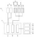
도1은 본원발명과 관련된 실시예1의 검사장치(10)의 구성을 모식적으로 나타내는 설명도이고,
도2는 검사장치(10)의 기능구성을 나타내는 블록도이고,
도3은 검사장치(10)의 유지스테이지(34)를 모식적으로나타내는 사시도이고,
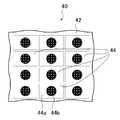
도4는 검사대상 워크(40)의 종류를 설명하기 위한 설명도로, (a)는 각 반도체 소자(44)가 테이프(42)에 붙여진 채로 각 경계면에서 절단된 상태를 나타내고, (b)는 테이프(42)가 잡아 늘여져 각 반도체소자(44)가 각각으로 분단된 상태를 나타내며,
도5는 검사장치(10)의 유지기구(13) 및 투명 조명기구(14)를 모식적으로 나타내는 사시도이고,
도6은 도5에서 나타내는 Ⅰ-Ⅰ선을 따르는 부위를 부분적인 단면으로 나타내는 설명도이고,
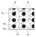
도7은 검사대상물로서의 일 예인 각 반도체 소자(44)를 나타내는 설명도이고,
도8은 도7에서 나타낸 각 반도체 소자(44)에서의 부적당한 예를 설명하기 위한 설명도이고,
도9는 관찰 광학계를 거쳐 관찰면(Fp) 위를 취득함으로써 얻은 촬상 카메라(24)에서의 화상 데이터에 있어서, 테이프(42)에서의 복수의 미세형상(M)으로 인한 그림자 부분이 발생되는 것을 설명하기 위한 설명도이고,
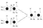
도10은 부적당한 각 반도체 소자(44)를 미세형상(M)에 기인하여 정상적인 두 개의 반도체 소자(44)로 판단해 버리는 모습을 설명하기 위한 설명도이고,
도11은 관찰 광학계를 거쳐 관찰면(Fp) 위를 취득함으로써 얻은 촬상 카메라(24)에서의 화상 데이터에 있어서, 테이프(42)에서의 복수의 미세형상(M)으로 인한 그림자 부분이 발생되는 것이 방지된 모습을 설명하기 위한 설명도이고,
도12는 실시예2의 검사장치(10A)의 구성을 모식적으로 나타내는 설명도이고,
도13은 실시예3의 검사장치(10B)의 유지기구(13B)의 구성을 모식적으로 나타내는 설명도이고,
도14는 실시예4의 검사장치(10C)의 지지기구(13C) 및 투과조명기구(14C)의 구성을 모식적으로 나타내는 설명도이다.1 is an explanatory diagram schematically showing the configuration of an
2 is a block diagram showing the functional configuration of the
3 is a perspective view schematically showing the
4 is an explanatory diagram for explaining the type of
5 is a perspective view schematically showing the
FIG. 6 is an explanatory view showing a portion along a line I-I shown in FIG. 5 in a partial cross section; FIG.
7 is an explanatory diagram showing each
FIG. 8 is an explanatory diagram for explaining an inappropriate example in each
Fig. 9 shows that in the image data of the
FIG. 10 is an explanatory view for explaining how each
Fig. 11 shows that in the image data of the
12 is an explanatory diagram schematically showing the configuration of an
Fig. 13 is an explanatory diagram schematically showing the configuration of the
14 is an explanatory diagram schematically showing the configuration of the
아래에 본 발명과 관련된 검사장치의 각 실시예에 관하여 도면을 참조하면서 설명한다.Hereinafter, each embodiment of the inspection apparatus related to the present invention will be described with reference to the drawings.
우선, 본원발명과 관련된 실시예1의 검사장치(10)의 개략적인 구성에 관하여 설명한다. 도1은 본원발명과 관련된 검사장치의 일례로서의 검사장치(10)의 구성을 모식적으로 나타내는 설명도이다. 도2는 검사장치(10)의 기능구성을 나타내는 블록도이다. 그리고, 도5에서는 이해를 쉽게 하기 위해 검사대상 워크(40)에서의 웨이퍼(41) 및 테이프(42)를 생략해서 나타내고 있다.First, a schematic configuration of an
검사장치(10)는 도1 및 도2에서 나타내는 바와 같이 관찰기구(11)와, 반사조명기구(12)와, 유지기구(13)와, 투과조명기구(14)와, 제어기구(15)로 대략적으로 구성되어 있다. 이 검사장치(10)는 도1에서와 같이 본체부(21)를 갖는다. 이 본체부(21)에는 도시는 생략되었지만, 릴레이렌즈나 리볼버 타입의 터릿부가 설치되어 있으며, 그 터릿부에는 복수의 대물렌즈 경통(22)이 설치되어 있다. 이 각 대물렌즈 경통(22)에는 대물렌즈(23)가 설치되어 있다. 이 본체부(21)의 상부에 촬상 카메라(24)가 고정되어 있다. 이 촬상카메라(24)는 설정된 대물렌즈(23)에 의해 정해지는 배율에 따라서 해당 대물렌즈(23) 및 본체부(21)(릴레이렌즈)를 거쳐 그 광축(관찰광축(Oa)) 상의 소정 위치의 화상 데이터를 취득할 수 있다. 이 때문에 촬상 카메라(24), 본체부(21), 각 대물렌즈 경통(22) 및 그 대물렌즈(23)는 관찰기구(11)에서의 관찰 광학계로서 기능하며, 그 광축이 관찰광축(Oa)이 된다. 또한, 관찰광축(Oa)상에서의 촬상 카메라(24)가 적절한 화상을 취득가능한 위치, 즉 관찰 광학계에서의 집점위치를 포함하여 해당 관찰광축(Oa)에 직교하는 평면(물체측의 결상면)이 관찰면(Fp)이 된다. 아래에서는 관찰광축(Oa)의 방향을 Z축 방향으로 하고, 거기에 직교하는 면을 X-Y평면으로 한다. 이 촬상 카메라(24)에 의해 취득된 화상 데이터는 후술하는 화상 제어부(61)에 의해 적절하게 해석되면서 모니터(39)에 표시가능하게 되어 있다(도2 참조).As shown in Figs. 1 and 2, the
그 본체부(21)의 내부에는 관찰광축(Oa) 상에 하프미러 또는 프리즘으로 구성된 반사부재(25)가 설치되어 있다. 본체부(21)에서는 반사부재(25)에 의한 관찰광축(Oa)으로부터의 반사방향으로 커넥터부(26)를 통하여 도광 화이버(27)가 설치되어 있다. 이 도광 화이버(27)는 동축용 광원(28)에서 출사된 조사광을 반사부재(25)로 도광하는 것이 가능하게 된다. 그 동축용 광원(28)은 도2에서와 같이 할로겐 램프(28a)와 스토로브(28b) 쌍방을 선택적으로 발광시키는 것이 가능하게 이루어져 있으며, 어느 것이 발광되어도 도광 화이버(27)로 출사시키는 것이 가능하게 이루어져 있다. 이 동축용 광원(28)에서 출사된 조명광은 도1에서와 같이 도광 화이버(27) 및 반사부재(25)를 거쳐 관찰광축(Oa) 위를 진행하고, 각 대물렌즈 경통(22)의 대물렌즈(23)를 거쳐 관찰광축(Oa) 상에서 관찰면(Fp)을 조명할 수 있다. 이 때문에 동축용 광원(28), 도광 화이버(27) 및 반사부재(25)는 각 대물렌즈 경통(22)의 대물렌즈(23)와의 협동에 의해, 관찰 광학계에 대하여 후술하는 검사대상물(44)에서의 동축방향에서의 반사광을 생성하기 위한 반사조명기구(12), 즉 동축낙사(落射)조명기구(29)로서 기능한다.Inside the
이 본체부(21)는 후술하는 Z축 구동기구(66)(도2참조)에 의해, 관찰광축(Oa)방향(Z방향)으로 이동할 수 있도록 되어 있다. 이 때문에 관찰기구(11)에서의 관찰 광학계와, 동축 낙사 조명기구(29)는 일체적으로 관찰광학(Oa)방향(Z방향)으로 이동할 수 있도록 되어 있다.The
또한, 본체부(21)에는 도1에서와 같이 대물렌즈 경통(22)의 외주를 포위하도록 하여서 조명광 도출용 링반(30)이 설치되어 있다. 이 조명광 도출용 링반(30)은 도시는 생략하지만 관찰광축(Oa)과 소정 간격을 두고 해당 관찰광축(Oa)을 에워싸도록 복수의 발광부가 설치되어 있으며, 각 발광부는 관찰광축(Oa)에 대하여 경사지는 방향에서 관찰면(Fp)을 향하여 조명할 수 있도록 되어 있다. 조명광 도출용 링반(30)에는 도광 화이버(31)가 설치되어 있다. 이 도광 화이버(31)는 링용 광원(32)에서 출사된 조사광을 조명광 도출용 링반(30)의 각 발광부(미도시)로 도광하는 것이 가능하게 이루어져 있다. 그 링용 광원(32)은 도2에서와 같이 할로겐램프(32a)와 스트로보(32b) 쌍방을 선택적으로 발광시키는 것이 가능하게 되어 있으며, 어느 쪽이 발광되어도 도광 화이버(31)로 출사시키는 것이 가능하게 이루어져 있다. 이 링용 광원(32)에서 출사된 조사광은 도1에서와 같이 도광 화이버(31)를 거쳐서 조명광 도출용 링 반(30)의 각 발광부(미도시)에서 관찰광축(Oa)에 대하여 경사진 방향으로 관찰면(Fp)을 조명할 수 있다. 이 때문에 링용 광원(32), 도광 화이버(31) 및 조명광 도출용 링반(30)(그 각 발광부)은 관찰 광학계에 대하여 후술하는 검사대상물(44)에서의 관찰광축(Oa)에 경사되는 방향에서의 반사광을 생성하기 위한 반사조명기구(12), 즉 사광(斜光) 조명기구(33)로서 기능을 한다. 이 조명도출용 링반(30)은 후술하는 Z축 구동기구(66)(도2참조)에 의해 관찰광축(Oa)(Z축방향)으로 이동가능하게 이루어져 있다. 이 관찰광축(Oa) 방향으로의 이동은 본체부(21)와 일체적인 것이어도 좋고, 서로 독립적인 것이어도 좋다.In addition, the
이 본체부(21) 및 조명광 도출용 링반(30)의 아래쪽에 유지기구(13)가 설치되어 있다. 이 유지기구(13)는 유지스테이지(34)를 갖는다. 이 유지스테이지(34)는 도3에서와 같이 단이 있는 원통형상을 나타내고 있으며 그 환상(고리모양)의 선단부(34a)에서 후술하는 검사대상물(44)의 유지부를 구성하고 있다. 이 선단부(34a)에서는 둥근 고리 모양의 환상홈(34b)이 설치되어 있으면서, 그 홈 안에 진공상태를 만들기 위한 흡인 홀(34c)이 마련되어 있다. 이 때문에 유지스테이지(34)에서는 후술되는 바와 같이 재치된 테이프(42)(도4참조)를 선단부(34a)에서 흡착 지지하는 것이 가능하게 되어 있다. 이 유지스테이지(34)에서는 그 내방에 투과(透過)스테이지(35)가 마련되어 있다.The holding
투과스테이지(35)는 도1, 도3, 도5 및 도6에서와 같이 원판형상을 띠며, 상측(관찰 광학계 측)의 상단면(35a)이 평탄면으로 이루어져 있으며, 하측(투과조명기구(14)의 후술하는 조사기구부(16) 측)의 하단면(35b)이 산란면으로 되어 있다. 이 상단면(35a)은 실시예1에서는 연마된 평탄면으로 되어 있으며, 하단면(35b)은 후술하는 바와 같은 산란 효과를 얻는 관점에서 확산율 등을 적절하게 고려해서 설정된다. 이 투과스테이지(35)는 적어도 투과조명기구(14)의 후술하는 조사기구부(16)(그 출사부(53))에서 출사된 투과광의 투과를 허락하는 투명한 부재(투과부재)로 형성되어 있으며, 실시예1에서는 유리로 형성되어 있다. 투과스테이지(35)는 그 주연부의 하단이 지지프레임(36)(도6참조)을 통하여 아래쪽에서 지지되어 있다.The
이 지지프레임(36)은 도6에서와 같이 둥근 고리모양을 띠며, 복수의 Z축 나사결합부재(37)(도6에서는 하나만 도시하고 있다)에 의해 하방에서 지지되고 있으면서 복수의 직교축 나사결합부재(38)(도6에서는 하나만 도시하고 있다)에 의해 Z축 방향 상측(관찰 광학계측)으로의 이동이 제한되어 있다. 각 Z축 나사결합부재(37)는 유지스테이지(34)를 Z축 방향으로 관통하여서 마련되어 있으며, 너트(37a)에 의해 Z축 방향에서의 위치결정이 가능하게 되어 있다. 이 Z축 나사결합부재(37)는 Z축을 중심으로 하는 회전방향에서 보아 소정 간격을 두도록 적어도 3점 이상 마련되어 있다. 각 직교축 나사결합부재(38)는 선단이 원추형상으로 이루어져 있으며, 지지프레임(36)의 상단위치의 경사면과의 계합(係合)이 가능하게 되어 있다. 이 때문에 유지스테이지(34)에서는 각 Z축 나사결합부재(37)에 의한 지지위치를 적절하게 변경함으로써 Z축 방향 즉 관찰광축(Oa) 방향에서 본 투과스테이지(35)의 위치(높이 위치)와, 해당 관찰광축(Oa)에 대한 투과스테이지(35)(상단면(35a)의 경사 쌍방을 조절 가능하게 해당 투과스테이지(35)가 마련되어 있다. 이로부터 각 Z축 나사결합부재(37)와 각 직교축 나사결합부재(38)는 유지스테이지(34)에 대하여 투과스테이지(35)를 관찰광축(Oa)에 관한 위치조정을 가능하게 유지하는 위치조정기구로서 기능을 한다.The
이 투과스테이지(35)는 두께 치수 즉 상단면(35a)과 하단면(35b)의 간격이 투과스테이지(35)에서의 광학적인 특성 및 경도 특성을 감안하면서 아래의 세 가지 면을 고려하여 설정되어 있다. 실시예1에서는 투과스테이지(35)의 두께 치수는 5cm~15cm의 범위로 전체적으로 균등한 것으로 이루어져 있다.The
첫째는, 투과조명기구(14)의 후술하는 조사기구부(16)에서 출사되어서 하단면(35b)으로 입사하여 상단면(35a)에서 출사한 투과광에 있어서 소정 광량을 확보할 수 있는 것이다. 이것은 투과스테이지(35)에서는 관찰 광학계를 거쳐서 촬상 카메라(24)로 취득한 화상을 보고, 후술하는 검사대상물(44)이 적절하게 조명되어 있을 필요가 있는 것에 따른다. 이점은 주로 투과스테이지(35)의 두께 치수의 상한값에 영향이 있다.First, it is possible to secure a predetermined amount of light in the transmitted light emitted from the
둘째는, 주연부의 하단이 아래쪽에서 지지되고 있는 것에 기인하여서, 중앙위치에서 처지는 듯한 휨 변형의 변형량이 소정 범위 이내라는 것이다. 이것은 투과스테이지(35)에서는 후술하는 바와 같이 상단면(35a)이 후술하는 검사대상물(44)을 관찰 광학계에서의 적절한 위치인 관찰면(Fp)상에 위치시키는 기능을 가지고 있어서 상단면(35a)을 전면에 걸쳐 관찰면(Fp)을 따르는 것으로 할 필요가 있는 것에 따른다. 이 때문에 상술한 변형량에서의 소정의 범위란, 최대로 관찰 광학계에서의 피사계 심도가 된다. 이 점은 주로 투과스테이지(35)의 두께 치수의 하한값에 영향을 미친다.Second, due to the lower end of the periphery being supported from below, the amount of deformation of the bending deformation that appears to sag at the central position is within a predetermined range. In the
셋째는, 산란면이 된 하단면(35b)에 의한 산란효과가 상단면(35a)에서 출사되는 투과광에 있어서 충분히 얻어지고 있는 것이다. 이것에 관해서는 나중에 상세하게 설명하기로 한다.Third, the scattering effect by the
이 투과스테이지(35)를 유지하는 유지스테이지(34)는 도1에서와 같이 후술하는 XY구동기구(64)(도2참조)에 의해 관찰광축(Oa)(관찰광학계)에 대하여 거기에 직교하는 X-Y평면상에서 이동가능하게 되어 있다. 또한, 유지스테이지(34)는 후술하는 회전구동기구(65)(도2참조)에 의해 Z축 둘레로 회전할 수 있도록 되어 있다. 이 유지스테이지(34)에는 검사대상워크(40)가 흡착 유지된다.The holding
검사대상워크(40)는 도4에서와 같이 웨이퍼(41)(유리기판 등도 포함하는 것으로 한다)가 붙여진 테이프(필름)(42)를 환상부재(43)의 안쪽에서 유지하여 구성되어 있다. 이 검사대상워크(40)에서는 (a)에 도시된 바와 같이 웨이퍼(41)로 형성된 복수의 반도체소자(44)가 테이프(42)에 붙여진 채 각 경계면에서 절단(다이싱)된 상태인 것과, (b)에 도시된 바와 같이 테이프(42)에 붙여져 절단된 뒤에 테이프(42)가 잡아 늘여져서 각개로 분단(익스팬드)된 상태인 것이 있다. 여기에서 환상부재(43)는 상태의 차이(검사대상 워크(40)의 종류)에 관계없이 유지스테이지(34)의 선단부(34a)(도1참조)보다 큰 지름 치수로 이루어져 있다. 검사장치(10)에서는 이들 중 어떤 상태라도 각 반도체소자(44)가 적절하게 형성되어 있는지 아닌지를 검사하기 위해 이용된다. 이 때문에 각 반도체 소자(44)를 검사대상물로서 검사대상 워크(40)의 상태를 유지한 채로 해당 검사대상물의 검사를 행할 수 있다.The
이 검사대상 워크(40)에서는 도1, 도5 및 도6에서와 같이 환상부재(43)의 안쪽에서 유지스테이지(34)가 위치되고 그 선단부(34a)에 테이프(42)가 재치된 상태에서 환상홈(34b) 및 흡인홀(34c)의 작용에 의해 테이프(42)가 선단부(34a)에 흡착 유지된다. 이때 유지스테이지(34)에 있어서, 투과스테이지(35)의 상단면(35a)이 선단부(34a)(흡착유지위치)보다도 위쪽(관찰광학계측)에 위치하는 것이 되면, 테이프(42)에서의 흡착 유지된 부분보다도 안쪽에 위치하는 영역이 투과 스테이지(35)의 상단면(35a)에 의해 잡아 당겨지므로 해당 상단면(35a)에 붙도록 평탄화된다(도1참조). 이 때문에 투과스테이지(35)를 관찰광축(Oa)에 관해서 위치 조정함으로써 테이프(42)에 붙여진 검사대상물(각 반도체 소자(44))을 적절한 상태로 관찰면(Fp) 위에 위치시킬 수 있다. 이 유지스테이지(34)의 아래쪽에 투과조명기구(14)로서의 조사(照射)기구부(16)가 설치된다(도1참조).In the
투과조명기구(14)는 도1에서와 같이 유지스테이지(34)에 의해 흡착 유지된 검사대상물(각 반도체소자(44))에 대하여 관찰 광학계(관찰기구(11))와는 반대측에서 투과광을 조사하는 것이다. 이 투과조명기구(14)는 조사기구부(16)를 갖는다. 그 조사기구부(16)는 후술하는 도광부(52)를 거쳐 투과용 광원(51)에서 출사된 투과광을 후술하는 출사부(53)로 도광하는 것이 가능하게 되어 있다. 그 투과용 광원(51)은 도2에서 나타내는 바와 같이 할로겐 램프(51a)와 스트로보(51b) 쌍방을 선택적으로 발광시킬 수 있게 되어 있으며, 어느 쪽이 발광되어도 도광부(52)로 출사시키는 것이 가능하게 되어 있다.The
이 조사기구부(16)는 상술한 투과용 광원(51)(도2참조)에 더하여 도5 및 도6에서와 같이 도광부(52)와 출사부(53)와 지지부(54)를 갖는다. 도광부(52)는 도시는 생략되지만, 일단측에 마련된 입사면이 투광용 광원(51)(도2참조)의 할로겐 램프(51a) 및 스트로보(51b)에서 발광된 빛(투과광)을 입사할 수 있도록 각각에 대향되어서 설치되어 있으며, 해당 입사면에서 입사된 투과용 광원(51)(도2참조)에서의 투과광을 타단측에 설치된 출사면(52a)(도6참조)로 인도한다. 이 도광부(52)는 실시예1에서는 광화이버로 형성되어 있다. 도광부(52)의 출사면(52a)에 출사부(53)가 접속되어 있다(도6참조).This
그 출사부(53)는 통 모양의 케이스체(53a)에 적어도 하나 이상의 광학소자(53b)가 수용되어서 구성된다. 이 광학소자(53b)는 도광부(52)의 출사면(52a)에 대향하는 입사면(53c)과, 거기서 입사된 투과광을 출사하는 출사면(53d)을 구성하고 있다. 광학소자(53b)는 입사면(53c)에서 입사된 투과광을 원하는 상태로 출사면(53d)에서 출사하도록 소정의 광학적 특성을 가지는 것으로 되어 있다. 이 광학소자(53b)의 중심축 위치가 되는 회전대칭축을 조사기구부(16)(투과조명기구(14)(투과조명계))의 투과광축(Pa)(도1참조)으로 한다. 이 조사기구부(16)에서는 도광부(52)에서 출사부(53)로 투과광이 입사되면, 출사부(53)에서 투과광축(Pa)을 따르는 투과광을 출사한다. 광학소자(53b)에서의 소정의 광학적 특징이란, 진행방향이 되는 투과광축(Pa)에 직교하는 단면에서 본 광량 분포가 균일해져 있는 것과, 조사영역의 퍼짐(확산)이 억제되어 있는 것을 말한다. 이 광학소자(53b)는 상술한 소정의 광학적 특성(인터그레이터 기능 및 확산 방지(집광)기능)을 갖는 광학소자로 구성되어 있으며, 실시예1에서는 광학소자(53b)는 로드 인터그레이터 광학부재로 구성되어 있다.The
또한, 실시예1에서는 케이스체(53a)에 있어서 광학소자(53b)의 입사면(53c)보다도 아래쪽에 위치하는 하단부(53e)가 통모양으로 이루어져 있으며, 도광부(52)의 타단부(출사면(52a)이 마련되어 있는 쪽의 단부)를 안쪽에서 삽입 가능하도록 이루어져 있다. 이 때문에 출사부(53)와 도광부(52)는 도광부(52)의 타단부를 출사부(53)의 하단부(53e)에 끼워넣음으로써 도광부(52)의 출사면(52a)과 출사부(53)의 입사면(53c)이 맞닿아져 연결(접속)된다. 이러한 상태에서 도광부(52)와 출사부(53)가 지지부(54)에 의해 고정적으로 지지되어 있다.In addition, in Example 1, the
이 때문에 조사기구부(16)에서는 투과용 광원(51)에서 출사한 투과광을 도광부(52)를 거쳐 출사부(53)로 진행시켜 균일한 광량 분포의 대략 평행광으로서 출사부(53)에서 투과광축(Pa)(도1참조) 방향을 향해 출사시켜서 투과스테이지(35)의 하단면(53b)을 조사할 수 있다. 이 투과광은 산란면이 된 하단면(35b)에 의해 산란광이 되어서 관찰면(Fp)을 이면 쪽에서 조사한다. 이 투과광은 적어도 유지스테이지(34)에 흡착 유지된 검사대상워크(40)의 테이프(42)를 투과하여 관찰 광학계(촬상카메라(24))에 의해 관찰가능하게 이루어져 있다(도1참조). 이 때문에 조사기구부(16)(투과용 광원(51), 도광부(52) 및 출사부(53))는 산란면이 된 투과스테이지(35)의 하단면(35b)과 협력하여서 관찰 광학계와는 반대측에서 관찰면(Fp)(검사대상물(반도체소자(44))를 조사하는 투과광을 생성하는 투과조명기구(14)로서 기능을 한다. 실시예1에서는 투과광축(Pa)이 Z축 방향으로 평행하게 설정되어 있으며, 투과광축(Pa)과 관찰광축(Oa)이 일치하도록 관찰 광학계에 대한 조사기구부(16)의 위치가 설정되어 있다. 또한, 투과조명기구(14)는 로드 인터그레이터 광학부재로 구성된 조사기구부(16)의 광학소자(53b)에 의해 관찰면(Fb) 상에서 본 투과광의 조사영역에서 관찰 광학계(촬상카메라(24))에 의해 관찰가능한 관찰영역을 충족하는 것을 가능하도록 설정되어 있다.For this reason, the
이 검사장치(10)에서는 상술한 바와 같이 구성된 관찰기구(11), 반사조명기구(12), 유지기구(13) 및 투과조명기구(14)가 제어기구(15)(도2참조)의 제어하에서 총괄적으로 제어된다. 이 제어기구(15)는 도2에서와 같이 화상제어부(61)와 조명제어부(62)와 구동제어부(63)를 가지고 있다.In this
화상제어부(61)는 촬상카메라(24)에 의해 취득된 화상 데이터를 적절하게 해석한다. 이 해석이란, 테이프(42)에 붙여진 복수의 검사대상물(반도체소자(44))의 윤곽선을 인식하는 것이나, 관찰점에서의 포커스 상태를 판단하는 것이나, 각 검사대상물에서의 결함을 인식하는 것이나, 각 검사대상물에 마련된 전극이나 배선 등의 불비를 인식하는 것이나, 웨이퍼(41)에서의 각 검사대상물(반도체소자(44))의 절단불량을 인식하는 것 등을 들 수 있다. 또한, 화상제어부(61)는 촬상 카메라(24)에 의해 취득된 화상 데이터를 근거로 하는 영상을 모니터(39)에 표시시킨다.The
조명제어부(62)는 동축용 광원(28)과 링용 광원(32)과 투과용 광원(51)을 적절하게 점등 소등 제어를 한다. 즉, 조명제어부(62)는 동축용 광원(28), 링용 광원(32) 및 투과용 광원(51)에 있어서, 할로겐 램프(28a,32a,51a) 혹은 스트로브(28b,32b,51b)를 선택적으로 적절하게 점등 소등시키면서 동축용 광원(28), 링용 광원(32) 및 투과용 광원(51)을 동시에 또는 개별로 점등 및 소등시킨다. 이 할로겐 램프(28a,32a,51a)는 관찰용 조명으로서 이용하는 것이며, 스트로보(28b,32b,51b)는 검사용 조명으로 이용하는 것이다. 또한, 조명제어부(62)는 각 광원(28,32,51)에 있어서 검사용 조명으로서의 스트로브(28b,32b,51b)의 밝기 조정이 가능하게 되어 있다. 이 밝기 조정은 예를 들면, 복수의 ND 필터 중 어느 것을 적절하게 선택함으로써 실현할 수 있다.The
구동제어부(63)는 XY구동기구(64), 회전구동기구(65) 및 Z축 구동기구(66)를 적절하게 구동 제어한다. 즉, 구동제어부(63)는 Z축 구동기구(66)를 구동제어함으로써 관찰기구(11)에서의 관찰 광학계 및 동축 낙사 조명기구(29)를 관찰광축(Oa)방향(Z축 방향)으로 적절하게 이동시킬 수 있으면서, 사광(斜光)조명기구(33)를 관찰광축(Oa)방향(Z축 방향)으로 적절하게 이동시킬 수 있다. 이에 의해 유지스테이지(34)에 흡착 유지된 검사대상 워크(40)의 검사대상물(각 반도체소자(44))를 적절한 조명하에서 적절하게 관찰하는 것을 가능하게 한다. 또한, 구동제어부(63)는 XY구동기구(64) 및 회전구동기구(65)를 구동제어함으로써 유지스테이지(34) 즉 그곳에 흡착 유지된 검사대상워크(40)를 관찰광축(Oa)(관찰광학계) 및 투과광축(Pa)(조사기구부(16))에 대하여 거기에 직교하는 X-Y 평면상에서 적절하게 이동시킬 수 있으면서 관찰광축(Oa)(투과광축Pa(Z축 방향)) 둘레로 적절하게 회전시킬 수 있다. 이에 의해 유지스테이지(34)에 흡착 유지된 검사대상워크(40)에서의 임의 위치의 검사대상물(반도체소자(44))을 검사하는 것이 가능해진다.The
제어기구(15)에서는 이 밖에도 상술한 유지스테이지(34)에서의 흡착 동작의 제어 등이 가능하게 이루어져 있으면서 검사를 위한 화상 데이터의 비교 등이 가능하게 되어 있다.In addition to the
이 검사장치(10)에서는 우선 검사 대상으로 하는 검사대상물이 첨부된 검사대상워크(40)를 따라서 투과스테이지(35)의 관찰광축(Oa)에 관한 위치조정을 행한다. 이것은 아래에 의한다. 검사장치(10)에서는 유지스테이지(34)의 선단부(34a)에서 환상부재(43)의 내방위치의 테이프(42)를 흡착 유지하는 것이어서 테이프(42)의 주연부가 하방에서 지지되어 있는 것에 기인하여 중앙위치가 처지듯이 휨 변형하는 경우가 있다. 그러면, 이 휨 변형에 의해 테이프(42) 상의 각 반도체소자(44)가 관찰면(Fp)으로부터 벗어나게 되어 관찰 광학계(촬상카메라(24))에 의한 적절한 관찰을 할 수 없게 될 우려가 있다. 이 테이프(42)의 휨 변형량 및 상태는 테이프(42)의 재질이나 첨부된 각 반도체소자(44)의 위치 및 개수 등에 따라서 달라지는 것이어서 검사대상 워크(40)의 종류에 따라서 달라지는 것이 된다. 이 때문에 대상이 되는 검사대상 워크(40)를 유지스테이지(34)에서 흡착 유지한 상태에 있어서, 테이프(42) 상의 각 반도체 소자(44)를 관찰면(Fp) 위에 위치시키도록 테이프(42)의 휨 변형량 및 상태에 따라서 투과스테이지(35)의 Z축 즉 관찰광축(Oa) 방향에서 본 위치(높이 위치)와, 해당 관찰광축(Oa)에 대한 투과스테이지(35)(상단면(35a))의 경사 쌍방을 조절한다.In this
이때, 테이프(42)의 휨 변형이 클수록 투과스테이지(35)의 상단면(35a)을 유지스테이지(34)의 선단부(34a)(흡착 유지 위치)보다도 상방(관찰광학계측)에 위치시킨다. 이것은 이하의 것에 의한다. 투과스테이지(35)의 상단면(35a)을 유지스테이지(34)의 선단부(34a)보다도 위쪽에 위치시키면, 테이프(42)에서의 흡착 유지된 개소보다도 안쪽에 위치하는 영역이 투과스테이지(35)의 상단면(35a)에 의해 상방으로 잡아당겨지기 때문에 해당 상단면(35a)에 테이프(42)가 붙도록 평탄화된다. 이 때문에 테이프(42)의 휨 변형에 따라서, 투과스테이지(35)의 상단면(35a)을 상방에 위치시킴에 따라 테이프(42)에 붙여진 검사대상물(각 반도체 소자(44))을 보다 적절한 상태로 관찰면(Fp) 상에 위치시킬 수 있다. 이때, 투과스테이지(35)의 상단면(35a)에 높이 위치를 따라서 관찰기구(11), 반사조명기구(12) 및 투과조명기구(14)의 조명기구부(16)를 Z축 방향으로 적절하게 이동시키는 것은 말할 필요도 없다. 이 테이프(42)의 휨 변형량 및 상태는, 예를 들면 촬상카메라(24)에서의 화상 데이터를 화상제어부(61)에서 해석함으로써 취득할 수 있다.At this time, the larger the deflection deformation of the
검사장치(10)에서는 이어서 유지스테이지(34)에서 검사대상워크(40)를 흡착유지하고, 칩 스캔을 행한다. 이 칩 스캔에서는 유지스테이지(34)의 선단부(34a)의 내방위치, 즉 검사대상 워크(40)(테이프(42))에 있어서 흡착 유지된 개소보다도 안쪽 위치를 전면에 걸쳐서 주사하도록 구동제어부(63)에 의해 관찰광축(Oa)에 대하여 유지스테이지(34)를 이동시킨다. 이 주사에서는 투명조명기구(14)에서의 투과광을 조사하면서 촬상카메라(24)에 의한 화상 취득을 행한다.In the
이어서, 칩맵을 작성한다. 이 칩맵이란, 검사대상워크(40)(테이프(42))에서의 각 검사대상물(반도체소자(44))의 위치, 및 자세를 나타내는 것이다. 제어기구(15)에서는 칩 스캔에 의한 윤곽선을 인식함으로써 테이프(42)에 붙여진 복수의 검사대상물(반도체소자(44))를 판별하면서 구동제어부(63)에 따른 이동위치정보를 가미함으로써 각 검사대상물(반도체소자(44))의 위치 및 자세를 취득한다.Next, a chip map is created. This chip map shows the position and attitude | position of each test object (semiconductor element 44) in the test | inspection workpiece | work 40 (tape 42). The
이어서 검사대상물(반도체소자(44))의 판정을 한다. 이 판정에서는 작성한 칩맵을 근거로 관찰 광학계에 의한 관찰위치를 결정하고, 그 결정에 따라서 구동제어부(63)에 의해 유지스테이지(34)를 이동시킨다. 그 후, 그 관찰위치에 있는 검사대상물(반도체소자(44))을 그 검사대상물의 양품 데이터와 비교하여 해당 검사대상물(반도체소자(44))의 좋고 나쁨을 판단하다. 이 양부 판단은 촬상 카메라(24)에서의 화상 데이터를 화상 제어부(61)에서 해석함으로써 수행한다.Next, the inspection object (semiconductor element 44) is determined. In this determination, the observation position by an observation optical system is determined based on the created chip map, and the holding
이 검사대상물(반도체소자(44))의 판정을 작성한 칩맵을 근거로 검사대상워크(40)(테이프(42)) 상의 모든 검사대상물(반도체소자44))에 대하여 순차적으로 행함으로써 해당 검사대상워크(40)에 대한 검사가 종료한다. 그리고, 이 검사는 화상제어부(61)의 제어하에서 모니터(38)에 표시된 촬상카메라(24)에 의해 취득된 화상데이터에 의거하는 영상을 눈으로 보아 수행할 수도 있다.Based on the chip map on which the determination of the inspection object (semiconductor element 44) is made, all inspection objects (semiconductor element 44) on the inspection target work 40 (tape 42) are sequentially performed to perform the inspection object work. The check on 40 ends. This inspection can also be performed by visually viewing an image based on the image data acquired by the
(기술의 과제)(Technical Challenges)
이어서 종래의 검사장치에서의 기술 과제에 관하여, 도7 내지 도10을 이용하여서 설명한다. 그리고, 이 기술 과제에 관해서는 투과스테이지(35)의 하단면(35b)이 산란면으로 되어 있지 않은 것으로 한다면, 본원발명과 관련된 검사장치(10)에서도 같은 문제가 발생하기 때문에 아래의 설명에서는 이해를 돕기 위하여 검사장치(10)를 이용하여 설명한다. 또한, 도7 내지 도10에서는 이해를 돕기 위해 각 반도체 소자(44)의 상태나 후술하는 미세형상(M)(도9 참조)을 강조하여서 나타내고 있는데, 실제의 검사대상물이나 관찰상태와 반드시 일치하는 것은 아니다.Next, the technical problem in the conventional inspection apparatus is demonstrated using FIGS. In this technical problem, if the
검사장치(10)에서는 상술한 바와 같이 유지스테이지(34)에서 검사대상 워크(40)를 흡착유지하면, 우선 칩 스캔을 하여서 촬상 카메라(24)에서의 화상데이터의 해석에 의해 칩맵을 작성한다. 이때, 검사장치(10)에서는 촬상 카메라(24)로부터의 화상데이터에 있어서, 각 반도체소자(44)의 윤곽선을 인식할 필요가 있다. 이러한 인식을 위해 검사장치(10)에서는 투과조명기구(14)(그 조사기구부(16))에서 투과광을 조사하면서 촬상카메라(24)에 의한 화상 데이터의 취득을 수행한다.As described above, when the
도7에서와 같이 검사대상 워크(40)의 테이프(42) 상에 있어서, 직사각형상의 각 반도체소자(44)가 정렬해 있는 것을 검사대상물로 하기로 한다. 이 예(도7 내지 도11)의 각 반도체소자(44)는 직사각형상으로 투명한 유리기판(44a)의 중앙에 도전체로 이루어지는 전극(44b)이 설치된 LED칩을 모식적으로 나타낸 것이며, 도시는 생략하지만, 유리기판(44a)상에도 여러 배선이 설치되어 있다. 이 때문에 이 검사대상워크(40)에서는 각 반도체소자(44)의 유리기판(44a) 및 테이프(42)가 투과광의 투과를 허락하는 것이며, 촬상 카메라(24)에서 취득된 화상데이터에 있어서, 각 반도체소자(44)의 유리기판(44a) 및 테이프(42)가 밝은 것이 된다.As shown in FIG. 7, it is assumed that the
여기에서 상술한 화상해석으로는 투과조명기구(14)(그 조사기구부(16))에서의 투과광이 조사된 각 반도체소자(44)의 윤곽선을 인식할 필요가 있지만, 각 반도체 소자(44)가 투과광의 투과를 허락하지 않는 것인 경우, 그 윤곽선은 명확한 것이어서 문제가 되는 일은 없다. 그렇지만, 이 예의 투명한 유리기판(44a)으로 구성된 각 반도체소자(44)와 같이 외형형상을 구성하는 부재가 투과광의 투과를 허락하는 재료로 형성된 것을 검사대상물로 하는 경우, 테이프(42)와 유리기판(44a)이 밝게 표시되어서 윤곽선만이 엷은 그림자가 되는 것이어서 미세한 명암(콘트라스트)을 근거로 윤곽선을 인식할 필요가 있다.In the above-described image analysis, it is necessary to recognize the contour of each
이 검사대상 워크(40)에서는 웨이퍼(41)(도4참조)에서의 분석에 의해 각 반도체소자(44)가 형성되는 것이어서, 테이프(42) 상에서는 도8에서와 같이 서로 이웃하는 두 개의 반도체 소자(44)의 분단선이 부적절한 것이 되거나(왼쪽 위를 참조), 서로 이웃하는 두 개의 반도체 소자(44)가 분단되어 있지 않거나(오른쪽 아래를 참조) 하는 경우가 있다. 이와 같은 반도체소자(44)(검사대상물)가 있는 경우, 이러한 상태인 것, 즉 도8에서의 왼쪽 위의 두 개의 반도체 소자(44) 및 오른쪽 아래의 두 개의 반도체 소자(44)가 불량품이라는 것을 적확하게 검출할 필요가 있다.In the
그러나, 이 예의 각 반도체 소자(44)는 투명한 유리기판(44a)으로 구성되어 있으면서 투과광의 투과를 허락하는 테이프(42)에 붙여져 있다. 여기에서 테이프(42)에서는 투과조명이 조사된 상태를 관찰 광학계(촬상카메라24)에서의 화상 데이터로 관찰하면, 어떤 부재가 붙여져 있지 않은 상태에서도 한결같이 밝은 상태가 아니라 선모양이나 점모양의 부분적으로 어두운 곳(도9의 부호M 참조)이 존재하게 된다. 이하에서는 이 부분적으로 어두운 곳을 테이프(42)에서의 미세형상(M)이라 한다. 이 미세형상(M)은 테이프(42)에 먼지 등이 부착해 있거나 접착제의 얼룩이 발생되거나 하는 것이 기인한 것으로 생각될 수 있다.However, each
이로 인해 이러한 예의 투명한 유리기판(44a)으로 구성된 각 반도체소자(44)와 같이 외형형상을 구성하는 부재가 투과광의 투과를 허락하는 재료로 형성된 것을 검사 대상물로 하면, 촬상 카메라(24)에서의 화상데이터에서는 도9에서와 같이 각 전극(44b)에 의한 그림자 부분 사이에 각 유리기판(44a)의 윤곽선에 의한 그림자 부분과 복수의 미세형상(M)에 의한 그림자 부분이 혼재하게 된다.Therefore, when the inspection object is formed of a material that allows transmission of transmitted light, such as each
이 때문에 도10에서와 같이 서로 이웃하는 두 개의 반도체 소자(44)의 분단선이 부적절한 것(왼쪽 위를 참조)이나, 서로 이웃하는 두 개의 반도체 소자(44)가 분단되어 있지 않은 것(왼쪽 아래 참조)이라 해도, 그 사이에 존재하는 미세형상(M)을 양 반도체소자(44)의 윤곽선(분단선)으로 판단해 버릴 우려가 있다. 이때문에 부적절한 분단선이 된 두 개의 반도체 소자(44)나, 연속된 두 개의 반도체 소자(44)를 정상적인 두 개의 반도체 소자(44)가 서로 이웃하여 있는 것(우측 참조)으로 판단해 버려 이들 불량품을 적확하게 검출할 수 없어질 우려가 있다. 즉, 화상 데이터 상에서, 테이프(42)의 각 미세형상(M)이 노이즈 성분으로 작용하게 되어, 해당 검사대상물(44)의 검사 정밀도가 저하될 우려가 있다. 이 때문에 어떤 대책에 의해 해당 노이즈 성분을 제거하는 것이 바람직하다.For this reason, as shown in FIG. 10, the dividing line of two neighboring
(산란면에 의한 작용)(Action by scattering surface)
검사장치(10)에서는 관찰 광학계를 거쳐서 관찰면(Fp) 상을 취득함으로써 얻은 촬상 카메라(24)에서의 화상 데이터의 테이프(42)의 미세형상(M)을 제거하기 위하여 투과 스테이지(35)의 하단면(35b)이 산란면으로 이루어져 있다. 이 때문에 투과조명기구(14)의 조사기구부(16)에서 출사된 투과광은 산란면이 된 하단면(35b)에서 투과 스테이지(35) 내로 입사하여서 상단면(35a)에서 출사하여 테이프(42)에 붙여진 각 반도체소자(44)를 이면 쪽에서 조사한다. 이로부터 해당 투과광은 하단면(35b)에 의해 산란되고, 테이프(42) 및 거기에 붙여진 각 반도체 소자(44)로 도달하게 된다. 이와 같이 테이프(42)를 조사하는 투과광이 소정의 산란 상태가 되어 있으면, 관찰 광학계를 거쳐 촬상 카메라(24)로 취득한 화상 데이터에 있어서, 테이프(42)의 미세형상(M)을 거의 인식할 수 없게 할 수 있다. 이것은 테이프(42)의 미세형상(M)에 대하여 여러 각도 방향에서 투과광이 조사하는 것에 기인하는 것으로 생각될 수 있다.In the
이 때문에 투과스테이지(35)에서는 상술한 바와 같이 두께 치수 즉 상단면(35a)과 하단면(35b)의 간격이 산란면이 된 하단면(35b)에 의한 산란효과를 고려하여서 결정된다. 즉, 관찰면(Fp)상의 테이프(42)를 조사하는 투과광(상단면(35a)에서 출사된 투과광)을 소정의 산란상태로 하는 것을 가능하게 하도록 투과스테이지(35)의 두께 치수가 하단면(35b)에서의 산란면의 정도(粗面度)를 감안하여서 설정되어 있다. 여기에서 소정의 산란상태란, 촬상 카메라(24)로부터의 화상 데이터에서의 테이프(42)의 미세형상(M)을 제거하는 것, 즉 투과조명기구(14)에서의 투과광이 조사된 관찰면(Fp)상의 테이프(42)를 관찰 광학계를 거쳐 촬상카메라(24)로 취득했을 때, 그 화상 데이터에 있어서 테이프(42)가 한결같이 밝은 상태가 되는 것을 말한다.For this reason, in the
이와 같이 구성된 검사장치(10)에서는 상술한 투명한 유리기판(44a)으로 구성된 각 반도체소자(44)(도7참조)를 투과조명을 조사하면서 관찰 광학계(촬상카메라(24)에서의 화상 데이터로 관찰하면, 도11에서와 같이 테이프(42)에서의 복수의 미세형상(M)에 의한 그림자 부분이 생기는 것을 방지할 수 있어서 화상 데이터 상에서의 노이즈 성분을 제거할 수 있다. 이 때문에 각 반도체소자(44)의 윤곽선 판단을 정확한 것으로 할 수 있다. 예를 들면 도10에서와 같이 서로 이웃하는 두 개의 반도체 소자(44)의 분단선이 부적절한 것(왼쪽 위 참조)은 그 부적절한 상태에서 서로 이웃하는 두 개의 반도체 소자(44)가 분단되어 있지 않은 것(왼쪽 아래를 참조)은 그 연속한 상태에서 인식할 수 있기 때문에 그러한 불량품을 적확하게 검출할 수 있다.In the
이와 같이 본 발명과 관련된 검사장치(10)로는 투과 스테이지(35)의 산란면이 된 하단면(35b)에 의한 산란효과에 의해 관찰 광학계(촬상 카메라24)에서의 화상 데이터에 있어서 투과조명기구(14)에서의 투과광이 조사된 테이프(42)에서의 복수의 미세형상(M)에 의한 그림자 부분이 발생되는 것을 방지할 수 있어서, 투과조명기구(14)를 이용하여 테이프(42)에 첨부된 검사대상물(실시예1에서는 각 반도체소자(44))의 정보를 정확하게 얻을 수 있다.As described above, the
또한, 검사장치(10)에서는 산란면이 된 하단면(35b)이 투과광축Pa방향에서 보아 관찰면(Fb)을 따른 평면을 규정하는 투과 스테이지(35)의 상단면(35a)에서 소정의 간격을 두고 설치되어 있어서 산란면이 된 것에 의한 산란효과를 확실하게 얻 수 있기 때문에 관찰 광학계(촬상카메라(24))에서의 화상데이터에 있어서 투과조명기구(14)에서의 투과광이 조사된 테이프(42)에서의 복수의 미세형상(M)에 의한 그림자 부분이 생기는 것을 확실하게 방지할 수 있다.In addition, in the
그리고 또한 검사장치(10)에서는 투과광축(Pa) 방향에서 본 상단면(35a)과 산란면(하단면(35b))의 간격이 투과조명기구(14)에서의 투과광(조사기구부(16)에서 출사되어서 산란면을 거친 투과광)이 조사된 관찰면(Fp)상의 테이프(42)를 관찰 광학계를 거쳐 촬상 카메라(24)로 취득했을 때 그 화상데이터에 있어서 테이프(42)가 한결같이 밝은 상태가 되는 것을 기준으로 해서 하단면(35b)에서의 산란면 정도(조면도)에 맞춰서 설정되어 있어서 산란면이 된 것으로 인한 산란효과를 보다 확실하게 얻을 수 있다. 그리고 유리로 형성된 투과스테이지(35)의 상단면(35a)을 관찰면(Fp)으로 하며 또한 하단면(35b)을 산란면으로 하여 실험했더니, 관찰면(Fp)과 산란면의 간격을 3㎝이상으로 함으로써 원하는 산란효과를 얻을 수 있었다.In addition, in the
검사장치(10)에서는 투과스테이지(35)의 상단면(35a)이 검사대상물(실시예1에서는 각 반도체 소자(44))을 관찰면(Fp)상에 위치시키면서 평탄한 상태로 하는 기능을 가지고 있어서, 해당 검사대상물을 관찰 광학계(관찰기구(11))에 의해 적절하게 관찰할 수 있다.In the
검사장치(10)에서는 검사대상물을 관찰면(Fp) 상에 위치시키는 상단면(35a)이 설치된 투과스테이지(35)의 하단면(35b)에서 투과조명기구(14)로서의 산란면을 구성하고 있어서, 관찰 광학계(관찰기구(11))에 있어서 적절한 관찰지점인 관찰면(Fp)(상단면(35a))에 대한 투과광축(Pa)방향에서 본 산란면(하단면(35b))의 위치, 즉 투과광축(Pa) 방향에서 본 관찰면(Fp)과 산란면의 간격을 용이하며 확실하게 설정할 수 있다.The
검사장치(10)에서는 상단면(35a)이 설치된 투과스테이지(35)의 하단면(35b)에서 투과조명기구(14)로서의 산란면을 구성하고 있어서 검사대상물을 관찰면(Fp) 상에 위치시키는 기능 및 화상 데이터 상에서의 노이즈 성분을 제거하는 기능을 투과스테이지(35)를 설치하는 것만으로 실현할 수 있어서 쉽게 구성할 수 있다.In the
검사장치(10)에서는 투과광축(Pa) 방향에서 본 상단면(35a)과 하단면(35b)의 간격(투과스테이지(35)의 두께 치수)이 조사기구부(16)에서 출사되어서 투과스테이지(35)를 거친 투과광에서의 광량도 고려하여 설정되어 있어서, 소정의 광량으로 관찰면(Fp) 상의 검사대상물에 투과광을 조사할 수 있기 때문에 투과조명기구(14)를 이용하여서 검사대상물(실시예1에서는 각 반도체 소자(44))의 정보를 보다 정확하게 얻을 수 있다.In the
검사장치(10)에서는 투과광축(Pa) 방향에서 본 상단면(35a)과 하단면(35b) 간격(투과 스테이지(35)의 두께 치수)이 투과스테이지(35)의 휨 변형의 변형량을 소정의 범위 이내로 하는 점도 설정되어 있어서 관찰 광학계(촬상카메라(24))에 의해 적절하게 관찰할 수 있다.In the
검사장치(10)에서는 검사대상 워크(40)(그 테이프(42))를 유지스테이지(34)에서 흡착 유지할 때, 투과스테이지(35)의 상단면(35a)을 유지스테이지(34)의 선단면(34a)(흡착유지위치)보다도 위쪽(관찰광학계)에 위치하는 것으로 할 수 있어서 테이프(42)에 첨부된 검사대상물(각 반도체소자(44))을 보다 적절하게 관찰면(Fp) 상에 위치시킬 수 있다.In the
검사장치(10)에서는 투과스테이지(35)가 위치조정기구에 의해 유지스테이지(34)에 대하여 관찰광축(Oa)에 관한 위치조정이 가능하게 되어 있어서, 테이프(42)의 휨 변형량 및 상태에 따라서 테이프(42)에 붙여진 검사대상물(각 반도체소자(44))를 보다 적절하게 관찰면(Fp)상에 위치시킬 수 있다.In the
검사장치(1O)에서는 투과조명기구(14)의 조사기구부(16)(그 출사부(53)가 조사영역의 퍼짐(확산)을 억제하는 광학성능(인터그레이터 기능)을 가지고 있어서, 관찰면(Fp)상에서의 관찰 광학계(촬상카메라(24))에 대한 적절한 영역을 조사할 수 있기 때문에 보다 효율적으로 관찰 광학계(촬상카메라(24))에 의한 적절한 관찰을 가능하게 할 수 있다.In the
검사장치(10)에서는 투과조명기구(14)의 조사기구부(16)(그 출사부(53))가 진행방향이 되는 투과광축(Pa)에 직교하는 단면에서 본 광량 분포를 균일화하는 광학성능(확산방지(집광)기능)을 가지고 있기 때문에 관찰 광학계(촬상카메라(24))에 의한 보다 적절한 관찰을 가능하게 할 수 있다.In the
검사장치(10)에서는 투과조명기구(14)의 조사기구부(16)(그 출사부(53))가 유지스테이지(34)에서 떨어진 위치에서 해당 유지스테이지(34)에 흡착 유지된 검사대상물(실시예1에서는 각 반도체소자(44))을 조사하는 구성이기 때문에 유지스테이지(34)의 X-Y 평면을 따르는 이동에 따라 해당 유지스테이지(34)와 조사기구부(16)(그 출사부(53))가 간섭하는 것을 확실하게 방지할 수 있어서 유지스테이지(34)에 있어서 테이프(42)를 흡착 유지하는 선단부(34a)의 안쪽의 전 영역에 투과광을 조사할 수 있기 때문에 유효한 검사영역을 최대한으로 확보할 수 있다. 이것은 조사기구부(16)(그 출사부(53))가 Z축 방향에서 보아 유지스테이지(34)와 겹치도록 해당 유지스테이지(34)의 안쪽에 위치되어 있는 경우, 출사부(53)의 케이스체(53a)와 유지스테이지(34)의 내주벽면의 간섭에 의해 유지스테이지(34)의 내방에서의 투과광을 조사가능한 영역(유효한 검사영역)이 좁아져 버리게 된다. 이 때문에 유지스테이지(34)에 흡착 유지된 테이프(42)에 첨부된 검사 대상물을 투과조사기구(14)를 이용해서 효율적으로 적절히 검사할 수 있다.In the
따라서, 본 발명과 관련된 검사장치(10)에서는 테이프(42)에 붙여진 투명한 검사 대상물(각 반도체 소자(44))에 대해서도 투과조명에 의해 정확한 정보를 얻을 수 있다.
Therefore, in the
이어서, 본 발명의 실시예2와 관련된 검사장치(10A)에 관하여 도12를 이용하여 설명한다. 이 실시예2는 실시예1의 검사대상(10)에 대하여 유지스테이지(34A)(유지기구(13A))에서의 위치조정기구의 구성이 다른 예이다. 이 실시예2의 검사장치(10A)는 기본적인 구성은 상기한 실시예(1)의 검사장치(10)와 같기 때문에 동등한 구성 개소에는 같은 부호를 붙이고, 그 상세한 설명은 생략한다.Next, an
검사장치(10A)에서는 도12에서와 같이 유지기구(13A)의 유지스테이지(34A)에서의 위치조정기구로서 각 Z축 나사결합부재(37) 대신에 복수의 Z축 조정기구(71)가 설치되어 있다. 이 Z축 조정기구(71)는 Z축 나사결합부재(37)와 마찬가지로 적어도 3점 이상 설치되어 있다(도12에서는 2개만 도시한다). 각 Z축 조정기구(71)는 구동모터(72)와, 그 회전축(72a)에 설치된 캠부재(73)와, 그에 의해 변동되는 Z축 지지부(74)를 갖는다. 구동모터(72)는 Z축 조정기구(71)에서의 구동원이며, 회전축(72a)에서 회전구동력을 출력한다. 그 회전축(72a)에 캠부재(73)가 접속되어 있다. 그 캠부재(73)는 원판형상을 띠며 축선에서 편심된 위치에서 회전축(72a)에 접속되어 있다. 캠부재(73)은 외측면에서 Z축 지지부(74)에 맞닿을 수 있게 되어 있다. 그 Z축 지지부(74)는 막대기 형상을 띠며 Z축 방향에서 보아 캠부재(73)의 상측(투과스테이지(35)측)에서 유지스테이지(34A)를 Z축 방향으로 관통하여 설치되어 있으며, Z축 방향에 이동 자유롭게 되어 있다. Z축 지지부(74)는 상측(관찰광학계 측)의 일단이 지지프레임(36)을 하방에서 지지하고 있으며, 하측의 타단이 캠부재(73)의 외측면에 맞닿아져 있다.In the
이 Z축 조정기구(71)에서는 구동모터(72)를 적절하게 구동제어함으로써 캠부재(73)의 회전축(72a) 회전의 회전 자세에 따라서 Z축 지지부(74)를 Z축방향으로 이동시킬 수 있다. 이 때문에 유지스테이지(34A)에서는 각 Z축 조정기구(71)를 적절하게 구동시켜서 각 Z축 지지부(74)에 의한 지지위치를 적절하게 변경함으로써 Z축 방향 즉 관찰광축(Oa) 방향에서 본 투과스테이지(35)의 위치(높이 위치)와, 해당 관찰광축(Oa)에 대한 투과스테이지(35)(상단면(35a))의 경사, 쌍방을 조정할 수 있게 해당 투과스테이지(35)가 설치되어 있다. 이로부터 각 Z축 나사결합부재(37)는 유지스테이지(34A)에 대해서 투과스테이지(35)를 관찰광축(Oa)에 관한 위치조정을 가능하게 유지하는 위치조정기구로서 기능한다. 검사장치(10A)에서는 제어기구(15)의 구동제어부(63)가 각 Z축 조정기구(71) 즉 그 구동모터(72)를 적절하게 구동제어하는 것이 가능하게 되어 있다.In the Z-
이 검사장치(1OA)에서는 대상이 되는 검사대상 워크(40)를 유지스테이지(34A)에서 흡착 유지한 상태에 있어서, 촬상카메라(24)에서의 화상 데이터를 제어기구(15)의 화상 제어부(61)에서 해석함으로써 테이프(42)의 휨 변형량 및 상태를 취득한다. 이어서, 그 테이프(42)의 휨 변형량 및 상태에 따라서 제어기구(15)의 구동제어부(63)가 테이프(42) 상의 각 반도체 소자(44)를 관찰면(Fp) 상에 위치시키도록 각 Z축 조정기구(71)의 구동모터(72)를 적절하게 구동 제어함으로써 Z축방향 즉 관찰광축(Oa) 방향에서 본 투과스테이지(35)의 위치(높이위치)와, 해당 관찰광축(Oa)에 대한 투과스테이지(35)(상단면(35a))의 경사, 쌍방을 조절한다. 이어서, 그 관찰광축(Oa)에 관한 위치가 조정된 투과스테이지(35)의 상단면(35a) 상의 테이프(42)에 붙여진 검사 대상물(각 반도체 소자(44))을 관찰면(Fp) 상에 위치시키도록 제어기구(15)의 구동제어부(63)가, 관찰기구(11), 반사조명기구(12) 및 투과조명기구(14)(그 조사기구부(16))를 Z축 방향으로 적절하게 이동시킨다. 이에 의해 테이프(42)에 붙여진 검사대상물(각 반도체 소자(44))이 적절한 상태에서 관찰면(Fp)상에 위치된다. 이 때문에 검사장치(10A)에서는 실시예1의 검사장치(10)와 마찬가지로 해당 검사대상물(각 반도체소자(44))을 검사할 수 있다.In the inspection apparatus 100A, the
실시예2의 검사장치(10A)에서는 기본적으로 실시예1의 검사장치(10)와 같은 구성이어서 기본적으로 실시예1과 같은 효과를 얻을 수 있다.In the
그에 더하여 실시예2의 검사장치(10A)에서는 대상이 되는 검사대상워크(40)의 테이프(42) 상의 검사대상물(실시예2에서는 각 반도체소자(44))을 자동으로 관찰면(Fp) 상에 위치시킬 수 있기 때문에 신속하고 적절하게 검사대상물(실시예2에서는 각 반도체소자(44)을 검사할 수 있다.In addition, in the
따라서, 본 발명과 관련된 검사장치(10A)에서는 테이프(42)에 붙여진 투명한 검사대상물(각 반도체 소자(44))에 대해서도 투과 조명에 의해 정확한 정보를 얻을 수 있다.Therefore, in the
그리고, 실시예2에서는 각 Z축 조정기구(71)가 구동모터(72)(회전축(72a))와, 캠부재(73)와, Z축 지지부(74)에 의해 구성되었지만, 제어기구(15)의 구동제어부(63)에 의한 구동제어에 의해 유지스테이지(34A)에 대해서 관찰광축(Oa)에 관한 투과스테이지(35)의 위치를 조정할 수 있는 것이라면 좋고, 실시예2의 구성에 한정되는 것은 아니다.
And in Example 2, although each Z-
이어서 본 발명의 실시예3과 관련된 검사장치(10B)에 관해서 도13을 이용하여 설명한다. 이 실시예3은 실시예2와 관련된 검사장치(10A)에 대하여 유지기구(13B)의 구성이 다른 예이다. 이 실시예3의 검사장치(10B)는 기본적인 구성은 상기한 실시예2의 검사장치(10A)와 같기 때문에 동등한 구성 개소에는 같은 부호를 붙이고, 그 상세한 설명은 생략한다.Next, the
검사장치(10B)에서는 도13에서와 같이 유지기구(13B)에 있어서 가압기구(押壓機構)(81)가 설치되어 있다. 이 가압기구(81)는 유지스테이지(34A)의 투과스테이지(35)(상단면(35a))상에 재치된 검사대상 워크(40)의 유지를 가능하게 하는 것이다. 상세하게는 가압기구(81)는 투과스테이지(35)의 상단면(35a)이 유지스테이지(34A)의 선단부(34a)(흡착 유지 위치)보다도 상방(관찰광학계측)에 위치하도록 유지스테이지(34A)에 대한 투과스테이지(35)의 Z축 방향에서의 위치가 조정되었을 때, 그 투과스테이지(35)(그 상단면(35a))와의 협력에 의해 테이프(42)에 붙여진 검사대상물(각 반도체소자(44))을 적절하게 관찰면(Fp)상에 위치시키면서 해당 검사대상 워크(40)를 유지하는 것을 가능하게 한다.In the
이 가압기구(81)는 실시예3에서는 Z축에 직교하는 방향에서 보아 유지스테이지(34A)의 바깥 위치에 설치된 슬라이드 지지부(82)와, 그 슬라이드 지지부(82)에 의해 Z축 방향으로 이동 자유롭게 지지된 가압 아암부(83)을 갖는다. 이 가압기구(81)는 적어도 2점 이상 설치되어 있다(도13에서는 두 개 도시되어 있다). 각 가압 아암부(83)는 슬라이드 지지부(82)에서 안쪽을 향해 연장되어 있으며, 유지스테이지(34A)의 주변에서 검사대상워크(40)의 환상부재(43)를 상방(관찰광학계측)에서 누르는 것이 가능하게 되어 있다. 환언하면 각 가압 아암부(83)는 Z축 방향에서 보아 적어도 선단부분이 검사대상워크(40)의 환상부재(43)와 겹치도록 설치되어 있다.In the third embodiment, the
검사장치(10B)에서는 기본적으로는 유지스테이지(34A)의 선단부(34a)에서 검사대상 워크(40)의 테이프(42)를 흡착 유지한다. 여기에서 투과스테이지(35)의 상단면(35a)이 유지스테이지(34A)의 선단부(34a)(흡착 유지 위치)보다도 상방(관찰광학계측)에 위치하도록 유지스테이지(34A)에 대하여 투과스테이지(35)의 Z축 방향에서의 위치가 조정되었을 때, 그 상단면(35a)에 재치된 테이프(42)를 유지스테이지(34A)의 선단부(34a)에서는 흡착 유지할 수 없어지게 되는 경우가 있다. 이것은 테이프(42)의 휨 변형에는 한계가 있는 것에 기인하는 것으로, Z축 방향에서 본 상단면(35a)의 위치와 선단면(34a)의 위치의 차가 커짐으로써 발생된다. 이때, 검사장치(10B)에서는 각 가압기구(81)에 있어서, 각 슬라이드 지지부(82)에 설치된 가압 아암부(83)을 밀어 내려서(조사기구부(16) 측(도12등 참조)으로 이동시켜서), 그 각 가압 아암부(83)로 검사대상 워크(40)의 환상부재(43)를 상방(관찰광학계측(도12등 참조)에서 하방으로 가압한다. 그러면, 검사대상 워크(40)는 그 테이프(42)의 중앙이 투과스테이지(35)의 상단면(35a)에 의해 밀어 올려지기 때문에 그 상단면(35a)에 테이프(42)가 붙도록 평탄화된 상태로 고정된다. 이 때문에 각 가압 아암부(83)에서의 가압위치(높이 위치)는 투과스테이지(35)(그 상단면(35a)의 관찰광축(Oa)에 대한 경사에 따라서 개별적으로 설정한다. 그리고, 각 가압 아암부(83)에서의 가압위치는 동일한 높이 위치(Z축 방향에서 본 투과스테이지(35))에 대한 위치)여도 좋다. 이 때문에 검사대상물(각 반도체소자(44))는 관찰 광학계에서의 적절한 위치인 관찰면(Fp) 상에 적절하게 위치되게 된다. 이 각 슬라이드 지지부(82)상에서의 가압 아암부(83)의 위치 이동은 제어기구(15)(그 구동제어부(63))의 제어하에서 이루어진다. 그리고, 각 슬라이드 지지부(82) 상에서의 가압 아암부(83)의 위치 이동은 수동으로 이루어지는 것이어도 좋다. 이 각 가압기구(81)에서는 검사대상워크(40)의 환상부재(43)를 누루고 있지 않은 장면에서는 검사대상 워크(40)가 유지스테이지(34A)(투과스테이지(35)) 위로 재치되는 것을 방해하지 않도록 가압 아암부(83)가 슬라이드 지지부(82)에 의해 상방 위치로 후퇴된다. 그리고, 가압 아암부(83)는 이 후퇴를 위해 연출방향으로 신축 자유로운 구성으로 이루어져 있어도 좋으며, 슬라이드 지지부(82) 회전으로 회동가능한 구성으로 이루어져 있어도 좋다.In the
실시예3의 검사장치(10B)에서는 기본적으로 실시예2의 검사장치(10A)와 같은 구성이기 때문에 기본적으로 실시예2와 같은 효과를 얻을 수 있다.Since the
그에 더하여 실시예3의 검사장치(10B)에서는 테이프(42)에 첨부된 검사대상물(각 반도체소자(44))을 적절하게 관찰면(Fp) 상에 위치시키도록 유지스테이지(34A)에 대하여 투과스테이지(35)를 Z축 방향으로 위치 조정하는 것에 기인해서 유지스테이지(34A)의 선단부(34a)에서는 흡착 유지할 수 없어진 검사대상 워크(40)라 하더라도 가압기구(81)에서의 가압에 의해 그 투과스테이지(35)의 상단면(35a)을 모방하여 테이프(42)를 평탄화시키면서 고정할 수 있기 때문에 해당 테이프(42)에 첨부된 검사대상물(각 반도체소자(44))을 적절하게 검사할 수 있다.In addition, in the
또한, 검사장치(10B)에서는 가압기구(81)가 검사대상 워크(40)의 환상부재(43)를 누르는 것이기 때문에, 해당 검사대상 워크(40)의 테이프(42)나 거기에 붙여진 검사대상물(각 반도체소자(44))로의 부하를 억제하면서 그 테이프(42)(검사대상물(각 반도체 소자(44))을 투과스테이지(35)의 상단면(35a)에 밀어붙일 수 있다.In addition, in the
따라서, 본 발명과 관련된 검사장치(10B)에서는 테이프(42)에 붙여진 투명한 검사대상물(각 반도체 소자(44))에 대해서도 투과조명에 의해 정확한 정보를 얻을 수 있다.Therefore, in the
그리고, 실시예3에서는 실시예2의 검사장치(10A)에 가압기구(81)를 설치한 검사장치(10B)를 나타내고 있지만, 이 가압기구(81)를 실시예1의 검사장치(10)에 적용해도 좋고, 상기한 실시예3의 구성에 한정되는 것은 아니다.In addition, although the
또한, 실시예3에서는 가압기구(81)가 슬라이드지지부(82)와 가압아암부(押壓 腕部)(83)를 갖는 구성으로 이루어져 있지만, 유지스테이지(34A)의 투과스테이지(35)(상단면(35a)) 상에 재치된 검사대상 워크(40)를 그 테이프에 첨부된 검사대상물(각 반도체 소자(44))를 적절하게 관찰면(Fp)상에 위치시키면서 유지하는 것을 가능하게 하는 것이라면 좋고 상기한 실시예3의 구성에 한정되는 것은 아니다. 예를 들면, 가압기구는 유지스테이지(34A)에 있어서 선단부(34a)의 내방위치와 투과부재(35)와 지지프레임(36) 사이를 밀봉하면서, 선단부(34a)의 내방위치와 투과부재(35)와 지지프레임(36)에 의해 형성되는 환상의 홈부를 진공 상태로 할 수 있는 구성으로 함으로써 실현 가능하다. 이와 같은 구성의 경우, 투과부재(35)의 상단면(35a)에 재치된 검사대상 워크(40)의 테이프(42)를 그 상단면(35a)을 둘러싸는 위치에서 둘레 전체에 걸쳐서 흡착할 수 있다. 이 때문에 유지스테이지(34A)의 선단부(34a)에 의해 테이프(42)를 흡착 유지할 수 있는지 여부와 관계없이 테이프(42)에서의 휨 변형에 의한 잉여분을 환상의 홈부로 끌어넣을 수 있어서 테이프(42)에 첨부된 검사대상물(각 반도체 소자(44))를 적절하게 관찰면(Fp) 상에 위치시킬 수 있다.In addition, in Example 3, although the
그리고, 실시예3에서는 가압기구(81)의 가압 아암부(83)가 검사대상 워크(40)의 환상부재(43)를 상방(관찰광학계측)에서 누르는 구성으로 이루어져 있지만, 테이프(42)를 가압하는 것이라면 좋고, 상기한 실시예3의 구성에 한정되는 것은 아니다.
And in Example 3, although the
이어서, 본 발명의 실시예4와 관련된 검사장치(10C)에 관해서 도14를 이용하여 설명한다. 이 실시예4는 실시예1의 검사장치(10)에 대하여 유지기구(13C)의 유지스테이지(34C) 및 투과조명기구(14C)의 구성이 다른 예이다. 이 실시예4의 검사장치(10C)는 기본적인 구성은 상기한 실시예1의 검사장치(10)와 같기 때문에 동등한 구성 개소에는 같은 부호를 붙이고, 그 상세한 설명은 생략한다.Next, the
검사장치(10C)에서는 도14에서와 같이 유지기구(13C)의 유지스테이지(34C)에 있어서, 투과스테이지(35) 및 그 위치조정기구가 설치되어 있지 않다. 즉, 유지스테이지(34C)는 그 선단부(34a)에서 환상부재(43)의 내방위치의 테이프(42)를 흡착 유지하는 것이 가능해진 단이 있는 원통부재로 되어 있다.In the
또한, 검사장치(10C)에서는 투과조명기구(14C)로서의 조사기구부(16C)가 통형상의 케이스체(53Ca)에 제1 광학소자(53Cp)와 제2 광학소자(53Cp)가 수용되어서 구성되어 있다. 이 제1 광학소자(53Cp)는 도광부(52)의 출사면(52a)에 대향하는 입사면(53Cr)과, 제2 광학소자(53Cp)에 대향하는 제1 대향면(53Cs)을 구성하고 있다. 그 제2 광학소자(53Cq)는 제1 광학소자(53Cp)의 제1 대향면(53Cs)에 대향하는 제2 대향면(53Ct)과, 그곳에서 입사된 투과광을 출사하는 출사면(53Cu)을 구성하고 있다. 제2 광학소자(53Cq)의 제2 대향면(53Ct)은 실시예1의 투과 스테이지(35)의 하단면(35b)과 같은 산란면으로 되어 있다. 또한, 제2 광학소자(53Cq)의 출사면(53Cu)은 평탄면으로 되어 있으며, 실시예3에서는 연마된 평탄면으로 이루어져 있다. 그리고, 실시예3에서는 제1광학소자(53Cp)의 제1 대향면(53Cs)은 연마된 평탄면으로 되어 있다.In addition, in the
이 제1 광학소자(53Cp)와 제2 광학소자(53Cq)는 기본적으로는 실시예1의 광학소자(53b)와 마찬가지로 진행방향이 되는 투과광축(Pa)에 직교하는 단면에서 본 광량분포를 균일화하는 광학성능(확산방지(집광)기능)과, 조사영역의 퍼짐(확산)을 억제하는 광학성능(인터그레이터 기능)을 가지고 있다. 제1 광학소자(53Cp) 및 제2 광학소자(53Cq)는 실시예4에서는 로드 인터그레이터 광학부재로 구성되어 있다.The first optical element 53Cp and the second optical element 53Cq are basically equalized to the light amount distribution seen from the cross section orthogonal to the transmission optical axis Pa in the traveling direction, similarly to the
이 조사기구부(16C)에서는 투과용 광원(51)에서 출사한 투과광을 도광부(52)의 출사면(52)을 거쳐 그것에 대향하는 입사면(53Cr)에서 제1 광학소자(53Cp)로 진행시켜서 균일한 광량분포의 대략 평행광으로서 제1광학소자(53Cp)의 제1 대향면(53Cs)를 거쳐, 거기에 대향하는 제2 대향면(53Ct)에서 제2 광학소자(53Cq)로 진행시킨다. 이때, 투과광은 제2 대향면(53Ct)이 산란면이 되어 있어서, 산란광이 되어 제2 광학소자(53Cq)로 진행되어, 그 제2 광학소자(53Cq)의 출사면(53Cu)을 거쳐서 관찰면(Fp)을 이면 쪽에서 조사한다. 이 투과광은 적어도 유지스테이지(34C)에 흡착 유지된 검사대상 워크(40)의 테이프(42)를 투과하여서, 관찰 광학계(촬상카메라(24))에 의해 관찰가능하게 되어 있다(도1 참조). 이 때문에 조사기구부(16C)에서는 투과용 광원(51), 도광부(52) 및 제1 광학소자(53Cp)가 산란면이 된 제2 광학소자(53Cq)의 제2 대향면(53Ct)와 협력하여서 관찰 광학계와는 반대쪽에서 관찰면(Fp)(검사대상물(반도체소자(44))을 조사하는 투과광을 생성하는 투과조명기구(14C)로서 기능하고, 그 투과용 광원(51), 도광부(52) 및 제1 광학소자(53Cp)가 투과조명기구(14C)의 출사부(53C)로서 기능한다. 또한, 제2 광학소자(53Cq)는 투과 조명기구(14C)에 있어서 출사부(53C)에서 출사된 투과광을 산란시키는 산란부(산란면이 된 제2 대향면(53Ct))가 설치되어 투과광의 투과를 허락하는 투과부재로서 기능한다. 그리고 또한 조사기구부(16C)에서는 케이스체(53Ca)가 출사부(53C)와 투과부재로서의 제2 광학소자(53Cq)를 연결하면서 안쪽에서 유지하는 통 형상 유지부로서 기능을 한다.In the
검사장치(10C)에서는 유지스테이지(34C)의 선단부(34a)에서 환상부재(43)의 내방위치의 테이프(42)를 흡착 유지했을 때, 조사기구부(16C)의 출사면(53Cu)을 테이프(42)의 이면(조사기구부(16)측의 면)에 밀어붙여서 그 접촉부위를 들어올려서 검사대상물을 관찰 광학계(촬상 카메라(24)(도1참조))에서의 적절한 위치인 관찰면(Fp)상에 위치시킨다. 이와 같이 검사장치(10C)에서는 조사기구부(16C)의 출사면(53Cu)이 검사대상물을 관찰 광학계(촬상카메라(24))에서의 적절한 위치인 관찰면(Fp) 상에 위치시키는 기능을 가지고 있다.In the
실시예4의 검사장치(10C)에서는 기본적으로 실시예1의 검사장치(10)와 같은 구성이기 때문에 기본적으로 실시예1과 같은 효과를 얻을 수 있다.Since the
그에 더하여 실시예4의 검사장치(10C)에서는 조사기구부(16C)에 있어서 통 형상의 케이스체(53Ca)에 제1 광학소자(53Cp)와 제2 광학소자(53Cq)를 수용하여서 구성하는 것만으로 좋으며, 유지기구(13C)의 유지스테이지(34C)에 투과스테이지(35) 및 그 위치조정기구를 설치할 필요가 없기 때문에 보다 간단한 구성으로 투과조명기구(14C)를 이용하여서 테이프(42)에 첨부된 검사대상물(실시예4에서는 각 반도체소자(44))의 정보를 정확하게 얻을 수 있다.In addition, in the
따라서, 본 발명과 관련된 검사장치(10C)에서는 테이프(42)에 첨부된 투명한 검사대상물(각 반도체소자(44))에 대해서도 투과조명에 의해 정확한 정보를 얻을 수 있다.Therefore, in the
그리고, 상기한 각 실시예에서는 본 발명과 관련된 검사장치의 각 예에 관하여 설명하였지만, 관찰광축 상의 소정의 위치를 관찰면으로 하는 관찰 광학계와, 그 관찰 광학계측에서 상기 관찰면을 조명하는 반사조명기구와, 상기 관찰 광학계와는 반대측에서 상기 관찰면을 조명하는 투과조명기구를 구비하는 검사장치로서 상기 투과조명기구는 광원에서 도광된 투과광을 출사하는 출사부와, 그 출사부에 의해 출사된 투과광을 산란시키는 산란부를 가지며, 그 산란부와 상기 관찰면에서의 투과광을 소정의 산란상태로 하기 위해 상기 투과조명기구의 투과광축 방향에서 보아 상기 관찰면에서 소정의 간격을 두고 설치되어 있는 것을 특징으로 하는 검사장치이면 되고 상기한 각 실시예에 한정되는 것은 아니다.In each of the above embodiments, each example of the inspection apparatus according to the present invention has been described. However, the observation optical system having a predetermined position on the observation optical axis as the observation surface, and the reflection illumination illuminating the observation surface by the observation optical measurement. An inspection apparatus comprising a mechanism and a transmission illumination mechanism for illuminating the observation surface on the side opposite to the observation optical system, the transmission illumination mechanism comprising: an exit portion for emitting the transmitted light guided by a light source; and the transmitted light emitted by the exit portion. It has a scattering portion for scattering the light, and is arranged at a predetermined interval from the viewing surface in the transmission light axis direction of the transmission lighting mechanism in order to make the scattering portion and the transmitted light from the observation surface to a predetermined scattering state. The inspection apparatus may be used, and the present invention is not limited to the above embodiments.
또한, 상기한 각 실시예에서는 투과부재로서의 투과스테이지의 하단면(35b) 혹은 투과부재로서의 제2 광학소자(53Cq)의 제2 대향면(53Ct)이 산란면으로서 산란부가 구성되어 있으나, 관찰면(Fp)에서의 투과광을 소정의 산란상태로 하기 위해 해당 관찰면(Fp)에서 투과광축(Pa) 방향으로 소정의 간격을 두고 설치되어 있는 것이라면, 예를 들면 검사대상물을 관찰면(Fp) 상에 규정하는 부재나 투과조명기구(14)의 출사부와는 별개로 설치된 산란작용을 갖는 광학부재로 구성해도 좋으며, 상기한 실시예에 한정되는 것은 아니다.In each of the above-described embodiments, the
그리고 또한, 상기한 각 실시예에서는 유지스테이지(34등)가 선단부(34a)에서 테이프(42)를 흡착 유지하는 구성으로 되어 있지만, 각 반도체 소자(44)를 검사대상물로 하기 위해 검사대상 워크(40)의 상태를 유지한 채 해당 검사대상 워크(40)를 유지하는 것이라면 되며, 상기한 각 실시예에 한정되는 것은 아니다.
In addition, although the holding
이상, 본 발명의 검사장치를 각 실시예를 근거로 하여 설명해 왔지만, 구체적인 구성에 관해서는 이러한 각 예 및 각 실시예에 한정되는 것은 아니며, 본 발명의 요지를 일탈하지 않는 한 설계의 변경이나 추가 등은 허용될 수 있다.
As mentioned above, although the test | inspection apparatus of this invention was demonstrated based on each Example, a specific structure is not limited to these each Example and each Example, A design change or addition is carried out unless it deviates from the summary of this invention. And the like may be acceptable.
10,10A,10B,10C; 검사장치
11; (관찰광학계로서의)관찰기구
12; 반사조명기구
14,14C; 투과조명기구
24; (관찰광학계로서의)촬상 카메라
34,34A,34C; 유지스테이지
35; (투과부재로서의) 투과스테이지
35a; (평탄면으로서의) 상단면
35b; (산란면으로서의) 하단면
42; 테이프
44; (검사대상물로서의) 반도체 소자
51; 투과용 광원
53,53C; 출사부
53Ca; (통 형상 유지부로서의) 케이스체
53Cq; (투과부재로서의) 제2광학소자
53Ct; (산란면으로서의) 제2대향면
Fp; 관찰면
Oa; 관찰광축
Pa; 투과광축10, 10A, 10B, 10C; Inspection device
11; Observation Organization (as Observation Optics)
12; Reflective lighting equipment
14,14C; Transmission lighting equipment
24; Imaging camera (as observation optical system)
34,34A, 34C; Maintenance stage
35; Transmission stage (as penetrating member)
35a; Top surface (as flat surface)
35b; Bottom surface (as scattering surface)
42; tape
44; Semiconductor element (as test object)
51; Light source for transmission
53,53C; Exit
53Ca; Case body (as cylindrical holder)
53Cq; Second optical element (as transmissive member)
53Ct; Second facing surface (as scattering surface)
Fp; Observation plane
Oa; Observation
Pa; Transmitted optical axis
Claims (8)
Translated fromKorean상기 투과조명기구는 광원에서 도광된 투과광을 출사하는 출사부와, 그 출사부에 의해 출사된 투과광을 산란시키는 산란부를 가지며,
그 산란부는 상기 관찰면에서의 투과광을 소정의 산란 상태로 하기 위해 상기 투과조명기구의 투과광축 방향에서 보아 상기 관찰면에서 소정의 간격을 두고 설치되어 있는 것을 특징으로 하는 검사장치.
An observation optical system having a predetermined position on the observation optical axis as an observation surface, a reflection illumination mechanism for illuminating the observation surface by the observation optical measurement, and a transmission illumination mechanism for illuminating the observation surface on the opposite side to the observation optical system; As the inspection device,
The transmission lighting apparatus has an output unit for emitting the transmitted light guided by the light source, and a scattering unit for scattering the transmitted light emitted by the output unit,
And the scattering portion is provided at a predetermined interval from the viewing surface to see the transmitted light on the viewing surface in a predetermined scattered state, as viewed from the transmission optical axis direction of the transmitting lighting apparatus.
According to claim 1, The predetermined scattering state is to place the tape to be attached to the inspection object on the observation surface, the tape on the observation surface irradiated with the transmitted light from the transmission lighting apparatus was observed with the observation optical system And the tape is brought to a uniformly bright state.
3. The translucent illumination device according to claim 1 or 2, wherein the transmission illumination mechanism allows transmission of the transmitted light at the exit portion, and is provided with a flat surface defining a plane along the observation surface between the scattering portion and the observation surface. Inspection device characterized in that it has a penetrating member.
4. The inspection apparatus according to claim 3, wherein the scattering portion is configured such that an opposing surface of the transmitting member facing the emitting portion is a scattering surface.
상기 검사 대상물이 첨부되는 상기 테이프를 상기 투과조명기구 측에서 유지 가능한 통 형상의 유지스테이지를 더 구비하고,
상기 투과부재는 상기 유지스테이지에 유지되어서 그 유지스테이지의 안쪽을 묻듯이 연장하는 판 형상을 띠며,
상기 출사부는 상기 투과부재의 상기 산란부로 소정의 스폿영역에서 투과광을 입사시키도록 출사하는 투과광의 확산을 저감하는 집광 광학 부재를 갖는 것을 특징으로 하는 검사장치.
As the inspection apparatus according to claim 4,
And a cylindrical holding stage capable of holding the tape to which the inspection object is attached at the side of the transmission lighting apparatus,
The penetrating member is held in the holding stage and has a plate shape extending as if it bury the inside of the holding stage,
And the light emitting portion has a light converging optical member for reducing the diffusion of the transmitted light emitted so as to cause the transmitted light to enter the scattering portion of the transmitting member in a predetermined spot region.
상기 집광 광학 부재는 투과광축에 직교하는 단면에서 본 광량 분포를 균일화하는 기능도 갖는 로드 인터그레이터 광학 부재인 것을 특징으로 하는 검사장치.
The method of claim 5,
And said condensing optical member is a rod integrator optical member which also has a function of equalizing the light quantity distribution seen in a cross section perpendicular to the transmission optical axis.
상기 투과조명기구는 상기 출사부와 상기 투과부재를 연결하면서 안쪽에서 유지하는 통 형상 지지부를 갖는 것을 특징으로 하는 검사장치.
The method of claim 4, wherein
The transmission lighting apparatus is characterized in that it has a cylindrical support for holding from the inside while connecting the exit portion and the transmission member.
상기 출사부는 투과광축에 직교하는 단면에서 본 광량 분포를 균일화하는 인터그레이터 광학부재를 가지는 것을 특징으로 하는 검사장치.The method of claim 7, wherein
And said exit portion has an integrator optical member which equalizes the light quantity distribution seen in a cross section perpendicular to the transmitted optical axis.
Applications Claiming Priority (2)
| Application Number | Priority Date | Filing Date | Title |
|---|---|---|---|
| JP2010197542AJP5559644B2 (en) | 2010-09-03 | 2010-09-03 | Inspection device |
| JPJP-P-2010-197542 | 2010-09-03 |
Publications (1)
| Publication Number | Publication Date |
|---|---|
| KR20120025406Atrue KR20120025406A (en) | 2012-03-15 |
Family
ID=45824545
Family Applications (1)
| Application Number | Title | Priority Date | Filing Date |
|---|---|---|---|
| KR1020110086259AAbandonedKR20120025406A (en) | 2010-09-03 | 2011-08-29 | Inspection device |
Country Status (4)
| Country | Link |
|---|---|
| JP (1) | JP5559644B2 (en) |
| KR (1) | KR20120025406A (en) |
| CN (1) | CN102384917A (en) |
| TW (1) | TW201224444A (en) |
Cited By (3)
| Publication number | Priority date | Publication date | Assignee | Title |
|---|---|---|---|---|
| WO2018030603A1 (en)* | 2016-08-08 | 2018-02-15 | 동우화인켐 주식회사 | Method and device for inspecting for defects in optical film |
| KR101867589B1 (en) | 2017-12-27 | 2018-06-15 | 주식회사 세코닉스 | Transparent Inspection Device |
| KR102361925B1 (en)* | 2020-09-29 | 2022-02-11 | 이승훈 | Optical device |
Families Citing this family (5)
| Publication number | Priority date | Publication date | Assignee | Title |
|---|---|---|---|---|
| CH709474A1 (en)* | 2014-04-07 | 2015-10-15 | Suisse Electronique Microtech | Device for detecting defects in transparent parts. |
| CN110095262B (en)* | 2019-04-28 | 2020-08-28 | 中国建筑材料科学研究总院有限公司 | Device for detecting optical crosstalk transmittance between optical fibers in optical fiber image transmission element |
| CN110095263B (en)* | 2019-04-28 | 2020-09-01 | 中国建筑材料科学研究总院有限公司 | Characterization method for optical crosstalk performance between optical fibers in optical fiber image transmission element |
| JP7680301B2 (en)* | 2021-08-02 | 2025-05-20 | 株式会社Screenホールディングス | Light irradiation device and light irradiation method |
| JP7712234B2 (en)* | 2022-03-18 | 2025-07-23 | 東レエンジニアリング株式会社 | Semiconductor chip visual inspection method and semiconductor chip visual inspection device |
Family Cites Families (9)
| Publication number | Priority date | Publication date | Assignee | Title |
|---|---|---|---|---|
| JP2796316B2 (en)* | 1988-10-24 | 1998-09-10 | 株式会社日立製作所 | Defect or foreign matter inspection method and apparatus |
| JPH07318503A (en)* | 1994-05-27 | 1995-12-08 | Sankyo Seiki Mfg Co Ltd | Method and apparatus of illuminating ic package for inspection |
| JP2000009591A (en)* | 1998-06-25 | 2000-01-14 | Omron Corp | Inspection equipment |
| US6930770B2 (en)* | 2002-08-08 | 2005-08-16 | Applied Materials, Israel, Ltd. | High throughput inspection system and method for generating transmitted and/or reflected images |
| JP2006113229A (en)* | 2004-10-14 | 2006-04-27 | Seiko Epson Corp | projector |
| TWI307929B (en)* | 2005-05-12 | 2009-03-21 | Olympus Corp | Substrate inspection apparatus |
| JP2008026212A (en)* | 2006-07-24 | 2008-02-07 | Ushio Inc | Pattern inspection device |
| JP2008267851A (en)* | 2007-04-17 | 2008-11-06 | Ushio Inc | Pattern inspection apparatus and pattern inspection method |
| JP2009180601A (en)* | 2008-01-30 | 2009-08-13 | Nippon Avionics Co Ltd | Pattern inspection method and apparatus |
- 2010
- 2010-09-03JPJP2010197542Apatent/JP5559644B2/ennot_activeExpired - Fee Related
- 2011
- 2011-08-29KRKR1020110086259Apatent/KR20120025406A/ennot_activeAbandoned
- 2011-09-01TWTW100131481Apatent/TW201224444A/enunknown
- 2011-09-02CNCN2011102581392Apatent/CN102384917A/enactivePending
Cited By (3)
| Publication number | Priority date | Publication date | Assignee | Title |
|---|---|---|---|---|
| WO2018030603A1 (en)* | 2016-08-08 | 2018-02-15 | 동우화인켐 주식회사 | Method and device for inspecting for defects in optical film |
| KR101867589B1 (en) | 2017-12-27 | 2018-06-15 | 주식회사 세코닉스 | Transparent Inspection Device |
| KR102361925B1 (en)* | 2020-09-29 | 2022-02-11 | 이승훈 | Optical device |
Also Published As
| Publication number | Publication date |
|---|---|
| JP5559644B2 (en) | 2014-07-23 |
| TW201224444A (en) | 2012-06-16 |
| JP2012052990A (en) | 2012-03-15 |
| CN102384917A (en) | 2012-03-21 |
Similar Documents
| Publication | Publication Date | Title |
|---|---|---|
| KR20120025406A (en) | Inspection device | |
| KR100885560B1 (en) | Board Inspection Device | |
| CN101274392B (en) | Laser processing device, positioning device; observing device and observing method | |
| KR101013573B1 (en) | Semiconductor chip appearance inspection method and device therefor | |
| US20090122304A1 (en) | Apparatus and Method for Wafer Edge Exclusion Measurement | |
| CN102144187B (en) | A device that optically converts a three-dimensional object into a two-dimensional flat image | |
| JP2008235892A (en) | Apparatus and method for evaluation of defect in edge region of wafer | |
| JP2009512230A (en) | Method and apparatus utilizing optical criteria | |
| KR20090118105A (en) | Surface inspection device | |
| KR20160121716A (en) | Surface inspection apparatus based on hybrid illumination | |
| CN111458294B (en) | Inspection device | |
| CN102820217A (en) | Processing device | |
| US10302575B2 (en) | Intraocular lens inspection | |
| JP2005283582A (en) | System and method for inspecting semiconductor component | |
| JP2016065783A (en) | Inspection device | |
| CN210269638U (en) | Detection module and detection machine platform | |
| JP5646922B2 (en) | Inspection device | |
| JP2016065782A (en) | Inspection device | |
| US20020167660A1 (en) | Illumination for integrated circuit board inspection | |
| JP5100371B2 (en) | Foreign matter inspection method and foreign matter inspection apparatus for wafer peripheral edge | |
| JPH1194756A (en) | Substrate inspecting apparatus | |
| WO2024064390A1 (en) | High clarity gemstone facet and internal imaging analysis | |
| JP2021018086A (en) | Optical system design information management system | |
| JP5515531B2 (en) | In-hole inspection method | |
| JP4459847B2 (en) | Component mounting head and component mounting method |
Legal Events
| Date | Code | Title | Description |
|---|---|---|---|
| A201 | Request for examination | ||
| PA0109 | Patent application | Patent event code:PA01091R01D Comment text:Patent Application Patent event date:20110829 | |
| PA0201 | Request for examination | ||
| PG1501 | Laying open of application | ||
| E902 | Notification of reason for refusal | ||
| PE0902 | Notice of grounds for rejection | Comment text:Notification of reason for refusal Patent event date:20121211 Patent event code:PE09021S01D | |
| E701 | Decision to grant or registration of patent right | ||
| PE0701 | Decision of registration | Patent event code:PE07011S01D Comment text:Decision to Grant Registration Patent event date:20130520 | |
| PC1904 | Unpaid initial registration fee |