KR20120023968A - Methods of forming transistors, methods of forming cmos transistors and methods of manufacturing semiconductor devices using the same - Google Patents
Methods of forming transistors, methods of forming cmos transistors and methods of manufacturing semiconductor devices using the sameDownload PDFInfo
- Publication number
- KR20120023968A KR20120023968AKR1020100086415AKR20100086415AKR20120023968AKR 20120023968 AKR20120023968 AKR 20120023968AKR 1020100086415 AKR1020100086415 AKR 1020100086415AKR 20100086415 AKR20100086415 AKR 20100086415AKR 20120023968 AKR20120023968 AKR 20120023968A
- Authority
- KR
- South Korea
- Prior art keywords
- tensile stress
- substrate
- forming
- region
- stress film
- Prior art date
- Legal status (The legal status is an assumption and is not a legal conclusion. Google has not performed a legal analysis and makes no representation as to the accuracy of the status listed.)
- Abandoned
Links
Images


Classifications
- H—ELECTRICITY
- H10—SEMICONDUCTOR DEVICES; ELECTRIC SOLID-STATE DEVICES NOT OTHERWISE PROVIDED FOR
- H10D—INORGANIC ELECTRIC SEMICONDUCTOR DEVICES
- H10D84/00—Integrated devices formed in or on semiconductor substrates that comprise only semiconducting layers, e.g. on Si wafers or on GaAs-on-Si wafers
- H10D84/01—Manufacture or treatment
- H10D84/0123—Integrating together multiple components covered by H10D12/00 or H10D30/00, e.g. integrating multiple IGBTs
- H10D84/0126—Integrating together multiple components covered by H10D12/00 or H10D30/00, e.g. integrating multiple IGBTs the components including insulated gates, e.g. IGFETs
- H10D84/0165—Integrating together multiple components covered by H10D12/00 or H10D30/00, e.g. integrating multiple IGBTs the components including insulated gates, e.g. IGFETs the components including complementary IGFETs, e.g. CMOS devices
- H10D84/0167—Manufacturing their channels
- H—ELECTRICITY
- H10—SEMICONDUCTOR DEVICES; ELECTRIC SOLID-STATE DEVICES NOT OTHERWISE PROVIDED FOR
- H10B—ELECTRONIC MEMORY DEVICES
- H10B12/00—Dynamic random access memory [DRAM] devices
- H10B12/01—Manufacture or treatment
- H10B12/02—Manufacture or treatment for one transistor one-capacitor [1T-1C] memory cells
- H10B12/05—Making the transistor
- H—ELECTRICITY
- H10—SEMICONDUCTOR DEVICES; ELECTRIC SOLID-STATE DEVICES NOT OTHERWISE PROVIDED FOR
- H10B—ELECTRONIC MEMORY DEVICES
- H10B12/00—Dynamic random access memory [DRAM] devices
- H10B12/01—Manufacture or treatment
- H10B12/09—Manufacture or treatment with simultaneous manufacture of the peripheral circuit region and memory cells
- H—ELECTRICITY
- H10—SEMICONDUCTOR DEVICES; ELECTRIC SOLID-STATE DEVICES NOT OTHERWISE PROVIDED FOR
- H10D—INORGANIC ELECTRIC SEMICONDUCTOR DEVICES
- H10D30/00—Field-effect transistors [FET]
- H10D30/60—Insulated-gate field-effect transistors [IGFET]
- H10D30/791—Arrangements for exerting mechanical stress on the crystal lattice of the channel regions
- H10D30/797—Arrangements for exerting mechanical stress on the crystal lattice of the channel regions being in source or drain regions, e.g. SiGe source or drain
- H—ELECTRICITY
- H10—SEMICONDUCTOR DEVICES; ELECTRIC SOLID-STATE DEVICES NOT OTHERWISE PROVIDED FOR
- H10D—INORGANIC ELECTRIC SEMICONDUCTOR DEVICES
- H10D84/00—Integrated devices formed in or on semiconductor substrates that comprise only semiconducting layers, e.g. on Si wafers or on GaAs-on-Si wafers
- H10D84/01—Manufacture or treatment
- H10D84/0123—Integrating together multiple components covered by H10D12/00 or H10D30/00, e.g. integrating multiple IGBTs
- H10D84/0126—Integrating together multiple components covered by H10D12/00 or H10D30/00, e.g. integrating multiple IGBTs the components including insulated gates, e.g. IGFETs
- H10D84/0165—Integrating together multiple components covered by H10D12/00 or H10D30/00, e.g. integrating multiple IGBTs the components including insulated gates, e.g. IGFETs the components including complementary IGFETs, e.g. CMOS devices
- H10D84/017—Manufacturing their source or drain regions, e.g. silicided source or drain regions
- H—ELECTRICITY
- H10—SEMICONDUCTOR DEVICES; ELECTRIC SOLID-STATE DEVICES NOT OTHERWISE PROVIDED FOR
- H10D—INORGANIC ELECTRIC SEMICONDUCTOR DEVICES
- H10D84/00—Integrated devices formed in or on semiconductor substrates that comprise only semiconducting layers, e.g. on Si wafers or on GaAs-on-Si wafers
- H10D84/01—Manufacture or treatment
- H10D84/0123—Integrating together multiple components covered by H10D12/00 or H10D30/00, e.g. integrating multiple IGBTs
- H10D84/0126—Integrating together multiple components covered by H10D12/00 or H10D30/00, e.g. integrating multiple IGBTs the components including insulated gates, e.g. IGFETs
- H10D84/0165—Integrating together multiple components covered by H10D12/00 or H10D30/00, e.g. integrating multiple IGBTs the components including insulated gates, e.g. IGFETs the components including complementary IGFETs, e.g. CMOS devices
- H10D84/0172—Manufacturing their gate conductors
- H—ELECTRICITY
- H10—SEMICONDUCTOR DEVICES; ELECTRIC SOLID-STATE DEVICES NOT OTHERWISE PROVIDED FOR
- H10D—INORGANIC ELECTRIC SEMICONDUCTOR DEVICES
- H10D84/00—Integrated devices formed in or on semiconductor substrates that comprise only semiconducting layers, e.g. on Si wafers or on GaAs-on-Si wafers
- H10D84/01—Manufacture or treatment
- H10D84/02—Manufacture or treatment characterised by using material-based technologies
- H10D84/03—Manufacture or treatment characterised by using material-based technologies using Group IV technology, e.g. silicon technology or silicon-carbide [SiC] technology
- H10D84/038—Manufacture or treatment characterised by using material-based technologies using Group IV technology, e.g. silicon technology or silicon-carbide [SiC] technology using silicon technology, e.g. SiGe
Landscapes
- Engineering & Computer Science (AREA)
- Manufacturing & Machinery (AREA)
- Insulated Gate Type Field-Effect Transistor (AREA)
Abstract
Translated fromKoreanDescription
Translated fromKorean본 발명은 트랜지스터 형성 방법, 상보형 트랜지스터(Complementary Metal Oxide Semiconductor transistor: CMOS transistor) 형성 방법 및 이를 이용한 반도체 소자 제조 방법에 관한 것으로, 보다 상세하게는 스트레스 기억 기술(Stress Memorization Technique: SMT)을 활용한 트랜지스터 형성 방법, 상보형 트랜지스터 형성 방법 및 이를 이용한 반도체 소자 제조 방법에 관한 것이다.The present invention relates to a method of forming a transistor, a method of forming a complementary metal oxide semiconductor transistor (CMOS transistor), and a method of manufacturing a semiconductor device using the same, and more specifically, using a stress memory technique (SMT). A method of forming a transistor, a method of forming a complementary transistor, and a method of manufacturing a semiconductor device using the same.
트랜지스터의 채널 영역에 인장 스트레스 혹은 압축 스트레스를 인가하여 전자 혹은 홀의 이동도를 증가시킴으로써, 상기 트랜지스터의 구동 전류 특성 및 동작 속도를 향상시키려는 시도가 행해지고 있다. 예를 들어, 엔모스(N-channel Metal Oxide Semiconductor: NMOS) 트랜지스터의 경우, 인장 스트레스를 갖는 인장 스트레스 막을 기판 상에 형성하여, 상기 NMOS 트랜지스터의 채널 영역에 인장 스트레스를 인가하는 방법 등이 개발되고 있다.Attempts have been made to improve the drive current characteristics and operating speed of the transistor by applying tensile or compressive stress to the channel region of the transistor to increase electron or hole mobility. For example, in the case of an N-channel metal oxide semiconductor (NMOS) transistor, a method of applying a tensile stress to a channel region of the NMOS transistor by forming a tensile stress film having a tensile stress on a substrate is developed. have.
이에, 트랜지스터의 채널 영역에 충분히 큰 스트레스를 인가하면서도 이후 제거가 용이한 막을 개발하는 것이 요구되고 있다.Accordingly, there is a demand for developing a film that can be easily removed after applying a sufficiently large stress to the channel region of the transistor.
본 발명의 일 목적은 우수한 특성을 갖는 스트레스 막을 이용하여 트랜지스터를 형성하는 방법을 제공하는데 있다.One object of the present invention is to provide a method of forming a transistor using a stress film having excellent characteristics.
본 발명의 다른 목적은 우수한 특성을 갖는 스트레스 막을 이용하여 상보형 트랜지스터를 형성하는 방법을 제공하는데 있다.Another object of the present invention is to provide a method of forming a complementary transistor using a stress film having excellent characteristics.
본 발명의 또 다른 목적은 우수한 특성을 갖는 스트레스 막을 이용하여 반도체 소자를 제조하는 방법을 제공하는데 있다.Still another object of the present invention is to provide a method of manufacturing a semiconductor device using a stress film having excellent characteristics.
상기한 목적을 달성하기 위한 본 발명의 실시예들에 따른 트랜지스터의 형성 방법에서, 기판 상에 게이트 구조물을 형성한다. 상기 게이트 구조물을 이온 주입 마스크로 사용하여 상기 기판의 상부에 비정질 이온 주입 영역을 형성한다. 상기 게이트 구조물을 커버하도록 상기 기판 상에 금속 산화물을 포함하는 제1 인장 스트레스 막을 형성한다. 상기 기판을 열처리하여 상기 비정질 이온 주입 영역을 결정화한다. 상기 제1 인장 스트레스 막을 제거한다. 상기 게이트 구조물을 이온 주입 마스크로 사용하여 상기 기판의 상부에 제1 불순물을 도핑한다.In the method of forming a transistor according to embodiments of the present invention for achieving the above object, a gate structure is formed on a substrate. The gate structure is used as an ion implantation mask to form an amorphous ion implantation region on the substrate. A first tensile stress film including a metal oxide is formed on the substrate to cover the gate structure. The substrate is heat treated to crystallize the amorphous ion implanted region. The first tensile stress film is removed. The first impurity is doped on the substrate using the gate structure as an ion implantation mask.
예시적인 실시예들에 따르면, 상기 제1 인장 스트레스 막은 알루미늄 산화물(Al2O3), 금속 실리케이트 혹은 금속 실리콘 산질화물을 포함할 수 있다.In example embodiments, the first tensile stress film may include aluminum oxide (Al2 O3 ), metal silicate, or metal silicon oxynitride.
예시적인 실시예들에 따르면, 상기 제1 인장 스트레스 막은 알루미늄 산화물, 하프늄 실리케이트(HfSiO), 지르코늄 실리케이트(ZrSiO), 란탄 실리케이트(LaSiO), 하프늄 실리콘 산질화물(HfSiON) 혹은 지르코늄 실리콘 산질화물(ZrSiON)을 포함할 수 있다.In example embodiments, the first tensile stress film may include aluminum oxide, hafnium silicate (HfSiO), zirconium silicate (ZrSiO), lanthanum silicate (LaSiO), hafnium silicon oxynitride (HfSiON), or zirconium silicon oxynitride (ZrSiON). It may include.
예시적인 실시예들에 따르면, 상기 열처리는 상기 제1 인장 스트레스 막의 결정화 온도보다 낮은 온도에서 수행될 수 있다.According to exemplary embodiments, the heat treatment may be performed at a temperature lower than the crystallization temperature of the first tensile stress film.
예시적인 실시예들에 따르면, 상기 제1 인장 스트레스 막 제거는 불화수소(HF)를 사용하는 식각 공정을 통해 수행될 수 있다.In example embodiments, the first tensile stress film removal may be performed through an etching process using hydrogen fluoride (HF).
예시적인 실시예들에 따르면, 상기 제1 인장 스트레스 막을 형성한 이후에, 상기 제1 인장 스트레스 막 상에 실리콘 질화물을 포함하는 제2 인장 스트레스 막을 더 형성할 수 있고, 상기 열처리 이후에, 상기 제2 인장 스트레스 막을 제거할 수 있다.According to exemplary embodiments, after the first tensile stress film is formed, a second tensile stress film including silicon nitride may be further formed on the first tensile stress film, and after the heat treatment, the second 2 The tensile stress film can be removed.
예시적인 실시예들에 따르면, 상기 열처리는 상기 제1 인장 스트레스 막의 결정화 온도보다 낮은 온도에서 수행될 수 있다.According to exemplary embodiments, the heat treatment may be performed at a temperature lower than the crystallization temperature of the first tensile stress film.
예시적인 실시예들에 따르면, 상기 제2 인장 스트레스 막 제거는 인산(H3PO4)을 사용하는 식각 공정을 통해 수행될 수 있고, 상기 제1 인장 스트레스 막 제거는 불화수소(HF)를 사용하는 식각 공정을 통해 수행될 수 있다.According to exemplary embodiments, the second tensile stress film removal may be performed through an etching process using phosphoric acid (H3 PO4 ), and the first tensile stress film removal using hydrogen fluoride (HF). It may be carried out through an etching process.
예시적인 실시예들에 따르면, 상기 제1 인장 스트레스 막 형성 이전에, 상기 기판 상에 실리콘 산화물을 포함하는 식각 방지막을 더 형성할 수 있고, 상기 열처리 이후에, 상기 식각 방지막을 제거할 수 있다.In example embodiments, an etch stop layer including silicon oxide may be further formed on the substrate before the first tensile stress film is formed, and after the heat treatment, the etch stop layer may be removed.
예시적인 실시예들에 따르면, 상기 열처리는 상기 제1 인장 스트레스 막의 결정화 온도보다 높은 온도에서 수행될 수 있다.According to exemplary embodiments, the heat treatment may be performed at a temperature higher than the crystallization temperature of the first tensile stress film.
예시적인 실시예들에 따르면, 상기 제1 인장 스트레스 막 제거는 인산(H3PO4)을 사용하는 식각 공정을 통해 수행될 수 있고, 상기 식각 방지막 제거는 불화수소(HF)를 사용하는 식각 공정을 통해 수행될 수 있다.In example embodiments, the first tensile stress film removal may be performed through an etching process using phosphoric acid (H3 PO4 ), and the anti-etching film removal may be performed using an etching process using hydrogen fluoride (HF). It can be performed through.
예시적인 실시예들에 따르면, 상기 열처리 단계는 섭씨 500 내지 1250도의 온도에서 수행될 수 있다.According to exemplary embodiments, the heat treatment step may be performed at a temperature of 500 to 1250 degrees Celsius.
예시적인 실시예들에 따르면, 상기 비정질 이온 주입 영역을 형성할 때, 실리콘 혹은 게르마늄 이온을 상기 기판 상부에 주입할 수 있다.In example embodiments, when the amorphous ion implantation region is formed, silicon or germanium ions may be implanted onto the substrate.
예시적인 실시예들에 따르면, 상기 제1 불순물을 도핑할 때, n형 불순물을 사용하여 도핑할 수 있다.According to exemplary embodiments, when doping the first impurity, it may be doped using n-type impurity.
예시적인 실시예들에 따르면, 상기 제1 인장 스트레스 막 형성 이전에, 상기 게이트 구조물을 이온 주입 마스크로 사용하여 상기 기판의 상부에 상기 제1 불순물보다 낮은 농도의 제2 불순물을 도핑할 수 있다.In example embodiments, before the formation of the first tensile stress layer, the gate structure may be used as an ion implantation mask to dope a second impurity having a lower concentration than the first impurity on the substrate.
예시적인 실시예들에 따르면, 상기 게이트 구조물은 상기 기판 상에 순차적으로 적층된 게이트 절연막 패턴, 게이트 전극 및 게이트 마스크를 포함하고, 상기 게이트 마스크는 질화물을 포함할 수 있다.In example embodiments, the gate structure may include a gate insulating layer pattern, a gate electrode, and a gate mask sequentially stacked on the substrate, and the gate mask may include nitride.
예시적인 실시예들에 따르면, 상기 비정질 이온 주입 영역 형성 이후에, 상기 게이트 구조물 측벽 상에 질화물을 포함하는 스페이서를 더 형성할 수 있다.In example embodiments, a spacer including a nitride may be further formed on sidewalls of the gate structure after the amorphous ion implantation region is formed.
예시적인 실시예들에 따르면, 상기 제1 불순물 도핑은, 상기 게이트 구조물 및 상기 스페이서를 이온 주입 마스크로 사용하여 수행될 수 있다.In example embodiments, the first impurity doping may be performed using the gate structure and the spacer as an ion implantation mask.
예시적인 실시예들에 따르면, 상기 게이트 구조물을 형성할 때, 상기 기판 상부에 리세스를 형성하고, 상기 리세스 내벽에 게이트 절연막 패턴을 형성하며, 상기 리세스 내부를 채우는 게이트 전극을 상기 게이트 절연막 패턴 상에 형성할 수 있다.In example embodiments, when forming the gate structure, a recess is formed on the substrate, a gate insulation pattern is formed on an inner wall of the recess, and a gate electrode filling the recess is formed in the gate insulation layer. It can form on a pattern.
예시적인 실시예들에 따르면, 상기 제1 인장 스트레스 막 제거 이후에, 상기 결정질 이온 주입 영역 상에 에피택시얼 층을 형성할 수 있고, 상기 제1 불순물을 도핑할 때, 상기 에피택시얼 층에 상기 제1 불순물을 도핑할 수 있다.According to exemplary embodiments, after removing the first tensile stress film, an epitaxial layer may be formed on the crystalline ion implantation region, and when the dopant is doped with the first impurity, The first impurity may be doped.
상기한 목적을 달성하기 위한 본 발명의 실시예들에 따른 상보형 트랜지스터의 형성 방법에서, 기판의 제1 및 제2 영역들 상에 각각 제1 및 제2 게이트 구조물들을 형성한다. 상기 제1 게이트 구조물을 이온 주입 마스크로 사용하여 상기 기판의 제1 영역 상부에 비정질 이온 주입 영역을 형성한다. 상기 제1 및 제2 게이트 구조물들을 커버하도록 상기 기판 상에 금속 산화물을 포함하는 제1 인장 스트레스 막을 형성한다. 상기 기판을 열처리하여 상기 비정질 이온 주입 영역을 결정화한다. 상기 제1 인장 스트레스 막을 제거한다. 상기 제2 게이트 구조물에 인접한 상기 기판의 제2 영역 상부에 제2 인장 스트레스 막을 형성한다. 상기 제1 게이트 구조물을 이온 주입 마스크로 사용하여 상기 기판의 제1 영역 상부에 제1 불순물 영역을 형성한다.In the method of forming a complementary transistor according to embodiments of the present invention for achieving the above object, first and second gate structures are formed on first and second regions of a substrate, respectively. An amorphous ion implantation region is formed over the first region of the substrate using the first gate structure as an ion implantation mask. A first tensile stress film including a metal oxide is formed on the substrate to cover the first and second gate structures. The substrate is heat treated to crystallize the amorphous ion implanted region. The first tensile stress film is removed. A second tensile stress film is formed over the second region of the substrate adjacent to the second gate structure. The first impurity region is formed on the first region of the substrate using the first gate structure as an ion implantation mask.
예시적인 실시예들에 따르면, 상기 제1 불순물 영역은 n형 불순물을 포함할 수 있다.In example embodiments, the first impurity region may include n-type impurities.
예시적인 실시예들에 따르면, 상기 기판은 실리콘을 포함할 수 있고, 상기 제2 인장 스트레스 막은 p형 불순물을 포함하는 실리콘-게르마늄 층일 수 있으며, 제2 불순물 영역을 형성할 수 있다.In example embodiments, the substrate may include silicon, and the second tensile stress film may be a silicon-germanium layer including a p-type impurity, and may form a second impurity region.
예시적인 실시예들에 따르면, 상기 p형 불순물을 포함하는 실리콘-게르마늄 층을 형성할 때, 상기 제2 게이트 구조물에 인접한 상기 기판의 제2 영역 상부에 트렌치를 형성하고, 에피택시얼 성장 공정을 통해 상기 트렌치를 채우는 상기 p형 불순물을 포함하는 실리콘-게르마늄 층을 형성할 수 있다.In example embodiments, when forming a silicon-germanium layer including the p-type impurity, a trench may be formed over the second region of the substrate adjacent to the second gate structure, and the epitaxial growth process may be performed. A silicon-germanium layer including the p-type impurity filling the trench may be formed.
예시적인 실시예들에 따르면, 상기 제1 인장 스트레스 막은 알루미늄 산화물(Al2O3), 금속 실리케이트 혹은 금속 실리콘 산질화물을 포함할 수 있다.In example embodiments, the first tensile stress film may include aluminum oxide (Al2 O3 ), metal silicate, or metal silicon oxynitride.
상기한 목적을 달성하기 위한 본 발명의 실시예들에 따른 반도체 소자 제조 방법에서, 기판의 제1 내지 제3 영역들 상에 각각 제1 내지 제3 게이트 구조물들을 형성한다. 상기 제1 및 제3 게이트 구조물들을 이온 주입 마스크로 사용하여 상기 기판의 제1 및 제3 영역들 상부에 비정질 이온 주입 영역을 형성한다. 상기 제1 내지 제3 게이트 구조물들을 커버하도록 상기 기판 상에 금속 산화물을 포함하는 제1 인장 스트레스 막을 형성한다. 상기 기판을 열처리하여 상기 비정질 이온 주입 영역을 결정화한다. 상기 제1 인장 스트레스 막을 제거한다. 상기 제2 게이트 구조물에 인접한 상기 기판의 제2 영역 상부에 제2 인장 스트레스 막을 형성한다. 상기 제1 및 제3 게이트 구조물들을 이온 주입 마스크로 사용하여 상기 기판의 제1 및 제3 영역들 상부에 각각 제1 및 제3 불순물 영역들을 형성한다. 상기 제3 불순물 영역에 전기적으로 연결되는 커패시터를 형성한다.In the semiconductor device manufacturing method according to the embodiments of the present invention for achieving the above object, the first to third gate structures are formed on the first to third regions of the substrate, respectively. An amorphous ion implantation region is formed on the first and third regions of the substrate using the first and third gate structures as an ion implantation mask. A first tensile stress film including a metal oxide is formed on the substrate to cover the first to third gate structures. The substrate is heat treated to crystallize the amorphous ion implanted region. The first tensile stress film is removed. A second tensile stress film is formed over the second region of the substrate adjacent to the second gate structure. First and third impurity regions are respectively formed on the first and third regions of the substrate using the first and third gate structures as an ion implantation mask. A capacitor is electrically connected to the third impurity region.
예시적인 실시예들에 따르면, 상기 제3 불순물 영역 일부에 전기적으로 연결되는 비트 라인을 더 형성할 수 있다.In example embodiments, a bit line electrically connected to a portion of the third impurity region may be further formed.
예시적인 실시예들에 따르면, 상기 제1 및 제3 불순물 영역들은 n형 불순물을 포함할 수 있다.In example embodiments, the first and third impurity regions may include n-type impurities.
예시적인 실시예들에 따르면, 상기 제2 인장 스트레스 막은 p형 불순물을 포함할 수 있으며 제2 불순물 영역을 형성할 수 있다.In example embodiments, the second tensile stress film may include p-type impurities and may form second impurity regions.
예시적인 실시예들에 따르면, 상기 제1 영역은 주변 회로 영역의 엔모스(NMOS) 영역일 수 있고, 상기 제2 영역은 상기 주변 회로 영역의 피모스(PMOS) 영역일 수 있으며, 상기 제3 영역은 셀 영역일 수 있다.In example embodiments, the first region may be an NMOS region of a peripheral circuit region, and the second region may be a PMOS region of the peripheral circuit region. The area may be a cell area.
본 발명에 따르면, 트랜지스터의 형성 과정에서, 게이트 구조물에 인접한 기판 상부에 비정질 이온 주입 영역을 형성하고, 금속 산화물을 포함하는 인장 스트레스 막을 기판 상에 형성한다. 이후, 상기 기판을 열처리하여 상기 비정질 이온 주입 영역에 스트레스를 인가함으로써, 압축 스트레스를 갖는 결정질 이온 주입 영역을 형성한다. 상기 인장 스트레스 막은 높은 인장 스트레스를 가지므로, 상기 결정질 이온 주입 영역은 높은 압축 스트레스를 가질 수 있으며, 결과적으로 상기 트랜지스터의 채널 영역은 높은 인장 스트레스를 가질 수 있다. 이에 따라, 상기 트랜지스터는 우수한 구동 전류 특성을 가질 수 있다. 또한, 상기 인장 스트레스 막은 금속 산화물을 포함하므로, 식각되어 제거될 때 실리콘 질화물을 포함하는 게이트 마스크나 스페이서가 손상되지 않을 수 있다.According to the present invention, in the process of forming a transistor, an amorphous ion implantation region is formed on the substrate adjacent to the gate structure, and a tensile stress film including a metal oxide is formed on the substrate. Thereafter, the substrate is heat-treated to apply stress to the amorphous ion implanted region, thereby forming a crystalline ion implanted region having a compressive stress. Since the tensile stress film has high tensile stress, the crystalline ion implantation region may have high compressive stress, and as a result, the channel region of the transistor may have high tensile stress. Accordingly, the transistor may have excellent driving current characteristics. In addition, since the tensile stress film includes a metal oxide, the gate mask or spacer including silicon nitride may not be damaged when etched and removed.
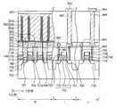
도 1 내지 도 6은 예시적인 실시예들에 따른 트랜지스터의 형성 방법을 설명하기 위한 단면도들이다.
도 7은 알루미늄 산화막을 열처리한 경우, 상기 알루미늄 산화막이 갖는 스트레스의 변화를 나타낸 그래프이다.
도 8은 다른 실시예들에 따른 트랜지스터의 형성 방법을 설명하기 위한 단면도이다.
도 9는 또 다른 실시예들에 따른 트랜지스터의 형성 방법을 설명하기 위한 단면도이다.
도 10 내지 도 13은 또 다른 실시예들에 따른 트랜지스터의 형성 방법을 설명하기 위한 단면도이다.
도 14는 또 다른 실시예들에 따른 트랜지스터의 형성 방법을 설명하기 위한 단면도이다.
도 15 내지 도 19는 또 다른 실시예들에 따른 트랜지스터 형성 방법을 설명하기 위한 단면도들이다.
도 20 및 도 21은 또 다른 실시예들에 따른 트랜지스터 형성 방법을 설명하기 위한 단면도들이다.
도 22 내지 도 23은 또 다른 실시예들에 따른 트랜지스터 형성 방법을 설명하기 위한 단면도들이다.
도 24 내지 도 30은 예시적인 실시예들에 따른 상보형 트랜지스터를 형성하는 방법을 설명하기 위한 단면도들이다.
도 31 내지 도 37은 예시적인 실시예들에 따른 반도체 소자를 제조하는 방법을 설명하기 위한 단면도들이다.1 to 6 are cross-sectional views illustrating a method of forming a transistor in accordance with example embodiments.
7 is a graph showing a change in stress of the aluminum oxide film when the aluminum oxide film is heat treated.
8 is a cross-sectional view illustrating a method of forming a transistor in accordance with other embodiments.
9 is a cross-sectional view for describing a method of forming a transistor according to still other embodiments.
10 to 13 are cross-sectional views illustrating a method of forming a transistor according to still other embodiments.
14 is a cross-sectional view for describing a method of forming a transistor according to still other embodiments.
15 to 19 are cross-sectional views illustrating a method of forming a transistor in accordance with still other embodiments.
20 and 21 are cross-sectional views illustrating a method of forming a transistor in accordance with still other embodiments.
22 to 23 are cross-sectional views illustrating a method of forming a transistor according to still other embodiments.
24 to 30 are cross-sectional views illustrating a method of forming a complementary transistor according to example embodiments.
31 to 37 are cross-sectional views illustrating a method of manufacturing a semiconductor device in accordance with example embodiments.
이하, 첨부된 도면들을 참조하여 본 발명의 바람직한 실시예들에 따른 트랜지스터 형성 방법, 상보형 트랜지스터 형성 방법 및 이를 이용한 반도체 소자 제조 방법에 대하여 상세하게 설명하지만, 본 발명이 하기의 실시예들에 제한되는 것은 아니며, 해당 분야에서 통상의 지식을 가진 자라면 본 발명의 기술적 사상을 벗어나지 않는 범위 내에서 본 발명을 다양한 다른 형태로 구현할 수 있을 것이다. 첨부된 도면에 있어서, 기판, 층(막), 영역, 패턴들 또는 구조물들의 치수는 본 발명의 명확성을 기하기 위하여 실제보다 확대하여 도시한 것이다. 본 발명에 있어서, 각 층(막), 영역, 전극, 패턴들 또는 구조물들이 기판, 각 층(막), 영역, 전극, 구조물들 또는 패턴들 "상에", "상부에" 또는 "하부"에 형성되는 것으로 언급되는 경우에는 각 층(막), 영역, 전극, 패턴들 또는 구조물들이 직접 기판, 각 층(막), 영역, 구조물 또는 패턴들 위에 형성되거나 아래에 위치하는 것을 의미하거나, 다른 층(막), 다른 영역, 다른 전극, 다른 패턴들 또는 다른 구조물이 기판 상에 추가적으로 형성될 수 있다. 또한, 물질, 층(막), 영역, 전극, 패턴들 또는 구조물들이 "제1", "제2" 및/또는 "예비"로 언급되는 경우, 이러한 부재들을 한정하기 위한 것이 아니라 단지 각 물질, 층(막), 영역, 전극, 패턴들 또는 구조물들을 구분하기 위한 것이다. 따라서 "제1", "제2" 및/또는 "예비"는 각 층(막), 영역, 전극, 패턴들 또는 구조물들에 대하여 각기 선택적으로 또는 교환적으로 사용될 수 있다.Hereinafter, a method of forming a transistor, a method of forming a complementary transistor, and a method of manufacturing a semiconductor device using the same according to exemplary embodiments of the present invention will be described in detail with reference to the accompanying drawings, but the present invention is limited to the following embodiments. Those skilled in the art will appreciate that the present invention may be embodied in various other forms without departing from the spirit of the invention. In the accompanying drawings, the dimensions of the substrates, layers (films), regions, patterns or structures are shown to be larger than actual for clarity of the invention. In the present invention, each layer (film), region, electrode, patterns or structures may be "on", "top" or "bottom" of the substrate, each layer (film), region, electrode, structures or patterns. When referred to as being formed in, it means that each layer (film), region, electrode, pattern or structure is formed directly over or below the substrate, each layer (film), region, structure or pattern, or otherwise Layers (films), other regions, other electrodes, other patterns or other structures may additionally be formed on the substrate. In addition, where materials, layers (films), regions, electrodes, patterns or structures are referred to as "first", "second" and / or "preliminary", it is not intended to limit these members, but only to each material, To distinguish between layers (films), regions, electrodes, patterns or structures. Thus, "first", "second" and / or "spare" may be used selectively or interchangeably for each layer (film), region, electrode, pattern or structure, respectively.
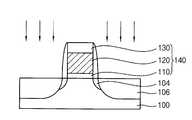
도 1 내지 도 6은 예시적인 실시예들에 따른 트랜지스터의 형성 방법을 설명하기 위한 단면도들이고, 도 7은 알루미늄 산화막을 열처리한 경우, 상기 알루미늄 산화막이 갖는 스트레스의 변화를 나타낸 그래프이다.1 to 6 are cross-sectional views illustrating a method of forming a transistor according to example embodiments, and FIG. 7 is a graph showing a change in stress of the aluminum oxide film when the aluminum oxide film is heat treated.
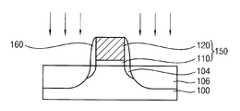
도 1을 참조하면, 기판(100) 상에 게이트 구조물(140)을 형성한다.Referring to FIG. 1, a
기판(100)은 실리콘 기판, 게르마늄 기판 혹은 실리콘-게르마늄 기판 등과 같은 반도체 기판이나, 실리콘-온-인슐레이터(Silicon-On-Insulator: SOI) 기판 혹은 게르마늄-온-인슐레이터(Germanium-On-Insulator: GOI) 기판 등을 포함할 수 있다. 한편, 도시하지는 않았으나, 기판(100)은 p형 혹은 n형 불순물을 포함하는 웰(well) 영역을 더 포함할 수 있다.The
게이트 구조물(140)은 기판(100) 상에 게이트 절연막, 게이트 도전막 및 게이트 마스크 층을 순차적으로 형성한 후, 사진 식각 공정을 이용하여 이들을 패터닝 함으로써 형성할 수 있다. 이에 따라, 게이트 구조물(140)은 기판(100) 상에 순차적으로 적층된 게이트 절연막 패턴(110), 게이트 전극(120) 및 게이트 마스크(130)를 포함하도록 형성될 수 있다.The
구체적으로, 상기 게이트 절연막은 실리콘 산화물과 같은 산화물 혹은 실리콘 산질화물과 같은 산질화물을 사용하여 형성할 수 있다. 상기 게이트 절연막은 기판(100)에 대해 열산화 공정을 수행하거나, 화학 기상 증착(Chemical Vapor Deposition: CVD) 공정을 수행하여 형성할 수 있다. 상기 게이트 도전막은 도핑된 폴리실리콘, 금속, 금속 질화물 및/또는 금속 실리사이드를 사용하여 형성할 수 있으며, 상기 게이트 마스크 층은 실리콘 질화물 혹은 실리콘 산질화물을 사용하여 형성할 수 있다. 상기 게이트 도전막 및 상기 게이트 마스크 층은 CVD 공정, 물리 기상 증착(Physical Vapor Deposition: PVD) 공정, 원자층 증착(Atomic Layer Deposition: ALD) 공정 등을 사용하여 형성할 수 있다.Specifically, the gate insulating layer may be formed using an oxide such as silicon oxide or an oxynitride such as silicon oxynitride. The gate insulating layer may be formed by performing a thermal oxidation process on the
게이트 구조물(140)을 이온 주입 마스크로 사용하여 기판(100) 상부에 이온을 주입함으로써, 게이트 구조물(140)에 인접한 기판(100) 상부에 비정질 이온 주입 영역(102)을 형성한다. 예시적인 실시예들에 따르면, 기판(100) 상부에 실리콘 혹은 게르마늄 이온을 주입할 수 있다. 상기 이온을 주입함에 따라, 기판(100)의 상부가 비정질화 되므로, 비정질 이온 주입 영역(102)이 형성될 수 있다.By implanting ions onto the
예시적인 실시예들에 따르면, 게이트 구조물(140)을 이온 주입 마스크로 사용하여 기판(100) 상부에 제2 불순물을 주입함으로써, 게이트 구조물(140)에 인접한 기판(100) 상부에 제2 불순물 영역(도시하지 않음)을 더 형성할 수 있다. 상기 제2 불순물은 인, 비소 등과 같은 n형 불순물일 수 있다. 일 실시예에 따르면, 상기 제2 불순물 영역은 비정질 이온 주입 영역 (102) 내에 형성될 수 있다. 이와는 달리, 상기 제2 불순물 영역은 비정질 이온 주입 영역(102)을 포함하도록 형성될 수도 있다.According to example embodiments, the second impurity region is formed on the
한편, 상기 제2 불순물 영역을 형성하는 공정은 비정질 이온 주입 영역(102) 형성 공정과 동시에 혹은 그 이전에 수행될 수도 있다.Meanwhile, the process of forming the second impurity region may be performed simultaneously with or before the process of forming the amorphous
도 2를 참조하면, 게이트 구조물(140)의 측벽 상에 스페이서(160)를 형성한다. 구체적으로, 게이트 마스크(130), 게이트 전극(120) 및 게이트 절연막 패턴(110)을 커버하는 스페이서 막을 형성한 후, 상기 스페이서 막을 이방성 식각 공정을 통해 부분적으로 제거함으로써 스페이서(160)를 형성할 수 있다. 상기 스페이서 막은 실리콘 질화물과 같은 질화물을 사용하여 형성할 수 있다.Referring to FIG. 2,
도 3을 참조하면, 기판(100) 상에 인장 스트레스를 갖는 제1 인장 스트레스 막(170) 및 제2 인장 스트레스 막(180)을 순차적으로 형성한다. 예시적인 실시예들에 따르면, 제1 및 제2 인장 스트레스 막들(170, 180)은 게이트 구조물(140) 및 스페이서(160)를 커버하도록 기판(100) 상에 형성될 수 있다. 제1 인장 스트레스 막(170)은 제2 인장 스트레스 막(180)보다 작은 두께를 갖도록 형성될 수 있으며, 일 실시예에 따르면, 대략 10 내지 120 옹스트롱의 두께를 갖도록 형성될 수 있다.Referring to FIG. 3, the first
제1 인장 스트레스 막(170)은 알루미늄 산화물(Al2O3), 금속 실리케이트 혹은 금속 실리콘 산질화물을 사용하여 형성될 수 있다. 예를 들어, 제1 인장 스트레스 막(170)은 알루미늄 산화물, 하프늄 실리케이트(HfSiO), 지르코늄 실리케이트(ZrSiO), 란탄 실리케이트(LaSiO), 하프늄 실리콘 산질화물(HfSiON) 혹은 지르코늄 실리콘 산질화물(ZrSiON)을 사용하여 형성될 수 있다.The first
한편, 제2 인장 스트레스 막(180)은 실리콘 질화물을 사용하여 형성될 수 있다.Meanwhile, the second
도 4를 참조하면, 제1 및 제2 인장 스트레스 막들(170, 180)이 형성된 기판(100)을 열처리하여, 비정질 이온 주입 영역(102)에 스트레스를 기억시킨다. 즉, 비정질 이온 주입 영역(102) 상에 인장 스트레스를 갖는 제1 및 제2 인장 스트레스 막들(170, 180)이 형성된 상태에서 상기 열처리를 함에 따라, 비정질 이온 주입 영역(106)이 재결정화되어 결정질 이온 주입 영역(106)이 형성되며, 이때 결정질 이온 주입 영역(106)은 압축 스트레스를 갖게 된다. 결과적으로, 이후 상기 트랜지스터의 채널 영역으로 기능하는 결정질 이온 주입 영역(106) 사이의 기판(100) 상부는 인장 스트레스를 갖게 된다.Referring to FIG. 4, the
예시적인 실시예들에 따르면, 상기 열처리는 제1 인장 스트레스 막(170)의 결정화 온도보다 낮은 온도에서 수행된다. 예를 들어, 제1 인장 스트레스 막(170)이 알루미늄 산화물을 포함하는 경우, 상기 열처리는 대략 섭씨 800도 이하에서 수행될 수 있다.According to exemplary embodiments, the heat treatment is performed at a temperature lower than the crystallization temperature of the first
도 5를 참조하면, 제1 및 제2 인장 스트레스 막들(170, 180)을 제거한다.Referring to FIG. 5, the first and second
예시적인 실시예들에 따르면, 인산(H2PO3)을 포함하는 식각액을 사용하여 제2 인장 스트레스 막(180)을 제거하고, 불화수소(HF)를 포함하는 식각액을 사용하여 제1 인장 스트레스 막(170)을 제거한다. 예를 들어, 제1 인장 스트레스 막(170)이 알루미늄 산화물을 포함하고 대략 섭씨 630도에서 열처리된 경우, 제1 인장 스트레스 막(170)은 200:1로 희석한 불화수소 식각액에 대해 대략 2.3 옹스트롱/초의 높은 식각률을 가지며, 이는 상기 식각액에 대한 실리콘 산화막의 식각률과 유사한 값이다. 이와는 달리, 제1 및 제2 인장 스트레스 막들(170, 180)은 건식 식각 공정으로 제거될 수도 있다.According to example embodiments, the second
한편, 인산 식각액을 사용하여 제2 인장 스트레스 막(180)을 제거할 때, 실리콘 질화물을 포함하는 게이트 마스크(130) 및 스페이서(140)는 제1 인장 스트레스 막(170)에 의해 커버되어 보호될 수 있다. 즉, 제1 인장 스트레스 막(170)은 상기 인산 식각액에 대한 일종의 식각 저지막으로서 기능할 수 있다. 또한, 제1 인장 스트레스 막(170)은 실리콘 질화물에 대해 낮은 식각률을 갖는 불화수소(HF) 식각액에 의해 제거되므로, 제1 인장 스트레스 막(170)이 제거될 때 게이트 마스크(130) 및 스페이서(140)는 손상되지 않을 수 있다.Meanwhile, when the second
도 6을 참조하면, 게이트 구조물(140) 및 스페이서(160)를 이온 주입 마스크로 사용하여 제1 불순물을 기판(100) 상부에 주입함으로써, 게이트 구조물(140)에 인접한 기판(100) 상부에 제1 불순물 영역(106)을 형성한다. 예시적인 실시예들에 따르면, 제1 불순물 영역(106)은 결정질 이온 주입 영역(104)보다 깊은 깊이를 갖도록 형성될 수 있다. 한편, 상기 제1 불순물을 주입한 후, 열처리 공정을 더 수행할 수 있다.Referring to FIG. 6, a first impurity is implanted into the
예시적인 실시예들에 따르면, 상기 제1 불순물은 인 혹은 비소와 같은 n형 불순물일 수 있다. 상기 제1 불순물은 상기 제2 불순물에 비해 높은 농도를 가질 수 있으며, 이에 따라 제1 불순물 영역(106) 및 상기 제2 불순물 영역은 엘디디(Lightly Doped Drain: LDD) 구조를 갖는 불순물 영역을 형성할 수 있다. 상기 불순물 영역은 상기 트랜지스터의 소스/드레인 영역으로서 기능할 수 있다.In example embodiments, the first impurity may be an n-type impurity such as phosphorous or arsenic. The first impurity may have a higher concentration than the second impurity, and thus, the
전술한 공정들을 수행함으로써, 상기 트랜지스터가 완성된다. 상기 트랜지스터의 형성 과정에서, 게이트 구조물(140)에 인접한 기판(100) 상부에 비정질 이온 주입 영역(102)을 형성하고, 제1 및 제2 인장 스트레스 막들(170, 180)을 기판(100) 상에 형성한다. 이후, 기판(100)을 열처리하여 비정질 이온 주입 영역(102)에 스트레스를 인가함으로써, 압축 스트레스를 갖는 결정질 이온 주입 영역(104)을 형성하며, 이에 따라 상기 소스/드레인 영역 사이에 형성되는 채널 영역은 인장 스트레스를 가질 수 있다.By performing the above-described processes, the transistor is completed. In the process of forming the transistor, an amorphous
도 7을 참조하면, 알루미늄 산화물을 포함하는 제1 인장 스트레스 막(170)은 열처리 이전에도 인장 스트레스를 가지며, 예를 들어, 대략 12nm의 두께를 갖는 경우, 대략 섭씨 600도에서 열처리된 후 대략 1.2GPa의 인장 스트레스를 가지고, 대략 섭씨 800도에서 열처리된 후 대략 3.2GPa의 인장 스트레스를 갖는다. 이는 실리콘 산화물을 포함하는 인장 스트레스 막이 열처리 이전 대략 0.05GPa의 압축 스트레스를 가지고, 대략 섭씨 600도의 열처리 이후 대략 0.12GPa의 인장 스트레스를 가지는 것에 비해 훨씬 큰 인장 스트레스를 갖는 것이다. 이와 같이, 제1 인장 스트레스 막(170)이 큰 인장 스트레스를 가짐에 따라, 상기 트랜지스터의 채널 영역 역시 큰 인장 스트레스를 가질 수 있다. 이에 따라, 상기 채널 영역의 전자의 이동도가 향상되며, 결과적으로 상기 트랜지스터는 향상된 구동 전류 특성 및 동작 속도를 가질 수 있다. 또한, 실리콘 질화물을 포함하는 제2 인장 스트레스 막(180)이 제1 인장 스트레스 막(170)과 함께 사용되는 경우, 상기 채널 영역은 더 큰 인장 스트레스를 가질 수 있다.Referring to FIG. 7, the first
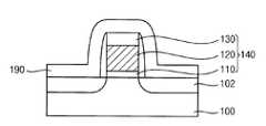
도 8은 다른 실시예들에 따른 트랜지스터의 형성 방법을 설명하기 위한 단면도이다. 상기 트랜지스터의 형성 방법은 인장 스트레스 막을 제외하고는 도 1 내지 도 6을 참조로 설명한 트랜지스터 형성 방법과 실질적으로 동일하거나 유사하므로, 동일한 구성 요소에는 동일한 참조 부호를 부여하고 중복 설명은 생략한다.8 is a cross-sectional view illustrating a method of forming a transistor in accordance with other embodiments. Since the method of forming the transistor is substantially the same as or similar to the method of forming the transistor described with reference to FIGS. 1 to 6 except for the tensile stress film, the same components are assigned the same reference numerals and redundant descriptions are omitted.
먼저, 도 1 내지 도 2를 참조로 설명한 공정들을 수행한다.First, the processes described with reference to FIGS. 1 to 2 are performed.
도 8을 참조하면, 기판(100) 상에 제3 인장 스트레스 막(190)을 형성한다.Referring to FIG. 8, a third
제3 인장 스트레스 막(190)은 제1 인장 스트레스 막(170)과 실질적으로 동일한 물질을 사용하여 형성될 수 있다. 즉, 제3 인장 스트레스 막(190)은 알루미늄 산화물(Al2O3), 금속 실리케이트 혹은 금속 실리콘 산질화물을 사용하여 형성될 수 있다. 일 실시예에 따르면, 제3 인장 스트레스 막(190)은 대략 10 내지 250 옹스트롱의 두께를 갖도록 형성될 수 있다.The third
이후, 도 4 및 도 5를 참조로 설명한 공정들을 수행한다.Thereafter, the processes described with reference to FIGS. 4 and 5 are performed.
즉, 제3 인장 스트레스 막(190)이 형성된 기판(100)을 제3 인장 스트레스 막(190)의 결정화 온도보다 낮은 온도에서 열처리한다. 예를 들어, 제3 인장 스트레스 막(190)이 알루미늄 산화물을 포함하는 경우, 상기 열처리는 대략 섭씨 800도 이하에서 수행될 수 있다. 이후, 제3 인장 스트레스 막(190)을 제거한다. 예시적인 실시예들에 따르면, 불화수소(HF)를 포함하는 식각액을 사용하여 제3 인장 스트레스 막(190)을 제거한다. 제3 인장 스트레스 막(190)은 실리콘 질화물에 대해 낮은 식각률을 갖는 불화수소(HF) 식각액에 의해 제거되므로, 제3 인장 스트레스 막(190)이 제거될 때 게이트 마스크(130) 및 스페이서(140)는 제거되지 않을 수 있다. 이와는 달리, 제3 인장 스트레스 막(190)은 건식 식각 공정으로 제거될 수도 있다.That is, the
이후 도 6을 참조로 설명한 공정들을 수행하여 상기 트랜지스터를 형성할 수 있다.Thereafter, the transistors may be formed by performing the processes described with reference to FIG. 6.
상기 트랜지스터 형성 공정에서, 높은 인장 스트레스를 갖는 제3 인장 스트레스 막(190)을 통해 비정질 이온 주입 영역(102)에 스트레스를 인가하므로, 상기 트랜지스터의 채널 영역이 큰 인장 스트레스를 가질 수 있다. 또한 제3 인장 스트레스 막(190)은 불화수소 식각액에 의해 용이하게 제거되므로 실리콘 질화물을 포함하는 게이트 마스크(130)나 스페이서(160)가 손상되지 않을 수 있다.In the transistor forming process, since the stress is applied to the amorphous ion implanted
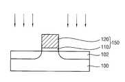
도 9는 또 다른 실시예들에 따른 트랜지스터의 형성 방법을 설명하기 위한 단면도이다. 상기 트랜지스터의 형성 방법은 인장 스트레스 막을 제외하고는 도 1 내지 도 6을 참조로 설명한 트랜지스터 형성 방법과 실질적으로 동일하거나 유사하므로, 동일한 구성 요소에는 동일한 참조 부호를 부여하고 중복 설명은 생략한다.9 is a cross-sectional view for describing a method of forming a transistor according to still other embodiments. Since the method of forming the transistor is substantially the same as or similar to the method of forming the transistor described with reference to FIGS. 1 to 6 except for the tensile stress film, the same components are assigned the same reference numerals and redundant descriptions are omitted.
먼저, 도 1 내지 도 2를 참조로 설명한 공정들을 수행한다.First, the processes described with reference to FIGS. 1 to 2 are performed.
도 9를 참조하면, 게이트 구조물(140) 및 스페이서(160)를 커버하도록 기판(100) 상에 식각 저지막(200) 및 제4 인장 스트레스 막(210)을 순차적으로 형성한다. 예시적인 실시예들에 따르면, 제4 인장 스트레스 막(210)은 식각 저지막(200)에 비해 큰 두께를 갖도록 형성될 수 있다.Referring to FIG. 9, an
식각 저지막(200)은 실리콘 산화물을 사용하여 형성될 수 있다. 제4 인장 스트레스 막(210)은 제1 인장 스트레스 막(170)과 실질적으로 동일한 물질을 사용하여 형성될 수 있다. 즉, 제4 인장 스트레스 막(210)은 알루미늄 산화물(Al2O3), 금속 실리케이트 혹은 금속 실리콘 산질화물을 사용하여 형성될 수 있다.The
이후, 제4 인장 스트레스 막(210)의 결정화 온도보다 높은 온도에서 식각 저지막(200) 및 제4 인장 스트레스 막(210)이 형성된 기판(100)을 열처리한다. 예를 들어, 제4 인장 스트레스 막(210)이 알루미늄 산화물을 포함하는 경우, 상기 열처리는 대략 섭씨 800도 이상에서 수행될 수 있다.Thereafter, the
이후, 제4 인장 스트레스 막(210) 및 식각 저지막(200)을 제거한다. 예시적인 실시예들에 따르면, 인산(H2PO3)을 포함하는 식각액을 사용하여 제4 인장 스트레스 막(210)을 제거하고, 불화수소(HF)를 포함하는 식각액을 사용하여 식각 저지막(190)을 제거한다. 상기 인산 식각액을 사용하여 제4 인장 스트레스 막(210)을 제거할 때, 실리콘 질화물을 포함하는 게이트 마스크(130) 및 스페이서(140)는 식각 저지막(200)에 의해 커버되어 보호될 수 있다. 또한, 식각 저지막(200)은 실리콘 질화물에 대해 낮은 식각률을 갖는 불화수소(HF) 식각액에 의해 제거되므로, 식각 저지막(200)이 제거될 때 게이트 마스크(130) 및 스페이서(140)는 제거되지 않을 수 있다. 이와는 달리, 제4 인장 스트레스 막(210) 및 식각 저지막(200)은 건식 식각 공정으로도 제거될 수도 있다.Thereafter, the fourth
이후 도 6을 참조로 설명한 공정들을 수행하여 상기 트랜지스터를 형성할 수 있다.Thereafter, the transistors may be formed by performing the processes described with reference to FIG. 6.
상기 트랜지스터 형성 공정에서, 제4 인장 스트레스 막(210)은 결정화 온도 이상에서 열처리되므로, 보다 큰 인장 스트레스를 가질 수 있다. 이에 따라, 상기 트랜지스터의 채널 영역은 큰 인장 스트레스를 가질 수 있다. 또한 제4 인장 스트레스 막(210)이 제거될 때, 식각 저지막(200)이 게이트 마스크(130) 및 스페이서(160)를 커버하여 보호할 수 있다.In the transistor forming process, since the fourth
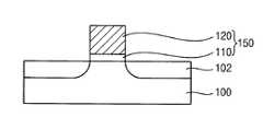
도 10 내지 도 13은 또 다른 실시예들에 따른 트랜지스터의 형성 방법을 설명하기 위한 단면도이다. 상기 트랜지스터의 형성 방법은 게이트 구조물 및 스페이서를 제외하고는 도 1, 도 3 내지 도 6을 참조로 설명한 트랜지스터 형성 방법과 유사하므로, 동일한 구성 요소에는 동일한 참조 부호를 부여하고 중복 설명은 생략한다.10 to 13 are cross-sectional views illustrating a method of forming a transistor according to still other embodiments. Since the method of forming the transistor is similar to the method of forming the transistor described with reference to FIGS. 1 and 3 to 6 except for the gate structure and the spacer, the same reference numeral is given to the same component and the description thereof will be omitted.
도 10을 참조하면, 기판(100) 상에 게이트 구조물(150)을 형성한다.Referring to FIG. 10, the
구체적으로, 기판(100) 상에 게이트 절연막, 게이트 도전막 및 게이트 마스크 층을 순차적으로 형성한 후, 포토레지스트 패턴(도시하지 않음)을 상기 게이트 마스크 층 상에 형성한다. 상기 포토레지스트 패턴을 식각 마스크로 사용하는 식각 공정을 통해 상기 게이트 마스크 층을 패터닝 하여 게이트 마스크를 형성한다. 상기 포토레지스트 패턴을 제거한 후, 상기 게이트 마스크를 식각 마스크로 사용하는 식각 공정을 통해 상기 게이트 도전막 및 상기 게이트 절연막을 패터닝 한다. 이때, 상기 게이트 마스크가 제거될 수 있으며, 이에 따라 기판(100) 상에 순차적으로 적층된 게이트 절연막 패턴(110) 및 게이트 전극(120)을 포함하는 게이트 구조물(150)이 형성될 수 있다.Specifically, after the gate insulating film, the gate conductive film and the gate mask layer are sequentially formed on the
도 11을 참조하면, 기판(100) 상에 제4 인장 스트레스 막(210)을 형성한다.Referring to FIG. 11, a fourth
이후, 도 4를 참조로 설명한 공정과 유사한 공정을 수행한다. 다만, 제4 인장 스트레스 막(210)의 결정화 온도보다 높은 온도에서 제4 인장 스트레스 막(210)이 형성된 기판(100)을 열처리한다.Thereafter, a process similar to the process described with reference to FIG. 4 is performed. However, the
도 12를 참조하면, 도 5를 참조로 설명한 공정과 유사한 공정을 수행한다. 다만, 인산을 포함하는 식각액을 사용하여 제4 인장 스트레스 막(210)을 제거할 수 있다. 이때, 게이트 구조물(150)은 게이트 마스크를 포함하고 있지 않으며, 또한 게이트 구조물(150) 측벽 상에는 스페이서가 형성되어 있지 않다. 이에 따라, 상기 인산 식각액을 사용하여 제4 인장 스트레스 막(210)을 제거하더라도, 게이트 구조물(150)은 손상되지 않을 수 있다. 이와는 달리, 제4 인장 스트레스 막(210)은 건식 식각 공정으로도 제거될 수도 있다.Referring to FIG. 12, a process similar to the process described with reference to FIG. 5 is performed. However, the fourth
이후 도 6을 참조로 설명한 공정들과 유사한 공정들을 수행한다. 다만, 제1 불순물 영역(106)을 형성하기 이전에, 게이트 구조물(150)의 측벽 상에 실리콘 질화물을 사용하여 스페이서(160)를 형성한다. 이에 따라, 상기 트랜지스터를 형성할 수 있다.Thereafter, processes similar to those described with reference to FIG. 6 are performed. However, before forming the
상기 트랜지스터 형성 공정에서, 제4 인장 스트레스 막(210)은 결정화 온도 이상에서 열처리되므로, 보다 큰 인장 스트레스를 가질 수 있다. 한편, 제4 인장 스트레스 막(210)을 제거할 때, 게이트 구조물(150)과 제4 인장 스트레스 막(210) 사이에 별도의 식각 저지막이 형성되지 않더라도, 게이트 구조물(150)은 게이트 마스크를 포함하지 않고 또한 게이트 구조물(150)에는 스페이서가 형성되어 있지 않으므로, 게이트 구조물(150)이 손상되지 않을 수 있다.In the transistor forming process, since the fourth
도 14는 또 다른 실시예들에 따른 트랜지스터의 형성 방법을 설명하기 위한 단면도이다. 상기 트랜지스터는 도 10 내지 도 13을 참조로 설명한 트랜지스터 형성 방법에서, 제4 인장 스트레스 막(210) 상에 실리콘 질화물을 포함하는 제2 인장 스트레스 막(180)을 더 형성하는 것을 제외하고는 실질적으로 동일하거나 유사하다.14 is a cross-sectional view for describing a method of forming a transistor according to still other embodiments. The transistor is substantially the same as the transistor forming method described with reference to FIGS. 10 to 13 except for further forming a second
즉, 인산 식각액을 사용하여 제2 및 제4 인장 스트레스 막들(180, 210)을 제거할 때, 게이트 구조물(150)은 게이트 마스크를 포함하고 있지 않고 또한 게이트 구조물(150) 측벽 상에는 스페이서도 형성되어 있지 않으므로, 게이트 구조물(150)은 손상되지 않을 수 있다. 한편, 제2 및 제4 인장 스트레스 막들(180, 210)을 함께 형성함에 따라, 상기 트랜지스터의 채널 영역은 큰 인장 스트레스를 가질 수 있다.That is, when the second and fourth
도 15 내지 도 19는 또 다른 실시예들에 따른 트랜지스터 형성 방법을 설명하기 위한 단면도들이다. 상기 트랜지스터의 형성 방법은 게이트 구조물을 제외하고는 도 1 내지 도 6을 참조로 설명한 트랜지스터 형성 방법과 실질적으로 동일하거나 유사하므로, 동일한 구성 요소에는 동일한 참조 부호를 부여하고 중복 설명은 생략한다.15 to 19 are cross-sectional views illustrating a method of forming a transistor in accordance with still other embodiments. Since the method of forming the transistor is substantially the same as or similar to the method of forming the transistor described with reference to FIGS. 1 to 6 except for the gate structure, the same components are assigned the same reference numerals, and description thereof will not be repeated.
도 15를 참조하면, 기판(300) 상부에 리세스(305)를 형성한다.Referring to FIG. 15, a
예시적인 실시예들에 따르면, 기판(300) 상에 패드 산화막(도시하지 않음) 및 하드 마스크(도시하지 않음)를 순차적으로 형성하고, 상기 하드 마스크를 식각 마스크로 사용하여 상기 패드 산화막 및 기판(300) 상부를 식각한다. 상기 식각 공정은 이방성 식각 공정을 통해 수행될 수 있다. 일 실시예에 따르면, 상기 이방성 식각 공정 이후에 등방성 식각 공정을 더 수행하여, 리세스(305) 하부가 라운딩될 수 있다. 이후, 상기 하드 마스크 및 상기 패드 산화막은 제거된다.In example embodiments, a pad oxide layer (not shown) and a hard mask (not shown) may be sequentially formed on the
도 16을 참조하면, 리세스(305)의 내벽 및 기판(300) 상면에 게이트 절연막(310)을 형성하고, 리세스(305)의 나머지를 채우는 게이트 도전막(320)을 게이트 절연막(310) 상에 형성한다. 게이트 도전막(320) 상에는 게이트 마스크 층(330)을 형성한다.Referring to FIG. 16, a
도 17을 참조하면, 사진 식각 공정을 통해, 게이트 마스크 층(330), 게이트 도전막(320) 및 게이트 절연막(310)을 패터닝 함으로써 게이트 구조물(340)을 형성할 수 있다. 이에 따라, 게이트 구조물(340)은 기판(300)의 리세스(305) 내벽 상에 형성된 게이트 절연막 패턴(312)과, 게이트 절연막 패턴(312) 상에 순차적으로 적층된 게이트 전극(322) 및 게이트 마스크(332)를 포함하도록 형성될 수 있다.Referring to FIG. 17, the
이후, 게이트 구조물(340)을 이온 주입 마스크로 사용하여 기판(300) 상부에 이온을 주입함으로써, 게이트 구조물(340)에 인접한 기판(300) 상부에 비정질 이온 주입 영역(302)을 형성한다. 예시적인 실시예들에 따르면, 비정질 이온 주입 영역(302)은 게이트 구조물(340)보다 작은 깊이를 갖도록 형성될 수 있다.Thereafter, by implanting ions into the
예시적인 실시예들에 따르면, 게이트 구조물(340)을 이온 주입 마스크로 사용하여 기판(300) 상부에 제2 불순물을 주입함으로써, 게이트 구조물(340)에 인접한 기판(300) 상부에 제2 불순물 영역(도시하지 않음)을 더 형성할 수 있다. 상기 제2 불순물은 인, 비소 등과 같은 n형 불순물일 수 있다. 일 실시예에 따르면, 상기 제2 불순물 영역은 비정질 이온 주입 영역(302) 내에 형성될 수 있다. 이와는 달리, 상기 제2 불순물 영역은 비정질 이온 주입 영역(302)을 포함하도록 형성될 수도 있다.According to example embodiments, the second impurity region is formed on the
한편, 상기 제2 불순물 영역을 형성하는 공정은 비정질 이온 주입 영역(302) 형성 공정과 동시에 혹은 그 이전에 수행될 수도 있다.Meanwhile, the process of forming the second impurity region may be performed simultaneously with or before the process of forming the amorphous
도 18을 참조하면, 도 2 내지 도 4를 참조로 설명한 공정들과 실질적으로 동일하거나 유사한 공정들을 수행한다.Referring to FIG. 18, the processes substantially the same as or similar to those described with reference to FIGS. 2 to 4 are performed.
즉, 게이트 구조물(340)의 측벽 상에 스페이서(360)를 형성하고, 게이트 구조물(340) 및 스페이서(360)를 커버하도록 기판(300) 상에 제1 인장 스트레스 막(370) 및 제2 인장 스트레스 막(380)을 순차적으로 형성한다. 이후, 제1 및 제2 인장 스트레스 막들(370, 380)이 형성된 기판(300)을 열처리하여, 비정질 이온 주입 영역(302)을 압축 스트레스를 갖는 결정질 이온 주입 영역(304)으로 변환시킨다.That is, the
도 19를 참조하면, 제2 및 제1 인장 스트레스 막들(380, 370)을 각각 인산(H2PO3)을 포함하는 식각액 불화수소(HF)를 포함하는 식각액을 사용하여 제거한다. 이후, 게이트 구조물(340) 및 스페이서(360)를 이온 주입 마스크로 사용하여 제1 불순물을 기판(300) 상부에 주입함으로써, 게이트 구조물(340)에 인접한 기판(300) 상부에 제1 불순물 영역(306)을 형성한다. 일 실시예에 따르면, 제1 불순물 영역(306)은 결정질 이온 주입 영역(304)을 포함하고, 결정질 이온 주입 영역(304)보다 깊은 깊이를 갖도록 형성된다. 이에 따라, 상기 트랜지스터가 완성된다.Referring to FIG. 19, the second and first
도 20 및 도 21은 또 다른 실시예들에 따른 트랜지스터 형성 방법을 설명하기 위한 단면도들이다. 도 20의 트랜지스터 형성 방법에서는, 도 8을 참조로 설명한 방법과 유사하게, 알루미늄 산화물을 포함하는 제3 인장 스트레스 막(390)을 기판(300) 상에 형성하고, 제3 인장 스트레스 막(390)의 결정화 온도보다 낮은 온도에서 열처리한다. 또한, 도 21의 트랜지스터 형성 방법에서는, 도 9를 참조로 설명한 방법과 유사하게, 실리콘 산화물을 포함하는 식각 저지막(400) 및 알루미늄 산화물을 포함하는 제4 인장 스트레스 막(410)을 기판(300) 상에 순차적으로 형성하고, 제4 인장 스트레스 막(410)의 결정화 온도보다 높은 온도에서 열처리한다.20 and 21 are cross-sectional views illustrating a method of forming a transistor in accordance with still other embodiments. In the transistor forming method of FIG. 20, similar to the method described with reference to FIG. 8, a third
한편, 도시하지는 않았지만, 결정질 이온 주입 영역(304) 형성 공정 이후에 스페이서(360)를 형성하는 경우, 도 10 내지 도 14를 참조로 설명한 트랜지스터 형성 방법을 적용하여 리세스 게이트 구조물을 갖는 트랜지스터를 형성할 수 있음은 당업자에게 자명하다.Although not shown, when the
도 22 내지 도 23은 또 다른 실시예들에 따른 트랜지스터 형성 방법을 설명하기 위한 단면도들이다.22 to 23 are cross-sectional views illustrating a method of forming a transistor according to still other embodiments.
먼저, 도 1 내지 도 5를 참조로 설명한 공정들과 실질적으로 동일한 공정들을 수행한다.First, substantially the same processes as those described with reference to FIGS. 1 to 5 are performed.
이후, 도 22를 참조하면, 기판(100) 상에 선택적 에피택시얼 성장 (Selective Epitaxial Growth: SEG) 공정을 수행하여 에피택시얼 층(108)을 형성한다. 에피택시얼 층(108)은 게이트 구조물(140) 및 스페이서(160)에 의해 커버되지 않는 기판(100) 상부를 씨드막으로 하여 형성된다.Thereafter, referring to FIG. 22, an
일 실시예에 따르면, 상기 SEG 공정은 약 700℃ 내지 약 900℃의 온도 및 약 10torr 내지 약 50torr의 압력에서 CVD 공정을 수행함으로써 형성될 수 있다. 상기 CVD 공정은 예를 들어, 디클로로실란(SiH2Cl2) 가스를 사용하여 수행할 수 있으며, 이에 따라 단결정 실리콘막이 형성될 수 있다. 혹은, 상기 SEG 공정은 감압 화학 기상 증착(Reduced Pressure CVD: RPCVD) 공정, 저압 화학 기상 증착(Low Pressure CVD: LPCVD) 공정, 초고진공 화학 기상 증착(Ultra High Vacuum CVD: UHVCVD) 공정, 유기 금속 화학 기상 증착(Metal Organic CVD: MOCVD) 공정 등을 통해 수행될 수도 있다. 일 실시예에 따르면, 에피택시얼 층(108)은 100Å 내지 500Å의 높이를 갖도록 형성된다.According to one embodiment, the SEG process may be formed by performing a CVD process at a temperature of about 700 ℃ to about 900 ℃ and a pressure of about 10 tor to about 50 tor. For example, the CVD process may be performed using dichlorosilane (SiH2 Cl2 ) gas, and thus a single crystal silicon film may be formed. Alternatively, the SEG process may include reduced pressure CVD (RPCVD) process, low pressure CVD (LPCVD) process, ultra high vacuum CVD (UHVCVD) process, and organometallic chemistry. It may also be carried out through a metal organic CVD (MOCVD) process. According to one embodiment,
도 23을 참조하면, 게이트 구조물(140) 및 스페이서(160)를 이온 주입 마스크로 사용하는 이온 주입 공정을 통해, 에피택시얼 층(108) 및 기판(100) 상부에 제1 불순물을 주입한다. 이에 따라 게이트 구조물(140)에 인접한 기판(100) 상부에는 제1 불순물 영역(106)이 형성되고, 에피택시얼 층(108)은 이른 바 올려진 소스/드레인(ESD) 층으로 기능할 수 있다. 즉, 에피택시얼 층(108) 및 제1 불순물 영역(108)은 함께 상기 트랜지스터의 소스/드레인 영역의 역할을 수행할 수 있다. 이와 같이 불순물이 도핑된 에피택시얼 층(108)을 ESD 층(109)으로 정의할 수 있다. 예시적인 실시예들에 따르면, 상기 제1 불순물은 인, 비소 등의 n형 불순물을 포함할 수 있다. 일 실시예에 따르면, 제1 불순물 영역(106)은 결정질 이온 주입 영역(104)보다 깊은 깊이를 갖도록 형성될 수 있다.Referring to FIG. 23, a first impurity is implanted into the
전술한 공정들을 수행함으로써 상기 트랜지스터가 완성된다.The transistor is completed by performing the above-described processes.
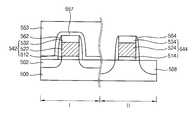
도 24 내지 도 30은 예시적인 실시예들에 따른 상보형 트랜지스터를 형성하는 방법을 설명하기 위한 단면도들이다. 상기 상보형 트랜지스터 형성 방법에서, NMOS 영역의 트랜지스터는 도 1 내지 도 6을 참조로 설명한 트랜지스터 형성 방법과 실질적으로 동일하거나 유사한 방법으로 형성되므로, 이에 대해서는 간략히 설명한다.24 to 30 are cross-sectional views illustrating a method of forming a complementary transistor according to example embodiments. In the above-described complementary transistor forming method, the transistor in the NMOS region is formed in substantially the same or similar method as the transistor forming method described with reference to FIGS. 1 to 6, which will be briefly described.
도 24를 참조하면, 기판(500)의 제1 영역(I) 및 제2 영역(II) 상에 제1 게이트 구조물(542) 및 제2 게이트 구조물(544)을 각각 형성한다. 예시적인 실시예들에 따르면, 기판(500)은 단결정 실리콘을 포함할 수 있다. 한편, 제1 영역(I)은 NMOS 영역일 수 있고, 제2 영역(II)은 PMOS 영역일 수 있다.Referring to FIG. 24, a
제1 및 제2 게이트 구조물들(542, 544)은 기판(500) 상에 게이트 절연막, 게이트 도전막 및 게이트 마스크 층을 순차적으로 형성한 후, 사진 식각 공정을 이용하여 이들을 패터닝 함으로써 형성할 수 있다. 이에 따라, 제1 게이트 구조물(542)은 기판(500)의 제1 영역(I) 상에 순차적으로 적층된 제1 게이트 절연막 패턴(512), 제1 게이트 전극(522) 및 제1 게이트 마스크(532)를 포함하도록 형성되고, 제2 게이트 구조물(544)은 기판(500)의 제2 영역(II) 상에 순차적으로 적층된 제2 게이트 절연막 패턴(514), 제2 게이트 전극(524) 및 제2 게이트 마스크(534)를 포함하도록 형성된다.The first and
제2 게이트 구조물(544)을 커버하는 제1 마스크(551)를 기판(500)의 제2 영역(II) 상에 형성하고, 제1 게이트 구조물(542)을 이온 주입 마스크로 사용하여 기판(500)의 제1 영역(I) 상부에 이온을 주입함으로써, 제1 게이트 구조물(542)에 인접한 기판(500) 상부에 비정질 이온 주입 영역(502)을 형성한다.A
한편, 제1 게이트 구조물(542)을 이온 주입 마스크로 사용하여 기판(500)의 제1 영역(I) 상부에 제2 불순물을 주입함으로써, 제1 게이트 구조물(542)에 인접한 기판(500) 상부에 제2 불순물 영역(도시하지 않음)을 더 형성할 수도 있다. 상기 제2 불순물은 인, 비소 등과 같은 n형 불순물일 수 있다.Meanwhile, the second impurity is implanted into the first region I of the
이후, 제1 마스크(551)는 제거된다.Thereafter, the
도 25를 참조하면, 제1 및 제2 게이트 구조물들(542, 544)의 측벽 상에 제1 스페이서(562) 및 제2 스페이서(564)를 각각 형성한다. 구체적으로, 제1 및 제2 게이트 구조물들(542, 544)을 커버하는 스페이서 막을 형성한 후, 상기 스페이서 막을 이방성 식각 공정을 통해 부분적으로 제거함으로써 제1 및 제2 스페이서들(562, 564)을 형성할 수 있다.Referring to FIG. 25, first and
이후, 기판(500) 상에 제1 인장 스트레스 막(570) 및 제2 인장 스트레스 막(580)을 순차적으로 형성한다. 예시적인 실시예들에 따르면, 제1 및 제2 인장 스트레스 막들(570, 580)은 제1 및 제2 게이트 구조물들(542, 544) 및 제1 및 제2 스페이서들(562, 564)을 커버하도록 기판(500) 상에 형성될 수 있다. 제1 인장 스트레스 막(570)은 알루미늄 산화물(Al2O3), 금속 실리케이트 혹은 금속 실리콘 산질화물을 사용하여 형성될 수 있으며, 제2 인장 스트레스 막(580)은 실리콘 질화물을 사용하여 형성될 수 있다.Thereafter, the first
제1 및 제2 인장 스트레스 막들(570, 580)이 형성된 기판(500)을 열처리하여, 비정질 이온 주입 영역(502)을 재결정화시켜 압축 스트레스를 갖는 결정질 이온 주입 영역(504)을 형성한다. 한편, 기판(500)의 제2 영역(II)은 단결정 실리콘을 포함하므로, 상기 열처리를 수행하더라도 스트레스의 변화가 크지 않을 수 있다.The
예시적인 실시예들에 따르면, 상기 열처리는 제1 인장 스트레스 막(570)의 결정화 온도보다 낮은 온도에서 수행될 수 있다.According to example embodiments, the heat treatment may be performed at a temperature lower than the crystallization temperature of the first
도 26을 참조하면, 제1 및 제2 인장 스트레스 막들(570, 580)을 제거한다. 제2 인장 스트레스 막(580)은 인산(H2PO3)을 포함하는 식각액을 사용하여 제거될 수 있고, 제1 인장 스트레스 막(570)은 불화수소(HF)를 포함하는 식각액을 사용하여 제거될 수 있다.Referring to FIG. 26, the first and second
도 27을 참조하면, 제1 및 제2 게이트 구조물들(542, 544) 및 제1 및 제2 스페이서들(562, 564)을 커버하는 성장 방지막(557)을 형성한다. 예시적인 실시예들에 따르면, 성장 방지막(557)은 실리콘 산화물 혹은 실리콘 질화물을 사용하여 형성될 수 있다. 이후, 제1 영역(I) 상의 성장 방지막(557) 부분을 커버하는 제2 마스크(553)를 기판(500) 상에 형성한다. 제2 마스크(553)를 식각 마스크로 사용하여 제2 영역(II) 상의 성장 방지막(557) 부분을 제거한다.Referring to FIG. 27, a
제2 마스크(553), 제2 게이트 구조물(544) 및 제2 스페이서(564)를 식각 마스크로 사용하여 기판(500)의 제2 영역(II) 상부를 식각한다. 이에 따라, 제2 게이트 구조물(544)에 인접한 기판(500) 상부에 트렌치(도시하지 않음)가 형성된다.An upper portion of the second region II of the
제2 마스크(553)를 제거한 후, 상기 트렌치를 채우는 제5 인장 스트레스 막(508)을 형성한다. 예시적인 실시예들에 따르면, 디클로로실란(SiH2Cl2) 가스, 사수소화 게르마늄(GeH4) 가스 등을 소스 가스로 사용하여 SEG 공정을 수행함으로써, 상기 트렌치를 채우는 단결정 실리콘-게르마늄(SiGe) 층을 형성한다. 이때, 제1 영역(I)은 성장 방지막(557)에 의해 커버되어 있으므로, 상기 단결정 SiGe 층이 형성되지 않을 수 있다. 상기 SiGe 층은 기판(500)의 단결정 실리콘에 비해 큰 결정격자를 가지며, 인장 스트레스를 가질 수 있다. 이에 따라, 상기 SiGe 층 사이의 기판(500) 상부에 형성되는 채널 영역은 압축 스트레스를 가지며, 상기 채널 영역의 홀의 이동도가 향상될 수 있다.After removing the
예시적인 실시예들에 따르면, 상기 SiGe 층을 형성할 때, 디보란(B2H6) 가스 등의 p형 불순물 소스 가스를 함께 사용하여, p형 불순물이 도핑된 SiGe 층을 형성할 수 있다. 이에 따라, 제5 인장 스트레스 막(508)은 제3 불순물 영역을 정의할 수 있다.In example embodiments, when forming the SiGe layer, a p-type impurity source gas such as diborane (B2 H6 ) gas may be used together to form a SiGe layer doped with p-type impurity. . Accordingly, the fifth
이와는 달리, 상기 SiGe 층을 형성한 이후에, 제2 게이트 구조물(544) 및 제2 스페이서(564)를 이온 주입 마스크로 사용하여 제5 인장 스트레스 막(508) 및 기판(500)의 제2 영역(II) 상부에 제3 불순물을 주입함으로써 제3 불순물 영역을 형성할 수도 있다. 이 경우, 상기 제3 불순물 영역은 제5 인장 스트레스 막(508)을 포함하면서 제5 인장 스트레스 막(508)보다 깊은 깊이를 갖도록 형성될 수 있다. 혹은, 상기 제3 불순물 영역은 제5 인장 스트레스 막(508) 내에 형성될 수도 있다. 상기 제3 불순물은 붕소와 같은 p형 불순물을 포함할 수 있다.Alternatively, after forming the SiGe layer, the second
이후, 성장 방지막(557)은 제거된다.Thereafter, the
도 28을 참조하면, 제2 게이트 구조물(544)을 커버하는 제3 마스크(555)를 기판(500)의 제2 영역(II) 상에 형성한다. 제1 게이트 구조물(542) 및 제1 스페이서(562)를 이온 주입 마스크로 사용하여 기판(500)의 제1 영역(I) 상부에 제1 불순물을 주입함으로써 제1 게이트 구조물(542)에 인접한 기판(500) 상부에 제1 불순물 영역(506)을 형성한다. 상기 제1 불순물은 인 혹은 비소와 같은 n형 불순물을 포함할 수 있다.Referring to FIG. 28, a
전술한 공정들을 수행함으로써, 상기 상보형 트랜지스터가 완성된다. 상기 상보형 트랜지스터는 기판(500)의 제1 영역(I) 및 제2 영역(II)에 각각 형성되는 NMOS 트랜지스터 및 PMOS 트랜지스터를 포함하며, 상기 NMOS 트랜지스터는 인장 스트레스를 갖는 채널 영역을 구비하고, 상기 PMOS 트랜지스터는 압축 스트레스를 갖는 채널 영역을 구비한다. 이에 따라, 각 트랜지스터의 캐리어의 이동도가 향상되므로, 상기 상보형 트랜지스터는 우수한 구동 전류 특성을 가질 수 있다.By performing the above-described processes, the complementary transistor is completed. The complementary transistor includes an NMOS transistor and a PMOS transistor respectively formed in the first region I and the second region II of the
도 29 및 도 30은 다른 실시예들에 따른 상보형 트랜지스터 형성 방법을 설명하기 위한 단면도들이다. 도 29의 상보형 트랜지스터는 도 8을 참조로 설명한 트랜지스터 형성 방법과 유사하게, 기판(500) 상에 알루미늄 산화물을 포함하는 제3 인장 스트레스 막(590)을 형성하고, 제3 인장 스트레스 막(590)의 결정화 온도보다 낮은 온도에서 열처리한다는 점을 제외하고는 도 24 내지 도 28을 참조로 설명한 트랜지스터 형성 방법과 실질적으로 동일하거나 유사하다. 또한, 도 30의 상보형 트랜지스터는 도 9를 참조로 설명한 트랜지스터 형성 방법과 유사하게, 기판(500) 상에 실리콘 산화물을 포함하는 식각 저지막(600) 및 알루미늄 산화물을 포함하는 제4 인장 스트레스 막(610)을 형성하고, 제4 인장 스트레스 막(610)의 결정화 온도보다 높은 온도에서 열처리한다는 점을 제외하고는, 도 24 내지 도 28을 참조로 설명한 트랜지스터 형성 방법과 실질적으로 동일하거나 유사하다.29 and 30 are cross-sectional views illustrating a method of forming a complementary transistor according to other embodiments. Similar to the transistor forming method described with reference to FIG. 8, the complementary transistor of FIG. 29 forms a third
한편, 도시하지는 않았지만, 도 9 내지 도 23을 참조로 설명한 트랜지스터 형성 방법 역시 상보형 트랜지스터 형성 방법에 적용할 수 있음은 당업자에게 자명하다 할 것이다.On the other hand, although not shown, it will be apparent to those skilled in the art that the transistor forming method described with reference to FIGS. 9 to 23 can also be applied to the complementary transistor forming method.
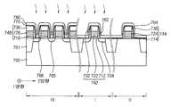
도 31 내지 도 37은 예시적인 실시예들에 따른 반도체 소자를 제조하는 방법을 설명하기 위한 단면도들이다. 상기 반도체 소자 제조 방법에서, 상보형 트랜지스터는 도 24 내지 도 28을 참조로 설명한 상보형 트랜지스터 형성 방법과 실질적으로 동일하거나 유사한 방법으로 형성되므로, 이에 대해서는 간략히 설명한다.31 to 37 are cross-sectional views illustrating a method of manufacturing a semiconductor device in accordance with example embodiments. In the method of fabricating the semiconductor device, since the complementary transistor is formed by substantially the same or similar method to the method of forming the complementary transistor described with reference to FIGS. 24 to 28, a brief description thereof will be provided.
도 31을 참조하면, 기판(700)에 소자 분리막(701)을 형성하고, 기판(700)의 제1 영역(I), 제2 영역(II) 및 제3 영역(III) 상에 제1 게이트 구조물(742), 제2 게이트 구조물(744) 및 제3 게이트 구조물(746)을 각각 형성한다. 각 게이트 구조물들(742, 744, 746)은 제1 방향으로 연장되며, 상기 제1 방향과 실질적으로 수직한 제2 방향을 따라 복수 개로 형성될 수 있다. 제3 영역(III)은 셀 영역일 수 있고, 제1 영역(I)은 주변 회로 영역의 NMOS 영역일 수 있으며, 제2 영역(II)은 주변 회로 영역의 PMOS 영역일 수 있다.Referring to FIG. 31, an
제1 내지 제3 게이트 구조물들(742, 744, 746)은 기판(700) 상에 게이트 절연막, 게이트 도전막 및 게이트 마스크 층을 순차적으로 형성한 후, 사진 식각 공정을 이용하여 이들을 패터닝 함으로써 형성할 수 있다. 이에 따라, 제1 게이트 구조물(742)은 기판(700)의 제1 영역(I) 상에 순차적으로 적층된 제1 게이트 절연막 패턴(712), 제1 게이트 전극(722) 및 제1 게이트 마스크(732)를 포함하도록 형성되고, 제2 게이트 구조물(744)은 기판(700)의 제2 영역(II) 상에 순차적으로 적층된 제2 게이트 절연막 패턴(714), 제2 게이트 전극(724) 및 제2 게이트 마스크(734)를 포함하도록 형성되며, 제3 게이트 구조물(746)은 기판(700)의 제3 영역(II) 상에 순차적으로 적층된 제3 게이트 절연막 패턴(716), 제3 게이트 전극(726) 및 제3 게이트 마스크(736)를 포함하도록 형성된다.The first to
도 32를 참조하면, 제2 게이트 구조물(744)을 커버하는 제1 마스크(751)를 기판(500)의 제2 영역(II) 상에 형성하고, 제1 및 제3 게이트 구조물들(742, 746)을 이온 주입 마스크로 사용하여 기판(700)의 제1 및 제3 영역들(I, III) 상부에 이온을 주입함으로써, 제1 및 제3 게이트 구조물들(742, 746)에 인접한 기판(700) 상부에 각각 제1 비정질 이온 주입 영역(702) 및 제2 비정질 이온 주입 영역(703)을 형성한다.Referring to FIG. 32, a
한편, 제1 및 제3 게이트 구조물들(742, 746)을 이온 주입 마스크로 사용하여 기판(700)의 제1 및 제3 영역(I, III) 상부에 제2 불순물을 주입함으로써, 제1 및 제3 게이트 구조물들(742, 746)에 인접한 기판(700) 상부에 각각 제2 및 제5 불순물 영역들(도시하지 않음)을 더 형성할 수도 있다. 상기 제2 불순물은 인, 비소 등과 같은 n형 불순물일 수 있다.Meanwhile, by using the first and
이후, 제1 마스크(751)는 제거된다.Thereafter, the
도 33을 참조하면, 제1 내지 제3 게이트 구조물들(742, 744, 746)의 측벽 상에 제1 스페이서(762), 제2 스페이서(764) 및 제3 스페이서(766)를 각각 형성한다. 구체적으로, 제1 내지 제3 게이트 구조물들(742, 744, 746)을 커버하는 스페이서 막을 형성한 후, 상기 스페이서 막을 이방성 식각 공정을 통해 부분적으로 제거함으로써 제1 내지 제3 스페이서들(762, 764, 766)을 형성할 수 있다.Referring to FIG. 33,
이후, 기판(700) 상에 제1 인장 스트레스 막(770) 및 제2 인장 스트레스 막(780)을 순차적으로 형성한다. 예시적인 실시예들에 따르면, 제1 및 제2 인장 스트레스 막들(770, 780)은 제1 내지 제3 게이트 구조물들(742, 744, 746) 및 제1 내지 제3 스페이서들(762, 764, 766)을 커버하도록 기판(700) 상에 형성될 수 있다. 제1 인장 스트레스 막(770)은 알루미늄 산화물(Al2O3), 금속 실리케이트 혹은 금속 실리콘 산질화물을 사용하여 형성될 수 있으며, 제2 인장 스트레스 막(780)은 실리콘 질화물을 사용하여 형성될 수 있다.Thereafter, the first
제1 및 제2 인장 스트레스 막들(770, 780)이 형성된 기판(700)을 열처리하여, 제1 및 제2 비정질 이온 주입 영역들(702, 703)을 재결정화시켜 각각 제1 및 제2 결정질 이온 주입 영역들(704, 705)을 형성한다. 예시적인 실시예들에 따르면, 상기 열처리는 제1 인장 스트레스 막(770)의 결정화 온도보다 낮은 온도에서 수행될 수 있다.The
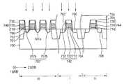
도 34를 참조하면, 제1 및 제2 인장 스트레스 막들(770, 780)을 제거한다. 제2 인장 스트레스 막(780)은 인산(H2PO3)을 포함하는 식각액을 사용하여 제거될 수 있고, 제1 인장 스트레스 막(770)은 불화수소(HF)를 포함하는 식각액을 사용하여 제거될 수 있다.Referring to FIG. 34, the first and second
제1 내지 제3 게이트 구조물들(742, 744, 746) 및 제1 내지 제3 스페이서들(762, 764, 766)을 커버하는 성장 방지막(757)을 형성한다. 예시적인 실시예들에 따르면, 성장 방지막(757)은 실리콘 산화물 혹은 실리콘 질화물을 사용하여 형성될 수 있다. 이후, 제1 및 제3 영역들(I, III) 상의 성장 방지막(757) 부분을 커버하는 제2 마스크(753)를 기판(700)의 제1 및 제3 영역들(I, III) 상에 형성한다. 제2 마스크(753)를 식각 마스크로 사용하여 제2 영역(II) 상의 성장 방지막(757) 부분을 제거한다.A
제2 마스크(753), 제2 게이트 구조물(744) 및 제2 스페이서(764)를 식각 마스크로 사용하여 기판(700)의 제2 영역(II) 상부를 식각한다. 이에 따라, 제2 게이트 구조물(744)에 인접한 기판(700) 상부에 트렌치(도시하지 않음)가 형성된다.An upper portion of the second region II of the
제2 마스크(753)를 제거한 후, 상기 트렌치를 채우는 제5 인장 스트레스 막(708)을 형성한다. 예시적인 실시예들에 따르면, 디클로로실란(SiH2Cl2) 가스 및 사수소화 게르마늄(GeH4) 가스 등을 소스 가스로 사용하여 SEG 공정을 수행함으로써, 상기 트렌치를 채우는 단결정 실리콘-게르마늄(SiGe) 층을 형성한다. 이때, 디보란(B2H6) 가스 등의 p형 불순물 소스 가스를 사용하여 상기 단결정 SiGe 층이 불순물을 포함하도록 할 수 있다. 이에 따라, 제5 인장 스트레스 막(708)은 제3 불순물 영역을 정의할 수 있다.After removing the
이후, 성장 방지막(757)은 제거된다.Thereafter, the
도 35를 참조하면, 제2 게이트 구조물(744)을 커버하는 제3 마스크(755)를 기판(700)의 제2 영역(II) 상에 형성한다. 제1 및 제3 게이트 구조물들(742, 746) 및 제1 및 제3 스페이서들(762, 766)을 이온 주입 마스크로 사용하여 기판(700)의 제1 및 제3 영역들(I, III) 상부에 제1 불순물을 주입함으로써 제1 및 제3 게이트 구조물들(742, 746)에 인접한 기판(700) 상부에 각각 제1 및 제4 불순물 영역들(706, 707)을 형성한다. 제4 불순물 영역(707)은 제1 소스/드레인 영역(707a) 및 제2 소스/드레인 영역(707b)을 포함할 수 있다. 상기 제1 불순물은 인 혹은 비소와 같은 n형 불순물을 포함할 수 있다.Referring to FIG. 35, a
이후 제3 마스크(755)는 제거된다.Thereafter, the
도 36을 참조하면, 게이트 구조물들(742, 744, 746) 및 스페이서들(762, 764, 766)을 커버하는 제1 층간 절연막(820)을 기판(700) 상에 형성한다. 제1 층간 절연막(820)은 비피에스지(Boro-phosphor Silicate Glass; BPSG), 유에스지(Undoped Silicate Glass; USG) 및 에스오지(Spin On Glass; SOG) 등과 같은 산화물을 사용하여 형성될 수 있다.Referring to FIG. 36, a first
제1 층간 절연막(820)을 관통하는 제1 개구들(도시하지 않음)을 형성하여 제1 및 제2 소스/드레인 영역들(707a, 707b)을 노출시키고, 상기 개구들을 채우는 제1 도전막을 기판(700) 및 제1 층간 절연막(820) 상에 형성한다. 상기 제1 도전막은 도핑된 폴리실리콘, 금속, 금속 질화물 및/또는 금속 실리사이드 등을 사용하여 형성될 수 있다. 제1 층간 절연막(820)의 상면이 노출될 때까지 상기 제1 도전막 상부를 평탄화하여, 제1 및 제2 소스/드레인 영역들(707a, 707b)에 각각 전기적으로 연결되는 제1 및 제2 플러그들(832, 834)을 형성한다.First openings (not shown) are formed through the first
제1 층간 절연막(820) 및 제1 및 제2 플러그들(832, 834) 상에 제2 층간 절연막(840)을 형성하고, 제2 층간 절연막을 관통하는 제2 개구들(도시하지 않음)을 형성하여, 제1 플러그(832) 및 제1 및 제3 불순물 영역들(706, 708)을 노출시킨다. 상기 제2 개구들을 채우는 제2 도전막을 기판(700), 제1 플러그(832) 및 제2 층간 절연막(840) 상에 형성한다. 상기 제2 도전막은 도핑된 폴리실리콘, 금속, 금속 질화물 및/또는 금속 실리사이드 등을 사용하여 형성될 수 있다. 제2 층간 절연막(840)의 상면이 노출될 때까지 상기 제2 도전막 상부를 평탄화하여, 제1 플러그(832)에 전기적으로 연결되는 비트 라인 콘택(850)을 형성하고, 제1 및 제3 불순물 영역들(706, 708)에 각각 전기적으로 연결되는 제3 및 제4 플러그들(862, 864)을 형성한다.A second
이후, 비트 라인 콘택(850) 및 제3 및 제4 플러그들(862, 864)에 접촉하는 제3 도전막을 제2 층간 절연막(840) 상에 형성하고 패터닝 하여, 비트 라인 콘택(850)에 전기적으로 연결되는 비트 라인(870) 및 제3 및 제4 플러그들(862, 864)에 각각 전기적으로 연결되는 제1 및 제2 배선들(882, 884)을 형성한다. 예시적인 실시예들에 따르면, 비트 라인(870)은 상기 제2 방향으로 연장되도록 형성될 수 있다. 상기 제3 도전막은 도핑된 폴리실리콘, 금속, 금속 질화물 및/또는 금속 실리사이드 등을 사용하여 형성될 수 있다.Thereafter, a third conductive layer contacting the
비트 라인(870) 및 제1 및 제2 배선들(882, 884)을 커버하는 제3 층간 절연막(900)을 제2 층간 절연막(840) 상에 형성한다.A third
도 37을 참조하면, 제2 및 제3 층간 절연막들(840, 900)을 관통하는 제3 개구들(도시하지 않음)을 형성하여 제2 플러그들(834)을 노출시킨다. 상기 제3 개구들을 채우는 제4 도전막을 제2 플러그들(834) 및 제3 층간 절연막(900) 상에 형성한다. 상기 제4 도전막은 도핑된 폴리실리콘, 금속, 금속 질화물 및/또는 금속 실리사이드 등을 사용하여 형성될 수 있다. 제3 층간 절연막(900)의 상면이 노출될 때까지 상기 제4 도전막 상부를 평탄화하여, 제2 플러그들(834)에 전기적으로 연결되는 커패시터 콘택들(910)을 형성한다.Referring to FIG. 37, third openings (not shown) through the second and third
커패시터 콘택들(910) 및 제3 층간 절연막(900) 상에 식각 저지막(920) 및 몰드막(도시하지 않음)을 형성한다. 예시적인 실시예들에 따르면, 식각 저지막(920)은 실리콘 질화물을 사용하여 형성될 수 있고, 상기 몰드막 실리콘 산화물을 사용하여 형성될 수 있다. 상기 몰드막 및 식각 저지막(920)을 관통하는 제4 개구들(도시하지 않음)을 형성하여 커패시터 콘택들(910)을 노출시킨다. 상기 제4 개구들의 내벽 및 상기 몰드막 상에 제5 도전막을 형성하고, 상기 제4 개구들을 채우는 희생막(도시하지 않음)을 상기 제5 도전막 상에 형성한다. 상기 제5 도전막은 도핑된 폴리실리콘, 금속, 금속 질화물 및/또는 금속 실리사이드 등을 사용하여 형성될 수 있다. 상기 몰드막 상면이 노출될 때까지, 상기 희생막 및 제5 도전막 상부를 평탄화하고, 상기 희생막을 제거한다. 이에 따라, 상기 제4 개구들 내벽 상에 하부 전극(930)이 형성된다.An
하부 전극(930) 및 식각 저지막(920) 상에 유전막(940)을 형성한다. 유전막(940)은 실리콘 질화물 또는 실리콘 질화물보다 높은 유전 상수를 갖는 고유전율 물질, 예를 들어, 탄탈륨 산화물, 하프늄 산화물, 알루미늄 산화물, 지르코늄 산화물 등을 사용하여 형성할 수 있다.The
유전막(940) 상에 상부 전극(950)을 형성한다. 상부 전극(950)은 도핑된 폴리실리콘, 금속, 금속 질화물 및/또는 금속 실리사이드 등을 사용하여 형성될 수 있다.An
하부 전극(930), 유전막(940) 및 상부 전극(950)은 커패시터(960)를 형성할 수 있다.The lower electrode 930, the
커패시터(960)를 커버하는 제4 층간 절연막(970)을 제3 층간 절연막(900) 상에 형성한다. 제4 층간 절연막(970)을 관통하는 제5 개구들(도시하지 않음)을 형성하여 제1 및 제2 배선들(882, 884)을 노출시킨다. 상기 제5 개구들을 채우는 제6 도전막을 제1 및 제2 배선들(882, 884) 및 제4 층간 절연막(970) 상에 형성한다. 제4 층간 절연막(970) 상면이 노출될 때까지 상기 제6 도전막 상부를 평탄화하여, 제1 및 제2 배선들(882, 884)에 각각 전기적으로 연결되는 제5 및 제6 플러그들(982, 984)을 형성한다.A fourth
이후, 제5 및 제6 플러그들(982, 984)에 각각 전기적으로 연결되는 제3 및 제4 배선들(992, 994)을 형성하고, 제3 및 제4 배선들(992, 994)을 보호하는 보호막(도시하지 않음)을 더 형성하여, 상기 반도체 소자를 완성한다.Thereafter, third and
상기 반도체 소자는 우수한 구동 전류 특성을 갖는 상보형 트랜지스터를 구비하므로, 우수한 전기적 특성을 가질 수 있다.Since the semiconductor device includes a complementary transistor having excellent driving current characteristics, the semiconductor device may have excellent electrical characteristics.
100, 300, 500, 700 : 기판
102, 302, 502 : 비정질 이온 주입 영역
104, 304, 504 : 결정질 이온 주입 영역106, 306 : 제1 불순물 영역
108 : 에피택시얼 층109 : ESD 층
110, 312 : 게이트 절연막 패턴120, 322 : 게이트 전극
130, 332 : 게이트 마스크
140, 150 : 제1, 제2 게이트 구조물160, 360 : 스페이서
170, 370 : 제1 인장 스트레스 막
180, 380 : 제2 인장 스트레스 막
190, 390 : 제3 인장 스트레스 막200, 400 : 식각 저지막
210, 410 : 제4 인장 스트레스 막305 : 리세스
506 : 제1 불순물 영역508 : 제5 인장 스트레스 막
542, 544 : 제1, 제2 게이트 구조물
551, 553, 555 : 제1, 제2, 제3 마스크562, 564 : 제1, 제2 스페이서
570, 770 : 제1 인장 스트레스 막
580, 780 : 제2 인장 스트레스 막
590, 610 : 제3, 제4 인장 스트레스 막600 : 식각 저지막
701 : 소자 분리막
702, 703 : 제1, 제2 비정질 이온 주입 영역
704, 705 : 제1, 제2 결정질 이온 주입 영역
706, 707 : 제1, 제4 불순물 영역
742, 744, 746 : 제1, 제2, 제3 게이트 구조물
751, 753, 755 : 제1, 제2, 제3 마스크
762, 764, 766 : 제1, 제2, 제3 스페이서
820, 840, 900, 970 : 제1, 제2, 제3, 제4 층간 절연막
832, 834 : 제1, 제2 플러그850 : 비트 라인 콘택
862, 864 : 제3, 제4 플러그870 : 비트 라인
882, 884 : 제1, 제2 배선910 : 커패시터 콘택
960 : 커패시터982, 984 : 제5, 제6 플러그100, 300, 500, 700: Substrate
102, 302, 502: amorphous ion implantation region
104, 304, 504: crystalline
108: epitaxial layer 109: ESD layer
110, 312: gate insulating
130, 332: gate mask
140, 150: first and
170, 370: first tensile stress film
180, 380: second tensile stress film
190,390: Third tensile stress film 200,400: etch stop film
210, 410: fourth tensile stress film 305: recess
506: First Impurity Region 508: Fifth Tensile Stress Film
542 and 544: first and second gate structures
551, 553, 555: first, second and
570, 770: first tensile stress film
580, 780: second tensile stress film
590, 610: third and fourth tensile stress film 600: etch stop film
701: device separator
702 and 703: first and second amorphous ion implantation regions
704, 705: first and second crystalline ion implantation region
706 and 707: first and fourth impurity regions
742, 744, 746: first, second, third gate structures
751, 753, 755: first, second, third mask
762, 764, 766: first, second, third spacer
820, 840, 900, 970: first, second, third, fourth interlayer insulating film
832 and 834: first and second plugs 850: bit line contacts
862, 864: third and fourth plug 870: bit line
882, 884: first and second wiring 910: capacitor contact
960:
Claims (30)
Translated fromKorean상기 게이트 구조물을 이온 주입 마스크로 사용하여 상기 기판의 상부에 비정질 이온 주입 영역을 형성하는 단계;
상기 게이트 구조물을 커버하도록 상기 기판 상에 금속 산화물을 포함하는 제1 인장 스트레스 막을 형성하는 단계;
상기 기판을 열처리하여 상기 비정질 이온 주입 영역을 결정화하는 단계;
상기 제1 인장 스트레스 막을 제거하는 단계; 및
상기 게이트 구조물을 이온 주입 마스크로 사용하여 상기 기판의 상부에 제1 불순물을 도핑하는 단계를 포함하는 트랜지스터 형성 방법.Forming a gate structure on the substrate;
Forming an amorphous ion implantation region on the substrate using the gate structure as an ion implantation mask;
Forming a first tensile stress film comprising a metal oxide on the substrate to cover the gate structure;
Heat treating the substrate to crystallize the amorphous ion implanted region;
Removing the first tensile stress film; And
Doping a first impurity on the substrate using the gate structure as an ion implantation mask.
상기 열처리 단계 이후에, 상기 제2 인장 스트레스 막을 제거하는 단계를 더 포함하는 것을 특징으로 하는 트랜지스터 형성 방법.The method of claim 1, further comprising forming a second tensile stress film comprising silicon nitride on the first tensile stress film between the forming of the first tensile stress film and the heat treatment step.
After the heat treatment step, further comprising the step of removing the second tensile stress film.
상기 열처리 단계 이후에, 상기 식각 방지막을 제거하는 단계를 더 포함하는 것을 특징으로 하는 트랜지스터 형성 방법.The method of claim 1, further comprising forming an etch stop layer including silicon oxide on the substrate prior to forming the first tensile stress film.
And removing the etch stop layer after the heat treatment step.
상기 게이트 구조물 측벽 상에 질화물을 포함하는 스페이서를 형성하는 단계를 더 포함하는 것을 특징으로 하는 트랜지스터 형성 방법.The method of claim 1, wherein after forming the amorphous ion implantation region,
And forming a spacer on the sidewall of the gate structure, the spacer comprising nitride.
상기 게이트 구조물 및 상기 스페이서를 이온 주입 마스크로 사용하여 수행되는 것을 특징으로 하는 트랜지스터 형성 방법.The method of claim 17, wherein the doping the first impurity comprises:
And using the gate structure and the spacer as an ion implantation mask.
상기 기판 상부에 리세스를 형성하는 단계;
상기 리세스 내벽에 게이트 절연막 패턴을 형성하는 단계; 및
상기 리세스 내부를 채우는 게이트 전극을 상기 게이트 절연막 패턴 상에 형성하는 단계를 포함하는 것을 특징으로 하는 트랜지스터 형성 방법.The method of claim 1, wherein the forming of the gate structure comprises:
Forming a recess on the substrate;
Forming a gate insulating layer pattern on the inner wall of the recess; And
And forming a gate electrode filling the recesses on the gate insulating layer pattern.
상기 결정질 이온 주입 영역 상에 에피택시얼 층을 형성하는 단계를 더 포함하고,
상기 제1 불순물을 도핑하는 단계는 상기 에피택시얼 층에 상기 제1 불순물을 도핑하는 단계를 포함하는 것을 특징으로 하는 트랜지스터 형성 방법.The method of claim 1, wherein after removing the first tensile stress film,
Forming an epitaxial layer on the crystalline ion implantation region,
Doping the first impurity comprises doping the epitaxial layer with the first impurity.
상기 제1 게이트 구조물을 이온 주입 마스크로 사용하여 상기 기판의 제1 영역 상부에 비정질 이온 주입 영역을 형성하는 단계;
상기 제1 및 제2 게이트 구조물들을 커버하도록 상기 기판 상에 금속 산화물을 포함하는 제1 인장 스트레스 막을 형성하는 단계;
상기 기판을 열처리하여 상기 비정질 이온 주입 영역을 결정화하는 단계;
상기 제1 인장 스트레스 막을 제거하는 단계;
상기 제2 게이트 구조물에 인접한 상기 기판의 제2 영역 상부에 제2 인장 스트레스 막을 형성하는 단계; 및
상기 제1 게이트 구조물을 이온 주입 마스크로 사용하여 상기 기판의 제1 영역 상부에 제1 불순물 영역을 형성하는 단계를 포함하는 상보형 트랜지스터 형성 방법.Forming first and second gate structures on first and second regions of the substrate, respectively;
Forming an amorphous ion implantation region over the first region of the substrate using the first gate structure as an ion implantation mask;
Forming a first tensile stress film comprising a metal oxide on the substrate to cover the first and second gate structures;
Heat treating the substrate to crystallize the amorphous ion implanted region;
Removing the first tensile stress film;
Forming a second tensile stress film over the second region of the substrate adjacent the second gate structure; And
Forming a first impurity region over the first region of the substrate using the first gate structure as an ion implantation mask.
상기 제2 인장 스트레스 막은 p형 불순물을 포함하는 실리콘-게르마늄 층으로서 제2 불순물 영역을 형성하는 것을 특징으로 하는 상보형 트랜지스터 형성 방법.The method of claim 21, wherein the substrate comprises silicon,
And the second tensile stress film forms a second impurity region as a silicon-germanium layer containing a p-type impurity.
상기 제2 게이트 구조물에 인접한 상기 기판의 제2 영역 상부에 트렌치를 형성하는 단계; 및
에피택시얼 성장 공정을 통해 상기 트렌치를 채우는 상기 p형 불순물을 포함하는 실리콘-게르마늄 층을 형성하는 단계를 포함하는 것을 특징으로 하는 상보형 트랜지스터 형성 방법.The method of claim 23, wherein forming a silicon-germanium layer including the p-type impurity comprises:
Forming a trench over the second region of the substrate adjacent the second gate structure; And
Forming a silicon-germanium layer comprising the p-type impurity filling the trench through an epitaxial growth process.
상기 제1 및 제3 게이트 구조물들을 이온 주입 마스크로 사용하여 상기 기판의 제1 및 제3 영역들 상부에 비정질 이온 주입 영역을 형성하는 단계;
상기 제1 내지 제3 게이트 구조물들을 커버하도록 상기 기판 상에 금속 산화물을 포함하는 제1 인장 스트레스 막을 형성하는 단계;
상기 기판을 열처리하여 상기 비정질 이온 주입 영역을 결정화하는 단계;
상기 제1 인장 스트레스 막을 제거하는 단계;
상기 제2 게이트 구조물에 인접한 상기 기판의 제2 영역 상부에 제2 인장 스트레스 막을 형성하는 단계;
상기 제1 및 제3 게이트 구조물들을 이온 주입 마스크로 사용하여 상기 기판의 제1 및 제3 영역들 상부에 각각 제1 및 제3 불순물 영역들을 형성하는 단계; 및
상기 제3 불순물 영역 일부에 전기적으로 연결되는 커패시터를 형성하는 단계를 포함하는 반도체 소자 제조 방법.Forming first to third gate structures on first to third regions of the substrate, respectively;
Forming an amorphous ion implantation region over the first and third regions of the substrate using the first and third gate structures as an ion implantation mask;
Forming a first tensile stress film comprising a metal oxide on the substrate to cover the first to third gate structures;
Heat treating the substrate to crystallize the amorphous ion implanted region;
Removing the first tensile stress film;
Forming a second tensile stress film over the second region of the substrate adjacent the second gate structure;
Forming first and third impurity regions on the first and third regions of the substrate, respectively, using the first and third gate structures as ion implantation masks; And
Forming a capacitor electrically connected to a portion of the third impurity region.
Priority Applications (2)
| Application Number | Priority Date | Filing Date | Title |
|---|---|---|---|
| KR1020100086415AKR20120023968A (en) | 2010-09-03 | 2010-09-03 | Methods of forming transistors, methods of forming cmos transistors and methods of manufacturing semiconductor devices using the same |
| US12/944,774US8101480B1 (en) | 2010-09-03 | 2010-11-12 | Methods of forming transistors and CMOS semiconductor devices using an SMT technique |
Applications Claiming Priority (1)
| Application Number | Priority Date | Filing Date | Title |
|---|---|---|---|
| KR1020100086415AKR20120023968A (en) | 2010-09-03 | 2010-09-03 | Methods of forming transistors, methods of forming cmos transistors and methods of manufacturing semiconductor devices using the same |
Publications (1)
| Publication Number | Publication Date |
|---|---|
| KR20120023968Atrue KR20120023968A (en) | 2012-03-14 |
Family
ID=45476798
Family Applications (1)
| Application Number | Title | Priority Date | Filing Date |
|---|---|---|---|
| KR1020100086415AAbandonedKR20120023968A (en) | 2010-09-03 | 2010-09-03 | Methods of forming transistors, methods of forming cmos transistors and methods of manufacturing semiconductor devices using the same |
Country Status (2)
| Country | Link |
|---|---|
| US (1) | US8101480B1 (en) |
| KR (1) | KR20120023968A (en) |
Cited By (1)
| Publication number | Priority date | Publication date | Assignee | Title |
|---|---|---|---|---|
| CN107968035A (en)* | 2016-10-19 | 2018-04-27 | 株式会社村田制作所 | Semiconductor device and its manufacture method |
Families Citing this family (22)
| Publication number | Priority date | Publication date | Assignee | Title |
|---|---|---|---|---|
| US7860803B1 (en)* | 2006-02-15 | 2010-12-28 | Google Inc. | Method and system for obtaining feedback for a product |
| US9202913B2 (en)* | 2010-09-30 | 2015-12-01 | Institute of Microelectronics, Chinese Academy of Sciences | Method for manufacturing semiconductor structure |
| US9105379B2 (en) | 2011-01-21 | 2015-08-11 | Uchicago Argonne, Llc | Tunable resistance coatings |
| US8969823B2 (en)* | 2011-01-21 | 2015-03-03 | Uchicago Argonne, Llc | Microchannel plate detector and methods for their fabrication |
| US8921799B2 (en) | 2011-01-21 | 2014-12-30 | Uchicago Argonne, Llc | Tunable resistance coatings |
| US9184052B2 (en)* | 2012-10-25 | 2015-11-10 | Samsung Electronics Co., Ltd. | Semiconductor device and manufacturing method of semiconductor device using metal oxide |
| US11326255B2 (en) | 2013-02-07 | 2022-05-10 | Uchicago Argonne, Llc | ALD reactor for coating porous substrates |
| US9224607B2 (en)* | 2013-09-18 | 2015-12-29 | Globalfoundries Inc. | Dual epitaxy region integration |
| US9762443B2 (en) | 2014-04-15 | 2017-09-12 | Splunk Inc. | Transformation of network data at remote capture agents |
| US10127273B2 (en) | 2014-04-15 | 2018-11-13 | Splunk Inc. | Distributed processing of network data using remote capture agents |
| US10462004B2 (en) | 2014-04-15 | 2019-10-29 | Splunk Inc. | Visualizations of statistics associated with captured network data |
| US12028208B1 (en) | 2014-05-09 | 2024-07-02 | Splunk Inc. | Selective event stream data storage based on network traffic volume |
| US10523521B2 (en) | 2014-04-15 | 2019-12-31 | Splunk Inc. | Managing ephemeral event streams generated from captured network data |
| JP2016051740A (en)* | 2014-08-28 | 2016-04-11 | ルネサスエレクトロニクス株式会社 | Method of manufacturing semiconductor device |
| KR102274765B1 (en) | 2014-12-17 | 2021-07-09 | 에스케이하이닉스 주식회사 | Electronic device and method for fabricating the sam |
| US9704881B2 (en)* | 2015-09-21 | 2017-07-11 | Globalfoundries Inc. | Semiconductor device with reduced poly spacing effect |
| US10043903B2 (en) | 2015-12-21 | 2018-08-07 | Samsung Electronics Co., Ltd. | Semiconductor devices with source/drain stress liner |
| KR102414957B1 (en) | 2018-06-15 | 2022-06-29 | 삼성전자주식회사 | Method for fabricating semiconductor device |
| US11111578B1 (en) | 2020-02-13 | 2021-09-07 | Uchicago Argonne, Llc | Atomic layer deposition of fluoride thin films |
| US12065738B2 (en) | 2021-10-22 | 2024-08-20 | Uchicago Argonne, Llc | Method of making thin films of sodium fluorides and their derivatives by ALD |
| US11901169B2 (en) | 2022-02-14 | 2024-02-13 | Uchicago Argonne, Llc | Barrier coatings |
| CN115547936B (en)* | 2022-12-02 | 2023-06-16 | 合肥晶合集成电路股份有限公司 | Method for manufacturing semiconductor structure |
Family Cites Families (6)
| Publication number | Priority date | Publication date | Assignee | Title |
|---|---|---|---|---|
| US7772062B2 (en)* | 2005-02-08 | 2010-08-10 | Taiwan Semiconductor Manufacturing Co., Ltd. | MOSFET having a channel mechanically stressed by an epitaxially grown, high k strain layer |
| US7785950B2 (en) | 2005-11-10 | 2010-08-31 | International Business Machines Corporation | Dual stress memory technique method and related structure |
| US20070141775A1 (en)* | 2005-12-15 | 2007-06-21 | Chartered Semiconductor Manufacturing, Ltd. | Modulation of stress in stress film through ion implantation and its application in stress memorization technique |
| US7678636B2 (en) | 2006-06-29 | 2010-03-16 | Taiwan Semiconductor Manufacturing Company, Ltd. | Selective formation of stress memorization layer |
| US7834399B2 (en) | 2007-06-05 | 2010-11-16 | International Business Machines Corporation | Dual stress memorization technique for CMOS application |
| KR100844933B1 (en)* | 2007-06-26 | 2008-07-09 | 주식회사 하이닉스반도체 | Transistor of semiconductor device and manufacturing method thereof |
- 2010
- 2010-09-03KRKR1020100086415Apatent/KR20120023968A/ennot_activeAbandoned
- 2010-11-12USUS12/944,774patent/US8101480B1/enactiveActive
Cited By (2)
| Publication number | Priority date | Publication date | Assignee | Title |
|---|---|---|---|---|
| CN107968035A (en)* | 2016-10-19 | 2018-04-27 | 株式会社村田制作所 | Semiconductor device and its manufacture method |
| CN107968035B (en)* | 2016-10-19 | 2022-02-25 | 株式会社村田制作所 | Semiconductor device and method for manufacturing the same |
Also Published As
| Publication number | Publication date |
|---|---|
| US8101480B1 (en) | 2012-01-24 |
Similar Documents
| Publication | Publication Date | Title |
|---|---|---|
| KR20120023968A (en) | Methods of forming transistors, methods of forming cmos transistors and methods of manufacturing semiconductor devices using the same | |
| US8835936B2 (en) | Source and drain doping using doped raised source and drain regions | |
| JP6275559B2 (en) | Semiconductor device and manufacturing method thereof | |
| US20180374926A1 (en) | Semiconductor device and method of manufacturing the same | |
| KR101511413B1 (en) | Contact structure of semiconductor device | |
| CN1945854B (en) | Strained semiconductor device and method of making the same | |
| US8409947B2 (en) | Method of manufacturing semiconductor device having stress creating layer | |
| US10644158B2 (en) | Semiconductor device including fin field effect transistor and method of manufacturing the same | |
| KR20120012705A (en) | Semiconductor device and manufacturing method thereof | |
| US8710549B2 (en) | MOS device for eliminating floating body effects and self-heating effects | |
| KR101721036B1 (en) | Semiconductor devices and methods of manufacturing the same | |
| US20120132986A1 (en) | Semiconductor devices and methods of manufacturing the same | |
| US10199392B2 (en) | FinFET device having a partially dielectric isolated fin structure | |
| US20150162433A1 (en) | Method for the formation of a finfet device with epitaxially grown source-drain regions having a reduced leakage path | |
| KR101197464B1 (en) | Method of manufacturing a semiconductor device | |
| KR20150047218A (en) | Semiconductor devices and methods of manufacturing the same | |
| JP2011009412A (en) | Semiconductor device, and method of fabricating the same | |
| KR20150068084A (en) | Semiconductor devices and methods of manufacturing the same | |
| KR20140121617A (en) | Semiconductor devices and methods of manufacturing the same | |
| US20150235906A1 (en) | Methods for etching dielectric materials in the fabrication of integrated circuits | |
| US20090085075A1 (en) | Method of fabricating mos transistor and mos transistor fabricated thereby | |
| KR102449608B1 (en) | Method for manufacturing semiconductor device | |
| JP2011238780A (en) | Semiconductor device and method of manufacturing the same | |
| CN110718548B (en) | Semiconductor Devices | |
| EP4243063A2 (en) | Semiconductor device and method of fabricating the same |
Legal Events
| Date | Code | Title | Description |
|---|---|---|---|
| PA0109 | Patent application | Patent event code:PA01091R01D Comment text:Patent Application Patent event date:20100903 | |
| PG1501 | Laying open of application | ||
| A201 | Request for examination | ||
| PA0201 | Request for examination | Patent event code:PA02012R01D Patent event date:20150810 Comment text:Request for Examination of Application Patent event code:PA02011R01I Patent event date:20100903 Comment text:Patent Application | |
| E902 | Notification of reason for refusal | ||
| PE0902 | Notice of grounds for rejection | Comment text:Notification of reason for refusal Patent event date:20161128 Patent event code:PE09021S01D | |
| E701 | Decision to grant or registration of patent right | ||
| PE0701 | Decision of registration | Patent event code:PE07011S01D Comment text:Decision to Grant Registration Patent event date:20170322 | |
| PC1904 | Unpaid initial registration fee |