KR20120022601A - Semiconductor device - Google Patents
Semiconductor deviceDownload PDFInfo
- Publication number
- KR20120022601A KR20120022601AKR1020110077303AKR20110077303AKR20120022601AKR 20120022601 AKR20120022601 AKR 20120022601AKR 1020110077303 AKR1020110077303 AKR 1020110077303AKR 20110077303 AKR20110077303 AKR 20110077303AKR 20120022601 AKR20120022601 AKR 20120022601A
- Authority
- KR
- South Korea
- Prior art keywords
- transistor
- electrode
- oxide semiconductor
- insulating layer
- oxide
- Prior art date
- Legal status (The legal status is an assumption and is not a legal conclusion. Google has not performed a legal analysis and makes no representation as to the accuracy of the status listed.)
- Granted
Links
Images


Classifications
- G—PHYSICS
- G11—INFORMATION STORAGE
- G11C—STATIC STORES
- G11C11/00—Digital stores characterised by the use of particular electric or magnetic storage elements; Storage elements therefor
- G11C11/21—Digital stores characterised by the use of particular electric or magnetic storage elements; Storage elements therefor using electric elements
- G11C11/34—Digital stores characterised by the use of particular electric or magnetic storage elements; Storage elements therefor using electric elements using semiconductor devices
- G11C11/40—Digital stores characterised by the use of particular electric or magnetic storage elements; Storage elements therefor using electric elements using semiconductor devices using transistors
- G11C11/401—Digital stores characterised by the use of particular electric or magnetic storage elements; Storage elements therefor using electric elements using semiconductor devices using transistors forming cells needing refreshing or charge regeneration, i.e. dynamic cells
- G11C11/403—Digital stores characterised by the use of particular electric or magnetic storage elements; Storage elements therefor using electric elements using semiconductor devices using transistors forming cells needing refreshing or charge regeneration, i.e. dynamic cells with charge regeneration common to a multiplicity of memory cells, i.e. external refresh
- G—PHYSICS
- G11—INFORMATION STORAGE
- G11C—STATIC STORES
- G11C16/00—Erasable programmable read-only memories
- G11C16/02—Erasable programmable read-only memories electrically programmable
- G11C16/04—Erasable programmable read-only memories electrically programmable using variable threshold transistors, e.g. FAMOS
- G11C16/0408—Erasable programmable read-only memories electrically programmable using variable threshold transistors, e.g. FAMOS comprising cells containing floating gate transistors
- G11C16/0433—Erasable programmable read-only memories electrically programmable using variable threshold transistors, e.g. FAMOS comprising cells containing floating gate transistors comprising cells containing a single floating gate transistor and one or more separate select transistors
- G—PHYSICS
- G11—INFORMATION STORAGE
- G11C—STATIC STORES
- G11C16/00—Erasable programmable read-only memories
- G11C16/02—Erasable programmable read-only memories electrically programmable
- G11C16/04—Erasable programmable read-only memories electrically programmable using variable threshold transistors, e.g. FAMOS
- G11C16/0483—Erasable programmable read-only memories electrically programmable using variable threshold transistors, e.g. FAMOS comprising cells having several storage transistors connected in series
- H—ELECTRICITY
- H10—SEMICONDUCTOR DEVICES; ELECTRIC SOLID-STATE DEVICES NOT OTHERWISE PROVIDED FOR
- H10B—ELECTRONIC MEMORY DEVICES
- H10B41/00—Electrically erasable-and-programmable ROM [EEPROM] devices comprising floating gates
- H—ELECTRICITY
- H10—SEMICONDUCTOR DEVICES; ELECTRIC SOLID-STATE DEVICES NOT OTHERWISE PROVIDED FOR
- H10B—ELECTRONIC MEMORY DEVICES
- H10B41/00—Electrically erasable-and-programmable ROM [EEPROM] devices comprising floating gates
- H10B41/70—Electrically erasable-and-programmable ROM [EEPROM] devices comprising floating gates the floating gate being an electrode shared by two or more components
- H—ELECTRICITY
- H10—SEMICONDUCTOR DEVICES; ELECTRIC SOLID-STATE DEVICES NOT OTHERWISE PROVIDED FOR
- H10B—ELECTRONIC MEMORY DEVICES
- H10B63/00—Resistance change memory devices, e.g. resistive RAM [ReRAM] devices
- H10B63/80—Arrangements comprising multiple bistable or multi-stable switching components of the same type on a plane parallel to the substrate, e.g. cross-point arrays
- H—ELECTRICITY
- H10—SEMICONDUCTOR DEVICES; ELECTRIC SOLID-STATE DEVICES NOT OTHERWISE PROVIDED FOR
- H10D—INORGANIC ELECTRIC SEMICONDUCTOR DEVICES
- H10D30/00—Field-effect transistors [FET]
- H10D30/60—Insulated-gate field-effect transistors [IGFET]
- H10D30/67—Thin-film transistors [TFT]
- H10D30/6729—Thin-film transistors [TFT] characterised by the electrodes
- H10D30/673—Thin-film transistors [TFT] characterised by the electrodes characterised by the shapes, relative sizes or dispositions of the gate electrodes
- H10D30/6733—Multi-gate TFTs
- H—ELECTRICITY
- H10—SEMICONDUCTOR DEVICES; ELECTRIC SOLID-STATE DEVICES NOT OTHERWISE PROVIDED FOR
- H10D—INORGANIC ELECTRIC SEMICONDUCTOR DEVICES
- H10D86/00—Integrated devices formed in or on insulating or conducting substrates, e.g. formed in silicon-on-insulator [SOI] substrates or on stainless steel or glass substrates
- H10D86/40—Integrated devices formed in or on insulating or conducting substrates, e.g. formed in silicon-on-insulator [SOI] substrates or on stainless steel or glass substrates characterised by multiple TFTs
- H10D86/60—Integrated devices formed in or on insulating or conducting substrates, e.g. formed in silicon-on-insulator [SOI] substrates or on stainless steel or glass substrates characterised by multiple TFTs wherein the TFTs are in active matrices
- H—ELECTRICITY
- H10—SEMICONDUCTOR DEVICES; ELECTRIC SOLID-STATE DEVICES NOT OTHERWISE PROVIDED FOR
- H10D—INORGANIC ELECTRIC SEMICONDUCTOR DEVICES
- H10D86/00—Integrated devices formed in or on insulating or conducting substrates, e.g. formed in silicon-on-insulator [SOI] substrates or on stainless steel or glass substrates
- H10D86/40—Integrated devices formed in or on insulating or conducting substrates, e.g. formed in silicon-on-insulator [SOI] substrates or on stainless steel or glass substrates characterised by multiple TFTs
- H10D86/421—Integrated devices formed in or on insulating or conducting substrates, e.g. formed in silicon-on-insulator [SOI] substrates or on stainless steel or glass substrates characterised by multiple TFTs having a particular composition, shape or crystalline structure of the active layer
- H10D86/423—Integrated devices formed in or on insulating or conducting substrates, e.g. formed in silicon-on-insulator [SOI] substrates or on stainless steel or glass substrates characterised by multiple TFTs having a particular composition, shape or crystalline structure of the active layer comprising semiconductor materials not belonging to the Group IV, e.g. InGaZnO
Landscapes
- Engineering & Computer Science (AREA)
- Microelectronics & Electronic Packaging (AREA)
- Computer Hardware Design (AREA)
- Semiconductor Memories (AREA)
- Thin Film Transistor (AREA)
- Non-Volatile Memory (AREA)
- Dram (AREA)
- Metal-Oxide And Bipolar Metal-Oxide Semiconductor Integrated Circuits (AREA)
Abstract
Translated fromKoreanDescription
Translated fromKorean개시하는 발명은 반도체 소자를 이용한 반도체 장치에 관한 것이다.
The disclosed invention relates to a semiconductor device using a semiconductor element.
반도체 소자를 이용한 기억 장치는 전력이 공급되지 않으면 기억 내용이 소멸되는 휘발성 기억 장치와, 전력이 공급되지 않아도 기억 내용이 유지되는 비휘발성 기억 장치로 크게 나눌 수 있다.Memory devices using semiconductor devices can be broadly classified into volatile memory devices whose memory contents are lost when no power is supplied, and nonvolatile memory devices whose memory contents are maintained even when no power is supplied.
휘발성 기억 장치의 대표적인 예로서는, DRAM(Dynamic Random Access Memory)이 알려져 있다. DRAM은 기억 소자를 구성하는 트랜지스터를 선택하여 커패시터에 전하를 축적함으로써 정보를 기억한다.As a representative example of the volatile memory device, a DRAM (Dynamic Random Access Memory) is known. The DRAM stores information by selecting a transistor constituting the memory element and accumulating charge in the capacitor.
DRAM에서는 정보를 판독하면 커패시터의 전하가 소멸되기 때문에 정보를 판독할 때마다 다시 기록 동작을 행할 필요가 있다. 또한, 기억 소자를 구성하는 트랜지스터에서는 오프 상태에서 소스와 드레인 사이의 누설 전류(오프 전류) 등에 의하여 트랜지스터가 선택되지 않는 상황에서도 전하가 유출 또는 유입되기 때문에 데이터의 유지 기간이 짧다. 따라서, 소정의 주기에 다시 기록 동작(리프레시 동작)을 행할 필요가 있고, 소비 전력을 충분히 저감하기 어렵다. 또한, 전력이 공급되지 않으면 기억 내용이 소멸되기 때문에 오랜 기간에 걸쳐 기억을 유지하기 위해서는 자성 재료나 광학 재료를 이용한 다른 기억 장치가 필요하다.In DRAM, when the information is read out, the charge of the capacitor disappears, so it is necessary to perform the write operation again each time the information is read out. Further, in the transistors constituting the memory element, the data retention period is short because charges flow out or flow in the off state even when the transistor is not selected due to leakage current (off current) between the source and the drain. Therefore, it is necessary to perform a write operation (refresh operation) again at a predetermined cycle, and it is difficult to sufficiently reduce power consumption. In addition, since the contents of the memory disappear when the power is not supplied, another memory device using a magnetic material or an optical material is required to retain the memory for a long time.
휘발성 기억 장치의 다른 예로서는 SRAM(Static Random Access Memory)이 알려져 있다. SRAM은 플립플롭 등의 회로를 사용하여 기억 내용을 유지하기 때문에 리프레시 동작을 행할 필요가 없고, 이 점에서는 DRAM보다 유리하다. 그러나, 플립플롭 등의 회로를 사용하기 때문에 단위 면적당의 기억 용량이 작게 되는 문제가 있다. 또한, 전력이 공급되지 않으면 기억 내용이 소멸되는 점은 DRAM과 마찬가지다.Another example of a volatile memory device is a static random access memory (SRAM). Since the SRAM uses a circuit such as flip-flop to hold the contents of the memory, there is no need to perform the refresh operation, which is advantageous over the DRAM in this regard. However, there is a problem that the storage capacity per unit area becomes small because circuits such as flip-flops are used. In addition, similar to DRAM, the contents of the memory disappear when the power is not supplied.
비휘발성 기억 장치의 예로서 플래시 메모리가 알려져 있다. 플래시 메모리는 트랜지스터의 게이트 전극과 채널 형성 영역 사이에 부유 게이트를 갖고, 상기 부유 게이트에 전하를 유지시킴으로써 데이터를 기억하기 때문에 데이터의 유지 기간은 극히 오래 가고(반영구적), 휘발성 기억 장치에서 필요한 리프레시 동작을 행할 필요가 없는 이점을 갖는다(예를 들어, 특허문헌 1 참조).Flash memory is known as an example of a nonvolatile memory device. Since the flash memory has a floating gate between the gate electrode of the transistor and the channel formation region, and stores data by retaining charge in the floating gate, the data retention period is extremely long (semi-permanent), and the refresh operation required in the volatile memory device. It has the advantage that it is not necessary to carry out (for example, refer patent document 1).
그러나, 기록 동작시에 생기는 터널 전류로 인하여 기억 소자를 구성하는 게이트 절연층이 열화되기 때문에 소정 횟수 이상 기록 동작이 행해짐으로써 기억 소자가 기능하지 않게 되는 문제가 생긴다. 이 문제의 영향을 완화하기 위하여, 예를 들어, 각 기억 소자의 기록 횟수를 균일화하는 기법이 채용되지만, 이것을 실현하기 위해서는 복잡한 주변 회로가 필요하게 된다. 그리고, 이러한 기법을 채용하여도 근본적인 수명 문제가 해소되는 것은 아니다. 즉, 플래시 메모리는 정보를 재기록하는 빈도가 높은 용도에는 부적합하다.However, since the gate insulating layer constituting the memory element deteriorates due to the tunnel current generated during the write operation, a problem occurs that the memory element does not function by performing the write operation a predetermined number of times or more. In order to alleviate the influence of this problem, for example, a technique of equalizing the number of times of writing of each memory element is employed, but a complicated peripheral circuit is required to realize this. And even adopting these techniques does not solve the fundamental lifetime problem. In other words, the flash memory is unsuitable for a high frequency of rewriting information.
또한, 부유 게이트에 전하를 주입시키거나 또는 그 전하를 제거하기 위하여 높은 전압이 필요하고, 또한 높은 전압을 생성하기 위한 회로도 필요하다. 또한, 전하의 주입 또는 제거에는 비교적 오랜 시간이 걸리고, 기록이나 소거의 고속화가 용이하지 않은 문제도 있다.
In addition, a high voltage is required to inject charge into or remove the charge from the floating gate, and a circuit for generating a high voltage is also required. In addition, the injection or removal of electric charges takes a relatively long time, and there is also a problem in that writing and erasing are not easy.
상술한 문제를 감안하여 본 발명의 일 형태는 전력이 공급되지 않는 상황에서도 기억 내용을 유지할 수 있고, 또 배선 개수를 삭감함으로써 고집적화가 도모된 반도체 장치를 제공하는 것을 목적으로 한다.
In view of the above-mentioned problems, one embodiment of the present invention aims to provide a semiconductor device which can maintain the stored contents even in a situation where electric power is not supplied and by reducing the number of wirings, thereby achieving high integration.
개시하는 발명의 일 형태에서는 트랜지스터의 오프 전류를 충분히 작게 할 수 있는 재료, 예를 들어, 와이드 갭 반도체인 산화물 반도체 재료를 사용하여 반도체 장치를 구성한다. 트랜지스터의 오프 전류를 충분히 작게 할 수 있는 반도체 재료를 사용함으로써 오랜 기간에 걸쳐 정보를 유지할 수 있다.In one embodiment of the disclosed invention, a semiconductor device is formed by using a material capable of sufficiently reducing the off current of a transistor, for example, an oxide semiconductor material which is a wide gap semiconductor. By using a semiconductor material capable of sufficiently reducing the off current of the transistor, information can be retained over a long period of time.
본 명세서에서 개시하는 본 발명의 일 형태는 소스선과, n(n은 자연수)개의 비트선과, 소스선과 비트선 사이에 직렬로 접속된 제 1 메모리 셀 내지 제 m(m은 자연수) 메모리 셀과, m+1개의 워드선과, 제 1 선택선 및 제 2 선택선과, 게이트 전극이 제 1 선택선과 전기적으로 접속된 제 1 선택 트랜지스터와, 게이트 전극이 제 2 선택선과 전기적으로 접속된 제 2 선택 트랜지스터를 포함하고, 메모리 셀은 제 1 게이트 전극, 제 1 소스 전극, 및 제 1 드레인 전극을 포함하는 제 1 트랜지스터와, 제 2 게이트 전극, 제 2 소스 전극, 및 제 2 드레인 전극을 포함하는 제 2 트랜지스터와, 용량 소자를 포함하고, 제 1 트랜지스터는 반도체 재료를 함유한 기판에 제공되고, 제 2 트랜지스터는 산화물 반도체층을 포함하여 구성되고, 소스선은 제 2 선택 트랜지스터를 통하여 제 m 메모리 셀의 제 1 소스 전극과 전기적으로 접속되고, 비트선은 제 1 선택 트랜지스터를 통하여 제 1 메모리 셀의 제 1 드레인 전극과 전기적으로 접속되고 또 제 1 메모리 셀의 제 2 드레인 전극과 전기적으로 접속되고, 제 1 워드선은 제 1 메모리 셀의 제 2 게이트 전극과 전기적으로 접속되고, 제 k(k는 2 이상 m 이하의 자연수) 워드선은 제 k 메모리 셀의 제 2 게이트 전극과 전기적으로 접속되고 또 제 k-1 메모리 셀의 용량 소자의 전극의 한쪽과 전기적으로 접속되고, 제 k 메모리 셀의 제 1 드레인 전극은 제 k-1 메모리 셀의 제 1 소스 전극과 전기적으로 접속되고, 제 m 메모리 셀의 제 1 게이트 전극과 제 m 메모리 셀의 제 2 소스 전극과 제 m 메모리 셀의 용량 소자의 전극의 다른 쪽이 전기적으로 접속되는 것을 특징으로 하는 반도체 장치다.One embodiment of the present invention disclosed in this specification includes a source line, n (n is a natural number) bit lines, first to m-th memory cells (m is a natural number) connected in series between the source line and the bit line, a m + 1 word line, a first selection line and a second selection line, a first selection transistor in which the gate electrode is electrically connected to the first selection line, and a second selection transistor in which the gate electrode is electrically connected to the second selection line. The memory cell includes a first transistor including a first gate electrode, a first source electrode, and a first drain electrode, and a second transistor including a second gate electrode, a second source electrode, and a second drain electrode. And a capacitor, wherein the first transistor is provided on a substrate containing a semiconductor material, the second transistor comprises an oxide semiconductor layer, and the source line is connected to the mth through the second select transistor. Electrically connected to the first source electrode of the memory cell, the bit line being electrically connected to the first drain electrode of the first memory cell through the first select transistor and electrically connected to the second drain electrode of the first memory cell The first word line is electrically connected to the second gate electrode of the first memory cell, and the k (k is a natural number of 2 or more and m or less) word line is electrically connected to the second gate electrode of the kth memory cell. And electrically connected to one of the electrodes of the capacitor of the k-1 th memory cell, and the first drain electrode of the k th memory cell is electrically connected to the first source electrode of the k-1 th memory cell, The semiconductor device is characterized in that the first gate electrode of the memory cell, the second source electrode of the mth memory cell, and the other of the electrode of the capacitor element of the mth memory cell are electrically connected.
또한, 본 명세서 등에서 기재되는 "제 1" "제 2" "제 3" 등의 서수사는 구성 요소의 혼동을 피하기 위하여 붙이는 것이고, 수적으로 한정하는 것이 아닌 것을 부기한다.In addition, ordinal numbers, such as "first", "second", "third", and the like described in this specification and the like are appended to avoid confusion of components and add not to be limited in number.
또한, "소스"나 "드레인"의 기능은 상이한 극성의 트랜지스터를 채용하는 경우나, 회로 동작에서 전류의 방향이 변화하는 경우 등에는 바뀔 수 있다. 따라서, 본 명세서에서는 "소스"나 "드레인"이라는 용어는 바꿔 사용할 수 있는 것으로 한다.In addition, the function of "source" and "drain" can be changed in the case of employing transistors of different polarities, or in the case of changing the direction of the current in the circuit operation. Therefore, in this specification, the terms "source" and "drain" are used interchangeably.
제 1 트랜지스터는 반도체 재료를 함유한 기판에 제공되는 채널 형성 영역과, 채널 형성 영역을 끼우도록 제공되는 불순물 영역과, 채널 형성 영역 위의 제 1 게이트 절연층과, 채널 형성 영역과 중첩하여 제 1 게이트 절연층 위에 제공되는 제 1 게이트 전극을 갖는다.The first transistor includes a channel forming region provided on a substrate containing a semiconductor material, an impurity region provided to sandwich the channel forming region, a first gate insulating layer over the channel forming region, and a first overlapping channel forming region. It has a first gate electrode provided over the gate insulating layer.
제 2 트랜지스터는 산화물 반도체층과 전기적으로 접속되는 제 2 소스 전극 및 제 2 드레인 전극과, 산화물 반도체층과 중첩하여 제공되는 제 2 게이트 전극과, 산화물 반도체층과 제 2 게이트 전극 사이에 제공되는 제 2 게이트 절연층을 갖는다.The second transistor includes a second source electrode and a second drain electrode electrically connected to the oxide semiconductor layer, a second gate electrode provided to overlap the oxide semiconductor layer, and a second transistor provided between the oxide semiconductor layer and the second gate electrode. It has a two gate insulating layer.
제 1 트랜지스터는 제 2 트랜지스터와 상이한 도전형으로 형성된다. 산화물 반도체층을 사용하여 형성되는 제 2 트랜지스터가 n채널형인 경우에는, 제 1 트랜지스터를 p채널형으로 형성한다.The first transistor is formed of a different conductivity type than the second transistor. When the second transistor formed by using the oxide semiconductor layer is of n-channel type, the first transistor is formed into a p-channel type.
반도체 재료를 함유한 기판은 단결정 반도체 기판 또는 SOI 기판으로 하는 것이 바람직하다. 또한, 반도체 재료를 함유한 기판의 반도체 재료는 실리콘인 것이 바람직하다. 또한, 산화물 반도체층은 In, Ga, 및 Zn, 또는, In, Sn, 및 Zn을 포함하는 산화물 반도체 재료로 형성하는 것이 바람직하다.The substrate containing the semiconductor material is preferably a single crystal semiconductor substrate or an SOI substrate. Moreover, it is preferable that the semiconductor material of the board | substrate containing a semiconductor material is silicon. In addition, the oxide semiconductor layer is preferably formed of an oxide semiconductor material containing In, Ga, and Zn, or In, Sn, and Zn.
또한, 상기에서 산화물 반도체를 사용하여 트랜지스터를 구성하는 경우가 있지만, 개시하는 발명은 이것에 한정되지 않는다. 산화물 반도체와 동등한 오프 전류 특성을 실현할 수 있는 재료, 예를 들어, 탄화실리콘을 비롯한 와이드 갭 재료(더 구체적으로는, 예를 들어, 에너지 갭 Eg가 3eV보다 큰 반도체 재료) 등을 적용하여도 좋다.
In addition, although a transistor may be comprised using an oxide semiconductor as mentioned above, the invention disclosed is not limited to this. A material capable of realizing off current characteristics equivalent to that of an oxide semiconductor, for example, a wide gap material including silicon carbide (more specifically, for example, a semiconductor material having an energy gap Eg greater than 3 eV) or the like may be applied. .
산화물 반도체를 사용한 트랜지스터는 오프 전류가 극히 작기 때문에, 이것을 사용함으로써 극히 오랜 기간에 걸쳐 기억 내용을 유지할 수 있다. 즉, 리프레시 동작을 행할 필요가 없거나, 또는 리프레시 동작의 빈도를 극히 낮게 할 수 있으므로 소비 전력을 충분히 저감할 수 있다. 또한, 전력이 공급되지 않는 경우(다만, 전위는 고정되는 것이 바람직함)라도 오랜 기간에 걸쳐 기억 내용을 유지할 수 있다.Since the transistor using the oxide semiconductor has an extremely small off-current, the use of this transistor can maintain the stored contents for an extremely long period of time. That is, it is not necessary to perform the refresh operation, or the frequency of the refresh operation can be made extremely low, so that the power consumption can be sufficiently reduced. In addition, even if power is not supplied (but preferably the potential is fixed), the stored contents can be retained over a long period of time.
또한, 실리콘 등 산화물 반도체 외의 재료를 사용한 트랜지스터는 충분히 고속으로 동작할 수 있기 때문에, 이것을 산화물 반도체를 사용한 트랜지스터와 조합하여 사용함으로써 반도체 장치의 동작(예를 들어, 정보의 판독 동작)의 고속성을 충분히 확보할 수 있다. 또한, 산화물 반도체 외의 재료를 사용한 트랜지스터에 의하여 고속 동작이 요구되는 각종 회로(논리 회로, 구동 회로 등)를 바람직하게 실현할 수 있다.In addition, since a transistor using a material other than an oxide semiconductor such as silicon can operate at a sufficiently high speed, by using this in combination with a transistor using an oxide semiconductor, the high speed of the operation of the semiconductor device (for example, information reading operation) can be achieved. We can secure enough. In addition, various circuits (logical circuits, drive circuits, etc.) for which high speed operation is required by transistors using materials other than oxide semiconductors can be preferably realized.
또한, 본 발명의 일 형태인 반도체 장치에서는 배선 개수를 삭감함으로써 회로 면적을 축소할 수 있고, 단위 면적당의 기억 용량을 증가시킬 수 있다.
In the semiconductor device of one embodiment of the present invention, the circuit area can be reduced by reducing the number of wirings, and the storage capacity per unit area can be increased.
도 1은 반도체 장치의 회로도.
도 2(A) 및 도 2(B)는 반도체 장치의 회로도.
도 3은 반도체 장치의 회로도.
도 4는 타이밍 차트.
도 5(A) 및 도 5(B)는 반도체 장치의 단면도 및 평면도.
도 6(A) 내지 도 6(D)는 반도체 장치의 제작 공정에 따른 단면도.
도 7(A) 내지 도 7(D)는 반도체 장치의 제작 공정에 따른 단면도.
도 8(A) 내지 도 8(D)는 반도체 장치의 제작 공정에 따른 단면도.
도 9(A) 내지 도 9(C)는 반도체 장치의 제작 공정에 따른 단면도.
도 10(A) 내지 도 10(F)는 반도체 장치를 사용한 전자기기를 설명하기 위한 도면.
도 11(A) 내지 도 11(E)는 산화물 재료의 결정 구조를 설명하기 위한 도면.
도 12(A) 내지 도 12(C)는 산화물 재료의 결정 구조를 설명하기 위한 도면.
도 13(A) 내지 도 13(C)는 산화물 재료의 결정 구조를 설명하기 위한 도면.
도 14는 계산하여 얻어진 이동도의 게이트 전압 의존성을 설명하기 위한 도면.
도 15(A) 내지 도 15(C)는 계산하여 얻어진 드레인 전류와 이동도의 게이트 전압 의존성을 설명하기 위한 도면.
도 16(A) 내지 도 16(C)는 계산하여 얻어진 드레인 전류와 이동도의 게이트 전압 의존성을 설명하기 위한 도면.
도 17(A) 내지 도 17(C)는 계산하여 얻어진 드레인 전류와 이동도의 게이트 전압 의존성을 설명하기 위한 도면.
도 18(A) 및 도 18(B)는 계산에 사용한 트랜지스터의 단면 구조를 설명하기 위한 도면.
도 19(A) 내지 도 19(C)는 트랜지스터의 특성을 설명하기 위한 도면.
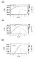
도 20(A) 및 도 20(B)는 시료 1의 트랜지스터의 BT시험 후의 Vg-Id 특성을 도시한 도면.
도 21(A) 및 도 21(B)는 시료 2의 트랜지스터의 BT시험 후의 Vg-Id 특성을 도시한 도면.
도 22는 XRD 스펙트럼을 설명하기 위한 도면.
도 23은 트랜지스터의 오프 전류를 설명하기 위한 도면.
도 24는 Id(실선) 및 전계 효과 이동도(점선)의 Vg 의존성을 설명하기 위한 도면.
도 25(A) 및 도 25(B)는 기판 온도와 임계 값 전압의 관계 및 기판 온도와 전계 효과 이동도의 관계를 설명하기 위한 도면.
도 26(A) 및 도 26(B)는 트랜지스터의 구조를 설명하기 위한 도면.
도 27(A) 및 도 27(B)는 트랜지스터의 구조를 설명하기 위한 도면.1 is a circuit diagram of a semiconductor device.
2 (A) and 2 (B) are circuit diagrams of a semiconductor device.
3 is a circuit diagram of a semiconductor device.
4 is a timing chart.
5A and 5B are sectional views and a plan view of a semiconductor device.
6A to 6D are cross-sectional views of the semiconductor device during a manufacturing step.
7A to 7D are cross-sectional views of the semiconductor device during a manufacturing step.
8A to 8D are cross sectional views of the semiconductor device during a manufacturing step;
9A to 9C are cross-sectional views of the semiconductor device during a manufacturing step.
10A to 10F are views for explaining electronic devices using semiconductor devices.
11A to 11E are views for explaining a crystal structure of an oxide material.
12A to 12C are views for explaining a crystal structure of an oxide material.
13A to 13C are views for explaining a crystal structure of an oxide material.
Fig. 14 is a diagram for explaining gate voltage dependency of mobility obtained by calculation.
15A to 15C are diagrams for explaining the gate voltage dependence of the calculated drain current and mobility.
16A to 16C are diagrams for explaining the gate voltage dependence of the drain current and mobility obtained by calculation.
17A to 17C are diagrams for explaining the gate voltage dependence of the drain current and mobility obtained by calculation.
18 (A) and 18 (B) are diagrams for explaining the cross-sectional structure of a transistor used for calculation.
19A to 19C are diagrams for explaining the characteristics of a transistor;
20A and 20B show the Vg -Id characteristics after the BT test of the transistor of
21 (A) and 21 (B) show Vg -Id characteristics after the BT test of the transistor of
22 is a diagram for explaining an XRD spectrum.
23 is a diagram for explaining an off current of a transistor;
FIG. 24 is a diagram for explaining Vg dependence of Id (solid line) and field effect mobility (dashed line). FIG.
25 (A) and 25 (B) are diagrams for explaining the relationship between the substrate temperature and the threshold voltage and the relationship between the substrate temperature and the field effect mobility.
26A and 26B are diagrams for explaining the structure of a transistor;
27A and 27B are diagrams for explaining the structure of a transistor;
개시하는 발명의 실시형태의 일례에 대하여 도면을 사용하여 이하에 설명한다. 다만, 본 발명은 이하의 설명에 한정되지 않고, 본 발명의 취지 및 그 범위에서 벗어남이 없이 그 형태 및 상세한 사항을 다양하게 변경할 수 있다는 것은 당업자라면 용이하게 이해할 수 있다. 따라서, 본 발명은 이하에 기재하는 실시형태의 기재 내용에 한정하여 해석되는 것은 아니다.An example of embodiment of the invention disclosed is demonstrated below using drawing. However, the present invention is not limited to the following description, and it can be easily understood by those skilled in the art that various changes can be made in form and detail without departing from the spirit and scope of the present invention. Therefore, this invention is not limited to description content of embodiment described below.
또한, 도면 등에서 도시하는 각 구성의 위치, 크기, 범위 등은 이해하기 쉽게 하기 위하여 실제의 위치, 크기, 범위 등을 도시하지 않는 경우가 있다. 따라서, 개시하는 발명은 반드시 도면 등에 개시된 위치, 크기, 범위 등에 한정되지 않는다.In addition, the position, size, range, etc. of each structure shown by drawing etc. may not show actual position, size, range, etc. for easy understanding. Accordingly, the disclosed invention is not necessarily limited to the position, size, range, and the like disclosed in the drawings and the like.
또한, 본 명세서 등에서 "위"나 "아래"라는 용어는 구성 요소의 위치 관계가 "바로 위" 또는 "바로 아래"인 것을 한정하는 것은 아니다. 예를 들어, "게이트 절연층 위의 게이트 전극"이라는 표현은 게이트 절연층과 게이트 전극 사이에 다른 구성 요소를 포함하는 것을 제외하지 않는다.In addition, the terms "up" and "down" in the present specification and the like do not limit that the positional relationship of the components is "directly up" or "directly down". For example, the expression “gate electrode on the gate insulating layer” does not exclude the inclusion of other components between the gate insulating layer and the gate electrode.
또한, "전극"이나 "배선"이라는 용어는 이들 구성 요소를 기능적으로 한정하는 것은 아니다. 예를 들어, "전극"은 "배선"의 일부분으로서 사용될 수 있고, "배선"은 "전극"의 일부분으로서 사용될 수 있다. 또한, "전극"이나 "배선"이라는 용어는 복수의 "전극"이나 "배선"이 일체가 되어 형성되는 경우 등도 포함한다.In addition, the terms "electrode" and "wiring" do not functionally limit these components. For example, "electrode" may be used as part of "wiring" and "wiring" may be used as part of "electrode". The term "electrode" or "wiring" also includes the case where a plurality of "electrodes" or "wiring" are formed integrally.
또한, "전기적으로 접속"한다는 표현에는 "어떤 전기적 작용을 갖는 것"을 통하여 접속되는 뜻도 포함된다. 여기서, "어떤 전기적 작용을 갖는 것"은 접속 대상 사이에서 전기 신호를 주고받고 할 수 있는 것이면 특별히 제한을 받지 않는다. 예를 들어, "어떤 전기적 작용을 갖는 것"에 전극이나 배선을 비롯하여 트랜지스터 등의 스위칭 소자, 저항 소자, 인덕터, 커패시터, 그 외 각종 기능을 갖는 소자 등이 포함된다.
In addition, the expression "electrically connected" includes the meaning of being connected through "having some electrical action". Here, the "having some electrical action" is not particularly limited as long as it can exchange electrical signals between objects to be connected. For example, the "having some electrical action" includes electrodes, wirings, switching elements such as transistors, resistance elements, inductors, capacitors, elements having various other functions, and the like.
(실시형태 1)(Embodiment 1)
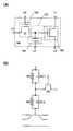
본 실시형태에서는 개시하는 발명의 일 형태에 따른 반도체 장치의 회로 구성 및 그 동작에 대하여 도면을 참조하여 설명한다. 또한, 회로도에서는 산화물 반도체를 사용한 트랜지스터임을 나타내기 위하여 "OS"의 부호를 함께 붙일 경우가 있다.In this embodiment, a circuit configuration and an operation of a semiconductor device of one embodiment of the disclosed invention will be described with reference to the drawings. Incidentally, in the circuit diagram, in order to indicate that the transistor uses an oxide semiconductor, the symbols "OS" may be attached together.
도 1은 본 발명의 일 형태인 반도체 장치의 회로 구성의 일례다. 제 1 트랜지스터(160), 제 2 트랜지스터(162), 용량 소자(164)를 포함하는 구성이 메모리 셀(190)이고, 도 1에 메모리 셀(190)이 1열당 m개 포함되는 구성이 n열 있는 예를 도시한다. 또한, m 및 n은 자연수다.1 is an example of a circuit configuration of a semiconductor device of one embodiment of the present invention. The configuration including the
여기서, 제 1 트랜지스터(160)는 특별히 한정되지 않는다. 정보의 판독 속도를 향상시키는 관점에서는, 예를 들어, 단결정 실리콘을 사용한 트랜지스터 등 스위칭 속도가 높은 트랜지스터를 적용하는 것이 바람직하다.Here, the
또한, 제 2 트랜지스터(162)에, 예를 들어, 산화물 반도체를 사용한 트랜지스터가 적용된다. 산화물 반도체를 사용한 트랜지스터는 오프 전류가 극히 작은 특징을 갖는다. 따라서, 제 2 트랜지스터(162)를 오프 상태로 함으로써 제 1 트랜지스터(160)의 게이트 전극의 전위를 극히 오랜 시간에 걸쳐 유지할 수 있다. 그리고, 용량 소자(164)를 가짐으로써 제 1 트랜지스터(160)의 게이트 전극에 공급된 전하의 유지가 용이해지고, 또한 유지된 정보의 판독이 용이해진다.In addition, for example, a transistor using an oxide semiconductor is applied to the
제 1 트랜지스터(160)는 제 2 트랜지스터(162)와 상이한 도전형을 갖도록 형성된다. 산화물 반도체를 사용하여 형성되는 제 2 트랜지스터가 n채널형인 경우에는 제 1 트랜지스터를 p채널형으로 한다.The
메모리 셀(190)에서 제 1 트랜지스터(160)의 게이트 전극과, 제 2 트랜지스터(162)의 소스 전극과, 용량 소자(164)의 전극의 한쪽이 전기적으로 접속된다.In the
비트선(BL_1 내지 BL_n)과 직교하는 워드선(WL_1 내지 WL_m+1)은 m+1개 형성되고, 제 1 선택선(SG1) 및 제 2 선택선(SG2) 각각이 제 1 선택 트랜지스터(180) 및 제 2 선택 트랜지스터(182)의 게이트 전극과 접속되도록 형성된다.M + 1 word lines WL_1 to WL_m + 1 orthogonal to the bit lines BL_1 to BL_n are formed, and each of the first select line SG1 and the second select line SG2 is the first
소스선(SL)은 제 2 선택 트랜지스터(182)를 통하여 제 m 메모리 셀의 제 1 트랜지스터의 소스 전극과 전기적으로 접속되고, 비트선은 제 1 선택 트랜지스터(180)를 통하여 제 1 메모리 셀의 제 1 트랜지스터의 드레인 전극과 전기적으로 접속된다.The source line SL is electrically connected to the source electrode of the first transistor of the mth memory cell through the second
제 1 워드선(WL_1)은 제 1 메모리 셀의 제 2 트랜지스터(162)의 게이트 전극과 전기적으로 접속된다. 또한, 제 k(k는 2 이상 m 이하의 자연수) 워드선은 제 k 메모리 셀의 제 2 트랜지스터의 게이트 전극과 전기적으로 접속됨과 함께, 제 k-1 메모리 셀의 용량 소자의 전극의 다른 쪽과 전기적으로 접속된다.The first word line WL_1 is electrically connected to the gate electrode of the
그리고, 제 k 메모리 셀의 제 1 트랜지스터의 드레인 전극이 제 k-1 메모리 셀의 제 1 트랜지스터의 소스 전극과 접속됨으로써 메모리 셀(190)은 소스선과 비트선 사이에서 전기적으로 접속되는 구성이 된다.The drain electrode of the first transistor of the kth memory cell is connected to the source electrode of the first transistor of the k-1 memory cell so that the
다음에, 메모리 셀(190)의 기본적인 회로 구성 및 그 동작에 대하여 도 2(A) 및 도 2(B)를 참조하여 설명한다. 또한, 여기서는, 제 1 트랜지스터(160)를 p채널형으로 하고, 제 2 트랜지스터(162)를 n채널형으로 한다.Next, the basic circuit configuration of the
도 2(A)에 도시한 반도체 장치에 있어서, 제 1 배선(L1)과 제 1 트랜지스터(160)의 드레인 전극(또는 소스 전극)은 전기적으로 접속되고, 또한, 제 2 배선(L2)과 제 1 트랜지스터(160)의 소스 전극(또는 드레인 전극)은 전기적으로 접속된다. 또한, 제 3 배선(L3)과 제 2 트랜지스터(162)의 드레인 전극(소스 전극)은 전기적으로 접속되고, 제 4 배선(L4)과 제 2 트랜지스터(162)의 게이트 전극은 전기적으로 접속된다. 그리고, 제 1 트랜지스터(160)의 게이트 전극 및 제 2 트랜지스터(162)의 소스 전극(또는 드레인 전극)은 용량 소자(164)의 한쪽의 전극과 전기적으로 접속되고, 제 5 배선(L5)과 용량 소자(164)의 다른 쪽의 전극은 전기적으로 접속된다.In the semiconductor device shown in FIG. 2A, the first wiring L1 and the drain electrode (or source electrode) of the
도 2(A)에 도시한 반도체 장치에서는 제 1 트랜지스터(160)의 게이트 전극의 전위를 유지할 수 있는 특징을 살림으로써, 이하에 기재하는 바와 같이, 정보의 기록, 유지, 판독이 가능하다.In the semiconductor device shown in FIG. 2A, by utilizing the feature that the potential of the gate electrode of the
우선, 정보의 기록 및 유지에 대하여 설명한다. 우선, 제 4 배선의 전위를 제 2 트랜지스터(162)가 온 상태가 되는 전위로 하여 제 2 트랜지스터(162)를 온 상태로 한다. 이로써, 제 3 배선의 전위가 제 1 트랜지스터(160)의 게이트 전극 및 용량 소자(164)에 공급된다. 즉, 제 1 트랜지스터(160)의 게이트 전극에 소정의 전하가 공급된다(기록). 여기서는, 2종류의 상이한 전위를 공급하기 위한 전하(이하, 저전위를 공급하기 위한 전하를 전하 QL, 고전위를 공급하기 위한 전하를 전하 QH라고 기재함) 중 어느 쪽이 공급되는 것으로 한다. 또한, 3종류 또는 그 이상의 상이한 전위를 공급하기 위한 전하를 적용하여 기억 용량을 향상시켜도 좋다. 그 후, 제 4 배선의 전위를 제 2 트랜지스터(162)가 오프 상태가 되는 전위로 하여 제 2 트랜지스터(162)를 오프 상태로 함으로써 제 1 트랜지스터(160)의 게이트 전극에 공급된 전하가 유지된다(유지).First, information recording and holding will be described. First, the
산화물 반도체를 사용하여 형성된 제 2 트랜지스터(162)의 오프 전류는 극히 작으므로 제 1 트랜지스터(160)의 게이트 전극의 전하는 오랜 시간에 걸쳐 유지된다.Since the off current of the
다음에, 정보의 판독에 대하여 설명한다. 제 1 배선에 소정의 전위(정(定)전위)를 공급한 상태에서 제 5 배선에 적절한 전위(판독 전위)를 공급하면, 제 1 트랜지스터(160)의 게이트 전극에 유지된 전하량에 따라 제 2 배선의 전위는 달라진다. 제 1 트랜지스터(160)가 p채널형인 경우에는, 제 1 트랜지스터(160)의 게이트 전극에 QH가 공급될 때 외견상의 임계 값 Vth_H는 제 1 트랜지스터(160)의 게이트 전극에 QL이 공급될 때의 외견상의 임계 값 Vth_L보다 낮기 때문이다. 여기서, 외견상의 임계 값이란 제 1 트랜지스터(160)를 "온 상태"로 하기 위하여 필요한 제 5 배선의 전위를 가리키는 것으로 한다. 따라서, 제 5 배선의 전위를 Vth_L와 Vth_H의 중간의 전위 V0로함으로써 제 1 트랜지스터(160)의 게이트 전극에 공급된 전하를 판별할 수 있다. 예를 들어, 기록 동작시에 QH가 공급된 경우에는, 제 5 배선의 전위가 V0(>Vth_H)이 되어도 제 1 트랜지스터(160)는 그대로 "오프 상태"다. QL이 공급된 경우에는, 제 5 배선의 전위가 V0(<Vth_L)이 되면 제 1 트랜지스터(160)는 "온 상태"가 된다. 따라서, 제 2 배선의 전위에 의하여 유지된 정보를 판독할 수 있다.Next, reading of the information will be described. If a suitable potential (reading potential) is supplied to the fifth wiring in a state where a predetermined potential (positive potential) is supplied to the first wiring, the second voltage is changed according to the amount of charge held in the gate electrode of the
또한, 도 1에 도시된 바와 같이, 메모리 셀을 어레이 형상으로 배치하여 사용하는 경우에는, 원하는 메모리 셀의 정보만을 판독할 수 있어야 한다. 이와 같이, 소정의 메모리 셀의 정보를 판독하고 그 외의 메모리 셀의 정보를 판독하지 않는 경우에는, 판독하는 대상이 아닌 메모리 셀의 제 5 배선에 게이트 전극의 상태에 상관없이 제 1 트랜지스터(160)가 "오프 상태"가 되는 전위, 즉, Vth_L보다 큰 전위를 공급하면 좋다. 또는, 게이트 전극의 상태에 상관없이 제 1 트랜지스터(160)가 "온 상태"가 되는 전위, 즉, Vth_H보다 작은 전위를 제 5 배선에 공급하면 좋다.In addition, as shown in FIG. 1, when the memory cells are arranged and used in an array shape, only the information of the desired memory cells should be read. As described above, when the information of the predetermined memory cell is read and the information of the other memory cells is not read, the
다음에, 정보의 재기록에 대하여 설명한다. 정보의 재기록은 상기 정보의 기록 및 유지와 마찬가지로 행해진다. 즉, 제 4 배선의 전위를 제 2 트랜지스터(162)가 온 상태가 되는 전위로 하여 제 2 트랜지스터(162)를 온 상태로 한다. 이로써, 제 3 배선의 전위(새로운 정보에 따른 전위)가 제 1 트랜지스터(160)의 게이트 전극 및 용량 소자(164)에 공급된다. 그 후, 제 4 배선의 전위를 제 2 트랜지스터(162)가 오프 상태가 되는 전위로 하여 제 2 트랜지스터(162)를 오프 상태로 함으로써 제 1 트랜지스터(160)의 게이트 전극은 새로운 정보에 따른 전하가 공급되고 유지된 상태가 된다.Next, rewriting of information will be described. Rewriting of information is performed in the same manner as recording and maintaining the information. That is, the
상술한 바와 같이, 개시하는 발명에 따른 반도체 장치는 정보를 다시 기록함으로써 직접적으로 정보를 재기록할 수 있다. 따라서, 플래시 메모리 등과 달리 고전압을 사용하여 부유 게이트로부터 전하를 뽑을 필요가 없고, 소거 동작에 기인한 동작 속도의 저하를 억제할 수 있다. 즉, 반도체 장치의 고속 동작이 실현된다.As described above, the semiconductor device according to the disclosed invention can directly rewrite information by rewriting the information. Therefore, unlike a flash memory or the like, it is not necessary to extract charges from the floating gate using a high voltage, and it is possible to suppress a decrease in the operation speed due to the erase operation. That is, high speed operation of the semiconductor device is realized.
또한, 제 2 트랜지스터(162)의 소스 전극(또는 드레인 전극)은 제 1 트랜지스터(160)의 게이트 전극과 전기적으로 접속됨으로써 비휘발성 메모리 소자로서 사용되는 부유 게이트형 트랜지스터의 부유 게이트와 동등한 작용을 갖는다. 이하에서, 제 2 트랜지스터(162)의 드레인 전극(또는 소스 전극)과 제 1 트랜지스터(160)의 게이트 전극이 전기적으로 접속되는 개소를 노드 FG라고 부를 경우가 있다. 제 2 트랜지스터(162)가 오프 상태인 경우에는, 상기 노드 FG는 절연체 내에 매설되어 있다고 볼 수 있고, 노드 FG에는 전하가 유지된다. 산화물 반도체를 사용한 제 2 트랜지스터(162)의 오프 전류는 실리콘 반도체로 형성되는 트랜지스터의 오프 전류의 10만분의 1 이하이므로, 제 2 트랜지스터(162)의 누설 전류로 인하여 노드 FG에 축적된 전하가 소실되는 것을 무시할 수 있다. 즉, 산화물 반도체를 사용한 제 2 트랜지스터(162)를 사용함으로써 전력이 공급되지 않아도 정보를 유지할 수 있는 비휘발성 기억 장치를 실현할 수 있다.In addition, the source electrode (or drain electrode) of the
예를 들어, 제 2 트랜지스터(162)의 실온(25℃)에서의 오프 전류가 10zA(1zA(zeptoampere))는 1×10-21A) 이하이고, 용량 소자(164)의 용량값이 10fF 정도인 경우에는 적어도 104초 이상의 데이터 유지가 가능하다. 또한, 상기 유지 시간이 트랜지스터 특성이나 용량값에 따라 변동하는 것은 두말할 나위가 없다.For example, the off current at room temperature (25 ° C.) of the
또한, 개시하는 발명에 따른 반도체 장치에서는 종래의 부유 게이트형 트랜지스터에서 지적되고 있는 게이트 절연층(터널 절연막)의 열화 문제가 없다. 즉, 전자를 부유 게이트에 주입할 때 게이트 절연층이 열화된다는 종래의 문제를 해소할 수 있다. 이것은 원리상 기록 횟수에 제한이 없다는 것을 의미한다. 또한, 종래의 부유 게이트형 트랜지스터에서 기록하거나 소거할 때 필요한 고전압도 불필요하다.In addition, in the semiconductor device according to the disclosed invention, there is no problem of deterioration of the gate insulating layer (tunnel insulating film) pointed out in the conventional floating gate type transistor. That is, the conventional problem that the gate insulating layer deteriorates when electrons are injected into the floating gate can be solved. This means that in principle, there is no limit to the number of recordings. In addition, the high voltage required for writing or erasing in the conventional floating gate transistor is also unnecessary.
도 2(A)에 도시한 반도체 장치는 상기 반도체 장치를 구성하는 트랜지스터 등의 요소가 저항 및 용량을 포함하는 것으로서 도 2(B)에 도시한 바와 같이 생각할 수 있다. 즉, 도 2(A)에서는 제 1 트랜지스터(160) 및 용량 소자(164)가 각각 저항 및 용량을 포함하고 구성된다고 생각한다. R1은 용량 소자(164)의 저항값이고, C1은 용량 소자(164)의 용량값이고, 저항값 R1은 용량 소자(164)를 구성하는 절연층의 저항값에 상당한다. 또한, R2는 제 1 트랜지스터(160)의 저항값이고, C2는 제 1 트랜지스터(160)의 용량값이고, 저항값 R2는 제 1 트랜지스터(160)가 온 상태일 때의 게이트 절연층의 저항값에 상당하고, 용량값 C2는 소위 게이트 용량(게이트 전극과 소스 전극 또는 드레인 전극 사이에 형성되는 용량, 및 게이트 전극과 채널 형성 영역 사이에 형성되는 용량)의 용량값에 상당한다.The semiconductor device shown in Fig. 2A can be considered as shown in Fig. 2B as elements such as transistors constituting the semiconductor device include resistance and capacitance. That is, in FIG. 2A, it is considered that the
제 2 트랜지스터(162)가 오프 상태인 경우의 소스 전극과 드레인 전극 사이의 저항값(실효 저항이라고도 부름)을 ROS로 하면, 제 2 트랜지스터(162)의 게이트 누설 전류가 충분히 작은 조건에서 R1 및 R2가 R1≥ROS(R1은 ROS 이상), R2≥ROS(R2는 ROS 이상)를 충족시키는 경우에는 전하의 유지 기간(정보의 유지 기간이라고도 할 수도 있음)은 주로 제 2 트랜지스터(162)의 오프 전류에 따라 결정된다.When the resistance value (also called the effective resistance) between the source electrode and the drain electrode when the
한편, 상기 조건을 충족시키지 않는 경우에는, 제 2 트랜지스터(162)의 오프 전류가 충분히 작아도 유지 기간을 충분히 확보하기 어렵다. 제 2 트랜지스터(162)의 오프 전류 외의 누설 전류(예를 들어, 제 1 트랜지스터(160)의 소스 전극과 게이트 전극 사이에 생기는 누설 전류 등)가 크기 때문이다. 이 이유로 본 실시형태에서 개시하는 반도체 장치는 R1≥ROS(R1은 ROS 이상) 및 R2≥ROS(R2는 ROS 이상)의 관계를 충족시키는 것이 바람직하다고 할 수 있다.On the other hand, when the above conditions are not satisfied, it is difficult to sufficiently maintain the sustain period even if the off current of the
한편, C1과 C2는 C1≥C2(C1은 C2 이상)의 관계를 충족시키는 것이 바람직하다. C1을 크게 함으로써 제 5 배선에 의하여 노드 FG의 전위를 제어할 때 제 5 배선의 전위를 효율 좋게 노드 FG에 공급할 수 있게 되고, 제 5 배선에 공급되는 전위(예를 들어, 판독 전위와 비판독 전위) 사이의 전위차를 낮게 억제할 수 있기 때문이다.On the other hand, it is preferable that C1 and C2 satisfy the relationship of C1? C2 (C1 is C2 or more). When C1 is increased, when the potential of the node FG is controlled by the fifth wiring, the potential of the fifth wiring can be efficiently supplied to the node FG, and the potential supplied to the fifth wiring (for example, read potential and non-reading). This is because the potential difference between the electric potentials) can be suppressed low.
상술한 관계를 충족시킴으로써 더 바람직한 반도체 장치를 실현할 수 있다. 또한, R1 및 R2는 제 1 트랜지스터(160)의 게이트 절연층이나 용량 소자(164)의 절연층에 의하여 제어할 수 있다. C1 및 C2에 대해서도 마찬가지다. 따라서, 게이트 절연층의 재료나 두께 등을 적절히 설정하여 상술한 관계를 충족시키도록 하는 것이 바람직하다.By satisfying the above-mentioned relationship, a more preferable semiconductor device can be realized. In addition, R1 and R2 can be controlled by the gate insulating layer of the
본 실시형태에 기재하는 반도체 장치에서는 노드 FG가 플래시 메모리 등의 부유 게이트형 트랜지스터의 부유 게이트와 마찬가지로 작용하지만, 본 실시형태의 노드 FG는 플래시 메모리 등의 부유 게이트와 본질적으로 상이한 특징을 갖는다.In the semiconductor device described in this embodiment, the node FG acts similarly to the floating gate of a floating gate type transistor such as a flash memory, but the node FG of the present embodiment has a feature that is essentially different from that of a floating gate such as a flash memory.
플래시 메모리에서는 컨트롤 게이트에 인가되는 전위가 높으므로 그 전위가 인접된 셀의 부유 게이트에 영향을 주지 않도록 셀과 셀의 간격을 어느 정도 유지할 필요가 생긴다. 이것은 반도체 장치의 고집적화를 저해하는 요인 중 하나다. 그리고, 상기 요인은 고전계를 인가하여 터널 전류를 발생시키는 플래시 메모리의 근본적인 원리에 기인하는 것이다.In a flash memory, since the potential applied to the control gate is high, it is necessary to maintain the cell-to-cell spacing to some extent so that the potential does not affect the floating gate of the adjacent cell. This is one of the factors that hinder the high integration of the semiconductor device. And, this factor is due to the fundamental principle of the flash memory to generate a tunnel current by applying a high field.
한편, 본 실시형태에 따른 반도체 장치는 산화물 반도체를 사용한 트랜지스터를 스위칭함으로써 동작하고, 상술한 바와 같은 터널 전류에 의한 전하 주입의 원리를 사용하지 않는다. 즉, 플래시 메모리와 같이 전하를 주입하기 위한 고전계가 불필요하다. 따라서, 컨트롤 게이트가 인접된 셀에 주는 고전계의 영향을 고려할 필요가 없으므로 고집적화가 용이해진다.On the other hand, the semiconductor device according to the present embodiment operates by switching a transistor using an oxide semiconductor, and does not use the principle of charge injection by tunnel current as described above. That is, a high electric field for injecting electric charge like a flash memory is unnecessary. Therefore, it is not necessary to take into account the influence of the high field that the control gate has on the adjacent cells, thereby facilitating high integration.
또한, 고전계가 불필요하고, 대형 주변 회로(승압 회로 등)가 불필요한 점도 플래시 메모리와 비교하여 유리한 점이다. 예를 들어, 본 실시형태에 따른 메모리 셀에 인가되는 전압(메모리 셀의 각 전극에 동시에 인가되는 최대 전위와 최소 전위의 차이)의 최대값은 2단계(1비트)의 정보를 기록하는 경우에 하나의 메모리 셀에서 5V 이하, 바람직하게는 3V 이하로 할 수 있다.In addition, a high electric field is unnecessary, and a large peripheral circuit (step-up circuit or the like) is unnecessary, which is advantageous in comparison with a flash memory. For example, when the maximum value of the voltage (difference between the maximum potential and the minimum potential applied simultaneously to each electrode of the memory cell) according to the present embodiment is recorded in two steps (one bit) of information, It can be 5V or less, preferably 3V or less in one memory cell.
또한, 용량 소자(164)를 구성하는 절연층의 비유전율 εr1과 제 1 트랜지스터(160)를 구성하는 절연층의 비유전율 εr2를 상이하게 하는 경우에는, 용량 소자(164)를 구성하는 절연층의 면적 S1과, 제 1 트랜지스터(160)에서 게이트 용량을 구성하는 절연층의 면적 S2가 2?S2≥S1(2?S2는 S1 이상) 바람직하게는 S2≥S1(S2는 S1 이상)을 충족시키면서 C1≥C2(C1은 C2 이상)를 실현하기 용이하다. 즉, 용량 소자(164)를 구성하는 절연층의 면적을 작게 하면서, C1≥C2를 실현하기 용이하다. 구체적으로는, 예를 들어, 용량 소자(164)를 구성하는 절연층에서는 산화하프늄 등의 high-k 재료로 이루어진 막, 또는 산화하프늄 등의 high-k 재료로 이루어진 막과 산화물 반도체로 이루어진 막의 적층 구조를 채용하여 εr1을 10 이상, 바람직하게는 15 이상으로 하고, 게이트 용량을 구성하는 절연층에서는 산화실리콘을 채용하여 εr2를 3 내지 4로 할 수 있다.In the case where the dielectric constant ε r1 of the insulating layer constituting the
이러한 구성을 함께 사용함으로써 개시하는 발명에 따른 반도체 장치를 한층 더 고집적화할 수 있다.By using such a configuration together, the semiconductor device according to the disclosed invention can be further integrated.
또한, 반도체 장치의 기억 용량을 크게 하기 위해서는 고집적화 외 다치화의 수법을 채용할 수도 있다. 예를 들어, 하나의 메모리 셀에 3단계 이상의 정보를 기록하는 구성으로 함으로써 2단계(1비트)의 정보를 기록하는 경우와 비교하여 기억 용량을 증대시킬 수 있다. 예를 들어, 상술한 바와 같이 저전위를 공급하기 위한 전하 QL, 고전위를 공급하기 위한 전하 QH에 추가하여, 다른 전위를 공급하기 위한 전하 Q를 제 1 트랜지스터의 게이트 전극에 공급함으로써 다치화를 실현할 수 있다.In addition, in order to increase the storage capacity of the semiconductor device, a method of high integration and multi-valued may be employed. For example, a configuration in which information of three or more levels is recorded in one memory cell can increase the storage capacity as compared with the case of writing information of two levels (one bit). For example, as described above, in addition to the charge QL for supplying the low potential and the charge QH for supplying the high potential, the charge Q for supplying another potential is supplied to the gate electrode of the first transistor. Achievement can be realized.
다음에, 메모리 셀 어레이 형상으로 배치한 반도체 장치의 동작에 대하여 설명한다.Next, the operation of the semiconductor device arranged in the shape of a memory cell array will be described.
우선, 메모리 셀을 구성하는 트랜지스터가 n채널형인 경우의 동작 방법의 일례에 대하여 설명한다. 도 3에 도시한 반도체 장치는 메모리 셀(191)을 어레이 위에 배치한 NAND형이고, 메모리 셀(191)이 1열당 m개 포함되는 구성이 n열 있는 예를 도시한다. 또한, m 및 n은 자연수다. 또한, 메모리 셀(191)은 메모리 셀(190)과 동등의 구성을 갖지만, 제 1 트랜지스터(161)가 n채널형인 것만이 상이하다.First, an example of the operation method in the case where the transistors constituting the memory cell are of n-channel type will be described. The semiconductor device shown in FIG. 3 is an NAND type in which
1번째 열의 제 1 메모리 셀(191)을 사용하여 설명하면, 도 2(A)에서의 제 1 배선(L1)은 제 1 비트선(BL_1), 제 2 배선(L2)은 소스선(SL), 제 3 배선(L3)은 제 2 비트선(BL_OS_1), 제 4 배선(L4)은 제 2 워드선(WL_OS_1), 제 5 배선(L5)은 제 1 워드선(WL_1)에 각각 상당한다.Referring to the
또한, 여기서는 일례로서 노드 FG에 전위 V2(전원 전위 VDD보다 낮은 전위) 또는 기준 전위 GND(0V) 중 한쪽을 공급하는 경우에 대해서 설명하지만, 노드 FG에 공급하는 전위의 관계는 이것에 한정되지 않는다. 또한, 노드 FG에 전위 V2를 공급한 경우에 유지되는 데이터를 데이터 "1", 노드 FG에 기준 전위 GND(0V)를 공급한 경우에 유지되는 데이터를 데이터 "0"으로 한다.Here, as an example, the case where one of the potential V2 (the potential lower than the power supply potential VDD) or the reference potential GND (0 V) is supplied to the node FG will be described. However, the relationship between the potential supplied to the node FG is not limited to this. . The data held when the potential V2 is supplied to the node FG is data "1", and the data held when the reference potential GND (0V) is supplied to the node FG is data "0".
우선, 제 1 선택선(SG1)의 전위를 GND(0V)로 하고, 제 2 선택선(SG2)의 전위를 V1(예를 들어, VDD)로 하고, 기록 대상의 메모리 셀(191)에 접속되는 제 2 워드선(WL_OS)의 전위를 V3(V2보다 높은 전위, 예를 들어, VDD)으로 하여 메모리 셀(191)을 선택한다.First, the potential of the first selection line SG1 is set to GND (0 V), the potential of the second selection line SG2 is set to V1 (for example, VDD), and connected to the
메모리 셀(191)에 데이터 "0"을 기록하는 경우에는, 제 2 비트선(BL_OS)에 GND를 공급하고, 메모리 셀(191)에 데이터 "1"을 기록하는 경우에는, 제 2 비트선(BL_OS)에 V2를 공급한다. 여기서는, 제 2 워드선(WL_OS)의 전위를 V3으로 하기 때문에 노드 FG에 V2를 공급할 수 있다.When data "0" is written to the
유지 대상인 메모리 셀(191)에 접속되는 제 2 워드선(WL_OS)의 전위를 GND로 함으로써 데이터가 유지된다. 제 2 워드선(WL_OS)의 전위를 GND로 고정하면, 노드 FG의 전위는 기록시의 전위로 고정된다. 즉, 노드 FG에 데이터 "1"인 V2가 공급되는 경우에는, 노드 FG의 전위는 V2가 되고, 노드 FG에 데이터 "0"인 GND(0V)가 공급되면, 노드 FG의 전위는 GND(0V)가 된다.Data is retained by setting the potential of the second word line WL_OS connected to the
또한, 제 2 워드선(WL_OS)에는 GND(0V)가 공급되기 때문에, 데이터 "1"과 데이터 "0" 중 어느 쪽이 기록된 경우라도, 제 2 트랜지스터(162)는 오프 상태가 된다. 제 2 트랜지스터(162)의 오프 전류는 매우 작기 때문에, 제 1 트랜지스터(161)의 게이트 전극의 전하는 오랜 시간에 걸쳐 유지된다.In addition, since GND (0V) is supplied to the second word line WL_OS, even when either data "1" or data "0" is written, the
판독 대상인 메모리 셀(191)에 접속되는 제 1 워드선(WL)의 전위를 GND(0V)로 하고, 또한, 판독 대상이 아닌 메모리 셀(191)에 접속되는 제 1 워드선(WL)의 전위를 V5(예를 들어, VDD)로 하고 또 제 1 선택선(SG1) 및 제 2 선택선(SG2)의 전위를 V1로 하고, 제 1 선택 트랜지스터(181) 및 제 2 선택 트랜지스터(183)를 온 상태로 함으로써 데이터가 판독된다. 또한, 제 1 비트선(BL)에 필요한 전위 V6(예를 들어, VDD 이하의 전위)를 공급하면 좋다.The potential of the first word line WL connected to the
판독 대상인 메모리 셀(191)에 접속되는 제 1 워드선(WL)의 전위를 GND(0V)로 하면, 판독 대상인 메모리 셀(191)의 노드 FG에 데이터 "1"인 V2가 공급되는 경우에는 제 1 트랜지스터(161)는 온 상태가 된다. 한편, 노드 FG에 데이터 "0"인 GND(0V)가 공급되는 경우에는 제 1 트랜지스터(161)는 오프 상태가 된다.When the potential of the first word line WL connected to the
또한, 판독 대상이 아닌 메모리 셀(191)에 접속되는 제 1 워드선(WL)의 전위를 V5로 하면, 판독 대상이 아닌 메모리 셀(191)에 데이터 "1"이 기록된 경우 또는 데이터 "0"이 기록된 경우의 어느 경우라도 제 1 트랜지스터(161)는 온 상태가 된다. 상술한 바와 같이, 유지된 정보를 판독할 수 있다.Further, when the potential of the first word line WL connected to the
여기서, 상기 동작에 따른 도 3의 반도체 장치에서의 배선 개수는 워드선(WL, WL_OS)이 2m개, 비트선(BL, BL_OS)이 2n개, 소스선(SL)이 1개, 선택선(SG)이 2개이고, 워드선과 비트선만으로도 하나의 메모리 셀당 4개의 배선이 필요하다. 따라서, 회로 면적을 축소할 수 없고, 단위 면적당의 기억 용량을 증가시키기 어려웠다.The number of wirings in the semiconductor device of FIG. 3 according to the above operation is 2 m in word lines WL and WL_OS, 2n in bit lines BL and BL_OS, 1 in source line SL, and selection line ( SG) is two, and only four word lines and four bit lines are required for one memory cell. Therefore, the circuit area cannot be reduced and it is difficult to increase the storage capacity per unit area.
다음에, 본 발명의 일 형태인 도 1의 반도체 장치의 동작에 대하여 도 4의 타이밍 차트를 사용하여 설명한다. 또한, 도 1의 반도체 장치에서의 배선 개수는 워드선(WL)이 m+1개, 비트선(BL)이 n개, 소스선(SL)이 1개, 선택선(SG)이 2개다. 즉, 기록용 워드선과 판독용 워드선을 공통적으로 사용하고, 또 기록용 비트선과 판독용 비트선을 공통적으로 사용함으로써 배선 개수를 삭감한 것이다.Next, the operation of the semiconductor device of FIG. 1, which is one embodiment of the present invention, will be described using the timing chart of FIG. 4. The number of wirings in the semiconductor device of FIG. 1 is m + 1 word lines WL, n bit lines BL, one source line SL, and two selection lines SG. That is, the number of wirings is reduced by using the write word line and the read word line in common, and the write bit line and the read bit line in common.
또한, 여기서는 일례로서 노드 FG에 전위 V1(예를 들어, VDD) 또는 기준 전위 GND(0V) 중 어느 쪽을 공급하는 경우에 대하여 설명하지만, 노드 FG에 공급하는 전위의 관계는 이것에 한정되지 않는다. 또한, 노드 FG에 전위 V1을 공급한 경우에 유지되는 데이터를 데이터 "1", 노드 FG에 기준 전위 GND(0V)를 공급한 경우에 유지되는 데이터를 데이터 "0"으로 한다.In addition, although the case where either the potential V1 (for example, VDD) or the reference potential GND (0V) is supplied to the node FG as an example is demonstrated, the relationship of the potential supplied to the node FG is not limited to this. . The data held when the potential V1 is supplied to the node FG is data "1", and the data held when the reference potential GND (0 V) is supplied to the node FG is data "0".
본 실시형태에서는 설명의 간이화를 위하여 1번째 행 1번째 열의 메모리 셀에 데이터 "1"을 기록하고 1번째 행 n번째 열의 메모리 셀에 데이터 "0"을 기록하는 경우를 설명한다. 우선, 기록시에는 직렬된 제 1 트랜지스터(160)가 도통하지 않도록 제 1 선택선(SG1) 및 제 2 선택선(SG2)의 전위를 V1로 하고, 제 1 선택 트랜지스터(180) 및 제 2 선택 트랜지스터(182)를 확실히 오프 상태로 한다.In the present embodiment, for the sake of simplicity, a case where data "1" is written in the memory cells of the first row and the first column and data "0" is written into the memory cells of the first row and the nth column will be described. First, at the time of writing, the potentials of the first select line SG1 and the second select line SG2 are set to V1 so that the
기록 행의 워드선(WL_1)의 전위를 V1로 하고, 그 외의 워드선의 전위를 GND로 한다. 이 때, 제 2 트랜지스터(162)의 임계 값 전압(Vth_OS)이 V1>Vth_OS>0V(GND)의 관계를 충족시킨다면, 1번째 행의 제 2 트랜지스터(162)는 온 상태가 되고, 그 외의 행의 제 2 트랜지스터(162)는 오프 상태가 된다.The potential of the word line WL_1 in the write row is set to V1, and the potential of the other word lines is set to GND. At this time, if the threshold voltage Vth _OS of the
여기서, 1번째 열의 비트선(BL_1)의 전위를 V1로 하고 n번째 열의 비트선(BL_n)의 전위를 GND로 함으로써, 1번째 행 1번째 열의 노드 FG의 전위가 V1이 되고, 1번째 행 n번째 열의 노드 FG의 전위가 0V가 된다.Here, by setting the potential of the bit line BL_1 of the first column to V1 and the potential of the bit line BL_n of the nth column to GND, the potential of the node FG in the first row and the first column becomes V1, and the first row n The potential of the node FG in the first column becomes 0V.
그리고, 워드선(WL_1)의 전위를 GND(0V)로 하고, 1번째 행의 제 2 트랜지스터(162)를 오프 상태로 하면, 노드 FG의 전위는 각각 유지된다.When the potential of the word line WL_1 is set to GND (0V) and the
또한, 워드선(WL_1)에는 GND(0V)가 공급되기 때문에 데이터 "1"과 데이터 "0" 중 어느 쪽이 기록된 경우라도 제 2 트랜지스터(162)는 오프 상태가 된다. 제 2 트랜지스터(162)의 오프 전류는 극히 작으므로 제 1 트랜지스터(160)의 게이트 전극의 전하는 오랜 시간에 걸쳐 유지된다.In addition, since the GND (0V) is supplied to the word line WL_1, the
다음에, 도 4의 타이밍 차트를 사용하여 1번째 행의 메모리 셀에서 데이터를 판독하는 경우를 설명한다.Next, the case of reading data from the memory cells of the first row using the timing chart of FIG. 4 will be described.
우선, 판독시에는 직렬된 제 1 트랜지스터(160)가 도통하도록 제 1 선택선(SG1) 및 제 2 선택선(SG2)의 전위를 V2로 하여 제 1 선택 트랜지스터(180) 및 제 2 선택 트랜지스터(182)를 온 상태로 한다. 그리고, 판독 행(1번째 행)의 하나 아래의 행에서의 워드선(WL2)의 전위를 V2로 하고, 워드선(WL_1)의 전위를 0V(또는, Vth_OS 이하의 전위)로 하고, 그 외의 워드선의 전위를 V3으로 한다. 결과적으로, 판독 행 외의 모든 제 1 트랜지스터(160)는 메모리 셀의 데이터 상태에 의하지 않고 온 상태가 된다.First, in reading, the first
여기서, 워드선(WL_1) 외의 워드선에 p채널형 제 1 트랜지스터(160)를 동작시키기 위한 음 전위가 인가된다. 따라서, 각각의 워드선에 접속된 n채널형 제 2 트랜지스터(162)는 온 상태가 되지 않고, 노드 FG의 전위는 유지된다.Here, a negative potential for operating the p-channel
한편, 판독 행에서의 제 1 트랜지스터(160)의 동작 상태는 메모리 셀에 유지된 데이터에 의존한다. 즉, 제 1 트랜지스터(160)는 데이터 "0"이 유지된 1번째 행 n번째 열에서는 온 상태가 되고, 데이터 "1"이 유지된 1번째 행 1번째 열에서는 오프 상태가 된다.On the other hand, the operating state of the
결과적으로, 모든 비트선의 전위를 V1로 하였을 때, 전위가 0V인 소스선(SL)과 비트선(BL_n)은 통전하고, 비트선(BL_n)의 전위는 0V로 수속한다. 또한, 비트선(BL_1)에서는 전위 V1이 유지된다. 상술한 바와 같이, 유지된 정보를 판독할 수 있다.As a result, when the potential of all the bit lines is set to V1, the source line SL and the bit line BL_n having the potential of 0 V are energized, and the potential of the bit line BL_n converges to 0 V. As shown in FIG. In the bit line BL_1, the potential V1 is held. As described above, the retained information can be read.
여기서, 제 1 트랜지스터(160)는 노멀리 오프(게이트 전압이 0V일 때 오프 상태가 됨)가 되는 p채널형이고, 유지 용량의 전위를 더한 임계 값 전압이 데이터 "0"일 때 Vth0이고 데이터 "1"일 때 Vth1이면, V3<Vth1<V2<Vth0<0V의 관계가 있는 것으로 한다.Here, the
또한, 도 1에서 제 1 선택선(SG1) 및 제 1 선택 트랜지스터(180), 또는 제 2 선택선(SG2) 및 제 2 선택 트랜지스터(182) 중 한 쌍을 생략한 구성으로 할 수도 있다. 이 경우에도, 데이터의 기록, 유지, 및 판독은 기본적으로 상술한 동작과 마찬가지로 행할 수 있다.In addition, in FIG. 1, a pair of the first select line SG1 and the first
상술한 바와 같이, 도 3의 구성보다 신호선(배선 개수)을 삭감한 구성에서도 노드 FG에 데이터를 유지하고 노드 FG로부터 데이터를 판독할 수 있는 반도체 장치의 동작이 설명되었다. 따라서, 본 발명의 일 형태에 따른 반도체 장치의 구성을 사용하면, 회로 면적을 삭감할 수 있고, 단위 면적당의 기억 용량을 증가시킬 수 있다.As described above, the operation of the semiconductor device capable of retaining data at the node FG and reading data from the node FG even in the configuration in which the signal lines (the number of wirings) are reduced from the configuration in FIG. 3 has been described. Therefore, by using the configuration of the semiconductor device of one embodiment of the present invention, the circuit area can be reduced, and the storage capacity per unit area can be increased.
또한, 제 2 트랜지스터(162)를 메모리 셀 사이에서 직렬로 접속함으로써 비트선을 삭감할 수 있지만, 이 경우에는, 데이터를 재기록할 때 모든 비트를 소거해야 한다. 한편, 본 발명의 일 형태에 따른 반도체 장치의 구성에서는 제 2 트랜지스터(162)는 메모리 셀 사이에서 직렬로 접속되지 않고 모든 비트를 소거할 필요가 없으므로 랜덤 액세스성이 뛰어나고 소비 전력을 억제할 수도 있다.In addition, although the bit lines can be reduced by connecting the
본 실시형태에 기재하는 구성, 방법 등은 다른 실시형태에 기재하는 구성, 방법 등과 적절히 조합하여 사용할 수 있다.
The structure, method, etc. which are described in this embodiment can be used in appropriate combination with the structure, method, etc. which are described in another embodiment.
(실시형태 2)(Embodiment 2)
본 실시형태에서는 개시하는 발명의 일 형태에 따른 반도체 장치의 구성 및 그 제작 방법에 대하여 도면을 참조하여 설명한다.In this embodiment, the structure and manufacturing method of the semiconductor device of one embodiment of the disclosed invention will be described with reference to the drawings.
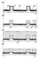
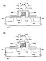
도 5(A) 및 도 5(B)는 도 1의 회로도를 사용하여 설명한 반도체 장치(메모리 셀(190) 및 제 1 선택 트랜지스터(180))의 구성의 일례이다. 도 5(A)에 반도체 장치의 단면을 도시하고, 도 5(B)에 반도체 장치의 평면을 도시한다. 여기서, 도 5(A)는 도 5(B)의 선 A1-A2로 절단한 단면에 상당한다. 또한, 도 5(B)에서 선 A1-A2에 평행한 방향이 도 1의 회로도에서 열 방향에 상당하고, 선 A1-A2에 수직인 방향이 도 1의 회로도에서 행 방향에 상당한다. 또한, 도 5(B)는 설명의 간이화를 위하여 배선(전극) 등을 강조하여 도시하고 절연층 등을 생략한 것이다.5A and 5B are examples of the configuration of the semiconductor device (
도 5(A) 및 도 5(B)에 도시된 반도체 장치는 하부에 제 1 반도체 재료를 사용한 제 1 트랜지스터(160) 및 제 1 선택 트랜지스터(180)를 갖고, 상부에 제 2 반도체 재료를 사용한 제 2 트랜지스터(162)를 갖는 것이다. 또한, 도 5(A) 및 도 5(B)에서는 제 1 번째 행의 제 1 트랜지스터(160) 및 제 2 트랜지스터(162)를 도시하지만, 도 1의 회로도에 도시한 바와 같이, 제 1 번째 행 내지 제 m 번째 행까지 제 1 트랜지스터(160)는 소스 전극(소스 영역)과 드레인 전극(드레인 영역)이 직렬로 접속된다.The semiconductor device shown in Figs. 5A and 5B has a
여기서, 제 1 반도체 재료와 제 2 반도체 재료는 상이한 재료인 것이 바람직하다. 예를 들어, 제 1 반도체 재료를 산화물 반도체 외의 반도체 재료(실리콘 등)로 하고, 제 2 반도체 재료를 산화물 반도체로 할 수 있다. 단결정 실리콘 등의 산화물 반도체 외의 재료를 사용한 트랜지스터는 고속 동작이 용이하다. 한편, 산화물 반도체를 사용한 트랜지스터는 그 특성에 의하여 오랜 시간에 걸쳐 전하를 유지할 수 있다.Here, it is preferable that a 1st semiconductor material and a 2nd semiconductor material are different materials. For example, the first semiconductor material may be a semiconductor material other than an oxide semiconductor (silicon or the like), and the second semiconductor material may be an oxide semiconductor. Transistors using materials other than oxide semiconductors such as single crystal silicon can be easily operated at high speed. On the other hand, a transistor using an oxide semiconductor can retain charge over a long time due to its characteristics.
또한, 도 1의 회로 구성에 의거하여 제 1 트랜지스터(160)는 p채널형, 제 2 트랜지스터(162)는 n채널형인 것으로 가정하여 설명하지만, 제 1 트랜지스터(160)를 n채널형, 제 2 트랜지스터(162)를 p채널형으로 하여도 동작시킬 수 있다. 또한, 개시하는 발명의 기술적인 본질은 정보를 유지하기 위하여 산화물 반도체와 같은 오프 전류를 충분히 저감할 수 있는 반도체 재료를 제 2 트랜지스터(162)에 사용하는 점에 있기 때문에, 반도체 장치에 사용되는 재료나 반도체 장치의 구조 등 반도체 장치의 구체적인 구성은 여기에 기재하는 것에 한정할 필요는 없다.1, the
도 5(A) 및 도 5(B)에 도시한 제 1 트랜지스터(160)는 반도체 재료(예를 들어, 실리콘 등)를 포함하는 기판(100)에 제공된 채널 형성 영역(116a), 채널 형성 영역(116a)을 끼우도록 제공된 불순물 영역(120a) 및 불순물 영역(120b), 불순물 영역(120a) 및 불순물 영역(120b)과 접촉되는 금속 화합물 영역(124a) 및 금속 화합물 영역(124b), 채널 형성 영역(116a) 위에 제공된 게이트 절연층(108a), 게이트 절연층(108a) 위에 제공된 게이트 전극(110a)을 포함하여 구성된다.The
또한, 도면에 소스 전극이나 드레인 전극을 명시적으로 도시하지 않는 경우가 있지만, 편의상 이러한 상태를 포함하여 트랜지스터라고 부를 경우가 있다. 또한, 이 경우에는 트랜지스터의 접속 관계를 설명하기 위하여 소스 영역이나 드레인 영역을 포함하여 소스 전극이나 드레인 전극이라고 표현할 경우가 있다. 즉, 본 명세서에서 소스 전극이라고 기재하면 소스 영역이 포함될 수 있고, 드레인 전극이라고 기재하면 드레인 영역이 포함될 수 있다.In addition, although the source electrode and the drain electrode are not explicitly shown in the figure, for convenience, it may be called a transistor including such a state. In this case, in order to explain the connection relationship between transistors, it may be expressed as a source electrode or a drain electrode including a source region and a drain region. That is, in the present specification, when described as a source electrode, a source region may be included, and when described as a drain electrode, a drain region may be included.
또한, 본 명세서 중에서 불순물 영역(120a), 불순물 영역(120b), 및 후술하는 불순물 영역(120c)을 총칭하여 불순물 영역(120)이라고 기재하는 경우가 있다. 또한, 본 명세서 중에서 금속 화합물 영역(124a), 금속 화합물 영역(124b), 및 후술하는 금속 화합물 영역(124c)을 총칭하여 금속 화합물 영역(124)이라고 기재하는 경우가 있다.In addition, in this specification, the
여기서, 제 1 트랜지스터(160)는 소스 영역 또는 드레인 영역으로서 기능하는 불순물 영역(120) 및 금속 화합물 영역(124)을 공유하고, 제 1 번째 행 내지 제 m번째 행까지 직렬로 접속된다. 즉, 제 k-1 번째 행(k는 2 이상 m 이하의 자연수)의 제 1 트랜지스터(160)의 소스 영역으로서 기능하는 불순물 영역(120) 및 금속 화합물 영역(124)은 제 k 번째 행의 제 1 트랜지스터(160)의 드레인 영역으로서 기능한다.Here, the
이와 같이, 메모리 셀(190)의 제 1 트랜지스터(160)를 직렬로 접속함으로써 각 메모리 셀(190) 사이에서 제 1 트랜지스터(160)의 소스 영역 및 드레인 영역을 공유할 수 있다. 즉, 각 메모리 셀(190)에서 제 1 트랜지스터(160)의 소스 영역 또는 드레인 영역의 한쪽을 개구부를 형성함으로써 배선(158)에 별도로 접속할 필요가 없다. 따라서, 제 1 트랜지스터(160)의 평면 레이아웃은 배선(158)과 접속하기 위한 개구를 형성할 필요가 없으므로, 후술하는 제 2 트랜지스터(162)의 평면 레이아웃에 용이하게 중첩할 수 있어 메모리 셀(190)의 점유 면적의 저감을 도모할 수 있다.As such, by connecting the
또한, 제 1 번째 행의 제 1 트랜지스터(160)는 제 1 선택 트랜지스터(180)를 통하여 비트선(BL)과 전기적으로 접속되므로, 제 1 번째 행의 제 1 트랜지스터(160)의 드레인 영역으로서 기능하는 불순물 영역(120b) 및 금속 화합물 영역(124b)은 제 1 선택 트랜지스터(180)의 소스 영역으로서 기능한다. 여기서, 제 1 선택 트랜지스터(180)는 상술한 제 1 트랜지스터(160)와 같은 구성으로 할 수 있다.In addition, since the
즉, 제 1 선택 트랜지스터(180)는 반도체 재료(예를 들어, 실리콘 등)를 함유한 기판(100)에 제공된 채널 형성 영역(116b)과, 채널 형성 영역(116b)을 끼우도록 제공된 불순물 영역(120b) 및 불순물 영역(120c)과, 불순물 영역(120b) 및 불순물 영역(120c)과 접촉되는 금속 화합물 영역(124b) 및 금속 화합물 영역(124c)과, 채널 형성 영역(116b) 위에 제공된 게이트 절연층(108b)과, 게이트 절연층(108b) 위에 제공된 게이트 전극(110b)을 갖는다. 또한, 제 1 선택 트랜지스터(180)의 게이트 전극(110b)은 도 1에 도시한 회로도에서의 선택선 SG로서 기능한다.That is, the
또한, 본 명세서에서 채널 형성 영역(116a) 및 채널 형성 영역(116b)을 총칭하여 채널 형성 영역(116)이라고 기재하는 경우가 있다. 또한, 본 명세서에서 게이트 절연층(108a) 및 게이트 절연층(108b)을 총칭하여 게이트 절연층(108)이라고 기재하는 경우가 있다. 또한, 본 명세서에서 게이트 전극(110a) 및 게이트 전극(110b)을 총칭하여 게이트 전극(110)이라고 기재하는 경우가 있다.In addition, in this specification, the
또한, 기판(100) 위에 제 1 트랜지스터(160) 및 제 1 선택 트랜지스터(180)를 둘러싸도록 소자 분리 절연층(106)이 제공되고, 제 1 트랜지스터(160) 및 제 1 선택 트랜지스터(180) 위에 게이트 전극(110)의 상면을 노출시키도록 절연층(128)이 제공된다. 또한, 고집적화를 실현하기 위해서는 도 5(A) 및 도 5(B)에 도시한 바와 같이, 제 1 트랜지스터(160)가 사이드 월 절연층을 갖지 않는 구성으로 하는 것이 바람직하다. 한편, 제 1 트랜지스터(160)의 특성을 중요시하는 경우에는, 게이트 전극(110) 측면에 사이드 월 절연층을 제공하고, 불순물 농도가 상이한 영역을 포함하는 불순물 영역(120)을 제공하여도 좋다.In addition, a device
여기서, 절연층(128)은 평탄성이 양호한 표면을 갖는 것이 바람직하고, 예를 들어, 절연층(128)의 표면은 제곱 평균 평방근 거칠기(RMS)를 1nm 이하로 하는 것이 바람직하다.Here, the insulating
도 5(A) 및 도 5(B)에서의 제 2 트랜지스터(162)는 절연층(128) 위에 형성된 소스 전극(142a) 및 드레인 전극(142b)과, 절연층(128), 소스 전극(142a) 및 드레인 전극(142b)의 일부분과 접촉되는 산화물 반도체층(144)과, 산화물 반도체층(144)을 덮는 게이트 절연층(146)과, 게이트 절연층(146) 위에 산화물 반도체층(144)과 중첩되도록 제공된 게이트 전극(148)을 갖는다. 또한, 게이트 전극(148)은 도 1에 도시한 회로도에서의 워드선 WL로서 기능한다.The
또한, 도 5(A) 및 도 5(B)에서 제 2 트랜지스터(162)는 톱 게이트 보텀 콘택트형(TGBC형)의 구성을 도시한 것이지만, 도시된 구성에 한정되지 않는다. 예를 들어, 톱 게이트 톱 콘텍트형(TGTC형), 보텀 게이트 보텀 콘택트형(BGBC형), 보텀 게이트 톱 콘텍트형(BGTC형) 등의 구성이라도 좋다.In addition, although the
또한, 도시하지 않았지만, 소스 전극(142a)과 산화물 반도체층(144) 사이 및 드레인 전극(142b)과 산화물 반도체층(144) 사이에 n형 도전형을 갖는 버퍼층을 제공하여도 좋다. 상기 버퍼층을 형성함으로써 소스 전극(142a)과 산화물 반도체층(144) 사이 및 드레인 전극(142b)과 산화물 반도체층(144) 사이의 접촉 저항을 낮출 수 있고 트랜지스터의 온 전류를 증가시킬 수 있다.Although not shown, a buffer layer having an n-type conductivity may be provided between the
n형 도전형을 갖는 버퍼층에 사용할 수 있는 대표적인 재료로서는, 인듐 산화물(In-O계), 인듐주석 산화물(In-Sn-O계), 인듐아연 산화물(In-Zn-O계), 주석 산화물(Sn-O계), 아연 산화물(Zn-O계), 주석아연 산화물(Sn-Zn-O계) 등의 금속 산화물이 있고, 그것에 알루미늄(Al), 갈륨(Ga), 실리콘(Si) 중에서 선택된 원소가 하나 이상 함유되어도 좋다. 또한, 티타늄 산화물(Ti-O), 티타늄니오븀 산화물(Ti-Nb-O계), 몰리브덴 산화물(Mo-O계), 텅스텐 산화물(W-O계), 마그네슘 산화물(Mg-O계), 칼슘 산화물(Ca-O계), 갈륨 산화물(Ga-O계) 등을 사용할 수 있다. 또한, 상기 재료에 질소(N)가 함유되어도 좋다.Representative materials that can be used for the buffer layer having an n-type conductivity type include indium oxide (In-O-based), indium tin oxide (In-Sn-O-based), indium zinc oxide (In-Zn-O-based), and tin oxide. Metal oxides such as (Sn-O-based), zinc oxide (Zn-O-based), tin zinc oxide (Sn-Zn-O-based), and the like, among which aluminum (Al), gallium (Ga), and silicon (Si) One or more selected elements may be contained. Further, titanium oxide (Ti-O), titanium niobium oxide (Ti-Nb-O-based), molybdenum oxide (Mo-O-based), tungsten oxide (WO-based), magnesium oxide (Mg-O-based), calcium oxide ( Ca-O-based), gallium oxide (Ga-O-based) and the like can be used. In addition, nitrogen (N) may be contained in the material.
여기서, 산화물 반도체층(144)은 수소 등의 불순물이 충분히 제거됨으로써 또는 충분히 산소가 공급됨으로써 고순도화된 것이 바람직하다. 구체적으로는, 예를 들어, 산화물 반도체층(144)의 수소 농도는 5×10¹⁹atoms/cm3 이하, 바람직하게는 5×10¹⁸atoms/cm3 이하, 더 바람직하게는 5×10¹⁷atoms/cm3 이하로 한다. 또한, 상술한 산화물 반도체층(144) 중의 수소 농도는 2차 이온 질량 분석법(SIMS: Secondary Ion Mass Spectrometry)으로 측정되는 것이다. 이와 같이, 수소 농도가 충분히 저감되어 고순도화되고, 충분히 산소가 공급됨으로써 산소 결손에 기인한 에너지 갭 중의 결함 준위가 저감된 산화물 반도체층(144)에서는 수소 등의 도너에 기인한 캐리어 밀도가 1×10¹²/cm3 미만, 바람직하게는 1×10¹¹/cm3 미만, 더 바람직하게는 1.45×10¹⁰/cm3 미만이다. 또한, 예를 들어, 실온(25℃)에서의 오프 전류(여기서는, 단위 채널 폭(1μm)당의 값)는 100zA(1zA(zeptoampere)는 1×10-21A) 이하, 바람직하게는 10zA 이하다. 이와 같이, i형화(진성화) 또는 실질적으로 i형화된 산화물 반도체를 사용함으로써 극히 뛰어난 오프 전류 특성을 갖는 트랜지스터를 얻을 수 있다.Here, the
또한, 절연층(128) 표면이고 산화물 반도체층(144)과 접촉되는 영역은 그 제곱 평균 평방근 거칠기(RMS)를 1nm 이하로 하는 것이 바람직하다. 이와 같이, 제곱 평균 평방근 거칠기(RMS)가 1nm 이하로 극히 평탄한 영역에 제 2 트랜지스터(162)의 채널 형성 영역을 제공함으로써 제 2 트랜지스터(162)가 미세화되는 상황에서도 단채널 효과 등의 문제가 일어나는 것을 방지하고, 양호한 특성을 갖는 제 2 트랜지스터(162)를 제공할 수 있다.In addition, the area of the insulating
도 5(A) 및 도 5(B)에서의 용량 소자(164)는 소스 전극(142a), 산화물 반도체층(144), 게이트 절연층(146), 게이트 절연층(146) 위의 절연층(150), 및 전극(152)을 포함하여 구성된다. 즉, 소스 전극(142a)은 용량 소자(164)의 한쪽의 전극으로서 기능하고, 전극(152)은 용량 소자(164)의 다른 쪽의 전극으로서 기능한다. 또한, 용량 소자(164)는 게이트 절연층(146)을 포함하지 않는 구성으로 하여도 좋다. 이러한 구성으로 함으로써 용량 소자(164)의 유전체층은 산화물 반도체층(144)과 절연층(150)으로 구성되므로 유전체층의 막 두께가 저감되고 용량 소자(164)의 정전 용량을 증가시킬 수 있다.The
여기서, 제 k-1번째 행(k는 2 이상 m 이하의 자연수)의 용량 소자(164)의 한쪽의 전극은 제 k-1번째 행의 제 2 트랜지스터(162)의 소스 전극(142a)이므로, 용량 소자(164)의 평면 레이아웃은 제 2 트랜지스터(162)의 평면 레이아웃에 용이하게 중첩할 수 있고, 메모리 셀(190)의 점유 면적의 저감을 도모할 수 있다. 또한, 전극(152)을 절연층(150) 위에 형성함으로써 인접된 메모리 셀(190)의 게이트 전극(148)을 최소한의 배선 간격으로 형성하고, 또 인접된 메모리 셀(190)의 게이트 전극(148) 사이에 전극(152)을 형성할 수 있다. 이로써, 메모리 셀(190)의 점유 면적의 저감을 도모할 수 있다. 또한, 전극(152)은 도 1에 도시한 회로도에서의 워드선 WL로서 기능한다.Here, one electrode of the
제 2 트랜지스터(162) 위에 절연층(150)이 제공되고, 절연층(150) 및 용량 소자(164)의 전극(152) 위에 절연층(154)이 제공된다. 그리고, 게이트 절연층(146), 절연층(150), 절연층(154) 등에 형성된 개구에 전극(156a)이 제공되고, 절연층(154) 위에 전극(156a)과 접속되는 배선(158)이 형성된다. 또한, 게이트 절연층(146), 절연층(150), 절연층(154) 등에 형성된 개구에 제공된 전극(156b)과, 전극(142c)과, 절연층(128)에 메워진 전극(126)을 통하여 배선(158)과 제 1 선택 트랜지스터(180)의 드레인 영역으로서 기능하는 금속 화합물 영역(124c)이 전기적으로 접속된다. 여기서, 배선(158)은 도 1에 도시한 회로에서의 비트선 BL로서 기능한다.An insulating
상술한 바와 같은 구성으로 함으로써 제 1 트랜지스터(160), 제 2 트랜지스터(162), 및 용량 소자(164)로 이루어지는 메모리 셀(190)의 평면 레이아웃의 크기를 저감할 수 있다. 메모리 셀(190)의 평면 레이아웃은 행 방향의 길이를 비트선 BL으로서 기능하는 배선(158)의 최소한의 배선 폭과 최소한의 배선 간격의 길이 정도까지 작게 할 수 있고, 열 방향의 길이를 게이트 전극(148)의 최소한의 배선 폭과 최소한의 배선 간격의 길이, 및 콘택트 홀 형성 영역 1개분의 폭 정도까지 작게 할 수 있다. 이러한 평면 레이아웃을 채용함으로써 도 1에 도시한 회로의 고집적화를 도모할 수 있고, 예를 들어, 최소 가공 치수를 F로 하고, 메모리 셀의 점유 면적을 6F2 내지 18F2로 할 수 있다. 따라서, 반도체 장치의 단위 면적당의 기억 용량을 증가시킬 수 있다.With the above configuration, the size of the planar layout of the
또한, 개시하는 발명에 따른 반도체 장치의 구성은 도 5(A) 및 도 5(B)에 도시된 것에 한정되지 않는다. 개시하는 발명의 일 형태의 기술적 사상은 산화물 반도체와 산화물 반도체 외의 재료를 사용한 적층 구조를 형성하는 점에 있기 때문에, 전극의 접속 관계 등의 상세한 내용은 적절히 변경할 수 있다.In addition, the structure of the semiconductor device which concerns on this invention is not limited to what is shown to FIG. 5 (A) and FIG. 5 (B). Since the technical idea of one embodiment of the disclosed invention is to form a laminated structure using an oxide semiconductor and a material other than the oxide semiconductor, details such as connection relations between electrodes can be appropriately changed.
다음에, 상기 반도체 장치의 제작 방법의 일례에 대하여 설명한다. 이하, 우선, 하부의 제 1 트랜지스터(160) 및 제 1 선택 트랜지스터(180)의 제작 방법에 대하여 설명하고, 그 후, 상부의 제 2 트랜지스터(162) 및 용량 소자(164)의 제작 방법에 대하여 설명한다. 또한, 제 2 트랜지스터(162)에 대해서는 도 5(A) 및 도 5(B)에 예시한 구조의 TGBC형 제작 방법을 설명하지만, 다른 구조의 트랜지스터도 같은 재료를 사용하고 공정 순서를 바꿔 제작할 수 있다.Next, an example of the manufacturing method of the said semiconductor device is demonstrated. Hereinafter, first, a manufacturing method of the lower
우선, 반도체 재료를 함유한 기판(100)을 준비한다. 반도체 재료를 함유한 기판(100)으로서 실리콘이나 탄화실리콘 등의 단결정 반도체 기판, 다결정 반도체 기판, 실리콘 게르마늄 등의 화합물 반도체 기판, SOI 기판 등을 적용할 수 있다. 여기서는, 반도체 재료를 함유한 기판(100)으로서 단결정 실리콘 기판을 사용하는 경우의 일례에 대하여 기재한다. 또한, 일반적으로 'SOI 기판'이란 절연 표면 위에 실리콘 반도체층이 제공된 구성의 기판을 말하지만, 본 명세서 등에서는 절연 표면 위에 실리콘 외의 재료로 이루어진 반도체층이 제공된 구성의 기판도 포함하는 개념으로서 사용한다. 즉, 'SOI 기판'이 갖는 반도체층은 실리콘 반도체층에 한정되지 않는다. 또한, SOI 기판은 유리 기판 등의 절연 기판 위에 절연층을 사이에 두고 반도체층이 제공된 구성을 갖는 것도 포함한다.First, the
반도체 재료를 함유한 기판(100)으로서 특히 실리콘 등의 단결정 반도체 기판을 사용하는 경우에는, 반도체 장치의 판독 동작을 고속화할 수 있기 때문에 바람직하다.In particular, when a single crystal semiconductor substrate such as silicon is used as the
또한, 트랜지스터의 임계 값 전압을 제어하기 위하여 이후 제 1 트랜지스터(160)의 채널 형성 영역(116a) 및 제 1 선택 트랜지스터(180)의 채널 형성 영역(116b)이 되는 영역에 불순물 원소를 첨가하여도 좋다. 여기서는, p채널형인 제 1 트랜지스터(160) 및 제 1 선택 트랜지스터(180)의 임계 값 전압이 음의 값을 갖도록 하는 도전성을 부여하는 불순물 원소를 첨가한다. 반도체 재료가 실리콘인 경우에는, 상기 도전성을 부여하는 불순물로서, 예를 들어, 인, 비소, 안티몬 등이 있다. 또한, 불순물 원소를 첨가한 후에는 가열 처리를 행함으로써 불순물 원소의 활성화나 불순물 원소의 첨가시에 생기는 결함의 개선 등을 도모하는 것이 바람직하다.In addition, in order to control the threshold voltage of the transistor, an impurity element may be added to a region which becomes a
기판(100) 위에 소자 분리 절연층을 형성하기 위한 마스크가 되는 보호층(102)을 형성한다(도 6(A) 참조). 보호층(102)으로서는, 예를 들어, 산화실리콘, 질화실리콘, 산질화실리콘 등을 재료로 하는 절연막을 사용할 수 있다.A
다음에, 상기 보호층(102)을 마스크로서 사용하여 에칭함으로써 보호층(102)으로 덮이지 않는 영역(노출된 영역)의 기판(100)의 일부분을 제거한다. 이로써, 다른 반도체 영역과 분리된 반도체 영역(104)이 형성된다(도 6(B) 참조). 상기 에칭에는 드라이 에칭법을 사용하는 것이 적합하지만, 웨트 에칭법을 사용하여도 좋다. 에칭 가스나 에칭액은 피에칭 재료에 따라 적절히 선택할 수 있다.Next, by using the
다음에, 기판(100)을 덮도록 절연층을 형성하고, 반도체 영역(104)과 중첩되는 영역의 절연층을 선택적으로 제거함으로써, 소자 분리 절연층(106)을 형성한다. 상기 절연층은 산화실리콘, 질화실리콘, 산질화실리콘 등을 사용하여 형성된다. 절연층의 제거 방법으로서 CMP(화학적 기계적 연마) 처리 등의 연마 처리나 에칭 처리 등이 있지만, 그 중 어느 것을 사용하여도 좋다. 또한, 반도체 영역(104)을 형성한 후, 또는 소자 분리 절연층(106)을 형성한 후에 상기 보호층(102)을 제거한다.Next, an insulating layer is formed to cover the
다음에, 반도체 영역(104) 표면에 절연층을 형성하고, 상기 절연층 위에 도전 재료를 함유한 층을 형성한다.Next, an insulating layer is formed on the surface of the
상기 절연층은 이후 게이트 절연층이 되는 것이고, 예를 들어, 반도체 영역(104) 표면을 가열 처리(열 산화 처리나 열 질화 처리 등)함으로써 형성할 수 있다. 가열 처리 대신에 고밀도 플라즈마 처리를 적용하여도 좋다. 고밀도 플라즈마 처리는, 예를 들어, 헬륨, 아르곤, 크립톤, 크세논 등의 희 가스, 산소, 산화질소, 암모니아, 질소, 수소 등의 혼합 가스를 사용하여 행할 수 있다. 물론, CVD법이나 스퍼터링법 등을 사용하여 절연층을 형성하여도 좋다. 상기 절연층은 산화실리콘, 산화질화실리콘, 질화실리콘, 산화하프늄, 산화알루미늄, 산화탄탈, 산화이트륨, 산화갈륨, 하프늄실리케이트(HfSixOy(x>0, y>0)), 질소가 첨가된 하프늄실리케이트(HfSixOyNz(x>0, y>0, z>0)), 질소가 첨가된 하프늄알루미네이트(HfAlxOyNz(x>0, y>0, z>0)) 등을 함유한 단층 구조 또는 적층 구조로 형성하는 것이 바람직하다. 또한, 절연층의 두께는, 예를 들어, 1nm 이상 100nm 이하, 바람직하게는 10nm 이상 50nm 이하로 할 수 있다.The insulating layer is then a gate insulating layer, and can be formed by, for example, heating the surface of the semiconductor region 104 (thermal oxidation treatment, thermal nitriding treatment, or the like). Instead of the heat treatment, a high density plasma treatment may be applied. The high density plasma treatment can be performed using a mixed gas such as rare gas such as helium, argon, krypton, xenon, oxygen, nitrogen oxide, ammonia, nitrogen, hydrogen or the like. Of course, you may form an insulating layer using CVD method, sputtering method, etc. The insulating layer is silicon oxide, silicon oxynitride, silicon nitride, hafnium oxide, aluminum oxide, tantalum oxide, yttrium oxide, gallium oxide, hafnium silicate (HfSix Oy (x> 0, y> 0)), nitrogen is added Hafnium silicate (HfSix Oy Nz (x> 0, y> 0, z> 0)), hafnium aluminate with nitrogen (HfAlx Oy Nz (x> 0, y> 0, z>) It is preferable to form in a single layer structure or a laminated structure containing 0)). The thickness of the insulating layer may be, for example, 1 nm or more and 100 nm or less, preferably 10 nm or more and 50 nm or less.
도전 재료를 함유한 층은 알루미늄, 구리, 티타늄, 탄탈, 텅스텐 등의 금속 재료를 사용하여 형성할 수 있다. 또한, 다결정 실리콘 등의 반도체 재료를 사용하여 도전 재료를 함유한 층을 형성하여도 좋다. 형성 방법도 특별히 한정되지 않고, 증착법, CVD법, 스퍼터링법, 스핀 코트법 등의 각종 성막 방법을 사용할 수 있다. 또한, 본 실시형태에서는 도전 재료를 함유한 층을 금속 재료를 사용하여 형성하는 경우의 일례를 설명한다.The layer containing the conductive material can be formed using metal materials such as aluminum, copper, titanium, tantalum and tungsten. Further, a layer containing a conductive material may be formed using a semiconductor material such as polycrystalline silicon. The formation method is not particularly limited, and various deposition methods such as a vapor deposition method, a CVD method, a sputtering method, and a spin coat method can be used. In addition, in this embodiment, an example in the case of forming the layer containing an electrically-conductive material using a metal material is demonstrated.
그 후, 절연층 및 도전 재료를 함유한 층을 선택적으로 에칭하여 게이트 절연층(108)(게이트 절연층(108a), 게이트 절연층(108b)) 및 게이트 전극(110)(게이트 전극(110a), 게이트 전극(110b))을 형성한다(도 6(C) 참조).Thereafter, the insulating layer and the layer containing the conductive material are selectively etched to form a gate insulating layer 108 (
다음에, 반도체 영역(104)에 붕소(B)나 알루미늄(Al) 등을 첨가하여 채널 형성 영역(116)(채널 형성 영역(116a), 채널 형성 영역(116b)) 및 불순물 영역(120)(불순물 영역(120a), 불순물 영역(120b), 불순물 영역(120c))을 형성한다(도 6(D) 참조). 또한, 여기서는, p형 트랜지스터를 형성하기 위하여 붕소나 알루미늄을 첨가하지만, n형 트랜지스터를 형성하는 경우에는 인(P)이나 비소(As) 등의 불순물 원소를 첨가하면 좋다. 여기서, 첨가하는 불순물의 농도는 적절히 설정할 수 있지만, 반도체 소자가 고도로 미세화되는 경우에는 그 농도를 높게 하는 것이 바람직하다.Next, boron (B), aluminum (Al), or the like is added to the
또한, 게이트 전극(110)의 주위에 사이드 월 절연층을 형성하여 불순물 원소가 상이한 농도로 첨가된 불순물 영역을 형성하여도 좋다.In addition, a sidewall insulating layer may be formed around the gate electrode 110 to form an impurity region in which impurity elements are added at different concentrations.
다음에, 게이트 전극(110), 불순물 영역(120) 등을 덮도록 금속층(122)을 형성한다. 금속층(122)은 진공 증착법, 스퍼터링법, 스핀 코트법 등 각종 성막 방법을 사용하여 형성할 수 있다. 금속층(122)은 반도체 영역(104)을 구성하는 반도체 재료와 반응함으로써 저저항의 금속 화합물이 되는 금속 재료를 사용하여 형성하는 것이 바람직하다. 이러한 금속 재료로서, 예를 들어, 티타늄, 탄탈, 텅스텐, 니켈, 코발트, 백금 등이 있다.Next, the
다음에, 가열 처리하여 금속층(122)과 반도체 재료를 반응시킨다. 이로써, 불순물 영역(120)(불순물 영역(120a), 불순물 영역(120b), 불순물 영역(120c))과 접촉되는 금속 화합물 영역(124)(금속 화합물 영역(124a), 금속 화합물 영역(124b), 금속 화합물 영역(124c))이 형성된다(도 7(A) 참조). 또한, 게이트 전극(110)으로서 다결정 실리콘 등을 사용하는 경우에는 게이트 전극(110)의 금속층(122)과 접촉되는 부분에도 금속 화합물 영역이 형성된다.Next, heat treatment causes the
상기 가열 처리로서, 예를 들어, 플래시 램프를 조사하는 가열 처리를 채용할 수 있다. 물론, 그 외의 가열 처리 방법을 사용하여도 좋지만, 금속 화합물의 형성에 따른 화학 반응의 제어성을 향상시키기 위해서는 극히 짧은 시간으로 가열 처리를 실현할 수 있는 방법을 사용하는 것이 바람직하다. 또한, 상기 금속 화합물 영역은 금속 재료와 반도체 재료를 반응시킴으로써 형성되는 것이고, 충분히 도전성이 높아진 영역이다. 상기 금속 화합물 영역을 형성함으로써 전기 저항을 충분히 저감하고, 소자 특성을 향상시킬 수 있다. 또한, 금속 화합물 영역(124)을 형성한 후에 금속층(122)을 제거한다.As the heat treatment, for example, a heat treatment for irradiating a flash lamp can be adopted. Of course, other heat treatment methods may be used, but in order to improve the controllability of the chemical reaction due to the formation of the metal compound, it is preferable to use a method capable of realizing the heat treatment in a very short time. The metal compound region is formed by reacting a metal material and a semiconductor material, and is a region having sufficiently high conductivity. By forming the said metal compound region, electric resistance can fully be reduced and element characteristic can be improved. In addition, the
다음에, 제 1 선택 트랜지스터(180)의 금속 화합물 영역(124c) 위와 접촉되도록 전극(126)을 형성한다. 전극(126)은 스퍼터링법을 비롯한 PVD법이나 플라즈마 CVD법 등의 CVD법을 사용하여 도전층을 형성한 후, 상기 도전층을 선택적으로 에칭함으로써 형성된다. 또한, 도전층의 재료로서, 알루미늄, 크롬, 구리, 탄탈, 티타늄, 몰리브덴, 텅스텐 중에서 선택된 원소나 상술한 원소를 성분으로 하는 합금 등을 사용할 수 있다. 망간, 마그네슘, 지르코늄, 베릴륨, 네오디뮴, 스칸듐 중 어느 것 또는 이들을 복수 조합한 재료를 사용하여도 좋다. 상세한 내용은 후술하는 소스 전극(142a), 드레인 전극(142b) 등과 마찬가지다.Next, the
상술한 공정을 거쳐 반도체 재료를 함유한 기판(100)을 사용한 제 1 트랜지스터(160) 및 제 1 선택 트랜지스터(180)가 형성된다(도 7(B) 참조). 이러한 제 1 트랜지스터(160)는 고속 동작이 가능한 특징을 갖는다. 따라서, 상기 트랜지스터를 판독용 트랜지스터로서 사용함으로써 정보를 고속으로 판독할 수 있다.Through the above-described steps, the
다음에, 상술한 공정에 의하여 형성된 각 구성을 덮도록 절연층(128)을 형성한다(도 7(C) 참조). 절연층(128)은 산화실리콘, 산화질화실리콘, 질화실리콘, 산화알루미늄 등의 무기 절연 재료를 함유한 재료를 사용하여 형성할 수 있다. 특히, 절연층(128)에 유전율이 낮은(low-k) 재료를 사용함으로써 각종 전극이나 배선이 중첩되는 것에 기인하는 용량을 충분히 저감할 수 있으므로 바람직하다. 또한, 절연층(128)에 이들 재료를 사용한 다공질의 절연층을 적용하여도 좋다. 다공성 절연층에서는 밀도가 높은 절연층과 비교하여 유전율이 낮으므로 전극이나 배선에 기인하는 용량을 더 저감할 수 있다. 또한, 절연층(128)은 폴리이미드, 아크릴 등의 유기 절연 재료를 사용하여 형성할 수도 있다. 또한, 여기서는 절연층(128)으로서 단층 구조를 사용하지만, 개시하는 발명의 일 형태는 이것에 한정되지 않는다. 절연층(128)으로서 2층 이상의 적층 구조를 사용하여도 좋다.Next, the insulating
그 후, 제 2 트랜지스터(162) 및 용량 소자(164)를 형성하기 전의 처리로서 절연층(128)에 CMP 처리함으로써 게이트 전극(110a), 게이트 전극(110b), 및 전극(126) 상면을 노출시킨다(도 7(D) 참조). 게이트 전극(110) 상면을 노출시키는 처리로서, CMP 처리 외 에칭 처리 등을 적용할 수도 있지만, 제 2 트랜지스터(162)의 특성을 향상시키기 위하여 절연층(128) 표면은 가능한 한 평탄하게 해 두는 것이 바람직하고, 예를 들어, 절연층(128) 표면은 제곱 평균 평방근 거칠기(RMS)를 1nm 이하로 하는 것이 바람직하다.Thereafter, the CMP process is performed on the insulating
또한, 상기 각 공정 전후에 전극, 배선, 반도체층, 절연층 등을 형성하는 공정을 더 포함하여도 좋다. 예를 들어, 배선의 구조로서, 절연층 및 도전층의 적층 구조로 이루어진 다층 배선 구조를 채용하여 고도로 집적화된 반도체 장치를 실현할 수도 있다.The method may further include a step of forming an electrode, a wiring, a semiconductor layer, an insulating layer, and the like before and after each step. For example, a highly integrated semiconductor device can be realized by adopting a multilayer wiring structure composed of a laminated structure of an insulating layer and a conductive layer as the wiring structure.
다음에, 게이트 전극(110), 전극(126), 절연층(128) 등 위에 도전층을 형성하고, 상기 도전층을 선택적으로 에칭하여 소스 전극(142a), 드레인 전극(142b), 전극(142c)을 형성한다(도 8(A) 참조).Next, a conductive layer is formed on the gate electrode 110, the
도전층은 스퍼터링법을 비롯한 PVD법이나, 플라즈마 CVD법 등의 CVD법을 사용하여 형성할 수 있다. 또한, 도전층의 재료로서는, 알루미늄, 크롬, 구리, 탄탈, 티타늄, 몰리브덴, 텅스텐 중에서 선택된 원소나 상술한 원소를 성분으로 하는 합금 등을 사용할 수 있다. 망간, 마그네슘, 지르코늄, 베릴륨, 네오디뮴, 스칸듐 중 어느 것 또는 이들을 복수 조합한 재료를 사용하여도 좋다.The conductive layer can be formed using a PVD method including a sputtering method or a CVD method such as a plasma CVD method. As the material of the conductive layer, an element selected from aluminum, chromium, copper, tantalum, titanium, molybdenum, tungsten or an alloy containing the above-described element as a component can be used. Any of manganese, magnesium, zirconium, beryllium, neodymium, scandium, or a combination of two or more thereof may be used.
도전층은 단층 구조를 사용하여도 좋고, 2층 이상의 적층 구조를 사용하여도 좋다. 예를 들어, 티타늄막이나 질화티타늄막의 단층 구조, 실리콘을 함유한 알루미늄막의 단층 구조, 알루미늄막 위에 티타늄막이 적층된 2층 구조, 질화티타늄막 위에 티타늄막이 적층된 2층 구조, 티타늄막과 알루미늄막과 티타늄막이 적층된 3층 구조 등을 들 수 있다. 또한, 도전층을 티타늄막이나 질화티타늄막의 단층 구조로 형성하는 경우에는, 테이퍼 형상을 갖는 소스 전극(142a), 드레인 전극(142b), 및 전극(142c)으로 가공하기 용이한 장점이 있다.The conductive layer may use a single layer structure or a laminated structure of two or more layers. For example, a single layer structure of a titanium film or a titanium nitride film, a single layer structure of an aluminum film containing silicon, a two-layer structure in which a titanium film is laminated on an aluminum film, a two-layer structure in which a titanium film is stacked on a titanium nitride film, a titanium film and an aluminum film And a three-layer structure in which a titanium film is laminated. In addition, when the conductive layer is formed in a single layer structure of a titanium film or a titanium nitride film, there is an advantage in that the
또한, 도전층은 도전성 금속 산화물을 사용하여 형성하여도 좋다. 도전성 금속 산화물로서는 산하인듐, 산화주석, 산화아연, 산화인듐주석(ITO라고 약기하는 경우가 있음), 산화인듐아연, 또는 이들 금속 산화물 재료에 실리콘 또는 알루미늄을 함유시킨 것을 사용할 수 있다.The conductive layer may be formed using a conductive metal oxide. As the conductive metal oxide, indium oxide, tin oxide, zinc oxide, indium tin oxide (it may be abbreviated as ITO), indium zinc oxide, or those in which silicon or aluminum is contained in these metal oxide materials can be used.
또한, 도전층의 에칭은 드라이 에칭과 웨트 에칭의 어느 쪽을 사용하여 행하여도 좋지만, 미세화하기 위해서는 제어성이 좋은 드라이 에칭을 사용하는 것이 적합하다. 또한, 형성되는 소스 전극(142a) 및 드레인 전극(142b)이 테이퍼 형상을 갖도록 행하여도 좋다. 테이퍼 각은, 예를 들어, 30° 이상 60° 이하로 할 수 있다.In addition, although etching of a conductive layer may be performed using both dry etching and wet etching, it is suitable to use dry etching with good controllability in order to refine | miniaturize. Further, the
상부의 제 2 트랜지스터(162)의 채널 길이(L)는 소스 전극(142a) 및 드레인 전극(142b) 상단부의 간격에 따라 결정된다. 또한, 채널 길이(L)가 25nm 미만인 트랜지스터를 형성하는 경우에 사용하는 마스크를 형성하기 위한 노광을 행할 때 수nm 내지 수십nm로 파장이 짧은 초자외선(Extreme Ultraviolet)을 사용하는 것이 바람직하다. 초자외선을 사용한 노광은 해상도가 높고 초점 심도도 크다. 따라서, 이후 형성되는 트랜지스터의 채널 길이(L)를 2μm 미만, 바람직하게는, 10nm 이상 350nm(0.35μm) 이하로 할 수도 있고, 회로의 동작 속도를 높일 수 있다.The channel length L of the upper
또한, 절연층(128) 위에 하지 절연층으로서 기능하는 절연층을 제공하여도 좋다. 상기 절연층은 PVD법이나 CVD법 등을 사용하여 형성할 수 있다.In addition, an insulating layer that functions as a ground insulating layer may be provided over the insulating
다음에, 소스 전극(142a) 상면, 드레인 전극(142b) 상면, 및 절연층(128) 상면의 일부분과 접촉되도록 산화물 반도체층을 형성한 후, 상기 산화물 반도체층을 선택적으로 에칭하여 산화물 반도체층(144)을 형성한다(도 8(B) 참조).Next, after forming an oxide semiconductor layer in contact with the upper surface of the
사용하는 산화물 반도체로서, 적어도 인듐(In) 또는 아연(Zn)을 함유하는 것이 바람직하다. 특히, In과 Zn을 함유한 것이 바람직하다. 또한, 상기 산화물 반도체를 사용한 트랜지스터의 전기 특성의 편차(偏差)를 줄이기 위한 안정제(stabilizer)로서 그것에 추가하여 갈륨(Ga)을 갖는 것이 바람직하다. 또한, 안정제로서 주석(Sn)을 갖는 것이 바람직하다. 또한, 안정제로서 하프늄(Hf)을 갖는 것이 바람직하다. 또한, 안정제로서 알루미늄(Al)을 갖는 것이 바람직하다.As an oxide semiconductor to be used, it is preferable to contain at least indium (In) or zinc (Zn). In particular, those containing In and Zn are preferable. It is also preferable to have gallium (Ga) in addition to it as a stabilizer for reducing the variation of the electrical characteristics of the transistor using the oxide semiconductor. Moreover, it is preferable to have tin (Sn) as a stabilizer. Moreover, it is preferable to have hafnium (Hf) as a stabilizer. Moreover, it is preferable to have aluminum (Al) as a stabilizer.
또한, 다른 안정제로서 란타노이드인 란탄(La), 세륨(Ce), 프라세오디뮴(Pr), 네오듐(Nd), 사마륨(Sm), 유로퓸(Eu), 가돌리늄(Gd), 테르븀(Tb), 디스프로슘(Dy), 홀뮴(Ho), 에르븀(Er), 툴륨(Tm), 이테르븀(Yb), 루테튬(Lu) 중 어느 하나 또는 복수 종류를 가져도 좋다.As other stabilizers, lanthanoids such as lanthanum (La), cerium (Ce), praseodymium (Pr), neodium (Nd), samarium (Sm), europium (Eu), gadolinium (Gd), terbium (Tb) and dysprosium One or a plurality of (Dy), holmium (Ho), erbium (Er), thulium (Tm), ytterbium (Yb) and lutetium (Lu) may be used.
예를 들어, 산화물 반도체로서, 산화인듐, 산화주석, 산화아연, 2원계 금속 산화물인 In-Zn계 산화물, Sn-Zn계 산화물, Al-Zn계 산화물, Zn-Mg계 산화물, Sn-Mg계 산화물, In-Mg계 산화물, In-Ga계 산화물, 3원계 금속 산화물인 In-Ga-Zn계 산화물(IGZO라고 표기함), In-Al-Zn계 산화물, In-Sn-Zn계 산화물, Sn-Ga-Zn계 산화물, Al-Ga-Zn계 산화물, Sn-Al-Zn계 산화물, In-Hf-Zn계 산화물, In-La-Zn계 산화물, In-Ce-Zn계 산화물, In-Pr-Zn계 산화물, In-Nd-Zn계 산화물, In-Sm-Zn계 산화물, In-Eu-Zn계 산화물, In-Gd-Zn계 산화물, In-Tb-Zn계 산화물, In-Dy-Zn계 산화물, In-Ho-Zn계 산화물, In-Er-Zn계 산화물, In-Tm-Zn계 산화물, In-Yb-Zn계 산화물, In-Lu-Zn계 산화물, 4원계 금속 산화물인 In-Sn-Ga-Zn계 산화물, In-Hf-Ga-Zn계 산화물, In-Al-Ga-Zn계 산화물, In-Sn-Al-Zn계 산화물, In-Sn-Hf-Zn계 산화물, In-Hf-Al-Zn계 산화물을 사용할 수 있다.For example, indium oxide, tin oxide, zinc oxide, In-Zn oxide, Sn-Zn oxide, Al-Zn oxide, Zn-Mg oxide, and Sn-Mg oxide are oxide semiconductors. Oxides, In-Mg-based oxides, In-Ga-based oxides, In-Ga-Zn-based oxides (denoted IGZO) as ternary metal oxides, In-Al-Zn-based oxides, In-Sn-Zn-based oxides, Sn -Ga-Zn oxide, Al-Ga-Zn oxide, Sn-Al-Zn oxide, In-Hf-Zn oxide, In-La-Zn oxide, In-Ce-Zn oxide, In-Pr -Zn oxide, In-Nd-Zn oxide, In-Sm-Zn oxide, In-Eu-Zn oxide, In-Gd-Zn oxide, In-Tb-Zn oxide, In-Dy-Zn In-Ho-Zn oxide, In-Er-Zn oxide, In-Tm-Zn oxide, In-Yb-Zn oxide, In-Lu-Zn oxide, In- Sn-Ga-Zn oxide, In-Hf-Ga-Zn oxide, In-Al-Ga-Zn oxide, In-Sn-Al-Zn oxide, In-Sn-Hf-Zn oxide, In- Hf-Al-Zn type oxide can be used.
In-Ga-Zn계 산화물 반도체 재료는 무전계 상태에서 저항이 충분히 높고 오프 전류를 충분히 작게 할 수 있고, 또 전계 효과 이동도가 높은 특징을 갖는다. 또한, In-Sn-Zn계 산화물 반도체 재료를 사용한 트랜지스터는 In-Ga-Zn계 산화물 반도체 재료를 사용한 트랜지스터보다 전계 효과 이동도를 3배 이상으로 할 수 있고, 또 임계 값 전압을 양으로 하기 쉬운 특징을 갖는다. 이들 반도체 재료는 본 발명의 일 형태에 따른 반도체 장치를 구성하는 트랜지스터에 사용할 수 있는 적합한 재료 중 하나다.The In-Ga-Zn-based oxide semiconductor material has the characteristics that the resistance is sufficiently high in the fieldless state, the off current can be made sufficiently small, and the field effect mobility is high. In addition, a transistor using an In—Sn—Zn-based oxide semiconductor material can make the field effect mobility three times or more than a transistor using an In—Ga—Zn-based oxide semiconductor material, and it is easy to quantify the threshold voltage. Has characteristics. These semiconductor materials are one of the suitable materials which can be used for the transistor which comprises the semiconductor device of one embodiment of the present invention.
또한, 여기서는, 예를 들어, In-Ga-Zn계 산화물이란, In, Ga, 및 Zn을 주성분으로서 갖는 산화물을 뜻하고, In, Ga, 및 Zn의 비율은 불문하다. 또한, In, Ga, 및 Zn 외의 금속 원소가 함유되어도 좋다.Here, for example, an In—Ga—Zn-based oxide means an oxide having In, Ga, and Zn as main components, and the ratio of In, Ga, and Zn is irrelevant. In addition, metal elements other than In, Ga, and Zn may be contained.
또한, 산화물 반도체로서, InMO3(ZnO)m(m>0, 또 m은 정수가 아님)로 표기되는 재료를 사용하여도 좋다. 또한, M은 Ga, Fe, Mn 및 Co 중에서 선택된 하나의 금속 원소 또는 복수의 금속 원소를 나타낸다. 또한, 산화물 반도체로서, In3SnO5(ZnO)n(n>0, 또 n은 정수임)로 표기되는 재료를 사용하여도 좋다. 예를 들어, 원자수 비율이 In:Ga:Zn=1:1:1(=1/3:1/3:1/3) 또는 In:Ga:Zn=2:2:1(=2/5:2/5:1/5)인 In-Ga-Zn계 산화물이나 그것과 근방의 조성을 갖는 산화물을 사용할 수 있다. 또는, 원자수 비율이 In:Sn:Zn=1:1:1(=1/3:1/3:1/3), In:Sn:Zn=2:1:3(=1/3:1/6:1/2) 또는 In:Sn:Zn=2:1:5(=1/4:1/8:5/8)인 In-Sn-Zn계 산화물이나 그것과 근방의 조성을 갖는 산화물을 사용하면 좋다.As the oxide semiconductor, a material denoted by InMO3 (ZnO)m (m> 0, and m is not an integer) may be used. In addition, M represents one metal element or a plurality of metal elements selected from Ga, Fe, Mn and Co. As the oxide semiconductor, a material represented by In3 SnO5 (ZnO)n (n> 0, and n is an integer) may be used. For example, the atomic number ratio is In: Ga: Zn = 1: 1: 1 (= 1/3: 1/3: 1/3) or In: Ga: Zn = 2: 2: 1 (= 2/5 It is possible to use an In—Ga—Zn-based oxide or an oxide having a composition in the vicinity thereof: 2/5: 1/5). Or, the atomic ratio is In: Sn: Zn = 1: 1: 1 (= 1/3: 1/3: 1/3), In: Sn: Zn = 2: 1: 3 (= 1/3: 1 / 6: 1/2) or In: Sn-Zn-based oxides having In: Sn: Zn = 2: 1: 5 (= 1/4: 1/8: 5/8) or oxides having a composition in the vicinity thereof It is good to use.
그러나, 상술한 것에 한정되지 않고, 필요한 반도체 특성(이동도, 임계 값, 편차 등)에 따라 적절한 조성의 것을 사용하면 좋다. 또한, 필요한 반도체 특성을 얻기 위하여 캐리어 밀도나 불순물 농도, 결함 밀도, 금속 원소와 산소의 원자수 비율, 원자간 결합 거리, 밀도 등을 적절한 것으로 하는 것이 바람직하다.However, it is not limited to the above-mentioned thing, What is necessary is just to use the thing of a suitable composition according to required semiconductor characteristics (mobility, a threshold value, a deviation, etc.). In addition, in order to obtain the required semiconductor characteristics, it is preferable to set the carrier density, the impurity concentration, the defect density, the atomic number ratio of the metal element and oxygen, the bond distance between atoms, the density, and the like as appropriate.
예를 들어, In-Sn-Zn계 산화물은 비교적 용이하게 높은 이동도를 얻을 수 있다. 그러나, In-Ga-Zn계 산화물인 경우라도 벌크 내의 결함 밀도를 저감함으로써 이동도를 올릴 수 있다.For example, In—Sn—Zn-based oxides can obtain high mobility relatively easily. However, even in the case of an In—Ga—Zn-based oxide, mobility can be increased by reducing the defect density in the bulk.
또한, 예를 들어, In, Ga, 및 Zn의 원자수 비율이 In:Ga:Zn=a:b:c(a+b+c=1)인 산화물의 조성이 원자수 비율이 In:Ga:Zn=A:B:C(A+B+C=1)인 산화물의 조성과 근방의 조성을 갖는다는 것은 a, b, c가 (a-A)2+(b-B)2+(c-C)2≤r2를 충족시키는 것을 가리키고, r는, 예를 들어, 0.05로 하면 좋다. 다른 산화물도 마찬가지다.For example, the composition of an oxide in which the atomic number ratio of In, Ga, and Zn is In: Ga: Zn = a: b: c (a + b + c = 1) has an atomic number ratio of In: Ga: Having a composition of an oxide in which Zn = A: B: C (A + B + C = 1) and a composition near it indicates that a, b, and c are (aA)2 + (bB)2 + (cC)2 ≤ r2 Pointing to satisfy | fill, r may be made into 0.05, for example. The same is true for other oxides.
산화물 반도체는 단결정과 비단결정의 어느 쪽이라도 좋다. 후자의 경우에는, 비정질과 다결정의 어느 쪽이라도 좋다. 또한, 비정질 내에 결정성을 갖는 부분을 포함하는 구조라도 좋고, 비정질이 아니라도 좋다.The oxide semiconductor may be either single crystal or non-single crystal. In the latter case, either amorphous or polycrystalline may be used. Moreover, the structure containing the part which has crystallinity in an amorphous may be good, and may not be amorphous.
비정질 상태의 산화물 반도체는 비교적 용이하게 평탄한 표면을 얻을 수 있기 때문에 이것을 사용하여 트랜지스터를 제작할 때의 계면 산란을 저감할 수 있고, 비교적 용이하게 비교적 높은 이동도를 얻을 수 있다.Since the oxide semiconductor in the amorphous state can obtain a flat surface relatively easily, the interfacial scattering at the time of producing a transistor using this can be reduced, and a relatively high mobility can be obtained relatively easily.
또한, 결정성을 갖는 산화물 반도체에서는 벌크 내의 결함을 더 저감할 수 있고, 표면의 평탄성을 높이면 비정질 상태의 산화물 반도체 이상의 이동도를 얻을 수 있다. 표면의 평탄성을 높이기 위해서는 평탄한 표면 위에 산화물 반도체를 형성하는 것이 바람직하고, 구체적으로는, 평균 면 거칠기(Ra)가 1nm 이하, 바람직하게는 0.3nm 이하, 더 바람직하게는 0.1nm 이하의 표면 위에 형성하면 좋다.In addition, in the oxide semiconductor having crystallinity, defects in the bulk can be further reduced, and the mobility of the oxide semiconductor in the amorphous state can be obtained by increasing the flatness of the surface. In order to increase the flatness of the surface, it is preferable to form an oxide semiconductor on a flat surface. Specifically, the average surface roughness Ra is formed on the surface of 1 nm or less, preferably 0.3 nm or less, more preferably 0.1 nm or less. Do it.
또한, Ra는 JIS B0601로 정의되는 중심선 평균 거칠기를 면에 적용할 수 있도록 3차원으로 확장한 것이며, 기준면으로부터 지정면까지의 편차의 절대값을 평균한 값이라고 표현할 수 있고, 수학식 1로 정의된다.In addition, Ra is a three-dimensional extension of the centerline average roughness defined in JIS B0601 to be applied to the surface, can be expressed as the average value of the absolute value of the deviation from the reference surface to the specified surface, it is defined by

또한, 수학식 1에서 S0은 측정면(좌표 (x1,y1), (x1,y2), (x2, y1), (x2, y2))으로 나타내어지는 4점으로 둘러싸인 장방형의 영역)의 면적을 가리키고, Z0은 측정면의 평균 높이를 가리킨다. Ra는 원자간력 현미경(AFM: Atomic Force Microscope)으로 평가할 수 있다.In addition, in
또한, 산화물 반도체층(144)을 스퍼터링법으로 제작하기 위한 타깃으로서는, 예를 들어, 조성 비율이 In2O3:Ga2O3:ZnO=1:1:1[mol수 비율]인 산화물 타깃을 사용한다. 또한, 조성 비율이 In2O3:Ga2O3:ZnO=1:1:2[mol수 비율]인 산화물 타깃을 사용하여도 좋다.In addition, as a target for producing the
또한, 산화물 반도체로서 In-Zn-O계 재료를 사용하는 경우에는, 사용하는 타깃의 조성 비율은 원자수 비율로 In:Zn=50:1 내지 1:2(mol수 비율로 환산하면 In2O3:ZnO=25:1 내지 1:4), 바람직하게는 In:Zn=20:1 내지 1:1(mol수 비율로 환산하면 In2O3:ZnO=10:1 내지 1:2), 더 바람직하게는 In:Zn=15:1 내지 1.5:1(mol수 비율로 환산하면 In2O3:ZnO=15:2 내지 3:4)로 한다. 예를 들어, In-Zn계 산화물 반도체의 형성에 사용하는 타깃은 원자수 비율이 In:Zn:O=X:Y:Z일 때, Z>1.5X+Y를 충족한다.In the case of using an In—Zn—O-based material as an oxide semiconductor, the composition ratio of the target to be used is In: Zn = 50: 1 to 1: 2 in terms of atomic number (In2 O in terms of mol number ratio).3 : ZnO = 25: 1 to 1: 4), preferably In: Zn = 20: 1 to 1: 1 (In2 O3 : ZnO = 10: 1 to 1: 2 in terms of mol number ratio), More preferably, In: Zn = 15: 1 to 1.5: 1 (In2 O3 : ZnO = 15: 2 to 3: 4) in terms of mol number ratio. For example, the target used for forming an In—Zn-based oxide semiconductor satisfies Z> 1.5X + Y when the atomic number ratio is In: Zn: O = X: Y: Z.
또한, In-Sn-Zn계 산화물은 ITZO라고 부를 수 있고, 사용하는 타깃의 조성 비율은 In:Sn:Zn이 원자수 비율로 1:2:2, 2:1:3, 1:1:1, 또는 20:45:35 등이 되는 산화물 타깃을 사용한다.In-Sn-Zn oxide may be referred to as ITZO, and the composition ratio of the target to be used is 1: 2: 2, 2: 1: 3, 1: 1: 1 in which In: Sn: Zn is an atomic number ratio. Or an oxide target of 20:45:35 or the like.
여기서, 산화물 반도체가 결정성을 갖는 경우로서, c축 배향하고, 또 ab면, 표면, 또는 계면의 방향에서 봐서 삼각형 또는 육각형의 원자 배열을 갖고, c축에서 금속 원자가 층 형상으로 배열되거나 또는 금속 원자와 산소 원자가 층 형상으로 배열되고, ab면에서 a축 또는 b축의 방향이 상이한(c축을 중심으로 하여 회전한) 결정(CAAC: C Axis Aligned Crystal라고도 함)을 포함한 산화물에 대하여 설명한다.Here, in the case where the oxide semiconductor has crystallinity, it has a c-axis orientation and has a triangular or hexagonal atomic arrangement in the direction of the ab plane, the surface, or the interface, and the metal atoms are arranged in a layer shape on the c axis, or the metal An oxide is described, in which atoms and oxygen atoms are arranged in a layer shape and crystals (also referred to as C Axis Aligned Crystals) in which the a-axis or b-axis directions are different (rotated about the c-axis) from the ab plane.
CAAC를 포함한 산화물이란 넓은 의미에서 비단결정이며, 그 ab면에 수직인 방향에서 봐서 삼각형, 육각형, 정삼각형 또는 정육각형의 원자 배열을 갖고, 또 c축 방향에 수직인 방향에서 봐서 금속 원자가 층 형상으로 배열되거나 또는 금속 원자와 산소 원자가 층 형상으로 배열된 상(phase)을 포함하는 산화물을 말한다.An oxide containing CAAC is a non-monocrystalline crystal in a broad sense, and has a triangular, hexagonal, equilateral triangle, or regular hexagonal atomic arrangement in the direction perpendicular to its ab plane, and the metal atoms are arranged in a layer shape in a direction perpendicular to the c-axis direction. Or an oxide comprising a phase in which metal atoms and oxygen atoms are arranged in a layer form.
CAAC는 단결정이 아니지만, 비정질만으로 형성되는 것도 아니다. 또한, CAAC는 결정화한 부분(결정 부분)을 포함하지만, 하나의 결정 부분과 다른 결정 부분의 경계를 명확히 판별할 수 없는 경우도 있다.CAACs are not single crystals, but they are not formed of amorphous alone. In addition, although the CAAC includes a crystallized portion (crystal portion), in some cases, the boundary between one crystal portion and another crystal portion cannot be clearly determined.
CAAC에 산소가 포함되는 경우에는, 산소의 일부분은 질소로 치환되어도 좋다. 또한, CAAC를 구성하는 개개의 결정 부분의 c축은 일정한 방향(예를 들어, CAAC가 형성되는 기판 면, CAAC의 표면 등에 수직인 방향)으로 일치되어도 좋다. 또는, CAAC를 구성하는 개개의 결정 부분의 ab면의 법선은 일정 방향(예를 들어, CAAC가 형성되는 기판 면, CAAC의 표면 등에 수직인 방향)을 향하여도 좋다.When oxygen is contained in CAAC, a part of oxygen may be substituted by nitrogen. In addition, the c-axis of the individual crystal parts constituting the CAAC may coincide in a predetermined direction (for example, a direction perpendicular to the surface of the substrate on which the CAAC is formed, the surface of the CAAC, or the like). Alternatively, the normal line of the ab planes of the individual crystal parts constituting the CAAC may face a certain direction (for example, a direction perpendicular to the substrate plane on which the CAAC is formed, the surface of the CAAC, and the like).
CAAC는 그 조성 등에 따라 도체, 반도체, 절연체일 수 있다. 또한, 그 조성 등에 따라 가시광에 대하여 투명하거나 불투명할 수 있다.The CAAC may be a conductor, a semiconductor, or an insulator depending on its composition and the like. It may also be transparent or opaque to visible light, depending on its composition.
이러한 CAAC의 예로서, 막 형상으로 형성되고, 막 표면 또는 지지하는 기판 면에 수직인 방향에서 관찰하면 삼각형 또는 육각형의 원자 배열이 확인되고, 또 그 막 단면을 관찰하면 금속 원자의 층 형상 배열 또는 금속 원자 및 산소 원자(또는 질소 원자)의 층 형상 배열이 확인되는 결정을 들 수도 있다.As an example of such a CAAC, when formed in a film shape and observed in a direction perpendicular to the film surface or the supporting substrate surface, an arrangement of atoms in a triangle or a hexagon is confirmed, and when the film cross section is observed, a layered arrangement of metal atoms or The crystal | crystallization which the layered arrangement of a metal atom and an oxygen atom (or nitrogen atom) is confirmed is mentioned.
CAAC에 포함되는 결정 구조의 일례에 대하여 도 11(A) 내지 도 13(C)를 사용하여 자세히 설명한다. 또한, 특별히 기재하지 않는 한, 도 11(A) 내지 도 13(C)는 위 방향을 c축 방향으로 하고, c축 방향과 직교하는 면을 ab면으로 한다. 또한, 단순히 상반부 및 하반부라고 하는 경우에는, ab면을 경계로 하였을 때의 상반부 및 하반부를 가리킨다. 또한, 도 11(A) 내지 도 11(E)에서 동그라미로 둘러싸인 O는 4배위의 O를 나타내고, 이중 동그라미로 둘러싸인 O는 3배위의 O를 나타낸다.An example of the crystal structure contained in CAAC is demonstrated in detail using FIG. 11 (A)-FIG. 13 (C). In addition, unless otherwise noted, FIGS. 11A to 13C show the upward direction as the c-axis direction, and the plane perpendicular to the c-axis direction is the ab plane. In the case of simply referred to as the upper half and the lower half, the upper half and the lower half when the ab plane is used as a boundary are indicated. In Figs. 11A to 11E, the circled O represents the fourth coordination O, and the double circled O represents the three coordination O.
도 11(A)에 6배위의 In을 하나, In에 근접한 4배위의 산소 원자(이하, 4배위의 O라고 기재함)를 6개 갖는 구조를 도시한다. 여기서, 하나의 금속 원자에 대하여 근접한 산소 원자만을 도시한 구조를 소(小)그룹이라고 부른다. 도 11(A)의 구조는 팔면체 구조를 가지지만, 간편화를 위하여 평면 구조를 도시한다. 또한, 도 11(A)의 상반부 및 하반부에 각각 4배위의 O가 3개씩 있다. 도 11(A)에 도시한 소그룹은 전하가 0이다.11 (A) shows a structure having one 6-coordinating In and six oxygen atoms (fourth coordinating O below) in close proximity to In. Here, a structure showing only oxygen atoms close to one metal atom is called a small group. The structure of Fig. 11A has an octahedral structure but shows a planar structure for simplicity. In addition, three O of 4 coordination exist in the upper half and lower half of FIG. 11 (A), respectively. The small group shown in Fig. 11A has zero charge.
도 11(B)에 5배위의 Ga를 하나, Ga에 근접한 3배위의 산소 원자(이하, 3배위의 O라고 기재함) 3개와, Ga에 근접한 4배위의 O를 2개 갖는 구조를 도시한다. 3배위의 O는 모두 ab면에 존재한다. 도 11(B)의 상반부 및 하반부에 각각 4배위의 O가 하나씩 있다. 또한, In의 경우에도, 5배위를 갖기 때문에 도 11(B)에 도시한 구조를 가질 수 있다. 도 11(B)에 도시한 소그룹은 전하가 0이다.FIG. 11 (B) shows a structure having one
도 11(C)에 4배위의 Zn을 하나와, Zn에 근접한 4배위의 O를 4개 갖는 구조를 도시한다. 도 11(C)의 상반부에 4배위의 O가 하나 있고, 하반부에 4배위의 O가 3개 있다. 또는, 도 11(C)의 상반부에 4배위의 O가 3개 있고, 하반부에 4배위의 O가 하나 있어도 좋다. 도 11(C)에 도시한 소그룹은 전하가 0이다.11 (C) shows a structure having one Zn in four coordination and four O in four coordination close to Zn. There is one O of four coordination in the upper half of FIG. 11 (C), and three O of four coordination in the lower half. Alternatively, three O coordination O may be present in the upper half of FIG. 11C, and one O coordination O may be present in the lower half. The small group shown in Fig. 11C has zero charge.
도 11(D)에 6배위의 Sn을 하나와, Sn에 근접한 4배위의 O를 6개 갖는 구조를 도시한다. 도 11(D)의 상반부에 4배위의 O가 3개 있고, 하반부에 4배위의 O가 3개 있다. 도 11(D)에 도시한 소그룹은 전하가 +1이다.FIG. 11 (D) shows a structure having one Sn in six coordination and six O in four coordination close to Sn. There are three O coordination O in the upper half of FIG. 11D, and three O coordination O in the lower half. The small group shown in Fig. 11D has a charge of +1.
도 11(E)에 Zn을 2개 포함하는 소그룹을 도시한다. 도 11(E)의 상반부에 4배위의 O가 하나 있고, 하반부에 4배위의 O가 하나 있다. 도 11(E)에 도시한 소그룹은 전하가 -1이다.Fig. 11 (E) shows a small group containing two Zn. There is one 4-coordinate O in the upper half of FIG. 11E, and one 4-coordinate O in the lower half. The small group shown in Fig. 11E has a charge of -1.
여기서는, 복수의 소그룹의 집합체를 중(中)그룹이라고 부르고, 복수의 중그룹의 집합체를 대(大)그룹(유닛 셀이라고도 함)이라고 부른다.Here, an aggregate of a plurality of small groups is called a medium group, and an aggregate of a plurality of medium groups is called a large group (also called a unit cell).
여기서, 이들의 소그룹들이 결합하는 규칙에 대하여 설명한다. 도 11(A)에 도시한 6배위의 In의 상반부의 3개의 O는 아래 방향에 각각 근접 In을 3개 갖고, 하반부의 3개의 O는 위 방향에 각각 근접 In을 3개 갖는다. 5배위의 Ga의 상반부의 하나의 O는 아래 방향에 하나의 근접 Ga를 갖고, 아래 부분의 하나의 O는 위 방향에 하나의 근접 Ga를 갖는다. 4배위의 Zn의 상반부의 하나의 O는 아래 방향에 하나의 근접 Zn을 갖고, 하반부의 3개의 O는 위 방향에 각각 근접 Zn을 3개 갖는다. 이와 같이, 금속 원자의 위 방향의 4배위의 O의 개수와, 그 O의 아래 방향에 있는 근접 금속 원자의 개수는 같고, 마찬가지로, 금속 원자의 아래 방향의 4배위의 O의 개수와, 그 O의 위 방향에 있는 근접 금속 원자의 개수는 같다. O는 4배위이므로 아래 방향에 있는 근접 금속 원자의 개수와, 위 방향에 있는 근접 금속 원자의 개수의 합은 4가 된다. 따라서, 금속 원자의 위 방향에 있는 4배위의 O의 개수와, 다른 금속 원자의 아래 방향에 있는 4배위의 O의 개수의 합이 4개일 때 금속 원자를 갖는 2종류의 소그룹들은 결합할 수 있다. 예를 들어, 6배위의 금속 원자(In 또는 Sn)가 하반부의 4배위의 O를 통하여 결합하는 경우에는, 4배위의 O가 3개이므로, 5배위의 금속 원자(Ga 또는 In) 또는 4배위의 금속 원자(Zn) 중 어느 것과 결합한다.Here, the rules for combining these small groups will be described. Three O of the upper half of In of 6th coordination shown in FIG. 11 (A) have three adjacent In in the downward direction, and three O of the lower half have three adjacent In in the upper direction, respectively. One O in the upper half of the fifth coordination Ga has one proximity Ga in the downward direction, and one O in the bottom portion has one proximity Ga in the upward direction. One O in the upper half of the fourth coordination Zn has one adjacent Zn in the downward direction, and three O in the lower half have three adjacent Zn in the upper direction. In this way, the number of O in the fourth coordination of the metal atoms in the up direction and the number of adjacent metal atoms in the downward direction of the O are the same, and similarly, the number of O in the fourth coordination of the metal atoms in the downward direction and the O The number of adjacent metal atoms in the upward direction of is the same. Since O is four-fold, the sum of the number of adjacent metal atoms in the downward direction and the number of adjacent metal atoms in the upward direction is four. Thus, when the sum of the number of the 4 coordination O in the up direction of the metal atom and the number of the 4 coordination O in the down direction of the other metal atom is 4, two kinds of small groups having the metal atom can combine. . For example, when a sixth coordination atom (In or Sn) is bonded via O in the lower half, the fourth coordination O is three, so five coordination metal atoms (Ga or In) or four coordination To any one of the metal atoms (Zn).
배위수가 4, 5, 6인 금속 원자는 c축 방향에서 4배위의 O를 통하여 결합한다. 또한, 그 외, 층 구조의 총 전하가 0이 되도록 복수의 소그룹이 결합하여 중그룹을 구성한다.Metal atoms with coordination numbers of 4, 5, and 6 are bonded via O in the coordination in the c-axis direction. In addition, a plurality of small groups are combined to form a heavy group so that the total charge of the layer structure becomes zero.
도 12(A)에 In-Sn-Zn-O계 층 구조를 구성하는 중그룹의 모델도를 도시한다. 도 12(B)에 3개의 중그룹으로 구성되는 대그룹을 도시한다. 또한, 도 12(C)는 도 12(B)의 층 구조를 c축 방향에서 관찰한 경우의 원자 배열을 도시한 것이다.12A shows a model diagram of a middle group constituting the In—Sn—Zn—O-based layer structure. 12B shows a large group consisting of three heavy groups. 12C shows the atomic arrangement when the layer structure of FIG. 12B is observed in the c-axis direction.
도 12(A)에서는 간편화를 위하여 3배위의 O는 생략하고, 4배위의 O는 개수만을 도시하고, 예를 들어, Sn의 상반부 및 하반부에 각각 4배위의 O가 3개씩 있는 것을 동그라미 3이라고 도시한다. 마찬가지로, 도 12(A)에서 In의 상반부 및 하반부에 각각 4배위의 O가 하나씩 있으므로 동그라미 1이라고 도시한다. 또한, 마찬가지로, 도 12(A)에 하반부에 4배위의 O가 하나 있고 상반부에 4배위의 O가 3개 있는 Zn과, 상반부에 4배위의 O가 하나 있고 하반부에 4배위의 O가 3개 있는 Zn을 도시한다.In FIG. 12 (A), for convenience, O in the third coordination is omitted, and only the number of O in the fourth coordination is shown. For example,
도 12(A)에서 In-Sn-Zn-O계 층 구조를 구성하는 중그룹은 위에서 순차로 4배위의 O가 상반부 및 하반부에 3개씩 있는 Sn이 4배위의 O가 상반부 및 하반부에 하나씩 있는 In과 결합하고, 그 In이 상반부에 4배위의 O가 3개 있는 Zn과 결합하고, 그 Zn의 하반부의 하나의 4배위의 O를 통하여 4배위의 O가 상반부 및 하반부에 3개씩 있는 In과 결합하고, 그 In이 상반부에 4배위의 O가 하나 있는 2개의 Zn로 이루어진 소그룹과 결합하고, 그 소그룹의 하반부의 하나의 4배위의 O를 통하여 4배위의 O가 상반부 및 하반부에 3개씩 있는 Sn과 결합한 구성이다. 복수의 상기 중그룹이 결합하여 대그룹을 구성한다.In FIG. 12 (A), the middle group constituting the In—Sn—Zn—O-based layer structure includes Sn having four coordination O three at the upper half and the lower half, and one Sn at the fourth coordination O at the upper half and the lower half. In is bonded to In, and In is bonded to Zn having three O coordinations in the upper half, and In is four O coordinations in the upper half and the lower half through O in one fourth coordination in the lower half of Zn; In which the In is combined with a small group of two Zn with one O in the upper half, and the fourth in O is three in the upper half and the lower half through one four-coordinate O in the lower half of the subgroup. It is a combination with Sn. A plurality of said heavy groups combine to form a large group.
여기서, 3배위의 O 및 4배위의 O의 경우에는, 결합 하나당의 전하는 각각 -0.667, -0.5라고 생각할 수 있다. 예를 들어, In(6배위 또는 5배위), Zn(4배위), Sn(5배위 또는 6배위)의 전하는 각각 +3, +2, +4이다. 따라서, Sn을 포함하는 소그룹은 전하가 +1가 된다. 따라서, Sn을 포함하는 층 구조를 형성하기 위해서는 전하 +1을 상쇄하는 전하 -1이 필요하다. 전하 -1을 갖는 구조로서, 도 11(E)에 도시한 바와 같이, 2개의 Zn을 포함하는 소그룹을 들 수 있다. 예를 들어, Sn을 함유한 소그룹 하나에 대하여 2개의 Zn을 포함하는 소그룹이 하나 있으면, 전하가 상쇄되기 때문에 층 구조의 총 전하를 0으로 할 수 있다.Here, in the case of O in the third coordination and O in the fourth coordination, the charges per bond can be considered as -0.667 and -0.5, respectively. For example, the charges of In (6 coordination or 5 coordination), Zn (4 coordination) and Sn (5 coordination or 6 coordination) are +3, +2 and +4, respectively. Thus, a small group containing Sn has a charge of +1. Therefore, in order to form a layer structure containing Sn, charge -1 that cancels charge +1 is required. As a structure having a charge of -1, as shown in Fig. 11E, a small group containing two Zn may be mentioned. For example, if there is one small group containing two Zns for one small group containing Sn, the charge is canceled, so that the total charge of the layer structure can be zero.
구체적으로는, 도 12(B)에 도시한 대그룹의 결합이 반복됨으로써 In-Sn-Zn-O계 결정(In2SnZn3O8)을 얻을 수 있다. 또한, 얻어지는 In-Sn-Zn-O계 층 구조는 In2SnZn2O7(ZnO)m(m은 0 또는 자연수)의 조성식으로 나타낼 수 있다.Specifically, the In-Sn-Zn-O-based crystal (In2 SnZn3 O8 ) can be obtained by repeating the large group bonding shown in FIG. 12B. Further, SnZn-In-O-based layer structure obtained can be expressed by a composition formula ofIn 2 SnZn 2 O 7 (ZnO ) m (m is 0 or a natural number).
또한, 그 외에도 4원계 금속 산화물인 In-Sn-Ga-Zn계 산화물이나, 3원계 금속 산화물인 In-Ga-Zn계 산화물(IGZO라고도 표기함), In-Al-Zn계 산화물, Sn-Ga-Zn계 산화물, Al-Ga-Zn계 산화물, Sn-Al-Zn계 산화물, In-Hf-Zn계 산화물, In-La-Zn계 산화물, In-Ce-Zn계 산화물, In-Pr-Zn계 산화물, In-Nd-Zn계 산화물, In-Sm-Zn계 산화물, In-Eu-Zn계 산화물, In-Gd-Zn계 산화물, In-Tb-Zn계 산화물, In-Dy-Zn계 산화물, In-Ho-Zn계 산화물, In-Er-Zn계 산화물, In-Tm-Zn계 산화물, In-Yb-Zn계 산화물, In-Lu-Zn계 산화물이나, 2원계 금속 산화물인 In-Zn계 산화물, Sn-Zn계 산화물, Al-Zn계 산화물, Zn-Mg계 산화물, Sn-Mg계 산화물, In-Mg계 산화물, In-Ga계 산화물 등을 사용한 경우도 마찬가지다.In addition, In-Sn-Ga-Zn-based oxides, which are quaternary metal oxides, In-Ga-Zn-based oxides (also referred to as IGZO), In-Al-Zn-based oxides, and Sn-Ga, which are ternary metal oxides -Zn oxide, Al-Ga-Zn oxide, Sn-Al-Zn oxide, In-Hf-Zn oxide, In-La-Zn oxide, In-Ce-Zn oxide, In-Pr-Zn Oxide, In-Nd-Zn oxide, In-Sm-Zn oxide, In-Eu-Zn oxide, In-Gd-Zn oxide, In-Tb-Zn oxide, In-Dy-Zn oxide , In-Ho-Zn oxide, In-Er-Zn oxide, In-Tm-Zn oxide, In-Yb-Zn oxide, In-Lu-Zn oxide, or In-Zn which is a binary metal oxide The same applies to the case where an oxide oxide, a Sn-Zn oxide, an Al-Zn oxide, a Zn-Mg oxide, a Sn-Mg oxide, an In-Mg oxide, an In-Ga oxide, or the like is used.
예를 들어, 도 13(A)에 In-Ga-Zn-O계 층 구조를 구성하는 중그룹의 모델도를 도시한다.For example, FIG. 13A shows a model diagram of a middle group constituting the In—Ga—Zn—O based layer structure.
도 13(A)에서 In-Ga-Zn-O계 층 구조를 구성하는 중그룹은 위에서 순차로 4배위의 O가 상반부 및 하반부에 3개씩 있는 In이 4배위의 O가 상반부에 하나 있는 Zn과 결합하고, 그 Zn의 하반부의 3개의 4배위의 O를 통하여 4배위의 O가 상반부 및 하반부에 하나씩 있는 Ga와 결합하고, 그 Ga의 하반부의 하나의 4배위의 O를 통하여 4배위의 O가 상반부 및 하반부에 3개씩 있는 In과 결합한 구성이다. 복수의 상기 중그룹이 결합하여 대그룹을 구성한다.In FIG. 13 (A), the middle group constituting the In—Ga—Zn—O-based layer structure includes Zn having In in one quadrant O having four coordination O in the upper half and three in the lower half in order. To the Ga, which has four coordination O's, one at the top half and one at the bottom half, through the three four coordination O's in the lower half of the Zn, and four O's through the four coordination O's in the lower half of the Ga. It is a combination of three in the upper half and the lower half. A plurality of said heavy groups combine to form a large group.
도 13(B)에 3개의 중그룹으로 구성되는 대그룹을 도시한다. 또한, 도 13(C)는 도 13(B)의 층 구조를 c축 방향에서 관찰한 경우의 원자 배열을 도시한 것이다.Fig. 13B shows a large group consisting of three medium groups. FIG. 13C shows the atomic arrangement when the layer structure of FIG. 13B is observed in the c-axis direction.
여기서, In(6배위 또는 5배위), Zn(4배위), Ga(5배위)의 전하는 각각 +3, +2, +3이므로, In, Zn, 및 Ga 중 어느 것을 포함하는 소그룹은 전하가 0이 된다. 따라서, 이들 소그룹을 조합한 것이라면 중그룹의 총 전하는 항상 0이 된다.Here, the charges of In (6 or 5 coordination), Zn (4 coordination), and Ga (5 coordination) are +3, +2, and +3, respectively, so that the small group containing any one of In, Zn, and Ga has a charge. It becomes zero. Therefore, if these small groups are combined, the total charge of the medium group is always zero.
또한, In-Ga-Zn-O계 층 구조는 도 13(A)에 도시된 중그룹으로 구성되는 것에 한정되지 않고, In, Ga, Zn의 배열이 도 13(A)와 상이한 중그룹이 조합된 대그룹으로 구성될 수도 있다.In addition, the In-Ga-Zn-O-based layer structure is not limited to the middle group shown in Fig. 13A, and the heavy group in which the In, Ga, and Zn arrangements are different from that in Fig. 13A is combined. It can also be organized into large groups.
본 실시형태에서는 비정질 구조를 갖는 산화물 반도체층(144)을 스퍼터링법에 의하여 In-Ga-Zn계의 금속 산화물 타깃을 사용하여 형성한다. 또한, 그 막 두께를 1nm 이상 50nm 이하, 바람직하게는 2nm 이상 20nm 이하, 더 바람직하게는 3nm 이상 15nm 이하로 한다.In this embodiment, the
금속 산화물 타깃 내의 금속 산화물의 상대 밀도는 80% 이상, 바람직하게는 95% 이상, 더 바람직하게는 99.9% 이상이다. 상대 밀도가 높은 금속 산화물 타깃을 사용함으로써 치밀한 구조를 갖는 산화물 반도체층을 형성할 수 있다.The relative density of the metal oxide in the metal oxide target is at least 80%, preferably at least 95%, more preferably at least 99.9%. By using a metal oxide target with a high relative density, an oxide semiconductor layer having a compact structure can be formed.
산화물 반도체층(144)을 형성하는 분위기는 희 가스(대표적으로는 아르곤) 분위기, 산소 분위기, 또는 희 가스(대표적으로는 아르곤)와 산소의 혼합 분위기가 바람직하다. 구체적으로는, 예를 들어, 수소, 물, 수산기, 수산화물 등의 불순물이 농도 1ppm 이하(바람직하게는 농도 10ppb 이하)까지 제거된 고순도 가스 분위기를 사용하는 것이 바람직하다.The atmosphere for forming the
산화물 반도체층(144)을 형성할 때, 예를 들어, 감압 상태로 유지된 처리실 내에 피처리물을 유지하면서 피처리물의 온도가 100℃ 이상 550℃ 미만, 바람직하게는 200℃ 이상 400℃ 이하가 되도록 피처리물을 가열한다. 또는, 산화물 반도체층(144)을 형성할 때 피처리물의 온도는 실온(15℃ 이상 35℃ 이하)로 하여도 좋다. 그리고, 처리실 내의 수분을 제거하면서 수소나 물 등이 제거된 스퍼터링 가스를 도입하고, 상기 타깃을 사용하여 산화물 반도체층(144)을 형성한다. 피처리물을 가열하면서 산화물 반도체층(144)을 형성함으로써 산화물 반도체층(144)에 함유되는 불순물을 저감할 수 있다. 또한, 스퍼터링으로 인한 손상을 경감할 수 있다. 처리실 내의 수분을 제거하기 위해서는 흡착형 진공 펌프를 사용하는 것이 바람직하다. 예를 들어, 크라이오 펌프, 이온 펌프, 티타늄 서블리메이션(Titanium Sublimation) 펌프 등을 사용할 수 있다. 또한, 터보 펌프에 콜드 트랩을 구비한 것을 사용하여도 좋다. 크라이오 펌프 등을 사용하여 배기함으로써 처리실에서 수소나 물 등을 제거할 수 있으므로 산화물 반도체층 중의 불순물 농도를 저감할 수 있다.When the
산화물 반도체층(144)의 형성 조건으로서, 예를 들어, 피처리물과 타깃 사이의 거리가 170mm, 압력이 0.4Pa, 직류(DC) 전력이 0.5kW, 분위기가 산소(산소 100%) 분위기, 또는 아르곤(아르곤 100%) 분위기, 또는 산소와 아르곤의 혼합 분위기 등의 조건을 적용할 수 있다. 또한, 펄스 직류(DC) 전원을 사용하면, 먼지(성막시에 형성되는 분말 상태 물질 등)을 저감할 수 있고, 막 두께 분포도 균일하게 되기 때문에 바람직하다. 산화물 반도체층(144)의 두께는 1nm 이상 50nm 이하, 바람직하게는 2nm 이상 20nm 이하, 더 바람직하게는 3nm 이상 15nm 이하로 한다. 개시하는 발명에 따른 구성을 채용함으로써, 이러한 두께의 산화물 반도체층(144)을 사용하는 경우라도 미세화에 수반되는 단 채널 효과(short channel effect)를 억제할 수 있다. 다만, 적용하는 산화물 반도체 재료나 반도체 장치의 용도 등에 따라 적절한 두께는 달라지므로 그 두께는 사용하는 재료나 용도에 따라 선택할 수도 있다. 또한, 도 8(B)에 도시한 바와 같이, 산화물 반도체층(144)의 채널 형성 영역에 상당하는 부분의 단면 형상을 평탄한 형상으로 하는 것이 바람직하다. 산화물 반도체층(144)의 채널 형성 영역에 상당하는 부분의 단면 형상을 평탄한 형상으로 함으로써 산화물 반도체층(144)의 채널 형성 영역에 상당하는 부분의 단면 형상이 평탄하지 않은 경우와 비교하여 리크 전류를 저감할 수 있다.As the conditions for forming the
산화물 반도체층(144)을 스퍼터링법에 의하여 형성하기 전에 아르곤 가스를 도입하여 플라즈마를 발생시키는 역 스퍼터링을 행하여 산화물 반도체층이 형성되는 표면의 부착물을 제거하여도 좋다. 여기서, 역 스퍼터링이란 스퍼터링 타깃에 이온을 충돌시키는 보통 스퍼터링과 달리 처리 표면에 이온을 충돌시킴으로써 그 표면을 개질하는 방법을 가리킨다. 처리 표면에 이온을 충돌시키는 방법으로서는, 아르곤 분위기하에서 처리 표면 측에 고주파 전압을 인가하여 피처리물 부근에 플라즈마를 생성하는 방법 등이 있다. 또한, 아르곤 분위기 대신에 질소, 헬륨, 산소 등의 분위기를 적용하여도 좋다.Before forming the
산화물 반도체층(144)을 형성한 후, 산화물 반도체층(144)에 가열 처리(제 1 가열 처리)를 행하는 것이 바람직하다. 이 제 1 가열 처리에 의하여 산화물 반도체층(144) 내의 과잉 수소(물이나 수산기를 포함함)를 제거함으로써, 산화물 반도체층(144)의 구조를 가지런하게 하고, 에너지 갭 중의 결함 준위를 저감할 수 있다. 제 1 가열 처리의 온도는, 예를 들어, 300℃ 이상 550℃ 미만, 바람직하게는, 400℃ 이상 500℃ 이하로 한다.After the
가열 처리는, 예를 들어, 저항 발열체 등을 사용한 전기로에 피처리물을 반입하여 질소 분위기하, 450℃, 1시간의 조건으로 행할 수 있다. 가열 처리하는 동안 산화물 반도체층을 대기에 노출시키지 않음으로써 물이나 수소가 혼입되지 않도록 한다.For example, heat treatment can be carried out in an electric furnace using a resistive heating element or the like, and can be carried out under a nitrogen atmosphere at 450 ° C. for 1 hour. The oxide semiconductor layer is not exposed to the atmosphere during the heat treatment to prevent the incorporation of water or hydrogen.
가열 처리 장치는 전기로에 한정되지 않고, 가열된 가스 등의 매체로부터의 열 전도 또는 열 복사에 의하여 피처리물을 가열하는 장치를 사용하여도 좋다. 예를 들어, GRTA(Gas Rapid Thermal Anneal) 장치, LRTA(Lamp Rapid Thermal Anneal) 장치 등의 RTA(Rapid Thermal Anneal) 장치를 사용할 수 있다. LRTA 장치는 할로겐 램프, 메탈 할라이드 램프, 크세논 아크 램프, 카본 아크 램프, 고압 나트륨 램프, 고압 수은 램프 등의 램프로부터 발해지는 빛(전자기파)의 복사에 의하여 피처리물을 가열하는 장치다. GRTA 장치는 고온 가스를 사용하여 가열 처리하는 장치다. 가스로서, 아르곤 등의 희 가스 또는 질소와 같이, 가열 처리에 의하여 피처리물과 반응하지 않는 불활성 가스가 사용된다.The heat treatment apparatus is not limited to an electric furnace, and an apparatus for heating a workpiece by heat conduction or heat radiation from a medium such as a heated gas may be used. For example, a Rapid Thermal Anneal (RTA) device such as a Gas Rapid Thermal Anneal (GRTA) device or a Lamp Rapid Thermal Anneal (LRTA) device may be used. The LRTA device is a device for heating a workpiece by radiation of light (electromagnetic waves) emitted from lamps such as halogen lamps, metal halide lamps, xenon arc lamps, carbon arc lamps, high pressure sodium lamps, and high pressure mercury lamps. The GRTA device is a device for heat treatment using hot gas. As the gas, an inert gas that does not react with the object to be processed by heat treatment, such as rare gas such as argon or nitrogen, is used.
예를 들어, 제 1 가열 처리로서 가열된 불활성 가스 분위기 중에 피처리물을 투입하고, 몇 분 동안 가열한 후, 상기 불활성 가스 분위기에서 피처리물을 꺼내는 GRTA 처리를 행하여도 좋다. GRTA 처리를 사용하면 단시간에 고온 가열 처리할 수 있다. 또한, 피처리물의 내열 온도를 넘는 온도 조건이라도 적용할 수 있다. 또한, 처리하는 도중에 불활성 가스를 산소를 함유한 가스로 바꾸는 것이 바람직하다. 산소를 함유한 분위기에서 제 1 가열 처리를 행함으로써 산화물 반도체층을 과산소화 상태로 하고, 에너지 갭 중의 산소 결손에 기인하는 결함 준위를 저감할 수 있기 때문이다.For example, a GRTA treatment may be performed in which a workpiece is introduced into an inert gas atmosphere heated as the first heat treatment, heated for a few minutes, and then the workpiece is taken out of the inert gas atmosphere. GRTA treatment allows high temperature heating in a short time. Moreover, even if it is a temperature condition exceeding the heat-resistant temperature of a to-be-processed object, it is applicable. It is also preferable to replace the inert gas with a gas containing oxygen during the treatment. This is because, by performing the first heat treatment in an atmosphere containing oxygen, the oxide semiconductor layer can be in an overoxygenated state, and the defect level caused by oxygen vacancies in the energy gap can be reduced.
또한, 불활성 가스 분위기는 질소 또는 희 가스(헬륨, 네온, 아르곤 등)를 주성분으로 하는 분위기이며, 물, 수소 등이 함유되지 않는 분위기를 적용하는 것이 바람직하다. 예를 들어, 가열 처리 장치에 도입하는 질소나 헬륨, 네온, 아르곤 등의 희 가스의 순도를 6N(99.9999%) 이상, 바람직하게는 7N(99.99999%) 이상(즉, 불순물 농도가 1ppm 이하, 바람직하게는 0.1ppm 이하)으로 한다.In addition, the inert gas atmosphere is an atmosphere mainly containing nitrogen or rare gas (helium, neon, argon, etc.), and it is preferable to apply an atmosphere containing no water, hydrogen, or the like. For example, the purity of rare gases such as nitrogen, helium, neon, and argon introduced into the heat treatment apparatus is 6N (99.9999%) or more, preferably 7N (99.99999%) or more (that is, impurity concentration is 1 ppm or less). Preferably 0.1 ppm or less).
상술한 바와 같이, 가열 처리에 의하여 불순물을 저감하고 과산소화 상태로 함으로써, i형(진성 반도체) 또는 i형에 매우 가까운 산화물 반도체층을 얻을 수 있고, 극히 뛰어난 특성을 갖는 트랜지스터를 실현할 수 있다.As described above, by reducing the impurities by the heat treatment and bringing it into the superoxygenated state, an oxide semiconductor layer very close to the i-type (intrinsic semiconductor) or the i-type can be obtained, and a transistor having extremely excellent characteristics can be realized.
그런데, 상술한 가열 처리(제 1 가열 처리)에는 수소나 물 등을 제거하는 효과가 있으므로, 상기 가열 처리를 탈수화 처리나 탈수소화 처리 등이라고 부를 수도 있다. 상기 탈수화 처리, 탈수소화 처리, 및 산소를 함유한 분위기하에서의 가열 처리는 산화물 반도체층(144)을 형성한 후, 게이트 절연층(146)을 형성한 후, 게이트 전극을 형성한 후 등의 타이밍에서 행할 수도 있다. 또한, 이러한 탈수화 처리, 탈수소화 처리, 및 산소를 함유한 분위기하에서의 가열 처리는 한번에 한정되지 않고 복수 횟수 행하여도 좋다.By the way, since the above-mentioned heat processing (1st heat processing) has an effect which removes hydrogen, water, etc., it can also be called dehydration process, dehydrogenation process, etc. The dehydration treatment, the dehydrogenation treatment, and the heating treatment in an oxygen-containing atmosphere are performed after the
산화물 반도체층(144)의 에칭은 상기 가열 처리를 행하기 전 또는 상기 가열 처리를 행한 후의 어느 쪽에 행하여도 좋다. 또한, 소자 미세화의 관점에서 보면 드라이 에칭법을 사용하는 것이 바람직하지만, 웨트 에칭법을 사용하여도 좋다. 에칭 가스나 에칭액은 피에칭 재료에 따라 적절히 선택할 수 있다. 또한, 소자에서 리크 전류 등이 문제가 되지 않는 경우에는 산화물 반도체층을 섬 형상으로 가공하지 않고 사용하여도 좋다.The etching of the
다음에, 산화물 반도체층(144)을 덮도록 게이트 절연층(146)을 형성한다.Next, the
게이트 절연층(146)은 CVD법이나 스퍼터링법 등을 사용하여 형성할 수 있다. 또한, 게이트 절연층(146)은 산화실리콘, 질화실리콘, 산화질화실리콘, 산화알루미늄, 산화탄탈, 산화하프늄, 산화이트륨, 산화갈륨, 하프늄실리케이트(HfSixOy(x>0, y>0)), 질소가 첨가된 하프늄실리케이트(HfSixOyNz(x>0, y>0, z>0)), 질소가 첨가된 하프늄알루미네이트(HfAlxOyNz(x>0, y>0, z>0)) 등을 함유하도록 형성하는 것이 바람직하다. 게이트 절연층(146)은 단층 구조와 적층 구조의 어느 쪽이라도 좋다. 또한, 그 두께는 특별히 한정되지 않지만, 반도체 장치를 미세화하는 경우에는, 트랜지스터의 동작을 확보하기 위하여 얇게 하는 것이 바람직하다. 예를 들어, 산화실리콘을 사용하는 경우에는, 1nm 이상 100nm 이하, 바람직하게는 10nm 이상 50nm 이하로 할 수 있다.The
상술한 바와 같이, 게이트 절연층을 얇게 하면 터널 효과 등에 기인하는 게이트 리크가 문제가 된다. 게이트 리크 문제를 해소하기 위해서는 게이트 절연층(146)에 산화하프늄, 산화탄탈, 산화이트륨, 산화갈륨, 하프늄실리케이트(HfSixOy(x>0, y>0)), 질소가 첨가된 하프늄실리케이트(HfSixOyNz(x>0, y>0, z>0)), 질소가 첨가된 하프늄알루미네이트(HfAlxOyNz(x>0, y>0, z>0)) 등의 고유전율(high-k) 재료를 사용하면 좋다. high-k 재료를 게이트 절연층(146)에 사용함으로써 전기적 특성을 확보하면서 게이트 리크를 억제하기 위하여 막 두께를 크게 할 수 있다. 예를 들어, 산화하프늄은 비유전율이 15 정도이며, 산화실리콘의 비유전율이 3 내지 4인 것과 비교하여 매우 큰 값을 갖는다. 이러한 재료를 사용함으로써 산화실리콘 환산으로 15nm 미만, 바람직하게는 2nm 이상 10nm 이하의 게이트 절연층을 실현하는 것도 용이해진다. 또한, high-k 재료를 함유한 막과, 산화실리콘, 질화실리콘, 산화질화실리콘, 질화산화실리콘, 산화알루미늄 등 중 어느 것을 함유한 막의 적층 구조를 채용하여도 좋다.As described above, when the gate insulating layer is made thin, the gate leakage due to the tunnel effect or the like becomes a problem. In order to solve the gate leak problem, hafnium oxide, tantalum oxide, yttrium oxide, gallium oxide, hafnium silicate (HfSix Oy (x> 0, y> 0)), and hafnium silica added with nitrogen are added to the
게이트 절연층(146)을 형성한 후에는 불활성 가스 분위기하 또는 산소 분위기하에서 제 2 가열 처리를 행하는 것이 바람직하다. 가열 처리의 온도는 200℃ 이상 450℃ 이하, 바람직하게는 250℃ 이상 350℃ 이하다. 예를 들어, 질소 분위기하에서 250℃, 1시간의 가열 처리를 행하면 좋다. 제 2 가열 처리를 행함으로써 트랜지스터의 전기적 특성의 편차를 경감할 수 있다. 또한, 게이트 절연층(146)이 산소를 함유한 경우에는, 산화물 반도체층(144)에 산소를 공급하여 상기 산화물 반도체층(144)의 산소 결손을 보전함으로써 i형(진성 반도체) 또는 i형에 매우 가까운 산화물 반도체층을 형성할 수도 있다.After forming the
또한, 본 실시형태에서는 게이트 절연층(146)을 형성한 후에 제 2 가열 처리를 행하지만, 제 2 가열 처리의 타이밍은 이것에 한정되지 않는다. 예를 들어, 게이트 전극을 형성한 후에 제 2 가열 처리를 행하여도 좋다. 또한, 제 1 가열 처리에 이어 제 2 가열 처리를 행하여도 좋고, 제 1 가열 처리가 제 2 가열 처리를 겸하도 좋고, 제 2 가열 처리가 제 1 가열 처리를 겸하도 좋다.In addition, in this embodiment, although the 2nd heat processing is performed after forming the
상술한 바와 같이, 제 1 가열 처리와 제 2 가열 처리의 적어도 한쪽을 적용함으로써 산화물 반도체층(144)을 그 주성분 외의 불순물이 가능한 한 함유되지 않도록 고순도화할 수 있다.As described above, by applying at least one of the first heat treatment and the second heat treatment, the
다음에, 게이트 절연층(146) 위에 게이트 전극(148)을 형성한다(도 8(C) 참조).Next, a
게이트 전극(148)은 게이트 절연층(146) 위에 도전층을 형성한 후에, 상기 도전층을 선택적으로 에칭함으로써 형성할 수 있다. 게이트 전극(148)이 되는 도전층은 스퍼터링법을 비롯한 PVD법이나, 플라즈마 CVD법 등의 CVD법을 사용하여 형성할 수 있다. 상세한 내용은 소스 전극(142a) 또는 드레인 전극(142b) 등의 경우와 마찬가지고, 그 기재를 참작할 수 있다.The
상술한 공정을 거침으로써, 고순도화된 산화물 반도체층(144)을 사용한 제 2 트랜지스터(162)가 완성된다. 이러한 트랜지스터는 오프 전류가 충분히 저감된 특징을 갖는다. 따라서, 상기 트랜지스터를 기록용 트랜지스터로서 사용함으로써 오랜 시간에 걸쳐 전하를 유지할 수 있다.By going through the above-described process, the
다음에, 게이트 절연층(146) 및 게이트 전극(148) 위에 절연층(150)을 형성한다. 절연층(150)은 PVD법이나 CVD법 등을 사용하여 형성할 수 있다. 또한, 산화실리콘, 산화질화실리콘, 질화실리콘, 산화하프늄, 또는 GaxAl2-xO3+y(0≤x≤2, 0<y<1, x는 0 이상 2 이하의 값, y는 0보다 크고 1보다 작은 값)로 나타내어지는 산화알루미늄, 산화갈륨, 산화갈륨알루미늄 등의 무기 절연 재료를 함유한 재료를 사용하여 단층으로 또는 적층하여 형성할 수 있다.Next, an insulating
또한, 절연층(150)에 유전율이 낮은 재료나 유전율이 낮은 구조(다공질 구조 등)를 사용하는 것이 바람직하다. 절연층(150)의 유전율을 낮게 함으로써 배선 사이나 전극 사이 등에 생기는 용량을 저감하고, 동작의 고속화를 도모할 수 있기 때문이다.In addition, it is preferable to use a material having a low dielectric constant or a structure having a low dielectric constant (porous structure or the like) for the insulating
또한, 용량 소자(164)가 게이트 절연층(146)을 포함하지 않는 구성으로 하는 경우에는, 절연층(150)을 형성하기 전에 소스 전극(142a) 위에 있고 용량 소자(164)를 형성하는 영역의 게이트 절연층(146)을 제거하면 좋다.In the case where the
다음에, 소스 전극(142a)과 중첩되도록 절연층(150) 위에 전극(152)을 형성한다(도 8(D) 참조). 전극(152)은 게이트 전극(148)과 같은 방법 및 재료로 형성할 수 있으므로 상세한 내용은 상기 게이트 전극(148)의 기재를 참작할 수 있다. 상술한 공정을 거쳐 용량 소자(164)가 완성된다.Next, an
다음에, 절연층(150) 및 전극(152) 위에 절연층(154)을 형성한다(도 9(A) 참조). 절연층(154)은 절연층(150)과 마찬가지로 PVD법이나 CVD법 등을 사용하여 형성할 수 있다. 또한, 산화실리콘, 산화질화실리콘, 질화실리콘, 산화하프늄, 산화알루미늄 등의 무기 절연 재료를 포함하는 재료를 사용하여 단층으로 또는 적층하여 형성할 수 있다.Next, an insulating
또한, 절연층(154)에 유전율이 낮은 재료나 유전율이 낮은 구조(다공질 구조 등)를 사용하는 것이 바람직하다. 절연층(154)의 유전율을 낮게 함으로써 배선 사이나 전극 사이 등에 생기는 용량을 저감하고, 동작의 고속화를 도모할 수 있기 때문이다.In addition, it is preferable to use a material having a low dielectric constant or a structure having a low dielectric constant (porous structure or the like) for the insulating
또한, 상기 절연층(154)은 그 표면이 평탄하게 되도록 형성하는 것이 바람직하다. 표면이 평탄하게 되도록 절연층(154)을 형성함으로써 반도체 장치를 미세화한 경우 등이라도 절연층(154) 위에 전극이나 배선 등을 적합하게 형성할 수 있기 때문이다. 또한, 절연층(154)은 CMP(화학적 기계적 연마) 등의 방법을 사용하여 평탄화할 수 있다.In addition, the insulating
다음에, 게이트 절연층(146), 절연층(150), 절연층(154)에 드레인 전극(142b)까지 도달되는 개구와, 전극(142c)까지 도달되는 개구를 형성한다(도 9(B) 참조). 그리고, 상기 개구에 전극(156a) 및 전극(156b)을 형성하고, 절연층(154) 위에 전극(156a) 및 전극(156b)과 접촉되는 배선(158)을 형성한다(도 9(C) 참조). 상기 개구는 마스크 등을 사용하여 선택적으로 에칭함으로써 형성된다.Next, an opening reaching the
전극(156a) 및 전극(156b)은, 예를 들어, 개구를 포함하는 영역에 PVD법이나 CVD법 등을 사용하여 도전층을 형성한 후, 에칭 처리나 CMP 등의 방법을 사용하여 상기 도전층의 일부분을 제거함으로써 형성할 수 있다.The
더 구체적으로는, 예를 들어, 개구를 포함하는 영역에 PVD법을 사용하여 티타늄막을 얇게 형성하고, CVD법을 사용하여 질화티타늄막을 얇게 형성한 후에, 개구를 메우도록 텅스텐막을 형성하는 방법을 적용할 수 있다. 여기서, PVD법을 사용하여 형성되는 티타늄막은 피형성면의 산화막(자연 산화막 등)을 환원하여 하부 전극 등(여기서는, 드레인 전극(142b))과의 접촉 저항을 저감시키는 기능을 갖는다. 또한, 그 후에 형성되는 질화티타늄막은 도전성 재료의 확산을 억제하는 배리어 기능을 갖는다. 또한, 티타늄이나 질화티타늄 등으로 이루어진 배리어막을 형성한 후에 도금법에 의하여 구리막을 형성하여도 좋다.More specifically, for example, a method of forming a thin titanium film using a PVD method in a region including an opening, and a thin titanium nitride film using a CVD method, and then forming a tungsten film to fill the opening is applied. can do. Here, the titanium film formed using the PVD method has a function of reducing an oxide film (natural oxide film or the like) on the surface to be formed to reduce contact resistance with a lower electrode or the like (here, the
배선(158)은 스퍼터링법을 비롯한 PVD법이나, 플라즈마 CVD법 등의 CVD법을 사용하여 도전층을 형성한 후, 상기 도전층을 선택적으로 에칭함으로써 형성된다. 또한, 도전층의 재료로서, 알루미늄, 크롬, 구리, 탄탈, 티타늄, 몰리브덴, 텅스텐 중에서 선택된 원소나, 상술한 원소를 성분으로 하는 합금 등을 사용할 수 있다. 망간, 마그네슘, 지르코늄, 베릴륨, 네오디뮴, 스칸듐 중 어느 재료 또는 복수의 상기 재료를 조합한 재료를 사용하여도 좋다. 상세한 내용은 소스 전극(142a) 등과 마찬가지다.The
또한, 상기 공정 후에 각종 배선이나 전극 등을 형성하여도 좋다. 배선이나 전극은 소위 다마신(damascence)법이나 듀얼 다마신(dual-damascence)법 등의 방법을 사용하여 형성할 수 있다.Moreover, you may form various wiring, an electrode, etc. after the said process. The wiring and the electrode can be formed using a so-called damascene method or a dual-damascence method.
상술한 공정을 거쳐 도 5(A) 및 도 5(B)에 도시한 바와 같은 구성을 갖는 반도체 장치를 제작할 수 있다.Through the above-described steps, a semiconductor device having a configuration as shown in Figs. 5A and 5B can be manufactured.
본 실시형태에 기재하는 제 2 트랜지스터(162)에서는 산화물 반도체층(144)이 고순도화되기 때문에 그 수소 농도는 5×10¹⁹atoms/cm3 이하, 바람직하게는 5×10¹⁸atoms/cm3 이하, 더 바람직하게는 5×10¹⁷atoms/cm3 이하다. 또한, 산화물 반도체층(144)의 캐리어 밀도는 일반적인 실리콘 웨이퍼에서의 캐리어 밀도(1×10¹⁴/cm3 정도)와 비교하여 충분히 작은 값(예를 들어, 1×10¹²/cm3 미만, 더 바람직하게는 1.45×10¹⁰/cm3 미만)을 갖는다. 그리고, 제 2 트랜지스터(162)의 오프 전류도 충분히 작게 된다. 예를 들어, 제 2 트랜지스터(162)의 실온(25℃)에서의 오프 전류(여기서는, 단위 채널 폭(1μm)당 값)는 100zA(1zA(zeptoampere)는 1×10-21A) 이하, 바람직하게는 10zA 이하다.In the
상술한 바와 같이 고순도화되고 진성화된 산화물 반도체층(144)을 사용함으로써 제 2 트랜지스터(162)의 오프 전류를 충분히 저감하는 것이 용이해진다. 그리고, 이러한 트랜지스터를 사용함으로써 매우 오랜 기간에 걸쳐 기억 내용을 유지할 수 있는 반도체 장치를 얻을 수 있다.By using the highly purified and intrinsic
본 실시형태에 기재하는 구성이나 방법 등은 다른 실시형태에 기재하는 구성이나 방법 등과 적절히 조합하여 사용할 수 있다.
The structure, method, etc. which are described in this embodiment can be used in appropriate combination with the structure, method, etc. which are described in other embodiment.
(실시형태 3)(Embodiment 3)
산화물 반도체에 한정되지 않고, 실제로 측정되는 절연 게이트형 트랜지스터의 전계 효과 이동도는 다양한 이유로 인하여 본래의 이동도보다 낮게 된다. 이동도를 저하시키는 요인으로서는 반도체 내부의 결함이나 반도체와 절연막의 계면의 결함이 있지만, Levinson 모델을 사용하면 반도체 내부에 결함이 없다고 가정한 경우의 전계 효과 이동도를 이론적으로 도출할 수 있다.The field effect mobility of the insulated gate transistor, which is not limited to the oxide semiconductor and is actually measured, becomes lower than the original mobility for various reasons. The factors that lower the mobility include defects in the semiconductor and defects in the interface between the semiconductor and the insulating film. However, the Levinson model can theoretically derive field effect mobility in the case where there is no defect in the semiconductor.
반도체 본래의 이동도를 μ0, 측정되는 전계 효과 이동도를 μ로 하고, 반도체 내에 어떤 포텐셜 장벽(입계 등)이 존재한다고 가정하면 수학식 2로 나타낼 수 있다.Assuming that the intrinsic mobility of the semiconductor is μ0 , and the measured field effect mobility is μ, and a potential barrier (eg grain boundary) exists in the semiconductor, it can be expressed by

여기서, E는 포텐셜 장벽의 높이를 나타내고, k는 볼츠만 상수(Boltzmann constant)를 나타내고, T는 절대 온도를 나타낸다. 또한, 포텐셜 장벽이 결함에 유래한다고 가정하면, Levinson 모델에서는 수학식 3으로 나타낼 수 있다.Where E represents the height of the potential barrier, k represents the Boltzmann constant, and T represents the absolute temperature. In addition, assuming that the potential barrier is derived from a defect, it can be represented by

여기서, e는 전기 소량을 나타내고, N은 채널 내의 단위 면적당의 평균 결함 밀도를 나타내고, ε는 반도체의 유전율을 나타내고, n은 단위 면적당의 채널에 포함되는 캐리어수를 나타내고, Cox는 단위 면적당의 용량을 나타내고, Vg는 게이트 전압을 나타내고, t는 채널의 두께를 나타낸다. 또한, 두께 30nm 이하의 반도체층이면, 채널의 두께는 반도체층의 두께와 동일하여도 좋다. 선형 영역에서의 드레인 전류 Id는 수학식 4로 나타낼 수 있다.Where e represents a small amount of electricity, N represents the average defect density per unit area in the channel, ε represents the dielectric constant of the semiconductor, n represents the number of carriers contained in the channel per unit area, and Cox represents the unit area per unit area. Capacitance represents Vg represents the gate voltage and t represents the thickness of the channel. The thickness of the channel may be the same as the thickness of the semiconductor layer as long as it is a semiconductor layer having a thickness of 30 nm or less. The drain current Id in the linear region may be represented by

여기서, L은 채널 길이를 나타내고, W는 채널 폭을 나타내고, 여기서는, L=W=10μm이다. 또한, Vd는 드레인 전압을 나타낸다. 상술한 수학식의 양변을 Vg로 나누고, 또한 양변을 대수(logarithm)로 나타내면, 수학식 5로 나타낼 수 있다.Here, L represents the channel length, W represents the channel width, and in this case, L = W = 10 μm. In addition, Vd represents a drain voltage. If both sides of the above-described equation are divided by Vg , and both sides are represented by logarithm, the equation (5) can be expressed.

수학식 5의 우변은 Vg의 함수다. 수학식 5로부터 알 수 있는 바와 같이, 세로 축을 ln(Id/Vg)로 하고 가로 축을 1/Vg로 하여 실측값을 플롯(plot)함으로써 얻어지는 그래프의 직선의 기울기로부터 결함 밀도 N을 계산할 수 있다. 즉, 트랜지스터의 Id-Vg 특성으로부터 결함 밀도를 평가할 수 있다. 산화물 반도체로서 인듐(In), 주석(Sn), 아연(Zn)의 비율이 In:Sn:Zn=1:1:1인 것은 결함 밀도 N이 1×10¹²/cm2정도다.The right side of
상술한 바와 같이 하여 계산된 결함 밀도 등에 의거하여 수학식 2 및 수학식 3으로부터 μ0=120cm2/Vs가 도출된다. 결함이 있는 In-Sn-Zn 산화물에서 측정되는 이동도는 40cm2/Vs 정도다. 그러나, 반도체 내부 및 반도체와 절연막의 계면의 결함이 없는 산화물 반도체의 이동도 μ0은 120cm2/Vs가 된다고 예측할 수 있다.Μ0 = 120 cm2 / Vs is derived from
다만, 반도체 내부에 결함이 없어도 트랜지스터의 수송 특성은 채널과 게이트 절연층의 계면에서의 산란의 영향을 받는다. 즉, 게이트 절연층 계면에서 x만큼 떨어진 개소에서의 이동도 μ1은 수학식 6으로 나타낼 수 있다.However, even if there is no defect inside the semiconductor, the transport characteristics of the transistor are affected by scattering at the interface between the channel and the gate insulating layer. In other words, the mobility μ1 at a point separated by x from the gate insulating layer interface can be expressed by Equation (6).

여기서, D는 게이트 방향의 전계를 나타내고, B 및 l은 상수다. B 및 l은 실제의 측정 결과로부터 계산할 수 있고, 상기 측정 결과에 의거하면, B=4.75×107cm/s, l=10nm(계면 산란이 미치는 깊이)이다. D가 증가하면(즉, 게이트 전압이 높아지면), 수학식 6의 제 2 항이 증가하기 때문에 이동도 μ1은 저하되는 것을 알 수 있다.Here, D represents an electric field in the gate direction, and B and l are constants. B and 1 can be calculated from the actual measurement results, and based on the measurement results, B = 4.75 x 107 cm / s and l = 10 nm (depth of interfacial scattering). It can be seen that as D increases (that is, when the gate voltage becomes high), the mobility μ1 decreases because the second term in
반도체 내부의 결함이 없는 이상적인 산화물 반도체를 채널에 사용한 트랜지스터의 이동도 μ2를 계산한 결과를 도 14에 도시한다. 또한, 계산에는 디바이스 시뮬레이션 소프트 웨어인 Sentaurus Device(Synopsys. Inc. 제작)를 사용하고, 산화물 반도체의 밴드 갭을 2.8eV, 전자 친화력을 4.7eV, 비유전율을 15, 두께를 15nm로 하였다. 이들 값은 스퍼터링법을 사용하여 형성된 박막을 측정하여 얻어진 것이다.Fig. 14 shows the result of calculating the mobility μ2 of the transistor using the ideal oxide semiconductor without defects in the semiconductor as the channel. Sentaurus Device (manufactured by Synopsys. Inc.), a device simulation software, was used for the calculation, and the band gap of the oxide semiconductor was 2.8 eV, the electron affinity was 4.7 eV, the relative dielectric constant was 15, and the thickness was 15 nm. These values are obtained by measuring the thin film formed using the sputtering method.
또한, 게이트의 일 함수를 5.5eV, 소스의 일 함수를 4.6eV, 드레인의 일 함수를 4.6eV로 하였다. 또한, 게이트 절연층의 두께를 100nm, 비유전율을 4.1로 하였다. 채널 길이 및 채널 폭은 양쪽 모두 10μm이고, 드레인 전압 Vd는 0.1V이다.The work function of the gate was 5.5 eV, the work function of the source was 4.6 eV, and the work function of the drain was 4.6 eV. Moreover, the thickness of the gate insulating layer was 100 nm, and the dielectric constant was 4.1. Both the channel length and the channel width are 10 μm and the drain voltage Vd is 0.1V.
도 14에 도시된 바와 같이, 게이트 전압이 1V를 넘으면 이동도 100cm2/Vs 이상의 피크를 갖지만, 게이트 전압이 더 높아지면 계면 산란이 커져 이동도가 저하된다. 또한, 계면 산란을 저감하기 위해서는 반도체층 표면을 원자 레벨로 평탄하게 하는 것(Atomic Layer Flatness)이 바람직하다.As shown in FIG. 14, when the gate voltage exceeds 1 V, the peak has a mobility of 100 cm2 / Vs or more. However, when the gate voltage is higher, the interfacial scattering becomes larger and the mobility decreases. In addition, in order to reduce interfacial scattering, it is preferable to flatten the surface of the semiconductor layer at an atomic level (Atomic Layer Flatness).
이러한 이동도를 갖는 산화물 반도체를 사용하여 미세한 트랜지스터를 제작한 경우의 특성을 계산한 결과를 도 15(A) 내지 도 17(C)에 도시한다. 또한, 계산에 사용한 트랜지스터의 단면 구조를 도 18(A) 및 도 18(B)에 도시한다. 도 18(A) 및 도 18(B)에 도시한 트랜지스터는 산화물 반도체층에 n+의 도전형을 나타내는 반도체 영역(953a) 및 반도체 영역(953c)을 갖는다. 반도체 영역(953a) 및 반도체 영역(953c)의 저항률은 2×10⁻³Ωcm로 한다.15A to 17C show the results of calculating the characteristic when a fine transistor is fabricated using an oxide semiconductor having such mobility. In addition, the cross-sectional structure of the transistor used for calculation is shown to FIG. 18 (A) and FIG. 18 (B). The transistors shown in Figs. 18A and 18B have a
도 18(A)에 도시한 트랜지스터는 하지 절연층(951)과, 하지 절연층(951)에 매립되도록 형성된 산화알루미늄으로 이루어진 매립 절연물(952) 위에 형성된다. 트랜지스터는 반도체 영역(953a), 반도체 영역(953c), 반도체 영역(953a)과 반도체 영역(953c)에 끼워지고 채널 형성 영역이 되는 진성 반도체 영역(953b), 및 게이트(955)를 갖는다. 게이트(955)의 폭을 33nm로 한다.The transistor shown in Fig. 18A is formed over a buried
게이트(955)와 반도체 영역(953b) 사이에 게이트 절연층(954)을 갖고, 또한, 게이트(955)의 양쪽 측면에 사이드 월 절연층(956a) 및 사이드 월 절연층(956b)을 갖고, 게이트(955)의 상부에 게이트(955)와 다른 배선이 단락되는 것을 방지하기 위한 절연물(957)을 갖는다. 사이드 월 절연층의 폭은 5nm로 한다. 또한, 반도체 영역(953a) 및 반도체 영역(953c)과 접촉되는 소스(958a) 및 드레인(958b)을 갖는다. 또한, 이 트랜지스터의 채널 폭을 40nm로 한다.The
도 18(B)에 도시한 트랜지스터는 하지 절연층(951)과, 산화알루미늄으로 이루어진 매립 절연물(952) 위에 형성되고, 반도체 영역(953a), 반도체 영역(953c), 반도체 영역(953a)과 반도체 영역(953c)에 끼워진 진성 반도체 영역(953b), 폭이 33nm인 게이트(955), 게이트 절연층(954), 사이드 월 절연층(956a), 사이드 월 절연층(956b), 절연물(957), 소스(958a), 및 드레인(958b)을 갖는 점에서 도 18(A)에 도시한 트랜지스터와 같다.The transistor shown in Fig. 18B is formed on a
도 18(A)에 도시한 트랜지스터와 도 18(B)에 도시한 트랜지스터의 차이 점은 사이드 월 절연층(956a) 및 사이드 월 절연층(956b) 아래의 반도체 영역의 도전형이다. 도 18(A)에 도시한 트랜지스터에서는 사이드 월 절연층(956a) 및 사이드 월 절연층(956b) 아래의 반도체 영역은 n+의 도전형을 나타내는 반도체 영역(953a) 및 반도체 영역(953c)이지만, 도 18(B)에 도시한 트랜지스터에서는 진성의 반도체 영역(953b)이다. 즉, 도 18(B)에 도시한 반도체층에서 반도체 영역(953a)(반도체 영역(953c))과 게이트(955)가 Loff만큼 겹치지 않는 영역이 생긴다. 이 영역을 오프 셋 영역이라고 하고, 그 폭 Loff를 오프 셋 길이라고 한다. 도면에서 알 수 있는 바와 같이, 오프 셋 길이는 사이드 월 절연층(956a)(사이드 월 절연층(956b))의 폭과 같다.The difference between the transistor shown in Fig. 18A and the transistor shown in Fig. 18B is the conductivity type of the semiconductor region under the
계산에 사용하는 그 외의 파라미터는 상술한 바와 같다. 계산에 디바이스 시뮬레이션 소프트 웨어인 Sentaurus Device(Synopsys. Inc. 제작)를 사용하였다. 도 15(A) 내지 도 15(C)는 도 18(A)에 도시된 구조를 갖는 트랜지스터의 드레인 전류(Id, 실선) 및 이동도(μ, 점선)의 게이트 전압(Vg, 게이트와 소스의 전위차) 의존성을 나타낸 것이다. 드레인 전류 Id는 드레인 전압(드레인과 소스의 전위차)를 +1V로 하여 계산한 것이고, 이동도 μ는 드레인 전압을 +0.1V로 하여 계산한 것이다.The other parameters used for calculation are as above-mentioned. Sentaurus Device (manufactured by Synopsys. Inc.), a device simulation software, was used for the calculation. 15A to 15C show the gate voltage Vg and the gate of the drain current Id , the solid line, and the mobility μ and the dotted line of the transistor having the structure shown in FIG. 18A. Potential difference of source). The drain current Id is calculated with the drain voltage (potential difference between the drain and the source) as + 1V, and the mobility μ is calculated with the drain voltage as + 0.1V.
도 15(A)는 게이트 절연층의 두께를 15nm로 한 것이고, 도 15(B)는 게이트 절연층의 두께를 10nm로 한 것이고, 도 15(C)는 게이트 절연층의 두께를 5nm로 한 것이다. 게이트 절연층이 얇아질수록 특히 오프 상태에서의 드레인 전류 Id(오프 전류)가 현저히 저하된다. 한편, 이동도 μ의 피크 값이나 온 상태에서의 드레인 전류 Id(온 전류)에는 두드러진 변화가 없다. 게이트 전압 1V 전후에서 드레인 전류는 메모리 소자 등에서 필요한 10μA를 넘는 것이 제시되었다.15 (A) shows the thickness of the gate insulating layer as 15 nm, FIG. 15 (B) shows the thickness of the gate insulating layer as 10 nm, and FIG. 15 (C) shows the thickness of the gate insulating layer as 5 nm. . The thinner the gate insulating layer, the lower the drain current Id (off current), especially in the off state. On the other hand, there is no noticeable change in the peak value of mobility μ or the drain current Id (on current) in the on state. Before and after the gate voltage of 1V, the drain current exceeds 10μA required for memory devices.
도 16(A) 내지 도 16(C)는 도 18(B)에 도시된 구조를 갖는 트랜지스터이며 오프 셋 길이 Loff를 5nm로 한 트랜지스터의 드레인 전류 Id(실선) 및 이동도 μ(점선)의 게이트 전압 Vg 의존성을 나타낸 것이다. 드레인 전류 Id는 드레인 전압을 +1V로 하여 계산한 것이고, 이동도 μ는 드레인 전압을 +0.1V로 하여 계산한 것이다. 도 16(A)는 게이트 절연층의 두께를 15nm로 한 것이고, 도 16(B)는 게이트 절연층의 두께를 10nm로 한 것이고, 도 16(C)는 게이트 절연층의 두께를 5nm로 한 것이다.16 (A) to 16 (C) are transistors having the structure shown in Fig. 18 (B), and the drain current Id (solid line) and mobility μ (dotted line) of the transistor having an offset length Loff of 5 nm. Shows the gate voltage Vg dependence of. The drain current Id was calculated with the drain voltage at + 1V, and the mobility μ was calculated with the drain voltage at + 0.1V. Fig. 16A shows the gate insulating layer as 15 nm, Fig. 16B shows the gate insulating layer as 10 nm, and Fig. 16C shows the gate insulating layer as 5 nm. .
또한, 도 17(A) 내지 도 17(C)는 도 18(B)에 도시된 구조를 갖는 트랜지스터이며 오프 셋 길이 Loff를 15nm로 한 트랜지스터의 드레인 전류 Id(실선) 및 이동도 μ(점선)의 게이트 전압 의존성을 나타낸다. 드레인 전류 Id는 드레인 전압을 +1V로 하여 계산한 것이고, 이동도 μ는 드레인 전압을 +0.1V로 하여 계산한 것이다. 도 17(A)는 게이트 절연층의 두께를 15nm로 한 것이고, 도 17(B)는 게이트 절연층의 두께를 10nm로 한 것이고, 도 17(C)는 게이트 절연층의 두께를 5nm로 한 것이다.17A to 17C are transistors having the structure shown in Fig. 18B, and the drain current Id (solid line) and mobility μ (of the transistor having an offset length Loff of 15 nm). Gate voltage dependence). The drain current Id was calculated with the drain voltage at + 1V, and the mobility μ was calculated with the drain voltage at + 0.1V. Fig. 17A shows the gate insulating layer as 15 nm, Fig. 17B shows the gate insulating layer as 10 nm, and Fig. 17C shows the gate insulating layer as 5 nm. .
모두 게이트 절연층이 얇아질수록 오프 전류가 현저히 저하되는 한편, 이동도 μ의 피크 값이나 온 전류에 두드러진 변화가 없다.In both cases, the thinner the gate insulating layer is, the lower the off-current is, but the peak value of the mobility µ does not change significantly.
또한, 이동도 μ의 피크는 도 15(A) 내지 도 15(C)에서는 80cm2/Vs 정도지만, 도 16(A) 내지 도 16(C)에서는 60cm2/Vs 정도, 도 17(A) 내지 도 17(C)에서는 40cm2/V 정도로 오프 셋 길이 Loff가 증가할수록 저하된다. 또한, 오프 전류도 같은 경향이 있다. 한편, 온 전류도 오프 셋 길이 Loff의 증가에 따라 감소되지만, 오프 전류의 저하와 비교하면 매우 완만하다. 또한, 모두 게이트 전압 1V 전후에서 드레인 전류는 메모리 소자 등에서 필요한 10μA를 넘는 것이 제시되었다.In addition, the peak of the mobility μ is about 80 cm2 / Vs in Figs. 15A to 15C, but is about 60 cm2 / Vs in Figs. 16A to 16C, and Fig. 17A. In Fig. 17 (C), the offset length Loff increases as much as about 40 cm2 / V. Also, the off current tends to be the same. On the other hand, the on current decreases with the increase in the offset length Loff , but is very gentle compared to the decrease in the off current. In addition, it has been suggested that the drain current exceeds about 10 μA necessary for the memory device and the like before and after the gate voltage of 1V.
In, Sn, 및 Zn을 주성분으로 하는 산화물 반도체를 채널 영역으로 하는 트랜지스터는 상기 산화물 반도체를 형성할 때, 기판을 가열하여 형성하거나 또는 산화물 반도체층을 형성한 후에 가열 처리를 행함으로써 양호한 특성을 얻을 수 있다. 또한, "주성분"이란 조성 비율로 5at.% 이상 함유되는 원소를 가리킨다.A transistor having an oxide semiconductor including In, Sn, and Zn as its main component as a channel region can obtain good characteristics by forming the substrate by heating the substrate or by performing heat treatment after forming the oxide semiconductor layer. Can be. In addition, "main component" refers to the element contained 5 at% or more by composition ratio.
In, Sn, 및 Zn을 주성분으로 하는 산화물 반도체층을 형성한 후에 기판을 의도적으로 가열함으로써, 트랜지스터의 전계 효과 이동도를 향상시킬 수 있다. 또한, 트랜지스터의 임계 값 전압을 플러스(plus)로 시프트시켜 노멀리 오프화시킬 수 있다.By intentionally heating the substrate after forming the oxide semiconductor layer containing In, Sn, and Zn as main components, the field effect mobility of the transistor can be improved. In addition, the threshold voltage of the transistor may be shifted to plus to normally turn off.
예를 들어, 도 19(A) 내지 도 19(C)는 In, Sn, 및 Zn을 주성분으로 하고 채널 길이 L이 3μm이고 채널 폭 W가 10μm인 산화물 반도체층과, 두께가 100nm인 게이트 절연층을 사용한 트랜지스터의 특성을 도시한 것이다. 또한, Vd는 10V로 하였다.For example, FIGS. 19A to 19C show an oxide semiconductor layer having In, Sn, and Zn as main components, a channel length L of 3 μm, and a channel width W of 10 μm, and a gate insulating layer having a thickness of 100 nm. The characteristics of the transistor using this figure are shown. Vd was set to 10V.
도 19(A)는 기판을 의도적으로 가열하지 않고 스퍼터링법에 의하여 In, Sn, 및 Zn을 주성분으로 하는 산화물 반도체층을 형성하였을 때의 트랜지스터 특성을 도시한 것이다. 이 때, 전계 효과 이동도는 18.8cm2/Vsec이다. 한편, 기판을 의도적으로 가열하여 In, Sn, 및 Zn을 주성분으로 하는 산화물 반도체층을 형성하면, 전계 효과 이동도를 향상시킬 수 있다. 도 19(B)는 기판을 200℃로 가열하여 In, Sn, 및 Zn을 주성분으로 하는 산화물 반도체층을 형성하였을 때의 트랜지스터 특성을 도시한 것이지만, 전계 효과 이동도는 32.2cm2/Vsec이다.FIG. 19 (A) shows transistor characteristics when an oxide semiconductor layer containing In, Sn, and Zn as a main component is formed by sputtering without intentionally heating a substrate. At this time, the field effect mobility is 18.8 cm2 / Vsec. On the other hand, when the substrate is intentionally heated to form an oxide semiconductor layer containing In, Sn, and Zn as main components, the field effect mobility can be improved. 19 (B) shows transistor characteristics when the substrate is heated to 200 ° C. to form an oxide semiconductor layer containing In, Sn, and Zn as main components, but the field effect mobility is 32.2 cm2 / Vsec.
전계 효과 이동도는 In, Sn, 및 Zn을 주성분으로 하는 산화물 반도체층을 형성한 후에 가열 처리를 행함으로써 더 높일 수 있다. 도 19(C)는 In, Sn, 및 Zn을 주성분으로 하는 산화물 반도체층을 200℃로 스퍼터링 성막한 후, 650℃로 가열 처리를 행한 경우의 트랜지스터 특성을 도시한 것이다. 이 때, 전계 효과 이동도는 34.5cm2/Vsec이다.The field effect mobility can be further increased by forming a oxide semiconductor layer containing In, Sn, and Zn as a main component, followed by heat treatment. Fig. 19C shows transistor characteristics in the case where the oxide semiconductor layer containing In, Sn, and Zn as a main component is sputtered and deposited at 200 ° C, followed by heat treatment at 650 ° C. At this time, the field effect mobility is 34.5 cm2 / Vsec.
기판을 의도적으로 가열함으로써, 스퍼터링 성막 중에 수분이 산화물 반도체층 내에 도입되는 것을 저감하는 효과를 기대할 수 있다. 또한, 성막한 후에 가열 처리를 행함으로써 산화물 반도체층으로부터 수소나 수산기 또는 수분을 방출시켜 제거할 수도 있고, 전계 효과 이동도를 향상시킬 수 있다. 이와 같이 전계 효과 이동도가 향상되는 이유는 탈수화?탈수소화에 의하여 불순물이 제거될 뿐만 아니라, 고밀도화에 의하여 원자간 거리가 짧아지기 때문이라고도 추정된다. 또한, 산화물 반도체로부터 불순물을 제거하여 고순도화함으로써 결정화를 도모할 수 있다. 이와 같이, 고순도화된 비단결정 산화물 반도체는 이상적으로는 100cm2/Vsec를 초과하는 전계 효과 이동도를 실현할 수도 있다고 추정된다.By intentionally heating the substrate, an effect of reducing the introduction of moisture into the oxide semiconductor layer during sputtering film formation can be expected. In addition, by performing heat treatment after film formation, hydrogen, hydroxyl groups or water can be released from the oxide semiconductor layer to be removed, and the field effect mobility can be improved. The reason why the field effect mobility is improved in this way is that impurity is removed not only by dehydration and dehydrogenation, but also because the interatomic distance is shortened by high density. In addition, crystallization can be achieved by removing impurities from the oxide semiconductor and making it highly purified. Thus, it is estimated that the highly purified non-single crystal oxide semiconductor may realize field effect mobility ideally exceeding 100 cm2 / Vsec.
In, Sn, 및 Zn을 주성분으로 하는 산화물 반도체에 산소 이온을 주입하고, 가열 처리에 의하여 상기 산화물 반도체에 함유되는 수소나 수산기 또는 수분을 방출시키고, 그 가열 처리 또는 그 이후의 가열 처리에 의하여 산화물 반도체를 결정화시켜도 좋다. 이와 같은 결정화 처리 또는 재결정화 처리에 의하여 결정성이 좋은 비단결정 산화물 반도체를 얻을 수 있다.Oxygen ions are implanted into an oxide semiconductor containing In, Sn, and Zn as main components, and hydrogen, hydroxyl groups, or water contained in the oxide semiconductor are released by heat treatment, and the oxide is subjected to heat treatment or subsequent heat treatment. The semiconductor may be crystallized. By such crystallization treatment or recrystallization treatment, a non-single crystal oxide semiconductor having good crystallinity can be obtained.
기판을 의도적으로 가열하여 성막하는 효과 및/또는 성막한 후에 가열 처리하는 효과는 전계 효과 이동도의 향상뿐만 아니라 트랜지스터의 노멀리 오프화의 도모에도 기여한다. 기판을 의도적으로 가열하지 않고 형성된 In, Sn, 및 Zn을 주성분으로 하는 산화물 반도체층을 채널 형성 영역으로 하는 트랜지스터는 임계 값 전압이 마이너스(minus)로 시프트해 버리는 경향이 있다. 그러나, 기판을 의도적으로 가열하여 형성된 산화물 반도체층을 사용한 경우에는 임계 값 전압이 마이너스로 시프트하는 문제는 해소된다. 즉, 임계 값 전압은 트랜지스터가 노멀리 오프가 되는 방향으로 시프트하고, 이와 같은 경향은 도 19(A) 및 도 19(B)를 비교함으로써 확인할 수도 있다.The effect of intentionally heating the substrate to form a film and / or the effect of heating after the film formation contributes not only to the improvement of the field effect mobility but also to the normalization of the transistor. Transistors having an oxide semiconductor layer mainly composed of In, Sn, and Zn formed as a channel forming region without intentionally heating the substrate tend to shift the threshold voltage to minus. However, when the oxide semiconductor layer formed by intentionally heating the substrate is used, the problem that the threshold voltage shifts negatively is solved. That is, the threshold voltage shifts in the direction in which the transistor is normally off, and this tendency can be confirmed by comparing Figs. 19A and 19B.
또한, 임계 값 전압은 In, Sn, 및 Zn의 비율을 변화시킴으로써 제어할 수도 있고, 조성 비율을 In:Sn:Zn=2:1:3으로 함으로써 트랜지스터의 노멀리 오프화를 기대할 수 있다. 또한, 타깃의 조성 비율을 In:Sn:Zn=2:1:3으로 함으로써, 결정성이 높은 산화물 반도체층을 얻을 수 있다.In addition, the threshold voltage can be controlled by changing the ratios of In, Sn, and Zn. Normally, the transistor can be normally turned off by setting the composition ratio to In: Sn: Zn = 2: 1: 3. Moreover, the oxide semiconductor layer with high crystallinity can be obtained by making the composition ratio of a target into In: Sn: Zn = 2: 1: 3.
의도적인 기판 가열 온도 또는 가열 처리 온도는 150℃ 이상, 바람직하게는 200℃ 이상, 더 바람직하게는 400℃ 이상이며, 높은 온도로 성막하거나 또는 가열 처리함으로써 트랜지스터의 노멀리 오프화를 도모할 수 있다.The intentional substrate heating temperature or heat treatment temperature is 150 ° C or higher, preferably 200 ° C or higher, more preferably 400 ° C or higher, and the transistor can be normally turned off by forming a film at a high temperature or by heat treatment. .
또한, 의도적으로 기판을 가열하여 성막함으로써 및/또는 성막한 후에 가열 처리함으로써, 게이트 바이어스?스트레스에 대한 안정성을 높일 수 있다. 예를 들어, 2MV/cm, 150℃, 인가 시간 1시간의 조건에서 드리프트가 각각 ±1.5V 미만, 바람직하게는 1.0V 미만일 수 있다.In addition, by intentionally heating the substrate to form a film and / or heating the film after the film is formed, stability to gate bias stress can be enhanced. For example, the drift may be less than ± 1.5 V, preferably less than 1.0 V, at conditions of 2 MV / cm, 150 ° C., and application time of 1 hour.
산화물 반도체층을 형성한 후에 가열 처리를 행하지 않는 시료 1의 트랜지스터와, 산화물 반도체층을 형성한 후에 650℃의 가열 처리를 행한 시료 2의 트랜지스터에 BT 시험을 실제로 행하였다.The BT test was actually performed on the transistor of
우선, 기판 온도를 25℃로 하고 Vds를 10V로 하여 트랜지스터의 Vg-Id 특성을 측정하였다. 또한, Vds는 드레인 전압(드레인과 소스의 전위차)을 나타낸다. 다음에, 기판 온도를 150℃로 하고 Vds를 0.1V로 하였다. 다음에, 게이트 절연층에 인가되는 전계 강도가 2MV/cm가 되도록 Vg에 20V를 인가하고 그 상태로 1시간 유지하였다. 다음에, Vg를 0V로 하였다. 다음에 기판 온도를 25℃로 하고 Vds를 10V로 하여 트랜지스터의 Vg-Id 특성을 측정하였다. 이것을 +BT 시험이라고 부른다.First, the substrate temperature was set at 25 ° C. and Vds was set at 10 V to measure the Vg −Id characteristics of the transistor. In addition, Vds represents a drain voltage (potential difference between the drain and the source). Next, the substrate temperature was set at 150 ° C and Vds was set at 0.1V. Next, 20 V was applied to Vg so that the electric field strength applied to the gate insulating layer was 2 MV / cm, and maintained for 1 hour. Next, Vg was 0V. Next, the substrate temperature was set at 25 ° C. and Vds was set at 10 V to measure the Vg -Id characteristics of the transistor. This is called the + BT test.
마찬가지로, 우선, 기판 온도를 25℃로 하고 Vds를 10V로 하여 트랜지스터의 Vg-Id 특성을 측정하였다. 다음에, 기판 온도를 150℃로 하고 Vds를 0.1V로 하였다. 다음에, 게이트 절연층에 인가되는 전계 강도가 -2MV/cm가 되도록 Vg에 -20V를 인가하고 그 상태로 1시간 유지하였다. 다음에, Vg를 0V로 하였다. 다음에, 기판 온도를 25℃로 하고 Vds를 10V로 하여 트랜지스터의 Vg-Id 특성을 측정하였다. 이것을 -BT 시험이라고 부른다.Similarly, first, the substrate temperature was set at 25 ° C. and Vds was set at 10 V to measure the Vg −Id characteristics of the transistor. Next, the substrate temperature was set at 150 ° C and Vds was set at 0.1V. Next, -20 V was applied to Vg and maintained for 1 hour so that the electric field strength applied to the gate insulating layer became -2 MV / cm. Next, Vg was 0V. Next, the substrate temperature was set at 25 ° C. and Vds was set at 10 V to measure the Vg −Id characteristics of the transistor. This is called the -BT test.
시료 1의 +BT 시험의 결과를 도 20(A)에 도시하고, -BT 시험의 결과를 도 20(B)에 도시한다. 또한, 시료 2의 +BT 시험의 결과를 도 21(A)에 도시하고, -BT 시험의 결과를 도 21(B)에 도시한다.The result of the + BT test of
시료 1의 +BT 시험 및 -BT 시험으로 인한 임계 값 전압의 변동은 각각 1.80V 및 -0.42V이었다. 또한, 시료 2의 +BT 시험 및 -BT 시험으로 인한 임계 값 전압의 변동은 각각 0.79V 및 0.76V이었다. 시료 1 및 시료 2의 양쪽 모두는 BT 시험 전후의 임계 값 전압의 변동이 작고 신뢰성이 높은 것을 알 수 있다.The variation in threshold voltages due to the + BT test and the -BT test of
가열 처리는 산소 분위기하에서 행할 수 있지만, 우선 질소 또는 불활성 가스, 또는 감압하에서 가열 처리를 행하고 나서 산소를 함유한 분위기하에서 가열 처리를 행하여도 좋다. 우선, 탈수화?탈수소화를 행하고 나서 산소를 산화물 반도체에 첨가함으로써, 가열 처리의 효과를 더 높일 수 있다. 또한, 나중에 산소를 첨가하는 경우에는, 산소 이온을 전계에 의하여 가속시켜 산화물 반도체층에 주입하는 방법을 적용하여도 좋다.Although heat processing can be performed in oxygen atmosphere, you may heat-process in the atmosphere containing oxygen after performing heat processing under nitrogen or an inert gas or reduced pressure first. First, the effect of heat processing can be further improved by adding oxygen to an oxide semiconductor after carrying out dehydration and dehydrogenation. In addition, when oxygen is added later, the method of accelerating oxygen ion by an electric field and inject | pouring into an oxide semiconductor layer may be applied.
산화물 반도체 내 및 상기 산화물 반도체와 상기 산화물 반도체와 접촉되는 막의 계면에는 산소 결손에 기인하는 결함이 생성되기 쉽지만, 상기 가열 처리에 의하여 산화물 반도체 내에 산소를 과잉으로 함유시킴으로써, 정상적(定常的)으로 생성되는 산소 결손을 과잉 산소로 보상할 수 있다. 과잉 산소는 주로 격자 사이에 존재하는 산소이고, 과잉 산소의 산소 농도는 1×10¹⁶/cm3 이상 2×10²⁰/cm3 이하로 하면, 예를 들어, 결정을 변형시키지 않고 산화물 반도체 내에 함유시킬 수 있다.Defects due to oxygen deficiency are likely to be formed in the oxide semiconductor and at the interface between the oxide semiconductor and the film in contact with the oxide semiconductor, but are normally produced by excessively containing oxygen in the oxide semiconductor by the heat treatment. The resulting oxygen deficiency can be compensated with excess oxygen. The excess oxygen is mainly oxygen present between the lattice, and when the oxygen concentration of the excess oxygen is 1 × 10¹⁶ / cm3 or more and 2 × 10²⁰ / cm3 or less, for example, it is contained in the oxide semiconductor without modifying the crystal. You can.
또한, 가열 처리에 의하여 산화물 반도체의 적어도 일부분에 결정을 포함시킴으로써, 더 안정적인 산화물 반도체층을 얻을 수 있다. 예를 들어, 기판을 의도적으로 가열하지 않고 조성 비율이 In:Sn:Zn=1:1:1인 타깃을 사용하여 스퍼터링 성막한 산화물 반도체층은 X선 회절(XRD: X-Ray Diffraction)의 분석에서 달무리 무늬(halo pattern)가 관측된다. 이 성막된 산화물 반도체층을 가열 처리함으로써 결정화시킬 수 있다. 가열 온도는 임의적이지만, 예를 들어, 650℃의 가열 처리를 행함으로써 X선 회절 분석에서 명확한 회절 피크를 관측할 수 있다.In addition, a more stable oxide semiconductor layer can be obtained by including crystals in at least a portion of the oxide semiconductor by heat treatment. For example, an oxide semiconductor layer sputtered and formed using a target having a composition ratio of In: Sn: Zn = 1: 1: 1 without intentionally heating a substrate is analyzed by X-ray diffraction (XRD). A halo pattern is observed at. This film-formed oxide semiconductor layer can be crystallized by heat treatment. The heating temperature is optional, but a clear diffraction peak can be observed in the X-ray diffraction analysis, for example, by performing a heat treatment at 650 ° C.
In-Sn-Zn-O막의 XRD 분석을 실제로 행하였다. XRD 분석에는 X선 회절 장치 D8 ADVANCE(Bruker AXS사 제작)를 사용하고, Out-of-Plane법에 의하여 측정하였다.XRD analysis of the In—Sn—Zn—O film was actually performed. For XRD analysis, an X-ray diffractometer D8 ADVANCE (manufactured by Bruker AXS) was used and measured by the Out-of-Plane method.
XRD 분석을 행한 시료로서 시료 A 및 시료 B를 준비하였다. 시료 A 및 시료 B의 제작 방법을 이하에 기재한다.Sample A and Sample B were prepared as samples subjected to XRD analysis. The preparation method of sample A and sample B is described below.
탈수소화 처리를 행한 후의 석영 기판 위에 In-Sn-Zn-O막을 100nm의 두께로 형성하였다.An In—Sn—Zn—O film was formed to a thickness of 100 nm on the quartz substrate after the dehydrogenation treatment.
스퍼터링 장치를 사용하여 산소 분위기하에서 100W(DC)의 전력으로 In-Sn-Zn-O막을 형성하였다. 타깃은 원자수 비율이 In:Sn:Zn=1:1:1인 In-Sn-Zn-O 타깃을 사용하였다. 또한, 성막시의 기판 가열 온도는 200℃로 하였다. 이와 같이 하여 제작한 시료를 시료 A로 하였다.An In—Sn—Zn—O film was formed using a sputtering apparatus at a power of 100 W (DC) in an oxygen atmosphere. As the target, an In—Sn—Zn—O target having an atomic number ratio of In: Sn: Zn = 1: 1: 1 was used. In addition, the board | substrate heating temperature at the time of film-forming was 200 degreeC. The sample thus produced was referred to as Sample A.
다음에, 시료 A와 같은 방법으로 제작한 시료에 650℃의 온도로 가열 처리를 행하였다. 가열 처리는 우선 질소 분위기하에서 1시간 행하고, 온도를 유지한 채로 산소 분위기하에서 1시간 더 행하였다. 이와 같이 하여 제작한 시료를 시료 B로 하였다.Next, the sample produced by the method similar to sample A was heat-processed at the temperature of 650 degreeC. First, heat treatment was performed in nitrogen atmosphere for 1 hour, and further 1 hour in oxygen atmosphere with temperature maintained. The sample thus produced was referred to as sample B.
도 22에 시료 A 및 시료 B의 XRD 스펙트럼을 도시한다. 시료 A에서는 결정에 기인하는 피크를 관측할 수 없지만, 시료 B에서는 2θ가 35deg 근방 및 37deg 내지 38deg일 때 결정에 기인하는 피크를 관측할 수 있었다.22 shows XRD spectra of Sample A and Sample B. FIG. In Sample A, the peak attributable to the crystal cannot be observed, but in Sample B, the peak attributable to the crystal can be observed when 2θ is around 35deg and 37deg to 38deg.
상술한 바와 같이, In, Sn, 및 Zn을 주성분으로 하는 산화물 반도체는 성막시에 의도적으로 기판을 가열함으로써 및/또는 성막한 후에 가열 처리함으로써 트랜지스터의 특성을 향상시킬 수 있다.As described above, the oxide semiconductor containing In, Sn, and Zn as a main component can improve the characteristics of the transistor by intentionally heating the substrate during film formation and / or by heat treatment after film formation.
상술한 기판 가열이나 가열 처리는 산화물 반도체에 대하여 악성(惡性) 불순물인 수소나 수산기를 막 내에 함유하지 않도록 하는 작용 또는 막 내에서 제거하는 작용이 있다. 즉, 산화물 반도체 내에서 도너 불순물이 되는 수소를 제거함으로써 고순도화를 도모할 수 있기 때문에 트랜지스터의 노멀리 오프화를 도모할 수 있고, 산화물 반도체가 고순도화됨으로써 오프 전류를 1aA/μm 이하로 할 수 있다. 여기서, 상기 오프 전류값의 단위는 채널 폭 1μm 당의 전류값을 나타낸다.The substrate heating and heat treatment described above have the effect of not containing hydrogen or hydroxyl groups, which are malignant impurities, in the film or removing the film from the film. That is, high purity can be achieved by removing hydrogen, which is a donor impurity, in the oxide semiconductor, so that the transistor can be normally turned off, and the oxide semiconductor becomes high purity, so that the off current can be 1aA / μm or less. have. Here, the unit of the off current value represents the current value per 1 μm of the channel width.
도 23에 트랜지스터의 오프 전류와 측정시의 기판 온도(절대 온도)의 역수(逆數)의 관계를 도시한다. 여기서는, 간략화를 위하여 측정시의 기판 온도의 역수에 1000을 곱한 수치(1000/T)를 가로 축으로 한다.FIG. 23 shows the relation between the off current of the transistor and the inverse of the substrate temperature (absolute temperature) at the time of measurement. For simplicity, the horizontal axis represents a numerical value (1000 / T) obtained by multiplying the inverse of the substrate temperature at the time of measurement by 1000.
구체적으로는, 도 23에 도시한 바와 같이, 기판 온도가 125℃인 경우에는 1aA/μm(1×10-18A/μm) 이하, 기판 온도가 85℃인 경우에는 100zA/μm(1×10-19A/μm) 이하, 기판 온도가 실온(27℃)인 경우에는 1zA/μm(1×10-21A/μm) 이하로 할 수 있다. 바람직하게는, 125℃에서 0.1aA/μm(1×10-19A/μm)이하, 85℃에서 10zA/μm(1×10-20A/μm)이하, 실온에서 0.1zA/μm(1×10-22A/μm)이하로 할 수 있다.Specifically, as shown in FIG. 23, when the substrate temperature is 125 ° C., 1aA / μm (1 × 10⁻¹⁸ A / μm) or less, and when the substrate temperature is 85 ° C., 100zA / μm (1 × 10)-19 A / μm) or less, and when the substrate temperature is room temperature (27 ° C), it can be 1 zA / μm (1 x 10-21 A / μm) or less. Preferably, 0.1aA / μm (1 × 10⁻¹⁹ A / μm) or less at 125 ° C., 10zA / μm or less (1 × 10⁻²⁰ A / μm) or less at 85 ° C., and 0.1zA / μm (1 ×) at room temperature 10-22 A / μm) or less.
단, 산화물 반도체층을 형성할 때 수소나 수분이 막 내에 혼입하지 않도록 성막실 외부로부터의 리크나 성막실 내의 내벽으로부터의 탈 가스를 충분히 억제하여 스퍼터링 가스의 고순도화를 도모하는 것이 바람직하다. 예를 들어, 스퍼터링 가스는 수분이 막 내에 함유되지 않도록 노점 -70℃ 이하인 가스를 사용하는 것이 바람직하다. 또한, 타깃 자체에 수소나 수분 등의 불순물이 함유되지 않도록 고순도화된 타깃을 사용하는 것이 바람직하다. In, Sn, 및 Zn을 주성분으로 하는 산화물 반도체는 가열 처리에 의하여 막 내의 수분을 제거할 수 있지만, In, Ga, 및 Zn을 주성분으로 하는 산화물 반도체와 비교하여 수분의 방출 온도가 높기 때문에, 바람직하게는 처음부터 수분이 함유되지 않는 막을 형성하는 것이 바람직하다.However, when forming the oxide semiconductor layer, it is preferable to sufficiently suppress the leakage from the outside of the deposition chamber and the degassing from the inner wall of the deposition chamber so as to prevent hydrogen or moisture from entering the film, thereby achieving high purity of the sputtering gas. For example, as the sputtering gas, it is preferable to use a gas having a dew point of −70 ° C. or lower so that moisture is not contained in the film. In addition, it is preferable to use a highly purified target such that the target itself does not contain impurities such as hydrogen and water. Oxide semiconductors containing In, Sn, and Zn as a main component can remove moisture in the film by heat treatment, but are preferable because of high discharge temperatures of water compared with oxide semiconductors containing In, Ga, and Zn as main components. Preferably it is desirable to form a film free of moisture from the outset.
또한, 산화물 반도체층을 형성한 후에 650℃의 가열 처리를 행한 시료 B를 사용한 트랜지스터에서 기판 온도와 전기적 특성의 관계에 대하여 평가하였다.In addition, the relationship between the substrate temperature and the electrical characteristics in the transistor using Sample B subjected to the heat treatment at 650 ° C. after the oxide semiconductor layer was formed was evaluated.
측정에 사용한 트랜지스터는 채널 길이 L이 3μm이고, 채널 폭 W가 10μm이고, Lov가 0μm이고, dW가 0μm이다. 또한, Vds는 10V로 하였다. 또한, 기판 온도는 -40℃, -25℃, 25℃, 75℃, 125℃, 및 150℃로 하였다. 여기서, 트랜지스터에서 게이트 전극과 한 쌍의 전극이 중첩되는 폭을 Lov라고 부르고, 한 쌍의 전극의 산화물 반도체층과 중첩되지 않는 부분의 폭을 dW라고 부른다.The transistor used for the measurement has a channel length L of 3 mu m, a channel width W of 10 mu m, a Lov of 0 mu m, and a dW of 0 mu m. In addition, Vds was 10V. In addition, the substrate temperature was -40 degreeC, -25 degreeC, 25 degreeC, 75 degreeC, 125 degreeC, and 150 degreeC. Here, the width in which the gate electrode and the pair of electrodes overlap with each other in the transistor is called Lov, and the width of the portion which does not overlap with the oxide semiconductor layer of the pair of electrodes is called dW.
도 24에 Id(실선) 및 전계 효과 이동도(점선)의 Vg 의존성을 도시한다. 또한, 도 25(A)에 기판 온도와 임계 값 전압의 관계를 도시하고, 도 25(B)에 기판 온도와 전계 효과 이동도의 관계를 도시한다.24 shows the Vg dependence of Id (solid line) and field effect mobility (dashed line). 25A shows the relationship between the substrate temperature and the threshold voltage, and FIG. 25B shows the relationship between the substrate temperature and the field effect mobility.
도 25(A)를 보면, 기판 온도가 높을수록 임계 값 전압이 낮은 것을 알 수 있다. 또한, -40℃ 내지 150℃의 범위에서 임계 값 전압이 1.09V 내지 -0.23V이었다.25 (A), it can be seen that the higher the substrate temperature, the lower the threshold voltage. In addition, the threshold voltage in the range of -40 ° C to 150 ° C was 1.09V to -0.23V.
또한, 도 25(B)를 보면, 기판 온도가 높을수록 전계 효과 이동도가 낮은 것을 알 수 있다. 또한, -40℃ 내지 150℃의 범위에서 전계 효과 이동도가 36cm2/Vs 내지 32cm2/Vs이었다. 따라서, 상술한 온도 범위에서 전기적 특성의 변동이 작은 것을 알 수 있다.25 (B), it can be seen that the field effect mobility is lower as the substrate temperature is ††. Further, the field effect mobility in the range of -40 ℃ to 150 ℃ 36cm2 / Vs to about 32cm was2 / Vs. Therefore, it can be seen that the variation of the electrical characteristics is small in the above-described temperature range.
상술한 바와 같은 In, Sn, 및 Zn을 주성분으로 하는 산화물 반도체를 채널 형성 영역으로 하는 트랜지스터는 오프 전류를 1aA/μm 이하로 유지하면서, 전계 효과 이동도를 30cm2/Vsec 이상, 바람직하게는 40cm2/Vsec 이상, 더 바람직하게는 60cm2/Vsec 이상으로 하고, LSI에서 요구되는 온 전류 값을 충족시킬 수 있다. 예를 들어, L/W=33nm/40nm의 FET에서 게이트 전압이 2.7V이고 드레인 전압 1.0V일 때에 12μA 이상의 온 전류를 흘릴 수 있다. 또한, 트랜지스터의 동작에 요구되는 온도 범위에서도 충분한 전기적 특성을 확보할 수 있다. 이와 같은 특성을 갖기 때문에, Si 반도체로 제작되는 집적 회로 중에 산화물 반도체로 형성되는 트랜지스터를 혼재시켜도 동작 속도를 희생하지 않고 새로운 기능을 갖는 집적 회로를 실현할 수 있다.A transistor including an oxide semiconductor mainly composed of In, Sn, and Zn as the channel forming region as described above has a field effect mobility of 30 cm2 / Vsec or more, preferably 40 cm, while maintaining an off current of 1 aA / μm or less.2 / Vsec or more, more preferably 60 cm2 / Vsec or more, and can satisfy the on-current value required in the LSI. For example, in a FET of L / W = 33 nm / 40 nm, an on-current of 12 μA or more can flow when the gate voltage is 2.7 V and the drain voltage is 1.0 V. In addition, sufficient electrical characteristics can be ensured even in the temperature range required for the operation of the transistor. With such a characteristic, an integrated circuit having a new function can be realized without sacrificing the operation speed even when a transistor formed of an oxide semiconductor is mixed in an integrated circuit made of a Si semiconductor.
본 실시형태에 기재하는 구성, 방법 등은 다른 실시형태에 기재하는 구성, 방법 등과 적절히 조합하여 사용할 수 있다.
The structure, method, etc. which are described in this embodiment can be used in appropriate combination with the structure, method, etc. which are described in another embodiment.
(실시형태 4)(Embodiment 4)
본 실시형태에서는 In-Sn-Zn-O막을 산화물 반도체층에 사용한 트랜지스터의 일례에 대하여 도 26(A) 및 도 26(B) 등을 사용하여 설명한다.In this embodiment, an example of a transistor in which an In—Sn—Zn—O film is used for an oxide semiconductor layer will be described with reference to FIGS. 26A and 26B and the like.
도 26(A) 및 도 26(B)는 코플래너형인 톱 게이트?톱 콘택트 구조를 갖는 트랜지스터의 상면도 및 단면도다. 도 26(A)에 트랜지스터의 상면도를 도시한다. 또한, 도 26(B)에 도 26(A)의 일점 쇄선(一點鎖線) A-B에 대응하는 단면 A-B를 도시한다.26A and 26B are a top view and a cross-sectional view of a transistor having a coplanar type top gate-top contact structure. A top view of the transistor is shown in Fig. 26A. 26B is a cross-sectional view A-B corresponding to the dashed-dotted line A-B in FIG. 26A.
도 26(B)에 도시한 트랜지스터는 기판(960)과, 기판(960) 위에 제공된 하지 절연층(961)과, 하지 절연층(961) 주변에 제공된 보호 절연막(962)과, 하지 절연층(961) 및 보호 절연막(962) 위에 제공된 고저항 영역(963a) 및 저저항 영역(963b)을 갖는 산화물 반도체층(963)과, 산화물 반도체층(963) 위에 제공된 게이트 절연층(964)과, 게이트 절연층(964)을 사이에 두고 산화물 반도체층(963)과 중첩되어 제공된 게이트 전극(965)과, 게이트 전극(965) 측면과 접촉되어 제공된 측벽 절연막(966)과, 적어도 저저항 영역(963b)과 접촉되어 제공된 한 쌍의 전극(967)과, 적어도 산화물 반도체층(963), 게이트 전극(965), 및 한 쌍의 전극(967)을 덮어 제공된 층간 절연층(968)과, 층간 절연층(968)에 형성된 개구부를 통하여 적어도 한 쌍의 전극(967)의 한쪽과 접속되어 제공된 배선(969)을 갖는다.The transistor illustrated in FIG. 26B includes a
또한, 도시하지 않았지만, 층간 절연층(968) 및 배선(969)을 덮어 제공된 보호막을 가져도 좋다. 상기 보호막을 제공함으로써, 층간 절연층(968)의 표면 전도에 기인하여 생기는 미소 리크 전류를 저감시킬 수 있고, 트랜지스터의 오프 전류를 저감할 수 있다.Although not shown, a protective film provided by covering the
본 실시형태에 기재하는 트랜지스터는 다른 실시형태에 기재하는 구성, 방법 등과 적절히 조합하여 사용할 수 있다.
The transistor described in this embodiment can be used in appropriate combination with any of the structures, methods, and the like described in the other embodiments.
(실시형태 5)(Embodiment 5)
본 실시형태에서는 In-Sn-Zn-O막을 산화물 반도체층에 사용한 트랜지스터의 다른 일례에 대하여 기재한다.In this embodiment, another example of a transistor in which an In—Sn—Zn—O film is used for an oxide semiconductor layer is described.
도 27(A) 및 도 27(B)는 본 실시형태에서 제작한 트랜지스터의 구조를 도시한 상면도 및 단면도다. 도 27(A)는 트랜지스터의 상면도다. 또한, 도 27(B)는 도 27(A)의 일점 쇄선 A-B에 대응하는 단면도다.27A and 27B are top and cross-sectional views showing the structure of the transistor fabricated in this embodiment. 27A is a top view of the transistor. FIG. 27B is a cross-sectional view taken along dashed-dotted line A-B in FIG. 27A.
도 27(B)에 도시한 트랜지스터는 기판(970)과, 기판(970) 위에 제공된 하지 절연층(971)과, 하지 절연층(971) 위에 제공된 산화물 반도체층(973)과, 산화물 반도체층(973)과 접촉되는 한 쌍의 전극(976)과, 산화물 반도체층(973) 및 한 쌍의 전극(976) 위에 제공된 게이트 절연층(974)과, 게이트 절연층(974)을 사이에 두고 산화물 반도체층(973)과 중첩하여 제공된 게이트 전극(975)과, 게이트 절연층(974) 및 게이트 전극(975)을 덮어 제공된 층간 절연층(977)과, 층간 절연층(977)에 형성된 개구부를 통하여 한 쌍의 전극(976)과 접속되는 배선(978)과, 층간 절연층(977) 및 배선(978)을 덮어 제공된 보호막(979)을 갖는다.The transistor shown in Fig. 27B includes a
기판(970)으로서 유리 기판을 사용하고, 하지 절연층(971)으로서 산화실리콘막을 사용하고, 산화물 반도체층(973)으로서 In-Sn-Zn-O막을 사용하고, 한 쌍의 전극(976)으로서 텅스텐막을 사용하고, 게이트 절연층(974)으로서 산화실리콘막을 사용하고, 게이트 전극(975)으로서 질화탄탈막과 텅스텐막의 적층 구조를 사용하고, 층간 절연층(977)으로서 산화질화실리콘막과 폴리이미드막의 적층 구조를 사용하고, 배선(978)으로서 티타늄막, 알루미늄막, 티타늄막이 이 순서로 형성된 적층 구조를 사용하고, 보호막(979)으로서 폴리이미드막을 사용하였다.A glass substrate is used as the
또한, 도 27(A)에 도시한 구조를 갖는 트랜지스터에서 게이트 전극(975)과 한 쌍의 전극(976)이 중첩되는 폭을 Lov라고 부른다. 또한, 산화물 반도체층(973)과 중첩되지 않는 부분의 한 쌍의 전극(976)의 폭을 dW라고 부른다.In the transistor having the structure shown in Fig. 27A, the width at which the
상술한 바와 같이, 볼 실시형태에 기재한 트랜지스터는 다른 실시형태에 기재하는 구성 및 방법 등과 적절히 조합하여 사용할 수 있다.
As described above, the transistor described in the ball embodiment can be used in appropriate combination with any of the structures, methods, and the like described in the other embodiments.
(실시형태 6)
본 실시형태에서는 상술한 실시형태에서 설명한 반도체 장치를 전자 기기에 적용하는 경우에 대하여 도 10(A) 내지 도 10(F)를 사용하여 설명한다. 본 실시형태에서는 컴퓨터, 휴대 전화기(휴대 전화, 휴대 전화 장치라고도 함), 휴대 정보 단말(휴대형 게임기, 음향 재생 장치 등도 포함함), 디지털 카메라, 디지털 비디오 카메라 등의 카메라, 전자 페이퍼, 텔레비전 장치(텔레비전, 또는 텔레비전 수신기라고도 함) 등의 전자 기기에 상술한 반도체 장치를 적용하는 경우에 대하여 설명한다.In this embodiment, the case where the semiconductor device described in the above embodiment is applied to an electronic device will be described with reference to FIGS. 10A to 10F. In the present embodiment, a computer, a mobile phone (also called a mobile phone, a mobile phone device), a portable information terminal (including a portable game machine, a sound reproducing device, etc.), a camera such as a digital camera, a digital video camera, an electronic paper, a television device ( The case where the above-described semiconductor device is applied to an electronic device such as a television or a television receiver will be described.
도 10(A)는 노트북형 퍼스널 컴퓨터이고, 케이스(701), 케이스(702), 표시부(703), 키보드(704) 등으로 구성된다. 케이스(701)와 케이스(702) 중 적어도 하나에 상술한 실시형태에 기재한 반도체 장치가 제공된다. 따라서, 정보의 기록 및 판독을 고속으로 행할 수 있고, 기억을 오랜 기간에 걸쳐 유지할 수 있고, 또 소비 전력이 충분히 저감된 노트북형 퍼스널 컴퓨터가 실현된다.Fig. 10A is a notebook personal computer and is composed of a
도 10(B)는 휴대 정보 단말(PDA)이고, 본체(711)에 표시부(713), 외부 인터페이스(715), 조작 버튼(714) 등이 제공된다. 또한, 휴대 정보 단말을 조작하는 스타일러스(stylus)(712) 등을 구비한다. 본체(711) 내에 상술한 실시형태에 기재한 반도체 장치가 제공된다. 따라서, 정보의 기록 및 판독을 고속으로 행할 수 있고, 기억을 오랜 기간에 걸쳐 유지할 수 있고, 또 소비 전력이 충분히 저감된 휴대 정보 단말이 실현된다.10B is a portable information terminal PDA, and a
도 10(C)는 전자 페이퍼를 실장한 전자 서적이고, 전자 서적(720)은 케이스(721) 및 케이스(723)의 2개의 케이스로 구성된다. 케이스(721) 및 케이스(723)에 각각 표시부(725) 및 표시부(727)가 제공된다. 케이스(721)와 케이스(723)는 축(軸)부(737)에 의하여 접속되고, 상기 축부(737)를 축으로 하여 개폐 동작을 행할 수 있다. 또한, 케이스(721)는 전원 스위치(731), 조작 키(733), 스피커(735) 등을 구비한다. 케이스(721)와 케이스(723) 중 적어도 하나에 상술한 실시형태에 기재한 반도체 장치가 제공된다. 따라서, 정보의 기록 및 판독을 고속으로 행할 수 있고, 기억을 오랜 기간에 걸쳐 유지할 수 있고, 또 소비 전력이 충분히 저감된 전자 서적이 실현된다.10C is an electronic book in which electronic paper is mounted, and the
도 10(D)는 휴대 전화기이고, 케이스(740)와 케이스(741)의 2개의 케이스로 구성된다. 또한, 케이스(740)와 케이스(741)를 도 10(D)에 도시된 전개(展開)된 상태에서 중첩한 상태로 슬라이드시킬 수 있으므로, 휴대하기 적합한 소형화가 가능하다. 또한, 케이스(741)는 표시 패널(742), 스피커(743), 마이크로 폰(744), 조작 키(745), 포인팅 디바이스(746), 카메라용 렌즈(747), 외부 접속 단자(748) 등을 구비한다. 또한, 케이스(740)는 휴대 전화기를 충전하는 태양 전지(749), 외부 메모리 슬롯(750) 등을 구비한다. 또한, 안테나는 케이스(741)에 내장된다. 케이스(740)와 케이스(741) 중 적어도 하나에 상술한 실시형태에 기재한 반도체 장치가 제공된다. 따라서, 정보의 기록 및 판독을 고속으로 행할 수 있고, 기억을 오랜 기간에 걸쳐 유지할 수 있고, 또 소비 전력이 충분히 저감된 휴대 전화기가 실현된다.10 (D) is a mobile phone and is composed of two cases, a
도 10(E)는 디지털 카메라이고, 본체(761), 표시부(767), 접안부(763), 조작 스위치(764), 표시부(765), 배터리(766) 등으로 구성된다. 본체(761) 내에 상술한 실시형태에 기재한 반도체 장치가 제공된다. 따라서, 정보의 기록 및 판독을 고속으로 행할 수 있고, 기억을 오랜 기간에 걸쳐 유지할 수 있고, 또 소비 전력이 충분히 저감된 디지털 카메라가 실현된다.Fig. 10E is a digital camera and is composed of a
도 10(F)는 텔레비전 장치이고, 케이스(771), 표시부(773), 스탠드(775) 등으로 구성된다. 텔레비전 장치(770)는 케이스(771)가 구비한 스위치나, 리모트 컨트롤러(780)에 의하여 조작할 수 있다. 케이스(771)와 리모트 컨트롤러(780)에 상술한 실시형태에 기재한 반도체 장치가 탑재된다. 따라서, 정보의 기록 및 판독을 고속으로 행할 수 있고, 기억을 오랜 기간에 걸쳐 유지할 수 있고, 또 소비 전력이 충분히 저감된 텔레비전 장치가 실현된다.10 (F) is a television device, and is composed of a
상술한 바와 같이, 본 실시형태에 기재한 전자 기기에 상술한 실시형태에 따른 반도체 장치가 탑재된다. 따라서, 소비 전력을 저감한 전자 기기가 실현된다.
As described above, the semiconductor device according to the above-described embodiment is mounted in the electronic device described in the present embodiment. Thus, an electronic device having reduced power consumption is realized.
160: 제 1 트랜지스터
162: 제 2 트랜지스터
164: 용량 소자
180: 제 1 선택 트랜지스터
182: 제 2 선택 트랜지스터
190: 메모리 셀160: first transistor
162: second transistor
164: capacitive element
180: first selection transistor
182: second selection transistor
190: memory cell
Claims (20)
Translated fromKoreann(n은 자연수)개의 비트선과;
상기 소스선과 상기 비트선 사이에 직렬로 전기적으로 접속된 m(m은 자연수)개의 메모리 셀과;
m+1개의 워드선과;
제 1 선택선 및 제 2 선택선과;
상기 제 1 선택선과 전기적으로 접속된 게이트 전극을 포함하는 제 1 선택 트랜지스터와;
상기 제 2 선택선과 전기적으로 접속된 게이트 전극을 포함하는 제 2 선택 트랜지스터를 포함하고,
상기 메모리 셀 각각은
반도체 재료를 포함하는 기판, 제 1 게이트 전극, 제 1 소스 전극, 및 제 1 드레인 전극을 포함하는 제 1 트랜지스터와;
산화물 반도체층, 제 2 게이트 전극, 제 2 소스 전극, 및 제 2 드레인 전극을 포함하는 제 2 트랜지스터와;
용량 소자를 포함하고,
상기 소스선은 상기 제 2 선택 트랜지스터를 통하여 제 m 메모리 셀의 상기 제 1 소스 전극과 전기적으로 접속되고,
제 1 비트선은 상기 제 1 선택 트랜지스터를 통하여 제 1 메모리 셀의 상기 제 1 드레인 전극과 전기적으로 접속되고 또 상기 제 1 메모리 셀의 상기 제 2 드레인 전극과 전기적으로 접속되고,
제 1 워드선은 상기 제 1 메모리 셀의 상기 제 2 게이트 전극과 전기적으로 접속되고,
제 k(k는 2 이상 m 이하의 자연수) 워드선은 제 k 메모리 셀의 상기 제 2 게이트 전극과 전기적으로 접속되고 또 제 k-1 메모리 셀의 상기 용량 소자의 전극의 한쪽과 전기적으로 접속되고,
상기 제 k 메모리 셀의 상기 제 1 드레인 전극은 상기 제 k-1 메모리 셀의 상기 제 1 소스 전극과 전기적으로 접속되고,
상기 제 m 메모리 셀의 상기 제 1 게이트 전극과, 상기 제 m 메모리 셀의 상기 제 2 소스 전극과, 상기 제 m 메모리 셀의 상기 용량 소자의 전극의 다른 쪽이 전기적으로 접속되는, 반도체 장치.
A source line;
n (n is a natural number) bit lines;
M (m is a natural number) memory cells electrically connected in series between the source line and the bit line;
m + 1 word lines;
A first selection line and a second selection line;
A first select transistor comprising a gate electrode electrically connected to the first select line;
A second selection transistor including a gate electrode electrically connected to the second selection line,
Each of the memory cells
A first transistor comprising a substrate comprising a semiconductor material, a first gate electrode, a first source electrode, and a first drain electrode;
A second transistor comprising an oxide semiconductor layer, a second gate electrode, a second source electrode, and a second drain electrode;
A capacitive element,
The source line is electrically connected to the first source electrode of the mth memory cell through the second select transistor,
A first bit line is electrically connected to the first drain electrode of a first memory cell and electrically connected to the second drain electrode of the first memory cell through the first select transistor,
A first word line is electrically connected to the second gate electrode of the first memory cell,
The kth (k is a natural number of 2 or more and m or less) word lines are electrically connected to the second gate electrode of the kth memory cell and electrically connected to one of the electrodes of the capacitor of the k-1th memory cell. ,
The first drain electrode of the k-th memory cell is electrically connected to the first source electrode of the k-th memory cell,
And the second gate electrode of the mth memory cell, the second source electrode of the mth memory cell, and the other of the electrode of the capacitor of the mth memory cell are electrically connected to each other.
상기 제 1 트랜지스터는
상기 반도체 재료를 포함하는 기판에 제공된 채널 형성 영역과;
상기 채널 형성 영역이 사이에 제공된 불순물 영역들과;
상기 채널 형성 영역 위의 제 1 게이트 절연층과;
상기 채널 형성 영역과 중첩되도록 상기 제 1 게이트 절연층 위에 제공된 상기 제 1 게이트 전극을 포함하는, 반도체 장치.
The method of claim 1,
The first transistor is
A channel forming region provided in the substrate including the semiconductor material;
Impurity regions provided with the channel forming region therebetween;
A first gate insulating layer over the channel formation region;
And the first gate electrode provided over the first gate insulating layer so as to overlap the channel formation region.
상기 제 2 소스 전극과 상기 제 2 드레인 전극은 상기 산화물 반도체층과 전기적으로 접속되고,
상기 제 2 게이트 전극은 상기 산화물 반도체층과 중첩되고,
상기 산화물 반도체층과 상기 제 2 게이트 전극 사이에 제 2 게이트 절연층이 형성되는, 반도체 장치.
The method of claim 1,
The second source electrode and the second drain electrode are electrically connected to the oxide semiconductor layer,
The second gate electrode overlaps the oxide semiconductor layer,
And a second gate insulating layer is formed between the oxide semiconductor layer and the second gate electrode.
상기 제 2 트랜지스터는 상기 제 1 트랜지스터와 상이한 도전형을 갖는, 반도체 장치.
The method of claim 1,
And the second transistor has a different conductivity type than the first transistor.
상기 제 2 트랜지스터는 p채널형 트랜지스터인, 반도체 장치.
The method of claim 4, wherein
And the second transistor is a p-channel transistor.
상기 반도체 재료를 포함하는 상기 기판은 단결정 반도체 기판 또는 SOI 기판인, 반도체 장치.
The method of claim 1,
And the substrate comprising the semiconductor material is a single crystal semiconductor substrate or an SOI substrate.
상기 반도체 재료는 실리콘인, 반도체 장치.
The method of claim 1,
And the semiconductor material is silicon.
상기 산화물 반도체층은 In, Ga, 및 Zn을 포함하는 산화물 반도체 재료 또는 In, Sn, 및 Zn을 포함하는 산화물 반도체 재료를 포함하는, 반도체 장치.
The method of claim 1,
Wherein the oxide semiconductor layer comprises an oxide semiconductor material comprising In, Ga, and Zn or an oxide semiconductor material comprising In, Sn, and Zn.
상기 제 2 소스 전극과 상기 산화물 반도체층 사이 및 상기 제 2 드레인 전극과 상기 산화물 반도체층 사이에 n형 도전형을 갖는 버퍼층이 형성되는, 반도체 장치.
The method of claim 1,
A semiconductor device having an n-type conductivity type is formed between the second source electrode and the oxide semiconductor layer and between the second drain electrode and the oxide semiconductor layer.
상기 산화물 반도체는 c축 배향을 갖는 결정을 포함하는 산화물을 포함하는, 반도체 장치.
The method of claim 1,
And the oxide semiconductor comprises an oxide comprising a crystal having a c-axis orientation.
n(n은 자연수)개의 비트선과;
상기 소스선과 상기 비트선 사이에 직렬로 전기적으로 접속된 m(m은 자연수)개의 메모리 셀과;
m+1개의 워드선과;
제 1 선택선 및 제 2 선택선과;
상기 제 1 선택선과 전기적으로 접속된 게이트 전극을 포함하는 제 1 선택 트랜지스터와;
상기 제 2 선택선과 전기적으로 접속된 게이트 전극을 포함하는 제 2 선택 트랜지스터를 포함하고,
상기 메모리 셀 각각은
반도체 재료를 포함하는 기판, 제 1 게이트 전극, 제 1 소스 전극, 및 제 1 드레인 전극을 포함하는 제 1 트랜지스터와;
산화물 반도체층, 제 2 게이트 전극, 제 2 소스 전극, 및 제 2 드레인 전극을 포함하는 제 2 트랜지스터와;
상기 제 2 소스 전극, 상기 산화물 반도체, 상기 제 2 게이트 절연층, 상기 제 2 게이트 절연층 위의 절연층, 상기 절연층 위의 전극을 포함하는 용량 소자를 포함하고,
상기 소스선은 상기 제 2 선택 트랜지스터를 통하여 제 m 메모리 셀의 상기 제 1 소스 전극과 전기적으로 접속되고,
제 1 비트선은 상기 제 1 선택 트랜지스터를 통하여 제 1 메모리 셀의 상기 제 1 드레인 전극과 전기적으로 접속되고 또 상기 제 1 메모리 셀의 상기 제 2 드레인 전극과 전기적으로 접속되고,
제 1 워드선은 상기 제 1 메모리 셀의 상기 제 2 게이트 전극과 전기적으로 접속되고,
제 k(k는 2 이상 m 이하의 자연수) 워드선은 제 k 메모리 셀의 상기 제 2 게이트 전극과 전기적으로 접속되고 또 제 k-1 메모리 셀의 상기 용량 소자의 전극의 한쪽과 전기적으로 접속되고,
상기 제 k 메모리 셀의 상기 제 1 드레인 전극은 상기 제 k-1 메모리 셀의 상기 제 1 소스 전극과 전기적으로 접속되고,
상기 제 m 메모리 셀의 상기 제 1 게이트 전극과, 상기 제 m 메모리 셀의 상기 제 2 소스 전극과, 상기 제 m 메모리 셀의 상기 용량 소자의 전극의 다른 쪽이 전기적으로 접속되는, 반도체 장치.
A source line;
n (n is a natural number) bit lines;
M (m is a natural number) memory cells electrically connected in series between the source line and the bit line;
m + 1 word lines;
A first selection line and a second selection line;
A first select transistor comprising a gate electrode electrically connected to the first select line;
A second selection transistor including a gate electrode electrically connected to the second selection line,
Each of the memory cells
A first transistor comprising a substrate comprising a semiconductor material, a first gate electrode, a first source electrode, and a first drain electrode;
A second transistor comprising an oxide semiconductor layer, a second gate electrode, a second source electrode, and a second drain electrode;
A capacitor including the second source electrode, the oxide semiconductor, the second gate insulating layer, an insulating layer over the second gate insulating layer, and an electrode over the insulating layer,
The source line is electrically connected to the first source electrode of the mth memory cell through the second select transistor,
A first bit line is electrically connected to the first drain electrode of a first memory cell and electrically connected to the second drain electrode of the first memory cell through the first select transistor,
A first word line is electrically connected to the second gate electrode of the first memory cell,
The kth (k is a natural number of 2 or more and m or less) word lines are electrically connected to the second gate electrode of the kth memory cell and electrically connected to one of the electrodes of the capacitor of the k-1th memory cell. ,
The first drain electrode of the k-th memory cell is electrically connected to the first source electrode of the k-th memory cell,
And the second gate electrode of the mth memory cell, the second source electrode of the mth memory cell, and the other of the electrode of the capacitor of the mth memory cell are electrically connected to each other.
상기 제 1 트랜지스터는
상기 반도체 재료를 포함하는 기판에 제공된 채널 형성 영역과;
상기 채널 형성 영역이 사이에 제공된 불순물 영역들과;
상기 채널 형성 영역 위의 제 1 게이트 절연층과;
상기 채널 형성 영역과 중첩되도록 상기 제 1 게이트 절연층 위에 제공된 상기 제 1 게이트 전극을 포함하는, 반도체 장치.
The method of claim 11,
The first transistor is
A channel forming region provided in the substrate including the semiconductor material;
Impurity regions provided with the channel forming region therebetween;
A first gate insulating layer over the channel formation region;
And the first gate electrode provided over the first gate insulating layer so as to overlap the channel formation region.
상기 제 2 소스 전극과 상기 제 2 드레인 전극은 상기 산화물 반도체층과 전기적으로 접속되고,
상기 제 2 게이트 전극은 상기 산화물 반도체층과 중첩되고,
상기 산화물 반도체층과 상기 제 2 게이트 전극 사이에 제 2 게이트 절연층이 형성되는, 반도체 장치.
The method of claim 11,
The second source electrode and the second drain electrode are electrically connected to the oxide semiconductor layer,
The second gate electrode overlaps the oxide semiconductor layer,
And a second gate insulating layer is formed between the oxide semiconductor layer and the second gate electrode.
상기 제 2 트랜지스터는 상기 제 1 트랜지스터와 상이한 도전형을 갖는, 반도체 장치.
The method of claim 11,
And the second transistor has a different conductivity type than the first transistor.
상기 제 2 트랜지스터는 p채널형 트랜지스터인, 반도체 장치.
The method of claim 14,
And the second transistor is a p-channel transistor.
상기 반도체 재료를 포함하는 상기 기판은 단결정 반도체 기판 또는 SOI 기판인, 반도체 장치.
The method of claim 11,
And the substrate comprising the semiconductor material is a single crystal semiconductor substrate or an SOI substrate.
상기 반도체 재료는 실리콘인, 반도체 장치.
The method of claim 11,
And the semiconductor material is silicon.
상기 산화물 반도체층은 In, Ga, 및 Zn을 포함하는 산화물 반도체 재료 또는 In, Sn, 및 Zn을 포함하는 산화물 반도체 재료를 포함하는, 반도체 장치.
The method of claim 11,
Wherein the oxide semiconductor layer comprises an oxide semiconductor material comprising In, Ga, and Zn or an oxide semiconductor material comprising In, Sn, and Zn.
상기 제 2 소스 전극과 상기 산화물 반도체층 사이 및 상기 제 2 드레인 전극과 상기 산화물 반도체층 사이에 n형 도전형을 갖는 버퍼층이 형성되는, 반도체 장치.
The method of claim 11,
A semiconductor device having an n-type conductivity type is formed between the second source electrode and the oxide semiconductor layer and between the second drain electrode and the oxide semiconductor layer.
상기 산화물 반도체는 c축 배향을 갖는 결정을 포함하는 산화물을 포함하는, 반도체 장치.
The method of claim 11,
And the oxide semiconductor comprises an oxide comprising a crystal having a c-axis orientation.
Applications Claiming Priority (4)
| Application Number | Priority Date | Filing Date | Title |
|---|---|---|---|
| JPJP-P-2010-175275 | 2010-08-04 | ||
| JP2010175275 | 2010-08-04 | ||
| JPJP-P-2011-108155 | 2011-05-13 | ||
| JP2011108155 | 2011-05-13 |
Publications (2)
| Publication Number | Publication Date |
|---|---|
| KR20120022601Atrue KR20120022601A (en) | 2012-03-12 |
| KR101904812B1 KR101904812B1 (en) | 2018-10-05 |
Family
ID=45555456
Family Applications (1)
| Application Number | Title | Priority Date | Filing Date |
|---|---|---|---|
| KR1020110077303AExpired - Fee RelatedKR101904812B1 (en) | 2010-08-04 | 2011-08-03 | Semiconductor device |
Country Status (4)
| Country | Link |
|---|---|
| US (1) | US8537600B2 (en) |
| JP (1) | JP5723713B2 (en) |
| KR (1) | KR101904812B1 (en) |
| TW (1) | TWI511237B (en) |
Cited By (1)
| Publication number | Priority date | Publication date | Assignee | Title |
|---|---|---|---|---|
| KR20150107672A (en)* | 2014-03-14 | 2015-09-23 | 가부시키가이샤 한도오따이 에네루기 켄큐쇼 | Semiconductor device, method for driving semiconductor device, and electronic device |
Families Citing this family (18)
| Publication number | Priority date | Publication date | Assignee | Title |
|---|---|---|---|---|
| KR101884031B1 (en)* | 2010-04-07 | 2018-07-31 | 가부시키가이샤 한도오따이 에네루기 켄큐쇼 | Semiconductor memory device |
| JP5735872B2 (en)* | 2010-07-27 | 2015-06-17 | 株式会社半導体エネルギー研究所 | Semiconductor device |
| KR101842181B1 (en) | 2010-08-04 | 2018-03-26 | 가부시키가이샤 한도오따이 에네루기 켄큐쇼 | Semiconductor device |
| TWI524347B (en) | 2010-08-06 | 2016-03-01 | 半導體能源研究所股份有限公司 | Semiconductor device and method for driving semiconductor device |
| US8422272B2 (en) | 2010-08-06 | 2013-04-16 | Semiconductor Energy Laboratory Co., Ltd. | Semiconductor device and driving method thereof |
| TWI541981B (en)* | 2010-11-12 | 2016-07-11 | 半導體能源研究所股份有限公司 | Semiconductor device |
| US9331206B2 (en) | 2011-04-22 | 2016-05-03 | Semiconductor Energy Laboratory Co., Ltd. | Oxide material and semiconductor device |
| JP6013682B2 (en) | 2011-05-20 | 2016-10-25 | 株式会社半導体エネルギー研究所 | Driving method of semiconductor device |
| KR20140003315A (en) | 2011-06-08 | 2014-01-09 | 가부시키가이샤 한도오따이 에네루기 켄큐쇼 | Sputtering target, method for manufacturing sputtering target, and method for forming thin film |
| US9885108B2 (en) | 2012-08-07 | 2018-02-06 | Semiconductor Energy Laboratory Co., Ltd. | Method for forming sputtering target |
| US9318484B2 (en) | 2013-02-20 | 2016-04-19 | Semiconductor Energy Laboratory Co., Ltd. | Semiconductor device |
| JP6141777B2 (en) | 2013-02-28 | 2017-06-07 | 株式会社半導体エネルギー研究所 | Method for manufacturing semiconductor device |
| KR102065763B1 (en)* | 2013-03-27 | 2020-01-14 | 삼성디스플레이 주식회사 | Organic light emitting pattern forming method and apparatus for organic light emitting display device using sublimation type thermal transfer process |
| JP6460592B2 (en)* | 2013-07-31 | 2019-01-30 | 株式会社半導体エネルギー研究所 | DC-DC converter and semiconductor device |
| JP6506545B2 (en)* | 2013-12-27 | 2019-04-24 | 株式会社半導体エネルギー研究所 | Semiconductor device |
| WO2016006530A1 (en)* | 2014-07-11 | 2016-01-14 | シャープ株式会社 | Semiconductor apparatus, method of manufacturing same, and liquid crystal display apparatus |
| WO2016014984A1 (en)* | 2014-07-24 | 2016-01-28 | Xencor, Inc. | Rapid clearance of antigen complexes using novel antibodies |
| WO2017068478A1 (en)* | 2015-10-22 | 2017-04-27 | Semiconductor Energy Laboratory Co., Ltd. | Semiconductor device or memory device including the semiconductor device |
Family Cites Families (107)
| Publication number | Priority date | Publication date | Assignee | Title |
|---|---|---|---|---|
| EP0053878B1 (en) | 1980-12-08 | 1985-08-14 | Kabushiki Kaisha Toshiba | Semiconductor memory device |
| US4528480A (en)* | 1981-12-28 | 1985-07-09 | Nippon Telegraph & Telephone | AC Drive type electroluminescent display device |
| US5122986A (en)* | 1990-11-21 | 1992-06-16 | Micron Technology, Inc. | Two transistor dram cell |
| KR100394896B1 (en) | 1995-08-03 | 2003-11-28 | 코닌클리케 필립스 일렉트로닉스 엔.브이. | A semiconductor device including a transparent switching element |
| JP3625598B2 (en) | 1995-12-30 | 2005-03-02 | 三星電子株式会社 | Manufacturing method of liquid crystal display device |
| JP4103968B2 (en) | 1996-09-18 | 2008-06-18 | 株式会社半導体エネルギー研究所 | Insulated gate type semiconductor device |
| JP4170454B2 (en) | 1998-07-24 | 2008-10-22 | Hoya株式会社 | Article having transparent conductive oxide thin film and method for producing the same |
| JP2000150861A (en) | 1998-11-16 | 2000-05-30 | Tdk Corp | Oxide thin film |
| JP3276930B2 (en) | 1998-11-17 | 2002-04-22 | 科学技術振興事業団 | Transistor and semiconductor device |
| TW460731B (en) | 1999-09-03 | 2001-10-21 | Ind Tech Res Inst | Electrode structure and production method of wide viewing angle LCD |
| WO2001073846A1 (en)* | 2000-03-29 | 2001-10-04 | Hitachi, Ltd. | Semiconductor device |
| JP4089858B2 (en) | 2000-09-01 | 2008-05-28 | 国立大学法人東北大学 | Semiconductor device |
| KR20020038482A (en) | 2000-11-15 | 2002-05-23 | 모리시타 요이찌 | Thin film transistor array, method for producing the same, and display panel using the same |
| JP3997731B2 (en) | 2001-03-19 | 2007-10-24 | 富士ゼロックス株式会社 | Method for forming a crystalline semiconductor thin film on a substrate |
| JP2002289859A (en) | 2001-03-23 | 2002-10-04 | Minolta Co Ltd | Thin film transistor |
| JP2002368226A (en)* | 2001-06-11 | 2002-12-20 | Sharp Corp | Semiconductor device, semiconductor storage device and manufacturing method thereof, and portable information device |
| JP4090716B2 (en) | 2001-09-10 | 2008-05-28 | 雅司 川崎 | Thin film transistor and matrix display device |
| JP3925839B2 (en) | 2001-09-10 | 2007-06-06 | シャープ株式会社 | Semiconductor memory device and test method thereof |
| JP4164562B2 (en) | 2002-09-11 | 2008-10-15 | 独立行政法人科学技術振興機構 | Transparent thin film field effect transistor using homologous thin film as active layer |
| WO2003040441A1 (en) | 2001-11-05 | 2003-05-15 | Japan Science And Technology Agency | Natural superlattice homologous single crystal thin film, method for preparation thereof, and device using said single crystal thin film |
| JP4083486B2 (en) | 2002-02-21 | 2008-04-30 | 独立行政法人科学技術振興機構 | Method for producing LnCuO (S, Se, Te) single crystal thin film |
| CN1445821A (en) | 2002-03-15 | 2003-10-01 | 三洋电机株式会社 | Forming method of ZnO film and ZnO semiconductor layer, semiconductor element and manufacturing method thereof |
| JP3933591B2 (en) | 2002-03-26 | 2007-06-20 | 淳二 城戸 | Organic electroluminescent device |
| US7339187B2 (en) | 2002-05-21 | 2008-03-04 | State Of Oregon Acting By And Through The Oregon State Board Of Higher Education On Behalf Of Oregon State University | Transistor structures |
| JP2004022625A (en) | 2002-06-13 | 2004-01-22 | Murata Mfg Co Ltd | Semiconductor device and method of manufacturing the semiconductor device |
| US7105868B2 (en) | 2002-06-24 | 2006-09-12 | Cermet, Inc. | High-electron mobility transistor with zinc oxide |
| US7067843B2 (en) | 2002-10-11 | 2006-06-27 | E. I. Du Pont De Nemours And Company | Transparent oxide semiconductor thin film transistors |
| US6804142B2 (en)* | 2002-11-12 | 2004-10-12 | Micron Technology, Inc. | 6F2 3-transistor DRAM gain cell |
| JP2004247436A (en)* | 2003-02-12 | 2004-09-02 | Sharp Corp | Semiconductor storage device, display device, and portable electronic device |
| JP4166105B2 (en) | 2003-03-06 | 2008-10-15 | シャープ株式会社 | Semiconductor device and manufacturing method thereof |
| JP2004273732A (en) | 2003-03-07 | 2004-09-30 | Sharp Corp | Active matrix substrate and manufacturing method thereof |
| JP4108633B2 (en) | 2003-06-20 | 2008-06-25 | シャープ株式会社 | THIN FILM TRANSISTOR, MANUFACTURING METHOD THEREOF, AND ELECTRONIC DEVICE |
| US7262463B2 (en) | 2003-07-25 | 2007-08-28 | Hewlett-Packard Development Company, L.P. | Transistor including a deposited channel region having a doped portion |
| CN1998087B (en) | 2004-03-12 | 2014-12-31 | 独立行政法人科学技术振兴机构 | Amorphous oxide and thin film transistor |
| US7297977B2 (en) | 2004-03-12 | 2007-11-20 | Hewlett-Packard Development Company, L.P. | Semiconductor device |
| US7282782B2 (en) | 2004-03-12 | 2007-10-16 | Hewlett-Packard Development Company, L.P. | Combined binary oxide semiconductor device |
| US7145174B2 (en) | 2004-03-12 | 2006-12-05 | Hewlett-Packard Development Company, Lp. | Semiconductor device |
| US7211825B2 (en) | 2004-06-14 | 2007-05-01 | Yi-Chi Shih | Indium oxide-based thin film transistors and circuits |
| JP2006100760A (en) | 2004-09-02 | 2006-04-13 | Casio Comput Co Ltd | Thin film transistor and manufacturing method thereof |
| US7285501B2 (en) | 2004-09-17 | 2007-10-23 | Hewlett-Packard Development Company, L.P. | Method of forming a solution processed device |
| US7298084B2 (en) | 2004-11-02 | 2007-11-20 | 3M Innovative Properties Company | Methods and displays utilizing integrated zinc oxide row and column drivers in conjunction with organic light emitting diodes |
| AU2005302964B2 (en) | 2004-11-10 | 2010-11-04 | Canon Kabushiki Kaisha | Field effect transistor employing an amorphous oxide |
| EP2453481B1 (en) | 2004-11-10 | 2017-01-11 | Canon Kabushiki Kaisha | Field effect transistor with amorphous oxide |
| US7829444B2 (en) | 2004-11-10 | 2010-11-09 | Canon Kabushiki Kaisha | Field effect transistor manufacturing method |
| US7791072B2 (en) | 2004-11-10 | 2010-09-07 | Canon Kabushiki Kaisha | Display |
| KR100953596B1 (en) | 2004-11-10 | 2010-04-21 | 캐논 가부시끼가이샤 | Light emitting device |
| US7863611B2 (en) | 2004-11-10 | 2011-01-04 | Canon Kabushiki Kaisha | Integrated circuits utilizing amorphous oxides |
| US7453065B2 (en) | 2004-11-10 | 2008-11-18 | Canon Kabushiki Kaisha | Sensor and image pickup device |
| US7579224B2 (en) | 2005-01-21 | 2009-08-25 | Semiconductor Energy Laboratory Co., Ltd. | Method for manufacturing a thin film semiconductor device |
| TWI505473B (en) | 2005-01-28 | 2015-10-21 | Semiconductor Energy Lab | Semiconductor device, electronic device, and method of manufacturing semiconductor device |
| TWI445178B (en) | 2005-01-28 | 2014-07-11 | Semiconductor Energy Lab | Semiconductor device, electronic device, and method of manufacturing semiconductor device |
| US7858451B2 (en) | 2005-02-03 | 2010-12-28 | Semiconductor Energy Laboratory Co., Ltd. | Electronic device, semiconductor device and manufacturing method thereof |
| US7948171B2 (en) | 2005-02-18 | 2011-05-24 | Semiconductor Energy Laboratory Co., Ltd. | Light emitting device |
| US20060197092A1 (en) | 2005-03-03 | 2006-09-07 | Randy Hoffman | System and method for forming conductive material on a substrate |
| US8681077B2 (en) | 2005-03-18 | 2014-03-25 | Semiconductor Energy Laboratory Co., Ltd. | Semiconductor device, and display device, driving method and electronic apparatus thereof |
| US7544967B2 (en) | 2005-03-28 | 2009-06-09 | Massachusetts Institute Of Technology | Low voltage flexible organic/transparent transistor for selective gas sensing, photodetecting and CMOS device applications |
| US7645478B2 (en) | 2005-03-31 | 2010-01-12 | 3M Innovative Properties Company | Methods of making displays |
| US8300031B2 (en) | 2005-04-20 | 2012-10-30 | Semiconductor Energy Laboratory Co., Ltd. | Semiconductor device comprising transistor having gate and drain connected through a current-voltage conversion element |
| JP2006344849A (en) | 2005-06-10 | 2006-12-21 | Casio Comput Co Ltd | Thin film transistor |
| US7691666B2 (en) | 2005-06-16 | 2010-04-06 | Eastman Kodak Company | Methods of making thin film transistors comprising zinc-oxide-based semiconductor materials and transistors made thereby |
| US7402506B2 (en) | 2005-06-16 | 2008-07-22 | Eastman Kodak Company | Methods of making thin film transistors comprising zinc-oxide-based semiconductor materials and transistors made thereby |
| US7507618B2 (en) | 2005-06-27 | 2009-03-24 | 3M Innovative Properties Company | Method for making electronic devices using metal oxide nanoparticles |
| KR100711890B1 (en) | 2005-07-28 | 2007-04-25 | 삼성에스디아이 주식회사 | OLED display and manufacturing method thereof |
| JP2007059128A (en) | 2005-08-23 | 2007-03-08 | Canon Inc | Organic EL display device and manufacturing method thereof |
| JP5116225B2 (en) | 2005-09-06 | 2013-01-09 | キヤノン株式会社 | Manufacturing method of oxide semiconductor device |
| JP4850457B2 (en) | 2005-09-06 | 2012-01-11 | キヤノン株式会社 | Thin film transistor and thin film diode |
| JP2007073705A (en) | 2005-09-06 | 2007-03-22 | Canon Inc | Oxide semiconductor channel thin film transistor and method for manufacturing the same |
| JP4280736B2 (en) | 2005-09-06 | 2009-06-17 | キヤノン株式会社 | Semiconductor element |
| EP1770788A3 (en) | 2005-09-29 | 2011-09-21 | Semiconductor Energy Laboratory Co., Ltd. | Semiconductor device having oxide semiconductor layer and manufacturing method thereof |
| JP5037808B2 (en) | 2005-10-20 | 2012-10-03 | キヤノン株式会社 | Field effect transistor using amorphous oxide, and display device using the transistor |
| CN101577231B (en) | 2005-11-15 | 2013-01-02 | 株式会社半导体能源研究所 | Semiconductor device and method of manufacturing the same |
| TWI292281B (en) | 2005-12-29 | 2008-01-01 | Ind Tech Res Inst | Pixel structure of active organic light emitting diode and method of fabricating the same |
| US7867636B2 (en) | 2006-01-11 | 2011-01-11 | Murata Manufacturing Co., Ltd. | Transparent conductive film and method for manufacturing the same |
| JP4977478B2 (en) | 2006-01-21 | 2012-07-18 | 三星電子株式会社 | ZnO film and method of manufacturing TFT using the same |
| US7576394B2 (en) | 2006-02-02 | 2009-08-18 | Kochi Industrial Promotion Center | Thin film transistor including low resistance conductive thin films and manufacturing method thereof |
| JP5015473B2 (en)* | 2006-02-15 | 2012-08-29 | 財団法人高知県産業振興センター | Thin film transistor array and manufacturing method thereof |
| US7977169B2 (en) | 2006-02-15 | 2011-07-12 | Kochi Industrial Promotion Center | Semiconductor device including active layer made of zinc oxide with controlled orientations and manufacturing method thereof |
| JP5016831B2 (en)* | 2006-03-17 | 2012-09-05 | キヤノン株式会社 | LIGHT EMITTING ELEMENT USING OXIDE SEMICONDUCTOR THIN FILM TRANSISTOR AND IMAGE DISPLAY DEVICE USING THE SAME |
| KR20070101595A (en) | 2006-04-11 | 2007-10-17 | 삼성전자주식회사 | ZnO TFT |
| EP2259294B1 (en)* | 2006-04-28 | 2017-10-18 | Semiconductor Energy Laboratory Co, Ltd. | Semiconductor device and manufacturing method thereof |
| US20070252928A1 (en) | 2006-04-28 | 2007-11-01 | Toppan Printing Co., Ltd. | Structure, transmission type liquid crystal display, reflection type display and manufacturing method thereof |
| JP5028033B2 (en) | 2006-06-13 | 2012-09-19 | キヤノン株式会社 | Oxide semiconductor film dry etching method |
| JP4609797B2 (en) | 2006-08-09 | 2011-01-12 | Nec液晶テクノロジー株式会社 | Thin film device and manufacturing method thereof |
| JP4999400B2 (en) | 2006-08-09 | 2012-08-15 | キヤノン株式会社 | Oxide semiconductor film dry etching method |
| JP4332545B2 (en) | 2006-09-15 | 2009-09-16 | キヤノン株式会社 | Field effect transistor and manufacturing method thereof |
| JP4274219B2 (en) | 2006-09-27 | 2009-06-03 | セイコーエプソン株式会社 | Electronic devices, organic electroluminescence devices, organic thin film semiconductor devices |
| JP5164357B2 (en) | 2006-09-27 | 2013-03-21 | キヤノン株式会社 | Semiconductor device and manufacturing method of semiconductor device |
| US7622371B2 (en) | 2006-10-10 | 2009-11-24 | Hewlett-Packard Development Company, L.P. | Fused nanocrystal thin film semiconductor and method |
| US7772021B2 (en) | 2006-11-29 | 2010-08-10 | Samsung Electronics Co., Ltd. | Flat panel displays comprising a thin-film transistor having a semiconductive oxide in its channel and methods of fabricating the same for use in flat panel displays |
| JP2008140684A (en) | 2006-12-04 | 2008-06-19 | Toppan Printing Co Ltd | Color EL display and manufacturing method thereof |
| KR101303578B1 (en) | 2007-01-05 | 2013-09-09 | 삼성전자주식회사 | Etching method of thin film |
| US8207063B2 (en) | 2007-01-26 | 2012-06-26 | Eastman Kodak Company | Process for atomic layer deposition |
| KR100851215B1 (en) | 2007-03-14 | 2008-08-07 | 삼성에스디아이 주식회사 | Thin film transistor and organic light emitting display device using same |
| US7795613B2 (en) | 2007-04-17 | 2010-09-14 | Toppan Printing Co., Ltd. | Structure with transistor |
| KR101325053B1 (en) | 2007-04-18 | 2013-11-05 | 삼성디스플레이 주식회사 | Thin film transistor substrate and manufacturing method thereof |
| KR20080094300A (en) | 2007-04-19 | 2008-10-23 | 삼성전자주식회사 | Thin film transistors and methods of manufacturing the same and flat panel displays comprising thin film transistors |
| KR101334181B1 (en) | 2007-04-20 | 2013-11-28 | 삼성전자주식회사 | Thin Film Transistor having selectively crystallized channel layer and method of manufacturing the same |
| CN101663762B (en) | 2007-04-25 | 2011-09-21 | 佳能株式会社 | Oxynitride semiconductor |
| KR101345376B1 (en) | 2007-05-29 | 2013-12-24 | 삼성전자주식회사 | Fabrication method of ZnO family Thin film transistor |
| JP5242083B2 (en)* | 2007-06-13 | 2013-07-24 | 出光興産株式会社 | Crystalline oxide semiconductor and thin film transistor using the same |
| US7935964B2 (en)* | 2007-06-19 | 2011-05-03 | Samsung Electronics Co., Ltd. | Oxide semiconductors and thin film transistors comprising the same |
| US8202365B2 (en) | 2007-12-17 | 2012-06-19 | Fujifilm Corporation | Process for producing oriented inorganic crystalline film, and semiconductor device using the oriented inorganic crystalline film |
| JP5305731B2 (en) | 2008-05-12 | 2013-10-02 | キヤノン株式会社 | Method for controlling threshold voltage of semiconductor device |
| JP4623179B2 (en) | 2008-09-18 | 2011-02-02 | ソニー株式会社 | Thin film transistor and manufacturing method thereof |
| JP5451280B2 (en) | 2008-10-09 | 2014-03-26 | キヤノン株式会社 | Wurtzite crystal growth substrate, manufacturing method thereof, and semiconductor device |
| JP5781720B2 (en) | 2008-12-15 | 2015-09-24 | ルネサスエレクトロニクス株式会社 | Semiconductor device and manufacturing method of semiconductor device |
| US8009459B2 (en)* | 2008-12-30 | 2011-08-30 | Taiwan Semiconductor Manufacturing Company, Ltd. | Circuit for high speed dynamic memory |
- 2011
- 2011-07-27USUS13/191,934patent/US8537600B2/ennot_activeExpired - Fee Related
- 2011-08-01TWTW100127217Apatent/TWI511237B/ennot_activeIP Right Cessation
- 2011-08-03JPJP2011169942Apatent/JP5723713B2/enactiveActive
- 2011-08-03KRKR1020110077303Apatent/KR101904812B1/ennot_activeExpired - Fee Related
Cited By (1)
| Publication number | Priority date | Publication date | Assignee | Title |
|---|---|---|---|---|
| KR20150107672A (en)* | 2014-03-14 | 2015-09-23 | 가부시키가이샤 한도오따이 에네루기 켄큐쇼 | Semiconductor device, method for driving semiconductor device, and electronic device |
Also Published As
| Publication number | Publication date |
|---|---|
| TW201220436A (en) | 2012-05-16 |
| JP5723713B2 (en) | 2015-05-27 |
| JP2012256815A (en) | 2012-12-27 |
| US8537600B2 (en) | 2013-09-17 |
| KR101904812B1 (en) | 2018-10-05 |
| US20120032162A1 (en) | 2012-02-09 |
| TWI511237B (en) | 2015-12-01 |
Similar Documents
| Publication | Publication Date | Title |
|---|---|---|
| KR101904812B1 (en) | Semiconductor device | |
| KR101791267B1 (en) | Semiconductor device | |
| KR101960221B1 (en) | Semiconductor device and driving method thereof | |
| KR101842181B1 (en) | Semiconductor device | |
| KR101908578B1 (en) | Semiconductor device and driving method of semiconductor device | |
| KR101912575B1 (en) | Driving method of semiconductor device | |
| KR102001820B1 (en) | Semiconductor device and driving method of semiconductor device | |
| KR101941143B1 (en) | Memory device | |
| KR101903345B1 (en) | Semiconductor device and method for driving semiconductor device | |
| US8614916B2 (en) | Semiconductor device and driving method thereof | |
| KR101852193B1 (en) | Method for driving semiconductor device | |
| US8582348B2 (en) | Semiconductor device and method for driving semiconductor device | |
| KR20130044328A (en) | Semiconductor device |
Legal Events
| Date | Code | Title | Description |
|---|---|---|---|
| PA0109 | Patent application | St.27 status event code:A-0-1-A10-A12-nap-PA0109 | |
| PG1501 | Laying open of application | St.27 status event code:A-1-1-Q10-Q12-nap-PG1501 | |
| A201 | Request for examination | ||
| E13-X000 | Pre-grant limitation requested | St.27 status event code:A-2-3-E10-E13-lim-X000 | |
| P11-X000 | Amendment of application requested | St.27 status event code:A-2-2-P10-P11-nap-X000 | |
| P13-X000 | Application amended | St.27 status event code:A-2-2-P10-P13-nap-X000 | |
| PA0201 | Request for examination | St.27 status event code:A-1-2-D10-D11-exm-PA0201 | |
| E902 | Notification of reason for refusal | ||
| PE0902 | Notice of grounds for rejection | St.27 status event code:A-1-2-D10-D21-exm-PE0902 | |
| P11-X000 | Amendment of application requested | St.27 status event code:A-2-2-P10-P11-nap-X000 | |
| P13-X000 | Application amended | St.27 status event code:A-2-2-P10-P13-nap-X000 | |
| E701 | Decision to grant or registration of patent right | ||
| PE0701 | Decision of registration | St.27 status event code:A-1-2-D10-D22-exm-PE0701 | |
| PR0701 | Registration of establishment | St.27 status event code:A-2-4-F10-F11-exm-PR0701 | |
| PR1002 | Payment of registration fee | St.27 status event code:A-2-2-U10-U11-oth-PR1002 Fee payment year number:1 | |
| PG1601 | Publication of registration | St.27 status event code:A-4-4-Q10-Q13-nap-PG1601 | |
| PC1903 | Unpaid annual fee | St.27 status event code:A-4-4-U10-U13-oth-PC1903 Not in force date:20210929 Payment event data comment text:Termination Category : DEFAULT_OF_REGISTRATION_FEE | |
| PC1903 | Unpaid annual fee | St.27 status event code:N-4-6-H10-H13-oth-PC1903 Ip right cessation event data comment text:Termination Category : DEFAULT_OF_REGISTRATION_FEE Not in force date:20210929 | |
| P22-X000 | Classification modified | St.27 status event code:A-4-4-P10-P22-nap-X000 | |
| P22-X000 | Classification modified | St.27 status event code:A-4-4-P10-P22-nap-X000 | |
| P22-X000 | Classification modified | St.27 status event code:A-4-4-P10-P22-nap-X000 |