KR20120007839A - Manufacturing method of stacked semiconductor package - Google Patents
Manufacturing method of stacked semiconductor packageDownload PDFInfo
- Publication number
- KR20120007839A KR20120007839AKR1020100068586AKR20100068586AKR20120007839AKR 20120007839 AKR20120007839 AKR 20120007839AKR 1020100068586 AKR1020100068586 AKR 1020100068586AKR 20100068586 AKR20100068586 AKR 20100068586AKR 20120007839 AKR20120007839 AKR 20120007839A
- Authority
- KR
- South Korea
- Prior art keywords
- semiconductor package
- circuit board
- metal
- electrode pads
- metal pins
- Prior art date
- Legal status (The legal status is an assumption and is not a legal conclusion. Google has not performed a legal analysis and makes no representation as to the accuracy of the status listed.)
- Ceased
Links
Images


Classifications
- H—ELECTRICITY
- H01—ELECTRIC ELEMENTS
- H01L—SEMICONDUCTOR DEVICES NOT COVERED BY CLASS H10
- H01L23/00—Details of semiconductor or other solid state devices
- H01L23/28—Encapsulations, e.g. encapsulating layers, coatings, e.g. for protection
- H01L23/31—Encapsulations, e.g. encapsulating layers, coatings, e.g. for protection characterised by the arrangement or shape
- H01L23/3107—Encapsulations, e.g. encapsulating layers, coatings, e.g. for protection characterised by the arrangement or shape the device being completely enclosed
- H01L23/3121—Encapsulations, e.g. encapsulating layers, coatings, e.g. for protection characterised by the arrangement or shape the device being completely enclosed a substrate forming part of the encapsulation
- H01L23/3128—Encapsulations, e.g. encapsulating layers, coatings, e.g. for protection characterised by the arrangement or shape the device being completely enclosed a substrate forming part of the encapsulation the substrate having spherical bumps for external connection
- H—ELECTRICITY
- H01—ELECTRIC ELEMENTS
- H01L—SEMICONDUCTOR DEVICES NOT COVERED BY CLASS H10
- H01L21/00—Processes or apparatus adapted for the manufacture or treatment of semiconductor or solid state devices or of parts thereof
- H01L21/02—Manufacture or treatment of semiconductor devices or of parts thereof
- H01L21/04—Manufacture or treatment of semiconductor devices or of parts thereof the devices having potential barriers, e.g. a PN junction, depletion layer or carrier concentration layer
- H01L21/50—Assembly of semiconductor devices using processes or apparatus not provided for in a single one of the groups H01L21/18 - H01L21/326 or H10D48/04 - H10D48/07 e.g. sealing of a cap to a base of a container
- H01L21/56—Encapsulations, e.g. encapsulation layers, coatings
- H01L21/563—Encapsulation of active face of flip-chip device, e.g. underfilling or underencapsulation of flip-chip, encapsulation preform on chip or mounting substrate
- H—ELECTRICITY
- H01—ELECTRIC ELEMENTS
- H01L—SEMICONDUCTOR DEVICES NOT COVERED BY CLASS H10
- H01L21/00—Processes or apparatus adapted for the manufacture or treatment of semiconductor or solid state devices or of parts thereof
- H01L21/02—Manufacture or treatment of semiconductor devices or of parts thereof
- H01L21/04—Manufacture or treatment of semiconductor devices or of parts thereof the devices having potential barriers, e.g. a PN junction, depletion layer or carrier concentration layer
- H01L21/50—Assembly of semiconductor devices using processes or apparatus not provided for in a single one of the groups H01L21/18 - H01L21/326 or H10D48/04 - H10D48/07 e.g. sealing of a cap to a base of a container
- H01L21/56—Encapsulations, e.g. encapsulation layers, coatings
- H01L21/565—Moulds
- H—ELECTRICITY
- H01—ELECTRIC ELEMENTS
- H01L—SEMICONDUCTOR DEVICES NOT COVERED BY CLASS H10
- H01L23/00—Details of semiconductor or other solid state devices
- H01L23/48—Arrangements for conducting electric current to or from the solid state body in operation, e.g. leads, terminal arrangements ; Selection of materials therefor
- H01L23/488—Arrangements for conducting electric current to or from the solid state body in operation, e.g. leads, terminal arrangements ; Selection of materials therefor consisting of soldered or bonded constructions
- H01L23/498—Leads, i.e. metallisations or lead-frames on insulating substrates, e.g. chip carriers
- H01L23/49811—Additional leads joined to the metallisation on the insulating substrate, e.g. pins, bumps, wires, flat leads
- H—ELECTRICITY
- H01—ELECTRIC ELEMENTS
- H01L—SEMICONDUCTOR DEVICES NOT COVERED BY CLASS H10
- H01L24/00—Arrangements for connecting or disconnecting semiconductor or solid-state bodies; Methods or apparatus related thereto
- H01L24/01—Means for bonding being attached to, or being formed on, the surface to be connected, e.g. chip-to-package, die-attach, "first-level" interconnects; Manufacturing methods related thereto
- H01L24/42—Wire connectors; Manufacturing methods related thereto
- H01L24/47—Structure, shape, material or disposition of the wire connectors after the connecting process
- H01L24/48—Structure, shape, material or disposition of the wire connectors after the connecting process of an individual wire connector
- H—ELECTRICITY
- H01—ELECTRIC ELEMENTS
- H01L—SEMICONDUCTOR DEVICES NOT COVERED BY CLASS H10
- H01L24/00—Arrangements for connecting or disconnecting semiconductor or solid-state bodies; Methods or apparatus related thereto
- H01L24/73—Means for bonding being of different types provided for in two or more of groups H01L24/10, H01L24/18, H01L24/26, H01L24/34, H01L24/42, H01L24/50, H01L24/63, H01L24/71
- H—ELECTRICITY
- H01—ELECTRIC ELEMENTS
- H01L—SEMICONDUCTOR DEVICES NOT COVERED BY CLASS H10
- H01L25/00—Assemblies consisting of a plurality of semiconductor or other solid state devices
- H01L25/03—Assemblies consisting of a plurality of semiconductor or other solid state devices all the devices being of a type provided for in a single subclass of subclasses H10B, H10D, H10F, H10H, H10K or H10N, e.g. assemblies of rectifier diodes
- H01L25/04—Assemblies consisting of a plurality of semiconductor or other solid state devices all the devices being of a type provided for in a single subclass of subclasses H10B, H10D, H10F, H10H, H10K or H10N, e.g. assemblies of rectifier diodes the devices not having separate containers
- H01L25/065—Assemblies consisting of a plurality of semiconductor or other solid state devices all the devices being of a type provided for in a single subclass of subclasses H10B, H10D, H10F, H10H, H10K or H10N, e.g. assemblies of rectifier diodes the devices not having separate containers the devices being of a type provided for in group H10D89/00
- H01L25/0657—Stacked arrangements of devices
- H—ELECTRICITY
- H01—ELECTRIC ELEMENTS
- H01L—SEMICONDUCTOR DEVICES NOT COVERED BY CLASS H10
- H01L25/00—Assemblies consisting of a plurality of semiconductor or other solid state devices
- H01L25/03—Assemblies consisting of a plurality of semiconductor or other solid state devices all the devices being of a type provided for in a single subclass of subclasses H10B, H10D, H10F, H10H, H10K or H10N, e.g. assemblies of rectifier diodes
- H01L25/10—Assemblies consisting of a plurality of semiconductor or other solid state devices all the devices being of a type provided for in a single subclass of subclasses H10B, H10D, H10F, H10H, H10K or H10N, e.g. assemblies of rectifier diodes the devices having separate containers
- H01L25/105—Assemblies consisting of a plurality of semiconductor or other solid state devices all the devices being of a type provided for in a single subclass of subclasses H10B, H10D, H10F, H10H, H10K or H10N, e.g. assemblies of rectifier diodes the devices having separate containers the devices being integrated devices of class H10
- H—ELECTRICITY
- H01—ELECTRIC ELEMENTS
- H01L—SEMICONDUCTOR DEVICES NOT COVERED BY CLASS H10
- H01L25/00—Assemblies consisting of a plurality of semiconductor or other solid state devices
- H01L25/50—Multistep manufacturing processes of assemblies consisting of devices, the devices being individual devices of subclass H10D or integrated devices of class H10
- H—ELECTRICITY
- H01—ELECTRIC ELEMENTS
- H01L—SEMICONDUCTOR DEVICES NOT COVERED BY CLASS H10
- H01L21/00—Processes or apparatus adapted for the manufacture or treatment of semiconductor or solid state devices or of parts thereof
- H01L21/02—Manufacture or treatment of semiconductor devices or of parts thereof
- H01L21/04—Manufacture or treatment of semiconductor devices or of parts thereof the devices having potential barriers, e.g. a PN junction, depletion layer or carrier concentration layer
- H01L21/48—Manufacture or treatment of parts, e.g. containers, prior to assembly of the devices, using processes not provided for in a single one of the groups H01L21/18 - H01L21/326 or H10D48/04 - H10D48/07
- H01L21/4814—Conductive parts
- H01L21/4846—Leads on or in insulating or insulated substrates, e.g. metallisation
- H01L21/4853—Connection or disconnection of other leads to or from a metallisation, e.g. pins, wires, bumps
- H—ELECTRICITY
- H01—ELECTRIC ELEMENTS
- H01L—SEMICONDUCTOR DEVICES NOT COVERED BY CLASS H10
- H01L2224/00—Indexing scheme for arrangements for connecting or disconnecting semiconductor or solid-state bodies and methods related thereto as covered by H01L24/00
- H01L2224/01—Means for bonding being attached to, or being formed on, the surface to be connected, e.g. chip-to-package, die-attach, "first-level" interconnects; Manufacturing methods related thereto
- H01L2224/10—Bump connectors; Manufacturing methods related thereto
- H01L2224/15—Structure, shape, material or disposition of the bump connectors after the connecting process
- H01L2224/16—Structure, shape, material or disposition of the bump connectors after the connecting process of an individual bump connector
- H01L2224/161—Disposition
- H01L2224/16151—Disposition the bump connector connecting between a semiconductor or solid-state body and an item not being a semiconductor or solid-state body, e.g. chip-to-substrate, chip-to-passive
- H01L2224/16221—Disposition the bump connector connecting between a semiconductor or solid-state body and an item not being a semiconductor or solid-state body, e.g. chip-to-substrate, chip-to-passive the body and the item being stacked
- H01L2224/16225—Disposition the bump connector connecting between a semiconductor or solid-state body and an item not being a semiconductor or solid-state body, e.g. chip-to-substrate, chip-to-passive the body and the item being stacked the item being non-metallic, e.g. insulating substrate with or without metallisation
- H—ELECTRICITY
- H01—ELECTRIC ELEMENTS
- H01L—SEMICONDUCTOR DEVICES NOT COVERED BY CLASS H10
- H01L2224/00—Indexing scheme for arrangements for connecting or disconnecting semiconductor or solid-state bodies and methods related thereto as covered by H01L24/00
- H01L2224/01—Means for bonding being attached to, or being formed on, the surface to be connected, e.g. chip-to-package, die-attach, "first-level" interconnects; Manufacturing methods related thereto
- H01L2224/26—Layer connectors, e.g. plate connectors, solder or adhesive layers; Manufacturing methods related thereto
- H01L2224/31—Structure, shape, material or disposition of the layer connectors after the connecting process
- H01L2224/32—Structure, shape, material or disposition of the layer connectors after the connecting process of an individual layer connector
- H01L2224/321—Disposition
- H01L2224/32135—Disposition the layer connector connecting between different semiconductor or solid-state bodies, i.e. chip-to-chip
- H01L2224/32145—Disposition the layer connector connecting between different semiconductor or solid-state bodies, i.e. chip-to-chip the bodies being stacked
- H—ELECTRICITY
- H01—ELECTRIC ELEMENTS
- H01L—SEMICONDUCTOR DEVICES NOT COVERED BY CLASS H10
- H01L2224/00—Indexing scheme for arrangements for connecting or disconnecting semiconductor or solid-state bodies and methods related thereto as covered by H01L24/00
- H01L2224/01—Means for bonding being attached to, or being formed on, the surface to be connected, e.g. chip-to-package, die-attach, "first-level" interconnects; Manufacturing methods related thereto
- H01L2224/26—Layer connectors, e.g. plate connectors, solder or adhesive layers; Manufacturing methods related thereto
- H01L2224/31—Structure, shape, material or disposition of the layer connectors after the connecting process
- H01L2224/32—Structure, shape, material or disposition of the layer connectors after the connecting process of an individual layer connector
- H01L2224/321—Disposition
- H01L2224/32151—Disposition the layer connector connecting between a semiconductor or solid-state body and an item not being a semiconductor or solid-state body, e.g. chip-to-substrate, chip-to-passive
- H01L2224/32221—Disposition the layer connector connecting between a semiconductor or solid-state body and an item not being a semiconductor or solid-state body, e.g. chip-to-substrate, chip-to-passive the body and the item being stacked
- H01L2224/32225—Disposition the layer connector connecting between a semiconductor or solid-state body and an item not being a semiconductor or solid-state body, e.g. chip-to-substrate, chip-to-passive the body and the item being stacked the item being non-metallic, e.g. insulating substrate with or without metallisation
- H—ELECTRICITY
- H01—ELECTRIC ELEMENTS
- H01L—SEMICONDUCTOR DEVICES NOT COVERED BY CLASS H10
- H01L2224/00—Indexing scheme for arrangements for connecting or disconnecting semiconductor or solid-state bodies and methods related thereto as covered by H01L24/00
- H01L2224/01—Means for bonding being attached to, or being formed on, the surface to be connected, e.g. chip-to-package, die-attach, "first-level" interconnects; Manufacturing methods related thereto
- H01L2224/42—Wire connectors; Manufacturing methods related thereto
- H01L2224/47—Structure, shape, material or disposition of the wire connectors after the connecting process
- H01L2224/48—Structure, shape, material or disposition of the wire connectors after the connecting process of an individual wire connector
- H01L2224/4805—Shape
- H01L2224/4809—Loop shape
- H01L2224/48091—Arched
- H—ELECTRICITY
- H01—ELECTRIC ELEMENTS
- H01L—SEMICONDUCTOR DEVICES NOT COVERED BY CLASS H10
- H01L2224/00—Indexing scheme for arrangements for connecting or disconnecting semiconductor or solid-state bodies and methods related thereto as covered by H01L24/00
- H01L2224/01—Means for bonding being attached to, or being formed on, the surface to be connected, e.g. chip-to-package, die-attach, "first-level" interconnects; Manufacturing methods related thereto
- H01L2224/42—Wire connectors; Manufacturing methods related thereto
- H01L2224/47—Structure, shape, material or disposition of the wire connectors after the connecting process
- H01L2224/48—Structure, shape, material or disposition of the wire connectors after the connecting process of an individual wire connector
- H01L2224/481—Disposition
- H01L2224/48151—Connecting between a semiconductor or solid-state body and an item not being a semiconductor or solid-state body, e.g. chip-to-substrate, chip-to-passive
- H01L2224/48221—Connecting between a semiconductor or solid-state body and an item not being a semiconductor or solid-state body, e.g. chip-to-substrate, chip-to-passive the body and the item being stacked
- H01L2224/48225—Connecting between a semiconductor or solid-state body and an item not being a semiconductor or solid-state body, e.g. chip-to-substrate, chip-to-passive the body and the item being stacked the item being non-metallic, e.g. insulating substrate with or without metallisation
- H01L2224/48227—Connecting between a semiconductor or solid-state body and an item not being a semiconductor or solid-state body, e.g. chip-to-substrate, chip-to-passive the body and the item being stacked the item being non-metallic, e.g. insulating substrate with or without metallisation connecting the wire to a bond pad of the item
- H01L2224/48228—Connecting between a semiconductor or solid-state body and an item not being a semiconductor or solid-state body, e.g. chip-to-substrate, chip-to-passive the body and the item being stacked the item being non-metallic, e.g. insulating substrate with or without metallisation connecting the wire to a bond pad of the item the bond pad being disposed in a recess of the surface of the item
- H—ELECTRICITY
- H01—ELECTRIC ELEMENTS
- H01L—SEMICONDUCTOR DEVICES NOT COVERED BY CLASS H10
- H01L2224/00—Indexing scheme for arrangements for connecting or disconnecting semiconductor or solid-state bodies and methods related thereto as covered by H01L24/00
- H01L2224/73—Means for bonding being of different types provided for in two or more of groups H01L2224/10, H01L2224/18, H01L2224/26, H01L2224/34, H01L2224/42, H01L2224/50, H01L2224/63, H01L2224/71
- H01L2224/732—Location after the connecting process
- H01L2224/73201—Location after the connecting process on the same surface
- H01L2224/73203—Bump and layer connectors
- H01L2224/73204—Bump and layer connectors the bump connector being embedded into the layer connector
- H—ELECTRICITY
- H01—ELECTRIC ELEMENTS
- H01L—SEMICONDUCTOR DEVICES NOT COVERED BY CLASS H10
- H01L2224/00—Indexing scheme for arrangements for connecting or disconnecting semiconductor or solid-state bodies and methods related thereto as covered by H01L24/00
- H01L2224/73—Means for bonding being of different types provided for in two or more of groups H01L2224/10, H01L2224/18, H01L2224/26, H01L2224/34, H01L2224/42, H01L2224/50, H01L2224/63, H01L2224/71
- H01L2224/732—Location after the connecting process
- H01L2224/73251—Location after the connecting process on different surfaces
- H01L2224/73265—Layer and wire connectors
- H—ELECTRICITY
- H01—ELECTRIC ELEMENTS
- H01L—SEMICONDUCTOR DEVICES NOT COVERED BY CLASS H10
- H01L2225/00—Details relating to assemblies covered by the group H01L25/00 but not provided for in its subgroups
- H01L2225/03—All the devices being of a type provided for in the same main group of the same subclass of class H10, e.g. assemblies of rectifier diodes
- H01L2225/04—All the devices being of a type provided for in the same main group of the same subclass of class H10, e.g. assemblies of rectifier diodes the devices not having separate containers
- H01L2225/065—All the devices being of a type provided for in the same main group of the same subclass of class H10
- H01L2225/06503—Stacked arrangements of devices
- H01L2225/0651—Wire or wire-like electrical connections from device to substrate
- H—ELECTRICITY
- H01—ELECTRIC ELEMENTS
- H01L—SEMICONDUCTOR DEVICES NOT COVERED BY CLASS H10
- H01L2225/00—Details relating to assemblies covered by the group H01L25/00 but not provided for in its subgroups
- H01L2225/03—All the devices being of a type provided for in the same main group of the same subclass of class H10, e.g. assemblies of rectifier diodes
- H01L2225/04—All the devices being of a type provided for in the same main group of the same subclass of class H10, e.g. assemblies of rectifier diodes the devices not having separate containers
- H01L2225/065—All the devices being of a type provided for in the same main group of the same subclass of class H10
- H01L2225/06503—Stacked arrangements of devices
- H01L2225/06517—Bump or bump-like direct electrical connections from device to substrate
- H—ELECTRICITY
- H01—ELECTRIC ELEMENTS
- H01L—SEMICONDUCTOR DEVICES NOT COVERED BY CLASS H10
- H01L2225/00—Details relating to assemblies covered by the group H01L25/00 but not provided for in its subgroups
- H01L2225/03—All the devices being of a type provided for in the same main group of the same subclass of class H10, e.g. assemblies of rectifier diodes
- H01L2225/04—All the devices being of a type provided for in the same main group of the same subclass of class H10, e.g. assemblies of rectifier diodes the devices not having separate containers
- H01L2225/065—All the devices being of a type provided for in the same main group of the same subclass of class H10
- H01L2225/06503—Stacked arrangements of devices
- H01L2225/06555—Geometry of the stack, e.g. form of the devices, geometry to facilitate stacking
- H01L2225/06568—Geometry of the stack, e.g. form of the devices, geometry to facilitate stacking the devices decreasing in size, e.g. pyramidical stack
- H—ELECTRICITY
- H01—ELECTRIC ELEMENTS
- H01L—SEMICONDUCTOR DEVICES NOT COVERED BY CLASS H10
- H01L2225/00—Details relating to assemblies covered by the group H01L25/00 but not provided for in its subgroups
- H01L2225/03—All the devices being of a type provided for in the same main group of the same subclass of class H10, e.g. assemblies of rectifier diodes
- H01L2225/10—All the devices being of a type provided for in the same main group of the same subclass of class H10, e.g. assemblies of rectifier diodes the devices having separate containers
- H01L2225/1005—All the devices being of a type provided for in the same main group of the same subclass of class H10, e.g. assemblies of rectifier diodes the devices having separate containers the devices being integrated devices of class H10
- H01L2225/1011—All the devices being of a type provided for in the same main group of the same subclass of class H10, e.g. assemblies of rectifier diodes the devices having separate containers the devices being integrated devices of class H10 the containers being in a stacked arrangement
- H01L2225/1017—All the devices being of a type provided for in the same main group of the same subclass of class H10, e.g. assemblies of rectifier diodes the devices having separate containers the devices being integrated devices of class H10 the containers being in a stacked arrangement the lowermost container comprising a device support
- H01L2225/1023—All the devices being of a type provided for in the same main group of the same subclass of class H10, e.g. assemblies of rectifier diodes the devices having separate containers the devices being integrated devices of class H10 the containers being in a stacked arrangement the lowermost container comprising a device support the support being an insulating substrate
- H—ELECTRICITY
- H01—ELECTRIC ELEMENTS
- H01L—SEMICONDUCTOR DEVICES NOT COVERED BY CLASS H10
- H01L2225/00—Details relating to assemblies covered by the group H01L25/00 but not provided for in its subgroups
- H01L2225/03—All the devices being of a type provided for in the same main group of the same subclass of class H10, e.g. assemblies of rectifier diodes
- H01L2225/10—All the devices being of a type provided for in the same main group of the same subclass of class H10, e.g. assemblies of rectifier diodes the devices having separate containers
- H01L2225/1005—All the devices being of a type provided for in the same main group of the same subclass of class H10, e.g. assemblies of rectifier diodes the devices having separate containers the devices being integrated devices of class H10
- H01L2225/1011—All the devices being of a type provided for in the same main group of the same subclass of class H10, e.g. assemblies of rectifier diodes the devices having separate containers the devices being integrated devices of class H10 the containers being in a stacked arrangement
- H01L2225/1047—Details of electrical connections between containers
- H01L2225/1058—Bump or bump-like electrical connections, e.g. balls, pillars, posts
- H—ELECTRICITY
- H01—ELECTRIC ELEMENTS
- H01L—SEMICONDUCTOR DEVICES NOT COVERED BY CLASS H10
- H01L23/00—Details of semiconductor or other solid state devices
- H01L23/48—Arrangements for conducting electric current to or from the solid state body in operation, e.g. leads, terminal arrangements ; Selection of materials therefor
- H01L23/488—Arrangements for conducting electric current to or from the solid state body in operation, e.g. leads, terminal arrangements ; Selection of materials therefor consisting of soldered or bonded constructions
- H01L23/498—Leads, i.e. metallisations or lead-frames on insulating substrates, e.g. chip carriers
- H01L23/49827—Via connections through the substrates, e.g. pins going through the substrate, coaxial cables
- H—ELECTRICITY
- H01—ELECTRIC ELEMENTS
- H01L—SEMICONDUCTOR DEVICES NOT COVERED BY CLASS H10
- H01L24/00—Arrangements for connecting or disconnecting semiconductor or solid-state bodies; Methods or apparatus related thereto
- H01L24/01—Means for bonding being attached to, or being formed on, the surface to be connected, e.g. chip-to-package, die-attach, "first-level" interconnects; Manufacturing methods related thereto
- H01L24/10—Bump connectors ; Manufacturing methods related thereto
- H01L24/15—Structure, shape, material or disposition of the bump connectors after the connecting process
- H01L24/16—Structure, shape, material or disposition of the bump connectors after the connecting process of an individual bump connector
- H—ELECTRICITY
- H01—ELECTRIC ELEMENTS
- H01L—SEMICONDUCTOR DEVICES NOT COVERED BY CLASS H10
- H01L24/00—Arrangements for connecting or disconnecting semiconductor or solid-state bodies; Methods or apparatus related thereto
- H01L24/01—Means for bonding being attached to, or being formed on, the surface to be connected, e.g. chip-to-package, die-attach, "first-level" interconnects; Manufacturing methods related thereto
- H01L24/42—Wire connectors; Manufacturing methods related thereto
- H01L24/44—Structure, shape, material or disposition of the wire connectors prior to the connecting process
- H01L24/45—Structure, shape, material or disposition of the wire connectors prior to the connecting process of an individual wire connector
- H—ELECTRICITY
- H01—ELECTRIC ELEMENTS
- H01L—SEMICONDUCTOR DEVICES NOT COVERED BY CLASS H10
- H01L2924/00—Indexing scheme for arrangements or methods for connecting or disconnecting semiconductor or solid-state bodies as covered by H01L24/00
- H01L2924/0001—Technical content checked by a classifier
- H01L2924/00014—Technical content checked by a classifier the subject-matter covered by the group, the symbol of which is combined with the symbol of this group, being disclosed without further technical details
- H—ELECTRICITY
- H01—ELECTRIC ELEMENTS
- H01L—SEMICONDUCTOR DEVICES NOT COVERED BY CLASS H10
- H01L2924/00—Indexing scheme for arrangements or methods for connecting or disconnecting semiconductor or solid-state bodies as covered by H01L24/00
- H01L2924/01—Chemical elements
- H01L2924/01078—Platinum [Pt]
- H—ELECTRICITY
- H01—ELECTRIC ELEMENTS
- H01L—SEMICONDUCTOR DEVICES NOT COVERED BY CLASS H10
- H01L2924/00—Indexing scheme for arrangements or methods for connecting or disconnecting semiconductor or solid-state bodies as covered by H01L24/00
- H01L2924/10—Details of semiconductor or other solid state devices to be connected
- H01L2924/11—Device type
- H01L2924/12—Passive devices, e.g. 2 terminal devices
- H01L2924/1204—Optical Diode
- H01L2924/12044—OLED
- H—ELECTRICITY
- H01—ELECTRIC ELEMENTS
- H01L—SEMICONDUCTOR DEVICES NOT COVERED BY CLASS H10
- H01L2924/00—Indexing scheme for arrangements or methods for connecting or disconnecting semiconductor or solid-state bodies as covered by H01L24/00
- H01L2924/15—Details of package parts other than the semiconductor or other solid state devices to be connected
- H01L2924/151—Die mounting substrate
- H01L2924/153—Connection portion
- H01L2924/1531—Connection portion the connection portion being formed only on the surface of the substrate opposite to the die mounting surface
- H01L2924/15311—Connection portion the connection portion being formed only on the surface of the substrate opposite to the die mounting surface being a ball array, e.g. BGA
- H—ELECTRICITY
- H01—ELECTRIC ELEMENTS
- H01L—SEMICONDUCTOR DEVICES NOT COVERED BY CLASS H10
- H01L2924/00—Indexing scheme for arrangements or methods for connecting or disconnecting semiconductor or solid-state bodies as covered by H01L24/00
- H01L2924/15—Details of package parts other than the semiconductor or other solid state devices to be connected
- H01L2924/151—Die mounting substrate
- H01L2924/153—Connection portion
- H01L2924/1532—Connection portion the connection portion being formed on the die mounting surface of the substrate
- H01L2924/1533—Connection portion the connection portion being formed on the die mounting surface of the substrate the connection portion being formed both on the die mounting surface of the substrate and outside the die mounting surface of the substrate
- H01L2924/15331—Connection portion the connection portion being formed on the die mounting surface of the substrate the connection portion being formed both on the die mounting surface of the substrate and outside the die mounting surface of the substrate being a ball array, e.g. BGA
- H—ELECTRICITY
- H01—ELECTRIC ELEMENTS
- H01L—SEMICONDUCTOR DEVICES NOT COVERED BY CLASS H10
- H01L2924/00—Indexing scheme for arrangements or methods for connecting or disconnecting semiconductor or solid-state bodies as covered by H01L24/00
- H01L2924/15—Details of package parts other than the semiconductor or other solid state devices to be connected
- H01L2924/181—Encapsulation
- H01L2924/1815—Shape
- H01L2924/1816—Exposing the passive side of the semiconductor or solid-state body
- H01L2924/18161—Exposing the passive side of the semiconductor or solid-state body of a flip chip
Landscapes
- Engineering & Computer Science (AREA)
- Microelectronics & Electronic Packaging (AREA)
- Power Engineering (AREA)
- Computer Hardware Design (AREA)
- Physics & Mathematics (AREA)
- Condensed Matter Physics & Semiconductors (AREA)
- General Physics & Mathematics (AREA)
- Manufacturing & Machinery (AREA)
- Ceramic Engineering (AREA)
- Lead Frames For Integrated Circuits (AREA)
- Production Of Multi-Layered Print Wiring Board (AREA)
Abstract
Translated fromKoreanDescription
Translated fromKorean본 발명은 반도체 패키지의 제조방법에 관한 것으로, 보다 상세하게는 복수개의 패키지들을 적층할 수 있는 적층형 반도체 패키지의 제조방법에 관한 것이다.The present invention relates to a method for manufacturing a semiconductor package, and more particularly, to a method for manufacturing a stacked semiconductor package capable of stacking a plurality of packages.
반도체 패키지는 다기능화, 고용량화 및 소형화를 위해 끊임없이 개발되고 발전을 지속해오고 있다. 이를 위해 적층형 반도체 패키지가 제안되었다. 적층형 반도체 패키지는 개별적으로 조립(packaging) 및 전기적 검사(electrical test)가 완료된 복수개의 반도체 패키지들을 수직 방향으로 적층(stack)하는 패키지이다. 적층형 반도체 패키지는 하부 반도체 패키지 상에 상부 반도체 패키지가 적층되는 것으로 패키지 온 패키지(POP: Package On Package)로 명명되기도 한다.Semiconductor packages are constantly being developed and developed for multifunction, high capacity and miniaturization. To this end, a stacked semiconductor package has been proposed. The stacked semiconductor package is a package that stacks a plurality of semiconductor packages that have been individually assembled and electrically tested, in a vertical direction. In the stacked semiconductor package, an upper semiconductor package is stacked on a lower semiconductor package, which is also called a package on package (POP).
적층형 반도체 패키지는 하부 반도체 패키지 상에 상부 반도체 패키지를 안정적으로 적층해야 한다. 적층형 반도체 패키지의 외부 연결 단자들의 피치, 즉, 솔더 볼들의 피치(solder ball pitch)가 감소하여 미세해질 경우, 하부 반도체 패키지 상에 상부 반도체 패키지를 용이하게 적층하는 것이 필요하다.The stacked semiconductor package must stably stack the upper semiconductor package on the lower semiconductor package. When the pitch of the external connection terminals of the stacked semiconductor package, that is, the solder ball pitch, decreases and becomes fine, it is necessary to easily stack the upper semiconductor package on the lower semiconductor package.
본 발명이 해결하려는 과제는 미세한 피치(fine pitch)를 갖는 외부 연결 단자들을 포함하는 상부 반도체 패키지를 하부 반도체 패키지 상에 용이하게 적층할 수 있는 적층형 반도체 패키지의 제조방법을 제공하는 데 있다.SUMMARY OF THE INVENTION An object of the present invention is to provide a method of manufacturing a stacked semiconductor package that can easily stack an upper semiconductor package including external connection terminals having a fine pitch on a lower semiconductor package.
상술한 과제를 해결하기 위하여, 본 발명의 일 측면에 따른 적층형 반도체 패키지의 제조방법은 반도체 칩 및 전극 패드들이 형성된 회로 기판을 포함하는 하부 반도체 패키지를 준비하는 것을 포함한다. 하부 반도체 패키지를 구성하는 회로 기판의 전극 패드들 상에 복수개의 금속핀들을 부착 및 고정한다. 하부 반도체 패키지 상에 금속핀들을 매개로 상부 반도체 패키지를 수직 방향으로 적층하여 적층형 반도체 패키지를 완성한다.In order to solve the above problems, a method of manufacturing a stacked semiconductor package according to an aspect of the present invention includes preparing a lower semiconductor package including a circuit board on which a semiconductor chip and electrode pads are formed. A plurality of metal pins are attached and fixed to the electrode pads of the circuit board constituting the lower semiconductor package. The stacked semiconductor package is completed by stacking the upper semiconductor package in a vertical direction through metal pins on the lower semiconductor package.
금속핀은 외부 고정 장치로써 지그를 이용하여 형성할 수 있다. 금속핀의 측면 프로파일을 회로 기판 상에서 수직하게 형성할 수 있다. 금속핀은 하부 반도체 패키지를 구성하는 반도체 칩의 높이보다 더 높게 형성할 수 있다.The metal pin may be formed using a jig as an external fixing device. The side profile of the metal pin can be formed vertically on the circuit board. The metal pin may be formed higher than the height of the semiconductor chip constituting the lower semiconductor package.
전극 패드와 연결되는 금속핀의 하부는 도금층을 형성할 수 있다. 상부 반도체 패키지와 연결되는 금속핀의 상단부는 평탄하게 형성할 수 있다. 상부 반도체 패키지와 연결되는 금속핀의 상단부의 중앙 부분에 홈을 형성할 수 있다. 상부 반도체 패키지와 연결되는 금속핀의 상단부는 OSP(Organic Solderability Preservative) 표면 처리를 수행할 수 있다.The lower portion of the metal pin connected to the electrode pad may form a plating layer. The upper end of the metal pin connected to the upper semiconductor package may be formed flat. Grooves may be formed in the central portion of the upper end of the metal pin connected to the upper semiconductor package. An upper end of the metal pin connected to the upper semiconductor package may perform OSP (Organic Solderability Preservative) surface treatment.
반도체 칩은 플립칩 방식 또는 와이어 본딩 방식으로 회로 기판과 전기적으로 연결할 수 있다. 금속핀을 형성한 후, 금속핀의 상단면은 노출하면서 상기 회로 기판, 반도체 칩 및 금속핀을 전체적으로 몰딩하는 봉지층을 더 형성할 수 있다.The semiconductor chip may be electrically connected to the circuit board by a flip chip method or a wire bonding method. After forming the metal pins, the top surface of the metal pins may be exposed to further form an encapsulation layer molding the circuit board, the semiconductor chip, and the metal pins as a whole.
또한, 본 발명의 다른 측면에 따른 적층형 반도체 패키지의 제조방법은 반도체 칩이 부착되고 일측 상면에 복수개의 전극 패드들이 배열되어 있는 회로 기판을 포함하는 하부 반도체 패키지를 준비하는 것을 포함한다. 회로 기판 상에 지그를 이용하여 전극 패드들의 배열과 동일하게 배열되는 복수개의 금속핀들을 부착 및 고정한다. 금속핀들과 전기적으로 연결되게 상부 반도체 패키지를 수직 방향으로 적층하여 적층형 반도체 패키지를 완성한다.In addition, a method of manufacturing a stacked semiconductor package according to another aspect of the present invention includes preparing a lower semiconductor package including a circuit board to which a semiconductor chip is attached and a plurality of electrode pads are arranged on one side of the upper surface. A jig is used to attach and fix a plurality of metal pins arranged in the same manner as the arrangement of the electrode pads on the circuit board. The upper semiconductor package is stacked vertically to be electrically connected to the metal pins to complete the stacked semiconductor package.
금속핀들의 부착 및 고정은,Attaching and fixing the metal pins,
금속판과 금속판 내에 회로 기판의 전극 패드들의 배열과 동일한 배열로 형성된 복수개의 홀들을 포함하는 지그를 준비하고, 지그를 구성하는 홀들 내에 금속핀들을 위치시키고, 지그 내에 포함된 금속핀들을 회로 기판의 전극 패드들 상에 부착 및 고정하고, 상기 금속판을 분리하여 수행한다.Preparing a jig including a metal plate and a plurality of holes formed in the same arrangement as the arrangement of the electrode pads of the circuit board in the metal plate, to place the metal pins in the holes constituting the jig, the metal pins included in the jig electrode pads of the circuit board Attached to and fixed on the phase, the metal plate is carried out by separating.
상부 반도체 패키지는 금속핀과 대응되게 상부 전극용 전극 패드가 형성되고, 상부 전극용 전극 패드와 금속핀은 외부 연결 단자로 연결될 수 있다. 금속핀들의 피치는 외부 연결 단자들의 피치와 동일하게 형성할 수 있다. 금속핀은 구리층으로 형성할 수 있다.The upper semiconductor package may have an electrode pad for the upper electrode formed to correspond to the metal pin, and the electrode pad and the metal pin for the upper electrode may be connected to an external connection terminal. The pitch of the metal pins may be formed to be the same as the pitch of the external connection terminals. The metal pin may be formed of a copper layer.
반도체 칩은 플립칩 방식으로 형성하고, 플립칩 방식으로 형성된 반도체 칩 하부의 회로 기판 상에는 언더필층을 형성할 수 있다. 상부 반도체 패키지는 멀티칩 패키지일 수 있다.The semiconductor chip may be formed in a flip chip method, and an underfill layer may be formed on a circuit board below the semiconductor chip formed in a flip chip method. The upper semiconductor package may be a multichip package.
또한, 본 발명의 또 다른 측면에 따른 적층형 반도체 패키지의 제조방법은 반도체 칩이 부착되고 일측 상면에 복수개의 전극 패드들이 배열되어 있는 회로 기판을 포함하는 하부 반도체 패키지를 준비한다. 회로 기판의 전극 패드들 상에 도전성 접착층을 형성한다. 금속판과 상기 금속판 내에 회로 기판의 전극 패드들의 배열과 동일한 배열로 형성된 홀들을 구비하는 지그를 준비한다. 지그의 홀들 내에 금속핀을 위치시킨다.In addition, the method for manufacturing a stacked semiconductor package according to another aspect of the present invention prepares a lower semiconductor package including a circuit board to which a semiconductor chip is attached and a plurality of electrode pads are arranged on one side of the upper surface. A conductive adhesive layer is formed on the electrode pads of the circuit board. A jig having a metal plate and holes formed in the same arrangement as that of the electrode pads of the circuit board is prepared in the metal plate. Place the metal pin in the holes of the jig.
전극 패드들의 배열과 동일한 배열로 형성된 금속핀이 형성된 지그를 회로 기판의 전극 패드들 상에 형성된 도전성 접착층 상에 적층한다. 도전성 접착층을 리플로우하고, 지그를 구성하는 금속핀을 분리하여 회로 기판 상에 전극 패드들의 배열과 동일하게 배열되는 복수개의 금속핀들을 형성한다. 금속핀과 전기적으로 연결되게 상부 반도체 패키지를 수직 방향으로 적층하여 적층형 반도체 패키지를 완성한다.The jig with the metal pins formed in the same arrangement as the arrangement of the electrode pads is laminated on the conductive adhesive layer formed on the electrode pads of the circuit board. The conductive adhesive layer is reflowed, and the metal pins constituting the jig are separated to form a plurality of metal pins arranged in the same manner as the arrangement of the electrode pads on the circuit board. The upper semiconductor package is stacked in the vertical direction to be electrically connected to the metal pins, thereby completing the stacked semiconductor package.
도전성 접착층을 리플로우 할 때 금속핀은 도전성 접착층 상에 부착 및 고정될 수 있다. 상부 반도체 패키지는 외부 연결 단자들을 구비하고, 금속핀들의 피치는 외부 연결 단자들의 피치와 동일하게 형성할 수 있다.When reflowing the conductive adhesive layer, the metal pins may be attached and fixed on the conductive adhesive layer. The upper semiconductor package may include external connection terminals, and the pitch of the metal pins may be formed to be the same as the pitch of the external connection terminals.
본 발명은 하부 반도체 패키지를 구성하는 회로 기판에 마련된 전극 패드들 상에 지그를 이용하여 금속핀들을 형성한 후, 금속핀들 상에 상부 반도체 패키지를 수직방향으로 적층하여 적층형 반도체 패키지를 완성한다. 지그를 이용하여 금속핀들을 형성할 경우, 금속핀들의 피치를 미세하게 할 수 있고 금속핀들의 높이도 용이하게 조절할 수 있다. 따라서, 본 발명은 미세한 피치(좁은 피치)를 갖는 외부 연결 단자들을 포함하는 상부 반도체 패키지를 미세한 피치를 갖는 금속핀들 상에 용이하게 적층할 수 있다.The present invention forms metal pins on the electrode pads of the circuit board constituting the lower semiconductor package using a jig, and then stacks the upper semiconductor package on the metal pins in a vertical direction to complete the stacked semiconductor package. When the metal pins are formed using the jig, the pitch of the metal pins can be made fine and the height of the metal pins can be easily adjusted. Therefore, the present invention can easily stack the upper semiconductor package including the external connection terminals having a fine pitch (narrow pitch) on the metal pins having a fine pitch.
본 발명은 미세한 피치를 갖는 외부 연결 단자들을 포함하는 상부 반도체 패키지에 맞추어 하부 반도체 패키지에 지그를 이용하여 미세한 피치를 갖는 금속핀을 형성할 수 있기 때문에 전체적으로 적층형 반도체 패키지의 크기를 줄일 수 있다.According to the present invention, since a metal pin having a fine pitch may be formed on a lower semiconductor package by using a jig in accordance with an upper semiconductor package including external connection terminals having a fine pitch, the overall size of the stacked semiconductor package may be reduced.
또한, 본 발명은 미세한 피치를 갖고 많은 수의 외부 연결 단자들을 포함하는 상부 반도체 패키지라도 이에 대응하여 하부 반도체 패키지에 지그를 이용하여 미세한 피치를 갖는 많은 수의 금속핀들을 형성하여 적층형 반도체 패키지를 완성할 수 있다.In addition, even if the upper semiconductor package has a fine pitch and includes a large number of external connection terminals, a plurality of metal pins having a fine pitch may be formed on the lower semiconductor package by using a jig to complete the stacked semiconductor package. Can be.
도 1은 본 발명의 제1 실시예에 의해 제조된 적층형 반도체 패키지를 도시한 단면도이다.
도 2는 본 발명의 제2 실시예에 의해 제조된 적층형 반도체 패키지를 도시한 단면도이다.
도 3은 본 발명의 제3 실시예에 의해 제조된 적층형 반도체 패키지를 도시한 단면도이다.
도 4 및 도 5는 도 1 내지 도 3의 금속핀을 확대하여 도시한 도면이다.
도 6 및 도 7은 본 발명에 의해 제조된 적층형 반도체 패키지와 비교를 위한 비교예의 반도체 패키지를 도시한 단면도이다.
도 8 내지 도 10은 본 발명의 제1 실시예에 의한 적층형 반도체 패키지의 제조방법을 설명하기 위하여 도시한 단면도들이다.
도 11은 도 8 내지 도 10의 본 발명의 제1 실시예에 의한 적층형 반도체 패키지의 제조방법을 설명하기 위하여 도시한 흐름도이다.
도 12 내지 도 15는 본 발명의 제2 실시예에 의한 적층형 반도체 패키지의 제조방법을 설명하기 위하여 도시한 단면도들이다.
도 16은 도 12 내지 도 15의 본 발명의 제2 실시예에 의한 적층형 반도체 패키지의 제조방법을 설명하기 위하여 도시한 흐름도이다.
도 17 내지 도 22는 본 발명에 적용되는 금속핀의 형성 방법을 개략적으로 설명하기 위한 도면들이다.
도 23은 본 발명에 의한 칩 적층 패키지를 이용한 패키지 모듈의 구성을 도시한 개략도이다.
도 24는 본 발명에 의한 적층형 반도체 패키지를 이용한 카드의 구성을 도시한 개략도이다.
도 25는 본 발명에 의한 적층형 반도체 패키지를 이용한 전자 시스템의 구성을 도시한 개략도이다.1 is a cross-sectional view illustrating a stacked semiconductor package manufactured by a first embodiment of the present invention.
2 is a cross-sectional view illustrating a stacked semiconductor package manufactured according to a second embodiment of the present invention.
3 is a cross-sectional view illustrating a stacked semiconductor package manufactured according to a third embodiment of the present invention.
4 and 5 are enlarged views of the metal pins of FIGS. 1 to 3.
6 and 7 are cross-sectional views showing a semiconductor package of a comparative example for comparison with a stacked semiconductor package manufactured by the present invention.
8 to 10 are cross-sectional views illustrating a method of manufacturing a stacked semiconductor package according to a first embodiment of the present invention.
FIG. 11 is a flowchart illustrating a method of manufacturing a stacked semiconductor package according to a first embodiment of the present invention of FIGS. 8 to 10.
12 to 15 are cross-sectional views illustrating a method of manufacturing a stacked semiconductor package in accordance with a second embodiment of the present invention.
16 is a flowchart illustrating a method of manufacturing a stacked semiconductor package according to a second embodiment of the present invention of FIGS. 12 to 15.
17 to 22 are views for explaining a method of forming a metal pin to be applied to the present invention.
Figure 23 is a schematic diagram showing the configuration of a package module using a chip stack package according to the present invention.
Fig. 24 is a schematic diagram showing the configuration of a card using the stacked semiconductor package according to the present invention.
25 is a schematic diagram showing the configuration of an electronic system using the stacked semiconductor package according to the present invention.
이하, 첨부한 도면을 참조하여 본 발명의 실시예에 대해 상세히 설명한다. 본 발명의 실시예는 당 업계에서 평균적인 지식을 가진 자에게 본 발명을 보다 완전하게 설명하기 위하여 제공되는 것이다. 본 발명은 다양한 변경을 가할 수 있고 여러 가지 형태를 가질 수 있는 바, 특정 실시예들을 도면에 예시하고 상세하게 설명하고자 한다. 그러나, 이는 본 발명을 특정한 개시 형태에 대해 한정하려는 것이 아니며, 본 발명의 사상 및 기술 범위에 포함되는 모든 변경, 균등물 내지 대체물을 포함하는 것으로 이해되어야 한다. 각 도면을 설명하면서 유사한 참조부호를 유사한 구성요소에 대해 사용한다. 첨부된 도면에 있어서, 구조물들의 치수는 본 발명의 명확성을 기하기 위하여 실제보다 확대하거나 축소하여 도시한 것이다.Hereinafter, with reference to the accompanying drawings will be described in detail an embodiment of the present invention. Embodiments of the present invention are provided to more fully describe the present invention to those skilled in the art. The present invention is capable of various modifications and various forms, and specific embodiments are illustrated and described in detail in the drawings. However, this is not intended to limit the present invention to the specific disclosed form, it should be understood to include all modifications, equivalents, and substitutes included in the spirit and scope of the present invention. In describing each drawing, like reference numerals are used for like elements. In the accompanying drawings, the dimensions of the structures are shown to be enlarged or reduced than actual for clarity of the invention.
본 출원에서 사용한 용어는 단지 특정한 실시예를 설명하기 위해 사용된 것으로, 본 발명을 한정하려는 의도가 아니다. 단수의 표현은 문맥상 명백하게 다르게 뜻하지 않는 한, 복수의 표현을 포함한다. 본 출원에서, "포함하다" 또는 "가지다" 등의 용어는 명세서 상에 기재된 특징, 숫자, 단계, 동작, 구성요소, 부분품 또는 이들을 조합한 것이 존재함을 지정하려는 것이지, 하나 또는 그 이상의 다른 특징들이나 숫자, 단계, 동작, 구성 요소, 부분품 또는 이들을 조합한 것들의 존재 또는 부가 가능성을 미리 배제하지 않는 것으로 이해되어야 한다.The terminology used herein is for the purpose of describing particular example embodiments only and is not intended to be limiting of the present invention. Singular expressions include plural expressions unless the context clearly indicates otherwise. In this application, the terms "comprise" or "have" are intended to indicate that there is a feature, number, step, action, component, part, or combination thereof described on the specification, and one or more other features. It is to be understood that the present invention does not exclude the possibility of the presence or the addition of numbers, steps, operations, components, parts, or combinations thereof.
다르게 정의되지 않는 한, 기술적이거나 과학적인 용어를 포함해서 여기서 사용되는 모든 용어들은 본 발명이 속하는 기술 분야에서 통상의 지식을 가진 자에 의해 일반적으로 이해되는 것과 동일한 의미를 가지고 있다. 일반적으로 사용되는 사전에 정의되어 있는 것과 같은 용어들은 관련 기술의 문맥상 가지는 의미와 일치하는 의미를 가지는 것으로 해석되어야 하며, 본 출원에서 명백하게 정의하지 않는 한, 이상적이거나 과도하게 형식적인 의미로 해석되지 않는다Unless defined otherwise, all terms used herein, including technical or scientific terms, have the same meaning as commonly understood by one of ordinary skill in the art. Terms such as those defined in the commonly used dictionaries should be construed as having meanings consistent with the meanings in the context of the related art, and are not construed in ideal or excessively formal meanings unless expressly defined in this application. Does
제1 실시예에 의해 제조된 적층형 반도체 패키지The stacked semiconductor package manufactured by the first embodiment
도 1은 본 발명의 제1 실시예에 의해 제조된 적층형 반도체 패키지를 도시한 단면도이다.1 is a cross-sectional view illustrating a stacked semiconductor package manufactured by a first embodiment of the present invention.
구체적으로, 본 발명의 제1 실시예에 의해 제조된 적층형 반도체 패키지(500a)는 하부 반도체 패키지(100)와 상부 반도체 패키지(300)를 포함한다. 하부 반도체 패키지(100) 및 상부 반도체 패키지(300)는 개별적으로 조립(packaging) 및 전기적 검사(electrical test)가 완료된 패키지들이다.Specifically, the stacked
하부 반도체 패키지(100)는 코아층(102), 포토솔더레지스트층(104)을 갖는 회로 기판(106)을 포함한다. 회로 기판(106)은 배선 기판으로 명명될 수 있다. 회로 기판(106)은 평면적으로 회로 배선이 형성되어 있는 기판을 의미하며, PCB(printed circuit board)일 수 있다. 회로 기판(106)의 일측 상면에는 포토솔더레지스트층(104)에 의해 절연된 복수개의 제1 전극 패드들(108)이 형성되어 있다. 제1 전극 패드들(108)은 회로 기판(106) 상에 일정한 간격으로 배열되어 있을 수 있다. 회로 기판(106)의 일측 하면에는 포토솔더레지스트층(104)에 의해 절연된 복수개의 제2 전극 패드들(110)이 형성되어 있다.The
제2 전극 패드(110) 상에는 외부 기기와 연결될 수 있는 외부 연결 단자(118)가 형성되어 있다. 외부 연결 단자(118)는 솔더 볼(solder ball)로 형성될 수 있다. 제1 전극 패드(108) 및 제2 전극 패드(110)는 솔더 볼 랜드(solder ball land)라고 명명될 수 있다. 도 1에서는 편의상 도시하지 않았지만 제1 전극 패드(108)는 회로 기판(106)의 코아층(102) 내에 형성된 배선층(미도시)을 통해 제2 전극 패드(110)와 전기적으로 연결된다.An
회로 기판(106)의 상면 중앙부에는 칩 연결 단자(114)를 통해 회로 기판(106)과 전기적으로 연결되는 반도체 칩(112)이 부착되어 있다. 도 1에는 편의상 도시하지 않았지만, 반도체 칩(112)은 회로 기판(106) 상에서 평면적으로 칩 연결 단자(114) 및 배선 라인(미도시)을 통해 제1 전극 패드(108)와 전기적으로 연결될 수 있다.The
반도체 칩(112)은 플립칩(flip chip) 방식으로 회로 기판(106)에 부착될 수 있다. 플립칩 방식으로 형성된 반도체 칩(112) 하부의 회로 기판(106) 상에는 언더필층(116, underfill layer)이 형성되어 있다. 언더필층(116)은 칩 연결 단자(114)를 보호하면서 반도체 칩(112)을 회로 기판(106) 상에 용이하게 고정하기 위하여 형성한다. 이와 같이 회로 기판(106), 제1 전극 패드(108) 및 제2 전극 패드(110), 반도체 칩(112), 칩 연결 단자(114), 외부 연결 단자(118)를 포함하여 하부 반도체 패키지(100)를 구성한다.The
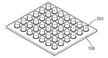
하부 반도체 패키지(100)를 구성하는 회로 기판(106)의 제1 전극 패드(108) 상에 도전성 접착층(202) 및 금속핀(204)이 형성되어 있다. 도전성 접착층(202)은 솔더 페이스트(solder paste)를 이용하여 형성할 수 있다. 금속핀(204)은 구리층으로 형성할 수 있다. 금속핀(204)은 금속 포스트(post)로 명명될 수 있다. 금속핀(204)은 도전성 접착층(202)을 이용하여 회로 기판(206)의 제1 전극 패드(108) 상에 부착 및 고정되도록 형성할 수 있다.The conductive
금속핀(204)은 외부 고정 장치인 지그(jig)를 이용하여 제1 전극 패드(108) 상에 부착 및 고정되도록 형성할 수 있다. 지그를 이용할 경우, 적층되는 상부 반도체 패키지(300)의 외부 연결 단자들(320)의 미세한 피치(P1)와 동일한 피치(P1)를 갖는 금속핀들(204)을 형성할 수 있다. 다시 말해, 본 발명은 상부 반도체 패키지의 외부 연결 단자들(320)의 피치(P1)가 0.4mm이하, 특히 0.1 내지 0.3mm로 미세할 경우에도 금속핀들(204)의 피치도 이에 맞추어 대응할 수 있다. 금속핀들(204)은 제1 전극 패드들(108)의 배열과 동일하게 형성할 수 있다. 금속핀들(204)은 하부 반도체 패키지(100)를 구성하는 반도체 칩(112)의 높이보다 더 높게 형성할 수 있다. 금속핀들(204)의 측면 프로파일은 회로 기판(106) 상에서 수직하게 형성할 수 있다. 지그를 이용하여 금속핀들(204)을 제1 전극 패드들(108)에 부착 및 고정되도록 형성하는 방법에 대하여는 후에 보다 더 자세하게 설명한다.The
하부 반도체 패키지(100) 상에는 앞서 설명한 금속핀들(204)을 매개로 상부 반도체 패키지(300)가 수직방향으로 적층되어 있다. 상부 반도체 패키지(300)의 외부 연결 단자들(320)이 금속핀들(204)과 연결되어 하부 반도체 패키지(100)와 전기적으로 연결될 수 있다. 외부 연결 단자들(320) 및 금속핀들(204)의 피치(P1)는 동일하게 할 수 있다. 상부 반도체 패키지(300)는 멀티칩 패키지(multi chip package)일 수 있다.The
상부 반도체 패키지(300)를 보다 자세히 설명하면, 상부 반도체 패키지(300)는 하부 반도체 패키지(100)와 마찬가지로 코아층(302), 포토솔더레지스트층(304)을 갖는 회로 기판(306)을 포함한다. 회로 기판(306)의 일측 상면에는 포토솔더레지스트층(304)에 의해 절연된 제3 전극 패드(308)가 형성되어 있다. 도 1에서는 편의상 제3 전극 패드(308)를 하나만 도시하였다. 회로 기판(306) 상에는 접착층을 개재하여 복수개의 반도체 칩(312, 314)이 형성되어 있다.In more detail, the
반도체 칩(312, 314)은 와이어(316)를 이용하여 제3 전극 패드(308)와 연결된다. 반도체 칩(312, 314), 및 와이어(316)가 형성된 회로 기판(306) 상에는 봉지층(318)이 형성되어 있다. 회로 기판(306)의 일측 하면에는 포토솔더레지스트층(304)에 의해 절연된 복수개의 제4 전극 패드들(310)이 형성되어 있다. 제4 전극 패드(310) 상에는 외부 연결 단자(320)가 형성되어 있다. 앞서 설명한 바와 같이 외부 연결 단자(320)는 금속핀(204)에 적층되어 하부 반도체 패키지(100)와 전기적으로 연결된다. 외부 연결 단자(320)는 솔더볼로 구성한다.The semiconductor chips 312 and 314 are connected to the
이상과 같은 본 발명의 적층형 반도체 패키지(500a)는 하부 반도체 패키지(100)를 구성하는 회로 기판(106) 상에 지그를 이용하여 미세한 피치를 갖는 금속핀들(204)을 형성한다. 이렇게 할 경우, 본 발명은 미세한 피치(좁은 피치, P1)를 갖는 외부 연결 단자들(320)을 포함하는 상부 반도체 패키지(300)를 하부 반도체 패키지(100) 상에 용이하게 적층할 수 있다.The stacked
본 발명은 미세한 피치를 갖는 외부 연결 단자들(320)을 포함하는 상부 반도체 패키지(300)에 맞추어 하부 반도체 패키지(100)에 미세한 피치(P1)를 갖는 금속핀(204)을 형성할 수 있기 때문에 전체적으로 적층형 반도체 패키지(500a)의 크기를 줄일 수 있다. 또한, 본 발명은 미세한 피치(P1)를 갖고 많은 수의 외부 연결 단자들(320)을 포함하는 상부 반도체 패키지(300)라도 이에 대응하여 하부 반도체 패키지(100)에 미세한 피치(P1)를 갖는 많은 수의 금속핀들(204)을 형성하여 적층형 반도체 패키지(500a)를 완성할 수 있다.
According to the present invention, the
제2 실시예에 의해 제조된 적층형 반도체 패키지The stacked semiconductor package manufactured by the second embodiment
도 2는 본 발명의 제2 실시예에 의해 제조된 적층형 반도체 패키지를 도시한 단면도이다.2 is a cross-sectional view illustrating a stacked semiconductor package manufactured according to a second embodiment of the present invention.
구체적으로, 본 발명의 제2 실시예에 의해 제조된 적층형 반도체 패키지(500b)는 회로 기판(106) 상에 봉지층(130)을 더 형성하고, 언더필층(underfill layer, 116)을 형성하지 않는 것을 제외하고는 제1 실시예의 적층형 반도체 패키지(500a)와 구조 및 효과면에서 동일하다.Specifically, the stacked
본 발명의 제2 실시예에 의해 제조된 적층형 반도체 패키지(500b)는 금속핀들(204)의 상단면은 노출하면서 회로 기판(106), 반도체 칩(112) 및 금속핀들(204)을 몰딩하는 봉지층(130)을 형성한다. 다시 말해, 반도체 칩(112) 및 금속핀들(204)이 형성된 회로 기판(106)의 전면을 전체적으로 몰딩하는 봉지층(130)을 형성한다.The stacked
이렇게 되면, 금속핀들(204)이 봉지층(130)에 의해 보다 더 잘 고정된다. 봉지층(130)에 의해 잘 고정된 금속핀들(204) 상에 외부 연결 단자(320)를 갖는 상부 반도체 패키지(300)가 적층되어 적층형 반도체 패키지(500b)가 완성된다.
In this case, the metal pins 204 are better fixed by the
제3 실시예에 의해 제조된 적층형 반도체 패키지The stacked semiconductor package manufactured by the third embodiment
도 3은 본 발명의 제3 실시예에 의해 제조된 적층형 반도체 패키지를 도시한 단면도이다.3 is a cross-sectional view illustrating a stacked semiconductor package manufactured according to a third embodiment of the present invention.
구체적으로, 본 발명의 제3 실시예에 의해 제조된 적층형 반도체 패키지(500c)는 반도체 칩(112)을 회로 기판(106) 상에 와이어(142)로 연결하는 것을 제외하고는 제2 실시예의 적층형 반도체 패키지(500b)와 구조 및 효과면에서 동일하다.Specifically, the stacked
본 발명의 제3 실시예에 의해 제조된 적층형 반도체 패키지(500c)는 회로 기판(106) 상에 접착층을 개재하여 반도체 칩(112)을 탑재하고, 반도체 칩(112)은 와이어 본딩 방식을 이용하여 와이어(140)로 회로 기판(106)과 전기적으로 연결한다. 본 발명은 회로 기판(106) 상에 제1 및 제2 실시예의 플립칩 방식이 아닌 와이어 본딩(wire bonding) 방식으로 반도체 칩(112)을 회로 기판(106)과 전기적으로 연결한다.The stacked
회로 기판(106)에는 금속핀들(204) 및 봉지층(130)이 형성된 후, 봉지층(130)에 의해 잘 고정된 금속핀들(104) 상에 제2 외부 연결 단자(32)를 갖는 상부 반도체 패키지(300)가 적층되어 적층형 반도체 패키지(500c)가 완성된다.
After forming the metal pins 204 and the
다음에는, 도 1 내지 도 3의 적층형 반도체 패키지(500a, 500b, 500c)에 이용될 수 있는 금속핀(204)의 구조를 보다 더 자세하게 설명한다.Next, the structure of the
도 4 및 도 5는 도 1 내지 도 3의 금속핀을 확대하여 도시한 도면이다.4 and 5 are enlarged views of the metal pins of FIGS. 1 to 3.
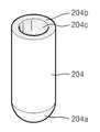
구체적으로, 도 4 및 도 5에 도시한 바와 같이 금속핀(204)의 하부, 즉 전극 패드(108)와 연결되는 부분에는 도금층(204a)을 형성할 수 있다. 도금층(204a)은 주석(Sn)층이나 주석합금층으로 형성할 수 있다. 도금층(204a)으로 인하여 하부 반도체 패키지(100)의 전극 패드(108)와 접착력을 크게 향상시킬 수 있다.Specifically, as shown in FIGS. 4 and 5, the
상부 반도체 패키지(300)와 연결되는 금속핀(204)의 상단부(204b)는 도 4에 도시한 바와 같이 평탄면을 갖게 형성할 수 있다. 또한, 상부 반도체 패키지(300)와 연결되는 금속핀(204)의 상단부(204b)는 도 5에 도시한 바와 같이 중앙 부분에 홈(204c)을 형성할 수 있다. 홈(204c)을 형성할 경우에는, 외부 연결 단자(320)가 보다 더 잘 안착되어 상부 반도체 패키지(300) 및 하부 반도체 패키지(100)를 전기적으로 잘 연결할 수 있다.An
또한, 상부 반도체 패키지(300)와 연결되는 금속핀(204)의 상단부(204b)에는 OSP(Organic Solderability Preservative) 표면 처리를 수행할 수 있다. OSP 처리는 적층형 반도체 패키지 제조시에 금속핀(204), 즉 구리층의 산화를 방지하기 위하여 수행할 수 있다.
In addition, an
비교예의 적층형 반도체 패키지Comparative Stacked Semiconductor Packages
도 6 및 도 7은 본 발명에 의해 제조된 적층형 반도체 패키지와 비교를 위한 비교예의 반도체 패키지를 도시한 단면도이다.6 and 7 are cross-sectional views showing a semiconductor package of a comparative example for comparison with a stacked semiconductor package manufactured by the present invention.
구체적으로, 도 6 및 도 7에서, 편의를 위하여 도 1 내지 도 3과 동일한 참조번호는 동일한 부재를 나타낸다. 도 6에 도시한 비교예의 적층형 반도체 패키지(600a)는 하부 반도체 패키지(100)에 봉지층(130a)을 형성하는 몰딩 공정에서 비아홀(132a)을 형성한다. 즉, 비교예의 적층형 반도체 패키지(600a)는 전극 패드(108) 영역을 제외하고 반도체 칩(112)을 포함하는 전체 영역 상에 봉지층(130a)을 형성한다. 비아홀(132a)에 하부 반도체 패키지(100)의 외부 연결 단자(142)를 형성한 후, 하부 반도체 패키지(100)의 외부 연결 단자(142) 상에 상부 반도체 패키지(300)의 외부 연결 단자(332)를 적층함으로써 적층형 반도체 패키지(600a)를 완성한다.Specifically, in Figs. 6 and 7, the same reference numerals as in Figs. 1 to 3 denote the same members for convenience. In the stacked
그리고, 도 7에 도시한 비교예의 적층형 반도체 패키지(600b)는 반도체 칩(112)이 형성된 회로 기판(106)의 전면에 전체적으로 봉지층(130b)을 형성한 후, 하부 반도체 패키지(100)의 봉지층(130b)을 레이저로 제거하여 비아홀(132b)을 형성한다. 그리고, 비아홀(132b)에 외부 연결 단자(144)를 형성한 후, 하부 반도체 패키지(100)의 외부 연결 단자(144) 상에 상부 반도체 패키지(300)의 외부 연결 단자(334)를 적층함으로써 적층형 반도체 패키지(600b)를 완성한다.In the stacked
비교예의 적층형 반도체 패키지들(600a, 600b)은 봉지층(130a, 130b)이 갖는 높이(h) 때문에 상부 반도체 패키지(300)의 외부 연결 단자(332, 334), 즉 솔더볼의 크기가 일정 이상이 되어야 하부 반도체 패키지(100) 및 상부 반도체 패키지(300)를 적층할 수 있다. 따라서, 비교예의 적층형 반도체 패키지(600a, 600b)는 외부 연결 단자(332, 334)의 크기를 줄이기가 어렵다.The
또한, 비교예의 적층형 반도체 패키지들(600a, 600b)은 비아홀(132a, 132b)의 높이보다 하부 반도체 패키지(100)의 외부 연결 단자(142, 144), 즉 솔더볼의 높이가 낮기 때문에, 상부 반도체 패키지(300)의 외부 연결 단자(332, 334)의 크기가 일정 이상이 되어야 하부 반도체 패키지(100) 및 상부 반도체 패키지(300)를 적층할 수 있다. 따라서, 비교예의 적층형 반도체 패키지(600a, 600b)는 외부 연결 단자(332, 334)의 크기나 피치를 줄이기가 어렵다. 예컨대, 도 7의 비교예의 적층형 반도체 패키지(600b)의 상하부 반도체 패키지들(100, 300)의 외부 연결 단자들(144, 344)의 피치(P2)는 0.4mm보다 커야 한다.In addition, the
이하에서는, 도 1 내지 도 5에서 설명한 바와 같은 본 발명에 의한 적층형 반도체 패키지의 제조 방법을 설명한다. 도 1 내지 도 5에서 설명한 내용이 제조 방법에도 바로 적용될 수 있다.
Hereinafter, a method of manufacturing a stacked semiconductor package according to the present invention as described with reference to FIGS. 1 to 5 will be described. 1 to 5 can be directly applied to the manufacturing method.
제1 실시예에 의한 적층형 반도체 패키지의 제조방법Method for manufacturing stacked semiconductor package according to the first embodiment
도 8 내지 도 10은 본 발명의 제1 실시예에 의한 적층형 반도체 패키지의 제조방법을 설명하기 위하여 도시한 단면도들이고, 도 11은 도 8 내지 도 10의 본 발명의 제1 실시예에 의한 적층형 반도체 패키지의 제조방법을 설명하기 위하여 도시한 흐름도이다.8 to 10 are cross-sectional views illustrating a method of manufacturing a stacked semiconductor package according to a first embodiment of the present invention, and FIG. 11 is a stacked semiconductor according to the first embodiment of the present invention of FIGS. 8 to 10. A flowchart illustrating a method of manufacturing a package is shown.
도 8 및 도 11을 참조하면, 코아층(102), 포토솔더레지스트층(104), 제1 및 제2 전극 패드들(108, 110)을 갖는 회로 기판(106)을 준비한다. 회로 기판(106) 상에 칩 연결 단자(114)를 갖는 반도체 칩(112)을 플립칩(flip chip) 방식으로 탑재한다(스텝 402). 다시 말해, 회로 기판(106) 상에 플립칩 어태치 공정으로 반도체 칩을 탑재한다. 플립칩 방식은 반도체 칩(112)의 액티브면을 아래로 하여 회로 기판(106) 상에 반도체 기판을 탑재하는 것이다.8 and 11, a
도 8에서는 편의상 하나의 단위 반도체 칩(112)이 회로 기판(106) 상에 탑재되는 것으로만 도시되어 있으나, 회로 기판(106) 상에는 여러 개의 반도체 칩들(112)이 탑재되어 있다. 플립칩 방식으로 형성된 반도체 칩(112) 하부의 회로 기판(106) 상에는 언더필층(116)을 형성한다(스텝 403). 언더필층(116)은 앞서 설명한 바와 같이 칩 연결 단자(114)를 보호하면서 반도체 칩(112)을 회로 기판(106) 상에 용이하게 고정하기 위하여 형성한다. 반도체 칩(112)은 회로 기판(106) 상에서 칩 연결 단자(114)를 통해 전극 패드(108)와 전기적으로 연결될 수 있다. 이와 같이 회로 기판(106), 제1 및 제2 전극 패드들(108, 110), 반도체 칩(112), 칩 연결 단자(114), 외부 연결 단자(118)를 포함하여 하부 반도체 패키지(100)가 완성된다.In FIG. 8, only one
도 9 및 도 11을 참조하면, 하부 반도체 패키지(100)를 구성하는 회로 기판(106)의 제1 전극 패드(108) 상에 도전성 접착층(202)을 매개로 금속핀(204)을 형성한다(스텝 404). 도전성 접착층(202)은 솔더 페이스트(solder paste)를 이용하여 형성한다. 금속핀(204)은 구리층으로 형성한다. 금속핀(204)은 도전성 접착층(202)을 이용하여 회로 기판(206)의 제1 전극 패드(108) 상에 부착 및 고정되도록 형성한다. 금속핀(204)의 측면 프로파일은 회로 기판(106) 상에서 수직하게 형성한다.9 and 11, a
금속핀(204)은 외부 고정 장치인 지그(jig)를 이용하여 제1 전극 패드(108) 상에 부착 및 고정되도록 형성한다. 외부 고정 장치인 지그를 이용할 경우, 앞서 설명한 바와 같이 적층되는 상부 반도체 패키지(300)의 외부 연결 단자들(320)의 미세한 피치에 대응하도록 금속핀들(204)을 형성할 수 있다. 금속핀들(204)을 제1 전극 패드들(108)의 배열과 동일하게 형성할 수 있다. 지그를 이용한 금속핀들(204)의 형성 방법에 대하여는 후에 보다 더 자세하게 설명한다.The
도 10 및 도 11을 참조하면, 전극 패드들(108, 110) 및 금속핀(204)이 형성된 회로 기판(106)에 백엔드 공정을 실시한다(스텝 408). 백엔드 공정은 단위 반도체 칩별로 회로 기판(106)을 절단하는 싱큘레이션(singulation) 공정을 실시하고, 회로 기판(106)의 하부에 외부 연결 단자(118)를 형성하는 공정이다. 이어서, 앞서 설명한 바와 같은 상부 반도체 패키지(300)를 준비한다. 계속하여, 하부 반도체 패키지(100) 상에 금속핀들을 매개로 외부 연결 단자(320)를 갖는 상부 반도체 패키지(300)를 수직 방향으로 적층하여 전기적으로 연결한다(스텝 410). 이렇게 하면 앞서 설명한 적층형 반도체 패키지(500a)가 완성된다.
10 and 11, a back end process is performed on a
제2 실시예에 의한 적층형 반도체 패키지의 제조방법Method for manufacturing stacked semiconductor package according to the second embodiment
도 12 내지 도 15는 본 발명의 제2 실시예에 의한 적층형 반도체 패키지의 제조방법을 설명하기 위하여 도시한 단면도들이고, 도 16은 도 12 내지 도 15의 본 발명의 제2 실시예에 의한 적층형 반도체 패키지의 제조방법을 설명하기 위하여 도시한 흐름도이다.12 to 15 are cross-sectional views illustrating a method of manufacturing a stacked semiconductor package according to a second embodiment of the present invention, and FIG. 16 is a stacked semiconductor according to a second embodiment of the present invention of FIGS. 12 to 15. A flowchart illustrating a method of manufacturing a package is shown.
도 12 및 도 16을 참조하면, 앞서 설명한 바와 같이 회로 기판(106) 상에 칩 연결 단자(114)를 갖는 반도체 칩(112)을 플립칩(flip chip) 방식으로 탑재한다(스텝 402). 도 12에서도 앞서 도 8과 마찬가지로 하나의 단위 반도체 칩(112)이 탑재되는 것으로 도시되어 있으나, 회로 기판(106) 상에는 여러 개의 반도체 칩이 탑재되어 있다.12 and 16, the
도 13, 14 및 도 16을 참조하면, 앞서 설명한 바와 같이 하부 반도체 패키지(100)를 구성하는 회로 기판(106)의 제1 전극 패드(108) 상에 도전성 접착층(202)을 매개로 금속핀(204)을 형성한다(스텝 404). 계속하여, 금속핀(204)의 상단면은 노출하면서 회로 기판(106), 반도체 칩(112) 및 금속핀들(204)을 전체적으로 몰딩하는 봉지층(130)을 형성한다(스텝 406). 다시 말해, 반도체 칩(112) 및 금속핀들(204)이 형성된 회로 기판(106)의 전면을 몰딩하는 봉지층(130)을 형성한다. 이렇게 되면, 금속핀들(204)이 봉지층(130)에 의해 보다 더 잘 고정된다.13, 14, and 16, as described above, the metal pins 204 are formed on the
도 15 및 도 16을 참조하면, 앞서 설명한 바와 같이 전극 패드들(108, 110) 및 금속핀(204)이 형성된 회로 기판(106)에 백엔드 공정을 실시한다(스텝 408). 이어서, 앞서 설명한 바와 같이 하부 반도체 패키지(100) 상에 금속핀들을 매개로 준비된 상부 반도체 패키지(300)를 수직 방향으로 적층한다(스텝 410). 이렇게 하면 앞서 설명한 적층형 반도체 패키지(500b)가 완성된다.15 and 16, as described above, the back end process is performed on the
이하에서는 도 1 내지 도 3의 적층형 반도체 패키지(500a, 500b, 500c)에 이용될 수 있는 금속핀(204)의 형성 방법을 설명한다. 금속핀(204)은 외부 고정 장치인 지를 이용하여 형성될 수 있다.Hereinafter, a method of forming the
도 17 내지 도 22는 본 발명에 적용되는 금속핀의 형성 방법을 개략적으로 설명하기 위한 도면들이다.17 to 22 are views for explaining a method of forming a metal pin to be applied to the present invention.
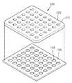
도 17을 참조하면, 도 17의 상측 도면에 도시한 바와 같이 지그(230)를 준비한다. 지그(230)는 금속판(220)과 금속판(220) 내에 홀들(221)을 구비한다. 홀들(221)은 회로 기판(106)의 전극 패드들(108)의 배열과 동일한 배열로 형성되어 있다. 도 17의 하측 도면은 회로 기판(106)에 전극 패드들(108)이 형성된 것을 예시적으로 도시한 것이고, 반도체 칩은 편의상 도시하지 않는다. 후술하는 바와 같이 회로 기판(106)의 전극 패드들(108)은 상부 반도체 패키지의 외부 연결 단자들의 피치와 동일하게 형성된다.Referring to FIG. 17, the
도 18을 참조하면, 지그(230)의 홀(221) 내에 금속핀(204)을 형성한다. 금속핀(204)은 구리층으로 형성할 수 있다. 금속핀(204)은 홀(221) 내에 정렬하여 형성한다. 금속핀(204)은 전극 패드들(108)의 배열과 동일한 배열로 형성한다. 금속핀(204)은 앞서 도 4 및 5에 도시한 바와 같은 구조를 갖는 것을 이용할 수 있다.Referring to FIG. 18, metal pins 204 are formed in
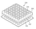
외부 고정 장치인 지그(230)의 홀(221) 내에 금속핀(204)을 형성하기 때문에, 금속핀들(204)의 피치에 구애받지 않고 금속핀(204)을 용이하게 형성할 수 있다. 회로 기판(106)의 전극 패드(108) 상에 도전성 접착층(202), 예컨대 솔더 페이스트를 형성한다.Since the
도 19 및 도 20을 참조하면, 도 19에 도시한 바와 같이 금속핀(204)이 형성된 지그(230)를 전극 패드(108) 및 도전성 접착층(202)이 형성된 회로 기판(106) 상에 적층한다. 즉, 회로 기판(106)의 전극 패드(108) 및 도전성 접착층(202)에 대응하여 금속핀(204)을 적층한다. 이어서, 지그(230)와 회로 기판(106)이 적층된 구조체를 리플로우 공정을 실시하여 도전성 접착층(202)을 리플로우 시킨다. 리플로우 공정은 지그(230)와 회로 기판(106)이 적층된 구조체를 리플로우 장비에서 적정 온도로 가열하여 도전성 접착층(202)을 용해시킨 후 냉각시키는 공정이다. 도전성 접착층(202)이 리플로우 공정을 거치게 되면, 금속핀((204)은 도전성 접착층(202) 상에 부착 및 고정된다.19 and 20, as illustrated in FIG. 19, a
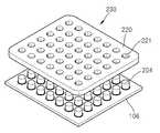
도 21 및 도 22를 참조하면, 지그(230)를 구성하는 금속판(220)을 분리한다. 이렇게 되면, 회로 기판(106) 상에 전극 패드(108)의 배열과 동일하게 배열되는 금속핀(204)이 형성된다. 필요에 따라서, 불필요한 도전성 접착층(202)을 제거하기 위한 디플러스 공정을 실시할 수 있다.21 and 22, the
이하에서는, 본 발명에 의한 적층형 반도체 패키지(500a, 500b, 500c)를 이용한 다양한 응용예를 설명한다. 응용예는 여러 가지가 있을 수 있지만 몇 가지만 설명한다. 도 23 내지 도 25에서는, 본 발명에 의한 적층형 반도체 패키지의 참조번호를 500으로만 표시한다.Hereinafter, various application examples using the stacked
도 23은 본 발명에 의한 칩 적층 패키지를 이용한 패키지 모듈의 구성을 도시한 개략도이다.Figure 23 is a schematic diagram showing the configuration of a package module using a chip stack package according to the present invention.
구체적으로, 본 발명에 의한 칩 적층 패키지(200, 500)는 패키지 모듈(600, package module)에 응용될 수 있다. 패키지 모듈(600)은 모듈 기판(610)에 적층형 반도체 패키지(500)가 복수개 부착되어 있다. 패키지 모듈(600)은 일측에 패키지(620)가 부착되어 있고, 타측에는 외부 접속 단자(630)가 위치한다. 본 발명에 의한 적층형 반도체 패키지(500)는 본 도면에 한정되지 않고 다양한 패키지 모듈에 적용될 수 있다.In detail, the chip stack packages 200 and 500 according to the present invention may be applied to a package module 600. The package module 600 has a plurality of stacked
도 24는 본 발명에 의한 적층형 반도체 패키지를 이용한 카드의 구성을 도시한 개략도이다.Fig. 24 is a schematic diagram showing the configuration of a card using the stacked semiconductor package according to the present invention.
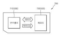
구체적으로, 본 발명에 의한 적층형 반도체 패키지(500)는 카드(700, card)에 응용될 수 있다. 카드(700)는 멀티 미디어 카드(Multimedia card, MMC), 보안 디지털 카드(Secure digital card, SD) 등을 포함한다. 카드(700)는 컨트롤러(710) 및 메모리(720)를 포함한다. 메모리(720)는 플래쉬 메모리, PRAM(phase change RAM(random access memory)) 또는 다른 형태의 비휘발성 메모리(non-volatile memory)일 수 있다. 컨트롤러(710)에서 메모리(720)로 제어 신호를 보내고, 컨트롤러(710)와 메모리(720)간에는 데이터를 주고받는다.Specifically, the stacked
본 발명의 카드(700)를 구성하는 컨트롤러(710) 및 메모리(720)를 앞서 설명한 바와 같은 본 발명의 적층형 반도체 패키지(500)로 채용할 수 있다. 이렇게 될 경우, 카드(700)는 메모리 용량을 크게 할 수 있고 다양한 기능을 갖는 컨트롤러(710)를 구비할 수 있다. 또한, 본 발명의 카드(700)는 두께를 얇게 할 수 있고, 배선 길이도 짧게 할 수 있어 성능을 향상시킬 수 있다.The
도 25는 본 발명에 의한 적층형 반도체 패키지를 이용한 전자 시스템의 구성을 도시한 개략도이다.25 is a schematic diagram showing the configuration of an electronic system using the stacked semiconductor package according to the present invention.
구체적으로, 본 발명에 의한 전자 시스템(800)은 컴퓨터, 모바일 폰(mobile phone), MP3(MPEG Audio Layer-3) 플레이어, 네비게이터(navigator) 등을 의미한다. 본 발명에 의한 전자 시스템(800)은 프로세서(810), 메모리(820), 입출력 장치(830)를 포함한다. 프로세서(810)와 메모리(820)나 입출력 장치(830)간에는 통신 채널(840, communication channel)을 이용하여 제어신호나 데이터를 주고받는다.Specifically, the
본 발명에 의한 전자 시스템(800)에서 적층형 반도체 패키지(500)를 프로세서(810) 및 메모리(820)에 채용된다. 이렇게 될 경우, 본 발명에 의한 전자 시스템(800)은 다양한 기능을 구현할 수 있고, 신뢰성도 향상시킬 수 있다.In the
500a, 500b, 500c, 600a, 600b: 반도체 패키지, 100: 하부 반도체 패키지, 300: 상부 반도체 패키지, 106, 306: 회로 기판, 108, 110, 308, 310: 전극 패드, 112, 312, 314: 반도체 칩, 114: 칩 연결 단자, 118, 320, 142, 332, 144, 344: 외부 연결 단자, 130, 130a, 130b: 봉지층, 132a, 132b: 비아홀, 140: 와이어, 202: 도전성 접착층, 204: 금속핀, 220: 금속판, 221: 홀, 230: 지그500a, 500b, 500c, 600a, 600b: semiconductor package, 100: lower semiconductor package, 300: upper semiconductor package, 106, 306: circuit board, 108, 110, 308, 310: electrode pad, 112, 312, 314: semiconductor Chip, 114: chip connection terminal, 118, 320, 142, 332, 144, 344: external connection terminal, 130, 130a, 130b: encapsulation layer, 132a, 132b: via hole, 140: wire, 202: conductive adhesive layer, 204: Metal pin, 220: metal plate, 221: hole, 230: jig
Claims (10)
Translated fromKorean상기 하부 반도체 패키지를 구성하는 상기 회로 기판의 전극 패드들 상에 복수개의 금속핀들을 부착 및 고정하고; 및
상기 하부 반도체 패키지 상에 상기 금속핀들을 매개로 상부 반도체 패키지를 수직 방향으로 적층하는 것을 특징으로 하는 적층형 반도체 패키지의 제조 방법.Preparing a lower semiconductor package including a semiconductor chip and a circuit board on which electrode pads are formed;
Attaching and fixing a plurality of metal pins on electrode pads of the circuit board constituting the lower semiconductor package; And
And stacking the upper semiconductor package in a vertical direction on the lower semiconductor package through the metal pins.
상기 회로 기판 상에 지그를 이용하여 상기 전극 패드들의 배열과 동일하게 배열되는 복수개의 금속핀들을 부착 및 고정하고; 및
상기 금속핀들과 전기적으로 연결되게 상부 반도체 패키지를 수직 방향으로 적층하는 것을 특징으로 하는 적층형 반도체 패키지의 제조방법.Preparing a lower semiconductor package including a circuit board to which a semiconductor chip is attached and a plurality of electrode pads are arranged on an upper surface of the semiconductor chip;
Attaching and fixing a plurality of metal pins arranged in the same manner as the arrangement of the electrode pads using a jig on the circuit board; And
And stacking the upper semiconductor package in a vertical direction so as to be electrically connected to the metal pins.
금속판과, 상기 금속판 내에 상기 회로 기판의 상기 전극 패드들의 배열과 동일한 배열로 형성된 복수개의 홀들을 포함하는 상기 지그를 준비하고,
상기 지그를 구성하는 상기 홀들 내에 상기 금속핀들을 위치시키고,
상기 지그 내에 포함된 상기 금속핀들을 상기 회로 기판의 전극 패드들 상에 부착 및 고정하고,
상기 금속판을 분리하여 이루어지는 것을 특징으로 하는 적층형 반도체 패키지의 제조방법.The method of claim 6, wherein the attachment and fixing of the metal pins,
Preparing a jig including a metal plate and a plurality of holes formed in the metal plate in the same arrangement as that of the electrode pads of the circuit board;
Place the metal pins in the holes constituting the jig,
Attaching and fixing the metal pins included in the jig on electrode pads of the circuit board,
The method of manufacturing a stacked semiconductor package, characterized in that the metal plate is separated.
상기 회로 기판의 전극 패드들 상에 도전성 접착층을 형성하고,
금속판과 상기 금속판 내에 상기 회로 기판의 상기 전극 패드들의 배열과 동일한 배열로 형성된 홀들을 구비하는 지그를 준비하고,
상기 지그의 홀들 내에 금속핀을 위치시키고,
상기 전극 패드들의 배열과 동일한 배열로 형성된 금속핀이 형성된 상기 지그를 상기 회로 기판의 전극 패드들 상에 형성된 상기 도전성 접착층 상에 적층하고,
상기 도전성 접착층을 리플로우하고,
상기 지그를 구성하는 금속핀을 분리하여 상기 회로 기판 상에 상기 전극 패드들의 배열과 동일하게 배열되는 복수개의 금속핀들을 형성하고, 및
상기 금속핀들과 전기적으로 연결되게 상부 반도체 패키지를 수직 방향으로 적층하는 것을 특징으로 하는 적층형 반도체 패키지의 제조 방법.Preparing a lower semiconductor package including a circuit board on which a semiconductor chip is attached and a plurality of electrode pads are arranged on an upper surface thereof;
Forming a conductive adhesive layer on the electrode pads of the circuit board,
Preparing a jig having a metal plate and holes formed in the metal plate in the same arrangement as that of the electrode pads of the circuit board;
Place the metal pin in the holes of the jig,
Stacking the jig on which the metal pins formed in the same arrangement as the array of the electrode pads are formed on the conductive adhesive layer formed on the electrode pads of the circuit board,
Reflow the conductive adhesive layer,
Separating a metal pin constituting the jig to form a plurality of metal pins arranged in the same manner as the array of the electrode pads on the circuit board, and
And stacking the upper semiconductor package in a vertical direction to be electrically connected to the metal pins.
Priority Applications (2)
| Application Number | Priority Date | Filing Date | Title |
|---|---|---|---|
| KR1020100068586AKR20120007839A (en) | 2010-07-15 | 2010-07-15 | Manufacturing method of stacked semiconductor package |
| US13/167,324US8785245B2 (en) | 2010-07-15 | 2011-06-23 | Method of manufacturing stack type semiconductor package |
Applications Claiming Priority (1)
| Application Number | Priority Date | Filing Date | Title |
|---|---|---|---|
| KR1020100068586AKR20120007839A (en) | 2010-07-15 | 2010-07-15 | Manufacturing method of stacked semiconductor package |
Publications (1)
| Publication Number | Publication Date |
|---|---|
| KR20120007839Atrue KR20120007839A (en) | 2012-01-25 |
Family
ID=45467310
Family Applications (1)
| Application Number | Title | Priority Date | Filing Date |
|---|---|---|---|
| KR1020100068586ACeasedKR20120007839A (en) | 2010-07-15 | 2010-07-15 | Manufacturing method of stacked semiconductor package |
Country Status (2)
| Country | Link |
|---|---|
| US (1) | US8785245B2 (en) |
| KR (1) | KR20120007839A (en) |
Cited By (2)
| Publication number | Priority date | Publication date | Assignee | Title |
|---|---|---|---|---|
| KR20170090772A (en)* | 2016-01-29 | 2017-08-08 | 삼성전기주식회사 | Printed circuit board, eletronic device package having the same |
| US20240260777A1 (en)* | 2021-06-14 | 2024-08-08 | Cuchen Co., Ltd | Cooking device |
Families Citing this family (56)
| Publication number | Priority date | Publication date | Assignee | Title |
|---|---|---|---|---|
| KR101313391B1 (en) | 2004-11-03 | 2013-10-01 | 테세라, 인코포레이티드 | Stacked packaging improvements |
| US8058101B2 (en) | 2005-12-23 | 2011-11-15 | Tessera, Inc. | Microelectronic packages and methods therefor |
| US8896126B2 (en) | 2011-08-23 | 2014-11-25 | Marvell World Trade Ltd. | Packaging DRAM and SOC in an IC package |
| US9941195B2 (en)* | 2009-11-10 | 2018-04-10 | Taiwan Semiconductor Manufacturing Co., Ltd. | Vertical metal insulator metal capacitor |
| US8482111B2 (en) | 2010-07-19 | 2013-07-09 | Tessera, Inc. | Stackable molded microelectronic packages |
| US9159708B2 (en) | 2010-07-19 | 2015-10-13 | Tessera, Inc. | Stackable molded microelectronic packages with area array unit connectors |
| KR101075241B1 (en) | 2010-11-15 | 2011-11-01 | 테세라, 인코포레이티드 | Microelectronic package with terminals in dielectric member |
| US20120146206A1 (en) | 2010-12-13 | 2012-06-14 | Tessera Research Llc | Pin attachment |
| US8618659B2 (en) | 2011-05-03 | 2013-12-31 | Tessera, Inc. | Package-on-package assembly with wire bonds to encapsulation surface |
| KR101128063B1 (en) | 2011-05-03 | 2012-04-23 | 테세라, 인코포레이티드 | Package-on-package assembly with wire bonds to encapsulation surface |
| EP2716142A1 (en)* | 2011-06-01 | 2014-04-09 | Telefonaktiebolaget LM Ericsson (PUBL) | Thermo/electrical conductor arrangement for multilayer printed circuit boards |
| US8836136B2 (en) | 2011-10-17 | 2014-09-16 | Invensas Corporation | Package-on-package assembly with wire bond vias |
| US8946757B2 (en) | 2012-02-17 | 2015-02-03 | Invensas Corporation | Heat spreading substrate with embedded interconnects |
| US8372741B1 (en) | 2012-02-24 | 2013-02-12 | Invensas Corporation | Method for package-on-package assembly with wire bonds to encapsulation surface |
| US9349706B2 (en) | 2012-02-24 | 2016-05-24 | Invensas Corporation | Method for package-on-package assembly with wire bonds to encapsulation surface |
| US8835228B2 (en) | 2012-05-22 | 2014-09-16 | Invensas Corporation | Substrate-less stackable package with wire-bond interconnect |
| US9391008B2 (en) | 2012-07-31 | 2016-07-12 | Invensas Corporation | Reconstituted wafer-level package DRAM |
| US9502390B2 (en) | 2012-08-03 | 2016-11-22 | Invensas Corporation | BVA interposer |
| US8642393B1 (en)* | 2012-08-08 | 2014-02-04 | Taiwan Semiconductor Manufacturing Company, Ltd. | Package on package devices and methods of forming same |
| CN103681365B (en)* | 2012-08-31 | 2016-08-10 | 宏启胜精密电子(秦皇岛)有限公司 | Package-on-package structure and preparation method thereof |
| US8975738B2 (en) | 2012-11-12 | 2015-03-10 | Invensas Corporation | Structure for microelectronic packaging with terminals on dielectric mass |
| US8878353B2 (en) | 2012-12-20 | 2014-11-04 | Invensas Corporation | Structure for microelectronic packaging with bond elements to encapsulation surface |
| US9136254B2 (en) | 2013-02-01 | 2015-09-15 | Invensas Corporation | Microelectronic package having wire bond vias and stiffening layer |
| US9034696B2 (en) | 2013-07-15 | 2015-05-19 | Invensas Corporation | Microelectronic assemblies having reinforcing collars on connectors extending through encapsulation |
| US8883563B1 (en) | 2013-07-15 | 2014-11-11 | Invensas Corporation | Fabrication of microelectronic assemblies having stack terminals coupled by connectors extending through encapsulation |
| US9023691B2 (en) | 2013-07-15 | 2015-05-05 | Invensas Corporation | Microelectronic assemblies with stack terminals coupled by connectors extending through encapsulation |
| US9167710B2 (en) | 2013-08-07 | 2015-10-20 | Invensas Corporation | Embedded packaging with preformed vias |
| US9685365B2 (en) | 2013-08-08 | 2017-06-20 | Invensas Corporation | Method of forming a wire bond having a free end |
| US20150076714A1 (en) | 2013-09-16 | 2015-03-19 | Invensas Corporation | Microelectronic element with bond elements to encapsulation surface |
| US9263394B2 (en) | 2013-11-22 | 2016-02-16 | Invensas Corporation | Multiple bond via arrays of different wire heights on a same substrate |
| US9583456B2 (en) | 2013-11-22 | 2017-02-28 | Invensas Corporation | Multiple bond via arrays of different wire heights on a same substrate |
| US9379074B2 (en) | 2013-11-22 | 2016-06-28 | Invensas Corporation | Die stacks with one or more bond via arrays of wire bond wires and with one or more arrays of bump interconnects |
| US9583411B2 (en) | 2014-01-17 | 2017-02-28 | Invensas Corporation | Fine pitch BVA using reconstituted wafer with area array accessible for testing |
| US10971476B2 (en) | 2014-02-18 | 2021-04-06 | Qualcomm Incorporated | Bottom package with metal post interconnections |
| TWI517343B (en)* | 2014-03-25 | 2016-01-11 | 恆勁科技股份有限公司 | Flip-chip package-on-package structure and its fabrication method |
| US9214454B2 (en) | 2014-03-31 | 2015-12-15 | Invensas Corporation | Batch process fabrication of package-on-package microelectronic assemblies |
| KR101565690B1 (en)* | 2014-04-10 | 2015-11-03 | 삼성전기주식회사 | Circuit board, method for menufacturing of circuit board, electronic component package and method for menufacturing of electronic component package |
| US9437577B2 (en)* | 2014-05-09 | 2016-09-06 | Mediatek Inc. | Package on package structure with pillar bump pins and related method thereof |
| US10381326B2 (en) | 2014-05-28 | 2019-08-13 | Invensas Corporation | Structure and method for integrated circuits packaging with increased density |
| US9646917B2 (en) | 2014-05-29 | 2017-05-09 | Invensas Corporation | Low CTE component with wire bond interconnects |
| US9412714B2 (en) | 2014-05-30 | 2016-08-09 | Invensas Corporation | Wire bond support structure and microelectronic package including wire bonds therefrom |
| US9735084B2 (en) | 2014-12-11 | 2017-08-15 | Invensas Corporation | Bond via array for thermal conductivity |
| US9888579B2 (en) | 2015-03-05 | 2018-02-06 | Invensas Corporation | Pressing of wire bond wire tips to provide bent-over tips |
| US9502372B1 (en) | 2015-04-30 | 2016-11-22 | Invensas Corporation | Wafer-level packaging using wire bond wires in place of a redistribution layer |
| US9761554B2 (en) | 2015-05-07 | 2017-09-12 | Invensas Corporation | Ball bonding metal wire bond wires to metal pads |
| US10490528B2 (en) | 2015-10-12 | 2019-11-26 | Invensas Corporation | Embedded wire bond wires |
| US9490222B1 (en) | 2015-10-12 | 2016-11-08 | Invensas Corporation | Wire bond wires for interference shielding |
| US10332854B2 (en) | 2015-10-23 | 2019-06-25 | Invensas Corporation | Anchoring structure of fine pitch bva |
| US10181457B2 (en) | 2015-10-26 | 2019-01-15 | Invensas Corporation | Microelectronic package for wafer-level chip scale packaging with fan-out |
| US10043779B2 (en) | 2015-11-17 | 2018-08-07 | Invensas Corporation | Packaged microelectronic device for a package-on-package device |
| US9659848B1 (en) | 2015-11-18 | 2017-05-23 | Invensas Corporation | Stiffened wires for offset BVA |
| US9984992B2 (en) | 2015-12-30 | 2018-05-29 | Invensas Corporation | Embedded wire bond wires for vertical integration with separate surface mount and wire bond mounting surfaces |
| US9935075B2 (en) | 2016-07-29 | 2018-04-03 | Invensas Corporation | Wire bonding method and apparatus for electromagnetic interference shielding |
| US10299368B2 (en) | 2016-12-21 | 2019-05-21 | Invensas Corporation | Surface integrated waveguides and circuit structures therefor |
| CN112309998B (en)* | 2019-07-30 | 2023-05-16 | 华为技术有限公司 | Packaging device, manufacturing method thereof and electronic equipment |
| US10834839B1 (en)* | 2019-08-27 | 2020-11-10 | International Business Machines Corporation | Barrier for hybrid socket movement reduction |
Family Cites Families (13)
| Publication number | Priority date | Publication date | Assignee | Title |
|---|---|---|---|---|
| KR100772103B1 (en) | 2005-11-04 | 2007-11-01 | 주식회사 하이닉스반도체 | Laminated package and its manufacturing method |
| JP2007287906A (en) | 2006-04-17 | 2007-11-01 | Elpida Memory Inc | Electrode, electrode manufacturing method, and semiconductor device including the electrode |
| US20080023805A1 (en)* | 2006-07-26 | 2008-01-31 | Texas Instruments Incorporated | Array-Processed Stacked Semiconductor Packages |
| TWI331388B (en)* | 2007-01-25 | 2010-10-01 | Advanced Semiconductor Eng | Package substrate, method of fabricating the same and chip package |
| JP5003260B2 (en) | 2007-04-13 | 2012-08-15 | 日本電気株式会社 | Semiconductor device and manufacturing method thereof |
| US8378231B2 (en)* | 2008-07-31 | 2013-02-19 | Ibiden Co., Ltd. | Semiconductor device and method for manufacturing the same |
| US20100044860A1 (en)* | 2008-08-21 | 2010-02-25 | Tessera Interconnect Materials, Inc. | Microelectronic substrate or element having conductive pads and metal posts joined thereto using bond layer |
| JP5185062B2 (en)* | 2008-10-21 | 2013-04-17 | パナソニック株式会社 | Multilayer semiconductor device and electronic device |
| KR20100132823A (en)* | 2009-06-10 | 2010-12-20 | 삼성전기주식회사 | Flip chip substrate and manufacturing method thereof |
| JP5500936B2 (en)* | 2009-10-06 | 2014-05-21 | イビデン株式会社 | Circuit board and semiconductor module |
| US8390108B2 (en)* | 2009-12-16 | 2013-03-05 | Stats Chippac Ltd. | Integrated circuit packaging system with stacking interconnect and method of manufacture thereof |
| JP2011176502A (en)* | 2010-02-23 | 2011-09-08 | Seiko Instruments Inc | Method of manufacturing package, piezoelectric vibrator, oscillator, electronic device, and radio-controlled timepiece |
| JP2012099648A (en)* | 2010-11-02 | 2012-05-24 | Fujitsu Semiconductor Ltd | Semiconductor device, and method of manufacturing the same |
- 2010
- 2010-07-15KRKR1020100068586Apatent/KR20120007839A/ennot_activeCeased
- 2011
- 2011-06-23USUS13/167,324patent/US8785245B2/enactiveActive
Cited By (2)
| Publication number | Priority date | Publication date | Assignee | Title |
|---|---|---|---|---|
| KR20170090772A (en)* | 2016-01-29 | 2017-08-08 | 삼성전기주식회사 | Printed circuit board, eletronic device package having the same |
| US20240260777A1 (en)* | 2021-06-14 | 2024-08-08 | Cuchen Co., Ltd | Cooking device |
Also Published As
| Publication number | Publication date |
|---|---|
| US8785245B2 (en) | 2014-07-22 |
| US20120015481A1 (en) | 2012-01-19 |
Similar Documents
| Publication | Publication Date | Title |
|---|---|---|
| KR20120007839A (en) | Manufacturing method of stacked semiconductor package | |
| US8952513B2 (en) | Stack type semiconductor package and method of fabricating the same | |
| KR101746731B1 (en) | Integrated circuit packaging stacking system with redistribution and method of manufacture thereof | |
| US8922005B2 (en) | Methods and apparatus for package on package devices with reversed stud bump through via interconnections | |
| KR101695846B1 (en) | Stacked semiconductor packages | |
| US20180342476A1 (en) | Semiconductor device assembly with surface-mount die support structures | |
| TWI601266B (en) | Semiconductor device structure and manufacturing method thereof | |
| TWI599009B (en) | Semiconductor chip package, semiconductor module, method of fabricating the semiconductor chip package and method of fabricating the semiconductor module | |
| KR20110105364A (en) | Integrated circuit package system having a package stack and a method of manufacturing the same | |
| JP2013162128A (en) | Package-on-package-type semiconductor package and method of fabricating the same | |
| KR20130024567A (en) | Semiconductor package having supporting plate and method of forming the same | |
| KR20110032522A (en) | Package on package type semiconductor package and manufacturing method thereof | |
| CN103715166A (en) | Apparatus and method for a component package | |
| KR20100108305A (en) | Integrated circuit packaging system with post type interconnector and method of manufacture thereof | |
| KR101677125B1 (en) | Pin grid interposer | |
| CN112151528B (en) | Semiconductor device comprising contact fingers on opposing surfaces | |
| US9105626B2 (en) | High-density package-on-package structure | |
| KR101238213B1 (en) | Stack semiconductor package and method of manufacturing the same | |
| KR20150129348A (en) | Package on package and method for manufacturing the same | |
| EP2849226B1 (en) | Semiconductor package | |
| KR100913171B1 (en) | Manufacturing method of stack package | |
| US11456279B2 (en) | Integrated electronic element module, semiconductor package, and method for fabricating the same | |
| KR20110130017A (en) | Multi-chip package and manufacturing method thereof | |
| KR100674411B1 (en) | Semiconductor Package Using Core Ball and Manufacturing Method Thereof | |
| KR102674312B1 (en) | Semiconductor package |
Legal Events
| Date | Code | Title | Description |
|---|---|---|---|
| PA0109 | Patent application | Patent event code:PA01091R01D Comment text:Patent Application Patent event date:20100715 | |
| PG1501 | Laying open of application | ||
| A201 | Request for examination | ||
| PA0201 | Request for examination | Patent event code:PA02012R01D Patent event date:20150610 Comment text:Request for Examination of Application Patent event code:PA02011R01I Patent event date:20100715 Comment text:Patent Application | |
| E902 | Notification of reason for refusal | ||
| PE0902 | Notice of grounds for rejection | Comment text:Notification of reason for refusal Patent event date:20160517 Patent event code:PE09021S01D | |
| E601 | Decision to refuse application | ||
| PE0601 | Decision on rejection of patent | Patent event date:20161110 Comment text:Decision to Refuse Application Patent event code:PE06012S01D Patent event date:20160517 Comment text:Notification of reason for refusal Patent event code:PE06011S01I |