KR20120007668A - Light emitting diode module - Google Patents
Light emitting diode moduleDownload PDFInfo
- Publication number
- KR20120007668A KR20120007668AKR1020100068312AKR20100068312AKR20120007668AKR 20120007668 AKR20120007668 AKR 20120007668AKR 1020100068312 AKR1020100068312 AKR 1020100068312AKR 20100068312 AKR20100068312 AKR 20100068312AKR 20120007668 AKR20120007668 AKR 20120007668A
- Authority
- KR
- South Korea
- Prior art keywords
- light emitting
- emitting diode
- housing
- light
- metal
- Prior art date
- Legal status (The legal status is an assumption and is not a legal conclusion. Google has not performed a legal analysis and makes no representation as to the accuracy of the status listed.)
- Granted
Links
Images


Classifications
- H—ELECTRICITY
- H10—SEMICONDUCTOR DEVICES; ELECTRIC SOLID-STATE DEVICES NOT OTHERWISE PROVIDED FOR
- H10H—INORGANIC LIGHT-EMITTING SEMICONDUCTOR DEVICES HAVING POTENTIAL BARRIERS
- H10H20/00—Individual inorganic light-emitting semiconductor devices having potential barriers, e.g. light-emitting diodes [LED]
- H10H20/80—Constructional details
- H10H20/85—Packages
- H10H20/858—Means for heat extraction or cooling
- H10H20/8582—Means for heat extraction or cooling characterised by their shape
- H—ELECTRICITY
- H10—SEMICONDUCTOR DEVICES; ELECTRIC SOLID-STATE DEVICES NOT OTHERWISE PROVIDED FOR
- H10H—INORGANIC LIGHT-EMITTING SEMICONDUCTOR DEVICES HAVING POTENTIAL BARRIERS
- H10H20/00—Individual inorganic light-emitting semiconductor devices having potential barriers, e.g. light-emitting diodes [LED]
- H10H20/80—Constructional details
- H10H20/85—Packages
- H10H20/8506—Containers
- H—ELECTRICITY
- H10—SEMICONDUCTOR DEVICES; ELECTRIC SOLID-STATE DEVICES NOT OTHERWISE PROVIDED FOR
- H10H—INORGANIC LIGHT-EMITTING SEMICONDUCTOR DEVICES HAVING POTENTIAL BARRIERS
- H10H20/00—Individual inorganic light-emitting semiconductor devices having potential barriers, e.g. light-emitting diodes [LED]
- H10H20/80—Constructional details
- H10H20/85—Packages
- H10H20/855—Optical field-shaping means, e.g. lenses
- H10H20/856—Reflecting means
Landscapes
- Arrangement Of Elements, Cooling, Sealing, Or The Like Of Lighting Devices (AREA)
Abstract
Translated fromKoreanDescription
Translated fromKorean본 발명은 발광다이오드 모듈에 관한 것으로서, 더욱 상세하게는 발광다이오드를 피시비(Printed Circuit Board) 상에 실장함으로써, 발광다이오드의 광출력 효율을 향상시키는 것은 물론 설치장소의 목적에 따라 발광다이오드 모듈의 갯 수를 패키지 형태로 결합하여 사용할 수 있는 제품경쟁력을 강화하는 발광다이오드 모듈에 관한 것이다.
The present invention relates to a light emitting diode module, and more particularly, by mounting a light emitting diode on a printed circuit board to improve the light output efficiency of the light emitting diode as well as the number of light emitting diode modules according to the purpose of the installation place. The present invention relates to a light emitting diode module for enhancing product competitiveness that can be used by combining numbers in a package form.
일반적으로 등기구의 광원으로는 백열등, 고압수은등, 형광등, 나트륨등과 같은 다양한 종류가 사용되나 밝기에 비하여 에너지 소비가 크고 수명이 짧다는 문제가 있다.In general, various kinds of light sources such as incandescent lamps, high pressure mercury lamps, fluorescent lamps and sodium lamps are used, but there is a problem in that energy consumption is large and life is shorter than brightness.
따라서 최근에는 상기와 같은 문제점을 해소하기 위하여 등기구의 광원으로 발광다이오드를 많이 사용하고 있는 추세이다.Therefore, in recent years, in order to solve the above problems, light emitting diodes are being used as a light source of a luminaire.
상기 발광다이오드는 LED(Light Emitting Diode)란 부르며, 이는 화합물 반도체의 특성을 이용해 전기 신호를 적외선, 가시광선 또는 빛의 형태로 변환시켜 신호를 보내고 받는 데 사용되는 발광소자이다.The light emitting diode is called an LED (Light Emitting Diode), which is a light emitting device used to send and receive signals by converting an electric signal into a form of infrared rays, visible rays, or light using characteristics of a compound semiconductor.
또한, 최근 각종 기계장치의 표시용 소자, 자동차의 외장에 들어가는 조명이나 내부의 기기, 전광판 등에 널리 사용되고 있다.In recent years, the present invention has been widely used for display devices of various mechanical devices, lighting used in exteriors of automobiles, internal devices, and electronic displays.
이러한, 발광다이오드를 광원으로 하는 발광다이오드 모듈은 통상적으로 피시비 기판 위에 상면으로부터 인입되어 이루어진 발광다이오드 칩 장착부와, 상기 발광다이오드 칩 장착부 주위에 경사지게 형성된 반사막과, 상기 발광다이오드 칩 장착부에 장착되는 발광다이오드 칩과, 상기 발광다이오드 칩과 반사막의 상부에는 방출되는 광원을 조사하도록 렌즈가 구비된 구성이다.Such a light emitting diode module using a light emitting diode as a light source is typically a light emitting diode chip mounting portion formed by drawing from an upper surface on a PCB substrate, a reflective film formed obliquely around the light emitting diode chip mounting portion, and a light emitting diode mounted on the light emitting diode chip mounting portion. A lens is disposed on the chip, the light emitting diode chip and the reflective film to irradiate the light source emitted.
상기와 같은 구조를 갖는 발광다이오드 모듈은 높은 출력의 광을 얻기 위하여 전류의 크기를 높일 경우에는 발광다이오드 내에서 높은 열이 발생하는데, 이때 발광다이오드 모듈은 열에 의하여 온도가 상승할 경우 저항이 매우 낮아져 광효율성이 저하되는 문제점이 있었다.The light emitting diode module having the above structure generates high heat in the light emitting diode when the current is increased in order to obtain high output light. In this case, the light emitting diode module has a very low resistance when the temperature increases due to heat. There was a problem that the light efficiency is lowered.
그러나, 종래의 발광다이오드가 사용되는 조명기구의 상기 발광다이오드가 실장된 발광다이오드 모듈 자체에는 방열기능을 탑재하고 있지 않기 때문에, 조명기구의 전체에 방열기능을 수행할 수 있는 방열수단을 구성함에 따라 각각의 발광다이오드 모듈에서 발생되는 열이 조명기구의 하나에서만 방열이 이루어져 결국, 발광다이오드의 방열효율이 떨어지는 문제점이 있었다.However, since the light emitting diode module itself in which the light emitting diode is mounted has no heat dissipation function, a heat dissipation means capable of performing a heat dissipation function in the entire lighting fixture is provided. Since heat generated from each light emitting diode module is radiated only by one of the lighting fixtures, there is a problem that the heat radiation efficiency of the light emitting diodes is lowered.
또한, 조명기구 전체에 방열수단을 구성함에 따라 디자인 표현의 한계성을 가지는 제품경쟁력을 떨어뜨리는 문제점이 있었다.
In addition, there is a problem in reducing the product competitiveness having a limit of design expression by configuring the heat radiating means in the entire lighting fixture.
상기와 같은 문제점을 해결하기 위해 제안하는 것으로서, 본 발명의 목적은 발광다이오드를 메탈피씨비에 장착하고 아울러, 상기 메탈피씨비의 양단에 히트싱크 및 커버를 구성하며 상기 메탈피씨비와 히트싱크 및 커버는 동일한 재질로 이루어져 열전도율을 향상시킴으로써 상기 발광다이오드에서 발생한 열이 상기 메탈피씨비를 통해 히트싱크 및 커버로의 열전도가 용이하게 이루어져, 동일한 체적상태에서 최적의 방열효율성을 발휘할 수 있도록 하는 제품 경쟁력을 강화하는 발광다이오드 모듈을 제공하는 데 있다.
In order to solve the above problems, an object of the present invention is to mount a light emitting diode to a metal PC, and to configure a heat sink and a cover at both ends of the metal PC, the metal PC and the heat sink and cover is the same It is made of a material to improve the thermal conductivity of the heat generated from the light emitting diode to the heat sink and the cover through the metal PC ratio is easily made, the light emission to enhance the product competitiveness to achieve the optimal heat dissipation efficiency in the same volume state To provide a diode module.
상기와 같은 목적을 달성하기 위한 본 발명은 발광다이오드를 광원으로 하는 발광다이오드 모듈에 있어서, 상기 발광다이오드 모듈은 중앙에 일정높이 세워지고 외주연에 제1수나사부가 형성된 돌출부와 상기 돌출부의 타단에 제1패킹이 안착되는 안착홈이 형성된 날개로 구성된 제1하우징과 상기 제1하우징의 제1수나사부에 나사결합되도록 일단 내측에 제1암나사공이 형성되고 내측에 수용공간이 형성되며 외주연에 외부공기가 소통되도록 공기통로를 가지도록 복수의 방열핀이 형성되며 타단 외주연에는 제2수나사부가 구성된 제2하우징으로 마련된 히트싱크부와; 상기 히트싱크부의 제1 및 제2하우징 사이에 고정되도록 하나 또는 하나 이상의 발광다이오드가 장착된 메탈피씨비부; 상기 제2하우징의 수용공간에 마련되어 상기 메탈피씨비부에서 발광되는 빛을 확장시키는 리플렉터; 상기 리플렉터의 일단에 마련되어 상기 리플렉터로 이물질이 침투되는 것을 방지하도록 외주연에 제2패킹이 마련되는 투광부; 및 상기 제2하우징의 제2수나사부에 일단이 나사체결되고 내측에 제2투과공이 형성되어 상기 제2하우징에 투광부가 고정되도록 하는 커버;로 구성되는 것을 특징으로 한다.The present invention for achieving the above object is a light emitting diode module having a light emitting diode as a light source, wherein the light emitting diode module is a predetermined height in the center and a first male screw portion formed on the outer periphery and the other end of the protrusion 1 A first female screw hole is formed inside the first housing and a receiving space is formed on the inner side so as to be screwed to the first housing of the first housing and the first housing of the first housing formed with a seating groove in which the packing is seated. A heat sink having a plurality of heat dissipation fins formed to have an air passage so as to communicate with each other, and a second housing having a second male screw portion formed at an outer circumference of the other end; A metal PC portion mounted with one or more light emitting diodes to be fixed between the first and second housings of the heat sink unit; A reflector provided in an accommodation space of the second housing to expand light emitted from the metal PC portion; A light transmitting part provided at one end of the reflector and provided with a second packing at an outer periphery to prevent foreign matter from penetrating into the reflector; And a cover having one end screwed into the second male threaded portion of the second housing and a second transmission hole formed therein to fix the light-transmitting portion to the second housing.
본 발명은 발광다이오드를 광원으로 하는 발광다이오드 모듈에 있어서, 상기 발광다이오드 모듈은 내측에 수용공간이 형성되고 상기 수용공간이 형성된 일단의 외주연에 제3수나사부가 형성되며 타단의 외주연에 외부공기가 소통되도록 공기통로를 가지도록 복수의 방열핀이 일체로 구성된 히트싱크부와; 상기 히트싱크부의 수용공간에 수용되고 하나 또는 하나 이상의 발광다이오드가 장착된 메탈피씨비부; 상기 메탈피씨비부의 상단에 마련되어 상기 메탈피씨비부로 이물질 침투나 손상을 방지하도록 구성된 투광부; 및 상기 히티싱크부의 제3수나사부와 나사결합되도록 일단 내측에 제3암나사부가 형성되고 타단 중앙에 발광다이오드에서 발광된 빛의 투과를 간섭하지않도록 제3투과공이 형성되며 상기 제3투과공의 끝단에는 상기 투광부의 일단을 밀착시켜 고정되도록 하는 지지단턱이 형성된 커버;로 구성되는 것을 특징으로 한다.The present invention provides a light emitting diode module using a light emitting diode as a light source, wherein the light emitting diode module has an accommodating space formed therein, and a third male screw portion is formed at an outer periphery of one end in which the accommodating space is formed, and external air is formed at the outer periphery of the other end. A heat sink unit in which a plurality of heat dissipation fins are integrally formed to have an air passage so as to communicate with each other; A metal PCB part accommodated in the accommodation space of the heat sink part and equipped with one or more light emitting diodes; A light transmitting part provided on an upper end of the metal PC part and configured to prevent foreign substances from penetrating or damaging the metal PC part; And a third female threaded portion formed inside the first threaded portion so as to be screwed with the third male threaded portion of the heat dissipating portion, and a third through hole is formed at the other end so as not to interfere with the transmission of the light emitted from the light emitting diode. It characterized in that the cover; formed with a support stepped jaw to be fixed in close contact with one end of the light transmitting portion.
본 발명에 있어서, 메탈피씨비부는 일단에 피씨비패턴이 형성된 베이스판과; 상기 베이스판에 일단에 밀착되고 제1투과공이 형성된 베이스링; 및 상기 베이스판의 패턴에 발광다이오드가 실장되며 상기 발광다이오드의 절연과 보호를 위한 절연층;으로 구성됨이 바람직하다.In the present invention, the metal PC portion is a base plate formed with a PCB pattern at one end; A base ring in close contact with the base plate and having a first through hole formed therein; And a light emitting diode mounted on a pattern of the base plate, and an insulating layer for insulating and protecting the light emitting diode.
본 발명에 있어서, 투광부는 평판 또는 볼록렌즈 중 어느 하나;이고, 상기 히트싱크부의 방열핀에는 외부공기가 소통되도록 하는 하나 또는 하나 이상의 기공;을 더 포함함이 바람직하다.
In the present invention, the light transmitting portion is any one of a flat plate or a convex lens; and the heat sink fin of the heat sink portion, one or more pores to allow external air to communicate; preferably further includes.
이상과 같이, 발광다이오드를 메탈피씨비에 장착하고 아울러, 상기 메탈피씨비의 양단에 히트싱크 및 커버를 구성하며 상기 메탈피씨비와 히트싱크 및 커버는 동일한 재질로 이루어져 열전도율을 향상시킴으로써 상기 발광다이오드에서 발생한 열이 상기 메탈피씨비를 통해 히트싱크 및 커버로의 열전도가 용이하게 이루어져, 동일한 체적상태에서 최적의 방열효율성을 발휘할 수 있도록 하는 제품 경쟁력을 강화하는 효과가 있다.
As described above, the light emitting diode is mounted on the metal PC, and the heat sink and the cover are formed at both ends of the metal PC, and the metal PC and the heat sink and the cover are made of the same material to improve thermal conductivity. Through the metal PC ratio, the heat conduction to the heat sink and the cover is easily performed, thereby enhancing the product competitiveness to exert the optimal heat dissipation efficiency in the same volume state.
도 1은 본 발명의 제1실시 예에 따른 발광다이오드 모듈의 분리 사시도.
도 2는 본 발명의 제1실시 예에 따른 발광다이오드 모듈의 단면도.
도 3은 본 발명의 제2실시 예에 따른 발광다이오드 모듈의 단면도.
도 4는 본 발명의 제3실시 예에 따른 발광다이오드의 분리 사시도.
도 5는 본 발명의 제3실시 예에 따른 발광다이오드의 단면도.1 is an exploded perspective view of a light emitting diode module according to a first embodiment of the present invention;
2 is a cross-sectional view of a light emitting diode module according to a first embodiment of the present invention.
3 is a cross-sectional view of a light emitting diode module according to a second embodiment of the present invention.
4 is an exploded perspective view of a light emitting diode according to a third embodiment of the present invention;
5 is a cross-sectional view of a light emitting diode according to a third embodiment of the present invention.
이하, 본 발명을 첨부된 도면을 참조하여 설명하면 다음과 같다.
Hereinafter, the present invention will be described with reference to the accompanying drawings.
(제1실시 예)(Embodiment 1)
도 1은 본 발명의 제1실시 예에 따른 발광다이오드 모듈의 분리 사시도이고, 도 2는 본 발명의 제1실시 예에 따른 발광다이오드 모듈의 단면도로서, 이를 참조한다.1 is an exploded perspective view of a light emitting diode module according to a first embodiment of the present invention, and FIG. 2 is a cross-sectional view of the light emitting diode module according to the first embodiment of the present invention.
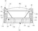
발광다이오드 모듈은 히트싱크부와, 상기 히트싱크부에 안착고정되고 발광다이오드를 광원으로 하여 빛을 발산하는 메탈피씨비부(20)와, 상기 메탈피씨비부(20)에 마련되어 빛을 확산시키도록 하는 리플렉터(30)와, 상기 리플렉턱(30)의 일단에 마련되는 투광부(40), 및 상기 투광부(40)를 고정시키도록 하는 커버(50)로 구성된다.The light emitting diode module is provided in the heat sink unit, the
상기 히트싱크부는 제1하우징(110)과, 상기 제1하우징(110)에 일단이 고정되는 제2하우징(120)으로 구성되며, 상기 제1 및 제2하우징(110)(120) 사이에는 메탈피씨비부(20)가 마련되어, 상호 고정에 의해 상기 메탈피씨비부(20)를 고정하게 되는 것이다.The heat sink unit includes a
따라서, 상기 히트싱크부는 발광다이오드를 광원으로 하는 메탈피씨비부(20)에서 발열하는 열을 방열시키는 역할뿐만 아니라 상기 발광다이오드를 보호하는 역할을 겸하는 수단이다.Accordingly, the heat sink unit serves to not only dissipate heat generated by the
상기 제1하우징(110)은 중앙에 일정높이를 가지는 돌출부(112)가 형성되고 그 외측에 상기 돌출부(112)보다 큰 지름을 가지는 날개(114)가 형성되며, 상기 돌출부(112)의 외주연에는 제1수나사부(113)가 형성되고, 상기 날개(114)와 돌출부(112) 사이에는 제1패킹(116)이 안착될 수 있는 안착홈(115)으로 구성된다.The
아울러, 상기 돌출부(112)의 어느 일측에는 하나 또는 하나 이상의 삽입공(118)이 형성되며, 상기 삽입공(118)은 메탈피씨비부(20)에서 연장되는 전원선 또는 기타 선들이 삽입되는 것으로, 경우에 따라서는 생략 가능하다.In addition, one side or one or
상기 제2하우징(120)은 일단 내측에 상기 제1하우징(110)의 돌출부(112) 제1수나사부(113)와 나사 체결되도록 제1암나사공(122)이 형성되고, 타단 내측에는 외부와 연통되는 수용공간(124)이 형성되며, 상기 제1암나사공(122)과 수용공간(124) 사이에는 메탈피씨비부(20)의 일단이 걸림되어 압박되도록 하는 단턱(123)으로 구성된다.The
아울러, 상기 제2하우징(120)의 일단 외주연에는 제2수나사부(126)가 형성되며, 타단에는 일정간격을 가지며 돌출되는 복수의 방열핀(128)이 형성되고 상기 복수의 방열핀(128) 사이 공간에는 외부 공기가 출입할 수 있는 공기통로(127)가 형성된다.In addition, a second
또한, 상기 복수의 방열핀(128)에는 하나 또는 하나 이상의 기공(129)이 형성됨이 바람직한 것으로, 이는 상기 공기통로(127)뿐만 아니라 기공(129)에 의해 외부 공기와의 접촉면적을 극대화하여 방열효율성을 향상시키는 것이다.In addition, it is preferable that one or
따라서, 히트싱크부는 제1하우징(110)의 제1수나사부(113)와 제2하우징(120)의 제1암나사공(122)이 상호 체결됨에 따라 고정되며 아울러, 상기 제1 및 제2하우징(110)(120) 사이에 제1패킹(116)이 마련됨에 따라 제1 및 제2하우징(110)(120) 사이에 고정되는 메탈피씨비부(20)로 이물질 또는 기타 불순물이 침투되는 것을 방지하게 된다.Therefore, the heat sink unit is fixed as the first male threaded
상기 메탈피씨비부(20)는 하나 또는 하나 이상의 발광다이오드가 장착되어 빛이 발산되도록 하는 수단이다.The
상기 메탈피씨비부(20)는 베이스판(22)과, 상기 베이스판(22)의 일단에 마련되고 중앙에 제1투과공(25)이 형성된 베이스링(24)과, 상기 베이스링(24)의 제1투과공(25) 범위 안에 마련되며 상기 베이스판(22)에 장착되는 발광다이오드(26), 및 상기 베이스링(24)의 제1투과공(25)에 도포되어 상기 발광다이오드(26)를 절연시킴과 동시에 이를 보호하는 절연층(28)으로 구성된다.The
아울러, 상기 베이스판(22)에는 발광다이오드(26)를 장착하기 위해 피씨비패턴이 형성되어 있음이 바람직하다.In addition, the
상기 베이스링(24)의 제1투과공(25)의 내측면은 수직면을 가지도록 형성될 수 있으나, 상기 제1투과공(25)의 내측면은 내측으로 경사진 형상을 가짐이 바람직한 것으로, 이는 상기 제1투과공(25)의 경사면에 절연층(28)의 도포면적을 극대화하여, 절연층(28)의 밀착력을 향상시키고 또한, 베이스판(22)과 베이스링(24)의 상호 결합력을 증폭하도록 하는 것이다.The inner surface of the first through
이 경우, 베이스판(22)과 베이스링(24)은 절연층(28)의 접착력에 의해 상호 결합되도록 구성할 수 있고, 경우에 따라서는 별도의 체결수단을 더 구성하여, 상호 고정력을 증폭하도록 구성할 수 있는 것이다.In this case, the
한편, 상기 절연층(28)은 발광다이오드(26)에서 발산하는 빛을 간섭하지 않는 재질로 구성됨이 바람직하고, 이 경우 에폭시수지임이 바람직하나, 이에 한정하는 것은 아니며, 베이스판(22)에 장착된 발광다이오드(26)의 절연 및 빛 발산을 간섭하지 않는 재질이면 어느 것이든 사용 가능하다.On the other hand, the
상기 리플렉터(30)는 메탈피씨비부(20)의 일단에 마련되어 빛을 확산시키는 수단이다.The
상기 리플렉터(30)는 깔대기 형상으로 양단이 개방되도록 형성되며 상기 메탈피씨비부(20)에 마련되는 일단보다 타단이 넓은 면이 위치하도록 구성함이 바람직하다.The
아울러, 상기 리플렉터(30)는 제2하우징(120)의 수용공간(124)에 마련되는 것이다.In addition, the
상기 투광부(40)는 상기 리플렉터(30)의 일단에 마련되어 상기 리플렉터(30)의 개방부로 이물질 또는 기타 불순물이 침투되는 것을 방지하고 또한 메탈피씨부(20)에서 발산하는 빛을 간섭하지 않도록 투명임이 바람직하나, 경우에 따라서는 장식의 효과를 위해 반투명 또는 색체가 가미된 것을 사용할 수 있다.The light-transmitting
아울러, 상기 투광부(40)의 외주연에는 제2패킹(42)을 더 구성하여, 상기 투광부(40)를 고정할 때 고정력에 의해 상기 투광부(40)가 파손됨을 방지할 뿐만 아니라 틈새로 이물질 또는 기타 불순물이 침투되는 것을 방지하는 것이다.In addition, the outer periphery of the light-transmitting
상기 커버(50)는 일단 내측에 제2하우징(120)의 제2수나사부(126)에 체결되도록 하는 제2암나사공(52)이 형성되고, 타단 중앙에는 발광다이오드(26)에서 발산되는 빛을 간섭하지 않도록 마련되는 제2투과공(54)으로 구성된다.The
아울러, 상기 커버(50)의 제2투과공(54)과 제2암나사공(52)에는 단턱이 형성되어, 상기 단턱이 투광부(40)의 외주연을 압박시킴으로 상기 투광부(40)를 고정시키게 되는 것이다.In addition, a stepped portion is formed in the second through
한편, 상기 히트싱크부의 제1 및 제2하우징(110)(120)과, 메탈피씨비부(20)의 베이스판(22)과 베이스링(24), 및 커버(50)는 동일한 재질로 형성됨이 바람직하고, 이 경우 열전도율이 좋은 금속임이 바람직하고, 금속 중 알루미늄임이 더욱 바람직하다.Meanwhile, the first and
상기와 같은 본 발명의 발광다이오드 모듈의 조립상태를 살펴보면 다음과 같다.Looking at the assembly state of the light emitting diode module of the present invention as described above are as follows.
먼저, 히트싱크부의 제1하우징(110) 돌출부(112)의 일면에 메탈피씨비부(20)를 안착한다.First, the
이때, 상기 메탈피씨비부(20)에서 연장된 전선들, 가령, 전원공급선(+)(-) 또는 기타 전선들을 상기 제1하우징(110)에 형성된 삽입공(118)으로 삽입시켜 외부로 노출시킴으로서, 외부장치들에 연결할 수 있는 것이다.At this time, by inserting the wires extending from the
아울러, 상기 제1하우징(110)에는 제2하우징(120)이 고정되는 것으로, 상기 제1하우징(110)의 제1수나사부(113)와 제2하우징(120)의 제1암나사공(122)이 상호 체결됨에 따라 고정되고, 이때 상기 제2하우징(120)은 제1하우징(110)의 돌출부(112)에 마련된 메탈피씨비부(20)의 일단을 압박함에 따라 상기 메탈피씨비부(20)가 고정되는 것이다.In addition, the
이 경우, 상기 제1하우징(110)의 날개(114) 안착홈(115)에는 제1패킹(116)이 안착된 상태이므로, 상기 제2하우징(120)이 체결로 고정됨에 따라 상기 제1 및 제2하우징(110)(120) 사이 공간을 제1패킹(116)에 의해 밀폐시킴으로서, 이물질 또는 불순물 침투를 방지하게 되는 것이다.In this case, since the
한편, 상기 제1하우징(110)에 고정된 제2하우징(120)에는 수용공간(124)이 형성되고, 상기 수용공간(124)으로 리플렉터(30)를 안착한다.Meanwhile, an
또한, 상기 리플렉턱(30)의 일단에는 외주연에 제2패킹(42)이 마련된 투광부(40)가 안착되고, 상기 투광부(40)의 일단에 커버(50)가 제2하우징(120)에 체결 고정됨에 따라 상기 투광부(40)를 고정시키게 된다.In addition, one end of the
따라서, 상기와 같이 구성된 발광다이오드 모듈은 사용목적에 따라 그 모듈 갯수를 달리하여 설치함에 따라 다양한 등기구로 사용할 수 있는 것이다.Therefore, the light emitting diode module configured as described above can be used in various luminaires by varying the number of modules according to the purpose of use.
아울러, 제1및 제2하우징(110)(120)과 메탈피씨비부(20) 및 커버(50)가 동일한 재질로 형성됨에 따라 상기 메탈피씨비부(20)의 발광다이오드(26)에서 발열된 열은 메탈피씨비부(20)와 면 밀착된 제1 및 제2하우징(110)(120)에 전도되고, 이렇게 전도된 열은 제2하우징(120)에 형성된 복수의 방열핀(128) 사이에 공기통로(127)가 형성되어 외부 공기와 소통함에 따라 방열이 용이하게 이루어지며, 특히 방열핀(128)에는 복수의 기공(129)이 형성되어 수평적 공기통로(127)뿐만 아니라 수직적 기공(129)을 통해 외부공기와의 접촉시간을 증가시켜 방열요율성을 극대화하는 것이다.
In addition, as the first and
(제2실시 예)(Second Embodiment)
도 3은 본 발명의 제2실시 예에 따른 발광다이오드 모듈의 단면도로서, 이를 참조하고, 제1실시 예와 동일한 구성에 대해서는 동일한 참조부호를 사용하고, 이에 대한 상세한 설명은 생략한다.3 is a cross-sectional view of a light emitting diode module according to a second exemplary embodiment of the present invention. Referring to the same, the same reference numerals are used for the same components as those of the first exemplary embodiment, and a detailed description thereof will be omitted.
제2실시 예에 따른 발광다이오드 모듈 중 투광부는 볼록렌즈(40a)임이 바람직한 것으로, 이는 제1실시 예에 도시된 바와 같이 투광부(40)는 평판형으로 이는 단순히 발광다이오드(26)를 투과시키는 것이나, 제2실시 예의 볼록렌즈(40a)는 빛을 확장시켜 광범위한 범위에 빛을 조사하도록 하는 것이다.Among the light emitting diode modules according to the second embodiment, the light transmitting portion is preferably a
한편, 볼록렌즈(40a)는 유리 또는 폴리비닐재 중 어느 하나로 형성되고, 이 경우 유리재임이 더욱 바람직하다.
On the other hand, the
(제3실시 예)(Third Embodiment)
도 4는 본 발명의 제3실시 예에 따른 발광다이오드의 단면도이고, 도 5는 본 발명의 제3실시 예에 따른 발광다이오드의 단면도로서, 이를 참조하고, 제1 및 제2실시 예와 동일한 구성에 대해서는 동일한 참조부호를 사용하고 이에 대한 상세한 설명은 생략한다.4 is a cross-sectional view of a light emitting diode according to a third embodiment of the present invention, and FIG. 5 is a cross-sectional view of the light emitting diode according to a third embodiment of the present invention. The same reference numerals are used for the description thereof and detailed description thereof will be omitted.
제3실시 예의 발광다이오드 모듈은 히트싱트부(130)와, 상기 히트싱크부(130)에 마련되는 메탈피씨비부(20)와, 상기 메탈피씨비부(20)에 마련되는 투광부, 및 상기 투광부에 고정력을 제공하는 커버(510)로 구성된다.The light emitting diode module according to the third embodiment of the present invention includes a
상기 히트싱크부(130)는 일정높이 세워진 상단 중앙에 메탈피씨비부(20)가 안착 고정되도록 수용공간(132)과 외주연에 제3수나사부(134)가 형성되고, 하단부에 일정간격을 가지는 복수의 방열핀(136)이 마련되며, 상기 복수의 방열핀(136) 사이에는 외부공기가 출입할 수 있는 공기통로(137)로 구성된다.The
아울러, 상기 히트싱크부(130)의 어느 일측에는 하나 또는 하나 이상의 삽입공(138)이 형성되어, 메탈피씨비부(20)에서 연장되는 전원전선이나 기타 전선이 외부장치와 연결되도록 하는 것이다.In addition, one side or one or
더불어, 상기 복수의 방열핀(136)에는 하나 또는 하나 이상의 기공(139)을 더 형성하여, 공기통로(137)에 의해 수평적으로 공기가 출입하고 더불어 상기 기공(130)을 통해 수직적으로 공기가 출입함에 따라 방열핀(136)에 의한 방열효율성을 극대화하는 것이다.In addition, one or
한편, 수용공간(132)은 메탈피씨비부(20)의 용이한 안착과 고정력을 증폭하고, 특히 히트싱크부와 메탈피씨비부(20)의 접촉면적을 극대화하여, 상기 메탈피씨비부(20)에서 발생한 열이 히트싱크부 및 커버(510)로 빠르게 전도되도록 하기 위한 수단으로, 경우에 따라서는 생략 가능한 것이다.On the other hand, the receiving
상기 메탈피씨비부(20)는 다수의 발광다이오드(26)가 장착되는 것으로, 이는 제1실시 예와 동일하므로 설명은 생략한다.The
상기 투광부는 제2실시 예의 볼록렌즈(40a) 임이 바람직하나, 이에 한정하는 것은 아니며, 제1실시 예에 도시된 바와 같이 평판을 형성할 수 있는 것이다.Preferably, the light-transmitting portion is the
상기 커버(510)는 히트싱크부(130)의 제3수나사부(134)와 나사체결되도록 일단 내측에 제3암나사공(512)이 형성되고, 타단 중앙에 메탈피씨비부(20)에서 발산되는 빛을 간섭하지 않도록 제3투과공(514)이 형성된다.The
아울러, 상기 제3투과공(514)에는 투광부인 볼록렌즈(40a)의 외주연 일측을 지지하는 지지단턱(516)을 더 형성함이 바람직하다.In addition, it is preferable to further form a
한편, 상기 히트싱크부(130)와 메탈피씨비부(20) 및 커버(510)는 동일한 재질로 형성하고, 이 경우 열전도율이 우수한 금속재임이 바람직하고, 금속 중 알루미늄이 더욱 바람직하다.Meanwhile, the
상기와 같이 구성된 발광다이오드 모듈의 조립상태를 살펴보면 다음과 같다.Looking at the assembly state of the light emitting diode module configured as described above are as follows.
먼저, 히트싱크부(130)의 수용공간(132)에 메탈피씨비부(20)를 안착하며, 상기 메탈피씨비부(20)에서 연장된 전선들을 삽입공(138)으로 삽입시켜 외부 장치들과 연결되도록 한다.First, the
아울러, 상기 히트싱크부(130)에 안착된 메탈피씨비부(20)의 일단에 볼록렌즈(40a)를 안착하고, 그 일단에 커버(510)를 조립하며, 상기 커버(510)의 제3암나사공(512)과 히트싱크부(130)의 제3수나사부(134)를 상호 체결시킨다.In addition, the
한편, 커버(510)의 제3투과공(514)에는 지지단턱(516)이 마련되어, 상호 체결에 의해 상기 지지단턱(516)이 볼록렌즈(40a)의 외주연 일측을 압박하는 것이다.On the other hand, the third through
따라서, 히트싱크부(130)와 커버(510)의 상호 체결에 의한 압박으로 메탈피씨비부(20) 및 투광부가 압박되어 고정되는 것이다.Therefore, the metal
특히, 히트싱크부(510)와, 메탈피씨비부(20) 및 커버(510)는 동일한 재질로 형성됨에 따라 동일한 열전도율을 가지고 있으며, 또한 히트싱크부(130)의 수용공간(132)에 메탈피씨비부(20)가 안착되어 접착면적을 극대화함으로써, 결국 접착면적의 극대화 및 동일한 재질의 열전도율에 의해 열전도효율성을 극대화하는 것이다.In particular, the
특히, 제3실시 예의 히트싱크부(130)는 제1실시 예와 같이 히트싱크부가 제1 및 제2하우징(110)(120)으로 분리되어 있지 않으므로, 열전도성을 극대화할 수 있는 것이다.
In particular, since the
이상에서 설명한 것은 본 발명에 따른 발광다이오드 모듈을 실시하기 위한 하나의 실시 예에 불과한 것으로서, 본 발명은 상기한 실시 예에 한정되지 않고, 이하 특허청구범위에서 청구하는 본 발명의 요지를 벗어남이 없이 본 발명이 속하는 기술분야에서 통상의 지식을 가진 자라면 누구든지 다양한 변경 실시가 가능한 범위까지 본 발명의 기술적 정신이 있다고 할 것이다.
What has been described above is only one embodiment for implementing a light emitting diode module according to the present invention, the present invention is not limited to the above embodiment, without departing from the gist of the invention claimed in the claims below Anyone with ordinary knowledge in the technical field of the present invention will have the technical spirit of the present invention to the extent that various modifications can be made.
110, 120: 제1 및 제2하우징112: 돌출부
113: 제1수나사부114: 날개
116: 제1패킹118: 삽입공
122: 제1암나사공124: 수용공간
126: 제2수나사부127: 공기통로
128: 방열핀129: 기공
130: 히트싱크부132: 수용공간
134: 제3수나사부136: 방열핀
137: 공기통로138: 삽입공
139: 기공20: 메탈피씨비부
22: 베이스판24: 베이스링
26: 발광다이오드28: 절연층
30: 리플렉터40: 투광부
50, 510: 커버52: 제2암나사공
54, 514: 제2투과공512: 제3암나사공
516: 지지단턱110, 120: first and second housing 112: projection
113: first male thread 114: wings
116: first packing 118: insertion hole
122: first female threader 124: receiving space
126: second male thread 127: air passage
128: heat radiation fin 129: pore
130: heat sink 132: receiving space
134: third male thread 136: heat dissipation fin
137: air passage 138: insertion hole
139: Pore 20: Metal PC Part
22: base plate 24: base ring
26: light emitting diode 28: insulating layer
30: reflector 40: light transmitting part
50, 510: Cover 52: second female thread hole
54, 514: Second hole 512: Third female threader
516: support step
Claims (5)
Translated fromKorean상기 발광다이오드 모듈은 중앙에 일정높이 세워지고 외주연에 제1수나사부(113)가 형성된 돌출부(112)와 상기 돌출부(112)의 타단에 제1패킹(116)이 안착되는 안착홈(115)이 형성된 날개(114)로 구성된 제1하우징(110)과 상기 제1하우징(110)의 제1수나사부(113)에 나사결합되도록 일단 내측에 제1암나사공(122)이 형성되고 내측에 수용공간(124)이 형성되며 외주연에 외부공기가 소통되도록 공기통로(127)를 가지도록 복수의 방열핀(128)이 형성되며 타단 외주연에는 제2수나사부(126)가 구성된 제2하우징(120)으로 마련된 히트싱크부와;
상기 히트싱크부의 제1 및 제2하우징(110)(120) 사이에 고정되도록 하나 또는 하나 이상의 발광다이오드가 장착된 메탈피씨비부(20);
상기 제2하우징(120)의 수용공간(124)에 마련되어 상기 메탈피씨비부(20)에서 발광되는 빛을 확장시키는 리플렉터(30);
상기 리플렉터(30)의 일단에 마련되어 상기 리플렉터(30)로 이물질이 침투되는 것을 방지하도록 외주연에 제2패킹(42)이 마련되는 투광부(40); 및
상기 제2하우징(120)의 제2수나사부(126)에 일단이 나사체결되고 내측에 제2투과공(54)이 형성되어 상기 제2하우징(120)에 투광부(40)가 고정되도록 하는 커버(50);
로 구성되는 것을 특징으로 하는 발광다이오드 모듈.
In the light emitting diode module using a light emitting diode as a light source,
The light emitting diode module has a predetermined height at the center and a protrusion 112 having a first male thread portion 113 formed at an outer circumference thereof, and a seating groove 115 at which the first packing 116 is seated at the other end of the protrusion 112. The first female threaded hole 122 is formed on the inner side of the first housing 110 and the first male threaded portion 113 of the first housing 110. A second housing 120 having a space 124 is formed and a plurality of heat dissipation fins 128 are formed to have an air passage 127 to communicate external air on the outer circumference, and the second male screw portion 126 is formed on the outer circumference of the other end. A heat sink unit);
A metal PC part 20 having one or more light emitting diodes mounted thereon to be fixed between the first and second housings 110 and 120 of the heat sink unit;
A reflector 30 provided in the accommodation space 124 of the second housing 120 to expand the light emitted from the metal PC portion 20;
A light-transmitting portion 40 provided at one end of the reflector 30 and provided with a second packing 42 at an outer periphery to prevent foreign matter from penetrating into the reflector 30; And
One end is screwed into the second male screw portion 126 of the second housing 120 and a second through hole 54 is formed therein so that the light transmitting portion 40 is fixed to the second housing 120. Cover 50;
Light emitting diode module, characterized in that consisting of.
상기 발광다이오드 모듈은 내측에 수용공간(132)이 형성되고 상기 수용공간(132)이 형성된 일단의 외주연에 제3수나사부(134)가 형성되며 타단의 외주연에 외부공기가 소통되도록 공기통로(137)를 가지도록 복수의 방열핀(136)이 일체로 구성된 히트싱크부(130)와;
상기 히트싱크부(130)의 수용공간(132)에 수용되고 하나 또는 하나 이상의 발광다이오드가 장착된 메탈피씨비부(20);
상기 메탈피씨비부(20)의 상단에 마련되어 상기 메탈피씨비부(20)로 이물질 침투나 손상을 방지하도록 구성된 투광부(40); 및
상기 히티싱크부(130)의 제3수나사부(134)와 나사결합되도록 일단 내측에 제3암나사부(512)가 형성되고 타단 중앙에 발광다이오드에서 발광된 빛의 투과를 간섭하지않도록 제3투과공(514)이 형성되며 상기 제3투과공(514)의 끝단에는 상기 투광부(40)의 일단을 밀착시켜 고정되도록 하는 지지단턱(516)이 형성된 커버(510);
로 구성되는 것을 특징으로 하는 발광다이오드 모듈.
In the light emitting diode module using a light emitting diode as a light source,
The light emitting diode module has an accommodation space 132 formed therein, and a third male threaded portion 134 is formed on the outer circumference of one end where the accommodation space 132 is formed, and the air passage communicates external air on the outer circumference of the other end. A heat sink 130 in which a plurality of heat dissipation fins 136 are integrally formed to have 137;
A metal PC portion 20 accommodated in the accommodation space 132 of the heat sink 130 and equipped with one or more light emitting diodes;
A light transmitting part 40 provided on an upper end of the metal PC part 20 and configured to prevent foreign substances from penetrating or damaging the metal PC part 20; And
A third female thread part 512 is formed at an inner side so as to be screwed into the third male thread part 134 of the heat sink 30, and a third transmission is performed so as not to interfere with transmission of light emitted from the light emitting diode at the other end. A cover 510 having a ball 514 formed therein and having a support step 516 formed at the end of the third transmission hole 514 to be fixed by bringing one end of the light transmitting part 40 into close contact with the end;
Light emitting diode module, characterized in that consisting of.
상기 메탈피씨비부(20)는 일단에 피씨비패턴이 형성된 베이스판(22)과;
상기 베이스판(22)에 일단에 밀착되고 제1투과공(25)이 형성된 베이스링(24); 및
상기 베이스판(22)의 패턴에 발광다이오드(26)가 실장되며 상기 발광다이오드(26)의 절연과 보호를 위한 절연층(28);
으로 구성되는 것을 특징으로 하는 발광다이오드 모듈.
The method according to claim 1 or 2,
The metal PC portion 20 may include: a base plate 22 having a PCB pattern formed at one end thereof;
A base ring 24 in close contact with the base plate 22 and having a first through hole 25 formed therein; And
A light emitting diode 26 mounted on a pattern of the base plate 22 and an insulating layer 28 for insulating and protecting the light emitting diode 26;
Light emitting diode module, characterized in that consisting of.
상기 투광부(40)는 평판 또는 볼록렌즈(40a) 중 어느 하나;
인 것을 특징으로 하는 발광다이오드 모듈.
The method according to claim 1 or 2,
The light transmitting portion 40 is any one of a flat plate or a convex lens (40a);
Light emitting diode module, characterized in that.
상기 히트싱크부의 방열핀에는 외부공기가 소통되도록 하는 하나 또는 하나 이상의 기공;
을 더 포함하는 것을 특징으로 하는 발광다이오드 모듈.
The method according to claim 1 or 2,
One or more pores to allow external air to communicate with the heat sink fins of the heat sink;
Light emitting diode module further comprising.
Priority Applications (1)
| Application Number | Priority Date | Filing Date | Title |
|---|---|---|---|
| KR1020100068312AKR101194254B1 (en) | 2010-07-15 | 2010-07-15 | A Light-emitting diode module |
Applications Claiming Priority (1)
| Application Number | Priority Date | Filing Date | Title |
|---|---|---|---|
| KR1020100068312AKR101194254B1 (en) | 2010-07-15 | 2010-07-15 | A Light-emitting diode module |
Publications (2)
| Publication Number | Publication Date |
|---|---|
| KR20120007668Atrue KR20120007668A (en) | 2012-01-25 |
| KR101194254B1 KR101194254B1 (en) | 2012-11-12 |
Family
ID=45612907
Family Applications (1)
| Application Number | Title | Priority Date | Filing Date |
|---|---|---|---|
| KR1020100068312AExpired - Fee RelatedKR101194254B1 (en) | 2010-07-15 | 2010-07-15 | A Light-emitting diode module |
Country Status (1)
| Country | Link |
|---|---|
| KR (1) | KR101194254B1 (en) |
Cited By (4)
| Publication number | Priority date | Publication date | Assignee | Title |
|---|---|---|---|---|
| KR101322683B1 (en)* | 2012-06-21 | 2013-10-30 | 고인홍 | Led lamp |
| KR101428361B1 (en)* | 2013-02-07 | 2014-08-13 | 김민수 | Chamber illumination device |
| KR101420734B1 (en)* | 2012-03-06 | 2014-08-13 | 주식회사 헤파스 | Led lighting module and led lamp using the same |
| EP3572769A4 (en)* | 2018-02-27 | 2020-04-01 | Guangdong Oppo Mobile Telecommunications Corp., Ltd. | LASER PROJECTION MODULE, DEPTH CAMERA AND ELECTRONIC DEVICE |
Families Citing this family (1)
| Publication number | Priority date | Publication date | Assignee | Title |
|---|---|---|---|---|
| KR101580672B1 (en)* | 2014-09-02 | 2015-12-31 | 주식회사 이츠웰 | water proof and heat exchaging light emitting diode lighting module |
Family Cites Families (2)
| Publication number | Priority date | Publication date | Assignee | Title |
|---|---|---|---|---|
| KR200377622Y1 (en) | 2004-12-21 | 2005-03-14 | 김봉수 | Heat sink type LED Flood Light with stabilized power supply |
| KR100496525B1 (en) | 2005-03-23 | 2005-06-22 | 주식회사 누리플랜 | Led illumination lamp |
- 2010
- 2010-07-15KRKR1020100068312Apatent/KR101194254B1/ennot_activeExpired - Fee Related
Cited By (5)
| Publication number | Priority date | Publication date | Assignee | Title |
|---|---|---|---|---|
| KR101420734B1 (en)* | 2012-03-06 | 2014-08-13 | 주식회사 헤파스 | Led lighting module and led lamp using the same |
| KR101322683B1 (en)* | 2012-06-21 | 2013-10-30 | 고인홍 | Led lamp |
| KR101428361B1 (en)* | 2013-02-07 | 2014-08-13 | 김민수 | Chamber illumination device |
| EP3572769A4 (en)* | 2018-02-27 | 2020-04-01 | Guangdong Oppo Mobile Telecommunications Corp., Ltd. | LASER PROJECTION MODULE, DEPTH CAMERA AND ELECTRONIC DEVICE |
| US11525669B2 (en) | 2018-02-27 | 2022-12-13 | Guangdong Oppo Mobile Telecommunications Corp., Ltd. | Laser projection module, depth camera and electronic device |
Also Published As
| Publication number | Publication date |
|---|---|
| KR101194254B1 (en) | 2012-11-12 |
Similar Documents
| Publication | Publication Date | Title |
|---|---|---|
| JP5578361B2 (en) | Lamp with lamp and lighting equipment | |
| CN102466162B (en) | Lamp unit and lighting fixture | |
| JP5320609B2 (en) | Lamp apparatus and lighting apparatus | |
| KR101032415B1 (en) | Radial heat dissipation device and bulb type LED lighting device using the same | |
| CN102466161B (en) | Lamp unit and lighting fixture | |
| JP5370861B2 (en) | Lamp with lamp and lighting equipment | |
| CN101936472A (en) | Bulb-shaped lamps and lighting fixtures | |
| JP5126631B2 (en) | Light emitting element lamp and lighting apparatus | |
| CN102575817A (en) | Lamp | |
| KR101194254B1 (en) | A Light-emitting diode module | |
| KR101077137B1 (en) | Led illumination apparatus | |
| US20150109792A1 (en) | Lighting Apparatus | |
| TW201506296A (en) | Light emitting diode bulb | |
| JP6277014B2 (en) | Light bulb type lighting device | |
| CN203273334U (en) | Luminaire | |
| KR101244854B1 (en) | Dissipative assembly to emit the heat caused from LED blub lights | |
| JP6803553B2 (en) | Lighting device | |
| CN104075137A (en) | Lamp | |
| CN203231131U (en) | lamps | |
| CN202769315U (en) | Light bulb | |
| CN201739908U (en) | LED projection lamp | |
| JP3168127U (en) | Light source device | |
| JP5517014B2 (en) | Lamp with lamp and lighting equipment | |
| CN203273337U (en) | Luminaire | |
| KR101315703B1 (en) | Lighting device |
Legal Events
| Date | Code | Title | Description |
|---|---|---|---|
| A201 | Request for examination | ||
| PA0109 | Patent application | St.27 status event code:A-0-1-A10-A12-nap-PA0109 | |
| PA0201 | Request for examination | St.27 status event code:A-1-2-D10-D11-exm-PA0201 | |
| D13-X000 | Search requested | St.27 status event code:A-1-2-D10-D13-srh-X000 | |
| D14-X000 | Search report completed | St.27 status event code:A-1-2-D10-D14-srh-X000 | |
| E902 | Notification of reason for refusal | ||
| PE0902 | Notice of grounds for rejection | St.27 status event code:A-1-2-D10-D21-exm-PE0902 | |
| E13-X000 | Pre-grant limitation requested | St.27 status event code:A-2-3-E10-E13-lim-X000 | |
| P11-X000 | Amendment of application requested | St.27 status event code:A-2-2-P10-P11-nap-X000 | |
| P13-X000 | Application amended | St.27 status event code:A-2-2-P10-P13-nap-X000 | |
| E701 | Decision to grant or registration of patent right | ||
| PE0701 | Decision of registration | St.27 status event code:A-1-2-D10-D22-exm-PE0701 | |
| PG1501 | Laying open of application | St.27 status event code:A-1-1-Q10-Q12-nap-PG1501 | |
| N231 | Notification of change of applicant | ||
| PN2301 | Change of applicant | St.27 status event code:A-3-3-R10-R13-asn-PN2301 St.27 status event code:A-3-3-R10-R11-asn-PN2301 | |
| GRNT | Written decision to grant | ||
| PR0701 | Registration of establishment | St.27 status event code:A-2-4-F10-F11-exm-PR0701 | |
| PR1002 | Payment of registration fee | St.27 status event code:A-2-2-U10-U11-oth-PR1002 Fee payment year number:1 | |
| PG1601 | Publication of registration | St.27 status event code:A-4-4-Q10-Q13-nap-PG1601 | |
| LAPS | Lapse due to unpaid annual fee | ||
| PC1903 | Unpaid annual fee | St.27 status event code:A-4-4-U10-U13-oth-PC1903 Not in force date:20151019 Payment event data comment text:Termination Category : DEFAULT_OF_REGISTRATION_FEE | |
| P22-X000 | Classification modified | St.27 status event code:A-4-4-P10-P22-nap-X000 | |
| PC1903 | Unpaid annual fee | St.27 status event code:N-4-6-H10-H13-oth-PC1903 Ip right cessation event data comment text:Termination Category : DEFAULT_OF_REGISTRATION_FEE Not in force date:20151019 | |
| P22-X000 | Classification modified | St.27 status event code:A-4-4-P10-P22-nap-X000 | |
| P22-X000 | Classification modified | St.27 status event code:A-4-4-P10-P22-nap-X000 |