KR20120006218A - Double Gate Nonvolatile Memory Transistor - Google Patents
Double Gate Nonvolatile Memory TransistorDownload PDFInfo
- Publication number
- KR20120006218A KR20120006218AKR1020100066837AKR20100066837AKR20120006218AKR 20120006218 AKR20120006218 AKR 20120006218AKR 1020100066837 AKR1020100066837 AKR 1020100066837AKR 20100066837 AKR20100066837 AKR 20100066837AKR 20120006218 AKR20120006218 AKR 20120006218A
- Authority
- KR
- South Korea
- Prior art keywords
- gate
- thin film
- voltage
- gate electrode
- gate insulating
- Prior art date
- Legal status (The legal status is an assumption and is not a legal conclusion. Google has not performed a legal analysis and makes no representation as to the accuracy of the status listed.)
- Ceased
Links
- 239000000758substrateSubstances0.000claimsabstractdescription33
- 238000000034methodMethods0.000claimsdescription103
- 230000001681protective effectEffects0.000claimsdescription49
- 239000004065semiconductorSubstances0.000claimsdescription28
- 239000013642negative controlSubstances0.000claimsdescription9
- 230000009977dual effectEffects0.000claimsdescription3
- 239000010408filmSubstances0.000description271
- 239000010409thin filmSubstances0.000description210
- 239000000463materialSubstances0.000description69
- 230000008569processEffects0.000description60
- 238000004519manufacturing processMethods0.000description22
- 238000005530etchingMethods0.000description20
- 229920002120photoresistant polymerPolymers0.000description19
- XUIMIQQOPSSXEZ-UHFFFAOYSA-NSiliconChemical compound[Si]XUIMIQQOPSSXEZ-UHFFFAOYSA-N0.000description18
- 239000010703siliconSubstances0.000description18
- 229910052710siliconInorganic materials0.000description18
- 238000010586diagramMethods0.000description12
- 229910052751metalInorganic materials0.000description11
- 230000006870functionEffects0.000description10
- 230000010287polarizationEffects0.000description10
- 238000004528spin coatingMethods0.000description10
- 238000010438heat treatmentMethods0.000description9
- 238000002425crystallisationMethods0.000description8
- 230000008025crystallizationEffects0.000description8
- 230000000694effectsEffects0.000description8
- 230000005669field effectEffects0.000description8
- 239000002184metalSubstances0.000description8
- 238000002161passivationMethods0.000description8
- 239000000126substanceSubstances0.000description8
- 238000000151depositionMethods0.000description7
- 230000014759maintenance of locationEffects0.000description7
- OKKJLVBELUTLKV-UHFFFAOYSA-NMethanolChemical compoundOCOKKJLVBELUTLKV-UHFFFAOYSA-N0.000description6
- 239000008186active pharmaceutical agentSubstances0.000description6
- 238000000231atomic layer depositionMethods0.000description6
- 230000006866deteriorationEffects0.000description6
- 238000000059patterningMethods0.000description6
- 238000003860storageMethods0.000description6
- 238000001039wet etchingMethods0.000description6
- 229910018072Al 2 O 3Inorganic materials0.000description5
- 230000008021depositionEffects0.000description5
- 230000002542deteriorative effectEffects0.000description5
- 238000001312dry etchingMethods0.000description5
- 239000012212insulatorSubstances0.000description5
- TWNQGVIAIRXVLR-UHFFFAOYSA-Noxo(oxoalumanyloxy)alumaneChemical compoundO=[Al]O[Al]=OTWNQGVIAIRXVLR-UHFFFAOYSA-N0.000description5
- 239000002994raw materialSubstances0.000description5
- 238000004544sputter depositionMethods0.000description5
- BQCIDUSAKPWEOX-UHFFFAOYSA-N1,1-DifluoroetheneChemical compoundFC(F)=CBQCIDUSAKPWEOX-UHFFFAOYSA-N0.000description4
- CSCPPACGZOOCGX-UHFFFAOYSA-NAcetoneChemical compoundCC(C)=OCSCPPACGZOOCGX-UHFFFAOYSA-N0.000description4
- QVGXLLKOCUKJST-UHFFFAOYSA-Natomic oxygenChemical compound[O]QVGXLLKOCUKJST-UHFFFAOYSA-N0.000description4
- 230000008859changeEffects0.000description4
- 238000005229chemical vapour depositionMethods0.000description4
- 238000013461designMethods0.000description4
- 238000011161developmentMethods0.000description4
- 238000005516engineering processMethods0.000description4
- 239000011521glassSubstances0.000description4
- 239000003960organic solventSubstances0.000description4
- 229910052760oxygenInorganic materials0.000description4
- 239000001301oxygenSubstances0.000description4
- 229920003023plasticPolymers0.000description4
- BPQQTUXANYXVAA-UHFFFAOYSA-NOrthosilicateChemical compound[O-][Si]([O-])([O-])[O-]BPQQTUXANYXVAA-UHFFFAOYSA-N0.000description3
- 229910052581Si3N4Inorganic materials0.000description3
- 229910004298SiO 2Inorganic materials0.000description3
- VYPSYNLAJGMNEJ-UHFFFAOYSA-NSilicium dioxideChemical compoundO=[Si]=OVYPSYNLAJGMNEJ-UHFFFAOYSA-N0.000description3
- GWEVSGVZZGPLCZ-UHFFFAOYSA-NTitan oxideChemical compoundO=[Ti]=OGWEVSGVZZGPLCZ-UHFFFAOYSA-N0.000description3
- XLOMVQKBTHCTTD-UHFFFAOYSA-NZinc monoxideChemical compound[Zn]=OXLOMVQKBTHCTTD-UHFFFAOYSA-N0.000description3
- 230000015572biosynthetic processEffects0.000description3
- 239000000470constituentSubstances0.000description3
- 238000005137deposition processMethods0.000description3
- 238000011982device technologyMethods0.000description3
- 230000005684electric fieldEffects0.000description3
- 238000011160researchMethods0.000description3
- HQVNEWCFYHHQES-UHFFFAOYSA-Nsilicon nitrideChemical compoundN12[Si]34N5[Si]62N3[Si]51N64HQVNEWCFYHHQES-UHFFFAOYSA-N0.000description3
- 229910052814silicon oxideInorganic materials0.000description3
- 229910010413TiO 2Inorganic materials0.000description2
- 238000009825accumulationMethods0.000description2
- 229910052782aluminiumInorganic materials0.000description2
- XAGFODPZIPBFFR-UHFFFAOYSA-NaluminiumChemical compound[Al]XAGFODPZIPBFFR-UHFFFAOYSA-N0.000description2
- 230000008901benefitEffects0.000description2
- 239000003990capacitorSubstances0.000description2
- 230000015556catabolic processEffects0.000description2
- 238000000576coating methodMethods0.000description2
- 238000006731degradation reactionMethods0.000description2
- 230000005621ferroelectricityEffects0.000description2
- 229910000449hafnium oxideInorganic materials0.000description2
- WIHZLLGSGQNAGK-UHFFFAOYSA-Nhafnium(4+);oxygen(2-)Chemical compound[O-2].[O-2].[Hf+4]WIHZLLGSGQNAGK-UHFFFAOYSA-N0.000description2
- 229910052738indiumInorganic materials0.000description2
- APFVFJFRJDLVQX-UHFFFAOYSA-Nindium atomChemical compound[In]APFVFJFRJDLVQX-UHFFFAOYSA-N0.000description2
- 239000011810insulating materialSubstances0.000description2
- 238000005259measurementMethods0.000description2
- 239000000203mixtureSubstances0.000description2
- 239000011368organic materialSubstances0.000description2
- RVTZCBVAJQQJTK-UHFFFAOYSA-Noxygen(2-);zirconium(4+)Chemical compound[O-2].[O-2].[Zr+4]RVTZCBVAJQQJTK-UHFFFAOYSA-N0.000description2
- 230000000149penetrating effectEffects0.000description2
- 239000013641positive controlSubstances0.000description2
- 239000002243precursorSubstances0.000description2
- 238000004549pulsed laser depositionMethods0.000description2
- 230000009467reductionEffects0.000description2
- OGIDPMRJRNCKJF-UHFFFAOYSA-Ntitanium oxideInorganic materials[Ti]=OOGIDPMRJRNCKJF-UHFFFAOYSA-N0.000description2
- 239000011787zinc oxideSubstances0.000description2
- 229910001928zirconium oxideInorganic materials0.000description2
- GYHNNYVSQQEPJS-UHFFFAOYSA-NGalliumChemical compound[Ga]GYHNNYVSQQEPJS-UHFFFAOYSA-N0.000description1
- 229910004205SiNXInorganic materials0.000description1
- ATJFFYVFTNAWJD-UHFFFAOYSA-NTinChemical compound[Sn]ATJFFYVFTNAWJD-UHFFFAOYSA-N0.000description1
- HCHKCACWOHOZIP-UHFFFAOYSA-NZincChemical compound[Zn]HCHKCACWOHOZIP-UHFFFAOYSA-N0.000description1
- QCWXUUIWCKQGHC-UHFFFAOYSA-NZirconiumChemical compound[Zr]QCWXUUIWCKQGHC-UHFFFAOYSA-N0.000description1
- 229910007604Zn—Sn—OInorganic materials0.000description1
- 238000004364calculation methodMethods0.000description1
- 229920001577copolymerPolymers0.000description1
- 239000013078crystalSubstances0.000description1
- 238000013500data storageMethods0.000description1
- 230000005685electric field effectEffects0.000description1
- 239000007772electrode materialSubstances0.000description1
- 230000007613environmental effectEffects0.000description1
- 229920002457flexible plasticPolymers0.000description1
- 229910052733galliumInorganic materials0.000description1
- CJNBYAVZURUTKZ-UHFFFAOYSA-Nhafnium(iv) oxideChemical compoundO=[Hf]=OCJNBYAVZURUTKZ-UHFFFAOYSA-N0.000description1
- 230000006872improvementEffects0.000description1
- 239000012535impuritySubstances0.000description1
- AMGQUBHHOARCQH-UHFFFAOYSA-Nindium;oxotinChemical compound[In].[Sn]=OAMGQUBHHOARCQH-UHFFFAOYSA-N0.000description1
- 239000007788liquidSubstances0.000description1
- 238000007726management methodMethods0.000description1
- 230000008018meltingEffects0.000description1
- 238000002844meltingMethods0.000description1
- KYKLWYKWCAYAJY-UHFFFAOYSA-Noxotin;zincChemical compound[Zn].[Sn]=OKYKLWYKWCAYAJY-UHFFFAOYSA-N0.000description1
- 238000000206photolithographyMethods0.000description1
- 238000001020plasma etchingMethods0.000description1
- 238000009832plasma treatmentMethods0.000description1
- 229920002981polyvinylidene fluoridePolymers0.000description1
- 238000011165process developmentMethods0.000description1
- 238000012545processingMethods0.000description1
- 230000002250progressing effectEffects0.000description1
- 238000012827research and developmentMethods0.000description1
- 239000004984smart glassSubstances0.000description1
- 239000007787solidSubstances0.000description1
- 229910052718tinInorganic materials0.000description1
- 229910052725zincInorganic materials0.000description1
- 239000011701zincSubstances0.000description1
- 229910052726zirconiumInorganic materials0.000description1
Images


Classifications
- H—ELECTRICITY
- H10—SEMICONDUCTOR DEVICES; ELECTRIC SOLID-STATE DEVICES NOT OTHERWISE PROVIDED FOR
- H10D—INORGANIC ELECTRIC SEMICONDUCTOR DEVICES
- H10D30/00—Field-effect transistors [FET]
- H10D30/60—Insulated-gate field-effect transistors [IGFET]
- H10D30/701—IGFETs having ferroelectric gate insulators, e.g. ferroelectric FETs
- H—ELECTRICITY
- H10—SEMICONDUCTOR DEVICES; ELECTRIC SOLID-STATE DEVICES NOT OTHERWISE PROVIDED FOR
- H10D—INORGANIC ELECTRIC SEMICONDUCTOR DEVICES
- H10D62/00—Semiconductor bodies, or regions thereof, of devices having potential barriers
- H10D62/80—Semiconductor bodies, or regions thereof, of devices having potential barriers characterised by the materials
- H10D62/86—Semiconductor bodies, or regions thereof, of devices having potential barriers characterised by the materials being Group II-VI materials, e.g. ZnO
- H—ELECTRICITY
- H10—SEMICONDUCTOR DEVICES; ELECTRIC SOLID-STATE DEVICES NOT OTHERWISE PROVIDED FOR
- H10B—ELECTRONIC MEMORY DEVICES
- H10B53/00—Ferroelectric RAM [FeRAM] devices comprising ferroelectric memory capacitors
- H—ELECTRICITY
- H10—SEMICONDUCTOR DEVICES; ELECTRIC SOLID-STATE DEVICES NOT OTHERWISE PROVIDED FOR
- H10D—INORGANIC ELECTRIC SEMICONDUCTOR DEVICES
- H10D64/00—Electrodes of devices having potential barriers
- H10D64/01—Manufacture or treatment
- H10D64/031—Manufacture or treatment of data-storage electrodes
- H10D64/033—Manufacture or treatment of data-storage electrodes comprising ferroelectric layers
- H—ELECTRICITY
- H10—SEMICONDUCTOR DEVICES; ELECTRIC SOLID-STATE DEVICES NOT OTHERWISE PROVIDED FOR
- H10D—INORGANIC ELECTRIC SEMICONDUCTOR DEVICES
- H10D64/00—Electrodes of devices having potential barriers
- H10D64/60—Electrodes characterised by their materials
- H10D64/66—Electrodes having a conductor capacitively coupled to a semiconductor by an insulator, e.g. MIS electrodes
- H10D64/68—Electrodes having a conductor capacitively coupled to a semiconductor by an insulator, e.g. MIS electrodes characterised by the insulator, e.g. by the gate insulator
- H10D64/689—Electrodes having a conductor capacitively coupled to a semiconductor by an insulator, e.g. MIS electrodes characterised by the insulator, e.g. by the gate insulator having ferroelectric layers
Landscapes
- Semiconductor Memories (AREA)
- Thin Film Transistor (AREA)
- Non-Volatile Memory (AREA)
Abstract
Translated fromKoreanDescription
Translated fromKorean본 발명은 이중 게이트 구조의 비휘발성 메모리 소자에 관한 것으로, 특히, 문턱 전압을 용이하게 조절할 수 있는 이중 게이트 구조의 비휘발성 메모리 트랜지스터에 관한 것이다.The present invention relates to a non-volatile memory device having a double gate structure, and more particularly, to a non-volatile memory transistor having a double gate structure that can easily adjust the threshold voltage.
본 발명은 지식경제부의 IT원천기술개발사업의 일환으로 수행한 연구로부터 도출된 것이다[과제관리번호:2006-S-079-05, 과제명:투명전자 소자를 이용한 스마트 창].The present invention is derived from a study performed as part of the IT source technology development project of the Ministry of Knowledge Economy [Task management number: 2006-S-079-05, Task name: Smart window using a transparent electronic device].
기존의 전자산업은 실리콘 소재를 기반으로 한 소재 및 소자 기술, 즉 실리콘 일렉트로닉스의 기술진보를 통해 발전해왔다. 그러나 실리콘 일렉트로닉스는 물질의 특성상, 단단하고 깨지기 쉬우며, 가시광 영역에서 불투명하여 특정 어플리케이션 분야에서는 적합하지 않다는 단점이 있다.The existing electronics industry has been developed through technological advances in silicon and materials and device technologies, namely silicon electronics. However, silicon electronics have the disadvantage of being hard and brittle, due to the nature of the material, and opaque in the visible range, making them unsuitable for certain applications.
따라서, 이러한 실리콘 일렉트로닉스의 한계점을 극복하기 위한 방안으로서, 유연성을 갖는 기판 위에 전자 소자 및 전자 시스템을 제조하는 유연 일렉트로닉스, 투명한 기판 위에 전자 소자 및 전자 시스템을 제조하는 투명 일렉트로닉스의이 제안되었다. 현재 이 분야에서는 센서, 디스플레이, 전자회로, 전지 등의 다양한 어플리케이션의 실현을 목표로 연구 개발이 진행되고 있다.Accordingly, as a solution to overcome the limitations of silicon electronics, flexible electronics for manufacturing electronic devices and electronic systems on flexible substrates, and transparent electronics for manufacturing electronic devices and electronic systems on transparent substrates have been proposed. Currently, research and development is underway to realize various applications such as sensors, displays, electronic circuits, and batteries.
특히, 유연 및 투명 일렉트로닉스 분야의 경우, 박막 트랜지스터 소자 기술 및 상기 박막 트랜지스터를 백플레인 구동 소자로 이용하는 투명 및 유연 디스플레이 기술이 빠른 속도로 개발되고 있다. 그러나, 정보의 표시와 처리를 수행하기 위한 박막 트랜지스터 및 디스플레이 표시 소자 기술 개발이 활발하게 진행되고 있는 반면, 정보의 저장을 위한 정보 저장 소자, 즉 메모리 소자의 기술 개발은 이 분야에서 상대적으로 뒤쳐져 있는 상황이다.In particular, in the field of flexible and transparent electronics, thin film transistor device technology and transparent and flexible display technology using the thin film transistor as a backplane driving device are being developed at a high speed. However, while the development of thin film transistor and display display device technologies for displaying and processing information is actively progressing, the technology development of information storage devices, that is, memory devices, for storing information is relatively lagging in this field. Situation.
만약, 유연 및 투명 일렉트로닉스 분야에서 메모리 소자를 시스템 내부에 내장하여 탑재할 수 있다면 시스템의 기능성을 크게 제고하고, 소비전력을 줄일 수 있을 뿐만 아니라, 실장 측면에서 저비용화를 촉진시킬 수 있다는 장점이 있다. 이하, 유연 및 투명 일렉트로닉스 시스템에 사용하기 위한 메모리 소자의 요구사항을 살펴보도록 한다.In the flexible and transparent electronics field, if a memory device can be embedded inside the system, it can greatly enhance the functionality of the system, reduce power consumption, and promote cost reduction in terms of mounting. . The requirements of memory devices for use in flexible and transparent electronics systems are discussed below.
첫 번째 요구사항은, 메모리의 저장 형태가 비휘발성이어야 한다는 점이다. 상기 시스템은 언제나 전원이 공급되는 스탠드얼론형 전자기기 보다는 모바일 기능이 강조된 디자인 지향의 어플리케이션이 될 가능성이 높기 때문에, 전지의 수명을 연장하고 대용량의 데이터를 저장할 수 있는 능력을 보유한다는 측면에서 비휘발성 정보 저장의 기능을 갖는 것이 바람직하다.The first requirement is that the storage type of the memory must be nonvolatile. The system is more likely to be a design-oriented application that emphasizes mobile functionality rather than powered standalone electronics at all times, so it is nonvolatile in terms of extending battery life and having the ability to store large amounts of data. It is desirable to have a function of information storage.
두 번째 요구사항은, 메모리 소자의 동작전압이 낮아야 한다는 점이다. 투명하거나 유연하다는 장점만을 강조한 나머지 메모리 소자의 동작에 요구되는 동작전압이 너무 크게 되면, 시스템 전체의 소비전력을 증가시키는 원인이 되어 굳이 메모리 소자를 시스템 또는 회로 내부에 탑재할 필요를 상실하게 된다.The second requirement is that the operating voltage of the memory device must be low. If the operating voltage required for the operation of the memory device is too large, emphasizing only the advantages of being transparent or flexible, it causes the power consumption of the entire system to be increased, thereby losing the need to mount the memory device inside the system or the circuit.
세 번째 요구사항은, 메모리 소자의 크기가 작아야 한다는 점이다. 상기 일렉트로닉스 시스템에서 사용하게 될 메모리 소자는 단순히 정보를 저장하는 기능뿐만 아니라, 시스템 내장형 메모리 소자로서 소비전력 절감 등의 추가적인 기능을 담당하는 것이 바람직하다. 따라서 메모리 소자의 크기를 줄여 전체 시스템의 크기를 감소시키는 것이 바람직하다.The third requirement is that the size of the memory device must be small. The memory device to be used in the electronic system is not only a function of storing information, but also a system-embedded memory device is preferably responsible for additional functions such as power consumption reduction. Therefore, it is desirable to reduce the size of the memory device to reduce the size of the entire system.
네 번째 요구사항은, 메모리 소자가 시스템의 동작 요구에 적합한 동작 안정성을 확보해야 한다는 점이다. 비휘발성 메모리 소자의 경우, 다음과 같은 동작 안정성이 요구된다. 첫째, 반복 기록 동작에 내한 내성, 즉 우수한 재기록 동작특성이 요구된다. 둘째, 저장한 정보가 오랫동안 지속되는 특성, 즉 우수한 리텐션 동작특성이 요구된다. 셋째, 고온 다습한 환경에서도 저장한 정보를 상실하지 않는 특성, 즉 우수한 환경 내성이 요구된다. 상기 일렉트로닉스에서 요구하는 메모리 소자가 기존의 실리콘 일렉트로닉스에서 요구하는 만큼의 고성능 동작 신뢰성을 만족해야 할 필요는 없으나, 목적으로 하는 특정 해당 어플리케이션에서 요구하는 동작 신뢰성의 사양을 만족시키는 것이 바람직하다.
The fourth requirement is that the memory device must have an operating stability suitable for the operating requirements of the system. In the case of a nonvolatile memory device, the following operational stability is required. First, resistance against repeated recording operations, that is, excellent rewriting operation characteristics are required. Second, the stored information is required to last for a long time, that is, excellent retention operation characteristics. Third, even in a high temperature and high humidity environment, the stored information is not lost, that is, excellent environmental resistance is required. Although the memory device required by the electronics does not have to satisfy the high performance operating reliability as required by conventional silicon electronics, it is preferable to satisfy the specifications of the operating reliability required by the specific application.
따라서, 종래기술은 상기 요구 사항을 만족시키면서 투명성과 유연성을 갖는 박막 트랜지스터 형태의 비휘발성 메모리 소자 구조 및 그 제조 방법을 제공하기 위하여, 다음과 같은 특징을 갖는 메모리 박막 트랜지스터의 구조 및 동작원리를 제안한다.Accordingly, the prior art proposes a structure and an operation principle of a memory thin film transistor having the following characteristics in order to provide a nonvolatile memory device structure and a method of manufacturing the same in the form of a thin film transistor having transparency and flexibility while satisfying the above requirements. do.
첫 번째 특징은, 박막 트랜지스터의 채널 소재로서 산화물반도체 박막을 사용한다는 점이다. 상기 산화물반도체는 에너지 밴드갭이 커서 가시광 영역에서 투명한 특징을 가지므로, 유연 및 투명 일렉트로닉스 분야에서 박막 트랜지스터를 제공하기 위한 채널 소재로서 많은 연구가 이루어지고 있다.The first feature is that the oxide semiconductor thin film is used as the channel material of the thin film transistor. Since the oxide semiconductor has a large energy band gap and a transparent characteristic in the visible light region, much research has been made as a channel material for providing a thin film transistor in the field of flexible and transparent electronics.
두 번째 특징은, 박막 트랜지스터의 게이트절연막 소재로서 유기 강유전체 박막을 사용한다는 점이다. 트랜지스터의 게이트절연막에 강유전체 박막을 사용하여 비휘발성 메모리 소자로 이용하고자 하는 시도는 기존의 실리콘 일렉트로닉스에서도 다년간 연구되어 왔는데, 실리콘 일렉트로닉스에서는 주로 산화물 기반의 강유전체 박막을 사용하는 연구가 진행되었다. 그러나, 산화물 기반의 강유전체 박막의 결정화 온도는 대체로 500oC 이상인 경우가 많기 때문에, 주로 300oC이하의 온도에서 제작되는 유연 및 투명 박막 트랜지스터 소자에 이를 적용하는 데에는 공정 정합성에 문제가 있다. 반면에, 유기 강유전체 박막은 저온에서 결정화가 가능하며, 용액을 이용한 도포 방법으로 쉽게 형성할 수 있으므로, 종래의 유연 투명 박막 트랜지스터 소자는 게이트절연막 소재로서 유기 강유전체 박막을 사용한다.The second feature is that an organic ferroelectric thin film is used as the gate insulating film material of the thin film transistor. An attempt to use a ferroelectric thin film as a nonvolatile memory device for a gate insulating film of a transistor has been studied for a long time in conventional silicon electronics. In silicon electronics, a study using an oxide-based ferroelectric thin film has been conducted. However, since the crystallization temperature of the oxide-based ferroelectric thin film is usually more than 500° C., there is a problem in the process uniformity in applying this to the flexible and transparent thin film transistor device mainly manufactured at a temperature of 300° C or less. On the other hand, since the organic ferroelectric thin film can be crystallized at a low temperature and can be easily formed by a coating method using a solution, the conventional flexible transparent thin film transistor device uses an organic ferroelectric thin film as a gate insulating film material.
세 번째 특징은, 상기 구성을 갖는 소자가 유기 강유전체 게이트절연막이 가지는 잔류 분극 특성을 이용하여 전압의 인가 방향에 따라 박막 트랜지스터의 문턱전압을 변경하는 방법으로 메모리 동작을 구현한다는 점이다. 즉, 유기 강유전체 게이트절연막에 정전압이 인가되어 잔류분극이 반도체 채널 방향으로 정렬하는 경우, 주로 n형 물질로 분류되는 상기 산화물반도체 박막 채널에는 전계효과에 의해 많은 양의 드레인 전류가 흐르게 되며, 반대로 유기 강유전체 게이트절연막에 부전압이 인가되어 잔류분극이 반도체 채널 방향의 반대 방향으로 정렬하는 경우, 상기 산화물반도체 박막 채널에는 드레인 전류가 거의 흐르지 않게 되는 두 가지 상태를 이용하여 메모리 동작을 구현하는 것을 특징으로 한다는 점이다. 이러한 동작원리는 다른 방식으로 구현되는 유연 또는 투명 일렉트로닉스용 메모리 소자의 동작원리와는 달리, 비교적 물리적으로 예측 가능한 정확한 동작원리를 이용하기 때문에 소자를 설계하는 데 장점이 있다.
The third feature is that the device having the above configuration implements the memory operation by changing the threshold voltage of the thin film transistor according to the direction in which the voltage is applied using the residual polarization characteristic of the organic ferroelectric gate insulating film. That is, when a constant voltage is applied to the organic ferroelectric gate insulating film so that the residual polarization is aligned in the semiconductor channel direction, a large amount of drain current flows through the oxide semiconductor thin film channel mainly classified as an n-type material due to an electric field effect. When a negative voltage is applied to the ferroelectric gate insulating film so that the residual polarization is aligned in the opposite direction to the semiconductor channel direction, the memory operation is implemented using two states in which drain current flows little in the oxide semiconductor thin film channel. Is that. Unlike the operation principle of the memory device for flexible or transparent electronics, which is implemented in other ways, the operation principle has an advantage in designing the device because it uses a relatively physically predictable accurate operation principle.
그러나, 전술한 바와 같은 특징을 갖는 종래의 비휘발성 메모리 소자의 경우, 다음과 같은 문제점을 갖는다.However, the conventional nonvolatile memory device having the features as described above has the following problems.
첫 번째 문제점은, 메모리 박막 트랜지스터의 문턱전압을 용이하게 조절하기 어렵다는 점이다. 일반적으로 실리콘 일렉트로닉스에서 사용하는 전계효과 트랜지스터의 경우, 반도체 채널층의 불순물 농도를 조절하거나, 반도체 기판 바이어스 전압을 조절하거나, 게이트 전극의 일함수를 변경하는 등의 다양한 방법을 통해 전계효과 트랜지스터의 문턱전압을 설계하고 제어할 수 있는 것으로 알려져 있다.The first problem is that it is difficult to easily adjust the threshold voltage of the memory thin film transistor. In general, in the field effect transistor used in silicon electronics, the threshold of the field effect transistor is controlled through various methods such as adjusting the impurity concentration of the semiconductor channel layer, adjusting the semiconductor substrate bias voltage, or changing the work function of the gate electrode. It is known to be able to design and control voltages.
그러나, 산화물반도체를 반도체 채널층으로 사용하는 박막 트랜지스터의 경우에는 산화물반도체 박막의 캐리어 농도를 정확하게 제어하기 어렵고, 도핑 등의 수법을 통해 채널 표면의 캐리어 농도를 변조시키기 어려우며, 게이트 전극을 변경하더라도 게이트 전극과 반도체 표면의 일함수 차이가 문턱전압에 잘 반영되지 않기 때문에, 트랜지스터의 문턱전압 제어가 어렵다는 문제점이 있다. 이러한 문제점은 메모리 박막 트랜지스터뿐만 아니라, 일반 구동용 박막 트랜지스터에서도 동일하게 발생된다.However, in the case of a thin film transistor using an oxide semiconductor as a semiconductor channel layer, it is difficult to accurately control the carrier concentration of the oxide semiconductor thin film, and it is difficult to modulate the carrier concentration of the channel surface through a doping method, and even if the gate electrode is changed, Since the work function difference between the electrode and the surface of the semiconductor is not well reflected in the threshold voltage, it is difficult to control the threshold voltage of the transistor. Such a problem occurs not only in a memory thin film transistor but also in a general driving thin film transistor.
특히, n형의 산화물반도체를 반도체 채널층으로 사용하는 경우, 트랜지스터의 오프 동작 레벨로부터 드레인 전류가 흐르기 시작하는 전압으로 정의되는 문턱전압이 부전압 영역에서 형성될 가능성이 높으며, 이로 인하여 추가적인 문제점을 유발하게 된다. 추가적인 문제점에 대해서는 도 1을 참조하여 상세히 설명하도록 한다.In particular, when an n-type oxide semiconductor is used as the semiconductor channel layer, a threshold voltage defined as a voltage at which the drain current starts to flow from the off operation level of the transistor is likely to be formed in the negative voltage region, thereby causing additional problems. Will cause. Additional problems will be described in detail with reference to FIG. 1.
두 번째 문제점은, 종래의 메모리 박막 트랜지스터의 쓰기 속도가 느리다는 점이다. 종래의 메모리 박막 트랜지스터는 유기 강유전체 박막을 게이트 절연막으로 이용하므로, 쓰기 전압을 약 100 msec 이상 인가해야 하며 일반적으로 초 단위의 폭으로 쓰기 전압을 인가한다. 물론, 안정적인 쓰기 동작을 위해 쓰기 전압의 폭과 크기는 밀접한 관련을 갖고 있으며, 높은 동작전압 조건, 즉, 쓰기 전압의 인가 시간 또는 전압 레벨을 증가시킴으로써 동작 속도를 향상시킬 수 있으나, 동작전압을 단순히 높이는 것은 소자의 저소비전력화는 물론 동작의 신뢰성을 확보하는 측면에서 바람직하지 않다는 문제점이 있다.The second problem is that the write speed of the conventional memory thin film transistor is slow. In the conventional memory thin film transistor, since the organic ferroelectric thin film is used as the gate insulating film, a write voltage should be applied to about 100 msec or more, and a write voltage is generally applied in a width of seconds. Of course, the width and magnitude of the write voltage are closely related to the stable write operation, and the operation speed can be improved by increasing the operating time or voltage level of the high voltage, that is, the write voltage. There is a problem that the increase is not desirable in terms of lowering the power consumption of the device as well as ensuring the reliability of the operation.
세 번째 문제점은, 종래의 메모리 박막 트랜지스터의 성능이 유연 및 투명 일렉트로닉스 시스템의 요구 사항을 만족하지 못한다는 점이다. 유연 및 투명 일렉트로닉스 시스템은 단순히 정보의 저장 기능뿐만 아니라, 시스템에 내장이 되어 정보의 저장이 가능한 트랜지스터 소자로서 시스템 전체의 저소비전력 및 고기능화에 기여할 수 있는 성능을 갖춘 메모리 박막 트랜지스터를 요구한다. 즉, 높은 구동전류, 낮은 서브문턱전압 기울기 (subthreshold swing, SS)값, 고 전계효과 이동도 등의 특성을 갖는 메모리 박막 트랜지스터를 요구하는데, 종래의 메모리 박막 트랜지스터는 이와 같은 요구에 부합하지 못한다는 문제점이 있다.A third problem is that the performance of conventional memory thin film transistors does not meet the requirements of flexible and transparent electronic systems. Flexible and transparent electronic systems require not only a function of storing information but also a memory thin film transistor that is capable of contributing to low power consumption and high functionality of the entire system as a transistor device that can be embedded in the system to store information. In other words, a memory thin film transistor having characteristics such as high driving current, low subthreshold swing value (SS) value, high field effect mobility, and the like is required. However, a conventional memory thin film transistor does not meet such a requirement. There is a problem.
이하, 도면을 참조하여 종래의 메모리 박막 트랜지스터의 첫번째 문제점에 대해 보다 상세히 살펴보도록 한다.
Hereinafter, a first problem of a conventional memory thin film transistor will be described in detail with reference to the accompanying drawings.
도 1은 종래기술에 따른 메모리 박막 트랜지스터의 드레인전류-게이트전압 특성을 트랜지스터의 문턱전압 차이에 따라 나타내는 그래프로서, 이를 참조하여 문턱전압이 부전압 영역에서 형성되는 경우의 추가적인 문제점에 대해 설명하도록 한다.1 is a graph illustrating drain current-gate voltage characteristics of a memory thin film transistor according to a conventional transistor according to a difference in threshold voltages of the memory thin film transistor according to the related art. .
첫 번째 추가적인 문제는, 메모리 어레이의 동작 특성이 저하되고 시스템 전체의 소비 전력이 증가된다는 점이다. 그래프에 도시된 바와 같이, 문턱전압이 부전압 영역에 형성되면 메모리 동작 오프의 상태에서 게이트 전압을 0V로 유지하더라도 상당량의 드레인 전류가 흐르게 된다. 따라서, 메모리 어레이의 동작 마진이 감소되고 시스템 전체의 소비전력이 증대되는 문제점이 발생한다.The first additional problem is that the operating characteristics of the memory array are degraded and the power consumption of the entire system is increased. As shown in the graph, when the threshold voltage is formed in the negative voltage region, a considerable amount of drain current flows even when the gate voltage is maintained at 0V in the memory operation off state. Accordingly, there is a problem that the operating margin of the memory array is reduced and the power consumption of the entire system is increased.
두 번째 추가적인 문제는, 전체 메모리 어레이의 구동회로 구조가 복잡해진다는 점이다. 그래프에 도시된 바와 같이, 문턱전압이 부전압 영역에 형성되면, 메모리 박막 트랜지스터의 온(ON) 쓰기 동작(예를 들어, 데이터 "1" 저장)을 위한 온 동작전압과 메모리 박막 트랜지스터의 오프(OFF) 쓰기 동작(예를 들어, 데이터 "0" 저장)을 위한 오프 동작전압이 정전압 영역과 부전압 영역에서 비대칭적으로 설정될 가능성이 높으며, 그에 따라 메모리 구동회로의 구조가 복잡해진다. 또한, 메모리 어레이의 동작 마진을 최대로 하기 위해 소정의 부전압을 게이트에 인가한 상태에서 리드 동작을 수행해야 하는데, 이러한 동작 조건은 메모리 어레이의 설계 및 구동 측면에서 바람직하지 않다.A second additional problem is that the drive circuit structure of the entire memory array is complicated. As shown in the graph, when the threshold voltage is formed in the negative voltage region, the ON operating voltage for the ON write operation of the memory thin film transistor (for example, data "1" storage) and the OFF of the memory thin film transistor ( OFF) There is a high possibility that the off operation voltage for the write operation (e.g., storing data " 0 ") is set asymmetrically in the constant voltage region and the negative voltage region, thereby complicating the structure of the memory driving circuit. In addition, in order to maximize the operating margin of the memory array, a read operation must be performed while a predetermined negative voltage is applied to the gate, which is not preferable in terms of design and driving of the memory array.
세 번째 추가적인 문제는, 메모리 박막 트랜지스터의 리텐션 특성이 저하된다는 점이다. 비휘발성 메모리 소자의 메모리 박막 트랜지스터는 게이트에 인가되는 쓰기 전압에 의해 문턱 전압이 변동됨으로써 데이터를 저장하며, 시간이 경과되더라도 저장된 데이터가 손상되지 않아야 한다. 또한, 메모리 박막 트랜지스터의 게이트에 인가된 리드 전압에 의해 흐르는 드레인 전류값의 차이를 통해 저장된 데이터를 리드하며, 리드 동작시 데이터 저장상태에 따른 드레인 전류값의 차이, 즉, 데이터 "0"이 저장된 경우와 데이터 "1"이 저장된 경우의 드레인 전류값이 최대의 차이를 갖도록 리드 전압을 설정해야 한다. 그런데, 메모리 박막 트랜지스터의 문턱전압이 지나치게 부전압 영역에서 형성되는 경우, 리드 동작시 상당한 수준의 부전압을 리드 전압으로 인가해야 하는데, 이는 내부 전계를 발생시키기 때문에 메모리 박막 트랜지스터의 데이터 리텐션 특성을 저하시키게 된다.
A third additional problem is that the retention characteristics of the memory thin film transistor are degraded. A memory thin film transistor of a nonvolatile memory device stores data by changing a threshold voltage by a write voltage applied to a gate, and the stored data should not be damaged even if time passes. In addition, the stored data is read through the difference of the drain current value flowing by the read voltage applied to the gate of the memory thin film transistor, and the difference of the drain current value according to the data storage state during the read operation, that is, the data "0" The read voltage should be set so that the drain current value between the case and the data " 1 " However, if the threshold voltage of the memory thin film transistor is excessively formed in the negative voltage region, a significant level of negative voltage should be applied as the read voltage during the read operation, which generates an internal electric field, which may affect the data retention characteristics of the memory thin film transistor. Will be degraded.
본 발명은 상기 문제점을 해결하기 위해 제안된 것으로, 트랜지스터의 문턱 전압 조절을 위한 조절전압이 인가되는 제1 게이트전극 및 상기 제1 게이트전극에 조절전압이 인가된 상태에서 동작전압이 인가되는 제2 게이트전극을 포함하는 이중 게이트 구조의 비휘발성 메모리 박막 트랜지스터를 제공하는 것을 목적으로 한다.The present invention has been proposed to solve the above problems, and includes a first gate electrode to which a control voltage for adjusting a threshold voltage of a transistor is applied and a second to which an operating voltage is applied while a control voltage is applied to the first gate electrode. An object of the present invention is to provide a non-volatile memory thin film transistor having a double gate structure including a gate electrode.
상기 목적을 달성하기 위해 제안된 발명은 이중 게이트 구조의 비휘발성 메모리 트랜지스터에 있어서, 기판 상에 형성되며, 동작전압이 인가되는 제1 게이트전극; 상기 제1 게이트전극 상에 형성된 제1 게이트절연막; 상기 제1 게이트절연막 상에 소정 간격으로 형성된 소오스 및 드레인 전극; 상기 소오스 및 드레인 전극 사이의 상기 제1게이트 절연막 상에 형성된 채널막; 상기 채널막 상에 형성된 제2 게이트절연막; 및 상기 제2 게이트절연막 상에 형성되며, 상기 제1 게이트전극과 연결되어 상기 동작전압이 인가되는 제2 게이트전극을 포함하는 것을 일 특징으로 한다.In order to achieve the above object, there is provided a nonvolatile memory transistor having a double gate structure, comprising: a first gate electrode formed on a substrate and to which an operating voltage is applied; A first gate insulating film formed on the first gate electrode; Source and drain electrodes formed on the first gate insulating layer at predetermined intervals; A channel film formed on the first gate insulating film between the source and drain electrodes; A second gate insulating film formed on the channel film; And a second gate electrode formed on the second gate insulating layer and connected to the first gate electrode to which the operating voltage is applied.
또한, 본 발명은 이중 게이트 구조의 비휘발성 메모리 트랜지스터에 있어서, 기판 상에 형성되며, 트랜지스터의 문턱 전압 조절을 위한 조절전압이 인가되는 제1 게이트전극; 상기 제1 게이트전극 상에 형성된 제1 게이트절연막; 상기 제1 게이트절연막 상에 소정 간격으로 형성된 소오스 및 드레인 전극; 상기 소오스 및 드레인 전극 사이의 상기 제1게이트 절연막 상에 형성된 채널막; 상기 채널막 상에 형성된 제2 게이트절연막; 및 상기 제2 게이트절연막 상에 형성되며, 상기 제1 게이트전극에 소정 전압이 인가된 상태에서 동작전압이 인가되는 제2 게이트전극을 포함하는 것을 다른 특징으로 한다.In addition, the present invention provides a non-volatile memory transistor having a double gate structure, comprising: a first gate electrode formed on a substrate and to which a control voltage for adjusting a threshold voltage of the transistor is applied; A first gate insulating film formed on the first gate electrode; Source and drain electrodes formed on the first gate insulating layer at predetermined intervals; A channel film formed on the first gate insulating film between the source and drain electrodes; A second gate insulating film formed on the channel film; And a second gate electrode formed on the second gate insulating layer and to which an operating voltage is applied while a predetermined voltage is applied to the first gate electrode.
본 발명에 따르면, 투명한 유리 기판 또는 유연한 플라스틱 등의 기판 상에 형성되며, 기계적으로 유연하거나, 가시광 영역에서 투명한 특성을 갖는 이중 게이트 구조의 비휘발성 메모리 박막 트랜지스터를 제공할 수 있다.According to the present invention, it is possible to provide a non-volatile memory thin film transistor having a double gate structure which is formed on a substrate such as a transparent glass substrate or a flexible plastic and is mechanically flexible or transparent in the visible region.
특히, 본 발명은 이중 게이트 구조의 비휘발성 메모리 박막 트랜지스터에 있어서, 제1 게이트전극과 제2 게이트 전극을 연결하여 동작전압을 인가한다. 이를 통해, 종래에 비해 높은 구동 전류 특성을 얻을 수 있을 뿐만 아니라, 메모리 박막 트랜지스터의 전계효과 이동도 특성을 개선할 수 있다.Particularly, in the non-volatile memory thin film transistor having a double gate structure, an operating voltage is applied by connecting a first gate electrode and a second gate electrode. As a result, not only a higher driving current characteristic can be obtained than in the related art, but also the field effect mobility characteristic of the memory thin film transistor can be improved.
또한, 본 발명은 이중 게이트 구조의 비휘발성 메모리 박막 트랜지스터에 있어서, 제1 게이트전극에 트랜지스터의 문턱 전압 조절을 위한 조절전압이 인가된 상태에서 제2게이트 전극에 동작전압을 인가한다. 따라서, 문턱 전압을 용이하게 조절하고 메모리 트랜지스터의 쓰기 속도 및 성능을 향상시킬 수 있으며, 이를 통해, 메모리 트랜지스터 동작의 저소비전력화 및 고속화를 달성할 수 있다. 결과적으로 향후 다양한 유연 및 투명 일렉트로닉스 기기의 실현에 크게 기여할 수 있다.In addition, in the non-volatile memory thin film transistor having a double gate structure, an operating voltage is applied to the second gate electrode while a control voltage for adjusting the threshold voltage of the transistor is applied to the first gate electrode. Therefore, it is possible to easily adjust the threshold voltage and improve the write speed and performance of the memory transistor, thereby achieving low power consumption and high speed of the memory transistor operation. As a result, it can greatly contribute to the realization of various flexible and transparent electronic devices in the future.
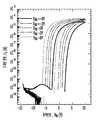
도 1은 종래기술에 따른 메모리 박막 트랜지스터의 드레인전류-게이트전압 특성을 나타내는 그래프
도 2a는 본 발명의 제1 실시예에 따른 이중 게이트 구조의 비휘발성 메모리 박막 트랜지스터의 단면도
도 2b는 본 발명의 제2 실시예에 따른 이중 게이트 구조의 비휘발성 메모리 박막 트랜지스터의 단면도
도 3a 내지 도 3g는 본 발명의 제1 실시예에 따른 이중 게이트 구조의 비휘발성 메모리 박막 트랜지스터의 제조방법을 설명하기 위한 공정 단면도
도 4a 내지 도 4d는 본 발명의 제2 실시예에 따른 이중 게이트 구조의 비휘발성 메모리 박막 트랜지스터의 제조방법을 설명하기 위한 공정 단면도
도 5는 본 발명의 일 실시예에 따라 제작된 이중 게이트 구조의 메모리 박막 트랜지스터의 드레인전류-게이트전압 특성을 트랜지스터의 문턱전압의 차이에 따라 나타낸 그래프
도 6a 및 도 6b는 본 발명의 제1 실시예에 따른 이중 게이트 구조의 메모리 박막 트랜지스터의 구동 방법을 설명하기 위한 회로도 및 타이밍도
도 7a 및 도 7b는 본 발명의 제2 실시예에 따른 이중 게이트 구조의 메모리 박막 트랜지스터의 구동 방법을 설명하기 위한 회로도 및 타이밍도
도 8a 및 도 8b는 본 발명의 일 실시예에 따라 제작된 이중 게이트 구조의 메모리 박막 트랜지스터의 게이트 전압- 드레인 전류 특성을 나타내는 그래프1 is a graph showing drain current-gate voltage characteristics of a memory thin film transistor according to the related art.
2A is a cross-sectional view of a non-volatile memory thin film transistor having a double gate structure according to a first embodiment of the present invention.
2B is a cross-sectional view of a non-volatile memory thin film transistor having a double gate structure according to a second embodiment of the present invention.
3A to 3G are cross-sectional views illustrating a method of manufacturing a non-volatile memory thin film transistor having a double gate structure according to a first embodiment of the present invention.
4A to 4D are cross-sectional views illustrating a method of manufacturing a non-volatile memory thin film transistor having a double gate structure according to a second embodiment of the present invention.
FIG. 5 is a graph illustrating drain current-gate voltage characteristics of a memory thin film transistor having a double gate structure according to an embodiment of the present invention according to a difference in threshold voltages of transistors.
6A and 6B are a circuit diagram and a timing diagram for explaining a method of driving a memory thin film transistor having a dual gate structure according to a first embodiment of the present invention.
7A and 7B are a circuit diagram and a timing diagram for describing a method of driving a memory thin film transistor having a double gate structure according to a second embodiment of the present invention.
8A and 8B are graphs showing gate voltage-drain current characteristics of a memory thin film transistor having a double gate structure according to an embodiment of the present invention.
이하 첨부된 도면을 참조하면서 본 발명의 바람직한 실시예를 상세히 설명한다. 다음에서 설명되는 실시예는 여러 가지 다른 형태로 변형될 수 있으며, 본 발명의 범위가 아래에서 상술되는 실시예에 한정되는 것은 아니다. 본 발명의 실시예들은 당해 분야에서 통상의 지식을 가진 자에게 본 발명을 보다 완전하게 설명하기 위하여 제공되는 것이다. 도면에 있어서, 층 영역들의 두께는 명확성을 기하기 위하여 실제 두께에 비해 과장되어 도시될 수 있다. 또한, 층이 다른 층 또는 기판 상에 있다고 언급된 경우에 그것은 다른 층 또는 기판 상에 직접 형성될 수 있거나 또는 그들 사이에 제3의 층이 게재될 수도 있다. 실시예 전체에 걸쳐서 동일한 참조부호는 동일한 구성요소를 나타낸다.
Hereinafter, exemplary embodiments of the present invention will be described in detail with reference to the accompanying drawings. The embodiments described below may be modified in various other forms, and the scope of the present invention is not limited to the embodiments described below. Embodiments of the present invention are provided to more fully explain the present invention to those skilled in the art. In the drawings, the thicknesses of layer regions may be exaggerated relative to actual thickness for clarity. Also, if it is mentioned that the layer is on another layer or substrate, it may be formed directly on the other layer or the substrate or a third layer may be interposed therebetween. Like reference numerals denote like elements throughout the embodiments.
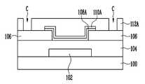
도 2a는 본 발명의 제1 실시예에 따른 이중 게이트 구조의 비휘발성 메모리 박막 트랜지스터의 단면도로서, 소오스 및 드레인 전극이 형성된 후에 채널막이 형성된 경우를 나타낸다.FIG. 2A is a cross-sectional view of a non-volatile memory thin film transistor having a double gate structure according to a first embodiment of the present invention, and illustrates a case where a channel film is formed after source and drain electrodes are formed.
도시된 바와 같이, 본 발명의 제1 실시예에 따른 이중 게이트 구조의 비휘발성 메모리 박막 트랜지스터는 기판(100) 상에 형성된 제1 게이트전극(102), 제1 게이트전극(102) 상에 형성된 제1 게이트절연막(104), 제1 게이트절연막(104) 상에 소정 간격으로 형성된 소오스 및 드레인 전극(106), 소오스 및 드레인 전극(106) 사이의 제1 게이트절연막(104) 상에 형성된 채널막(108A), 채널막(108A) 상에 형성된 제2 게이트절연막(112A) 및 제2 게이트절연막(112A) 상에 형성된 제2 게이트전극(118)을 포함한다. 또한, 채널막(108A)상에 형성된 보호막(110A) 및 제2 게이트절연막(112A)을 관통하는 콘택플러그(114)에 의해 소오스 및 드레인 전극(106)과 연결된 소오스 및 드레인 전극 패드(116)를 더 포함하는 것이 바람직하다.As illustrated, the non-volatile memory thin film transistor having a double gate structure according to the first embodiment of the present invention includes a
기판(100)은 유연하고 투명하거나, 경우에 따라서는 두 가지 특징 중 한 가지 특징을 갖는 물질로 형성되는 것이 바람직하며, 예를 들어 유리 기판 또는 플라스틱 기판일 수 있다.The
제1 게이트전극(102)은 투명한 전도성 박막으로 형성되는 것이 바람직하며, 예를 들어, 전도성 산화물 물질인 ITO(인듐-주석 산화물) 또는 ITO와 비슷한 정도의 충분히 높은 전도성과 충분한 투명도 특성을 갖는 전도성 산화물 박막으로 형성될 수 있다. 경우에 따라서는, 본 발명에서 제안하는 메모리 박막 트랜지스터의 응용 시스템이 요구하는 특성에 따라, 통상적인 박막 트랜지스터의 제작에서 사용되는 금속 박막으로 제1 게이트전극(102)을 형성할 수도 있다.The
제1 게이트절연막(104)은 산화물 절연체 박막으로 형성되는 것이 바람직하다. 예를 들어, 실리콘 산화막(SiO2), 실리콘질화막(SiNx), 실리콘산질화막(SiON) 등의 실리콘 계열 절연막으로 형성되거나, 알루미늄 산화막(Al2O3), 하프늄 산화막(HfO2), 지르코늄 산화막(ZrO2), 티타늄 산화막(TiO2) 등으로 형성될 수 있으며, 두 가지 이상의 금속 원소가 혼합된 산화막으로 형성될 수 있다. 또는, 앞서 언급된 산화물을 구성하는 금속 원소와 실리콘이 혼합된 실리케이트 절연막으로 형성될 수 있다. 이외에도 통상적인 산화물 박막 트랜지스터의 제작에 있어서 게이트 절연막 재료로 사용 가능한 산화물 절연막 소자들을 이용하여 제1 게이트절연막(104)을 형성할 수 있다. 또한, 제1 게이트절연막(104)는 소재의 유연성을 확보하거나 향상시키기 위하여, 절연 특성이 우수한 유기물 절연체 박막을 이용하여 형성될 수도 있다.The first
소오스 및 드레인 전극(106)은 투명한 전도성 박막으로 형성되는 것이 바람직하다. 예를 들어, ITO 또는 ITO와 유사한 정도의 전도성 및 투명도 특성을 갖는 전도성 산화물 박막으로 형성될 수 있다. 경우에 따라서는, 본 발명에서 제안하는 메모리 박막 트랜지스터의 응용 시스템이 요구하는 특성에 따라, 통상적인 박막 트랜지스터의 제작에서 사용되는 금속 박막을 이용하여 소오스 및 드레인 전극(106)을 형성할 수 있다.The source and drain
여기서, 소오스 및 드레인 전극(106)은 제1 게이트절연막(104) 상에 전기적으로 분리된 두 개의 영역에 소정의 간격으로 형성되며, 소오스 전극과 드레인 전극 사이의 영역이 메모리 박막 트랜지스터의 채널 영역으로 정의된다. 따라서, 소오스 및 드레인 전극(106)의 패턴 폭 및 패턴 사이의 거리에 의해 메모리 박막 트랜지스터의 채널 폭 및 길이가 결정되며, 메모리 트랜지스터의 동작 특성을 고려하여 채널 폭 및 길이를 적절하게 설계하는 것이 바람직하다.Here, the source and drain
채널막(108A)은 소오스 및 드레인 전극(106)의 사이, 즉, 메모리 박막 트랜지스터의 채널 영역에 형성되는데, 소오스 및 드레인 전극(106)의 측벽 및 상부의 일부를 덮도록 형성될 수 있다.The
여기서, 채널막(108A)은 메모리 박막 트랜지스터의 반도체로서의 역할을 수행한다. 채널막(108A)은 산화물반도체로 형성되는 것이 바람직하며, 특히, 에너지 밴드갭이 넓어 가시광 영역에서 투명한 성질을 갖는 산화물이면서 전기적으로 반도체의 성질을 갖는 투명한 산화물반도체 박막으로 형성되는 것이 더욱 바람직하다. 예를 들어, 아연 산화물(ZnO), 인듐-갈륨-아연 산화물(In-Ga-Zn-O), 아연-주석 산화물(Zn-Sn-O)로 형성되거나, 아연, 인듐, 갈륨, 주석, 알루미늄 중 적어도 두 개 이상의 원소를 포함하는 산화물로 형성될 수 있다. 또는, 앞서 언급한 산화물에 다양한 원소를 도핑하여 형성할 수 있다.Here, the
보호막(110A)은 후속 공정시 채널막(108A)의 손상을 방지하고, 메모리 박막 트랜지스터의 특성을 향상시키기 위한 것이다. 여기서, 보호막(110A)은 채널막(108A)의 상부에 형성되는데, 채널막(108A)과 함께 소오스 및 드레인 전극(106) 사이의 채널 영역에 형성되며, 소오스 및 드레인 전극층(106)의 측벽 및 상부의 일부를 덮도록 형성될 수 있다.The
여기서, 보호막(110A)의 역할을 자세하게 살펴보면 다음과 같다.Here, the role of the
첫 번째, 보호막(110A)은 채널막(108A)의 식각 공정 및 식각 마스크 제거 공정시 채널막(108A)의 공정 열화 현상을 억제한다. 보호막(110A)없이 식각 공정 및 식각 마스크 제거 공정을 수행하는 경우, 포토레지스트, 포토레지스트 현상액, 포토레지스트 박리액 등의 화학 약품이 채널막(108A)에 직접 작용하여 채널막(108A)의 재료적 특성을 열화시킬 수 있다. 따라서, 채널막(108A) 상에 보호막(110A)을 형성함으로써 채널막(108)이 화학적으로 열화되는 것을 방지할 수 있다.First, the
두 번째, 보호막(110A)은 제2 게이트절연막(112A) 형성 과정에서 채널막(108A)이 손상 및 열화되는 것을 방지함으로써, 채널막(108A)이 반도체로서의 역할을 충실히 수행하여 메모리 트랜지스터가 양호한 동작 특성을 갖게 한다.Second, the
예를 들어, 제2 게이트절연막(112A)이 유기 강유전체로 형성되는 경우, 유기 강유전체막은 유기 용액을 이용하는 도포 공정에 의해 형성되는데, 이때 사용되는 유기 용액의 종류에 따라 채널막(108A)의 재료적인 특성이 열화될 수 있다. 따라서, 채널막(108A) 상에 보호막(110A)을 형성함으로써 채널막(108A)이 화학적으로 열화되는 것을 방지할 수 있다.For example, when the second
세 번째, 보호막(110A)의 물질 종류 및 형성시의 공정 조건을 변화시켜 채널막(108A)의 전기적인 특성을 변화시킬 수 있다. 예를 들어, 보호막(110A) 형성시의 공정 조건을 변경하여 채널막(108A)의 캐리어 농도, 표면의 화학적 상태 등을 변화시킴으로써, 메모리 박막 트랜지스터의 동작 특성을 개선할 수 있다.Third, the electrical characteristics of the
네 번째, 보호막(110A)을 이용하여 제2 게이트절연막(112A)의 누설 전류를 억제할 수 있다. 예를 들어, 제2 게이트절연막(112A)이 유기 강유전체로 형성되는 경우, 유기 강유전체막은 그 소재의 특성상 박막화를 진행할수록 누설전류가 크게 증가하게 되며, 그에 따라, 메모리 박막 트랜지스터의 동작특성이 저하된다. 따라서, 유기 강유전체로 형성된 제2 게이트절연막(112A)과 채널막(108A) 사이에 보호막(110A)을 개재시킴으로써, 누설전류에 따른 메모리 박막 트랜지스터의 특성 저하를 방지할 수 있다.Fourth, the leakage current of the second
전술한 바와 같은 보호막(110A)의 역할을 고려할 때, 보호막(110A)은 첫째, 채널막(108A)의 공정 열화 현상을 충분히 억제할 수 있고, 둘째, 메모리 트랜지스터의 동작 특성을 개선할 수 있으며, 셋째, 제2 게이트절연막(112A)의 누설전류를 충분히 억제할 수 있는 전기적 특성을 보유하고 있는 물질로 형성되는 것이 바람직하다.Considering the role of the
따라서, 보호막(110A)은 산화물 절연체 박막으로 형성되는 것이 바람직하며, 예를 들어, 실리콘 산화막(SiO2), 실리콘질화막(SiNx), 실리콘산질화막(SiON) 등의 실리콘 계열 절연막으로 형성되거나, 알루미늄 산화막(Al2O3), 하프늄 산화막(HfO2), 지르코늄 산화막(ZrO2), 티타늄 산화막(TiO2) 등으로 형성될 수 있으며, 두 가지 이상의 금속 원소가 혼합된 산화막으로 형성될 수 있다. 또는, 앞서 언급된 산화물을 구성하는 금속 원소와 실리콘이 혼합된 실리케이트 절연막으로 형성될 수 있다. 물론, 이외에도 통상적인 산화물 박막 트랜지스터의 제작에 있어서 게이트 절연막 재료로 사용 가능한 산화물 절연막 물질들로 형성될 수 있다.Therefore, the
제2 게이트절연막(112A)은 메모리 박막 트랜지스터의 메모리 동작을 구현하기 위한 메인 게이트절연막으로서 사용되며, 유기 소재 즉 저분자 또는 고분자의 유기물 재료로 전압의 인가에 따라 잔류분극 현상을 보이는 유기 강유전체로 형성되는 것이 바람직하다.The second
예를 들어, 제2 게이트절연막(112A)은 P(VDF)(poly(vinylidene fluoride) 및 P(VDF)에 적절한 비율의 TrFE(Trifluorotethylene)가 혼합된 공중합체인 P(VDF-TrFE)로 형성될 수 있다. P(VDF)와 TrFE의 혼합 조성 범위는 P(VDF-TrFE)가 강유전 특성을 나타내는 범위 내에서 조절될 수 있으며, 예를 들어, P(VDF)가 55% 이상 포함되는 것이 바람직하다. 물론, 혼합 조성 범위는 제2 게이트절연막(112A)의 누설 전류 특성 및 강유전성을 최적화하기 위해 적절한 비율로 조절되는 것이 더욱 바람직하다.For example, the second
소오스 및 드레인 전극 패드(116)는 제2 게이트절연막(112A)을 관통하여 형성된 콘택플러그(114)를 통해 소오스 및 드레인 전극층(106)과 전기적으로 연결된다. 여기서, 소오스 및 드레인 전극 패드(116)은 투명한 전도성 박막으로 형성되는 것이 바람직하며, 예를 들어 ITO 또는 ITO와 유사한 정도의 전도성 및 투명도 특성을 갖는 전도성 산화물 박막으로 형성될 수 있다. 경우에 따라서는, 본 발명에서 제안하는 메모리 박막 트랜지스터의 응용 시스템이 요구하는 특성에 따라, 통상적인 박막 트랜지스터의 제작에서 사용되는 금속 박막을 이용하여 소오스 및 드레인 전극 패드(116)를 형성할 수 있다.The source and drain
제2 게이트전극(118)은 제2 게이트절연막(112)의 상부 일부에 위치하는데, 특히, 메모리 박막 트랜지스터의 채널 영역 상부에 위치한다. 여기서, 제2 게이트전극(118)은 투명한 전도성 박막으로 형성되는 것이 바람직하며, 예를 들어 ITO 또는 ITO와 유사한 정도의 전도성 및 투명도 특성을 갖는 전도성 산화물 박막으로 형성될 수 있다. 경우에 따라서는, 본 발명에서 제안하는 메모리 박막 트랜지스터의 응용 시스템이 요구하는 특성에 따라, 통상적인 박막 트랜지스터의 제작에서 사용되는 금속 박막으로 형성될 수도 있다.
The
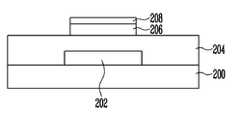
도 2b는 본 발명의 제2 실시예에 따른 이중 게이트 구조의 비휘발성 메모리 박막 트랜지스터의 단면도로서, 채널막이 형성된 후에 소오스 및 드레인 전극이 형성된 경우를 나타낸다. 단, 제1 실시예에서 설명된 내용과 중복되는 사항은 생략하여 설명하도록 한다.FIG. 2B is a cross-sectional view of a non-volatile memory thin film transistor having a double gate structure according to a second embodiment of the present invention, and illustrates a case where source and drain electrodes are formed after a channel film is formed. However, details overlapping with those described in the first embodiment will be omitted.
도시된 바와 같이, 상기 메모리 박막 트랜지스터는 기판(200) 상에 형성된 제1 게이트전극(202), 제1 게이트절연막(204), 채널막(206), 보호막(208), 소오스 및 드레인 전극(210), 제2 게이트절연막(212), 제2 게이트절연막(212)을 관통하는 콘택플러그(214)에 의해 소오스 및 드레인 전극(210)과 각각 연결된 소오스 및 드레인 전극 패드(216) 및 제2 게이트전극(218)을 포함한다.As illustrated, the memory thin film transistor may include a
제2 실시예에 따르면, 채널막(206) 및 보호막(208)이 형성된 후에 소오스 및 드레인 전극(210)이 형성되며, 채널막(206) 및 보호막(208)의 측벽 및 상부 일부를 덮도록 소오스 및 드레인 전극(210)이 형성된다.According to the second embodiment, the source and drain
이와 같은 제2 실시예의 구조에 따르면, 현행 공정에서 버텀게이트형 박막 트랜지스터를 제조하기 위해 업계에서 통상적으로 실시하고 있는 소자 구조를 소오스 및 드레인 전극(210)층까지 동일하게 적용할 수 있으므로, 업계 설비투자 비용을 최소화하고 신규 공정개발의 부담을 줄일 수 있다.According to the structure of the second embodiment, since the device structure conventionally implemented in the industry to manufacture the bottom gate type thin film transistor in the current process can be equally applied to the source and
한편, 채널막(206)을 형성한 후에 소오스 및 드레인 전극(206)을 형성하는 경우, 후속 공정을 수행하는 과정에서 채널막(206)이 열화될 가능성이 있다. 그러나, 본 발명에 따르면 채널막(206) 상에 보호막(208)을 형성함으로써 후속 공정에서의 채널막(206)의 열화를 방지할 수 있다. 즉, 제2 실시예에 의해 채널막(206) 상에 형성되는 보호막(208)은 앞서 제1 실시예에서 설명한 보호막(208)에 비해 다음의 역할을 더 수행하게 된다.On the other hand, in the case where the source and drain
첫 번째, 보호막(208)은 습식 또는 건식 식각에 의한 소오스 및 드레인 전극(210) 패터닝 공정 수행시, 채널막(206)의 공정 열화 현상을 차단하여 채널막(206)의 소재 특성이 열화되는 것을 방지할 수 있다.First, the
두 번째, 보호막(208)은 소오스 및 드레인 전극(210)을 패터닝하기 위한 식각 공정에서 식각 정지막으로서의 역할을 수행할 수 있다.Second, the
이와 같은 보호막(208)의 역할을 고려할 때, 보호막(208)은 채널막(206)의 공정 열화 현상을 충분히 억제할 수 있는 물질로 형성되는 것이 바람직하다. 또한, 식각 정지막으로서의 역할을 충분히 수행할 수 있도록, 상하 구성층 간에 충분한 식각 선택비를 갖는 물질로 이루어지는 것이 바람직하다. 즉, 소오스 및 드레인 전극(210)의 물질과 식각 선택비가 큰 물질로 이루어지는 것이 바람직하다.In consideration of the role of the
따라서, 보호막(208)은 산화물 절연체 박막으로 형성되는 것이 바람직하다. 예를 들어, 실리콘 산화막(SiO2), 실리콘질화막(SiNx), 실리콘산질화막(SiON) 등의 실리콘 계열 절연막으로 형성되거나, 알루미늄 산화막(Al2O3), 하프늄 산화막(HfO2), 지르코늄 산화막(ZrO2), 티타늄 산화막(TiO2) 등으로 형성될 수 있으며, 두 가지 이상의 금속 원소가 혼합된 산화막으로 형성될 수 있다. 또는, 앞서 언급된 산화물을 구성하는 금속 원소와 실리콘이 혼합된 실리케이트 절연막으로 형성될 수 있다. 물론, 이외에도 통상적인 산화물 박막 트랜지스터의 제작에 있어서 게이트 절연막 재료로 사용 가능한 산화물 절연막 물질들을 이용하여 보호막(208)을 형성할 수 있으며, 앞서 제1 실시예에 설명한 보호막(110A)으로 사용 가능한 물질을 동시에 사용하는 것 또한 가능하다.Therefore, the
전술한 바와 같이 본 발명의 제1, 제2 실시예에 따르면, 유연성, 투명성, 또는 두 가지 특성을 동시에 확보하면서 메모리 소자의 기능을 갖는 이중 게이트 구조의 비휘발성 메모리 박막 트랜지스터를 제공할 수 있다.As described above, according to the first and second embodiments of the present invention, a double gate nonvolatile memory thin film transistor having a function of a memory device while simultaneously securing flexibility, transparency, or two characteristics can be provided.
이하, 도면을 참조하여 본 발명의 제1, 제2 실시예에 따른 이중 게이트 구조의 비휘발성 메모리 박막 트랜지스터의 제조방법을 살펴보도록 한다.
Hereinafter, a method of manufacturing a nonvolatile memory thin film transistor having a double gate structure according to the first and second embodiments of the present invention will be described with reference to the accompanying drawings.
도 3a 내지 도 3g는 본 발명의 제1 실시예에 따른 이중 게이트 구조의 비휘발성 메모리 박막 트랜지스터의 제조방법을 설명하기 위한 공정 단면도로서, 앞서 도 2a를 참조하여 설명된 구조의 메모리 박막 트랜지스터를 제조하는 방법에 대해 설명하도록 한다.3A to 3G are cross-sectional views illustrating a method of manufacturing a non-volatile memory thin film transistor having a double gate structure according to a first embodiment of the present invention, and manufacturing a memory thin film transistor having the structure described with reference to FIG. 2A. Explain how to do this.
도 3a에 도시된 바와 같이, 기판(100)을 제공한다. 여기서, 기판(100)은 유리 또는 플라스틱 기판일 수 있다. 플라스틱 기판일 경우, 기판(100) 자체의 평활도 개선을 위해 적절한 전처리 과정을 수행한 후에 제공될 수 있다. 또한, 플라스틱 기판일 경우, 기판(100) 자체의 내열 특성을 개선하기 위해 적절한 기판 제조 공정을 수행한 후에 제공될 수 있다.As shown in FIG. 3A, a
이어서, 기판(100) 상에 제1 게이트전극용 도전막을 형성한 후, 이를 패터닝 하여 제 1게이트전극(102)을 형성한다. 여기서, 제1 게이트전극용 도전막은 스퍼터링 방식에 의해 형성될 수 있으며, 패터닝 공정은 습식 또는 건식 식각 공정에 의해 수행될 수 있다. 또한, 제1 게이트전극(102)는 100 내지 200nm의 두께로 형성되는 것이 바람직하다.Subsequently, the first gate electrode conductive film is formed on the
이어서, 제1 게이트전극(102)이 형성된 결과물의 전체 구조상에 제1 게이트절연막(104)를 형성한다. 여기서, 제1 게이트절연막(104)는 통상의 반도체 제조 공정에서 사용되는 박막 형성 공정 방법에 의해 형성될 수 있는데, 예를 들어, 스퍼터링법, 화학적 기상증착법(CVD), 원자층 증착법(ALD) 등을 이용하여 형성될 수 있다. 한편, 제1 게이트절연막(104)의 두께는 이중 게이트 구조를 갖는 메모리 박막 트랜지스터에 요구되는 특성을 고려하여 적절하게 선택하는 것이 바람직하다. 즉, 박막 트랜지스터의 동작을 위한 문턱전압의 값 및 조절전압인가 조건하에서의 드레인 전류값을 만족할 수 있도록 제1 게이트절연막(104)의 두께를 선택하는 것이 바람직하다.Subsequently, a first
이어서, 제1 게이트절연막(104) 상에 소오스 및 드레인 전극용 도전막을 형성한 후, 이를 패터닝하여 소오스 및 드레인 전극(106)을 형성한다. 여기서, 소오스 및 드레인 전극용 도전막은 스퍼터링 방식에 의해 형성될 수 있으며, 패터닝 공정은 습식 또는 건식 식각 공정에 의해 수행될 수 있다. 또한, 소오스 및 드레인 전극(106)은 100 내지 200nm의 두께로 형성되는 것이 바람직하다.Subsequently, a source and drain electrode conductive film is formed on the first
도 3b에 도시된 바와 같이, 소오스 및 드레인 전극(106)가 형성된 결과물의 전면을 따라 채널용 물질막(108)을 형성한다. 본 실시예에서는 가시광 영역에서 투명한 산화물 반도체로 채널용 물질막(108)을 형성하는 경우에 대해 설명하도록 한다.As shown in FIG. 3B, the
여기서, 채널용 물질막(108)의 두께는 메모리 박막 트랜지스터의 동작조건을 결정하는 중요한 소자 변수의 하나이므로, 다음의 사항을 고려하여 채널용 물질막(108)의 두께를 결정하는 것이 바람직하다.Here, since the thickness of the
첫째, 메모리 박막 트랜지스터의 동작 특성을 확보할 수 범위 내에서 채널용 물질막(108)의 두께를 결정한다. 일반적으로 박막 트랜지스터의 채널 영역의 반도체 박막으로서 기능하기 위해서는 5 내지 50nm의 두께로 채널용 물질막(108)을 형성하는 것이 바람직하다.First, the thickness of the
만약, 5nm 보다 막 두께가 얇은 경우에는 채널막의 표면을 이동하는 캐리어의 평균 이동거리보다 막 두께가 얇아지게 되어 캐리어의 이동도를 크게 떨어뜨리는 원인이 될 수 있다. 한편, 50nm 보다 막 두께가 두꺼운 경우에는 채널막의 내부의 캐리어 농도가 과도해져 박막 트랜지스터의 전기적인 동작 특성에 있어서 오프 전류의 증가와 트랜지스터의 온/오프 동작 마진의 감소를 초래할 수 있으며, 극단적으로 캐리어 농도가 높은 경우에는 구동 트랜지스터의 동작 자체를 확보할 수 없게 된다. 따라서 첫 번째 사항을 고려할 때 채널용 물질막(108)의 두께는 5 내지 50nm 인 것이 바람직하다.If the film thickness is thinner than 5 nm, the film thickness becomes thinner than the average moving distance of the carrier moving on the surface of the channel film, which may cause the carrier mobility to be greatly reduced. On the other hand, if the film thickness is greater than 50 nm, the carrier concentration inside the channel film becomes excessive, which may result in an increase in the off current and a decrease in the on / off operation margin of the transistor in the electrical operating characteristics of the thin film transistor, and extremely If the concentration is high, the operation of the driving transistor itself cannot be ensured. Therefore, in consideration of the first matter, the thickness of the
둘째, 메모리 박막 트랜지스터의 메모리 동작을 보다 낮은 전압에서 수행할 수 있도록 채널용 물질막(108)의 두께를 결정한다. 본 명세서에서는 메모리 트랜지스터의 동작전압을 결정하기 위한 정량적인 계산에 대해서는 설명을 생략하나, 메모리 트랜지스터의 동작전압은 온 쓰기 동작(예를 들어, 데이터 "1" 저장)보다 오프 쓰기 동작(예를 들어, 데이터 "0" 저장)에 더 높은 동작전압을 요구한다. 그 이유는 산화물반도체로 형성된 채널막의 경우, 그 소재의 특성상, 인가 전압의 변화에 따라 반전층과 축적층에서 동작하는 통상적인 실리콘 반도체와는 달리, 인가 전압의 변화에 따라 공핍층과 축적층에서 동작하며, 특정 전압 조건에서 산화물반도체 박막은 완전 공핍화되어 절연체와 같이 거동하는 특징을 갖기 때문이다. 이와 같은 조건 하에서는 메모리 트랜지스터를 구성하는 게이트 스택 구조 상에서 산화물반도체 박막의 완전 공핍층의 존재로 인해 형성된 직렬 커패시터에 의해 쓰기 전압의 손실이 발생하게 되며 결과적으로 오프 쓰기 동작시 동작전압의 상승을 초래하는 원인이 된다. 따라서, 이러한 효과를 가능한 수준에서 억제하고 오프 쓰기 동작시 쓰기 전압을 줄이기 위해서는 채널막의 완전 공핍층의 두께를 가능한 한 줄일 필요가 있으며, 이는 채널용 물질막(108)의 두께를 가능한 한 줄일 필요가 있음을 의미한다. 따라서, 두 번째 사항을 고려할 때 채널용 물질막(108)의 증착 두께는 20nm 이하인 것이 바람직하다.Second, the thickness of the
결과적으로, 상기 첫 번째 사항과 두 번째 사항을 동시에 고려하여 채널용 물질막(108)의 두께는 5 내지 20nm의 범위에서 결정되는 것이 더욱 바람직하다.As a result, it is more preferable that the thickness of the
또한, 채널용 물질막(108)은 스퍼터링(sputtering) 방법, 화학적기상증착법(chemical vapor deposition), 원자층 증착법(atomic layer deposition), 펄스레이저 증착법(pulsed-laser deposition), 솔젤용액을 이용하는 스핀코팅(spin-coating) 방법, 전구체 잉크를 이용하는 인쇄방법 등 산화물 박막을 형성하기 위해 통상적으로 사용되는 모든 증착방법을 사용하여 형성될 수 있으며, 이들 방법을 병용 또는 변용하여 사용하는 것도 가능하다.In addition, the
도 3c에 도시된 바와 같이, 채널용 물질막(108) 상에 보호막용 물질막(110)을 형성한다. 여기서, 보호용 물질막(110)의 두께는 메모리 박막 트랜지터의 동작 특성을 결정하는 매우 중요한 소자 변수의 하나로서, 다음의 사항을 고려하여 두께를 결정하는 것이 바람직하다.As shown in FIG. 3C, the
첫째, 메모리 트랜지스터의 동작전압이 너무 증가하지 않는 범위에서 보호용 물질막(110)의 두께를 결정하여야 한다. 보호용 물질막(110)의 두께가 너무 두꺼운 경우, 메모리 트랜지스터의 구동 전압의 일부가 트랜지스터의 게이트 스택의 일부를 구성하는 보호막에 의해 생기는 직렬 커패시터에서 소모되어 전체적으로 동작전압을 상승시키는 원인이 될 수 있기 때문이다. 따라서, 첫 번째 사항을 고려할 때 보호용 물질막(110)의 두께는 10nm 이하의 범위에서 결정되는 것이 바람직하다.First, the thickness of the
둘째, 채널용 물질막(108)의 식각 공정시, 각종 화학약품으로부터 초래되는 공정 열화를 충분히 억제할 수 있는 범위에서 보호용 물질막(110)의 두께를 결정하여야 한다.Second, during the etching process of the
셋째, 후속 공정에서 형성될 제2 게이트절연막의 누설 전류를 충분히 억제할 수 있는 범위에서 보호용 물질막(110)의 두께를 결정하여야 한다.Third, the thickness of the
따라서, 두 번째 및 세 번째 사항을 고려할 때 보호용 물질막(110)의 두께는 4nm 이상인 것이 바람직하며, 결과적으로, 첫 번째 내지 세 번째 사항을 동시에 고려할 때, 보호용 물질막(110)의 두께는 4 내지 10nm의 범위에서 결정되는 것이 바람직하다.Therefore, the thickness of the
또한, 보호용 물질막(110)은 스퍼터링(sputtering) 방법, 화학적기상증착법(chemical vapor deposition), 원자층 증착법(atomic layer deposition), 펄스레이저 증착법(pulsed-laser deposition), 솔젤용액을 이용하는 스핀코팅(spin-coating) 방법, 전구체 잉크를 이용하는 인쇄방법 등 산화물 박막을 형성하기 위해 통상적으로 사용되는 모든 증착방법을 사용하여 형성될 수 있으며, 이들 방법을 병용 또는 변용하여 사용하는 것도 가능하다. 특히, 보호용 물질막(110)의 형성 방법은 하부에 형성된 채널용 물질막(108)의 특성을 열화시키기 않도록 공정온도, 플라즈마의 사용여부, 박막형성 원료 등을 결정하는 것이 바람직하다. 또한, 양질의 계면 형성을 위해 채널용 물질막(108)과 보호용 물질막(110)의 형성 공정은 동일한 장비 내에서 연속적으로 수행하는 것이 더욱 바람직하다.In addition, the
도 3d에 도시된 바와 같이, 보호용 물질막(110) 및 채널용 물질막(108)을 식각하여 메모리 박막 트랜지스터의 채널 영역 상에 채널막(108A) 및 보호막(110A)을 형성한다.As shown in FIG. 3D, the
여기서, 보호용 물질막(110) 및 채널용 물질막(108)의 식각 공정은 통상적인 포토리소그래피 공정에 의해 수행될 수 있다. 예를 들어, 소정의 습식 식각용액을 사용하여 습식 식각공정을 수행하거나, 플라즈마를 이용하여 건식 식각공정을 수행할 수 있다. 식각 공정을 수행하는 과정에서, 보호막(110A)은 채널막(108A)이 열화되는 것을 효과적으로 방지한다.Here, the etching process of the
도 3e에 도시된 바와 같이, 채널막(108A) 및 보호막(110A)이 형성된 결과물의 전체 구조 상에 제2 게이트절연막(112)을 형성한다. 본 실시예에서는 유기 강유전체를 이용하여 제2 게이트절연막(112)을 형성하는 경우에 대해 설명하도록 한다.As shown in FIG. 3E, the second
여기서, 제2 게이트절연막(112)은 스핀 코팅 방식에 의해 형성되는 것이 바람직하다. 예를 들어, P(VDF-TrFE)를 선택하여 제2 게이트절연막(112)을 형성하는 경우, 통상적으로 고체 알갱이 형태의 P(VDF-TrFE) 원료를 적절한 유기 용매에 용해시키는 방법으로 원료 용액을 제조할 수 있다. 스핀 코팅 방법에 의해 제2 게이트절연막(112)을 형성하는 통상적인 순서는 다음과 같다. 먼저, 원료 용액을 소정의 기판 위에 적하하여 적절한 스핀 코팅 조건으로 코팅한 후, 원료 용액에 포함된 유기 용매를 휘발시키기 위해 소정의 온도에서 열처리를 수행한다. 이어서, 유기 강유전체막의 결정화 과정을 위해 소정의 온도에서 열처리를 수행한다. 통상적으로 유기 용매 휘발을 위한 열처리 공정의 온도는 사용하는 유기 용매에 따라 다를 수는 있으나, 50 내지 120oC에서 수행되는 것이 바람직하다. 또한, 결정화를 위한 열처리 공정의 온도는 사용하는 유기 강유전체의 물질 종류에 따라 다를 수 있으나, 유기 강유전체 소재로서 P(VDF-TrFE)를 사용하는 경우, 120 내지 160oC 사이의 온도에서 수행되는 것이 바람직하다. 이때, 제2 게이트절연막(112)이 양호한 강유전 특성을 갖도록 하기 위해서는 박막의 결정화 과정이 필수적이기 때문에 결정화 온도를 선택하는 것은 매우 중요하다. 만일 결정화 공정의 온도가 너무 낮으면 박막의 결정화도가 부족하여 소망하는 전기적 특성을 얻기 어려우며, 반대로 결정화 공정의 온도가 너무 높으면 형성된 박막이 완전히 용융되어 강유전 특성을 소실할 우려가 있다.Here, the second
한편, 스핀 코팅 방식에 의해 제2 게이트절연막(112)을 형성하는 경우, 스핀 코팅 공정의 회전수 및 유기 강유전체 원료 용액의 농도 조절을 통해 제2 게이트절연막(112)의 두께를 조절할 수 있다. 여기서, 제2 게이트절연막(112)의 적절한 두께를 선택하기 위해서는 다음의 두 가지 사항을 고려해야 한다.On the other hand, when the second
첫째, 메모리 트랜지스터의 동작전압을 가능한 한 낮출 수 있는 방향으로 제2 게이트절연막(112)의 두께를 선택하는 것이 바람직하다. 이를 위해서는 상대적으로 낮은 인가 전압에서도 용이하게 분극의 반전이 가능하도록 가능한 한 제2 게이트절연막(112)의 두께를 줄이는 것이 바람직하다. 그러나, 기존의 연구 결과에 의하면, 유기 강유전체 박막의 두께가 일정 두께 이하로 얇아질 경우 박막 자체의 강유전성이 크게 열화하여, 분극 반전이 일어나는 전계값이 크게 증가하고, 동일 전계에서도 분극 반전에 필요한 시간이 매우 길어지는 현상이 나타난다는 사실이 알려져 있다. 이러한 열화 현상이 일어나는 임계 막 두께의 값은 유기 강유전체의 상하부에 어떤 전극을 사용하는가에 따라서도 달라질 수는 있으나 일반적으로 50nm 이하의 막 두께에서 현저하게 관찰되는 것으로 알려져 있다.First, it is preferable to select the thickness of the second
둘째, 메모리 트랜지스터 즉, 메모리 트랜지스터의 데이터 리텐션 특성을 향상시킬 수 있는 방향으로 제2 게이트절연막(112)의 두께를 선택하는 것이 바람직하다. 메모리 트랜지스터의 데이터 리텐션 시간은 제2 게이트절연막(112)의 누설 전류 특성과 매우 밀접한 관련이 있는 만큼 소자의 동작 중에 있어서 과도한 누설 전류가 발생하지 않도록 제2 게이트절연막(112)의 증착 두께를 최적화 할 필요가 있다. 연구 결과에 따르면, 유기 강유전체막의 막 두께가 200nm 정도에서는 인가 전압에 따른 현저한 누설 전류가 발생하지 않는 것이 알려져 있다.Second, it is preferable to select the thickness of the second
결과적으로, 첫 번째 사항과 두 번째 사항을 고려하여, 제2 게이트절연막(112)의 증착 두께는 50 내지 200nm의 범위에서 선택하는 것이 바람직하다. 다만, 향후 기술 개발에 따라 유기 강유전체막이 더욱 박막화되더라도 우수한 강유전 특성을 얻을 수 있는 방법이 개발된다면, 제2 게이트절연막(112)의 증착 두께 하한은 더욱 감소될 수 있다.As a result, in consideration of the first point and the second point, the deposition thickness of the second
도 3f에 도시된 바와 같이, 제2 게이트절연막(112)을 일부 식각하여, 소오스 및 드레인 전극(106)의 표면을 일부 노출시키는 콘택홀(C)을 형성한다. 본 도면에서는 콘택홀(C) 형성 과정에서 식각된 제2 게이트절연막을 도면 부호 "112A"로 도시하였다.As shown in FIG. 3F, the second
예를 들어, 제2 게이트절연막(112)의 상부에 프토레지스트 패턴을 형성한 후, 포토레지스트 패턴을 식각 마스크로 유기 강유전체 제2 게이트절연막(112)을 식각하고, 이어서, 식각 마스크인 포토레지스트 패턴을 제거함으로써 콘택홀(C)을 형성할 수 있다. 여기서, 콘택홀(C) 형성 공정은 다음의 두 가지 사항을 고려해야 한다.For example, after forming a photoresist pattern on the second
첫째, 산소 플라즈마를 이용하여 제2 게이트절연막(112)을 식각하는 경우, 채널막(108A)의 특성이 열화되지 않도록 산소 플라즈마의 조건을 최적화하여야 한다. 일반적으로 산화물 반도체로 형성된 채널막(108A)은 플라즈마 처리에 의해 표면 및 박막 내부의 특성이 상당히 변경될 가능성을 가지고 있다. 물론, 제2 게이트절연막(112)의 식각 공정시 보호막(110A)이 채널막(108A)의 보호막으로서 역할을 수행하기는 하지만, 채널막(108A)의 특성이 열화되지 않도록 산소 플라즈마 조건을 최적화할 필요가 있다.First, when etching the second
둘째, 식각 마스크로 이용한 포토 레지스트 패턴의 박리 공정시 제2 게이트절연막(112A)의 특성에 영향을 미치지 않는 박리액을 선택해야 한다. 일반적으로 사용되는 포토 레지스트 패턴의 박리를 위한 화학 약품들은 자칫 제2 게이트절연막(112A)의 특성에 치명적인 영향을 미칠 수 있기 때문에, 박리액의 선택에 충분한 주의를 기울여야 한다. 더구나, 포토레지스트 패턴의 제거 공정에서는 일반 습식 식각과는 달리 진공 중에서 플라즈마를 사용하는 일종의 건식 식각 공정을 채용하고 있기 때문에, 포토 레지스트 패턴의 경화 정도가 더욱 심하여 적절하지 않은 조건의 박리 과정에서는 포토 레지스트 패턴이 제2 게이트절연막(112A) 상부에 일부 잔류할 수도 있다.Second, in the peeling process of the photoresist pattern used as the etching mask, a peeling liquid that does not affect the characteristics of the second
이 공정에서 적용 가능한 박리액이 가져야 할 특성은 다음과 같다.The characteristics which the peeling solution applicable in this process should have are as follows.
첫 번째 특성은, 박리액의 구성 성분이 제2 게이트절연막(112A)에 화학적인 영향을 주지 않아야 한다. 예를 들어, P(VDF-TrFE)로 형성된 유기 강유전체 박막의 경우, 박리액의 구성 성분이 P(VDF-TrFE)를 화학적으로 해체하여 박막의 제거를 야기해서는 안되며, P(VDF-TrFE)이 제거되지는 않는다고 하더라도, P(VDF-TrFE)의 결정 상태 또는 화학적인 결합 상태를 크게 변화시켜, P(VDF-TrFE)의 전기적 특성에 심각한 변화를 초래해서는 안된다. 예를 들어, 포토 레지스트 패턴의 박리를 위해 일반적으로 적용되는 유기 약품의 하나인 아세톤(Acetone)의 경우, P(VDF-TrFE)를 완전히 용해시켜 제거하는 작용을 가지기 때문에, 본 발명에서 제공하는 제조 방법에서 아세톤을 박리액으로 사용하는 것은 불가능하다.The first characteristic is that the constituents of the stripping solution should not have a chemical influence on the second
두 번째 특성은, 해당 박리액이 포토 레지스트 패턴의 잔류 성분을 완전하게 제거할 수 있어야 한다. 만약, 해당 박리액이 포토 레지스트 패턴의 잔류 성분을 충분히 효과적으로 제거할 수 없는 경우, 포토 레지스트 패턴의 잔류 성분은 본 발명의 소자가 형성되어 있는 기판(100)의 일부에 계속 잔류하여, 본 발명의 소자가 정상적으로 동작하는 것을 방해하는 요인으로 작용할 가능성이 있다. 예를 들어, 포토 레지스트 패턴의 박리를 위해 메탄올을 주성분으로 하는 유기 약품을 사용할 수는 있으나, 사용한 포토 레지스트 패턴의 종류 및 선행 공정의 효과에 따라서는 메탄올(methanol)을 이용하여 포토 레지스트의 잔류 성분을 완전히 제거할 수 없다.The second property is that the stripper must be able to completely remove the residual components of the photoresist pattern. If the stripper cannot remove the remaining components of the photoresist pattern sufficiently effectively, the remaining components of the photoresist pattern remain on a part of the
도 3g에 도시된 바와 같이, 콘택홀(C)이 형성된 결과물의 전체 구조상에 도전막을 형성한다. 이때, 콘택홀(C) 내에 도전막이 매립되어 소오스 및 드레인 전극(106)에 각각 연결되는 콘택플러그(114)이 형성된다.As shown in FIG. 3G, a conductive film is formed on the entire structure of the resultant in which the contact hole C is formed. In this case, a
이어서, 도전막을 식각하여 콘택플러그(114)를 통해 소오스 및 드레인 전극(106)과 각각 연결되는 소오스 및 드레인 전극 콘택 패드(116) 및 메모리 트랜지스터의 채널 영역 상에 위치되는 제2 게이트전극(118)을 형성한다.Subsequently, the conductive layer is etched to connect the source and drain
여기서, 상기 도전막은 스퍼터링 방법에 의해 증착될 수 있다. 또한, 도전막은 메모리 박막 트랜지스터의 응용 분야에 따라 투명하지 않으나 통상적으로 사용되는 금속 도전막 박막으로 이루어질 수 있으며, 통상적으로 사용되는 소정의 방법에 의해 증착될 수 있다. 또한, 증착된 도전막은 물질의 종류에 따라 적절한 식각 공정에 의해 패터닝 할 수 있다.Here, the conductive film may be deposited by a sputtering method. In addition, the conductive film may be formed of a metal conductive film thin film which is not transparent depending on the application field of the memory thin film transistor, and may be deposited by a predetermined method commonly used. In addition, the deposited conductive film may be patterned by an appropriate etching process according to the type of material.
이때, 콘택플러그(114), 소오스 및 드레인 전극 패드(116) 및 제2 게이트전극(118)의 형성 공정 및 패터닝 공정은 하부에 기 형성된 제2 게이트절연막(112A)에 손상을 주지 않는 조건에서 수행되어야 한다. 그 이유는 다음과 같다.In this case, the process of forming and patterning the
첫 번째 이유는 플라즈마를 사용하는 통상적인 도전막의 증착공정이 유기 강유전체로 형성된 제2 게이트절연막(112A)의 전기적, 기계적인 박막 특성을 크게 열화시킬 가능성이 높기 때문이다.The first reason is that the deposition process of the conventional conductive film using plasma has a high possibility of greatly deteriorating the electrical and mechanical thin film characteristics of the second
두 번째 이유는 제2 게이트전극(118) 등을 형성하는 과정에서 제2 게이트절연막(112A)이 열화될 수 있기 때문이다. 전도성 산화물 박막을 제2 게이트전극(118) 등의 물질로 사용하는 경우, 전극의 전도도 향상을 위해 증착공정 이후 소정의 온도에서 후속 열처리 공정을 수행하는 경우가 많다. 따라서, 후속 열처리 공정 수행시 제2 게이트절연막(112A) 물질의 녹는점 보다 낮은 온도로 열처리 공정을 수행하여야 한다.The second reason is that the second
세 번째 이유는 제2 게이트 전극(118) 등의 식각 공정시 패터닝 프로파일이 불량해질 수 있기 때문이다. 제2 게이트절연막(112A) 형성시 사용되는 P(VDF-TrFE)는 표면의 거칠기 정도가 매우 심하여 통상적으로 사용하는 도전성 산화물 박막 층과의 밀착성이 좋지 않으며, 그에 따라, 제2 게이트 전극(118) 등의 패터닝이 불량해질 수 있다.The third reason is that the patterning profile may be poor during the etching process of the
따라서, 제2 게이트절연막(112A)에 손상을 주지 않으면서, 소오스 및 드레인 전극 패드(116), 제2 게이트전극(118)의 형상을 용이하게 형성할 수 있도록 전극 물질의 종류, 증착 공정 방법, 후속 열처리 공정 온도, 식각 공정 조건 등을 최적화하는 것이 바람직하다.
Therefore, the type of electrode material, the deposition process method, and the like, so that the shape of the source and drain
도 4a 내지 도 4d는 본 발명의 제2 실시예에 따른 이중 게이트 구조의 비휘발성 메모리 박막 트랜지스터의 제조방법을 설명하기 위한 공정 단면도로서, 앞서 도 2b를 참조하여 설명된 구조의 메모리 박막 트랜지스터를 제조하는 방법에 대해 설명하도록 한다. 단, 앞서 제1실시예에서 설명한 내용과 중복되는 내용은 생략하여 설명하도록 한다.4A through 4D are cross-sectional views illustrating a method of manufacturing a non-volatile memory thin film transistor having a double gate structure according to a second embodiment of the present invention. The memory thin film transistor having the structure described with reference to FIG. 2B is manufactured. Explain how to do this. However, descriptions overlapping with those described in the first embodiment will be omitted.
도 4a에 도시된 바와 같이, 기판(200) 상에 제1 게이트전극용 도전막을 형성한 후, 이를 식각하여 제1 게이트전극(202)을 형성한다. 이어서, 제1 게이트전극(202)이 형성된 결과물의 전체 구조 상에 제1 게이트절연막(204)를 형성한다.As shown in FIG. 4A, after the conductive film for the first gate electrode is formed on the
여기까지의 공정은 앞서 설명한 제1 실시예와 동일하게 진행된다.The process so far proceeds in the same manner as in the first embodiment described above.
도 4b에 도시된 바와 같이, 제1 게이트절연막(204)이 형성된 결과물의 전면을 따라 채널용 물질막 및 보호용 물질막을 차례로 형성한 후, 이들을 식각하여 메모리 박막 트랜지스터의 채널 영역 상에 채널막(206) 및 보호막(208)을 형성한다.As shown in FIG. 4B, the channel material film and the protective material film are sequentially formed along the entire surface of the resultant product in which the first
도 4c에 도시된 바와 같이, 채널막(206) 및 보호막(208)이 형성된 결과물의 전체 구조 상에 소오스 및 드레인 전극용 도전막을 형성한 후, 이를 식각하여 소오스 및 드레인 전극(210)을 형성한다.As shown in FIG. 4C, after forming the conductive film for the source and drain electrodes on the entire structure of the resultant product in which the
도 4d에 도시된 바와 같이, 소오스 및 드레인 전극(210)이 형성된 결과물의 전체 구조 상에 제2 게이트절연막(212)을 형성한 후, 이를 일부 식각하여 소오스 및 드레인 전극(210)의 표면을 일부 노출시키는 콘택홀을 형성한다.As shown in FIG. 4D, after forming the second
이어서, 콘택홀이 형성된 결과물의 전체 구조상에 도전막을 형성한 후, 이를 식각하여, 콘택홀 내에 매립된 콘택플러그(214), 콘택플러그(214)에 의해 소오스 및 드레인 전극(210)과 각각 연결되는 소오스 및 드레인 전극 패드(216) 및 제2 게이트전극(218)을 형성한다.Subsequently, after the conductive film is formed on the entire structure of the resultant contact hole, the conductive film is etched and connected to the source and drain
본 명세서에 기술된 제1, 제2 실시예에 따른 이중 게이트 구조의 메모리 박막 트랜지스터의 제조방법은 그 일례로 제시된 것이며, 본 발명이 이에 한정된 것은 아니다. 이 밖에도 응용하고자 하는 전체 시스템의 구조 및 그 요구 공정에 따라 구체적인 공정 조건은 가장 적절한 형태로 선택될 수 있다.
The manufacturing method of the memory thin film transistor having the double gate structure according to the first and second embodiments described herein is presented as an example, and the present invention is not limited thereto. In addition, specific process conditions may be selected in the most appropriate form according to the structure of the entire system to be applied and the required processes thereof.
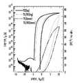
도 5는 본 발명의 일 실시예에 따라 제작된 이중 게이트 구조의 메모리 박막 트랜지스터의 드레인전류-게이트전압 특성을 나타낸 그래프이다.FIG. 5 is a graph illustrating drain current-gate voltage characteristics of a memory thin film transistor having a double gate structure according to an exemplary embodiment of the present invention.
전술한 바와 같은 본 발명에 따르면, 메모리 박막 트랜지스터에 이중 게이트 구조를 적용한다. 따라서, 메모리 박막 트랜지스터의 제1 게이트전극(102,202)에 조절전압을 인가함으로써 문턱전압을 용이하게 조절할 수 있다.According to the present invention as described above, the double gate structure is applied to the memory thin film transistor. Therefore, the threshold voltage can be easily adjusted by applying a control voltage to the
특히, 본 그래프에서는 메모리 박막 트랜지스터의 구동시 제1 게이트전극(102,202)에 음의 전압을 인가함으로써, 정전압 영역에서 문턱전압을 형성하는 경우를 나타낸다. 이때, 문턱전압을 설정함에 있어서 다음의 사항을 고려하는 것이 바람직하다.In particular, this graph illustrates a case where a threshold voltage is formed in the constant voltage region by applying a negative voltage to the
첫째, 메모리 박막 트랜지스터의 문턱전압을 설정함에 있어서, 게이트 전압이 0V인 경우, 메모리 박막 트랜지스터가 턴 오프된 상태에서 드레인 전류가 전혀 흐르지 않는 범위 내에서 메모리 박막 트랜지스터의 문턱전압을 설정하는 것이 바람직하다. 또한, 본 그래프에는 도시되지 않았으나, 메모리 박막 트랜지스터의 턴온 동작에서도 게이트전압 0V에서 드레인 전류가 흐르지 않을만큼 문턱전압을 정전압 영역에서 형성하는 것이 바람직하다. 이를 통해, 메모리 박막 트랜지스터의 문턱전압이 부전압 영역에서 형성됨에 따른 문제점 중 게이트 전압 0V에서 드레인 전류가 흐르는 것을 방지할 수 있다.First, in setting the threshold voltage of the memory thin film transistor, when the gate voltage is 0 V, it is preferable to set the threshold voltage of the memory thin film transistor within a range in which no drain current flows while the memory thin film transistor is turned off. . Although not shown in the graph, it is preferable to form the threshold voltage in the constant voltage region so that the drain current does not flow at the gate voltage of 0V even during the turn-on operation of the memory thin film transistor. As a result, it is possible to prevent the drain current from flowing at the gate voltage of 0V due to the threshold voltage of the memory thin film transistor being formed in the negative voltage region.
둘째, 메모리 박막 트랜지스터의 쓰기 동작시 온/오프 동작전압을 대칭적으로 인가할 수 있도록 문턱전압을 설정하는 것이 바람직하다. 즉, 쓰기 동작에 의해 실현되는 드레인 전류의 메모리 윈도우 폭이 게이트 전압 0V를 중심으로 형성되도록 한다. 이를 통해, 온 동작전압과 오프 동작전압의 비대칭으로 인해 회로가 복잡해지는 것을 방지할 수 있다.Second, it is preferable to set the threshold voltage so that the on / off operating voltage is symmetrically applied during the write operation of the memory thin film transistor. That is, the memory window width of the drain current realized by the write operation is formed around the
셋째, 게이트 전압 0V에서 리드 동작을 수행할 수 있도록 메모리 박막 트랜지스터의 문턱전압을 설정한다. 이를 통해, 가능한 한 작은 값의 전압수준을 유지하여 데이터 리텐션 특성을 향상시킬 수 있다.Third, the threshold voltage of the memory thin film transistor is set to perform the read operation at the gate voltage of 0V. This improves data retention by maintaining voltage levels as small as possible.
이하에서는 위의 세가지 사항을 고려하여 메모리 박막 트랜지스터의 문턱전압을 동적으로 조절할 수 있는 메모리 박막 트랜지스터의 구동 방법을 설명하도록 한다.
Hereinafter, the driving method of the memory thin film transistor capable of dynamically adjusting the threshold voltage of the memory thin film transistor in consideration of the above three points will be described.
도 6a 및 도 6b는 본 발명의 일 실시예에 따른 이중 게이트 구조의 메모리 박막 트랜지스터의 제1 구동방법을 설명하기 위한 회로도 및 타이밍도이다.6A and 6B are a circuit diagram and a timing diagram for describing a first driving method of a memory thin film transistor having a dual gate structure according to an exemplary embodiment of the present invention.
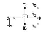
도 6a에 도시된 바와 같이, 제1 게이트전극(102,202)에 연결된 제1 게이트단자(BG)와 제2 게이트전극(118,218)에 연결된 제2 게이트단자(TG)를 연결함으로써, 하나의 게이트 신호로 제어할 수 있다. 즉, 제1 게이트단자(BG) 및 제2 게이트단자(TG)에 동일한 동작 전압(VGS)을 인가하여 메모리 박막 트랜지스터를 구동시킨다.As shown in FIG. 6A, the first gate terminal BG connected to the
이와 같이, 메모리 박막 트랜지스터에 이중 게이트 구조를 도입하고 제1 게이트전극(102,202)와 제2 게이트전극(118,218)에 동일한 동작 전압(VGS)을 인가하여 메모리 박막 트랜지스터를 구동시킴으로써, 높은 구동전류을 갖고 낮은 서브문턱전압 기울기를 가지며 높은 전계효과 이동도를 갖는 메모리 박막 트랜지스터를 제공할 수 있다. 따라서, 메모리 박막 트랜지스터의 성능을 향상시켜, 저전압 동작에 유리하고 회로의 동작속도가 증가된 메모리 소자를 제공할 수 있다.As such, by introducing a double gate structure into the memory thin film transistor and driving the memory thin film transistor by applying the same operating voltage VGS to the
도 6b는 본 발명의 일 실시예에 따른 제1 구동방법의 타이밍도를 나타내며, "VTG"는 제2 게이트전극(118,218)의 전위를 나타내고, "VBG"는 제1 게이트전극(102,202)의 전위를 나타내고, "VDS"는 드레인 전극의 전위를 나타낸다.6B illustrates a timing diagram of a first driving method according to an exemplary embodiment of the present invention, in which "VTG " represents a potential of the
메모리 박막 트랜지스터의 온 쓰기 동작(예를 들어, 데이터 "1" 저장)시, 제1 게이트전극(102,202)과 제2 게이트전극(118,218)에 소정의 양의 쓰기 전압(VGS)을 동시에 인가하고, 드레인 전압(VDS)은 접지 전압으로 고정시킨다. 이로써, 온 쓰기 동작이 완료된다.In the on-write operation of the memory thin film transistor (eg, storing data “1”), a predetermined amount of write voltage VGS is simultaneously applied to the
메모리 박막 트랜지스터의 오프 쓰기 동작(예를 들어, 데이터 "0" 저장)시, 제1 게이트전극(102,202)과 제2 게이트전극(118,218)에 소정의 음의 쓰기 전압(VGS)을 동시에 인가하고, 드레인 전압(VDS)은 접지 전압으로 고정시킨다. 이로써, 오프 쓰기 동작이 완료된다.In an off-write operation of the memory thin film transistor (eg, storing data “0”), a predetermined negative write voltage VGS is simultaneously applied to the
메모리 박막 트랜지스터에 저장된 데이터를 독출하기 위한 리드 동작시, 제1 게이트전극(102,202)과 제2 게이트전극(118,218)에 소정의 리드 전압(VGS)을 동시에 인가하고, 드레인에 소정의 드레인 전압(VDS)을 인가한다. 이때, 메모리 박막 트랜지스터를 흐르는 전류의 레벨을 검출하여 저장된 데이터를 리드한다. 본 타이밍도에서는 리드 동작시, 양의 리드 전압(VGS)을 인가하는 경우에 대해 도시하였으나, 이는 일 실시예에 불과하며, 리드 전압은 메모리 박막 트랜지스터의 동작 특성에 따라 음의 전압 또는 접지 전압으로 설정될 수도 있다.In a read operation for reading data stored in the memory thin film transistor, a predetermined read voltage VGS is simultaneously applied to the
이와 같이 이중 게이트 구조를 갖는 메모리 박막 트랜지스터에 제1 구동 방법을 적용하면, 제1 게이트절연막(104,204)과 채널막(108A,206)이 맞닿은 채널막(108A,206)의 하부 표면에 형성되는 채널층과 제2 게이트절연막(112A,212)과 채널막(108A,206)이 맞닿은 채널막(108A,206)의 상부 표면에 형성되는 채널층, 즉, 두 개의 채널층을 이용하여 메모리 박막 트랜지스터가 구동된다. 따라서, 소자의 채널 폭과 길이를 조절하지 않더라도 실효적으로 두 개의 채널층을 흐르는 드레인전류를 트랜지스터의 구동전류로 활용할 수 있다. 결과적으로, 본 발명의 이중게이트 구조를 갖는 메모리 트랜지스터는 높은 구동 전류 특성을 얻을 수 있다.When the first driving method is applied to the memory thin film transistor having the double gate structure as described above, a channel is formed on the lower surface of the
특히, 본 발명에 따르면, 소자의 크기를 결정하는 채널의 폭과 길이를 조정하지 않더라도 높은 드레인전류가 확보 가능하므로, 메모리 박막 트랜지스터의 전계효과 이동도 특성을 개선할 수 있다. 뿐만 아니라, 비교적 높은 유전율을 가지는 유기 강유전체 절연막을 제2 게이트절연막(112A,212)으로 사용함으로써, 추가적인 전계효과 이동도 개선 효과를 도모할 수 있다.In particular, according to the present invention, since the high drain current can be secured without adjusting the width and length of the channel for determining the size of the device, the field effect mobility characteristics of the memory thin film transistor can be improved. In addition, by using the organic ferroelectric insulating film having a relatively high dielectric constant as the second
물론, 본 발명의 메모리 박막 트랜지스터에 제1 구동 방법을 적용하여 확보할 수 있는 드레인 전류 값은 제1 게이트절연막(104,204) 및 제 2게이트절연막(212A,212)의 게이트 용량 값, 상기 두 개의 채널층 각각에 유기되는 전하에 의해 결정되는 문턱전압 특성에 등에 의해 결정되기 때문에, 드레인 구동전류의 최대화를 위해서는 각 소자변수를 엄밀하게 설계해야 할 필요가 있다.
Of course, the drain current values that can be obtained by applying the first driving method to the memory thin film transistor of the present invention are the gate capacitance values of the first
도 7a 및 도 7b는 본 발명의 일 실시예에 따른 이중 게이트 구조의 메모리 박막 트랜지스터의 제2 구동방법을 설명하기 위한 회로도 및 타이밍도를 나타낸다.7A and 7B illustrate a circuit diagram and a timing diagram for describing a second driving method of a memory thin film transistor having a double gate structure according to an exemplary embodiment of the present invention.
도 7a에 도시된 바와 같이, 제1 게이트전극(102,202)에 연결된 제1 게이트단자(BG) 및 제2 게이트전극(118,218)에 연결된 제2 게이트단자(TG)를 이용하여 제1 게이트전극(102,202) 및 제2 게이트전극(118,218)을 각각 제어하여, 메모리 박막 트랜지스터를 구동시킨다. 즉, 제1 게이트단자(BG) 및 제2 게이트단자(TG)에 각각 신호를 인가하여 메모리 박막 트랜지스터를 구동시킨다.As shown in FIG. 7A, the
구체적으로, 제1 게이트단자(BG)에 일정한 값을 갖는 조절전압(VBG)을 인가한 상태에서, 제2 게이트단자(TG)에 동작전압(VTG)를 인가함으로써 이중 게이트 구조의 메모리 박막 트랜지스터를 구동한다.Specifically, the memory thin film having a double gate structure by applying the operating voltage VTG to the second gate terminal TG while the control voltage VBG having a constant value is applied to the first gate terminalBG . Drive the transistor.
도 7b는 본 발명의 일 실시예에 따른 제2 구동방법의 타이밍도를 나타내며, "VTG"는 제2 게이트전극(118,218)의 전위를 나타내고, "VBG"는 제1 게이트전극(102,202)의 전위를 나타내고, "VDS"는 드레인 전극의 전위를 나타낸다.7B is a timing diagram of a second driving method according to an exemplary embodiment of the present invention, where "VTG " represents a potential of the
메모리 박막 트랜지스터의 온 쓰기 동작(예를 들어, 데이터 "1" 저장)시, 제1 게이트전극(102,202)에 소정의 음의 조절전압(VBG)이 인가된 상태에서 제2 게이트전극(118,218)에 소정의 양의 동작전압(VTG)을 인가한다. 이때, 드레인 전극은 접지시킨다. 여기서, 메모리 박막 트랜지스터의 문턱전압을 조절하기 위한 조절전압(VBG)의 크기는 메모리 트랜지스터의 동작 특성에 의해 결정된다.In the on-write operation of the memory thin film transistor (eg, storing data “1”), the
메모리 박막 트랜지스터의 오프 쓰기 동작(예를 들어, 데이터 "0"저장)시, 제1 게이트전극(102,202)에 소정의 음의 조절전압(VBG)이 인가된 상태에서 제2 게이트전극(118,218)에 소정의 음의 동작전압(VTG)을 인가한다. 이때, 드레인 전극은 접지시킨다. 여기서, 메모리 박막 트랜지스터의 문턱전압을 조절하기 위한 조절전압(VBG)의 크기는 메모리 트랜지스터의 동작 특성에 의해 결정된다.In an off-write operation of the memory thin film transistor (eg, storing data “0”), the
메모리 박막 트랜지스터에 저장된 데이터를 독출하기 위한 리드 동작시, 제1 게이트전극(102,202)에 소정의 리드전압(VTG)을 인가하고 제2 게이트전극(118,218)에 소정의 리드 전압(VGS)을 인가하고, 드레인에 소정의 드레인 전압(VDS)을 인가한다. 이때, 메모리 박막 트랜지스터를 흐르는 전류의 레벨을 검출하여 저장된 데이터를 리드한다. 본 타이밍도에서는 리드 동작시, 양의 리드 전압(VGS)을 인가하는 경우에 대해 도시하였으나, 이는 일 실시예에 불과하며, 리드 전압은 메모리 박막 트랜지스터의 동작 특성에 따라 음의 전압 또는 접지 전압으로 설정될 수도 있다.In a read operation for reading data stored in the memory thin film transistor, a predetermined read voltage VTG is applied to the
이와 같이 본 발명의 이중 게이트 구조를 갖는 메모리 박막 트랜지스터에 제2 구동방법을 적용함으로써 다음의 세 가지 효과를 기대할 수 있다.Thus, the following three effects can be expected by applying the second driving method to the memory thin film transistor having the double gate structure of the present invention.
첫 번째 효과로서, 메모리 박막 트랜지스터의 문턱전압을 소정의 범위 안에서 용이하게 제어할 수 있으며, 특히, 종래의 단일 게이트 메모리 박막 트랜지스터에 비해 문턱 전압을 높거나 낮게 설정할 수 있다.As a first effect, the threshold voltage of the memory thin film transistor can be easily controlled within a predetermined range, and in particular, the threshold voltage can be set higher or lower than that of a conventional single gate memory thin film transistor.
제1 게이트단자(BG)에 일정한 값을 갖는 조절전압(VBG)를 인가하여, 인가된 조절전압(VBG)의 전위에 따라 채널막(108A, 206)의 기본 전위를 조절할 수 있다. 예를 들어, 제1 게이트단자(BG)에 음의 조절전압(VBG)을 인가하여 메모리 박막 트랜지스터의 문턱전압을 양의 방향으로 이동시킬 수 있다. 즉, 제1 게이트 단자(BG)에 음의 값을 갖는 조절전압을 인가함으로써, 메모리 박막 트랜지스터가 양의 턴온전압을 갖도록 할 수 있다. 또한, 제1 게이트단자(BG)에 양의 조절전압(VBG)을 인가하여 메모리 박막 트랜지스터의 문턱전압을 음의 방향으로 이동시킬 수 있다.By applying a control voltage VBG having a constant value to the first gate terminalBG , the base potentials of the
따라서, 제1 게이트단자(BG)에 인가되는 조절전압(VBG)에 의해 메모리 박막 트랜지스터의 문턱전압을 용이하게 조절할 수 있다. 이때, 제1 게이트단자(BG)에 음의 조절전압(VBG)을 인가하여 메모리 박막 트랜지스터의 문턱 전압을 정전압 영역에서 형성하고, 쓰기 동작에 의한 드레인 전류의 메모리 윈도우 폭이 게이트 전압 0V를 중심으로 형성되록 함으로써, 시스템 전체의 소비전력을 감소시키고, 구동회로를 간소화하며, 데이터 리텐션 특성을 향상시킬 수 있다.Therefore, the threshold voltage of the memory thin film transistor can be easily adjusted by the control voltage VBG applied to the first gate terminal BG. At this time, a negative control voltage VBG is applied to the first gate terminal BG to form a threshold voltage of the memory thin film transistor in the constant voltage region, and the memory window width of the drain current by the write operation is centered on the
두 번째 효과로서, 메모리 박막 트랜지스터의 쓰기 속도를 향상시킬 수 있다. 유기 강유전체 박막을 게이트절연막으로 사용하는 통상의 메모리 박막 트랜지스터의 경우, 쓰기 동작에 비교적 긴 시간이 필요하다. 이는 유기 강유전체 물질의 분극 반전 속도가 특별히 느리기 때문이라기보다는, 유기 강유전체 물질의 분극 반전 속도가 인가되는 전압의 크기에 따라 크게 변화하기 때문이다. 또한, 메모리 박막 트랜지스터의 채널막이 소정의 동작전압 조건에서 완전 공핍화되어 게이트절연막의 분극 반전에 필요한 보상 전하를 채널막 내부에서 충분히 공급할 수 없기 때문인 것으로 예측할 수 있다.As a second effect, the write speed of the memory thin film transistor can be improved. In a conventional memory thin film transistor using an organic ferroelectric thin film as a gate insulating film, a relatively long time is required for a write operation. This is not because the polarization reversal rate of the organic ferroelectric material is particularly slow, but because the polarization reversal rate of the organic ferroelectric material changes greatly depending on the magnitude of the applied voltage. In addition, it can be expected that the channel film of the memory thin film transistor is completely depleted under a predetermined operating voltage condition so that the compensation charge necessary for polarization inversion of the gate insulating film cannot be sufficiently supplied inside the channel film.
따라서, 본 발명은 메모리 박막 트랜지스터의 구동시 제1 게이트전극(102,202)에 연결된 제1 게이트단자(BG)에 일정한 값을 갖는 조절전압(VBG)을 인가함으로써, 제2 게이트전극(118,218)과 채널막(108A,206) 사이의 실효적인 게이트 인가전압을 높인다. 또는, 메모리 박막 트랜지스터의 구동시 제1 게이트전극(102,202)에 연결된 제1 게이트단자(BG)에 일정한 값의 조절전압(VBG)을 인가함으로써, 제1 게이트절연막(104,204)을 통해 채널막(108A,206)에 일정량의 전하를 유기한다. 이와 같은 구동 방식을 통해, 메모리 박막 트랜지스터의 쓰기 속도를 향상시킬 수 있다.Therefore, the present invention applies the control voltage VBG having a constant value to the first gate terminal BG connected to the
세 번째 효과로서, 메모리 박막 트랜지스터 자체의 트랜지스터 성능을 더욱 향상시킬 수 있다. 본 발명에 따르면, 제1 게이트전극(102,202)에 일정한 값을 갖는 조절전압(VBG)을 인가한 상태에서 제2 게이트전극(118,218)에 동작전압(VTG)를 인가하므로, 채널막(118A,206)과 제2 게이트전극(118,218) 사이에 걸리는 실효적인 전압의 크기를 용이하게 조절할 수 있다. 따라서, 이를 이용하여 제2 게이트절연막(112A, 212)에 걸리는 전압의 크기를 용이하게 조절할 수 있으며, 이를 통해, 메모리 박막 트랜지스터의 메모리 동작마진을 더욱 크게 확보할 수 있다.As a third effect, the transistor performance of the memory thin film transistor itself can be further improved. According to the present invention, since the operating voltage VTG is applied to the
이를 위해, 제1 게이트단자(BG)에 음의 조절전압(VBG)을 인가하는 것이 바람직하며, 이를 통해, 메모리 박막 트랜지스터의 문턱전압을 양의 방향으로 이동시켜 메모리 박막 트랜지스터의 쓰기 속도를 향상시키고 메모리 박막 트랜지스터의 응용성을 더욱 향상시킬 수 있다.
To this end, it is preferable to apply a negative control voltage (VBG ) to the first gate terminal (BG), through which the threshold voltage of the memory thin film transistor is moved in the positive direction to improve the writing speed of the memory thin film transistor. In addition, the applicability of the memory thin film transistor can be further improved.
도 8a 및 도 8b는 본 발명의 일 실시예에 따라 제작된 이중 게이트 구조의 메모리 박막 트랜지스터의 게이트 전압- 드레인 전류 특성을 나타내는 그래프이다.8A and 8B are graphs illustrating gate voltage-drain current characteristics of a memory thin film transistor having a double gate structure according to an exemplary embodiment of the present invention.
여기서, 메모리 트랜지스터의 특성 측정에 사용된 소자는 앞서 설명한 제1 실시예에 따라 제조되었으며, 그 구체적인 제조 방법은 다음과 같다.Here, the device used to measure the characteristics of the memory transistor was manufactured according to the first embodiment described above, and the specific manufacturing method thereof is as follows.
기판(100)은 유리 기판을 사용하였고, 제1 게이트전극(102)는 150nm 두께의 ITO 박막을 사용하였다. 제1 게이트절연막(104)는 원자층증착법으로 형성된 65nm 두께의 알루미늄 산화막(Al2O3)을 사용하였다. 소오스 및 드레인 전극(106)은 150nm 두께의 ITO 박막을 사용하였다. 채널막(108A)은 IGZO(인듐-갈륨-아연 산화물) 박막을 스퍼터링 방법으로 형성하였으며, 막 두께는 10nm이다. 보호막(110A)은 원자층증착법으로 200oC의 온도에서 형성된 9nm 두께의 알루미늄 산화막(Al2O3)를 사용하였다. 제2 게이트절연막(112A)은 120nm 두께의 P(VDF-TrFE) 박막을 사용하였다. P(VDF-TrFE) 박막은 스핀코팅 방법을 적용하여 형성되었으며, 결정화 열처리 온도는 140oC에서 수행되었다. 콘택홀(C)의 형성 공정은 포토레지스트를 식각 마스크로 이용하는 산소 플라즈마 식각 방법으로 수행되었다. 소오스 및 드레인 전극 패드(116), 및 제2 게이트전극(118)은 알루미늄 박막으로 형성되었다.
The
도 8a는 본 발명의 제1 구동 방법에 의해 메모리 박막 트랜지스터를 구동한 경우의 동작전압에 따른 드레인 전류 측정 결과를 나타낸다.8A illustrates a drain current measurement result according to an operating voltage when the memory thin film transistor is driven by the first driving method of the present invention.
여기서, "TG"는 제2 게이트단자(TG)에만 동작전압을 인가하여 측정한 드레인전류를 나타내며, "TG/BG"는 제1 게이트단자(BG) 및 제2 게이트단자(TG)를 하나의 단자로 묶어 동시에 동작전압을 인가하여 측정한 드레인전류를 나타낸다. "log"는 측정된 드레인전류를 로그 스케일로 표시한 것이며, "linear"는 측정된 드레인 전류를 리니어 스케일로 표시한 것이다.Here, "TG" represents a drain current measured by applying an operating voltage only to the second gate terminal TG, and "TG / BG" represents one of the first gate terminal BG and the second gate terminal TG. It represents the drain current measured by applying the operating voltage at the same time. "log" shows the measured drain current on a log scale, and "linear" shows the measured drain current on a linear scale.
그래프를 통해, 제2 게이트단자(TG)만을 이용하여 메모리 박막 트랜지스터를 구동시키는 것보다 제1 게이트단자(BG) 및 제2 게이트단자(TG)를 둘다 사용하는 경우가 동일한 게이트전압, 즉, 동작전압(VTG)을 인가함에 있어서 더 큰 드레인 전류 값을 확보할 수 있음을 알 수 있다. 이는 리니어 스케일로 표시한 TG(linear) 선과 TG/BG(linear) 선을 비교하여 보다 명확히 알 수 있는데, 제2 게이트단자(TG)만을 사용한 경우에는 10V의 동작전압 인가시 약 66uA의 드레인전류를 얻을 수 있는데 비해, 제1 게이트단자(BG) 및 제2 게이트단자(TG)를 하나의 단자로 묶어 동시에 사용하는 경우에는 10V 게이트전압 인가시 약 82uA의 드레인전류를 얻을 수 있음을 알 수 있다. 결과적으로 본 발명의 이중게이트 구조를 갖는 메모리 트랜지스터의 전계효과 이동도를 개선할 수 있다.Through the graph, when both the first gate terminal BG and the second gate terminal TG are used rather than driving the memory thin film transistor using only the second gate terminal TG, that is, the operation It can be seen that a larger drain current value can be secured by applying the voltage VTG . This can be seen more clearly by comparing the TG (linear) line and the TG / BG (linear) line in linear scale. When only the second gate terminal (TG) is used, a drain current of about 66 uA is applied when an operating voltage of 10 V is applied. In contrast, when the first gate terminal BG and the second gate terminal TG are bundled and used simultaneously, a drain current of about 82 uA can be obtained when a 10 V gate voltage is applied. As a result, the field effect mobility of the memory transistor having the double gate structure of the present invention can be improved.
따라서, 본 발명에 따르면, 메모리 박막 트랜지스터에 이중 게이트 구조를 도입함으로써 동일한 동작전압을 이용하여 더 큰 드레인 전류값을 확보할 수 있음을 확인하였다.
Therefore, according to the present invention, it was confirmed that by introducing a double gate structure in the memory thin film transistor, a larger drain current value can be obtained using the same operating voltage.
도 8b는 본 발명의 제2 구동방법에 의해 메모리 박막 트랜지스터를 구동한 경우의 동작전압에 따른 드레인 전류 측정 결과를 나타낸다.8B illustrates a drain current measurement result according to an operating voltage when the memory thin film transistor is driven by the second driving method of the present invention.
여기서, 각 데이터 라인은 제1 게이트단자(BG)에 -6V, -2V, 0V, 2V, 6V의 조절전압(VBG)을 인가한 상태에서 제2 게이트단자(TG)에 -14 내지 10V의 범위의 동작전압(VTG)을 인가하였을 때 얻어진 드레인전류 값의 변화를 나타낸 것이다.Here, each data line has a voltage of -14 to 10V at the second gate terminal TG while the control voltages VBG of -6V, -2V, 0V, 2V, and 6V are applied to the first gate terminalBG . The change of the drain current obtained when the operating voltage (VTG ) of the range is applied is shown.
그래프를 통해, 제2 게이트단자(TG)에 인가되는 게이트 전압, 즉, 동작전압(VTG)의 인가 영역이 -14 내지 10V로 동일하더라도, 제1 게이트단자(BG)에 인가되는 조절전압(VBG)의 레벨에 따라 메모리 박막 트랜지스터의 문턱전압을 제어할 수 있음을 알 수 있다. 보다 구체적으로는 제1 게이트단자(BG)에 양의 조절전압(VBG)을 인가시켜 메모리 박막 트랜지스터의 문턱전압을 음의 방향으로 이동시키거나(가는 실선, 일점 쇄선 참조), 제1 게이트단자(BG)에 음의 조절전압(VBG)을 인가시켜 메모리 박막 트랜지스터의 문턱전압을 양의 방향으로 이동(이점 쇄선, 굵은 실선 참조)시킬 수 있음을 알 수 있다.Through the graph, even if the application region of the gate voltage applied to the second gate terminal TG, that is, the operating voltage VTG is equal to −14 to 10V, the control voltage applied to the first gate terminal BG ( It can be seen that the threshold voltage of the memory thin film transistor can be controlled according to the level of VBG ). More specifically, by applying a positive control voltage (VBG ) to the first gate terminal (BG) to move the threshold voltage of the memory thin film transistor in the negative direction (refer to the solid line, one-dot chain line), or the first gate terminal It can be seen that the threshold voltage of the memory thin film transistor can be shifted in a positive direction (see a dashed-dotted line and a thick solid line) by applying a negative control voltage VBG to (BG ).
따라서, 본 발명에 따르면, 제1 게이트전극(102,202)에 인가되는 조절전압(VBG)에 의해 메모리 박막 트랜지스터의 문턱전압을 용이하게 조절할 수 있음을 확인하였다.
Therefore, according to the present invention, it can be seen that the threshold voltage of the memory thin film transistor can be easily adjusted by the control voltage VBG applied to the
본 발명의 기술 사상은 상기 바람직한 실시예들에 따라 구체적으로 기록되었으나, 상기한 실시예는 그 설명을 위한 것이며 그 제한을 위한 것이 아님을 주의하여야 한다. 또한, 본 발명의 기술 분야의 통상의 전문가라면 본 발명의 기술 사상의 범위 내에서 다양한 실시예가 가능함을 이해할 수 있을 것이다.
Although the technical spirit of the present invention has been specifically recorded in accordance with the above-described preferred embodiments, it should be noted that the above-described embodiment is for the purpose of description and not of limitation. In addition, it will be understood by those of ordinary skill in the art that various embodiments are possible within the scope of the technical idea of the present invention.
100: 기판102: 제1 게이트전극
104: 제1 게이트절연막106: 소오스 및 드레인 전극
108: 채널용 물질막108A: 채널막
110: 보호용 물질막110A: 보호막
112,112A: 제2 게이트절연막114: 콘택플러그
116: 소오스 및 드레인 전극 패드118: 제2 게이트전극
200: 기판202: 제1 게이트전극
204: 제1 게이트절연막206: 채널막
208: 보호막210: 소오스 및 드레인 전극
212: 제2 게이트절연막214: 콘택플러그
216: 소오스 및 드레인 전극 패드218: 제2 게이트전극
BG: 제1 게이트단자TG: 제2 게이트단자100: substrate 102: first gate electrode
104: first gate insulating film 106: source and drain electrodes
108:
110:
112, 112A: second gate insulating film 114: contact plug
116: source and drain electrode pad 118: second gate electrode
200: substrate 202: first gate electrode
204: first gate insulating film 206: channel film
208: protective film 210: source and drain electrodes
212: second gate insulating film 214: contact plug
216: source and drain electrode pad 218: second gate electrode
BG: first gate terminal TG: second gate terminal
Claims (13)
Translated fromKorean상기 제1 게이트전극 상에 형성된 제1 게이트절연막;
상기 제1 게이트절연막 상에 소정 간격으로 형성된 소오스 및 드레인 전극;
상기 소오스 및 드레인 전극 사이의 상기 제1게이트 절연막 상에 형성된 채널막;
상기 채널막 상에 형성된 제2 게이트절연막; 및
상기 제2 게이트절연막 상에 형성되며, 상기 제1 게이트전극과 연결되어 상기 동작전압이 인가되는 제2 게이트전극
을 포함하는 이중 게이트 구조의 비휘발성 메모리 트랜지스터.
A first gate electrode formed on the substrate and to which an operating voltage is applied;
A first gate insulating film formed on the first gate electrode;
Source and drain electrodes formed on the first gate insulating layer at predetermined intervals;
A channel film formed on the first gate insulating film between the source and drain electrodes;
A second gate insulating film formed on the channel film; And
A second gate electrode formed on the second gate insulating layer and connected to the first gate electrode to apply the operating voltage;
Non-volatile memory transistor of a double gate structure comprising a.
온 쓰기 동작시,
상기 제1 게이트전극 및 상기 제2 게이트전극에 양의 쓰기 전압이 인가되는
이중 게이트 구조의 비휘발성 메모리 트랜지스터.
The method of claim 1,
On write operation,
A positive write voltage is applied to the first gate electrode and the second gate electrode.
Non-volatile memory transistor with double gate structure.
오프 쓰기 동작시,
상기 제1 게이트전극 및 상기 제2 게이트전극에 음의 쓰기 전압이 인가되는
이중 게이트 구조의 비휘발성 메모리 트랜지스터.
The method of claim 1,
In the off-write operation,
A negative write voltage is applied to the first gate electrode and the second gate electrode.
Non-volatile memory transistor with double gate structure.
상기 제1 게이트전극 상에 형성된 제1 게이트절연막;
상기 제1 게이트절연막 상에 소정 간격으로 형성된 소오스 및 드레인 전극;
상기 소오스 및 드레인 전극 사이의 상기 제1게이트 절연막 상에 형성된 채널막;
상기 채널막 상에 형성된 제2 게이트절연막; 및
상기 제2 게이트절연막 상에 형성되며, 상기 제1 게이트전극에 상기 조절전압이 인가된 상태에서 동작전압이 인가되는 제2 게이트전극
을 포함하는 이중 게이트 구조의 비휘발성 메모리 트랜지스터.
A first gate electrode formed on the substrate and to which a control voltage for adjusting a threshold voltage of the transistor is applied;
A first gate insulating film formed on the first gate electrode;
Source and drain electrodes formed on the first gate insulating layer at predetermined intervals;
A channel film formed on the first gate insulating film between the source and drain electrodes;
A second gate insulating film formed on the channel film; And
A second gate electrode formed on the second gate insulating layer and to which an operating voltage is applied while the control voltage is applied to the first gate electrode;
Non-volatile memory transistor of a double gate structure comprising a.
상기 제1 게이트 전극에 음의 값을 갖는 상기 조절전압이 인가되며, 상기 비휘발성 메모리 트랜지스터는 양의 턴온전압을 갖는
이중 게이트 구조의 비휘발성 메모리 트랜지스터.
The method of claim 4, wherein
The control voltage having a negative value is applied to the first gate electrode, and the nonvolatile memory transistor has a positive turn-on voltage.
Non-volatile memory transistor with double gate structure.
온 쓰기 동작시,
상기 제1 게이트전극에 음의 조절전압이 인가된 상태에서 상기 제2 게이트전극에 양의 쓰기 전압이 인가되는
이중 게이트 구조의 비휘발성 메모리 트랜지스터.
The method of claim 4, wherein
On write operation,
A positive write voltage is applied to the second gate electrode while a negative control voltage is applied to the first gate electrode.
Non-volatile memory transistor with double gate structure.
오프 쓰기 동작시,
상기 제1 게이트전극에 음의 조절전압이 인가된 상태에서 상기 제2 게이트전극에 음의 쓰기 전압이 인가되는
이중 게이트 구조의 비휘발성 메모리 트랜지스터.
The method of claim 4, wherein
In the off-write operation,
A negative write voltage is applied to the second gate electrode while a negative control voltage is applied to the first gate electrode.
Non-volatile memory transistor with double gate structure.
리드 동작시,
상기 제1 게이트전극에 음의 조절전압이 인가된 상태에서 상기 제2 게이트전극에 리드 전압이 인가되는
이중 게이트 구조의 비휘발성 메모리 트랜지스터.
The method of claim 4, wherein
In lead operation,
A read voltage is applied to the second gate electrode while a negative control voltage is applied to the first gate electrode.
Non-volatile memory transistor with double gate structure.
상기 채널막은 가시광 영역에서 투명한 산화물 반도체로 형성된
이중 게이트 구조의 비휘발성 메모리 트랜지스터.
The method according to claim 1 or 4,
The channel film is formed of an oxide semiconductor transparent in the visible light region.
Non-volatile memory transistor with double gate structure.
상기 제2 게이트절연막은 유기 강유전체로 형성된
이중 게이트 구조의 비휘발성 메모리 트랜지스터.
The method according to claim 1 or 4,
The second gate insulating film is formed of an organic ferroelectric
Non-volatile memory transistor with double gate structure.
상기 채널막 상에 형성된 보호막
을 더 포함하는 이중 게이트 구조의 비휘발성 메모리 트랜지스터.
The method according to claim 1 or 4,
A protective film formed on the channel film
The non-volatile memory transistor of the dual gate structure further comprising.
상기 채널막은,
상기 소오스 및 드레인 전극의 측벽 및 상부 일부를 덮는
이중 게이트 구조의 비휘발성 메모리 트랜지스터.
The method according to claim 1 or 4,
The channel film,
Covering sidewalls and upper portions of the source and drain electrodes;
Non-volatile memory transistor with double gate structure.
상기 소오스 및 드레인 전극은,
상기 채널막의 측벽 및 상부 일부를 덮는
이중 게이트 구조의 비휘발성 메모리 트랜지스터.The method according to claim 1 or 4,
The source and drain electrodes,
Covering sidewalls and upper portions of the channel layer;
Non-volatile memory transistor with double gate structure.
Priority Applications (2)
| Application Number | Priority Date | Filing Date | Title |
|---|---|---|---|
| KR1020100066837AKR20120006218A (en) | 2010-07-12 | 2010-07-12 | Double Gate Nonvolatile Memory Transistor |
| US13/173,625US20120007158A1 (en) | 2010-07-12 | 2011-06-30 | Non-volatile memory transistor having double gate structure |
Applications Claiming Priority (1)
| Application Number | Priority Date | Filing Date | Title |
|---|---|---|---|
| KR1020100066837AKR20120006218A (en) | 2010-07-12 | 2010-07-12 | Double Gate Nonvolatile Memory Transistor |
Publications (1)
| Publication Number | Publication Date |
|---|---|
| KR20120006218Atrue KR20120006218A (en) | 2012-01-18 |
Family
ID=45437973
Family Applications (1)
| Application Number | Title | Priority Date | Filing Date |
|---|---|---|---|
| KR1020100066837ACeasedKR20120006218A (en) | 2010-07-12 | 2010-07-12 | Double Gate Nonvolatile Memory Transistor |
Country Status (2)
| Country | Link |
|---|---|
| US (1) | US20120007158A1 (en) |
| KR (1) | KR20120006218A (en) |
Cited By (9)
| Publication number | Priority date | Publication date | Assignee | Title |
|---|---|---|---|---|
| KR101355624B1 (en)* | 2012-06-25 | 2014-01-27 | 인텔렉추얼디스커버리 주식회사 | A transparent and flexible non-volatile memory cell with common oxide semiconductor channel and manufacturing method for the same |
| US9412769B2 (en) | 2013-08-05 | 2016-08-09 | Samsung Electronics Co., Ltd. | Transistor, method of manufacturing the transistor, and electronic device including the transistor |
| KR20180136324A (en)* | 2017-06-14 | 2018-12-24 | 광운대학교 산학협력단 | High Performance Solution-Processed Zinc-Tin-Oxide Thin-Film Transistors Employing Ferroelectric Copolymers Fabricated at Low Temperature for Transparent Flexible Displays and encapsulation process method of ZTO TFT device using fluoroploymer thin film |
| KR20200045180A (en)* | 2018-10-22 | 2020-05-04 | 경희대학교 산학협력단 | Non-volatile memory device and method for fabricating the same |
| KR20210085930A (en)* | 2019-12-31 | 2021-07-08 | 에스케이하이닉스 주식회사 | non volatile memory device having resistance change layer and method of operating non volatile memory device |
| CN113380822A (en)* | 2020-05-29 | 2021-09-10 | 台湾积体电路制造股份有限公司 | Memory cell, semiconductor device and forming method thereof |
| US11710790B2 (en) | 2020-05-29 | 2023-07-25 | Taiwan Semiconductor Manufacturing Company, Ltd. | Memory array channel regions |
| US12051750B2 (en) | 2020-05-29 | 2024-07-30 | Taiwan Semiconductor Manufacturing Co., Ltd. | Memory array gate structures |
| US12219777B2 (en) | 2020-06-30 | 2025-02-04 | Taiwan Semiconductor Manufacturing Company, Ltd | Memory array source/drain electrode structures |
Families Citing this family (22)
| Publication number | Priority date | Publication date | Assignee | Title |
|---|---|---|---|---|
| JP6226518B2 (en)* | 2011-10-24 | 2017-11-08 | 株式会社半導体エネルギー研究所 | Semiconductor device |
| CN102651401B (en)* | 2011-12-31 | 2015-03-18 | 京东方科技集团股份有限公司 | A kind of thin film transistor, array substrate and its manufacturing method and display device |
| KR20140106977A (en)* | 2013-02-27 | 2014-09-04 | 삼성전자주식회사 | Metal oxide semiconductor Thin Film Transistors having high performance and methods of manufacturing the same |
| TWI742574B (en) | 2013-05-16 | 2021-10-11 | 日商半導體能源研究所股份有限公司 | Semiconductor device |
| TWI624936B (en) | 2013-06-05 | 2018-05-21 | 半導體能源研究所股份有限公司 | Display device |
| US10242989B2 (en)* | 2014-05-20 | 2019-03-26 | Micron Technology, Inc. | Polar, chiral, and non-centro-symmetric ferroelectric materials, memory cells including such materials, and related devices and methods |
| KR102312924B1 (en) | 2015-04-08 | 2021-10-14 | 삼성디스플레이 주식회사 | Thin film transistor display panel and manufacturing method thereof |
| CN105390451B (en)* | 2015-12-03 | 2018-03-30 | 深圳市华星光电技术有限公司 | The preparation method of low temperature polycrystalline silicon TFT substrate |
| US10161901B2 (en) | 2015-12-07 | 2018-12-25 | Taiwan Semiconductor Manufacturing Co., Ltd. | Dual gate biologically sensitive field effect transistor |
| JP6698486B2 (en)* | 2016-09-26 | 2020-05-27 | 株式会社ジャパンディスプレイ | Display device |
| US10340903B2 (en) | 2016-11-24 | 2019-07-02 | Electronics & Telecommunications Research Institute | Semiconductor device and operation method thereof |
| US10937807B2 (en) | 2016-12-29 | 2021-03-02 | Intel Corporation | Ferroelectric field-effect transistor devices having a top gate and a bottom gate |
| CN108281488B (en)* | 2018-01-03 | 2021-07-27 | 京东方科技集团股份有限公司 | Array substrate, preparation method thereof and display device |
| KR20210033346A (en)* | 2019-09-18 | 2021-03-26 | 삼성전자주식회사 | Electronic device and method of manufacturing the same |
| US11710775B2 (en) | 2020-05-29 | 2023-07-25 | Taiwan Semiconductor Manufacturing Co., Ltd. | Ferroelectric field effect transistor |
| US12382640B2 (en) | 2020-10-30 | 2025-08-05 | Taiwan Semiconductor Manufacturing Company, Ltd. | Memory device and method for fabricating the same |
| US11706928B2 (en)* | 2020-10-30 | 2023-07-18 | Taiwan Semiconductor Manufacturing Company, Ltd. | Memory device and method for fabricating the same |
| JP7491815B2 (en)* | 2020-11-12 | 2024-05-28 | ルネサスエレクトロニクス株式会社 | Method for manufacturing semiconductor device |
| CN112735272B (en)* | 2020-12-30 | 2022-05-17 | 武汉华星光电技术有限公司 | Display panel and display device |
| JP2023028988A (en)* | 2021-08-20 | 2023-03-03 | 株式会社ジャパンディスプレイ | transistor |
| US11646376B2 (en)* | 2021-09-20 | 2023-05-09 | Renesas Electronics Corporation | Semiconductor device and method of manufacturing the same |
| CN115132764B (en)* | 2021-12-09 | 2025-03-11 | 友达光电股份有限公司 | Active component substrate and manufacturing method thereof |
Family Cites Families (6)
| Publication number | Priority date | Publication date | Assignee | Title |
|---|---|---|---|---|
| JP3214715B2 (en)* | 1991-10-25 | 2001-10-02 | ローム株式会社 | Semiconductor storage element |
| JP2004039965A (en)* | 2002-07-05 | 2004-02-05 | Renesas Technology Corp | Nonvolatile semiconductor memory device |
| US7297977B2 (en)* | 2004-03-12 | 2007-11-20 | Hewlett-Packard Development Company, L.P. | Semiconductor device |
| KR101270172B1 (en)* | 2007-08-29 | 2013-05-31 | 삼성전자주식회사 | Oxide thin film transistor and manufacturing method for the same |
| US8004871B2 (en)* | 2008-05-26 | 2011-08-23 | Panasonic Corporation | Semiconductor memory device including FET memory elements |
| US20110170330A1 (en)* | 2008-09-23 | 2011-07-14 | National University Of Singapore | Graphene Memory Cell and Fabrication Methods Thereof |
- 2010
- 2010-07-12KRKR1020100066837Apatent/KR20120006218A/ennot_activeCeased
- 2011
- 2011-06-30USUS13/173,625patent/US20120007158A1/ennot_activeAbandoned
Cited By (12)
| Publication number | Priority date | Publication date | Assignee | Title |
|---|---|---|---|---|
| KR101355624B1 (en)* | 2012-06-25 | 2014-01-27 | 인텔렉추얼디스커버리 주식회사 | A transparent and flexible non-volatile memory cell with common oxide semiconductor channel and manufacturing method for the same |
| US9412769B2 (en) | 2013-08-05 | 2016-08-09 | Samsung Electronics Co., Ltd. | Transistor, method of manufacturing the transistor, and electronic device including the transistor |
| KR20180136324A (en)* | 2017-06-14 | 2018-12-24 | 광운대학교 산학협력단 | High Performance Solution-Processed Zinc-Tin-Oxide Thin-Film Transistors Employing Ferroelectric Copolymers Fabricated at Low Temperature for Transparent Flexible Displays and encapsulation process method of ZTO TFT device using fluoroploymer thin film |
| KR20200045180A (en)* | 2018-10-22 | 2020-05-04 | 경희대학교 산학협력단 | Non-volatile memory device and method for fabricating the same |
| KR20210085930A (en)* | 2019-12-31 | 2021-07-08 | 에스케이하이닉스 주식회사 | non volatile memory device having resistance change layer and method of operating non volatile memory device |
| CN113380822A (en)* | 2020-05-29 | 2021-09-10 | 台湾积体电路制造股份有限公司 | Memory cell, semiconductor device and forming method thereof |
| KR20210148868A (en)* | 2020-05-29 | 2021-12-08 | 타이완 세미콘덕터 매뉴팩쳐링 컴퍼니 리미티드 | Memory array channel regions |
| US11710790B2 (en) | 2020-05-29 | 2023-07-25 | Taiwan Semiconductor Manufacturing Company, Ltd. | Memory array channel regions |
| US12051750B2 (en) | 2020-05-29 | 2024-07-30 | Taiwan Semiconductor Manufacturing Co., Ltd. | Memory array gate structures |
| CN113380822B (en)* | 2020-05-29 | 2024-12-27 | 台湾积体电路制造股份有限公司 | Memory cell, semiconductor device and method for forming the same |
| US12272750B2 (en) | 2020-05-29 | 2025-04-08 | Taiwan Semiconductor Manufacturing Co., Ltd. | Memory array channel regions |
| US12219777B2 (en) | 2020-06-30 | 2025-02-04 | Taiwan Semiconductor Manufacturing Company, Ltd | Memory array source/drain electrode structures |
Also Published As
| Publication number | Publication date |
|---|---|
| US20120007158A1 (en) | 2012-01-12 |
Similar Documents
| Publication | Publication Date | Title |
|---|---|---|
| KR20120006218A (en) | Double Gate Nonvolatile Memory Transistor | |
| JP5417275B2 (en) | Nonvolatile memory cell and manufacturing method thereof | |
| US8188472B2 (en) | Thin film transistor, method of manufacturing the same, and flat panel display having the same | |
| US8476106B2 (en) | Transparent nonvolatile memory thin film transistor and method of manufacturing the same | |
| KR100963026B1 (en) | Thin film transistor, its manufacturing method, and flat panel display device comprising thin film transistor | |
| US8178884B2 (en) | Thin film transistor including compound semiconductor oxide, method of manufacturing the same and flat panel display device having the same | |
| US9048163B2 (en) | Transistor, electronic device including transistor, and manufacturing methods thereof | |
| US9123817B2 (en) | Transistors and electronic devices including the same | |
| US11011534B2 (en) | Multi-level cell thin-film transistor memory and method of fabricating the same | |
| US8497506B2 (en) | Protecting semiconducting oxides | |
| KR101238823B1 (en) | The thin film transistor and the manufacuring method thereof | |
| KR101638977B1 (en) | Transistor, method of manufacturing the same and electronic device comprising transistor | |
| JP2006121029A (en) | Solid state electronic equipment | |
| CN104347813B (en) | Transistor, the method for manufacturing transistor and the electronic device including transistor | |
| CN1376311A (en) | Ferroelectric transistor | |
| KR20100135544A (en) | Transistors, manufacturing methods thereof, and electronic devices including the transistors | |
| KR101343569B1 (en) | Non-volatile memory cell and method for manufacturing the same | |
| KR101268696B1 (en) | Method of manufacturing non-volatile memory device using transparent substrate or flexible substrates | |
| KR20110010019A (en) | Method for manufacturing a transparent or flexible nonvolatile memory device using a transparent substrate or a flexible substrate | |
| US20150194530A1 (en) | Thin film transistor and method of manufacturing the same | |
| JP2010062221A (en) | Ferroelectric gate field effect transistor, memory element using the same, and method of manufacturing the ferroelectric gate field effect transistor | |
| EP1168454B1 (en) | Nonvolatile semiconductor memory | |
| KR101040137B1 (en) | Thin film transistor using asymmetric electrode structure and manufacturing method thereof | |
| CN111129150A (en) | A kind of ferroelectric thin film transistor and its manufacturing method | |
| KR20190106320A (en) | Flexible Nonvolatile Memory using Vapor Deposition Polymer Insulating Layer |
Legal Events
| Date | Code | Title | Description |
|---|---|---|---|
| A201 | Request for examination | ||
| PA0109 | Patent application | Patent event code:PA01091R01D Comment text:Patent Application Patent event date:20100712 | |
| PA0201 | Request for examination | ||
| PG1501 | Laying open of application | ||
| E902 | Notification of reason for refusal | ||
| PE0902 | Notice of grounds for rejection | Comment text:Notification of reason for refusal Patent event date:20130724 Patent event code:PE09021S01D | |
| E601 | Decision to refuse application | ||
| PE0601 | Decision on rejection of patent | Patent event date:20140226 Comment text:Decision to Refuse Application Patent event code:PE06012S01D Patent event date:20130724 Comment text:Notification of reason for refusal Patent event code:PE06011S01I |