KR20120006096A - Optical module and manufacturing method - Google Patents
Optical module and manufacturing methodDownload PDFInfo
- Publication number
- KR20120006096A KR20120006096AKR1020120000554AKR20120000554AKR20120006096AKR 20120006096 AKR20120006096 AKR 20120006096AKR 1020120000554 AKR1020120000554 AKR 1020120000554AKR 20120000554 AKR20120000554 AKR 20120000554AKR 20120006096 AKR20120006096 AKR 20120006096A
- Authority
- KR
- South Korea
- Prior art keywords
- optical
- substrate
- optical fiber
- device chip
- cover
- Prior art date
- Legal status (The legal status is an assumption and is not a legal conclusion. Google has not performed a legal analysis and makes no representation as to the accuracy of the status listed.)
- Granted
Links
Images


Classifications
- G—PHYSICS
- G02—OPTICS
- G02B—OPTICAL ELEMENTS, SYSTEMS OR APPARATUS
- G02B6/00—Light guides; Structural details of arrangements comprising light guides and other optical elements, e.g. couplings
- G02B6/24—Coupling light guides
- G02B6/42—Coupling light guides with opto-electronic elements
- G02B6/4201—Packages, e.g. shape, construction, internal or external details
- G02B6/4274—Electrical aspects
- G02B6/428—Electrical aspects containing printed circuit boards [PCB]
- G—PHYSICS
- G02—OPTICS
- G02B—OPTICAL ELEMENTS, SYSTEMS OR APPARATUS
- G02B6/00—Light guides; Structural details of arrangements comprising light guides and other optical elements, e.g. couplings
- G02B6/10—Light guides; Structural details of arrangements comprising light guides and other optical elements, e.g. couplings of the optical waveguide type
- G02B6/12—Light guides; Structural details of arrangements comprising light guides and other optical elements, e.g. couplings of the optical waveguide type of the integrated circuit kind
- G02B6/122—Basic optical elements, e.g. light-guiding paths
- G02B6/1228—Tapered waveguides, e.g. integrated spot-size transformers
- G—PHYSICS
- G02—OPTICS
- G02B—OPTICAL ELEMENTS, SYSTEMS OR APPARATUS
- G02B6/00—Light guides; Structural details of arrangements comprising light guides and other optical elements, e.g. couplings
- G02B6/24—Coupling light guides
- G02B6/42—Coupling light guides with opto-electronic elements
- G02B6/4201—Packages, e.g. shape, construction, internal or external details
- G02B6/4204—Packages, e.g. shape, construction, internal or external details the coupling comprising intermediate optical elements, e.g. lenses, holograms
- G—PHYSICS
- G02—OPTICS
- G02B—OPTICAL ELEMENTS, SYSTEMS OR APPARATUS
- G02B6/00—Light guides; Structural details of arrangements comprising light guides and other optical elements, e.g. couplings
- G02B6/24—Coupling light guides
- G02B6/42—Coupling light guides with opto-electronic elements
- G02B6/4201—Packages, e.g. shape, construction, internal or external details
- G02B6/4219—Mechanical fixtures for holding or positioning the elements relative to each other in the couplings; Alignment methods for the elements, e.g. measuring or observing methods especially used therefor
- G02B6/4236—Fixing or mounting methods of the aligned elements
- G02B6/4239—Adhesive bonding; Encapsulation with polymer material
- G—PHYSICS
- G02—OPTICS
- G02B—OPTICAL ELEMENTS, SYSTEMS OR APPARATUS
- G02B6/00—Light guides; Structural details of arrangements comprising light guides and other optical elements, e.g. couplings
- G02B6/24—Coupling light guides
- G02B6/42—Coupling light guides with opto-electronic elements
- G02B6/4201—Packages, e.g. shape, construction, internal or external details
- G02B6/4249—Packages, e.g. shape, construction, internal or external details comprising arrays of active devices and fibres
Landscapes
- Physics & Mathematics (AREA)
- General Physics & Mathematics (AREA)
- Optics & Photonics (AREA)
- Engineering & Computer Science (AREA)
- Power Engineering (AREA)
- Microelectronics & Electronic Packaging (AREA)
- Optical Couplings Of Light Guides (AREA)
Abstract
Description
Translated fromKorean본 발명은 광 모듈 및 그 제조방법에 관한 것으로, 보다 상세하게는 소형화가 가능하고, 대량 생산으로 단가를 줄일 수 있을 뿐만 아니라 다양한 형태의 광 송수신모듈 및 패키징(Packaging)이 가능하도록한 광 모듈 및 그 제조방법에 관한 것이다.
The present invention relates to an optical module and a method of manufacturing the same, and more particularly, to reduce the size, to reduce the unit cost by mass production, and to enable various types of optical transmission and reception module and packaging (Packaging) and It relates to a manufacturing method.
정보화시대가 도래하면서 많은 양의 정보를 전송할 수 있는 광을 이용한 광 모듈에 대한 필요성이 제기되고 있다. 그 중에서 광을 이용한 광 모듈은 모듈 자체가 가지고 있는 특성이 우수하여야 할 뿐만 아니라 오랜 시간 동안 자체의 특성을 유지해야 하는 높은 신뢰성이 요구된다.With the advent of the information age, there is a need for an optical module using light capable of transmitting a large amount of information. Among them, the optical module using light is required to have a high reliability of not only having excellent characteristics of the module itself but also maintaining its characteristics for a long time.
FTTH(Fiber To The Home)의 구현을 위한 광 모듈의 보급을 촉진하기 위해서는 저렴한 가격이 유지되어야만 한다. 특히, 광 전송시스템의 용량이 커짐에 따라 광 전송시스템에 탑재되는 광 모듈의 크기를 줄여 단위 면적 당 탑재할 수 있는 모듈의 수량을 늘이려는 노력이 계속적으로 진행되고 있다.Low prices must be maintained to facilitate the dissemination of optical modules for the implementation of Fiber To The Home (FTTH). In particular, as the capacity of the optical transmission system increases, efforts have been made to increase the number of modules that can be mounted per unit area by reducing the size of the optical module mounted in the optical transmission system.
한편, 기존의 광 모듈로는 플랫폼(Platform) 형태의 기판 상면에 광소자 및 전자소자를 집적하여 금속 케이스(case)에 집어넣은 버터플라이(Butterfly) 구조와, 광 송신 및 수신 등의 기능을 수행할 수 있는 능동 소자(예를 들면, 포토 다이오드나 레이저 다이오드 등)들이 집적된 스템 상면을 덮는 티오 캔(TO-CAN) 구조 등이 있다.Meanwhile, the existing optical module performs a function of a butterfly structure in which an optical device and an electronic device are integrated on a platform-type substrate and inserted into a metal case, and transmit and receive light. There is a thio-can (TO-CAN) structure that covers the upper surface of the stem in which the active devices (for example, photodiode or laser diode, etc.) that can be integrated.
상기 티오 캔(TO-CAN) 구조를 갖는 광 모듈은 그 제작 단가가 낮아서, 다양한 형태의 초고속 광통신 시스템에 널리 적용되고 있지만, 티오 캔(TO-CAN) 패키지 자체의 부피를 줄이는데 한계가 있어 광 모듈의 소형화를 위해서는 새로운 구조의 광 모듈이 필요하다.
The optical module having the thio-can (TO-CAN) structure is low manufacturing cost, widely applied to various types of high-speed optical communication system, but there is a limit in reducing the volume of the thio-can (TO-CAN) package itself optical module In order to miniaturize, a new optical module is required.
본 발명은 전술한 문제점을 해결하기 위하여 안출된 것으로서, 본 발명의 목적은 소형화가 가능하고, 대량 생산으로 단가를 줄일 수 있을 뿐만 아니라 다양한 형태의 광 송수신모듈 및 패키징(Packaging)이 가능하도록 한 광 모듈 및 그 제조방법을 제공하는데 있다.
The present invention has been made to solve the above-described problems, the object of the present invention is to reduce the unit cost, and to reduce the unit cost as well as mass production of optical transmission and reception module and packaging (Packaging) It is to provide a module and a method of manufacturing the same.
전술한 목적을 달성하기 위하여 본 발명의 제1 측면은, 상부에 광소자 칩이 구비된 기판; 적어도 하나의 관통홀이 형성되며, 상기 관통홀에 상기 광소자 칩이 삽입되도록 상기 기판 상에 결합되는 스페이서; 상기 관통홀을 폐쇄하도록 상기 스페이서 상에 결합되는 덮개; 및 상기 덮개 상에 상기 광소자 칩의 위치와 대응되도록 결합되는 광섬유를 포함하며, 상기 광섬유를 통해 전달되는 빛을 상기 광소자 칩으로 입사시키거나, 상기 광소자 칩에서 방출되는 빛을 상기 광섬유로 입사시키도록 구성된 것을 특징으로 하는 광 모듈을 제공하는 것이다.In order to achieve the above object, the first aspect of the present invention, the optical device chip is provided on the top; At least one through hole formed on the substrate and coupled to the substrate such that the optical device chip is inserted into the through hole; A cover coupled to the spacer to close the through hole; And an optical fiber coupled to the position of the optical device chip on the cover, and incident light transmitted through the optical fiber to the optical device chip, or light emitted from the optical device chip to the optical fiber. To provide an optical module, characterized in that configured to be incident.
여기서, 상기 기판 상에 상기 광소자 칩과 전기적으로 접속되도록 전극패턴이 더 형성됨이 바람직하다.Here, it is preferable that an electrode pattern is further formed on the substrate to be electrically connected to the optical device chip.
바람직하게, 상기 전극패턴에 전기적으로 접속되도록 전자소자 칩이 더 구비되되, 상기 전자소자 칩은 상기 광소자 칩의 하부 또는 주변에 구비될 수 있다.Preferably, an electronic device chip is further provided to be electrically connected to the electrode pattern, and the electronic device chip may be provided below or around the optical device chip.
바람직하게, 상기 기판의 적어도 일 측면은 상기 스페이서의 측면 외측으로 돌출 형성될 수 있다.Preferably, at least one side of the substrate may protrude to the outside of the side of the spacer.
바람직하게, 상기 광섬유는 상기 덮개 상에 투명한 에폭시를 통해 고정 결합될 수 있다.Preferably, the optical fiber may be fixedly coupled through a transparent epoxy on the cover.
바람직하게, 상기 덮개의 상면 및 하면에 무반사 광학 코팅층이 더 형성될 수 있다.Preferably, the anti-reflective optical coating layer may be further formed on the upper and lower surfaces of the cover.
바람직하게, 상기 덮개의 상면 또는 하면에 상기 광섬유의 결합 위치와 대응되도록 렌즈가 더 형성되되, 상기 렌즈가 상기 덮개의 상면에 형성될 경우, 상기 렌즈와 상기 광섬유간에 일정간격 이격되도록 투명한 에폭시를 통해 고정 결합될 수 있다.Preferably, the lens is further formed on the upper or lower surface of the cover to correspond to the coupling position of the optical fiber, when the lens is formed on the upper surface of the cover, through a transparent epoxy to be spaced apart a predetermined distance between the lens and the optical fiber Can be fixedly coupled.
바람직하게, 상기 덮개의 상면 또는 하면에 상기 광섬유의 결합 위치와 대응되도록 일정각도의 경사면을 갖는 요홈부 또는 돌출부가 더 형성될 수 있다.Preferably, a groove or a protrusion having an inclined surface at an angle may be further formed on the top or bottom of the cover to correspond to the coupling position of the optical fiber.
바람직하게, 상기 요홈부 또는 돌출부가 형성되는 반대면에 상기 광섬유의 결합 위치와 대응되도록 렌즈가 더 형성되되, 상기 렌즈가 상기 덮개의 상면에 형성될 경우, 상기 렌즈와 상기 광섬유간에 일정간격 이격되도록 투명한 에폭시를 통해 고정 결합될 수 있다.Preferably, the lens is further formed to correspond to the coupling position of the optical fiber on the opposite surface on which the groove portion or the projection is formed, so that when the lens is formed on the upper surface of the cover, a predetermined distance between the lens and the optical fiber It can be fixedly bonded through the transparent epoxy.
바람직하게, 별도의 회로기판에 상기 기판을 표면 실장하여 상기 회로기판을 포함한 기판, 스페이서, 덮개 및 광섬유의 일부분을 몰딩 처리할 경우, 상기 광섬유의 손상을 방지하기 위하여 상기 광섬유를 감싸도록 보호튜브가 더 구비될 수 있다.Preferably, when molding the substrate, the spacer, the cover, and a portion of the optical fiber including the circuit board by surface-mounting the substrate on a separate circuit board, the protective tube to surround the optical fiber to prevent damage to the optical fiber It may be further provided.
바람직하게, 상기 광섬유를 통과하여 상기 광소자 칩에 입사된 빛이 상기 광섬유로 되반사되는 것을 방지하기 위하여 상기 광섬유의 단면이 광축에 수직 절단되거나 경사면으로 절단되어 상기 덮개 상에 일정각도로 기울어지도록 결합될 수 있다.Preferably, the cross section of the optical fiber is cut perpendicular to the optical axis or cut to an inclined surface to be inclined at an angle on the cover to prevent the light incident through the optical fiber and incident on the optical device chip from being reflected back into the optical fiber. Can be combined.
바람직하게, 상기 광섬유를 통해 전달되는 여러 파장의 빛 중에서 특정파장의 빛을 통과시키도록 상기 덮개의 상면 또는 하면에 파장 선택형 필터가 더 코팅될 수 있다.Preferably, the wavelength selective filter may be further coated on the upper or lower surface of the cover to pass light of a specific wavelength among the light of various wavelengths transmitted through the optical fiber.
바람직하게, 상기 덮개의 상면 또는 하면에 광학 반사막이 더 형성되고, 상기 광섬유를 V자 형태로 결합함으로써, 어느 한 방향의 광섬유로 전달되는 빛 중에서 특정파장의 빛을 상기 광소자 칩으로 통과시키고, 나머지 빛을 다른 한 방향의 광섬유로 되반사시키거나, 어느 한 방향의 광섬유로 전달되는 동일한 파장 빛의 일부분을 상기 광소자 칩으로 통과시키고, 나머지 빛을 다른 한 방향의 광섬유로 되반사시킬 수 있다.Preferably, an optical reflecting film is further formed on the upper or lower surface of the cover, and the optical fiber is combined in a V-shape to pass light having a specific wavelength from the light transmitted to the optical fiber in one direction to the optical device chip. The remaining light may be reflected back to the optical fiber in the other direction, or a portion of the same wavelength light transmitted to the optical fiber in one direction may be passed through the optical device chip, and the remaining light may be reflected back to the optical fiber in the other direction. .
바람직하게, 상기 광소자 칩은 상기 기판 상에 어레이 형태로 배열하여 결합될 수 있다.
Preferably, the optical device chip may be coupled in an array form on the substrate.
본 발명의 제2 측면은, 상부에 광소자 칩이 구비된 기판; 상기 광소자 칩이 몰딩되도록 상기 기판의 전면에 형성된 스페이서층; 및 상기 스페이서층 상에 상기 광소자 칩의 위치와 대응되도록 결합되는 광섬유를 포함하며, 상기 광섬유를 통해 전달되는 빛을 상기 광소자 칩으로 입사시키거나, 상기 광소자 칩에서 방출되는 빛을 상기 광섬유로 입사시키도록 구성된 것을 특징으로 하는 광 모듈을 제공하는 것이다.According to a second aspect of the present invention, there is provided a semiconductor device including: a substrate having an optical device chip thereon; A spacer layer formed on the front surface of the substrate to mold the optical device chip; And an optical fiber coupled to correspond to a position of the optical device chip on the spacer layer, and incident light transmitted through the optical fiber to the optical device chip, or light emitted from the optical device chip. It is to provide an optical module, characterized in that configured to be incident.
바람직하게, 상기 광섬유는 상기 스페이서층 상에 투명한 에폭시를 통해 고정 결합될 수 있다.
Preferably, the optical fiber may be fixedly coupled through a transparent epoxy on the spacer layer.
본 발명의 제3 측면은, 상부에 광소자 칩이 구비된 기판; 적어도 하나의 관통홀이 형성되며, 상기 관통홀에 상기 광소자 칩이 삽입되도록 상기 기판 상에 결합되는 스페이서; 및 상기 관통홀을 폐쇄하도록 상기 스페이서 상에 결합되는 덮개를 포함하는 광 모듈을 제공하는 것이다.
According to a third aspect of the present invention, there is provided a semiconductor device including: a substrate having an optical device chip thereon; At least one through hole formed on the substrate and coupled to the substrate such that the optical device chip is inserted into the through hole; And a cover coupled to the spacer to close the through hole.
본 발명의 제4 측면은, 기판 상에 적어도 하나의 광소자 칩을 결합하는 단계; 적어도 하나의 관통홀을 갖는 스페이서를 마련한 후, 상기 관통홀에 상기 광소자 칩이 삽입되도록 상기 스페이서를 상기 기판 상에 결합하는 단계; 상기 관통홀을 폐쇄하도록 덮개를 결합하는 단계; 및 상기 덮개 상에 상기 광소자 칩의 위치와 대응되도록 투명한 에폭시를 이용하여 광섬유를 결합하는 단계를 포함하는 광 모듈의 제조방법을 제공하는 것이다.A fourth aspect of the invention, the step of coupling at least one optical device chip on the substrate; Providing a spacer having at least one through hole, and then coupling the spacer onto the substrate such that the optical device chip is inserted into the through hole; Engaging a cover to close the through hole; And coupling an optical fiber using a transparent epoxy so as to correspond to the position of the optical device chip on the cover.
바람직하게, 상기 광소자 칩은 상기 기판 상에 어레이 형태로 배열하여 결합할 수 있다.
Preferably, the optical device chip may be coupled to be arranged in an array form on the substrate.
본 발명의 제5 측면은, 복수의 단위소자 영역으로 정의된 기판을 마련하는 단계; 각 단위소자 영역의 기판 상에 광소자 칩을 각각 배열하여 결합하는 단계; 복수의 관통홀을 갖는 스페이서층을 마련한 후, 상기 스페이서층의 각 관통홀에 각 광소자 칩이 삽입되도록 상기 스페이서층을 상기 기판 상에 결합하는 단계; 상기 스페이서층의 각 관통홀을 폐쇄하도록 덮개층을 결합하는 단계; 적어도 하나의 단위소자 영역으로 절단하는 단계; 및 상기 절단된 단위소자 영역의 덮개층 상에 각 광소자 칩의 위치와 대응되도록 투명한 에폭시를 이용하여 광섬유를 각각 배열하여 결합하는 단계를 포함하는 광 모듈의 제조방법을 제공하는 것이다.According to a fifth aspect of the present invention, there is provided a method including: providing a substrate defined by a plurality of unit device regions; Arranging and coupling optical device chips on a substrate in each unit device region; After providing a spacer layer having a plurality of through holes, coupling the spacer layer onto the substrate such that each optical device chip is inserted into each through hole of the spacer layer; Coupling a cover layer to close each through hole of the spacer layer; Cutting into at least one unit device region; And arranging and coupling the optical fibers using transparent epoxy so as to correspond to the positions of the respective optical device chips on the cover layer of the cut unit device region.
바람직하게, 상기 덮개의 상면 또는 하면에 광학 반사막을 형성하는 단계를 더 포함하되, 상기 광섬유를 제1 및 제2 광섬유로 분리한 후, 상기 제1 광섬유를 통해 전달되는 빛 중에서 특정파장의 빛이나 동일한 파장 빛의 일부분이 상기 광소자 칩에 입사되도록 상기 제1 광섬유를 상기 덮개 상에 일정각도로 기울어지게 정렬하여 결합한 상태에서 상기 광학 반사막을 통해 반사되는 빛이 상기 제2 광섬유에 입사되도록 상기 제2 광섬유를 상기 덮개 상에 일정각도 기울어지게 정렬한 다음, 투명한 에폭시를 이용하여 고정 결합할 수 있다.Preferably, the method may further include forming an optical reflecting film on the upper or lower surface of the cover, and after separating the optical fiber into the first and second optical fibers, the light having a specific wavelength among the light transmitted through the first optical fiber or The light reflected through the optical reflecting film is incident to the second optical fiber in a state in which the first optical fiber is inclined at a predetermined angle on the cover so that a portion of the same wavelength light is incident on the optical device chip. 2 The optical fiber may be aligned at an angle to the cover and then fixedly bonded using a transparent epoxy.
바람직하게, 상기 덮개의 상면 또는 하면에 광학 반사막을 형성하는 단계를 더 포함하되, 상기 광섬유를 V자 형태로 제작하여 상기 광섬유의 밑면을 평평하게 연마한 후, 상기 광섬유의 연마된 밑면을 상기 덮개 상에 투명한 에폭시를 이용하여 고정 결합함으로써, 어느 한 방향으로 기울어진 광섬유를 통해 전달되는 빛 중에서 특정파장의 빛이나 동일한 파장 빛의 일부분을 상기 광소자 칩에 입사시킴과 아울러 상기 광학 반사막을 통해 반사되는 빛을 다른 한 방향으로 기울어진 광섬유에 입사시킬 수 있다.
Preferably, the method further comprises the step of forming an optical reflecting film on the upper or lower surface of the cover, the optical fiber is made in V-shape to flatten the bottom of the optical fiber, and then the polished bottom of the optical fiber to the cover By fixed bonding using a transparent epoxy on the light, the light of a specific wavelength or a portion of the same wavelength of the light transmitted through the optical fiber inclined in either direction is incident on the optical device chip and reflected through the optical reflecting film The light can be incident on the optical fiber inclined in the other direction.
본 발명의 제6 측면은, 기판 상에 적어도 하나의 광소자 칩을 결합하는 단계; 상기 광소자 칩이 몰딩되도록 상기 기판의 전면에 투명한 에폭시를 사용하여 스페이서층을 형성하는 단계; 및 상기 스페이서층 상에 상기 광소자 칩의 위치와 대응되도록 투명한 에폭시를 이용하여 광섬유를 결합하는 단계를 포함하는 광 모듈의 제조방법을 제공하는 것이다.
A sixth aspect of the invention includes the steps of coupling at least one optical device chip on the substrate; Forming a spacer layer using a transparent epoxy on the entire surface of the substrate to mold the optical device chip; And coupling an optical fiber using a transparent epoxy so as to correspond to the position of the optical device chip on the spacer layer.
이상에서 설명한 바와 같은 본 발명의 광 모듈 및 그 제조방법에 따르면, 소형화가 가능하고, 반도체 공정을 사용하여 필요한 부품을 제조하므로 동일한 규격의 부품을 대량 생산할 수 있어 단가를 줄일 수도 있을 뿐만 아니라 다양한 형태의 광 송수신모듈 및 패키징(Packaging)이 가능한 이점이 있다.According to the optical module and the manufacturing method of the present invention as described above, it is possible to miniaturize, and to manufacture the necessary parts using a semiconductor process, it is possible to mass-produce parts of the same standard, not only to reduce the unit cost but also various forms The optical transmission and reception module and packaging (Packaging) has the advantage of being possible.
또한, 본 발명에 의하면, 광섬유를 절단(as-cleaved) 상태로 사용할 수 있어 통상적으로 광섬유를 광소자와 정렬하기 위해 사용되는 광섬유 페룰(ferrule)을 사용하지 않아도 되어 원가 절감과 소형화에 유리한 이점이 있다.In addition, according to the present invention, since the optical fiber can be used in an as-cleaved state, it is not necessary to use an optical fiber ferrule that is typically used to align the optical fiber with the optical element, which is advantageous in cost reduction and miniaturization. have.
또한, 본 발명에 의하면, 어레이형(배열형) 소자로 만들 때에 크기를 대폭 줄일 수 있고, 표면 실장형의 광소자를 만들 수 있을 뿐만 아니라 개별 광 모듈별로 패키징을 할 수도 있으며, 웨이퍼 레벨(Wafer Level)로 패키징을 할 수도 있는 이점이 있다.
In addition, according to the present invention, the size of the array type (array type) device can be greatly reduced, the surface mount type optical device can be made, and the individual optical modules can be packaged, and wafer level can be obtained. There is also the advantage of packaging in.
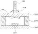
도 1 내지 도 3은 본 발명의 일 실시예에 따른 광 모듈을 설명하기 위한 분리 사시도, 결합 사시도 및 결합 단면도이다.
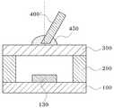
도 4는 본 발명의 일 실시예에 적용된 기판 구조의 다른 예를 나타낸 광 모듈의 결합 사시도이다.
도 5 내지 도 11은 본 발명의 일 실시예에 적용된 덮개 구조의 다양한 예들을 나타낸 단면도이다.
도 12 내지 도 14는 본 발명의 일 실시예에 적용된 광섬유의 다양한 결합구조를 설명하기 위한 단면도이다.
도 15 및 도 16은 본 발명의 일 실시예에 적용된 덮개 및 광섬유 구조의 다른 예를 설명하기 위한 단면도이다.
도 17 및 도 18은 본 발명의 일 실시예에 적용된 광소자 칩과 전자소자 칩의 결합구조를 설명하기 위한 단면도이다.
도 19는 본 발명의 일 실시예에 따른 광 모듈을 외부의 회로기판에 표면 실장하여 몰딩 처리한 구조를 설명하기 위한 단면도이다.
도 20은 본 발명의 다른 실시예에 따른 광 모듈의 구조를 설명하기 위한 단면도이다.
도 21 내지 도 27은 본 발명의 일 실시예에 따른 광 모듈의 제조방법을 설명하기 위한 사시도 및 단면도들이다.1 to 3 are an exploded perspective view, a combined perspective view, and a combined sectional view for explaining an optical module according to an embodiment of the present invention.
4 is a combined perspective view of an optical module showing another example of a substrate structure applied to an embodiment of the present invention.
5 to 11 are cross-sectional views illustrating various examples of a lid structure applied to an embodiment of the present invention.
12 to 14 are cross-sectional views illustrating various coupling structures of an optical fiber applied to an embodiment of the present invention.
15 and 16 are cross-sectional views illustrating another example of a cover and an optical fiber structure applied to an embodiment of the present invention.
17 and 18 are cross-sectional views illustrating a coupling structure of an optical device chip and an electronic device chip applied to an embodiment of the present invention.
FIG. 19 is a cross-sectional view illustrating a structure in which an optical module according to an embodiment is molded by surface-mounting an external circuit board.
20 is a cross-sectional view illustrating a structure of an optical module according to another embodiment of the present invention.
21 to 27 are perspective views and cross-sectional views illustrating a method of manufacturing an optical module according to an embodiment of the present invention.
이하, 첨부 도면을 참조하여 본 발명의 실시예를 상세하게 설명한다. 그러나, 다음에 예시하는 본 발명의 실시예는 여러 가지 다른 형태로 변형될 수 있으며, 본 발명의 범위가 다음에 상술하는 실시예에 한정되는 것은 아니다. 본 발명의 실시예는 당업계에서 통상의 지식을 가진 자에게 본 발명을 보다 완전하게 설명하기 위하여 제공되어지는 것이다.
Hereinafter, embodiments of the present invention will be described in detail with reference to the accompanying drawings. However, embodiments of the present invention illustrated below may be modified in many different forms, and the scope of the present invention is not limited to the embodiments described below. The embodiments of the present invention are provided to more completely explain the present invention to those skilled in the art.
도 1 내지 도 3은 본 발명의 일 실시예에 따른 광 모듈을 설명하기 위한 분리 사시도, 결합 사시도 및 결합 단면도이고, 도 4는 본 발명의 일 실시예에 적용된 기판 구조의 다른 예를 나타낸 광 모듈의 결합 사시도이다.1 to 3 are an exploded perspective view, a combined perspective view, and a combined sectional view for explaining an optical module according to an embodiment of the present invention, and FIG. 4 is an optical module showing another example of a substrate structure applied to an embodiment of the present invention. Is a combined perspective view.
도 1 내지 도 4를 참조하면, 본 발명의 일 실시예에 따른 광 모듈은 크게, 기판(100), 스페이서(Spacer)(200), 덮개(300) 및 광섬유(400)를 포함하여 이루어진다.1 to 4, an optical module according to an embodiment of the present invention includes a
여기서, 기판(100)은 예컨대, 사각판 형상으로 그 상부에 광소자 칩(130)이 구비되어 있으며, 스페이서(200)와 덮개(300)를 고정시키는 기반이 된다. 이러한 기판(100)의 재질로는 예컨대, 반도체(Semiconductor), 인쇄회로기판(Printed Circuit Board, PCB), 세라믹(Ceramic), 유리(Glass) 또는 플라스틱(Plastic) 등을 사용할 수 있다.Here, the
또한, 기판(100) 상에는 광소자 칩(130) 또는 광소자 칩(130)과 전자소자 칩(150, 도 17 및 도 18 참조)을 연결할 수 있도록 예컨대, 다이 본딩(Die Bonding) 및 와이어 본딩(Wire Bonding) 등을 할 수 있는 복수의 전극(111)으로 이루어진 전극패턴(110)이 형성될 수 있다. 이러한 전극패턴(110)은 외부의 회로와 전기적인 접속을 용이하게 할 수 있도록 기판(100)의 일측면으로 연장되어 형성됨이 바람직하다.Further, for example, die bonding and wire bonding (ie, die bonding and wire bonding) may be connected to the
또한, 도 4에 도시된 바와 같이, 기판(100)은 스페이서(200)보다 약간 크게 하여 다른 회로와 연결시키기 위한 전극(111)들을 스페이서(200)의 외측으로 노출시킬 수도 있고, 비아홀(Via Hole)을 사용하여 웨이퍼 레벨(Wafer Level)로 패터닝을 하고 상기 비아홀을 중심으로 다이싱(Dicing)하여 내부의 전극(111)이 자연스럽게 연결될 수 있도록 할 수도 있다.In addition, as shown in FIG. 4, the
한편, 두 개의 전극(111)만을 필요로 하는 단순한 포토다이오드(Photo Diode, PD)나 표면 발광 레이저다이오드(Vertical Cavity Surface Emitting Laser Diode, VCSLE)와 같은 단순 레이저다이오드(Laser Diode, LD)의 경우에는 기판(100) 상에 두 개의 전극(111)으로 이루어진 전극패턴(110)만 있으면 되며, 여러 전극(111)이 필요한 TIA(Transimpedance Amplifier)가 집적된 포토다이오드 광 모듈이나, 레이저다이오드(LD)에 모니터 포토다이오드(Monitor PD)가 필요한 경우에는 필요한 수만큼의 전극(111)을 형성하면 된다.Meanwhile, in the case of a simple laser diode (LD) such as a simple photo diode (PD) or a vertical cavity surface emitting laser diode (VCSLE) that requires only two
다른 한편, 기판(100)과 스페이서(200), 스페이서(200)와 덮개(300)의 결합은 예컨대, 에폭시(Epoxy), 솔더(Solder) 또는 금속(Metal) 등을 사용하여 단단히 접착할 수 있다. 이때, 솔더나 금속을 사용할 경우, 접착하고자 하는 양 접촉면에 통상의 반도체 공정을 사용하여 필요한 모양의 금속 또는 솔더패턴(120)을 형성 또는 증착하여 접착시킬 수 있다. 이 경우 전극패턴(110)과 솔더패턴(120) 사이에는 추가의 절연층 형성이 필요하다.On the other hand, the bonding of the
스페이서(200)는 높이 조절을 위한 중간층으로서, 광소자 칩(130)과 광섬유(400)의 광 결합을 일정하게 유지하기 위한 층이다.The
이러한 스페이서(200)는 기판(100)의 평면으로부터 일정한 높이를 갖는 기둥 형태(예컨대, 사각기둥, 원통형, 육각기둥 등)로 이루어지는 바, 상면과 하면의 일정영역(바람직하게, 중앙부분)을 관통하도록 관통홀(250)이 형성되어 있으며, 이러한 관통홀(250)은 기판(100)과의 결합 시 광소자 칩(130)이 삽입되어 외부로부터 광소자 칩(130)을 보호하는 기능과 광소자 칩(130), 덮개(300) 및 광섬유(400)로 구성되는 결합 광학계의 적절한 거리 설정을 하는 기능을 수행한다.The
또한, 관통홀(250)의 크기는 광소자 칩(130)과 일정간격 이격되어 삽입될 수 있도록 광소자 칩(130)보다 크게 형성됨이 바람직하다.In addition, the size of the through
한편, 스페이서(200)의 재질은 예컨대, 금속, 유리, 플라스틱, 폴리머, 세라믹 또는 반도체 등을 사용할 수 있으며, 특히 단단하면서 기판(100)이나 덮개(300)와 가깝거나 유사한 선팽창계수를 갖는 물질을 사용하는 것이 유리하다.Meanwhile, the material of the
덮개(300)는 스페이서(200)의 관통홀(250)을 폐쇄하도록 스페이서(200) 상에 결합되며, 통상 사각판 형상을 갖는다.The
이러한 덮개(300)는 사용하고자 하는 광원의 파장에서 투명한 물질을 사용하며, 양면이 연마(Polishing)된 유리, 플라스틱 또는 반도체 기판 등이 가능하다. 예를 들어, 실리콘, InP, GaAs와 같은 반도체 기판의 경우, 가시광선 영역에서는 불투명하지만, 장파장 광통신용 파장인 약 1.3um, 1.5um 대역에서는 빛을 통과하므로 본 발명의 덮개(300)로 사용할 수 있다. 한편, 도면에 도시되진 않았지만, 덮개(300)는 연마된 양면에 무반사 코팅을 수행하여 반사 손실을 줄여서 사용하는 것이 유리하다.The
그리고, 광섬유(400)는 통상적으로 빛을 이용하여 정보를 전달하기 위한 것으로서, 덮개(300) 상에 광소자 칩(130)의 위치와 대응되도록 정렬하여 예컨대, 투명한 에폭시(450)를 통해 결합되어 있다.In addition, the
이와 같이 덮개(300)에 광섬유(400)가 고정되어 광소자 칩(130)으로 빛을 입사시키거나, 반대로 광소자 칩(130)에서 방출되는 빛을 광섬유(400)로 입사시키게 된다.As described above, the
예를 들어, 광소자 칩(130)이 수광소자인 포토다이오드(PD)인 경우에는 광섬유(400)에서 출력되는 빛이 포토다이오드(PD)에 최대한 결합(Coupling)되도록 정렬을 하며, 광소자 칩(130)이 레이저다이오드(LD)나 발광다이오드(LED)와 같은 발광소자일 경우에는 광소자 칩(130)에서 방출되는 빛이 광섬유(400)로 최대한 결합되도록 광섬유(400)를 정렬하여 투명한 에폭시(450)로 고정시킨다.For example, when the
이때, 광섬유(400)의 정렬은 능동정렬(Active Alignment) 또는 수동정렬(Passive Alignment) 방법을 모두 사용할 수 있다. 상기 수동정렬의 경우에는 기판(100)에 부착된 광소자 칩(130)과의 정밀한 정렬을 위하여 필요한 패턴들이 기판(100)과 덮개(300)에 형성되어야 한다.At this time, the alignment of the
상기 능동정렬의 경우에는 기판(100)에 고정된 광소자 칩(130)으로부터 방출된 광원의 빛이 실제 광섬유(400)로 결합되거나, 또는 광섬유(400)에서 출력되는 빛이 포토다이오드(PD)에 최대한 결합되는 위치를 찾아서 투명한 에폭시(450)로 경화하여 고정시키면 된다.In the case of the active alignment, the light of the light source emitted from the
상기와 같이 구성된 본 발명의 일 실시예에 따른 광 모듈은, 광소자 칩(130)이 부착된 기판(100), 스페이서(200) 및 덮개(300)를 차례로 적체한 후, 광소자 칩(130)의 위치와 대응되도록 광섬유(400)를 정렬하여 사용하고자 하는 파장에서(또는 투과시키고자 하는 파장에서) 투명한 에폭시(450)를 이용하여 덮개(300) 상에 고정하면 완성된다.In the optical module according to the exemplary embodiment of the present invention configured as described above, the
한편, 본 발명의 일 실시예에 따른 광 모듈은 기판(100), 스페이서(200), 덮개(300) 및 광섬유(400)를 결합하여 구성하였지만, 이에 국한하지 않으며, 광섬유(400)를 부착하지 않고 PLC(Planar Lightwave Circuits)기판의 출력이나 입력 도파로(Waveguide)에 바로 붙여서 사용할 수도 있다.On the other hand, the optical module according to an embodiment of the present invention is configured by combining the
다른 한편, 광소자 칩(130)과 광섬유(400)의 광 결합 효율은, 덮개(300)의 형상 및 두께, 스페이서(200)의 두께 및 구조물 내에서의 광소자 칩(130)의 위치에 의하여 결정될 수 있다.
On the other hand, the optical coupling efficiency of the
도 5 내지 도 11은 본 발명의 일 실시예에 적용된 덮개 구조의 다양한 예들을 나타낸 단면도이다.5 to 11 are cross-sectional views illustrating various examples of a lid structure applied to an embodiment of the present invention.
도 5 내지 도 11을 참조하면, 포토다이오드(PD)로 이루어진 광소자 칩(130)의 수광 면적이 충분히 클 경우에는, 도 1 내지 도 4에 도시된 바와 같이, 양면이 편평한 덮개(300)를 사용하고, 단면이 수직 절단된 광섬유(400)를 바로 부착하여 사용할 수 있다. 또한, 덮개(300)에는 필요에 따라 덮개(300)의 양면에 무반사 광학 코팅(Anti-Reflection Optical Coating)을 형성하여 사용할 수도 있다.5 to 11, when the light receiving area of the
한편, 좀더 많은 광량을 포토다이오드(PD)에 결합시키거나, 표면 발광 레이저다이오드(VCSEL)와 발광다이오드(LED)와 같은 표면 방출형 광원 빛의 광섬유 결합효율을 향상시키기 위하여, 덮개(300)에는 렌즈(310a 및 310b)를 형성하여 사용할 수 있다.On the other hand, in order to couple more light to the photodiode PD, or to improve the optical fiber coupling efficiency of the surface-emitting light source light, such as the surface-emitting laser diode (VCSEL) and the light emitting diode (LED), the
즉, 도 5에 도시된 바와 같이, 덮개(300)의 하면(광섬유가 부착되는 면의 반대면)에 렌즈(310a)를 형성할 수 있고, 도 6에 도시된 바와 같이, 덮개(300)의 상면(광섬유가 부착되는 면)에 렌즈(310b)를 형성할 수도 있으며, 도 7에 도시된 바와 같이, 덮개(300)의 상면 및 하면에 렌즈(310a 및 310b)를 형성할 수도 있다.That is, as shown in FIG. 5, the
이때, 덮개(300)의 상면에 렌즈(310b)가 형성될 경우, 렌즈(310b)와 광섬유(400)간에 일정간격 이격되도록 투명한 에폭시(450)를 통해 고정 결합됨이 바람직하다.At this time, when the
이와 같은 렌즈(310a 및 310b)는 반도체 공정의 식각 공정을 사용하여 쉽게 제작할 수 있다. 이 때에도 필요에 따라 덮개(300)의 상면 및 하면에 무반사 광학코팅을 형성하여 사용할 수 있음은 물론이다.
또한, 도 8 내지 도 11에 도시된 바와 같이, 덮개(300) 부분의 형상을 변경하여 광섬유(400)로 되반사되는 빛의 양을 효과적으로 줄일 수 있다.In addition, as illustrated in FIGS. 8 to 11, the shape of the
즉, 도 8은 덮개(300)의 하면에 요홈 형태의 경사면(320)을 형성한 일 실시예로서, 이와 같은 구조의 덮개(300)를 사용하면 광섬유(400)의 광축에 수직으로 절단면을 형성한 광섬유(400)를 사용하면서도, 광소자 칩(130)에서 되반사되어 오는 빛이 광섬유(400)로 재입사되는 것을 효과적으로 차단할 수 있다.That is, FIG. 8 is an embodiment in which the
이때, 반사광을 효과적으로 차단할 수 있는 경사면(320)의 각도(θ')는, 광소자 칩(130)과 덮개(300)사이의 거리, 덮개(300)의 굴절율, 원하는 편광 의존성, 원하는 반사광 차단 정도에 따라 달라지며, 통상 덮개(300)의 굴절율이 약 1.5정도인 유리재질일 경우 경사면(320)의 각도(θ')는 약 6도에서 10도 정도가 사용되며, 굴절율이 약 3.4 정도인 실리콘 반도체일 경우 경사면(320)의 각도(θ')는 약 2도에서 4도 정도면 충분하다.At this time, the angle θ 'of the
또한, 도 10에 도시된 바와 같이, 경사면(320)이 형성된 상태에서 덮개(300)의 상면(광섬유가 부착되는 면)에 도 6과 같은 렌즈(310b)를 형성하여 광섬유(400)로 입사된 빛이 광소자 칩(130)에 결합되는 효율이나, 반대로 광소자 칩(130)에서 발광되는 빛이 광섬유(400)로 결합되는 효율을 향상시키도록 할 수도 있다.In addition, as shown in FIG. 10, in the state where the
이와 같은 덮개(300)의 형상은 반도체 공정에서 사용되는 여러 공정을 사용하여 제작할 수 있는데, 유리재질의 경우 정밀 금형을 사용하여 제조할 수도 있으며, 실리콘의 경우에는 방향성 식각(etching) 공정과 건식 식각(dry etching) 공정을 사용하여 형성할 수 있다.The
도 9는 도 8과 달리 덮개(300)의 하면에 돌출된 경사면(330)을 형성한 구조이며, 도 8과 동일한 효과를 가진다. 또한, 도 11에 도시된 바와 같이, 돌출된 경사면(330)이 형성된 상태에서 덮개(300)의 상면(광섬유가 부착되는 면)에 도 6과 같은 렌즈(310b)를 형성하여 광섬유(400)로 입사된 빛이 광소자 칩(130)에 결합되는 효율이나, 반대로 광소자 칩(130)에서 발광되는 빛이 광섬유(400)로 결합되는 효율을 향상시키도록 할 수도 있다.9 is a structure in which the
또한, 덮개(300)의 상면과 하면에는 원하는 광학 코팅을 증착하여 사용할 수 있음은 물론이다. 이와 같은 구조에서 경사면(320 및 330)은 덮개(300)의 상면에 형성할 수도 있으며, 이 경우에는 도 5에 도시된 바와 같이, 렌즈(310a)를 덮개(300)의 하면에 형성하는 것이 바람직하다.
In addition, the upper and lower surfaces of the
도 12 내지 도 14는 본 발명의 일 실시예에 적용된 광섬유의 다양한 결합구조를 설명하기 위한 단면도이다.12 to 14 are cross-sectional views illustrating various coupling structures of an optical fiber applied to an embodiment of the present invention.
도 12 내지 도 14를 참조하면, 통상 광섬유(400)에서 광소자 칩(130)으로 빛을 입사시키거나, 광소자 칩(130)에서 방출되는 빛을 광섬유(400)로 입사시키기 위해서는 광소자 칩(130)의 수광 혹은 발광면과 광섬유(400)가 일직선으로 정렬되는 것이 유리하나, 종종 광 모듈에서는 광섬유(400)를 통과하여 광소자 칩(130)에 입사된 빛이 되반사되어 다시 광섬유(400)로 다시 입사되는 것을 최대한 줄여야 한다.12 to 14, in order to inject light from the
이와 같은 광 모듈에서는, 광섬유(400)를 통과하여 광소자 칩(130)에 입사된 빛이 광섬유(400)로 되반사되는 것(일명, "Return Loss" 또는 "Back Reflection"라 함)을 줄이기 위하여, 도 12에 도시된 바와 같이, 광섬유(400)를 덮개(300)에 수직으로 부착하지 않고 일정각도로 기울여서 부착함으로써, 광섬유(400)로 되반사되는 빛의 양을 효과적으로 줄일 수 있다.In such an optical module, light incident through the
이때, 광섬유(400)의 기울임 각도(θ)는 약 6∼8도가 바람직하며, 포토다이오드(PD)의 경우에는 수광 면적에 따라 결합 효율이 달라진다. 수광 면적이 충분히 넓은 InGaAs 포토다이오드(PD)의 경우에는, 덮개(300)를 양면에 무반사 광학 코팅된 실리콘을 사용할 경우 약 20도 정도로 단일모드 광섬유(400)를 기울여 부착하여도 약 85%이상의 입사광 결합 효율을 확보할 수 있다.At this time, the inclination angle θ of the
이와 같은 광 모듈에서는 도 12에 도시된 바와 같이, 광섬유(400)의 단면이 광섬유(400)의 광축에 수직 절단된 광섬유(400)를 사용할 수도 있고, 도 13에 도시된 바와 같이, 광섬유(400)의 단면이 광섬유(400)의 광축에 경사면으로 절단된(Tilt Cut) 광섬유(400')를 부착하여 사용할 수도 있다.In such an optical module, as shown in FIG. 12, an
한편, 본 발명의 일 실시예에 따른 광 모듈을 활용하면, 파장다중(Wavelength Division Multiplexing, WDM) 광통신에서 필요한 파장 선택형 포토다이오드 광 모듈을 쉽게 만들 수 있다.On the other hand, by utilizing the optical module according to an embodiment of the present invention, it is possible to easily create a wavelength selective photodiode optical module required for wavelength division multiplexing (WDM) optical communication.
즉, 광섬유(400)를 통하여 전달되는 여러 파장의 빛 중에서 특정한 파장의 빛만을 통과시켜 포토다이오드(PD)에 입사시켜 검출하는 파장 선택형 포토다이오드 광 모듈을 제작하기 위하여, 도 14에 도시된 바와 같이, 덮개(300)의 한 면 또는 양면에 다층박막의 파장 선택형 필터(또는 밴드패스 필터)(320)를 코팅하여 특정한 파장의 빛만을 통과시켜 검출하게 된다.That is, in order to fabricate the wavelength selective photodiode optical module that detects the light having a specific wavelength and passes through the
이때, 덮개(300)의 한 측면에만 파장 선택형 필터(320)를 코팅하면, 다른 측면에는 무반사 광학 코팅(330)을 형성하여 사용하는 것이 유리함은 물론이다.
At this time, if the wavelength
도 15 및 도 16은 본 발명의 일 실시예에 적용된 덮개 및 광섬유 구조의 다른 예를 설명하기 위한 단면도이다.15 and 16 are cross-sectional views illustrating another example of a cover and an optical fiber structure applied to an embodiment of the present invention.
도 15 및 도 16을 참조하면, 본 발명의 일 실시예에 적용된 덮개(300) 및 광섬유(400)의 구조를 변경하여 탭 커플러 포토다이오드(Tap Coupler PD) 또는 빔 스플리팅(또는 파장 선택형) 포토다이오드(Beam Splitting PD) 광 모듈을 쉽게 제작할 수 있다.15 and 16, a tap coupler photodiode (Tap Coupler PD) or beam splitting (or wavelength selection type) is performed by changing the structure of the
즉, 제1 광섬유(400a)를 통해 입사된 광의 일부분을 포토다이오드(PD)인 광소자 칩(130)에 입사시켜 입력광의 크기를 모니터링(Monitoring)하고, 나머지 빛은 다른 경로에 위치한 제2 광섬유(400b)로 통과시키는 탭 커플러 포토다이오드(Tap coupler PD)를 제작하기 위하여, 도 15에 도시된 바와 같이, 덮개(300)의 상면 또는 하면에 광학 반사막(340)을 형성하여 제1 광섬유(400a)를 통해 전달된 입사광의 투과 및 반사도를 조절하여 원하는 양의 빛만 광소자 칩(130)으로 통과시키고, 나머지 빛은 다른 제2 광섬유(400b)로 되반사시킬 수 있다. 이때, 제1 및 제2 광섬유(400a 및 400b)는 V자 형태로 부착됨이 바람직하다.That is, a portion of the light incident through the first
이러한 광 모듈 구조의 제작 방법은 먼저, 제1 광섬유(400a)를 거쳐온 빛을 광소자 칩(130)에 정렬하여 원하는 결합을 이루고, 이러한 정렬 상태에서 다른 쪽의 제2 광섬유(400b)를 정렬하여 반사되는 광이 입사되도록 한 후에 투명한 에폭시(450)를 투여한 다음 미세 정렬을 실시하여 원하는 결합 값을 얻도록 하면 된다. 이때, 투명한 에폭시(450)는 열 또는 자외선(UV) 경화 등을 사용하는 것이 바람직하다.In the method of manufacturing the optical module structure, first, the light passing through the first
한편, 도 15에 도시된 바와 같이, 제1 및 제2 광섬유(400a 및 400b)로 분리하여 결합하였지만, 이에 국한하지 않으며, 도 16에 도시된 바와 같이, 먼저 광섬유를 결합하여 V자 형태의 광섬유(400")로 만들고, V자의 밑면을 연마하여 광학 반사막(340)으로 박막 코팅이 되어 있는 덮개(300)에 부착하면, 도 15와 동일한 결과를 얻을 수 있으며, 광섬유의 정렬과정이 단순화 될 수 있는 효과가 있다.On the other hand, as shown in Figure 15, but separated and coupled to the first and second optical fibers (400a and 400b), but is not limited to this, as shown in Figure 16, as shown in Figure 16, by combining the first optical fiber of the V-shape (400 ") and the bottom surface of the V-shape is attached to the
이와 같이 동일한 파장의 빛에 대하여, 광학 반사막(340)을 이용하여 투과율 및 반사율을 조절하여 도 15 및 도 16에 도시된 바와 같은 광 모듈을 제작하면, 광학 반사막(340)의 특성에 따라 제1 광섬유(400a)로 전달되는 동일한 파장의 빛에 대하여 일부분(예컨대, 1% 또는 2% 등)만을 광소자 칩(130)쪽으로 보내고, 나머지 빛은 제2 광섬유(400b)로 되반사시키는 탭 커플러 포토다이오드(Tap coupler PD) 광 모듈 또는 제1 광섬유(400a)로 전달되는 여러 개의 파장을 갖는 빛 중에서 특정한 파장의 빛을 광소자 칩(130)쪽으로 보내고, 나머지 빛은 제2 광섬유(400b)로 되반사시키는 빔 스플리팅(또는 파장 선택형) 포토다이오드(Beam Splitting PD) 광 모듈을 쉽게 제작할 수 있다.
As described above, when the optical module as illustrated in FIGS. 15 and 16 is manufactured by adjusting the transmittance and the reflectance using the optical reflecting
도 17 및 도 18은 본 발명의 일 실시예에 적용된 광소자 칩과 전자소자 칩의 결합구조를 설명하기 위한 단면도이다.17 and 18 are cross-sectional views illustrating a coupling structure of an optical device chip and an electronic device chip applied to an embodiment of the present invention.
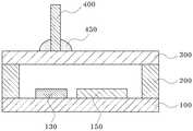
도 17 및 도 18을 참조하면, 본 발명의 일 실시예에 따른 광 모듈 구조를 활용하면 집적된(Integrated) 광소자 모듈(Module)을 쉽게 제작할 수도 있다. 즉, 광소자 칩(130)과 전자소자 칩(150)을 한 구조 안에 넣어서 광 모듈을 만드는 것도 가능하다.17 and 18, an integrated optical device module may be easily manufactured by using an optical module structure according to an embodiment of the present invention. That is, it is also possible to make an optical module by putting the
여기서, 상기 전자소자라 함은 예컨대, 인덕터, 캐패시터, 저항, 앰프(AMP), 드라이버 IC(driver IC), 컨트롤러 IC(Controller IC) 등을 말한다. 도 17에 도시된 바와 같이, 전자소자 칩(150) 상에 광소자 칩(130)이 부착될 수 있고, 도 18에 도시된 바와 같이, 광소자 칩(130)과 전자소자 칩(150)이 각기 기판(100) 상에 인접하여 부착될 수도 있다.Here, the electronic device refers to, for example, an inductor, a capacitor, a resistor, an amplifier (AMP), a driver IC, a controller IC, and the like. As shown in FIG. 17, an
전술한 바와 같이, 광소자 칩(130)과 전자소자 칩(150)이 한 구조물에 있을 경우에는, 기판(100)에 이러한 소자들 즉, 광소자 칩(130)과 전자소자 칩(150)을 부착하고 연결하여 외부로 신호를 뽑아내기 위한 전극들이 형성되어야 한다.As described above, in the case where the
이와 같은 경우에도 광섬유(400)로부터 광소자 칩(130)에 입사된 빛이 반사되어 다시 광섬유(400)로 입사되는 것을 막기 위하여, 도 12 내지 도 14에 도시된 바와 같이, 광섬유(400)를 수직축(혹은 광섬유의 광축)에 대하여 기울여 부착할 수 있음은 물론이다.
Even in such a case, in order to prevent the light incident on the
도 19는 본 발명의 일 실시예에 따른 광 모듈을 외부의 회로기판에 표면 실장하여 몰딩 처리한 구조를 설명하기 위한 단면도이다. 이러한 외부의 회로기판(500)으로는 전극의 형성이 가능한 통상의 인쇄회로기판(PCB), 세라믹, 반도체, 플라스틱, 유리 또는 폴리머 등이 사용 가능하다.FIG. 19 is a cross-sectional view illustrating a structure in which an optical module according to an embodiment is molded by surface-mounting an external circuit board. As the
도 19를 참조하면, 전술한 바와 같이 제작된 본 발명의 일 실시예에 따른 광 모듈은 외부의 회로기판(500)에 표면 실장하여 사용할 수 있다.Referring to FIG. 19, the optical module according to the embodiment of the present invention manufactured as described above may be used by surface mounting on an
즉, 본 발명의 일 실시예에 따른 광 모듈을 회로기판(500) 상에 결합하고, 리드(lid)프레임 또는 핀(pin)(550)을 연결한 후, 회로기판(500)을 포함한 기판(100), 스페이서(200), 덮개(300) 및 광섬유(400)의 일부분을 전자소자의 패키징에 많이 사용되는 EMC(Epoxy Molding Compound)(600)를 이용하여 몰딩(Molding) 처리하여 사용할 수도 있다.That is, after coupling the optical module according to an embodiment of the present invention on the
이 경우, 광섬유(400)의 외부에 별도의 보호튜브(700)를 사용하여 광섬유(400)의 과도한 구부림 발생으로 인한 광섬유(400) 손상으로부터 광섬유(400)를 효과적으로 보호할 수 있다.
In this case, a separate
도 20은 본 발명의 다른 실시예에 따른 광 모듈의 구조를 설명하기 위한 단면도이다.20 is a cross-sectional view illustrating a structure of an optical module according to another embodiment of the present invention.
도 20을 참조하면, 본 발명의 다른 실시예에 따른 광 모듈은, 전술한 본 발명의 일 실시예에 적용된 각각의 스페이서(200)와 덮개(300)를 결합하지 않고, 일체형으로 형성된 구조이다.Referring to FIG. 20, the optical module according to another embodiment of the present invention has a structure in which the
즉, 본 발명의 다른 실시예에 따른 광 모듈은, 상부에 광소자 칩(130)이 구비된 기판(100)과, 광소자 칩(130)이 전체적으로 몰딩되도록 기판(100)의 전면에 형성된 스페이서층(200')과, 스페이서층(200') 상에 광소자 칩(130)의 위치와 대응되도록 결합되는 광섬유(400)를 포함하여 이루어진다.That is, the optical module according to another embodiment of the present invention, a spacer formed on the front surface of the
이 경우 광소자 칩(130) 또는 광소자 칩(130)과 전자소자 칩(150, 도 17 및 도 18 참조)이 부착된 기판(100)에 예컨대, 투명 에폭시 또는 폴리머 수지를 부어서 몰딩 형태로 스페이서층(200')을 제작한 후, 그 위에 광섬유(400)를 부착하게 된다.In this case, for example, a transparent epoxy or polymer resin is poured onto the
이때, 광섬유(400)와 부착되는 스페이서층(200')의 표면은 투명도와 편평도를 유지하여 광이 왜곡되지 않고 광원의 빛이 광섬유(400)로 전달되거나, 광섬유(400)의 빛이 수광소자 즉, 광소자 칩(130)으로 전달될 수 있어야 한다.
At this time, the surface of the
도 21 내지 도 27은 본 발명의 일 실시예에 따른 광 모듈의 제조방법을 설명하기 위한 사시도 및 단면도들이다.21 to 27 are perspective views and cross-sectional views illustrating a method of manufacturing an optical module according to an embodiment of the present invention.
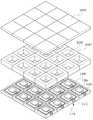
도 21 내지 도 27을 참조하면, 본 발명의 일 실시예에 따른 광 모듈의 제조방법은, 먼저 복수의 단위소자 영역으로 정의된 기판(100')을 마련한 후, 각 단위소자 영역의 기판(100') 상에 광소자 칩(130)을 각각 배열하여 결합한다.21 to 27, in the method of manufacturing an optical module according to an exemplary embodiment, a
다음으로, 복수의 관통홀(250')을 갖으며 복수의 단위소자 영역으로 정의된 스페이서층(200")을 마련한 후, 스페이서층(200")의 각 관통홀(250')에 각 광소자 칩(130)이 삽입되도록 스페이서층(200")을 기판(100') 상에 결합한다.Next, after providing a
이후에, 스페이서층(200")의 각 관통홀(250')을 폐쇄하도록 복수의 단위소자 영역으로 정의된 덮개층(300')을 결합한 후, 적어도 하나의 단위소자 영역으로 절단(Dicing)한다. 이때, 절단(Dicing)은 단위소자로 자를 수도 있고, 어레이 형태로 자를 수도 있다(도 22 및 도 23 참조).Thereafter, the cover layer 300 'defined as a plurality of unit device regions is coupled to close each through hole 250' of the
마지막으로, 상기 절단된 단위소자 영역의 덮개층(300') 상에 각 광소자 칩(130)의 위치와 대응되도록 투명한 에폭시(450)를 이용하여 광섬유(400)를 각각 배열하여 결합한다.Finally, the
한편, 광섬유(400)의 결합은 도 22에 도시된 바와 같이, 각 단위소자 영역으로 절단되기 전에 결합하여도 무방하다. 또한, 광섬유(400)는 개개의 광섬유(400)를 정렬하여 부착할 수도 있고, 어레이로 잘라진 단위소자에 대하여는 어레이 형태의 광섬유(400)를 정렬하여 붙일 수도 있다.On the other hand, the coupling of the
이와 같은 본 발명의 일 실시예에 따른 광 모듈의 제조방법에서, 기판(100')이 절연체일 경우에 바로 필요한 전극패턴(110)을 형성할 수 있으며, 기판(100')이 도체일 경우에는 먼저 유전체(dielectric)로 절연막을 형성하고, 그 위에 필요한 전극패턴(110)을 형성(증착)한 후, 다시 절연막을 형성하고, 그 위에 다시 스페이서층(200")과의 접착을 위한 솔더패턴(120)을 형성하면 된다.In the manufacturing method of the optical module according to the embodiment of the present invention, it is possible to form the required
전술한 바와 같이, 웨이퍼 레벨(Wafer Level)의 부착공정을 실시하여, 일차원적 또는 2차원적으로 절단한 후 광섬유(400)를 부착하여 제작할 수 있으며, 이때 각 광소자 칩(130) 부분마다 스페이서층(200")을 사용하지 않고, 도 25에 도시된 바와 같이, 중간 부분의 스페이서층을 생략하고, 양끝에만 스페이서층(200")을 삽입하여 광 모듈의 제작도 가능하다.As described above, the wafer level may be attached to the
한편, 도 26 및 도 27에 도시된 바와 같이, 어레이 형태의 광 모듈에 있어서, 전극(850)을 형성한 별도의 기판(800)에 전술한 도 1 내지 도 3에 도시된 바와 같은 본 발명의 기본 단위 광 모듈을 올려서 제작할 수도 있다.Meanwhile, as shown in FIGS. 26 and 27, in the optical module in the form of an array, the present invention as shown in FIGS. 1 to 3 described above on a
이러한 별도의 기판(800)으로는 전극(850)의 형성이 가능한 인쇄회로기판(PCB), 세라믹, 반도체, 플라스틱, 유리 또는 폴리머 등이 사용 가능하다. 이 경우 개개의 광 모듈의 특성을 사전에 측정하여 기판(800)에 올리게 되므로, 어레이 형태의 광 모듈의 단위 특성을 균일하게 고를 수 있으므로, 수율 면에서도 유리하다. 이와 같은 어레이 형태의 광 모듈도 도 19에 도시된 바와 같은 EMC 몰딩(Molding)을 사용하여 제작할 수 있다.
As the
전술한 본 발명에 따른 광 모듈 및 그 제조방법에 대한 바람직한 실시예에 대하여 설명하였지만, 본 발명은 이에 한정되는 것이 아니고 특허청구범위와 발명의 상세한 설명 및 첨부한 도면의 범위 안에서 여러 가지로 변형하여 실시하는 것이 가능하고 이 또한 본 발명에 속한다.
Although a preferred embodiment of the optical module according to the present invention and a method for manufacturing the same have been described, the present invention is not limited thereto, and various modifications are made within the scope of the claims and the detailed description of the invention and the accompanying drawings. It is possible to implement and this also belongs to the present invention.
Claims (22)
Translated fromKorean적어도 하나의 관통홀이 형성되며, 상기 관통홀에 상기 광소자 칩이 삽입되도록 상기 기판 상에 결합되는 스페이서;
상기 관통홀을 폐쇄하도록 상기 스페이서 상에 결합되는 덮개; 및
상기 덮개 상에 상기 광소자 칩의 위치와 대응되도록 결합되는 광섬유를 포함하며,
상기 광섬유를 통해 전달되는 빛을 상기 광소자 칩으로 입사시키거나, 상기 광소자 칩에서 방출되는 빛을 상기 광섬유로 입사시키도록 구성되며,
상기 기판의 측면으로 어레이 형태로 광소자 칩을 배열하고 외부의 회로와 전기적인 접속이 가능하도록, 상기 기판 상에는 상기 광소자 칩과 전기적으로 접속되고 상기 기판의 일측면으로 연장되는 전극패턴이 더 형성되는 것을 특징으로 하는 광 모듈.A substrate having an optical device chip thereon;
At least one through hole formed on the substrate and coupled to the substrate such that the optical device chip is inserted into the through hole;
A cover coupled to the spacer to close the through hole; And
An optical fiber coupled to the cover to correspond to a position of the optical device chip;
The light transmitted through the optical fiber is incident to the optical device chip, or the light emitted from the optical device chip is incident to the optical fiber,
An electrode pattern is further formed on the substrate to be electrically connected to the optical device chip and to extend to one side of the substrate to arrange the optical device chips in an array form on the side of the substrate and to enable electrical connection with an external circuit. Optical module characterized in that the.
상기 전극패턴에 전기적으로 접속되도록 전자소자 칩이 더 구비되되, 상기 전자소자 칩은 상기 광소자 칩의 하부 또는 주변에 구비되는 것을 특징으로 하는 광 모듈.The method according to claim 1,
An electronic device chip is further provided to be electrically connected to the electrode pattern, wherein the electronic device chip is provided below or around the optical device chip.
상기 기판의 적어도 일 측면은 상기 스페이서의 측면 외측으로 돌출 형성되는 것을 특징으로 하는 광 모듈.The method according to claim 1,
At least one side of the substrate is characterized in that the optical module protruding to the outside of the side of the spacer.
상기 광섬유는 상기 덮개 상에 투명한 에폭시를 통해 고정 결합되는 것을 특징으로 하는 광 모듈.The method according to claim 1,
And the optical fiber is fixedly coupled through the transparent epoxy on the cover.
상기 덮개의 상면 및 하면에 무반사 광학 코팅층이 더 형성되는 것을 특징으로 하는 광 모듈.The method according to claim 1,
The optical module, characterized in that the anti-reflective optical coating layer is further formed on the top and bottom of the cover.
상기 덮개의 상면 또는 하면에 상기 광섬유의 결합 위치와 대응되도록 렌즈가 더 형성되되, 상기 렌즈가 상기 덮개의 상면에 형성될 경우, 상기 렌즈와 상기 광섬유간에 일정간격 이격되도록 투명한 에폭시를 통해 고정 결합되는 것을 특징으로 하는 광 모듈.The method according to claim 1,
A lens is further formed on the upper or lower surface of the cover to correspond to the coupling position of the optical fiber, and when the lens is formed on the upper surface of the cover, the lens is fixedly fixed through a transparent epoxy so as to be spaced at a predetermined interval between the lens and the optical fiber. Optical module, characterized in that.
상기 덮개의 상면 또는 하면에 상기 광섬유의 결합 위치와 대응되도록 일정각도의 경사면을 갖는 요홈부 또는 돌출부가 더 형성되는 것을 특징으로 하는 광 모듈.The method according to claim 1,
An optical module, characterized in that the groove or protrusion having an inclined surface of a predetermined angle is further formed on the top or bottom of the cover to correspond to the coupling position of the optical fiber.
상기 요홈부 또는 돌출부가 형성되는 반대면에 상기 광섬유의 결합 위치와 대응되도록 렌즈가 더 형성되되, 상기 렌즈가 상기 덮개의 상면에 형성될 경우, 상기 렌즈와 상기 광섬유간에 일정간격 이격되도록 투명한 에폭시를 통해 고정 결합되는 것을 특징으로 하는 광 모듈.The method of claim 7, wherein
A lens is further formed to correspond to the coupling position of the optical fiber on the opposite surface on which the recess or protrusion is formed. When the lens is formed on the upper surface of the cover, a transparent epoxy is spaced apart from the lens and the optical fiber by a predetermined distance. Optical module, characterized in that fixed through.
별도의 회로기판에 상기 기판을 표면 실장하여 상기 회로기판을 포함한 기판, 스페이서, 덮개 및 광섬유의 일부분을 몰딩 처리할 경우, 상기 광섬유의 손상을 방지하기 위하여 상기 광섬유를 감싸도록 보호튜브가 더 구비되는 것을 특징으로 하는 광 모듈.The method according to claim 1,
When the substrate is mounted on a separate circuit board to mold the substrate, the spacer, the cover, and a part of the optical fiber including the circuit board, a protective tube is further provided to surround the optical fiber to prevent damage of the optical fiber. Optical module, characterized in that.
상기 광섬유를 통과하여 상기 광소자 칩에 입사된 빛이 상기 광섬유로 되반사되는 것을 방지하기 위하여 상기 광섬유의 단면이 광축에 수직 절단되거나 경사면으로 절단되어 상기 덮개 상에 일정각도로 기울어지도록 결합되는 것을 특징으로 하는 광 모듈.The method according to claim 1,
In order to prevent the light incident on the optical element chip passing through the optical fiber from being reflected back into the optical fiber, the end surface of the optical fiber is cut perpendicular to the optical axis or cut into an inclined plane and coupled to be inclined at an angle on the cover. An optical module characterized by the above-mentioned.
상기 광섬유를 통해 전달되는 여러 파장의 빛 중에서 특정파장의 빛을 통과시키도록 상기 덮개의 상면 또는 하면에 파장 선택형 필터가 더 코팅되는 것을 특징으로 하는 광 모듈.The method according to claim 1,
The optical module, characterized in that the wavelength selective filter is further coated on the upper or lower surface of the cover to pass the light of a specific wavelength among the light of various wavelengths transmitted through the optical fiber.
상기 덮개의 상면 또는 하면에 광학 반사막이 더 형성되고, 상기 광섬유를 V자 형태로 결합함으로써, 어느 한 방향의 광섬유로 전달되는 빛 중에서 특정파장의 빛을 상기 광소자 칩으로 통과시키고, 나머지 빛을 다른 한 방향의 광섬유로 되반사시키거나, 어느 한 방향의 광섬유로 전달되는 동일한 파장 빛의 일부분을 상기 광소자 칩으로 통과시키고, 나머지 빛을 다른 한 방향의 광섬유로 되반사시키는 것을 특징으로 하는 광 모듈.The method according to claim 1,
An optical reflecting film is further formed on the upper or lower surface of the cover, and by combining the optical fiber in a V shape, light of a specific wavelength is transmitted through the optical device chip among the light transmitted to the optical fiber in one direction, and the remaining light is transmitted. The light reflected by the optical fiber in one direction or a portion of the same wavelength of light transmitted to the optical fiber in one direction is passed through the optical device chip, and the other light is reflected by the optical fiber in the other direction module.
상기 광소자 칩은 상기 기판 상에 어레이 형태로 배열하여 결합되는 것을 특징으로 하는 광 모듈.The method according to claim 1,
The optical device chip is an optical module, characterized in that coupled to the array arranged on the substrate.
상기 광소자 칩이 몰딩되도록 상기 기판의 전면에 형성된 스페이서층; 및
상기 스페이서층 상에 상기 광소자 칩의 위치와 대응되도록 결합되는 광섬유를 포함하며,
상기 광섬유를 통해 전달되는 빛을 상기 광소자 칩으로 입사시키거나, 상기 광소자 칩에서 방출되는 빛을 상기 광섬유로 입사시키도록 구비되며,
상기 기판의 측면으로 어레이 형태로 광소자 칩을 배열하고 외부의 회로와 전기적인 접속이 가능하도록, 상기 기판 상에는 상기 광소자 칩과 전기적으로 접속되고 상기 기판의 일측면으로 연장되는 전극패턴이 더 형성되는 것을 특징으로 하는 광 모듈.A substrate having an optical device chip thereon;
A spacer layer formed on the front surface of the substrate to mold the optical device chip; And
An optical fiber coupled to the position of the optical device chip on the spacer layer;
Light incident through the optical fiber is incident to the optical device chip, or light emitted from the optical device chip is incident to the optical fiber,
An electrode pattern is further formed on the substrate to be electrically connected to the optical device chip and to extend to one side of the substrate to arrange the optical device chips in an array form on the side of the substrate and to enable electrical connection with an external circuit. Optical module characterized in that the.
상기 광섬유는 상기 스페이서층 상에 투명한 에폭시를 통해 고정 결합되는 것을 특징으로 하는 광 모듈.The method of claim 14,
And the optical fiber is fixedly coupled through the transparent epoxy on the spacer layer.
적어도 하나의 관통홀이 형성되며, 상기 관통홀에 상기 광소자 칩이 삽입되도록 상기 기판 상에 결합되는 스페이서; 및
상기 관통홀을 폐쇄하도록 상기 스페이서 상에 결합되는 덮개를 포함하며,
상기 기판의 측면으로 어레이 형태로 광소자 칩을 배열하고 외부의 회로와 전기적인 접속이 가능하도록, 상기 기판 상에는 상기 광소자 칩과 전기적으로 접속되고 상기 기판의 일측면으로 연장되는 전극패턴이 더 형성되는 것을 특징으로 하는 광 모듈.A substrate having an optical device chip thereon;
At least one through hole formed on the substrate and coupled to the substrate such that the optical device chip is inserted into the through hole; And
A cover coupled to the spacer to close the through hole,
An electrode pattern is further formed on the substrate to be electrically connected to the optical device chip and to extend to one side of the substrate to arrange the optical device chips in an array form on the side of the substrate and to enable electrical connection with an external circuit. Optical module characterized in that the.
적어도 하나의 관통홀을 갖는 스페이서를 마련한 후, 상기 관통홀에 상기 광소자 칩이 삽입되도록 상기 스페이서를 상기 기판 상에 결합하는 단계;
상기 관통홀을 폐쇄하도록 덮개를 결합하는 단계; 및
상기 덮개 상에 상기 광소자 칩의 위치와 대응되도록 투명한 에폭시를 이용하여 광섬유를 결합하는 단계를 포함하되,
상기 기판의 측면으로 어레이 형태로 광소자 칩을 배열하고 외부의 회로와 전기적인 접속이 가능하도록, 상기 기판 상에는 상기 광소자 칩과 전기적으로 접속되고, 상기 기판의 일측면으로 연장되는 전극패턴이 더 형성되는 것을 특징으로 하는 광 모듈의 제조방법.Coupling at least one optical device chip onto the substrate;
Providing a spacer having at least one through hole, and then coupling the spacer onto the substrate such that the optical device chip is inserted into the through hole;
Engaging a cover to close the through hole; And
Coupling an optical fiber using a transparent epoxy to correspond to the position of the optical device chip on the cover,
The electrode pattern is electrically connected to the optical device chip and extends to one side of the substrate so that the optical device chips are arranged in an array form on the side of the substrate and are electrically connected to an external circuit. Method for manufacturing an optical module, characterized in that formed.
상기 광소자 칩은 상기 기판 상에 어레이 형태로 배열하여 결합하는 것을 특징으로 하는 광 모듈의 제조방법.The method of claim 17,
The optical device chip is a manufacturing method of an optical module, characterized in that coupled to the array arranged on the substrate.
각 단위소자 영역의 기판 상에 광소자 칩을 각각 배열하여 결합하는 단계;
복수의 관통홀을 갖는 스페이서층을 마련한 후, 상기 스페이서층의 각 관통홀에 각 광소자 칩이 삽입되도록 상기 스페이서층을 상기 기판 상에 결합하는 단계;
상기 스페이서층의 각 관통홀을 폐쇄하도록 덮개층을 결합하는 단계;
적어도 하나의 단위소자 영역으로 절단하는 단계; 및
상기 절단된 단위소자 영역의 덮개층 상에 각 광소자 칩의 위치와 대응되도록 투명한 에폭시를 이용하여 광섬유를 각각 배열하여 결합하는 단계를 포함하되,
상기 기판의 측면으로 어레이 형태로 광소자 칩을 배열하고 외부의 회로와 전기적인 접속이 가능하도록, 상기 기판 상에는 상기 광소자 칩과 전기적으로 접속되고, 상기 기판의 일측면으로 연장되는 전극패턴이 형성된 광모듈의 제조 방법.Providing a substrate defined by a plurality of unit device regions;
Arranging and coupling optical device chips on a substrate in each unit device region;
After providing a spacer layer having a plurality of through holes, coupling the spacer layer onto the substrate such that each optical device chip is inserted into each through hole of the spacer layer;
Coupling a cover layer to close each through hole of the spacer layer;
Cutting into at least one unit device region; And
Arranging and coupling optical fibers using transparent epoxy so as to correspond to the position of each optical device chip on the cover layer of the cut unit device region,
An electrode pattern is formed on the substrate to be electrically connected to the optical device chip and to extend to one side of the substrate so as to arrange the optical device chips in an array form on the side of the substrate and to allow electrical connection with an external circuit. Method of manufacturing the optical module.
상기 덮개의 상면 또는 하면에 광학 반사막을 형성하는 단계를 더 포함하되,
상기 광섬유를 제1 및 제2 광섬유로 분리한 후, 상기 제1 광섬유를 통해 전달되는 빛 중에서 특정파장의 빛이나 동일한 파장 빛의 일부분을 상기 광소자 칩에 입사되도록 상기 제1 광섬유를 상기 덮개 상에 일정각도로 기울어지게 정렬하여 결합한 상태에서 상기 광학 반사막을 통해 반사되는 빛이 상기 제2 광섬유에 입사되도록 상기 제2 광섬유를 상기 덮개 상에 일정각도 기울어지게 정렬한 다음, 투명한 에폭시를 이용하여 고정 결합하는 것을 특징으로 하는 광 모듈의 제조방법.The method of claim 17 or 19,
Further comprising the step of forming an optical reflecting film on the upper or lower surface of the cover,
After the optical fiber is separated into the first and second optical fibers, the first optical fiber is formed on the cover so that a part of light of a specific wavelength or the same wavelength of light transmitted through the first optical fiber is incident on the optical device chip. The second optical fiber is aligned at an angle to the cover so that the light reflected through the optical reflecting film is incident on the second optical fiber in a state in which the light is reflected through the optical reflective film at a predetermined angle to the cover, and then fixed using a transparent epoxy. Method of manufacturing an optical module, characterized in that for coupling.
상기 덮개의 상면 또는 하면에 광학 반사막을 형성하는 단계를 더 포함하되,
상기 광섬유를 V자 형태로 제작하여 상기 광섬유의 밑면을 평평하게 연마한 후, 상기 광섬유의 연마된 밑면을 상기 덮개 상에 투명한 에폭시를 이용하여 고정 결합함으로써, 어느 한 방향으로 기울어진 광섬유를 통해 전달되는 빛 중에서 특정파장의 빛이나 동일한 파장 빛의 일부분을 상기 광소자 칩에 입사시킴과 아울러 상기 광학 반사막을 통해 반사되는 빛을 다른 한 방향으로 기울어진 광섬유에 입사시키는 것을 특징으로 하는 광 모듈의 제조방법.The method of claim 17 or 19,
Further comprising the step of forming an optical reflecting film on the upper or lower surface of the cover,
After the optical fiber is made in V shape, the bottom surface of the optical fiber is polished flat, and the polished bottom surface of the optical fiber is fixedly bonded to the cover by using a transparent epoxy, thereby transferring through the optical fiber inclined in one direction. Manufacturing a light module, characterized in that the light of a specific wavelength or a portion of the same wavelength of the light to be incident on the optical element chip, and the light reflected through the optical reflecting film is incident on the optical fiber inclined in another direction Way.
상기 광소자 칩이 몰딩되도록 상기 기판의 전면에 투명한 에폭시를 사용하여 스페이서층을 형성하는 단계; 및
상기 스페이서층 상에 상기 광소자 칩의 위치와 대응되도록 투명한 에폭시를 이용하여 광섬유를 결합하는 단계를 포함하되,
상기 기판의 측면으로 어레이 형태로 광소자 칩을 배열하고 외부의 회로와 전기적인 접속이 가능하도록, 상기 기판 상에는 상기 광소자 칩과 전기적으로 접속되고, 상기 기판의 일측면으로 연장되는 전극패턴이 형성된 광 모듈의 제조방법.Coupling at least one optical device chip onto the substrate;
Forming a spacer layer using a transparent epoxy on the entire surface of the substrate to mold the optical device chip; And
Coupling an optical fiber using a transparent epoxy so as to correspond to the position of the optical device chip on the spacer layer;
An electrode pattern is formed on the substrate to be electrically connected to the optical device chip and to extend to one side of the substrate so as to arrange the optical device chips in an array form on the side of the substrate and to allow electrical connection with an external circuit. Method of manufacturing the optical module.
Priority Applications (1)
| Application Number | Priority Date | Filing Date | Title |
|---|---|---|---|
| KR1020120000554AKR101469249B1 (en) | 2012-01-03 | 2012-01-03 | Optical module and method for fabricating the same |
Applications Claiming Priority (1)
| Application Number | Priority Date | Filing Date | Title |
|---|---|---|---|
| KR1020120000554AKR101469249B1 (en) | 2012-01-03 | 2012-01-03 | Optical module and method for fabricating the same |
Related Parent Applications (1)
| Application Number | Title | Priority Date | Filing Date |
|---|---|---|---|
| KR1020090064997ADivisionKR20110007456A (en) | 2009-07-16 | 2009-07-16 | Optical module and manufacturing method |
Publications (2)
| Publication Number | Publication Date |
|---|---|
| KR20120006096Atrue KR20120006096A (en) | 2012-01-17 |
| KR101469249B1 KR101469249B1 (en) | 2014-12-09 |
Family
ID=45611900
Family Applications (1)
| Application Number | Title | Priority Date | Filing Date |
|---|---|---|---|
| KR1020120000554AActiveKR101469249B1 (en) | 2012-01-03 | 2012-01-03 | Optical module and method for fabricating the same |
Country Status (1)
| Country | Link |
|---|---|
| KR (1) | KR101469249B1 (en) |
Cited By (2)
| Publication number | Priority date | Publication date | Assignee | Title |
|---|---|---|---|---|
| WO2017090858A1 (en)* | 2015-11-25 | 2017-06-01 | 주식회사 옵텔라 | Optical module and optical engine comprising same |
| CN111638579A (en)* | 2020-06-18 | 2020-09-08 | 刘向宁 | Optical fiber base |
Family Cites Families (4)
| Publication number | Priority date | Publication date | Assignee | Title |
|---|---|---|---|---|
| JPH10186186A (en)* | 1996-12-20 | 1998-07-14 | Oki Electric Ind Co Ltd | Optical array module |
| JP2006053360A (en)* | 2004-08-12 | 2006-02-23 | Citizen Electronics Co Ltd | Optical fiber transmitter |
| EP3540794B1 (en)* | 2006-03-10 | 2022-03-30 | Nichia Corporation | Light-emitting device |
| JP2007305736A (en)* | 2006-05-10 | 2007-11-22 | Seiko Epson Corp | Manufacturing method of optical module |
- 2012
- 2012-01-03KRKR1020120000554Apatent/KR101469249B1/enactiveActive
Cited By (2)
| Publication number | Priority date | Publication date | Assignee | Title |
|---|---|---|---|---|
| WO2017090858A1 (en)* | 2015-11-25 | 2017-06-01 | 주식회사 옵텔라 | Optical module and optical engine comprising same |
| CN111638579A (en)* | 2020-06-18 | 2020-09-08 | 刘向宁 | Optical fiber base |
Also Published As
| Publication number | Publication date |
|---|---|
| KR101469249B1 (en) | 2014-12-09 |
Similar Documents
| Publication | Publication Date | Title |
|---|---|---|
| KR20110007456A (en) | Optical module and manufacturing method | |
| US7773836B2 (en) | Integrated transceiver with lightpipe coupler | |
| KR101144665B1 (en) | Wavelengh Division Multiplexer and Demultiplexer | |
| US7476037B2 (en) | Apparatus for coupling a fiber optic cable to an optoelectronic device, a system including the apparatus, and a method of forming the same | |
| CN101458370B (en) | Optical module | |
| US7539367B2 (en) | Optical system connection structure, optical component, and optical communication module | |
| US7153037B2 (en) | Multichannel optical communications module | |
| US9581772B2 (en) | Optical electrical module used for optical communication | |
| US9020352B2 (en) | Optical communication module | |
| CN111051940A (en) | Optical interconnect module with polymer waveguides on silicon substrate | |
| US9739962B2 (en) | Plastic optical fiber data communication links | |
| US20120241600A1 (en) | Optical electrical module | |
| US20070133928A1 (en) | Canted-fiber duplex optical assembly | |
| JP2001100062A (en) | Optical communication device | |
| KR100630804B1 (en) | Multiwavelength Optical Transceiver Module, Multiplex and Demultiplexer Using Thin Film Filter | |
| US20120213527A1 (en) | Optoelectronic device for bidirectionally transporting information through optical fibers and method of manufacturing such a device | |
| US20040126118A1 (en) | Optical module and a method of fabricating the same | |
| US20050084217A1 (en) | Optical module capable of transmitting optical signal in bi-directional with single fiber | |
| US7020366B2 (en) | Light emitting device, optical module, and grating chip | |
| KR101469249B1 (en) | Optical module and method for fabricating the same | |
| US9151918B2 (en) | Opto-electronic assembly for parallel high speed transmission | |
| KR101256814B1 (en) | All passive aligned optical module and manufacturing method thereof | |
| KR100871017B1 (en) | Bi-directional triplexer optical module package with one beam splitter / filter and manufacturing method of the beam splitter / filter | |
| KR101824668B1 (en) | Optical receiver module using optical waveguide chip and method for manufacturing the same | |
| KR101175300B1 (en) | Optical module and method for fabricating the same |
Legal Events
| Date | Code | Title | Description |
|---|---|---|---|
| A107 | Divisional application of patent | ||
| PA0107 | Divisional application | Comment text:Divisional Application of Patent Patent event date:20120103 Patent event code:PA01071R01D Filing date:20090716 Application number text:1020090064997 | |
| PG1501 | Laying open of application | ||
| A201 | Request for examination | ||
| PA0201 | Request for examination | Patent event code:PA02012R01D Patent event date:20140218 Comment text:Request for Examination of Application Patent event code:PA02011R04I Patent event date:20120103 Comment text:Divisional Application of Patent | |
| E902 | Notification of reason for refusal | ||
| PE0902 | Notice of grounds for rejection | Comment text:Notification of reason for refusal Patent event date:20140519 Patent event code:PE09021S01D | |
| E701 | Decision to grant or registration of patent right | ||
| PE0701 | Decision of registration | Patent event code:PE07011S01D Comment text:Decision to Grant Registration Patent event date:20141120 | |
| PR0701 | Registration of establishment | Comment text:Registration of Establishment Patent event date:20141128 Patent event code:PR07011E01D | |
| PR1002 | Payment of registration fee | Payment date:20141201 End annual number:3 Start annual number:1 | |
| PG1601 | Publication of registration | ||
| FPAY | Annual fee payment | Payment date:20171128 Year of fee payment:4 | |
| PR1001 | Payment of annual fee | Payment date:20171128 Start annual number:4 End annual number:4 | |
| FPAY | Annual fee payment | Payment date:20181128 Year of fee payment:5 | |
| PR1001 | Payment of annual fee | Payment date:20181128 Start annual number:5 End annual number:5 | |
| FPAY | Annual fee payment | Payment date:20191126 Year of fee payment:6 | |
| PR1001 | Payment of annual fee | Payment date:20191126 Start annual number:6 End annual number:6 | |
| PR1001 | Payment of annual fee | Payment date:20201130 Start annual number:7 End annual number:7 | |
| PR1001 | Payment of annual fee | Payment date:20211129 Start annual number:8 End annual number:8 | |
| PR1001 | Payment of annual fee | Payment date:20221128 Start annual number:9 End annual number:9 | |
| PR1001 | Payment of annual fee | Payment date:20231127 Start annual number:10 End annual number:10 | |
| PR1001 | Payment of annual fee | Payment date:20241128 Start annual number:11 End annual number:11 |