KR20120000748A - Semiconductor device and manufacturing method thereof - Google Patents
Semiconductor device and manufacturing method thereofDownload PDFInfo
- Publication number
- KR20120000748A KR20120000748AKR1020100061184AKR20100061184AKR20120000748AKR 20120000748 AKR20120000748 AKR 20120000748AKR 1020100061184 AKR1020100061184 AKR 1020100061184AKR 20100061184 AKR20100061184 AKR 20100061184AKR 20120000748 AKR20120000748 AKR 20120000748A
- Authority
- KR
- South Korea
- Prior art keywords
- silicon
- insulating film
- via contact
- insulating layer
- forming
- Prior art date
- Legal status (The legal status is an assumption and is not a legal conclusion. Google has not performed a legal analysis and makes no representation as to the accuracy of the status listed.)
- Withdrawn
Links
Images


Classifications
- H—ELECTRICITY
- H01—ELECTRIC ELEMENTS
- H01L—SEMICONDUCTOR DEVICES NOT COVERED BY CLASS H10
- H01L21/00—Processes or apparatus adapted for the manufacture or treatment of semiconductor or solid state devices or of parts thereof
- H01L21/70—Manufacture or treatment of devices consisting of a plurality of solid state components formed in or on a common substrate or of parts thereof; Manufacture of integrated circuit devices or of parts thereof
- H01L21/71—Manufacture of specific parts of devices defined in group H01L21/70
- H01L21/768—Applying interconnections to be used for carrying current between separate components within a device comprising conductors and dielectrics
- H01L21/76898—Applying interconnections to be used for carrying current between separate components within a device comprising conductors and dielectrics formed through a semiconductor substrate
- H—ELECTRICITY
- H01—ELECTRIC ELEMENTS
- H01L—SEMICONDUCTOR DEVICES NOT COVERED BY CLASS H10
- H01L21/00—Processes or apparatus adapted for the manufacture or treatment of semiconductor or solid state devices or of parts thereof
- H01L21/70—Manufacture or treatment of devices consisting of a plurality of solid state components formed in or on a common substrate or of parts thereof; Manufacture of integrated circuit devices or of parts thereof
- H01L21/71—Manufacture of specific parts of devices defined in group H01L21/70
- H01L21/768—Applying interconnections to be used for carrying current between separate components within a device comprising conductors and dielectrics
- H01L21/76801—Applying interconnections to be used for carrying current between separate components within a device comprising conductors and dielectrics characterised by the formation and the after-treatment of the dielectrics, e.g. smoothing
- H—ELECTRICITY
- H01—ELECTRIC ELEMENTS
- H01L—SEMICONDUCTOR DEVICES NOT COVERED BY CLASS H10
- H01L25/00—Assemblies consisting of a plurality of semiconductor or other solid state devices
- H01L25/03—Assemblies consisting of a plurality of semiconductor or other solid state devices all the devices being of a type provided for in a single subclass of subclasses H10B, H10D, H10F, H10H, H10K or H10N, e.g. assemblies of rectifier diodes
- H01L25/04—Assemblies consisting of a plurality of semiconductor or other solid state devices all the devices being of a type provided for in a single subclass of subclasses H10B, H10D, H10F, H10H, H10K or H10N, e.g. assemblies of rectifier diodes the devices not having separate containers
- H01L25/065—Assemblies consisting of a plurality of semiconductor or other solid state devices all the devices being of a type provided for in a single subclass of subclasses H10B, H10D, H10F, H10H, H10K or H10N, e.g. assemblies of rectifier diodes the devices not having separate containers the devices being of a type provided for in group H10D89/00
- H01L25/0657—Stacked arrangements of devices
- H—ELECTRICITY
- H01—ELECTRIC ELEMENTS
- H01L—SEMICONDUCTOR DEVICES NOT COVERED BY CLASS H10
- H01L21/00—Processes or apparatus adapted for the manufacture or treatment of semiconductor or solid state devices or of parts thereof
- H01L21/70—Manufacture or treatment of devices consisting of a plurality of solid state components formed in or on a common substrate or of parts thereof; Manufacture of integrated circuit devices or of parts thereof
- H01L21/71—Manufacture of specific parts of devices defined in group H01L21/70
- H01L21/768—Applying interconnections to be used for carrying current between separate components within a device comprising conductors and dielectrics
- H01L21/76801—Applying interconnections to be used for carrying current between separate components within a device comprising conductors and dielectrics characterised by the formation and the after-treatment of the dielectrics, e.g. smoothing
- H01L21/76802—Applying interconnections to be used for carrying current between separate components within a device comprising conductors and dielectrics characterised by the formation and the after-treatment of the dielectrics, e.g. smoothing by forming openings in dielectrics
- H01L21/76804—Applying interconnections to be used for carrying current between separate components within a device comprising conductors and dielectrics characterised by the formation and the after-treatment of the dielectrics, e.g. smoothing by forming openings in dielectrics by forming tapered via holes
- H—ELECTRICITY
- H01—ELECTRIC ELEMENTS
- H01L—SEMICONDUCTOR DEVICES NOT COVERED BY CLASS H10
- H01L2224/00—Indexing scheme for arrangements for connecting or disconnecting semiconductor or solid-state bodies and methods related thereto as covered by H01L24/00
- H01L2224/01—Means for bonding being attached to, or being formed on, the surface to be connected, e.g. chip-to-package, die-attach, "first-level" interconnects; Manufacturing methods related thereto
- H01L2224/10—Bump connectors; Manufacturing methods related thereto
- H01L2224/15—Structure, shape, material or disposition of the bump connectors after the connecting process
- H01L2224/16—Structure, shape, material or disposition of the bump connectors after the connecting process of an individual bump connector
- H—ELECTRICITY
- H01—ELECTRIC ELEMENTS
- H01L—SEMICONDUCTOR DEVICES NOT COVERED BY CLASS H10
- H01L2225/00—Details relating to assemblies covered by the group H01L25/00 but not provided for in its subgroups
- H01L2225/03—All the devices being of a type provided for in the same main group of the same subclass of class H10, e.g. assemblies of rectifier diodes
- H01L2225/04—All the devices being of a type provided for in the same main group of the same subclass of class H10, e.g. assemblies of rectifier diodes the devices not having separate containers
- H01L2225/065—All the devices being of a type provided for in the same main group of the same subclass of class H10
- H01L2225/06503—Stacked arrangements of devices
- H01L2225/06513—Bump or bump-like direct electrical connections between devices, e.g. flip-chip connection, solder bumps
- H—ELECTRICITY
- H01—ELECTRIC ELEMENTS
- H01L—SEMICONDUCTOR DEVICES NOT COVERED BY CLASS H10
- H01L2225/00—Details relating to assemblies covered by the group H01L25/00 but not provided for in its subgroups
- H01L2225/03—All the devices being of a type provided for in the same main group of the same subclass of class H10, e.g. assemblies of rectifier diodes
- H01L2225/04—All the devices being of a type provided for in the same main group of the same subclass of class H10, e.g. assemblies of rectifier diodes the devices not having separate containers
- H01L2225/065—All the devices being of a type provided for in the same main group of the same subclass of class H10
- H01L2225/06503—Stacked arrangements of devices
- H01L2225/06541—Conductive via connections through the device, e.g. vertical interconnects, through silicon via [TSV]
- H—ELECTRICITY
- H01—ELECTRIC ELEMENTS
- H01L—SEMICONDUCTOR DEVICES NOT COVERED BY CLASS H10
- H01L25/00—Assemblies consisting of a plurality of semiconductor or other solid state devices
- H01L25/18—Assemblies consisting of a plurality of semiconductor or other solid state devices the devices being of the types provided for in two or more different main groups of the same subclass of H10B, H10D, H10F, H10H, H10K or H10N
Landscapes
- Engineering & Computer Science (AREA)
- Microelectronics & Electronic Packaging (AREA)
- Power Engineering (AREA)
- Physics & Mathematics (AREA)
- Condensed Matter Physics & Semiconductors (AREA)
- General Physics & Mathematics (AREA)
- Computer Hardware Design (AREA)
- Manufacturing & Machinery (AREA)
- Internal Circuitry In Semiconductor Integrated Circuit Devices (AREA)
Abstract
Translated fromKoreanDescription
Translated fromKorean본 발명은 반도체 소자 및 그 제조 방법에 관한 것이다. 보다 상세하게는, 실리콘 관통 비아(TSV, Through Silicon Via) 콘택을 포함하는 반도체 소자 및 그 제조 방법에 관한 것이다.The present invention relates to a semiconductor device and a method of manufacturing the same. More specifically, the present invention relates to a semiconductor device including a through silicon via (TSV) contact and a method of manufacturing the same.
반도체 소자가 고도로 집적화되고 대용량화됨에 따라, 각 개별 칩들을 적층시키는 3차원 패키지 기술이 개발되고 있다. 이 중, 실리콘 관통 비아 콘택(Through Silicon Via Contact) 기술은 기존의 와이어 본딩 기술을 대체하는 기술로써 기판을 관통하는 비아홀을 형성하고 상기 비아홀 내에 전극을 형성하는 패키지 기술이다.As semiconductor devices are highly integrated and large in capacity, three-dimensional package technology for stacking individual chips is being developed. Among these, through silicon via contact technology is a package technology that forms a via hole through a substrate and forms an electrode in the via hole as a technology to replace a conventional wire bonding technology.
최근에는 하나의 칩 당 수 천개 이상의 실리콘 관통 비아 콘택이 필요하다. 또한, 상기 실리콘 관통 비아 콘택이 낮은 저항을 가짐으로써 높은 데이터 전송이 가능하여야 한다. 이와 같이, 실리콘 관통 비아 콘택의 저항이 감소됨에 따라 상기 실리콘 관통 비아 콘택과 반도체 기판 간의 기생 커패시턴스가 증가되는 등의 문제가 발생된다. 이로 인해, 상기 실리콘 관통 비아 콘택을 포함하는 반도체 소자의 신뢰성이 저하된다.Recently, thousands of silicon through via contacts are required per chip. In addition, the silicon through via contact should have a low resistance to enable high data transmission. As such, as the resistance of the through silicon via contact decreases, a problem such as an increase in the parasitic capacitance between the through silicon via and the semiconductor substrate occurs. As a result, the reliability of the semiconductor device including the silicon through via contact is reduced.
본 발명의 목적은 기생 커패시턴스가 감소되고 높은 신뢰성을 갖는 반도체 소자를 제공하는데 있다.It is an object of the present invention to provide a semiconductor device having reduced parasitic capacitance and high reliability.
본 발명의 다른 목적은 상기한 반도체 소자의 제조 방법을 제공하는데 있다.Another object of the present invention is to provide a method for manufacturing the semiconductor device described above.
상기한 목적을 달성하기 위한 본 발명의 일 실시예에 따른 반도체 소자는, 기판 상에 회로 패턴들이 구비된다. 상기 회로 패턴들을 덮고, 상부면으로부터 상기 기판 내부까지 관통하는 관통홀을 포함하는 층간 절연막이 구비된다. 상기 관통홀의 측벽, 저면 및 층간 절연막 상부면을 따라 연속적으로 절연막 구조물이 구비된다. 상기 관통홀 내부에 구비되고, 상기 층간 절연막 상의 절연막 구조물의 상부면과 동일한 상부면 높이를 갖는 실리콘 관통 비아 콘택이 구비된다. 상기 실리콘 관통 비아 콘택 및 절연막 구조물 상부면을 덮는 버퍼막이 구비된다. 또한, 상기 버퍼막, 절연막 구조물 및 층간 절연막을 관통하여 상기 회로 패턴들과 연결되는 콘택 플러그를 포함한다.In the semiconductor device according to the embodiment of the present invention for achieving the above object, circuit patterns are provided on a substrate. An interlayer insulating layer covering the circuit patterns and including a through hole penetrating from an upper surface to an inside of the substrate is provided. An insulating film structure is continuously provided along the sidewalls, the bottom surface of the through hole, and the upper surface of the interlayer insulating film. A silicon through via contact provided in the through hole and having the same upper surface height as the upper surface of the insulating film structure on the interlayer insulating layer is provided. A buffer layer covering the silicon through via contact and the upper surface of the insulating layer structure is provided. The semiconductor device may further include contact plugs penetrating the buffer layer, the insulating layer structure, and the interlayer insulating layer to be connected to the circuit patterns.
본 발명의 일 실시예로, 상기 실리콘 관통 비아 콘택은 베리어 금속 및 구리를 포함할 수 있다.In one embodiment of the present invention, the silicon through via contact may include a barrier metal and copper.
본 발명의 일 실시예로, 상기 버퍼막은 실리콘 질화물, 실리콘 탄소 질화물, 및 SiCON으로 이루어진 군에서 선택된 적어도 하나를 포함할 수 있다.In one embodiment of the present invention, the buffer film may include at least one selected from the group consisting of silicon nitride, silicon carbon nitride, and SiCON.
본 발명의 일 실시예로, 상기 절연막 구조물은 1000Å보다 두껍고 상기 관통홀 직경의 1/4의 두께 보다는 얇은 두께를 가질 수 있다.In one embodiment of the present invention, the insulating film structure may have a thickness thicker than 1000mm and thinner than a thickness of 1/4 of the through hole diameter.
본 발명의 일 실시예로, 상기 절연막 구조물은 실리콘 산화물 또는 탄소 도핑된 실리콘 산화물을 포함할 수 있다.In one embodiment of the present invention, the insulating film structure may include silicon oxide or carbon doped silicon oxide.
본 발명의 일 실시예로, 상기 실리콘 관통 비아 콘택 및 콘택 플러그와 연결되는 상부 배선 구조물을 더 포함할 수 있다. 상기 상부 배선 구조물은 구리를 포함할 수 있다.In an embodiment, the semiconductor device may further include an upper wiring structure connected to the silicon through via contact and the contact plug. The upper wiring structure may include copper.
본 발명의 일 실시예로, 상기 콘택 플러그는 금속 물질을 포함할 수 있다.In one embodiment of the present invention, the contact plug may include a metal material.
본 발명의 일 실시예로, 상기 실리콘 관통 비아 콘택에 포함되는 도전 패턴은 상기 관통홀 내부를 채우는 원통 형상을 가질 수 있다.In an embodiment, the conductive pattern included in the through silicon via contact may have a cylindrical shape filling the inside of the through hole.
본 발명의 일 실시예로, 상기 절연막 구조물은 상기 관통홀 측벽 및 저면에 형성되는 제1 절연막 및 상기 층간 절연막 상에 형성되는 제2 절연막을 구비하고, 상기 제1 절연막과 상기 제2 절연막은 서로 다른 두께를 가질 수 있다.In an embodiment, the insulating film structure may include a first insulating film formed on the sidewalls and the bottom surface of the through hole, and a second insulating film formed on the interlayer insulating film, wherein the first insulating film and the second insulating film are mutually It may have a different thickness.
본 발명의 일 실시예로, 상기 실리콘 관통 비아 콘택은, 상기 관통홀의 측벽 및 저면을 따라 증착된 실린더 형상 도전 패턴을 포함할 수 있다. 또한, 상기 실린더 내부를 채우는 갭필 패턴을 포함할 수 있다.In one embodiment of the present invention, the silicon through via contact may include a cylindrical conductive pattern deposited along the sidewall and the bottom surface of the through hole. In addition, it may include a gap fill pattern filling the inside of the cylinder.
상기한 목적을 달성하기 위한 본 발명의 다른 실시예에 따른 반도체 소자는, 제1 기판 상에 형성된 제1 회로 패턴들을 덮고, 상부면으로부터 기판을 관통하는 관통홀을 포함하는 층간 절연막이 구비된다. 상기 관통홀의 측벽 및 층간 절연막 상부면에 절연막 구조물이 구비된다. 상기 관통홀 내부에는 상기 층간 절연막 상의 절연막 구조물의 상부면과 동일한 상부면 높이를 갖고, 하부면이 상기 기판 저면에 노출되는 실리콘 관통 비아 콘택이 구비된다. 상기 실리콘 관통 비아 콘택 및 절연막 구조물 상부면을 덮는 버퍼막이 구비된다. 상기 버퍼막, 절연막 구조물 및 층간 절연막을 관통하여 상기 제1 회로 패턴들과 연결되는 콘택 플러그가 구비된다. 상기 콘택 플러그 및 상기 실리콘 관통 비아 콘택 상부면과 전기적으로 연결되는 배선 구조물이 구비된다. 제2 회로 패턴들 및 패드 전극들이 포함되는 제2 기판이 구비된다. 상기 제2 기판의 패드 전극들과 실리콘 관통 비아 콘택의 저면을 전기적으로 접촉시키는 접촉 패턴을 포함한다.A semiconductor device according to another embodiment of the present invention for achieving the above object includes an interlayer insulating film covering a first circuit pattern formed on a first substrate and including a through hole penetrating through the substrate from an upper surface thereof. An insulating layer structure is provided on the sidewall of the through hole and the upper surface of the interlayer insulating layer. The through-hole has a silicon through via contact having the same upper surface height as the upper surface of the insulating film structure on the interlayer insulating layer, and the lower surface is exposed to the bottom surface of the substrate. A buffer layer covering the silicon through via contact and the upper surface of the insulating layer structure is provided. Contact plugs are formed to penetrate the buffer layer, the insulating layer structure, and the interlayer insulating layer to be connected to the first circuit patterns. A wiring structure electrically connected to the contact plug and the silicon through via contact upper surface is provided. A second substrate including second circuit patterns and pad electrodes is provided. And a contact pattern for electrically contacting pad electrodes of the second substrate and a bottom surface of the silicon through via contact.
본 발명의 일 실시예로, 상기 실리콘 관통 비아 콘택은 베리어 금속 및 구리를 포함할 수 있다.In one embodiment of the present invention, the silicon through via contact may include a barrier metal and copper.
본 발명의 일 실시예로, 상기 버퍼막은 실리콘 질화물, 실리콘 탄소 질화물, 및 SiCON으로 이루어진 군에서 선택된 적어도 하나를 포함할 수 있다.In one embodiment of the present invention, the buffer film may include at least one selected from the group consisting of silicon nitride, silicon carbon nitride, and SiCON.
본 발명의 일 실시예로, 상기 절연막 구조물은 실리콘 산화물 또는 탄소 도핑된 실리콘 산화물을 포함할 수 있다.In one embodiment of the present invention, the insulating film structure may include silicon oxide or carbon doped silicon oxide.
상기한 목적을 달성하기 위한 본 발명의 일 실시예에 따른 반도체 소자의 제조 방법으로, 기판 상에 회로 패턴들을 형성한다. 상기 회로 패턴들을 덮고, 상부면으로부터 기판 내부까지 관통하는 관통홀을 포함하는 층간 절연막을 형성한다. 상기 관통홀의 측벽, 저면 및 층간 절연막 상부면을 따라 연속적으로 절연막 구조물을 형성한다. 상기 관통홀 내부를 채우면서, 상기 층간 절연막 상의 절연막 구조물의 상부면과 동일한 상부면 높이를 갖는 실리콘 관통 비아 콘택을 형성한다. 상기 실리콘 관통 비아 콘택 및 절연막 구조물 상부면을 덮는 버퍼막을 형성한다. 또한, 상기 버퍼막, 절연막 구조물 및 층간 절연막을 관통하여 상기 회로 패턴들과 연결되는 콘택 플러그를 형성한다.In a method of manufacturing a semiconductor device according to an embodiment of the present invention for achieving the above object, circuit patterns are formed on a substrate. An interlayer insulating layer covering the circuit patterns and including a through hole penetrating from the upper surface to the inside of the substrate is formed. An insulating film structure is continuously formed along the sidewalls, the bottom surface of the through hole, and the upper surface of the interlayer insulating film. While filling the inside of the through hole, a silicon through via contact having a same upper surface height as an upper surface of the insulating film structure on the interlayer insulating film is formed. A buffer layer is formed to cover the silicon through via contact and the upper surface of the insulating layer structure. In addition, a contact plug is formed to penetrate the buffer layer, the insulating layer structure, and the interlayer insulating layer to be connected to the circuit patterns.
본 발명의 일 실시예로, 상기 실리콘 관통 비아 콘택을 형성하기 위하여, 상기 관통홀 내부의 절연막 구조물 상에 배리어 막을 형성한다. 상기 배리어 막 상에 상기 관통홀을 채우도록 구리막을 형성한다. 또한, 상기 절연막 구조물의 상부면이 노출되도록 상기 구리막 및 배리어 막을 연마하여 실리콘 관통 비아 콘택을 형성한다.In an embodiment, a barrier layer is formed on the insulating layer structure inside the through hole to form the silicon through via contact. A copper film is formed on the barrier film to fill the through hole. In addition, the copper layer and the barrier layer may be polished to expose the upper surface of the insulating layer structure to form a silicon through via contact.
이에 더하여, 상기 실리콘 관통 비아 콘택의 상부면이 상기 절연막 구조물보다 돌출되도록 상기 실리콘 관통 비아 콘택을 열처리한다. 또한, 상기 실리콘 관통 비아 콘택 및 절연막 구조물의 상부면이 평탄하도록 상기 돌출된 부위의 실리콘 관통 비아 콘택을 연마한다.In addition, the silicon through via contact is heat-treated such that an upper surface of the through silicon via contact protrudes from the insulating layer structure. In addition, the silicon through via contact of the protruding portion is polished such that the silicon through via contact and the top surface of the insulating layer structure are flat.
상기 열처리는 100 내지 600℃의 온도로 수행할 수 있다.The heat treatment may be performed at a temperature of 100 to 600 ℃.
상기 실리콘 관통 비아 콘택을 형성하기 위한 연마 공정을 수행할 때 상기 상부 절연막 구조물 상에 위치하는 제2 절연막의 일부가 함께 연마되고, 상기 연마 공정 이 후의 제2 절연막의 두께는 증착 시의 제2 절연막 두께의 30% 이상의 두께를 가질 수 있다.When performing the polishing process for forming the through silicon via contact, a part of the second insulating film positioned on the upper insulating film structure is polished together, and the thickness of the second insulating film after the polishing process is the second insulating film during deposition. It may have a thickness of at least 30% of the thickness.
본 발명의 일 실시예로, 상기 실리콘 관통 비아 콘택을 형성하기 위하여, 상기 관통홀 내부의 절연막 구조물 상에 배리어 막을 형성한다. 상기 배리어 막 상에 상기 관통홀 측벽 및 저면을 따라 구리막을 형성한다. 상기 구리막 상에 상기 관통홀을 채우는 갭필용 막을 형성한다. 또한, 상기 절연막 구조물의 상부면이 노출되도록 상기 구리막, 배리어 막 및 갭필용 막을 연마하여 실리콘 관통 비아 콘택을 형성한다.In an embodiment, a barrier layer is formed on the insulating layer structure inside the through hole to form the silicon through via contact. A copper film is formed on the barrier film along sidewalls and bottom surfaces of the through holes. A gap fill film is formed on the copper film to fill the through hole. In addition, the copper layer, the barrier layer, and the gap fill layer may be polished to expose the upper surface of the insulating layer structure to form a silicon through via contact.
본 발명의 일 실시예로, 상기 콘택 플러그 및 상기 실리콘 관통 비아 콘택과 전기적으로 연결되는 배선 구조물을 형성하는 공정이 더 포함될 수 있다.In an embodiment, the method may further include forming a wiring structure electrically connected to the contact plug and the silicon through via contact.
본 발명의 일 실시예로, 상기 버퍼막은 실리콘 질화물, 실리콘 탄소 질화물, SiCON으로 이루어지는 군에서 선택된 적어도 하나의 물질을 포함할 수 있다.In one embodiment of the present invention, the buffer film may include at least one material selected from the group consisting of silicon nitride, silicon carbon nitride, and SiCON.
본 발명의 일 실시예로, 상기 절연막 구조물은 1000Å보다 두껍고 상기 관통홀 직경의 1/4의 두께보다는 얇은 두께를 갖도록 형성할 수 있다.In one embodiment of the present invention, the insulating film structure may be formed to have a thickness thicker than 1000Å and thinner than a thickness of 1/4 of the through hole diameter.
본 발명의 일 실시예로, 상기 절연막 구조물은 실리콘 산화물 또는 탄소 도핑된 실리콘 산화물을 증착시켜 형성할 수 있다.In one embodiment of the present invention, the insulating film structure may be formed by depositing silicon oxide or carbon doped silicon oxide.
본 발명의 일 실시예로, 상기 콘택 플러그를 형성하기 위하여, 상기 버퍼막, 절연막 구조물 및 층간 절연막을 식각하여 콘택홀을 형성한다. 상기 콘택홀 내부에 금속막을 형성한다. 또한, 상기 버퍼막 표면이 노출되도록 상기 금속막을 연마하여 상기 콘택홀 내부에 콘택 플러그를 형성한다.In an embodiment of the present invention, in order to form the contact plug, a contact hole is formed by etching the buffer film, the insulating film structure, and the interlayer insulating film. A metal film is formed in the contact hole. In addition, the metal film is polished to expose the surface of the buffer film to form a contact plug inside the contact hole.
본 발명의 일 실시예로, 상기 절연막 구조물을 형성하는 단계에서, 관통홀의 측벽 및 저면에 형성되는 제1 절연막은 상기 층간 절연막 상에 형성되는 제2 절연막보다 더 두껍게 형성될 수 있다.In an embodiment of the present disclosure, in the forming of the insulating layer structure, the first insulating layer formed on the sidewall and the bottom surface of the through hole may be thicker than the second insulating layer formed on the interlayer insulating layer.
상기 제2 절연막 및 제1 절연막은 1 : 0.3 내지 0.8의 두께 비를 가질 수 있다.The second insulating film and the first insulating film may have a thickness ratio of 1: 0.3 to 0.8.
상기한 목적을 달성하기 위한 본 발명의 다른 실시예에 따른 반도체 소자의 제조 방법으로, 제1 기판 상에 형성된 제1 회로 패턴들을 덮고, 상부면으로부터 기판을 관통하는 관통홀을 포함하는 층간 절연막을 형성한다. 상기 관통홀의 측벽 및 층간 절연막 상부면에 절연막 구조물을 형성한다. 상기 관통홀 내부에 구비되고, 상기 층간 절연막 상의 절연막 구조물의 상부면과 동일한 상부면 높이를 갖고, 하부면이 상기 기판 저면에 노출되는 실리콘 관통 비아 콘택을 형성한다. 상기 실리콘 관통 비아 콘택 및 절연막 구조물 상부면을 덮는 버퍼막을 형성한다. 상기 버퍼막, 절연막 구조물 및 층간 절연막을 관통하여 상기 제1 회로 패턴들과 연결되는 콘택 플러그를 형성한다. 상기 콘택 플러그 및 상기 실리콘 관통 비아 콘택 상부면과 전기적으로 연결되는 배선 구조물을 형성한다. 제2 기판에 제2 회로 패턴들 및 패드 전극들을 형성한다. 또한, 상기 제2 기판의 패드 전극들과 실리콘 관통 비아 콘택의 저면을 전기적으로 접촉시키는 접촉 패턴을 형성한다.In another aspect of the present invention, there is provided a method of manufacturing a semiconductor device. Form. An insulating film structure is formed on the sidewall of the through hole and the upper surface of the interlayer insulating film. A silicon through via contact is formed in the through hole and has the same upper surface height as that of the upper surface of the insulating film structure on the interlayer insulating layer, and the lower surface is exposed to the bottom surface of the substrate. A buffer layer is formed to cover the silicon through via contact and the upper surface of the insulating layer structure. A contact plug is formed to penetrate the buffer layer, the insulating layer structure, and the interlayer insulating layer to be connected to the first circuit patterns. And a wiring structure electrically connected to the contact plug and the silicon through via contact top surface. Second circuit patterns and pad electrodes are formed on the second substrate. In addition, a contact pattern is formed to electrically contact the pad electrodes of the second substrate with the bottom surface of the silicon through via contact.
본 발명의 일 실시예로, 상기 실리콘 관통 비아 콘택은 베리어 금속 및 구리를 포함할 수 있다.In one embodiment of the present invention, the silicon through via contact may include a barrier metal and copper.
본 발명의 일 실시예로, 상기 버퍼막은 실리콘 질화물, 실리콘 탄소 질화물, SiCON으로 이루어지는 군에서 선택된 적어도 하나의 물질을 포함할 수 있다.In one embodiment of the present invention, the buffer film may include at least one material selected from the group consisting of silicon nitride, silicon carbon nitride, and SiCON.
설명한 것과 같이, 본 발명에 따른 반도체 소자는 실리콘 관통 비아 콘택과 반도체 기판 사이의 기생 커패시턴스가 감소된다. 그러므로, 상기 반도체 소자는 신호 및 데이터 전송 속도가 빠르다. 또한, 상기 실리콘 관통 비아 콘택을 형성할 때 연마에 의해 제거되는 막의 두께가 감소됨으로써, 실리콘 관통 비아 콘택의 계면 특성 및 저항 특성을 양호하게 할 수 있다. 그러므로, 우수한 특성 및 높은 신뢰성을 갖는 반도체 소자를 제공할 수 있다.As described, the semiconductor device according to the present invention reduces the parasitic capacitance between the silicon through via contact and the semiconductor substrate. Therefore, the semiconductor device has a high signal and data transfer rate. In addition, when forming the through silicon via contact, the thickness of the film removed by polishing is reduced, so that the interfacial and resistive properties of the through silicon via contact are improved. Therefore, it is possible to provide a semiconductor device having excellent characteristics and high reliability.
도 1은 본 발명의 일 실시예에 따른 반도체 소자를 단면도이다.
도 2 내지 도 10은 도 1에 도시된 반도체 소자를 제조하는 제1 방법을 나타내는 단면도들이다.
도 11 및 12는 도 1에 도시된 반도체 소자를 제조하는 제2 방법을 나타내는 단면도들이다.
도 13은 본 발명의 일 실시예에 따른 적층형 반도체 소자를 나타내는 단면도들이다.
도 14 내지 도 19는 도 10에 도시된 적층형 반도체 소자의 제조 방법을 나타내는 단면도들이다.
도 20은 본 발명의 일 실시예에 따른 반도체 소자를 단면도이다.
도 21 및 도 22는 도 20에 도시된 반도체 소자를 제조하는 방법을 나타내는 단면도들이다.
도 23은 본 발명의 일 실시예에 따른 적층형 반도체 소자를 나타내는 단면도들이다.
도 24는 본 발명의 다른 실시예를 도시한 것이다.
도 25는 또 다른 실시예를 도시한 것이다.
도 26은 또 다른 실시예를 도시한 것이다.1 is a cross-sectional view of a semiconductor device in accordance with an embodiment of the present invention.
2 to 10 are cross-sectional views illustrating a first method of manufacturing the semiconductor device illustrated in FIG. 1.
11 and 12 are cross-sectional views illustrating a second method of manufacturing the semiconductor device illustrated in FIG. 1.
13 is a cross-sectional view illustrating a stacked semiconductor device according to an exemplary embodiment of the present invention.
14 to 19 are cross-sectional views illustrating a method of manufacturing the stacked semiconductor device illustrated in FIG. 10.
20 is a cross-sectional view of a semiconductor device according to example embodiments.
21 and 22 are cross-sectional views illustrating a method of manufacturing the semiconductor device shown in FIG. 20.
23 is a cross-sectional view illustrating a stacked semiconductor device according to an embodiment of the present invention.
24 shows another embodiment of the present invention.
25 shows another embodiment.
26 shows yet another embodiment.
이하, 첨부한 도면을 참조하여 본 발명의 바람직한 실시예를 상세히 설명하고자 한다.Hereinafter, exemplary embodiments of the present invention will be described in detail with reference to the accompanying drawings.
본 발명의 각 도면에 있어서, 구조물들의 치수는 본 발명의 명확성을 기하기 위하여 실제보다 확대하여 도시한 것이다.In the drawings of the present invention, the dimensions of the structures are enlarged to illustrate the present invention in order to clarify the present invention.
본 발명에서, 제1, 제2 등의 용어는 다양한 구성요소들을 설명하는데 사용될 수 있지만, 상기 구성요소들은 상기 용어들에 의해 한정되어서는 안 된다. 상기 용어들은 하나의 구성요소를 다른 구성요소로부터 구별하는 목적으로만 사용된다.In the present invention, the terms first, second, etc. may be used to describe various elements, but the elements should not be limited by the terms. The terms are used only for the purpose of distinguishing one component from another.
본 발명에서 사용한 용어는 단지 특정한 실시예를 설명하기 위해 사용된 것으로, 본 발명을 한정하려는 의도가 아니다. 단수의 표현은 문맥상 명백하게 다르게 뜻하지 않는 한, 복수의 표현을 포함한다. 본 출원에서, "포함하다" 또는 "가지다" 등의 용어는 명세서 상에 기재된 특징, 숫자, 단계, 동작, 구성요소, 부품 또는 이들을 조합한 것이 존재함을 지정하려는 것이지, 하나 또는 그 이상의 다른 특징들이나 숫자, 단계, 동작, 구성요소, 부품 또는 이들을 조합한 것들의 존재 또는 부가 가능성을 미리 배제하지 않는 것으로 이해되어야 한다.The terminology used herein is for the purpose of describing particular example embodiments only and is not intended to be limiting of the present invention. Singular expressions include plural expressions unless the context clearly indicates otherwise. In the present application, the terms "comprises" or "having" and the like are used to specify that there is a feature, a number, a step, an operation, an element, a component or a combination thereof described in the specification, But do not preclude the presence or addition of one or more other features, integers, steps, operations, elements, components, or combinations thereof.
본 발명에 있어서, 각 층(막), 영역, 전극, 패턴 또는 구조물들이 대상체, 기판, 각 층(막), 영역, 전극 또는 패턴들의 "상에", "상부에" 또는 "하부"에 형성되는 것으로 언급되는 경우에는 각 층(막), 영역, 전극, 패턴 또는 구조물들이 직접 기판, 각 층(막), 영역, 또는 패턴들 위에 형성되거나 아래에 위치하는 것을 의미하거나, 다른 층(막), 다른 영역, 다른 전극, 다른 패턴 또는 다른 구조물들이 대상체나 기판 상에 추가적으로 형성될 수 있다.In the present invention, it is to be understood that each layer (film), region, electrode, pattern or structure may be formed on, over, or under the object, substrate, layer, Means that each layer (film), region, electrode, pattern or structure is directly formed or positioned below a substrate, each layer (film), region, or pattern, , Other regions, other electrodes, other patterns, or other structures may additionally be formed on the object or substrate.
본문에 개시되어 있는 본 발명의 실시예들에 대해서, 특정한 구조적 내지 기능적 설명들은 단지 본 발명의 실시예를 설명하기 위한 목적으로 예시된 것으로, 본 발명의 실시예들은 다양한 형태로 실시될 수 있으며 본문에 설명된 실시예들에 한정되는 것으로 해석되어서는 안된다.For the embodiments of the invention disclosed herein, specific structural and functional descriptions are set forth for the purpose of describing an embodiment of the invention only, and it is to be understood that the embodiments of the invention may be practiced in various forms, But should not be construed as limited to the embodiments set forth in the claims.
즉, 본 발명은 다양한 변경을 가할 수 있고 여러 가지 형태를 가질 수 있는 바, 특정 실시예들을 도면에 예시하고 본문에 상세하게 설명하고자 한다. 그러나, 이는 본 발명을 특정한 개시 형태에 대해 한정하려는 것이 아니며, 본 발명의 사상 및 기술 범위에 포함되는 모든 변경, 균등물 내지 대체물을 포함하는 것으로 이해되어야 한다.
That is, the present invention may be modified in various ways and may have various forms. Specific embodiments are illustrated in the drawings and described in detail in the text. It should be understood, however, that the invention is not intended to be limited to the particular forms disclosed, but includes all modifications, equivalents, and alternatives falling within the spirit and scope of the invention.
실시예 1Example 1
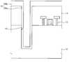
도 1은 본 발명의 일 실시예에 따른 반도체 소자를 단면도이다.1 is a cross-sectional view of a semiconductor device in accordance with an embodiment of the present invention.
도 1을 참조하면, 제1 기판(10) 상에 제1 회로 패턴(12)들이 구비된다. 상기 제1 기판(10)은 반도체 물질로 이루어진 기판 일 수 있으며, 일 예로, 단결정 실리콘 기판일 수 있다. 상기 제1 회로 패턴(12)들은 트랜지스터, 다이오드 등을 포함할 수 있다. 상기 제1 기판(10) 상에는 상기 제1 회로 패턴(12)들을 덮는 제1 층간 절연막(14)이 구비된다. 상기 제1 회로 패턴(12)들은 폴리실리콘으로 이루어지는 콘택들에 의해 전기적으로 연결될 수 있다.Referring to FIG. 1,
상기 제1 층간 절연막(14) 및 제1 기판(10)에는, 상기 제1 층간 절연막(14)을 관통하여 제1 기판(10) 내부까지 연장되는 비아홀(16)이 생성되어 있다. 상기 비아홀(16)의 깊이는 10 내지 100㎛이다. 바람직하게는, 상기 비아홀(16)은 30 내지 60㎛의 깊이를 갖는다. 또한, 상기 비아홀(16)의 직경은 1 내지 30㎛ 이며, 바람직하게는 1 내지 10㎛이다. 하나의 반도체 칩을 이루는 제1 기판(10)에는 상기 비아홀(16)이 복수개가 구비될 수 있다.Via
상기 비아홀(16)의 측벽 및 저면과 상기 제1 층간 절연막(14) 상부면 프로파일을 따라 절연막 구조물(18)이 구비된다. 상기 절연막 구조물(18)은 제1 절연막(18a) 및 제2 절연막(18b)을 포함한다. 상기 비아홀(16)의 측벽 및 저면에 위치하는 제1 절연막(18a)은 제1 기판(10)과 비아홀(16)내의 도전 물질 사이를 절연시키는 역할을 한다. 또한, 상기 제1 층간 절연막(14) 상부면에 위치하는 제2 절연막(18b)은 층간 절연막(ILD, Inter Layer Dielectric)의 역할을 한다. 이와 같이, 상기 제2 절연막(18b)이 층간 절연막의 일부로써의 기능을 하기 때문에, 상기 제1 층간 절연막(14) 및 상기 제2 절연막(18b)의 두께의 합이 상부 배선(34, 38) 아래에 위치하는 층간 절연막의 전체 두께가 된다.An insulating
상기 제1 기판(10)과 비아홀(16) 내의 도전 물질 사이의 기생 커패시턴스를 감소시키기 위하여 상기 절연막 구조물(18)은 저유전 물질로 이루어질 수 있다. 상기 절연막 구조물(18)은 실리콘 산화물 또는 탄소 도핑된 실리콘 산화물로 이루어질 수 있으며, 상기 실리콘 산화물은 다공성을 가질 수 있다.The insulating
또한, 상기 제1 기판(10)과 비아홀(16) 내의 도전 물질 사이의 기생 커패시턴스를 감소시키기 위하여 상기 절연막 구조물(18)이 두껍게 형성될 수 있다. 상기 절연막 구조물(18)이 1000Å보다 얇으면 절연 특성이 나빠지고, 상기 절연막 구조물(18)이 상기 비아홀 직경의 1/4의 두께보다 두꺼우면 상대적으로 비아홀(16)에 채워지는 도전 물질이 감소되어 저항이 증가되는 문제가 발생될 수 있다. 그러므로, 상기 절연막 구조물(18)은 1000Å보다 두껍고 상기 관통홀 직경의 1/4의 두께보다는 얇은 두께를 가질 수 있다.In addition, the insulating
또한, 상기 제1 및 제2 절연막들(18a, 18b)은 서로 다른 두께를 가질 수 있다. 상기 제2 절연막(18b)은 증착 시의 두께의 적어도 30%이상의 두께를 갖는다.In addition, the first and second insulating
상기 비아홀(16) 측벽 및 저면에 위치하는 제1 절연막(18a) 상에는 배리어 막 패턴(20a)이 구비된다. 상기 배리어 막 패턴(20a)은 Ta, TaN, Ti, TiN, Ru, Co, Ni, NiB, WN 등의 물질을 포함할 수 있다. 이들은 단독으로 사용되거나 또는 2 이상을 적층하여 사용할 수 있다.The
상기 배리어 막 패턴(20a) 상에는 상기 비아홀(16) 내부를 채우는 도전 패턴(22a)이 구비된다. 상기 도전 패턴(22a)은 저저항을 갖는 금속으로 이루어질 수 있다. 일 예로, 상기 도전 패턴(22a)은 구리(Cu) 또는 텅스텐을 포함할 수 있다. 본 실시예에서, 상기 도전 패턴(22a)은 저저항을 갖는 구리로 이루어진다. 즉, 상기 비아홀(16) 내에는 상기 배리어 막 패턴(20a) 및 도전 패턴(22a)으로 이루어지는 실리콘 관통 비아 콘택(24)이 구비된다.The
상기 실리콘 관통 비아 콘택(24)의 상부면은 상기 제1 층간 절연막(14) 상에 위치하는 제2 절연막(18b)의 상부면과 동일한 평면에 위치한다. 즉, 상기 실리콘 관통 비아 콘택(24)들 사이에는 상기 제2 절연막(18b)이 존재한다.An upper surface of the silicon through via
상기 실리콘 관통 비아 콘택(24) 및 제2 절연막(18b)의 상부면을 덮는 버퍼막(26)이 구비된다. 상기 버퍼막(26)은 상기 실리콘 관통 비아 콘택(24)의 도전 물질이 확산되는 것을 방지하는 역할을 한다. 특히, 상기 실리콘 관통 비아 콘택(26)이 구리를 포함하는 경우, 구리의 확산을 방지하기 위하여 상기 버퍼막(26)이 반드시 필요하다. 상기 버퍼막(26)은 실리콘 질화물, 실리콘 탄소 질화물 및 SiCON 등으로 이루어질 수 있으며, 이들은 단독 또는 2 이상이 적층된 형상을 가질 수 있다. 상기 버퍼막(26)은 300 내지 1000Å의 두께를 가질 수 있다.A
상기 제2 절연막(18b) 및 제1 층간 절연막(14)을 관통하여 상기 제1 회로 패턴(12)들과 전기적으로 연결되는 콘택 플러그(28)가 구비된다. 상기 콘택 플러그(28)의 상부면은 상기 실리콘 관통 비아 콘택(24) 상부면과 동일한 평면에 위치한다. 상기 콘택 플러그(28)는 금속 물질로 이루어질 수 있다. 일 예로, 상기 콘택 플러그(28)는 배리어 막 및 텅스텐을 포함할 수 있다. 상기 콘택 플러그(28)는 구리를 포함할 수도 있다.A
상기 버퍼막(26) 상에는 제1 금속간 절연막(IMD, Inter Metal Dielectric, 30)이 구비된다. 상기 제1 금속간 절연막(30)은 저유전율을 갖는 물질로 이루어질 수 있으며, 예를들어 실리콘 산화물, 탄소 도핑된 실리콘 산화물 등으로 이루어질 수 있다.A first intermetal dielectric (IMD, Inter Metal Dielectric) 30 is provided on the
상기 버퍼막(26) 및 제1 금속간 절연막(30)을 관통하면서 상기 실리콘 관통 비아 콘택(24) 및 콘택 플러그(28)와 각각 전기적으로 연결되는 제1 배선(34)이 구비된다. 상기 제1 배선(34)은 배리어 막 및 구리, 텅스텐등과 같은 금속막을 포함할 수 있다. 바람직하게는, 상기 제1 배선(34)은 배리어 막 및 저저항을 갖는 구리를 포함한다.A
또한, 상기 제1 금속간 절연막(30) 및 제1 배선(34) 상에, 상기 제2 금속간 절연막(36) 및 제2 배선(38)을 포함한다. 도시하지는 않았지만, 상기 제2 금속간 절연막(36) 및 제2 배선(38) 상에 제3 금속간 절연막 및 제3 배선을 더 포함할 수 있다.In addition, the second intermetallic insulating
설명한 것과 같이, 본 발명에 따른 반도체 소자는 실리콘 관통 비아 콘택과 기판 간의 절연 특성이 우수하고, 기생 커패시턴스가 감소된다. 또한, 반도체 소자에 포함되는 실리콘 관통 비아 콘택은 저저항을 갖고 신호 전달 특성이 우수하다.
As described, the semiconductor device according to the present invention has excellent insulation properties between the silicon through via contact and the substrate, and the parasitic capacitance is reduced. In addition, the silicon through via contact included in the semiconductor device has low resistance and excellent signal transmission characteristics.
도 2 내지 도 10은 도 1에 도시된 반도체 소자를 제조하는 제1 방법을 나타내는 단면도들이다.2 to 10 are cross-sectional views illustrating a first method of manufacturing the semiconductor device illustrated in FIG. 1.
도 2를 참조하면, 제1 기판(10) 상에 제1 회로 패턴(12)들을 형성한다. 상기 제1 회로 패턴(12)들은 CMOS 트랜지스터, 다이오드 등을 포함할 수 있다. 또한, 상기 제1 기판(10) 상에 상기 제1 회로 패턴(12)들을 덮는 제1 층간 절연막(14)을 형성한다. 후속 공정에서, 상기 제1 층간 절연막(14) 상에 절연막 구조물이 더 형성되므로, 상기 제1 층간 절연막(14)은 추가적으로 형성될 절연막 구조물의 두께를 고려하여 배선(metal interconnection) 아래에 위치하는 전체 층간 절연막의 목표 두께보다 얇게 형성한다.Referring to FIG. 2,
일반적으로, 상부의 배선 이 전의 반도체 제조 공정을 FEOL(front-end-of-line)공정이라 하고, 배선부터 이 후의 반도체 제조 공정을 BEOL(Back-end-of-line)공정이라 한다. 아래에 설명하는 것과 같이, 본 실시예에서는 상기 제1 회로 패턴(12)들을 형성하고 난 다음, 상기 BEOL 공정을 수행하기 이 전에 실리콘 관통 비아 콘택을 형성한다.Generally, the semiconductor manufacturing process before the upper wiring is called a front-end-of-line (FEOL) process, and the semiconductor manufacturing process after wiring is called a BEOL (back-end-of-line) process. As described below, in the present embodiment, after the
도 3을 참조하면, 상기 제1 층간 절연막(14) 상에 포토레지스트막(도시안됨)을 형성하고, 상기 포토레지스트막을 패터닝하여 포토레지스트 패턴을 형성한다. 상기 포토레지스트 패턴은 약 2 내지 5㎛의 두께를 가질 수 있다.Referring to FIG. 3, a photoresist film (not shown) is formed on the first
상기 포토레지스트 패턴을 식각 마스크로 사용하여 상기 제1 층간 절연막(14)을 식각하고 계속하여 제1 기판(10)을 건식 식각한다. 이로써, 상기 제1 층간 절연막(14)을 관통하고 제1 기판(10) 내부까지 연장되는 비아홀(16)을 형성한다. 상기 비아홀(16) 내에는 후속 공정을 통해 실리콘 관통 비아 콘택이 형성된다.The first
상기 비아홀(16)의 깊이가 10㎛보다 작으면, 실리콘 관통 비아 콘택의 깊이가 너무 작아져 적층형 반도체 소자로 제조되기가 어렵다. 또한, 상기 비아홀(16)의 깊이가 100㎛보다 크면, 상기 비아홀(14) 내부에 도전 물질을 채우는 것이 용이하지 않다. 그러므로, 상기 비아홀(16)은 10 내지 100㎛의 깊이를 가지며, 바람직하게는 30 내지 60㎛의 깊이를 갖는다.If the depth of the via
또한, 상기 비아홀(16)의 직경이 1㎛보다 작으면 비아홀(16) 내부에 도전 물질을 채우는 것이 용이하지 않다. 또한, 상기 비아홀(16)의 직경이 30㎛ 크면, 상기 비아홀(16)이 차지하는 수평 면적이 증가되어 바람직하지 않다. 그러므로, 상기 비아홀(16)은 5 내지 30㎛의 직경을 가지며, 바람직하게는 1 내지 10㎛의 직경을 갖는다.In addition, when the diameter of the via
상기 비아홀(16)을 형성한 다음에, 상기 포토레지스트 패턴을 제거한다.After the via
도 4를 참조하면, 상기 비아홀(16) 측벽, 저면 및 제1 층간 절연막(14) 상부면의 프로파일을 따라 절연막 구조물(18)을 형성한다.Referring to FIG. 4, the insulating
상기 비아홀(16) 내에 형성되는 제1 절연막(18a)은 상기 제1 기판(10)과 비아홀(16) 내의 도전 물질을 절연시킨다. 또한, 상기 제1 층간 절연막(14) 상부면에 형성되는 절연막 구조물(18)의 제2 절연막(18b)은 층간 절연막의 일부로 제공된다. 상기 제1 기판(10)과 실리콘 관통 비아 콘택간의 기생 커패시턴스를 감소시키기 위하여, 상기 절연막 구조물(18)은 저유전율을 갖는 절연 물질을 증착하여 형성할 수 있다. 상기 절연막 구조물(18)은 실리콘 산화물 또는 탄소 도핑된 실리콘 산화물로 형성할 수 있다. 일 예로, 상기 절연막 구조물(18)은 플라즈마 산화 공정을 통해 형성하거나 또는 화학기상 증착 공정을 통해 형성할 수 있으며, 스텝 커버러지 특성이 우수한 TEOS막, 오존 TEOS막 등으로 형성할 수 있다.The first insulating
상기 절연막 구조물(18)은 1000Å보다 두껍고 상기 관통홀 직경의 1/4의 두께보다는 얇은 두께를 갖도록 형성할 수 있다. 또한, 상기 절연막 구조물(18)은 상기 제1 절연막(18a) 두께보다 상기 제2 절연막(18b)의 두께가 더 두껍게 되도록 형성하는 것이 바람직하다. 상기 제2 절연막(18b)의 두께가 두꺼운 경우, 제1 층간 절연막(14)의 두께를 더욱 감소시킬 수 있다. 일 예로, 상기 제2 절연막(18b) 및 제1 절연막(18a)의 두께비는 1 : 0.3 내지 0.9 인 것이 바람직하다.The insulating
도 5를 참조하면, 상기 절연막 구조물(18) 상에 배리어 막(20)을 형성한다. 상기 배리어 막(20)은 Ta, TaN, Ti, TiN, Ru, Co, Ni, NiB, WN 등의 물질로 형성할 수 있으며, 이들은 단독 또는 2 이상이 적층될 수 있다. 상기 배리어 막(20)은 100 내지 3000Å의 두께로 형성할 수 있다.Referring to FIG. 5, a
상기 배리어 막(20) 상에 시드막(도시안됨)을 형성한다. 상기 시드막은 후속의 도전막(22)을 형성하기 위한 도금 공정에서 전극으로 사용되는 막이다. 일 예로, 상기 시드막은 물리 기상증착법을 통해 구리를 증착시켜 형성할 수 있다.A seed layer (not shown) is formed on the
상기 시드막 상에 상기 비아홀(16) 내부를 채우도록 도전막(22)을 형성한다. 상기 도전막(22)은 저저항의 금속 물질로 형성된다. 일 예로, 상기 도전막(22)은 전해 도금법, 무전해 도금법, 전자 융합법(Electrografting), 물리기상증착법 등에 의해 구리를 증착시켜 형성할 수 있다. 상기 도전막(22)을 형성하고 난 다음, 상기 도전막(22)을 열처리하는 공정을 더 수행할 수도 있다. 이와는 다른 예로, 상기 도전막(22)은 화학기상 증착법에 의해 텅스텐을 증착시켜 형성할 수도 있다. 그러나, 상기 도전막(22)은 상기 텅스텐에 비해 저저항을 갖는 구리로 형성하는 것이 바람직하다.A
도 6을 참조하면, 상기 도전막(22) 및 배리어 막(20)을 화학기계적 연마공정을 통해 연마하여 실리콘 관통 비아 콘택(24)을 형성한다. 상기 실리콘 관통 비아 콘택(24)은 배리어 막 패턴(20a) 및 도전 패턴(22a)을 포함한다.Referring to FIG. 6, the
상기 연마 공정을 수행하면, 상기 제2 절연막(18b)의 상부면이 노출된다. 즉, 상기 연마 공정을 완료하더라도 상기 제1 층간 절연막(14) 상에는 제2 절연막(18b)이 남아있다. 그러나, 상기 연마 공정 시에 상기 제2 절연막(18b)을 일부 두께만큼 제거될 수도 있다. 상기 연마 공정을 수행한 이 후에 남아있는 상기 제2 절연막(18b)이 증착 시 제2 절연막(18b)의 두께의 30%이하인 경우에는 상기 제2 절연막(18b)이 층간 절연막으로써의 기능을 할 정도로 충분한 두께를 갖지 못한다. 그러므로, 연마 공정 후의 상기 제2 절연막(18b)은 증착 시 제2 절연막(18b) 두께의 30% 이상의 두께를 갖는 것이 바람직하다.When the polishing process is performed, an upper surface of the second insulating
따라서, 상기 실리콘 관통 비아 콘택(24)의 상부면은 상기 제2 절연막(18b)의 상부면과 동일한 평면에 위치하게 된다.Therefore, the top surface of the through silicon via
상기 연마 공정에서 상기 절연막 구조물(18)을 남기기 때문에, 상기 연마 공정에서 제거하여야 하는 막의 두께가 감소된다. 그러므로, 상기 연마 공정 에 의한 어택이 감소하게 되고, 상기 연마 공정을 수행한 후 잔류하는 막 또는 패턴의 평탄도가 매우 높아지게 된다. 또한, 상기 연마 공정 시간도 단축된다.Since the insulating
일반적인 공정에서는, 상기 절연막 구조물(18)을 연마에 의해 완전하게 제거하므로, 상기 절연막 구조물(18)의 연마 두께가 증가하면 연마 공정이 용이하지 않아서 상기 절연막 구조물(18)의 두께를 충분하게 증가시킬 수 없있다. 그러나, 본 실시예의 경우에는 상기 절연막 구조물(18)이 연마에 의해 거의 또는 전혀 제거되지 않으므로, 상기 절연막 구조물(18)의 두께를 충분히 증가시킬 수 있다.In the general process, since the insulating
이에 더하여, 상기 연마 공정을 수행할 때 상기 실리콘 관통 비아 콘택(24) 이외의 콘택 플러그 또는 하부 배선들이 상기 절연막 구조물(18) 표면 상에 노출되지 않는다. 그러므로, 상기 연마 공정에 의해 상기 콘택 플러그 및 하부 배선이 손상되지 않는다.In addition, no contact plugs or bottom wires other than the through silicon via
도 7을 참조하면, 상기 절연막 구조물(18) 및 실리콘 관통 비아 콘택(24)을 덮는 버퍼막(26)을 형성한다. 상기 버퍼막(26)은 절연 물질로 이루어지며, 상기 실리콘 관통 비아 콘택(24)에 포함되는 금속 물질의 확산을 억제시키기 위하여 제공된다. 상기 버퍼막(26)은 실리콘 질화물, 실리콘 탄소 질화물, SiCON 등으로 형성할 수 있으며, 이들은 단독 또는 2 이상을 적층하여 형성할 수 있다. 상기 버퍼막(26)은 300 내지 1000Å의 두께로 형성할 수 있다.Referring to FIG. 7, a
도 8을 참조하면, 상기 버퍼막(26), 절연막 구조물(18) 및 제1 층간 절연막(14)을 관통하여 상기 제1 회로 패턴(12)의 일부와 전기적으로 연결되는 콘택 플러그(28)를 형성한다. 상기 콘택 플러그(28)는 상부 배선 아래에 위치한다. 그러므로, 상기 콘택 플러그(28)를 형성함으로써, FEOL 공정이 완료된다.Referring to FIG. 8, a
구체적으로, 상기 버퍼막(26), 절연막 구조물(18) 및 제1 층간 절연막(14)을 순차적으로 식각하여, 상기 버퍼막(26), 절연막 구조물(18) 및 제1 층간 절연막(14)을 관통하는 콘택홀을 형성한다. 상기 콘택홀의 측벽 및 저면을 따라 배리어 막(도시안함) 및 도전막(도시안함)을 형성하고, 상기 버퍼막(26)의 상부면이 노출되도록 상기 도전막을 화학 기계적으로 연마하여 콘택 플러그(28)를 형성한다. 상기 도전막은 구리 또는 텅스텐을 포함할 수 있다. 본 실시예에서, 상기 도전막은 텅스텐으로 형성할 수 있다.Specifically, the
상기에서 설명한 것과 같이, 본 실시예에서는 상기 실리콘 관통 비아 콘택(24)은 상기 FEOL 공정을 수행하는 과정 중에 형성된다. 그리고, 상기 콘택 플러그(28)는 상기 실리콘 관통 비아 콘택(24)을 형성한 이 후에 형성한다.As described above, in the present embodiment, the silicon through via
일반적으로, 상기 콘택 플러그(28)를 형성하여 FEOL 공정을 완료한 다음에 실리콘 관통 비아 콘택(24)을 형성하는 경우에는, 상기 실리콘 관통 비아 콘택(24)을 형성하는 과정에서 콘택 플러그(28)에 어택이 거해질 수 있었다. 그러나, 본 실시예의 경우, 실리콘 관통 비아 콘택(24)을 형성한 다음 콘택 플러그(28)가 형성되므로, 콘택 플러그(28)에 어택이 가해지지 않는다. 또한, 본 실시예의 경우, 상기 실리콘 관통 비아 콘택(24) 상에는 버퍼막(26)이 형성되어 있다. 때문에, 상기 콘택 플러그(28)를 형성할 때, 상기 버퍼막(26)이 상기 실리콘 관통 비아 콘택(24)을 보호하고 있으므로 상기 실리콘 관통 비아 콘택(24)에는 어택이 거의 가해지지 않는다.In general, in the case of forming the through silicon via
그러므로, 상기 실리콘 관통 비아 콘택(24) 및 콘택 플러그(28)는 양호한 도전 특성을 가질 수 있다.Therefore, the through silicon via
도 9를 참조하면, 상기 버퍼막(26) 및 콘택 플러그(28) 상에 제1 금속간 절연막(IMD, Inter Metal Dielectric, 30)을 형성한다. 이 후, 상기 제1 금속간 절연막(30), 상기 버퍼막(26) 및 상기 콘택 플러그(28)의 일부분을 식각하여 상기 실리콘 관통 비아 콘택(24) 및 콘택 플러그(28)의 상부면을 노출하는 제1 개구(32)들을 형성한다. 상기 제1 개구(32)들이 형성되는 부위는 제1 배선(34)을 형성하기 위한 부위가 된다.Referring to FIG. 9, a first intermetal dielectric (IMD) 30 is formed on the
도 10을 참조하면, 상기 제1 개구(32) 내부 측벽 및 저면을 따라 배리어 막(도시안함) 및 도전막(도시안함)을 형성한다. 상기 도전막은 구리를 포함할 수 있다. 상기 도전막은 전해 도금법, 무전해 도금법, 무전해 도금법, 전자 융합법(Electrografting), 물리기상증착법 등에 의해 구리를 증착시켜 형성할 수 있다. 이 후, 상기 도전막 및 배리어 막을 연마함으로써, 상기 제1 개구(32) 내부에 제1 배선(34)을 형성한다.Referring to FIG. 10, a barrier film (not shown) and a conductive film (not shown) are formed along sidewalls and bottom surfaces of the
본 실시예에서, 상기 제1 금속간 절연막(30)은 상기 실리콘 관통 비아 콘택(24) 및 콘택 플러그(28) 상에 형성되어 있으므로, 상기 제1 개구(32)의 저면에 상기 실리콘 관통 비아 콘택(24) 및 콘택 플러그(28)가 노출될 수 있다. 따라서, 상기 실리콘 관통 비아 콘택(24)과 제1 배선(34)의 연결 불량 및 콘택 플러그(28)와 제1 배선(34)의 연결 불량이 거의 발생하지 않게 된다.In the present embodiment, since the first intermetallic insulating
다시, 도 1을 참조하면, 상기 제1 배선(34) 및 제1 금속간 절연막(30) 상에 제2 금속간 절연막(36) 및 제2 배선(38)을 형성한다.Referring back to FIG. 1, a second intermetallic insulating
구체적으로, 상기 제1 배선(34) 및 제1 금속간 절연막(30) 상에 제2 금속간 절연막(36)을 형성한다. 상기 제2 금속간 절연막(36)에 제2 개구(도시하지 않음)를 형성하고, 상기 제2 개구에 금속을 사용하여 제2 배선(36)을 형성한다.Specifically, a second intermetallic insulating
도시하지는 않았지만, 동일한 방법으로 상기 제2 금속간 절연막(36) 및 제2 배선(38) 상에 제3 개구(도시하지 않음)을 형성하고, 이를 채우는 제3 금속간 절연막 및 제3 배선을 더 형성할 수 있다. 이로써, 도 1에 도시된 반도체 소자를 완성한다.Although not shown, a third opening (not shown) is formed on the second intermetallic insulating
설명한 것과 같이, 본 발명에 따르면 실리콘 관통 비아 콘택과 기판간의 절연 특성이 우수하며, 기생커패시턴스가 감소된 반도체 소자를 제조할 수 있다. 또한, 저저항을 갖고 신호 전달 특성이 우수한 콘택 플러그 및 실리콘 관통 비아 콘택을 형성할 수 있다.
As described above, according to the present invention, a semiconductor device having excellent insulating properties between the silicon through via contact and the substrate and having reduced parasitic capacitance can be manufactured. In addition, it is possible to form a contact plug and a through-silicon via contact having low resistance and excellent signal transmission characteristics.
도 11 및 12는 도 1에 도시된 반도체 소자를 제조하는 제2 방법을 나타내는 단면도들이다.11 and 12 are cross-sectional views illustrating a second method of manufacturing the semiconductor device illustrated in FIG. 1.
이하에서 설명하는 제2 방법은 일부 공정이 더 추가된 것을 제외하고는 상기 제1 방법과 동일하다. 그러므로, 동일한 공정에 대한 설명은 생략한다.The second method described below is the same as the first method except that some processes are further added. Therefore, description of the same process is omitted.
먼저, 도 2 내지 도 6을 참조로 설명한 공정을 수행함으로써, 관통 비아 콘택(24)을 형성한다.First, the through via
설명한 것과 같이, 상기 실리콘 관통 비아 콘택(24)의 저항을 감소시키기 위하여, 상기 실리콘 관통 비아 콘택(24)은 구리를 포함할 수 있다. 그런데, 상기 구리는 텅스텐에 비해 열팽창계수가 매우 높다. 또한, 상기 제1 기판(10)을 이루는 실리콘과 구리간의 열팽창 계수의 미스매치가 매우 크다. 그러므로, 후속의 열을 수반하는 공정들이 수행될 때, 상기 구리를 포함하는 실리콘 관통 비아 콘택(24)은 열팽창에 의해 상부면이 위로 돌출할 수 있다. 본 실시예는 상기 실리콘 관통 비아 콘택(24)의 상부면이 위로 돌출하는 것을 미연에 방지하기 위한 공정들이 추가된 반도체 소자의 제조 방법이다.As described, in order to reduce the resistance of the through silicon via via 24, the through silicon via 24 may include copper. However, the copper has a very high coefficient of thermal expansion compared to tungsten. In addition, the mismatch of the coefficient of thermal expansion between silicon and copper constituting the
도 11을 참조하면, 상기 실리콘 관통 비아 콘택(24)이 형성되어 있는 구조에 대해 열처리 공정을 수행함으로써, 상기 실리콘 관통 비아 콘택(24)의 상부면을 인위적으로 돌출시킨다. 즉, 상기 실리콘 관통 비아 콘택(24)에 열을 가하여 상기 도전 패턴(22a)의 부피를 팽창시킴으로써 팽창된 도전 패턴(22b)을 형성한다. 이에 따라, 팽창된 실리콘 관통 비아 콘택(24b)이 형성된다.Referring to FIG. 11, an upper surface of the silicon through via
상기 열처리 공정이 100℃이하에서 수행되는 경우에는 상기 실리콘 관통 비아 콘택(24)이 충분하게 열팽창될 수 없다. 또한, 상기 열처리 공정이 600℃이상에서 수행되는 경우에는 상기 실리콘 관통 비아 콘택(24)에 포함된 구리가 열화될 수 있다. 그러므로, 상기 열처리 공정은 100 내지 600℃의 온도에서 수행되는 것이 바람직하다.When the heat treatment process is performed at 100 ° C. or lower, the silicon through via
도 12를 참조하면, 상기 팽창된 실리콘 관통 비아 콘택(24b)의 상부면이 평탄해지도록 상기 팽창된 실리콘 관통 비아 콘택(24b)을 화학 기계적으로 연마한다. 상기 연마 공정을 통해, 평탄한 상부면을 갖는 실리콘 관통 비아 콘택(24) 및 절연막 구조물(18)이 형성된다. 또한, 상기 실리콘 관통 비아 콘택(24)은 열처리 공정을 통해 충분하게 열팽창되었으므로, 후속에서 열 공정이 수행되더라도 상부면이 돌출되는 등의 문제가 발생되지 않는다.Referring to FIG. 12, the expanded silicon through via
계속하여, 도 7 내지 도 10을 참조로 설명한 공정을 동일하게 수행함으로써, 도 10에 도시된 반도체 소자를 제조할 수 있다.
Subsequently, by performing the same process described with reference to FIGS. 7 to 10, the semiconductor device illustrated in FIG. 10 may be manufactured.
도 13은 본 발명의 일 실시예에 따른 적층형 반도체 소자를 나타내는 단면도들이다.13 is a cross-sectional view illustrating a stacked semiconductor device according to an exemplary embodiment of the present invention.
상기 적층형 반도체 소자는 관통 비아 콘택이 포함된다.The stacked semiconductor device includes a through via contact.
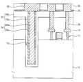
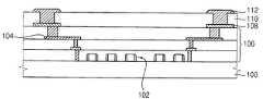
도 13을 참조하면, 적층형 반도체 소자는 제1 반도체 칩(150), 제2 반도체 칩(152) 및 접촉 패턴(112)을 포함한다.Referring to FIG. 13, the stacked semiconductor device includes a
상기 제1 반도체 칩(150)에 포함되는 소자는 메모리 소자 또는 로직 소자일 수 있다. 다른 예로, 상기 제1 반도체 칩(150)에 포함되는 소자는 이미지 소자일 수도 있다. 일 예로, 상기 제1 반도체 칩(150)은 제1 기판(10a)에 형성되며, 실리콘 관통 비아 콘택(55)의 저면 부위가 제1 기판(10a)의 저면에 노출되어 있는 것을 제외하고는 도 1에 도시된 반도체 소자와 동일한 구성을 가질 수 있다. 이에 더하여, 반복 적층된 배선들 중에서 최상부의 제3 배선(42) 및 제3 금속간 절연막(40) 상에는 보호막(44)이 구비될 수 있다. 상기 보호막(44)에는 상기 최상부 제3 배선(42)의 일부 영역을 노출하는 제4 개구(도시하지 않음)가 생성되어 있을 수 있다.The device included in the
이하에서는, 상기 제1 반도체 칩(150)에 대해 간단히 설명한다. 상기 제1 반도체 칩(150)은 제1 기판(10a), 상기 제1 기판(10a) 상에 구비되는 제1 회로 패턴들(12), 하부 배선들(28), 제1 층간 절연막(14) 및 절연막 패턴 구조물(19)을 포함한다. 상기 절연막 패턴 구조물(19)의 상부면으로부터 상기 제1 기판(10a)을 관통하는 실리콘 관통 비아 콘택(55)을 포함한다. 상기 실리콘 관통 비아 콘택(55) 및 절연막 패턴 구조물(19) 상에는 상부 배선(34, 38, 42) 및 금속간 절연막들(30, 36, 40)이 구비된다. 또한, 상기 최상부의 제3 배선(42)을 덮는 보호막(44)이 구비된다.Hereinafter, the
상기 제1 기판(10a)은 단결정 실리콘 기판일 수 있다. 상기 제1 기판(10a)은 10 내지 100㎛의 두께를 갖는다. 상기 제1 기판(10a)의 저면이 실리콘 관통 비아 콘택(55)의 저면과 동일한 평면에 위치할 수 있다. 또는, 상기 제1 기판(10a)은 상기 실리콘 관통 비아 콘택(55)이 상기 제1 기판(10a) 저면 아래로 돌출되도록 위치할 수 있다. 따라서, 상기 제1 기판(10a) 저면에는 상기 관통 실리콘 바이 콘택(55)의 저면이 노출된다.The
이하에서는, 상기 제1 기판(10a)을 관통하는 실리콘 관통 비아 콘택을 설명한다.Hereinafter, a silicon through via contact penetrating the
상기 제1 기판(10a)에는 제1 기판(10a) 상부면으로부터 저면까지 연장되어 상기 제1 기판(10a)을 관통하는 비아홀(16)이 구비된다. 상기 비아홀(16)은 1 내지 30㎛의 직경을 가지며, 바람직하게는 1 내지 10㎛의 직경을 갖는다.The
상기 비아홀(16)의 측벽 및 상기 제1 층간 절연막(14) 상에는 절연막 패턴 구조물(19)이 구비된다. 절연막 패턴 구조물(19)은 제1 절연막 패턴(18c) 및 제2 절연막 패턴(18b)을 포함한다. 그러나, 상기 절연막 패턴 구조물(19)은 상기 비아홀(16)의 저면에는 구비되지 않는다. 즉, 상기 비아홀(16) 측벽에는 상, 하부면이 오픈된 원통 형상의 제1 절연막 패턴(18c)이 구비된다. 상기 제1 절연막 패턴(18c)은 상기 제1 기판(10a)과 실리콘 관통 비아 콘택(55)간을 절연시키는 역할을 한다. 상기 원통 형상의 제1 절연막 패턴(18c) 상에는 배리어 막 패턴(50b) 및 시드 패턴(도시안됨)이 구비된다. 또한, 상기 제1 층간 절연막(14) 상에 구비되는 제2 절연막 패턴(18b)은 층간 절연막의 역할을 한다.An insulating
상기 시드 패턴 상에 상기 비아홀(16) 내부를 채우는 도전 패턴(52a)이 구비된다. 상기 도전 패턴(52a)은 구리를 포함할 수 있다. 상기 도전 패턴(52a)의 저면은 상기 제1 기판(10a) 저면에 노출된 형상을 가질 수 있다. 또한, 상기 도전 패턴(52a)의 저면은 상기 제1 기판(10a) 저면과 동일한 평면에 위치하거나 제1 기판(10a) 저면보다 돌출될 수 있다.A
상기 제1 기판(10a) 상에 구비되는 상부 배선들(34, 38, 42)을 덮는 제1 보호막(44)이 구비된다. 상기 제1 보호막(44)은 절연 물질로 이루어지며, 일 예로, 폴리이미드 물질을 포함할 수 있다. 상기 제1 보호막(44)은 패드 전극으로 제공되는 최상부의 제3 배선(42)의 적어도 일부를 노출시키는 제4 개구(46)가 포함되어 있다. 지금부터는 제3 배선(42)을 제1 패드 전극(42)으로도 호칭한다.The
상기 제1 패드 전극(42)에는 솔더(48)가 구비될 수 있으며, 상기 솔더(48)는 인쇄 회로 기판과 접촉될 수 있다. 이와는 달리, 도시하지는 않았지만, 와이어 본딩에 의해 상기 제1 패드 전극(42)이 리드 프레임과 전기적으로 연결될 수도 있다.
한편, 제2 반도체 칩(152)은 제2 기판(100), 상기 제2 기판(100) 상에 구비되는 제2 회로 패턴들(102), 배선들(104), 제2 층간 절연막들(106), 상기 관통 비아 콘택(55)을 통해 신호가 인가되는 제2 패드 전극(108)을 포함한다.Meanwhile, the
상기 제2 반도체 칩(152)에 포함된 반도체 소자는 상기 제1 반도체 칩(150)에 포함된 것과 동일한 반도체 소자일 수도 있고, 서로 다른 반도 소자일 수도 있다.The semiconductor device included in the
도시된 것과 같이, 상기 최상부에 형성된 층간 절연막(106)에는 배선들(104)과 연결되는 제2 패드 전극(108)이 구비된다. 상기 제2 패드 전극(108)은 상기 제1 기판(10a)의 관통 비아 콘택(55)의 저면과 접합되어 전기적으로 연결되어 있다.As shown in the drawing, the
상기 최상부의 층간 절연막(106) 및 제2 패드 전극(108) 상에는 제2 보호막(110)이 구비된다. 상기 제2 보호막(110)은 폴리이미드 물질로 이루어질 수 있다. 이 때, 상기 제2 패드 전극(108)에서 상기 관통 비아 콘택(55)의 저면과 접촉되는 부위에는 개구가 생성되어 있다.The
상기 제1 반도체 칩(150)에 포함된 관통 비아 콘택(55)과 상기 제2 반도체 칩(152)에 포함된 제2 패드 전극(108) 사이에는 도전성을 갖는 접촉 패턴(112)이 개재되고, 상기 접촉 패턴(112)에 의해 상기 관통 비아 콘택(55) 및 제2 패드 전극(108)이 접착되어 있다. 상기 접촉 패턴(112)으로 사용될 수 있는 물질의 예로는 은(Ag) 솔더 페이스트를 들 수 있다.A
즉, 본 실시예에 따른 반도체 소자는 제1 및 제2 칩이 적층된 구조를 가지며, 하나의 관통 비아 콘택을 통해 상기 제1 및 제2 칩이 전기적으로 연결된다. 또한, 본 실시예에 따른 적층형 소자는 기생 커패시턴스가 감소되어 빠른 신호 전달 속도를 갖는다.That is, the semiconductor device according to the present exemplary embodiment has a structure in which first and second chips are stacked, and the first and second chips are electrically connected through one through via contact. In addition, the stacked device according to the present embodiment has a high signal transmission speed due to the reduction of parasitic capacitance.
도시하지는 않았지만, 제1 칩과 동일한 구조의 실리콘 관통 비아 콘택을 포함하는 3개 이상의 칩들이 수직으로 적층될 수 있다. 이 때, 각 칩 내에 관통 비아 콘택의 저면은 다른 칩의 최상부 패드 전극과 전기적으로 접촉되는 형상을 가질 수 있다.
Although not shown, three or more chips including silicon through via contacts having the same structure as the first chip may be stacked vertically. At this time, the bottom surface of the through via contact in each chip may have a shape in electrical contact with the top pad electrode of the other chip.
도 14 내지 도 19는 도 13에 도시된 적층형 반도체 소자의 제조 방법을 나타내는 단면도들이다.14 to 19 are cross-sectional views illustrating a method of manufacturing the stacked semiconductor device illustrated in FIG. 13.
도 14를 참조하면, 예비 제1 기판(10) 상에 제1 회로 패턴들(12), 제1 층간 절연막(14) 및 비아홀(16)을 형성한다. 상기 비아홀(16)의 내부 표면 및 제1 층간 절연막(14) 상에 절연막 구조물(18)을 형성한다. 상기 제1 층간 절연막(14) 및 절연막 구조물(18)을 관통하고, 상기 예비 제1 기판(10) 내부로 연장되는 예비 실리콘 관통 비아 콘택(54)을 형성한다. 상기 예비 관통 비아 콘택(54)은 도 1의 실리콘 관통 비아 콘택(24)과 동일한 구조를 갖는다. 즉, 상기 예비 실리콘 관통 비아 콘택(54)은 예비 배리어 막 패턴(50a) 및 도전 패턴(52a)를 포함한다. 상기 도전 패턴(52a)은 구리로 이루어질 수 있다. 상기에서 설명한 구조물들은 도 2 내지 도 6을 참조로 설명한 것과 동일한 공정으로 형성될 수 있다.Referring to FIG. 14,
도 15를 참조하면, 상기 절연막 구조물(18) 및 예비 실리콘 관통 비아 콘택(54)의 상부면을 덮는 버퍼막(26)을 형성한다. 상기 버퍼막(26)은 300 내지 1000Å의 두께로 형성할 수 있다. 상기 버퍼막(26), 절연막 구조물(18) 및 제1 층간 절연막(14)을 관통하는 콘택 플러그(28)를 형성한다. 상기 설명한 공정들은 도 7 및 도 8을 참조로 설명한 것과 동일하게 수행할 수 있다.Referring to FIG. 15, a
도 16을 참조하면, 상기 콘택 플러그(28) 상에 상부 배선들(34, 38, 42)을 형성한다.Referring to FIG. 16,
구체적으로, 상기 버퍼막(26) 상에 제1 금속간 절연막(30)을 형성한다. 이 후, 상기 제1 금속간 절연막(30) 및 상기 버퍼막(26)의 일부분을 식각하여 상기 예비 실리콘 관통 비아 콘택(54) 및 콘택 플러그(28)의 상부면을 노출하는 제1 개구들을 형성한다. 상기 제1 개구 내부에 제1 배선(34)을 형성한다. 상기 제1 배선(34) 및 제1 금속간 절연막(30) 상에, 동일한 방법으로 제2 금속간 절연막(36), 제2 배선(38), 제3 금속간 절연막(40) 및 제3 배선(42)을 형성한다.Specifically, a first intermetallic insulating
또한, 상부 배선들(34, 38, 42)을 덮는 제1 보호막(44)을 형성한다. 상기 제1 보호막(44)은 폴리이미드 물질을 포함할 수 있다. 상기 제1 보호막(44)의 일부분을 제거하여 최상부의 제3 배선(42)을 노출시키는 제4 개구(46)를 형성한다.In addition, the
도 17을 참조하면, 상기 예비 제1 기판(10), 절연막 구조물(18) 및 예비 배리어막 패턴(50a) 의 저면을 그라인딩을 통해 제거하여, 상기 예비 관통 비아 콘택(54)의 도전 패턴(52a)의 저면을 노출시킨다. 상기 공정을 통해, 예비 제1 기판(10)보다 얇은 제1 기판(10a) 및 저면에 도전 패턴(52a)이 노출된 실리콘 관통 비아 콘택(55)을 형성한다.Referring to FIG. 17, the bottom surfaces of the preliminary
구체적으로, 상기 예비 관통 비아 콘택(54)의 저면과 상기 예비 제1 기판(10)의 저면 사이의 거리가 수㎛ 정도로 가까워지도록 상기 예비 제1 기판(10)을 그라인딩한다. 계속하여, 상기 예비 관통 비아 콘택(54) 저면의 절연막 구조물(18)이 노출되도록 예비 제1 기판(10)을 식각한다. 다음에, 상기 저면에 노출된 절연막 구조물(18) 및 예비 제1 기판(10)을 함께 식각하여, 상기 도전 패턴(52a)이 노출되는 제1 기판(10a)을 형성한다. 이 때, 상기 도전 패턴(52a)의 저면은 상기 제1 기판(10a) 저면과 동일한 평면에 위치할 수도 있고, 상기 제1 기판(10a) 저면보다 돌출될 수도 있다.Specifically, the preliminary
상기 연마 및 식각 공정을 수행하면, 상기 예비 실리콘 관통 비아 콘택(54)에 포함된 절연막 구조물(18)의 저면은 제거되어 절연막 패턴 구조물(19)을 형성하며, 절연막 패턴 구조물(19)의 제1 절연막 패턴(18c)은 비아홀(16)의 내측벽을 둘러싸는 형상을 갖는다.When the polishing and etching process is performed, the bottom surface of the insulating
한편, 적층형 소자의 전체 두께를 감소시키기 위해서는 상기 예비 실리콘 관통 비아 콘택(54)의 높이가 낮아지는 것이 바람직하다. 그러나, 상기 예비 실리콘 관통 비아 콘택(54)의 높이가 낮아질수록, 상기 그라인딩 및 식각을 통해 제거되어야 할 상기 예비 제1 기판(10)의 두께는 더욱 증가하게 된다. 때문에, 상기 예비 실리콘 관통 비아 콘택(54)의 높이는 기판 그라인딩 공정 편차 등을 고려하여 설정될 수 있다.On the other hand, in order to reduce the overall thickness of the stacked device, it is preferable that the height of the preliminary silicon through via
도 18을 참조하면, 상기 제1 보호막(44)에 형성된 제4 개구(46) 내에 솔더(48)를 형성한다. 이로써, 제1 기판(10a)에 실리콘 관통 비아 콘택(55)을 포함하는 제1 반도체 소자가 완성된다.Referring to FIG. 18,
도 19를 참조하면, 제2 기판(100) 상에 상기 제1 반도체 소자와 접합되기 위한 제2 반도체 소자를 형성한다. 구체적으로, 상기 제2 기판(100) 상에 제2 회로 패턴들(102), 배선들(104) 및 제2 층간 절연막들(106)을 형성한다.Referring to FIG. 19, a second semiconductor device is formed on the
상기 제2 층간 절연막(106)의 최상부에 상기 배선들(104)과 전기적으로 연결되는 제2 패드 전극(108)을 형성한다. 상기 제2 패드 전극(108)은 상기 제1 기판(10a)에 형성된 실리콘 관통 비아 콘택(55)과 각각 대향하도록 배치된다.A
상기 제2 패드 전극(108) 및 최상부의 제2 층간 절연막(106)을 덮는 제2 보호막(110)을 형성한다. 다음에, 상기 제2 패드 전극(108)에서 신호가 인가되는 부위의 상부면에 위치하는 제2 보호막(110)을 제거하여 제5 개구를 형성한다. 상기 제2 기판(100)의 제2 패드 전극(108) 상에 도전성 접촉 패턴(112)을 형성한다.A
다시, 도 13을 참조하면, 상기 접촉 패턴(112)과 상기 제1 기판(10)에 형성되어 있는 실리콘 관통 비아 콘택(55)의 저면부를 서로 접촉시키고 압착한다. 상기 접촉 패턴(112)은 솔더를 포함한다. 이로써, 도 13에 도시된 것과 같이, 제1 반도체 칩(150) 및 제2 반도체 칩(152)이 적층된 적층형 반도체 소자가 완성된다.
Referring to FIG. 13 again, the
실시예 2Example 2
도 20은 본 발명의 일 실시예에 따른 반도체 소자를 단면도이다.20 is a cross-sectional view of a semiconductor device according to example embodiments.
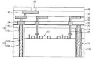
이하에서 설명하는 반도체 소자는 실리콘 관통 비아 콘택의 형상을 제외하고는 도 1에 도시된 반도체 소자와 동일하다. 그러므로, 실리콘 관통 비아 콘택을 주로 설명한다.The semiconductor device described below is the same as the semiconductor device shown in FIG. 1 except for the shape of the through-via via contact. Therefore, silicon through via contacts are mainly described.
도 20을 참조하면, 상기 비아홀(16)의 측벽 및 저면과 상기 제1 층간 절연막(14) 상부면 프로파일을 따라 절연막 구조물(18)이 구비된다. 상기 비아홀(16)의 측벽 및 저면에 위치하는 절연막 구조물(18)은 제1 기판(10)과 비아홀(16) 내의 도전 물질 사이를 절연시키는 역할을 한다. 상기 제1 기판(10)과 비아홀(16) 내의 도전 물질 사이의 기생커패시턴스를 감소시키기 위하여 상기 절연막 구조물(18)은 저유전 물질로 이루어질 수 있다. 상기 절연막 구조물(18)은 실리콘 산화물 또는 탄소 도핑된 실리콘 산화물로 이루어질 수 있으며, 상기 실리콘 산화물은 다공성을 가질 수 있다. 또한, 상기 제1 기판(10)과 비아홀(16) 내의 도전 물질 사이의 기생 커패시턴스를 감소시키기 위하여 상기 절연막 구조물(18)이 두껍게 형성될 수 있다. 상기 절연막 구조물(18)은 1000Å보다 두껍고 상기 비아홀(16) 직경의 1/4의 두께보다는 얇은 두께를 가질 수 있다.Referring to FIG. 20, an insulating
상기 비아홀(16) 측벽 및 저면에 위치하는 절연막 구조물(18) 상에는 배리어 막 패턴(60)이 구비된다. 상기 배리어 막 패턴(60)은 Ta, TaN, Ti, TiN, Ru, Co, Ni, NiB, WN 등의 물질로 형성할 수 있다. 이들은 단독으로 사용되거나 또는 2 이상을 적층하여 사용할 수 있다.The
상기 배리어 막 패턴(60) 상에는 상기 비아홀(16)의 측벽 및 저면을 따라 도전 패턴(62)이 구비된다. 상기 도전 패턴(62)은 저저항을 갖는 금속으로 이루어질 수 있다. 일 예로, 상기 도전 패턴(62)은 구리(Cu)로 이루어질 수 있다. 즉, 상기 도전 패턴(62)은 컵 형상을 갖는다. 상기 도전 패턴(62)은 실질적으로 전기적 신호 전달을 하는 콘택의 역할을 한다.A
상기 도전 패턴(62) 상에는 상기 비아홀(16) 내부를 채우는 갭필 패턴(64)이 구비된다. 상기 갭필 패턴(64)은 절연물질 또는 도전 물질로 이루어질 수 있다. 일 예로, 상기 갭필 패턴(64)은 스핀온 글래스(SOG) 계열의 산화물, 플로우어블 실리콘(Flowable Si), 티타늄, 알루미늄, 다공성 물질(porous material) 등을 들 수 있다.The
상기 실리콘 관통 비아 콘택(66)의 상부면은 상기 제1 층간 절연막 (14)상에 위치하는 제2 절연막(18b)의 상부면과 동일한 평면에 위치한다.An upper surface of the through silicon via
상기 실리콘 관통 비아 콘택(66) 및 절연막 구조물(18) 상부면을 덮는 버퍼막(26)이 구비된다. 상기 버퍼막(26)은 실리콘 질화물, 실리콘 탄소 질화물 및 SiCON 등으로 이루어질 수 있으며, 이들은 단독 또는 2 이상이 적층된 형상을 가질 수 있다.A
상기 절연막 구조물(18) 및 제1 층간 절연막(14)을 관통하여 상기 제1 회로 패턴(12)들과 전기적으로 연결되는 콘택 플러그(28)가 구비된다.A
또한, 도시된 것과 같이 상부 배선들(34, 38) 및 금속간 절연막들(30, 36)이 구비된다.In addition, as illustrated, the
상기 설명한 반도체 소자의 경우에도, 실리콘 관통 비아 콘택와 기판 간의 절연 특성이 우수하고, 기생 커패시턴스가 감소된다. 또한, 반도체 소자에 포함되는 실리콘 관통 비아 콘택은 저저항을 갖고 신호 전달 특성이 우수하다.
Also in the semiconductor device described above, the insulating properties between the silicon through via contact and the substrate are excellent, and the parasitic capacitance is reduced. In addition, the silicon through via contact included in the semiconductor device has low resistance and excellent signal transmission characteristics.
도 21 및 도 22는 도 20에 도시된 반도체 소자를 제조하는 방법을 나타내는 단면도들이다.21 and 22 are cross-sectional views illustrating a method of manufacturing the semiconductor device shown in FIG. 20.
도 2 내지 도 4를 참조로 설명한 것과 동일한 공정을 수행하여, 비아홀(16) 및 절연막 구조물(18)을 형성한다.The via
도 21을 참조하면, 상기 절연막 구조물(18) 상에 배리어 막(61)을 형성한다. 상기 배리어 막(61) 상에 상기 비아홀(16)의 측벽 및 저면 프로파일을 따라 도전막(63)을 형성한다. 상기 도전막(63)은 구리를 포함할 수 있다.Referring to FIG. 21, a
상기 도전막(63) 상에 상기 비아홀(16) 내부를 채우는 갭필용 막(65)을 형성한다. 상기 갭필용 막(65)은 스핀온 글래스(SOG) 계열의 산화물, 플로우어블 실리콘(Flowable Si), 티타늄, 알루미늄, 다공성 물질(porous material) 등을 들 수 있다. 상기 갭필용 막(65)은 상온에서 16.7×10⁻⁶/℃ 이하의 낮은 열팽창계수를 갖거나 열에 의해 부피가 감소되는 물질로 이루어지는 것이 바람직하다. 상기와 같이, 비아홀(16) 내부에 갭필용 막(65)을 형성함으로써, 상기 도전막(63)의 열팽창에 의한 문제를 감소시킬 수 있다.A
도 22를 참조하면, 상기 절연막 구조물(18)의 상부면이 노출되도록 상기 갭필용 막(65), 도전막(63) 및 배리어 막(61)을 연마한다. 이로써, 상기 비아홀(16) 내에 실리콘 관통 비아 콘택(66)을 형성한다. 상기 실리콘 관통 비아 콘택(66)은 배리어막 패턴(60), 도전 패턴(62) 및 갭필막 패턴(64)을 포함한다.Referring to FIG. 22, the
계속하여, 도 7 내지 도 10을 참조로 설명한 공정을 수행한다. 이로써, 도 20에 도시된 반도체 소자를 제조할 수 있다.
Subsequently, the process described with reference to FIGS. 7 to 10 is performed. Thereby, the semiconductor element shown in FIG. 20 can be manufactured.
도 23은 본 발명의 일 실시예에 따른 적층형 반도체 소자를 나타내는 단면도들이다.23 is a cross-sectional view illustrating a stacked semiconductor device according to an embodiment of the present invention.
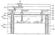
도 23에 도시된 적층형 반도체 소자는 실리콘 관통 비아 콘택의 형상을 제외하고는 도 13에 도시된 적층형 반도체 소자와 동일하다.The stacked semiconductor device shown in FIG. 23 is the same as the stacked semiconductor device shown in FIG. 13 except for the shape of the through silicon via contact.
본 실시예의 절연막 패턴 구조물(19)은 상기 비아홀(16)의 측벽 및 상기 제1 층간 절연막(14) 상에 구비된다. 절연막 패턴 구조물(19)은 제1 절연막 패턴(18c) 및 제2 절연막 패턴(18b)을 포함한다. 그러나, 상기 절연막 패턴 구조물(19)은 상기 비아홀(16)의 저면에는 구비되지 않는다. 즉, 상기 비아홀(16) 측벽에는 상, 하부면이 오픈된 원통 형상의 제1 절연막 패턴(18c)이 구비된다. 상기 제1 절연막 패턴(18c)은 상기 제1 기판(10a)과 실리콘 관통 비아 콘택(66a)간을 절연시키는 역할을 한다. 상기 원통 형상의 제1 절연막 패턴(18c) 상에는 배리어 막 패턴(60a) 및 시드 패턴(도시안함)이 구비된다.The insulating
상기 시드 패턴 상에 상기 비아홀(16) 내부 측벽을 따라 도전 패턴(62a)이 구비된다. 상기 도전 패턴(62a)은 컵 형상을 갖는다. 상기 도전 패턴(62a)의 저면은 상기 제1 기판(10a) 저면에 노출된 형상을 가질 수 있다. 또한, 상기 도전 패턴(62a)의 저면은 상기 제1 기판(10a) 저면과 동일한 평면에 위치하거나 제1 기판(10a) 저면보다 돌출될 수 있다. 상기 도전 패턴(62a)은 구리를 포함할 수 있다.A
또한, 상기 도전 패턴(62a) 상에 상기 비아홀(16) 내부를 채우는 갭필 패턴(64)이 구비된다. 상기 갭필 패턴(64)의 예로는 스핀온 글래스(SOG) 계열의 산화물, 플로우어블 실리콘(Flowable Si), 티타늄, 알루미늄, 다공성 물질(porous material) 등을 들 수 있다.In addition, a
상기한 적층형 반도체 소자는 다음의 공정을 통해 형성할 수 있다.The stacked semiconductor device may be formed through the following process.
먼저, 도 21 및 22를 참조로 설명한 공정을 수행하여 도 20에 도시된 반도체 소자를 형성한다. 이 후, 도 16을 참조로 설명한 공정을 통해 상부 배선들(34, 38, 42) 및 보호막(44)을 형성한다. 계속하여, 도 17 내지 도 19를 참조로 설명한 공정들을 수행함으로써, 도 23에 도시된 적층형 반도체 소자를 완성한다.
First, the semiconductor device illustrated in FIG. 20 is formed by performing the process described with reference to FIGS. 21 and 22. Thereafter, the
이하에서는, 본 발명에 따른 다른 실시예들을 나타낸다.In the following, other embodiments according to the invention are shown.
도 24는 본 발명의 다른 실시예를 도시한 것이다.24 shows another embodiment of the present invention.
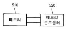
도시된 것과 같이, 본 실시예는 메모리 콘트롤러(520)와 연결된 메모리(510)를 포함한다. 상기 메모리(510)는 상기 본 발명의 각 실시예들에 따른 구조의 적층형 메모리 소자를 포함한다. 상기 메모리 콘트롤러(520)는 상기 메모리의 동작을 콘트롤하기 위한 입력 신호를 제공한다.As shown, the present embodiment includes a
도 25는 또 다른 실시예를 도시한 것이다.25 shows another embodiment.
본 실시예는 호스트 시스템(700)에 연결된 메모리(510)를 포함한다. 상기 메모리(510)는 본 발명의 각 실시예들에 따른 구조의 적층형 메모리 소자를 포함한다.This embodiment includes a
상기 호스트 시스템(700)은 퍼스널 컴퓨터, 카메라, 모바일 기기, 게임기, 통신기기 등과 같은 전자제품을 포함한다. 상기 호스트 시스템(700)은 메모리(510)를 조절하고 작동시키기 위한 입력 신호를 인가하고, 상기 메모리(510)는 데이터 저장 매체로 사용된다.The
도 26은 또 다른 실시예를 도시한 것이다. 본 실시예는 휴대용 장치(600)를 나타낸다. 휴대용 장치(600)는 MP3 플레이어, 비디오 플레이어, 비디오와 오디오 플레이어의 복합기 등일 수 있다. 도시된 것과 같이, 휴대용 장치(600)는 메모리(510) 및 메모리 콘트롤러(520)를 포함한다. 상기 메모리(510)는 본 발명의 각 실시예들에 따른 구조를 갖는 적층형 메모리 소자를 포함한다. 상기 휴대용 장치(600)는 또한 인코더/디코더(610), 표시 부재(620) 및 인터페이스(670)를 포함할 수 있다. 데이터(오디오, 비디오 등)는 인코더/디코더(610)에 의해 상기 메모리 콘트롤러(520)를 경유하여 상기 메모리(510)로부터 입 출력된다.26 shows yet another embodiment. This embodiment shows a
상기 설명한 것과 같이, 본 발명에 의하면 실리콘 관통 비아 콘택을 포함하는 반도체 소자를 제조할 수 있다. 상기 반도체 소자는 용이하게 수직 적층이 가능하므로 고용량이 요구되는 다양한 메모리 소자로써 이용할 수 있다. 특히, 고성능 및 고신뢰성을 갖는 메모리 소자로 이용될 수 있다.As described above, according to the present invention, a semiconductor device including a silicon through via contact can be manufactured. Since the semiconductor device can be easily stacked vertically, it can be used as various memory devices requiring a high capacity. In particular, it can be used as a memory device having high performance and high reliability.
10 : 제1 기판12 : 제1 회로 패턴
14 : 제1 층간 절연막16 : 비아홀
18 : 절연막 구조물18a : 제1 절연막
18b : 제2 절연막, 제2 절연막 패턴18c : 제1 절연막 패턴
20a : 배리어 막 패턴22a : 도전 패턴
24 : 실리콘 관통 비아 콘택26 : 버퍼막
28 : 콘택 플러그30 : 제1 금속간 절연막
34 : 제1 배선36 : 제2 금속간 절연막
38 : 제2 배선44 : 제1 보호막
46 : 제4 개구48 : 솔더
54 : 예비 관통 비아 콘택
50b : 배리어 막 패턴 52a : 도전 패턴
100 : 제2 기판102 : 제2 회로 패턴들
104: 배선들106 : 제2 층간 절연막들
108 : 제2 패드 전극110 : 제2 보호막
112 : 접촉 패턴60, 60a : 배리어 막 패턴
62, 62a : 도전 패턴64 : 갭필 패턴
66, 66a : 실리콘 관통 비아 콘택10: first substrate 12: first circuit pattern
14 first
18: insulating
18b: second insulating film and second
20a:
24: silicon through via contact 26: buffer film
28
34: first wiring 36: second intermetallic insulating film
38: second wiring 44: first protective film
46: fourth opening 48: solder
54: Pre-Through Via Contact
50b:
100: second substrate 102: second circuit patterns
104: wirings 106: second interlayer insulating films
108: second pad electrode 110: second protective film
112:
62, 62a: conductive pattern 64: gap fill pattern
66, 66a: silicon through via contact
Claims (31)
Translated fromKorean상기 회로 패턴들을 덮고, 상부면으로부터 기판 내부까지 관통하는 관통홀을 포함하는 층간 절연막;
상기 관통홀의 측벽, 저면 및 층간 절연막 상부면을 따라 연속적으로 형성된 절연막 구조물;
상기 관통홀 내부에 구비되고, 상기 층간 절연막 상의 절연막 구조물의 상부면과 동일한 상부면 높이를 갖는 실리콘 관통 비아 콘택;
상기 실리콘 관통 비아 콘택 및 절연막 구조물 상부면을 덮는 버퍼막; 및
상기 버퍼막, 절연막 구조물 및 층간 절연막을 관통하여 상기 회로 패턴들과 연결되는 콘택 플러그를 포함하는 반도체 소자.Circuit patterns formed on the substrate;
An interlayer insulating layer covering the circuit patterns and including a through hole penetrating from an upper surface to an inside of the substrate;
An insulating film structure formed continuously along the sidewalls, the bottom surface and the upper surface of the interlayer insulating film of the through hole;
A silicon through via contact provided in the through hole and having a same upper surface height as an upper surface of the insulating film structure on the interlayer insulating film;
A buffer layer covering the silicon through via contact and an upper surface of the insulating layer structure; And
And a contact plug penetrating the buffer layer, the insulating layer structure, and the interlayer insulating layer to connect the circuit patterns.
상기 관통홀의 측벽 및 저면을 따라 증착된 컵 형상 도전 패턴 및
상기 도전 패턴 내부를 채우는 갭필 패턴을 포함하는 형상을 갖는 반도체 소자.The method of claim 1, wherein the through silicon via contact,
A cup-shaped conductive pattern deposited along sidewalls and bottom surfaces of the through holes;
A semiconductor device having a shape including a gap fill pattern filling the inside of the conductive pattern.
상기 회로 패턴들을 덮고, 상부면으로부터 기판 내부까지 관통하는 관통홀을 포함하는 층간 절연막을 형성하는 단계;
상기 관통홀의 측벽, 저면 및 층간 절연막 상부면을 따라 연속적으로 절연막 구조물을 형성하는 단계;
상기 관통홀 내부를 채우면서, 상기 층간 절연막 상의 절연막 구조물의 상부면과 동일한 상부면 높이를 갖는 실리콘 관통 비아 콘택을 형성하는 단계;
상기 실리콘 관통 비아 콘택 및 절연막 구조물 상부면을 덮는 버퍼막을 형성하는 단계; 및
상기 버퍼막, 절연막 구조물 및 층간 절연막을 관통하여 상기 회로 패턴들과 연결되는 콘택 플러그를 형성하는 단계를 포함하는 반도체 소자의 제조 방법.Forming circuit patterns on the substrate;
Forming an interlayer insulating layer covering the circuit patterns and including a through hole penetrating from an upper surface to an inside of a substrate;
Continuously forming an insulating film structure along the sidewalls, the bottom surface and the upper surface of the interlayer insulating film of the through hole;
Filling a through hole and forming a silicon through via contact having a same upper surface height as an upper surface of an insulating film structure on the interlayer insulating film;
Forming a buffer layer covering the silicon through via contact and an upper surface of the insulating layer structure; And
Forming a contact plug connected to the circuit patterns through the buffer layer, the insulating layer structure, and the interlayer insulating layer.
상기 관통홀 내부의 절연막 구조물 상에 배리어 막을 형성하는 단계;
상기 배리어 막 상에 상기 관통홀을 채우도록 구리막을 형성하는 단계; 및
상기 절연막 구조물의 상부면이 노출되도록 상기 구리막 및 배리어 막을 연마하여 실리콘 관통 비아 콘택을 형성하는 단계를 포함하는 반도체 소자의 제조 방법.The method of claim 12, wherein forming the through silicon via contact comprises:
Forming a barrier film on the insulating film structure in the through hole;
Forming a copper film on the barrier film to fill the through hole; And
Polishing the copper film and the barrier film to expose a top surface of the insulating film structure to form a through-via via contact.
상기 실리콘 관통 비아 콘택의 상부면이 상기 절연막 구조물보다 돌출되도록 상기 실리콘 관통 비아 콘택을 열처리하는 단계; 및
상기 실리콘 관통 비아 콘택 및 절연막 구조물의 상부면이 평탄하도록 상기 돌출된 부위의 실리콘 관통 비아 콘택을 연마하는 단계를 포함하는 반도체 소자의 제조 방법.The method of claim 13,
Heat-treating the through silicon via contact such that an upper surface of the through silicon via contact protrudes from the insulating layer structure; And
Polishing the silicon through via contact of the protruding portion so that the silicon through via contact and the top surface of the insulating film structure are flat.
상기 관통홀 내부의 절연막 구조물 상에 배리어 막을 형성하는 단계;
상기 배리어 막 상에 상기 관통홀 측벽 및 저면을 따라 구리막을 형성하는 단계;
상기 구리막 상에 상기 관통홀을 채우는 갭필용 막을 형성하는 단계; 및
상기 절연막 구조물의 상부면이 노출되도록 상기 구리막, 배리어 막 및 갭필용 막을 연마하여 실리콘 관통 비아 콘택을 형성하는 단계를 포함하는 반도체 소자의 제조 방법.The method of claim 12, wherein forming the through silicon via contact comprises:
Forming a barrier film on the insulating film structure in the through hole;
Forming a copper film on the barrier film along sidewalls and bottom surfaces of the through holes;
Forming a gap fill film filling the through hole on the copper film; And
And forming a through-via via contact by polishing the copper film, the barrier film, and the gap-fill film so that the top surface of the insulating film structure is exposed.
상기 버퍼막, 절연막 구조물 및 층간 절연막을 식각하여 콘택홀을 형성하는 단계;
상기 콘택홀 내부에 금속막을 형성하는 단계; 및
상기 버퍼막 표면이 노출되도록 상기 금속막을 연마하여 상기 콘택홀 내부에 콘택 플러그를 형성하는 단계를 포함하는 반도체 소자의 제조 방법.The method of claim 12, wherein the forming of the contact plug comprises:
Etching the buffer layer, the insulating layer structure, and the interlayer insulating layer to form a contact hole;
Forming a metal film in the contact hole; And
And forming a contact plug in the contact hole by polishing the metal film to expose the surface of the buffer film.
상기 관통홀의 측벽 및 저면에 제1 절연막을 형성하는 단계; 및
상기 층간 절연막 상에 제2 절연막을 형성하는 단계를 포함하고,
상기 제1 절연막은 상기 제2 절연막보다 더 두껍게 형성되는 반도체 소자의 제조 방법.The method of claim 12, wherein the forming of the insulating film structure comprises:
Forming a first insulating film on sidewalls and bottom surfaces of the through holes; And
Forming a second insulating film on the interlayer insulating film,
And the first insulating film is formed thicker than the second insulating film.
상기 관통홀의 측벽 및 층간 절연막 상부면에 형성된 절연막 구조물;
상기 관통홀 내부에 구비되고, 상기 층간 절연막 상의 절연막 구조물의 상부면과 동일한 상부면 높이를 갖고, 하부면이 상기 기판 저면에 노출되는 실리콘 관통 비아 콘택;
상기 실리콘 관통 비아 콘택 및 절연막 구조물 상부면을 덮는 버퍼막;
상기 버퍼막, 절연막 구조물 및 층간 절연막을 관통하여 상기 제1 회로 패턴들과 연결되는 콘택 플러그;
상기 콘택 플러그 및 상기 실리콘 관통 비아 콘택 상부면과 전기적으로 연결되는 배선 구조물;
제2 회로 패턴들 및 패드 전극들이 포함되는 제2 기판; 및
상기 제2 기판의 패드 전극들과 실리콘 관통 비아 콘택의 저면을 전기적으로 접촉시키는 접촉 패턴을 포함하는 반도체 소자.An interlayer insulating layer covering the first circuit patterns formed on the first substrate and including a through hole penetrating the substrate from an upper surface thereof;
An insulating film structure formed on the sidewall of the through hole and an upper surface of the interlayer insulating film;
A silicon through via contact provided in the through hole and having a same upper surface height as an upper surface of an insulating film structure on the interlayer insulating layer, and having a lower surface exposed to a bottom surface of the substrate;
A buffer layer covering the silicon through via contact and an upper surface of the insulating layer structure;
A contact plug penetrating the buffer layer, the insulating layer structure, and the interlayer insulating layer to be connected to the first circuit patterns;
A wiring structure electrically connected to the contact plug and the silicon through via contact upper surface;
A second substrate including second circuit patterns and pad electrodes; And
And a contact pattern for electrically contacting pad electrodes of the second substrate and a bottom surface of a silicon through via contact.
상기 관통홀의 측벽 및 층간 절연막 상부면에 절연막 구조물을 형성하는 단계;
상기 관통홀 내부에 구비되고, 상기 층간 절연막 상의 절연막 구조물의 상부면과 동일한 상부면 높이를 갖고, 하부면이 상기 기판 저면에 노출되는 실리콘 관통 비아 콘택을 형성하는 단계;
상기 실리콘 관통 비아 콘택 및 절연막 구조물 상부면을 덮는 버퍼막을 형성하는 단계;
상기 버퍼막, 절연막 구조물 및 층간 절연막을 관통하여 상기 제1 회로 패턴들과 연결되는 콘택 플러그를 형성하는 단계;
상기 콘택 플러그 및 상기 실리콘 관통 비아 콘택 상부면과 전기적으로 연결되는 배선 구조물을 형성하는 단계;
제2 기판에 제2 회로 패턴들 및 패드 전극들을 형성하는 단계; 및
상기 제2 기판의 패드 전극들과 실리콘 관통 비아 콘택의 저면을 전기적으로 접촉시키는 접촉 패턴을 형성하는 단계를 포함하는 반도체 소자 의 제조 방법.Forming an interlayer insulating layer covering the first circuit patterns formed on the first substrate and including a through hole penetrating the substrate from an upper surface thereof;
Forming an insulating film structure on the sidewall of the through hole and an upper surface of the interlayer insulating film;
Forming a silicon through via contact provided in the through hole, the upper surface having the same upper surface as the upper surface of the insulating film structure on the interlayer insulating layer, and having a lower surface exposed to the bottom surface of the substrate;
Forming a buffer layer covering the silicon through via contact and an upper surface of the insulating layer structure;
Forming a contact plug penetrating the buffer layer, the insulating layer structure, and the interlayer insulating layer to be connected to the first circuit patterns;
Forming a wiring structure electrically connected to the contact plug and the silicon through via contact top surface;
Forming second circuit patterns and pad electrodes on a second substrate; And
And forming a contact pattern for electrically contacting pad electrodes of the second substrate and a bottom surface of the silicon through via contact.
Priority Applications (4)
| Application Number | Priority Date | Filing Date | Title |
|---|---|---|---|
| KR1020100061184AKR20120000748A (en) | 2010-06-28 | 2010-06-28 | Semiconductor device and manufacturing method thereof |
| US12/913,753US8076234B1 (en) | 2010-06-28 | 2010-10-27 | Semiconductor device and method of fabricating the same including a conductive structure is formed through at least one dielectric layer after forming a via structure |
| US13/287,317US8847399B2 (en) | 2010-06-28 | 2011-11-02 | Semiconductor device and method of fabricating the same |
| US13/627,790US9018768B2 (en) | 2010-06-28 | 2012-09-26 | Integrated circuit having through silicon via structure with minimized deterioration |
Applications Claiming Priority (1)
| Application Number | Priority Date | Filing Date | Title |
|---|---|---|---|
| KR1020100061184AKR20120000748A (en) | 2010-06-28 | 2010-06-28 | Semiconductor device and manufacturing method thereof |
Publications (1)
| Publication Number | Publication Date |
|---|---|
| KR20120000748Atrue KR20120000748A (en) | 2012-01-04 |
Family
ID=45092653
Family Applications (1)
| Application Number | Title | Priority Date | Filing Date |
|---|---|---|---|
| KR1020100061184AWithdrawnKR20120000748A (en) | 2010-06-28 | 2010-06-28 | Semiconductor device and manufacturing method thereof |
Country Status (2)
| Country | Link |
|---|---|
| US (2) | US8076234B1 (en) |
| KR (1) | KR20120000748A (en) |
Cited By (3)
| Publication number | Priority date | Publication date | Assignee | Title |
|---|---|---|---|---|
| KR101412828B1 (en)* | 2012-04-27 | 2014-06-27 | 타이완 세미콘덕터 매뉴팩쳐링 컴퍼니 리미티드 | Through-substrate vias and methods for forming same |
| KR20150091714A (en)* | 2014-02-03 | 2015-08-12 | 삼성전자주식회사 | Via Structures and Semiconductor Devices Having a Via plug |
| US9123702B2 (en) | 2012-08-10 | 2015-09-01 | Taiwan Semiconductor Manufacturing Company, Ltd. | Connecting through vias to devices |
Families Citing this family (39)
| Publication number | Priority date | Publication date | Assignee | Title |
|---|---|---|---|---|
| KR101374338B1 (en)* | 2007-11-14 | 2014-03-14 | 삼성전자주식회사 | semicondoctor device having through-via and method of forming the same |
| JP2009147218A (en)* | 2007-12-17 | 2009-07-02 | Toshiba Corp | Semiconductor device and manufacturing method thereof |
| US9293366B2 (en)* | 2010-04-28 | 2016-03-22 | Taiwan Semiconductor Manufacturing Company, Ltd. | Through-substrate vias with improved connections |
| KR20120030782A (en)* | 2010-09-20 | 2012-03-29 | 삼성전자주식회사 | Method of forming through silicon via using low-k material |
| JP2012195514A (en)* | 2011-03-17 | 2012-10-11 | Seiko Epson Corp | Substrate with element, infrared sensor, and through electrode formation method |
| US9305865B2 (en)* | 2013-10-31 | 2016-04-05 | Micron Technology, Inc. | Devices, systems and methods for manufacturing through-substrate vias and front-side structures |
| JP5733002B2 (en)* | 2011-04-28 | 2015-06-10 | 富士通セミコンダクター株式会社 | Manufacturing method of semiconductor device |
| US8587127B2 (en)* | 2011-06-15 | 2013-11-19 | Taiwan Semiconductor Manufacturing Company, Ltd. | Semiconductor structures and methods of forming the same |
| US8822336B2 (en)* | 2011-06-16 | 2014-09-02 | United Microelectronics Corp. | Through-silicon via forming method |
| FR2978296A1 (en)* | 2011-07-20 | 2013-01-25 | St Microelectronics Crolles 2 | ELECTRONIC CHIP COMPRISING CONNECTION PILLARS, AND METHOD OF MANUFACTURE |
| US8803322B2 (en)* | 2011-10-13 | 2014-08-12 | Taiwan Semiconductor Manufacturing Company, Ltd. | Through substrate via structures and methods of forming the same |
| US20130270712A1 (en)* | 2012-04-16 | 2013-10-17 | Hsin-Yu Chen | Through silicon via structure and method of fabricating the same |
| US8587131B1 (en)* | 2012-06-07 | 2013-11-19 | Nanya Technology Corp. | Through-silicon via and fabrication method thereof |
| US8956974B2 (en)* | 2012-06-29 | 2015-02-17 | Micron Technology, Inc. | Devices, systems, and methods related to planarizing semiconductor devices after forming openings |
| US8963336B2 (en) | 2012-08-03 | 2015-02-24 | Samsung Electronics Co., Ltd. | Semiconductor packages, methods of manufacturing the same, and semiconductor package structures including the same |
| KR101932660B1 (en) | 2012-09-12 | 2018-12-26 | 삼성전자 주식회사 | Integrated circuit device having through silicon via structure and method of manufacturing the same |
| KR20140073163A (en) | 2012-12-06 | 2014-06-16 | 삼성전자주식회사 | Semiconductor device and method of forming the same |
| US9764153B2 (en) | 2013-03-14 | 2017-09-19 | Taiwan Semiconductor Manufacturing Company, Ltd. | Interconnect structure and method of forming same |
| KR20150013980A (en)* | 2013-07-24 | 2015-02-06 | 삼성전자주식회사 | Method of manufacturing semiconductor device |
| US20150069609A1 (en)* | 2013-09-12 | 2015-03-12 | International Business Machines Corporation | 3d chip crackstop |
| US9093503B1 (en)* | 2014-01-03 | 2015-07-28 | International Business Machines Corporation | Semiconductor chip with a dual damascene wire and through-substrate via (TSV) structure |
| US10170396B2 (en)* | 2014-02-14 | 2019-01-01 | Taiwan Semiconductor Manufacturing Company, Ltd. | Through via structure extending to metallization layer |
| US9583417B2 (en)* | 2014-03-12 | 2017-02-28 | Invensas Corporation | Via structure for signal equalization |
| KR102299781B1 (en) | 2014-07-21 | 2021-09-08 | 삼성전자주식회사 | Semiconductor devices and methods of manufacturing the same |
| US9978607B2 (en)* | 2014-09-05 | 2018-05-22 | Taiwan Semiconductor Manufacturing Company, Ltd. | Through via structure and method |
| US9807867B2 (en) | 2016-02-04 | 2017-10-31 | Taiwan Semiconductor Manufacturing Co., Ltd. | Interconnect structure and method of manufacturing the same |
| KR102497205B1 (en) | 2016-03-03 | 2023-02-09 | 삼성전자주식회사 | Semiconductor devices having through electrodes and methods for fabricating the same |
| US10049981B2 (en)* | 2016-09-08 | 2018-08-14 | Taiwan Semiconductor Manufacturing Company Ltd. | Through via structure, semiconductor device and manufacturing method thereof |
| JP2018157110A (en)* | 2017-03-17 | 2018-10-04 | 東芝メモリ株式会社 | Semiconductor device and manufacturing method thereof |
| DE202019006156U1 (en) | 2018-11-30 | 2025-06-12 | Taiwan Semiconductor Manufacturing Company, Ltd. | Functional component within an interconnect structure of a semiconductor device |
| US11183454B2 (en) | 2018-11-30 | 2021-11-23 | Taiwan Semiconductor Manufacturing Company, Ltd. | Functional component within interconnect structure of semiconductor device and method of forming same |
| KR102815080B1 (en) | 2019-08-07 | 2025-05-30 | 삼성전자주식회사 | Vertical semiconductor devices |
| KR102737514B1 (en)* | 2020-06-11 | 2024-12-05 | 삼성전자주식회사 | Semiconductor devices and method of manufacturing the same |
| US11823989B2 (en)* | 2020-07-17 | 2023-11-21 | Taiwan Semiconductor Manufacturing Co., Ltd. | Multi-liner TSV structure and method forming same |
| CN111968955B (en)* | 2020-08-27 | 2021-10-12 | 武汉新芯集成电路制造有限公司 | Semiconductor device and method for manufacturing the same |
| CN117936507A (en)* | 2020-09-02 | 2024-04-26 | 长江存储科技有限责任公司 | Pad lead-out structure for Xtacking architecture |
| KR102824470B1 (en)* | 2021-02-23 | 2025-06-26 | 삼성전자주식회사 | Semiconductor device and stacked semiconductor chips |
| CN116072547B (en)* | 2021-10-29 | 2025-10-03 | 长鑫存储技术有限公司 | Semiconductor structure and forming method thereof, and wafer bonding method |
| US12322654B2 (en)* | 2021-10-29 | 2025-06-03 | Changxin Memory Technologies, Inc. | Semiconductor structure, method for forming same, and wafer on wafer bonding method |
Family Cites Families (18)
| Publication number | Priority date | Publication date | Assignee | Title |
|---|---|---|---|---|
| JP4408006B2 (en) | 2001-06-28 | 2010-02-03 | 富士通マイクロエレクトロニクス株式会社 | Semiconductor device and manufacturing method thereof |
| JP2007317954A (en) | 2006-05-26 | 2007-12-06 | Nec Electronics Corp | Semiconductor device and manufacturing method thereof |
| US7626269B2 (en)* | 2006-07-06 | 2009-12-01 | Micron Technology, Inc. | Semiconductor constructions and assemblies, and electronic systems |
| KR100817718B1 (en) | 2006-12-27 | 2008-03-27 | 동부일렉트로닉스 주식회사 | Semiconductor device manufacturing method |
| KR100906065B1 (en) | 2007-07-12 | 2009-07-03 | 주식회사 동부하이텍 | Semiconductor chip, manufacturing method thereof and laminated package having same |
| KR100896883B1 (en) | 2007-08-16 | 2009-05-14 | 주식회사 동부하이텍 | Semiconductor chip, manufacturing method thereof and laminated package having same |
| KR100929464B1 (en) | 2007-12-21 | 2009-12-02 | 주식회사 동부하이텍 | Semiconductor chip, manufacturing method thereof and semiconductor chip stack package |
| US7799678B2 (en) | 2008-01-30 | 2010-09-21 | Freescale Semiconductor, Inc. | Method for forming a through silicon via layout |
| JP2009277719A (en) | 2008-05-12 | 2009-11-26 | Nec Electronics Corp | Semiconductor device and method of manufacturing the same |
| US8043973B2 (en)* | 2008-05-22 | 2011-10-25 | Texas Instruments Incorporated | Mask overhang reduction or elimination after substrate etch |
| JP2010010324A (en) | 2008-06-26 | 2010-01-14 | Toshiba Corp | Semiconductor device and method of manufacturing the same |
| US20100065949A1 (en)* | 2008-09-17 | 2010-03-18 | Andreas Thies | Stacked Semiconductor Chips with Through Substrate Vias |
| US7855455B2 (en)* | 2008-09-26 | 2010-12-21 | International Business Machines Corporation | Lock and key through-via method for wafer level 3 D integration and structures produced |
| US8252659B2 (en)* | 2008-12-02 | 2012-08-28 | Imec | Method for producing interconnect structures for integrated circuits |
| US7816945B2 (en)* | 2009-01-22 | 2010-10-19 | International Business Machines Corporation | 3D chip-stack with fuse-type through silicon via |
| US8168529B2 (en)* | 2009-01-26 | 2012-05-01 | Taiwan Semiconductor Manufacturing Company, Ltd. | Forming seal ring in an integrated circuit die |
| US7960282B2 (en)* | 2009-05-21 | 2011-06-14 | Globalfoundries Singapore Pte. Ltd. | Method of manufacture an integrated circuit system with through silicon via |
| US8487425B2 (en)* | 2011-06-23 | 2013-07-16 | International Business Machines Corporation | Optimized annular copper TSV |
- 2010
- 2010-06-28KRKR1020100061184Apatent/KR20120000748A/ennot_activeWithdrawn
- 2010-10-27USUS12/913,753patent/US8076234B1/enactiveActive
- 2011
- 2011-11-02USUS13/287,317patent/US8847399B2/enactiveActive
Cited By (4)
| Publication number | Priority date | Publication date | Assignee | Title |
|---|---|---|---|---|
| KR101412828B1 (en)* | 2012-04-27 | 2014-06-27 | 타이완 세미콘덕터 매뉴팩쳐링 컴퍼니 리미티드 | Through-substrate vias and methods for forming same |
| US9123702B2 (en) | 2012-08-10 | 2015-09-01 | Taiwan Semiconductor Manufacturing Company, Ltd. | Connecting through vias to devices |
| US9355935B2 (en) | 2012-08-10 | 2016-05-31 | Taiwan Semiconductor Manufactruing Company, Ltd. | Connecting through vias to devices |
| KR20150091714A (en)* | 2014-02-03 | 2015-08-12 | 삼성전자주식회사 | Via Structures and Semiconductor Devices Having a Via plug |
Also Published As
| Publication number | Publication date |
|---|---|
| US20110318923A1 (en) | 2011-12-29 |
| US8076234B1 (en) | 2011-12-13 |
| US20120043666A1 (en) | 2012-02-23 |
| US8847399B2 (en) | 2014-09-30 |
Similar Documents
| Publication | Publication Date | Title |
|---|---|---|
| KR20120000748A (en) | Semiconductor device and manufacturing method thereof | |
| KR101692434B1 (en) | Semiconductor device and method of manufacturing the same | |
| KR101677507B1 (en) | Method of manufacturing semiconductor devices | |
| JP5916077B2 (en) | Manufacturing method of semiconductor device | |
| US8872354B2 (en) | Method of forming through silicon via of semiconductor device using low-K dielectric material | |
| KR102111474B1 (en) | Semiconductor devices having through electrodes and methods for fabricating the same | |
| KR100889553B1 (en) | System in package and method for fabricating the same | |
| US11488860B2 (en) | Integrated circuit device and method of manufacturing the same | |
| US11069597B2 (en) | Semiconductor chips and methods of manufacturing the same | |
| US20130119547A1 (en) | Integrated circuit device including through-silicon via structure having offset interface | |
| KR20110050957A (en) | Through-via contact of semiconductor device and forming method | |
| KR20120090417A (en) | Semiconductor device and method of manufacturing a semiconductor device | |
| CN101924096A (en) | Through-silicon via structure and its formation process | |
| JP2010045371A (en) | Through-silicon-via structure including conductive protective film, and method of forming the same | |
| JP2015079960A (en) | Integrated circuit element and method for manufacturing the same | |
| CN101197298A (en) | Manufacturing method of semiconductor device and semiconductor device | |
| KR20120067525A (en) | Semiconductor device and method of manufacturing the same | |
| KR102497205B1 (en) | Semiconductor devices having through electrodes and methods for fabricating the same | |
| KR102110247B1 (en) | Semiconductor devices having through electrodes and methods for fabricating the same | |
| KR100777926B1 (en) | Semiconductor device and manufacturing method | |
| TWI571988B (en) | Chip with through silicon via electrode and method of forming the same | |
| KR20150019089A (en) | Semiconductor devices having through vias and methods for fabricating the same | |
| US20250118662A1 (en) | Semiconductor device including a through via and a wiring layer | |
| US20240071923A1 (en) | Semiconductor device |
Legal Events
| Date | Code | Title | Description |
|---|---|---|---|
| PA0109 | Patent application | Patent event code:PA01091R01D Comment text:Patent Application Patent event date:20100628 | |
| PG1501 | Laying open of application | ||
| PC1203 | Withdrawal of no request for examination | ||
| WITN | Application deemed withdrawn, e.g. because no request for examination was filed or no examination fee was paid |