KR20110136532A - 1T DRAM device having two gates in the recessed body, its operation method and manufacturing method - Google Patents
1T DRAM device having two gates in the recessed body, its operation method and manufacturing methodDownload PDFInfo
- Publication number
- KR20110136532A KR20110136532AKR1020100056615AKR20100056615AKR20110136532AKR 20110136532 AKR20110136532 AKR 20110136532AKR 1020100056615 AKR1020100056615 AKR 1020100056615AKR 20100056615 AKR20100056615 AKR 20100056615AKR 20110136532 AKR20110136532 AKR 20110136532A
- Authority
- KR
- South Korea
- Prior art keywords
- gate
- gates
- dram device
- insulating film
- recessed
- Prior art date
- Legal status (The legal status is an assumption and is not a legal conclusion. Google has not performed a legal analysis and makes no representation as to the accuracy of the status listed.)
- Granted
Links
Images


Classifications
- H—ELECTRICITY
- H10—SEMICONDUCTOR DEVICES; ELECTRIC SOLID-STATE DEVICES NOT OTHERWISE PROVIDED FOR
- H10D—INORGANIC ELECTRIC SEMICONDUCTOR DEVICES
- H10D84/00—Integrated devices formed in or on semiconductor substrates that comprise only semiconducting layers, e.g. on Si wafers or on GaAs-on-Si wafers
- H10D84/01—Manufacture or treatment
- H10D84/0123—Integrating together multiple components covered by H10D12/00 or H10D30/00, e.g. integrating multiple IGBTs
- H10D84/0126—Integrating together multiple components covered by H10D12/00 or H10D30/00, e.g. integrating multiple IGBTs the components including insulated gates, e.g. IGFETs
- H10D84/0135—Manufacturing their gate conductors
- H10D84/014—Manufacturing their gate conductors the gate conductors having different materials or different implants
- H—ELECTRICITY
- H01—ELECTRIC ELEMENTS
- H01L—SEMICONDUCTOR DEVICES NOT COVERED BY CLASS H10
- H01L21/00—Processes or apparatus adapted for the manufacture or treatment of semiconductor or solid state devices or of parts thereof
- H01L21/70—Manufacture or treatment of devices consisting of a plurality of solid state components formed in or on a common substrate or of parts thereof; Manufacture of integrated circuit devices or of parts thereof
- H01L21/71—Manufacture of specific parts of devices defined in group H01L21/70
- H01L21/76—Making of isolation regions between components
- H01L21/762—Dielectric regions, e.g. EPIC dielectric isolation, LOCOS; Trench refilling techniques, SOI technology, use of channel stoppers
- H01L21/7624—Dielectric regions, e.g. EPIC dielectric isolation, LOCOS; Trench refilling techniques, SOI technology, use of channel stoppers using semiconductor on insulator [SOI] technology
- H—ELECTRICITY
- H10—SEMICONDUCTOR DEVICES; ELECTRIC SOLID-STATE DEVICES NOT OTHERWISE PROVIDED FOR
- H10B—ELECTRONIC MEMORY DEVICES
- H10B12/00—Dynamic random access memory [DRAM] devices
- H10B12/30—DRAM devices comprising one-transistor - one-capacitor [1T-1C] memory cells
- H10B12/31—DRAM devices comprising one-transistor - one-capacitor [1T-1C] memory cells having a storage electrode stacked over the transistor
- H10B12/318—DRAM devices comprising one-transistor - one-capacitor [1T-1C] memory cells having a storage electrode stacked over the transistor the storage electrode having multiple segments
- H—ELECTRICITY
- H10—SEMICONDUCTOR DEVICES; ELECTRIC SOLID-STATE DEVICES NOT OTHERWISE PROVIDED FOR
- H10B—ELECTRONIC MEMORY DEVICES
- H10B12/00—Dynamic random access memory [DRAM] devices
- H10B12/30—DRAM devices comprising one-transistor - one-capacitor [1T-1C] memory cells
- H10B12/37—DRAM devices comprising one-transistor - one-capacitor [1T-1C] memory cells the capacitor being at least partially in a trench in the substrate
- H10B12/377—DRAM devices comprising one-transistor - one-capacitor [1T-1C] memory cells the capacitor being at least partially in a trench in the substrate having a storage electrode extension located over the transistor
Landscapes
- Engineering & Computer Science (AREA)
- Physics & Mathematics (AREA)
- Condensed Matter Physics & Semiconductors (AREA)
- General Physics & Mathematics (AREA)
- Manufacturing & Machinery (AREA)
- Computer Hardware Design (AREA)
- Microelectronics & Electronic Packaging (AREA)
- Power Engineering (AREA)
- Semiconductor Memories (AREA)
Abstract
Translated fromKoreanDescription
Translated fromKorean본 발명은 반도체 메모리 소자와 그 동작방법 및 제조방법에 관한 것으로, 더욱 상세하게는 커패시터 없이 함몰된 바디에 두개의 게이트로 하나의 트랜지스터 구조를 갖는 1T 디램 소자와 그 동작방법 및 제조방법에 관한 것이다.BACKGROUND OF THE
종래 디램 소자(DRAM device 또는 DRAM memory cell)는 1개의 트랜지스터와 1개의 커패시터로 구성된 1T/1C의 구조를 갖게 되는데, 이는 커패시스터 형성 공정이 복잡하고, 메모리 칩을 다른 소자들과 함께 임베디드(embedded) 칩을 형성하며 고집적화 하는데 한계가 있어 왔다.A conventional DRAM device (DRAM device or DRAM memory cell) has a structure of 1T / 1C composed of one transistor and one capacitor, which is complicated to form a capacitor and embeds a memory chip together with other devices. There is a limit to forming chips and high integration.
그래서, 최근에는 상기 1T/1C 디램 소자의 문제점을 해결하기 위해 커패시터 없이 하나의 트랜지스터 구조를 갖는 1T 디램 소자가 개발되어 왔다(한국 등록특허 10-0860744 및 10-0945508, 한국 공개특허 10-2008-0064001 참조).Thus, in order to solve the problem of the 1T / 1C DRAM device, a 1T DRAM device having a transistor structure without a capacitor has been recently developed (Korean Patent Nos. 10-0860744 and 10-0945508, and Korean Patent Publication No. 10-2008-A). 0064001).
1T 디램 소자에서 "1" 상태는 일반적으로 충돌 이온화(Impact Ionization) 혹은 GIDL(Gate Induced Drain Leakage) 전류로 생성되는 과잉 홀들(excess holes)이 플로팅 바디(floating body)에 축적된 상태로 정의하고, 반대로 축적된 홀들을 바디와 소스/드레인 사이에 순방향 바이어스를 가하여 제거한 상태를 "0" 상태로 정의한다.In the 1T DRAM device, the "1" state is generally defined as a state in which excess holes generated by collision ionization or gate induced drain leakage (GIDL) current are accumulated in the floating body. On the contrary, a state in which the accumulated holes are removed by applying a forward bias between the body and the source / drain is defined as a “0” state.
플로팅 바디에 홀들이 축적될 경우 바디 전위를 증가시키게 되어, 동일한 게이트 전압이라도 바디에 홀들이 축적 되었는지 여부에 따라 트랜지스터의 전류에 차이가 있게 되는데, 이를 이용하여 메모리 셀의 저장 정보를 읽게된다.When holes are accumulated in the floating body, the body potential is increased, and even though the same gate voltage is increased, currents of the transistors differ depending on whether holes are accumulated in the body, and the storage information of the memory cell is read using the holes.
메모리 동작에 있어 소자는 대부분의 시간을 저장된 데이터를 유지하는 hold 상태에 있게 된다. 따라서 hold 상태의 바이어스 조건은 플로팅 바디에 저장된 홀이 소스/드레인 전극으로 빠져 나가는 것을 방지하기 위하여 게이트 단자에 음의 전압을 인가하는 것이 일반적이다.In memory operation, the device is in a hold state that holds the stored data most of the time. Therefore, in the bias condition of the hold state, it is common to apply a negative voltage to the gate terminal to prevent the holes stored in the floating body from escaping to the source / drain electrodes.
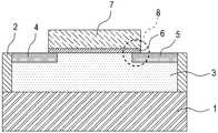
그런데, 도 1과 같이, 게이트(7)와 드레인(5)이 overlap된 구조(8)를 이용하는 1T 디램 소자는 hold 상태에 GIDL 전류가 발생하여 원하지 않는 과잉 홀들(excess holes)이 생성되고, 이로인해 데이터 "0"의 보유시간(retention time)이 줄어들게 되는 문제점이 있다.However, as shown in FIG. 1, in the 1T DRAM device using the
상기와 같은 문제점을 해결하기 위하여 최근에는, 도 2와 같이, 게이트(7a)와 드레인(5a)이 underlap된 형태(8a)를 가지는 여러가지 소자가 제안되었다.In order to solve the above problem, as shown in FIG. 2, various devices having a
그러나, 게이트와 드레인이 underlap된 소자는 GIDL 현상을 이용할 수 없게 되어, 쓰기 동작시 충돌 이온화 현상으로만 과잉 홀들(excess holes)을 생성할 수 밖에 없어 소자의 열화로 인한 신뢰성 문제가 대두되었고, 그 결과 "0"의 보유시간 특성과 신뢰성 특성은 일종의 trade-off로 여겨졌다.However, devices with underlapdated gates and drains cannot use the GIDL phenomenon, and only have to create excess holes due to the collision ionization phenomenon during the write operation, resulting in reliability problems due to deterioration of the device. Results The retention time characteristics and reliability characteristics of "0" were considered a kind of trade-off.
도 1 및 도 2에서 미설명된 도면부호 1은 매몰 산화막, 2는 소자 분리 절연막, 3은 바디(플로팅 바디), 4 및 4a는 소스, 6 및 6a는 게이트 절연막, 9는 절연막 측벽을 각각 가리킨다.In FIG. 1 and FIG. 2,
따라서, 본 발명은 종래 1T 디램 소자의 가장 큰 단점으로 여겨졌던 데이터 "0"의 보유시간 문제와 충돌 이온화로 데이터 "1"을 형성함으로써 발생하는 신뢰성 문제를 동시에 해결할 수 있도록 고안된 함몰된 바디에 두개의 게이트를 갖는 1T 디램 소자의 구조를 제공하는데 그 목적이 있다.Accordingly, the present invention has two recessed bodies designed to solve the problem of retention time of data "0", which was considered as the biggest disadvantage of the conventional 1T DRAM device, and the reliability problem caused by forming data "1" by collision ionization. Its purpose is to provide a structure of a 1T DRAM device having a gate of.
아울러, 본 발명에 따른 함몰된 바디에 두개의 게이트를 갖는 1T 디램 소자의 동작방법 및 제조방법을 제공하는데 다른 목적이 있다.In addition, another object of the present invention is to provide a method of manufacturing and operating a 1T DRAM device having two gates in a recessed body.
상기 목적을 달성하기 위하여, 본 발명에 의한 함몰된 바디에 두개의 게이트를 갖는 1T 디램 소자는 전기적으로 고립되고 함몰된 반도체 바디와; 상기 반도체 바디의 함몰된 부분에 형성된 게이트 절연막과; 상기 게이트 절연막 상에 분리 절연막을 사이에 두고 상기 반도체 바디의 함몰된 부분에 채워진 제 1 및 제 2 게이트를 포함하여 구성된 것을 특징으로 한다.In order to achieve the above object, the 1T DRAM device having two gates in the recessed body according to the present invention comprises an electrically isolated and recessed semiconductor body; A gate insulating film formed on the recessed portion of the semiconductor body; And first and second gates filled in the recessed portion of the semiconductor body with a separation insulating film interposed therebetween on the gate insulating film.
그리고, 상기 제 1 및 제 2 게이트는 상기 반도체 바디의 함몰된 부분에 수직하게 적층되며 밑으로부터 제 2 게이트->제 1 게이트 순으로 채워지고, 상기 제 1 게이트 양측의 상기 반도체 바디 상에 상기 제 1 게이트의 상부 일측과 일부 겹치며 소스 및 드레인이 형성된 것을 본 발명에 의한 함몰된 바디에 두개의 게이트를 갖는 1T 디램 소자의 다른 특징으로 한다.The first and second gates are vertically stacked on the recessed portion of the semiconductor body, and are filled in the order of the second gate to the first gate from below, and the first and second gates are disposed on the semiconductor body on both sides of the first gate. Another feature of the 1T DRAM device having two gates in the recessed body according to the present invention is that the source and the drain are partially overlapped with one upper side of the first gate.
그리고, 상기 반도체 바디는 하측으로 매몰산화막, 측면으로 격리절연막 또는 보이드(void)로 이웃 소자와 전기적으로 고립된 것을 본 발명에 의한 함몰된 바디에 두개의 게이트를 갖는 1T 디램 소자의 또 다른 특징으로 한다.The semiconductor body is electrically isolated from a neighboring device with a buried oxide film on the lower side, an insulating insulating film or a void on the side, and is another feature of the 1T DRAM device having two gates in the recessed body according to the present invention. do.
그리고, 상기 반도체 바디의 함몰된 부분은 상기 매몰산화막 상에 반도체 바디가 존재하도록 트렌치 형태로 형성된 것을 본 발명에 의한 함몰된 바디에 두개의 게이트를 갖는 1T 디램 소자의 또 다른 특징으로 한다.In addition, the recessed portion of the semiconductor body is formed as a trench so that the semiconductor body is present on the buried oxide film, which is another feature of the 1T DRAM device having two gates in the recessed body according to the present invention.
한편, 본 발명에 의한 함몰된 바디에 두개의 게이트를 갖는 1T 디램 소자의 동작방법은 상기 제 1 게이트 및 상기 제 2 게이트에 각각 음의 전압을 인가하고, 상기 소스는 접지, 상기 드레인은 양의 전압을 인가하여 쓰기 동작을 하는 것을 특징으로 한다.On the other hand, in the method of operating a 1T DRAM device having two gates in the recessed body according to the present invention, a negative voltage is applied to the first gate and the second gate, respectively, the source is ground and the drain is positive. A write operation is performed by applying a voltage.
그리고, 상기 제 1 게이트에 인가된 음의 전압이 상기 제 2 게이트에 인가된 음의 전압보다 절대값이 더 큰 것을 본 발명에 의한 함몰된 바디에 두개의 게이트를 갖는 1T 디램 소자 동작방법의 다른 특징으로 한다.In addition, another method of operating a 1T DRAM device having two gates in a recessed body according to the present invention, in which a negative voltage applied to the first gate is greater in absolute value than a negative voltage applied to the second gate. It features.
그리고, 상기 제 1 게이트는 접지시키고, 상기 제 2 게이트는 음의 전압을 인가하여 홀드(hold) 동작을 하는 것을 본 발명에 의한 함몰된 바디에 두개의 게이트를 갖는 1T 디램 소자 동작방법의 또 다른 특징으로 한다.Another method of operating a 1T DRAM device having two gates in a recessed body according to the present invention, wherein the first gate is grounded and the second gate is applied with a negative voltage to perform a hold operation. It features.
한편, 본 발명에 의한 함몰된 바디에 두개의 게이트를 갖는 1T 디램 소자의 제조방법은 SOI 기판에 액티브 영역을 정의하고, 상기 액티브 영역 상에 식각 마스크를 형성하는 제 1 단계와; 상기 식각 마스크로 상기 SOI 기판의 실리콘을 식각하여 트렌치를 형성하되, 상기 트렌치 바닥에 상기 실리콘이 남아 있도록 하는 제 2 단계와; 상기 트렌치 상에 게이트 절연막을 형성하는 제 3 단계와; 상기 게이트 절연막 상에 제 2 게이트->분리 절연막->제 1 게이트 순으로 적층 형성하며 상기 트렌치를 채우는 제 4 단계를 포함하여 구성된 것을 특징으로 한다.Meanwhile, a method of manufacturing a 1T DRAM device having two gates in a recessed body according to the present invention may include a first step of defining an active region in an SOI substrate and forming an etch mask on the active region; Forming a trench by etching silicon of the SOI substrate with the etching mask, wherein the silicon remains at the bottom of the trench; Forming a gate insulating film on the trench; And forming a stack on the gate insulating film in the order of the second gate-> separation insulating film-> first gate and filling the trench.
그리고, 상기 제 4 단계 이후에 상기 식각 마스크를 제거하고 이온주입 공정으로 소스 및 드레인을 형성하는 제 5 단계를 더 포함하는 것을 본 발명에 의한 함몰된 바디에 두개의 게이트를 갖는 1T 디램 소자 제조방법의 다른 특징으로 한다.After the fourth step, the method further includes a fifth step of removing the etching mask and forming a source and a drain by an ion implantation process. With other features.
그리고, 상기 제 1 게이트 및 상기 제 2 게이트는 불순물이 도핑된 실리콘계 물질로 형성되고, 상기 게이트 절연막 및 상기 분리 절연막 형성은 열 산화공정에 의하고, 상기 분리 절연막을 형성할 때 상기 제 2 게이트 형성시 일부 식각된 상기 게이트 절연막도 다시 형성되는 것을 본 발명에 의한 함몰된 바디에 두개의 게이트를 갖는 1T 디램 소자 제조방법의 또 다른 특징으로 한다.The first gate and the second gate are formed of a silicon-based material doped with an impurity, and the gate insulating film and the isolation insulating film are formed by a thermal oxidation process, and when the second gate is formed when the second insulating film is formed. Another feature of the method of manufacturing a 1T DRAM device having two gates in a recessed body according to the present invention is that the partially etched gate insulating film is formed again.
본 발명은 함몰된 바디에 두개의 게이트를 갖는 구조를 함으로써, GIDL 현상을 이용한 쓰기 동작이 가능하여 종래 소자의 신뢰성 문제를 해결할 수 있음은 물론 드레인과 겹치지 않는 게이트에 음의 전압을 독립적으로 가할 수 있어 데이터 "0"의 보유시간을 획기적으로 늘릴 수 있게 된 효과가 있다.According to the present invention, the structure having two gates in the recessed body enables the write operation using the GIDL phenomenon to solve the reliability problem of the conventional device as well as to independently apply a negative voltage to the gate that does not overlap the drain. As a result, the retention time of the data "0" can be significantly increased.
도 1 및 도 2는 각각 게이트와 드레인이 overlap, underlap된 구조를 보여주는 종래 1T 디램 소자의 단면도이다.
도 3은 본 발명에 의한 함몰된 바디에 두개의 게이트를 갖는 1T 디램 소자의 구조를 일 예시적으로 보여주는 단면도이다.
도 4는 시뮬레이션으로 도 3의 구조를 갖는 1T 디램 소자의 동작특성을 파악하기 위한 일 예로 바이어스 인가 조건을 나타낸 그래프이다.
도 5는 도 4에 따라 시뮬레이션시킨 소자의 드레인 전류를 나타낸 전기적 특성도이다.
도 6은 도 4에 따라 시뮬레이션시킨 소자의 보유시간 특성도이다.
도 7 내지 도 13은 각각 도 3의 구조를 제조하기 위한 제조 공정 사시도이다.1 and 2 are cross-sectional views of a conventional 1T DRAM device showing a structure in which a gate and a drain overlap and underlap, respectively.
3 is a cross-sectional view illustrating a structure of a 1T DRAM device having two gates in a recessed body according to the present invention.
FIG. 4 is a graph illustrating bias application conditions as an example for determining an operating characteristic of a 1T DRAM device having the structure of FIG. 3 by simulation.
5 is an electrical characteristic diagram illustrating a drain current of a device simulated according to FIG. 4.
6 is a retention time characteristic diagram of a device simulated according to FIG. 4.
7 to 13 are perspective views illustrating a manufacturing process for manufacturing the structure of FIG. 3, respectively.
이하, 첨부된 도면을 참조하며 본 발명의 각 모습에 따른 바람직한 실시예에 대하여 설명한다.Hereinafter, exemplary embodiments of the present invention will be described with reference to the accompanying drawings.
[1T 디램 소자 구조에 관한 실시예][Example of Structure of 1T DRAM Device]
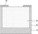
본 발명에 의한 1T 디램 소자는 기본적으로, 도 3과 같이, 전기적으로 고립되고 함몰된 반도체 바디(32)와; 상기 반도체 바디의 함몰된 부분에 형성된 게이트 절연막(52)과; 상기 게이트 절연막 상에 분리 절연막(54)을 사이에 두고 상기 반도체 바디의 함몰된 부분에 채워진 제 1 및 제 2 게이트(62)(64)를 포함하여 구성된 것을 특징으로 한다.The 1T DRAM device according to the present invention basically includes an electrically isolated and
여기서, 상기 제 1 및 제 2 게이트(62)(64)는 상기 반도체 바디(32)의 함몰된 부분에 수평으로 분리 절연막을 사이에 두며 형성될 수도 있으나, 도 3과 같이, 수직으로 적층되며 밑으로부터 제 2 게이트(62)->제 1 게이트(64) 순으로 채워지는 것이 바람직하다. 후자의 경우, 제 1 게이트(64) 양측에 위치한 반도체 바디(32) 상에 각각, 도 3과 같이, 상기 제 1 게이트(64)의 상부 일측과 일부 겹치며 소스(72) 및 드레인(74)이 형성된다. 도 3에서 도면부호 80은 제 1 게이트(64)와 드레인(74)이 겹쳐져(즉, overlap되어), 이들에 전압이 인가될 때 band bending으로 GIDL 현상이 일어나는 부분을 나타낸다.Here, the first and
따라서, 상기와 같은 구성을 함으로써, 상기 제 1 게이트(64)와 제 2 게이트(62)에 독립적으로 전압을 인가할 수 있게 되어 GIDL 현상을 이용한 쓰기 동작이 가능하여 종래 소자의 신뢰성 문제를 해결할 수 있음은 물론 데이터 "0"의 보유시간을 획기적으로 늘릴 수 있게 된다. 이에 관한 구체적 동작방법에 대해서는 후술한다.Therefore, the above configuration allows voltage to be independently applied to the
본 실시예의 보다 구체적인 구성으로, 도 3과 같이, 상기 반도체 바디(32)는 하측으로 매몰산화막(10), 측면으로 격리절연막(20) 또는 보이드(void, 미도시)로 이웃 소자와 전기적으로 고립될 수 있다.In a more specific configuration of the present embodiment, as shown in FIG. 3, the
그리고, 상기 반도체 바디(32)의 함몰된 부분은 상기 매몰산화막(10) 상에 반도체 바디(32)가 존재하도록 트렌치 형태(도 3 참조)로 형성될 수 있다.In addition, the recessed portion of the
더욱 구체적으로, 상기 반도체 바디(32)는 SOI 기판의 P형 실리콘층, 상기 소스(72) 및 드레인(74)은 N형 불순물 도핑층, 상기 제 1 게이트(64) 및 제 2 게이트(62)는 N형 불순물이 도핑된 실리콘계 물질(폴리 실리콘, 비정질 실리콘 등)로 각각 형성될 수 있다.
More specifically, the
[1T 디램 소자의 동작방법에 관한 실시예][Example of Operation Method of 1T DRAM Device]
다음, 상기 구조에 관한 실시예(SOI 기판의 P형 실리콘층을 반도체 바디로 하는 실시예)에 따른 1T 디램 소자의 동작방법에 관하여 설명한다.Next, an operation method of the 1T DRAM device according to the embodiment of the above structure (an embodiment in which the P-type silicon layer of the SOI substrate is the semiconductor body) will be described.
먼저, 쓰기 동작은 제 1 게이트(64) 및 제 2 게이트(62)에 각각 음의 전압을 인가하고, 소스(72)는 접지, 드레인(74)은 양의 전압을 인가하여, 제 1 게이트(64)와 드레인(74)이 겹쳐진 부분(80)에 band bending으로 GIDL 현상이 일어나도록 함으로써, 이때 발생한 홀(hole)이 플로팅되어 있는 반도체 바디(32)에 축적되도록 한다.First, in the write operation, a negative voltage is applied to the
여기서, 상기 제 1 게이트(64)에 인가된 음의 전압(negative voltage)이 상기 제 2 게이트에 인가된 음의 전압보다 절대값이 더 큰 것으로 함이 바람직한데, 이는 제 1 게이트(64)와 드레인(74)이 겹쳐진 부분(80)에 보다 큰 band bending으로 보다 많은 GIDL 전류가 발생되어 쓰기 속도를 높일 수 있기 때문이다.Here, it is preferable that the negative voltage applied to the
이에 대한 구체적인 일 예로, 도 4와 같이, 데이터 "1"을 쓰기 위하여(Write 1) 제 1 게이트(64, Gate 1)에 -3V, 제 2 게이트(62, Gate 2)에 -1V, 드레인(74, Drain)에 3V를 각각 인가할 수 있다.As an example of this, as shown in FIG. 4, in order to write data "1" (Write 1), -3V is applied to the first gate 64 (Gate 1), -1V is applied to the second gate 62 (Gate 2), and a drain ( 74V can be applied to each of the 3V.
다음, 지우기 동작은 P형 반도체 바디(32)에 양의 전압을 인가하고, N형 소스(72)/드레인(74) 및/또는 제 1, 2 게이트(64)(62)에는, 도 4와 같이, 모두 0V를 인가하여, 반도체 바디와 소스/드레인 사이에 순방향 바이어스가 가해지도록 함으로써, 반도체 바디(32)에 축적된 홀을 제거한다.Next, the erase operation applies a positive voltage to the P-
그리고, 읽기 동작은 일 예로, 도 4와 같이, 데이터 "1"을 읽기 위하여(Read 1) 또는 데이터 "0"을 읽기 위하여(Read 0) 모두 제 1 게이트(64, Gate 1)에 0V, 제 2 게이트(62, Gate 2)에 -0.5V, 소스(72)에 0V, 드레인(74, Drain)에 1.5V를 각각 인가하여 소스(72)와 드레인(74) 간에 흐르는 전류를 센싱함으로써, 반도체 바디(32)에 홀이 저장된 상태를 읽을 수 있다. 즉, 도 5와 같이, 반도체 바디(32)에 홀이 저장되어 있을 경우(Read 1의 경우)에는 동일한 바이어스 조건에서도 그렇지 않은 경우(Read 0의 경우)보다 문턱전압이 상대적으로 낮아져 높은 전류가 흐르게 되는데, 이를 센싱함으로써, 소자에 저장된 데이터를 읽게 된다.For example, as shown in FIG. 4, 0 V is applied to the first gate 64 (Gate 1) to read data “1” (Read 1) or read data “0” (Read 0). The semiconductor is sensed by sensing the current flowing between the
한편, 홀드(hold) 동작은, 상부 게이트인 제 1 게이트(64)를 접지시켜 드레인(74)과의 겹쳐진 부분(80)에서 GIDL 현상 발생되지 않도록 하고, 하부 게이트인 제 2 게이트(62)는 음의 전압을 인가하여 반도체 바디(32)에 축적된 홀을 잡아두는 방식으로 하게 된다.On the other hand, the hold operation is to ground the
이에 대한 구체적인 일 예로, 도 4와 같이, 데이터 "1"을 쓰기한 다음 읽기 전에 홀드(hold)하기 위하여, 소스(72)/드레인(74, Drain) 및 제 1 게이트(64, Gate 1)에 0V, 제 2 게이트(62, Gate 2)에 -1V를 각각 인가할 수 있다.As a specific example of this, as shown in FIG. 4, in order to hold the data “1” before writing and holding it, the
데이터 "0"을 쓰기한 다음(즉, 지우기 동작 후) 읽기 전에 홀드(hold)하기 위하여도 상기와 같은 동일한 바이어스 조건으로 동작할 수 있다(도 4 참조).The same bias condition as described above may also be used to hold the data " 0 " after writing (i.e., after the erase operation) and before reading (see FIG. 4).
상기와 같이, 동일한 바이어스 조건으로 데이터 "1" 및 데이터 "0" 쓰기한 다음 읽기 전에 각각 홀드 동작을 하였음에도, 데이터 "0"의 보유시간(retention time)은 도 6에 도시된 바와 같이, 데이터 "1"의 보유시간 만큼 획기적으로 증가됨을 알 수 있다.
As described above, even when the data " 1 " and the data " 0 " are written and held before the read, respectively, under the same bias condition, the retention time of the data " 0 " It can be seen that the increase significantly by the retention time of 1 ".
[1T 디램 소자의 제조방법에 관한 실시예][Example of Manufacturing Method of 1T DRAM Device]
한편, 상기 구조에 관한 실시예(SOI 기판의 P형 실리콘층을 반도체 바디로 하는 실시예)에 따른 1T 디램 소자의 제조방법에 관한 실시예를, 도 7 내지 도 13을 참조하며 설명하면 하기와 같다.Meanwhile, an embodiment of a method of manufacturing a 1T DRAM device according to an embodiment of the above structure (an embodiment in which a P-type silicon layer of a SOI substrate is a semiconductor body) will be described with reference to FIGS. 7 to 13. same.
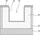
우선, SOI 기판에 액티브 영역을 정의하고, 도 7과 같이, 상기 액티브 영역 상에 식각 마스크(40)를 형성한다(제 1 단계). 이때, 상기 액티브 영역 정의시 소자를 격리하기 위한 격리절연막(20) 또는 보이드(void)가 SOI 기판의 매몰산화막(10) 상의 실리콘 액티브 영역(30)을 감싸게 된다. 또한, 상기 식각 마스크(40)는 실리콘과 식각 선택비가 큰 물질이면 어느 것으로 형성되어도 무방하나, 산화막으로 형성됨이 바람직하다.First, an active region is defined in an SOI substrate, and an
이어, 도 8과 같이, 상기 식각 마스크(40)로 상기 SOI 기판의 실리콘(32)을 식각하여 트렌치(34)를 형성하되, 상기 트렌치 바닥에 상기 실리콘이 남아 있도록 한다(제 2 단계).Subsequently, as shown in FIG. 8, the
다음, 도 9와 같이, 상기 트렌치(34) 상에 게이트 절연막(52)을 형성한다(제 3 단계). 이때, 상기 게이트 절연막(52)을 형성은 통상의 열 산화공정에 의함이 바람직하다.Next, as shown in FIG. 9, a
이후, 도 10 내지 도 12와 같이, 상기 게이트 절연막(52) 상에 제 2 게이트(62)->분리 절연막(54)->제 1 게이트(64) 순으로 적층 형성하며 상기 트렌치(34)를 채운다(제 4 단계). 여기서, 상기 제 1 게이트(64) 및 상기 제 2 게이트(62)는 불순물이 도핑된 실리콘계 물질(폴리 실리콘, 비정질 실리콘 등)로 형성되고, 상기 분리 절연막 형성 또한 통상의 열 산화공정에 의함이 바람직하다. 이는, 도 10과 같이, 상기 제 2 게이트(62) 형성시 이전에 형성된 게이트 절연막(52)이 일부 식각되더라도, 도 11과 같이, 분리 절연막 형성시 상기 식각된 게이트 절연막을 다시 형성할 수 있기 때문이다(도면부호 52b 참조).10 to 12, the
마지막으로, 도 13과 같이, 상기 제 4 단계 이후에 상기 식각 마스크(40)를 제거하고 이온주입 공정으로 소스(72) 및 드레인(74)을 형성한다(제 5 단계). 그러나, 상기 소스(72) 및 드레인(74) 형성을 위한 이온주입 공정은 상기 제 1 단계의 액티브 영역을 정의하기 직전 또는 직후에 이루어 질 수도 있다.Finally, as shown in FIG. 13, after the fourth step, the
기타, 미설명된 공정단계는 통상의 1T 디램 소자의 제조방법에 따를 수 있으므로, 이에 대한 설명은 생략한다.In addition, since the process steps that are not described may be in accordance with a conventional method for manufacturing a 1T DRAM device, description thereof will be omitted.
10: 매몰산화막
20: 격리절연막
30: 액티브 영역
32: 실리콘 바디(반도체 바디)
34: 트렌치
40: 식각 마스크
52, 52a, 52b: 게이트 절연막
54: 분리 절연막
62: 제 2 게이트
64: 제 1 게이트
72: 소스
74: 드레인
80: GIDL 현상이 일어나는 부분10: investment oxide
20: insulating film
30: active area
32: silicone body (semiconductor body)
34: trench
40: etching mask
52, 52a, 52b: gate insulating film
54: separation insulating film
62: second gate
64: first gate
72: source
74: drain
80: where GIDL occurs
Claims (10)
Translated fromKorean상기 반도체 바디의 함몰된 부분에 형성된 게이트 절연막과;
상기 게이트 절연막 상에 분리 절연막을 사이에 두고 상기 반도체 바디의 함몰된 부분에 채워진 제 1 및 제 2 게이트를 포함하여 구성된 것을 특징으로 하는 함몰된 바디에 두개의 게이트를 갖는 1T 디램 소자.
An electrically isolated and recessed semiconductor body;
A gate insulating film formed on the recessed portion of the semiconductor body;
And a first gate and a second gate filled in the recessed portion of the semiconductor body with a separation insulating layer interposed therebetween on the gate insulating layer. 1T DRAM device having two gates in the recessed body.
상기 제 1 및 제 2 게이트는 상기 반도체 바디의 함몰된 부분에 수직하게 적층되며 밑으로부터 제 2 게이트->제 1 게이트 순으로 채워지고,
상기 제 1 게이트 양측의 상기 반도체 바디 상에 상기 제 1 게이트의 상부 일측과 일부 겹치며 소스 및 드레인이 형성된 것을 특징으로 하는 함몰된 바디에 두개의 게이트를 갖는 1T 디램 소자.
The method of claim 1,
The first and second gates are stacked perpendicular to the recessed portion of the semiconductor body and are filled in the order from the second gate to the first gate from below,
The 1T DRAM device having two gates in the recessed body, wherein a source and a drain are partially overlapped with one upper portion of the first gate on the semiconductor body at both sides of the first gate.
상기 반도체 바디는 하측으로 매몰산화막, 측면으로 격리절연막 또는 보이드(void)로 이웃 소자와 전기적으로 고립된 것을 특징으로 하는 함몰된 바디에 두개의 게이트를 갖는 1T 디램 소자.
The method according to claim 1 or 2,
And the semiconductor body has two gates in the recessed body, wherein the semiconductor body is electrically isolated from the neighboring device with a buried oxide film on the lower side, and an insulating insulating film or a void on the side.
상기 반도체 바디의 함몰된 부분은 상기 매몰산화막 상에 반도체 바디가 존재하도록 트렌치 형태로 형성된 것을 특징으로 하는 함몰된 바디에 두개의 게이트를 갖는 1T 디램 소자.
The method of claim 3, wherein
The recessed portion of the semiconductor body is formed in a trench form so that the semiconductor body on the buried oxide film 1T DRAM device having two gates in the recessed body.
상기 제 1 게이트 및 상기 제 2 게이트는 각각 음의 전압을 인가하고,
상기 소스는 접지, 상기 드레인은 양의 전압을 인가하여 쓰기 동작을 하는 것을 특징으로 하는 함몰된 바디에 두개의 게이트를 갖는 1T 디램 소자의 동작방법.
In the method of operating the 1T DRAM device according to claim 2,
The first gate and the second gate apply a negative voltage, respectively,
The method of claim 1, wherein the source is grounded, and the drain is applied with a positive voltage to perform a write operation.
상기 제 1 게이트에 인가된 음의 전압이 상기 제 2 게이트에 인가된 음의 전압보다 절대값이 더 큰 것을 특징으로 하는 함몰된 바디에 두개의 게이트를 갖는 1T 디램 소자의 동작방법.
The method of claim 5, wherein
The method of operating a 1T DRAM device having two gates in the recessed body, characterized in that the negative voltage applied to the first gate is greater than the negative voltage applied to the second gate.
상기 제 1 게이트는 접지시키고,
상기 제 2 게이트는 음의 전압을 인가하여 홀드(hold) 동작을 하는 것을 특징으로 하는 함몰된 바디에 두개의 게이트를 갖는 1T 디램 소자의 동작방법.
The method according to claim 5 or 6,
The first gate is grounded,
The second gate is a method of operating a 1T DRAM device having two gates in the recessed body, characterized in that the holding (hold) by applying a negative voltage.
SOI 기판에 액티브 영역을 정의하고, 상기 액티브 영역 상에 식각 마스크를 형성하는 제 1 단계와;
상기 식각 마스크로 상기 SOI 기판의 실리콘을 식각하여 트렌치를 형성하되, 상기 트렌치 바닥에 상기 실리콘이 남아 있도록 하는 제 2 단계와;
상기 트렌치 상에 게이트 절연막을 형성하는 제 3 단계와;
상기 게이트 절연막 상에 제 2 게이트->분리 절연막->제 1 게이트 순으로 적층 형성하며 상기 트렌치를 채우는 제 4 단계를 포함하여 구성된 것을 특징으로 하는 함몰된 바디에 두개의 게이트를 갖는 1T 디램 소자의 제조방법.
In the method of manufacturing a 1T DRAM device according to claim 4,
Defining an active region in the SOI substrate and forming an etch mask on the active region;
Forming a trench by etching silicon of the SOI substrate with the etching mask, wherein the silicon remains at the bottom of the trench;
Forming a gate insulating film on the trench;
Forming a second gate-> separating insulating film-> first gate on the gate insulating film, and filling the trench with a fourth step, wherein the 1T DRAM device having two gates is formed in the recessed body. Manufacturing method.
상기 제 4 단계 이후에 상기 식각 마스크를 제거하고 이온주입 공정으로 소스 및 드레인을 형성하는 제 5 단계를 더 포함하는 것을 특징으로 하는 함몰된 바디에 두개의 게이트를 갖는 1T 디램 소자의 제조방법.
The method of claim 8,
And a fifth step of removing the etch mask after the fourth step and forming a source and a drain by an ion implantation process.
상기 제 1 게이트 및 상기 제 2 게이트는 불순물이 도핑된 실리콘계 물질로 형성되고,
상기 게이트 절연막 및 상기 분리 절연막 형성은 열 산화공정에 의하고,
상기 분리 절연막을 형성할 때 상기 제 2 게이트 형성시 일부 식각된 상기 게이트 절연막도 다시 형성되는 것을 특징으로 하는 함몰된 바디에 두개의 게이트를 갖는 1T 디램 소자의 제조방법.The method according to claim 8 or 9,
The first gate and the second gate are formed of a silicon-based material doped with impurities,
Forming the gate insulating film and the isolation insulating film by a thermal oxidation process,
And forming the gate insulating film partially etched when the second gate is formed when the isolation insulating film is formed.
Priority Applications (1)
| Application Number | Priority Date | Filing Date | Title |
|---|---|---|---|
| KR1020100056615AKR101163711B1 (en) | 2010-06-15 | 2010-06-15 | 1t dram device having two gates on recessed body and method of operating and fabricating the same |
Applications Claiming Priority (1)
| Application Number | Priority Date | Filing Date | Title |
|---|---|---|---|
| KR1020100056615AKR101163711B1 (en) | 2010-06-15 | 2010-06-15 | 1t dram device having two gates on recessed body and method of operating and fabricating the same |
Publications (2)
| Publication Number | Publication Date |
|---|---|
| KR20110136532Atrue KR20110136532A (en) | 2011-12-21 |
| KR101163711B1 KR101163711B1 (en) | 2012-07-09 |
Family
ID=45503169
Family Applications (1)
| Application Number | Title | Priority Date | Filing Date |
|---|---|---|---|
| KR1020100056615AActiveKR101163711B1 (en) | 2010-06-15 | 2010-06-15 | 1t dram device having two gates on recessed body and method of operating and fabricating the same |
Country Status (1)
| Country | Link |
|---|---|
| KR (1) | KR101163711B1 (en) |
Cited By (17)
| Publication number | Priority date | Publication date | Assignee | Title |
|---|---|---|---|---|
| WO2018101770A1 (en)* | 2016-12-01 | 2018-06-07 | 한양대학교 산학협력단 | Two-terminal vertical type 1t-dram and manufacturing method therefor |
| WO2019055415A1 (en)* | 2017-09-12 | 2019-03-21 | Applied Materials, Inc. | Apparatus and methods for manufacturing semiconductor structures using protective barrier layer |
| US10714331B2 (en) | 2018-04-04 | 2020-07-14 | Applied Materials, Inc. | Method to fabricate thermally stable low K-FinFET spacer |
| US10748783B2 (en) | 2018-07-25 | 2020-08-18 | Applied Materials, Inc. | Gas delivery module |
| US10854483B2 (en) | 2017-11-16 | 2020-12-01 | Applied Materials, Inc. | High pressure steam anneal processing apparatus |
| US10957533B2 (en) | 2018-10-30 | 2021-03-23 | Applied Materials, Inc. | Methods for etching a structure for semiconductor applications |
| US10998200B2 (en) | 2018-03-09 | 2021-05-04 | Applied Materials, Inc. | High pressure annealing process for metal containing materials |
| US11018032B2 (en) | 2017-08-18 | 2021-05-25 | Applied Materials, Inc. | High pressure and high temperature anneal chamber |
| US11227797B2 (en) | 2018-11-16 | 2022-01-18 | Applied Materials, Inc. | Film deposition using enhanced diffusion process |
| US11462417B2 (en) | 2017-08-18 | 2022-10-04 | Applied Materials, Inc. | High pressure and high temperature anneal chamber |
| US11527421B2 (en) | 2017-11-11 | 2022-12-13 | Micromaterials, LLC | Gas delivery system for high pressure processing chamber |
| US11581183B2 (en) | 2018-05-08 | 2023-02-14 | Applied Materials, Inc. | Methods of forming amorphous carbon hard mask layers and hard mask layers formed therefrom |
| US11610773B2 (en) | 2017-11-17 | 2023-03-21 | Applied Materials, Inc. | Condenser system for high pressure processing system |
| US11705337B2 (en) | 2017-05-25 | 2023-07-18 | Applied Materials, Inc. | Tungsten defluorination by high pressure treatment |
| US11749555B2 (en) | 2018-12-07 | 2023-09-05 | Applied Materials, Inc. | Semiconductor processing system |
| US11901222B2 (en) | 2020-02-17 | 2024-02-13 | Applied Materials, Inc. | Multi-step process for flowable gap-fill film |
| US12198951B2 (en) | 2017-03-10 | 2025-01-14 | Applied Materials, Inc. | High pressure wafer processing systems and related methods |
Family Cites Families (2)
| Publication number | Priority date | Publication date | Assignee | Title |
|---|---|---|---|---|
| US7531404B2 (en) | 2005-08-30 | 2009-05-12 | Intel Corporation | Semiconductor device having a metal gate electrode formed on an annealed high-k gate dielectric layer |
| KR100880377B1 (en) | 2007-08-03 | 2009-01-28 | 한국과학기술원 | Vertical nanoshell field effect transistor and fused memory device, and manufacturing method thereof |
- 2010
- 2010-06-15KRKR1020100056615Apatent/KR101163711B1/enactiveActive
Cited By (24)
| Publication number | Priority date | Publication date | Assignee | Title |
|---|---|---|---|---|
| US10886274B2 (en) | 2016-12-01 | 2021-01-05 | Industry-University Cooperation Foundation Hanyang University | Two-terminal vertical 1T-DRAM and method of fabricating the same |
| WO2018101770A1 (en)* | 2016-12-01 | 2018-06-07 | 한양대학교 산학협력단 | Two-terminal vertical type 1t-dram and manufacturing method therefor |
| US12198951B2 (en) | 2017-03-10 | 2025-01-14 | Applied Materials, Inc. | High pressure wafer processing systems and related methods |
| US11705337B2 (en) | 2017-05-25 | 2023-07-18 | Applied Materials, Inc. | Tungsten defluorination by high pressure treatment |
| US11462417B2 (en) | 2017-08-18 | 2022-10-04 | Applied Materials, Inc. | High pressure and high temperature anneal chamber |
| US11694912B2 (en) | 2017-08-18 | 2023-07-04 | Applied Materials, Inc. | High pressure and high temperature anneal chamber |
| US11469113B2 (en) | 2017-08-18 | 2022-10-11 | Applied Materials, Inc. | High pressure and high temperature anneal chamber |
| US11018032B2 (en) | 2017-08-18 | 2021-05-25 | Applied Materials, Inc. | High pressure and high temperature anneal chamber |
| US11177128B2 (en) | 2017-09-12 | 2021-11-16 | Applied Materials, Inc. | Apparatus and methods for manufacturing semiconductor structures using protective barrier layer |
| WO2019055415A1 (en)* | 2017-09-12 | 2019-03-21 | Applied Materials, Inc. | Apparatus and methods for manufacturing semiconductor structures using protective barrier layer |
| US11527421B2 (en) | 2017-11-11 | 2022-12-13 | Micromaterials, LLC | Gas delivery system for high pressure processing chamber |
| US11756803B2 (en) | 2017-11-11 | 2023-09-12 | Applied Materials, Inc. | Gas delivery system for high pressure processing chamber |
| US10854483B2 (en) | 2017-11-16 | 2020-12-01 | Applied Materials, Inc. | High pressure steam anneal processing apparatus |
| US11610773B2 (en) | 2017-11-17 | 2023-03-21 | Applied Materials, Inc. | Condenser system for high pressure processing system |
| US10998200B2 (en) | 2018-03-09 | 2021-05-04 | Applied Materials, Inc. | High pressure annealing process for metal containing materials |
| US11881411B2 (en) | 2018-03-09 | 2024-01-23 | Applied Materials, Inc. | High pressure annealing process for metal containing materials |
| US10714331B2 (en) | 2018-04-04 | 2020-07-14 | Applied Materials, Inc. | Method to fabricate thermally stable low K-FinFET spacer |
| US11581183B2 (en) | 2018-05-08 | 2023-02-14 | Applied Materials, Inc. | Methods of forming amorphous carbon hard mask layers and hard mask layers formed therefrom |
| US10748783B2 (en) | 2018-07-25 | 2020-08-18 | Applied Materials, Inc. | Gas delivery module |
| US11361978B2 (en) | 2018-07-25 | 2022-06-14 | Applied Materials, Inc. | Gas delivery module |
| US10957533B2 (en) | 2018-10-30 | 2021-03-23 | Applied Materials, Inc. | Methods for etching a structure for semiconductor applications |
| US11227797B2 (en) | 2018-11-16 | 2022-01-18 | Applied Materials, Inc. | Film deposition using enhanced diffusion process |
| US11749555B2 (en) | 2018-12-07 | 2023-09-05 | Applied Materials, Inc. | Semiconductor processing system |
| US11901222B2 (en) | 2020-02-17 | 2024-02-13 | Applied Materials, Inc. | Multi-step process for flowable gap-fill film |
Also Published As
| Publication number | Publication date |
|---|---|
| KR101163711B1 (en) | 2012-07-09 |
Similar Documents
| Publication | Publication Date | Title |
|---|---|---|
| KR101163711B1 (en) | 1t dram device having two gates on recessed body and method of operating and fabricating the same | |
| TW544911B (en) | Semiconductor device | |
| TWI427776B (en) | Method, device and system for a memory unit having a floating body | |
| JP3898715B2 (en) | Semiconductor device and manufacturing method thereof | |
| TWI517307B (en) | Vertical type capacitorless DRAM memory cell, DRAM array and operation method thereof | |
| US7851859B2 (en) | Single transistor memory device having source and drain insulating regions and method of fabricating the same | |
| US8084316B2 (en) | Method of fabricating single transistor floating-body DRAM devices having vertical channel transistor structures | |
| KR100945511B1 (en) | Semiconductor device and manufacturing method thereof | |
| US20100085813A1 (en) | Method of driving a semiconductor memory device and a semiconductor memory device | |
| US7361545B2 (en) | Field effect transistor with buried gate pattern | |
| KR101337763B1 (en) | Methods, devices, and systems relating to memory cells having a floating body | |
| JPH08316337A (en) | Semiconductor memory device | |
| JP2008177273A (en) | Semiconductor memory device and manufacturing method of semiconductor memory device | |
| US20120224438A1 (en) | Semiconductor memory device | |
| KR101130018B1 (en) | Semiconductor Device and Method for Manufacturing the same | |
| JP6439705B2 (en) | Semiconductor device and memory circuit | |
| CN102088028A (en) | Flash memory cell on SeOI having second control gate buried under insulating layer | |
| US7132751B2 (en) | Memory cell using silicon carbide | |
| JP2008153567A (en) | Semiconductor memory and manufacturing method thereof | |
| TW200816397A (en) | Flash memory device with single-poly structure and method for manufacturing the same | |
| US20110134690A1 (en) | METHOD OF CONTROLLING A DRAM MEMORY CELL ON THE SeOI HAVING A SECOND CONTROL GATE BURIED UNDER THE INSULATING LAYER | |
| US20080237689A1 (en) | Nonvolatile semiconductor memory device, method for manufacturing the same, and semiconductor device | |
| CN108257970A (en) | Semiconductor devices and its manufacturing method | |
| JP2008098467A (en) | Semiconductor memory device and manufacturing method thereof | |
| KR100583729B1 (en) | Flash memory cell having a dual gate insulating film and method of forming the same |
Legal Events
| Date | Code | Title | Description |
|---|---|---|---|
| A201 | Request for examination | ||
| PA0109 | Patent application | Patent event code:PA01091R01D Comment text:Patent Application Patent event date:20100615 | |
| PA0201 | Request for examination | ||
| E902 | Notification of reason for refusal | ||
| PE0902 | Notice of grounds for rejection | Comment text:Notification of reason for refusal Patent event date:20110818 Patent event code:PE09021S01D | |
| PG1501 | Laying open of application | ||
| E701 | Decision to grant or registration of patent right | ||
| PE0701 | Decision of registration | Patent event code:PE07011S01D Comment text:Decision to Grant Registration Patent event date:20120330 | |
| GRNT | Written decision to grant | ||
| PR0701 | Registration of establishment | Comment text:Registration of Establishment Patent event date:20120702 Patent event code:PR07011E01D | |
| PR1002 | Payment of registration fee | Payment date:20120702 End annual number:3 Start annual number:1 | |
| PG1601 | Publication of registration | ||
| FPAY | Annual fee payment | Payment date:20150629 Year of fee payment:4 | |
| PR1001 | Payment of annual fee | Payment date:20150629 Start annual number:4 End annual number:4 | |
| FPAY | Annual fee payment | Payment date:20160204 Year of fee payment:5 | |
| PR1001 | Payment of annual fee | Payment date:20160204 Start annual number:5 End annual number:5 | |
| FPAY | Annual fee payment | Payment date:20170626 Year of fee payment:6 | |
| PR1001 | Payment of annual fee | Payment date:20170626 Start annual number:6 End annual number:6 | |
| FPAY | Annual fee payment | Payment date:20180620 Year of fee payment:7 | |
| PR1001 | Payment of annual fee | Payment date:20180620 Start annual number:7 End annual number:7 | |
| FPAY | Annual fee payment | Payment date:20190902 Year of fee payment:8 | |
| PR1001 | Payment of annual fee | Payment date:20190902 Start annual number:8 End annual number:8 | |
| PR1001 | Payment of annual fee | Payment date:20200715 Start annual number:9 End annual number:9 | |
| PR1001 | Payment of annual fee | Payment date:20211026 Start annual number:10 End annual number:10 | |
| PR1001 | Payment of annual fee | Payment date:20220706 Start annual number:11 End annual number:11 | |
| PR1001 | Payment of annual fee | Payment date:20230620 Start annual number:12 End annual number:12 | |
| PR1001 | Payment of annual fee | Payment date:20240625 Start annual number:13 End annual number:13 | |
| PR1001 | Payment of annual fee | Payment date:20250624 Start annual number:14 End annual number:14 |